Embed Size (px)
Citation preview
© Semiconductor Components Industries, LLC, 2017
July, 2018 − Rev. 51 Publication Order Number:
NCP110/D
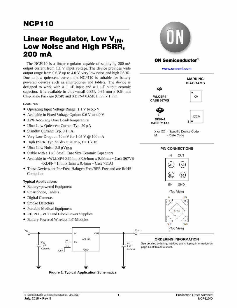
NCP110
Linear Regulator, Low VIN,Low Noise and High PSRR,200 mA
The NCP110 is a linear regulator capable of supplying 200 mAoutput current from 1.1 V input voltage. The device provides wideoutput range from 0.6 V up to 4.0 V, very low noise and high PSRR.Due to low quiescent current the NCP110 is suitable for batterypowered devices such as smartphones and tablets. The device isdesigned to work with a 1 �F input and a 1 �F output ceramiccapacitor. It is available in ultra−small 0.35P, 0.64 mm x 0.64 mmChip Scale Package (CSP) and XDFN4 0.65P, 1 mm x 1 mm.
Features• Operating Input Voltage Range: 1.1 V to 5.5 V
• Available in Fixed Voltage Option: 0.6 V to 4.0 V
• ±2% Accuracy Over Load/Temperature
• Ultra Low Quiescent Current Typ. 20 �A
• Standby Current: Typ. 0.1 �A
• Very Low Dropout: 70 mV for 1.05 V @ 100 mA
• High PSRR: Typ. 95 dB at 20 mA, f = 1 kHz
• Ultra Low Noise: 8.8 �VRMS
• Stable with a 1 �F Small Case Size Ceramic Capacitors
• Available in −WLCSP4 0.64mm x 0.64mm x 0.33mm − Case 567VS−XDFN4 1mm x 1mm x 0.4mm − Case 711AJ
• These Devices are Pb−Free, Halogen Free/BFR Free and are RoHSCompliant
Typical Applications• Battery−powered Equipment
• Smartphone, Tablets
• Digital Cameras
• Smoke Detectors
• Portable Medical Equipment
• RF, PLL, VCO and Clock Power Supplies
• Battery Powered Wireless IoT Modules
IN
EN
GND
OUT
OFF
ON
Figure 1. Typical Application Schematics
VOUT
COUT1 �FCeramic
VIN
NCP110CIN1 �FCeramic
MARKINGDIAGRAMS
www.onsemi.com
X or XX = Specific Device CodeM = Date Code
See detailed ordering, marking and shipping information onpage 14 of this data sheet.
ORDERING INFORMATION
PIN CONNECTIONS
XDFN4CASE 711AJ
A1 A2
B1 B2
IN OUT
EN GND
(Top View)
(Top View)
WLCSP4CASE 567VS
1 XX M
1
XM
NCP110
www.onsemi.com2
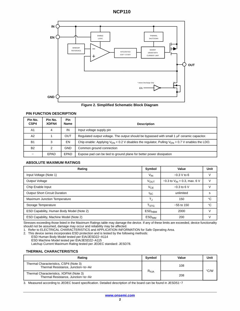
Figure 2. Simplified Schematic Block Diagram
IN
THERMAL
SHUTDOWN
MOSFET
DRIVER WITH
CURRENT LIMIT
INTEGRATED
SOFT−START
BANDGAP
REFERENCE
ENABLE
LOGICEN
OUT
GND
EN
* Active Discharge Only
PIN FUNCTION DESCRIPTION
Pin No.CSP4
Pin No.XDFN4
PinName Description
A1 4 IN Input voltage supply pin
A2 1 OUT Regulated output voltage. The output should be bypassed with small 1 �F ceramic capacitor.
B1 3 EN Chip enable: Applying VEN < 0.2 V disables the regulator, Pulling VEN > 0.7 V enables the LDO.
B2 2 GND Common ground connection
− EPAD EPAD Expose pad can be tied to ground plane for better power dissipation
ABSOLUTE MAXIMUM RATINGS
Rating Symbol Value Unit
Input Voltage (Note 1) VIN −0.3 V to 6 V
Output Voltage VOUT −0.3 to VIN + 0.3, max. 6 V V
Chip Enable Input VCE −0.3 to 6 V V
Output Short Circuit Duration tSC unlimited s
Maximum Junction Temperature TJ 150 °C
Storage Temperature TSTG −55 to 150 °C
ESD Capability, Human Body Model (Note 2) ESDHBM 2000 V
ESD Capability, Machine Model (Note 2) ESDMM 200 V
Stresses exceeding those listed in the Maximum Ratings table may damage the device. If any of these limits are exceeded, device functionalityshould not be assumed, damage may occur and reliability may be affected.1. Refer to ELECTRICAL CHARACTERISTICS and APPLICATION INFORMATION for Safe Operating Area.2. This device series incorporates ESD protection and is tested by the following methods:
ESD Human Body Model tested per EIA/JESD22−A114ESD Machine Model tested per EIA/JESD22−A115Latchup Current Maximum Rating tested per JEDEC standard: JESD78.
THERMAL CHARACTERISTICS
Rating Symbol Value Unit
Thermal Characteristics, CSP4 (Note 3)Thermal Resistance, Junction−to−Air
R�JA
108
°C/WThermal Characteristics, XDFN4 (Note 3)
Thermal Resistance, Junction−to−Air 208
3. Measured according to JEDEC board specification. Detailed description of the board can be found in JESD51−7

NCP110
www.onsemi.com3
ELECTRICAL CHARACTERISTICS −40°C ≤ TJ ≤ 125°C; VIN = VOUT(NOM) + 0.3 V or 1.1 V, whichever is greater; IOUT = 1 mA, CIN =COUT = 1 �F, unless otherwise noted. VEN = 1.0 V. Typical values are at TJ = +25°C (Note 4).
Parameter Test Conditions Symbol Min Typ Max Unit
Operating Input Voltage VIN 1.1 5.5 V
Output Voltage Accuracy VIN = VOUT(NOM) + 0.3 V(VIN ≥ 1.1 V)
VOUT(NOM) ≤ 1.5 V VOUT −30 +30 mV
VOUT(NOM) > 1.5 V −2 +2 %
Line Regulation VOUT(NOM) + 0.5 V ≤ VIN ≤ 5.5 V, (VIN ≥ 1.1 V) LineReg 0.02 %/V
Load Regulation IOUT = 1 mA to 200 mA LoadReg 0.001 %/mA
Dropout Voltage (Note 5) VOUT(NOM) = 1.05 V IOUT = 50 mA VDO 40 70 mV
IOUT = 100 mA 70 130
VOUT(NOM) = 1.20 V IOUT = 110 mA 60 140
IOUT = 200 mA 110 190
VOUT(NOM) = 1.80 V IOUT = 200 mA 65 120
VOUT(NOM) = 2.80 V IOUT = 200 mA 45 100
Output Current Limit VOUT = 90% VOUT(NOM) ICL 225 300mA
Short Circuit Current VOUT = 0 V ISC 300
Quiescent Current IOUT = 0 mA IQ 20 25 �A
Shutdown Current VEN ≤ 0.2 V, VIN = 1.1 V IDIS 0.01 1.0 �A
EN Pin Threshold Voltage EN Input Voltage “H” VENH 0.7V
EN Input Voltage “L” VENL 0.2
EN Pull Down Current VEN = 1.1 V IEN 0.2 0.5 �A
Turn−On Time COUT = 1 �F, From assertion of VEN to VOUT = 95% VOUT(NOM)
tON 120 �s
Power Supply Rejection Ratio IOUT = 20 mA,VIN = VOUT + 0.3 V
f = 100 Hzf = 1 kHzf = 10 kHzf = 100 kHz
PSRR 90958555
dB
Output Voltage Noise f = 10 Hz to 100 kHz VN 8.8 �VRMS
Thermal Shutdown Threshold Temperature rising TSDH 160 °C
Temperature falling TSDL 140 °C
Active Output Discharge Resis-tance
VEN < 0.2 V, Version A only RDIS 280 �
Product parametric performance is indicated in the Electrical Characteristics for the listed test conditions, unless otherwise noted. Productperformance may not be indicated by the Electrical Characteristics if operated under different conditions.4. Performance guaranteed over the indicated operating temperature range by design and/or characterization. Production tested at TA = 25°C.
Low duty cycle pulse techniques are used during the testing to maintain the junction temperature as close to ambient as possible.5. Dropout voltage is characterized when VOUT falls 0.02 x VOUT(NOM) below VOUT(NOM).6. Guaranteed by design.

NCP110
www.onsemi.com4
TYPICAL CHARACTERISTICS
1.06
1.055
1.05
1.045
1.04
1.035
1.03
VO
UT,
OU
TP
UT
VO
LTA
GE
(V
)
TJ, TEMPERATURE (°C)−40 1400 20 40 60 120100
Figure 3. Output Voltage vs. Temperature −VOUT,nom = 1.05 V − CSP4
IOUT = 1 mA
IOUT = 200 mA
1.205
VO
UT,
OU
TP
UT
VO
LTA
GE
(V
)
TJ, TEMPERATURE (°C)
Figure 4. Output Voltage vs. Temperature −VOUT,nom = 1.2 V − CSP4
IOUT = 1 mA
IOUT = 200 mA
1.2
1.195
1.19
1.185
1.8−20 80 −40 1400 20 40 60 120100−20 80
1.81
VO
UT,
OU
TP
UT
VO
LTA
GE
(V
)
TJ, TEMPERATURE (°C)
Figure 5. Output Voltage vs. Temperature −VOUT,nom = 1.8 V − CSP4
IOUT = 1 mA
IOUT = 200 mA
1.805
1.8
1.795
1.79
1.785
1.78
1LO
AD
RE
G, L
OA
D R
EG
ULA
TIO
N (
mV
)
TJ, TEMPERATURE (°C)
Figure 6. Load Regulation vs. Temperature
0.9
0.8
0.7
0.6
0.5
0.4
0.3
0.2
0.1
0
VIN = VOUT,NOM + 0.3 VIOUT = 1 mA to 200 mA
−40 1400 20 40 60 120100−20 80 −40 1400 20 40 60 120100−20 80
0
0.05
0.1
0.15
0.2
0.25
0.3
−40 −20 0 20 40 60 80 100 120 140
LIN
ER
EG
, LIN
E R
EG
ULA
TIO
N (
mV
/V)
TJ, TEMPERATURE (°C)
Figure 7. Line Regulation vs. Temperature
1000
I GN
D, G
RO
UN
D C
UR
RE
NT
(�A
)
IOUT, OUTPUT CURRENT (A)1u
Figure 8. Ground Current vs. Output Current −VOUT,nom = 1.2 V
10u 100u 1m 10m 100m 1
100
10
TJ = 25°C
TJ =−40°C
TJ = 125°C
NCP110
www.onsemi.com5
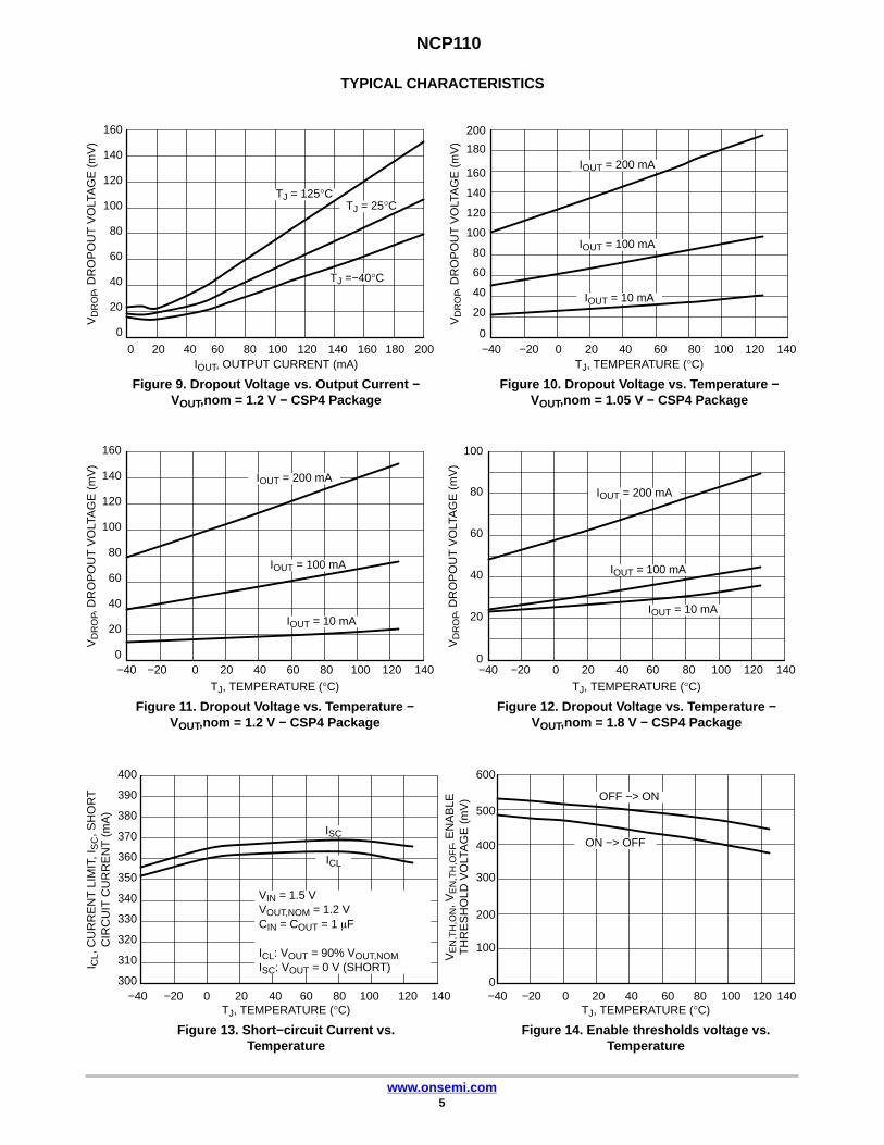
TYPICAL CHARACTERISTICS
160
VD
RO
P, D
RO
PO
UT
VO
LTA
GE
(m
V)
IOUT, OUTPUT CURRENT (mA)0
Figure 9. Dropout Voltage vs. Output Current −VOUT,nom = 1.2 V − CSP4 Package
40 80 180120 160 200
140
120
100
80
60
40
20
0
20 60 100 140
TJ = 25°C
TJ =−40°C
TJ = 125°C
160
VD
RO
P, D
RO
PO
UT
VO
LTA
GE
(m
V)
TJ, TEMPERATURE (°C)0
Figure 10. Dropout Voltage vs. Temperature −VOUT,nom = 1.05 V − CSP4 Package
40 80 120
140
120
100
80
60
40
20
020 60 100 140−20−40
180
200
IOUT = 200 mA
IOUT = 10 mA
IOUT = 100 mA
160
VD
RO
P, D
RO
PO
UT
VO
LTA
GE
(m
V)
TJ, TEMPERATURE (°C)
Figure 11. Dropout Voltage vs. Temperature −VOUT,nom = 1.2 V − CSP4 Package
140
120
100
80
60
40
20
0
IOUT = 200 mA
IOUT = 10 mA
IOUT = 100 mA
0 40 80 12020 60 100 140−20−40
VD
RO
P, D
RO
PO
UT
VO
LTA
GE
(m
V)
TJ, TEMPERATURE (°C)
Figure 12. Dropout Voltage vs. Temperature −VOUT,nom = 1.8 V − CSP4 Package
100
80
60
40
20
00 40 80 12020 60 100 140−20−40
IOUT = 200 mA
IOUT = 10 mA
IOUT = 100 mA
I CL,
CU
RR
EN
T L
IMIT
, IS
C, S
HO
RT
CIR
CU
IT C
UR
RE
NT
(m
A)
TJ, TEMPERATURE (°C)
Figure 13. Short−circuit Current vs.Temperature
400
0 40 80 12020 60 100 140−20−40
390
380
370
360
350
340
330
320
310
300
ICL
ISC
VIN = 1.5 VVOUT,NOM = 1.2 VCIN = COUT = 1 �F
ICL: VOUT = 90% VOUT,NOMISC: VOUT = 0 V (SHORT)
VE
N,T
H,O
N, V
EN
,TH
,OF
F, E
NA
BLE
TH
RE
SH
OLD
VO
LTA
GE
(m
V)
TJ, TEMPERATURE (°C)
Figure 14. Enable thresholds voltage vs.Temperature
600
0 40 80 12020 60 100 140−20−40
OFF −> ON
ON −> OFF
500
400
300
200
100
0

NCP110
www.onsemi.com6
I EN
, EN
AB
LE P
IN C
UR
RE
NT
(�A
)
TJ, TEMPERATURE (°C)
Figure 15. Enable Pin Current vs. Temperature
0.3
0 40 80 12020 60 100 140−20−40
0.25
0.2
0.15
0.1
0.05
0VEN = 1 V
I DIS
, DIS
AB
LE C
UR
RE
NT
(nA
)
TJ, TEMPERATURE (°C)
Figure 16. Disable Current vs. Temperature
160
0 40 80 12020 60 100 140−20−40
VEN = 0 V
140
120
100
80
60
40
20
0
RD
IS, D
ISC
HA
RG
E R
ES
IST
IVIT
Y (�
)
TJ, TEMPERATURE (°C)
Figure 17. Discharge Resistivity vs.Temperature
300
0 40 80 12020 60 100 140−20−40
290
280
270
260
250
240
230
220
210
200
VIN = 1.5 VVOUT,nom = 1.2 V
ES
R, E
QU
IVA
LEN
T S
ER
IES
RE
SIS
TAN
CE
(�
)
IOUT, OUTPUT CURRENT (mA)
Figure 18. Maximum COUT ESR Value vs.Output Current
100
0 40 80 12020 60 100 140
VOUT,nom = 1.2 VCOUT = 1 �F
Unstable Region
Stable Region
10
1
0.1
0.01160 180 200
NCP110
www.onsemi.com7
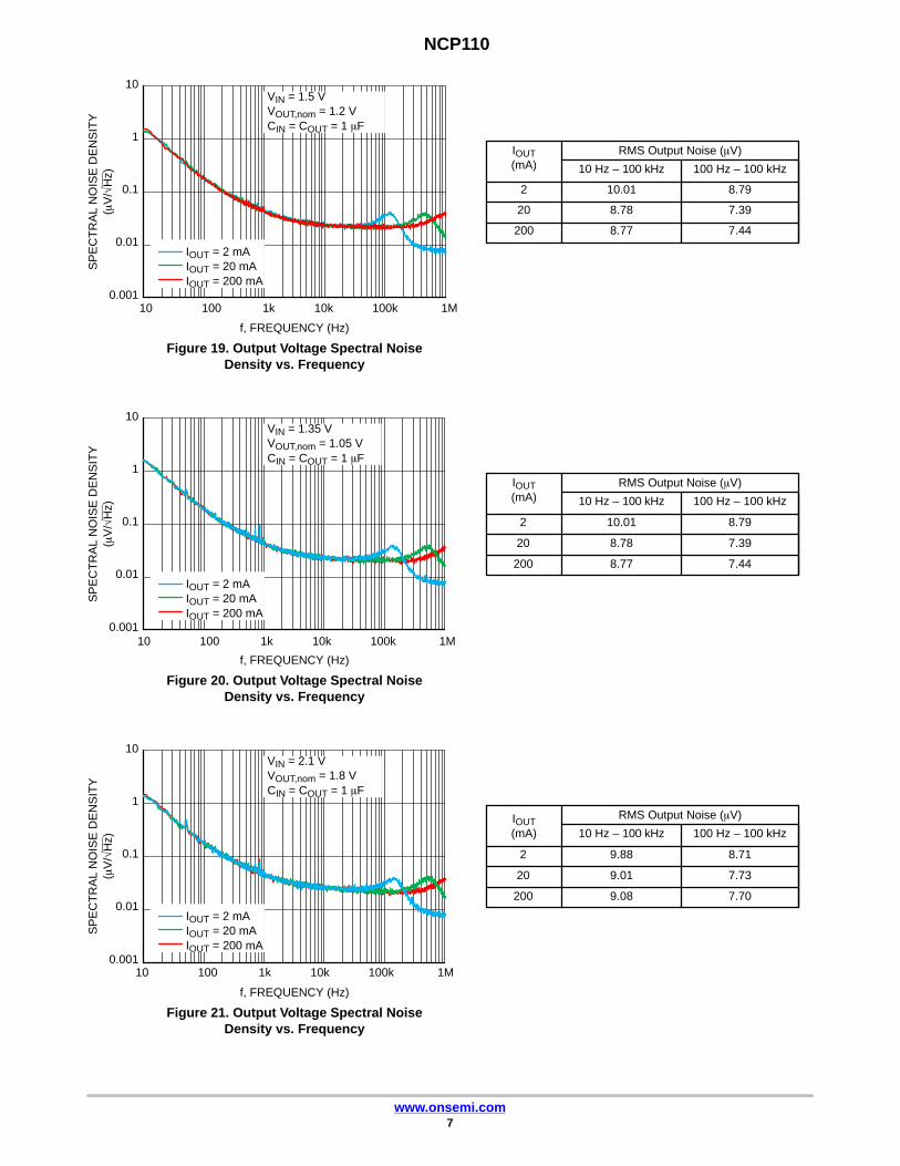
IOUT(mA)
RMS Output Noise (�V)
10 Hz – 100 kHz 100 Hz – 100 kHz
2 10.01 8.79
20 8.78 7.39
200 8.77 7.44
IOUT = 2 mAIOUT = 20 mAIOUT = 200 mA
SP
EC
TR
AL
NO
ISE
DE
NS
ITY
(�V
/√H
z )
f, FREQUENCY (Hz)
Figure 19. Output Voltage Spectral NoiseDensity vs. Frequency
10
10
1
0.1
0.01
0.001100 1k 10k 100k 1M
VIN = 1.5 VVOUT,nom = 1.2 VCIN = COUT = 1 �F
IOUT(mA)
RMS Output Noise (�V)
10 Hz – 100 kHz 100 Hz – 100 kHz
IOUT = 2 mAIOUT = 20 mAIOUT = 200 mA
SP
EC
TR
AL
NO
ISE
DE
NS
ITY
(�V
/√H
z )
f, FREQUENCY (Hz)
Figure 20. Output Voltage Spectral NoiseDensity vs. Frequency
10
1
0.1
0.01
0.001
VIN = 1.35 VVOUT,nom = 1.05 VCIN = COUT = 1 �F
2
20
200
10.01
8.78
8.77
8.79
7.39
7.44
10 100 1k 10k 100k 1M
IOUT(mA)
RMS Output Noise (�V)
10 Hz – 100 kHz 100 Hz – 100 kHz
IOUT = 2 mAIOUT = 20 mAIOUT = 200 mA
SP
EC
TR
AL
NO
ISE
DE
NS
ITY
(�V
/√H
z )
f, FREQUENCY (Hz)
Figure 21. Output Voltage Spectral NoiseDensity vs. Frequency
10
1
0.1
0.01
0.001
VIN = 2.1 VVOUT,nom = 1.8 VCIN = COUT = 1 �F
2
20
200
9.88
9.01
9.08
8.71
7.73
7.70
10 100 1k 10k 100k 1M

NCP110
www.onsemi.com8
TYPICAL CHARACTERISTICSP
SR
R, P
OW
ER
SU
PP
LY R
EJE
CT
ION
RA
TIO
(dB
)
f, FREQUENCY (Hz)
Figure 22. PSRR vs. Frequency
10
120
100 1k 10k 100k 1M 10M
100
80
60
40
20
0
IOUT = 2 mAIOUT = 20 mAIOUT = 200 mA
VIN = 1.35 V + 100 mVppVOUT,nom = 1.05 VCOUT = 1 �F
PS
RR
, PO
WE
R S
UP
PLY
RE
JEC
TIO
NR
AT
IO (
dB)
f, FREQUENCY (Hz)
Figure 23. PSRR vs. Frequency
120
100
80
60
40
20
0
IOUT = 2 mAIOUT = 20 mAIOUT = 200 mA
VIN = 1.5 V + 100 mVppVOUT,nom = 1.2 VCOUT = 1 �F
10 100 1k 10k 100k 1M 10M
PS
RR
, PO
WE
R S
UP
PLY
RE
JEC
TIO
NR
AT
IO (
dB)
f, FREQUENCY (Hz)
Figure 24. PSRR vs. Frequency
120
100
80
60
40
20
0
IOUT = 2 mAIOUT = 20 mAIOUT = 200 mA
VIN = 2.1 V + 100 mVppVOUT,nom = 1.8 VCOUT = 1 �F
10 100 1k 10k 100k 1M 10M

NCP110
www.onsemi.com9
TYPICAL CHARACTERISTICS
VEN
IIN
VOUT
VIN = 1.5 VVOUT,nom = 1.2 VIOUT = 10 mACIN = 1 �FCOUT = 4.7 �F
Figure 25. Enable Turn−on Response,COUT = 1 �F, IOUT = 10 mA
VEN
IIN
VOUT
VIN = 1.5 VVOUT,nom = 1.2 VIOUT = 10 mACIN = COUT = 1 �F
Figure 26. Enable Turn−on Response,COUT = 4.7 �F, IOUT = 10 mA
1 V
/div
100
mA
/div
400
mV
/div
1 V
/div
100
mA
/div
400
mV
/div
20 �s/div 20 �s/div
VIN = 1.5 VVOUT,nom = 1.2 VIOUT = 200 mACIN = COUT = 1 �F
VEN
IIN
VOUT
Figure 27. Enable Turn−on Response,COUT = 1 �F, IOUT = 200 mA
Figure 28. Enable Turn−on Response,COUT = 4.7 �F, IOUT = 200 mA
VEN
IIN
VOUT
VIN = 1.5 VVOUT,nom = 1.2 VIOUT = 200 mACIN = 1 �FCOUT = 4.7 �F
1 V
/div
100
mA
/div
400
mV
/div
1 V
/div
100
mA
/div
400
mV
/div
20 �s/div 20 �s/div
VOUT
VIN
1.5 V
2.5 V
tRISE = 1 �s
tFALL = 1 �s
VOUT,nom = 1.2 VIOUT = 10 mACOUT = 1 �F
Figure 29. Line Transient Response,IOUT = 10 mA
Figure 30. Line Transient Response,IOUT = 200 mA
VIN tRISE = 1 �s
VOUT,nom = 1.2 VIOUT = 200 mACOUT = 1 �F
VOUT
1.5 V2.5 V
tFALL = 1 �s
500
mV
/div
10 m
V/d
iv
500
mV
/div
10 m
V/d
iv
4 �s/div 4 �s/div

NCP110
www.onsemi.com10
TYPICAL CHARACTERISTICS
VOUT
IOUT
tRISE = 1 �s1 mA
200 mA
VIN = 1.5 VVOUT,nom = 1.2 V
COUT = 1 �F
COUT = 4.7 �F
Figure 31. Load Transient Response,IOUT = 1 mA to 200 mA
Figure 32. Load Transient Response,IOUT = 1 mA to 200 mA
VOUT
IOUT tFALL = 1 �s
1 mA
200 mA
VIN = 1.5 VVOUT,nom = 1.2 V
COUT = 1 �F
COUT = 4.7 �F
20 m
V/d
iv10
0 m
A/d
iv
100
mA
/div
20 m
V/d
iv
1 �s/div 10 �s/div
tRISE = 500 ns
tRISE = 1 �s
200 mA
IOUT
1 mA
VOUT
VIN = 1.5 VVOUT,nom = 1.2 VCOUT = 1 �F
Figure 33. Load Transient Response,IOUT = 1 mA to 200 mA
Figure 34. Load Transient Response,IOUT = 1 mA to 200 mA
tRISE = 500 ns
tRISE = 1 �s
200 mA
IOUT
1 mA
VIN = 1.5 VVOUT,nom = 1.2 VCOUT = 1 �F
VOUT
20 m
V/d
iv10
0 m
A/d
iv
20 m
V/d
iv10
0 m
A/d
iv
1 �s/div 4 �s/div
Figure 35. Overheating Protection − TSD
IOUT
VOUT
VIN = 5.5 VVOUT,nom = 1.2 VIOUT = 200 mACIN = 1 �FCOUT = 1 �F
Figure 36. Turn On/Off, Slow Rising VIN
VIN
VOUT
VIN = 0 V to 1.5 VVOUT,nom = 1.2 VIOUT = 10 mACIN = COUT = 1 �F
1.5 V
0 V
400
mV
/div
50 m
A/d
iv
400
mV
/div
100 ms/div 2 ms/div
NCP110
www.onsemi.com11
TYPICAL CHARACTERISTICS
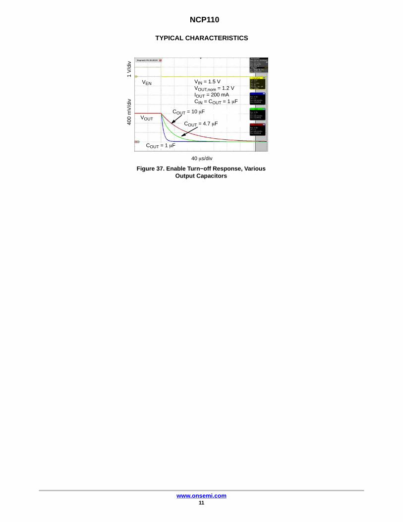
Figure 37. Enable Turn−off Response, VariousOutput Capacitors
VEN VIN = 1.5 VVOUT,nom = 1.2 VIOUT = 200 mACIN = COUT = 1 �F
COUT = 1 �F
COUT = 4.7 �F
COUT = 10 �FVOUT
1 V
/div
400
mV
/div
40 �s/div

NCP110
www.onsemi.com12
APPLICATIONS INFORMATION
GeneralThe NCP110 is an ultra−low input voltage, ultra−low
noise 200 mA low dropout regulator designed to meet therequirements of low voltage RF applications and highperformance analog circuits. The NCP110 device providesvery high PSRR and excellent dynamic response. Inconnection with low quiescent current this device is wellsuitable for battery powered application such as cell phones,tablets and other. The NCP110 is fully protected in case ofcurrent overload, output short circuit and overheating.
Input Capacitor Selection (CIN)Input capacitor connected as close as possible is necessary
for ensure device stability. The X7R or X5R capacitorshould be used for reliable performance over temperaturerange. The value of the input capacitor should be 1 �F orgreater to ensure the best dynamic performance. Thiscapacitor will provide a low impedance path for unwantedAC signals or noise modulated onto constant input voltage.There is no requirement for the ESR of the input capacitorbut it is recommended to use ceramic capacitors for their lowESR and ESL. A good input capacitor will limit theinfluence of input trace inductance and source resistanceduring sudden load current changes.
Output decouplingThe NCP110 requires an output capacitor connected as
close as possible to the output pin of the regulator. Therecommended capacitor value is 1�F and X7R or X5Rdielectric due to its low capacitance variations over thespecified temperature range. The NCP110 is designed toremain stable with minimum effective capacitance of 0.6�Fto account for changes with temperature, DC bias andpackage size. Especially for small package size capacitorssuch as 0201 the effective capacitance drops rapidly with theapplied DC bias. Please refer to Figure 38.
Figure 38. Capacity vs DC Bias Voltage
There is no requirement for the minimum value ofEquivalent Series Resistance (ESR) for the COUT but themaximum value of ESR should be less than 1.6 �. Larger
output capacitors and lower ESR could improve the loadtransient response or high frequency PSRR. It is notrecommended to use tantalum capacitors on the output dueto their large ESR. The equivalent series resistance oftantalum capacitors is also strongly dependent on thetemperature, increasing at low temperature.
Enable OperationThe NCP110 uses the EN pin to enable/disable its device
and to deactivate/activate the active discharge function. Ifthe EN pin voltage is <0.2 V the device is guaranteed to bedisabled. The pass transistor is turned−off so that there isvirtually no current flow between the IN and OUT. Theactive discharge transistor is active so that the output voltageVOUT is pulled to GND through a 280 � resistor. In thedisable state the device consumes as low as typ. 10 nA fromthe VIN. If the EN pin voltage >0.7 V the device isguaranteed to be enabled. The NCP110 regulates the outputvoltage and the active discharge transistor is turned−off. TheEN pin has internal pull−down current source with typ. valueof 200 nA which assures that the device is turned−off whenthe EN pin is not connected. In the case where the ENfunction isn’t required the EN should be tied directly to IN.
Output Current LimitOutput Current is internally limited within the IC to a
typical 350 mA. The NCP110 will source this amount ofcurrent measured with a voltage drops on the 90% of thenominal VOUT. If the Output Voltage is directly shorted toground (VOUT = 0 V), the short circuit protection will limitthe output current to 360 mA (typ). The current limit andshort circuit protection will work properly over wholetemperature range and also input voltage range. There is nolimitation for the short circuit duration.
Thermal ShutdownWhen the die temperature exceeds the Thermal Shutdown
threshold (TSD − 160°C typical), Thermal Shutdown eventis detected and the device is disabled. The IC will remain inthis state until the die temperature decreases below theThermal Shutdown Reset threshold (TSDU − 140°Ctypical). Once the IC temperature falls below the 140°C theLDO is enabled again. The thermal shutdown featureprovides the protection from a catastrophic device failuredue to accidental overheating. This protection is notintended to be used as a substitute for proper heat sinking.
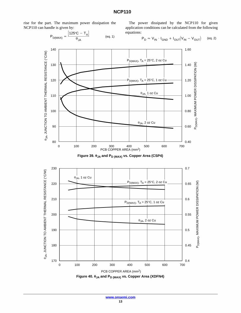
Power DissipationAs power dissipated in the NCP110 increases, it might
become necessary to provide some thermal relief. Themaximum power dissipation supported by the device isdependent upon board design and layout. Mounting padconfiguration on the PCB, the board material, and theambient temperature affect the rate of junction temperature
NCP110
www.onsemi.com13
rise for the part. The maximum power dissipation theNCP110 can handle is given by:
PD(MAX) ��125oC � TA
��JA
(eq. 1)
The power dissipated by the NCP110 for givenapplication conditions can be calculated from the followingequations:
PD � VIN � IGND � IOUTVIN � VOUT
(eq. 2)
0.40
0.60
0.80
1.00
1.20
1.40
1.60
80
90
100
110
120
130
140
0 100 200 300 400 500 600 700
Figure 39. �JA and PD (MAX) vs. Copper Area (CSP4)
PCB COPPER AREA (mm2)
�JA
, JU
NC
TIO
N T
O A
MB
IEN
T T
HE
RM
AL
RE
SIS
TAN
CE
(°C
/W)
PD
(MA
X),
MA
XIM
UM
PO
WE
R D
ISS
IPA
TIO
N (
W)
�JA, 2 oz Cu
�JA, 1 oz Cu
PD(MAX), TA = 25°C, 1 oz Cu
PD(MAX), TA = 25°C, 2 oz Cu
0.4
0.45
0.5
0.55
0.6
0.65
0.7
170
180
190
200
210
220
230
0 100 200 300 400 500 600 700
Figure 40. �JA and PD (MAX) vs. Copper Area (XDFN4)PCB COPPER AREA (mm2)
�JA
, JU
NC
TIO
N T
O A
MB
IEN
T T
HE
RM
AL
RE
SIS
TAN
CE
(°C
/W)
PD
(MA
X),
MA
XIM
UM
PO
WE
R D
ISS
IPA
TIO
N (
W)
�JA, 1 oz Cu
�JA, 2 oz Cu
PD(MAX), TA = 25°C, 1 oz Cu
PD(MAX), TA = 25°C, 2 oz Cu

NCP110
www.onsemi.com14
ORDERING INFORMATION
Device
NominalOutputVoltage Marking Rotation Description Package Shipping†
NCP110AFCT060T2G 0.60 V C 0°
200 mA, Active DischargeWLCSP4
CASE 567VS(Pb-Free)
5000 /Tape &Reel
NCP110AFCT080T2G 0.80 V J 0°
NCP110AFCT085T2G 0.85 V 2 0°
NCP110AFCT100T2G 1.00 V T 0°
NCP110AFCT105T2G 1.05 V A 0°
NCP110AFCT110T2G 1.10 V G 0°
NCP110AFCT120T2G 1.20 V F 0°
NCP110AFCT180T2G 1.80 V D 0°
NCP110AFCT280T2G 2.80 V E 0°
ORDERING INFORMATION
Device Nominal Output Voltage Marking Description Package Shipping
NCP110AMX060TBG 0.60 V FC
200 mA, Active DischargeXDFN4
CASE 711AJ(Pb-Free)
3000 /Tape &Reel
NCP110AMX075TBG 0.75 V F3
NCP110AMX080TBG 0.80 V FJ
NCP110AMX085TBG 0.85 V F2
NCP110AMX100TBG 1.00 V FG
NCP110AMX105TBG 1.05 V FA
NCP110AMX110TBG 1.10 V FH
NCP110AMX120TBG 1.20 V FF
NCP110AMX180TBG 1.80 V FD
NCP110AMX280TBG 2.80 V FE
†For information on tape and reel specifications, including part orientation and tape sizes, please refer to our Tape and Reel PackagingSpecifications Brochure, BRD8011/D.
NCP110
www.onsemi.com15
PACKAGE DIMENSIONS
WLCSP4, 0.64x0.64x0.33CASE 567VS
ISSUE O
ÈÈ
SEATINGPLANE
NOTES:1. DIMENSIONING AND TOLERANCING PER
ASME Y14.5M, 1994.2. CONTROLLING DIMENSION: MILLIMETERS.3. COPLANARITY APPLIES TO SPHERICAL
CROWNS OF SOLDER BALLS.
DIMA
MIN NOM−−−
MILLIMETERS
A1
DE
b 0.180 0.200
e 0.35 BSC
−−−
E
D
A BPIN A1
REFERENCE
e
A0.03 BC
0.05 C
4X b
1 2
B
A
0.05 C
A
A1
A2
C
0.04 0.06TOP VIEW
SIDE VIEW
BOTTOM VIEW
NOTE 3
e
A2 0.23 REF
PITCH 0.204X
DIMENSIONS: MILLIMETERS
*For additional information on our Pb−Free strategy and solderingdetails, please download the ON Semiconductor Soldering andMounting Techniques Reference Manual, SOLDERRM/D.
SOLDERING FOOTPRINT*
0.350.35
RECOMMENDED
A1 PACKAGEOUTLINE
PITCH
MAX
0.610 0.6400.610 0.640
0.220
0.330.08
0.6700.670

NCP110
www.onsemi.com16
PACKAGE DIMENSIONS
XDFN4 1.0x1.0, 0.65PCASE 711AJ
ISSUE A
NOTES:1. DIMENSIONING AND TOLERANCING PER
ASME Y14.5M, 1994.2. CONTROLLING DIMENSION: MILLIMETERS.3. DIMENSION b APPLIES TO PLATED TERMINAL
AND IS MEASURED BETWEEN 0.15 AND0.20 mm FROM THE TERMINAL TIPS.
4. COPLANARITY APPLIES TO THE EXPOSEDPAD AS WELL AS THE TERMINALS.
ÉÉÉÉ
AB
E
D
D2
BOTTOM VIEW
b
e
4X
NOTE 3
2X 0.05 C
PIN ONEREFERENCE
TOP VIEW2X 0.05 C
A
A1
(A3)
0.05 C
0.05 C
C SEATINGPLANESIDE VIEW
L4X1 2
DIM MIN MAXMILLIMETERS
A 0.33 0.43A1 0.00 0.05A3 0.10 REFb 0.15 0.25
D 1.00 BSCD2 0.43 0.53E 1.00 BSCe 0.65 BSCL 0.20 0.30
*For additional information on our Pb−Free strategy and solderingdetails, please download the ON Semiconductor Soldering andMounting Techniques Reference Manual, SOLDERRM/D.
MOUNTING FOOTPRINT*
1.20
0.260.24 4X
DIMENSIONS: MILLIMETERS
0.39
RECOMMENDED
PACKAGEOUTLINE
NOTE 4
e/2
D245 �
AM0.05 BC
4 3
0.65PITCH
DETAIL A
4X
b2 0.02 0.12
L2 0.07 0.17
4X
0.522X
0.114X
L24X
DETAIL A
b24X
ON Semiconductor and are trademarks of Semiconductor Components Industries, LLC dba ON Semiconductor or its subsidiaries in the United States and/or other countries.ON Semiconductor owns the rights to a number of patents, trademarks, copyrights, trade secrets, and other intellectual property. A listing of ON Semiconductor’s product/patentcoverage may be accessed at www.onsemi.com/site/pdf/Patent−Marking.pdf. ON Semiconductor reserves the right to make changes without further notice to any products herein.ON Semiconductor makes no warranty, representation or guarantee regarding the suitability of its products for any particular purpose, nor does ON Semiconductor assume any liabilityarising out of the application or use of any product or circuit, and specifically disclaims any and all liability, including without limitation special, consequential or incidental damages.Buyer is responsible for its products and applications using ON Semiconductor products, including compliance with all laws, regulations and safety requirements or standards,regardless of any support or applications information provided by ON Semiconductor. “Typical” parameters which may be provided in ON Semiconductor data sheets and/orspecifications can and do vary in different applications and actual performance may vary over time. All operating parameters, including “Typicals” must be validated for each customerapplication by customer’s technical experts. ON Semiconductor does not convey any license under its patent rights nor the rights of others. ON Semiconductor products are notdesigned, intended, or authorized for use as a critical component in life support systems or any FDA Class 3 medical devices or medical devices with a same or similar classificationin a foreign jurisdiction or any devices intended for implantation in the human body. Should Buyer purchase or use ON Semiconductor products for any such unintended or unauthorizedapplication, Buyer shall indemnify and hold ON Semiconductor and its officers, employees, subsidiaries, affiliates, and distributors harmless against all claims, costs, damages, andexpenses, and reasonable attorney fees arising out of, directly or indirectly, any claim of personal injury or death associated with such unintended or unauthorized use, even if suchclaim alleges that ON Semiconductor was negligent regarding the design or manufacture of the part. ON Semiconductor is an Equal Opportunity/Affirmative Action Employer. Thisliterature is subject to all applicable copyright laws and is not for resale in any manner.
PUBLICATION ORDERING INFORMATIONN. American Technical Support: 800−282−9855 Toll FreeUSA/Canada
Europe, Middle East and Africa Technical Support:Phone: 421 33 790 2910
NCP110/D
LITERATURE FULFILLMENT:Literature Distribution Center for ON Semiconductor19521 E. 32nd Pkwy, Aurora, Colorado 80011 USAPhone: 303−675−2175 or 800−344−3860 Toll Free USA/CanadaFax: 303−675−2176 or 800−344−3867 Toll Free USA/CanadaEmail: [email protected]
ON Semiconductor Website: www.onsemi.com
Order Literature: http://www.onsemi.com/orderlit
For additional information, please contact your localSales Representative
◊