Embed Size (px)
Citation preview
Digital Link AccessoriesHardware Manual
Keep all product manuals as a product component during the life span of the product. Pass all product manuals to future users/owners of the product.
Version 2.0Catalog No. M.3000.0343Part No. M.3000.1048R1
IND. CONT. EQ.89X2

Record of Revisions
Third party brands and trademarks are the property of their respective owners
Technical changes to improve the performance of the equipment may be made without notice!Printed in USA All rights reserved. No part of this work may be reproduced in any form (by printing, photocopying, microfilm or any othermethod) or processed, copied or distributed by electronic means without the written permission of Kollmorgen.
Edition Valid for Description
08/2010 PiCPro V18.0 Slice I/O Release01/2011 PiCPro V18.0 SP1 DL-DIU Release05/2011 PiCPro V18.0 SP1 Added AT2-R833 Slice I/O Coupler
Kollmorgen - April 2010 1

2
NOTE
These products are being manufactured and sold by G & L Motion Control, Inc., a Kollmorgen company.
Progress is an on-going commitment at Kollmorgen. We continually strive to offer the most advanced products in the industry; therefore, information in this document is subject to change without notice. The text and illustrations are not binding in detail. Kollmorgen shall not be liable for any technical or editorial omissions occurring in this document, nor for any consequential or incidental damages resulting from the use of this document.
Kollmorgen makes every attempt to ensure accuracy and reliability of the specifications in this publication. Specifications are subject to change without notice. Kollmorgen provides this information “AS IS” and disclaims all warranties, express or implied, including, but not limited to, implied warranties of merchantability and fitness for a particular purpose. It is the responsibility of the product user to determine the suitability of this product for a specific application.
DO NOT ATTEMPT to use any Kollmorgen product until the use of such product is completely understood. It is the responsibility of the user to make certain proper operation practices are understood. Kollmorgen products should be used only by qualified personnel and for the express purpose for which said products were designed.
Should information not covered in this document be required, contact the Customer Service Department, Kollmorgen, 672 South Military Road, P.O. Box 1960, Fond du Lac, WI 54936-1960. Kollmorgen can be reached by telephone at (920) 921-7100 or (800) 558-4808 in the United States or by e-mail at [email protected].
Catalog No. (Order No.) M.3000.0343
Printed Version Part No. M.3000.1048R1
Electronic Version Part No. M.3000.1047R1
Release 05232011
©2011, Kollmorgen
Kollmorgen - April 2010

Digital Link Accessories Hardware Manual - TABLE OF CONTENTS
Table of Contents Table of Contents................................................................................................................................3
1 Introduction to Digital Link Accessories .......................................................................................5 1.1 Overview...................................................................................................................................5 1.2 Contents of This Manual...........................................................................................................5 1.3 Software and Manuals..............................................................................................................5
1.3.1 Required Software and Manuals.....................................................................................5 1.3.2 Suggested Manuals ........................................................................................................5
1.4 Kollmorgen Support Contact ....................................................................................................6
2 Safety Precautions...........................................................................................................................7 2.1 System Safety ..........................................................................................................................7
2.1.1 User Responsibility .........................................................................................................7 2.1.2 Safety Instructions...........................................................................................................7
2.2 Safety Signs .............................................................................................................................8 2.3 Warning Labels.........................................................................................................................8 2.4 Safety First ...............................................................................................................................9 2.5 Safety Inspection ......................................................................................................................9
2.5.1 Before Starting System ...................................................................................................9 2.6 After Shutdown .........................................................................................................................9 2.7 Operating Safely.....................................................................................................................10 2.8 Electrical Service & Maintenance Safety................................................................................10 2.9 Safe Cleaning Practices .........................................................................................................11
3 Slice I/O...........................................................................................................................................13 3.1 Introduction.............................................................................................................................13 3.2 Features .................................................................................................................................13 3.3 Overview.................................................................................................................................13 3.4 Slice I/O Coupler Major Components .....................................................................................13 3.5 Power Supply Requirements ..................................................................................................15
3.5.1 System Power ...............................................................................................................15 3.5.2 Field Power ...................................................................................................................15 3.5.3 Non-24Vdc Field Power ................................................................................................15
3.6 Module Installation..................................................................................................................16 3.6.1 DIN Rail Installation.......................................................................................................16 3.6.2 Slice I/O Coupler Installation.........................................................................................16 3.6.3 Slice I/O Module Installation..........................................................................................17
3.7 Module Removal.....................................................................................................................17 3.7.1 Slice I/O Coupler Removal............................................................................................17 3.7.2 Slice I/O Module Removal.............................................................................................18
3.8 Removable Terminal Block Operation....................................................................................18 3.9 Slice I/O Coupler Details ........................................................................................................19
3.9.1 LED Indicators...............................................................................................................19 3.9.2 Node Address Rotary Switches) ...................................................................................20 3.9.3 Digital Link Ports ...........................................................................................................21 3.9.4 Power Input Connector .................................................................................................23 3.9.5 DC Input Connectors.....................................................................................................24 3.9.6 DC Output Connectors..................................................................................................26 3.9.7 Slice I/O Coupler Wiring Examples ...............................................................................27
3.10 Slice I/O Modules .................................................................................................................30 3.10.1 Slice I/O Limitations and Precautions .........................................................................30
Kollmorgen - April 2010 3
4
Digital Link Accessories Hardware Manual - TABLE OF CONTENTS
3.10.2 Slice I/O Modules ....................................................................................................... 30 3.11 Slice I/O Coupler Specifications........................................................................................... 35
4 Digital Link Drive Interface Unit ................................................................................................... 37 4.1 DL-DIU Front Panel Details.................................................................................................... 39
4.1.1 LED Indicators .............................................................................................................. 39 4.1.2 Power Indicator Details................................................................................................. 39 4.1.3 Diagnostic Indicator Details .......................................................................................... 39 4.1.4 Digital Link LEDs .......................................................................................................... 39 4.1.5 Node Address Rotary Switches.................................................................................... 40 4.1.6 Digital Link Ports........................................................................................................... 41 4.1.7 Axis I/O Port ................................................................................................................. 43
4.1.7.1 Axis I/O Port DC Outputs .................................................................................... 47 4.1.7.2 Axis I/O Port DC Input......................................................................................... 49 4.1.7.3 Axis I/O Port Analog Output ................................................................................ 50 4.1.7.4 Axis I/O Port Encoder Input................................................................................. 51
4.1.8 I/O and Power Ports ..................................................................................................... 52 4.1.9 I/O Port Details ............................................................................................................. 54
4.1.9.1 I/O Port Input....................................................................................................... 54 4.1.9.2 Analog Input ........................................................................................................ 55 4.1.9.3 I/O Port Wiring Example...................................................................................... 55
4.2 Specifications ......................................................................................................................... 57
5 CE and EMC Guidelines................................................................................................................ 61 5.1 Background on EMC (Electromagnetic Compatibility) Compliance ....................................... 61 5.2 Background on Low Voltage Compliance .............................................................................. 61 5.3 RFI Emission and Immunity ................................................................................................... 61 5.4 Classes of EMC Operating Environments.............................................................................. 62 5.5 Conformance with the EMC Directive .................................................................................... 63 5.6 Conformance With the Low Voltage Directive........................................................................ 63 5.7 Changes to the PiC Products................................................................................................. 63
5.7.1 Changes Affecting the User.......................................................................................... 63 5.8 Using CE/EMC and Non-CE/EMC Modules .......................................................................... 66 5.9 Declarations of Conformity..................................................................................................... 68
Appendix A - Operation Details....................................................................................................... 73 6.1 Introduction ............................................................................................................................ 73 6.2 DC Inputs ............................................................................................................................... 73 6.3 DC Outputs ............................................................................................................................ 74
6.3.1 Inductive Loads ............................................................................................................ 74 6.4 Encoder Inputs ....................................................................................................................... 75
Index .................................................................................................................................................. 77
Sales and Service ............................................................................................................................. 80
Kollmorgen - April 2010

Digital Link Accessories Hardware Manual - INTRODUCTION TO DIGITAL LINK ACCESSORIES
1 Introduction to Digital Link Accessories1.1 Overview
This manual covers all products that reside on the Digital Link communication network, but that are neither Controls nor Drives.
1.2 Contents of This ManualThis manual includes the following major topics:
• Information to safely operate and maintain the equipment in a safe manner.
• User responsibilities for product acceptance and storage.
• Power and environmental information for general power, control cabinet, ground-ing, heat control and handling.
• Procedures for mounting, wiring, and connecting the Accessories to the control system.
• Recommended system wiring guidelines for signal separation, differential devices, and to ensure ElectroMagnetic Compatibility.
• The location of connectors on the Accessory and descriptions of their functional-ity.
• Physical, electrical, environmental and functional specifications/dimensions.
• Description of the minimal maintenance necessary.
• A troubleshooting chart of potential problems and possible solutions.
• Part numbers and descriptions for the drive and related equipment.
1.3 Software and Manuals
1.3.1 Required Software and ManualsPiCPro (one of the following)
• Professional Edition
• MMC Limited Edition
• Monitor Edition (Diagnostics Only)
1.3.2 Suggested Manuals
• MMC smart Drive and Digital MMC Control Hardware Manual
• Standalone MMC Hardware Manual
• Function/Function Block Reference Guide
• Motion Application Specific Function Block Manual
• Ethernet Application Specific Function Block Manual
• General Purpose Application Specific Function BlockManual
Kollmorgen - April 2010 5

6
Digital Link Accessories Hardware Manual - INTRODUCTION TO DIGITAL LINK ACCESSORIES
1.4 Kollmorgen Support Contact
Contact your local Kollmorgen representative for:
• Sales and order support
• Product technical training
• Warranty support
• Support service agreements
Kollmorgen Technical Support can be reached:
• In the United States, telephone (800) 558-4808
• Outside the United States, telephone (920) 921-7100
• E-mail address: [email protected]
• Web site: www.kollmorgen.com
Kollmorgen - April 2010

Digital Link Accessories Hardware Manual - SAFETY PRECAUTIONS
2 Safety Precautions
READ AND UNDERSTAND THIS SECTION IN ITS ENTIRETY BEFORE UNDERTAKING INSTALLATION OR ADJUSTMENT OF THE MMC SMART DRIVE AND ANY ASSOCIATED SYSTEMS OR EQUIPMENT
The instructions contained in this section will help users to operate and maintain the equipment in a safe manner.
PLEASE REMEMBER THAT SAFETY IS EVERYONE'S RESPONSIBILITY
2.1 System Safety The basic rules of safety set forth in this section are intended as a guide for the safe operation of equipment. This general safety information, along with explicit service, maintenance and operational materials, make up the complete instruction set. All personnel who operate, service or are involved with this equipment in any way should become totally familiar with this information prior to operating.
2.1.1 User ResponsibilityIt is the responsibility of the user to ensure that the procedures set forth here are followed and, should any major deviation or change in use from the original specifications be required, appropriate procedures should be established for the continued safe operation of the system. It is strongly recommended that you contact your OEM to ensure that the system can be safely converted for its new use and continue to operate in a safe manner.
2.1.2 Safety Instructions
• Do not operate your equipment with safety devices bypassed or covers removed.
• Only qualified personnel should operate the equipment.
• Never perform service or maintenance while automatic control sequences are in operation.
• To avoid shock or serious injury, only qualified personnel should perform mainte-nance on the system.
Kollmorgen - April 2010 7
8
Digital Link Accessories Hardware Manual - SAFETY PRECAUTIONS
• GROUNDING (Protective Earth)
The equipment must be grounded (connected to the protective earth connection) according to OEM recommendations and to the latest local regulations for electrical safety. The grounding (protective earth) conductor must not be interrupted inside or outside the equipment enclosures. The wire used for equipment grounding (connection to protective earth) should be green with a yellow stripe.
2.2 Safety Signs The purpose of a system of safety signs is to draw attention to objects and situations which could affect personal or plant safety. It should be noted that the use of safety signs does not replace the need for appropriate accident prevention measures. Always read and follow the instructions based upon the level of hazard or potential danger.
2.3 Warning LabelsHazard warning
When you see this safety sign on a system, it gives a warning of a hazard or possibility of a hazard existing. The type of warning is given by the pictorial representation on the sign plus text if used.
To ignore such a caution could lead to severe injury or death arising from an unsafe practice.
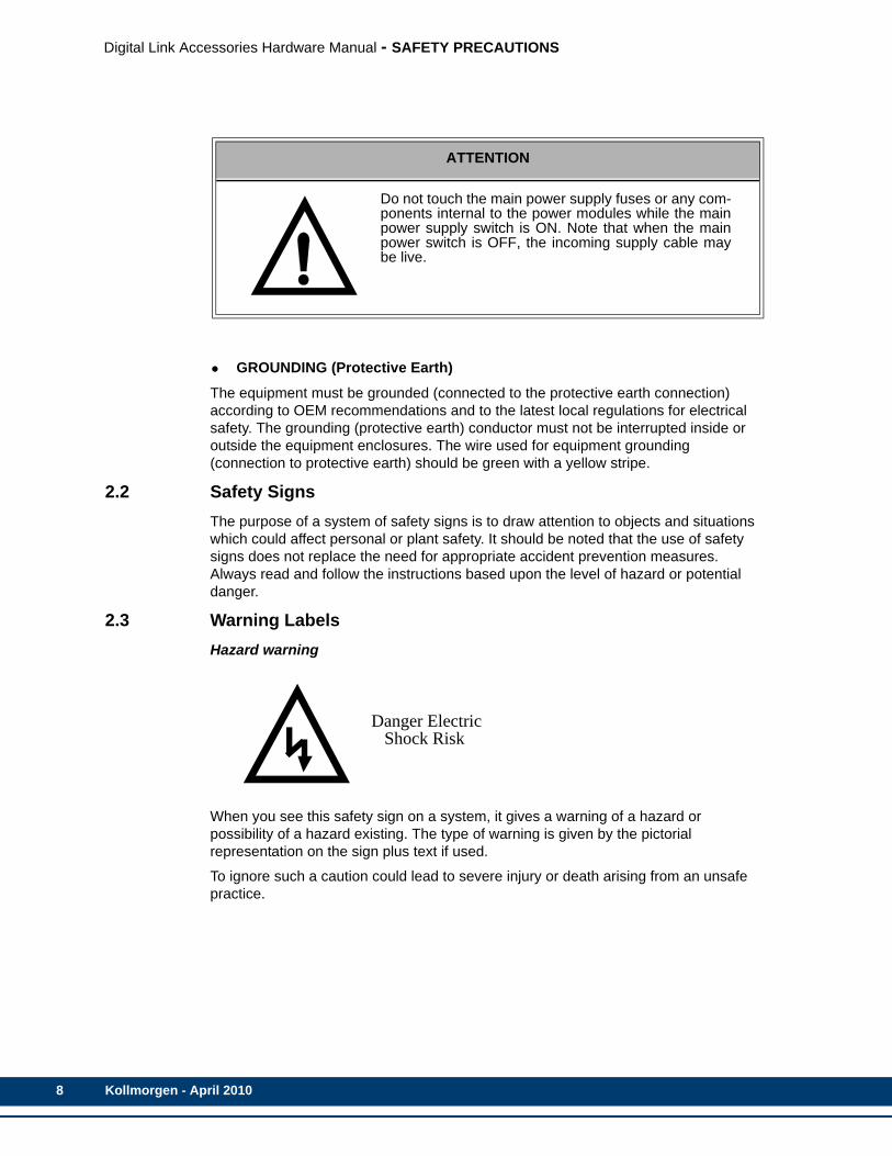
ATTENTION
Do not touch the main power supply fuses or any com-ponents internal to the power modules while the mainpower supply switch is ON. Note that when the mainpower switch is OFF, the incoming supply cable maybe live.
Danger Electric Shock Risk
Kollmorgen - April 2010

Digital Link Accessories Hardware Manual - SAFETY PRECAUTIONS
Danger, Warning, or Caution warning
Hot Surface warning
2.4 Safety FirstKollmorgen equipment is designed and manufactured with consideration and care to generally accepted safety standards. However, the proper and safe performance of the equipment depends upon the use of sound and prudent operating, maintenance and servicing procedures by trained personnel under adequate supervision.
For your protection, and the protection of others, learn and always follow these safety rules. Observe warnings on machines and act accordingly. Form safe working habits by reading the rules and abiding by them. Keep these safety rules handy and review them from time to time to refresh your understanding of them.
2.5 Safety Inspection
2.5.1 Before Starting System
• Ensure that all guards and safety devices are installed and operative and all doors which carry warning labels are closed and locked.
• Ensure that all personnel are clear of those areas indicated as potentially hazard-ous.
• Remove (from the operating zone) any materials, tools or other objects that could cause injury to personnel or damage the system.
• Make sure that the control system is in an operational condition.
• Make certain that all indicating lights, horns, pressure gauges or other safety devices or indicators are in working order.
2.6 After ShutdownMake certain all controlled equipment in the plant is safe and the associated electrical, pneumatic or hydraulic power is turned off. It is permissible for the control equipment contained in enclosures to remain energized provided this does not conflict with the safety instructions found in this section.
Symbol plus DANGER, WARNING or CAUTION: These notices provide information intended to prevent potentialpersonal injury and equipment damage.
Symbol plus HOT SURFACE:These notices provide information intended to prevent potential personal injury.
Kollmorgen - April 2010 9
10
Digital Link Accessories Hardware Manual - SAFETY PRECAUTIONS
2.7 Operating Safely• Do not operate the control system until you read and understand the operating
instructions and become thoroughly familiar with the system and the controls.
• Never operate the control system while a safety device or guard is removed or disconnected
• Where access to the control system is permitted for manual operation, only those doors which provide that access should be unlocked. They should be locked immediately after the particular operation is completed.
• Never remove warnings that are displayed on the equipment. Torn or worn labels should be replaced.
• Do not start the control system until all personnel in the area have been warned.
• Never sit or stand on anything that might cause you to fall onto the control equip-ment or its peripheral equipment.
• Horseplay around the control system and its associated equipment is dangerous and should be prohibited.
• Never operate the equipment outside specification limits.
• Keep alert and observe indicator lights, system messages and warnings that are displayed on the system.
• Do not operate faulty or damaged equipment. Make certain proper service and maintenance procedures have been performed.
2.8 Electrical Service & Maintenance Safety• ALL ELECTRICAL OR ELECTRONIC MAINTENANCE AND SERVICE
SHOULD BE PERFORMED BY TRAINED AND AUTHORIZED PERSONNEL ONLY.
• It should be assumed at all times that the POWER is ON and all conditions treated as live. This practice assures a cautious approach which may prevent accident or injury.
• To remove power:LOCK THE SUPPLY CIRCUIT DISCONNECTING MEANS IN THE OPEN POSI-TION.APPLY LOCKOUT/TAGOUT DEVICES IN ACCORDANCE WITH A DOCU-MENTED AND ESTABLISHED POLICY.
• Make sure the circuit is safe by using the proper test equipment. Check test equip-ment regularly.
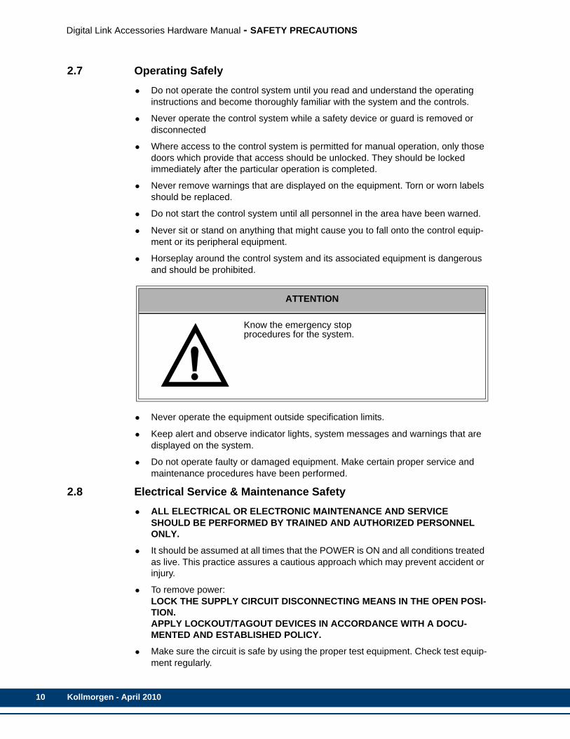
ATTENTION
Know the emergency stop procedures for the system.
Kollmorgen - April 2010
Digital Link Accessories Hardware Manual - SAFETY PRECAUTIONS
• There may be circumstances where troubleshooting on live equipment is required. Under such conditions, special precautions must be taken:
• Make sure your tools and body are clear of the areas of equipment which may be live.
• Extra safety measures should be taken in damp areas.
• Be alert and avoid any outside distractions.
• Make certain another qualified person is in attendance.
• Before applying power to any equipment, make certain that all personnel are clear of associated equipment.
• Control panel doors should be unlocked only when checking out electrical equip-ment or wiring. On completion, close and lock panel doors.
• All covers on junction panels should be fastened closed before leaving any job.
• Never operate any controls while others are performing maintenance on the sys-tem.
• Do not bypass a safety device.
• Always use the proper tool for the job.
• Replace the main supply fuses only when electrical power is OFF (locked out).
2.9 Safe Cleaning Practices• Do not use toxic or flammable solvents to clean control system hardware.
• Turn off electrical power (lock out) before cleaning control system assemblies.
• Keep electrical panel covers closed and power off when cleaning an enclosure.
• Always clean up spills around the equipment immediately after they occur.
• Never attempt to clean a control system while it is operating.
• Never use water to clean control equipment unless you are certain that the equip-ment has been certified as sealed against water ingress. Water is a very good conductor of electricity and the single largest cause of death by electrocution.
Kollmorgen - April 2010 11

12
Digital Link Accessories Hardware Manual - SAFETY PRECAUTIONS
Kollmorgen - April 2010

Digital Link Accessories Hardware Manual - SLICE I/O
3 Slice I/O3.1 Introduction
This section contains information on Kollmorgen’s Slice I/O System of I/O modules. The Slice I/O System allows the user to integrate a variety of Slice I/O modules with any MMC Digital Control via the Digital Link communication interface. Information on Kollmorgen’s line of Digital Controls can be found in the Standalone MMC Hardware Manual, and the MMC Smart Drive and Digital Control Hardware Manual.
3.2 FeaturesThe Slice I/O System provides the following features:
• DIN rail mounting
• Removable Terminal Blocks, which allow the user to replace a Module without unwiring/rewiring the Module. (Note: 16 point DC I/O modules do not contain Removable Terminal Blocks. Refer to Table 3-15 on page 34 for available mating connector.)
• Individual Module replacement. Any Module can be replaced without the need to remove any other Module
• The Slice I/O Coupler, which:
• Provides the interface between the Digital Link communications network and the Slice I/O Modules
• Provides 16 fast inputs (24Vdc), and 16 fast outputs (24Vdc)
• Slice I/O Modules, that provide I/O between the Digital Control and the machine. Slice I/O Modules include the following:
• Digital Input Modules (5Vdc, 12Vdc, 24Vdc, 48Vdc, 110Vac, and 220Vac)
• Digital Output Modules (5Vdc, 24Vdc, 120Vdc, and Relay Out)
• Analog Input Modules (0-20ma, 4-20ma, 0-10Vdc, +/-10Vdc)
• Analog Output Modules (0-20ma, 0-1,000ma, 0-5Vdc, 0-10Vdc, +/-10Vdc)
• Power Supply and Distribution Modules
3.3 OverviewKollmorgen’s Slice I/O System offers a low cost, highly modular solution to system I/O requirements. One Slice I/O Coupler can provide up to 144 input points, and 144 output points, depending on the type of Slice I/O Module installed. Furthermore, a Control System containing a Digital Control can contain from 2 to 64 Slice I/O Couplers, depending on the Control type and other Digital Link devices (typically Kollmorgen Smart Drives) that are installed within the system.
Once properly installed, Slice I/O Input Modules provide machine data to the Application Program, and Slice I/O Output Modules provide machine control from the Application Program. The Application Program is developed using Kollmorgen’s PiCPro integrated Application Development Environment.
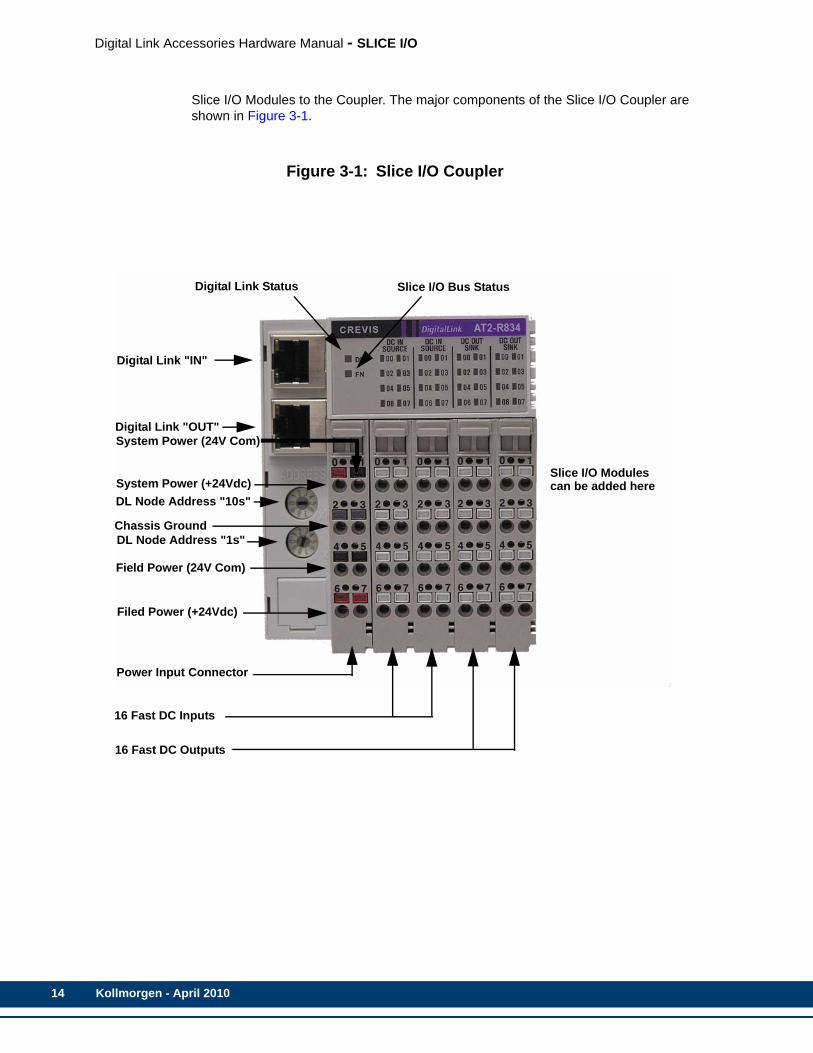
3.4 Slice I/O Coupler Major ComponentsThe Slice I/O Coupler contains the Digital Link "IN" and "OUT" ports, Digital Link node address switches, 16 fast DC Inputs, 16 fast DC Outputs, and an interface for adding
Kollmorgen - April 2010 13
14
Digital Link Accessories Hardware Manual - SLICE I/O
Slice I/O Modules to the Coupler. The major components of the Slice I/O Coupler are shown in Figure 3-1.
Figure 3-1: Slice I/O Coupler
Digital Link "IN"
Digital Link "OUT"
System Power (+24Vdc)
DL Node Address "1s"
Filed Power (+24Vdc)
Field Power (24V Com)
System Power (24V Com)
DL Node Address "10s"
Chassis Ground
Digital Link Status Slice I/O Bus Status
16 Fast DC Outputs
16 Fast DC Inputs
Slice I/O Modulescan be added here
Power Input Connector
Kollmorgen - April 2010
Digital Link Accessories Hardware Manual - SLICE I/O
3.5 Power Supply RequirementsPower to the Slice I/O Coupler is provided by the user via the Input Power Connector, located on the far left of the Coupler as shown in Figure 3-1 on page 14.
The Slice I/O System contains two separate and distinct Power Systems. These Power Systems provide the System Power and the Field Power to the Coupler and Slice I/O modules. Each Power System is described below.
3.5.1 System Power24Vdc (nominal) is provided by the user, and the Slice I/O Coupler converts this to 5Vdc to provide System Power. This 5Vdc supplies the power for the components within the Coupler and the attached Slice I/O modules.
The Coupler can provide a maximum of 1A of 5Vdc power to the attached Slice I/O modules. If the System Power of the attached Slice I/O modules exceeds 1A, an Expansion Power Supply Module (P/N ST-7111) must be installed to provide addition System Power. Refer to the ST-7111 Data Sheet for additional information.
To determine the system System Power requirements, refer to the Data Sheets for all connected Slice I/O Modules for each Module’s System Power current usage. The current usage is listed under "Power Dissipation" in the "General Specifications" section in the Data Sheets.
3.5.2 Field Power24Vdc (nominal) is provided by the user to the Slice I/O Coupler, and the Coupler uses this to power the 16 Fast Inputs and 16 Fast Outputs provided by the Coupler. This 24Vdc is also passed through the Coupler to supply Field Power to any connected 24Vdc Slice I/O Modules.
The Coupler can provide a maximum of 10A of 24Vdc power to power the 16 Inputs and 16 Outputs provided by the Coupler plus the Field Power requirements of the attached Slice I/O modules. If the Field Power required exceeds 10A, an Expansion Field Power Distributor Module (P/N ST-7241) must be installed to provide addition Field Power. Refer to the ST-7241 Data Sheet for additional information.
To determine the system Field Power requirements, refer to the Data Sheets for all connected Slice I/O Modules for each Module’s Field Power current usage. The current usage is listed under "Field Power - Power Dissipation" in the "General Specifications" section in the Data Sheets. Then, add the current requirements of any loads connected to the Slice I/O outputs.
3.5.3 Non-24Vdc Field PowerMany Slice I/O modules require Field Power other than 24Vdc, such as 5Vdc, 48Vdc, 110Vac, or 220Vac. When switching between Field Power voltages, it is absolutely necessary to install an Expansion Field Power Distributor (P/N ST-7241) between the Modules. Refer to the ST-7241 Data Sheet for additional information.
WARNING
Failure to read and understand this section can result in damage to the entireSlice I/O System. This damage will not be covered under Kollmorgen’s war-ranty policy.
Kollmorgen - April 2010 15
16
Digital Link Accessories Hardware Manual - SLICE I/O
3.6 Module InstallationThe Slice I/O Coupler and Slice I/O Modules are mounted to a DIN Rail that is typically mounted to the user’s control panel.
3.6.1 DIN Rail InstallationMount the required length of DIN rail to the panel within the control cabinet. Make sure that the DIN rail makes good electrical connection to the panel, and that the panel is connected to Single Point Ground. When selecting the DIN rail, Kollmorgen has found that the galvanized product exhibits superior performance, especially in the area of noise emission and suppression.
3.6.2 Slice I/O Coupler InstallationMount the Slice I/O Coupler on the left of the DIN rail as follows:
• Make certain that the release lever found at the bottom of the Coupler is in the release position. Do this by inserting a flat-bladed screw driver into the Release Tab, and pushing the handle of the screw driver towards the top of the Coupler (using the bottom of the Coupler as a pivot point) until the Release Tab locks in the Release (out) position. Please note that twisting the screwdriver blade while it is in the Release Tab will not move the Release Tab into the Release position.
• Position the Coupler over the DIN rail, making sure that the back of the Coupler is tight against the panel that the DIN rail is mounted to.
• Press the Coupler Release Lever up towards the Coupler, until it snaps into the "lock" (in) position.
• Make sure that the plastic End Cover that is included with the Coupler is installed on the right side of the Coupler to protect the Slice I/O contact pins.
Slice I/O Coupler dimensions are shown in Figure 3-2 on page 17.
Kollmorgen - April 2010
Digital Link Accessories Hardware Manual - SLICE I/O
Figure 3-2: Slice I/O Coupler Dimensions
3.6.3 Slice I/O Module InstallationMount a Slice I/O Module to the right of the Coupler or another Slice I/O Module as follows:
• Remove the End Cover from the right side of the Slice I/O system that the addi-tional Slice I/O Module(s) is being installed on.
• Make certain that the blue release lever found at the bottom of the Module is in the non-release position by rotating the lever towards the bottom of the Module until it is flush with the bottom of the Module.
• Align the plastic guides located at the top and bottom of the Module with the asso-ciated slots in the previously mounted Module, and slide the Module down towards the DIN rail
• Press the Module firmly onto the DIN rail until it snaps into place
• Re-install the plastic End Cover that was removed in step one on the right side of the installed Module(s) to protect the Slice I/O contact pins.
3.7 Module RemovalThis section describes the steps required to remove the Slice I/O Coupler and a Slice I/O Module from the DIN rail.
3.7.1 Slice I/O Coupler RemovalPerform the following steps to remove a Slice I/O Coupler from the DIN rail:
Kollmorgen - April 2010 17

18
Digital Link Accessories Hardware Manual - SLICE I/O
• If there is a Slice I/O Module attached to the right side of the Coupler, remove it as described in Section 3.7.2 below.
• Locate the Coupler Release Tab located underneath the Coupler
• Insert a flat-bladed screw driver into the Release Tab, and push the handle of the screw driver towards the top of the Coupler (using the bottom of the Coupler as a pivot point) until the Release Tab locks in the Release (out) position. Please note that twisting the screwdriver blade while it is in the Release Tab will not move the Release Tab into the Release position.
• Rock the bottom of the Coupler out of the DIN rail. With the bottom still rocked for-ward, lift the Coupler straight up and off of the DIN rail.
3.7.2 Slice I/O Module RemovalPerform the following steps to remove a Slice I/O Module from the DIN rail:
• Locate the blue Release Tab at the bottom of the Module.
• Using a flat-bladed screwdriver, rotate the Release Tab down and away from the Module until it stays in the Release position, which is at a right angle to the bottom of the Module.
• Slide the Module away form the DIN rail until it is completely separated from the surrounding Module(s).
3.8 Removable Terminal Block OperationConnection between Slice I/O Modules and user equipment is made via Removable Terminal Blocks located on each Module. Removable Terminal Blocks allow the replacement of a Module without the need for unwiring/rewiring.
Note: 16 point DC I/O modules do not contain Removable Terminal Blocks. Refer to Table 3-15 on page 34 for available mating connector.
Terminal block Removal:
• Pull the Terminal Block Release Tab, located at the top of the Terminal Block, until the Terminal Block rocks forward and out of the Module.
Terminal Block Insertion:
• Before inserting the Terminal Block into the Module, push the Terminal Block Release Tab, located at the top of the Terminal Block, all the way in to the "lock" position.
• Hook the bottom of the Terminal Block into the Module
• Rock the top of Terminal Block forward until it snaps into the Module
Terminal Block Wiring:
• Use wire up to 14AWG
• Strip .25in (6.35mm) of insulation from the end of the wire
• Using a small flat-bladed screwdriver, depress the Wire Release Tab above the desired terminal
• Insert the previously-strip wire into the terminal hole
• Release the Wire Release Tab
Kollmorgen - April 2010

Digital Link Accessories Hardware Manual - SLICE I/O
3.9 Slice I/O Coupler DetailsThis section describes the Slice I/O Coupler, including the LED Indicators, Connectors, and Operation.
3.9.1 LED IndicatorsThere are 32 LEDs located on the Coupler that indicate the status of the 32 I/O points that are integrated within the Coupler. These LEDs are described in section 3.9.5 on page 24 and section 3.9.6 on page 26.
There two additional LEDs located on the front of the Coupler, as follows:
• The Digital Link Status LED, labeled "DL" on the front of the Coupler as seen in Figure 3-1 on page 14, indicates the status of the communication between the Coupler and the Digital Control. This LED can be in one of three states:
• Off - the Digital Control running the user’s application has not yet initialized the Coupler, or power is not being applied to the Coupler
• Green - the Coupler is initialized and the user’s application is controlling the Coupler. This condition occurs when the Coupler is properly connected to the Digital Control, and the user’s application is running (scanning). When the "DL" LED is green, the user’s application control’s the outputs on the Coupler and all attached Slice I/O Modules.
• Red - the Coupler is initialized and the user’s application is not controlling the Coupler. This condition can occur if the Coupler is disconnected from the Dig-ital Control, or the user’s application is stopped (not scanning). When the "DL" LED is red, all outputs on the Coupler and attached Slice I/O Modules are forced off.
• The Slice I/O Communication Link Status LED, labeled "FN" on the front of the Coupler as seen in Figure 3-1 on page 14, indicates the status of the communica-tion between the Coupler and the attached Slice I/O Modules. This LED can be in one of the following three states:
• Off - The Slice I/O system is not being accessed. All outputs are forced off.
• Green - The slice I/O system is being properly accessed by the application. Outputs are being controlled by the application, and Inputs are being read by the application.
• Red - There has been a communication problem between the Slice I/O Cou-pler and the attached Slice I/O Modules. The outputs on the Coupler continue to be controlled by the user’s application, however, the outputs on all attached Slice I/O modules are forced off.
Kollmorgen - April 2010 19
20
Digital Link Accessories Hardware Manual - SLICE I/O
3.9.2 Node Address Rotary Switches)Two rotary switches are used to set the Digital Link Node address of the Slice I/O Coupler. These are labeled "x10" and "x1" on the front of the Coupler, as seen in Figure 3-1 on page 14. Rotate the switches to the desired address.
Addresses can be set to any number from 1 through 64. The top switch represents values of base ten. The bottom switch represents values of base 1.
As an example, rotating the switch to a setting of 2 on the top switch equals the value of 20 (2 x 10). Rotating the switch on the bottom switch to a setting of 5 equals the value of 5. The actual address setting is 25 (20 + 5).
x10
x1
Address
Kollmorgen - April 2010
Digital Link Accessories Hardware Manual - SLICE I/O
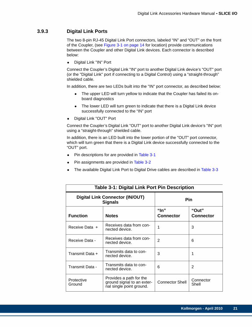
3.9.3 Digital Link PortsThe two 8-pin RJ-45 Digital Link Port connectors, labeled “IN” and “OUT” on the front of the Coupler, (see Figure 3-1 on page 14 for location) provide communications between the Coupler and other Digital Link devices. Each connector is described below:
• Digital Link "IN" Port
Connect the Coupler’s Digital Link "IN" port to another Digital Link device’s "OUT" port (or the "Digital Link" port if connecting to a Digital Control) using a “straight-through” shielded cable.
In addition, there are two LEDs built into the "IN" port connector, as described below:
• The upper LED will turn yellow to indicate that the Coupler has failed its on-board diagnostics
• The lower LED will turn green to indicate that there is a Digital Link device successfully connected to the “IN” port
• Digital Link "OUT" Port
Connect the Coupler’s Digital Link "OUT" port to another Digital Link device’s "IN" port using a “straight-through” shielded cable.
In addition, there is an LED built into the lower portion of the "OUT" port connector, which will turn green that there is a Digital Link device successfully connected to the “OUT” port.
• Pin descriptions for are provided in Table 3-1
• Pin assignments are provided in Table 3-2
• The available Digital Link Port to Digital Drive cables are described in Table 3-3
Table 3-1: Digital Link Port Pin Description
Digital Link Connector (IN/OUT) Signals Pin
Function Notes“In”Connector
“Out” Connector
Receive Data + Receives data from con-nected device. 1 3
Receive Data - Receives data from con-nected device. 2 6
Transmit Data + Transmits data to con-nected device. 3 1
Transmit Data - Transmits data to con-nected device. 6 2
Protective Ground
Provides a path for the ground signal to an exter-nal single point ground.
Connector Shell Connector Shell
Kollmorgen - April 2010 21
22
Digital Link Accessories Hardware Manual - SLICE I/O
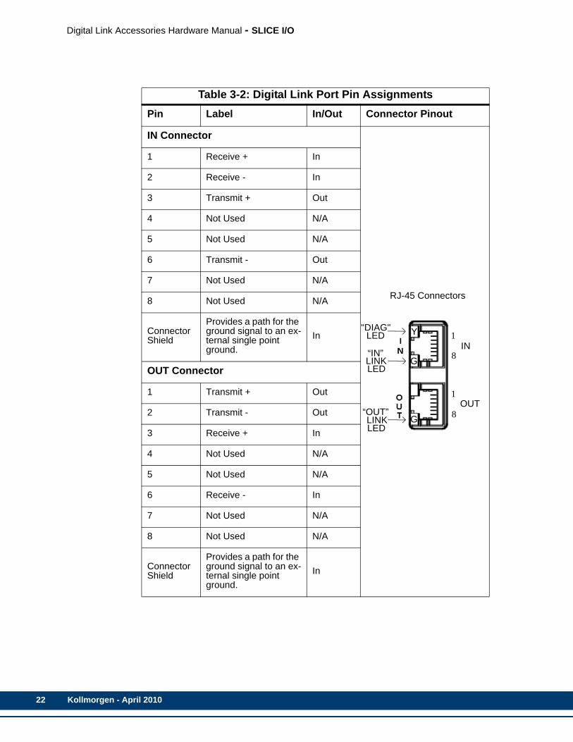
Table 3-2: Digital Link Port Pin AssignmentsPin Label In/Out Connector Pinout
IN Connector
1 Receive + In
RJ-45 Connectors
2 Receive - In
3 Transmit + Out
4 Not Used N/A
5 Not Used N/A
6 Transmit - Out
7 Not Used N/A
8 Not Used N/A
Connector Shield
Provides a path for the ground signal to an ex-ternal single point ground.
In
OUT Connector
1 Transmit + Out
2 Transmit - Out
3 Receive + In
4 Not Used N/A
5 Not Used N/A
6 Receive - In
7 Not Used N/A
8 Not Used N/A
Connector Shield
Provides a path for the ground signal to an ex-ternal single point ground.
In
1
8
1
8
“IN”LINK
“OUT”LINKLED
LED
IN
OUT
"DIAG"LED Y
G
G
Kollmorgen - April 2010

Digital Link Accessories Hardware Manual - SLICE I/O
03
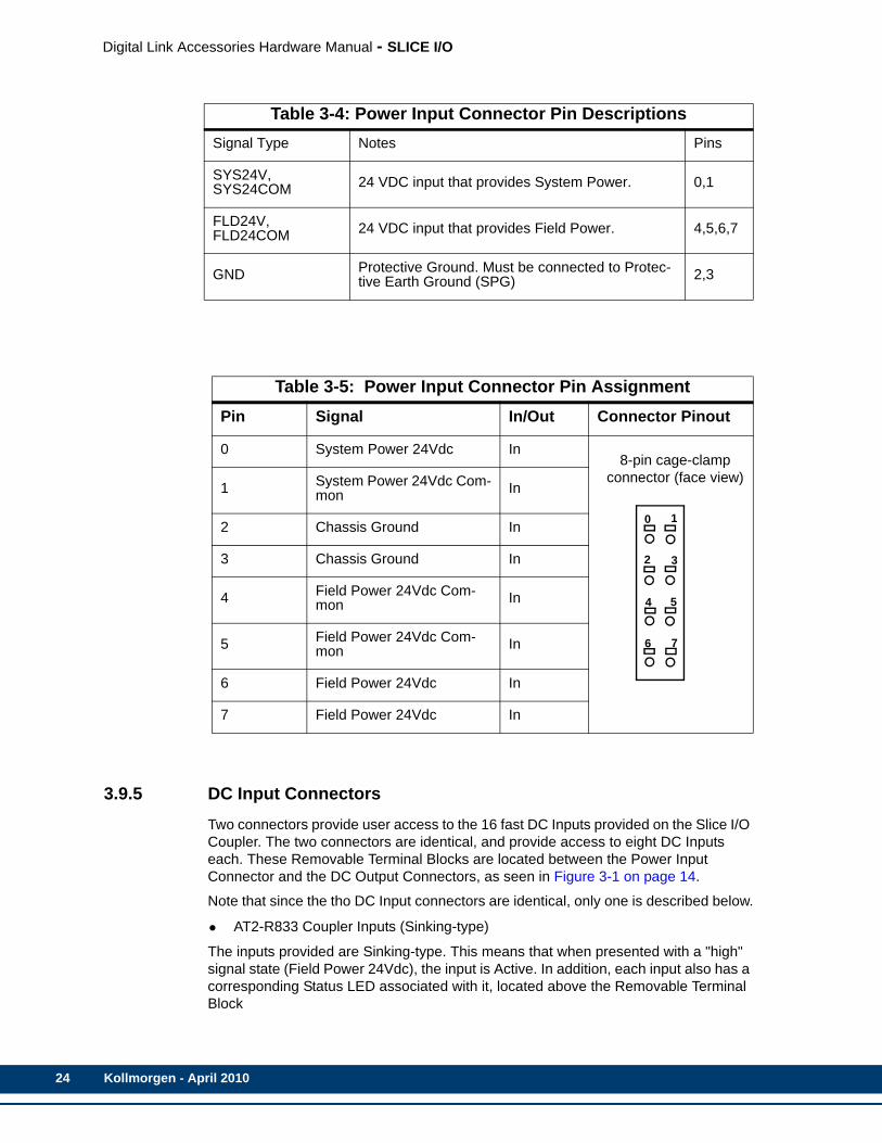
3.9.4 Power Input ConnectorThe 8-terminal Power Input Connector is used to bring User-provided System Power and Filed Power to the Slice I/O Coupler and attached Slice I/O Modules. This Removable Terminal Block is located at the left of the Coupler, as seen in Figure 3-1 on page 14.
• Pin descriptions are provided in Table 3-4
• Pin assignments are provided in Table 3-5
Table 3-3: Digital Link Port “IN” to “OUT” CablesPart Numbers:.3 M (1.0 ft): M.1302.8285 .6 M (2.0 ft): M.1302.8286 1 M (3.3 ft): M.1302.82872 M (6.6 ft): M.1302.8288 3 M (9.8 ft): M.1302.8289 5 M (16.4 ft): M.1302.83010 M (32.8 ft): M.1302.8301 15 M (49.2 ft): M.1302.8302 30 M (98.4 ft): M.1302.830Cable type: 28 AWG, shielded, twisted pair, 8 conductor.
8-Pin RJ-45 Plug (to Digital Link Port “OUT”, face view)
8-Pin RJ-45 Plug (to Digital Drive “IN”, face view)
Pin Signal Pin Signal Notes
1 Transmit Data + 1 Receive Data + Twisted
2 Transmit Data - 2 Receive Data - Pair
3 Receive Data + 3 Transmit Data + Twisted
6 Receive Data - 6 Transmit Data - Pair
4 None 4 None Twisted
5 None 5 None Pair
7 None 7 None Twisted
8 None 8 None Pair
Shell Drain Shell Drain
1
8
1
8
Kollmorgen - April 2010 23
24
Digital Link Accessories Hardware Manual - SLICE I/O
3.9.5 DC Input ConnectorsTwo connectors provide user access to the 16 fast DC Inputs provided on the Slice I/O Coupler. The two connectors are identical, and provide access to eight DC Inputs each. These Removable Terminal Blocks are located between the Power Input Connector and the DC Output Connectors, as seen in Figure 3-1 on page 14.
Note that since the tho DC Input connectors are identical, only one is described below.
• AT2-R833 Coupler Inputs (Sinking-type)
The inputs provided are Sinking-type. This means that when presented with a "high" signal state (Field Power 24Vdc), the input is Active. In addition, each input also has a corresponding Status LED associated with it, located above the Removable Terminal Block
Table 3-4: Power Input Connector Pin DescriptionsSignal Type Notes Pins
SYS24V, SYS24COM 24 VDC input that provides System Power. 0,1
FLD24V, FLD24COM 24 VDC input that provides Field Power. 4,5,6,7
GND Protective Ground. Must be connected to Protec-tive Earth Ground (SPG) 2,3
Table 3-5: Power Input Connector Pin AssignmentPin Signal In/Out Connector Pinout
0 System Power 24Vdc In8-pin cage-clamp
connector (face view)1 System Power 24Vdc Com-
mon In
2 Chassis Ground In
3 Chassis Ground In
4 Field Power 24Vdc Com-mon In
5 Field Power 24Vdc Com-mon In
6 Field Power 24Vdc In
7 Field Power 24Vdc In
0 1
2 3
4 5
6 7
Kollmorgen - April 2010

Digital Link Accessories Hardware Manual - SLICE I/O
For example, if a simple switch is being monitored by one of these inputs, connect one end of the switch to Field Power 24Vdc, and the other end of the switch to the desired input on the Removable Terminal Block. When the switch is open, the associated Status LED will be off, and the corresponding input bit, as read by the application program, will be low. When the switch is closed, the associated Status LED will be on, and the corresponding input bit, as read by the application program, will be high.
• AT2-R834 Coupler Inputs (Sourcing-type)
The inputs provided are Sourcing-type. This means that when presented with a "low" signal state (Field Power 24Vdc Common), the input is Active. In addition, each input also has a corresponding Status LED associated with it, located above the Removable Terminal Block
For example, if a simple switch is being monitored by one of these inputs, connect one end of the switch to Field Power 24Vdc Common, and the other end of the switch to the desired input on the Removable Terminal Block. When the switch is open, the associated Status LED will be off, and the corresponding input bit, as read by the application program, will be low. When the switch is closed, the associated Status LED will be on, and the corresponding input bit, as read by the application program, will be high.
• Pin descriptions are provided in Table 3-6
• Pin assignments are provided in Table 3-7
Table 3-6: DC Input Connector Pin Descriptions Signal Type Notes Pins
DCIN0 - DCIN7AT2-R833: Sinking-type 24Vdc (nominal) inputsAT2-R834: Sourcing-type 24Vdc (nominal) inputs
0 - 7
Kollmorgen - April 2010 25

26
Digital Link Accessories Hardware Manual - SLICE I/O
3.9.6 DC Output ConnectorsTwo connectors provide user access to the 16 fast DC Outputs provided on the Slice I/O Coupler. The two connectors are identical, and provide access to eight DC Outputs each. These Removable Terminal Blocks on the right side of the Coupler, as seen in Figure 3-1 on page 14.
Note that since the tho DC Output connectors are identical, only one is described below.
• AT2-R833 Coupler Outputs (Sourcing-type)
The Outputs provided are Sourcing-type. This means that when Active (written high by the application program), the Output is driven by Field Power 24Vdc. In addition, each Output also has a corresponding Status LED associated with it, located above the Removable Terminal Block
For example, if a simple light is being controlled by one of these outputs, connect one end of the light to Field Power 24Vdc Common, and the other end of the light to the desired output on the Removable Terminal Block. When the light is controlled off by the application program (written low), the associated Status LED will be off, and the light will be off. When the light is controlled on by the application program (written high), the associated Status LED will be on, and the light will be on.
• AT2-R834 Coupler Outputs (Sinking-type)
The Outputs provided are Sinking-type. This means that when Active (written high by the application program), the Output is driven by Field Power 24Vdc Common. In addition, each Output also has a corresponding Status LED associated with it, located above the Removable Terminal Block
For example, if a simple light is being controlled by one of these outputs, connect one end of the light to Field Power 24Vdc, and the other end of the light to the desired output on the Removable Terminal Block. When the light is controlled off by the
Table 3-7: DC Input Connector AssignmentPin Signal In/Out Connector Pinout
0 DC Input 0 In 8-pin cage-clamp connector (face view)
1 DC Input 1 In
2 DC Input 2 In
3 DC Input 3 In
4 DC Input 4 In
5 DC Input 5 In
6 DC Input 6 In
7 DC Input 7 In
0 1
2 3
4 5
6 7
Kollmorgen - April 2010
Digital Link Accessories Hardware Manual - SLICE I/O
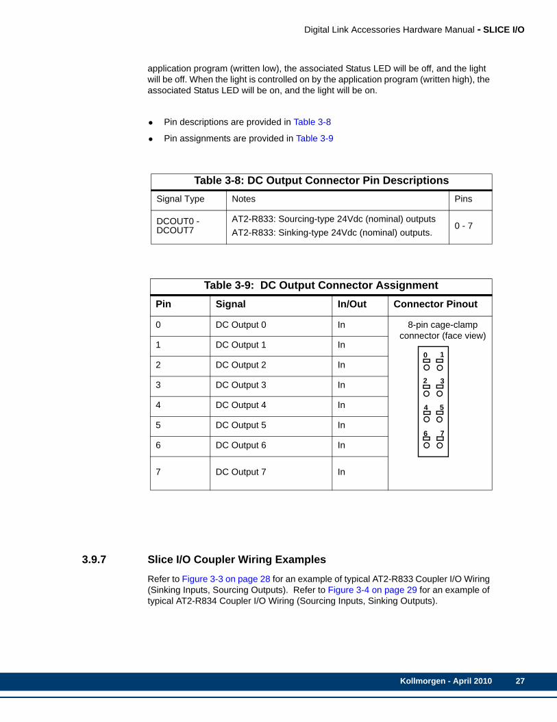
application program (written low), the associated Status LED will be off, and the light will be off. When the light is controlled on by the application program (written high), the associated Status LED will be on, and the light will be on.• Pin descriptions are provided in Table 3-8
• Pin assignments are provided in Table 3-9
3.9.7 Slice I/O Coupler Wiring ExamplesRefer to Figure 3-3 on page 28 for an example of typical AT2-R833 Coupler I/O Wiring (Sinking Inputs, Sourcing Outputs). Refer to Figure 3-4 on page 29 for an example of typical AT2-R834 Coupler I/O Wiring (Sourcing Inputs, Sinking Outputs).
Table 3-8: DC Output Connector Pin Descriptions Signal Type Notes Pins
DCOUT0 - DCOUT7
AT2-R833: Sourcing-type 24Vdc (nominal) outputsAT2-R833: Sinking-type 24Vdc (nominal) outputs.
0 - 7
Table 3-9: DC Output Connector AssignmentPin Signal In/Out Connector Pinout
0 DC Output 0 In 8-pin cage-clamp connector (face view)
1 DC Output 1 In
2 DC Output 2 In
3 DC Output 3 In
4 DC Output 4 In
5 DC Output 5 In
6 DC Output 6 In
7 DC Output 7 In
0 1
2 3
4 5
6 7
Kollmorgen - April 2010 27

28
Digital Link Accessories Hardware Manual - SLICE I/O
Figure 3-3: AT2-R833 Slice I/O Coupler Wiring Example
0 1
2 3
4 5
6 7
0 1
2 3
4 5
6 7
0 1
2 3
4 5
6 7
0 1
2 3
4 5
6 7
0 1
2 3
4 5
6 7
24VdcSystemPower
+ -
24VdcFieldPower
+ -
Single Point Ground
PlantGround
AdditionalPanels
Switches Lamp
Solenoid
Power Connector
Input Connector #1
Input Connector #2
Output Connector #1
Output Connector #2
Kollmorgen - April 2010

Digital Link Accessories Hardware Manual - SLICE I/O
Figure 3-4: AT2-R834 Slice I/O Coupler Wiring Example
0 1
2 3
4 5
6 7
0 1
2 3
4 5
6 7
0 1
2 3
4 5
6 7
0 1
2 3
4 5
6 7
0 1
2 3
4 5
6 7
24VdcSystemPower
+ -
24VdcFieldPower
+ -
Single Point Ground
PlantGround
AdditionalPanels
Switches Lamp
Solenoid
Power Connector
Input Connector #1
Input Connector #2
Output Connector #1
Output Connector #2
Kollmorgen - April 2010 29

30
Digital Link Accessories Hardware Manual - SLICE I/O
3.10 Slice I/O ModulesA wide variety of add-on Slice I/O Modules may be attached to the Slice I/O Coupler, including:
• DC and AC Input Modules
• DC, AC, and Relay Output Modules
• Analog Input Modules
• Analog Output Modules
• Power Supply and Power Distribution Modules
All Slice I/O Modules that will work with the Slice I/O Coupler are listed starting on Table 3-10 on page 31.
3.10.1 Slice I/O Limitations and PrecautionsWhen adding Slice I/O Modules, the following limitations and precautions must be observed:
• Each Slice I/O Module consumes a defined number of Input bytes and/or Output bytes (8 bits per byte). The Slice I/O Coupler supports a maximum of 16 Input bytes, and 16 Output bytes. The number of Input bytes and/or Output bytes that a particular module consumes is defined in the Module’s data sheet.
• There are limitations to the amount of System Power that can be provided by the Slice I/O Coupler. Refer to section 3.5.1 on page 15 for details.
• There are limitations to the amount of Field Power that can be provided through the Slice I/O Coupler. Refer to section 3.5.2 on page 15 for details.
• Many Slice I/O modules require Field Power other than 24Vdc, such as 5Vdc, 48Vdc, or 110Vac. When switching between Field Power voltages, it is absolutely necessary to install an Expansion Field Power Distributor (P/N ST-7241) between the Modules. Refer to the ST-7241 Data Sheet for additional information.
3.10.2 Slice I/O ModulesAll available Slice I/O Modules are listed in sections as follows:
• Digital Input Modules are listed in Table 3-10 on page 31.
• Digital Output Modules are listed in Table 3-11 on page 31.
• Analog Input Modules are listed in Table 3-12 on page 32.
• Analog Output Input Modules are listed in Table 3-13 on page 33.
• Power Modules are listed in Table 3-14 on page 33.
• Accessory Parts are listed in Table 3-15 on page 34.
WARNING
Failure to read and understand this section can result in damage to the entireSlice I/O System. This damage will not be covered under Kollmorgen’s war-ranty policy.
Kollmorgen - April 2010

Digital Link Accessories Hardware Manual - SLICE I/O
Data sheets for each individual Module can be found at:
http://www.crevis.co.kr/eng/htm/2_f_s_is.htm
Table 3-10: Digital Input Slice I/O ModulesPart Number Description
ST-1114 4 Point, Sink, 5Vdc
ST-1124 4 Point, Source, 5VDC
ST-1214 4 Point, Sink, 12V/24VDC
ST-1224 4 Point, Source, 12V/24VDC
ST-1218 8 Point, Sink, 12V/24VDC
ST-1228 8 Point, Source, 12V/24VDC
ST-121F
16 Point, Sink, 12V/24VDCNote: This module does not contain a Removable Terminal Block. Refer to Table 3-15 on page 34 for available mating connector.
ST-122F
16 Point, Source, 12V/24VDCNote: This module does not contain a Removable Terminal Block. Refer to Table 3-15 on page 34 for available mating connector.
ST-1314 4 Points, Sink, 48VDC
ST-1324 4 Points, Source, 48VDC
ST-1804 4 Points, 110VAC
ST-1904 4 Points, 220VAC
Table 3-11: Digital Output Slice I/O ModulesPart Number Description
ST-2114 4 Points, TTL Inverting, 5VDC/20mA
ST-2124 4 Points, TTL Non-Inverting, 5VDC/20mA
ST-2314 4 Points, Sink, 24VDC/0.5A
ST-2324 4 Points, Source, 24VDC/0.5A
ST-2414 4 Points, Sink, 24VDC/0.5A (with Diagnostic feedback)
Kollmorgen - April 2010 31

32
Digital Link Accessories Hardware Manual - SLICE I/O
ST-2424 4 Points, Source, 24VDC/0.5A (with Diagnostic feedback)
ST-2614 4 Points, Sink, 24VDC/2A
ST-2624 4 Points, Source, 24VDC/2A
ST-2514 4 Points, Sink, 24VDC/2A (with Diagnostic feedback)
ST-2524 4 Points, Source, 24VDC/2A (with Diagnostic feedback)
ST-2318 8 Points, Sink, 24VDC/0.5A
ST-2328 8 Points, Source, 24VDC/0.5A
ST-221F 16 Points, Sink, 20P Connector, 24VDC/0.5A (Does not have Removable Terminal Block)
ST-222F 16 Points, Source, 20P Connector, 24VDC/0.5A (Does not have Removable Terminal Block)
ST-2742 2 Points, Relay, 230VAC/2A, 24VDC/ 2A
ST-2744 4 Points, Relay, 230VAC/2A, 24VDC/ 2A
ST-2748 8 Points, Relay, 230VAC/2A, 24VDC/ 2A
ST-2852 2 Points, Triac, 120VAC/2A, 24VDC/2A
Table 3-12: Analog Input Slice I/O ModulesPart Number Description
ST-3114 4 Channels, 0~20mA, 12Bit
ST-3134 4 Channels, 0~20mA, 14Bit
ST-3118 8 Channels, 0~20mA, 12Bit
ST-3214 4 Channels, 4~20mA, 12Bit
ST-3234 4 Channels, 4~20mA, 14Bit
ST-3218 8 Channels, 4~20mA, 12Bit
ST-3624 4 Channels, 0~5VDC, 12Bit
ST-3644 4 Channels, 0~5VDC, 14Bit
ST-3424 4 Channels, 0~10VDC, 12Bit
ST-3444 4 Channels, 0~10VDC, 14Bit
Table 3-11: Digital Output Slice I/O Modules (Continued)
Kollmorgen - April 2010

Digital Link Accessories Hardware Manual - SLICE I/O
ST-3428 8 Channels, 0~10V, 12Bit
ST-3524 4 Channels, -10~+10VDC, 12Bit
ST-3544 4 Channels, -10~+10VDC, 14Bit
Table 3-13: Analog OutputPart Number Description
ST-4112 2 Channels, 0~20mA, 12Bit
ST-4114 4 Channels, 0~20mA, 12Bit
ST-4212 2 Channels, 4~20mA, 12Bit
ST-4214 4 Channels, 4~20mA, 12Bit
ST-4911 1 Channels, 0~1A, 12Bit
ST-4622 2 Channels, 0~5V, 12Bit
ST-4422 2 Channels, 0~10V, 1
ST-4424 4 Channels, 0~10V, 12Bit
ST-4522 2 Channels, -10~+10VDC, 12Bit
Table 3-14: Power ModulesPart Number Description
ST-7111 Expansion Power Supply (Input 24VDC/Output 1.0A/5VDC)
ST-7241 Expansion Field Power Distributor
ST-7008 Potential Distributor, for Shield
ST-7108 Potential Distributor, for 0VDC
ST-7118 Potential Distributor, for 24VDC
ST-7188 Potential Distributor, for 24VDC and 0VDC
Table 3-12: Analog Input Slice I/O Modules (Continued)
Kollmorgen - April 2010 33
34
Digital Link Accessories Hardware Manual - SLICE I/O
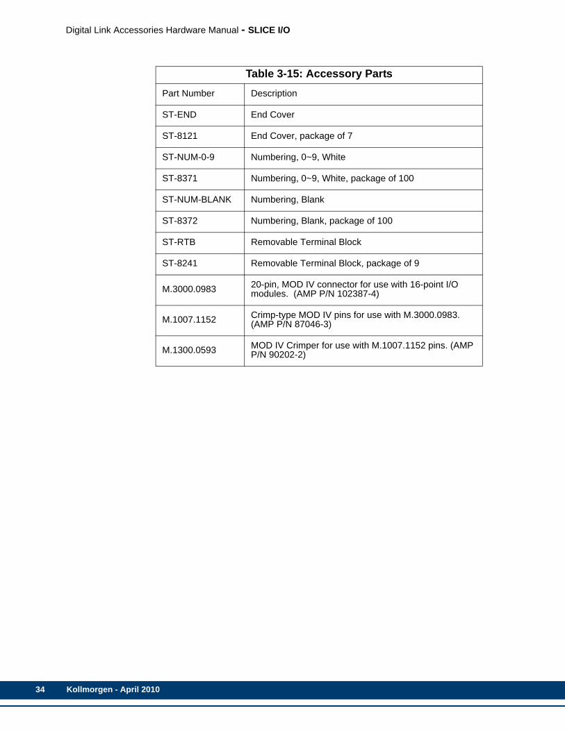
Table 3-15: Accessory PartsPart Number Description
ST-END End Cover
ST-8121 End Cover, package of 7
ST-NUM-0-9 Numbering, 0~9, White
ST-8371 Numbering, 0~9, White, package of 100
ST-NUM-BLANK Numbering, Blank
ST-8372 Numbering, Blank, package of 100
ST-RTB Removable Terminal Block
ST-8241 Removable Terminal Block, package of 9
M.3000.0983 20-pin, MOD IV connector for use with 16-point I/O modules. (AMP P/N 102387-4)
M.1007.1152 Crimp-type MOD IV pins for use with M.3000.0983. (AMP P/N 87046-3)
M.1300.0593 MOD IV Crimper for use with M.1007.1152 pins. (AMP P/N 90202-2)
Kollmorgen - April 2010

Digital Link Accessories Hardware Manual - SLICE I/O
3.11 Slice I/O Coupler Specifications
Part numberAT2-R833AT2-R834
Digital Link PortsIEEE 802.3/802.3u-100Base-TXCable type: Shielded, Straight Pinned, CAT5 or better (CAT5e, CAT6, etc.)Maximum cable length: 30 M (98.4 ft)
System Power Input 24Vdc (nominal), 20 VDC to 30 VDC, .5A Maximum
System Power Output 5Vdc (nominal), 1A Maximum (to connected Modules)
Field Power Input 24Vdc (nominal), 11Vdc to 28.8Vdc, 10A Maximum (depen-dent on current used for connected I/O)
Operating temperature range 5°C to 55°C (41°F to 131°F)
Storage temperature range -40°C to 85°C (-40°F to 185°F)
Humidity 5 to 90%, non-condensing
CE Marked (Pending)
Conforms to Directives 73/23/EEC, 89/336/EEC, 92/31/EEC, 93/68/EEC by conforming to the following standards:EN 50081-2:1993EMC Generic Industrial EmissionsEN 50082-2:1995EMC Generic Industrial ImmunityEN 61131-2:1994/A11:1996 Low voltage directive require-ments for programmable controllersOperates with emissions below EN55011/ CISPR 11Class A limitsImmune to:
•Electrostatic discharge (4K V contact mode, 8K V air discharge) per EN61000-4-2
•RF electromagnetic fields per EN61000-4-3, ENV 50141, and ENV50204
•Electrical fast transients per EN61000-4-4 •Magnetic fields per EN61000-4-8
Refer to the EMC Guidelines for more information.
UL and C/UL Listed UL File E235505
Physical size 3.27" wide x 3.90" high x 2.76" deep 83 mm x 99 mm x 70 mm
Vibration 10-57 Hz (.012in peak-to-peak)57 - 500 Hz (acceleration = 2 g)
Shock 10g
Kollmorgen - April 2010 35

36
Digital Link Accessories Hardware Manual - SLICE I/O
DC Inputs
Number of Inputs 16
Configuration AT2-R833: Sinking onlyAT2-R834: Sourcing only
Input voltage Nominal 24 VDC, maximum 28.8 VDC
Input current 4.5 mA at 24 VDC, typical
Guaranteed on voltage AT2-R833: 11 VDC (Minimum)AT2-R834: 5 VDC (Maximum)
Guaranteed off voltage AT2-R833: 5 VDC (Maximum)AT2-R834: 11 VDC (Minimum)
Turn on/off time 500 us
General DC Outputs
Number of outputs 16
ConfigurationAT2-R833: Sourcing onlyAT2-R834: Sinking only
Operating voltage Nominal 24 VDC (11 VDC Min, 28.8 VDC Max)
Protection of logic circuits Optical isolation between the logic and field side
Maximum current .5 A per output (8A total)
Switch characteristics Solid-state switches
Time delay on for resistive loads 300 µsec max
Time delay off for resistive loads 300 µsec max
Leakage current in off state 50 uA max
Voltage drop (Output ON) .3 VDC max
Over-current protection Yes
Short circuit protection Yes
Scan loss response Outputs turn off
Kollmorgen - April 2010

Digital Link Accessories Hardware Manual - DIGITAL LINK DRIVE INTERFACE UNIT
4 Digital Link Drive Interface UnitThis document contains Beta connection information on the Digital Link Drive Interface Unit (DL-DIU).
CE ENCLOSURE REQUIREMENTS
In order to meet the requirements of the CE Directives, the DL-DIU must bemounted within a grounded metal enclosure. Additional actions may also berequired, as described elsewhere within this manual.
Kollmorgen - November 2010 37

38
Digital Link Accesories Hardware Manual - DIGITAL LINK DRIVE INTERFACE UNIT
Figure 4-1:
DL-DIU
1
8
1
6
P
O
U
T
J
2
J
1
D
I
N
S
2
S
1
A
1
Kollmorgen - November 2010
Digital Link Accessories Hardware Manual - DIGITAL LINK DRIVE INTERFACE UNIT
4.1 DL-DIU Front Panel DetailsThis section explains in detail the various indicators and connectors located on the DL-DIU.
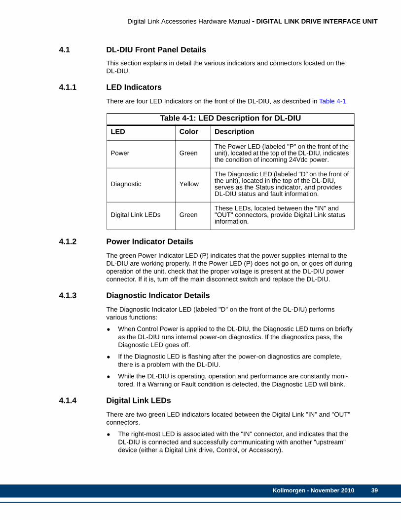
4.1.1 LED IndicatorsThere are four LED Indicators on the front of the DL-DIU, as described in Table 4-1.
4.1.2 Power Indicator DetailsThe green Power Indicator LED (P) indicates that the power supplies internal to the DL-DIU are working properly. If the Power LED (P) does not go on, or goes off during operation of the unit, check that the proper voltage is present at the DL-DIU power connector. If it is, turn off the main disconnect switch and replace the DL-DIU.
4.1.3 Diagnostic Indicator DetailsThe Diagnostic Indicator LED (labeled "D" on the front of the DL-DIU) performs various functions:
• When Control Power is applied to the DL-DIU, the Diagnostic LED turns on briefly as the DL-DIU runs internal power-on diagnostics. If the diagnostics pass, the Diagnostic LED goes off.
• If the Diagnostic LED is flashing after the power-on diagnostics are complete, there is a problem with the DL-DIU.
• While the DL-DIU is operating, operation and performance are constantly moni-tored. If a Warning or Fault condition is detected, the Diagnostic LED will blink.
4.1.4 Digital Link LEDsThere are two green LED indicators located between the Digital Link "IN" and "OUT" connectors.
• The right-most LED is associated with the "IN" connector, and indicates that the DL-DIU is connected and successfully communicating with another "upstream" device (either a Digital Link drive, Control, or Accessory).
Table 4-1: LED Description for DL-DIULED Color Description
Power GreenThe Power LED (labeled "P" on the front of the unit), located at the top of the DL-DIU, indicates the condition of incoming 24Vdc power.
Diagnostic YellowThe Diagnostic LED (labeled "D" on the front of the unit), located in the top of the DL-DIU, serves as the Status indicator, and provides DL-DIU status and fault information.
Digital Link LEDs GreenThese LEDs, located between the "IN" and "OUT" connectors, provide Digital Link status information.
Kollmorgen - November 2010 39

40
Digital Link Accesories Hardware Manual - DIGITAL LINK DRIVE INTERFACE UNIT
• The left-most LED is associated with the "OUT" connector, and indicates that the DL-DIU is connected and successfully communicating with another "downstream" device (either a Digital Link drive or Accessory).
4.1.5 Node Address Rotary SwitchesTwo rotary switches are used to set the DL-DIU address on the Digital Link. Rotate the switch to the desired address.
Addresses can be set to any number from 1 through 64. The top switch represents values of base ten. The bottom switch represents values of base 1.
As an example, rotating the top switch (S1) to a setting of 2 equals the value of 20 (2 x 10). Rotating the bottom switch (S2) to a setting of 5 equals the value of 5. The actual address setting is 25 (20 + 5).
Figure 4-2: Node Address Switches
S1 (10s)
S2 (1s)0
5
1
432
678
9
0
5
1
432
678
9
Kollmorgen - November 2010

Digital Link Accessories Hardware Manual - DIGITAL LINK DRIVE INTERFACE UNIT
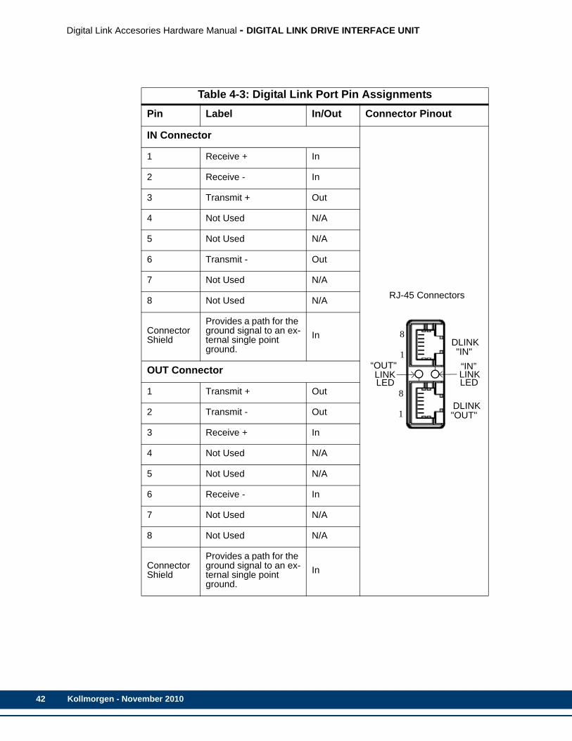
4.1.6 Digital Link PortsThe two 8-pin RJ-45 Digital Link Port connectors (labeled “IN” and “OUT” on the front of the DL-DIU) provide communications between the DL-DIU and:
• a Digital Link drive (MMC Smart Drive or S200-DLS Drive)
• a Digital Link Accessory (Slice I/O Coupler or another DL-DIU)
• an MMC-DSA Control (MMC-DSA2, -DSA4, -DSA8, -DSA16)
• a Digital Standalone MMC Control (MMC-D32, -D64)
Also provided are two green “Link” lights located between the RJ-45 connectors. The right light will be on if there is a Digital Link Device connected to the “IN” port, and the left light will be on if there is a Digital Link Device connected to the “OUT” port.
A “straight-through” shielded cable must be used when connecting to and from other devices. Connect the cable from the DL-DIU’s “OUT” port to the next Digital Link Device’s "IN” port, and from the previous Digital Link Device’s "OUT" port to the DL-DIU’s “IN” port. Refer to the Standalone MMC Hardware Manual for Standalone Digital Control information.
• Pin descriptions for are provided in Table 4-2
• Pin assignments are provided in Table 4-3
• The available Digital Link Port to Digital Drive cables are described in Table 4-4
Table 4-2: Digital Link Port Pin Description
Digital Link Connector (IN/OUT) Signals Pin
Function Notes“In”Connector
“Out” Connector
Receive Data+/- Receives data from connected devices. 1,2 3,6
Transmit Data +/- Transmits data to con-nected devices. 3,6 1,2
Protective Ground
Shield connection. Pro-vides a path for the ground signal to an ex-ternal single point ground.
Connector Shell Connector Shell
Kollmorgen - November 2010 41
42
Digital Link Accesories Hardware Manual - DIGITAL LINK DRIVE INTERFACE UNIT
Table 4-3: Digital Link Port Pin AssignmentsPin Label In/Out Connector Pinout
IN Connector
1 Receive + In
RJ-45 Connectors
2 Receive - In
3 Transmit + Out
4 Not Used N/A
5 Not Used N/A
6 Transmit - Out
7 Not Used N/A
8 Not Used N/A
Connector Shield
Provides a path for the ground signal to an ex-ternal single point ground.
In
OUT Connector
1 Transmit + Out
2 Transmit - Out
3 Receive + In
4 Not Used N/A
5 Not Used N/A
6 Receive - In
7 Not Used N/A
8 Not Used N/A
Connector Shield
Provides a path for the ground signal to an ex-ternal single point ground.
In
1
8
“OUT"LINK
“IN”LINKLEDLED
1
8DLINK "IN"
DLINK "OUT"
Kollmorgen - November 2010

Digital Link Accessories Hardware Manual - DIGITAL LINK DRIVE INTERFACE UNIT
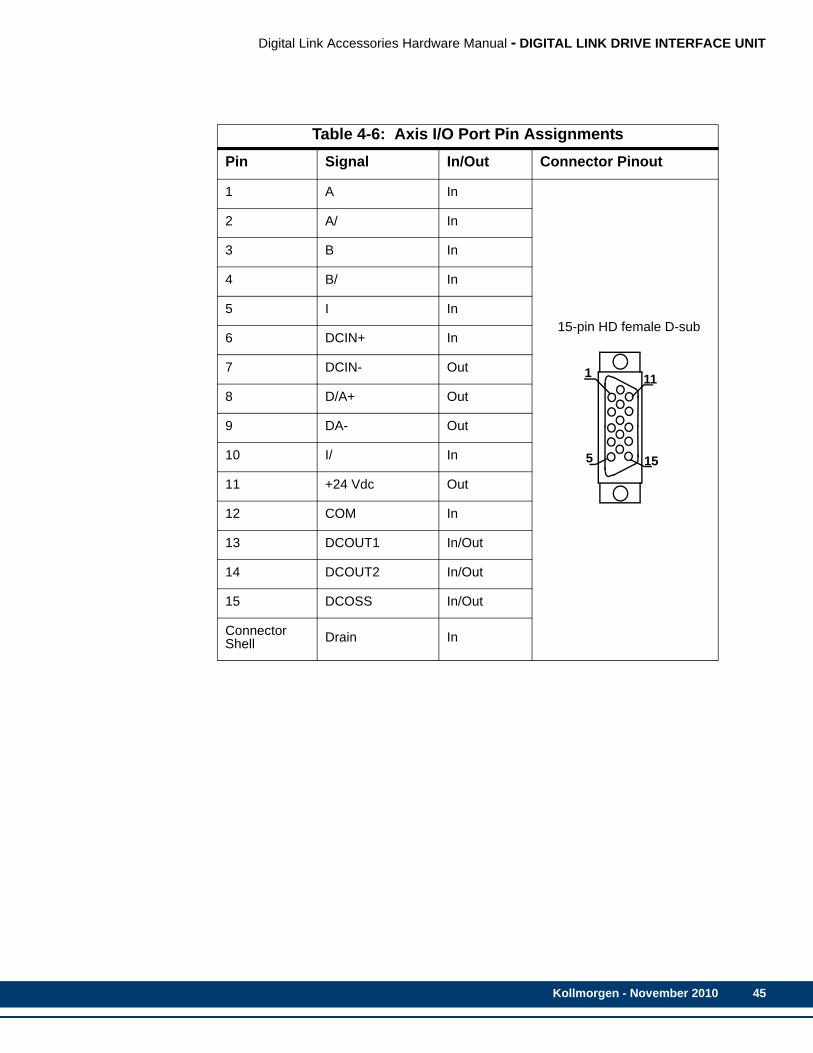
4.1.7 Axis I/O PortThe 15-pin HD female D-sub Axis I/O Port connector (labeled “A1” on the front of the DL-DIU) provides connection between the DL-DIU and an analog drive by providing the following:
• Two 24 Vdc outputs, described in detail in section 4.1.7.1 on page 47.
• One DC input, described in detail in section 4.1.7.2 on page 49.
• One 16-bit resolution analog output, described in detail in section 4.1.7.3 on page 50.
• One quadrature, incremental encoder input, described in detail in section 4.1.7.4 on page 51.
Additional information is provided in this section as follows:
Table 4-4: Digital Link Port “IN” to “OUT” CablesPart Numbers:.3 M (1.0 ft): M.1302.8285 .6 M (2.0 ft): M.1302.82861 M (3.3 ft): M.1302.8287 2 M (6.6 ft): M.1302.82883 M (9.8 ft): M.1302.8289 5 M (16.4 ft): M.1302.830010 M (32.8 ft): M.1302.8301 15 M (49.2 ft): M.1302.830230 M (98.4 ft): M.1302.8303Cable type: CAT-5 (or better), 28 AWG, shielded, twisted pair, 8 conductor.
8-Pin RJ-45 Plug (to Digital Link Port “OUT”,
face view)
8-Pin RJ-45 Plug (to Digital Port “IN”, face view)
Pin Signal Pin Signal Notes
1 Transmit Data + 1 Receive Data + Twisted
2 Transmit Data - 2 Receive Data - Pair
3 Receive Data + 3 Transmit Data + Twisted
6 Receive Data - 6 Transmit Data - Pair
4 None 4 None Twisted
5 None 5 None Pair
7 None 7 None Twisted
8 None 8 None Pair
Shell Drain Shell Drain
8
1 1
8
Kollmorgen - November 2010 43

44
Digital Link Accesories Hardware Manual - DIGITAL LINK DRIVE INTERFACE UNIT
• Pin descriptions provided in Table 4-5
• Pin assignments are provided in Table 4-6
• The available Flying Lead cable is described in Table 4-7.
• Available Breakout Boxes and Cables are described in Table 4-8.
• Breakout Box dimensions are shown in Figure 4-3
Table 4-5: Axis I/O Port Pin DescriptionsFunction Notes Pin
Encoder Input (A, A/, B, B/, I, I/)
Provides connections to an incremental en-coder having differential outputs. 1-5, 10
D/A Output (DA+, DA-) +/- 10V D/A output for controlling an analog drive having a differential input. 8, 9
DC Input (DCIN+, DCIN-)
Provides connection to an input device (sink or source). 6, 7
DC Outputs (DCOUT1, DCOUT2)
Provides connection to an output device (sink or source). 13, 14
DCOSS
Connect this pin to +24 Vdc to configure the outputs (DCOUT1 & DCOUT2) as sinking-type, and to +24 Vdc Common to configure the DC Outputs (DCOUT1 & DCOUT2) as sourcing-type.
15
24 Vdc out 24 Vdc output to be used to power connect-ed input and/or output devices. 11
COM 24 Vdc Common used to provide the 24 Vdc return path for sinking-type outputs. 12
Shield GroundProvides a path for shield current through the chassis to an external single point ground.
Shell
Kollmorgen - November 2010
Digital Link Accessories Hardware Manual - DIGITAL LINK DRIVE INTERFACE UNIT
Table 4-6: Axis I/O Port Pin AssignmentsPin Signal In/Out Connector Pinout
1 A In
15-pin HD female D-sub
2 A/ In
3 B In
4 B/ In
5 I In
6 DCIN+ In
7 DCIN- Out
8 D/A+ Out
9 DA- Out
10 I/ In
11 +24 Vdc Out
12 COM In
13 DCOUT1 In/Out
14 DCOUT2 In/Out
15 DCOSS In/Out
Connector Shell Drain In
5
1
15
11
Kollmorgen - November 2010 45
46
Digital Link Accesories Hardware Manual - DIGITAL LINK DRIVE INTERFACE UNIT
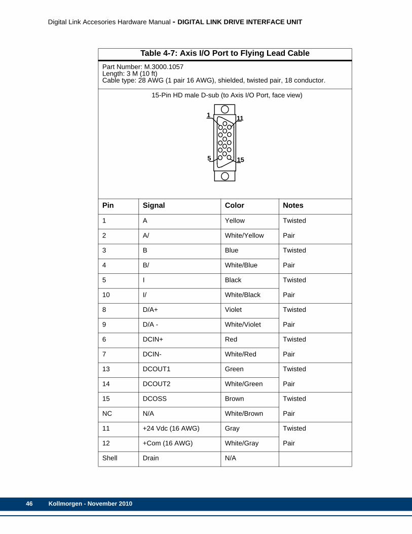
Table 4-7: Axis I/O Port to Flying Lead CablePart Number: M.3000.1057Length: 3 M (10 ft)Cable type: 28 AWG (1 pair 16 AWG), shielded, twisted pair, 18 conductor.
15-Pin HD male D-sub (to Axis I/O Port, face view)
Pin Signal Color Notes
1 A Yellow Twisted
2 A/ White/Yellow Pair
3 B Blue Twisted
4 B/ White/Blue Pair
5 I Black Twisted
10 I/ White/Black Pair
8 D/A+ Violet Twisted
9 D/A - White/Violet Pair
6 DCIN+ Red Twisted
7 DCIN- White/Red Pair
13 DCOUT1 Green Twisted
14 DCOUT2 White/Green Pair
15 DCOSS Brown Twisted
NC N/A White/Brown Pair
11 +24 Vdc (16 AWG) Gray Twisted
12 +Com (16 AWG) White/Gray Pair
Shell Drain N/A
5
1
15
11
Kollmorgen - November 2010

Digital Link Accessories Hardware Manual - DIGITAL LINK DRIVE INTERFACE UNIT
Figure 4-3: Axis I/O Port Breakout Box Dimensions
4.1.7.1 Axis I/O Port DC OutputsThe Axis I/O Port provides 2 sink or source 24 Vdc outputs. Each of the 2 outputs consists of an optically isolated solid state switch rated at 100 ma. It turns on or off according to the logic state sent to it by the user program. When the switch turns on, current flows through the switch. When the switch turns off, current flow stops. When the DCOSS pin is tied to the +24V, the outputs will be in a source configuration as
Table 4-8: Axis I/O Port Connection AccessoriesDescription Length Part Number
Axis I/O Port Breakout Boarda
a. The Breakout Board is mounted directly onto the Axis I/O Port Connector, and provides screw terminal wire termination to each of the Axis I/O Connector’s sig-nal pins as well as to the shell of the connector.
N/A M.1302.6970
Axis I/O Port Breakout Boxb
b. The Breakout Box (see Figure 4-3 on page 47) is DIN-rail mounted, and pro-vides screw terminal wire termination. It can be attached to the A1 port on the DL-DIU. The pinouts on the terminal strip interface provide a one-to-one transfer of the signals from the connector to the respective pin(s) on the terminal block. The ground pin on the terminal strip provides a connection to the metal D-shell.
N/A M.1016.2529
Axis I/O Port Breakout Box Cable .3 M (1 ft) M.3000.1058
Axis I/O Port Breakout Box Cable .6 M (2 ft) M.3000.1059
Axis I/O Port Breakout Box Cable .9 M (3 ft) M.3000.1060
1.750”
2.250”
3.000”
1
9
2.250”
8
15
Kollmorgen - November 2010 47

48
Digital Link Accesories Hardware Manual - DIGITAL LINK DRIVE INTERFACE UNIT
shown in Figure 4-4. When the DCOSS pin is tied to COMMON, the outputs will be in a sink configuration as shown in Figure 4-5.
These outputs are intended to interface with the drive enable and drive reset inputs.
For safety reasons, all outputs turn off (no current flow) when a scan loss condition occurs.
For more information on DC output operation, refer to Section 6.3 on page 74 of Appendix A.
Figure 4-4: Axis I/O DC Output Source Configuration
DC OUT 1
DCOSS
DC OUT 2
+24VCOM
13
15
14
11
12
DriveEnable
DriveReset
Sourcing Outputs Sourcing Inputs
DL-DIU Axis I/O Connector Drive
Kollmorgen - November 2010

Digital Link Accessories Hardware Manual - DIGITAL LINK DRIVE INTERFACE UNIT
Figure 4-5: Axis I/O DC Output Sink Configuration
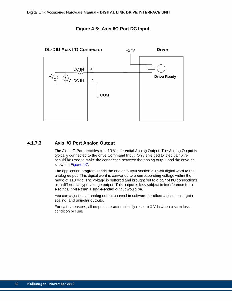
4.1.7.2 Axis I/O Port DC InputThe Axis I/O Port provides one 24 Vdc input. This input consists of an optically isolated solid state switch that can be wired in either a sourcing or sinking configuration. The input is turned on or off by the connected external device. One of the input pins should be connected to either +24 Vdc or COM. The remaining input pin should be tied to the input device. Refer to Figure 4-6.
This input is intended to interface with the drive ready output.
For more information on DC input operation, refer to Section 6.2 on page 73 of Appendix A.
DC OUT 1
DCOSS
DC OUT 2
+24V
COM
13
15
14
11
12
DriveEnable
DriveReset
Sinking Outputs Sinking Inputs
+24V
+24V
DL-DIU Axis I/O Connector Drive
Kollmorgen - November 2010 49
50
Digital Link Accesories Hardware Manual - DIGITAL LINK DRIVE INTERFACE UNIT
Figure 4-6: Axis I/O Port DC Input
4.1.7.3 Axis I/O Port Analog OutputThe Axis I/O Port provides a +/-10 V differential Analog Output. The Analog Output is typically connected to the drive Command Input. Only shielded twisted pair wire should be used to make the connection between the analog output and the drive as shown in Figure 4-7.
The application program sends the analog output section a 16-bit digital word to the analog output. This digital word is converted to a corresponding voltage within the range of ±10 Vdc. The voltage is buffered and brought out to a pair of I/O connections as a differential type voltage output. This output is less subject to interference from electrical noise than a single-ended output would be.
You can adjust each analog output channel in software for offset adjustments, gain scaling, and unipolar outputs.
For safety reasons, all outputs are automatically reset to 0 Vdc when a scan loss condition occurs.
DL-DIU Axis I/O Connector Drive
Drive Ready
DC IN+
DC IN -
6
7
COM
+24V
Kollmorgen - November 2010
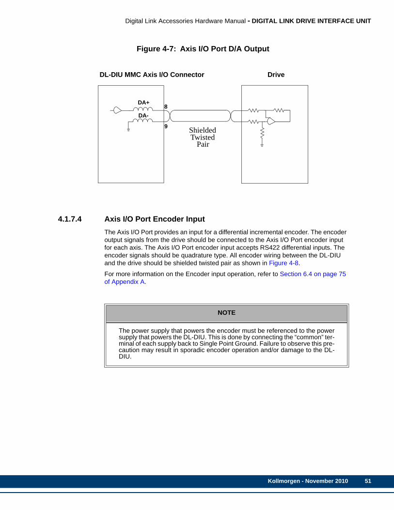
Digital Link Accessories Hardware Manual - DIGITAL LINK DRIVE INTERFACE UNIT
Figure 4-7: Axis I/O Port D/A Output
4.1.7.4 Axis I/O Port Encoder InputThe Axis I/O Port provides an input for a differential incremental encoder. The encoder output signals from the drive should be connected to the Axis I/O Port encoder input for each axis. The Axis I/O Port encoder input accepts RS422 differential inputs. The encoder signals should be quadrature type. All encoder wiring between the DL-DIU and the drive should be shielded twisted pair as shown in Figure 4-8.
For more information on the Encoder input operation, refer to Section 6.4 on page 75 of Appendix A.
NOTE
The power supply that powers the encoder must be referenced to the powersupply that powers the DL-DIU. This is done by connecting the “common” ter-minal of each supply back to Single Point Ground. Failure to observe this pre-caution may result in sporadic encoder operation and/or damage to the DL-DIU.
DA+
DA-8
9
DL-DIU MMC Axis I/O Connector Drive
ShieldedTwisted
Pair
Kollmorgen - November 2010 51
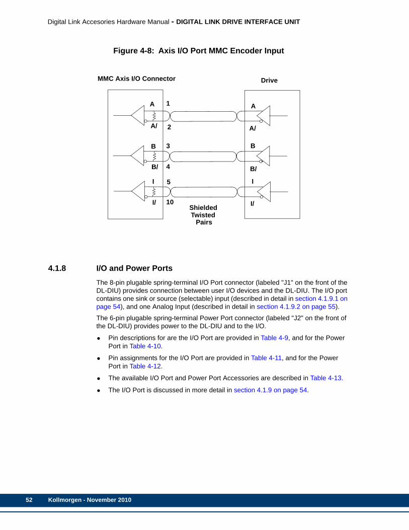
52
Digital Link Accesories Hardware Manual - DIGITAL LINK DRIVE INTERFACE UNIT
Figure 4-8: Axis I/O Port MMC Encoder Input
4.1.8 I/O and Power PortsThe 8-pin plugable spring-terminal I/O Port connector (labeled "J1" on the front of the DL-DIU) provides connection between user I/O devices and the DL-DIU. The I/O port contains one sink or source (selectable) input (described in detail in section 4.1.9.1 on page 54), and one Analog Input (described in detail in section 4.1.9.2 on page 55).
The 6-pin plugable spring-terminal Power Port connector (labeled "J2" on the front of the DL-DIU) provides power to the DL-DIU and to the I/O.
• Pin descriptions for are the I/O Port are provided in Table 4-9, and for the Power Port in Table 4-10.
• Pin assignments for the I/O Port are provided in Table 4-11, and for the Power Port in Table 4-12.
• The available I/O Port and Power Port Accessories are described in Table 4-13.
• The I/O Port is discussed in more detail in section 4.1.9 on page 54.
A
A/
I
B
I/
B/
A
A/
B
B/
I
I/
MMC Axis I/O Connector Drive
1
2
3
4
5
10ShieldedTwisted
Pairs
Kollmorgen - November 2010

Digital Link Accessories Hardware Manual - DIGITAL LINK DRIVE INTERFACE UNIT
Table 4-9: I/O Port (J1) Pin DescriptionsFunction Notes Pin
DC Input 1 24 Vdc (nominal) sourcing/sinking Inputs 5
Analog Input +/- 10V, 1mv resolution 6,7
Reserved for future use. Do not connect These pins will provide future functionality. 1,2,3,4,8
Table 4-10: I/O Port Pin AssignmentsPin Signal In/Out Connector Pinout
1 Do Not Connect N/A8-Pin plugable Screw Terminal Connector2 Do Not Connect N/A
3 Do Not Connect N/A
4 Do Not Connect N/A
5 DC Input 1 In
6 Analog Input + In
7 Analog Input - In
8 Do Not Connect N/A
1
8
"J1"I/O
Kollmorgen - November 2010 53

54
Digital Link Accesories Hardware Manual - DIGITAL LINK DRIVE INTERFACE UNIT
4.1.9 I/O Port DetailsThere is one DC Input and one analog Input available for interfacing to various devices. This section explains these Inputs in detail.
4.1.9.1 I/O Port InputThe I/O Port provides one sink/source 24 Vdc input.
Table 4-11: Power Port Pin DescriptionsFunction Notes Pin
I/O 24V Power 24Vdc (nominal) to power the DL-DIU and the I/O 4
I/O 24V Common I/O 24V common 5
DC Input 1 Sink/source
This pin determines whether I/O input 1 is sourcing (this pin connected to 24 Vdc Com-mon) or sinking (this pin connected to 24 Vdc)
1
Chassis Ground This pin should be connected to Chassis Ground 6
Table 4-12: Power Port Pin AssignmentsPin Signal In/Out Connector Pinout
1 Input 1 Sink/Source In 6-Pin plugable Screw Terminal Connector
2 Do not Connect N/A
3 Do Not Connect N/A
4 I/O 24 Vdc N/A
5 I/O 24 Vdc Common In
6 Chassis Ground In
Table 4-13: I/O and Power Port AccessoriesDescription Part Number
6-pin spring-contact pluggable mating connector for the I/O Power Port (J2) M.1302.7662
8-pin spring-contact pluggable mating for connector for the I/O Port (J1) M.1302.7627
1
6
"J6"
POWERI/O
Kollmorgen - November 2010

Digital Link Accessories Hardware Manual - DIGITAL LINK DRIVE INTERFACE UNIT
To configure the Input as Sinking, the Sink/Source select pin (pin 1), must be connected to 24 Vdc. When configured as Sinking, one side of the input device is connected to the Input pin on the I/O Port connector, and the other side of the input device must be connected to 24 Vdc Common.
To configure an Input as Sourcing, the Sink/Source select pin (pin 1), must be connected to 24 Vdc Common. When configured as Sourcing, one side of the input device is connected to the Input pin on the I/O Port connector, and the other side of the input device must be connected to 24 Vdc.
4.1.9.2 Analog InputThe I/O Port provides one differential analog input channel. The input range is ±10 VDC (nominal), with 1mv resolution. The analog input voltage is sampled every 125 µsec and the 16-bit result is stored in an on-board register. This register can be read at any time by the application.
The analog input signal passes through a common mode and differential mode filter prior to being applied to the A/D converter. These filters improve the noise immunity of the converter.
4.1.9.3 I/O Port Wiring ExampleAn example of wiring the I/O is shown in See Figure 4-9 on page 56.
• The Sink/Source select pin for Input 1 on the I/O Power Port connector is con-nected to 24 Vdc, making Inputs 1 Sinking. In this configuration, one side of the input device is connected to the Input pin on the I/O Port connector, and the other side of the input device is connected to 24 Vdc Common.
Kollmorgen - November 2010 55

56
Digital Link Accesories Hardware Manual - DIGITAL LINK DRIVE INTERFACE UNIT
Figure 4-9: Connecting Devices to the I/O Port
To
I/O Port
24 Vdc Power Supply+ _
SPG
Input SS
2
6
3
6
7
4
3
2
1
5
24VDCIN
5
4
24VDC COM
DCIN1
8
1
CHASSIS
"J1"I/O
"J2"POWER
SINKING
N/C
N/C
N/C
N/C
N/C
N/C
N/C
N/C
N/C
TwistedPair
Shielded+/- 10VdcANIN-
ANIN+
Kollmorgen - November 2010

Digital Link Accessories Hardware Manual - DIGITAL LINK DRIVE INTERFACE UNIT
4.2 Specifications
Table 4-14: DL-DIU Specifications
Function •Provides Digital Link control of an Analog Drive•Provides a +/-10Vdc Analog Input
Part Number M.3000.0832
Input voltage 20 VDC to 30 VDC
Input power 100ma typical
Operating temperature range 5°C to 55°C (41°F to 131°F)
Storage temperature range -40°C to 85°C (-40°F to 185°F)
Humidity 5 to 95%, non-condensing
CE Marked(Pending)
Conforms to Directives 73/23/EEC, 89/336/EEC, 92/31/EEC, 93/68/EEC by conforming to the following standards:EN 50081-2:1993EMC Generic Industrial EmissionsEN 50082-2:1995EMC Generic Industrial ImmunityEN 61131-2:1994/A11:1996 Low voltage directive require-ments for programmable controllersOperates with emissions below EN55011/ CISPR 11Class A limitsImmune to:
•Electrostatic discharge (4K V contact mode, 8K V air discharge) per EN61000-4-2
•RF electromagnetic fields per EN61000-4-3, ENV 50141, and ENV50204
•Electrical fast transients per EN61000-4-4 •Magnetic fields per EN61000-4-8
Refer to the EMC Guidelines for more information.
UL and C/UL Listed E126417
Physical size 1.125" wide x 6.0" high x 4.0" deep 28.57 mm x 152.4 mm x 101.6 mm
Vibration (per IEC 68-2-6) 10-57 Hz (constant amplitude = .15 mm)57 - 2000 Hz (acceleration = 2 g)
Shock (per IEC 68-2-27) Four shocks per axis (15g/11 msec)
Kollmorgen - November 2010 57

58
Digital Link Accesories Hardware Manual - DIGITAL LINK DRIVE INTERFACE UNIT
Axis Port Analog Output
Output channels 1
Resolution 16 bits
Output voltage range ±10 VDC
Maximum output current (1K Ω load) ±10 mA
Power on output voltage 0 V ±100 mV
Scan loss output voltage 0V ±100 mV
Accuracy ±0.375% of FSR Drift ± 50ppm/°C
Update rate 125 µsec
Axis Port Encoder Input
Input channels 1
Input receiver Maxim 3098 A quad B differential RS422 receiver
Recommended Encoder Drivers 7272, 75183, 8830, 75114, 9614, 26LS31 (or equivalent)
Encoder signals Differential quadrature
Input threshold ±750 mV
Input termination 150 ohm, provided on board
Maximum input voltage 5 V
Maximum input signal frequency 720 Khz (2.88 M feedback unit count rate)
I/O Port Analog Input
Input channels 1
Resolution 1mv
Input voltage range ±10.24 V
Accuracy ±1% of FSR
Sample rate 125 µsec
Common mode filter 3 dB @ 122 Khz
Differential mode filter 3 dB @ 1826 Hz
Kollmorgen - November 2010

Digital Link Accessories Hardware Manual - DIGITAL LINK DRIVE INTERFACE UNIT
Axis and I/O Port Inputs
ConfigurationAxis I/O Ports Inputs: Sink or Source (1)I/O Port Input: Sink or Source (1)
Operates with IEC Type 1 inputs (per IEC 1131-2).
Input voltage Nominal 24 VDC, maximum 30 VDC
Guaranteed on voltage 15 VDC
Guaranteed off voltage 5 VDC
Turn on/off time 1 ms
Fast Input (Input 1, located on J1, pin 5) 50 μsec turn-on, 400 μsec turn-off
Axis Port DC Outputs
Number of outputs 2
Configuration The set of axis outputs can be configured as sourcing or sink-ing.
Maximum current 100 mA per output
Voltage range 24 VDC nominal, 5 to 30 VDC range
Scan loss response Outputs turn off
Kollmorgen - November 2010 59

60
Digital Link Accesories Hardware Manual - DIGITAL LINK DRIVE INTERFACE UNIT
Kollmorgen - November 2010

Digital Link Accessories Hardware Manual - CE AND EMC GUIDELINES
5 CE and EMC Guidelines
5.1 Background on EMC (Electromagnetic Compatibility) ComplianceIn order to market products in the European Union after January 1, 1996, an electromagnetic compatibility directive (EU Directive 89/336/ECC) must be met. All products must be designed and manufactured in such a way that:
• Electromagnetic disturbances generated by the products do not cause interfer-ence to other systems.
• The performance of the product is not affected by electromagnetic disturbances within the environment in which the product is intended to operate.
The directive refers to relevant harmonized European EMC standards against which product conformity can be assessed, although other methods of assessment, notably the preparation of a Technical File, are permissible. The equipment manufacturer or the manufacturer’s agent in the Community must make a Declaration of Conformity and can place the CE mark on the product. Failure to conform with the requirements of the directive can result in a total ban on sales throughout the Single Market and legal action could be taken against the signatory of a false declaration of conformity.
5.2 Background on Low Voltage ComplianceIn order to market products in the European Union after January 1, 1997, the low voltage directive (EU Directive 73/23/EEC) must be met.
The intention of the directive is to assure user safety under normal operating and fault conditions. The directive includes the use of certain warning labels and user instructions. It establishes limits to prevent electrical shock hazard, overheating and fire.
5.3 RFI Emission and ImmunityThe EMC product characteristics are classified by the emission and immunity performance.
Emissions not only include radiated noise from the product enclosure and cabling, but also that which is conducted away from the product along the cables connected to it. This may be subsequently radiated from the cable or conducted directly into another product which shares this cable e.g. the main AC supply.
Immunity is how susceptible a product is (e.g. to the radiated and conducted emissions from the product mounted next to it). To ensure compatibility, the immunity of a product must always exceed the expected emissions in the environment in which it operates as is shown in the diagram below. This is to ensure a margin of safety.
NOTE
The CE mark on PiC products assures compliance with both the EMC andlow voltage European directives. Prior to this CE mark, EMC on the productlabel only assured compliance with the EMC directives.
Kollmorgen - April 2010 61
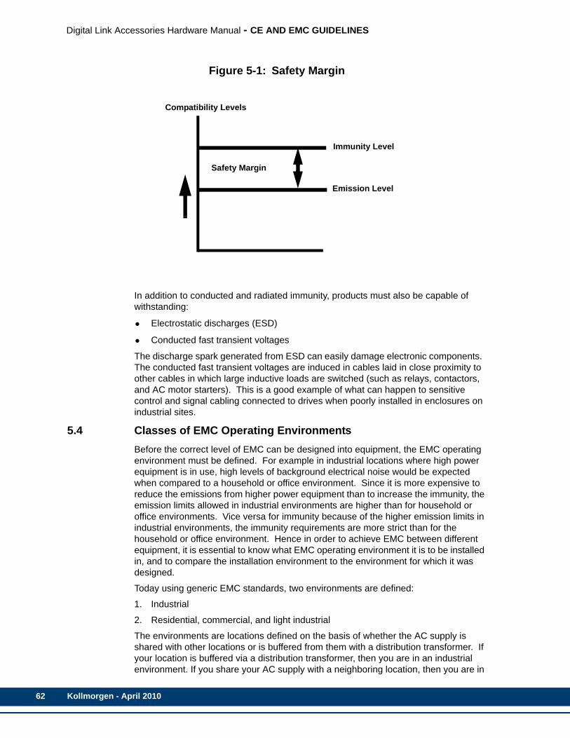
62
Digital Link Accessories Hardware Manual - CE AND EMC GUIDELINES
Figure 5-1: Safety Margin
In addition to conducted and radiated immunity, products must also be capable of withstanding:
• Electrostatic discharges (ESD)
• Conducted fast transient voltages
The discharge spark generated from ESD can easily damage electronic components. The conducted fast transient voltages are induced in cables laid in close proximity to other cables in which large inductive loads are switched (such as relays, contactors, and AC motor starters). This is a good example of what can happen to sensitive control and signal cabling connected to drives when poorly installed in enclosures on industrial sites.
5.4 Classes of EMC Operating EnvironmentsBefore the correct level of EMC can be designed into equipment, the EMC operating environment must be defined. For example in industrial locations where high power equipment is in use, high levels of background electrical noise would be expected when compared to a household or office environment. Since it is more expensive to reduce the emissions from higher power equipment than to increase the immunity, the emission limits allowed in industrial environments are higher than for household or office environments. Vice versa for immunity because of the higher emission limits in industrial environments, the immunity requirements are more strict than for the household or office environment. Hence in order to achieve EMC between different equipment, it is essential to know what EMC operating environment it is to be installed in, and to compare the installation environment to the environment for which it was designed.
Today using generic EMC standards, two environments are defined:
1. Industrial
2. Residential, commercial, and light industrial
The environments are locations defined on the basis of whether the AC supply is shared with other locations or is buffered from them with a distribution transformer. If your location is buffered via a distribution transformer, then you are in an industrial environment. If you share your AC supply with a neighboring location, then you are in
Compatibility Levels
Safety Margin
Immunity Level
Emission Level
Kollmorgen - April 2010

Digital Link Accessories Hardware Manual - CE AND EMC GUIDELINES
a residential, commercial, or light industrial environment. For example, an industrial unit which shares its AC supply with a neighboring unit is defined as a residential, commercial, and light industrial location. If it is supplied from its own distribution transformer, then it is an industrial location.
5.5 Conformance with the EMC DirectiveKollmorgen will be complying to the Directive by self-certification to the following generic EMC standards:
• EN50081-2 for industrial emissions using EN55011 (based upon CISPR 11A)
• EN50082-2 for industrial immunity using:
• IEC 61000-4-2 (ESD- 4KV contact mode, 8 KV air discharge)
• IEC 61000-4-3 (Radiated susceptibility)
• IEC 61000-4-4 (Electrical fast transient)
• IEC 6100-4-8 (Magnetic fields)
A statement of compliance will be made with the letters “EMC” or “CE” on the product, but will be valid only if the product is installed properly.
5.6 Conformance With the Low Voltage DirectiveKollmorgen will comply with the Directive by self certification to the following standard:
• EN 61131-2:1994/A11:1996 Low Voltage Requirements for Programmable Con-trollers
A statement of compliance will be made with the letters “CE” on the product but will be valid only if the equipment is properly installed.
5.7 Changes to the PiC ProductsKollmorgen PiC products had originally been designed with a high level of noise immunity and tested according to standards such as NEMA showering arc and the original version of IEC 801-2. However, the EU directive for immunity requires testing to standards that have more variables and are more repeatable. The directive also requires control of emissions, something that is not regulated in U. S. industrial environments.
As a result, changes have been made to the hardware modules within the PiC product line. The changes have included the addition of filtering, re-routing of foils and/or the addition of ground planes to printed circuit boards, use of some conductive enclosures, provision for shielded wires (see Note below) for peer-to-peer communication, and internal connection of SPG to field side connectors.
5.7.1 Changes Affecting the UserMany of the changes Kollmorgen has implemented are transparent to the user. However, there are some changes affecting user installation.
Kollmorgen continues to recommend separation of low level signals (encoder, analog, communications, fast DC inputs) from high voltage or high current lines from any of
NOTE
A recommended shielded wire is Belden, 24 AWG (7X32), 9729
Kollmorgen - April 2010 63

64
Digital Link Accessories Hardware Manual - CE AND EMC GUIDELINES
the above. More specifically, maintain at least one inch of separation around encoder signals and around communication signals.
It is no longer necessary to connect a wire from a module to SPG. This user-installed wire had been a source of emissions and thus the connection should not be made. Analog modules typically had this requirement in the past.
To prevent excessive conducted emissions from a DC power source (typically 24V) used for digital I/O, a 1000 picofarad capacitor should be used. Connect the capacitor from the +24V DC to COMMON at the distribution terminals. The same applies to any other external DC power source used with the PiC product.
The figure on the left below illustrates the connection method before EMC compliant products were available. The figure on the right illustrates the recommended connections when using EMC compliant products. On the right, note that the SPG connection has been eliminated and that a capacitor is connected to the 24V DC supply.
Figure 5-2: Connections for EMC Compliance
There is now a provision for shield termination to the CPU modules for peer-to-peer communication. Shielded cable must be used to reduce emissions.
Inside a control cabinet, the practice of connecting the shields of shielded cables at the modules should be continued. For an example of a shielded cable entering/leaving the cabinet see Figure 5-3 on page 65.
MMCSYSTEM
COMMUNICATIONS
ANALOG
AC INPUT/OUTPUT
DC INPUT/OUTPUT
SINGLE-POINT GROUND
AC INPUTPOWER
GND
DC POWERSUPPLY
to AC I/O to DC I/O+
ENCODER, MMCSYSTEM
COMMUNICATIONS
ANALOG
AC INPUT/OUTPUT
DC INPUT/OUTPUT
SINGLE-POINT GROUND
AC INPUTPOWER
GND
DC POWERSUPPLY
to AC I/O to DC I/O+
ENCODER,
capacitor
Connections before RecommendedEMC Compliant Products EMC Compliant Connections
Kollmorgen - April 2010

Digital Link Accessories Hardware Manual - CE AND EMC GUIDELINES
Figure 5-3: Connecting Shielded Cable
The two different methods of terminating shields are used to accommodate two different immunity requirements. Immunity required inside an enclosure is considered lower because cables are typically less than 3 meters in length and/or can be separated from each other and from noise sources.
Immunity required external to an enclosure is considered higher because the user may have less control over the noise environment. Low level signal cables that can be external to an enclosure and AC/DC digital I/O cables have been tested at a 2 KV level for electrical fast transients (EFTs). Low level signals that can be less than 3 meters in length or can be separated from noise sources are tested at a 1 KV level.
Under the stated conditions, there will be no disturbance of digital I/O, encoder, or stepper operation. For analog signals, there may be momentary disturbances but there will be self-recovery when the noise subsides.
In order to meet the EU directive requirement for emissions and immunity, fiber optics must be used for I/O expansion.
Although the control will pass the electrical fast transient test on incoming power lines, users may still want to use a power line conditioner.
As a general precaution, do not operate transmitters, arc welding equipment, or other high noise radiators within one meter of a PiC enclosure that has the door open. Continue to equip inductive devices, if they are in series with a mechanical contact or switch, with arc suppression circuits. These devices include contactors, solenoids and motors. Shield all cables that carry heavy current near the system, using continuous foil wrap or conduit grounded at both ends. Such cables include power leads for high-frequency welders and for pulse-width-modulated motor drives.
Worst case tests with analog I/O modules have caused momentary disturbances no greater than .5V in a +10V to -10V range and .5 mA in a 4 to 20 mA range. Worst case tests with an RTD module have caused momentary disturbances no greater that + or -
NOTE
Shields for signal wires are grounded at only one end, to provide immunity tooutside noise sources. However, the shields for “noise sources” are ground-ed at both ends, to reduce emissions and “contain” the noise.
MMCModule
ExternalDevice
CabinetEnclosure
Kollmorgen - April 2010 65

66
Digital Link Accessories Hardware Manual - CE AND EMC GUIDELINES
4°C in a range of -200° to 266°C. Worst case tests with a JK thermocouple module have caused momentary disturbances no greater than + or - 1 mV over a 100 to 1.
5.8 Using CE/EMC and Non-CE/EMC Modules
There are several issues that must be considered when using CE/EMC compliant and Non-CE/EMC compliant Modules. This document addresses these issues.
Module Identification - To determine whether a module is CE/EMC or Non-CE/EMC, look at the gray Unit Tag located on the side of the plastic module case. CE/EMC modules will have “CE” or “EMC” printed near the “MAX. AMBIENT TEMP.” specification. Non-CE/EMC will not have “CE” or “EMC” printed in this location.
Grounding - Due to differences in shielding requirements, it is extremely important to follow proper shielding guidelines for a given module. Failure to do so may result in intermittent operation in noisy environments.
For modules that have an SPG terminal and/or one or more SHIELD terminal, perform the following:
• For CE/EMC modules, do not connect the SPG terminal or SHIELD terminals to the system’s Single Point Ground
• For Non-CE/EMC modules, connect the SPG terminal, or a SHIELD terminal, to the system’s Single Point Ground
CE/EMC CSM and RSM Modules - Using a CE/EMC CSM, RSM, or CSM/CPU (PiC90) with certain Non-CE/EMC analog modules may cause intermittent operation. Follow these guidelines for determining the type of CSM, RSM, or CSM/CPU that should be used in a particular rack:
• If your rack contains one or more Non-CE/EMC modules that perform D/A conver-sion or provide an Encoder interface, you must use a non-CE/EMC CSM, RSM, or CSM/CPU (PiC90).
• If your rack contains one or more Non-CE/EMC modules that perform D/A conver-sion or provide an Encoder interface, you must use a non-CE/EMC CSM, RSM, or CSM/CPU (PiC90).
NOTE
To assure compliance with the low voltage directive, it is necessary to followinstallation instructions in the controller Hardware Manual. Also refer to anyinstructions specific to individual control modules.
IMPORTANT
Failure to follow these guidelines may result in undesired system perfor-mance.
NOTE
CE indicates compliance to both the EMC and low voltage directives. EMCindicates compliance to the EMC directive.
Kollmorgen - April 2010

Digital Link Accessories Hardware Manual - CE AND EMC GUIDELINES
• If your rack does not contain one or more Non-CE/EMC modules that perform D/A conversion or provide an Encoder interface, you may use either a CE/EMC or Non-CE/EMC CSM, RSM, or CSM/CPU (PiC90).
NOTE
For a system to be CE/EMC compliant, all modules and backplanes must beCE/EMC compliant
Kollmorgen - April 2010 67
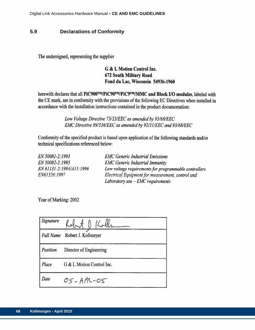
68
Digital Link Accessories Hardware Manual - CE AND EMC GUIDELINES
5.9 Declarations of Conformity
Kollmorgen - April 2010

Digital Link Accessories Hardware Manual - CE AND EMC GUIDELINES
Kollmorgen - April 2010 69
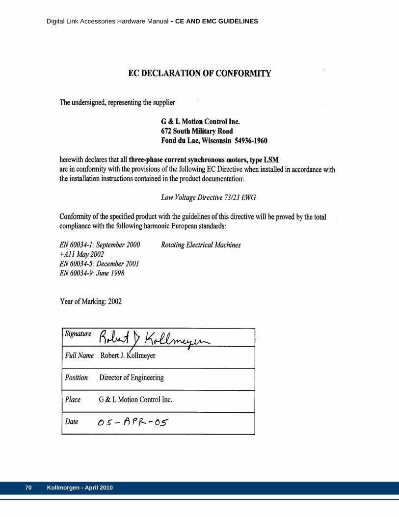
70
Digital Link Accessories Hardware Manual - CE AND EMC GUIDELINES
Kollmorgen - April 2010

Digital Link Accessories Hardware Manual - CE AND EMC GUIDELINES
Kollmorgen - April 2010 71

72
Digital Link Accessories Hardware Manual - CE AND EMC GUIDELINES
Kollmorgen - April 2010

Digital Link Accessories Hardware Manual - OPERATION DETAILS
Appendix A - Operation Details6.1 Introduction
This appendix describes in detail the operation of many of the sub-systems found within the MMC Control and Option Modules.
6.2 DC InputsEach input is guaranteed “on” at 14 to 30 VDC and guaranteed “off” at 0 to 5 VDC (polarity doesn't matter). Its on/off state is converted to a corresponding logic 1 or 0. This logic state is transmitted through the system bus to the application program, which uses these logic states to control program flow. The logic side of the input is optically isolated from the field side.
The shaded blocks in Figure 6-1 below show the limits specified by the IEC. The lines show the maximum and minimum V/I of the inputs in this module. The voltage/current curve in this graph shows that the input module is well within the IEC Type 1 limits.
Figure 6-1: Input Characteristics Compared to IEC Standards
U in VoltsUHMAX 30
UNOM 2425
“ON” REGION
20
UHMIN 15(UTMAX)
10
5
0
-5
.5 2 4 6 8 10 12 14 15ITMIN IHMIN INPUT CURRENT
I inmAMPS
TRANSITION REGION
“OFF” REGION
IMAX
(UTMIN )ULMAX
INPU
T VO
LTA
GE
MIN MAX
Kollmorgen - April 2010 73
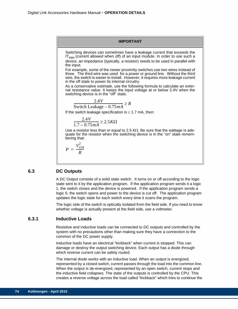
74
Digital Link Accessories Hardware Manual - OPERATION DETAILS
6.3 DC OutputsA DC Output consists of a solid state switch. It turns on or off according to the logic state sent to it by the application program. If the application program sends it a logic 1, the switch closes and the device is powered. If the application program sends a logic 0, the switch opens and power to the device is cut off. The application program updates the logic state for each switch every time it scans the program.
The logic side of the switch is optically isolated from the field side. If you need to know whether voltage is actually present at the field side, use a voltmeter.
6.3.1 Inductive LoadsResistive and inductive loads can be connected to DC outputs and controlled by the system with no precautions other than making sure they have a connection to the common of the DC power supply.
Inductive loads have an electrical “kickback” when current is stopped. This can damage or destroy the output switching device. Each output has a diode through which reverse current can be safely routed.
The internal diode works with an inductive load. When an output is energized, represented by a closed switch, current passes through the load into the common line. When the output is de-energized, represented by an open switch, current stops and the inductive field collapses. The state of the outputs is controlled by the CPU. This creates a reverse voltage across the load called “kickback” which tries to continue the
IMPORTANT
Switching devices can sometimes have a leakage current that exceeds theITmin (current allowed when off) of an input module. In order to use such adevice, an impedance (typically, a resistor) needs to be used in parallel withthe input.For example, some of the newer proximity switches use two wires instead ofthree. The third wire was used for a power or ground line. Without the thirdwire, the switch is easier to install. However, it requires more leakage currentin the off state to power its internal circuitry.As a conservative estimate, use the following formula to calculate an exter-nal resistance value. It keeps the input voltage at or below 2.4V when theswitching device is in the "off" state.
If the switch leakage specification is ≤ 1.7 mA, then:
Use a resistor less than or equal to 2.5 KΩ. Be sure that the wattage is ade-quate for the resistor when the switching device is in the “on” state remem-bering that:
2.4VSwitch Leakage 0.75mA–--------------------------------------------------------------- R≥
2.4V1.7 0.75mA–-------------------------------- 2.5KΩ≥
PVON
2
R----------=
Kollmorgen - April 2010
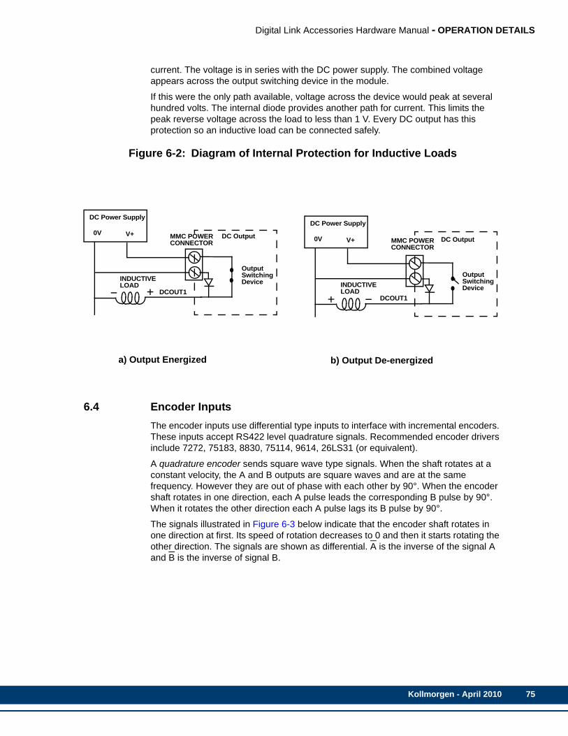
Digital Link Accessories Hardware Manual - OPERATION DETAILS
current. The voltage is in series with the DC power supply. The combined voltage appears across the output switching device in the module.
If this were the only path available, voltage across the device would peak at several hundred volts. The internal diode provides another path for current. This limits the peak reverse voltage across the load to less than 1 V. Every DC output has this protection so an inductive load can be connected safely.
Figure 6-2: Diagram of Internal Protection for Inductive Loads
6.4 Encoder InputsThe encoder inputs use differential type inputs to interface with incremental encoders. These inputs accept RS422 level quadrature signals. Recommended encoder drivers include 7272, 75183, 8830, 75114, 9614, 26LS31 (or equivalent).
A quadrature encoder sends square wave type signals. When the shaft rotates at a constant velocity, the A and B outputs are square waves and are at the same frequency. However they are out of phase with each other by 90°. When the encoder shaft rotates in one direction, each A pulse leads the corresponding B pulse by 90°. When it rotates the other direction each A pulse lags its B pulse by 90°.
The signals illustrated in Figure 6-3 below indicate that the encoder shaft rotates in one direction at first. Its speed of rotation decreases to 0 and then it starts rotating the other direction. The signals are shown as differential. A is the inverse of the signal A and B is the inverse of signal B.
DC Power Supply
0V V+
INDUCTIVELOAD
DCOUT1
a) Output Energized
DC Output
OutputSwitchingDevice
DC Power Supply
0V V+
INDUCTIVELOAD
DCOUT1
b) Output De-energized
DC Output
OutputSwitchingDevice
MMC POWERCONNECTOR MMC POWER
CONNECTOR
Kollmorgen - April 2010 75

76
Digital Link Accessories Hardware Manual - OPERATION DETAILS
Figure 6-3: Signals Transmitted by a Quadrature Encoder with Differential Outputs
The maximum input frequency is 250,000 lines per second, which results in 1,000,000 Feedback Units (FUs) per second.
Figure 6-4: Counting Quadrature Pulses
There is a 24-bit up/down counter for each channel. It is incremented or decremented on each A, B edge. There is also a 24-bit latch associated with each encoder channel.
The module can be programmed so that the counter value is “latched” or stored under one of these conditions:
• an index pulse from the encoder
• a positive or negative transition of the fast input
• the next index pulse after the required transition of the fast input
Each of the five 24-bit latches has a fast 24 VDC input associated with it. Each input is optically isolated. This input is intended to receive a signal from a device other than an encoder. It is typically used for referencing or synchronization purposes.
Fast input characteristics include:
• the detection of a signal occurs faster than it does for the DC inputs in other mod-ules, due to less filtering. Because of this there is also less noise immunity.
• the response to a fast input signal is independent of ladder scan time. The mod-ule can be programmed to latch a position count as soon as this input is detected.
ROTATION SPEED0
A
A
B
B
OUTPUT
B
A
1 2 3 4 5 6 7 8 9 10 11 12 Encoder Count
The module counts positivetransitions at both channel Aand channel B. One quadraturecycle in this case gives4 feedback units.
Kollmorgen - April 2010

Digital Link Accessories Hardware Manual - INDEX
IndexAaddress switches
DL-DIU 40slice I/O coupler 20
analog input port detailsDL-DIU 55
axis I/O port (DL-DIU) 43analog output 50DC input 49DC outputs 47encoder input 51
CCE guidelines 61Compliance
to low voltage directive 61conformance
EMC directive 63low voltage directive 63
conformitydeclaration of 68
connectionsfor EMC compliance 64
contents of the manual 5DDC input connectors
slice I/O coupler 24DC inputs
operationgeneral 73
DC output connectorsslice I/O coupler 26
DC outputsgeneral operation 74inductive loads 74
declaration of conformity 68diagnostic indicator
DL-DIU 39digital link LEDs
DL-DIU 39digital link ports
DL-DIU 41slice I/O coupler 21
DL-DIUaddress switches 40axis I/O port 43
analog output 50DC input 49encoder input 51
axis I/O port DC outputs 47diagnostic indicator 39digital link LEDs 39digital link ports 41front panel details 39I/O and power ports 52
analog input port details 55input port details 54wiring example 55
introduction 37LEDs 39power indicator 39specifications 57
Eelectrical service & maintenance safety 10electro-static discharge 62EMC
modules 66operating environments 62PiC products 63
EMC directiveconformance 63
EMC guidelines 61encoder inputs
general operation 75ESD 62
Ffast transient voltage 62features
slice I/O 13front panel details
DL-DIU 39
Ggrounding
protective earth 8guidelines
CE 61EMC 61
II/O and power ports
DL-DIU 52inductive loads
DC outputs 74input port details
DL-DIU 54inspection
safety 9installation
slice I/O 16
Kollmorgen - April 2010 77

Digital Link Accessories Hardware Manual - INDEX
78
LLED indicators
slice I/O coupler 19LEDs
DL-DIU 39low voltage directive
conformance 63
Mmanual cleaning procedure 11
Ooperation
DC inputs 73DC outputs 74encoder inputs 75safety 10
Ppower connector
slice I/O 23power indicator
DL-DIU 39procedure
manual cleaning 11protective earth
grounding 8RRFI
emission 61immunity 61
Ssafety
after shutdown 9cleaning 11electrical service & maintenance 10inspection 9operating safely 10operation 10signs 8system 7warning labels 8
Sales and Service 80Service 80
signssafety 8
Slice I/O 13slice I/O
coupler details 19features 13installation 16module removal 17power connector 23terminal block operation 18wiring example 27
slice I/O coupleraddress switches 20DC input connectors 24DC output connectors 26digital link ports 21LED indicators 19specifications 35
slice I/O modulesdescription 30limitations and precautions 30types available 30
softwarerequired 5
specificationsDL-DIU 57slice I/O coupler 35
Ttechnical support contacts 6terminal block operation
slice I/O 18
Vvoltage
fast transient 62
Wwarning label
danger, warning, caution 9hazard 8
Web Address 80wiring
for EMC compliance 64wiring example
DL-DIU 55slice I/O 27
Kollmorgen - April 2010

Digital Link Accessories Hardware Manual - INDEX
Kollmorgen - April 2010 79

Sales and ServiceWe are committed to quality customer service. In order to serve in the most effective way, please contact your local sales representative for assistance.
If you are unaware of your local sales representative, please contact us.
North AmericaKollmorgen Customer Support North AmericaE-mail: [email protected]
Phone: In the United States, telephone (800) 558-4808
Outside the United States, telephone (920) 921-7100
Fax: (920) 906-7669
Web site: www.kollmorgen.com
EuropeKollmorgen Customer Support EuropeE-mail: [email protected]
Phone: +44 (0)1525 243-243
Fax: +44 (0)1525 243-244
Web site: www.kollmorgen.com