Embed Size (px)
Citation preview
Application ReportSWRA033E − June 2001 − Revised August 2005
1
Designing With the TRF6900 Single-Chip RF TransceiverCraig Bohren, Matthew Loy, and John Schillinger Mixed-Signal RF
ABSTRACT
This document explains how to operate the TRF6900 single-chip RF transceiver. It describesthe design and selection of the support circuitry present on the evaluation board and providesgeneric design equations for each section to assist you with your specific system designs.
To review operation and design equations for the TRF4900 single-chip RF transmitter, seeapplicable transmitter sections of this document (Section 2).
Contents
1 Introduction 3. . . . . . . . . . . . . . . . . . . . . . . . . . . . . . . . . . . . . . . . . . . . . . . . . . . . . . . . . . . . . . . . . . . . . . . . . 1.1 Description 3. . . . . . . . . . . . . . . . . . . . . . . . . . . . . . . . . . . . . . . . . . . . . . . . . . . . . . . . . . . . . . . . . . . . . . 1.2 Block Diagram/Pinout 4. . . . . . . . . . . . . . . . . . . . . . . . . . . . . . . . . . . . . . . . . . . . . . . . . . . . . . . . . . . . .
2 Transmitter 5. . . . . . . . . . . . . . . . . . . . . . . . . . . . . . . . . . . . . . . . . . . . . . . . . . . . . . . . . . . . . . . . . . . . . . . . . . 2.1 Direct Digital Synthesizer (DDS) 5. . . . . . . . . . . . . . . . . . . . . . . . . . . . . . . . . . . . . . . . . . . . . . . . . . . . 2.2 Clock Frequency Selection 9. . . . . . . . . . . . . . . . . . . . . . . . . . . . . . . . . . . . . . . . . . . . . . . . . . . . . . . .
2.2.1 Calculation of DDS Word 12. . . . . . . . . . . . . . . . . . . . . . . . . . . . . . . . . . . . . . . . . . . . . . . . . . . 2.3 Crystal Specifications 14. . . . . . . . . . . . . . . . . . . . . . . . . . . . . . . . . . . . . . . . . . . . . . . . . . . . . . . . . . . . 2.4 TRF6900 Clock Circuit 15. . . . . . . . . . . . . . . . . . . . . . . . . . . . . . . . . . . . . . . . . . . . . . . . . . . . . . . . . . . 2.5 Local Oscillator 16. . . . . . . . . . . . . . . . . . . . . . . . . . . . . . . . . . . . . . . . . . . . . . . . . . . . . . . . . . . . . . . . . .
2.5.1 Voltage-Controlled Oscillator 16. . . . . . . . . . . . . . . . . . . . . . . . . . . . . . . . . . . . . . . . . . . . . . . 2.5.2 Loop Filter Design 22. . . . . . . . . . . . . . . . . . . . . . . . . . . . . . . . . . . . . . . . . . . . . . . . . . . . . . . . .
2.6 PLL Phase Noise 27. . . . . . . . . . . . . . . . . . . . . . . . . . . . . . . . . . . . . . . . . . . . . . . . . . . . . . . . . . . . . . . .
3 Receiver 29. . . . . . . . . . . . . . . . . . . . . . . . . . . . . . . . . . . . . . . . . . . . . . . . . . . . . . . . . . . . . . . . . . . . . . . . . . . 3.1 Low-Noise Amplifier (LNA) 30. . . . . . . . . . . . . . . . . . . . . . . . . . . . . . . . . . . . . . . . . . . . . . . . . . . . . . . . 3.2 Mixer 30. . . . . . . . . . . . . . . . . . . . . . . . . . . . . . . . . . . . . . . . . . . . . . . . . . . . . . . . . . . . . . . . . . . . . . . . . . 3.3 First IF Amplifier 31. . . . . . . . . . . . . . . . . . . . . . . . . . . . . . . . . . . . . . . . . . . . . . . . . . . . . . . . . . . . . . . . 3.4 Second IF Amplifier and Limiter 31. . . . . . . . . . . . . . . . . . . . . . . . . . . . . . . . . . . . . . . . . . . . . . . . . . . 3.5 Received-Signal-Strength Indicator (RSSI) 31. . . . . . . . . . . . . . . . . . . . . . . . . . . . . . . . . . . . . . . . . . 3.6 FM/FSK Demodulator 31. . . . . . . . . . . . . . . . . . . . . . . . . . . . . . . . . . . . . . . . . . . . . . . . . . . . . . . . . . . .
3.6.1 Calculation of Components for the Demodulation-Tank Circuit for TRF6900 31. . . . . . . 3.7 Low-Pass Filter Amplifier/Post-Detection Amplifier 37. . . . . . . . . . . . . . . . . . . . . . . . . . . . . . . . . . . 3.8 Data Slicer 41. . . . . . . . . . . . . . . . . . . . . . . . . . . . . . . . . . . . . . . . . . . . . . . . . . . . . . . . . . . . . . . . . . . . . . 3.9 Learn and Hold Mode 43. . . . . . . . . . . . . . . . . . . . . . . . . . . . . . . . . . . . . . . . . . . . . . . . . . . . . . . . . . . .
4 PCM-Data Coding Methods 46. . . . . . . . . . . . . . . . . . . . . . . . . . . . . . . . . . . . . . . . . . . . . . . . . . . . . . . . . . 4.1 PCM Code Waveforms 47. . . . . . . . . . . . . . . . . . . . . . . . . . . . . . . . . . . . . . . . . . . . . . . . . . . . . . . . . . .
5 Image Response 48. . . . . . . . . . . . . . . . . . . . . . . . . . . . . . . . . . . . . . . . . . . . . . . . . . . . . . . . . . . . . . . . . . . .
6 Determination of Signal-to-Noise Ratio 48. . . . . . . . . . . . . . . . . . . . . . . . . . . . . . . . . . . . . . . . . . . . . . .

SWRA033E
2 Designing With the TRF6900 Single-Chip RF Transceiver
7 PCB-Board Layout Guidelines 49. . . . . . . . . . . . . . . . . . . . . . . . . . . . . . . . . . . . . . . . . . . . . . . . . . . . . . . 7.1 Clock-Circuit PCB-Layout Considerations 50. . . . . . . . . . . . . . . . . . . . . . . . . . . . . . . . . . . . . . . . . . .
8 FSK-Modulation Theory 50. . . . . . . . . . . . . . . . . . . . . . . . . . . . . . . . . . . . . . . . . . . . . . . . . . . . . . . . . . . . .
9 Required Bandwidth for Transmit and Receive 54. . . . . . . . . . . . . . . . . . . . . . . . . . . . . . . . . . . . . . . .
10 Bit Error Rate 56. . . . . . . . . . . . . . . . . . . . . . . . . . . . . . . . . . . . . . . . . . . . . . . . . . . . . . . . . . . . . . . . . . . . . . .
11 References 57. . . . . . . . . . . . . . . . . . . . . . . . . . . . . . . . . . . . . . . . . . . . . . . . . . . . . . . . . . . . . . . . . . . . . . . . .
List of Figures
1 TRF6900 Functional Block Diagram 4. . . . . . . . . . . . . . . . . . . . . . . . . . . . . . . . . . . . . . . . . . . . . . . . . . . . . . . 2 Transmitter Block Diagram 5. . . . . . . . . . . . . . . . . . . . . . . . . . . . . . . . . . . . . . . . . . . . . . . . . . . . . . . . . . . . . . . 3 TRF6900 DDS/Synthesizer Block Diagram 8. . . . . . . . . . . . . . . . . . . . . . . . . . . . . . . . . . . . . . . . . . . . . . . . . 4 Clock Circuit 15. . . . . . . . . . . . . . . . . . . . . . . . . . . . . . . . . . . . . . . . . . . . . . . . . . . . . . . . . . . . . . . . . . . . . . . . . . . 5 TRF6900 Local Oscillator Functional Block Diagram 16. . . . . . . . . . . . . . . . . . . . . . . . . . . . . . . . . . . . . . . . 6 Voltage-Controlled Oscillator for the TRF6900 ISM Transceiver 17. . . . . . . . . . . . . . . . . . . . . . . . . . . . . . 7 Typical Performance of the VCO 21. . . . . . . . . . . . . . . . . . . . . . . . . . . . . . . . . . . . . . . . . . . . . . . . . . . . . . . . . 8 Typical Second-Order Passive-Loop Filter 22. . . . . . . . . . . . . . . . . . . . . . . . . . . . . . . . . . . . . . . . . . . . . . . . . 9 Typical Lock Time Results for a Step of 10.7 MHz 24. . . . . . . . . . . . . . . . . . . . . . . . . . . . . . . . . . . . . . . . . . 10 Typical Phase Noise Performance of the PLL 25. . . . . . . . . . . . . . . . . . . . . . . . . . . . . . . . . . . . . . . . . . . . . 11 TX Data Rate vs PLL Bandwidth 26. . . . . . . . . . . . . . . . . . . . . . . . . . . . . . . . . . . . . . . . . . . . . . . . . . . . . . . . 12 System Phase-Noise Contributions 27. . . . . . . . . . . . . . . . . . . . . . . . . . . . . . . . . . . . . . . . . . . . . . . . . . . . . . 13 Receiver Block Diagram 29. . . . . . . . . . . . . . . . . . . . . . . . . . . . . . . . . . . . . . . . . . . . . . . . . . . . . . . . . . . . . . . 14 LNA and Mixer Matching Components 30. . . . . . . . . . . . . . . . . . . . . . . . . . . . . . . . . . . . . . . . . . . . . . . . . . . 15 FM Demodulator Block Diagram 31. . . . . . . . . . . . . . . . . . . . . . . . . . . . . . . . . . . . . . . . . . . . . . . . . . . . . . . . 16 Demodulation Tank Circuit 31. . . . . . . . . . . . . . . . . . . . . . . . . . . . . . . . . . . . . . . . . . . . . . . . . . . . . . . . . . . . . 17 Low-Pass Filter Amplifier/Post-Detection Amplifier 37. . . . . . . . . . . . . . . . . . . . . . . . . . . . . . . . . . . . . . . . 18 Low-Pass Filter Amplifier/Post-Detection Amplifier Output Waveform 41. . . . . . . . . . . . . . . . . . . . . . . . 19 AFC Control Loop Block Diagram 41. . . . . . . . . . . . . . . . . . . . . . . . . . . . . . . . . . . . . . . . . . . . . . . . . . . . . . . 20 Data Output at AMP_OUT and RX_DATA Test Points 42. . . . . . . . . . . . . . . . . . . . . . . . . . . . . . . . . . . . . . 21 TRF6900 Wake-Up and Reception of Data 46. . . . . . . . . . . . . . . . . . . . . . . . . . . . . . . . . . . . . . . . . . . . . . . 22 Pulse-Code-Modulation (PCM) Waveforms 47. . . . . . . . . . . . . . . . . . . . . . . . . . . . . . . . . . . . . . . . . . . . . . . 23 USA ISM Band Real vs Image Frequencies 48. . . . . . . . . . . . . . . . . . . . . . . . . . . . . . . . . . . . . . . . . . . . . . 24 FSK-Modulated Output Signal vs Modulating Signal m(t) 50. . . . . . . . . . . . . . . . . . . . . . . . . . . . . . . . . . . 25 Input-Data Signal 53. . . . . . . . . . . . . . . . . . . . . . . . . . . . . . . . . . . . . . . . . . . . . . . . . . . . . . . . . . . . . . . . . . . . . 26 Power Spectral Density of FSK for Pseudorandom Data 54. . . . . . . . . . . . . . . . . . . . . . . . . . . . . . . . . . .
List of Tables
1 Clock Frequency of 25.6 MHz 11. . . . . . . . . . . . . . . . . . . . . . . . . . . . . . . . . . . . . . . . . . . . . . . . . . . . . . . . . . . 2 Frequency Error vs ppm 14. . . . . . . . . . . . . . . . . . . . . . . . . . . . . . . . . . . . . . . . . . . . . . . . . . . . . . . . . . . . . . . . 3 PCM Binary Coding Methods 46. . . . . . . . . . . . . . . . . . . . . . . . . . . . . . . . . . . . . . . . . . . . . . . . . . . . . . . . . . . . 4 Modulation Index h vs Power Spectra 54. . . . . . . . . . . . . . . . . . . . . . . . . . . . . . . . . . . . . . . . . . . . . . . . . . . . .

SWRA033E
3 Designing With the TRF6900 Single-Chip RF Transceiver
1 Introduction
The TRF6900 device integrates radio frequency (RF) with digital and analog technologies toform a frequency-agile transceiver for bidirectional RF data links.
1.1 Description
The TRF6900 device operates as an integrated-transceiver circuit for both the European(868−870 MHz), and the North American (902−928 MHz) ISM bands. This device is expresslydesigned for low-power applications over an operating voltage range of 2.2 V to 3.6 V, and iswell suited for battery-powered operation. A key feature of the TRF6900 transceiver is the use ofa direct digital synthesizer (DDS) to allow agile frequency setting with fine-frequency resolution.The receiver uses single conversion, for use with either 10.7-MHz or 21.4-MHz IF filters.
The TRF6900 supports frequency-shift keying (FSK)-modulated transmission or reception withbit rates up to 115.2 Kbps.

SWRA033E
4 Designing With the TRF6900 Single-Chip RF Transceiver
1.2 Block Diagram/Pinout
Figure 1 shows the TRF6900 transceiver functional block and identifies the input/outputterminals.
DIG
_VC
C
DIG
_GN
D
GN
D
VC
O_T
AN
K1
MO
DE
DD
S_V
CC
TX
_DAT
A
VCO
Direct Digital Synthesizerand
Power-Down LogicLOCKDET
PD_OUT1
PD_OUT2
PD_SET
PLL
PA_GND
PA_OUT
PA_VCC
LNA_GND
LNA_IN
LNA_GND
PLL_VCC
IF2_
IN
DE
M_G
ND
VR
EF
MIX
_IN
MIX
_OU
T
MIX
_GN
D
IF1_
IN
IF1_
OU
T
IF_G
ND
LNA
_OU
T
LNA
_VC
C
MIX
_VC
C
RFMixer
1st IFAmplifier
2nd IFAmplifier/Limiter
FM/FSKDemodulator
DEM_VCC
RSSI_OUT
AMP_IN
AMP_CAP
AMP_OUT
S&H_CAP
DATA_OUT
DATA
CLOCK
STROBE
RSSI
DataSlicer
TRF6900(TOP VIEW)
DEM_TANK
DEM_TANK
VC
O_T
AN
K2
DD
S_G
ND
XO
SC
1
XO
SC
2
PLL_GND
1
2
3
4
5
6
7
8
9
10
11
12 25
26
27
28
29
30
31
32
33
34
35
36
13 14 15 16 17 18 19 20 21 22 23 24
48 47 45 44 43 42 41 40 39 38 3746
Serial Interface
RF BufferAmplifier
LO BufferAmplifier
PowerAmplifier
Data Switch
LPF Amplifier/Post-DetectionAmplifier
LNA
BufferAmplifier
ST
DB
Y
Figure 1. TRF6900 Functional Block Diagram

SWRA033E
5 Designing With the TRF6900 Single-Chip RF Transceiver
2 Transmitter
Figure 2 is a block diagram of the TRF6900 that highlights the transmitter portion of the device.
DIG
_VC
C
DIG
_GN
D
GN
D
VC
O_T
AN
K1
MO
DE
DD
S_V
CC
TX
_DAT
A
VCO
Direct Digital Synthesizerand
Power-Down LogicLOCKDET
PD_OUT1
PD_OUT2
PD_SET
PLL
PA_GND
PA_OUT
PA_VCC
LNA_GND
LNA_IN
LNA_GND
PLL_VCC
IF2_
IN
DE
M_G
ND
VR
EF
MIX
_IN
MIX
_OU
T
MIX
_GN
D
IF1_
IN
IF1_
OU
T
IF_G
ND
LNA
_OU
T
LNA
_VC
C
MIX
_VC
C
RFMixer
1st IFAmplifier
2nd IFAmplifier/Limiter
FM/FSKDemodulator
DEM_VCC
RSSI_OUT
AMP_IN
AMP_CAP
AMP_OUT
S&H_CAP
DATA_OUT
DATA
CLOCK
STROBE
RSSI
DataSlicer
TRF6900(TOP VIEW)
DEM_TANK
DEM_TANK
VC
O_T
AN
K2
DD
S_G
ND
XO
SC
1
XO
SC
2
PLL_GND
1
2
3
4
5
6
7
8
9
10
11
12 25
26
27
28
29
30
31
32
33
34
35
36
13 14 15 16 17 18 19 20 21 22 23 24
48 47 45 44 43 42 41 40 39 38 3746
SerialInterface
RF BufferAmplifier
LO BufferAmplifier
PowerAmplifier
Data Switch
LPF Amplifier/Post-DetectionAmplifier
LNA
BufferAmplifier
ST
DB
Y
Figure 2. Transmitter Block Diagram
2.1 Direct Digital Synthesizer (DDS) [21] [22]
In general, all frequency synthesizers generate one or many frequencies from a frequencyreference, where the synthesized output frequency is related to the reference frequency by aselected ratio. The frequency reference, ƒref (which determines the frequency accuracy), isdivided to set the step size. This step size is in turn multiplied up to a final output frequency.Characteristics such as operating-frequency range, step size, frequency accuracy, phase noise,switching time, and spurious-signal level are parameters that are balanced to yield a finaldesign. The DDS-based synthesizer simplifies these design issues while maintaining the variousperformance requirements.

SWRA033E
6 Designing With the TRF6900 Single-Chip RF Transceiver
The advantages of using a direct digital synthesizer to drive a phase-locked loop include veryfast switching speed and frequency agility with fine frequency resolution, while keeping thedesign simple and economical. The disadvantages of the DDS-based synthesizer are spurious-signal responses and degradation of phase noise outside the loop bandwidth.
Frequency accuracy is determined by the reference source. For the TRF6900, the referencesource is determined by the clock/crystal oscillator circuit. Phase noise in any synthesizer isdegraded by 20 Log N. The DDS allows you to reduce N by operating the phase-detectorfrequency at a much higher reference frequency, while maintaining a finer frequency-resolutionin the final output frequency.
Figure 3 on page 8 shows a block diagram of the TRF6900 DDS and synthesizer components.The basic principle of operation of the DDS is to generate a signal in the digital domain and toreconstruct the waveform in the analog domain by D/A conversion. Generation of the signal inthe digital domain is accomplished by adders and D-type flip-flops. The D-type flip-flops act asstorage devices that change their state when clocked. All arithmetic operations are done using amodulo 2N, where the N bits determine the output-frequency resolution (ƒpd) at the phasedetector as shown in equation (1).
ƒpd
ƒref224
Where ƒpd is the minimum phase-detector input frequency. This is the bit weight of the 20 bit ofthe DDS for the clock frequency ƒref used. The power in 224 represents the number of registersof the DDS accumulator, which is 24 for the TRF6900.
The value of ƒpd is multiplied by N, the prescaler value (user-selectable values of 256 or 512),which yields a minimum frequency-step size (∆ƒ) as shown in equation (2) and (3).
ƒ N ƒpd
or
ƒ N
ƒref
224
As previously mentioned, generation of the signal in the digital domain begins with anaccumulator whose output serves as a phase generator. Control inputs to the accumulator are auser-defined frequency word, and a reference clock used to clock the accumulator and othercircuits (D/A, etc.). The accumulator output is a series of pulsed digital samples, spaced at theclock rate, in the form of a linear ramp. The slope of this ramped signal represents a phase,based on the user-defined inputs.
(1)
(2)
(3)

SWRA033E
7 Designing With the TRF6900 Single-Chip RF Transceiver
The slope of the accumulator output is interpreted as the rate of phase change shown inequations (4) and (5).
d()d(t)
Phase 2 (DDS word)
2N
By taking the derivative of the phase as follows:
Note: This value is in radians.
Where:t 1ƒref and 2ƒ
f(t)
2
Frequency (DDS word) ƒref
224
This yields a digitally-encoded frequency with a waveform made up of pulsed digital samplesspaced at the clock rate and results in a triangular-wave shape.
For example, for a DDS word equal to 2,320,000:
Phase 2 (DDS word)
2N 2
(2, 320, 000)
224
2 [0.1382828] 0.8688563 radians
For a 25.6-MHz clock,
d()d(t)
Where: t 1ƒref
t 3.9063 108 s
d(0.8688565 rad)3.9062 108 s
2.224272 107
Therefore:
f(t)
(2 )
2.2777 107
6.2831853 rad
3.54 106 Hz
An 11-bit digital-to-analog converter (DAC) then converts the generated digital sample (made upof a staircase triangular wave) to an analog form. Due to the quantization processes occurring inthe DAC, the resulting output signal is only an approximation of the ideal signal. The output ofthe DAC contains all the frequency components of the fundamental (that is, harmonics, dataglitches, clock leakage) plus their aliases resulting from the sampling process.
(4)
(5)

SWRA033E
8 Designing With the TRF6900 Single-Chip RF Transceiver
Following the DAC, a sine-shaper circuit is used to minimize DAC-signal glitches, etc. Thesine-shaper circuit is followed by a 4-MHz antialiasing filter, which minimizes sampling spurs dueto the D/A conversion process. The ultimate performance of the DDS is primarily dependent onthe quantization errors due to the D/A process, together with the effects of the antialiasing filterthat follows the DAC.
Accumulator
D/A
Sine-Shaper
4-MHz
Antialiasing
LPF
24-Bit User Serial Data
3.54 MHz
Tx Data
XOR
Phase
Detector
Loop Filter VCO906.24 MHz
3.54 MHz
Clock(fref )
d (φ)/d (t)
Frequency
fo_DDS
/NWhere N = 256
or 512
fout
Note: f ref = 25.6 MHz N = 256
Figure 3. TRF6900 DDS/Synthesizer Block Diagram

SWRA033E
9 Designing With the TRF6900 Single-Chip RF Transceiver
The following paragraphs summarize the general performance of the DDS:
• The length of the accumulator and the clock frequency determine the frequency resolution.The accumulator and the clock rate applied to accumulator circuits determine the number ofspurious components in the output spectrum.
Since the accumulator divides by 2N, it generates a logic-level transition at integer multiplesof the clock frequency. The accumulator increments are defined by the DDS frequency wordand the clock rate. When the accumulator is forced to make a logic-level transition at somefractional rate, the information contained in the accumulator output versus its carry outputproduces a phase error or an instantaneous frequency error. Each overflow represents aspurious component in the final output spectrum of the transmitter (TX) or local oscillator(LO). The number of spurious signals can be greatly reduced by proper selection of the clockfrequency.
Another characteristic parameter of the accumulator is data jitter. Generally this is not anissue in low data-rate applications; however, this may become a concern at higher datarates. Jitter results from the accumulator’s average frequency error due to the digital ramp.You can influence the jitter performance by reducing the ratio of the DDS frequency wordrelative to the accumulator length (224). One possible way to reduce data jitter is theselection of higher input-clock frequencies. As the weight of each accumulator bit isincreased, and thus fewer bits are used in the DDS frequency word, the ratio of the DDSfrequency word to the accumulator length is reduced.
Additional factors that affect data jitter are clock stability and insufficient bandwidth in thereceiver post-detection amplifier.
The clock frequency (due to sampling theory) influences quantization noise power andspurious-signal levels, as well as the number of aliasing spurs contained in the output spectrum.The higher the ƒref /ƒo_DDS ratio, the lower these effects are in the final output spectrum whereƒref is the frequency of the reference clock and ƒo_DDS is the output frequency of the DDS (inphase lock) defined in equation (6).
ƒo_DDS
ƒoutN
ƒout is the output frequency of the VCO where N is the divide-by-N factor with a value of 256 or512. ƒo_DDS is the input comparison frequency to the phase detector of the TRF6900.
As the clock frequency (or sampling frequency) is increased, both the number and level of thespurious products in the output spectrum are reduced, while final frequency resolution isdegraded.
2.2 Clock Frequency Selection [21] [22]
Selection of the clock frequency is key in determining the overall DDS spurious performance.The main issue is to minimize the DDS-generated spurs while allowing the VCO to beprogrammed to decimal numbers with minimum frequency error. The chosen clock frequencymust be sufficiently high that the reference spur frequencies are at large enough offsets from thecarrier frequency and the loop contributes to spur suppression. The following demonstrates theselection of the clock frequency and the determination of the synthesizer final output frequency.
(6)

SWRA033E
10 Designing With the TRF6900 Single-Chip RF Transceiver
Assume an output frequency from a DDS-based synthesizer of 928 MHz. This frequency is thefinal VCO output, not to be confused with the DDS output frequency at the phase detector. Thephase-lock loop (PLL) phase detector has two inputs: a reference frequency from the DDS and asample output from the VCO, which is divided by a prescaler value of 256 or 512(user-selectable). The reference input from the DDS is used to steer and hold the VCO at theoutput frequency that you select (see Figure 3).
For a VCO output of 906.24 MHz, the DDS output frequency is 906.24 MHz/256 = 3.54 MHz.For the PLL to lock the VCO at this frequency, the phase detector reference input from the DDSalso must be 3.54 MHz. The DDS output frequency is effectively multiplied by the prescalervalue being used in the loop. The frequency of operation for the PLL is calculated as shown inequation (7).
ƒout (Prescaler) (DDS value) ƒref
224
(N) (DDS_x) ƒref
224
The DDS is programmed by a 24-bit control register, where the LSB bit weight is 20 and theMSB bit weight is 223. The two most significant bits (bits 22 and 23) are not user-accessible andare set to zero internally. Bits 0 through 21 are used to program the transmitter and receiver tothe frequencies that you choose.
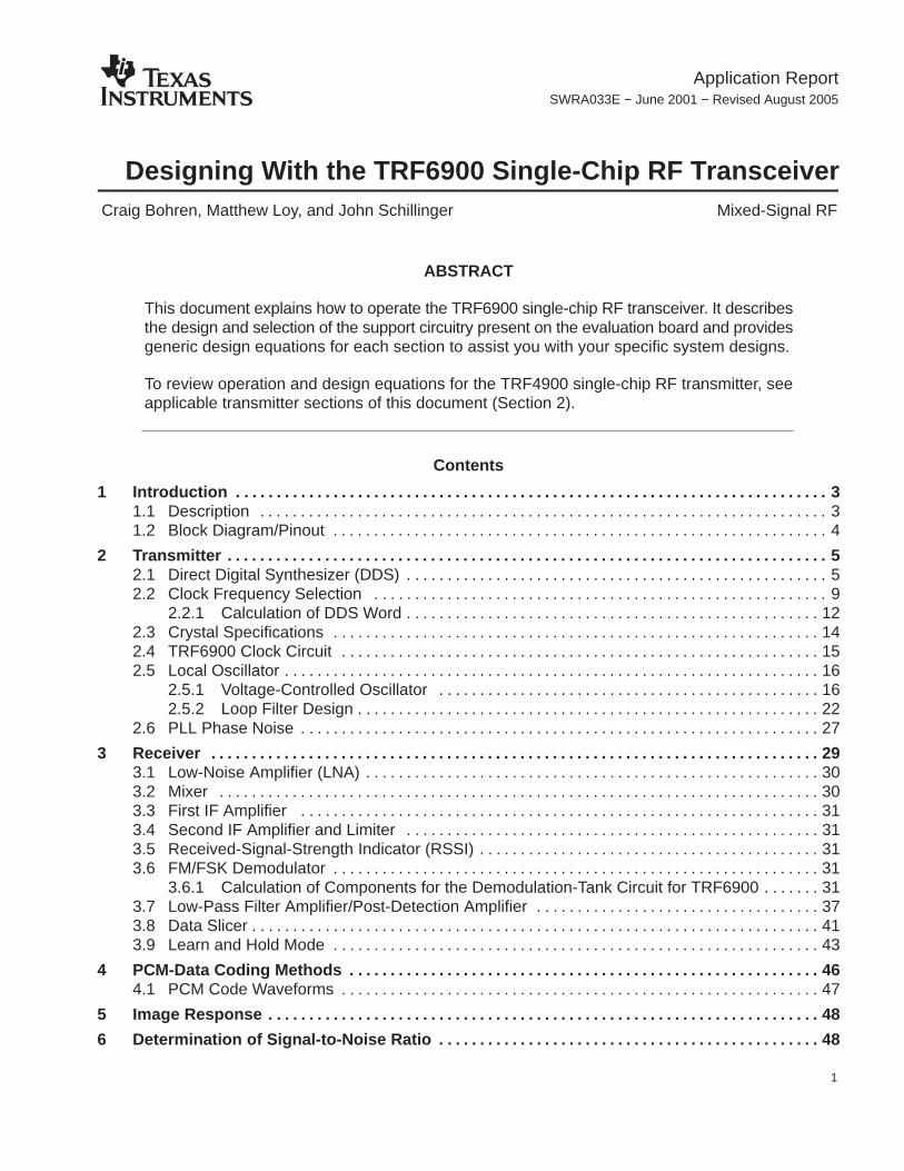
Table 1 shows an example of the DDS register bit weights versus frequency quantization at thephase detector and VCO outputs. At the phase detector, the quantization value of the MSB isƒref /2 (also called the Nyquist frequency). Each additional bit is further divided by 2 to producethe LSB, with ƒout = ƒref /224 (where 24 is the DDS bit-sequence length). As shown in Table 1,ƒref /224 = 25,600,000/16,777,216 = 1.525879 Hz, which represents the LSB frequencyresolution at the phase detector. Note that the LSB is located in the Frequency at PhaseDetector column of Table 1. The frequency resolution at the VCO output is this value(1.525879 Hz) times 256, which is equal to 390.625 Hz. Each bit of the DDS register ismultiplied by the 1.525879-Hz factor. Each effective bit of the Frequency at Phase Detector isfurther multiplied by the selected prescaler value (256) to yield an effective Frequency at VCOquantization value as follows:
Frequency at Phase Detector Frequency at VCO
221 × 1.525879 = 3,200,000 Hz 3,200,000 × 256 = 819,200,000 Hz
220 × 1.525879 = 1,600,000 Hz 1,600,000 × 256 = 409,600,000 Hz··
··
200 × 1.525879 = 1.525879 Hz 1.525879 × 256 = 390.625 Hz
The VCO frequency resolution is 390.625 Hz for this clock frequency. Any clock frequency erroris reflected directly to the final frequency error. Hence, if the clock frequency error is 10 ppm,then the final output frequency will also have a frequency error of 10 ppm.
The PLL filter bandwidth has very little effect on reduction of DDS spurs, since the DDS spursappear very close to the carrier. The objective is to choose a clock frequency that yields aminimum number of DDS spurs while allowing the VCO output to yield a minimum frequencyerror. The recommended clock frequencies of 22, 25.60, and 26 MHz yield minimum spuriouscomponents. To ensure a successful application, you must evaluate the selected clockfrequency for DDS spurious frequency performance versus the final output frequencies used.
(7)
SWRA033E
11 Designing With the TRF6900 Single-Chip RF Transceiver
Table 1. Clock Frequency of 25.6 MHz
BITBIT WEIGHT OF
DDS WORDFREQUENCY AT
PHASE DETECTORFREQUENCY
AT VCOFREQUENCYOF 902 MHz
FREQUENCYOF 915 MHz
FREQUENCYOF 928 MHz
23 = 223 8,388,608 12,800,000Nyquist Frequency
3,276,800,000
22 = 222 4,194,304 6,400,000 1,638,400,000
21 = 221 2,097,152 3,200,000 819,200,000 1 1 1
20 1,048,576 1,600,000 409,600,000
19 524,288 800,000 204,800,000
18 262,144 400,000 102,400,000 1
17 131,072 200,000 51,200,000 1 1
16 65,536 100,000 25,600,000 1 1
15 32,768 50,000 12,800,000 1
14 16,384 25,000 6,400,000 1
13 8,192 12,500 3,200,000 1 1
12 4,096 6,250 1,600,000 1 1
11 2,048 3,125 800,000 1 1
10 1,024 1,562.500 400,000 1 1
9 512 781.250 200,000 1
8 256 390.625 100,000
7 128 195.312,500 50,000
6 64 97.656,250 25,000
5 32 48.828,125 12,500
4 = 24 16 24.414,063 6,250
3 = 23 8 12.207,031 3,125
2 = 22 4 6.103,515,600 1,562.500
1 = 21 2 3.051,757,800 781.250
0 = 20 1 1.525,878,900 390.625
DDS value = 2,309,120 2,342,400 2,375,680
PD Frequency = 2,523,438 3,574,218,800 3,625,000
NOTE: Calculated values are based on N = 256.

SWRA033E
12 Designing With the TRF6900 Single-Chip RF Transceiver
A DDS programming example (using a 25.6-MHz clock) for a VCO output of 915 MHz is detailedas follows:
223 222 221 220 219 218 217 216 215 214 213 212 211 210 209 208 207 206 205 204 203 202 201 200
0 0 1 0 0 0 1 1 1 0 1 1 1 1 1 0 0 0 0 0 0 0 0 0
DDS Word
The value of each bit is summed (221+217+216+215+213+212+211+210+29) to yield a DDS valueof 2,342,400.
The final output frequency is given in equation (8).
ƒout (Prescaler) (DDS value) ƒref
224
(N) (DDS_x) ƒref
224
ƒout (N) (DDS value)
ƒref
16, 777, 216
(256) (2, 342, 400) (25, 600, 000)16, 777, 216
(256) (3, 574, 218.800) 915, 000, 000 Hz
2.2.1 Calculation of DDS Word
The binary value of the DDS word (DDS_x) is calculated by solving equation (7) for the decimalvalue of the DDS word. This value is then converted to hexadecimal format. The hexadecimalvalue can then be written in binary format to complete the conversion.
Equation (8), as stated in the TRF6900 data sheet, is:
ƒout (N) ƒref DDS_x
224
Where:ƒout: VCO output frequencyN: Divide-by ratio of the prescalerƒref: ƒclock system clock frequencyDDS_x: DDS word value in decimal format
Solving equation (9) for the DDS word yields:
DDS_x
ƒoutN
224
ƒref
The following example uses equation (10) to demonstrate the calculation of the A and B wordsfor FSK modulation.
(8)
(9)
(10)
SWRA033E
13 Designing With the TRF6900 Single-Chip RF Transceiver
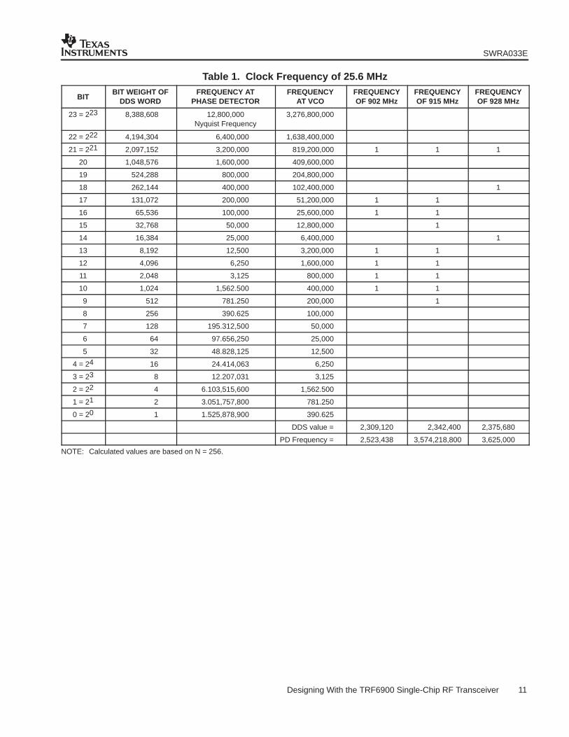
Example 1. Calculation of the DDS Word
Actual FSK modulation is accomplished by using the dedicated FSK frequency deviation registerin the TRF6900. The A and B words then can be used for setting the RX and TX frequenciesand for channel hopping. For illustration purposes only, this example shows how to calculate theDDS_x values of the A and B words for an FSK deviation of 20 kHz if the user were to use the Aand B words to provide FSK modulation. In actual use, the A and B words would be used forFSK deviation only for high deviations that are not supported by use of the deviation register.
Given: FSK system with carrier frequency of 915.0 MHz and 20-kHz FSKdeviation. The system clock is 25.6 MHz, N is 256 for the DDS.
Determine: The DDS_x value of the A and B words
Solution ƒclock = ƒref = 25.6 MHzN = 256ƒout1 = 915.00 MHz A wordƒout2 = 915.02 MHz B word
Calculation of DDS_x value for A word:
The A word has a DDS_x designation of DDS_0.
DDS_0
ƒout1N
224
ƒref
DDS_0
915.00 MHz256 224
25.6 MHz
DDS_0 2.3424 106 decimal
DDS_0 23BE00hex
DDS_0 0010 0011 1011 1110 0000 0000binary
The binary format of DDS_0 is loaded into the A word.
Calculation of DDS_x value for B word.
The B word has a DDS_x designation of DDS_1.
DDS_1
ƒout2N
224
ƒref
DDS_1
915.02 MHz256 224
25.6 MHz
DDS_1 2.342451 106 decimal
(11)
(12)
SWRA033E
14 Designing With the TRF6900 Single-Chip RF Transceiver
Example 1. Calculation of the DDS Word (Continued)
DDS_1 23BE33hex
DDS_1 0010 0011 1011 1110 0011 0011binary
The binary format of DDS_1 is loaded into the B word.
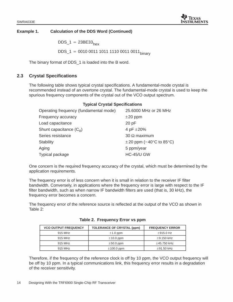
2.3 Crystal Specifications
The following table shows typical crystal specifications. A fundamental-mode crystal isrecommended instead of an overtone crystal. The fundamental-mode crystal is used to keep thespurious frequency components of the crystal out of the VCO output spectrum.
Typical Crystal Specifications
Operating frequency (fundamental mode) 25.6000 MHz or 26 MHz
Frequency accuracy ±20 ppm
Load capacitance 20 pF
Shunt capacitance (Co) 4 pF ±20%
Series resistance 30 Ω maximum
Stability ± 20 ppm (−40°C to 85°C)
Aging 5 ppm/year
Typical package HC-45/U GW
One concern is the required frequency accuracy of the crystal, which must be determined by theapplication requirements.
The frequency error is of less concern when it is small in relation to the receiver IF filterbandwidth. Conversely, in applications where the frequency error is large with respect to the IFfilter bandwidth, such as when narrow IF bandwidth filters are used (that is, 30 kHz), thefrequency error becomes a concern.
The frequency error of the reference source is reflected at the output of the VCO as shown inTable 2:
Table 2. Frequency Error vs ppm
VCO OUTPUT FREQUENCY TOLERANCE OF CRYSTAL (ppm) FREQUENCY ERROR
915 MHz ±1.0 ppm ±915.0 Hz
915 MHz ±10.0 ppm ±9.150 kHz
915 MHz ±50.0 ppm ±45.750 kHz
915 MHz ±100.0 ppm ±91.50 kHz
Therefore, if the frequency of the reference clock is off by 10 ppm, the VCO output frequency willbe off by 10 ppm. In a typical communications link, this frequency error results in a degradationof the receiver sensitivity.

SWRA033E
15 Designing With the TRF6900 Single-Chip RF Transceiver
The frequency error can be held to a minimum by a simple automatic frequency control (AFC).Typical consumer designs use a manual frequency adjustment to align the crystal referencefrequency. Another approach is to measure the reference frequency error, and then use softwarecontrol to add a frequency offset to correct it. If a software frequency offset is used, the crystaltolerance can be degraded to 20, 50, or 100 ppm. The software frequency offset can make thecrystal accuracy independent of final output-frequency error. Another benefit of adding asoftware frequency offset is the reduction in DDS spurs. If the DDS D/A is set to an exactsubmultiple of the clock frequency, then the quantization noise is concentrated at multiples of theoutput frequency. If the clock frequency is offset in the software by the clock crystal’s frequencyerror, the quantization noise is random, resulting in an improvement of DDS spur levels.
An error of 10 to 20 ppm is acceptable for IF bandwidths of 100 kHz or more. If the applicationrequires IF bandwidths of 30 kHz to 50 kHz, a crystal with better than 10-ppm frequencyaccuracy may be required.
2.4 TRF6900 Clock Circuit
The TRF6900 clock-oscillator circuit is shown in Figure 4. This circuit uses the crystal in aparallel-resonant mode.
23
R2
24
R1
XTL1
C2 C1
Figure 4. Clock Circuit
The total phase shift around the loop is 360 degrees, with the inverter providing 180 degrees ofphase shift. Resistor R2 and capacitor C2 provide a 90-degree phase lag, and the crystal andcapacitor C1 provide an additional 90-degree phase lag. In reality, the inverter provides less than180 degrees of phase shift due to its internal capacitance. The R2-C2 combination also providessomething less than 90 degrees of phase shift. The crystal is operating in parallel-resonantmode and acting as an inductor. The crystal-load capacitance makes up the additional phaseshift required for oscillation (360 degrees).
Bias resistor R1 sets the bias point for the inverter, which is typically one-half of Vcc. Low valuesof R1 reduce the loop gain and disturb the phase of the feedback network. Typical values for R1are 1 MΩ to 5 MΩ.
Crystal-drive resistor R2 is used to limit the crystal drive level by forming a voltage dividerbetween R2 and C2. To verify that the maximum operating supply voltage does not overdrive thecrystal, observe the output frequency as a function of voltage at terminal 23. Under properoperating conditions, the frequency should increase slightly (a few ppm) as the supply voltageincreases. If the crystal is being overdriven, an increase in supply voltage causes a decrease infrequency; if this happens, increase the value of R2. In addition, the value of R2 must besufficiently low to ensure that the oscillator starts at a few tenths of a volt below the minimumoperating voltage.

SWRA033E
16 Designing With the TRF6900 Single-Chip RF Transceiver
Ideally, capacitor C2 together with drive resistor R2 provide 90 degrees of phase shift and set thecrystal-drive level. Large values of C2 tend to stabilize the oscillator against variations in VCC,while also reducing any overtone activity of the crystal. Capacitor C1 and the internal impedanceof the crystal provide an additional 90 degrees of phase shift. Large values of C1 reduce loopgain while increasing frequency stability. The series sum of capacitor C1, the crystal’s shuntcapacitance (Co), and the input capacitance of the inverter gate make up the crystal’s loadcapacitance. For increased stability, the load capacitance of the crystal should have a typicalvalue of approximately 20 to 30 pF.
2.5 Local Oscillator
The local oscillator (LO) of the TRF6900 ISM transceiver is a phase-locked loop (PLL) consistingof an on-chip DDS-based frequency synthesizer, an external passive-loop filter, and avoltage-controlled oscillator (VCO). The general functional block diagram of the local oscillator isshown in Figure 5.
Direct DigitalSynthesizer
(DDS)
DigitalInterface ÷ N
ω1 PhaseFrequencyDetectorω2
ChargePump
LoopFilter
Oscillator VaractorLC Tank
fout
θer
TRF6900Local Oscillator Block
Xtal Oscillator(CLOCK)
Clock,Data, Strobe
Figure 5. TRF6900 Local Oscillator Functional Block Diagram
The following sections detail the design considerations for the TRF6900 phase-lockedloop (PLL).
2.5.1 Voltage-Controlled Oscillator
2.5.1.1 Varactor LC Tank Design
Figure 6 describes the VCO of the TRF6900 ISM transceiver, the on-chip oscillator, and anexternal differential varactor LC tank. As shown in Figure 6, the resonant frequency of the tank isgiven in equation (13).
ƒTANK 1
2 LCTOTAL
The total capacitance CTOTAL of equation (13) is defined in equation (14).
CTOTAL C5 1
1C34
1
C34
1CVR1
1
CVR2
where C34 = C3 = C4
(13)
(14)

SWRA033E
17 Designing With the TRF6900 Single-Chip RF Transceiver
RC3
C4
C5LCVR1
CVR2
R
|ZIN|fout
Oscillator
Varactor LC Tank
Vtune
100 kΩR
13
14
TRF6900
Figure 6. Voltage-Controlled Oscillator for the TRF6900 ISM Transceiver
At the resonant frequency, the required inductor value for the differential tank shown in Figure 6is calculated in equation (15).
L 12
ZINQP
QLOADED ZIN
2ƒ QP
Where:|ZIN|: Input impedance of the oscillatorQLOADED: Quality factor of the tankQP: Quality factor of the inductorƒ: Desired resonant frequency
To maximize the frequency tuning range of the tank via the varactor, equation (17) dictates that asmall value for the capacitor C5 must be chosen, and capacitors C3 and C4 must be as large aspossible. With C5 small, the C5 term in equation (17) may be negligible. If C3 and C4 are as
large as possible, the terms 1
C3 and
1C4
are also negligible. Therefore, the variation of CTOTAL
would be dominated by CVR1 and CVR2.
Note that the stray capacitance due to the printed-circuit board (PCB) layout is virtually inparallel with the total capacitance of the tank, and does not affect its resonant frequency.Capacitor C5 must be carefully chosen to include the stray capacitance. If the stray capacitancestrongly affects the resonant frequency of the tank, the value of C5 may be reduced throughexperimentation with the actual circuit on the PCB.
Assuming that C34 = C3 = C4, and CVR = CVR1 = CVR2, the relationship of capacitors C34 andCVR is described in equation (16).
CVR
C34 2CTOTAL C5
C34 2CTOTAL C5
(15)
(16)

SWRA033E
18 Designing With the TRF6900 Single-Chip RF Transceiver
Due to the availability of the tuning capacitance range of the varactor versus the available tuningvoltage, capacitor C34 is arbitrarily chosen at the center frequency of the desired frequencyrange. The typical value of capacitor C34 needs to satisfy the following condition, as shown inequation (17).
C34 2 CTOTAL C5
Remember that the value of capacitor C34 should be as large as possible; thus the 1
C34 term in
equation (14) is negligible. Subsequently, the variation of CTOTAL is then dominated by CVR.
In any application where the TRF6900 is powered up continuously in either TX or RX modewithout periodically going into STBY mode, it is recommended that a 100-kΩ resistor be addedto the VCO tank from either terminal 13 or terminal 14 to ground to ensure the long-term stabilityof the Vtune voltage.
The addition of the 100-kΩ resistor to the VCO tank tends to shift the operating frequency of theVCO downward and decrease KVCO. Thus, after calculation of the VCO components some finetuning may be needed to re-center the tuning range.
2.5.1.2 VCO Sensitivity
Assuming that the capacitance of the varactor varies linearly with the tuning voltage, thesensitivity of the VCO is defined in equation (18).
KVCO ƒ
Vtune
where ∆ƒ = | ƒ1 − ƒ2 |, and ∆Vtune = | Vtune at ƒ1 − Vtune at ƒ2 |
2.5.1.3 Numerical Calculation
The VCO of the TRF6900 initially is designed to operate between 880 MHz and 950 MHz with atuning voltage range of less than 0.3 V to approximately 3 V. The input impedance |ZIN| of theoscillator between terminals 13 and 14 is approximately 1400 Ω. The loaded Q of the tank,QLOADED, must be equal to or greater than 10. The selected inductor (LQW1608A series frommuRata) has a quality factor QP of approximately 80 at 915 MHz.
The required inductor for the tank is calculated from equation (15) as:
L 12
ZINQP
QLOADED ZIN
2ƒ QP
12
14008010 1400
2 3.1416 915e6 80 10.65 nH
Choose L = 10 nH, a standard value.
(17)
(18)

SWRA033E
19 Designing With the TRF6900 Single-Chip RF Transceiver
From equation (13), the required total capacitance (CTOTAL) is:
At ƒ1 880 MHz : CTOTAL_ƒ1
1
(2 880e6)2 10e9 3.271 pF
At ƒc 915 MHz : CTOTAL_ƒc
1
(2 915e6)2 10e9 3.025 pF
At ƒ2 950 MHz : CTOTAL_ƒ2
1
(2 950e6)2 10e9 2.807 pF
To maximize the frequency tuning range of the tank via the varactors, the capacitor C5, whichincludes any PCB stray capacitance, is chosen to be 2.2 pF for this calculation and, fromequation (16), C34 is chosen to be 3.3 pF to mate with a varactor having the followingcharacteristics:
At Vtune 0.5 V : CVR 3.3e12 2(3.271e12 2.2e12)
3.3e12 2(3.271e12 2.2e12) 6.103 pF
At Vtune 2 V : CVR 3.3e12 2(2.807e12 2.2e12)
3.3e12 2(2.807e12 2.2e12) 1.919 pF
An SMV1247 varactor from Alpha Industries is chosen. This varactor has the followingcharacteristics:
CVR ≈ 8.50 pF at VR = 0.10 VCVR ≈ 7.50 pF at VR = 0.25 VCVR ≈ 3.66 pF at VR = 1.25 VCVR ≈ 1.88 pF at VR = 2.00 VCVR ≈ 0.90 pF at VR = 3.00 V
Note that the PCB stray capacitance is unknown, difficult to predict, and varies with operatingfrequency. Therefore, empirical measurement may be required to define the value of C5.
Verification:
With selected values, the total capacitance of the tank is calculated using equation (14) as:
CTOTAL 3.39 pF
At ƒtune 0.10 V :
CTOTAL 2.2e12 1
13.3e12
13.3e12
17.5e12
17.5e12
3.346 pF
At ƒtune 0.25 V :
CTOTAL 2.2e12 1
13.3e12
13.3e12
11.88e12
11.88e12
2.799 pF
At ƒtune 2.00 V :
CTOTAL 2.55 pF
At ƒtune 3.00 V :
SWRA033E
20 Designing With the TRF6900 Single-Chip RF Transceiver
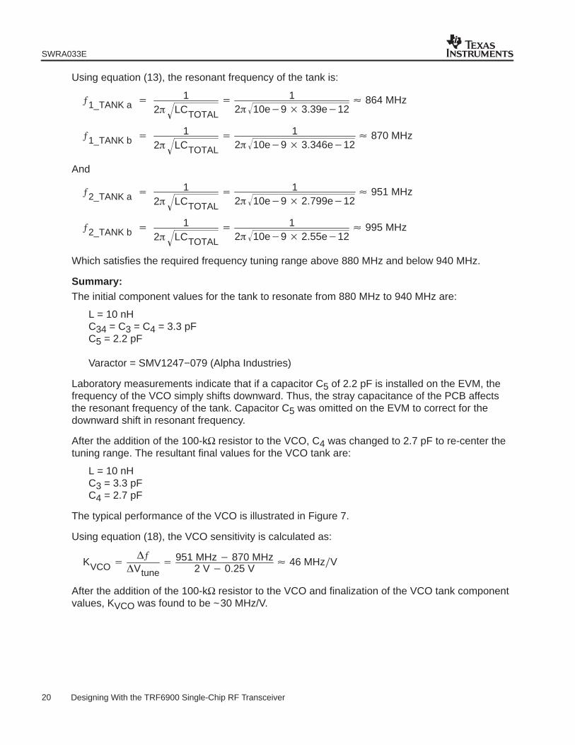
Using equation (13), the resonant frequency of the tank is:
ƒ1_TANK a 1
2 LCTOTAL
12 10e9 3.39e12
864 MHz
ƒ1_TANK b 1
2 LCTOTAL
12 10e9 3.346e12
870 MHz
And
ƒ2_TANK a 1
2 LCTOTAL
12 10e9 2.799e12
951 MHz
ƒ2_TANK b 1
2 LCTOTAL
12 10e9 2.55e12
995 MHz
Which satisfies the required frequency tuning range above 880 MHz and below 940 MHz.
Summary:The initial component values for the tank to resonate from 880 MHz to 940 MHz are:
L = 10 nHC34 = C3 = C4 = 3.3 pFC5 = 2.2 pF
Varactor = SMV1247−079 (Alpha Industries)
Laboratory measurements indicate that if a capacitor C5 of 2.2 pF is installed on the EVM, thefrequency of the VCO simply shifts downward. Thus, the stray capacitance of the PCB affectsthe resonant frequency of the tank. Capacitor C5 was omitted on the EVM to correct for thedownward shift in resonant frequency.
After the addition of the 100-kΩ resistor to the VCO, C4 was changed to 2.7 pF to re-center thetuning range. The resultant final values for the VCO tank are:
L = 10 nHC3 = 3.3 pFC4 = 2.7 pF
The typical performance of the VCO is illustrated in Figure 7.
Using equation (18), the VCO sensitivity is calculated as:
KVCO ƒ
Vtune
951 MHz 870 MHz2 V 0.25 V
46 MHzV
After the addition of the 100-kΩ resistor to the VCO and finalization of the VCO tank componentvalues, KVCO was found to be ~30 MHz/V.

SWRA033E
21 Designing With the TRF6900 Single-Chip RF Transceiver
3SA2SA
3VIEW2VIEW3VIEW
1AVG2VIEW
3SA
VBW 1 MHzRBW 1 MHz
Span 150 MHzCenter 915 MHz 15 MHz
SWT 5 ms
RF Att 30 dBRef Lvl0 dBmRef Lvl0 dBm Unit dBm
1SA2SA
A
−120
−110
−100
−90
−80
−70
−60
−50
−40
−30
−20
−10
01
23
Marker 1 [T1]−7.13 dBm
869.65931864 MHz
1 [T1] −7.13 dBm869.65931864 MHz
2 [T1] −67.86 dBm915.00000000 MHz
3 [T1] −64.44 dBm960.00000000 MHz
Date: 17.MAR.2000 23:23:53
Figure 7. Typical Performance of the VCO

SWRA033E
22 Designing With the TRF6900 Single-Chip RF Transceiver
2.5.2 Loop Filter Design
Figure 8 shows a typical second-order passive loop filter configuration commonly used withcurrent-mode charge-pump frequency synthesizer devices.
C1 R2
C2
VCO
SpeedupMode
ICP Vtune
TRF6900
Rbias
Figure 8. Typical Second-Order Passive-Loop Filter
The component values for this filter are given by the following equations:
C1
12
KPD KVCOc
2 N
1 c 22
1 c 12
C2 C1 21
1
R2
2C2
Where:
KPD:Phase-detector gain, 4 ICP
; Arad
ICP: ICP 1.28Rbias
KVCO: VCO gain, 2ƒ
Vtune;
radsV
N: Divider constantRbias: Bias resistor connected to terminal 8ωc: Loop bandwidth in radians/sBN: BN ≈ 2 × data rate, Hz
τ1: 1 sec tan
c
τ2: 2 1
c2 1
Φ: Phase margin in radians
(19)
(20)
(21)

SWRA033E
23 Designing With the TRF6900 Single-Chip RF Transceiver
2.5.2.1 Numerical Calculation of the Second Order Loop Filter
The divider is selected as N = 256. Rbias is selected to be 300 kΩ. The VCO gain was measuredas 30 MHz/V.
The loop bandwidth in radians per second is derived in equation (22).
c 2BN
c 2 20 103 radianss
where BN is the recommended loop bandwidth.
The minimum loop bandwidth, in Hertz, must be equal to or greater than the data rate. As a ruleof thumb, the loop bandwidth is set to approximately 1.3 to 2 times the data rate. For thisexample, the loop bandwidth, BN, was set to 20 kHz, which is twice the data rate (data rate = 10kHz, bit rate = 20 kbps). A loop bandwidth of 20 kHz should support data rates up to 20 kHz (bitrate = 40 kbps).
The phase margin is set to 50 degrees; thus: 50
180 0.873 radians.
1 sec tan
c 2.896 106
2 1
c2 1
2.186 105
From equation (19), capacitor C1 becomes 92 pF.
From equation (20), capacitor C2 is found to be 655 pF.
Finally, from equation (21), resistor R2 is calculated to be 33 kΩ.
Because the calculated component values are not standard, the following standard values areinitially selected:
C1 = 100 pFC2 = 650 pFR2 = 33 kΩ
Next, the loop values were checked with the following equations:
ƒn natural loop frequency 1
2
KPD KVCON (C1C2)
; Hz
ζ loop damping factor R2 C2
2 2ƒn
ƒc calculated loop bandwidth 2 ζ ƒn; Hz
c 2ƒc
The initial values of the loop components were optimized to minimize phase noise and spuriousresponses, to adjust the loop bandwidth closer to 20 kHz, and to obtain a damping factor closeto 1. Normally, the damping factor is set between 0.707, for best switching speed, and 1, for bestloop stability. For a damping factor of ζ = 1, the final values selected for the loop filter were:
(22)

SWRA033E
24 Designing With the TRF6900 Single-Chip RF Transceiver
C1 = 100 pFC2 = 750 pFR2 = 39 kΩ
For data rates of 57.6 kbps or higher, an Rbias resistor of 200 kΩ is recommended in order tohave sufficient charge-pump gain.
Figure 9. Typical Lock Time Results for a Step of 10.7 MHz

SWRA033E
25 Designing With the TRF6900 Single-Chip RF Transceiver
Figure 10. Typical Phase Noise Performance of the PLL
The loop filter receives two inputs from the phase detector: normal mode (terminal 10) andspeed-up mode (terminal 9).
Normal mode is used to fine steer and hold the VCO at the commanded frequency.
The speedup mode provides a fast coarse steering of the VCO with the APLL (accelerationfactor for PLL) setting. The TRF6900 software allows you to adjust this value as required. Thedefault value is 140 pulses of acceleration; lower values of APLL slow the lock time. When lowervalues of APLL are used, typical applications are in narrow-band FSK to avoid lock-timeovershoot.
Figure 11 details the relationship between the synthesizer loop bandwidth and the TX data rate.For a DDS-based synthesizer, the loop bandwidth must be at least equal to, and preferablygreater than, the TX data rate (or modulation rate). As a rule of thumb, for the TRF6900, theloop bandwidth, in Hertz, is set to approximately 1.3 to 2 times the data rate. If this requirementis not met, the FSK output spectrum is distorted. If the loop bandwidth is much less than the TXdata rate, no modulation will be present on the output spectrum. Thus, the maximum user datarate determines the minimum loop bandwidth for the application.

SWRA033E
26 Designing With the TRF6900 Single-Chip RF Transceiver
928 MHz
Reference Clock
Phase Det Loop Filter
Prescaler256 / 512
3.625 MHz
3.625 MHz
Modulation
Classical Synthesizer
VCO
928 MHzPhase Det Loop Filter
Prescaler256 / 512
3.625 MHz
3.625 MHz
DDS-Based Synthesizer
VCO
DDS ModulationReference Clock
Figure 11. TX Data Rate vs PLL Bandwidth
For the classical synthesizer, which directly modulates the VCO, the modulation rate must begreater than the bandwidth of the PLL loop filter; otherwise, the PLL tends to track out themodulation. With low-frequency modulation, the bandwidth of the PLL loop filter becomesnarrow and the resultant lock time of the PLL loop becomes large. Another source of error iswhen the modulation data contains long strings of ones or zeroes. The problem with a longstring of ones or zeroes in the receiver section is that the sample and hold capacitor, whichprovides the reference level for the data slicer, is not charged to the proper level. Therefore, aManchester encoding scheme must be used to minimize the modulation tracking problem whenthe classical synthesizer is used. See Sections 3.8, 3.9, 4, and 4.1 for a more detailedexplanation.
A DDS-based synthesizer, as used in the TRF6900, is modulated outside the loop by modulatingthe reference frequency. As stated previously, the PLL loop bandwidth must be equal to orgreater than the modulation rate applied to the synthesizer. The advantage of using aDDS-based synthesizer is that as the PLL loop bandwidth is increased for higher data rates, locktime decreases and close-in phase noise performance improves. The trade-off is that spursuppression and rejection of out-of-band phase noise degrade as the PLL loop-filter bandwidthis increased.

SWRA033E
27 Designing With the TRF6900 Single-Chip RF Transceiver
2.6 PLL Phase Noise
−70
−20
−40
−120
−60
−100
−80
−90
−110
−50
−30
10 100 1k 10k 100k 1M 10M
System Contributions to Phase Noise
Offset Frequency − Hz
Noise Contribution From:Reference Oscillator, Phase-FrequencyDetector, 1/f Noise, Charge Pumps and V ccBypassing.
PLL In-Band Noise Contributions, Including ReferenceOscillator Noise Multiplied Up By the Prescaler.
VCO Phase Noise
Pha
se N
oise
− d
Bc/
Hz
Figure 12. System Phase-Noise Contributions

SWRA033E
28 Designing With the TRF6900 Single-Chip RF Transceiver
A typical phase-noise plot, illustrated in Figure 12, comprises three main groups of noisecontributors (shown from left to right in order of increasing frequency-offset from thefundamental).
• The IC phase/frequency detector (PFD), charge pump (CP), reference oscillator, 1/f noise,and Vcc bypassing
• The PLL loop filter
• The VCO
The close-in (close to the origin or zero offset) phase noise (1/f noise) is dependent upon thephase/frequency detector and charge pump. The center of the phase-noise plot (in-band) isdependent on the PLL loop bandwidth. The tail of the phase-noise plot (out-of-band) isdependent on the VCO.
Given the above information, the following conclusions can be stated about the effects ofchanging the loop filter bandwidth for a PLL.
• Wide PLL loop-filter bandwidth has the following results:
− Decreased close-in phase noise
− Fast lock time
− Degraded (less) reference spur suppression
− Degraded suppression of out-of-band phase noise (high out-of-band phase noise)
• A narrow PLL-filter bandwidth has the following results: (opposite of above)
− Degraded (increased) close-in phase noise
− Slow lock time
− Increased reference spur suppression
− Increased suppression of out-of-band phase noise
DDS spurs are usually close-in, inside the PLL loop bandwidth, and thus can not be suppressedby the PLL loop filter. However, if we narrow the loop filter bandwidth we can reduce thelikelihood that in-band DDS spurs occur. Only proper selection of the reference clock frequencyhas an influence on DDS spurs. Reference spurs, on the other hand, are generated at integermultiples of the phase-detector input-frequency offset from the carrier frequency and can befiltered by the PLL loop filter.

SWRA033E
29 Designing With the TRF6900 Single-Chip RF Transceiver
3 ReceiverThe receiver on the TRF6900 is intended to be used as a single-conversion FSK receiver. Thereceiver is composed of a low-noise amplifier (LNA), mixer, IF amplifier, limiter, an FM/FSKdemodulator with an external LC-tank circuit, and a data slicer. Figure 13 is a block diagram ofthe TRF6900 that highlights the receiver portion of the device.
DIG
_VC
C
DIG
_GN
D
GN
D
VC
O_T
AN
K1
MO
DE
DD
S_V
CC
TX
_DAT
A
VCO
Direct Digital Synthesizerand
Power-Down LogicLOCKDET
PD_OUT1
PD_OUT2
PD_SET
PLL
PA_GND
PA_OUT
PA_VCC
LNA_GND
LNA_IN
LNA_GND
PLL_VCC
IF2_
IN
DE
M_G
ND
VR
EF
MIX
_IN
MIX
_OU
T
MIX
_GN
D
IF1_
IN
IF1_
OU
T
IF_G
ND
LNA
_OU
T
LNA
_VC
C
MIX
_VC
C
RF Mixer
1st IFAmplifier
2nd IFAmplifier/Limiter
FM/FSKDemodulator
DEM_VCC
RSSI_OUT
AMP_IN
AMP_CAP
AMP_OUT
S&H_CAP
DATA_OUT
DATA
CLOCK
STROBE
RSSI
DataSlicer
TRF6900(TOP VIEW)
DEM_TANK
DEM_TANK
VC
O_T
AN
K2
DD
S_G
ND
XO
SC
1
XO
SC
2
PLL_GND
1
2
3
4
5
6
7
8
9
10
11
12 25
26
27
28
29
30
31
32
33
34
35
36
13 14 15 16 17 18 19 20 21 22 23 24
48 47 45 44 43 42 41 40 39 38 3746
Serial Interface
RF BufferAmplifier
LO BufferAmplifier
PowerAmplifier
Data Switch
LPF Amplifier/Post-DetectionAmplifier
LNA
BufferAmplifier
ST
DB
Y
Figure 13. Receiver Block Diagram

SWRA033E
30 Designing With the TRF6900 Single-Chip RF Transceiver
3.1 Low-Noise Amplifier (LNA) [22]The low-noise amplifier (LNA) has a typical gain of 13 dB and a typical noise figure of 3.3 dB.Two operating modes are available for the LNA: normal and low-gain. The normal mode isselected for maximum receiver input sensitivity at low RF input levels. If high RF input levels areto be applied to the LNA, the low-gain mode should be selected.
3.2 Mixer [22]The mixer is a conventional double-balanced Gilbert-cell mixer. The mixer is designed to operatewith the on-chip VCO. When an external LO is desired, an LO drive level of approximately–10 dBm is applied to the VCO input terminal 14 (VCO_TANK2).
The mixer output impedance at terminal 44 (MIX_OUT) is 330 Ω. This impedance allows aceramic filter with a 330-Ω impedance to be connected directly to terminal 44 (MIX_OUT).Figure 14 shows the LNA and mixer matching circuit components used on the evaluation board.See the TRF6900 Evaluation Board User’s Guide, literature number SWRU001, for anexplanation of its jumper settings.
LNA_IN
MIX
_IN
MIX
_OU
T
LNA
_VC
C
RF Mixer
2
48 45 4446
RF BufferAmplifier
LNA
MIX
_VC
C
L610 nHLQW1608
C201000 pF
C16100 pF
C174.7 pF
J4RX_IN
R610 Ω
VCC1
C120.1 µF
C40.1 µF
L28.2 nHLQW1608
C51000 pF
1
J2LNA_OUT/MIX_IN
2
C61 pF
3
C910 pF
LNA
_OU
T
47
R20 Ω
JP2
L418 nHLQW1608
C130.1 µF
R510 Ω
VCC1
3
2
1
R10 Ω
C30.1 µF
JP1
1st IF Input, Terminal 42
When Installed, Capacitor C3 is Used to Bypass BPF1 C2
120 pFC1
1000 pF
BPF1
L32.2 µHLQS33N2R2G04M00
J1MIX_OUT/1st IF_INPUT
C1, C2, and L 3 Are Mixer-Output Match for 10.7 MHz
To Internal VCO
Figure 14. LNA and Mixer Matching Components

SWRA033E
31 Designing With the TRF6900 Single-Chip RF Transceiver
3.3 First IF Amplifier [22]
The first IF amplifier has a typical gain of approximately 7 dB, and input and output impedancesof 330 Ω. The purpose of the IF amplifier is to amplify the output waveform from the mixer. Thefirst IF amplifier may be bypassed on the TRF6900.
3.4 Second IF Amplifier and Limiter [22]
The second IF amplifier has a typical gain of approximately 80 dB, and an input impedance of330 Ω. A voltage level of 32 µV is required at terminal 39 (IF2_IN) to generate a limited signal atthe limiter output. The output of the limiter is internally connected to the FM/FSK demodulator.
The limiter is internally connected to the output of the second IF amplifier. The function of thelimiter circuit is to remove amplitude variations from the IF waveform. Amplitude variations in theIF waveform must be removed since the demodulator circuit responds to amplitude variations aswell as frequency variations in the IF waveform. When the demodulator responds to amplitudevariations, the receiver sensitivity is decreased and the distortion in the demodulated waveformis increased.
3.5 Received-Signal-Strength Indicator (RSSI) [22]
The received-signal-strength Indicator (RSSI) output voltage at terminal 33 (RSSI_OUT) isproportional to the RF limiter input level. The slope of the RSSI circuit is typically 19 mV/dB for afrequency range from 10 MHz to 21.4 MHz.
The received-signal-strength indicator is a summing network with inputs from the second IFamplifier and limiter circuits. This summing network produces a voltage which is used to indicatereceived-signal strength. The output voltage of the summing network is a logarithmic function ofthe received signal.
3.6 FM/FSK Demodulator [22] [6]
A quadrature-demodulator circuit is used, as shown in Figure 15.
Low-Pass FilterVo (t)
Vθ (t)Phase-Shift Network With−90° Phase Shift at f c
SFM (t)Input FM Signal
Figure 15. FM Demodulator Block Diagram
The phase-shift network is an external RLC-tank circuit. The low-pass filter amplifier/post-detection amplifier performs the low-pass filter function.
3.6.1 Calculation of Components for the Demodulation-Tank Circuit for TRF6900
R710 kΩ
L52.2 µH
C14100 pF
35
34
VINVOUT
C150 to 3 pF(Optional)
Figure 16. Demodulation Tank Circuit
SWRA033E
32 Designing With the TRF6900 Single-Chip RF Transceiver
The demodulation-tank circuit is shown in Figure 16. The bandwidth of the demodulation tankcircuit must be greater than the bandwidth of the IF filters used. As a rule of thumb, thedemodulation tank circuit bandwidth BWt must be set to 1.5 times the IF filter bandwidth. Thecomposite bandwidth of the IF filter or filters is determined in equation (23).
BWComp 1
1BW2
1
1
BW22
Where:BWComp: Composite bandwidth of the IF filter(s)BW1: Bandwidth of the first IF filterBW2: Bandwidth of the second IF filter
NOTE: If only one IF filter is used, the composite bandwidth BWComp is equal to the single filter bandwidth.
The Q of the IF filters must then be determined:
QIF
ƒcBWComp
Where:QIF: Q of the IF circuitƒc: Center frequency of the IF chainBWComp: Composite bandwidth of the IF filters
The quality factor QT of the demodulation tank circuit is equal to:
QT
ƒc1.5 BWComp
Where:QT: Q of the demodulation-tank circuitƒc: Center frequency of the IF chainBWComp: Composite bandwidth of the IF filters
The quality factor QT of the demodulation tank circuit is also equal to:
QT
QIF1.5
The inductor chosen for the demodulation tank circuit determines the quality factor of thedemodulation tank circuit (QT), because inductors have low values of Q compared to capacitors.The inductor is chosen to have as high a value of Q as possible to properly resonate with thecapacitor.
If the inductor chosen has a Q value higher than QIF (calculated from equation (26)), the Q ofthe demodulation tank circuit must be decreased. The addition of a resistor in parallel with theinductor decreases the Q of the demodulation-tank circuit (QT).
(23)
(24)
(25)
(26)

SWRA033E
33 Designing With the TRF6900 Single-Chip RF Transceiver
The procedure for decreasing the QT of the demodulation tank is as follows:
• Determine QIF using equations (23) and (24).
• Determine QT using equation (25) or (26).
• Use the following equations to choose an inductor and a capacitor to resonate at the properIF frequency:
The IF frequency fc is known. The value of the inductor L is chosen for a high Q value.
The resistive part of the inductor impedance is calculated using equation (27).
Rind Qind 2 ƒc L
Where:Rind:Resistive part of the inductor impedanceQind:Q of the inductorƒc: IF frequencyL: Value of the inductor
Capacitor C is then calculated using equation (28).
C 1
4 2 ƒ2
c L
Where:C: Value of the capacitorƒc: IF frequencyL: Value of the inductor
The resistive part of the tank impedance Rtank is calculated using equation (29).
Rtank QT 2 ƒc L
Where:QT: Q of the demodulation-tank circuitƒc: IF frequencyL: Value of the inductor
The resistor Rext required to decrease the Q of the demodulator-tank circuit is calculated usingequation (30).
Rext Rind RtankRind Rtank
The equivalent parallel resistance Rp of the tank circuit is calculated using equation (31).
RP
Rind Rext
Rind Rext
The Q of the demodulator tank circuit QT is verified by solving equation (32).
QT
RP2 ƒc L
(27)
(28)
(29)
(30)
(31)
(32)

SWRA033E
34 Designing With the TRF6900 Single-Chip RF Transceiver
Equation (33) is used to verify the bandwidth (BW) of the demodulator-tank circuit.
BWt ƒcQT
The following example is used to illustrate this procedure.
Example 2. Calculation of the Component Values for a Demodulation-Tank Circuit
Task: Design an RLC network that implements an IF quadrature-FM-detector.Given: IF frequency (ƒc) = 10.7 MHz
IF bandwidth (BW1) = 150 kHzDefinitions: ƒc = 10.7 MHz IF center frequency
BW1 = 150 kHz Bandwidth of first IF filterBW2 = not installed Bandwidth of second IF filter
NOTE: Since the second IF filter is not installed, its bandwidth is considered to be infinite.
Q
ƒcBW
Definition of Q
c 2ƒc Definition of ωc
BWComp is the composite bandwidth of the IF filter (or filters, if more than one IF filter is used).This bandwidth is 3 dB if the 3-dB bandwidth for each filter is used in the calculations. Thisbandwidth is determined in equation (34).
BWComp 1
1BW2
1
1
BW22
NOTE: If only one IF filter is used, the composite bandwidth BWComp is equal to the bandwidth ofthe single filter used.
BWComp 1
1
150 kHz2
BWComp 150 kHz
The Q of the IF filter or filters should then be determined in equation (35).
QIF
ƒcBWComp
QIF 10.7 MHz150 kHz
QIF 71.333
(33)
(34)
(35)

SWRA033E
35 Designing With the TRF6900 Single-Chip RF Transceiver
The Q of the demodulation tank circuit QT is determined in equation (36).
QT
ƒc1.5 BWComp
QT 10.7 MHz
1.5 150 kHz
QT 47.556
The Q of the demodulation tank circuit QT can be determined in equation (37).
QT
QIF1.5
QT 71.333
1.5
QT 47.556
The IF frequency ƒc is known. The value of the inductor L is chosen for a high-Q value.
L 2.2 H With a Q of approximately 78 (measured) for the inductor used.
Qind 78 Measured value
NOTE: The inductor Q was measured using a Hewlett-Packard HP8753 vector network analyzer.The inductor is connected with one side to the center pin of an SMA PCB connector and the otherside to the SMA connector ground. An S11 measurement is performed with the network analyzerdisplaying the result in Smith Chart format. Markers are placed at the frequencies of interest. Thenetwork analyzer provides a marker display of frequency, inductance, and R + jω, from which Q canbe calculated. Q by definition is equal to jωL/R.
The resistive part of the inductor impedance is calculated in equation (38).
Rind Qind 2 ƒc L
Rind 78 2 10.7 MHz 2.2 H
Rind 11.537 k
Capacitor C is then calculated using equation (39).
C 1
4 2 ƒ2
c L
C 1
4 2 (10.7 MHz)2
2.2 H
C 100.566 pF 100 pF (standard value)
The resistive part of the tank impedance Rtank is calculated using equation (40).
Rtank QT 2 ƒc L
Rtank 47.556 2 10.7 MHz 2.2 H
Rtank 7.034 k
(36)
(37)
(38)
(39)
(40)

SWRA033E
36 Designing With the TRF6900 Single-Chip RF Transceiver
The resistor Rext required to decrease the Q of the demodulation tank circuit is calculated usingequation (41).
Rext Rind RtankR
ind Rtank
Rext 11.537 k 7.034 k11.537 k 7.034 k
Rext 18.021 k 20 k (standard value)
The equivalent parallel resistance Rp of the tank circuit is calculated in equation (42), using astandard value of 20 kΩ.
Rp
Rind RextRind Rext
Rp 11.537 k 20 k11.537 k 20 k
Rp 7.316 k
The Q of the demodulation-tank circuit QT is verified by solving equation (43).
QT
Rp2 ƒc L
QT 7.316 k
2 10.7 MHz 2.2 H
QT 49.463
Equation (44) is used to verify the bandwidth (BW) of the demodulator tank circuit.
BWt ƒcQT
BWt 10.7 MHz
49.463
BWt 216 kHz
On the TRF9600 EVM, a 10-kΩ resistor is used to de-Q the tank. With a 10-kΩ resistor, QT isequal to 36.17 with an associated BWt of 296 kHz. If an inductor with a lower Q value is used, ade-Qing resistor may not be needed.
(41)
(42)
(43)
(44)

SWRA033E
37 Designing With the TRF6900 Single-Chip RF Transceiver
3.7 Low-Pass Filter Amplifier/Post-Detection Amplifier
_
+
R210 kΩ
Vref1.25 V
32 31 30
C2
R1
C1
From Data SwitchTo Data Slicer
Figure 17. Low-Pass Filter Amplifier/Post-Detection Amplifier
The low-pass filter amplifier/post-detection amplifier is used to amplify the output of thedemodulator circuit and to provide filtering of unwanted products from the demodulator circuit.The cutoff frequency, or –3-dB corner frequency, of the low-pass filter amplifier should begreater than two times the data rate.
The low-pass filter amplifier/post-detection amplifier is configured to operate as acurrent-to-voltage amplifier. The amplifier configuration shown in Figure 17 is a second orderlow-pass filter. The low-pass-filter bandwidth is determined by external components R1, C1, C2,and internal resistor R2. Internal resistor R2 has a fixed value of 10 kΩ. An internal 10-pFcapacitor sets the maximum –3-dB corner frequency to approximately 0.75 MHz.
The –3-dB corner frequency for a second-order low-pass filter is determined by equation (45).
ƒc 1
2 R1 R2 C1 C2
Where:C1 3 × C2
Resistor R1 is set for maximum voltage gain. Laboratory measurements have shown that themaximum value of R1 is 39 kΩ. The output voltage does not increase if resistor R1 is increasedabove this maximum value.
Equation (46) is used to determine the voltage gain A.
A
R1R2
Capacitor C2 is determined by equation (47).
C2 1
2 Q R1 c
Where:ωc: 2πƒcQ: Quality factor
(45)
(46)
(47)

SWRA033E
38 Designing With the TRF6900 Single-Chip RF Transceiver
This value of Q is determined from the transfer function of the low-pass filter amplifier/post-detection amplifier. The classic form of this transfer function is:
H(s) –h
s2
oQ
s 2o
Another form of the transfer function equation is:
H(s) hs2
2ζos 2o
,
where ζ is the damping factor.
When the two forms of the transfer function equation are compared, the relationship between Qand ζ is as shown in equation (49).
Q 12ζ
Ringing and peaking are minimized if ζ is set to approximately 1.1 so that the filter circuit isoverdamped. The required Q is determined to be approximately 0.45 using the relationship ofequation (49).
The value of capacitor C1 is determined by substitution of equation (46) (solved for R2) intoequation (47) (solved for C1) to yield:
C1 A
c2 R1
2 C2
Example 3 is used to demonstrate the calculation of the low-pass filter amplifier/post-detectionamplifier values for the evaluation board.
The –3-dB cutoff frequency (ƒc) for this example is 45 kHz. The ƒc was chosen to be two times adata rate of 20 kHz (equal to a bit rate of 40 kbps), plus 5 kHz of margin to account for parttolerances, etc.
Example 3. Calculation of external circuit components for the low-pass filter amplifier/ post-detection amplifier.
Requirement: Determine the required values of external components R1, C1, and C2 for a −3-dB cutoff frequency (ƒc) of 45 kHz.
Given:R1 = 39 kΩ Resistor R1 is chosen for maximum voltage gain (Av) of
low-pass filter amplifier/post-detection amplifier.R2 = 10 kΩ Resistor R2 is an internal fixed resistor.ƒc= 45 kHz Cutoff frequency chosen as 2 × data rate of 20 kHz, plus
a 5 kHz margin.ζ = 1.111 Damping factor, chosen to be greater than 1 to minimize
peaking and overshoot.Definitions:
ωc = 2πƒc
(48)
(49)
(50)
(51)
SWRA033E
39 Designing With the TRF6900 Single-Chip RF Transceiver
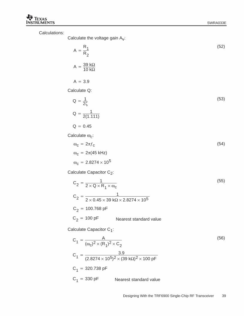
Calculations:Calculate the voltage gain Av:
A
R1R2
A 39 kΩ10 kΩ
A 3.9
Calculate Q:
Q 12ζ
Q 1
2(1.111)
Q 0.45
Calculate ωc:
ωc 2ƒc
ωc 2(45 kHz)
ωc 2.8274 × 10⁵
Calculate Capacitor C2:
Nearest standard value
C2 1
2 × Q × R1 × ωc
C2 1
2 × 0.45 × 39 kΩ × 2.8274 × 105
C2 100.768 pF
C2 100 pF
Calculate Capacitor C1:
Nearest standard value
C1 A
(ωc)2 × (R1)2 × C2
C1 3.9
(2.8274 × 10⁵)2 × (39 kΩ)2 × 100 pF
C1 320.738 pF
C1 330 pF
(52)
(53)
(54)
(55)
(56)

SWRA033E
40 Designing With the TRF6900 Single-Chip RF Transceiver
Check calculations: Calculate the cutoff frequency using standard values for components:
ƒc 1
2 R1 × R2 × C1 × C2
ƒc 1
2 39 kΩ × 10 kΩ × 330 pF × 100 pF
ƒc 44.364 kHz
Calculate Q using standard value for components:
Q
C1C2
× A
2A
Q
300 pF100 pF × 3.9
2(3.9)
Q 0.46
Calculate damping factor ζ using standard values for components:
Q 12ζ
Therefore,
ζ 1
2Q
ζ 1
2(0.46)
ζ 1.087
Figure 18 shows the output waveform of the low-pass filter amplifier/post-detection amplifier.The output of the amplifier is centered at 1.25 V, the reference voltage.
(57)
(58)
(59)

SWRA033E
41 Designing With the TRF6900 Single-Chip RF Transceiver
AMP_OUTTest PointVideo-Amplifier Output
Data-Slicer Input
1.25-V Reference
NOTE: Figure 17, the low-pass filter amplifier/post-detection amplifier schematic, has a connection to Vref as an input to the + terminalof the amplifier. Therefore, the low-pass filter amplifier/post-detection amplifier output is symmetrical about 1.25 V.
Figure 18. Low-Pass Filter Amplifier/Post-Detection Amplifier Output Waveform
3.8 Data Slicer [22]
The data slicer is a comparator circuit which outputs the necessary binary-logic levels forexternal CMOS circuitry. The output of the data slicer is the demodulated data at CMOS levels.
The block diagram shown in Figure 19 details the automatic-frequency-control (AFC) loop usedto determine the data slicer decision threshold.

SWRA033E
42 Designing With the TRF6900 Single-Chip RF Transceiver
_
+
R210 kΩ
32 31 30
C2
R1
C1
_
+
28DATA_OUT
RXDATATest Point
AMP_OUTTest Point
37VREFIntegrator
InternalVariableInductor
FM/FSKDemodulator
3435
External TankCircuit
39
Limiter
IF2_IN
Low-Pass Filter Amplifier/Post-Detection Amplifier
_
+
C
Vref ≈ 1.25 V
Vref
S&H_Cap29
Cterminal 29
Learn/Hold
Figure 19. AFC Control Loop Block Diagram
Figure 20 shows the input and output of the data slicer.
AMP_OUT Test PointLow-Pass Filter Amplifier/ Post-Detection AmplifierOutput and Data-Slicer Input.
RXDATATest PointData-Slicer Output
Figure 20. Data Output at AMP_OUT and RX_DATA Test Points
A typical input from the low-pass filter amplifier/post-detection amplifier to the data slicer isshown in the upper trace of Figure 20. The Amp_Out test point shown in Figure 19 issymmetrical at about 1.25 V (the reference voltage Vref of 1.25 V determines the decisionthreshold of the data slicer). The data slicer output measured at the RXDATA test point is shownin the lower trace of Figure 20. The amplitude of the waveform at the Amp_Out test point isdetermined by the gain of the low-pass filter amplifier/post-detection amplifier.

SWRA033E
43 Designing With the TRF6900 Single-Chip RF Transceiver
The integrator is an error amplifier which takes as an input the filtered output from the low-passfilter amplifier/post-detection amplifier. The integrator generates an error voltage proportional tothe difference between the frequency error of the external-tank circuit and the secondIF amplifier/limiter output signal. The error voltage output of the integrator adjusts the value ofthe internal variable inductor, providing a fine-tune adjustment to the external tank circuit.
The time constant of the AFC loop, used during learning mode, is calculated using the followingequation:
AFC 22 kΩ × Cterminal 29
The 22-kΩ resistor in equation (60) is internal to the TRF6900. The sample-and-hold (S&H)capacitor connected to terminal 29 is the only variable in equation (60) that can be used toadjust τAFC.
The AFC controls the resonant frequency of the external LC-tank circuit only in the learn mode.The AFC is open when the hold mode is selected. The S & H capacitor is charged during thelearn mode; this capacitor provides the dc-threshold offset voltage (offset from 1.25 V) to thedata slicer during the hold mode. An in-depth discussion of the learn and hold modes and theAFC loop is provided in the next section.
3.9 Learn and Hold Mode
The TRF6900 data slicer provides a binary-logic-level signal at the DATA_OUT terminal. Thissignal is derived from the demodulated and low-pass-filtered, received RF signal. A decisionthreshold for the data slicer, Vref, must be maintained to distinguish a received 1 from a received0 properly and to minimize any bit errors. This decision threshold is always set to 1.25 V,however, a dc offset is introduced to ensure a proper decision in the presence of anonconstant-dc bit sequence during receive.
As part of the AFC loop, the data slicer constantly integrates the incoming signal when in thelearn mode and charges external capacitor Cterminal 29 to an offset voltage from the dc voltagelevel Vref, which is proportional to the average demodulation dc-level. This dc voltage level (Vreftogether with the offset voltage) is used as the decision threshold. The offset voltage iscontrolled by the internal regulation loop and can be measured at terminal 29. While in the learnmode, Cterminal 29 determines the integration time constant τAFC of the entire AFC loop.
You can continually operate the TRF6900 receiver in learn mode if the TRF6900 is receiving aconstant dc (also called dc free) code such as Manchester, RZ, or biphase. However, a brieftraining or learning sequence is required at the beginning of each transmitted data packet toensure that the external capacitor on the receiver is charged to the correct dc threshold.
The training sequence must be constant-dc. Therefore, the use of alternating 1s and 0s isrecommended for this sequence. An alternating training sequence of 1s and 0s exhibits constantdc, independent of the data coding scheme used.
If the device is kept in learn mode and is receiving a nonconstant-dc code (such as NRZ) duringreception of valid data, the decision level is altered by long 1 or 0 sequences. Therefore, if anonconstant-dc data coding scheme is used, you must periodically switch between learn andhold modes.
While in hold mode, the internal regulation loop is open and an external dc offset can be appliedto terminal 29 to introduce an equivalent offset for proper 0 or 1 decisions.
(60)

SWRA033E
44 Designing With the TRF6900 Single-Chip RF Transceiver
When using nonconstant-dc codes, the unit is switched to the hold mode for reception of validdata after the training sequence. The data slicer stops integrating and uses the voltage Vref inconjunction with the offset voltage stored on Cterminal 29 as the decision threshold. Since thecharge on the external capacitor deteriorates, it must be periodically recharged to the averagedc level of the received data for proper data slicing. Thus, the unit must go back to learn mode,receive a training sequence to charge the external capacitor, set to hold mode, receive validdata, and so on.
The value of the external capacitor and the duration of the training sequence are governed byequations (60) and (61), respectively.
As a rule of thumb, the time constant τAFC (equal to 22 kΩ x Cterminal 29) of the AFC loop mustbe at least five times greater than the baseband modulating signal’s fundamental period Tfund.
5 × Tfund 22 kΩ × Cterminal 29
With Tfund known, equation (61) is solved for Cterminal 29
NOTES:
1. For nonconstant-dc codes:
For NRZ, the maximum fundamental frequency of the baseband modulating waveform, Ffund,is 1/2Tb => Tfund = 2Tb = To. The advantage of using nonconstant dc codes is that thesystem uses half the bandwidth to transmit the same data rate as compared to constant-dccodes. A disadvantage is that you need to switch between learn and hold modes on theTRF6900; that is, the TRF6900 device requires a periodic training sequence while in learnmode, followed by a switch to hold mode for reception of each data packet.
2. For constant-dc codes:
For Manchester, the maximum fundamental frequency of the baseband modulatingwaveform, Ffund, is 1/Tb => Tfund = Tb = To/2. The disadvantage of using constant-dc codesis that you need to use two times the bandwidth required with NRZ to get the same datarate. The advantage is that you do not need to switch between learn and hold modes on theTRF6900. You must initially account for the charge-up of Cterminal 29 when coming out ofstandby mode, and periodically redo the learning sequence at the beginning of each datapacket. However, you can keep the TRF6900 device in learn mode continuously.
3. Tb = 1/bit rateTo = 1/data rate = 2/bit rate2Tb = Todata rate = 1/To = 1/2Tb [Hz]bit rate = R = 1/Tb [bps](See Figure 25)
As a first approximation of the duration of the learning sequence, which includes a guard bandfor manufacturing tolerances and other factors, it is recommended to make the duration twotimes the minimum required.
Duration of training sequence = 2 × 5 × τAFC = 10 × τAFC
10 × 22 kΩ × Cterminal 29
(61)
(62)

SWRA033E
45 Designing With the TRF6900 Single-Chip RF Transceiver
For example:
(1) Nonconstant-dc coded data (NRZ):Bit rate = 10 kbps, Ffund = 5 kHz => Tfund = 200 µsBW required = BτAFC = 22 kΩ x Cterminal 295 x 200 µs = 1000 µs = 22 kΩ x Cterminal 29, solve for Cterminal 29:Cterminal 29 ≈ 46 nFFor a guard band, the alternating 1 and 0 learn sequence duration must be:10 × τAFC = 10 × 200 µs = 2 ms
(2) Constant dc coded data (Manchester, RZ, and biphase):Bit rate = 10 kbps, Ffund = 10 kHz => Tfund = 100 µsBW required = 2BτAFC = 22 kΩ x Cterminal 295 x 100 µs = 500 µs = 22 kΩ x Cterminal 29, solve for Cterminal 29:Cterminal 29 ≈ 23 nFFor a guard band, the alternating 1 and 0 learn sequence duration must be:10 × τAFC = 10 × 100 µs = 1 ms
These first approximations to the length of the learning sequence are a good starting point andmay be optimized (reduced) at a later time based on field test results.
Note that a very fast data rate can be used for the learning sequence, followed by a lower datarate for data transmission. This allows for a short learning sequence time in the receiver, atechnique patented by Texas Instruments. A slightly larger capacitor takes longer to charge(longer learning sequence duration), but the charge lasts longer and does not need to bere-learned as often. Conversely, a smaller capacitor takes a shorter time to charge (shorterlearning sequence), but the charge does not last long and must be relearned more often.
The external capacitor holds the charge used for the decision threshold for several seconds.However, the capacitor is discharged much faster if the device is set to standby mode, or if thedata slicer/demodulator is disabled.
The following sequence of events, in conjunction with Figure 21, can be used to better illustratethe use of the learning sequence and the learn and hold modes in a typical application:
1. Transmitter (TX) is transmitting a learning sequence of alternating 1s and 0s.
2. Receiver (RX) is put into active mode from standby mode: PLL, DDS, VCO, and DEMODall start to power up and activate. RX is also put into learning mode.
3. Cterminal 29 starts to charge up almost immediately.
4. TX continues to transmit a learning sequence.
5. After 600 µs (approximately 1 ms), the RX puts out data—not necessarily valid data. This1 ms is mostly a function of the start-up properties of the PLL, DDS, VCO, DEMOD, andthe integration time constant of the entire AFC loop. More learning sequences for a guardband, followed by a start preamble are needed.
6. Approximately 1 ms of additional learning sequence is used. Note that a portion of thetotal learning sequence duration needed, as per equation (62), is accounted for during the

SWRA033E
46 Designing With the TRF6900 Single-Chip RF Transceiver
initial RX start-up time. The remainder of the total time is needed to secure properreception and to give the microcontroller enough time to recognize the learning sequenceand look for a start preamble.
7. TX outputs a start preamble or a START bit.
8. RX receives a start preamble or START bit that TX produces, and determines thatlearning is over and data is to follow. RX switches to hold mode.
9. TX outputs data in NRZ format.
10. RX receives valid data in hold mode.
11. TX outputs a stop preamble at the end of the data packet.
12. After reception of the data packet and stop preamble, RX returns to standby mode.
13. After a predetermined time, RX starts to output a learning sequence and the receiver isreturned to active mode for reception. This sequence is repeated for the transmission andreception of each data packet.
7STOP
600 µsCapacitor at Terminal 29S&H Capacitor Charging
RX_DATA
C(Terminal 29)
STDBY
Figure 21. TRF6900 Wake-Up and Reception of Data
4 PCM-Data Coding Methods
Table 3. PCM Binary Coding Methods
PCM Code Type RZ NRZPhase
EncodedRef.
Level Transitions
Unipolar RZ X 0 levelChange of state from 0 to 1, and a1 at 1/2-bit period

SWRA033E
47 Designing With the TRF6900 Single-Chip RF Transceiver
Unipolar NRZ X 0 level Change of state from 0 to 1 or from 1 to 0
NRZ-L(Level)
XCenterof pulse
Change of state from 0 to 1 or from 1 to 0
NRZ-M(Mark)
XCenterof pulse
1 or mark is represented by change in level,0 or space is represented by no change in level
NRZ-S(Space)
XCenterof pulse
0 or space is represented by change in level,1 or mark is represented by no change in level
Bi-φ-Level,Manchester X
Centerof pulse
A 1 is represented by a 1/2-bit pulse at the start of the bit interval. A 0 isrepresented by a 1/2-bit pulse at the end of the bit interval.
Bi-φ-Mark(Mark) X
Centerof pulse
Transition occurs at the beginning of each bit interval.1 is represented by a second transition 1/2-bit later.0 is represented by no second transition 1/2-bit later.
Bi-φ-Space(Space) X
Centerof pulse
Transition occurs at the beginning of each bit interval.0 is represented by a second transition 1/2-bit later.1 is represented by no second transition 1/2-bit later.
Coding methods such as Unipolar RZ, Unipolar NRZ, NRZ-L, NRZ-M, and NRZ-S require alearn mode training sequence. During this training sequence (alternate 1s and 0s), the TRF6900receiver is operated in the learn mode. A switch to hold mode takes place after completion of thetraining sequence.
When continuous operation in the learn mode takes place using nonconstant dc codes such asUnipolar RZ, Unipolar NRZ, NRZ-L, NRZ-M, and NRZ-S, the decision level (that is, the dc level)is changed by the use of long 1 or 0 sequences.
The TRF6900 can be operated continuously in the learn mode when using constant dc codes orcodes that have no dc component, such as Manchester, split-phase, bipolar RZ, and RZ−AMIcodes. The RZ and split-phase codes assure at least one zero crossing per bit interval.However, the RZ and split-phase codes also require twice the transmission bandwidth of anNRZ code.
The split-phase codes are generated by multiplying an NRZ code by a square wave clockwaveform with a period equal to the bit duration Tb.
4.1 PCM Code Waveforms
The various PCM waveforms are illustrated in Figure 22 and described Table 3.

SWRA033E
48 Designing With the TRF6900 Single-Chip RF Transceiver
For the TRF6900+V = VCC − 0.7 V
−V = 0 V
1 01 10 10
Mark Space
Unipolar NRZ
+V
ReferenceLevel 0
ReferenceLevel 0
+V
−V
ReferenceLevel 0
+V
−V
ReferenceLevel 0
+V
−V
+V
ReferenceLevel 0
ReferenceLevel 0
+V
−V
ReferenceLevel 0
+V
−V
ReferenceLevel 0
+V
−V
Mark Mark Space Space Mark
Tb
PCM CodeUnipolar RZData Rate = 1/To (Hz)Bit Rate = 1/T b (bps)Tb = 1/Bit Rate RTo = 1/Data Rate = 2/Bit Rate RFundamental Frequency = 1/T b
Reference Level 0 is the Reference Point forZero Crossing if AC Coupled.The Data_Out Terminal on the TRF6900Provides Logic Levels Betweena −V of 0 V and a +V of V CC − 0.7 V.
Fundamental Frequency = 1/2T b
NRZ-L, Polar NRZ
NRZ-M
NRZ-(I)
NRZ-S
Split-Phase Level,Bi-∅-L, Manchester
To
Split-Phase Mark,Bi-∅-M
Split-Phase Space,Bi-∅-S
Figure 22. Pulse-Code-Modulation (PCM) Waveforms
5 Image Response
The use of a low IF frequency in the US ISM band (902 to 928 MHz) requires the proper system-architecture design. With the use of a 10.7-MHz IF, the image band and required LO band fallwithin the desired RF input band, as shown in Figure 23. Image noise from the receiver antenna,device LNA, and mixer-driver amplifiers may have an adverse effect on receiver sensitivity.
With a portion of the required LO in the desired input band, the LO phase noise, and the LOharmonics can remix in the mixer and cause further degradation of the receiver sensitivity.
With a 10.7-MHz IF, the image response of the mixer is 21.4 MHz away from the received signal.Due to the 26-MHz width of the ISM band, the image frequency is in-band for some portion ofthe band and cannot be filtered out with a fixed preselector filter.

SWRA033E
49 Designing With the TRF6900 Single-Chip RF Transceiver
Proper system architecture includes using only a portion of the ISM band and using apreselector filter that covers only the sub-band in use. In addition, it is important to ensure thatthe power of the desired signal is higher than any potential interferer when maximizing systemsensitivity.
IFRF
LO
10.7 MHz902 to 928 MHz
891.3 to 917.3 MHz
902 MHz 928 MHz
891.3 MHz 917.3 MHz
880.6 MHz 906.6 MHz
Real
LO
Image
Real = RF −LOImage = LO −RF
Figure 23. USA ISM Band Real vs Image Frequencies
6 Determination of Signal-to-Noise RatioThe voltage level at the output of the low-pass filter amplifier/post-detection amplifier is theoutput signal-to-noise ratio (S/N). The output signal-to-noise ratio is usually expressed indecibels (dB). Equation (63) demonstrates how to determine the output S/N.
SN CN MNI dB
Where:S/N: Output signal-to-noise ratio, in dBC/N: Input to the receiver carrier-to-noise ratio, in dBMNI: Modulation-noise-improvement factor, in dB
The carrier-to-noise ratio (C/N) is the level of the input to the limiter stage. The carrier-to-noiseratio is calculated using equation (64).
CN 174 dB NF 10 log BWIF RF Input Level (dB)
Where:–174 dB: Thermal noise floorNF: Cascaded noise figure of the receiver system determined by the Friis
equation [see equation (65)]BWIF: IF filter bandwidthRF Input Level: Minimum input signal level to the receiver (dB)
NF NF1
NF2 1
Gain1
NF3 1
Gain2 Gain1
NF4 1
Gain3 Gain2 Gain1
Where:NFn = 10NFn(dB)/10
Gainn = 10Gainn(dB)/10
(63)
(64)
(65)

SWRA033E
50 Designing With the TRF6900 Single-Chip RF Transceiver
MNI 3 m2
BWIF2 b
MNIdB 10 log MNI
Where:MNI: Modulation-noise-improvement factor.m = ∆ƒ/b: Modulation index∆ƒ: Peak frequency deviation of the received signalBWIF: IF filter bandwidthb: Bandwidth of the low-pass filter amplifier/post-detection
amplifier. Bandwidth b is set to two times the data rate.
7 PCB-Board Layout Guidelines [20]
TI suggests the following layout guidelines to attain the most robust and functional PCB layout:
• The power amplifier output inductor must be placed as close as possible to the TRF6900 IC.
• The power amplifier, LNA, PLL, DDS, and demodulator VCC bypass capacitors must beplaced as close as possible to the TRF6900 IC.
• The VCO tank inductor must be placed as close as possible to the TRF6900 IC.
• The VCO tank capacitors must be placed as close as possible the VCO tank inductor. Thetraces from the VCO inductor to the VCO capacitors must be symmetrical.
• The LNA input-matching inductor must be placed as close as possible to the TRF6900 IC.
• The LNA matching-circuit components must be placed as close together as possible.
• The PLL loop filter traces must be kept as short as possible, and the ground plane must beused to isolate the PLL loop filter from the power amplifier output.
• The demodulation tank circuit inductor must be placed as close as possible to the TRF6900IC.
• The demodulation tank circuit capacitors must be placed as close as possible to thedemodulation tank inductor.
• Good grounding practices must be followed in the VCO, power amplifier, LNA input andoutput, IF, and crystal circuit areas.
• The PCB must ideally have one layer as a reference-ground plane. Any critical ground areason the component side of the PCB should be connected by vias to this ground plane.
• The edges of the PCB board must be part of the ground plane.
• RF and digital grounds may be kept separate and tied at a common point.
• Ground vias must be spaced by a maximum of 1/4 wavelength of the highest frequencyused. Closer spacing of the vias is recommended.
7.1 Clock-Circuit PCB-Layout Considerations
Layout considerations for the clock oscillator include:
(66)
(67)
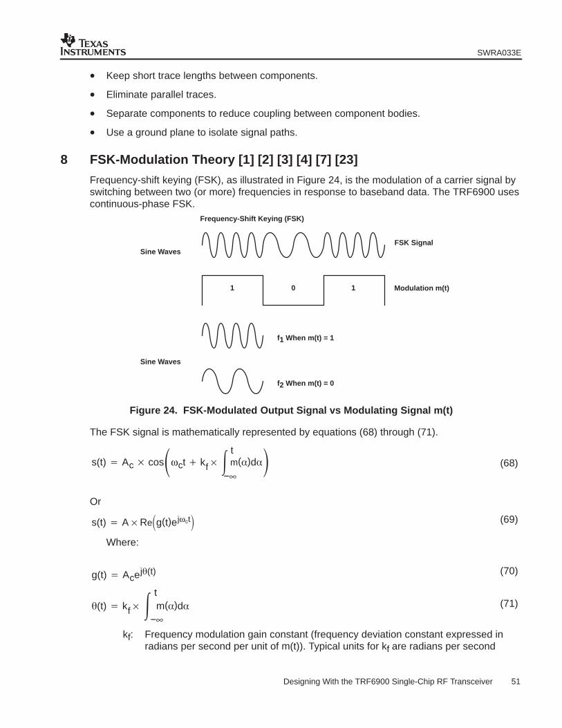
SWRA033E
51 Designing With the TRF6900 Single-Chip RF Transceiver
• Keep short trace lengths between components.
• Eliminate parallel traces.
• Separate components to reduce coupling between component bodies.
• Use a ground plane to isolate signal paths.
8 FSK-Modulation Theory [1] [2] [3] [4] [7] [23]
Frequency-shift keying (FSK), as illustrated in Figure 24, is the modulation of a carrier signal byswitching between two (or more) frequencies in response to baseband data. The TRF6900 usescontinuous-phase FSK.
Modulation m(t)
FSK Signal
1 0 1
Frequency-Shift Keying (FSK)
f1 When m(t) = 1
f2 When m(t) = 0
Sine Waves
Sine Waves
Figure 24. FSK-Modulated Output Signal vs Modulating Signal m(t)
The FSK signal is mathematically represented by equations (68) through (71).
s(t) Ac cosωct kf × m()dt
−∞
Or
s(t) A × Reg(t)ejωct
Where:
g(t) Acej(t)
(t) kf × m()dt
−∞kf: Frequency modulation gain constant (frequency deviation constant expressed in
radians per second per unit of m(t)). Typical units for kf are radians per second
(68)
(69)
(70)
(71)

SWRA033E
52 Designing With the TRF6900 Single-Chip RF Transceiver
per volt.kf: Equal to 2πƒd, where ƒd is the deviation constant in hertz per unit of m(t).α: Integration dummy variableθ(t): Phase waveform
The baseband signal is represented by m(t). This signal is discontinuous at switching time, butthe phase function θ(t) is continuous, since it is proportional to the integral of m(t). If the data-input waveform is binary, the resulting FSK waveform is called binary FSK (BFSK).
Frequency-shift keying is a form of frequency modulation (FM). Frequency modulation is, in turn,a form of angle modulation. Therefore, the equations and theory that apply to FM modulationcan be applied to FSK modulation. FM modulation requires that the time derivative of the phaseof the carrier signal be varied linearly with the message signal m(t). The instantaneousfrequency ωi is defined in equations (72) through (74).
ωi(t) didt
it c
ddt
ddt
kf m(t)
Where the function ddt
is the frequency deviation.
These equations show that the frequency deviation of the carrier is proportional to themodulating signal.
The output of the FM modulator is shown in equation (75).
s(t) Ac cosωct kf × m()dt
−∞
Substituting kf = 2πƒd into equation (75) yields:
s(t) Ac cosωct 2ƒd × m()dt
−∞
The frequency deviation of the FM modulator is proportional to m(t). The instantaneousfrequency of the FM modulator output is maximum when m(t) is maximum, and minimum whenm(t) is minimum. Let m(t) = a cos ωmt, and substitute this value in equations (73) and (74).
ωi ωc a kf cos ωmt
With ∆ω = a kf, then
ωi ωc ω cos ωmt
The peak-frequency-deviation constant is defined as ∆ω.Note: ∆ω/2π = ƒd = ∆ƒ, and ωm/2π = ƒm
The phase of the FM signal can then be defined as
(72)
(73)
(74)
(75)
(76)
(77)
(78)

SWRA033E
53 Designing With the TRF6900 Single-Chip RF Transceiver
(t) ωct ωωm sin ωmt
or
(t) ωct sin ωmt
Where β is the modulation index
ωωm
ƒƒm
The modulation index β is only defined for sinusoidal modulation. When an arbitrary m(t) is used,the accepted expression for bandwidth uses the deviation ratio D.
D is defined as: D peak frequency deviation
Bandwidth of m(t) ; D (ƒƒm), where ƒm is the bandwidth of m(t)
The deviation ratio D performs the same function for nonsinusoidal modulation as themodulation index β performs for sinusoidal modulation.
If β < 0.2, the modulation is narrowband frequency modulation (NBFM). If β > 0.2, then themodulation is wideband frequency modulation (WBFM). For FSK, in most cases, the modulationis WBFM. The transmission bandwidth required for WBFM and/or FSK is determined byCarson’s rule, equation (84).
You can define the modulation index and observe the FSK spectrum as the modulation index isvaried. The frequency modulation index is defined in equation (82).
Frequency modulation index ƒB
This index is for FM modulation with sinusoidal modulation, where ∆f is the peak-frequencydeviation and B is the bandwidth of the modulating signal. An alternate definition of themodulation index is sometimes used with digital signals—the digital modulation index, which isdenoted by h.
Digital modulation index h ƒ × To 2ƒR
Where:R = 1/Tb = 2/To: Bit rate [bps]Tb: Time interval for one bitTo: Period of the data modulation = 1/data rate [Hz]
m(t)
0
t
Baseband Modulating Signal
Logic 1
Logic 0
Tb
To
1
Figure 25. Input-Data Signal
(79)
(80)
(81)
(82)
(83)

SWRA033E
54 Designing With the TRF6900 Single-Chip RF Transceiver
Figure 25 illustrates the relationship between Tb and To. Figure 26 illustrates the FSK spectra asthe modulation index h is varied from 0.5 to more than 1.5.
Depending on the modulation index of the signal, an FSK spectrum can appear (withpseudorandom data) anywhere between a single peak at the carrier and two peaks separatedfrom the carrier. The separation of the peaks is not necessarily the frequency deviation. Thedistance between the peaks is a function of both the modulation index h and the frequencydeviation.
When non-pseudorandom data is used, the output spectrum appears as two SINC functions thatare composed of impulses. A non-pseudorandom data stream is an alternating 1,0,1,0,1,0…pattern. When the modulation index is varied, the two SINC functions get closer together ormove further apart. When the modulation index h is increased from 0.5 to 1.0, the spectrumconcentrates about ƒ1 and ƒ2. When the modulation index is increased beyond 2, the spectrumstarts to spread out and the amplitude level decreases.
The modulation index h must be between 0.5 and 1 or 2 maximum to conserve bandwidth andminimize BER. Table 4 summarizes the modulation index information.
1
0 0.5 1 1.5−0.5−1−1.5ω ωo
ωb
h = 0.5 MSK
h = 1.25
h = 0.7
h = 1.6
0.8
0.6
0.4
0.2
Figure 26. Power Spectral Density of FSK for Pseudorandom Data

SWRA033E
55 Designing With the TRF6900 Single-Chip RF Transceiver
Table 4. Modulation Index h vs Power Spectra
Modulation Index h Power Spectra Effects
h < 0.5 FSK signals are less orthogonal and BER increases (do not use).
h = 0.5 Minimum shift keying. MSK equals the narrowest spectrum for orthogonality.
h 0.6 Spectrum is smooth and single-peaked at carrier frequency.
0.6 < h < 1.0 Spectrum is smooth and well confined; spectrum moves form single-peak at carrier frequency to peaksat M frequencies (as h -> 1, spectra begins to peak at M frequencies).
h = 1.0 Impulses occur at M frequencies.
h > 1.0 Spectrum is broadest, peaks outside carrier frequency ± bit rate/2, decreases in sharpness andamplitude.
9 Required Bandwidth for Transmit and Receive
The approximate bandwidth BT for an FSK signal is given by Carson’s rule shown inequation (84).
BT 2( 1)B
Where:β: Modulation index hB: Bandwidth of the modulation waveform, m(t); B = 1/To
When rectangular pulses are used (B = R), Carson’s rule is stated as:
BT 2(ƒ R)
Where:BT: Transmission bandwidth for the FSK signal∆ƒ : Peak frequency deviationR: Bit rate
For wideband FSK (WBFSK) where β > 1, ∆ƒ is the dominant term and equation (85) can bereduced to:
BT ≅ 2∆ƒ for WBFSK
For narrowband FSK (NBFSK), where β < 0.2, the transmission bandwidth is found as:
BT ≅ 2B ≅ 2R for NBFSK
The bandwidth determined by equation (85) is generous and can be considered as themaximum bandwidth required. The minimum bandwidth required is bounded by:
BT ≅ 2∆ƒ for WBFSK.
Note: A periodic random data requires less bandwidth than periodic data.
Example 4.
Given an FSK system with the following parameters:
ƒd = ∆ƒ = 10-kHz peak deviation (20-kHz peak-to-peak frequency deviation)
Bit rate R 1
Tb 10 kbps
(84)
(85)
(86)
(87)
(88)
(89)

SWRA033E
56 Designing With the TRF6900 Single-Chip RF Transceiver
Bit duration = 1/10 kbps
Determine:
1. Digital modulation index h
2. Required bandwidth
Solution:
1. Digital modulation index h
Digital modulation index h ƒ × To 2ƒR
Digital modulation index h 10 kHz × 200 µs 2(10 kHz)
10 kHz 2
2. Required bandwidth
Carson’s rule is stated as:
BT 2(ƒ R)
Where:BT: Transmission bandwidth for the FSK signal∆ƒ : Peak frequency deviationR: Bit rate
BT 2(10 kHz 10 kHz)
BT 40 kHz
As a lower bound for WBFSK,
BT ≅ 2∆ƒ ≅ 2(10 kHz) ≅ 20 kHz
Therefore, a minimum bandwidth of 20 kHz is required for this system, with a maximumbandwidth of 40 kHz as the upper bound.
10 Bit Error Rate
For noncoherent FSK modulation the bit error rate (BER) is defined in equation (93).
Pe 12
e
12
× EbNo
Where:Pe: Bit error rate for FSK modulationEb/No: Signal-to-noise ratio
EbNO
SN 10 log ENBR
Where:S/N: Signal-to-noise ratio expressed in dB
(90)
(91)
(92)
(93)
(94)

SWRA033E
57 Designing With the TRF6900 Single-Chip RF Transceiver
ENB: Effective noise bandwidth, equal to the bandwidth of the IFfilter used in the FSK receiver system
R: Bit rate of 1/Tb
Note: The S/N used in equation (94) is the signal-to-noise ratio measured at the input tothe limiter stage. This is the carrier-to-noise ratio C/N calculated by equation (64).

SWRA033E
58 Designing With the TRF6900 Single-Chip RF Transceiver
11 References1. Loy, Matt, Understanding and Enhancing Sensitivity in Receivers for Wireless Applications,
Texas Instruments application note SWRA030, May 1999
2. Zeimer, R.E., Tranter, W.H., Principles of Communications Systems, Modulation, and Noise, 4th
Ed., John Wiley and Sons, 1995
3. Stremler, Ferrel G., Introduction to Communication Systems 3rd Ed., Addison-Wesley, 1992
4. Couch, Leon W., Digital and Analog Communication Systems 5th Ed., Prentice-Hall, 1997
5. Erst, Steven J., Electronic Equations Handbook, Tab Division of McGraw-Hill, 1989
6. Rappaport, Theodore S., Wireless Communications Principles and Practice, Prentice-Hall,1996
7. Kaufman, Milton, Seidman, Arthur H., Handbook of Electronics Calculations, McGraw-Hill, 1979
8. Franceschino, Albert, An IF Communication Circuit Tutorial, Motorola application note, AN1539,1996
9. Sofianos, Paul, Practical Solutions for Medium Data Rate Wireless Communications, Motorolaapplication note, AN1691, 1999
10. Erst, Steven J., Receiver Systems Design, Artech House, 1984
11. Hsu, Hwei, Schaum’s Outline Theory and Problems Analog and Digital Communications,McGraw-Hill, 1993
12. Razavi, Behzad, RF Microelectronics, Prentice Hall, 1998
13. Rohde, Ulrich L, Whitaker, Jerry C, Bucher, TTN, Communications Receivers: Principles andDesign, 2nd Ed., McGraw-Hill, 1996
14. Krauss, Herbert L., Bostian, Charles W., Raab, Frederick H., Solid State Radio Engineering,John Wiley and Sons, 1980
15. Hayward, Wes, Introduction to Radio Frequency Design, American Radio Relay League(ARRL), 1994
16. Dao, A., Integrated LNA and Mixer Basics, National Semiconductor application note, AN-884,1995
17. Meador, Don A., Laplace Circuit Analysis and Active Filters, Prentice Hall, 1991
18. Trofimenkoff, F.N., Treleaven, David H., Bruton, L.T., Noise Performance of RC-Active QuadraticFilter Sections, IEEE Trans. Circuits Theory, vol. CT-20, pp. 524-532, Sept.1973
19. Sklar, Bernard, Digital Communications Fundamentals and Applications, Prentice-Hall, Inc.1988
20. Johnson, Howard, Graham, Martin, High Speed Digital Design: A Handbook of Black Magic,Prentice Hall, Inc. 1993
21. Analog Devices: Technical Tutorial on Digital Signal Synthesis, Analog Devices, 1999.
22. TRF6900A Single-Chip RF Transceiver, Texas Instruments data sheet SLAS258, May 2001.
23. Peebles, Peyton Z. Jr., Digital Communication Systems, Prentice-Hall, 1987.
24. Rohde, Ulrich L., Microwave and Wireless Synthesizers: Theory and Design, John Wiley andSons, 1997.

IMPORTANT NOTICE
Texas Instruments Incorporated and its subsidiaries (TI) reserve the right to make corrections, modifications,enhancements, improvements, and other changes to its products and services at any time and to discontinueany product or service without notice. Customers should obtain the latest relevant information before placingorders and should verify that such information is current and complete. All products are sold subject to TI’s termsand conditions of sale supplied at the time of order acknowledgment.
TI warrants performance of its hardware products to the specifications applicable at the time of sale inaccordance with TI’s standard warranty. Testing and other quality control techniques are used to the extent TIdeems necessary to support this warranty. Except where mandated by government requirements, testing of allparameters of each product is not necessarily performed.
TI assumes no liability for applications assistance or customer product design. Customers are responsible fortheir products and applications using TI components. To minimize the risks associated with customer productsand applications, customers should provide adequate design and operating safeguards.
TI does not warrant or represent that any license, either express or implied, is granted under any TI patent right,copyright, mask work right, or other TI intellectual property right relating to any combination, machine, or processin which TI products or services are used. Information published by TI regarding third-party products or servicesdoes not constitute a license from TI to use such products or services or a warranty or endorsement thereof.Use of such information may require a license from a third party under the patents or other intellectual propertyof the third party, or a license from TI under the patents or other intellectual property of TI.
Reproduction of information in TI data books or data sheets is permissible only if reproduction is withoutalteration and is accompanied by all associated warranties, conditions, limitations, and notices. Reproductionof this information with alteration is an unfair and deceptive business practice. TI is not responsible or liable forsuch altered documentation.
Resale of TI products or services with statements different from or beyond the parameters stated by TI for thatproduct or service voids all express and any implied warranties for the associated TI product or service andis an unfair and deceptive business practice. TI is not responsible or liable for any such statements.
Following are URLs where you can obtain information on other Texas Instruments products and applicationsolutions:
Products Applications
Amplifiers amplifier.ti.com Audio www.ti.com/audio
Data Converters dataconverter.ti.com Automotive www.ti.com/automotive
DSP dsp.ti.com Broadband www.ti.com/broadband
Interface interface.ti.com Digital Control www.ti.com/digitalcontrol
Logic logic.ti.com Military www.ti.com/military
Power Mgmt power.ti.com Optical Networking www.ti.com/opticalnetwork
Microcontrollers microcontroller.ti.com Security www.ti.com/security
Telephony www.ti.com/telephony
Video & Imaging www.ti.com/video
Wireless www.ti.com/wireless
Mailing Address: Texas Instruments
Post Office Box 655303 Dallas, Texas 75265
Copyright 2005, Texas Instruments Incorporated