Embed Size (px)
Citation preview

PRODUCT SPECIFICATION
Nordic Semiconductor ASA - Vestre Rosten 81, N-7075 Tiller, Norway - Phone +4772898900 - Fax +4772898989 Revision: 1.0 Page 1 of 38 December 2004
Single chip 2.4 GHz Transceiver
FEATURES
APPLICATIONS
• True single chip GFSK transceiver in a small 24-pin package (QFN24 5x5mm)
• Wireless mouse, keyboard, joystick • Keyless entry
• Data rate 0 to1Mbps • Wireless data communication • Only 2 external components • Alarm and security systems
• Multi channel operation • 125 channels • Channel switching time <200µs. • Support frequency hopping
• Home automation • Surveillance • Automotive
• Data slicer / clock recovery of data • Telemetry • Address and CRC computation • Intelligent sports equipment • DuoCeiver™ for simultaneous dual receiver
topology • ShockBurst™ mode for ultra-low power
operation and relaxed MCU performance
• Industrial sensors • Toys
• Power supply range: 1.9 to 3.6 V • Low supply current (TX), typical 10.5mA peak
@ -5dBm output power • Low supply current (RX), typical 18mA peak in
receive mode
• 100 % RF tested
• No need for external SAW filter
• World wide use
GENERAL DESCRIPTION nRF2401A is a single-chip radio transceiver for the world wide 2.4 - 2.5 GHz ISM band. The transceiver consists of a fully integrated frequency synthesizer, a power amplifier, a crystal oscillator and a modulator. Output power and frequency channels are easily programmable by use of the 3-wire serial interface. Current consumption is very low, only 10.5mA at an output power of -5dBm and 18mA in receive mode. Built-in Power Down modes makes power saving easily realizable.
QUICK REFERENCE DATA Parameter Value Unit
Minimum supply voltage 1.9 V Maximum output power 0 dBm Maximum data rate 1000 kbps Supply current in transmit @ -5dBm output power 10.5 mA Supply current in receive mode 18 mA Temperature range -40 to +85 °C Sensitivity -93 dBm Supply current in Power Down mode 400 nA
Table 1 nRF2401A quick reference data
nRF2401A
PRODUCT SPECIFICATION nRF2401A Single Chip 2.4 GHz Radio Transceiver
Nordic Semiconductor ASA - Vestre Rosten 81, N-7075 Tiller, Norway - Phone +4772898900 - Fax +4772898989 Revision: 1.0 Page 2 of 38 December 2004
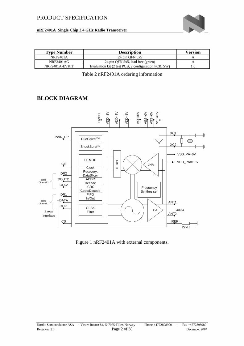
Type Number Description Version NRF2401A 24 pin QFN 5x5 A
NRF2401AG 24 pin QFN 5x5, lead free (green) A NRF2401A-EVKIT Evaluation kit (2 test PCB, 2 configuration PCB, SW) 1.0
Table 2 nRF2401A ordering information
BLOCK DIAGRAM
DV
DD
VD
D=3
V
VD
D=3
V
XC1
XC2
400Ω
IREF
VDD_PA=1.8V
VSS_PA=0V
ANT1
ANT2
22kΩ
VS
S=0
V
VS
S=0
V
VD
D=3
V
VS
S=0
V
VS
S=0
V
FrequencySynthesiser
PA
LNA
IF B
PFDEMOD
ClockRecovery,DataSlicer
ADDRDecode
FIFOIn/Out
CRCCode/Decode
DuoCeiverTM
ShockBurstTM
GFSKFilter
DATA
CS
CLK1
3-wireinterface
PWR_UP
CE
CLK2
DOUT2
DR2
DR1
DataChannel 2
DataChannel 1
Figure 1 nRF2401A with external components.

PRODUCT SPECIFICATION nRF2401A Single Chip 2.4 GHz Radio Transceiver
Nordic Semiconductor ASA - Vestre Rosten 81, N-7075 Tiller, Norway - Phone +4772898900 - Fax +4772898989 Revision: 1.0 Page 3 of 38 December 2004
PIN FUNCTIONS Pin Name Pin function Description
1 CE Digital Input Chip Enable Activates RX or TX mode 2 DR2 Digital Output RX Data Ready at Data Channel 2 (ShockBurst™ only) 3 CLK2 Digital I/O Clock Output/Input for RX Data Channel 2 4 DOUT2 Digital Output RX Data Channel 2 5 CS Digital Input Chip Select Activates Configuration Mode 6 DR1 Digital Output RX Data Ready at Data Channel 1 (ShockBurst™ only) 7 CLK1 Digital I/O Clock Input (TX) & Output/Input (RX) for Data Channel 1
3-wire interface 8 DATA Digital I/O RX Data Channel 1/TX Data Input/ 3-wire interface 9 DVDD Power Output Positive Digital Supply output for de-coupling purposes 10 VSS Power Ground (0V) 11 XC2 Analog Output Crystal Pin 2 12 XC1 Analog Input Crystal Pin 1 13 VDD_PA Power Output Power Supply (+1.8V) to Power Amplifier 14 ANT1 RF Antenna interface 1 15 ANT2 RF Antenna interface 2 16 VSS_PA Power Ground (0V) 17 VDD Power Power Supply (+3V DC) 18 VSS Power Ground (0V) 19 IREF Analog Input Reference current 20 VSS Power Ground (0V) 21 VDD Power Power Supply (+3V DC) 22 VSS Power Ground (0V) 23 PWR_UP Digital Input Power Up 24 VDD Power Power Supply (+3V DC)
Table 3 nRF2401A pin function
PIN ASSIGNMENT
VDD
DATA
nRF2401A
QFN24 5x5
DVDD
VDD
PWR_UP
VSS
ANT2
VSS
VSS_PA
CLK1
CE
23 22 2124
987
4
3
2
1 18
17
16
6
5
VDD_PA
ANT114
IREFVSS
20 19
11 12
13
15
10
CS
XC2 XC1
DR1
DR2
CLK2
VDD VSS
Figure 2 nRF2401A pin assignment (top view) for a QFN24 5x5 package.

PRODUCT SPECIFICATION nRF2401A Single Chip 2.4 GHz Radio Transceiver
Nordic Semiconductor ASA - Vestre Rosten 81, N-7075 Tiller, Norway - Phone +4772898900 - Fax +4772898989 Revision: 1.0 Page 4 of 38 December 2004
ELECTRICAL SPECIFICATIONS
Conditions: VDD = +3V, VSS = 0V, TA = - 40ºC to + 85ºC Symbol Parameter (condition) Notes Min. Typ. Max. Units
Operating conditions VDD Supply voltage 1.9 3.0 3.6 V
TEMP Operating Temperature -40 +27 +85 ºC
Digital input pin VIH HIGH level input voltage VDD- 0.3 VDD V VIL LOW level input voltage Vss 0.3 V
Digital output pin
VOH HIGH level output voltage (IOH=-0.5mA) VDD- 0.3 VDD V VOL LOW level output voltage (IOL=0.5mA) Vss 0.3 V
General RF conditions fOP Operating frequency 1) 2400 2524 MHz
fXTAL Crystal frequency 2) 4 20 MHz ∆f Frequency deviation ±156 kHz
RGFSK Data rate ShockBurst™ >0 1000 kbps RGFSK Data rate Direct Mode 3) 250 1000 kbps
FCHANNEL Channel spacing 1 MHz
Transmitter operation PRF Maximum Output Power 4) 0 +4 dBm PRFC RF Power Control Range 16 20 dB PRFCR RF Power Control Range Resolution ±3 dB PBW 20dB Bandwidth for Modulated Carrier 1000 kHz PRF2 2nd Adjacent Channel Transmit Power 2MHz -20 dBm PRF3 3rd Adjacent Channel Transmit Power 3MHz -40 dBm IVDD Supply current @ 0dBm output power 5) 13 mA IVDD Supply current @ -20dBm output power 5) 8.8 mA IVDD Average Supply current @ -5dBm output
power, ShockBurst™ 6) 0.8 mA
IVDD Average Supply current in stand-by mode 7) 12 µA IVDD Average Supply current in power down 400 nA
Receiver operation IVDD Supply current one channel 250kbps 18 mA IVDD Supply current one channel 1000kbps 19 mA IVDD Supply current two channels 250kbps 23 mA IVDD Supply current two channels 1000kbps 25 mA
RXSENS Sensitivity at 0.1%BER (@250kbps) -93 dBm RXSENS Sensitivity at 0.1%BER (@1000kbps) -85 dBm C/ICO C/I Co-channel 8) 10/4 dB C/I1ST 1st Adjacent Channel Selectivity C/I 1MHz 8) -20/0 dB C/I2ND 2nd Adjacent Channel Selectivity C/I 2MHz 8) -37/-20 dB C/I3RD 3rd Adjacent Channel Selectivity C/I 3MHz 8) -43/-30 dB RXB Blocking Data Channel 2 -45/-41 dB
1) Usable band is determined by local regulations 2) The crystal frequency may be chosen from 5 different values (4, 8, 12, 16, and 20MHz) which are specified in the
configuration word, see Table 8. 16MHz are required for 1Mbps operation. 3) Data rate must be either 250kbps or 1000kbps. 4) Antenna load impedance = 100Ω+j175Ω 5) Antenna load impedance = 100Ω+j175Ω. Effective data rate 250kbps or 1Mbps. 6) Antenna load impedance = 100Ω+j175Ω. Effective data rate 10kbps. 7) Current if 4 MHz crystal is used. 8) 250kbps/1000kbps.
Table 4 nRF2401A RF specifications

PRODUCT SPECIFICATION nRF2401A Single Chip 2.4 GHz Radio Transceiver
Nordic Semiconductor ASA - Vestre Rosten 81, N-7075 Tiller, Norway - Phone +4772898900 - Fax +4772898989 Revision: 1.0 Page 5 of 38 December 2004
PACKAGE OUTLINE nRF2401AG uses the GREEN QFN24 5x5 package, with matt tin plating. nRF2401A uses the QFN24 5x5 package, with SnPb plating. Dimensions are in mm.
Package Type A A1 A2 b D/E D1/E1 e J K L R Punch QFN24
(5x5 mm) Min typ. Max
0.8
0.9
0.0 0.02 0.05
0.65
0.69
0.25 0.3
0.35
5 BSC
4.75 BSC
0.65 BSC
3.47 3.57 3.67
3.47 3.57 3.67
0.3 0.4 0.5
1.235 1.335 1.435
Figure 3 nRF2401AG GREEN Package outline.

PRODUCT SPECIFICATION nRF2401A Single Chip 2.4 GHz Radio Transceiver
Nordic Semiconductor ASA - Vestre Rosten 81, N-7075 Tiller, Norway - Phone +4772898900 - Fax +4772898989 Revision: 1.0 Page 6 of 38 December 2004
Absolute Maximum Ratings
Supply voltages VDD............................ - 0.3V to + 3.6V VSS .................................................. 0V Input voltage VI....................... - 0.3V to VDD + 0.3V Output voltage VO...................... - 0.3V to VDD + 0.3V
Total Power Dissipation PD (TA=85°C) ............................. 90mW Temperatures Operating Temperature…. - 40°C to + 85°C Storage Temperature….… - 40°C to + 125°C Note: Stress exceeding one or more of the limiting values may cause permanent damage to the device.
ATTENTION! Electrostatic Sensitive Device Observe Precaution for handling.
PRODUCT SPECIFICATION nRF2401A Single Chip 2.4 GHz Radio Transceiver
Nordic Semiconductor ASA - Vestre Rosten 81, N-7075 Tiller, Norway - Phone +4772898900 - Fax +4772898989 Revision: 1.0 Page 7 of 38 December 2004
Glossary of Terms
Term Description CLK Clock CRC Cyclic Redundancy Check CS Chip Select CE Chip Enable DR Data Ready GFSK Gaussian Frequency Shift Keying ISM Industrial-Scientific-Medical MCU Micro controller OD Overdrive PWR_DWN Power Down PWR_UP Power Up RX Receive ST_BY Standby TX Transmit
Table 5 Glossary
PRODUCT SPECIFICATION nRF2401A Single Chip 2.4 GHz Radio Transceiver
Nordic Semiconductor ASA - Vestre Rosten 81, N-7075 Tiller, Norway - Phone +4772898900 - Fax +4772898989 Revision: 1.0 Page 8 of 38 December 2004
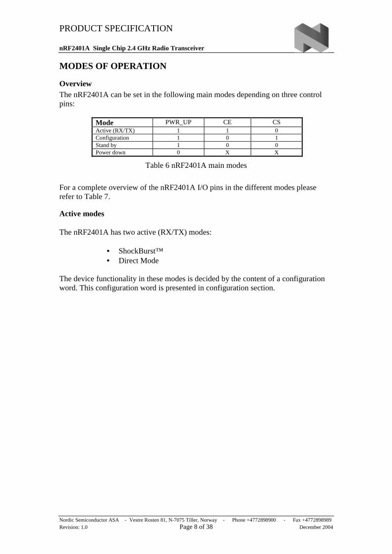
MODES OF OPERATION
Overview The nRF2401A can be set in the following main modes depending on three control pins:
Mode PWR_UP CE CS Active (RX/TX) 1 1 0 Configuration 1 0 1 Stand by 1 0 0 Power down 0 X X
Table 6 nRF2401A main modes
For a complete overview of the nRF2401A I/O pins in the different modes please refer to Table 7.
Active modes The nRF2401A has two active (RX/TX) modes:
• ShockBurst™ • Direct Mode
The device functionality in these modes is decided by the content of a configuration word. This configuration word is presented in configuration section.

PRODUCT SPECIFICATION nRF2401A Single Chip 2.4 GHz Radio Transceiver
Nordic Semiconductor ASA - Vestre Rosten 81, N-7075 Tiller, Norway - Phone +4772898900 - Fax +4772898989 Revision: 1.0 Page 9 of 38 December 2004
ShockBurst™ The ShockBurst™ technology uses on-chip FIFO to clock in data at a low data rate and transmit at a very high rate thus enabling extremely power reduction. When operating the nRF2401A in ShockBurst™, you gain access to the high data rates (1 Mbps) offered by the 2.4 GHz band without the need of a costly, high-speed micro controller (MCU) for data processing. By putting all high speed signal processing related to RF protocol on-chip, the nRF2401A offers the following benefits: • Highly reduced current consumption • Lower system cost (facilitates use of less expensive micro controller) • Greatly reduced risk of ‘on-air’ collisions due to short transmission time The nRF2401A can be programmed using a simple 3-wire interface where the data rate is decided by the speed of the micro controller. By allowing the digital part of the application to run at low speed while maximizing the data rate on the RF link, the nRF ShockBurst™ mode reduces the average current consumption in applications considerably. ShockBurst™ principle When the nRF2401A is configured in ShockBurst™, TX or RX operation is conducted in the following way (10 kbps for the example only).
8-bitMCU
nRF2401AContinuous 10kbps
1MbpsShockBurstTMFIFO
Figure 4 Clocking in data with MCU and sending with ShockBurst technology
Time mS0 20 40 60 80 100 120 140 160 180 200 220 240
10mA periode
10mA period
Without ShockBurstTM, running at speed dictated by 10Kbs MCU
10Kbs MCU with ShockBurstTM
Figure 5 Current consumption with & without ShockBurst technology
PRODUCT SPECIFICATION nRF2401A Single Chip 2.4 GHz Radio Transceiver
Nordic Semiconductor ASA - Vestre Rosten 81, N-7075 Tiller, Norway - Phone +4772898900 - Fax +4772898989 Revision: 1.0 Page 10 of 38 December 2004
uControllerLoading ADDRand PAYLOAD
data
nRF2401ACalculating CRC
ADDR PAYLOAD
ADDR PAYLOAD CRC
Data content of registers:
nRF2401A inShockBurstTM
TX (CE=hi)?
YES
Maximum 256 bits
nRF2401AAdding Preamble
nRF2401ASending
ShockBurstTM
Package(250 or 1000kbps)
Pre-amble
ADDR PAYLOAD CRC
Sendingcompleted?
YES NO
CE=Low?
YES
NO
Input FIFO not Empty
NO
Figure 6 Flow Chart ShockBurst™ Transmit of nRF2401A
nRF2401A ShockBurst™ Transmit: MCU interface pins: CE, CLK1, DATA
1. When the application MCU has data to send, set CE high. This activates nRF2401A on-board data processing.
2. The address of the receiving node (RX address) and payload data is clocked into the nRF2401A. The application protocol or MCU sets the speed <1Mbps (ex: 10kbps).
3. MCU sets CE low, this activates a nRF2401A ShockBurst™ transmission. 4. nRF2401A ShockBurst™:
• RF front end is powered up • RF package is completed (preamble added, CRC calculated) • Data is transmitted at high speed (250 kbps or 1 Mbps configured
by user). • nRF2401A return to stand-by when finished
PRODUCT SPECIFICATION nRF2401A Single Chip 2.4 GHz Radio Transceiver
Nordic Semiconductor ASA - Vestre Rosten 81, N-7075 Tiller, Norway - Phone +4772898900 - Fax +4772898989 Revision: 1.0 Page 11 of 38 December 2004
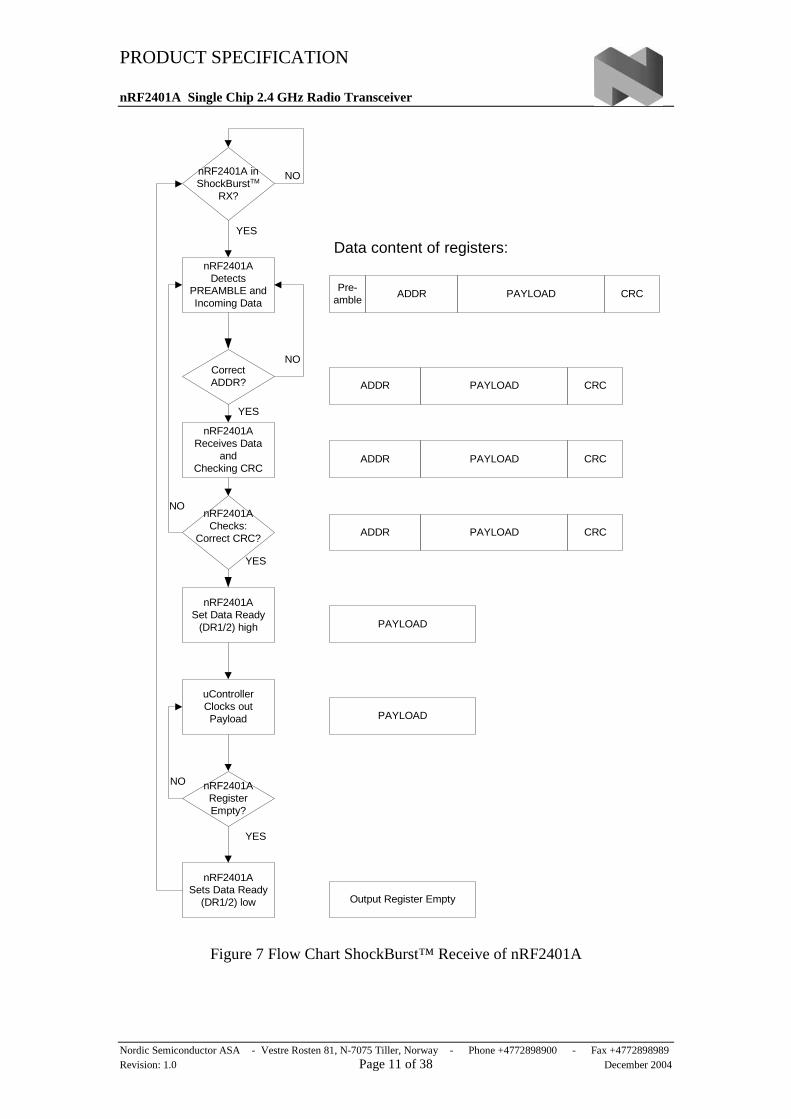
CorrectADDR?
nRF2401ADetects
PREAMBLE andIncoming Data
nRF2401ASet Data Ready
(DR1/2) high
YES
YES
NO
NO
nRF2401AReceives Data
andChecking CRC
ADDR PAYLOAD CRC
ADDR PAYLOAD CRC
ADDR PAYLOAD CRC
Pre-amble
ADDR PAYLOAD CRC
PAYLOAD
uControllerClocks outPayload PAYLOAD
Data content of registers:
nRF2401ARegisterEmpty?
nRF2401ASets Data Ready
(DR1/2) low
NO
YES
Output Register Empty
nRF2401A inShockBurstTM
RX?
YES
NO
nRF2401AChecks:
Correct CRC?
Figure 7 Flow Chart ShockBurst™ Receive of nRF2401A
PRODUCT SPECIFICATION nRF2401A Single Chip 2.4 GHz Radio Transceiver
Nordic Semiconductor ASA - Vestre Rosten 81, N-7075 Tiller, Norway - Phone +4772898900 - Fax +4772898989 Revision: 1.0 Page 12 of 38 December 2004
nRF2401A ShockBurst™ Receive: MCU interface pins: CE, DR1, CLK1 and DATA (one RX channel receive)
1. Correct address and size of payload of incoming RF packages are set when nRF2401A is configured to ShockBurst™ RX.
2. To activate RX, set CE high. 3. After 200 µs settling, nRF2401A is monitoring the air for incoming
communication. 4. When a valid package has been received (correct address and CRC found),
nRF2401A removes the preamble, address and CRC bits. 5. nRF2401A then notifies (interrupts) the MCU by setting the DR1 pin high. 6. MCU may (or may not) set the CE low to disable the RF front end (low
current mode). 7. The MCU will clock out just the payload data at a suitable rate (ex. 10
kbps). 8. When all payload data is retrieved nRF2401A sets DR1 low again, and is
ready for new incoming data package if CE is kept high during data download. If the CE was set low, a new start up sequence can begin, see Figure 16.
Direct Mode In direct mode the nRF2401A works like a traditional RF device. Data must be at 1Mbps ±200ppm, or 250kbps ±200ppm at low data rate setting, for the receiver to detect the signals. Direct Mode Transmit: MCU interface pins: CE, DATA
1. When application MCU has data to send, set CE high 2. The nRF2401A RF front end is now immediately activated, and after 200
µs settling time, data will modulate the carrier directly. 3. All RF protocol parts must hence be implemented in MCU firmware
(preamble, address and CRC). Direct Mode Receive: MCU interface pins: CE, CLK1, and DATA
1. Once the nRF2401A is configured and powered up (CE high) in direct RX mode, DATA will start to toggle due to noise present on the air.
2. CLK1 will also start to toggle as nRF2401A is trying to lock on to the incoming data stream.
3. Once a valid preamble arrives, CLK1 and DATA will lock on to the incoming signal and the RF package will appear at the DATA pin with the same speed as it is transmitted.
4. To enable the demodulator to re-generate the clock, the preamble must be 8 bits toggling hi-low, starting with low if the first data bit is low.
5. In this mode no data ready (DR) signals is available. Address and checksum verification must also be done in the receiving MCU.

PRODUCT SPECIFICATION nRF2401A Single Chip 2.4 GHz Radio Transceiver
Nordic Semiconductor ASA - Vestre Rosten 81, N-7075 Tiller, Norway - Phone +4772898900 - Fax +4772898989 Revision: 1.0 Page 13 of 38 December 2004
DuoCeiver™ Simultaneous Two Channel Receive Mode In both ShockBurst™ & direct modes the nRF2401A can facilitate simultaneous reception of two parallel independent frequency channels at the maximum data rate. This means:
• nRF2401A can receive data from two 1 Mbps transmitters (ex: nRF2401A or nRF2402) 8 MHz (8 frequency channels) apart through one antenna interface.
• The output from the two data channels is fed to two separate MCU interfaces. • Data channel 1: CLK1, DATA, and DR1 • Data channel 2: CLK2, DOUT2, and DR2 • DR1 and DR2 are available only in ShockBurst™.
The nRF2401A DuoCeiver™ technology provides 2 separate dedicated data channels for RX and replaces the need for two, stand alone receiver systems.
nRF2401ATx/Rx
nRF2401ATx/Rx
nRF2401ATx/Rx
Figure 8 Simultaneous 2 channel receive on nRF2401A
There is one absolute requirement for using the second data channel. For the nRF2401A to be able to receive at the second data channel the frequency channel must be 8MHz higher than the frequency of data channel 1. The nRF2401A must be programmed to receive at the frequency of data channel 1. No time multiplexing is used in nRF2401A to fulfil this function. In direct mode the MCU must be able to handle two simultaneously incoming data packets if it is not multiplexing between the two data channels. In ShockBurst™ it is possible for the MCU to clock out one data channel at a time while data on the other data channel waits for MCU availability, without any lost data packets, and by doing so reduce the needed performance of the MCU.
FRF1
FRF2=FRF1+8MHzClock
Recovery,DataSlicer
ADDR,CRC
Check
ClockRecovery,DataSlicer
ADDR,CRC
Check
DR1
DR2
CLK1DATA
CLK2DOUT2
Data(FRF1)
Data(FRF2)
Figure 9 DuoCeiverTM with two simultaneously independent receive channels.

PRODUCT SPECIFICATION nRF2401A Single Chip 2.4 GHz Radio Transceiver
Nordic Semiconductor ASA - Vestre Rosten 81, N-7075 Tiller, Norway - Phone +4772898900 - Fax +4772898989 Revision: 1.0 Page 14 of 38 December 2004
Configuration Mode In configuration mode a configuration word of up to 15 bytes is downloaded to nRF2401A. This is done through a simple 3-wire interface (CS, CLK1 and DATA). For more information on configuration please refer to the nRF2401A Device configuration chapter on page16.
Stand-By Mode Stand by mode is used to minimize average current consumption while maintaining short start up times. In this mode, part of the crystal oscillator is active. Current consumption is dependent on crystal frequency (Ex: 12 µA @ 4 MHz, 32 µA @ 16 MHz). The configuration word content is maintained during stand by.
Power Down Mode In power down the nRF2401A is disabled with minimal current consumption, typically less than 1µA. Entering this mode when the device is not active minimizes average current consumption, maximizing battery lifetime. The configuration word content is maintained during power down.

PRO
DU
CT
SPE
CIF
ICA
TIO
N
nRF
2401
A S
ingl
e C
hip
2.4
GH
z R
adio
Tra
nsce
iver
Nor
dic
Sem
icon
duct
or A
SA
- V
estr
e R
oste
n 81
, N-7
075
Till
er, N
orw
ay
- Ph
one
+477
2898
900
- Fa
x +
4772
8989
89
Rev
isio
n: 1
.0
Pag
e 15
of
38
Dec
embe
r 20
04
Pin
con
figu
rati
on f
or t
he d
iffe
rent
mod
es o
f nR
F24
01A
M
OD
E S
WIT
CH
ES
INP
UT
PIN
S B
IDIR
PIN
S O
UT
PU
T P
INS
dire
ctio
n di
rect
ion
dire
ctio
n nR
F24
01A
M
OD
ES
RX
MO
DE
Sh
ockB
urst
P
WR
_UP
C
E
CS
CL
K1
DA
TA
C
LK
2 D
R1
DR
2 D
OU
T2
In
In
In
Pow
er d
own
X
X
0 X
1 1
X
X
X
0 0
0 In
In
In
Po
wer
dow
n 0
1 0
X
0 X
X
X
0
0 0
In
In
In
Pow
er d
own
1 1
0 X
0
CL
K
X
X
0 0
0 In
In
In
St
and
by
0 X
1
0 0
X
X
X
0 0
0 In
In
In
St
and
by
1 0
1 0
0 X
X
X
0
0 0
In
In2
In
Stan
d by
1
1 1
0 0
CL
K
DA
TA
X
0
DR
2 0
In
Out
3 In
Stan
d by
1
1 1
0 0
CL
K
DA
TA
X
1
DR
2 0
In
In
In
Con
figu
ratio
n X
X
1
0 1
CL
K
CO
NFI
G D
AT
A
X
0 0
0 In
In
In
T
X S
hock
Bur
st™
0
1 1
1 0
CL
K
DA
TA
X
0
0 0
In
In
In
TX
Dir
ect
0 0
1 1
0 X
D
AT
A
X
0 0
0 In
O
ut
In
RX
Sho
ckB
urst
™
in o
ne c
hann
el
1 1
1 1
0 C
LK
D
AT
A
X
DR
1 0
0 In
O
ut
In
RX
Sho
ckB
urst
™
in tw
o ch
anne
ls
1 1
1 1
0 C
LK
D
AT
A
CL
K
DR
1 D
R2
DA
TA
O
ut
Out
O
ut
RX
Dir
ect
in o
ne c
hann
el
1 0
1 1
0 C
LK
D
AT
A
0 0
0 0
Out
O
ut
Out
R
X D
irec
t in
two
chan
nels
1
0 1
1 0
CL
K
DA
TA
C
LK
0
0 D
AT
A
Tab
le 7
Pin
con
figu
ratio
n of
nR
F240
1A.
1 In
= X
mea
ns th
e in
put s
houl
d be
set
to e
ither
“lo
w”
or “
high
”.
2 In
put i
f D
R1
is “
low
”.
3 O
utpu
t if
DR
1 is
“hi
gh”

PRODUCT SPECIFICATION nRF2401A Single Chip 2.4 GHz Radio Transceiver
Nordic Semiconductor ASA - Vestre Rosten 81, N-7075 Tiller, Norway - Phone +4772898900 - Fax +4772898989 Revision: 1.0 Page 16 of 38 December 2004
DEVICE CONFIGURATION All configuration of the nRF2401A is done via a 3-wire interface to a single configuration register. The configuration word can be up to 15 bytes long for ShockBurst™ use and up to 2 bytes long for direct mode.
Configuration for ShockBurst™ operation The configuration word in ShockBurst™ enables the nRF2401A to handle the RF protocol. Once the protocol is completed and loaded into nRF2401A only one byte, bit[7:0], needs to be updated during actual operation. The configuration blocks dedicated to ShockBurst™ is as follows:
• Payload section width: Specifies the number of payload bits in a RF package. This enables the nRF2401A to distinguish between payload data and the CRC bytes in a received package.
• Address width: Sets the number of bits used for address in the RF package. This enables the nRF2401A to distinguish between address and payload data.
• Address (RX Channel 1 and 2): Destination address for received data. • CRC: Enables nRF2401A on-chip CRC generation and de-coding.
NOTE: These configuration blocks, with the exception of the CRC, are dedicated for the packages that a nRF2401A is to receive. In TX mode, the MCU must generate an address and a payload section that fits the configuration of the nRF2401A that is to receive the data. When using the nRF2401A on-chip CRC feature ensure that CRC is enabled and uses the same length for both the TX and RX devices.
PRE-AMBLE ADDRESS PAYLOAD CRC
Figure 10 Data packet set-up
Configuration for Direct Mode operation For direct mode operation only the two first bytes (bit[15:0]) of the configuring word are relevant.

PRODUCT SPECIFICATION nRF2401A Single Chip 2.4 GHz Radio Transceiver
Nordic Semiconductor ASA - Vestre Rosten 81, N-7075 Tiller, Norway - Phone +4772898900 - Fax +4772898989 Revision: 1.0 Page 17 of 38 December 2004
Configuration Word overview
Bit position
Number of bits
Name Function
143:120 24 TEST Reserved for testing
119:112 8 DATA2_W Length of data payload section RX channel 2
111:104 8 DATA1_W Length of data payload section RX channel 1
103:64 40 ADDR2 Up to 5 byte address for RX channel 2
63:24 40 ADDR1 Up to 5 byte address for RX channel 1
23:18 6 ADDR_W Number of address bits (both RX channels).
17 1 CRC_L 8 or 16 bit CRC
Shoc
kBur
st™
con
figu
rati
on
16 1 CRC_EN Enable on-chip CRC generation/checking.
15 1 RX2_EN Enable two channel receive mode
14 1 CM Communication mode (Direct or ShockBurst™)
13 1 RFDR_SB RF data rate (1Mbps requires 16MHz crystal)
12:10 3 XO_F Crystal frequency
9:8 2 RF_PWR RF output power
7:1 7 RF_CH# Frequency channel Gen
eral
dev
ice
conf
igur
atio
n
0 1 RXEN RX or TX operation
Table 8 Table of configuration words.
The configuration word is shifted in MSB first on positive CLK1 edges. New configuration is enabled on the falling edge of CS. NOTE. On the falling edge of CS, the nRF2401A updates the number of bits actually shifted in during the last configuration. Ex: If the nRF2401A is to be configured for 2 channel RX in ShockBurst™, a total of 120 bits must be shifted in during the first configuration after VDD is applied. Once the wanted protocol, modus and RF channel are set, only one bit (RXEN) is shifted in to switch between RX and TX.

PRODUCT SPECIFICATION nRF2401A Single Chip 2.4 GHz Radio Transceiver
Nordic Semiconductor ASA - Vestre Rosten 81, N-7075 Tiller, Norway - Phone +4772898900 - Fax +4772898989 Revision: 1.0 Page 18 of 38 December 2004
Configuration Word Detailed Description The following describes the function of the 144 bits (bit 143 = MSB) that is used to configure the nRF2401A. General Device Configuration: bit[15:0] ShockBurst™ Configuration: bit[119:16] Test Configuration: bit[143:120] MSB TEST
D143 D142 D141 D140 D139 D138 D137 D136 Reserved for testing
1 0 0 0 1 1 1 0 Default
MSB TEST D135 D134 D133 D132 D131 D130 D129 D128 D127 D126 D125 D124 D123 D122 D121 D120
Reserved for testing Close PLL in TX 0 0 0 0 1 0 0 0 0 0 0 1 1 1 0 0 Default
DATA2_W
D119 D118 D117 D116 D115 D114 D113 D112 Data width channel#2 in # of bits excluding addr/crc
0 0 1 0 0 0 0 0 Default
DATA1_W
D111 D110 D109 D108 D107 D106 D105 D104 Data width channel#1 in # of bits excluding addr/crc
0 0 1 0 0 0 0 0 Default
ADDR2
D103 D102 D101 …. D71 D70 D69 D68 D67 D66 D65 D64 Channel#2 Address RX (up to 40bit)
0 0 0 … 1 1 1 0 0 1 1 1 Default
ADDR1
D63 D62 D61 …. D31 D30 D29 D28 D27 D26 D25 D24 Channel#1 Address RX (up to 40bit)
0 0 0 … 1 1 1 0 0 1 1 1 Default
ADDR_W
D23 D22 D21 D20 D19 D18 Address width in # of bits (both channels)
0 0 1 0 0 0 Default
CRC
D17 D16 CRC Mode 1 = 16bit, 0 = 8bit CRC 1 = enable; 0 = disable
0 1 Default
RF-Programming LSB
D15 D14 D13 D12 D11 D10 D9 D8 D7 D6 D5 D4 D3 D2 D1 D0 Two Ch. BUF OD XO Frequency RF Power Channel selection RXEN
0 0 0 0 1 1 1 1 0 0 0 0 0 1 0 0 Default
Table 9 Configuration data word
The MSB bit should be loaded first into the configuration register. Default configuration word: h8E08.1C20.2000.0000.00E7.0000.0000.E721.0F04.
PRODUCT SPECIFICATION nRF2401A Single Chip 2.4 GHz Radio Transceiver
Nordic Semiconductor ASA - Vestre Rosten 81, N-7075 Tiller, Norway - Phone +4772898900 - Fax +4772898989 Revision: 1.0 Page 19 of 38 December 2004
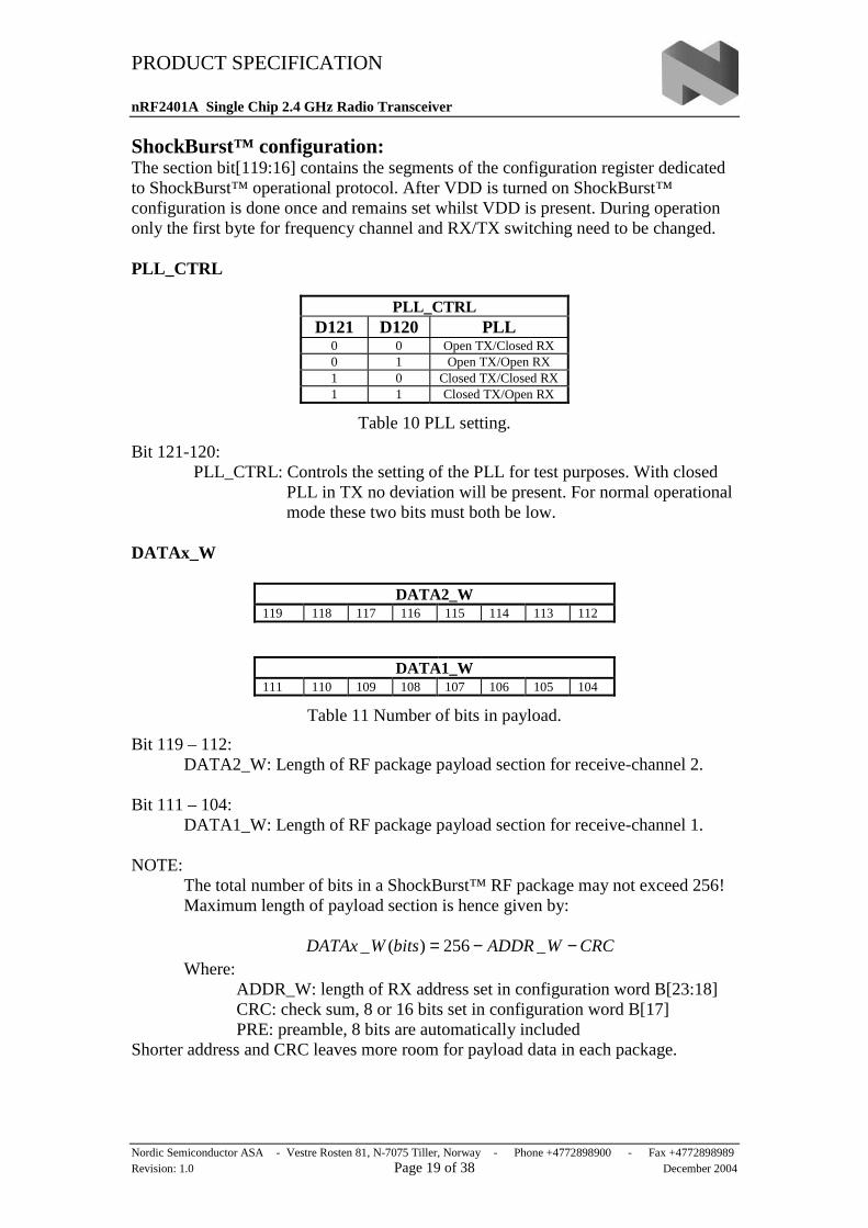
ShockBurst™ configuration: The section bit[119:16] contains the segments of the configuration register dedicated to ShockBurst™ operational protocol. After VDD is turned on ShockBurst™ configuration is done once and remains set whilst VDD is present. During operation only the first byte for frequency channel and RX/TX switching need to be changed. PLL_CTRL
PLL_CTRL D121 D120 PLL
0 0 Open TX/Closed RX 0 1 Open TX/Open RX 1 0 Closed TX/Closed RX 1 1 Closed TX/Open RX
Table 10 PLL setting.
Bit 121-120: PLL_CTRL: Controls the setting of the PLL for test purposes. With closed
PLL in TX no deviation will be present. For normal operational mode these two bits must both be low.
DATAx_W
DATA2_W
119 118 117 116 115 114 113 112
DATA1_W 111 110 109 108 107 106 105 104
Table 11 Number of bits in payload.
Bit 119 – 112: DATA2_W: Length of RF package payload section for receive-channel 2.
Bit 111 – 104: DATA1_W: Length of RF package payload section for receive-channel 1.
NOTE: The total number of bits in a ShockBurst™ RF package may not exceed 256! Maximum length of payload section is hence given by:
CRCWADDRbitsWDATAx −−= _256)(_ Where:
ADDR_W: length of RX address set in configuration word B[23:18] CRC: check sum, 8 or 16 bits set in configuration word B[17] PRE: preamble, 8 bits are automatically included
Shorter address and CRC leaves more room for payload data in each package.

PRODUCT SPECIFICATION nRF2401A Single Chip 2.4 GHz Radio Transceiver
Nordic Semiconductor ASA - Vestre Rosten 81, N-7075 Tiller, Norway - Phone +4772898900 - Fax +4772898989 Revision: 1.0 Page 20 of 38 December 2004
ADDRx
ADDR2 103 102 101 …. 71 70 69 68 67 66 65 64
ADDR1
63 62 61 …. 31 30 29 28 27 26 25 24
Table 12 Address of receiver #2 and receiver #1.
Bit 103 – 64:
ADDR2: Receiver address channel 2, up to 40 bit. Bit 63 – 24: ADDR1
ADDR1: Receiver address channel 1, up to 40 bit. NOTE!
Bits in ADDRx exceeding the address width set in ADDR_W are redundant and can be set to logic 0.
ADDR_W & CRC
ADDR_W CRC_L CRC_EN 23 22 21 20 19 18 17 16
Table 13 Number of bits reserved for RX address + CRC setting.
Bit 23 – 18:
ADDR_W: Number of bits reserved for RX address in ShockBurst™ packages.
NOTE:
Maximum number of address bits is 40 (5 bytes). Values over 40 in ADDR_W are not valid.
Bit 17:
CRC_L: CRC length to be calculated by nRF2401A in ShockBurst™. Logic 0: 8 bit CRC Logic 1: 16 bit CRC
Bit: 16:
CRC_EN: Enables on-chip CRC generation (TX) and verification (RX). Logic 0: On-chip CRC generation/checking disabled Logic 1: On-chip CRC generation/checking enabled
NOTE:
An 8 bit CRC will increase the number of payload bits possible in each ShockBurst™ data packet, but will also reduce the system integrity.

PRODUCT SPECIFICATION nRF2401A Single Chip 2.4 GHz Radio Transceiver
Nordic Semiconductor ASA - Vestre Rosten 81, N-7075 Tiller, Norway - Phone +4772898900 - Fax +4772898989 Revision: 1.0 Page 21 of 38 December 2004
General device configuration: This section of the configuration word handles RF and device related parameters. Modes:
RX2_EN CM RFDR_SB XO_F RF_PWR 15 14 13 12 11 10 9 8
Table 14 RF operational settings.
Bit 15: RX2_EN: Logic 0: One channel receive Logic 1: Two channels receive NOTE:
In two channels receive, the nRF2401A receives on two, separate frequency channels simultaneously. The frequency of receive channel 1 is set in the configuration word bit[7-1], receive channel 2 is always 8 channels (8 MHz) above receive channel 1.
Bit 14:
Communication Mode: Logic 0: nRF2401A operates in direct mode.
Logic 1: nRF2401A operates in ShockBurst™ mode Bit 13:
RF Data Rate: Logic 0: 250 kbps Logic 1: 1 Mbps
NOTE:
Utilizing 250 kbps instead of 1Mbps will improve the receiver sensitivity by 10 dB. 1Mbps requires 16MHz crystal.
Bit 12-10:
XO_F: Selects the nRF2401A crystal frequency to be used:
XO FREQUENCY SELECTION D12 D11 D10 Crystal Frequency [MHz]
0 0 0 4 0 0 1 8 0 1 0 12 0 1 1 16 1 0 0 20
Table 15 Crystal frequency setting.
PRODUCT SPECIFICATION nRF2401A Single Chip 2.4 GHz Radio Transceiver
Nordic Semiconductor ASA - Vestre Rosten 81, N-7075 Tiller, Norway - Phone +4772898900 - Fax +4772898989 Revision: 1.0 Page 22 of 38 December 2004
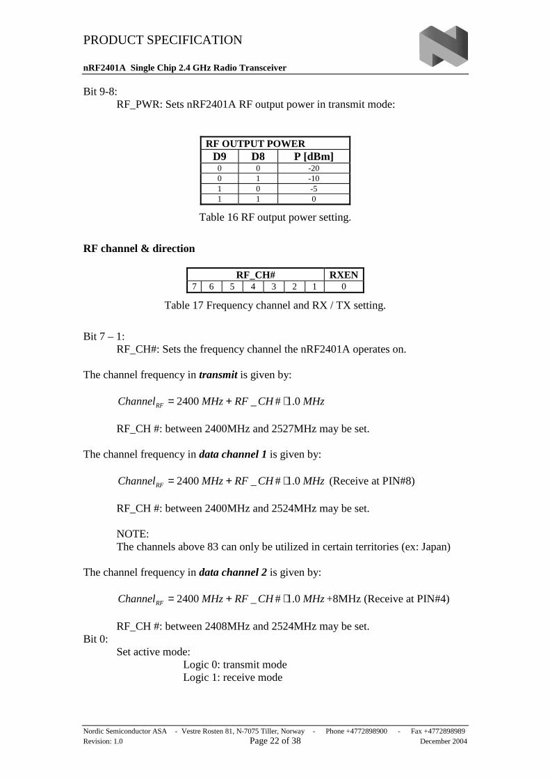
Bit 9-8: RF_PWR: Sets nRF2401A RF output power in transmit mode:
RF OUTPUT POWER D9 D8 P [dBm]
0 0 -20 0 1 -10 1 0 -5 1 1 0
Table 16 RF output power setting.
RF channel & direction
RF_CH# RXEN
7 6 5 4 3 2 1 0
Table 17 Frequency channel and RX / TX setting.
Bit 7 – 1:
RF_CH#: Sets the frequency channel the nRF2401A operates on. The channel frequency in transmit is given by:
MHzCHRFMHzChannelRF 0.1#_2400 ⋅+=
RF_CH #: between 2400MHz and 2527MHz may be set.
The channel frequency in data channel 1 is given by:
MHzCHRFMHzChannelRF 0.1#_2400 ⋅+= (Receive at PIN#8)
RF_CH #: between 2400MHz and 2524MHz may be set. NOTE: The channels above 83 can only be utilized in certain territories (ex: Japan)
The channel frequency in data channel 2 is given by:
MHzCHRFMHzChannelRF 0.1#_2400 ⋅+= +8MHz (Receive at PIN#4)
RF_CH #: between 2408MHz and 2524MHz may be set. Bit 0:
Set active mode: Logic 0: transmit mode Logic 1: receive mode

PRODUCT SPECIFICATION nRF2401A Single Chip 2.4 GHz Radio Transceiver
Nordic Semiconductor ASA - Vestre Rosten 81, N-7075 Tiller, Norway - Phone +4772898900 - Fax +4772898989 Revision: 1.0 Page 23 of 38 December 2004
DATA PACKAGE DESCRIPTION
PRE-AMBLE ADDRESS PAYLOAD CRC
Figure 11 Data Package Diagram
The data packet for both ShockBurst™ mode and direct mode communication is divided into 4 sections. These are: 1. PREAMBLE • The preamble field is required in ShockBurst™ and Direct modes.
• Preamble is 8 bits in length and is dependent of the first data bit in direct mode. PREAMBLE 1st ADDR-BIT
01010101 0 10101010 1
• Preamble is automatically added to the data packet in ShockBurst™ and thereby gives extra space for payload. In Direct mode MCU must handle preamble.
In ShockBurst™ mode RX, the preamble is removed from the received output data, in direct mode the preamble is transparent to the output data.
2 ADDRESS • The address field is required in ShockBurst™ mode.1 • 8 to 40 bits length. • Address automatically removed from received packet in ShockBurst™
mode. In Direct mode MCU must handle address.
3 PAYLOAD • The data to be transmitted • In ShockBurst™ mode payload size is 256 bits minus the following:
(Address: 8 to 40 bits. + CRC 8 or 16 bits). • In Direct mode the maximum packet size (length) is for 1Mbps 4000 bits
(4ms).
4 CRC • The CRC is optional in ShockBurst™ mode, and is not used in Direct mode.
• 8 or 16 bits length • The CRC is removed from the received output data in ShockBurst™ RX.
Table 18 Data package description
1 Suggestions for the use of addresses in ShockBurst™: In general more bits in the address gives less false detection, which in the end may give lower data packet loss. A. The address made by (5, 4, 3, or 2) equal bytes are not recommended because it in general will
make the packet-error-rate increase. B. Addresses where the level shift only one time (i.e. 000FFFFFFF) could often be detected in noise
that may give a false detection, which again may give raised packet-error-rate. Direct mode will be dependent on the software used in the MCU, but it is recommended to have the same restrictions on addresses for this mode.

PRODUCT SPECIFICATION nRF2401A Single Chip 2.4 GHz Radio Transceiver
Nordic Semiconductor ASA - Vestre Rosten 81, N-7075 Tiller, Norway - Phone +4772898900 - Fax +4772898989 Revision: 1.0 Page 24 of 38 December 2004
IMPORTANT TIMING DATA The following timing applies for operation of nRF2401A.
nRF2401A Timing Information
nRF2401A timing Max. Min. Name PWR_DWN Configuration mode 3ms Tpd2cfgm PWR_DWN Active mode (RX/TX) 3ms Tpd2a ST_BY TX ShockBurst™ 195µs Tsby2txSB ST_BY TX Direct Mode 202µs Tsby2txDM ST_BY RX mode 202µs Tsby2rx Minimum delay from CS to data. 5µs Tcs2data Minimum delay from CE to data. 5µs Tce2data Minimum delay from DR1/2 to clk. 50ns Tdr2clk Maximum delay from clk to data. 50ns Tclk2data Delay between edges 50ns Td Setup time 500ns Ts Hold time 500ns Th Delay to finish internal GFSK data 1/data rate Tfd Minimum input clock high 500ns Thmin Set-up of data in Direct Mode 50ns Tsdm Minimum clock high in Direct Mode 300ns Thdm Minimum clock low in Direct Mode 230ns Tldm Time on air, TX Direct mode 4ms ToaDM
Table 19 Operational timing of nRF2401A
When the nRF2401A is in power down it must always settle in stand by for 3ms before it can enter configuration or one of the active modes.
PWR_UP
DATA
CE
Tpd2cfgm
CLK1
CS
Figure 12 Timing diagram for power down (or VDD off) to configuration mode for nRF2401A.

PRODUCT SPECIFICATION nRF2401A Single Chip 2.4 GHz Radio Transceiver
Nordic Semiconductor ASA - Vestre Rosten 81, N-7075 Tiller, Norway - Phone +4772898900 - Fax +4772898989 Revision: 1.0 Page 25 of 38 December 2004
PWR_UP
DATA
CE
Tpd2a
CLK1
CS
Figure 13 Power down (or VDD off) to active mode
Note that the configuration word will be lost when VDD is turned off and that the device then must be configured before going to one of the active modes. If the device is configured one can go directly from power down to the wanted active mode. Note:
CE and CS may not be high at the same time. Setting one or the other decides whether configuration or active mode is entered.

PRODUCT SPECIFICATION nRF2401A Single Chip 2.4 GHz Radio Transceiver
Nordic Semiconductor ASA - Vestre Rosten 81, N-7075 Tiller, Norway - Phone +4772898900 - Fax +4772898989 Revision: 1.0 Page 26 of 38 December 2004
Configuration mode timing When one or more of the bits in the configuration word needs to be changed the following timing apply.
CS
CLK1
DATA
CE
PWR_UP
CLK1
DATA
CS
MSB
Ts
CE
Th
t = 0
Td
Thmin
Tcs
2dat
a
Figure 14 Timing diagram for configuration of nRF2401A
If configuration mode is entered from power down, CS can be set high after Tpd2sby as shown in Figure 12.
PRODUCT SPECIFICATION nRF2401A Single Chip 2.4 GHz Radio Transceiver
Nordic Semiconductor ASA - Vestre Rosten 81, N-7075 Tiller, Norway - Phone +4772898900 - Fax +4772898989 Revision: 1.0 Page 27 of 38 December 2004
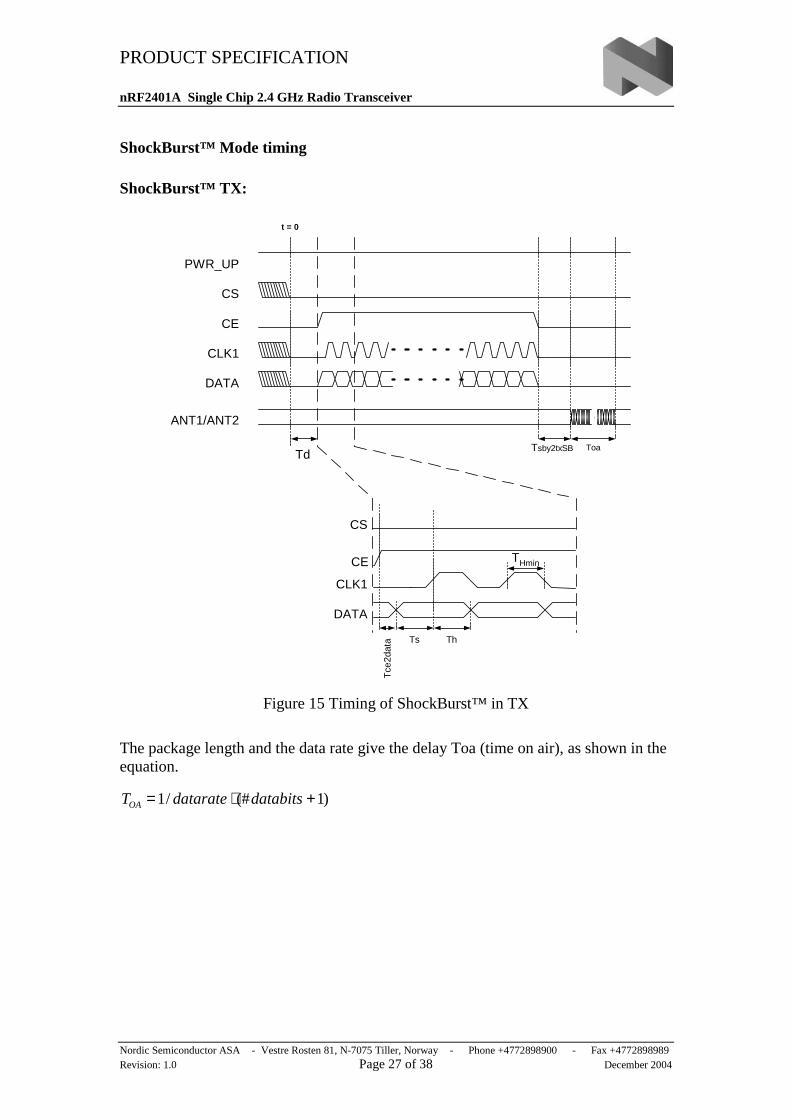
ShockBurst™ Mode timing ShockBurst™ TX:
CS
CLK1
DATA
CE
PWR_UP
CLK1
DATA
CS
Th
Tce
2dat
a
CE
Td
ANT1/ANT2 .
Tsby2txSB Toa
t = 0
THmin
Ts
Figure 15 Timing of ShockBurst™ in TX
The package length and the data rate give the delay Toa (time on air), as shown in the equation.
)1(#/1 +⋅= databitsdatarateTOA

PRODUCT SPECIFICATION nRF2401A Single Chip 2.4 GHz Radio Transceiver
Nordic Semiconductor ASA - Vestre Rosten 81, N-7075 Tiller, Norway - Phone +4772898900 - Fax +4772898989 Revision: 1.0 Page 28 of 38 December 2004
ShockBurst™ RX:
Figure 16 Timing of ShockBurst™ in RX
The CE may be kept high during downloading of data, but the cost is higher current consumption (18mA) and the benefit is short start-up time (200µs) when DR1 goes low.
CS
CLK1/2
DATA/DOUT2
CE
PWR_UP
CLK1/2
DATA/DOUT2
CE
Tdr
2clk
DR1/2
Td
ANT1/ANT2 .
Tsby2rx
Tcl
k2da
ta
DR1/2
t = 0
Thmin
Td

PRODUCT SPECIFICATION nRF2401A Single Chip 2.4 GHz Radio Transceiver
Nordic Semiconductor ASA - Vestre Rosten 81, N-7075 Tiller, Norway - Phone +4772898900 - Fax +4772898989 Revision: 1.0 Page 29 of 38 December 2004
Direct Mode Direct Mode TX:
CS
CLK1
DATA
CE
PWR_UP
Td
ANT1/ANT2
Tsby2txDM ToaDM Tfd
t = 0
Figure 17 Timing of direct mode TX
In TX direct mode the input data will be sampled by nRF2401A and therefore no clock is needed. The clock must be stable at low level during transmission due to noise considerations. The exact delay Tsby2txDM is given by the equation:
usFusT XOtxDMsby 25.214/11942 +⋅+=
The maximum length of a package (ToaDM) over all voltages and temperatures is 4ms. This is limited by frequency drift in the transmitter and is independent of data rate and frequency channel.

PRODUCT SPECIFICATION nRF2401A Single Chip 2.4 GHz Radio Transceiver
Nordic Semiconductor ASA - Vestre Rosten 81, N-7075 Tiller, Norway - Phone +4772898900 - Fax +4772898989 Revision: 1.0 Page 30 of 38 December 2004
Direct Mode RX:
CS
CLK1/2
DATA/DOUT2
CE
PWR_UP
Td
ANT1/ANT2
Tsby2rx
CLK1/2
DATA/DOUT2
CE
Tsdm
t = 0
Thdm Tldm
Figure 18 Timing of direct mode RX
Tsby2rx describes the delay from the positive edge of CE to start detection of (demodulating) incoming data.
PRODUCT SPECIFICATION nRF2401A Single Chip 2.4 GHz Radio Transceiver
Nordic Semiconductor ASA - Vestre Rosten 81, N-7075 Tiller, Norway - Phone +4772898900 - Fax +4772898989 Revision: 1.0 Page 31 of 38 December 2004
PERIPHERAL RF INFORMATION
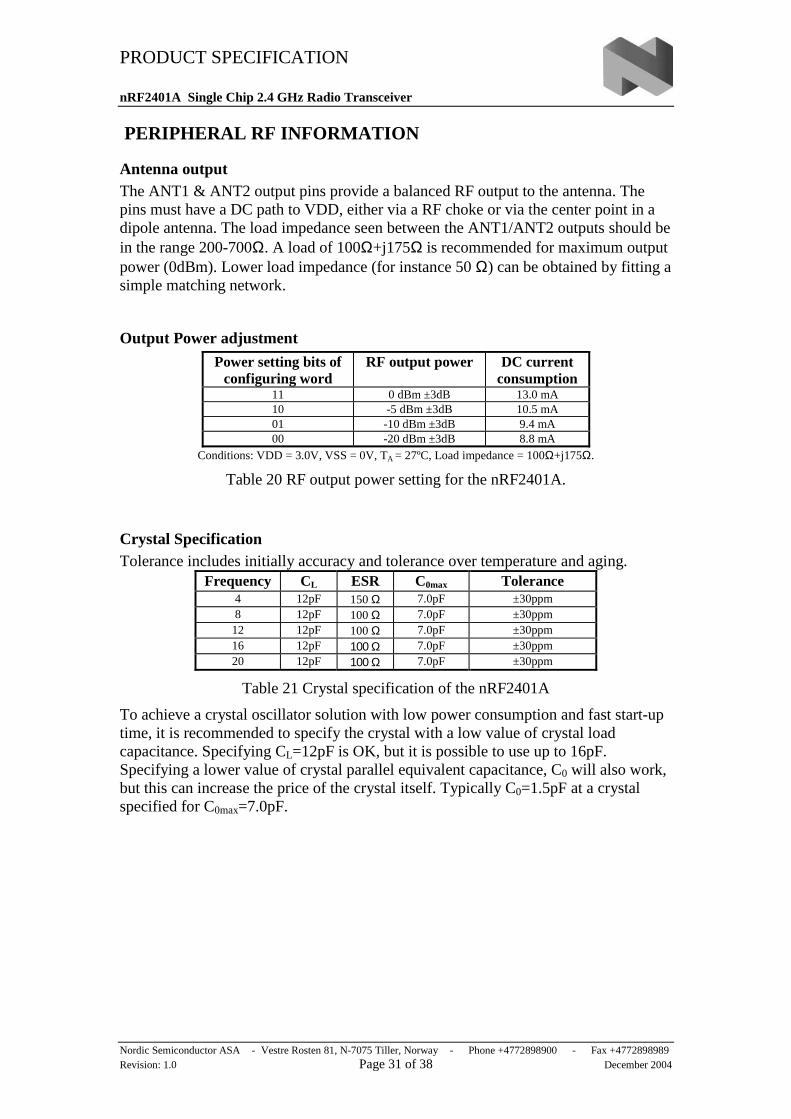
Antenna output The ANT1 & ANT2 output pins provide a balanced RF output to the antenna. The pins must have a DC path to VDD, either via a RF choke or via the center point in a dipole antenna. The load impedance seen between the ANT1/ANT2 outputs should be in the range 200-700Ω. A load of 100Ω+j175Ω is recommended for maximum output power (0dBm). Lower load impedance (for instance 50 Ω) can be obtained by fitting a simple matching network.
Output Power adjustment
Power setting bits of configuring word
RF output power DC current consumption
11 0 dBm ±3dB 13.0 mA 10 -5 dBm ±3dB 10.5 mA 01 -10 dBm ±3dB 9.4 mA 00 -20 dBm ±3dB 8.8 mA
Conditions: VDD = 3.0V, VSS = 0V, TA = 27ºC, Load impedance = 100Ω+j175Ω.
Table 20 RF output power setting for the nRF2401A.
Crystal Specification Tolerance includes initially accuracy and tolerance over temperature and aging.
Frequency CL ESR C0max Tolerance 4 12pF 150 Ω 7.0pF ±30ppm 8 12pF 100 Ω 7.0pF ±30ppm
12 12pF 100 Ω 7.0pF ±30ppm 16 12pF 100 Ω 7.0pF ±30ppm 20 12pF 100 Ω 7.0pF ±30ppm
Table 21 Crystal specification of the nRF2401A
To achieve a crystal oscillator solution with low power consumption and fast start-up time, it is recommended to specify the crystal with a low value of crystal load capacitance. Specifying CL=12pF is OK, but it is possible to use up to 16pF. Specifying a lower value of crystal parallel equivalent capacitance, C0 will also work, but this can increase the price of the crystal itself. Typically C0=1.5pF at a crystal specified for C0max=7.0pF.
PRODUCT SPECIFICATION nRF2401A Single Chip 2.4 GHz Radio Transceiver
Nordic Semiconductor ASA - Vestre Rosten 81, N-7075 Tiller, Norway - Phone +4772898900 - Fax +4772898989 Revision: 1.0 Page 32 of 38 December 2004
Sharing crystal with micro controller. When using a micro controller to drive the crystal reference input XC1 of the nRF2401A transceiver some rules must be followed.
Crystal parameters: When the micro controller drives the nRF2401A clock input, the requirement of load capacitance CL is set by the micro controller only. The frequency accuracy of 30 ppm is still required to get a functional radio link. The nRF2401A will load the crystal by 0.5pF at XC1 in addition to the PBC routing.
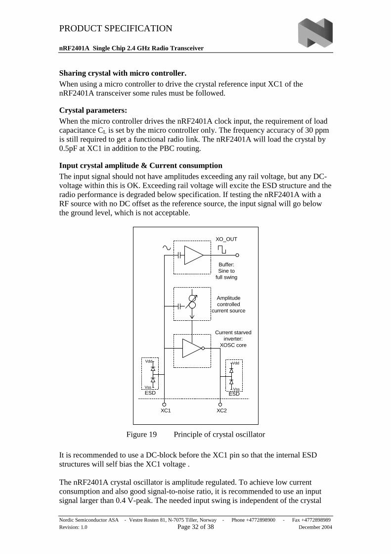
Input crystal amplitude & Current consumption The input signal should not have amplitudes exceeding any rail voltage, but any DC- voltage within this is OK. Exceeding rail voltage will excite the ESD structure and the radio performance is degraded below specification. If testing the nRF2401A with a RF source with no DC offset as the reference source, the input signal will go below the ground level, which is not acceptable.
XC1
XO_OUT
Amplitudecontrolled
current source
Buffer:Sine to
full swing
Current starvedinverter:
XOSC core
XC2
Vdd
Vss
Vdd
VssESDESD
Figure 19 Principle of crystal oscillator
It is recommended to use a DC-block before the XC1 pin so that the internal ESD structures will self bias the XC1 voltage . The nRF2401A crystal oscillator is amplitude regulated. To achieve low current consumption and also good signal-to-noise ratio, it is recommended to use an input signal larger than 0.4 V-peak. The needed input swing is independent of the crystal
PRODUCT SPECIFICATION nRF2401A Single Chip 2.4 GHz Radio Transceiver
Nordic Semiconductor ASA - Vestre Rosten 81, N-7075 Tiller, Norway - Phone +4772898900 - Fax +4772898989 Revision: 1.0 Page 33 of 38 December 2004
frequency. When clocking the nRF2401A externally, XC2 is not used and can be left as an open pin. Frequency Reference MCU In direct mode there is a requirement on the accuracy of the data rate. For the receiver to detect the incoming data and recover the clock, the data rate must be within ±200ppm, given that the data is "random", i.e. there is a statistical calculation on how often a preamble like sequence is present in the data. The clock is synchronized for any preamble detection, be it a dedicated preamble or part of the data stream.
PCB layout and de-coupling guidelines A well-designed PCB is necessary to achieve good RF performance. Keep in mind that a poor layout may lead to loss of performance, or even functionality, if due care is not taken. A fully qualified RF-layout for the nRF2401A and its surrounding components, including matching networks, can be downloaded from www.nordicsemi.no. A PCB with a minimum of two layers including a ground plane is recommended for optimum performance. The nRF2401A DC supply voltage should be de-coupled as close as possible to the VDD pins with high performance RF capacitors, see Table 22. It is preferable to mount a large surface mount capacitor (e.g. 4.7µF tantalum) in parallel with the smaller value capacitors. The nRF2401A supply voltage should be filtered and routed separately from the supply voltages of any digital circuitry. Long power supply lines on the PCB should be avoided. All device grounds, VDD connections and VDD bypass capacitors must be connected as close as possible to the nRF2401A IC. For a PCB with a topside RF ground plane, the VSS pins should be connected directly to the ground plane. For a PCB with a bottom ground plane, the best technique is to have via holes as close as possible to the VSS pads. One via hole should be used for each VSS pin. Full swing digital data or control signals should not be routed close to the crystal or the power supply lines.

PRODUCT SPECIFICATION nRF2401A Single Chip 2.4 GHz Radio Transceiver
Nordic Semiconductor ASA - Vestre Rosten 81, N-7075 Tiller, Norway - Phone +4772898900 - Fax +4772898989 Revision: 1.0 Page 34 of 38 December 2004
APPLICATION EXAMPLE
nRF2401A with single ended matching network
CE1
VD
D24
VSS18
VDD17
VSS_PA 16DR2
2
CLK23
DOUT24
CS5
DR16
CL
K1
7
DA
TA
8
DV
DD
9
VS
S10
XC
211
XC
112
ANT215
ANT114
VDD_PA 13IR
EF
19V
SS
20V
DD
21V
SS
22P
WR
_UP
23nRF2401
U1nRF2401QFN24/5X5
C222pF
L13.3nH
L2
10nHC81.0pF
C91.0pF
C51nF
C610nF
R222K
C42.2nF
xxx
xxx
xxx
C122pF
R1
1M
X1
16 MHz
C34.7pF
C733nF
RF I/OPWR_UP
CEDR2
CLK2DOUT2
CSDR1
CLK1DATA
VDD
C10
2.2pF
L3
5.6nH
L4
5.6nHC11
4.7pFxxx
Figure 20 nRF2401A schematic for RF layouts with single end 50Ω antenna
Component Description Size Value Toleranc
e Units
C1 Capacitor ceramic, 50V, NPO 0603 22 ±5% pF C2 Capacitor ceramic, 50V, NPO 0603 22 ±5% pF C3 Capacitor ceramic, 50V, NPO 0603 4.7 ±5% pF C4 Capacitor ceramic, 50V, X7R 0603 2.2 ±10% nF C5 Capacitor ceramic, 50V, X7R 0603 1.0 ±10% nF C6 Capacitor ceramic, 50V, X7R 0603 10 ±10% nF C7 Capacitor ceramic, 50V, X7R 0603 33 ±10% nF R1 Resistor 0603 1.0 ±1% MΩ R2 Resistor 0603 22 ±1% kΩ U1 nRF2401A transceiver QFN24 / 5x5 nRF2401A X1 Crystal, CL = 12pF,
ESR < 100 ohm LxWxH =
4.0x2.5x0.8 161) +/- 30 ppm MHz
L1 Inductor, wire wound 2) 0603 3.3 ± 5% nH L2 Inductor, wire wound 2) 0603 10 ± 5% nH L3 Inductor, wire wound 2) 0603 5.6 ± 5% nH L4 Inductor, wire wound 2) 0603 5.6 ± 5% nH C8 Ceramic capacitor, 50V, NP0 0603 1.0 ± 0.1 pF pF C9 Ceramic capacitor, 50V, NP0 0603 1.0 ± 0.1 pF pF
C10 Ceramic capacitor, 50V, NP0 0603 2.2 ± 0.25 pF pF C11 Ceramic capacitor, 50V, NP0 0603 4.7 ± 0.25 pF pF
Table 22 Recommended components (BOM) in nRF2401A with antenna matching network
1) nRF2401A can operate at several crystal frequencies, please refer to page 31. 2) Wire wound inductors are recommended, other can be used if their self-resonant frequency (SFR) is > 2.7 GHz

PRODUCT SPECIFICATION nRF2401A Single Chip 2.4 GHz Radio Transceiver
Nordic Semiconductor ASA - Vestre Rosten 81, N-7075 Tiller, Norway - Phone +4772898900 - Fax +4772898989 Revision: 1.0 Page 35 of 38 December 2004
PCB layout example Figure 21 shows a PCB layout example for the application schematic in Figure 20. A double-sided FR-4 board of 1.6mm thickness is used. This PCB has a ground plane on the bottom layer. Additionally, there are ground areas on the component side of the board to ensure sufficient grounding of critical components. A large number of via holes connect the top layer ground areas to the bottom layer ground plane.
Top silk screen
No components in bottom layer
Top view
Bottom view
Figure 21 nRF2401A RF layout with single ended connection to 50Ω antenna and 0603 size passive components

PRODUCT SPECIFICATION nRF2401A Single Chip 2.4 GHz Radio Transceiver
Nordic Semiconductor ASA - Vestre Rosten 81, N-7075 Tiller, Norway - Phone +4772898900 - Fax +4772898989 Revision: 1.0 Page 36 of 38 December 2004
DEFINITIONS
Data sheet status Objective product specification This data sheet contains target specifications for product development. Preliminary product specification
This data sheet contains preliminary data; supplementary data may be published from Nordic Semiconductor ASA later.
Product specification This data sheet contains final product specifications. Nordic Semiconductor ASA reserves the right to make changes at any time without notice in order to improve design and supply the best possible product.
Limiting values Stress above one or more of the limiting values may cause permanent damage to the device. These are stress ratings only and operation of the device at these or at any other conditions above those given in the Specifications sections of the specification is not implied. Exposure to limiting values for extended periods may affect device reliability.
Application information Where application information is given, it is advisory and does not form part of the specification.
Table 23. Definitions
Nordic Semiconductor ASA reserves the right to make changes without further notice to the product to improve reliability, function or design. Nordic Semiconductor ASA does not assume any liability arising out of the application or use of any product or circuits described herein. LIFE SUPPORT APPLICATIONS These products are not designed for use in life support appliances, devices, or systems where malfunction of these products can reasonably be expected to result in personal injury. Nordic Semiconductor ASA customers using or selling these products for use in such applications do so at their own risk and agree to fully indemnify Nordic Semiconductor ASA for any damages resulting from such improper use or sale. Product Specification: Revision Date: 23.12.2004. Data sheet order code: 231204-nRF2401A or 231204-nRF2401AG All rights reserved ®. Reproduction in whole or in part is prohibited without the prior written permission of the copyright holder.

PRODUCT SPECIFICATION nRF2401A Single Chip 2.4 GHz Radio Transceiver
Nordic Semiconductor ASA - Vestre Rosten 81, N-7075 Tiller, Norway - Phone +4772898900 - Fax +4772898989 Revision: 1.0 Page 37 of 38 December 2004
YOUR NOTES
PRODUCT SPECIFICATION nRF2401A Single Chip 2.4 GHz Radio Transceiver
Nordic Semiconductor ASA - Vestre Rosten 81, N-7075 Tiller, Norway - Phone +4772898900 - Fax +4772898989 Revision: 1.0 Page 38 of 38 December 2004
Nordic Semiconductor ASA – World Wide Distributors
For Your nearest dealer, please see http://www.nordicsemi.no
Main Office: Vestre Rosten 81, N-7075 Tiller, Norway
Phone: +47 72 89 89 00, Fax: +47 72 89 89 89
Visit the Nordic Semiconductor ASA website at http://www.nordicsemi.no