Embed Size (px)
Citation preview

CC1120
SWRS112D – REVISED MARCH 2013 Page 1 of 24
PRODUCTION DATA information is current as of publication date. Products conform to specifications per the terms of Texas Instruments standard warranty. Production processing does
not necessarily include testing of all parameters.
High Performance RF Transceiver for Narrowband Systems
Applications
Narrowband ultra low power wireless systems with channel spacing down to 12.5 kHz
170/315/433/868/915/920/950 MHz ISM/SRD band
Wireless Metering and Wireless Smart Grid (AMR and AMI)
IEEE 802.15.4g systems
Home and building automation
Wireless alarm and security systems
Industrial monitoring and control
Wireless healthcare applications
Wireless sensor networks and Active RFID
Private mobile radio
Regulations
Suitable for systems targeting compliance with:
Europe ETSI EN 300 220 ETSI EN 54-25
US FCC CFR47 Part 15 FCC CFR47 Part 90, 24 and 101
Japan ARIB RCR STD-T30 ARIB STD-T67
ARIB STD-T108
Key Features
High performance single chip transceiver
o Adjacent channel selectivity: 64 dB at 12.5 kHz offset
o Blocking performance: 91 dB at 10 MHz offset
o Excellent receiver sensitivity: -123 dBm at 1.2 kbps -110 dBm at 50 kbps -127 dBm using built-in coding gain
o Very low phase noise: -111 dBc/Hz at 10 kHz offset
Suitable for systems targeting ETSI category 1 compliance in 169 MHz and 433 MHz bands
High spectral efficiency (9.6 kbps in 12.5 kHz channel in compliance with FCC narrowbanding mandate)
Power Supply
o Wide supply voltage range (2.0 V – 3.6 V)
o Low current consumption:
- RX: 2 mA in RX Sniff Mode
- RX: 17 mA peak current in low power mode
- RX: 22 mA peak current in high performance mode
- TX: 45 mA at +14 dBm
o Power down: 0.3 μA
Programmable output power up to +16 dBm with 0.4 dB step size
Automatic output power ramping
Configurable data rates: 0 to 200 kbps
Supported modulation formats: 2-FSK, 2- GFSK, 4-FSK, 4-GFSK, MSK, OOK
WaveMatch: Advanced digital signal processing for improved sync detect performance
RoHS compliant 5x5mm QFN 32 package
Peripherals and Support Functions
Enhanced Wake-On-Radio functionality for automatic low-power receive polling
Separate 128-byte RX and TX FIFOs
Includes functions for antenna diversity support
Support for re-transmissions
Support for auto-acknowledge of received packets
TCXO support and control, also in power modes
Automatic Clear Channel Assessment (CCA) for listen-before-talk (LBT) systems
Built in coding gain support for increased range and robustness
Digital RSSI measurement
Support for seamless integration with the CC1190 for increased range giving up to 3 dB improvement in sensitivity and up to +27 dBm output power
Temperature sensor
Description
The CC1120 is a fully integrated single-chip radio transceiver designed for high performance at very low power and low voltage operation in cost effective wireless systems. All filters are integrated, removing the need for costly external SAW and IF filters. The device is mainly intended for the ISM (Industrial, Scientific and Medical) and SRD (Short Range Device) frequency bands at 164-192 MHz, 274-320 MHz, 410-480 MHz and 820-960 MHz.
The CC1120 provides extensive hardware support for packet handling, data buffering, burst transmissions, clear channel assessment, link quality indication and Wake-On-
Radio. The CC1120 main operating parameters can be controlled via an SPI interface. In a typical system, the
CC1120 will be used together with a microcontroller and only few external passive components.
CS
n
SO
(GP
IO1
)
DV
DD
AV
DD
_IF
RB
IAS
AV
DD
_R
F
GP
IO0
RESET_N
GPIO3
GPIO2
DVDD
VDD_GUARD
CC11205
4
3
2
1
LNA_P
LNA_N
DCPL_VCO
AVDD_SYNTH1
TRX_SW
19
20
21
22
23
AV
DD
_P
FD
_C
HP
XO
SC
_Q
2
XO
SC
_Q
1
DC
PL
_P
FD
_C
HP
27
28
29
30
31
DCPL 6
7
PA
18
17
26
25
159 10
11
12
13
14
SI
N.C
.
DC
PL
_X
OS
C
AV
DD
_X
OS
C
8SCLK
16
24
EX
T_
XO
SC
32
LPF0
LPF1
AV
DD
_S
YN
TH
2
GND
GROUND PAD

CC1120
SWRS112D – REVISED MARCH 2013 Page 2 of 24
PRODUCTION DATA information is current as of publication date. Products conform to specifications per the terms of Texas Instruments standard warranty. Production processing does
not necessarily include testing of all parameters.
Table of Contents
1 ELECTRICAL SPECIFICATIONS .................................................................................................... 3
1.1 ABSOLUTE MAX RATINGS ................................................................................................................ 3 1.2 GENERAL CHARACTERISTICS ............................................................................................................ 3 1.3 RF CHARACTERISTICS ...................................................................................................................... 3 1.4 REGULATORY STANDARDS ............................................................................................................... 4 1.5 CURRENT CONSUMPTION, STATIC MODES ........................................................................................ 5 1.6 CURRENT CONSUMPTION, TRANSMIT MODES ................................................................................... 5 1.7 CURRENT CONSUMPTION, RECEIVE MODES ...................................................................................... 6 1.8 RECEIVE PARAMETERS ..................................................................................................................... 6 1.9 TRANSMIT PARAMETERS ................................................................................................................. 12 1.10 PLL PARAMETERS .......................................................................................................................... 13 1.11 WAKE-UP AND TIMING ................................................................................................................... 14 1.12 32 MHZ CRYSTAL OSCILLATOR...................................................................................................... 14 1.13 32 MHZ CLOCK INPUT (TCXO) ...................................................................................................... 14 1.14 32 KHZ CLOCK INPUT ..................................................................................................................... 15 1.15 32 KHZ RC OSCILLATOR ................................................................................................................ 15 1.16 I/O AND RESET................................................................................................................................ 15 1.17 TEMPERATURE SENSOR................................................................................................................... 15
2 TYPICAL PERFORMANCE CURVES ............................................................................................ 16
3 PIN CONFIGURATION ..................................................................................................................... 19
4 BLOCK DIAGRAM ............................................................................................................................ 20
4.1 FREQUENCY SYNTHESIZER ............................................................................................................. 20 4.2 RECEIVER ....................................................................................................................................... 20 4.3 TRANSMITTER ................................................................................................................................. 21 4.4 RADIO CONTROL AND USER INTERFACE ......................................................................................... 21 4.5 ENHANCED WAKE-ON-RADIO (EWOR) ......................................................................................... 21 4.6 SNIFF MODE .................................................................................................................................... 21 4.7 ANTENNA DIVERSITY ..................................................................................................................... 22
5 TYPICAL APPLICATION CIRCUIT ............................................................................................... 23
6 HISTORY ............................................................................................................................................. 24

CC1120
SWRS112D – REVISED MARCH 2013 Page 3 of 24
PRODUCTION DATA information is current as of publication date. Products conform to specifications per the terms of Texas Instruments standard warranty. Production processing does
not necessarily include testing of all parameters.
1 Electrical Specifications
All measurements performed on CC1120EM_868_915 rev.1.0.1, CC1120EM_955 rev.1.2.1, CC1120EM_420_470 rev.1.0.1 or CC1120EM_169 rev.1.2
1.1 Absolute Max Ratings
Parameter Min Typ Max Unit Condition
Supply Voltage ("VDD") -0.3 3.9 V
Storage Temperature Range -40 125 °C
ESD 2000 V HBM
ESD 500 V CDM
Input RF level +10 dBm
Voltage on Any Digital Pin -0.3 VDD+0.3
max 3.9 V
Voltage on Analog Pins (including “DCPL” pins)
-0.3 2.0 V
1.2 General Characteristics
Parameter Min Typ Max Unit Condition
Voltage Supply Range 2.0 3.6 V
Temperature Range -40 85 °C
1.3 RF Characteristics
Parameter Min Typ Max Unit Condition
Frequency Bands
820 960 MHz
410 480 MHz
274 320 MHz Please see application note AN115 “Using the CC112x/CC1175 at 274 to 320 MHz” for more information
164 192 MHz
Frequency Resolution
30 Hz In 820-960 MHz band
15 Hz In 410-480 MHz band
6 Hz In 164-192 MHz band
Datarate 0 200 kbps Packet mode
0 100 kbps Transparent mode
Datarate Step Size 1e-4 bps

CC1120
SWRS112D – REVISED MARCH 2013 Page 4 of 24
PRODUCTION DATA information is current as of publication date. Products conform to specifications per the terms of Texas Instruments standard warranty. Production processing does
not necessarily include testing of all parameters.
1.4 Regulatory Standards
Performance Mode Frequency Band Suitable for compliance with Comments
High Performance Mode
820 – 960 MHz
ARIB T-96
ARIB T-108
ETSI EN 300 220 category 2
ETSI EN 54-25
FCC PART 101
FCC PART 24 SUBMASK D
FCC PART 15.247
FCC PART 15.249
FCC PART 90 MASK G
FCC PART 90 MASK J
Performance also suitable for systems targeting maximum allowed output power in the respective bands, using a
range extender such as the CC1190
410 – 480 MHz
ARIB T-67
ARIB RCR STD-30
ETSI EN 300 220 category 1
FCC PART 90 MASK D
FCC PART 90 MASK G
Performance also suitable for systems targeting maximum allowed output power in the respective bands, using a range extender
164 – 192 MHz ETSI EN 300 220 category 1
FCC PART 90 MASK D
Performance also suitable for systems targeting maximum allowed output power in the respective bands, using a range extender
Low Power Mode
820 – 960 MHz
ETSI EN 300 220 category 2
FCC PART 15.247
FCC PART 15.249
410 – 480 MHz ETSI EN 300 220 category 2
164 – 192 MHz ETSI EN 300 220 category 2
CC1120
SWRS112D – REVISED MARCH 2013 Page 5 of 24
PRODUCTION DATA information is current as of publication date. Products conform to specifications per the terms of Texas Instruments standard warranty. Production processing does
not necessarily include testing of all parameters.
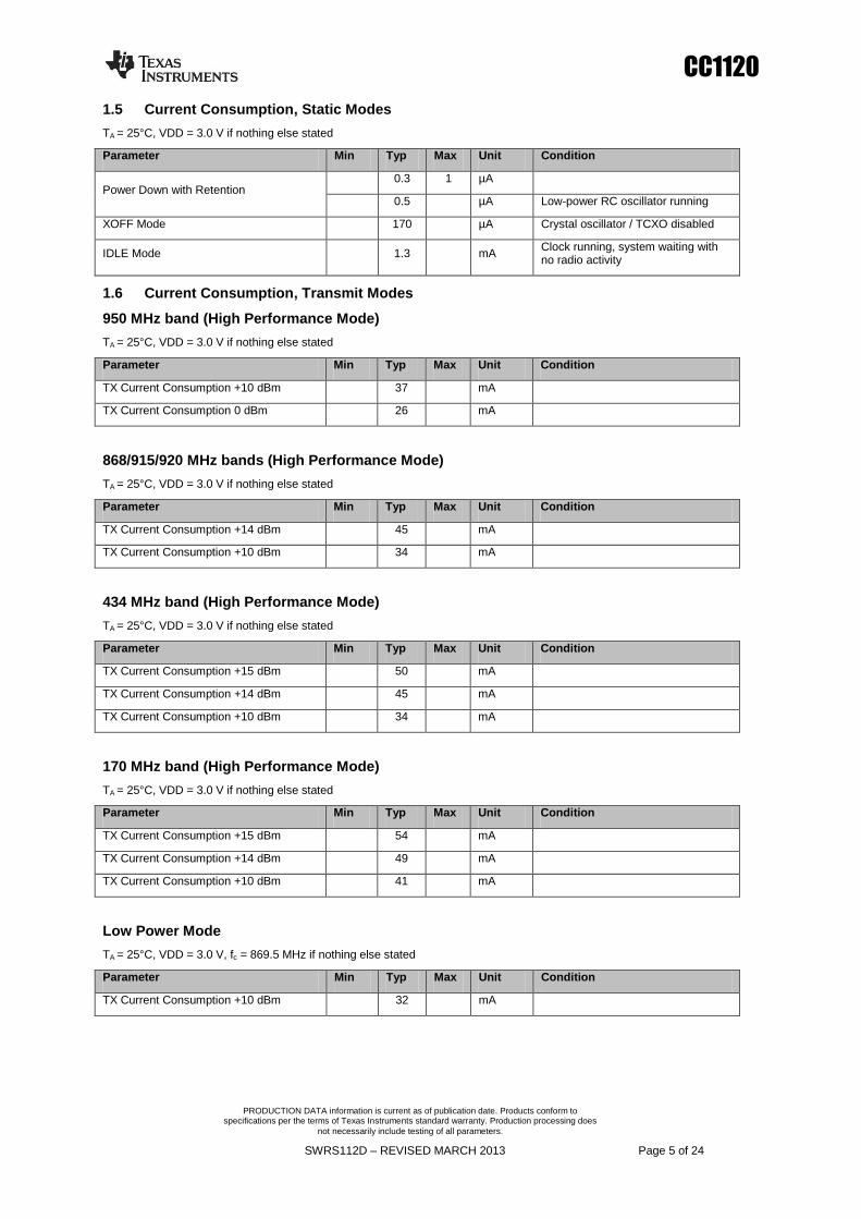
1.5 Current Consumption, Static Modes
TA = 25°C, VDD = 3.0 V if nothing else stated
Parameter Min Typ Max Unit Condition
Power Down with Retention 0.3 1 µA
0.5 µA Low-power RC oscillator running
XOFF Mode 170 µA Crystal oscillator / TCXO disabled
IDLE Mode 1.3 mA Clock running, system waiting with no radio activity
1.6 Current Consumption, Transmit Modes
950 MHz band (High Performance Mode)
TA = 25°C, VDD = 3.0 V if nothing else stated
Parameter Min Typ Max Unit Condition
TX Current Consumption +10 dBm 37 mA
TX Current Consumption 0 dBm 26 mA
868/915/920 MHz bands (High Performance Mode)
TA = 25°C, VDD = 3.0 V if nothing else stated
Parameter Min Typ Max Unit Condition
TX Current Consumption +14 dBm 45 mA
TX Current Consumption +10 dBm 34 mA
434 MHz band (High Performance Mode)
TA = 25°C, VDD = 3.0 V if nothing else stated
Parameter Min Typ Max Unit Condition
TX Current Consumption +15 dBm 50 mA
TX Current Consumption +14 dBm 45 mA
TX Current Consumption +10 dBm 34 mA
170 MHz band (High Performance Mode)
TA = 25°C, VDD = 3.0 V if nothing else stated
Parameter Min Typ Max Unit Condition
TX Current Consumption +15 dBm 54 mA
TX Current Consumption +14 dBm 49 mA
TX Current Consumption +10 dBm 41 mA
Low Power Mode
TA = 25°C, VDD = 3.0 V, fc = 869.5 MHz if nothing else stated
Parameter Min Typ Max Unit Condition
TX Current Consumption +10 dBm 32 mA

CC1120
SWRS112D – REVISED MARCH 2013 Page 6 of 24
PRODUCTION DATA information is current as of publication date. Products conform to specifications per the terms of Texas Instruments standard warranty. Production processing does
not necessarily include testing of all parameters.
1.7 Current Consumption, Receive Modes
High Performance Mode
TA = 25°C, VDD = 3.0 V, fc = 869.5 MHz if nothing else stated
Parameter Min Typ Max Unit Condition
RX Wait for Sync
1.2 kbps, 4 Byte Preamble
38.4kbps, 4 Byte Preamble
2
13.4
mA
mA
Using RX Sniff Mode, where the receiver wakes up at regular intervals to look for an incoming packet
RX Peak Current
433, 868/915/920 and 950 MHz bands
170 MHz band
22
23
mA
mA
Peak current consumption during packet reception at the sensitivity threshold
Average Current Consumption
Check for Data Packet Every 1 Second Using Wake on Radio
15 uA 50 kbps, 5 byte preamble, 32 kHz RC oscillator used as sleep timer
Low Power Mode
TA = 25°C, VDD = 3.0 V, fc = 869.5 MHz if nothing else stated
Parameter Min Typ Max Unit Condition
RX Peak Current Low power RX mode
1.2 kbps
17
mA
Peak current consumption during packet reception at the sensitivity level
1.8 Receive Parameters1
General Receive Parameters (High Performance Mode)
TA = 25°C, VDD = 3.0 V, fc = 869.5 MHz if nothing else stated
Parameter Min Typ Max Unit Condition
Saturation +10 dBm
Digital Channel Filter Programmable Bandwidth
8 200 kHz
IIP3, Normal Mode -14 dBm At maximum gain
IIP3, High Linearity Mode -8 dBm Using 6 dB gain reduction in front end
Datarate Offset Tolerance ±12
±0.2
%
%
With carrier sense detection enabled and assuming 4 byte preamble
With carrier sense detection disabled
Spurious Emissions
1 - 13 GHz (VCO leakage at 3.5 GHz)
30 MHz to 1 GHz
-56
< -57
dBm
dBm
Radiated emissions measured according to ETSI EN 300 220, fc = 869.5 MHz
Optimum Source Impedance
868 / 915 / 920 MHz bands 433 MHz band 169 MHz band
60 + j60 / 30+j30 100 + j60 / 50+ j30 140 + j40 / 70 + j20
Ω Ω Ω
(Differential / Single Ended RX Configurations)
1 All RX measurements made at the antenna connector, to a bit error rate limit of 1%

CC1120
SWRS112D – REVISED MARCH 2013 Page 7 of 24
PRODUCTION DATA information is current as of publication date. Products conform to specifications per the terms of Texas Instruments standard warranty. Production processing does
not necessarily include testing of all parameters.
RX performance in 950 MHz band (High Performance Mode)
TA = 25°C, VDD = 3.0 V if nothing else stated
Parameter Min Typ Max Unit Condition
Sensitivity
Note: Sensitivity can be improved if the TX and RX matching networks are separated.
-120 dBm 1.2 kbps, DEV=4 kHz CHF=10 kHz2
-114 dBm 1.2 kbps, DEV=20 kHz CHF=50 kHz
-107 dBm 50 kbps 2GFSK, DEV=25 kHz, CHF=100 kHz
-100 dBm 200 kbps, DEV=83 kHz (outer symbols), CHF=200 kHz, 4GFSK
3
Blocking and Selectivity
1.2 kbps 2FSK, 12.5 kHz channel separation, 4 kHz deviation, 10 kHz channel filter
51 dB ± 12.5 kHz (adjacent channel)
52 dB ± 25 kHz (alternate channel)
73 dB ± 1 MHz
76 dB ± 2 MHz
81 dB ± 10 MHz
Blocking and Selectivity
1.2 kbps 2FSK, 50 kHz channel separation, 20 kHz deviation, 50 kHz channel filter
47 dB ± 50 kHz (adjacent channel)
48 dB + 100 kHz (alternate channel)
69 dB ± 1 MHz
71 dB ± 2 MHz
78 dB ± 10 MHz
Blocking and Selectivity
50 kbps 2GFSK, 200 kHz channel separation, 25 kHz deviation, 100 kHz channel filter
(Same modulation format as 802.15.4g Mandatory Mode)
43 dB ± 200 kHz (adjacent channel)
51 dB ± 400 kHz (alternate channel)
62 dB ± 1 MHz
65 dB ± 2 MHz
71 dB ± 10 MHz
Blocking and Selectivity
200 kbps 4GFSK, 83 kHz deviation (outer symbols), 200 kHz channel filter, zero IF
37 dB ± 200 kHz (adjacent channel)
44 dB ± 400 kHz (alternate channel)
55 dB ± 1 MHz
58 dB ± 2 MHz
64 dB ± 10 MHz
2 DEV is short for deviation, CHF is short for Channel Filter Bandwidth
3 BT=0.5 is used in all GFSK measurements

CC1120
SWRS112D – REVISED MARCH 2013 Page 8 of 24
PRODUCTION DATA information is current as of publication date. Products conform to specifications per the terms of Texas Instruments standard warranty. Production processing does
not necessarily include testing of all parameters.
RX performance in 868/915/920 MHz bands (High Performance Mode)
TA = 25°C, VDD = 3.0 V if nothing else stated
Parameter Min Typ Max Unit Condition
Sensitivity
-127 dBm
300 bps with coding gain (using a PN spreading sequence with 4 chips per databit) DEV=4 kHz CHF=10 kHz
-123 dBm 1.2 kbps, DEV=4 kHz CHF=10 kHz
-120 dBm 1.2 kbps, DEV=10 kHz CHF=42 kHz
-117 dBm 1.2 kbps, DEV=20 kHz CHF=50 kHz
-114 dBm 4.8 kbps OOK
-110 dBm 38.4 kbps, DEV=20 kHz CHF=100 kHz
-110 dBm 50 kbps 2GFSK, DEV=25 kHz, CHF=100 kHz
-103 dBm 200 kbps, DEV=83 kHz (outer symbols), CHF=200 kHz, 4GFSK
Blocking and Selectivity
1.2 kbps 2FSK, 12.5 kHz channel separation, 4 kHz deviation, 10 kHz channel filter
54 dB ± 12.5 kHz (adjacent channel)
54 dB ± 25 kHz (alternate channel)
75 dB ± 1 MHz
79 dB ± 2 MHz
87 dB ± 10 MHz
Blocking
1.2 kbps 2FSK, 12.5 kHz channel separation, using settings optimized for blocking performance (3 kHz deviation, 7.8 kHz channel filter, minimum loop bandwidth)
78 dB ± 1 MHz
82 dB ± 2 MHz
88 dB ± 8 MHz
88 dB ± 10 MHz
Blocking and Selectivity
1.2 kbps 2FSK, 50 kHz channel separation, 20 kHz deviation, 50 kHz channel filter
48 dB ± 50 kHz (adjacent channel)
48 dB + 100 kHz (alternate channel)
69 dB ± 1 MHz
74 dB ± 2 MHz
81 dB ± 10 MHz
Blocking and Selectivity
38.4 kbps 2GFSK, 100 kHz channel separation, 20 kHz deviation, 100 kHz channel filter
42 dB + 100 kHz (adjacent channel)
43 dB ± 200 kHz (alternate channel)
62 dB ± 1 MHz
66 dB ± 2 MHz
74 dB ± 10 MHz

CC1120
SWRS112D – REVISED MARCH 2013 Page 9 of 24
PRODUCTION DATA information is current as of publication date. Products conform to specifications per the terms of Texas Instruments standard warranty. Production processing does
not necessarily include testing of all parameters.
RX performance in 868/915/920 MHz bands (continued from previous page)
Parameter Min Typ Max Unit Condition
Blocking and Selectivity
50 kbps 2GFSK, 200 kHz channel separation, 25 kHz deviation, 100 kHz channel filter
(Same modulation format as 802.15.4g Mandatory Mode)
43 dB ± 200 kHz (adjacent channel)
50 dB ± 400 kHz (alternate channel)
61 dB ± 1 MHz
65 dB ± 2 MHz
74 dB ± 10 MHz
Blocking and Selectivity
200 kbps 4GFSK, 83 kHz deviation (outer symbols), 200 kHz channel filter, zero IF
36 dB ± 200 kHz (adjacent channel)
44 dB ± 400 kHz (alternate channel)
55 dB ± 1 MHz
59 dB ± 2 MHz
67 dB ± 10 MHz
Image Rejection
(Image compensation enabled) 54 dB
1.2 kbps, DEV=4 kHz CHF=10 kHz, image at -125 kHz
RX performance in 434 MHz band (High Performance Mode)
TA = 25°C, VDD = 3.0 V if nothing else stated
Parameter Min Typ Max Unit Condition
Sensitivity
-123 dBm 1.2 kbps, DEV=4 kHz CHF=10 kHz
-109 dBm 50 kbps 2GFSK, DEV=25 kHz, CHF=100 kHz
-116 dBm 1.2 kbps, DEV=20 kHz CHF=50 kHz
Blocking and Selectivity
1.2 kbps 2FSK, 12.5 kHz channel separation, 4 kHz deviation, 10 kHz channel filter
60 dB ± 12.5 kHz (adjacent channel)
60 dB ± 25 kHz (alternate channel)
79 dB ± 1 MHz
82 dB ± 2 MHz
91 dB ± 10 MHz
Blocking and Selectivity
1.2 kbps 2FSK, 50 kHz channel separation, 20 kHz deviation, 50 kHz channel filter
54 dB ± 50 kHz (adjacent channel)
54 dB + 100 kHz (alternate channel)
74 dB ± 1 MHz
78 dB ± 2 MHz
86 dB ± 10 MHz
Blocking and Selectivity
38.4 kbps 2GFSK, 100 kHz channel separation, 20 kHz deviation, 100 kHz channel filter
47 dB + 100 kHz (adjacent channel)
50 dB ± 200 kHz (alternate channel)
67 dB ± 1 MHz
71 dB ± 2 MHz
78 dB ± 10 MHz
CC1120
SWRS112D – REVISED MARCH 2013 Page 10 of 24
PRODUCTION DATA information is current as of publication date. Products conform to specifications per the terms of Texas Instruments standard warranty. Production processing does
not necessarily include testing of all parameters.
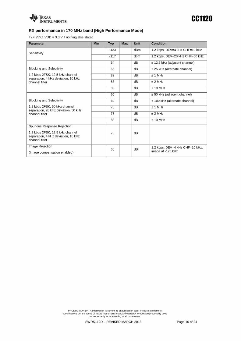
RX performance in 170 MHz band (High Performance Mode)
TA = 25°C, VDD = 3.0 V if nothing else stated
Parameter Min Typ Max Unit Condition
Sensitivity -123 dBm 1.2 kbps, DEV=4 kHz CHF=10 kHz
-117 dbm 1.2 kbps, DEV=20 kHz CHF=50 kHz
Blocking and Selectivity
1.2 kbps 2FSK, 12.5 kHz channel separation, 4 kHz deviation, 10 kHz channel filter
64 dB ± 12.5 kHz (adjacent channel)
66 dB ± 25 kHz (alternate channel)
82 dB ± 1 MHz
83 dB ± 2 MHz
89 dB ± 10 MHz
Blocking and Selectivity
1.2 kbps 2FSK, 50 kHz channel separation, 20 kHz deviation, 50 kHz channel filter
60 dB ± 50 kHz (adjacent channel)
60 dB + 100 kHz (alternate channel)
76 dB ± 1 MHz
77 dB ± 2 MHz
83 dB ± 10 MHz
Spurious Response Rejection
1.2 kbps 2FSK, 12.5 kHz channel separation, 4 kHz deviation, 10 kHz channel filter
70 dB
Image Rejection
(Image compensation enabled) 66 dB
1.2 kbps, DEV=4 kHz CHF=10 kHz, image at -125 kHz

CC1120
SWRS112D – REVISED MARCH 2013 Page 11 of 24
PRODUCTION DATA information is current as of publication date. Products conform to specifications per the terms of Texas Instruments standard warranty. Production processing does
not necessarily include testing of all parameters.
RX performance in Low Power Mode
TA = 25°C, VDD = 3.0 V, fc = 869.5 MHz if nothing else stated
Parameter Min Typ Max Unit Condition
Sensitivity
-111 dBm 1.2 kbps, DEV=4 kHz CHF=10 kHz
-99 dBm 38.4 kbps, DEV=50 kHz CHF=100 kHz
-99 dBm 50 kbps 2GFSK, DEV=25 kHz, CHF=100 kHz
Blocking and Selectivity
1.2 kbps 2FSK, 12.5 kHz channel separation, 4 kHz deviation, 10 kHz channel filter
46 dB ± 12.5 kHz (adjacent channel)
46 dB ± 25 kHz (alternate channel)
73 dB ± 1 MHz
78 dB ± 2 MHz
79 dB ± 10 MHz
Blocking and Selectivity
1.2 kbps 2FSK, 50 kHz channel separation, 20 kHz deviation, 50 kHz channel filter
43 dB ± 50 kHz (adjacent channel)
45 dB + 100 kHz (alternate channel)
71 dB ± 1 MHz
74 dB ± 2 MHz
75 dB ± 10 MHz
Blocking and Selectivity
38.4 kbps 2GFSK, 100 kHz channel separation, 20 kHz deviation, 100 kHz channel filter
37 dB + 100 kHz (adjacent channel)
43 dB + 200 kHz (alternate channel)
58 dB ± 1 MHz
62 dB ± 2 MHz
64 dB + 10 MHz
Blocking and Selectivity
50 kbps 2GFSK, 200 kHz channel separation, 25 kHz deviation, 100 kHz channel filter
(Same modulation format as 802.15.4g Mandatory Mode)
43 dB + 200 kHz (adjacent channel)
52 dB + 400 kHz (alternate channel)
60 dB ± 1 MHz
64 dB ± 2 MHz
65 dB ± 10 MHz
Saturation +10 dBm
CC1120
SWRS112D – REVISED MARCH 2013 Page 12 of 24
PRODUCTION DATA information is current as of publication date. Products conform to specifications per the terms of Texas Instruments standard warranty. Production processing does
not necessarily include testing of all parameters.
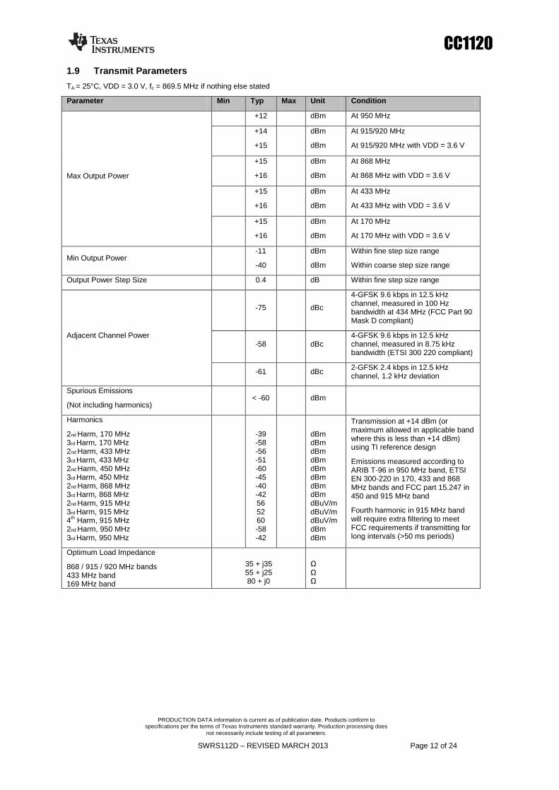
1.9 Transmit Parameters
TA = 25°C, VDD = 3.0 V, fc = 869.5 MHz if nothing else stated
Parameter Min Typ Max Unit Condition
Max Output Power
+12 dBm At 950 MHz
+14
+15
dBm
dBm
At 915/920 MHz
At 915/920 MHz with VDD = 3.6 V
+15
+16
dBm
dBm
At 868 MHz
At 868 MHz with VDD = 3.6 V
+15
+16
dBm
dBm
At 433 MHz
At 433 MHz with VDD = 3.6 V
+15
+16
dBm
dBm
At 170 MHz
At 170 MHz with VDD = 3.6 V
Min Output Power -11
-40
dBm
dBm
Within fine step size range
Within coarse step size range
Output Power Step Size 0.4 dB Within fine step size range
Adjacent Channel Power
-75 dBc
4-GFSK 9.6 kbps in 12.5 kHz channel, measured in 100 Hz bandwidth at 434 MHz (FCC Part 90 Mask D compliant)
-58 dBc 4-GFSK 9.6 kbps in 12.5 kHz channel, measured in 8.75 kHz bandwidth (ETSI 300 220 compliant)
-61 dBc 2-GFSK 2.4 kbps in 12.5 kHz channel, 1.2 kHz deviation
Spurious Emissions
(Not including harmonics) < -60 dBm
Harmonics
2nd Harm, 170 MHz 3rd Harm, 170 MHz 2nd Harm, 433 MHz 3rd Harm, 433 MHz 2nd Harm, 450 MHz 3rd Harm, 450 MHz 2nd Harm, 868 MHz 3rd Harm, 868 MHz 2nd Harm, 915 MHz 3rd Harm, 915 MHz 4
th Harm, 915 MHz
2nd Harm, 950 MHz 3rd Harm, 950 MHz
-39 -58 -56 -51 -60 -45 -40 -42 56 52 60 -58 -42
dBm dBm dBm dBm dBm dBm dBm dBm dBuV/m dBuV/m dBuV/m dBm dBm
Transmission at +14 dBm (or maximum allowed in applicable band where this is less than +14 dBm) using TI reference design
Emissions measured according to ARIB T-96 in 950 MHz band, ETSI EN 300-220 in 170, 433 and 868 MHz bands and FCC part 15.247 in 450 and 915 MHz band
Fourth harmonic in 915 MHz band will require extra filtering to meet FCC requirements if transmitting for long intervals (>50 ms periods)
Optimum Load Impedance
868 / 915 / 920 MHz bands 433 MHz band 169 MHz band
35 + j35 55 + j25 80 + j0
Ω Ω Ω

CC1120
SWRS112D – REVISED MARCH 2013 Page 13 of 24
PRODUCTION DATA information is current as of publication date. Products conform to specifications per the terms of Texas Instruments standard warranty. Production processing does
not necessarily include testing of all parameters.
1.10 PLL Parameters
High Performance Mode
TA = 25°C, VDD = 3.0 V, fc = 869.5 MHz if nothing else stated
Parameter Min Typ Max Unit Condition
Phase Noise in 950 MHz Band
-99 dBc/Hz ± 10 kHz offset
-99 dBc/Hz ± 100 kHz offset
-123 dBc/Hz ± 1 MHz offset
Phase Noise in 868/915/920 MHz Bands
-99 dBc/Hz ± 10 kHz offset
-100 dBc/Hz ± 100 kHz offset
-122 dBc/Hz ± 1 MHz offset
Phase Noise in 433 MHz Band
-106 dBc/Hz ± 10 kHz offset
-107 dBc/Hz ± 100 kHz offset
-127 dBc/Hz ± 1 MHz offset
Phase Noise in 170 MHz Band
-111 dBc/Hz ± 10 kHz offset
-116 dBc/Hz ± 100 kHz offset
-135 dBc/Hz ± 1 MHz offset
Low Power Mode
TA = 25°C, VDD = 3.0 V, fc = 869.5 MHz if nothing else stated
Parameter Min Typ Max Unit Condition
Phase Noise in 950 MHz Band
-90 dBc/Hz ± 10 kHz offset
-92 dBc/Hz ± 100 kHz offset
-124 dBc/Hz ± 1 MHz offset
Phase Noise in 868/915/920 MHz Bands
-95 dBc/Hz ± 10 kHz offset
-95 dBc/Hz ± 100 kHz offset
-124 dBc/Hz ± 1 MHz offset
Phase Noise in 433 MHz Band
-98 dBc/Hz ± 10 kHz offset
-102 dBc/Hz ± 100 kHz offset
-129 dBc/Hz ± 1 MHz offset
Phase Noise in 170 MHz Band
-106 dBc/Hz ± 10 kHz offset
-110 dBc/Hz ± 100 kHz offset
-136 dBc/Hz ± 1 MHz offset

CC1120
SWRS112D – REVISED MARCH 2013 Page 14 of 24
PRODUCTION DATA information is current as of publication date. Products conform to specifications per the terms of Texas Instruments standard warranty. Production processing does
not necessarily include testing of all parameters.
1.11 Wake-up and Timing
TA = 25°C, VDD = 3.0 V, fc = 869.5 MHz if nothing else stated
Parameter Min Typ Max Unit Condition
Powerdown to IDLE 0.4 ms Depends on crystal
IDLE to RX/TX 166 µs Calibration disabled
461 µs Calibration enabled
RX/TX Turnaround 50 µs
RX/TX to IDLE time
296 µs Calibrate when leaving RX/TX enabled
0 µs Calibrate when leaving RX/TX disabled
Frequency Synthesizer Calibration 0.4 ms When using SCAL strobe
Minimum Required Number of Preamble Bytes
0.5 bytes
Required for RF front end gain settling only. Digital demodulation does not require preamble for settling
Time From Start RX Until Valid RSSI
Including gain settling (function of channel bandwidth. Programmable for trade-off between speed and accuracy)
4.6 ms 12.5 kHz channels
0.3 ms 200 kHz channels
1.12 32 MHz Crystal Oscillator
TA = 25°C, VDD = 3.0 V if nothing else stated
Parameter Min Typ Max Unit Condition
Crystal Frequency 32 33.6 MHz
Note: It is recommended that the crystal frequency is chosen so that the RF channel(s) are >1 MHz away from multiples of XOSC in TX and XOSC/2 in RX
Load Capacitance (CL) 10 pF
ESR 60 Ω Simulated over operating conditions
Start-up Time 0.4 ms Depends on crystal
1.13 32 MHz Clock Input (TCXO)
TA = 25°C, VDD = 3.0 V if nothing else stated
Parameter Min Typ Max Unit Condition
Clock Frequency 32 33.6 MHz
Clock input amplitude (peak-to-peak) 0.8 VDD V Simulated over operating conditions

CC1120
SWRS112D – REVISED MARCH 2013 Page 15 of 24
PRODUCTION DATA information is current as of publication date. Products conform to specifications per the terms of Texas Instruments standard warranty. Production processing does
not necessarily include testing of all parameters.
1.14 32 kHz Clock Input
TA = 25°C, VDD = 3.0 V if nothing else stated
Parameter Min Typ Max Unit Condition
Clock Frequency 32 kHz
32 kHz Clock Input Pin Input High Voltage 0.8×VDD V
32 kHz Clock Input Pin Input Low Voltage 0.2×VDD V
1.15 32 kHz RC Oscillator
TA = 25°C, VDD = 3.0 V if nothing else stated.
Parameter Min Typ Max Unit Condition
Frequency 32 kHz After Calibration
Frequency Accuracy After Calibration ±0.1 % Relative to frequency reference (i.e. 32 MHz crystal or TCXO)
Initial Calibration Time 1.6 ms
1.16 I/O and Reset
TA = 25°C, VDD = 3.0 V if nothing else stated
Parameter Min Typ Max Unit Condition
Logic Input High Voltage
Logic Input Low Voltage
0.8×VDD
0.2×VDD
V
V
Logic Output High Voltage
Logic Output Low Voltage
0.8×VDD
0.2×VDD
V
V At 4 mA output load or less
Power-on Reset Threshold 1.3 V Voltage on DVDD pin
1.17 Temperature Sensor
TA = 25°C, VDD = 3.0 V if nothing else stated
Parameter Min Typ Max Unit Condition
Temperature Sensor Range -40 85 °C
Temperature Coefficient 2.66 mV / °C Change in sensor output voltage vs change in temperature
Typical Output Voltage 794 mV Typical sensor output voltage at TA = 25°C, VDD = 3.0 V
VDD Coefficient 1.17 mV / V Change in sensor output voltage vs change in VDD
The CC1120 can be configured to provide a voltage proportional to temperature on GPIO1. Using the information above, the temperature can be estimated by measuring this voltage. Please refer to the CC1120 user guide for more information.

CC1120
SWRS112D – REVISED MARCH 2013 Page 16 of 24
PRODUCTION DATA information is current as of publication date. Products conform to specifications per the terms of Texas Instruments standard warranty. Production processing does
not necessarily include testing of all parameters.
2 Typical Performance Curves
TA = 25°C, VDD = 3.0 V, fc = 869.5 MHz if nothing else stated All measurements performed on CC1120EM_868_915 rev.1.0.1, CC1120EM_955 rev.1.2.1, CC1120EM_420_470 rev.1.0.1 or CC1120EM_169 rev.1.2 Note that the "output power vs load impedance" plot was measured at the 50 Ω antenna connector
Sensitivity vs Temperature
1.2kbps, 4kHz deviation, 10kHz ch. filter bw
-125
-124
-123
-122
-121
-120
-40 0 40 80
Temperature (ºC)
Sensitiv
ity (
dB
m)
Sync Word Sensitivity vs Sync Word Detect Threshold
1.2kbps, 4kHz deviation, 10kHz ch. filter bw
-130
-128
-126
-124
-122
-120
-118
-116
-114
3 5 7 9 11 13 15 17
Sync Word Detect Threshold
Sensitiv
ity (
dB
m)
RX Current vs Input Level
1.2kbps, 4kHz deviation, 10kHz ch. filter bw
20.8
21.2
21.6
22
22.4
22.8
23.2
-130 -80 -30 20
Input Level (dBm)
RX
Curr
ent (m
A)
Selectivity vs offset frequency (12.5kHz channels)
1.2kbps, 4kHz deviation, 10kHz ch. filter bw
-20
-10
0
10
20
30
40
50
60
70
169.9 169.95 170 170.05 170.1
Frequency (MHz)
Sele
ctivity (
dB
)
Selectivity vs offset frequency (12.5kHz channels)
1.2kbps, 4kHz deviation, 10kHz ch. filter bw
-10
0
10
20
30
40
50
60
70
859.9 859.95 860 860.05 860.1
Frequency (MHz)
Sele
ctivity (
dB
)
Sensitivity vs Voltage
1.2kbps, 4kHz deviation, 10kHz ch. filter bw
-124
-123
-122
-121
-120
2 2.5 3 3.5
Supply Voltage (V)
Sensitiv
ity (
dB
m)

CC1120
SWRS112D – REVISED MARCH 2013 Page 17 of 24
PRODUCTION DATA information is current as of publication date. Products conform to specifications per the terms of Texas Instruments standard warranty. Production processing does
not necessarily include testing of all parameters.
Output Power at 868MHz
vs PA power setting
-50
-40
-30
-20
-10
0
10
20
7F 7B 77 73 6F 6B 67 63 5F 5B 57 53 4F 4B 47 43
PA power setting
Ou
tput
Pow
er
(dB
m)
TX Current at 868MHz
vs PA power setting
0
10
20
30
40
50
60
7F 7B 77 73 6F 6B 67 63 5F 5B 57 53 4F 4B 47 43
PA power setting
TX
Cu
rren
t (m
A)
RSSI vs Input Level
1.2kbps, 4kHz deviation, 10kHz ch. filter bw
-40
-20
0
20
40
60
80
100
-150 -100 -50 0
Input Level (dBm)
RS
SI
Output Power vs Voltage
Max Setting, 170 MHz
6
8
10
12
14
16
18
2 2.5 3 3.5
Supply Voltage (V)
Outp
ut P
ow
er
(dB
m)
Output Power vs Temperature
Max Setting, 170 MHz, 3.6V
15
15.5
16
16.5
17
-40 0 40 80
Temperature (ºC)
Outp
ut P
ow
er
(dB
m)

CC1120
SWRS112D – REVISED MARCH 2013 Page 18 of 24
PRODUCTION DATA information is current as of publication date. Products conform to specifications per the terms of Texas Instruments standard warranty. Production processing does
not necessarily include testing of all parameters.
GPIO Output Low Voltage vs Current Being Sinked
0
200
400
600
800
1000
1200
1400
0 5 10 15 20 25 30 35
Current (mA)
GP
IO O
utp
ut L
ow
Vo
lta
ge
(m
V)
GPIO Output High Voltage vs Current Being Sourced
1.5
1.7
1.9
2.1
2.3
2.5
2.7
2.9
3.1
0 5 10 15 20 25 30 35
Current (mA)
GP
IO O
utp
ut h
igh
Vo
lta
ge
(V
)

CC1120
SWRS112D – REVISED MARCH 2013 Page 19 of 24
PRODUCTION DATA information is current as of publication date. Products conform to specifications per the terms of Texas Instruments standard warranty. Production processing does
not necessarily include testing of all parameters.
3 Pin Configuration
The CC1120 pin-out is shown in the table below.
Pin # Pin name Type / direction Description
1 VDD_GUARD Power 2.0 - 3.6 V VDD
2 RESET_N Digital Input Asynchronous, active-low digital reset
3 GPIO3 Digital Input/Output General purpose IO
4 GPIO2 Digital Input/Output General purpose IO
5 DVDD Power 2.0 - 3.6 VDD to internal digital regulator
6 DCPL Power Digital regulator output to external decoupling capacitor
7 SI Digital Input Serial data in
8 SCLK Digital Input Serial data clock
9 SO(GPIO1) Digital Input/Output Serial data out (General purpose IO)
10 GPIO0 Digital Input/Output General purpose IO
11 CSn Digital Input Active-low chip-select
12 DVDD Power 2.0 - 3.6 V VDD
13 AVDD_IF Power 2.0 - 3.6 V VDD
14 RBIAS Analog External high precision R
15 AVDD_RF Power 2.0 - 3.6 V VDD
16 NC Not connected
17 PA Analog Single-ended TX output
18 TRX_SW Analog TX/RX switch
19 LNA_P Analog Differential RX input
20 LNA_N Analog Differential RX input
21 DCPL_VCO Power Pin for external decoupling of VCO supply regulator
22 AVDD_SYNTH1 Power 2.0 - 3.6 V VDD
23 LPF0 Analog External loopfilter components
24 LPF1 Analog External loopfilter components
25 AVDD_PFD_CHP Power 2.0 - 3.6 V VDD
26 DCPL_PFD_CHP Power Pin for external decoupling of PFD and CHP regulator
27 AVDD_SYNTH2 Power 2.0 - 3.6 V VDD
28 AVDD_XOSC Power 2.0 - 3.6 V VDD
29 DCPL_XOSC Power Pin for external decoupling of XOSC supply regulator
30 XOSC_Q1 Analog Crystal oscillator pin 1 (must be grounded if a TCXO or other external clock connected to EXT_XOSC is used)
31 XOSC_Q2 Analog Crystal oscillator pin 2 (must be left floating if a TCXO or other external clock connected to EXT_XOSC is used)
32 EXT_XOSC Digital Input Pin for external XOSC input (must be grounded if a regular XOSC connected to XOSC_Q1 and XOSC_Q2 is used)
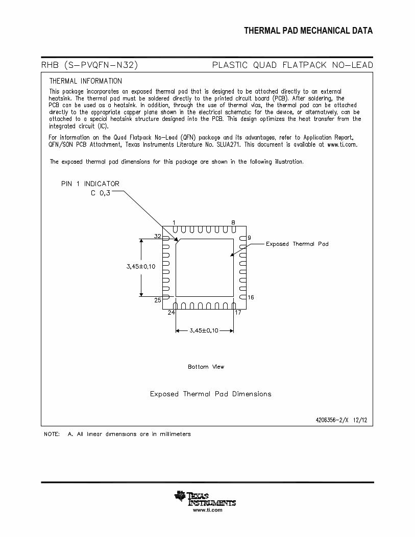
- GND Ground Pad The ground pad must be connected to a solid ground plane

CC1120
SWRS112D – REVISED MARCH 2013 Page 20 of 24
PRODUCTION DATA information is current as of publication date. Products conform to specifications per the terms of Texas Instruments standard warranty. Production processing does
not necessarily include testing of all parameters.
4 Block Diagram
A system block diagram of CC1120 is shown Figure 4.1.
CC112X
MARC
Main Radio Control Unit
Ultra low power 16 bit
MCU
256 byte
FIFO RAM
buffer
4k byte
ROM
RF and DSP frontend
Packet handler
and FIFO controlConfiguration and
status registers
eWOR
Enhanced ultra low power
Wake On Radio timer
SPI
Serial configuration
and data interface
Interrupt and
IO handlerSystem bus
PA
LNA_P
LNA_N
90dB dynamic
range ADC
90dB dynamic
range ADC
High linearity
LNA
14dBm high
efficiency PA
Ch
an
ne
l
filte
r
XOSC
Co
rdic
AGC
Automatic Gain Control, 60dB VGA range
RSSI measurements and carrier sense detection
Highly flexible FSK / OOK
demodulator
(optional bit clock)
(optional low jitter serial
data output for legacy
protocols)
Data interface with
signal chain access
XOSC_Q1
XOSC_Q2
Ultra low power 32kHz
auto-calibrated RC oscillator(optional 32kHz
clock intput)
CSn (chip select)
SI (serial input)
SO (serial output)
SCLK (serial clock)
(optional GPIO0-3)
Mo
du
lato
r
Fully integrated Fractional-N
Frequency Synthesizer
Output power ramping and OOK / ASK modulation
ifamp
ifamp
(optional autodetected
external XOSC / TCXO)
(optional GPIO for
antenna diversity)
I
Q
Battery sensor /
temp sensor
Power on reset
Figure 4.1 : System Block Diagram
4.1 Frequency Synthesizer
At the heart of CC1120 there is a fully integrated, fractional-N, ultra high performance frequency synthesizer. The frequency synthesizer is designed for excellent phase noise performance, providing very high selectivity and blocking performance. The system is designed to comply with the most stringent regulatory spectral masks at maximum transmit power.
Either a crystal can be connected to XOSC_Q1 and XOSC_Q2, or a TCXO can be connected to the EXT_XOSC input. The oscillator generates the reference frequency for the synthesizer, as well as clocks for the ADC and the digital part. To reduce system cost, CC1120 has high accuracy frequency estimation and compensation registers to measure and compensate for crystal inaccuracies, enabling the use of lower cost crystals. If a TCXO is used, the CC1120 will automatically turn the TCXO on and off when needed to support low power modes and Wake-On-Radio operation.
4.2 Receiver
CC1120 features a highly flexible receiver. The received RF signal is amplified by the low-noise amplifier (LNA) and down-converted in quadrature (I and Q) to the intermediate frequency (IF). At IF, the I/Q signals are digitized by the high dynamic range ADCs.
An advanced Automatic Gain Control (AGC) unit adjusts the front end gain, and enables the CC1120 to receive both strong and weak signals, even in the presence of strong interferers. High attenuation channel and data filtering enable reception with strong neighbor channel interferers. The I/Q signal is converted to a phase / magnitude signal to support both FSK and OOK modulation schemes.

CC1120
SWRS112D – REVISED MARCH 2013 Page 21 of 24
PRODUCTION DATA information is current as of publication date. Products conform to specifications per the terms of Texas Instruments standard warranty. Production processing does
not necessarily include testing of all parameters.
A sophisticated pattern recognition algorithm locks onto the synchronization word without need for preamble settling bytes. Receiver settling time is therefore reduced to the settling time of the AGC, typically 4 bits. The advanced pattern recognition also greatly reduces the problem of false sync triggering on noise, further reducing power consumption and improving sensitivity and reliability. The pattern recognition logic can also be used as a high performance preamble detector to reliably detect a valid preamble in the channel.
A novel I/Q compensation algorithm removes any problem of I/Q mismatch and hence avoids time consuming and costly I/Q / image calibration steps in production or in the field.
4.3 Transmitter
The CC1120 transmitter is based on direct synthesis of the RF frequency (in-loop modulation). To achieve effective spectrum usage, CC1120 has extensive data filtering and shaping in TX to support high throughput data communication in narrowband channels. The modulator also controls power ramping to remove issues such as spectral splattering when driving external high power RF amplifiers.
4.4 Radio Control and User Interface
The CC1120 digital control system is built around MARC (Main Radio Control) implemented using an internal high performance 16 bit ultra low power processor. MARC handles power modes, radio sequencing and protocol timing.
A 4-wire SPI serial interface is used for configuration and data buffer access. The digital baseband includes support for channel configuration, packet handling, and data buffering. The host MCU can stay in power down until a valid RF packet has been received, and then burst read the data, greatly reducing the power consumption and computing power required from the host MCU.
The CC1120 radio control and user interface is based on the widely used CC1101 transceiver to enable easy SW transition between the two platforms. The command strobes and the main radio states are the same for the two platforms.
For legacy formats CC1120 also has support for two serial modes. In synchronous serial mode CC1120 performs bit synchronization and provides the MCU with a bit clock with associated data. In transparent mode CC1120 outputs the digital baseband signal using a digital interpolation filter to eliminate jitter introduced by digital filtering and demodulation.
4.5 Enhanced Wake-On-Radio (eWOR)
eWOR, using a flexible integrated sleep timer, enables automatic receiver polling with no intervention from the MCU. The CC1120 will enter RX, listen and return to sleep if a valid RF packet is not received. The sleep interval and duty cycle can be configured to make a trade-off between network latency and power consumption. Incoming messages are time-stamped to simplify timer re-synchronization.
The eWOR timer runs off an ultra low power 32 kHz RC oscillator. To improve timing accuracy, the RC oscillator can be automatically calibrated to the RF crystal in configurable intervals.
4.6 Sniff Mode
The CC1120 supports very quick start up times, and requires very few preamble bits. Sniff Mode uses this to dramatically reduce the current consumption while the receiver is waiting for data.
Since the CC1120 is able to wake up and settle much faster than the length of most preambles, it is not required to be in RX continuously while waiting for a packet to arrive. Instead, the enhanced wake-on-radio feature can be used to put the device into sleep periodically. By setting an appropriate sleep time, the CC1120 will be able to wake up and receive the packet when it arrives with no performance loss. This removes the need for accurate timing synchronization between
CC1120
SWRS112D – REVISED MARCH 2013 Page 22 of 24
PRODUCTION DATA information is current as of publication date. Products conform to specifications per the terms of Texas Instruments standard warranty. Production processing does
not necessarily include testing of all parameters.
transmitter and receiver, and allows the user to trade off current consumption between the transmitter and receiver.
4.7 Antenna Diversity
Antenna diversity can increase performance in a multi-path environment. An external antenna switch is required. The switch can be automatically controlled by CC1120 using one of the GPIO pins (also support for differential output control signal typically used in RF switches).
If antenna diversity is enabled, the GPIO will alternate between states until a valid RF input signal is detected. An optional acknowledge packet can be transmitted without changing GPIO state.
An incoming RF signal can be validated by received signal strength, by using the automatic preamble detector, or a combination of the two. Using the preamble detector will make a more robust system and avoid the need to set a defined signal strength threshold, as this threshold will set the sensitivity limit of the system.
CC1120
SWRS112D – REVISED MARCH 2013 Page 23 of 24
PRODUCTION DATA information is current as of publication date. Products conform to specifications per the terms of Texas Instruments standard warranty. Production processing does
not necessarily include testing of all parameters.
5 Typical Application Circuit
Very few external components are required for the operation of CC1120. A typical application circuit is shown below. Note that it does not show how the board layout should be done, which will greatly influence the RF performance of CC1120.
This section is meant as an introduction only. Note that decoupling capacitors for power pins are not shown in the figure below.
(optional control pin
from CC1120)
AV
DD
_P
FD
_C
HP
XO
SC
_Q
2
XO
SC
_Q
1
DC
PL
_P
FD
_C
HP
AV
DD
_S
YN
TH
2
DC
PL
_X
OS
C
AV
DD
_X
OS
C
EX
T_
XO
SC
RESET_N
GPIO3
GPIO2
DVDD
VDD_GUARD
DCPL
SI
SCLK
CS
n
SO
(G
PIO
1)
DV
DD
RB
IAS
AV
DD
_IF
AV
DD
_R
F
N.C
.
GP
IO0
LNA_P
LNA_N
DCPL_VCO
AVDD_SYNTH1
PA
TRX_SW
LPF0
LPF1vddv
dd
vd
dvdd
vd
d
CC11205
4
3
2
1
6
7
8
13
12
11
109
14
15
16
20
21
22
23
24
19
18
17
28
29
30
31
32
27
26
25
vdd
vd
d
32 MHz
crystal
Optional
XOSC/
TCXO
MCU connection
SPI interface and
optional gpio pins
vd
d
vd
d
vd
d
Figure 5.1 : Typical Application Circuit

CC1120
SWRS112D – REVISED MARCH 2013 Page 24 of 24
PRODUCTION DATA information is current as of publication date. Products conform to specifications per the terms of Texas Instruments standard warranty. Production processing does
not necessarily include testing of all parameters.
6 History
Revision Date Description / Changes
SWRS112D March 2013 Added ARIB T-108 to list of regulations
Added 1.2 kbps using 10 kHz deviation and 41.7 kHz channel filter
Added optimum source / load impedance
Added missing unit "dBm" in output power section
Added information about the temperature sensor
Clarified how the typical performance curves have been measured
Corrected wrong deviation for 38.4 kbps sensitivity (was 50 kHz, corrected to 20 kHz)
Pin CS_N renamed to CSn to comply with naming convention used in the user guide
Updated modulation format information in image rejection sections
Stated which ETSI EN 300 220 receiver category that is suitable for low power mode
Added deviation and channel filter bandwidth for 300 bps format
Added blocking data using settings optimized for best blocking performance at 868/915/920 MHz
Clarified under max ratings that I/O voltages should not exceed device supply voltage by more than 0.3 V
Various minor spelling errors corrected
SWRS112C April 2012 Added ground pad on page 1 pin-out and pin description
Added TCXO clock input voltage requirement
Changed all pin names in pin description and figures to UPPERCASE
Changed "PA OUT" to "PA" in block diagram
Corrected deviation on 38.4kbps case from 50kHz to 20kHz
Corrected error in EM list: CC1120EM_420_970 is corrected to CC1120EM_420_470
Added 274 - 320 MHz band and pointed to app note for more info (added mention of 315 MHz band on front page)
Updated sniff mode current to 2 mA
Added "WaveMatch:" in front of "Advanced digital signal processing ..." on front page
Data rate offset tolerance: specified that 4 byte preamble only applies to 12% offset
Removed solder reflow temperature and moisture sensitivity level under absolute max ratings
Moved crystal ESR to ‘max’ column
Added History section
SWRS112B Sept. 2011 Initial release
SWRS112 Aug. 2011 Preliminary Data Sheet

PACKAGE OPTION ADDENDUM
www.ti.com 13-May-2013
Addendum-Page 1
PACKAGING INFORMATION
Orderable Device Status(1)
Package Type PackageDrawing
Pins PackageQty
Eco Plan(2)
Lead/Ball Finish MSL Peak Temp(3)
Op Temp (°C) Top-Side Markings(4)
Samples
CC1120RHBR ACTIVE QFN RHB 32 3000 Green (RoHS& no Sb/Br)
CU NIPDAUAG Level-3-260C-168 HR -40 to 85 CC1120
CC1120RHBT ACTIVE QFN RHB 32 250 Green (RoHS& no Sb/Br)
CU NIPDAUAG Level-3-260C-168 HR -40 to 85 CC1120
CC1120RHMR NRND QFN RHM 32 3000 Green (RoHS& no Sb/Br)
CU NIPDAU Level-3-260C-168 HR -40 to 85 CC1120
CC1120RHMT NRND QFN RHM 32 250 Green (RoHS& no Sb/Br)
CU NIPDAU Level-3-260C-168 HR -40 to 85 CC1120
(1) The marketing status values are defined as follows:ACTIVE: Product device recommended for new designs.LIFEBUY: TI has announced that the device will be discontinued, and a lifetime-buy period is in effect.NRND: Not recommended for new designs. Device is in production to support existing customers, but TI does not recommend using this part in a new design.PREVIEW: Device has been announced but is not in production. Samples may or may not be available.OBSOLETE: TI has discontinued the production of the device.
(2) Eco Plan - The planned eco-friendly classification: Pb-Free (RoHS), Pb-Free (RoHS Exempt), or Green (RoHS & no Sb/Br) - please check http://www.ti.com/productcontent for the latest availabilityinformation and additional product content details.TBD: The Pb-Free/Green conversion plan has not been defined.Pb-Free (RoHS): TI's terms "Lead-Free" or "Pb-Free" mean semiconductor products that are compatible with the current RoHS requirements for all 6 substances, including the requirement thatlead not exceed 0.1% by weight in homogeneous materials. Where designed to be soldered at high temperatures, TI Pb-Free products are suitable for use in specified lead-free processes.Pb-Free (RoHS Exempt): This component has a RoHS exemption for either 1) lead-based flip-chip solder bumps used between the die and package, or 2) lead-based die adhesive used betweenthe die and leadframe. The component is otherwise considered Pb-Free (RoHS compatible) as defined above.Green (RoHS & no Sb/Br): TI defines "Green" to mean Pb-Free (RoHS compatible), and free of Bromine (Br) and Antimony (Sb) based flame retardants (Br or Sb do not exceed 0.1% by weightin homogeneous material)
(3) MSL, Peak Temp. -- The Moisture Sensitivity Level rating according to the JEDEC industry standard classifications, and peak solder temperature.
(4) Multiple Top-Side Markings will be inside parentheses. Only one Top-Side Marking contained in parentheses and separated by a "~" will appear on a device. If a line is indented then it is acontinuation of the previous line and the two combined represent the entire Top-Side Marking for that device.
Important Information and Disclaimer:The information provided on this page represents TI's knowledge and belief as of the date that it is provided. TI bases its knowledge and belief on informationprovided by third parties, and makes no representation or warranty as to the accuracy of such information. Efforts are underway to better integrate information from third parties. TI has taken andcontinues to take reasonable steps to provide representative and accurate information but may not have conducted destructive testing or chemical analysis on incoming materials and chemicals.TI and TI suppliers consider certain information to be proprietary, and thus CAS numbers and other limited information may not be available for release.
In no event shall TI's liability arising out of such information exceed the total purchase price of the TI part(s) at issue in this document sold by TI to Customer on an annual basis.

PACKAGE OPTION ADDENDUM
www.ti.com 13-May-2013
Addendum-Page 2

TAPE AND REEL INFORMATION
*All dimensions are nominal
Device PackageType
PackageDrawing
Pins SPQ ReelDiameter
(mm)
ReelWidth
W1 (mm)
A0(mm)
B0(mm)
K0(mm)
P1(mm)
W(mm)
Pin1Quadrant
CC1120RHBR QFN RHB 32 3000 330.0 12.4 5.3 5.3 1.5 8.0 12.0 Q2
CC1120RHBT QFN RHB 32 250 180.0 12.4 5.3 5.3 1.5 8.0 12.0 Q2
CC1120RHMT QFN RHM 32 250 180.0 12.4 5.3 5.3 1.5 8.0 12.0 Q2
PACKAGE MATERIALS INFORMATION
www.ti.com 24-Apr-2013
Pack Materials-Page 1

*All dimensions are nominal
Device Package Type Package Drawing Pins SPQ Length (mm) Width (mm) Height (mm)
CC1120RHBR QFN RHB 32 3000 338.1 338.1 20.6
CC1120RHBT QFN RHB 32 250 210.0 185.0 35.0
CC1120RHMT QFN RHM 32 250 210.0 185.0 35.0
PACKAGE MATERIALS INFORMATION
www.ti.com 24-Apr-2013
Pack Materials-Page 2


IMPORTANT NOTICE
Texas Instruments Incorporated and its subsidiaries (TI) reserve the right to make corrections, enhancements, improvements and otherchanges to its semiconductor products and services per JESD46, latest issue, and to discontinue any product or service per JESD48, latestissue. Buyers should obtain the latest relevant information before placing orders and should verify that such information is current andcomplete. All semiconductor products (also referred to herein as “components”) are sold subject to TI’s terms and conditions of salesupplied at the time of order acknowledgment.
TI warrants performance of its components to the specifications applicable at the time of sale, in accordance with the warranty in TI’s termsand conditions of sale of semiconductor products. Testing and other quality control techniques are used to the extent TI deems necessaryto support this warranty. Except where mandated by applicable law, testing of all parameters of each component is not necessarilyperformed.
TI assumes no liability for applications assistance or the design of Buyers’ products. Buyers are responsible for their products andapplications using TI components. To minimize the risks associated with Buyers’ products and applications, Buyers should provideadequate design and operating safeguards.
TI does not warrant or represent that any license, either express or implied, is granted under any patent right, copyright, mask work right, orother intellectual property right relating to any combination, machine, or process in which TI components or services are used. Informationpublished by TI regarding third-party products or services does not constitute a license to use such products or services or a warranty orendorsement thereof. Use of such information may require a license from a third party under the patents or other intellectual property of thethird party, or a license from TI under the patents or other intellectual property of TI.
Reproduction of significant portions of TI information in TI data books or data sheets is permissible only if reproduction is without alterationand is accompanied by all associated warranties, conditions, limitations, and notices. TI is not responsible or liable for such altereddocumentation. Information of third parties may be subject to additional restrictions.
Resale of TI components or services with statements different from or beyond the parameters stated by TI for that component or servicevoids all express and any implied warranties for the associated TI component or service and is an unfair and deceptive business practice.TI is not responsible or liable for any such statements.
Buyer acknowledges and agrees that it is solely responsible for compliance with all legal, regulatory and safety-related requirementsconcerning its products, and any use of TI components in its applications, notwithstanding any applications-related information or supportthat may be provided by TI. Buyer represents and agrees that it has all the necessary expertise to create and implement safeguards whichanticipate dangerous consequences of failures, monitor failures and their consequences, lessen the likelihood of failures that might causeharm and take appropriate remedial actions. Buyer will fully indemnify TI and its representatives against any damages arising out of the useof any TI components in safety-critical applications.
In some cases, TI components may be promoted specifically to facilitate safety-related applications. With such components, TI’s goal is tohelp enable customers to design and create their own end-product solutions that meet applicable functional safety standards andrequirements. Nonetheless, such components are subject to these terms.
No TI components are authorized for use in FDA Class III (or similar life-critical medical equipment) unless authorized officers of the partieshave executed a special agreement specifically governing such use.
Only those TI components which TI has specifically designated as military grade or “enhanced plastic” are designed and intended for use inmilitary/aerospace applications or environments. Buyer acknowledges and agrees that any military or aerospace use of TI componentswhich have not been so designated is solely at the Buyer's risk, and that Buyer is solely responsible for compliance with all legal andregulatory requirements in connection with such use.
TI has specifically designated certain components as meeting ISO/TS16949 requirements, mainly for automotive use. In any case of use ofnon-designated products, TI will not be responsible for any failure to meet ISO/TS16949.
Products Applications
Audio www.ti.com/audio Automotive and Transportation www.ti.com/automotive
Amplifiers amplifier.ti.com Communications and Telecom www.ti.com/communications
Data Converters dataconverter.ti.com Computers and Peripherals www.ti.com/computers
DLP® Products www.dlp.com Consumer Electronics www.ti.com/consumer-apps
DSP dsp.ti.com Energy and Lighting www.ti.com/energy
Clocks and Timers www.ti.com/clocks Industrial www.ti.com/industrial
Interface interface.ti.com Medical www.ti.com/medical
Logic logic.ti.com Security www.ti.com/security
Power Mgmt power.ti.com Space, Avionics and Defense www.ti.com/space-avionics-defense
Microcontrollers microcontroller.ti.com Video and Imaging www.ti.com/video
RFID www.ti-rfid.com
OMAP Applications Processors www.ti.com/omap TI E2E Community e2e.ti.com
Wireless Connectivity www.ti.com/wirelessconnectivity
Mailing Address: Texas Instruments, Post Office Box 655303, Dallas, Texas 75265Copyright © 2013, Texas Instruments Incorporated