Embed Size (px)
Citation preview

Design Challenges In Multi-GHz PLL Frequency
Synthesizers
Adrian Maxim
Senior RF Design Engineer
Silicon LaboratoriesAustin, TX, USA
Email: [email protected]

OUTLINE• PLL basics• PLL second order effects• PLL building blocks
– Reference crystal oscillators– Reference path squaring buffers– Phase-frequency detectors– Charge-pumps– Loop filters (continuous and sampled)– Oscillators (LC and ring)– Output clock buffers– Dividers

What is a Phase-Locked-Loop?
• A feedback system that aligns the clock edgesof a local controlled oscillator with the edges of a high stability input reference oscillator
• A low jitter output clock is obtained by using a large jitter local oscillator and a low jitter XTAL
• If a divider is present in the feedback loop, frequency multiplication is achieved (fout=N*fref)

How a PLL Works ?• A phase detector determines the phase
difference between the reference clock and the feedback clock and generates a control signal that is smoothened by the loop filter
• The control voltage/current moves the oscillator frequency in the direction of eliminating the phase difference between the reference and output clock– If reference clock edges lead the feedback clock edges → oscillator frequency is increased
– If reference clock edges lag the feedback clock edges → oscillator frequency is decreased
• Phase alignment is achieved by means of frequency variation

Type I versus Type II PLLs• Type I PLLs have a single pole at origin
(s=0 given by the intrinsic integration in the oscillator)↓ finite phase difference between reference and
feedback clocks↑ potential faster locking (higher loop
bandwidth)• Type II PLLs have two poles at origin (one
from the VCO and a second one from the loop filter/charge-pump)↑ zero phase difference between reference and
feedback clocks

Process Independent PLLs• GOAL: minimize or eliminate the process and temperature
variation of the loop damping factor and/or bandwidth• Bandgap referenced: set the charge-pump current equal
to the ratio between a stable Vbg bandgap voltage and the on-chip resistor, → ξ = const
• Self-biased: use as charge-pump current a fraction of the current that controls the oscillator (applicable to ICO only) such that ξ becomes proportional with a ratio of capacitors
• Calibration: measure the PLL open loop gain (for example by applying two constant phase differences and determine the output frequency) while the integral loop is hold constant and set the charge-pump current with a current-DAC to compensate the process variation of the loop gain (natural frequency)

Up/Down Charge-pump Current Mismatch
• Current mirrors have a finite current error due to:– VT mismatch– Finite output impedance
• The PLL loop moves the edges of the feedback clock such that no net charge is injected in the loop filter over one clock cycle– Finite phase shift between reference and
feedback clock edges → loop filter voltage has a ripple that degrades PLL reference spurs
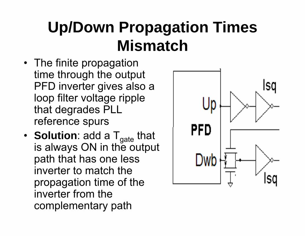
Up/Down Propagation Times Mismatch
• The finite propagation time through the output PFD inverter gives also a loop filter voltage ripple that degrades PLL reference spurs
• Solution: add a Tgate that is always ON in the output path that has one less inverter to match the propagation time of the inverter from the complementary path

Loop Filter Leakage Current• A leakage current at the loop filter high
impedance node discharges the integration capacitance– Reverse current of drain/source diffusion
diodes – Gate leakage in deep submicron CMOS
FETs• Need to compensate the leakage current by
injecting a net charge-pump current every reference clock cycle
• The current injected by the CP result in a VCO control voltage ripple which degrades PLL reference spurs

CP-PFD Transfer Function Dead-Zone• If the charge-pump has a large switching time, it
cannot react to small pulse width PFD control signals• The absence of an answer from CP (a Dead-Zone in
the PFD-CP transfer function) → the PLL loop is opened and the VCO clock edges can move unrestricted till the point where the CP will start reacting
• This phenomena results in a clock jitter windowequal to the dead-zone
• Solution: introduce every clock cycle a period of time when both Up and Down are active such that the charge-pump current legs turn-on before they start measuring the phase difference between reference and feedback clock edges

CP Charge Injection and Clock Feed-through
• Each time the up and down CP switches turn-off, their channel charge is injected into the loop filter determining a VCO control voltage ripple → degrades reference spurs
• Solution: Avoid the switch charge injection by adding dummy switches that capture the charge released by the turning-off switch and release the charge required to create the channel in the turning-on switch
• Finite Cgd capacitances of the FET switches determine the clock feed-through from the PFD control lines to the loop filter voltage, resulting in a ripple on the oscillator control signal → degrades reference spurs
• Solutions: – reduce the size of the switches → decrease Cgd– Use a smaller control voltage swing

Charge Sharing between CP nodes• Finite capacitances exist at the drains of the Up/Down CP
current mirrors• When the CP switches turn-off the Up/Down currents
discharge these nodes to the corresponding supply line (Vdd/Vss)
• When the CP switches turn-on again, these parasitic capacitances need to be charged to the loop filter control voltage (Vctrl)
• Depending on the Vctrl voltage level a net charge need to come from the loop filter capacitor to charge the parasitic capacitances → generates a Vctrl ripple which degrades PLL reference spurs
• Solution: Use a bootstrap buffer which keeps the potential at the drains of the current sources equal to Vctrl when the CP switches are OFF

Delay in the PLL Feedback Loop• All digital circuits have a finite delay time (inverter buffers,
PFD, Feedback Divider)• A delay block exp(-s*Td) introduces a linear varying phase
shift as a function of frequency φ=-ω*Td
• This phase lag degrades PLL’s phase margin by ∆φ=ωC*Td
• Feedback loop delay is particularly troublesome in large bandwidth PLLs (e.g. fast locking ring oscillator PLLs) where ∆φ=ωC*Td can assume large values
• A degraded phase margin leads to:– More peaking in the transient locking waveform which can stress
in frequency the divider if it has a small margin from its maximum operating frequency
– Peaking in the jitter input-output transfer function which degrades the output clock phase noise performance

PLL Sampling Effect• The phase comparison is not done continuously, but in a
discrete time manner → PFD compares the phases of the reference and feedback clock only based on their edge position which lead to a sampled data system
• After the phase comparison is done, no other action is took till the next reference clock cycle → this is equivalent with a hold operation applied to the phase difference measurement
• The transfer function of a zero-order hold sampled data system is (1-exp(-s*T))/s*T
• This intrinsic PLL phase sample and hold operation introduces a phase lag in the feedback loop which degrades the PLL phase margin → jitter peaking
• φ=-ω*T/2 → ∆φ=ωC*Td /2

Divider Failure During Transient Locking
• In many multi-GHz PLLs the feedback divider operates close to the maximum frequency allowed by the CMOS process, which leaves very little margin for peaking during the transient locking process
• There are two main causes for transient peaking– Poor loop damping (small signal behavior) → use a process
independent damping factor architecture which keeps ξ >1– Large phase difference between reference and feedback clock at
the point when the frequency locking is achieved and the phase locking starts → this peaking can be very large in wide-bandwidth PLLs where the oscillator control voltage can vary with a large ∆even in a single reference clock cycle
• If during the transient locking the maximum operating frequency of the divider is exceeded and it fails to provide an output edge → PLL fails to lock and fails to recover

Divider Failure During Transient Locking - Continued
• Solution 1 (for small signal peaking)– The peaking of a linear system is proportional with the input signal
step (frequency change)– To minimize the transient locking peaking at frequency change in the
synthesizer the output frequency range is divided in several sub-ranges and thus the single large step locking process is replaced with several smaller frequency steps locking processes, leading to a much lower peaking amplitude
• Solution 2 (for nonlinear peaking)– Add a circuit in the PFD that limits the maximum Up control
signals pulse width to a fraction of the reference clock period (e.g. Tref/4 or Tref/8) – undershoot during transient locking is not an issue
– Limiting the maximum pump-up time period reduces the nonlinear peaking amplitude
– Restricting the pump-up period increases the frequency locking process – can become an issue in fast frequency switching PLLs

PLL Phase Noise Analysis• Reference clock path (XTAL, REF-BUF) phase noise is
low-pass filtered by the PLL → low phase noise output clock asks for a low loop bandwidth
• Charge-pump noise is also low-pass filtered as all the front-end noise components
• Controlled oscillator phase noise is high-pass filtered by the PLL → high phase noise oscillators (ring oscillators) require a low loop bandwidth
• Loop filter noise is band-pass filtered by the PLL• All corner frequencies of the low-pass/high-pass/band-pass
transfer functions are equal to the loop natural frequency• LC oscillator based PLLs use low loop bandwidths → does
not have demanding requirements for reference path noise• Ring oscillator based PLLs use high loop bandwidths to
adequately reject VCO’s large phase noise → need a low phase noise reference path

Example of PLL Output Phase Noise

PLL Output Clock Spurs• DIRECT INJECTION SPURS• Reference spurs → generated by a finite ripple on the
oscillator control signal at the reference clock frequency →fspur = fout ± fref
• Supply injected spurs → determined by a finite PSRR of the PLL blocks → fspur = fout ± fperturb
• MIXING SPURS• Nonlinear operations such as clock edge squaring and
charge-pump chopping action are capable of creating intermodulation frequencies fspur = k*fref ± p*fperturb
• If the intermodulation spurs fall in the PLL bandwidth where minimal rejection exists → large output spurs can be generated → need high PSRR regulators
• The spurs in the REF-BUF are amplified by the PLL gain (N)

Crystal Oscillators Requirements• Keep the amplitude constant with process and temperature → need to use an Automatic Amplitude Control loop (AAC)
• Maximizing the oscillating amplitude (without crashing the active devices) → minimizes the oscillator phase noise
• Reducing thermal noise in amplifier and AAC loop decreases the 1/f2 phase noise while reducing 1/f noise in amplifier and AAC loop decreases the 1/f3 phase noise
• Minimize the resistive and capacitive loading on the crystal → keeps a high loaded Q of the tank → improves 1/f2 phase noise performance
• Ensure a safe oscillator start-up requires a positive loop gain higher than 1 over all design corners. Optimum value from phase noise perspective is 2 → keep the loop gain 1.5-3 over process and temperature corners

XTAL Oscillators Configurations• Common-source amplifier (Pierce Oscillator)
↑ does not need floating capacitors → all capacitors can be MOS↓ need two pins to connect the crystal↓ use both NFETs and PFETs → increased 1/f3 phase noise↓ bias network loads the crystal → degraded loaded Q↓ need a linear buffer if the sinusoidal clock need to be driven off-chip
• Common-drain Amplifier (Colpitts Oscillator)↑ need a single pin to connect the crystal↑ does not need a linear clock buffer to drive the sine-clock off-chip↑ can use only PFETs → minimize 1/f3 phase noise↑ show lower loading on the crystal tank → higher Q → minimize 1/f2
phase noise↓ need a floating capacitor (MIM or Metal Cap. which takes21 a large
die area) → cannot be implemented with MOS capacitors due to their large substrate noise injection

XTAL Oscillators Configurations -Continued
• Common-gate amplifier (also Colpitts Oscillator)↑ need a single pin to connect the crystal↑ can use only PFETs → minimize 1/f3 phase noise↓ need a floating capacitor (MIM or Metal Cap. → large die
area)↓ difficulties to bias the amplifier as both the drain and
source need to see large impedances → headroom voltage issue
• Pierce oscillator → widely used for their area efficiency
• Colpitts oscillators → preferred in low phase noise applications → require larger die area
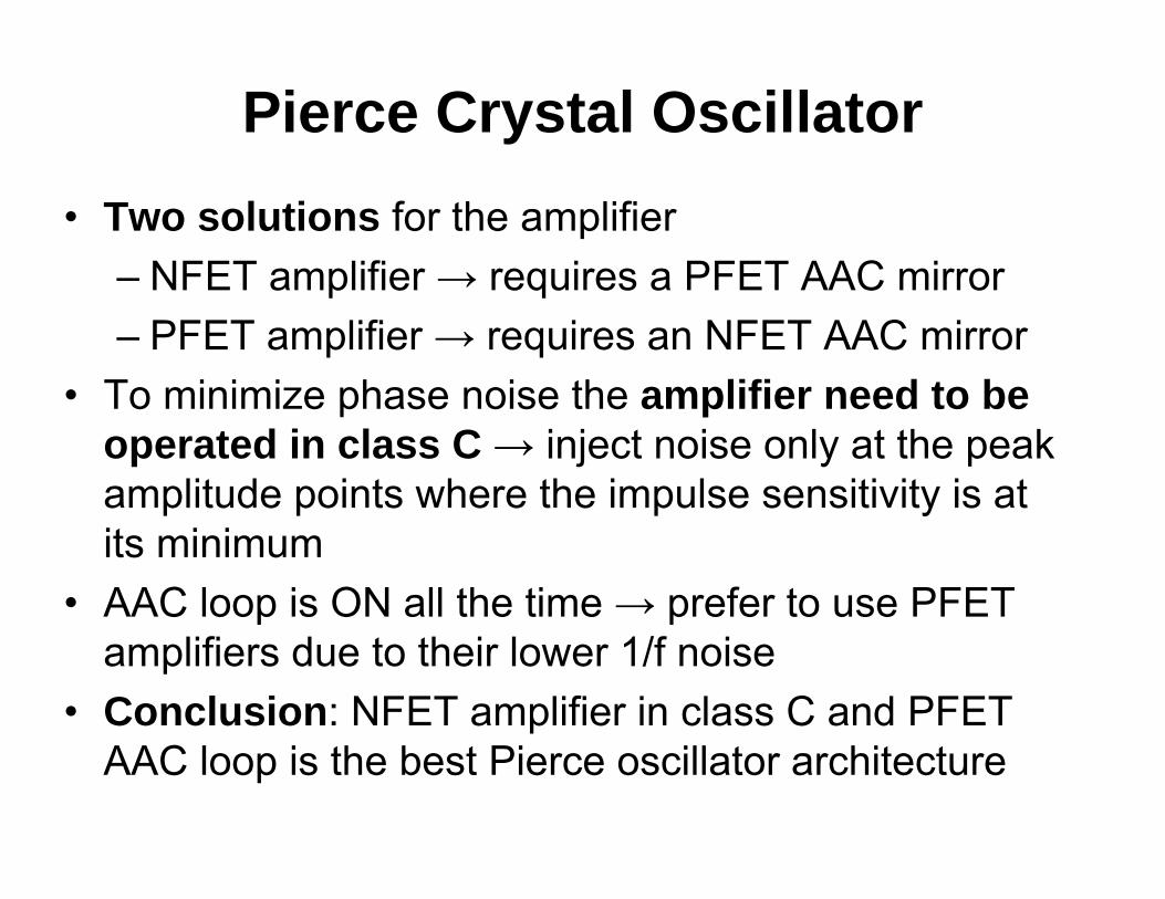
Pierce Crystal Oscillator• Two solutions for the amplifier
– NFET amplifier → requires a PFET AAC mirror– PFET amplifier → requires an NFET AAC mirror
• To minimize phase noise the amplifier need to be operated in class C → inject noise only at the peak amplitude points where the impulse sensitivity is at its minimum
• AAC loop is ON all the time → prefer to use PFET amplifiers due to their lower 1/f noise
• Conclusion: NFET amplifier in class C and PFET AAC loop is the best Pierce oscillator architecture

NFET Amplifier Pierce Oscillator• Use thin oxide devices to
reduce the 1/f3 phase noise (thick oxide devices have larger 1/f noise at same device area)
• Amplitude decreases (lower breakdown voltage) →decrease S/N
• Rbias ensures a diode DC connection → need to be large to avoid loading the crystal
• Rshift shifts-up the DC voltage in the drain of the amplifier →achieves a larger amplitude →lower phase noise
• Avoid crushing the amplifier →reduce the 1/f2 phase noise

PFET Common-drain Oscillator• Use PFET amplifier and PFET
AAC to minimize 1/f3 p. noise• Using a current load in the
source of the amplifier prevents the class C operation → need to use a current mirror architecture
• M20,M21 mirror provides the DC bias current
• Class C operation of the amplifier → inject noise only at minimum impulse sensitivity
• Need a floating capacitor C1 that takes large area (MIM)

Automatic Amplitude Control Loop• The AAC noise generally dominates the phase noise of a
well designed XTAL oscillator → it is always ON and injects noise also around clock edges
• Without AAC the amplitude of oscillation can vary over a wide range (e.g. 2x) with process and temperature → degrade significantly the phase noise in the worst case corner
• Three available types of AAC:– Continuous time AAC → adjust continuously the bias
current of the amplifier based on the measured peak amplitude → add noise during the entire clock cycle
– Hybrid continuous-discrete AAC → perform the amplitude correction only at discrete time intervals but still use an AAC loop amplifier
– Discrete AAC → replace AAC amplifier with a digital state machine that takes the decision for the loop drive direction

Continuous Time AAC Loops• Use positive and negative peak
detectors to measure the peak-to-peak amplitude
• Prefer AC coupling of peak detectors→separate bias points
• OTA sets the bias current of the amplifier such that the measured amplitude equals the reference voltage (VTp+VTn)
• PFET OTA and PFET bias mirror → minimize 1/f3 p. noise
• Use large resistive degeneration to reduce the thermal noise of the bias mirror
• PN ≈ -125dBc/Hz @1KHz

Discrete Time AAC Loops• AAC amplifier is the dominant
noise contributor → replace it with a digital state machinewhich takes the decision for driving the AAC loop
• Need an ADC to convert the measured peak amplitude into a digital control word for the state machine
• Need a DAC to convert back to current (analog) the state machine output
• Both ADC and DAC need only moderate resolutions (6-8 bit)
• PN ≈ -145dBc/Hz @1KHz

Reference Clock Squaring Buffer• Square-up the sinusoidal clock from the crystal
oscillator with minimal added noise• Present a rather constant input impedance to the
crystal oscillator → do not impact its phase noise• First buffer stage generally dominates the noise of
the squaring buffer → need high gain to speed-up the clock edges → second stage need to present a low capacitive load to the first stage
• Spurs present on the supply line are down-converted around the reference clock carrier →need a high PSRR regulator
• Noise on the supply line is up and down-converted around the carrier → need a low noise regulator

Reference Clock Squaring Buffer
• AC coupled to avoid pulse width distortion due to XTAL bias point variation with process and temperature
• First inverter need to have a high gain, low thermal noiseand low 1/f noise → large device area and high W/L
• The second buffer need to be small to minimize load on the first stage → only large enough to just pass the fast edges created by the first stage
• Scale-up following buffers to ensure PFD driving requirements• The number of inverters need to be selected such that PFD is
driven by the XTAL edge that has lower phase noise

Current Starved Squaring Buffer• Limit the current available to the
inverter around the crossover point →minimize phase noise as only one of the two devices in the inverter is ON at a given time (use a VTp+VTn supply)
• Rbias resistor that provides the DC bias to the first inverter shows a negligible load to the crystal oscillator
• slows-down slightly the edges but the gain from the reduced noise is larger
• Use an open loop shunt regulator to avoid reference spurs leakage to the global PLL supply– Low freq. PSRR limited by rout(Ibias)/(2/gm)– High freq. PSRR limited by Cgd(Ibias)/Cf

Phase Frequency Detector Requirements
• Fast reset propagation time to minimize the width of the up/down pulses in lock condition → improve reference spurs due to less CP mismatch current injected in the loop filter
• Fast rise/fall times to reduce the sensitivity to both gate intrinsic noise and supply noise → minimize PFD phase noise contribution
• Matched propagation times for up/upb/dw/dwbcontrol signals → improve reference spurs
• Matched slew-rates for the four PFD output signals up/upb/dw/dwb
• Provide the voltage level shifting required by the CP

7 NAND Gate PFD
• The faster input of the NAND gate (the NFET closer to the output) need to be used for the reset propagation signal
• The up/dw pulse width in lock condition is equal with 7*Tdelayof the NAND gate and is limited to 0.35-1ns → reference spurs <50dBc
• If the CP has a slow switching time, additional inverters can beadded in the reset path such that the minimum up/dw pulse width is extended in excess of the Tcp switching time → no dead zone in the CP-PFD transfer function

Dynamic D-Flip-Flop PFD• To reduce the reset
propagation time (which limits the up/dw pulse witdh) the PFD can be implemented with dynamic (pre-charged) DFFs
• The NMOS NAND gate used for the reset decoding is much faster that the standard CMOS gate, reducing the up/down pulse width → DC current
• DFF sensitive to the XTAL falling edge witch has less phase noise (PFET is driving)

Dynamic DFF PFD with EmbededReset NAND Gate
• To further reduce the reset propagation time the reset NAND gate was built-in the dynamic DFF
• The up/dw pulse width is reduced to 3*Tdelay=150ps →reference spurs decrease to -60…65dBc
• DFF sensitive to rising edge →need an additional inverter at each input in order to still use the lower phase noise edge

Balancing the Propagation Times and Slew-Rates of PFD Output
• The PFD provides only two outputs (up/dw), while the differential current steering CP requires also the upb/dwb complementary signals
• Upb/dwb obtained by adding a parallel path having one extra inverter
• Add always-ON transmission gatesTu/Td to balance the extra inverter delay
• After t-gates the edges are slower in comparison with the inverter output
• Add two more layers of inverters to balance the slew rates of all 4 PFD outputs

PFD Level Shifters• For fast propagation times the PFD need to use the
thin oxide devices from a dual gate oxide CMOS process (e.g. 0.13µm from a 0.13µm CMOS) and a low supply voltage (1.3V)
• In contrast the charge-pump need to use thick oxide devices and higher supply voltage (0.35 µm from a 0.13µm CMOS and 2.5-3.3V)
• A level shifter need to be introduced between the PFD and the CP to make the conversion between the two logic signals– Need to maintain fast edges– Minimize power consumption
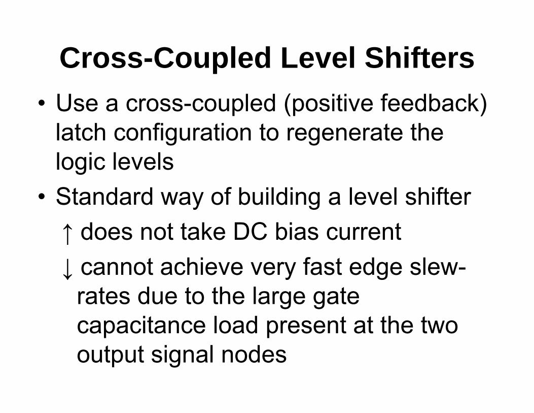
Cross-Coupled Level Shifters• Use a cross-coupled (positive feedback)
latch configuration to regenerate the logic levels
• Standard way of building a level shifter↑ does not take DC bias current↓ cannot achieve very fast edge slew-
rates due to the large gate capacitance load present at the two output signal nodes

Mirror-Protected Level Shifter↑ does not use cross-coupled
structures that load excessively the signal nodes → much faster edge speed
↓ need a DC bias current- pulling-down is provided by the Mdw low voltage FET- pulling-up is ensured by the Mup high voltage FET - Mprot high voltage current mirror protects the Mdw FET when the output is High

Charge-Pump Requirements• Equal Iup and Idown for all output voltage
levels → reduce reference spurs• High output impedance → reduce current
mismatch and also improves PSRR• Equal up/down switching times (combined
with PFD outputs propagation times)• Low thermal and 1/f noise → large area and
low gm devices → need large headroom• Low clock feed-through → dummy switches• Low supply and substrate coupled spurs

Charge-Pump Architectures• Single ended CP
↑ lower loop filter capacitance↓ higher substrate/supply noise coupling
• Differential-In Single-ended-out CP↑ still does not need double loop filter capacitance↑ Faster switching (current steering)↑ less spur sensitivity
• Differential-In Differential-Out CP↑ best supply/substrate/clock feed-through performance↓ need double loop filter capacitance area↓ Need a common-mode feedback circuit that increases CP
noise contribution
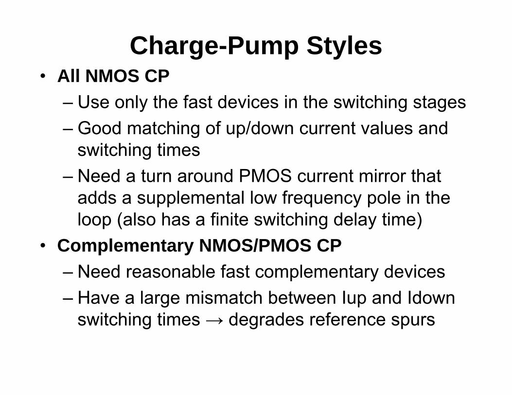
Charge-Pump Styles• All NMOS CP
– Use only the fast devices in the switching stages– Good matching of up/down current values and
switching times– Need a turn around PMOS current mirror that
adds a supplemental low frequency pole in the loop (also has a finite switching delay time)
• Complementary NMOS/PMOS CP– Need reasonable fast complementary devices– Have a large mismatch between Iup and Idown
switching times → degrades reference spurs

Charge-Pump Configurations• Drain-switch
– Large current spikes at beginning of the turn-on when both the current mirror and the cascode switch are in triode region
– Large clock feed-through (switch connected directly to the loop filter)
– Relatively long switching time• Source-switch (best single ended CP)
– Fast switching (switch connected at a low impedance node)
– Less clock feed-through (switch is not directly connected to the loop filter)
– Low switching spikes (devices switch between OFF and On in saturation region)
• Gate-switch → slow – not used in single ended form
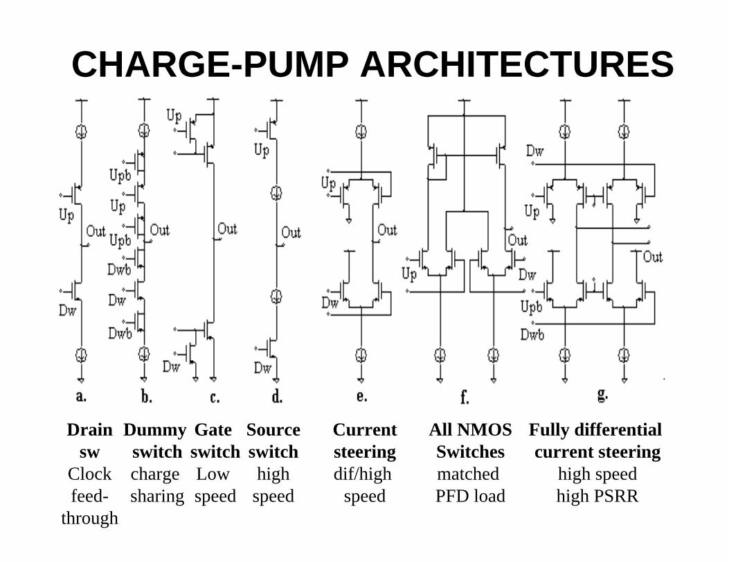
CHARGE-PUMP ARCHITECTURES
Drain sw
Clock feed-
through
Dummy switchcharge sharing
Gate switchLow speed
Sourceswitchhighspeed
Currentsteeringdif/high
speed
All NMOSSwitchesmatched PFD load
Fully differential current steering
high speedhigh PSRR

CP Charge-Injection Compensation- Use half size devices to
compensate the channel charge-injection → works well for very fast switching when charge splits half/half between source and drain
- For a good cancellation a good matching between up/upb/dw/dwb is required →otherwise charge is cancelled in average over one period, but VCO control voltage has ripple →increase reference spurs

CP with Charge Sharing Cancellation• OAbuf keep the dummy output
at the same potential as the loop filter → avoid charge sharing from dummy side
• Use equal size dummy switches such that simultaneous charge-injection and clock feed-through is realized → Each output node sees two Cgd capacitors connected at opposite sign signals
• Not perfect cancellation of charge injection → main switches are in saturation while the dummy switches are in triode

Dynamic biasing Charge-Pump• To ensure a perfect match of
up and down currents for a wide range of output voltages → use a DC feedback loop to control the PFET current mirror
• Reference voltage is took from the dummy leg which is kept by OAbuf at the loop filter voltage
• OAmatch drives the PFET mirror such that to up and down currents are equal for all Vctrl values
• Sense node is given by a replica current leg that is always ON

Reduced Swing Differential-in CP• The clock feed-through
depends on Cgd value and on the swing of the digital control signals
• Use a reduced swing control voltage to drive the current steering switches (between the cascode voltage and the corresponding supply line)
• The switches are operated between OFF and ON in saturation region → they act also as cascode devices, increasing the output impedance

Single-Sided Switching Current Steering Charge-Pump
• The devices connected to the loop filter have their gates always connected to the constant cascode voltages →minimize clock feed-through
• The switching devices are connected to the dummy side of the CP
• Single sided switching works fine for medium output control voltage range, but has leakage issues for wide ranges

Charge-Pump Noise Contribution• The CP input bias current noise
is first order rejected as it is mirrored both to the up and down currents
• The up/down current mirrors have noise contributed both by their input master devicesand output slave devices
• To cut the CP noise in half a low corner frequency RC filterwas interposed between the master and the slave devices of the current mirrors
• Integrated noise of the master devices is reduced to KT/C

Spur Down-Conversion Mechanism• The switching action of the charge-pump is
capable of down-converting high frequency spurs/noise present on the supply lines (e.g. coming from another PLL or other switching circuits of the ASIC)
• If the down-converted spur falls into the bandwidth of the PLL → minimal rejection is present and the spur appears at the output low-pass filtered with fn corner frequency
• Minimizing the spur down-conversion →requires filtering of the CP supply line

CP Supply Filtering Techniques• Passive RC filter
– The R is limited by the headroom voltage loss
– C is limited by die area– Pole position in MHz range
• Active RC filter– Need a zero-VT FET follower to
provide the load current with a minimal VGS voltage drop
– R limited by the output voltage noise
– Pole position in KHz range

Loop Filter Requirements• Low noise contribution → few active devices or
passive• Low reference spurs → minimize CP up/down
pulses or isolate oscillator control input from CP switching
• Low supply injected spurs → no supply connection (passive) or use a regulator
• Low area → limit the total capacitors size →compromise with noise
• Provide gain → Active loop filter → reduce C size• Tunable time constants → switches add clock feed-
through and current leakage → limit reference spurs

Continuous-Time RC Loop Filter• Simplicity → passive
configuration• Low noise contribution - no
active devices• Very high PSRR → no
supply connection• All capacitors are connected
to GND → can be implemented with MOSFETs
• Need large capacitors in low noise applications (small R to reduce noise → large C)
• Does not isolate oscillator from CP switching

Switched Capacitor Resistor RC Filter• To reduce the noise the
stabilizing zero resistor was simulated with a switched capacitor network
• Noise is limited by KT/C →can be made small using large C
• Need 4 additional switches that may degrade reference spurs due to their clock feed-through and channel charge injection
• Keep all the other drawbacks of the standard RC loop filter
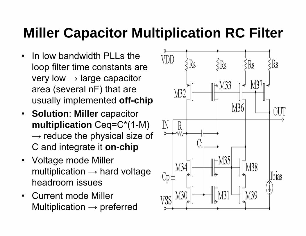
Miller Capacitor Multiplication RC Filter• In low bandwidth PLLs the
loop filter time constants are very low → large capacitor area (several nF) that are usually implemented off-chip
• Solution: Miller capacitor multiplication Ceq=C*(1-M) → reduce the physical size of C and integrate it on-chip
• Voltage mode Miller multiplication → hard voltage headroom issues
• Current mode Miller Multiplication → preferred

Noiseless Resistor Multiplication Filter• Instead of multiplying C we can
multiply R to reduce the capacitor size
• Want Req=R*M, but without getting the corresponding noise (noiseless multiplication)
• Use a second charge-pump that injects a current M times larger than the main charge-pump directly into the resistor
• R appears multiplied for the zero position, but not for the pole position → need to increase Cp by the same M factor (Cp << Ci)
• Still a passive filter → low noise contribution
• Require a floating capacitor →large area (MIM or Metal capacitor)

2 OpAmp V-Mode Feed-Forward Filter• Alternative way to create the
stabilizing zero → feed-forward path
• VCOs need a voltage-mode filter (can use or not Miller capacitance multiplication)
• Ci is reduced by the ratio of the two charge-pump currents
• Need two operational amplifiers → more noise and larger power dissipation
• Use active devices → PSRR is a concern

1 OpAmp V-Mode Feed-Forward Filter
• To minimize the noise introduced by the loop filter a single OpAmparchitecture was developed
• The OAbuf isolates the Ci capacitor from the proportional path (leakage current)
• The summation is done by connecting in seriesthe integral and proportional voltages

Current-Mode Feed-Forward Filter• Appropriate for ICO PLLs• The integral and proportional
control currents are summed directly at the output node without the need of a summing amplifier
• The integral and proportional transconductance stages can be made low noise by using large source resistor degeneration
• For VCO based PLLs an output resistor is used to convert back to voltage (large current for low noise)

Reduce the PLL Reference Spurs• Solution 1: reduce the up/down pulse width
(require a fast switching CP and fast reset PFD) → spurs as low as -60dBc
• Solution 2: isolate the oscillator from the charge-pump switching and distribute the proportional control energy over an entire reference clock period → use a sample and hold proportional path (ref. spurs –70..80dBc) – Measure the phase difference– Apply a constant proportional control signal– Reset the proportional path each reference cycle

Hybrid Continuous-sampled loop filter• Only the proportional path is
implemented with a sampled structure (higher charge-pump current)
• Need to separate the phase sampling and reset operations from the phase holding →provide a continuous control signal to the oscillator → dual proportional path operated in tandem → 2 CPs
• The ripple pole is still implemented with a continuous time RC filter → add some extra noise

Fully sampled loop filter• For best reference spurs
rejection both integral and proportional paths need to use sampled configurations
• If a higher crystal oscillator frequency is available than a different architecture can be used to provide a continuous oscillator control signal – isolation windowing
• The oscillator is isolated only for a ±∆Tref/M time period around the reference clock active edge (small phase offset when in lock)
• Digital pole → lower noise

LC Oscillator Requirements• Integrated oscillators need a differential amplifier →
reduce the supply and substrate noise sensitivity• High frequency operation → minimize parasitic
capacitances• Low oscillator gain → reduces both output clock
phase noise and spurs → requires a wide range control signal
• Good symmetry of the waveform → lowers 1/f noise up-conversion
• Reduce the noise coming from the tail bias current• Minimize supply voltage dependent capacitors
connected to the tank → minimize supply pushing
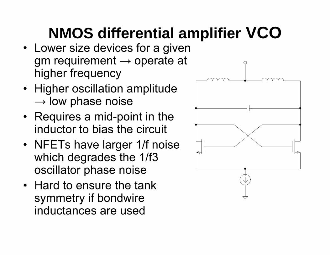
NMOS differential amplifier VCO• Lower size devices for a given
gm requirement → operate at higher frequency
• Higher oscillation amplitude → low phase noise
• Requires a mid-point in the inductor to bias the circuit
• NFETs have larger 1/f noise which degrades the 1/f3 oscillator phase noise
• Hard to ensure the tank symmetry if bondwireinductances are used

PMOS differential amplifier VCO• PFETs have much lower 1/f
noise (due to their buried channel) → achieve a much lower 1/f3 phase noise
• Need a higher current in comparison with the NFET VCO
• Need larger size devices →lowers the maximum operating frequency
• Need a mid-point in the inductor for bias purposes-not suitable for bondwireinductances

CMOS differential amplifier VCO• Requires a lower supply
current due to the stacked gm configuration
• Can use bondwireinductances as no mid-point is required
• Provide a more symmetric waveform → lower 1/f noise up-conversion
• Lower Oscillator amplitude →degrades slightly the phase noise performance

Voltage-mode versus Current-modeLC VCOs
• Current-mode– The amplitude is determined
by the tail current value– Tail current 1/f noise is up-
converted around the carrier– Does not require a precise
value supply voltage• Voltage-mode
– Amplitude determined by the supply voltage value →requires a calibrated regulator
– Does not have a tail current source → lower 1/f3 phase noise

Reduce the tail current Source Noise• Resistor degeneration
– Reduce both the 1/f and thermal noise coming from the tail source
– Takes away headroom → lowers the oscillating amplitude
• LC filter at 2*fo– Filter the second order harmonic seen
by the tail current mirror– Effective at 1-5GHz– @ high frequency hard to achieve large
value inductors with self-resonating frequency > 10-20GHz
• Tail resistor instead of current– No 1/f noise and lower thermal noise– Calibrated resistor to set amplitude

Bondwire versus Planar Inductors• Bondwire inductors:
– No additional process steps– Highest Q available = 40-50– High self-resonating frequency >20GHz– Limited value (0.2-0.3nH if bonding between two pads, 1-
3nH if bonding from the die to the package and then back to the die
– Poor symmetry if a mid-point is required for bias• Planar inductors:
– Can provide a well controlled mid-point for bias purposes– Lower Q=10-20 due mainly to substrate losses– Lower self resonating frequency due to parasitic cap.– Need supplementary processing steps to be added to
standard CMOS (use thick metal layers)

Supply Voltage Requirements• Spurs in the LC oscillator supply
line are up-converted around the carrier → need a high PSRR reg.
• Noise on the supply lines is up-converted into phase noise skirts → need a low noise regulator
• To minimize second order harmonics on oscillator supply →use a series LC circuit which resonates at 2*fo
• Using a MIM capacitor and a bondwire inductance provides a sharp attenuation

Automatic Amplitude Control Loop• Maintain the maximum oscillating
amplitude allowed by the available supply voltage →optimize phase noise
• AAC loop degrades phase noise• Use a high frequency peak
detector to measure amplitude• Use an amplifier to compare the
amplitude against a reference voltage (need to be low noise)
• Adjust the element that sets the amplitude (current, resistor or voltage)
Reduce the Phase-Noise of the AAC• Continuous time AAC loop:
– Use PFET stages in both the AAC amplifier and the peak detectors (less 1/f noise)
• Hybrid continuous-discrete AAC loop:– Close the loop only at discrete times (e.g. at
power-up to compensate the process variation, and in the blind spots of the communication link to compensate both process and temperature variations)
• Discrete time AAC loop:– Eliminate the noise of the amplifier by replacing it
with a digital state machine

Reduce the Oscillator Gain• Achieving a large tuning range while having a
low oscillator gain requires frequency calibration → not for fast frequency changing PLLs (e.g. frequency hoping synthesizers)
• First the frequency is calibrated in open-loopusing a capacitor DAC connected in parallel with the LC tank → bring the frequency to within few % of the target value
• The final frequency tuning is realized in closed-loop using a PLL loop that controls a low tuning gain varactor

Calibration Capacitor DAC• Use a differential capacitor →
better tank symmetry• Floating switch → 1 FET →
lower Ron and less parasitic capacitors
• Reduce Ron by pulling to GND the drain/source of the OFF switch
• Reduce Cjd/Cjs by pulling to Vreg the drain/source of the ON switch
• Rb keep floating the capacitor that is switched-off the LC tank
• Rc reduces the impact of the Cgs and Cgd capacitances
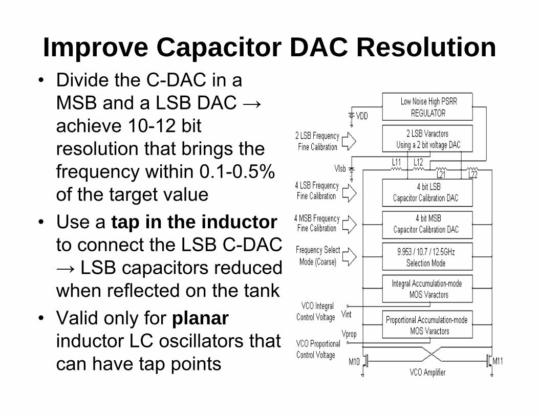
Improve Capacitor DAC Resolution• Divide the C-DAC in a
MSB and a LSB DAC →achieve 10-12 bit resolution that brings the frequency within 0.1-0.5% of the target value
• Use a tap in the inductorto connect the LSB C-DAC → LSB capacitors reduced when reflected on the tank
• Valid only for planar inductor LC oscillators that can have tap points

Improve Capacitor DAC Resolution• Use a tap in a capacitor
divider to connect the LSB C-DAC → suited for bondwire inductance LC oscillators that do not have taps in the inductor
• The LSB capacitors appear reduced when reflected on the LC tank
• Need to provide DC bias to the floating nodes between capacitors → avoid device breakdown
Varactor Used in LC oscillators
• Reverse biased diode varactors– Relatively poor quality factor at multi-GHz
frequencies (Q=5-10) due to the series resistance of the non-depleted silicon layer R(freq)
– Highly non-linear C(V) characteristic• Accumulation MOS capacitors
– Higher quality factor at high frequencies Q=10-20– Larger process and temperature variation →
need a wider range open-loop calibration– Highly non-linear C(V) characteristic

Constant Gain Varactor• Use several accumulation MOS
capacitors connected in parallel which have their DC bias shifted such that their peak gain points are uniformly distributed over the entire control voltage range
• Gain ripple depends on the number of cells connected in parallel
• The different DC offset voltages for the parallel varactor legs can be generated with a simple resistor divider biased from a low noise voltage
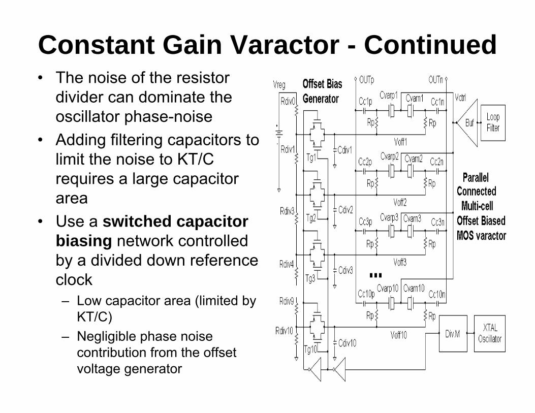
Constant Gain Varactor - Continued• The noise of the resistor
divider can dominate the oscillator phase-noise
• Adding filtering capacitors to limit the noise to KT/C requires a large capacitor area
• Use a switched capacitor biasing network controlled by a divided down reference clock– Low capacitor area (limited by
KT/C)– Negligible phase noise
contribution from the offset voltage generator

Ring Oscillator Requirements• Operate at GHz frequencies → minimize the
number of stages in the ring (4 – provide quadrature outputs, 3 – safe operation, 2-highest frequency, but need extra phase shift)
• Have a wide tuning range (several GHz) →result in a very large VCO gain, which increases the sensitivity to PLL front-end noise and spurs
• Minimize noise coming from biasing circuitry• Need a high PSRR, low noise regulator to
avoid supply noise and spurs injection

Single-Ended versus Differential• Single-ended inverters offer a
lower intrinsic noise due to a lower device count and also a lower power consumption– Better in SOI processes that
have negligible substrate capacitances
• In large mixed analog-digital ICs the supply and substrate noise and spur injection dominate
• Differential inverters offer better supply and substrate rejection

Single-Ended versus Differential
• Differential inverters give a more symmetric waveform → reduces 1/f noise up-conversion
• Less supply and substrate injection particularly in balanced load differential stages
• They have a larger active device count → more intrinsic noise
• Need larger supply current for a given operating frequency
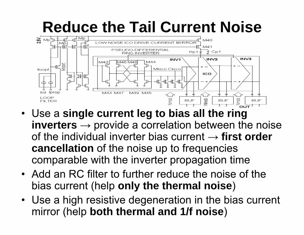
Reduce the Tail Current Noise
• Use a single current leg to bias all the ring inverters → provide a correlation between the noise of the individual inverter bias current → first order cancellation of the noise up to frequencies comparable with the inverter propagation time
• Add an RC filter to further reduce the noise of the bias current (help only the thermal noise)
• Use a high resistive degeneration in the bias current mirror (help both thermal and 1/f noise)

Saturated Load Differential Inverter• Saturated load → larger
amplitude of oscillation →reduces intrinsic phase noise
• Higher supply noise and spur injection → in the unbalancedcondition when one of the load devices is in triode and the other one is OFF
• NFET inverter– Lower current → higher
frequency– Larger 1/f noise
• PFET inverter– Lower 1/f noise– Higher bias current for given
frequency
→

Clamped Amplitude Saturated Load• To avoid strong supply
noise and spurs injection the output amplitude can be clamped both in the positive and negative direction → avoid going in triode of both amplifier and load devices
• Reduces slightly the amplitude → limited intrinsic phase noise degradation

Triode Mode Differential Inverter• Voltage controlled resistor
load implemented with MOSFETs in triode region
• Balanced load → improve the supply rejection
• Smaller amplitude → allows higher oscillating frequency
• Replica bias leg generate a tail current that keeps the amplitude constant
• Triode load FTEs do not have 1/f noise while PFET amplifier has low 1/f noise

Reduced 1/f Noise Up-Conversion• To reduce 1/f noise up-
conversion the waveform need to be as symmetric as possible
• Use a weak positive feedback NFET and PFET latch to balance the waveform rise/fall times
• However the supplementary gate capacitance load from the latch stage reduces the maximum oscillating frequency

Pseudo-Differential Inverter Ring• Two single-ended inverter rings are coupled with weak
gain inverter latches → ensure a tight synchronism between the positive and negative clock paths
• High symmetry of the waveform → reduce the 1/f noise up-conversion
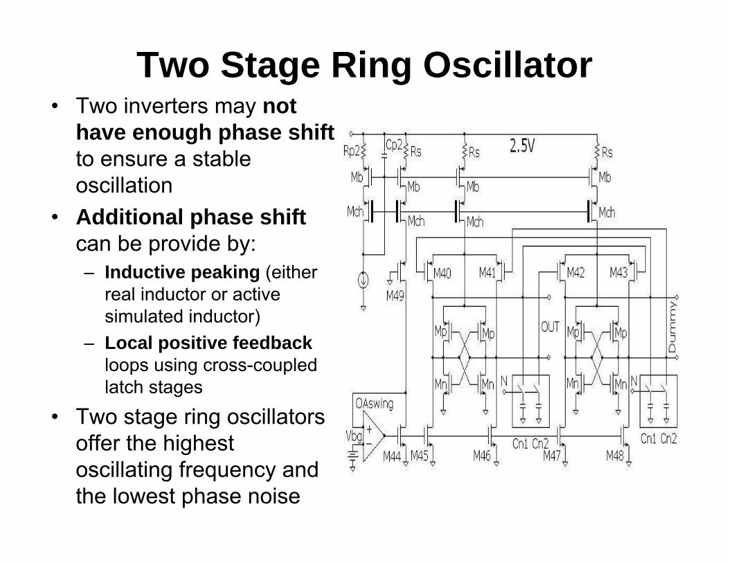
Two Stage Ring Oscillator• Two inverters may not
have enough phase shiftto ensure a stable oscillation
• Additional phase shiftcan be provide by:– Inductive peaking (either
real inductor or active simulated inductor)
– Local positive feedbackloops using cross-coupled latch stages
• Two stage ring oscillators offer the highest oscillating frequency and the lowest phase noise

VCO Clock-Buffer Requirements• Most applications require a 50% duty cycle• Present a low capacitive load to the oscillator (prefer a
constant capacitance rather than C(V))• Ensure a symmetric loading to all the ring inverters • Square-up the sine/triangular waveform provided by the
VCO (hard to get large gains at multi-GHz frequencies)• Avoid coupling supply noise and spurs → VCO-BUF uses
the same regulated supply as the VCO - the impulsive supply current of the buffer does not impact VCO phase noise as it is in perfect synchronism with the generated clock
• Second order distortions resulted from the asymmetry (e.g. VT mismatch) can degrade oscillator’s phase noise
→

50% Duty Cycle Clock• At lower frequencies the established way of
ensuring a 50% duty cycle is to run the oscillator at twice the required output frequency and than divide by 2↓ power hungry solution → the VCO runs at twice
the frequency↓ not applicable to 5-10GHz PLLs due to the limited
gain-bandwidth of the CMOS inverters• Dividing down the VCO output clock also
ensures quadrature outputs - required by most communication systems

Dual Shunt-Feedback 50% Duty Cycle VCO-Buffer
• Use a differential pair with dual shunt feedback:– Resistor feedback →
restricts the output swing around the trip point of the 2nd inverter
– Inverter feedback →matches the trip point of the first two stages in the VCO-BUF, ensuring a precise 50% duty cycle over process and temp.

Mixed NMOS-CMOS 50% Duty Cycle VCO-Buffer
• CMOS inverters have a large input capacitance → prefer NMOS inverters which are faster and present a lower input capacitance (but have less drive capability)
• The front-end is built with pseudo-differential NMOS stages → ensure fast edges
• Back-end is CMOS → large drive capability• Cascaded resistive shunt feedback stages ensure the 50%
duty cycle

Pseudo-Differential Buffer
• The highest bandwidth in a given process is achieved by single ended inverter stages
• Use two single ended signal paths to achieve a pseudo-differential clock path
• AC coupling is used to avoid pulse width distortion• Use Cc after each 2 inverters to avoid large offset voltage
acummulation• First two stages of equal size to square-up the waveform
and than scale-up the size for drive capability
High-frequency Divider Requirements• Ensure multi-GHz operation• Avoid large supply currents (need a high
reverse PSRR shunt regulator to isolate the impulsive supply current from the global PLL supply)
• Digital design styles:– Standard CMOS → usually not enough fast– CML CMOS logic → fastest, but need large
DC current– Dynamic CMOS logic → fast operation and
no DC current

Divider Phase Noise / Jitter• The different clock paths within the divider
can add significant amount of phase noise/jitter
• To minimize divider jitter the output divided-down clock is re-synchronized either at the full VCO rate (if possible) or at a lower rate (f0/2, fo/4)
• By re-synchronizing all jitter introduced by the divider is eliminated → jitter limited by the last re-synchronization DFF and its clock buffer
→

Dual Modulus Divider Architecture
• The pre-scalar has a controlled division modulus (2/3, 4/5, 8/9, etc.)
• The higher the front-end division factor → lower the frequency requirements for the back-end dividers
• Back-end modulus control divider determines the N/N+1 division of the front-end
• Back-end terminal count divider generates the output clock and resets the entire divider

CONCLUSIONS• Selecting the architecture for the PLL building blocks is key
for achieving high performance multi-GHz frequency synthesizers
• XTAL oscillators → move from the widely used Pierce configuration to the lower phase noise all PFET common drain Colpitts architecture
• REF-BUF dominates the phase noise in wideband PLLs →current starved inverters offer a significantly lower noise and supply spurs sensitivity
• PFD need to have a fast reset propagation time and also fast rise/fall times → migrate from standard CMOS 7 NAND architecture to dynamic D-flip-flop configurations
• Charge-pumps need to have a fast switching and accurately matched currents and switching times → current steering is the architecture of choice with dynamic matching DC loop and charge sharing and clock-feedthrough cancellation

CONCLUSIONS - Continued• Loop filters need to add negligible noise and have a very
high PSRR. Reference spurs are a big concern in many communication applications → migrate from continuous time filters to hybrid and fully sampled filters that completely isolate the oscillator from the charge-pump switching action and spread the impulsive control energy over an entire reference clock cycle. Digital filtering further reduces the loop filter noise contribution
• LC Oscillators → migrate from current-mode towards voltage-mode architectures that provide a significantly lower 1/f noise up-conversion. Use bondwires for the tuned tank and a high resolution calibration network to reduce the oscillator gain → help both spurs and phase noise
• Ring Oscillators → Differential inverters are preferred in large mixed signal ICs due to their higher supply and substrate noise immunity. Minimize the number of inverters in the ring brings both a high frequency capability and a lower phase noise. Ensure a symmetric waveform for lower 1/f noise up-conversion and minimize the tail current noise

CONCLUSIONS - Continued• Multi-GHz clock buffers → use the simplest gain
stages available for maximum gain-bandwidth. Pseudo-differential inverter chains with AC coupling for pulse-width distortion cancellation became a standard procedure
• Multi-GHz dividers → dual modulus architectures became standard, having a high frequency front-end prescalar built with CML or dynamic CMOS logic and a low frequency back-end built with standard CMOS or dynamic logic
• Power supply partitioning and regulation is an important part of the synthesizer design → to ensure low supply injected spurs use several series and shunt regulators together with passive and active RC filtering