Embed Size (px)
Citation preview

Electrical and Electronics Engineering: An International Journal (ELELIJ) Vol 3, No 3, August 2014
DOI : 10.14810/elelij.2014.3303 31
DESIGN AND IMPLEMENTATION OF PLL
FREQUENCY SYNTHESIZER USING PE3336
IC FOR IRS APPLICATIONS
Vabya Kumar Pandit
1, Deepak V.Ingale
2, Sourabh Basu
3
1Department of RF communication Engineering, Jain University, Bangalore, India
2Jain University, Bangalore, India
3,4ISRO Satellite Centre, Bangalore, India
ABSTRACT
The design and experimental verification of a low phase noise phase locked loop (PLL) frequency
synthesizer using Peregrine’s PE83336 IC is presented. This PLL is used as frequency synthesizer which
generates stable and low phase noise signal for space applications. A stable reference frequency of
22.8MHz is provided to the PLL through a temperature compensated crystal oscillator (TCXO).
Experimental results of the PLL frequency synthesizer shows the excellent performance achieved at X-
band. The PLL model implemented with frequency resolution of 5.8MHz, and phase noise better than -
81dBc/Hz @ 1 kHz offset at X-band. The complete model is fabricated on RT-duroid 6010 substrate.
KEYWORDS
TCXO, Phase-Locked Loop (PLL), VCO, Prescaler.
1. INTRODUCTION
Frequency synthesizer is the essential component of modern wireless communication systems and
its performance will affect the quality of wireless communication systems directly. Frequency
synthesizer technology is now an important part of RF development and RF equipments.
Frequency synthesis is the frequency changing process whereby a new frequency is derived from
a given fundamental frequency by combinations of several additions, subtractions, multiplications
and divisions.
Frequency synthesizer is broadly divided into Direct and Indirect synthesizer. The Direct forms
of frequency synthesizer are implemented by creating a waveform directly without any form of
frequency transforming element. Direct synthesizer is further sub-divided into Direct Analogue
Frequency Synthesis (DAFS) and Direct Digital Frequency Synthesis (DDFS) [1]. DAFS has
excellent switching time performance, but it consumes more power as it needs to integrate mixer,
filter, etc. DDFS has excellent frequency switching time, low phase noise and extremely tiny
resolution, but it can't generate high output frequency, and its spurs are generally weak [2].
Indirect frequency synthesizer is based on phase locked loop technology where the output signal
is generated indirectly. In other words the final signal is generated by an oscillator that is
controlled by other signals. In other words the VCO output is indirectly controlled by a lower
stable reference frequency in order to obtain high stable output frequency. PLL frequency

Electrical and Electronics Engineering: An International Journal (ELELIJ) Vol 3, No 3, August 2014
32
synthesizer has a wide output range as compared to all above mentioned scheme and also
provides great suppression to spurious signals.
Integer N-type PLL frequency synthesis structure on RT-duroid 6010 substrate is proposed and
implemented in this paper. The implemented module has excellent performance with frequency
resolution of 5.8MHz, phase noise better than –81dBc/Hz@1kHz at X-band. The measured result
of frequency synthesizer phase noise is matched with the theoretical estimated values, as
described later in this paper.
2. WORKING
2.1 Theory
By subtracting, adding, dividing or multiplying a precise and stable standard reference frequency
through multiplier, mixer or divider, the synthesizer generates many combinations of the signal
with the same accuracy and stability. Figure. 1 shows the block diagram of integer-N PLL. The
PLL consists of a reference oscillator, frequency dividers, Voltage Controlled Oscillator (VCO),
programmable divider (1/N), Phase Frequency Detector (PFD) and a loop-filter.
The reference oscillator operates at a constant frequency, while the VCO is driven by a voltage
source. The VCO frequency is divided by a prescaler to bring the VCO frequency closer to stable
input frequency. The divided VCO frequency is compared to the reference frequency in the PFDs.
When the VCO is running slow, clock edges from the divided VCO frequency will lag the
reference clock edges. The differences in phase are detected by the phase detector, and up pulses
are generated, similarly when the VCO is running fast, the reference clock will lag the divided
VCO frequency and down pulses will be generated accordingly. This phase difference will be
detected and the charge pump will adjust the control voltage until the phase difference between
the reference clock and the divided VCO clock is zero [3]. At this point, the PLL is said to be
locked.
Figure 1. Block diagram of PLL frequency synthesizer using PE83336 IC.
2.2. Mechanism
The PLL compares the phase between the signal and Fc obtained by dividing the reference
frequency Fr and Fp obtained by dividing the frequency of VCO by Prescaler and programmable
divider and generates a error signal which is given to the VCO through a loop filter to control
VCO output frequency. This continues till the loop gets looked i.e., VCO gets locked to the
frequency and phase of TCXO [4-7]. The frequency resolution is obtained by the Equation (1).

Electrical and Electronics Engineering: An International Journal (ELELIJ) Vol 3, No 3, August 2014
33
Fc =Fr ÷ (R+1) (1)
The stable reference signal (Fr) is given by TCXO. The phase detector input (Fp) is given by the
Equation (2)
FP = Fin ÷ [10(M+1) +A] (2)
where A and M are the counter values. The output signal from the VCO is given to the divide by-
8 prescaler which downscale it by factor 8. This output frequency Fin is given by obtained (3). In
locked condition both Equation (1) and (2) must be satisfied.
Fin = [10(M+1)+A]×[ Fr ÷ (R+1)] (3)
3. CIRCUIT DESCRIPTION
The five basic components of a PLL circuit are the phase-frequency detector, the loop filter,
frequency dividers and the VCO. Typically, the PLL frequency synthesizer IC integrates the
phase detectors and dividers onboard. The reason for not integrating the VCO and loop filter is to
prevent the noise associated with the phase detector and digital dividers from coupling with the
VCO’s circuitry.
In this paper, Peregrine’s PE83336 IC chip integrates the phase frequency detector and dividers
(R and N). An external divide by 8 prescaler is used to downscale the VCO output frequency
within the specified acceptable range of the PE83336 IC.
The described analysis in section 2 is used to realize X-band carrier generator using PLL
synthesizer. The circuit realisation is described in the following parts-
3.1. Part A
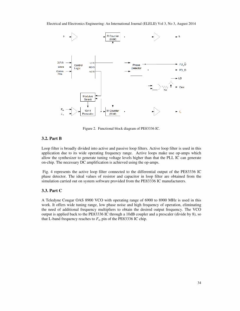
Peregrine’s PE83336 IC is a 44-pin, integer-N PLL chip which can synthesis up to 3.0 GHz. The
IC consists of a phase detector, counters, prescaler and control logic as shown in Figure. 2. The
modulus prescaler divides the VCO frequency by either 10 or 11. Counters “M” and “R” divide
the Fin and reference frequency, respectively, by integer values stored in register. The phase
frequency detector generates down and up frequency control signals [7]. Data can be written via
parallel bus, series bus, or hardwired direct to the pins. The direct hardwire is chosen in our
application as it provides the flexibility to avoid external processer which was required in serial or
parallel bus. The circuit realization using PE83336 is shown in Figure. 3.
Electrical and Electronics Engineering: An International Journal (ELELIJ) Vol 3, No 3, August 2014
34
Figure 2. Functional block diagram of PE83336 IC.
3.2. Part B
Loop filter is broadly divided into active and passive loop filters. Active loop filter is used in this
application due to its wide operating frequency range. Active loops make use op-amps which
allow the synthesizer to generate tuning voltage levels higher than that the PLL IC can generate
on-chip. The necessary DC amplification is achieved using the op-amps.
Fig. 4 represents the active loop filter connected to the differential output of the PE83336 IC
phase detector. The ideal values of resistor and capacitor in loop filter are obtained from the
simulation carried out on system software provided from the PE83336 IC manufacturers.
3.3. Part C
A Teledyne Cougar OAS 8900 VCO with operating range of 6900 to 8900 MHz is used in this
work. It offers wide tuning range, low phase noise and high frequency of operation, eliminating
the need of additional frequency multipliers to obtain the desired output frequency. The VCO
output is applied back to the PE83336 IC through a 10dB coupler and a prescaler (divide by 8), so
that L-band frequency reaches to Fin pin of the PE83336 IC chip.

Electrical and Electronics Engineering: An International Journal (ELELIJ) Vol 3, No 3, August 2014
35
Figure 3. Circuit realization of phase detector (block A).
Figure 4. Circuit realization of loop filter (block B).

Electrical and Electronics Engineering: An International Journal (ELELIJ) Vol 3, No 3, August 2014
36
Figure 5. Circuit realization of VCO and Prescaler (block C).
4. RESULTS The proposed frequency synthesizer consists of the PE83336 chip integrated with phase detector
and programmable frequency divider, TCXO, VCO, loop filter and prescaler. The desired
technical requirements of the PLL frequency synthesizer are mentioned below in Table 1.
Specification value
Frequency Band X-band
Phase noise ≤ -80 dBc/Hz at 1 KHz offset
Spurious ≤ -50dBc
Harmonic suppression ≤ -30 dBc
Output Power 7 dBm (min)
reference frequency 22.8 MHz
Table 1 Desired Specification
The PLL phase noise deteriorates from the TCXO phase noise by the given equation (4)
PLL Phase Noise= Phase noise of TCXO +20 log (Fout/Fr ) (4)

Electrical and Electronics Engineering: An International Journal (ELELIJ) Vol 3, No 3, August 2014
37
Figure 6. Phase noise of TCXO
The TCXO phase noise is obtained from figure 6. The PLL phase noise of -37dBc/Hz at 100 Hz
is calculated from Equation (4) when Fr is taken 22.8MHz and fout at X-band. This phase noise
matches with the phase noise obtained practically as shown in figure (7).
The performance (phase noise) of the PLL discussed in this paper is at par with performance of
the recently developed PLLs. The Comparison in terms of Phase noise reported in this paper ( -
82.56 dBc/Hz @ 1 KHz at X-band ) with earlier developed PLL’s is given in the table below-
Publications(references) X-Band Phase noise @ 1KHz
[1] -71 dBc/Hz
[8] -50 dBc/Hz
[9] -80 dBc/Hz
[10] -92.67 dBc/Hz
[11] -103.96 dBc/Hz
[12] -106 dBc/Hz
Table 2 Phase noise of recently developed PLL models.
In this application, the image can be reconstructed if the Bit Error Rate in the received data is
better or equal to 1 ×10⁶. The phase noise of this developed PLL at X-Band seen in fig 7 is
sufficient for this purpose.

Electrical and Electronics Engineering: An International Journal (ELELIJ) Vol 3, No 3, August 2014
38
Figure 7. Phase noise of PLL
The X-band carrier from PLL synthesizer is multiplied by a frequency tripler (X3) and driven
through driver amplifier as per the application requirements in this work. Fig.8 and 9 shows the
output spectrum of the PLL synthesizer at Ka-band(X-band multiplied by X3).
5. CONCLUSION An analog PLL frequency synthesizer intended for carrier generation application at X and Ka-
band has been presented in this paper. Design and implementation of a Low Phase Noise carrier
generator using PLL synthesizer on RT-duroid 6010 substrate is implemented. An active loop
filter which provides wide operating range and better filtering is used here. This implemented
model shows frequency resolution of 5.8 MHz and the phase noise better than -81 dBc/Hz @
1kHz offset.

Electrical and Electronics Engineering: An International Journal (ELELIJ) Vol 3, No 3, August 2014
39
Figure 8. PLL frequency synthesizer output at Ka-band for measuring phase noise.
Figure 9. PLL frequency synthesizer output at Ka-band showing the spectral purity

Electrical and Electronics Engineering: An International Journal (ELELIJ) Vol 3, No 3, August 2014
40
Figure 10. Top view of low noise PLL synthesiser on RT-duroid6010 substrate
REFERENCES
[1]F. Kroupa, Phase Lock Loops and Frequency Synthesis, John Wiley, 2003.
[2]Yuanwang Yang, Jingye Cai, Liu Lianfu, “A Frequency Synthesis Structure in Radar Target Simulation
System with High Agility and Resolution Performance”, Microwave Conference Proceedings (CJMW),
2011 China-Japan Joint. 2011, pp. 1-4
[3]Piotr Matuszczak, Lukasz Kulas, Krzysztof Nyka “Low Cost Microwave X-Band Generator”,
Proceedings of the 2nd International Conference on Information Technology, ICIT 2010 • 28-30 June
2010,Gdansk, Poland.
[4]F. Kroupa, Phase Lock Loops and Frequency Synthesis, John Wiley, 2003.
[5]P. V. Brennan, Phase-Locked Loops: Principle and Practice. New York: MacMillan, 1996.
[6]H. Komiya: The structure and design method of a high frequency PLL circuit”, CQ, 2009.
[7]Vabya Kumar Pandit, Chitra R, Sourabh Basu, Deepak V.Ingale, “Design and development of PLL
based X-band carrier generator for satellite applications”, International Journal of Science, Engineering and
Technology Research (IJSETR), Volume 3, Issue 3, March 2014
[8]Ja-Yol Lee, Kwidong Kim, Seung-Chul Lee, Jong-Kee Kwon, Jongdae Kim, Sang-Heung Le, “A 9.1-to-
11.5-GHz Four-Band PLL for X-Band Satellite & Optical Communication Applications”, Radio Frequency
Integrated Circuits IEEE,2007.
[9]Zhichao Wang, Miao Lin, Pinglian Wang: Lei Zhang Design and Implementation of X-Band Frequency
Synthesizer Based on ADF4156, High Speed Intelligent Communication Forum (HSIC), 2012 4th
International, 10-11 May 2012.
[10] Weibo Cui, Xiao Zhang, Xiao Lu, Yuxing Ren, Mingzhou Zhan, Bo Yan,“ The Design of High
Performance X-Band Frequency Synthesizer based on DDS and PLL”, CSQRWC 2013.
[11]Shengwu Yu, Jinping Xu, Zhihao Shen.” X-Band frequency synthesizer with high frequency
resolution”, 978-1-4673-0677-5/12 IEEE, 2012.
[12]XiaoHua Mu, Wen Liao, QingLin Huo, “ An X-Band frequency Synthesize with high Spurious
Suppression and Low Phase Noise”, 978-1-4673-2185-3/12 IEEE, 2012.

Electrical and Electronics Engineering: An International Journal (ELELIJ) Vol 3, No 3, August 2014
41
Authors Vabya Kumar Pandit, is a final year M.Tech, Scholar at Centre for Emerging
Technologies, Jain University, Bangalore, in the area of Radio Frequency
Communication. He completed B.E in Electronics and Tele-communications
Engineering, from Chhattisgarh Swami Vivekananda Technical University (CSVTU),
Bhilai in the year 2011. He has more than 4 papers to his credit which got published in
International journals.
Sourabh Basu, completed his bachelor’s degree in 2001 from Delhi University. He
completed Masters in Radio Frequency from Department of Electronic Science,
University of Delhi in the year 2005. Presently, he is working as a Scientist / Engineer in
Data Transmitter and Navigation Division of Communication Systems Group at ISRO
Satellite Centre, Bangalore. He has designed various RF modules for space applications.
Deepak V. Ingale, completed his M.Tech in VLSI and Embedded Systems in 2008.
Presently he is working as an Assistant Professor at Centre for Emerging Technologies,
Jain University, Bangalore. As a Project Engineer at Wipro Technologies he was
instrumental in component selection, board re-design(PCB), setting up & conducting
First Piece Evaluation(FPE) of various telecom switches and related activities. He has
more than 5 papers to his credit which got published in national and international
conferences/symposiums