Embed Size (px)
Citation preview
PLL Frequency Synthesizer DHL612
Nov. 2020 1/12 intochips inc. Copyright © 2016 intochips inc.
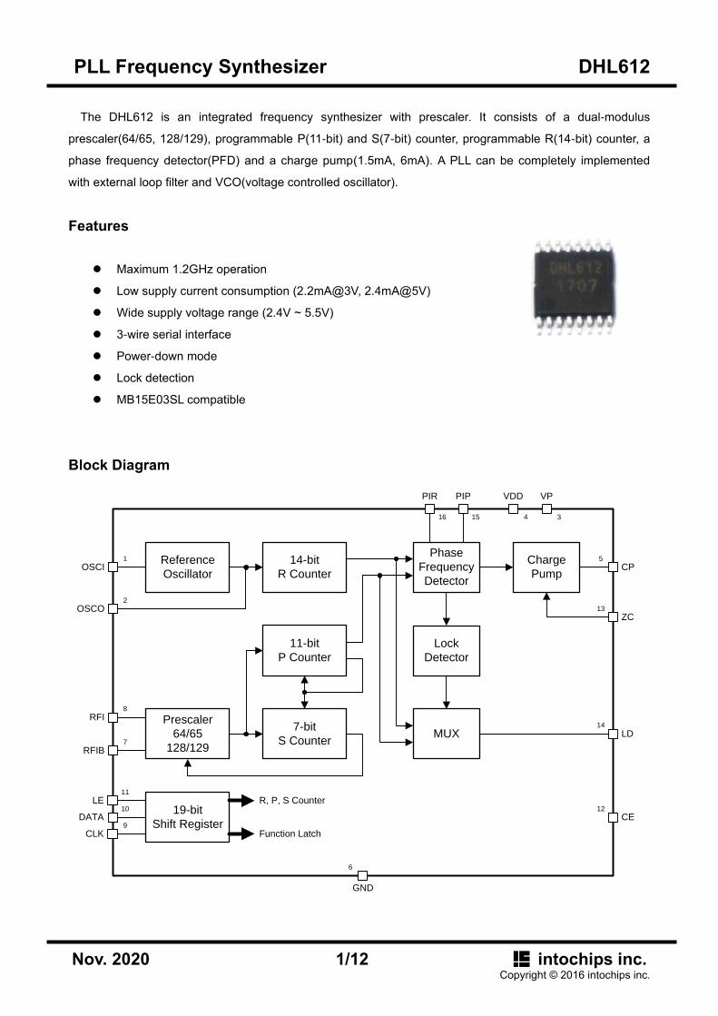
The DHL612 is an integrated frequency synthesizer with prescaler. It consists of a dual-modulus
prescaler(64/65, 128/129), programmable P(11-bit) and S(7-bit) counter, programmable R(14-bit) counter, a
phase frequency detector(PFD) and a charge pump(1.5mA, 6mA). A PLL can be completely implemented
with external loop filter and VCO(voltage controlled oscillator).
Features
Maximum 1.2GHz operation
Low supply current consumption (2.2mA@3V, 2.4mA@5V)
Wide supply voltage range (2.4V ~ 5.5V)
3-wire serial interface
Power-down mode
Lock detection
MB15E03SL compatible
Block Diagram
OSCI
OSCO
14-bit
R Counter
Prescaler
64/65
128/129
RFI
RFIB
11-bit
P Counter
7-bit
S Counter
Phase
Frequency
Detector
Charge
Pump
Lock
Detector
19-bit
Shift Register
LE
DATA
CLK
CE
MUX LD
R, P, S Counter
Function Latch
CP
PIR PIP VPVDD
GND
1
2
34
5
6
7
8
9
10
11
12
ZC13
14
1516
Reference
Oscillator

PLL Frequency Synthesizer DHL612
Nov. 2020 2/12 intochips inc. Copyright © 2016 intochips inc.
Pin Description
OSCI
OSCO
VP
VDD
CP
GND
RFIB
RFI
PIR
PIP
LD
ZC
CE
LE
DATA
CLK
1
2
3
4
5
6
7
8
16
15
14
13
12
11
10
9
Pin No. Mnemonic I/O Description
1 OSCI I Reference Oscillator input.
2 OSCO O Reference Oscillator output.
3 VP - Charge pump power supply.
4 VDD - Power supply.
5 CP O Charge pump output.
6 GND - Ground
7 RFIB I Complementary RF input.
A bypass capacitor should be placed to the ground plane.
8 RFI I RF input. This pin should be ac-coupled from the VCO
9 CLK I Serial clock input. (Do not open)
10 DATA I Serial data input. (Do not open)
11 LE I Serial data load enable. (Do not open)
12 CE I Chip Enable. (Do not open)
13 ZC I The charge pump output(CP) high-impedance control.
Internal pull-up resistor.
14 LD O Lock detect output(LDS=”L”) or Counter output(LDS=”H”).
15 PIP O Phase comparator N-channel open drain output for an external charge pump.
NMOS open drain output.
16 PIR O Phase comparator CMOS output for an external charge pump.

PLL Frequency Synthesizer DHL612
Nov. 2020 3/12 intochips inc. Copyright © 2016 intochips inc.
Absolute Maximum Ratings
Parameter Symbol Value Unit
Power Supply Voltage VDD -0.3 to 6.5 V
VP -0.3 to 6.5 V
Input/Output Voltage VIN, VOUT -0.3 to VDD+0.3 V
CP Output Voltage VCP -0.3 to VP+0.3 V
Storage Temperature Range TST -55 to +125 °C
ESD HBM (Human Body Model) VHBM 2000 V
MM (Machine Model) VMM 200 V
This device is a high performance RF integrated circuit and is ESD sensitive. Proper precautions should be taken for handling and
assembly.
Recommended Operating Conditions
Parameter Symbol Value Unit
Power Supply Voltage VDD 2.4 to 5.5 V
VP VDD to 5.5 V
Operating Temperature Range TOP -40 to +85 °C
PLL Frequency Synthesizer DHL612
Nov. 2020 4/12 intochips inc. Copyright © 2016 intochips inc.
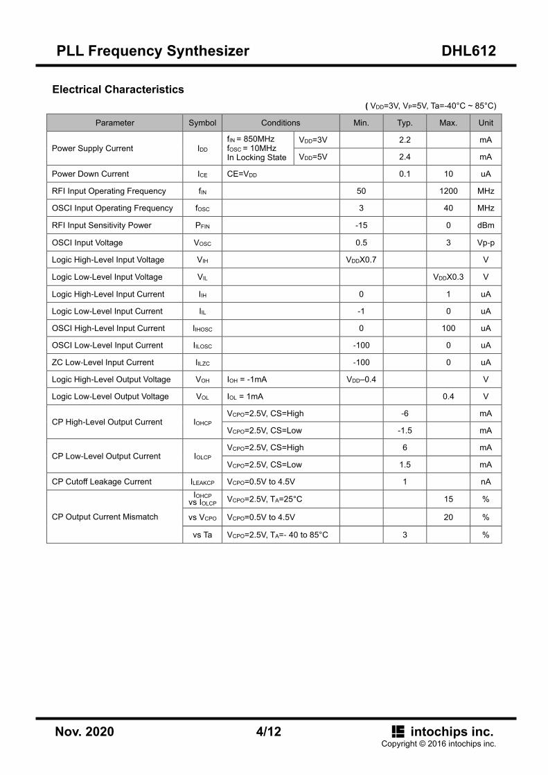
Electrical Characteristics
( VDD=3V, VP=5V, Ta=-40°C ~ 85°C)
Parameter Symbol Conditions Min. Typ. Max. Unit
Power Supply Current IDD fIN = 850MHz fOSC = 10MHz In Locking State
VDD=3V 2.2 mA
VDD=5V 2.4 mA
Power Down Current ICE CE=VDD 0.1 10 uA
RFI Input Operating Frequency fIN 50 1200 MHz
OSCI Input Operating Frequency fOSC 3 40 MHz
RFI Input Sensitivity Power PFIN -15 0 dBm
OSCI Input Voltage VOSC 0.5 3 Vp-p
Logic High-Level Input Voltage VIH VDDX0.7 V
Logic Low-Level Input Voltage VIL VDDX0.3 V
Logic High-Level Input Current IIH 0 1 uA
Logic Low-Level Input Current IIL -1 0 uA
OSCI High-Level Input Current IIHOSC 0 100 uA
OSCI Low-Level Input Current IILOSC -100 0 uA
ZC Low-Level Input Current IILZC -100 0 uA
Logic High-Level Output Voltage VOH IOH = -1mA VDD–0.4 V
Logic Low-Level Output Voltage VOL IOL = 1mA 0.4 V
CP High-Level Output Current IOHCP VCPO=2.5V, CS=High -6 mA
VCPO=2.5V, CS=Low -1.5 mA
CP Low-Level Output Current IOLCP VCPO=2.5V, CS=High 6 mA
VCPO=2.5V, CS=Low 1.5 mA
CP Cutoff Leakage Current ILEAKCP VCPO=0.5V to 4.5V 1 nA
CP Output Current Mismatch
IOHCP
vs IOLCP VCPO=2.5V, TA=25°C 15 %
vs VCPO VCPO=0.5V to 4.5V 20 %
vs Ta VCPO=2.5V, TA=- 40 to 85°C 3 %

PLL Frequency Synthesizer DHL612
Nov. 2020 5/12 intochips inc. Copyright © 2016 intochips inc.
Typical Performance Characteristics
RF Input Sensitivity vs Power Supply Voltage (64/65 mode)
RF Input Sensitivity Measurement Circuit
OSCI OSCO
1 2
16
VP
3
VDD
4
CP
5
GND
6
RFIB
7
RFI
8
PIR PIP LD ZC CE LE DATA CLK
15 14 13 12 11 10 9
100pF 100pF
10uF
10pF
0.1uF
VDD
10uF
10pF
0.1uF
VP
Signal
Generator
Controller
51Ω
Oscilloscope
-50
-40
-30
-20
-10
0
10
20
0 200 400 600 800 1000 1200 1400
RF
I In
pu
t P
ow
er
(dB
m)
RFI Input Frequency (MHz)
2.4 min.
2.4 max
3 min.
3 max
3.6 min.
3.6 max
5 min.
5 max
VDD (V)Ta=25oC

PLL Frequency Synthesizer DHL612
Nov. 2020 6/12 intochips inc. Copyright © 2016 intochips inc.
RF Input Sensitivity vs Temperature (64/65 mode)
Charge Pump Output Characteristics
-50
-40
-30
-20
-10
0
10
20
0 200 400 600 800 1000 1200 1400
RF
In
pu
t P
ow
er
(dB
m)
RFI Input Frequency (MHz)
VDD = 3V
85oC-40oC
max.
min.
-50
-40
-30
-20
-10
0
10
20
0 200 400 600 800 1000 1200 1400
RF
In
pu
t P
ow
er
(dB
m)
RFI Input Frequency (MHz)
VDD = 5V
85oC -40oC
max.
min.
-2
-1
0
1
2
0 1 2 3
Ch
arg
e P
um
p O
utp
ut C
urr
en
t (m
A)
Charge Pump Ouput Voltage (V)
IOHCP
IOLCPVDD=3VVP=3VTa=25oC
1.5mA mode
-8
-6
-4
-2
0
2
4
6
8
0 1 2 3
Ch
arg
e P
um
p O
utp
ut C
urr
en
t (m
A)
Charge Pump Ouput Voltage (V)
IOHCP
IOLCPVDD=3VVP=3VTa=25oC
6mA mode
-2
-1
0
1
2
0 1 2 3 4 5
Ch
arg
e P
um
p O
utp
ut C
urr
en
t (m
A)
Charge Pump Ouput Voltage (V)
IOHCP
IOLCPVDD=5VVP=5VTa=25oC
1.5mA mode
-8
-6
-4
-2
0
2
4
6
8
0 1 2 3 4 5
Cha
rge
Pu
mp
Ou
tpu
t C
urr
en
t (m
A)
Charge Pump Ouput Voltage (V)
IOHCP
IOLCPVDD=5VVP=5VTa=25oC
6mA mode
PLL Frequency Synthesizer DHL612
Nov. 2020 7/12 intochips inc. Copyright © 2016 intochips inc.
Power Supply Current Consumption
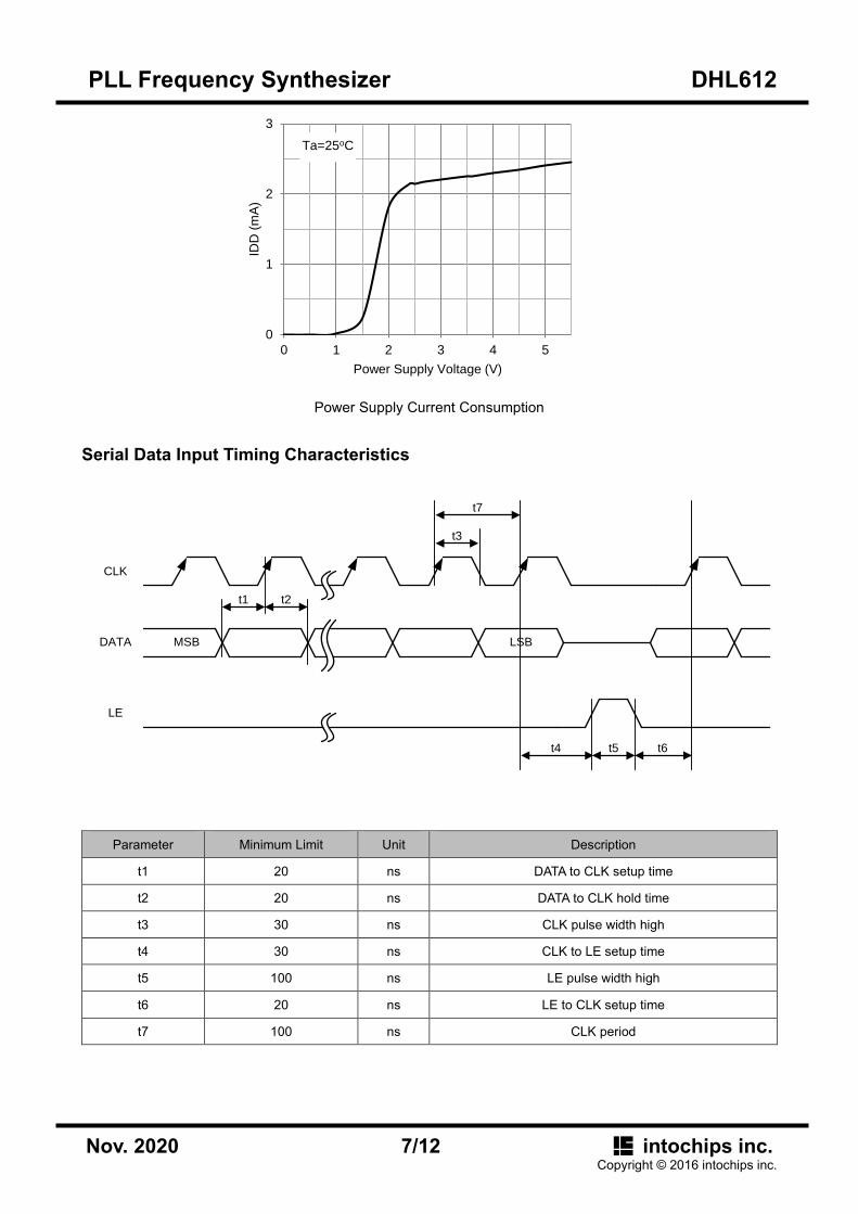
Serial Data Input Timing Characteristics
CLK
DATA
LE
MSB LSB
t5
t1
t3
t4
t7
t2
t6
Parameter Minimum Limit Unit Description
t1 20 ns DATA to CLK setup time
t2 20 ns DATA to CLK hold time
t3 30 ns CLK pulse width high
t4 30 ns CLK to LE setup time
t5 100 ns LE pulse width high
t6 20 ns LE to CLK setup time
t7 100 ns CLK period
0
1
2
3
0 1 2 3 4 5
IDD
(m
A)
Power Supply Voltage (V)
Ta=25oC
PLL Frequency Synthesizer DHL612
Nov. 2020 8/12 intochips inc. Copyright © 2016 intochips inc.
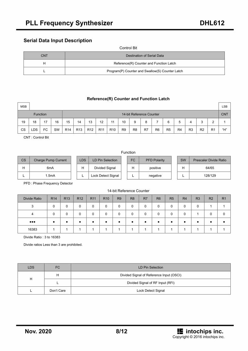
Serial Data Input Description
Control Bit
CNT Destination of Serial Data
H Reference(R) Counter and Function Latch
L Program(P) Counter and Swallow(S) Counter Latch
Reference(R) Counter and Function Latch
MSB LSB
Function 14-bit Reference Counter CNT
19 18 17 16 15 14 13 12 11 10 9 8 7 6 5 4 3 2 1
CS LDS FC SW R14 R13 R12 R11 R10 R9 R8 R7 R6 R5 R4 R3 R2 R1 “H”
CNT : Control Bit
Function
CS Charge Pump Current LDS LD Pin Selection FC PFD Polarity SW Prescaler Divide Ratio
H 6mA H Divided Signal H positive H 64/65
L 1.5mA L Lock Detect Signal L negative L 128/129
PFD : Phase Frequency Detector
14-bit Reference Counter
Divide Ratio R14 R13 R12 R11 R10 R9 R8 R7 R6 R5 R4 R3 R2 R1
3 0 0 0 0 0 0 0 0 0 0 0 0 1 1
4 0 0 0 0 0 0 0 0 0 0 0 1 0 0
16383 1 1 1 1 1 1 1 1 1 1 1 1 1 1
Divide Ratio : 3 to 16383
Divide ratios Less than 3 are prohibited.
LDS FC LD Pin Selection
H H Divided Signal of Reference Input (OSCI)
L Divided Signal of RF Input (RFI)
L Don’t Care Lock Detect Signal
PLL Frequency Synthesizer DHL612
Nov. 2020 9/12 intochips inc. Copyright © 2016 intochips inc.
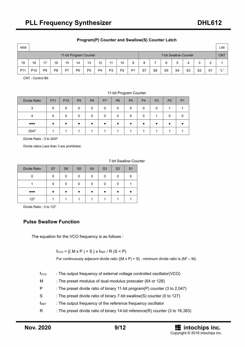
Program(P) Counter and Swallow(S) Counter Latch
MSB LSB
11-bit Program Counter 7-bit Swallow Counter CNT
19 18 17 16 15 14 13 12 11 10 9 8 7 6 5 4 3 2 1
P11 P10 P9 P8 P7 P6 P5 P4 P3 P2 P1 S7 S6 S5 S4 S3 S2 S1 “L”
CNT : Control Bit
11-bit Program Counter
Divide Ratio P11 P10 P9 P8 P7 P6 P5 P4 P3 P2 P1
3 0 0 0 0 0 0 0 0 0 1 1
4 0 0 0 0 0 0 0 0 1 0 0
2047 1 1 1 1 1 1 1 1 1 1 1
Divide Ratio : 3 to 2047
Divide ratios Less than 3 are prohibited.
7-bit Swallow Counter
Divide Ratio S7 S6 S5 S4 S3 S2 S1
0 0 0 0 0 0 0 0
1 0 0 0 0 0 0 1
127 1 1 1 1 1 1 1
Divide Ratio : 0 to 127
Pulse Swallow Function
The equation for the VCO frequency is as follows :
fVCO = ( M x P ) + S x fREF / R (S < P)
For continuously adjacent divide ratio (M x P) + S , minimum divide ratio is (M2 – M).
fVCO : The output frequency of external voltage controlled oscillator(VCO)
M : The preset modulus of dual-modulus prescaler (64 or 128)
P : The preset divide ratio of binary 11-bit program(P) counter (3 to 2,047)
S : The preset divide ratio of binary 7-bit swallow(S) counter (0 to 127)
fREF : The output frequency of the reference frequency oscillator
R : The preset divide ratio of binary 14-bit reference(R) counter (3 to 16,383)
PLL Frequency Synthesizer DHL612
Nov. 2020 10/12 intochips inc. Copyright © 2016 intochips inc.
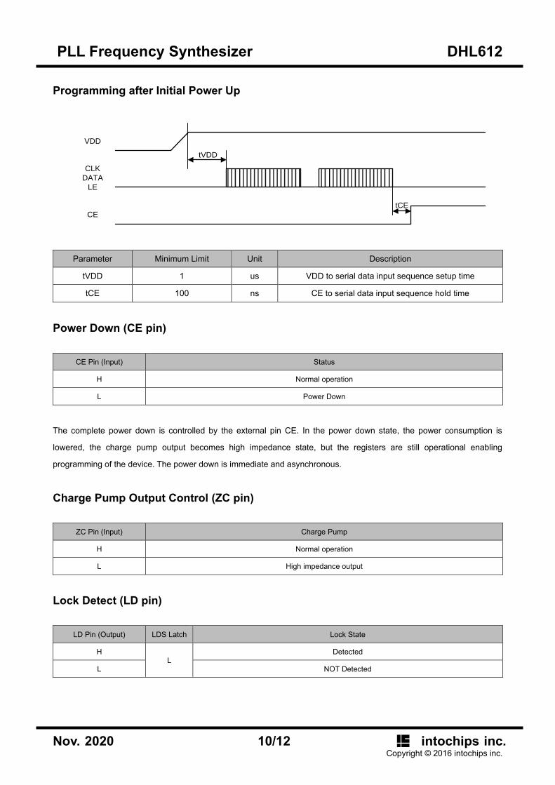
Programming after Initial Power Up
VDD
CLK
DATA
LE
tVDD
tCE
CE
Parameter Minimum Limit Unit Description
tVDD 1 us VDD to serial data input sequence setup time
tCE 100 ns CE to serial data input sequence hold time
Power Down (CE pin)
CE Pin (Input) Status
H Normal operation
L Power Down
The complete power down is controlled by the external pin CE. In the power down state, the power consumption is
lowered, the charge pump output becomes high impedance state, but the registers are still operational enabling
programming of the device. The power down is immediate and asynchronous.
Charge Pump Output Control (ZC pin)
ZC Pin (Input) Charge Pump
H Normal operation
L High impedance output
Lock Detect (LD pin)
LD Pin (Output) LDS Latch Lock State
H L
Detected
L NOT Detected

PLL Frequency Synthesizer DHL612
Nov. 2020 11/12 intochips inc. Copyright © 2016 intochips inc.
Crystal Oscillator Application using Reference Oscillator
OSCI1 2
OSCO
100KΩ
10MHz18pF 18pF
Reference Counter
Input
Reference Oscillator
The capacitor values need to be optimized to provide accurate matching between the crystal and the IC.
Application Example
OSCI OSCO
1 2
16
VP
3
VDD
4
CP
5
GND
6
RFIB
7
RFI
8
PIR PIP LD ZC CE LE DATA CLK
15 14 13 12 11 10 9
1000pF
TCXO
100pF 100pF
10uF
10pF
0.1uF
VDD
10uF
10pF
0.1uF
VP
Loop
FilterVCO
Controller

PLL Frequency Synthesizer DHL612
Nov. 2020 12/12 intochips inc. Copyright © 2016 intochips inc.
Package Dimensions
1 8
16
6.55
9
6.25
5.1
4.9
1.20 MAX
0.30
0.19
4.50
4.30
0.15
0.05
0.75
0o – 8
o 1.00 MAX
16 Pin TSSOP
0.45
0.20
0.09
0.65
Disclaimer
Intochips reserves the right to make changes without notice the design and processes for improving performance.
Intochips makes no warranty, representation or guarantee regarding the suitability of its products for any particular
purpose, nor does Intochips assume any liability arising out of the application or use of any product or circuit, and
specifically disclaims any and all liability, including without limitation consequential or incidental damages. Intochips
disclaims any and all implied warranties, including warranties of fitness for particular purpose, non-infringement and
merchantability. Intochips does not convey any license under its patent rights nor the rights of others.
Intochips products are not designed for use in medical, life-saving, or life-sustaining applications or for any other
application in which the failure of the Intochips product could result in personal injury or death. Customers using or
selling Intochips products do so at their own risk.