Embed Size (px)
Citation preview

PLL Frequency Synthesizer Data Sheet ADF4106 FEATURES 6.0 GHz bandwidth 2.7 V to 3.3 V power supply Separate charge pump supply (VP) allows extended
tuning voltage in 3 V systems Programmable dual-modulus prescaler
8/9, 16/17, 32/33, 64/65 Programmable charge pump currents Programmable antibacklash pulse width 3-wire serial interface Analog and digital lock detect Hardware and software power-down mode
APPLICATIONS Broadband wireless access Satellite systems Instrumentation Wireless LANS Base stations for wireless radios
GENERAL DESCRIPTION
The ADF4106 frequency synthesizer can be used to implement local oscillators in the up-conversion and down-conversion sections of wireless receivers and transmitters. It consists of a low noise, digital phase frequency detector (PFD), a precision charge pump, a programmable reference divider, programmable A counter and B counter, and a dual-modulus prescaler (P/P + 1). The A (6-bit) counter and B (13-bit) counter, in conjunction with the dual-modulus prescaler (P/P + 1), implement an N divider (N = BP + A). In addition, the 14-bit reference counter (R Counter) allows selectable REFIN frequencies at the PFD input. A complete phase-locked loop (PLL) can be implemented if the synthesizer is used with an external loop filter and voltage controlled oscillator (VCO). Its very high bandwidth means that frequency doublers can be eliminated in many high frequency systems, simplifying system architecture and reducing cost.
FUNCTIONAL BLOCK DIAGRAM
0272
0-00
1
CLKDATA
LE
REFIN
RFINARFINB
24-BIT INPUTREGISTER
SDOUT
AVDD DVDD
CE AGND DGND
14-BITR COUNTER
R COUNTERLATCH
22
14
FUNCTIONLATCH
A, B COUNTERLATCHFROM
FUNCTIONLATCH
PRESCALERP/P + 1
N = BP + A
LOAD
LOAD
13-BITB COUNTER
6-BITA COUNTER
6
19
13
M3 M2 M1
MUX
SDOUT
AVDD
HIGH Z
MUXOUT
CPGND RSETVP
CPPHASE
FREQUENCYDETECTOR
LOCKDETECT
REFERENCE
CHARGEPUMP
CURRENTSETTING 1
ADF4106
CPI3 CPI2 CPI1 CPI6 CPI5 CPI4
CURRENTSETTING 2
Figure 1.
Rev. F Document Feedback Information furnished by Analog Devices is believed to be accurate and reliable. However, no responsibility is assumed by Analog Devices for its use, nor for any infringements of patents or other rights of third parties that may result from its use. Specifications subject to change without notice. No license is granted by implication or otherwise under any patent or patent rights of Analog Devices. Trademarks and registered trademarks are the property of their respective owners.
One Technology Way, P.O. Box 9106, Norwood, MA 02062-9106, U.S.A. Tel: 781.329.4700 ©2001–2015 Analog Devices, Inc. All rights reserved. Technical Support www.analog.com
ADF4106 Data Sheet
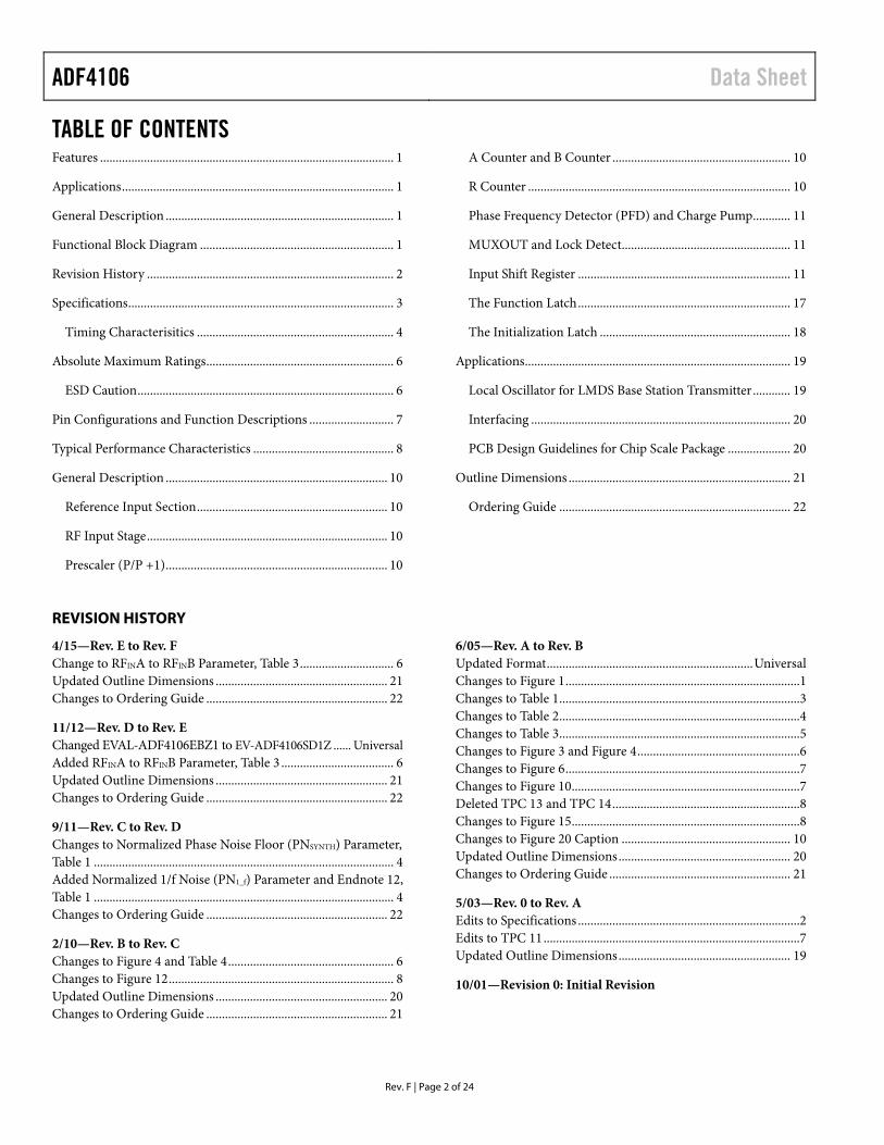
TABLE OF CONTENTS Features .............................................................................................. 1
Applications ....................................................................................... 1
General Description ......................................................................... 1
Functional Block Diagram .............................................................. 1
Revision History ............................................................................... 2
Specifications ..................................................................................... 3
Timing Characterisitics ............................................................... 4
Absolute Maximum Ratings ............................................................ 6
ESD Caution .................................................................................. 6
Pin Configurations and Function Descriptions ........................... 7
Typical Performance Characteristics ............................................. 8
General Description ....................................................................... 10
Reference Input Section ............................................................. 10
RF Input Stage ............................................................................. 10
Prescaler (P/P +1) ....................................................................... 10
A Counter and B Counter ......................................................... 10
R Counter .................................................................................... 10
Phase Frequency Detector (PFD) and Charge Pump ............ 11
MUXOUT and Lock Detect ...................................................... 11
Input Shift Register .................................................................... 11
The Function Latch .................................................................... 17
The Initialization Latch ............................................................. 18
Applications ..................................................................................... 19
Local Oscillator for LMDS Base Station Transmitter ............ 19
Interfacing ................................................................................... 20
PCB Design Guidelines for Chip Scale Package .................... 20
Outline Dimensions ....................................................................... 21
Ordering Guide .......................................................................... 22
REVISION HISTORY
4/15—Rev. E to Rev. F Change to RFINA to RFINB Parameter, Table 3 .............................. 6 Updated Outline Dimensions ....................................................... 21 Changes to Ordering Guide .......................................................... 22
11/12—Rev. D to Rev. E Changed EVAL-ADF4106EBZ1 to EV-ADF4106SD1Z ...... Universal Added RFINA to RFINB Parameter, Table 3 .................................... 6 Updated Outline Dimensions ....................................................... 21 Changes to Ordering Guide .......................................................... 22
9/11—Rev. C to Rev. D Changes to Normalized Phase Noise Floor (PNSYNTH) Parameter, Table 1 ................................................................................................ 4 Added Normalized 1/f Noise (PN1_f) Parameter and Endnote 12, Table 1 ................................................................................................ 4 Changes to Ordering Guide .......................................................... 22
2/10—Rev. B to Rev. C Changes to Figure 4 and Table 4 ..................................................... 6 Changes to Figure 12 ........................................................................ 8 Updated Outline Dimensions ....................................................... 20 Changes to Ordering Guide .......................................................... 21
6/05—Rev. A to Rev. B Updated Format .................................................................. Universal Changes to Figure 1 ........................................................................... 1 Changes to Table 1 ............................................................................. 3 Changes to Table 2 ............................................................................. 4 Changes to Table 3 ............................................................................. 5 Changes to Figure 3 and Figure 4 .................................................... 6 Changes to Figure 6 ........................................................................... 7 Changes to Figure 10 ......................................................................... 7 Deleted TPC 13 and TPC 14 ............................................................ 8 Changes to Figure 15 ......................................................................... 8 Changes to Figure 20 Caption ...................................................... 10 Updated Outline Dimensions ....................................................... 20 Changes to Ordering Guide .......................................................... 21
5/03—Rev. 0 to Rev. A Edits to Specifications ....................................................................... 2 Edits to TPC 11 .................................................................................. 7 Updated Outline Dimensions ....................................................... 19
10/01—Revision 0: Initial Revision
Rev. F | Page 2 of 24

Data Sheet ADF4106
SPECIFICATIONS AVDD = DVDD = 3 V ± 10%, AVDD ≤ VP ≤ 5.5 V, AGND = DGND = CPGND = 0 V, RSET = 5.1 kΩ, dBm referred to 50 Ω, TA = TMAX to TMIN, unless otherwise noted.
Table 1. Parameter B Version1 B Chips2 (typ) Unit Test Conditions/Comments RF CHARACTERISTICS See Figure 18 for input circuit
RF Input Frequency (RFIN) 0.5/6.0 0.5/6.0 GHz min/max For lower frequencies, ensure slew rate (SR) > 320 V/µs
RF Input Sensitivity –10/0 –10/0 dBm min/max Maximum Allowable Prescaler Output Frequency3
300 300 MHz max P = 8
325 325 MHz max P = 16 REFIN CHARACTERISTICS
REFIN Input Frequency 20/300 20/300 MHz min/max For f < 20 MHz, ensure SR > 50 V/µs REFIN Input Sensitivity4 0.8/VDD 0.8/VDD V p-p min/max Biased at AVDD/2 (see Note 55) REFIN Input Capacitance 10 10 pF max REFIN Input Current ±100 ±100 µA max
PHASE DETECTOR Phase Detector Frequency6 104 104 MHz max ABP = 0, 0 (2.9 ns antibacklash pulse width)
CHARGE PUMP Programmable, see Table 9 ICP Sink/Source
High Value 5 5 mA typ With RSET = 5.1 kΩ Low Value 625 625 µA typ Absolute Accuracy 2.5 2.5 % typ With RSET = 5.1 kΩ RSET Range 3.0/11 3.0/11 kΩ typ See Table 9
ICP Three-State Leakage 2 2 nA max 1 nA typical; TA = 25°C Sink and Source Current Matching 2 2 % typ 0.5 V ≤ VCP ≤ VP − 0.5 V
ICP vs. VCP 1.5 1.5 % typ 0.5 V ≤ VCP ≤ VP − 0.5 V ICP vs. Temperature 2 2 % typ VCP = VP/2
LOGIC INPUTS VIH, Input High Voltage 1.4 1.4 V min VIL, Input Low Voltage 0.6 0.6 V max IINH, IINL, Input Current ±1 ±1 µA max CIN, Input Capacitance 10 10 pF max
LOGIC OUTPUTS VOH, Output High Voltage 1.4 1.4 V min Open-drain output chosen, 1 kΩ pull-up
resistor to 1.8 V VOH, Output High Voltage VDD − 0.4 VDD − 0.4 V min CMOS output chosen IOH 100 100 µA max VOL, Output Low Voltage 0.4 0.4 V max IOL = 500 µA
POWER SUPPLIES AVDD 2.7/3.3 2.7/3.3 V min/V max DVDD AVDD AVDD VP AVDD/5.5 AVDD/5.5 V min/V max AVDD ≤ VP ≤ 5.5V IDD
7 (AIDD + DIDD) 11 9.0 mA max 9.0 mA typ IDD
8 (AIDD + DIDD) 11.5 9.5 mA max 9.5 mA typ IDD
9 (AIDD + DIDD) 13 10.5 mA max 10.5 mA typ IP 0.4 0.4 mA max TA = 25°C Power-Down Mode10
(AIDD + DIDD) 10 10 µA typ
Rev. F | Page 3 of 24

ADF4106 Data Sheet
Parameter B Version1 B Chips2 (typ) Unit Test Conditions/Comments NOISE CHARACTERISTICS
Normalized Phase Noise Floor (PNSYNTH)11
–223 –223 dBc/Hz typ PLL loop B/W = 500 kHz, measured at 100 kHz offset
Normalized 1/f Noise (PN1_f)12 −122 −122 dBc/Hz typ 10 kHz offset; normalized to 1 GHz Phase Noise Performance13 @ VCO output
900 MHz14 –92.5 −92.5 dBc/Hz typ @ 1 kHz offset and 200 kHz PFD frequency 5800 MHz15 −76.5 −76.5 dBc/Hz typ @ 1 kHz offset and 200 kHz PFD frequency 5800 MHz16 −83.5 −83.5 dBc/Hz typ @ 1 kHz offset and 1 MHz PFD frequency
Spurious Signals 900 MHz14 –90/–92 –90/–92 dBc typ @ 200 kHz/400 kHz and 200 kHz PFD frequency 5800 MHz15 –65/–70 –65/–70 dBc typ @ 200 kHz/400 kHz and 200 kHz PFD frequency 5800 MHz16 –70/–75 –70/–75 dBc typ @ 1 MHz/2 MHz and 1 MHz PFD frequency
1 Operating temperature range (B Version) is –40°C to +85°C. 2 The B chip specifications are given as typical values. 3 This is the maximum operating frequency of the CMOS counters. The prescaler value should be chosen to ensure that the RF input is divided down to a frequency that
is less than this value. 4 AVDD = DVDD = 3 V. 5 AC coupling ensures AVDD/2 bias. 6 Guaranteed by design. Sample tested to ensure compliance. 7 TA = 25°C; AVDD = DVDD = 3 V; P = 16; RFIN = 900 MHz. 8 TA = 25°C; AVDD = DVDD = 3 V; P = 16; RFIN = 2.0 GHz. 9 TA = 25°C; AVDD = DVDD = 3 V; P = 32; RFIN = 6.0 GHz. 10 TA = 25°C; AVDD = DVDD = 3.3 V; R = 16383; A = 63; B = 891; P = 32; RFIN = 6.0 GHz. 11 The synthesizer phase noise floor is estimated by measuring the in-band phase noise at the output of the VCO and subtracting 20 log N (where N is the N divider
value) and 10 log FPFD. PNSYNTH = PNTOT − 10 log FPFD − 20 log N. 12 The PLL phase noise is composed of 1/f (flicker) noise plus the normalized PLL noise floor. The formula for calculating the 1/f noise contribution at an RF frequency, fRF,
and at a frequency offset, f, is given by PN = PN1_f + 10 log(10 kHz/f) + 20 log(fRF/1 GHz). Both the normalized phase noise floor and flicker noise are modeled in ADIsimPLL.
13 The phase noise is measured with the EV-ADF4106SD1Z evaluation board and the Agilent E4440A Spectrum Analyzer. The spectrum analyzer provides the REFIN for the synthesizer (fREFOUT = 10 MHz @ 0 dBm).
14 fREFIN = 10 MHz; fPFD = 200 kHz; Offset Frequency = 1 kHz; fRF = 900 MHz; N = 4500; Loop B/W = 20 kHz. 15 fREFIN = 10 MHz; fPFD = 200 kHz; Offset Frequency = 1 kHz; fRF = 5800 MHz; N = 29000; Loop B/W = 20 kHz. 16 fREFIN = 10 MHz; fPFD = 1 MHz; Offset Frequency = 1 kHz; fRF = 5800 MHz; N = 5800; Loop B/W = 100 kHz.
TIMING CHARACTERISITICS AVDD = DVDD = 3 V ± 10%, AVDD ≤ VP ≤ 5.5 V, AGND = DGND = CPGND = 0 V, RSET = 5.1 kΩ, dBm referred to 50 Ω, TA = TMAX to TMIN, unless otherwise noted.
Table 2. Parameter Limit1 (B Version) Unit Test Conditions/Comments t1 10 ns min DATA to CLOCK Setup Time t2 10 ns min DATA to CLOCK Hold Time t3 25 ns min CLOCK High Duration t4 25 ns min CLOCK Low Duration t5 10 ns min CLOCK to LE Setup Time t6 20 ns min LE Pulse Width
1 Operating temperature range (B Version) is –40°C to +85°C.
Rev. F | Page 4 of 24

Data Sheet ADF4106
Rev. F | Page 5 of 24
0272
0-00
2
CLOCK
DB22 DB2DATA
LE
t1
LE
DB23 (MSB)
t2
DB1 (CONTROLBIT C2)
DB0 (LSB)(CONTROL BIT C1)
t3 t4
t6
t5
Figure 2. Timing Diagram
ADF4106 Data Sheet
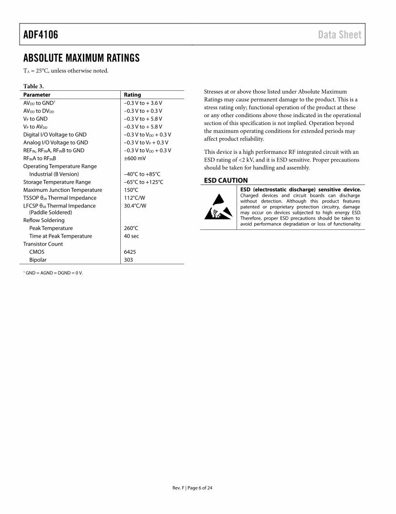
ABSOLUTE MAXIMUM RATINGS TA = 25°C, unless otherwise noted.
Table 3. Parameter Rating AVDD to GND1 –0.3 V to + 3.6 V AVDD to DVDD –0.3 V to + 0.3 V VP to GND –0.3 V to + 5.8 V VP to AVDD –0.3 V to + 5.8 V Digital I/O Voltage to GND –0.3 V to VDD + 0.3 V Analog I/O Voltage to GND –0.3 V to VP + 0.3 V REFIN, RFINA, RFINB to GND –0.3 V to VDD + 0.3 V RFINA to RFINB ±600 mV Operating Temperature Range
Industrial (B Version) –40°C to +85°C Storage Temperature Range –65°C to +125°C Maximum Junction Temperature 150°C TSSOP θJA Thermal Impedance 112°C/W LFCSP θJA Thermal Impedance
(Paddle Soldered) 30.4°C/W
Reflow Soldering Peak Temperature 260°C Time at Peak Temperature 40 sec
Transistor Count CMOS 6425 Bipolar 303
1 GND = AGND = DGND = 0 V.
Stresses at or above those listed under Absolute Maximum Ratings may cause permanent damage to the product. This is a stress rating only; functional operation of the product at these or any other conditions above those indicated in the operational section of this specification is not implied. Operation beyond the maximum operating conditions for extended periods may affect product reliability.
This device is a high performance RF integrated circuit with an ESD rating of <2 kV, and it is ESD sensitive. Proper precautions should be taken for handling and assembly.
ESD CAUTION
Rev. F | Page 6 of 24

Data Sheet ADF4106
PIN CONFIGURATIONS AND FUNCTION DESCRIPTIONS
0272
0-00
3
RSET
CP
CPGND
AGND
1
2
3
4
5
6
7
8
RFINB
RFINA
AVDD
REFIN
MUXOUT
LE
DATA
CLK
CE
DGND
16
15
14
13
12
11
10
9
VP
DVDD
TOP VIEW(Not to Scale)
ADF4106
NOTE: TRANSISTOR COUNT 6425 (CMOS),303 (BIPOLAR).
Figure 3. 16-Lead TSSOP Pin Configuration
0272
0-00
4
141312
1
34
LE15 MUXOUT
DATACLK
11 CE
CPGND
AGND2AGND
RFINB5RFINA
7A
V DD
6A
V DD
8R
EFIN
9D
GN
D10
DG
ND
19R
SET
20C
P
18V P
17D
V DD
16D
V DD
ADF4106TOP VIEW
(Not to Scale)
NOTES1. TRANSISTOR COUNT 6425 (CMOS),
303 (BIPOLAR).2. THE EXPOSED PAD MUST BE
CONNECTED TO AGND.
Figure 4. 20-Lead LFCSP_WQ Pin Configuration
Table 4. Pin Function Descriptions Pin No. TSSOP
Pin No. LFCSP Mnemonic Function
1 19 RSET Connecting a resistor between this pin and CPGND sets the maximum charge pump output current. The nominal voltage potential at the RSET pin is 0.66 V. The relationship between ICP and RSET is
SETMAXCP R
I 5.25=
So, with RSET = 5.1 kΩ, ICP MAX = 5 mA. 2 20 CP Charge Pump Output. When enabled, this provides ±ICP to the external loop filter, which in turn
drives the external VCO. 3 1 CPGND Charge Pump Ground. This is the ground return path for the charge pump. 4 2, 3 AGND Analog Ground. This is the ground return path of the prescaler. 5 4 RFINB Complementary Input to the RF Prescaler. This point must be decoupled to the ground plane with
a small bypass capacitor, typically 100 pF. See Figure 18. 6 5 RFINA Input to the RF Prescaler. This small signal input is ac-coupled to the external VCO. 7 6, 7 AVDD Analog Power Supply. This may range from 2.7 V to 3.3 V. Decoupling capacitors to the analog ground
plane should be placed as close as possible to this pin. AVDD must be the same value as DVDD. 8 8 REFIN Reference Input. This is a CMOS input with a nominal threshold of VDD/2 and a dc equivalent input
resistance of 100 kΩ. See Figure 18. This input can be driven from a TTL or CMOS crystal oscillator or it can be ac-coupled.
9 9, 10 DGND Digital Ground. 10 11 CE Chip Enable. A logic low on this pin powers down the device and puts the charge pump output
into three-state mode. Taking the pin high powers up the device, depending on the status of the power-down bit, F2.
11 12 CLK Serial Clock Input. This serial clock is used to clock in the serial data to the registers. The data is latched into the 24-bit shift register on the CLK rising edge. This input is a high impedance CMOS input.
12 13 DATA Serial Data Input. The serial data is loaded MSB first with the two LSBs being the control bits. This input is a high impedance CMOS input.
13 14 LE Load Enable, CMOS Input. When LE goes high, the data stored in the shift registers is loaded into one of the four latches with the latch being selected using the control bits.
14 15 MUXOUT This multiplexer output allows either the lock detect, the scaled RF, or the scaled reference frequency to be accessed externally.
15 16, 17 DVDD Digital Power Supply. This may range from 2.7 V to 3.3 V. Decoupling capacitors to the digital ground plane should be placed as close as possible to this pin. DVDD must be the same value as AVDD.
16 18 VP Charge Pump Power Supply. This should be greater than or equal to VDD. In systems where VDD is 3 V, it can be set to 5.5 V and used to drive a VCO with a tuning range of up to 5 V.
EP Exposed Pad. The exposed pad must be connected to AGND.
Rev. F | Page 7 of 24

ADF4106 Data Sheet
TYPICAL PERFORMANCE CHARACTERISTICS
0272
0-00
5
FREQ MAGS11 ANGS110.500 0.89148 –17.28200.600 0.88133 – 20.69190.700 0.87152 – 24.53860.800 0.85855 –27.32280.900 0.84911 –31.06981.000 0.83512 – 34.86231.100 0.82374 –38.55741.200 0.80871 –41.90931.300 0.79176 – 45.69901.400 0.77205 –49.41851.500 0.75696 –52.88981.600 0.74234 –56.29231.700 0.72239 –60.25841.800 0.69419 –63.14461.900 0.67288 –65.64642.000 0.66227 –68.07422.100 0.64758 –71.35302.200 0.62454 –75.56582.300 0.59466 –79.64042.400 0.55932 –82.82462.500 0.52256 –85.27952.600 0.48754 –85.62982.700 0.46411 –86.18542.800 0.45776 –86.49972.900 0.44859 –88.80803.000 0.44588 –91.97373.100 0.43810 –95.40873.200 0.43269 –99.1282
FREQ MAGS11 ANGS113.300 0.42777 –102.7483.400 0.42859 –107.1673.500 0.43365 –111.8833.600 0.43849 –117.5483.700 0.44475 –123.8563.800 0.44800 –130.3993.900 0.45223 –136.7444.000 0.45555 –142.7664.100 0.45313 –149.2694.200 0.45622 –154.8844.300 0.45555 –159.6804.400 0.46108 –164.9164.500 0.45325 –168.4524.600 0.45054 –173.4624.700 0.45200 –176.6974.800 0.45043 178.8244.900 0.45282 174.9475.000 0.44287 170.2375.100 0.44909 166.6175.200 0.44294 162.7865.300 0.44558 158.7665.400 0.45417 153.1955.500 0.46038 147.7215.600 0.47128 139.7605.700 0.47439 132.6575.800 0.48604 125.7825.900 0.50637 121.1106.000 0.52172 115.400
FREQ UNIT GHz KEYWORD RPARAM TYPE S IMPEDANCE 50ΩDATA FORMAT MA
Figure 5. S-Parameter Data for the RF Input
0
–30
–5
–10
–25
–20
–15
0272
0-00
6
6543210RF INPUT FREQUENCY (GHz)
RF
INPU
T PO
WER
(dB
m)
VDD = 3VVP = 3V
TA = +85°C
TA = –40°C
TA = +25°C
Figure 6. Input Sensitivity
0
–100
–90
–80
–70
–60
–50
–40
–30
–20
–10
0272
0-00
7
–2kHz –1kHz 900MHz 1kHz 2kHzFREQUENCY
OU
TPU
T PO
WER
(dB
)
VDD = 3V, VP = 5VICP = 5mAPFD FREQUENCY = 200kHzLOOP BANDWIDTH = 20kHzRES BANDWIDTH = 10HzVIDEO BANDWIDTH = 10HzSWEEP = 1.9 SECONDSAVERAGES = 10
–93.0dBc/Hz
REF LEVEL = –14.3dBm
Figure 7. Phase Noise (900 MHz, 200 kHz, and 20 kHz)
–40
–140
–130
–120
–110
–100
–90
–80
–70
–60
–50
0272
0-00
8
100Hz 1MHzFREQUENCY OFFSET FROM 900MHz CARRIER
OU
TPU
T PO
WER
(dB
)
10dB/DIVRL = –40dBc/HzRMS NOISE = 0.36°
Figure 8. Integrated Phase Noise (900 MHz, 200 kHz, and 20 kHz)
0
–100
–90
–80
–70
–60
–50
–40
–30
–20
–10
0272
0-00
9
–400kHz –200kHz 900MHz 200kHz 400kHzFREQUENCY
OU
TPU
T PO
WER
(dB
)REF LEVEL = –14.0dBm
VDD = 3V, VP = 5VICP = 5mAPFD FREQUENCY = 200kHzLOOP BANDWIDTH = 20kHzRES BANDWIDTH = 1kHzVIDEO BANDWIDTH = 1kHzSWEEP = 2.5 SECONDSAVERAGES = 30
–91.0dBc/Hz
Figure 9. Reference Spurs (900 MHz, 200 kHz, and 20 kHz)
–83.5dBc/Hz
0
–100
–90
–80
–70
–60
–50
–40
–30
–20
–10
0272
0-01
0
–2kHz –1kHz 5800MHz 1kHz 2kHzFREQUENCY
OU
TPU
T PO
WER
(dB
)
REF LEVEL = –10dBm VDD = 3V, VP = 5VICP = 5mAPFD FREQUENCY = 1MHzLOOP BANDWIDTH = 100kHzRES BANDWIDTH = 10HzVIDEO BANDWIDTH = 10HzSWEEP = 1.9 SECONDSAVERAGES = 10
Figure 10. Phase Noise (5.8 GHz,1 MHz, and 100 kHz)
Rev. F | Page 8 of 24

Data Sheet ADF4106
–40
–140
–130
–120
–110
–100
–90
–80
–70
–60
–50
0272
0-01
1
100Hz 1MHzFREQUENCY OFFSET FROM 5800MHz CARRIER
PHA
SE N
OIS
E (d
Bc/
Hz)
10dB/DIVRL = –40dBc/HzRMS NOISE = 1.8°
Figure 11. Integrated Phase Noise (5.8 GHz,1 MHz, and 100 kHz)
0
–100
–90
–80
–70
–60
–50
–40
–30
–20
–10
0272
0-01
2
–2M –1M 5800 1M 2MFREQUENCY (Hz)
OU
TPU
T PO
WER
(dB
)
REF LEVEL = –10dBm
–65.0dBc–66.0dBc
VDD = 3V, VP = 5VICP = 5mAPFD FREQUENCY = 1MHzLOOP BANDWIDTH = 100kHzRES BANDWIDTH = 1kHzVIDEO BANDWIDTH = 1kHzSWEEP = 13 SECONDSAVERAGES = 1
Figure 12. Reference Spurs (5.8 GHz,1 MHz, and 100 kHz)
–60
–100
–90
–80
–70
0272
0-01
3
100–40 –20 0 20 40 60 80TEMPERATURE (°C)
PHA
SE N
OIS
E (d
Bc/
Hz)
VDD = 3VVP = 3V
Figure 13. Phase Noise (5.8 GHz,1 MHz, and 100 kHz) vs. Temperature
–5
–105
–95
–85
–75
–65
–55
–45
–35
–25
–15
0272
0-01
4
50 1 2 3 4TUNNING VOLTAGE (V)
FIR
ST R
EFER
ENC
E SP
UR
(dB
c)
VDD = 3VVP = 5V
Figure 14. Reference Spurs vs. VTUNE (5.8 GHz,1 MHz, and 100 kHz)
–120
–180
–170
–160
–150
–140
–130
0272
0-01
5
100M10k 100k 1M 10MPHASE ETECTOR FREQUENCY (Hz)
PHA
SE N
OIS
E (d
Bc/
Hz)
VDD = 3VVP = 5V
Figure 15. Phase Noise (Referred to CP Output) vs. PFD Frequency
–6
6
5
4
3
2
1
0
–1
–2
–3
–4
–5
0272
0-01
6
5.00 0.5 1.0 1.5 2.0 2.5 3.0 3.5 4.0 4.5VCP (V)
I CP
(mA
)
VPP = 5VICP SETTLING = 5mA
Figure 16. Charge Pump Output Characteristics
Rev. F | Page 9 of 24

ADF4106 Data Sheet
Rev. F | Page 10 of 24
GENERAL DESCRIPTION REFERENCE INPUT SECTION The reference input stage is shown in Figure 17. SW1 and SW2 are normally closed switches. SW3 is a normally open switch. When power-down is initiated, SW3 is closed and SW1 and SW2 are opened. This ensures that there is no loading of the REFIN pin on power-down.
0272
0-01
7
100kNC
REFIN NC
NO
SW1
SW2
BUFFER
SW3
TO R COUNTER
POWER-DOWNCONTROL
Figure 17. Reference Input Stage
RF INPUT STAGE The RF input stage is shown in Figure 18. It is followed by a 2-stage limiting amplifier to generate the CML clock levels needed for the prescaler.
0272
0-01
8
500
1.6V
500
AGND
RFINA
RFINB
AVDDBIAS
GENERATOR
Figure 18. RF Input Stage
PRESCALER (P/P +1) The dual-modulus prescaler (P/P + 1), along with the A counter and B counter, enables the large division ratio, N, to be realized (N = BP + A). The dual-modulus prescaler, operating at CML levels, takes the clock from the RF input stage and divides it down to a manageable frequency for the CMOS A counter and B counter. The prescaler is programmable. It can be set in soft-ware to 8/9, 16/17, 32/33, or 64/65. It is based on a synchronous 4/5 core. There is a minimum divide ratio possible for fully contiguous output frequencies. This minimum is determined by P, the prescaler value, and is given by (P2 − P).
A COUNTER AND B COUNTER The A counter and B CMOS counter combine with the dual modulus prescaler to allow a wide ranging division ratio in the PLL feedback counter. The counters are specified to work when the prescaler output is 325 MHz or less. Thus, with an RF input frequency of 4.0 GHz, a prescaler value of 16/17 is valid, but a value of 8/9 is not valid.
Pulse Swallow Function
The A counter and B counter, in conjunction with the dual-modulus prescaler, make it possible to generate output frequencies that are spaced only by the reference frequency divided by R. The equation for the VCO frequency is
R
REFINfABPVCOf
where:
fVCO is the output frequency of the external voltage controlled oscillator (VCO).
P is the preset modulus of the dual-modulus prescaler (8/9, 16/17, etc.).
B is the preset divide ratio of the binary 13-bit counter (3 to 8191).
A is the preset divide ratio of the binary 6-bit swallow counter (0 to 63).
fREFIN is the external reference frequency oscillator.
LOADLOAD
FROM RFINPUT STAGE
PRESCALERP/P + 1
13-BIT BCOUNTER
TO PFD
6-BIT ACOUNTER
N DIVIDER
MODULUSCONTROL
N = BP + A
0272
0-01
9
Figure 19. A and B Counters
R COUNTER The 14-bit R counter allows the input reference frequency to be divided down to produce the reference clock to the phase frequency detector (PFD). Division ratios from 1 to 16,383 are allowed.

Data Sheet ADF4106
PHASE FREQUENCY DETECTOR (PFD) AND CHARGE PUMP The PFD takes inputs from the R counter and N counter (N = BP + A) and produces an output proportional to the phase and frequency difference between them. Figure 20 is a simplified schematic. The PFD includes a programmable delay element that controls the width of the antibacklash pulse. This pulse ensures that there is no dead zone in the PFD transfer function and minimizes phase noise and reference spurs. Two bits in the reference counter latch, ABP2 and ABP1, control the width of the pulse. See Table 7.
HI
HI
D1
D2
Q1
Q2CLR2
CP
U1
U2
UP
DOWN
ABP2 ABP1
CPGND
U3
R DIVIDER
PROGRAMMABLEDELAY
N DIVIDER
VPCHARGE
PUMP
0272
0-02
0
CLR1
Figure 20. PFD Simplified Schematic
MUXOUT AND LOCK DETECT The output multiplexer on the ADF4106 allows the user to access various internal points on the chip. The state of MUXOUT is controlled by M3, M2, and M1 in the function latch. Table 9 shows the full truth table. Figure 21 shows the MUXOUT section in block diagram form.
Lock Detect
MUXOUT can be programmed for two types of lock detect: digital lock detect and analog lock detect.
Digital lock detect is active high. When LDP in the R counter latch is set to 0, digital lock detect is set high when the phase error on three consecutive phase detector cycles is less than 15 ns. With LDP set to 1, five consecutive cycles of less than 15 ns are required to set the lock detect. It stays set high until a phase error of greater than 25 ns is detected on any subsequent PD cycle.
The N-channel, open-drain, analog lock detect should be operated with an external pull-up resistor of 10 kΩ nominal. When lock is detected, this output is high with narrow, low-going pulses.
0272
0-02
1
DGND
DVDD
CONTROLMUX
ANALOG LOCK DETECT
DIGITAL LOCK DETECT
R COUNTER OUTPUT
N COUNTER OUTPUT
SDOUT
MUXOUT
Figure 21. MUXOUT Circuit
INPUT SHIFT REGISTER The ADF4106 digital section includes a 24-bit input shift register, a 14-bit R counter, and a 19-bit N counter, comprising a 6-bit A counter and a 13-bit B counter. Data is clocked into the 24-bit shift register on each rising edge of CLK. The data is clocked in MSB first. Data is transferred from the shift register to one of four latches on the rising edge of LE. The destination latch is determined by the state of the two control bits (C2, C1) in the shift register. These are the two LSBs, DB1 and DB0, as shown in the timing diagram of Figure 2. The truth table for these bits is shown in Table 5. Table 6 shows a summary of how the latches are programmed.
Table 5. C1, C2 Truth Table Control Bits C2 C1 Data Latch 0 0 R Counter 0 1 N Counter (A and B) 1 0 Function Latch (Including Prescaler) 1 1 Initialization Latch
Rev. F | Page 11 of 24

ADF4106 Data Sheet Table 6. Latch Summary
DB20 DB19 DB18 DB17 DB16 DB15 DB14 DB13 DB12 DB11 DB10 DB9 DB8 DB7 DB6 DB5 DB4 DB3 DB2 DB1 DB0
C2 (0) C1 (0)R1R2R3R4R5R6R7R8R9R10R11R12R13R14ABP1ABP2T1T2LDP
DB21DB22DB23
0 0X
DB20 DB19 DB18 DB17 DB16 DB15 DB14 DB13 DB12 DB11 DB10 DB9 DB8 DB7 DB6 DB5 DB4 DB3 DB2 DB1 DB0
C2 (0) C1 (1)A1A2A3A4A5B1B2B3B4B5B6B7B8B9B10B11B12B13 A6
DB21DB22DB23
G1XX
DB20 DB19 DB18 DB17 DB16 DB15 DB14 DB13 DB12 DB11 DB10 DB9 DB8 DB7 DB6 DB5 DB4 DB3 DB2 DB1 DB0
C2 (1) C1 (0)F1PD1M1M2M3F3P1P2 CPI1CPI2CPI5CPI6 TC4PD2 F2CPI3CPI4
DB21
TC3 TC2 TC1
DB22DB23
F4F5
DB20 DB19 DB18 DB17 DB16 DB15 DB14 DB13 DB12 DB11 DB10 DB9 DB8 DB7 DB6 DB5 DB4 DB3 DB2 DB1 DB0
C2 (1) C1 (1)F1PD1M1M2M3F3P1P2 CPI1CPI2CPI5CPI6 TC4PD2 F2CPI3CPI4
DB21
TC3 TC2 TC1
DB22DB23
F4F5
REFERENCE COUNTER LATCH
RESERVED
LOC
KD
ETEC
TPR
ECIS
ION
TESTMODE BITS
ANTI-BACKLASH
WIDTH14-BIT REFERENCE COUNTER CONTROL
BITS
RESERVED 13-BIT B COUNTER 6-BIT A COUNTER CONTROLBITS
N COUNTER LATCH
CP
GA
IN
FUNCTION LATCH
PRESCALERVALUE
POW
ER-
DO
WN
2 CURRENTSETTING
2
CURRENTSETTING
1
TIMER COUNTERCONTROL
FAST
LOC
KM
OD
E
FAST
LOC
KEN
AB
LE
CP
THR
EE-
STA
TE
PDPO
LAR
ITY
MUXOUTCONTROL
POW
ER-
DO
WN
1
CO
UN
TER
RES
ET CONTROLBITS
PRESCALERVALUE
POW
ER-
DO
WN
2 CURRENTSETTING
2
CURRENTSETTING
1TIMER COUNTER
CONTROL
FAST
LOC
KM
OD
E
FAST
LOC
KEN
AB
LE
CP
THR
EE-
STA
TE
PDPO
LAR
ITY
MUXOUTCONTROL
POW
ER-
DO
WN
1
CO
UN
TER
RES
ET CONTROLBITS
INITIALIZATION LATCH
0272
0-02
2
Rev. F | Page 12 of 24

Data Sheet ADF4106 Table 7. Reference Counter Latch Map
LDP0
1
ABP2 ABP10 0 2.9ns0 1 1.3ns1 0 6.0ns1 1 2.9ns
R14 R13 R12 .......... R3 R2 R10 0 0 .......... 0 0 1 10 0 0 .......... 0 1 0 20 0 0 .......... 0 1 1 30 0 0 .......... 1 0 0 4. . . .......... . . . .. . . .......... . . . .. . . .......... . . . .1 1 1 .......... 1 0 0 163801 1 1 .......... 1 0 1 163811 1 1 .......... 1 1 0 163821 1 1 .......... 1 1 1 16383
X = DON’T CARE
DB20 DB19 DB18 DB17 DB16 DB15 DB14 DB13 DB12 DB11 DB10 DB9 DB8 DB7 DB6 DB5 DB4 DB3 DB2 DB1 DB0
C2 (0) C1 (0)R1R2R3R4R5R6R7R8R9R10R11R12R13R14ABP1ABP2T1T2LDP
DB21DB22DB23
0 0X
RESERVED LOC
KD
ETEC
TPR
ECIS
ION
TESTMODE BITS
ANTI-BACKLASH
WIDTH14-BIT REFERENCE COUNTER CONTROL
BITS
DIVIDE RATIO
ANTIBACKLASH PULSE WIDTH
TEST MODE BITSSHOULD BE SETTO 00 FOR NORMALOPERATION.
OPERATIONTHREE CONSECUTIVE CYCLES OF PHASE DELAY LESS THAN15ns MUST OCCUR BEFORE LOCK DETECT IS SET.FIVE CONSECUTIVE CYCLES OF PHASE DELAY LESS THAN15ns MUST OCCUR BEFORE LOCK DETECT IS SET.
BOTH OF THESE BITSMUST BE SET TO 0 FORNORMAL OPERATION.
0272
0-02
3
Rev. F | Page 13 of 24

ADF4106 Data Sheet Table 8. N (A, B) Counter Latch Map
DB20 DB19 DB18 DB17 DB16 DB15 DB14 DB13 DB12 DB11 DB10 DB9 DB8 DB7 DB6 DB5 DB4 DB3 DB2 DB1 DB0
C2 (0) C1 (1)A1A2A3A4A5B1B2B3B4B5B6B7B8B9B10B11B12B13 A6
DB21DB22DB23
G1
0 0
0 1
1 0
F4 (FUNCTION LATCH)FASTLOCK ENABLE
1 1
A6 A5 .......... A2 A10 0 .......... 0 0 00 0 .......... 0 1 10 0 .......... 1 0 20 0 .......... 1 1 3. . .......... . . .. . .......... . . .. . .......... . . .1 1 .......... 0 0 601 1 .......... 0 1 611 1 .......... 1 0 621 1 .......... 1 1 63
X X
B13 B12 B11 B3 B2 B1
0 0 0 .......... 0 0 00 0 0 .......... 0 0 10 0 0 .......... 0 1 00 0 0 .......... 0 1 1 3. . . .......... . . . .. . . .......... . . . .. . . .......... . . . .1 1 1 .......... 1 0 0 81881 1 1 .......... 1 0 1 81891 1 1 .......... 1 1 0 81901 1 1 .......... 1 1 1 8191
X = DON’T CARE
RESERVED 13-BIT B COUNTER 6-BIT A COUNTER CONTROLBITS
CP
GA
IN
A COUNTERDIVIDE RATIO
B COUNTER DIVIDE RATIO
NOT ALLOWEDNOT ALLOWEDNOT ALLOWED
THESE BITS ARE NOT USEDBY THE DEVICE AND AREDON'T CARE BITS.
OPERATIONCP GAINCHARGE PUMP CURRENTSETTING 1 IS PERMANENTLY USED.CHARGE PUMP CURRENTSETTING 2 IS PERMANENTLY USED.CHARGE PUMP CURRENTSETTING 1 IS USED.CHARGE PUMP CURRENT ISSWITCHED TO SETTING 2. THETIME SPENT IN SETTING 2 ISDEPENDENT ON WHICH FASTLOCKMODE IS USED. SEE FUNCTIONLATCH DESCRIPTION.
N = BP + A, P IS PRESCALER VALUE SET IN THE FUNCTIONLATCH. B MUST BE GREATER THAN OR EQUAL TO A. FORCONTINUOUSLY ADJACENT VALUES OF (N × FREF), AT THEOUTPUT, NMIN IS (P2 – P).
0272
0-02
4
Rev. F | Page 14 of 24

Data Sheet ADF4106 Table 9. Function Latch Map
P2 P10 0 8/90 1 16/171 0 32/331 1 64/65
PD2 PD1 MODE
0 X X1 X 01 0 11 1 1
CPI6 CPI5 CPI4CPI3 CPI2 CPI1 3kΩ 5.1kΩ 11kΩ0 0 0 1.06 0.625 0.2890 0 1 2.12 1.25 0.5800 1 0 3.18 1.875 0.8700 1 1 4.24 2.5 1.1601 0 0 5.30 3.125 1.4501 0 1 6.36 3.75 1.7301 1 0 7.42 4.375 2.0201 1 1 8.50 5.0 2.320
TC4 TC3 TC2 TC10 0 0 0 30 0 0 1 70 0 1 0 110 0 1 1 150 1 0 0 190 1 0 1 230 1 1 0 270 1 1 1 311 0 0 0 351 0 0 1 391 0 1 0 431 0 1 1 471 1 0 0 511 1 0 1 551 1 1 0 591 1 1 1 63
F4011
M3 M2 M10 0 00 0 1
0 1 00 1 11 0 01 0 1
1 1 01 1 1
F301
F201
F101
DB20 DB19 DB18 DB17 DB16 DB15 DB14 DB13 DB12 DB11 DB10 DB9 DB8 DB7 DB6 DB5 DB4 DB3 DB2 DB1 DB0
C2 (1) C1 (0)F1PD1M1M2M3F3P1P2 CPI1CPI2CPI5CPI6 TC4PD2 F2CPI3CPI4
DB21
TC3 TC2 TC1
DB22DB23
F4F5
F5X01
NEGATIVEPOSITIVE
PRESCALERVALUE
POW
ER-
DO
WN
2 CURRENTSETTING
2
CURRENTSETTING
1
TIMER COUNTERCONTROL
FAST
LOC
KM
OD
E
FAST
LOC
KEN
AB
LE
CP
THR
EE-
STA
TE MUXOUTCONTROL
POW
ER-
DO
WN
1
CO
UN
TER
RES
ET CONTROLBITS
PHASE DETECTORPOLARITY
COUNTEROPERATIONNORMALR, A, B COUNTERSHELD IN RESET
CHARGE PUMPOUTPUT
NORMALTHREE-STATE
FASTLOCK DISABLEDFASTLOCK MODE 1FASTLOCK MODE 2
FASTLOCK MODE
THREE-STATE OUTPUTDIGITAL LOCK DETECT(ACTIVE HIGH)N DIVIDER OUTPUTDVDDR DIVIDER OUTPUTN-CHANNEL OPEN-DRAINLOCK DETECTSERIAL DATA OUTPUTDGND
OUTPUTTIMEOUT(PFD CYCLES)
ICP (mA)
ASYNCHRONOUS POWER-DOWNNORMAL OPERATIONASYNCHRONOUS POWER-DOWNSYNCHRONOUS POWER-DOWN
CE PIN
PRESCALER VALUE
PDPO
LAR
ITY
0272
0-02
5
Rev. F | Page 15 of 24

ADF4106 Data Sheet Table 10. Initialization Latch Map
P2 P10 0 8/90 1 16/171 0 32/331 1 64/65
PD2 PD1 MODE
0 X X1 X 01 0 11 1 1
CPI6 CPI5 CPI4CPI3 CPI2 CPI1 3kΩ 5.1kΩ 11kΩ0 0 0 1.06 0.625 0.2890 0 1 2.12 1.25 0.5800 1 0 3.18 1.875 0.8700 1 1 4.24 2.5 1.1601 0 0 5.30 3.125 1.4501 0 1 6.36 3.75 1.7301 1 0 7.42 4.375 2.0201 1 1 8.50 5.0 2.320
TC4 TC3 TC2 TC10 0 0 0 30 0 0 1 70 0 1 0 110 0 1 1 150 1 0 0 190 1 0 1 230 1 1 0 270 1 1 1 311 0 0 0 351 0 0 1 391 0 1 0 431 0 1 1 471 1 0 0 511 1 0 1 551 1 1 0 591 1 1 1 63
F4011
M3 M2 M10 0 00 0 1
0 1 00 1 11 0 01 0 1
1 1 01 1 1
F301
F201
F101
DB20 DB19 DB18 DB17 DB16 DB15 DB14 DB13 DB12 DB11 DB10 DB9 DB8 DB7 DB6 DB5 DB4 DB3 DB2 DB1 DB0
C2 (1) C1 (1)F1PD1M1M2M3F3P1P2 CPI1CPI2CPI5CPI6 TC4PD2 F2CPI3CPI4
DB21
TC3 TC2 TC1
DB22DB23
F4F5
THREE-STATE
F5X01
NEGATIVEPOSITIVE
PRESCALERVALUE
POW
ER-
DO
WN
2 CURRENTSETTING
2
CURRENTSETTING
1
TIMER COUNTERCONTROL
FAST
LOC
KM
OD
E
FAST
LOC
KEN
AB
LE
CP
THR
EE-
STA
TE MUXOUTCONTROL
POW
ER-
DO
WN
1
CO
UN
TER
RES
ET CONTROLBITS
PHASE DETECTORPOLARITY
COUNTEROPERATIONNORMALR, A, B COUNTERSHELD IN RESET
CHARGE PUMPOUTPUTNORMAL
FASTLOCK DISABLEDFASTLOCK MODE 1FASTLOCK MODE 2
FASTLOCK MODE
THREE-STATE OUTPUTDIGITAL LOCK DETECT(ACTIVE HIGH)N DIVIDER OUTPUTDVDDR DIVIDER OUTPUTN-CHANNEL OPEN-DRAINLOCK DETECTSERIAL DATA OUTPUTDGND
OUTPUTTIMEOUT(PFD CYCLES)
ICP (mA)
ASYNCHRONOUS POWER-DOWNNORMAL OPERATIONASYNCHRONOUS POWER-DOWNSYNCHRONOUS POWER-DOWN
CE PIN
PRESCALER VALUE
PDPO
LAR
ITY
0272
0-02
6
Rev. F | Page 16 of 24
Data Sheet ADF4106
THE FUNCTION LATCH With C2 and C1 set to 1 and 0, respectively, the on-chip function latch is programmed. Table 9 shows the input data format for programming the function latch.
Counter Reset
DB2 (F1) is the counter reset bit. When this is 1, the R counter and the N (A, B) counter are reset. For normal operation, this bit should be 0. When powering up, disable the F1 bit (set to 0). The N counter will then resume counting in close alignment with the R counter. (The maximum error is one prescaler cycle).
Power-Down DB3 (PD1) and DB21 (PD2) provide programmable power-down modes. They are enabled by the CE pin.
When the CE pin is low, the device is immediately disabled regardless of the states of PD2, PD1.
In the programmed asynchronous power-down, the device powers down immediately after latching 1 into the PD1 bit, with the condition that PD2 is loaded with 0.
In the programmed synchronous power-down, the device power-down is gated by the charge pump to prevent unwanted frequency jumps. Once the power-down is enabled by writing 1 into the PD1 bit (provided that 1 has also been loaded to PD2), then the device goes into power-down during the next charge pump event.
When a power-down is activated (either synchronous or asynchronous mode, including CE pin activated power-down), the following events occur:
• All active dc current paths are removed.
• The R, N, and timeout counters are forced to their load state conditions.
• The charge pump is forced into three-state mode.
• The digital clock detect circuitry is reset.
• The RFIN input is debiased.
• The reference input buffer circuitry is disabled.
• The input register remains active and capable of loading and latching data.
MUXOUT Control
The on-chip multiplexer is controlled by M3, M2, and M1 on the ADF4106 family. Table 9 shows the truth table.
Fastlock Enable Bit
DB9 of the function latch is the fastlock enable bit. When this bit is 1, fastlock is enabled.
Fastlock Mode Bit
DB10 of the function latch is the fastlock mode bit. When fastlock is enabled, this bit determines which fastlock mode is used. If the fastlock mode bit is 0, then Fastlock Mode 1 is selected; and if the fastlock mode bit is 1, then Fastlock Mode 2 is selected.
Fastlock Mode 1
The charge pump current is switched to the contents of Current Setting 2. The device enters fastlock when 1 is written to the CP gain bit in the N (A, B) counter latch. The device exits fastlock when 0 is written to the CP gain bit in the N (A, B) counter latch.
Fastlock Mode 2
The charge pump current is switched to the contents of Current Setting 2. The device enters fastlock when 1 is written to the CP gain bit in the N (A, B) counter latch. The device exits fastlock under the control of the timer counter. After the timeout period, which is determined by the value in TC4 to TC1, the CP gain bit in the N (A, B) counter latch is automatically reset to 0, and the device reverts to normal mode instead of fastlock. See Table 9 for the timeout periods.
Timer Counter Control
The user has the option of programming two charge pump currents. The intent is that Current Setting 1 is used when the RF output is stable and the system is in a static state. Current Setting 2 is used when the system is dynamic and in a state of change (that is, when a new output frequency is programmed). The normal sequence of events follows.
The user initially decides what the preferred charge pump currents are going to be. For example, the choice may be 2.5 mA as Current Setting 1 and 5 mA as the Current Setting 2.
Simultaneously, the decision must be made as to how long the secondary current stays active before reverting to the primary current. This is controlled by the timer counter control bits, DB14 to DB11 (TC4 to TC1), in the function latch. The truth table is given in Table 9.
To program a new output frequency, simply program the N (A, B) counter latch with new values for A and B. Simultaneously, the CP gain bit can be set to 1, which sets the charge pump with the value in CPI6 to CPI4 for a period of time determined by TC4 to TC1. When this time is up, the charge pump current reverts to the value set by CPI3 to CPI1. At the same time, the CP gain bit in the N (A, B) counter latch is reset to 0 and is now ready for the next time the user wishes to change the frequency.
Note that there is an enable feature on the timer counter. It is enabled when Fastlock Mode 2 is chosen by setting the fastlock mode bit (DB10) in the function latch to 1.
Rev. F | Page 17 of 24

ADF4106 Data Sheet Charge Pump Currents
CPI3, CPI2, and CPI1 program Current Setting 1 for the charge pump. CPI6, CPI5, and CPI4 program Current Setting 2 for the charge pump. The truth table is given in Table 9.
Prescaler Value
P2 and P1 in the function latch set the prescaler values. The prescaler value should be chosen so that the prescaler output frequency is always less than or equal to 325 MHz. Therefore, with an RF frequency of 4 GHz, a prescaler value of 16/17 is valid, but a value of 8/9 is not valid.
PD Polarity
This bit sets the phase detector polarity bit. See Table 9.
CP Three-State
This bit controls the CP output pin. With the bit set high, the CP output is put into three-state. With the bit set low, the CP output is enabled.
THE INITIALIZATION LATCH When C2 and C1 = 1 and 1, respectively, the initialization latch is programmed. This is essentially the same as the function latch (programmed when C2 and C1 = 1 and 0, respectively).
However, when the initialization latch is programmed, there is an additional internal reset pulse applied to the R and N (A, B) counters. This pulse ensures that the N (A, B) counter is at the load point when the N (A, B) counter data is latched and the device begins counting in close phase alignment.
If the latch is programmed for synchronous power-down (CE pin is high, PD1 bit is high, and PD2 bit is low), the internal pulse also triggers this power-down. The prescaler reference and the oscillator input buffer are unaffected by the internal reset pulse; therefore, close phase alignment is maintained when counting resumes.
When the first N (A, B) counter data is latched after initialization, the internal reset pulse is again activated. However, successive N (A, B) counter loads after this will not trigger the internal reset pulse.
Device Programming After Initial Power-Up
After initial power up of the device, there are three methods for programming the device: initialization latch, CE pin, and counter reset.
Initialization Latch Method • Apply VDD.
• Program the initialization latch (11 in two LSBs of input word). Make sure that the F1 bit is programmed to 0.
• Do a function latch load (10 in two LSBs of the control word), making sure that the F1 bit is programmed to a 0.
• Do an R load (00 in two LSBs).
• Do an N (A, B) load (01 in two LSBs).
When the initialization latch is loaded, the following occurs:
• The function latch contents are loaded.
• An internal pulse resets the R, N (A, B), and timeout counters to load-state conditions and also three-states the charge pump. Note that the prescaler band gap reference and the oscillator input buffer are unaffected by the internal reset pulse, allowing close phase alignment when counting resumes.
• Latching the first N (A, B) counter data after the initialization word activates the same internal reset pulse. Successive N (A, B) loads will not trigger the internal reset pulse, unless there is another initialization.
CE PIN METHOD
• Apply VDD.
• Bring CE low to put the device into power-down. This is an asychronous power-down in that it happens immediately.
• Program the function latch (10).
• Program the R counter latch (00).
• Program the N (A, B) counter latch (01).
• Bring CE high to take the device out of power-down. The R and N (A, B) counters now resume counting in close alignment.
Note that after CE goes high, a 1 µs duration may be required for the prescaler band gap voltage and oscillator input buffer bias to reach steady state.
CE can be used to power the device up and down to check for channel activity. The input register does not need to be reprogrammed each time the device is disabled and enabled as long as it is programmed at least once after VDD is initially applied.
COUNTER RESET METHOD
• Apply VDD.
• Do a function latch load (10 in two LSBs). As part of this, load 1 to the F1 bit. This enables the counter reset.
• Do an R counter load (00 in two LSBs).
• Do an N (A, B) counter load (01 in two LSBs).
• Do a function latch load (10 in two LSBs). As part of this, load 0 to the F1 bit. This disables the counter reset.
This sequence provides the same close alignment as the initialization method. It offers direct control over the internal reset. Note that counter reset holds the counters at load point and three-states the charge pump but does not trigger synchronous power-down.
Rev. F | Page 18 of 24

Data Sheet ADF4106
APPLICATIONS LOCAL OSCILLATOR FOR LMDS BASE STATION TRANSMITTER Figure 22 shows the ADF4106 being used with a VCO to produce the LO for an LMDS base station.
The reference input signal is applied to the circuit at FREFIN and, in this case, is terminated in 50 Ω. A typical base station system would have either a TCXO or an OCXO driving the reference input without any 50 Ω termination.
To achieve a channel spacing of 1 MHz at the output, the 10 MHz reference input must be divided by 10, using the on-chip reference divider of the ADF4106.
The charge pump output of the ADF4106 (Pin 2) drives the loop filter. In calculating the loop filter component values, a number of items need to be considered. In this example, the loop filter was designed so that the overall phase margin for the system would be 45°.
Other PLL system specifications include:
KD = 2.5 mA
KV = 80 MHz/V
Loop Bandwidth = 50 kHz
FPFD = 1 MHz
N = 5800
Extra Reference Spur Attenuation = 10 dB
These specifications are needed and used to derive the loop filter component values shown in Figure 22.
The circuit in Figure 22 shows a typical phase noise performance of −83.5 dBc/Hz at 1 kHz offset from the carrier. Spurs are better than −62 dBc.
The loop filter output drives the VCO, which in turn is fed back to the RF input of the PLL synthesizer and also drives the RF output terminal. A T-circuit configuration provides 50 Ω matching between the VCO output, the RF output, and the RFIN terminal of the synthesizer.
In a PLL system, it is important to know when the system is in lock. In Figure 22, this is accomplished by using the MUXOUT signal from the synthesizer. The MUXOUT pin can be programmed to monitor various internal signals in the synthesizer. One of these is the LD or lock-detect signal.
ADF4106
CECLKDATALE
1000pF 1000pFREFIN
100pF
CP
MUXOUT
CPG
ND
AG
ND
DG
ND
100pF
1.5nF
20pF
100pF
51Ω
6.2kΩ
4.3kΩ
100pF
18Ω
NOTEDECOUPLING CAPACITORS (0.1µF/10pF) ON AVDD, DVDD, ANDVP OF THE ADF4106 AND ON VCC OF THE V956ME03 HAVEBEEN OMITTED FROM THE DIAGRAM TO AID CLARITY.
SPI®
-CO
MPA
TIB
LE S
ERIA
L B
US
RSET
RFINA
RFINB
AVDD DVDD VP
FREFIN
VDD VP
LOCKDETECT
VCC
V956ME03
1, 3, 4, 5, 7, 8,9, 11, 12, 13
18Ω
18Ω
100pF
RFOUT
5.1kΩ
7 15 16
82
14
6
51
943
14
210
51Ω
0272
0-02
7
Figure 22. Local Oscillator for LMDS Base Station
Rev. F | Page 19 of 24
ADF4106 Data Sheet
INTERFACING The ADF4106 has a simple SPI-compatible serial interface for writing to the device. CLK, DATA, and LE control the data transfer. When LE goes high, the 24 bits clocked into the input register on each rising edge of CLK are transferred to the appropriate latch. See Figure 2 for the timing diagram and Table 5 for the latch truth table.
The maximum allowable serial clock rate is 20 MHz. This means that the maximum update rate for the device is 833 kHz, or one update every 1.2 µs. This is certainly more than adequate for systems that have typical lock times in hundreds of microseconds.
ADuC812 Interface
Figure 23 shows the interface between the ADF4106 and the ADuC812 MicroConverter®. Since the ADuC812 is based on an 8051 core, this interface can be used with any 8051-based microcontroller. The MicroConverter is set up for SPI master mode with CPHA = 0. To initiate the operation, the I/O port driving LE is brought low. Each latch of the ADF4106 needs a 24-bit word. This is accomplished by writing three 8-bit bytes from the MicroConverter to the device. When the third byte is written, the LE input should be brought high to complete the transfer.
On first applying power to the ADF4106, it needs four writes (one each to the initialization latch, function latch, R counter latch, and N counter latch) for the output to become active.
I/O port lines on the ADuC812 are also used to control power-down (CE input) and to detect lock (MUXOUT configured as lock detect and polled by the port input).
When operating in the mode described, the maximum SCLOCK rate of the ADuC812 is 4 MHz. This means that the maximum rate at which the output frequency can be changed is 166 kHz.
CLK
DATA
LE
CE
MUXOUT(LOCK DETECT)
MOSI
ADF4106
SCLOCK
I/O PORTS
ADuC812
0272
0-02
8
Figure 23. ADuC812-to-ADF4106 Interface
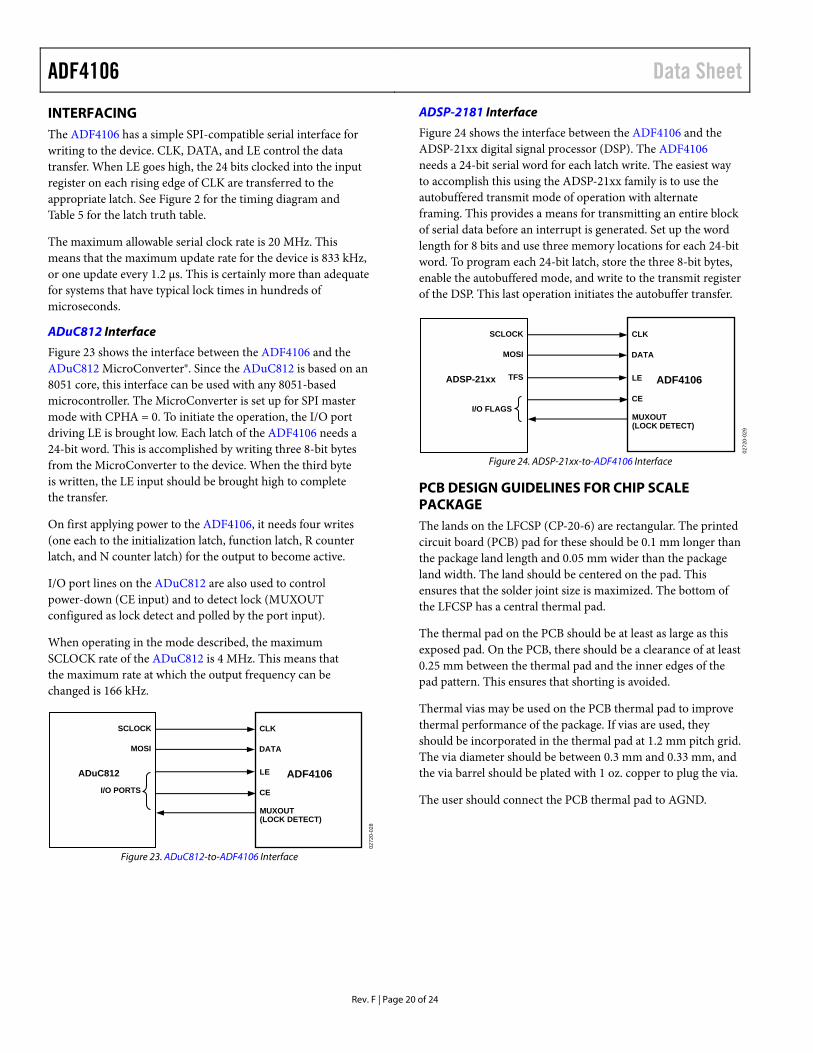
ADSP-2181 Interface
Figure 24 shows the interface between the ADF4106 and the ADSP-21xx digital signal processor (DSP). The ADF4106 needs a 24-bit serial word for each latch write. The easiest way to accomplish this using the ADSP-21xx family is to use the autobuffered transmit mode of operation with alternate framing. This provides a means for transmitting an entire block of serial data before an interrupt is generated. Set up the word length for 8 bits and use three memory locations for each 24-bit word. To program each 24-bit latch, store the three 8-bit bytes, enable the autobuffered mode, and write to the transmit register of the DSP. This last operation initiates the autobuffer transfer.
CLK
DATA
LE
CE
MUXOUT(LOCK DETECT)
MOSI
ADF4106
SCLOCK
I/O FLAGS
ADSP-21xx TFS
0272
0-02
9
Figure 24. ADSP-21xx-to-ADF4106 Interface
PCB DESIGN GUIDELINES FOR CHIP SCALE PACKAGE The lands on the LFCSP (CP-20-6) are rectangular. The printed circuit board (PCB) pad for these should be 0.1 mm longer than the package land length and 0.05 mm wider than the package land width. The land should be centered on the pad. This ensures that the solder joint size is maximized. The bottom of the LFCSP has a central thermal pad.
The thermal pad on the PCB should be at least as large as this exposed pad. On the PCB, there should be a clearance of at least 0.25 mm between the thermal pad and the inner edges of the pad pattern. This ensures that shorting is avoided.
Thermal vias may be used on the PCB thermal pad to improve thermal performance of the package. If vias are used, they should be incorporated in the thermal pad at 1.2 mm pitch grid. The via diameter should be between 0.3 mm and 0.33 mm, and the via barrel should be plated with 1 oz. copper to plug the via.
The user should connect the PCB thermal pad to AGND.
Rev. F | Page 20 of 24

Data Sheet ADF4106
Rev. F | Page 21 of 24
OUTLINE DIMENSIONS
16 9
81
PIN 1
SEATINGPLANE
8°0°
4.504.404.30
6.40BSC
5.105.004.90
0.65BSC
0.150.05
1.20MAX
0.200.09 0.75
0.600.45
0.300.19
COPLANARITY0.10
COMPLIANT TO JEDEC STANDARDS MO-153-AB Figure 25. 16-Lead Thin Shrink Small Outline Package [TSSOP]
(RU-16) Dimensions shown in millimeters
0.50BSC
0.650.600.55
0.300.250.18
COMPLIANT TO JEDEC STANDARDS MO-220-WGGD-1.
BOTTOM VIEWTOP VIEW
EXPOSEDPAD
PIN 1INDICATOR
4.104.00 SQ3.90
SEATINGPLANE
0.800.750.70 0.05 MAX
0.02 NOM
0.20 REF
0.20 MIN
COPLANARITY0.08
PIN 1INDICATOR
2.302.10 SQ2.00
FOR PROPER CONNECTION OFTHE EXPOSED PAD, REFER TOTHE PIN CONFIGURATION ANDFUNCTION DESCRIPTIONSSECTION OF THIS DATA SHEET.
120
61011
1516
5
08-1
6-20
10-B
Figure 26. 20-Lead Lead Frame Chip Scale Package [LFCSP_WQ]
4 mm × 4 mm Body, Very Very Thin Quad (CP-20-6)
Dimensions shown in millimeters

ADF4106 Data Sheet
ORDERING GUIDE Model1 Temperature Range Package Description Package Option ADF4106BRU –40°C to + 85°C 16-Lead Thin Shrink Small Outline Package (TSSOP) RU-16 ADF4106BRU-REEL –40°C to + 85°C 16-Lead Thin Shrink Small Outline Package (TSSOP) RU-16 ADF4106BRU-REEL7 –40°C to + 85°C 16-Lead Thin Shrink Small Outline Package (TSSOP) RU-16 ADF4106BRUZ –40°C to + 85°C 16-Lead Thin Shrink Small Outline Package (TSSOP) RU-16 ADF4106BRUZ-RL –40°C to + 85°C 16-Lead Thin Shrink Small Outline Package (TSSOP) RU-16 ADF4106BRUZ-R7 –40°C to + 85°C 16-Lead Thin Shrink Small Outline Package (TSSOP) RU-16 ADF4106BCPZ –40°C to + 85°C 20-Lead Lead Frame Chip Scale Package (LFCSP_WQ) CP-20-6 ADF4106BCPZ-RL –40°C to + 85°C 20-Lead Lead Frame Chip Scale Package (LFCSP_WQ) CP-20-6 ADF4106BCPZ-R7 –40°C to + 85°C 20-Lead Lead Frame Chip Scale Package (LFCSP_WQ) CP-20-6 EV-ADF4106SD1Z Evaluation Board EV-ADF411XSD1Z Evaluation Board
1 Z = RoHS Compliant.
Rev. F | Page 22 of 24

Data Sheet ADF4106
NOTES
Rev. F | Page 23 of 24

ADF4106 Data Sheet
NOTES
©2001–2015 Analog Devices, Inc. All rights reserved. Trademarks and registered trademarks are the property of their respective owners. D02720-0-4/15(F)
Rev. F | Page 24 of 24