Embed Size (px)
Citation preview

International Journal of Science and Research (IJSR) ISSN (Online): 2319-7064
Index Copernicus Value (2013): 6.14 | Impact Factor (2014): 5.611
Volume 4 Issue 11, November 2015
www.ijsr.net Licensed Under Creative Commons Attribution CC BY
Design and Analysis of Dynamic Comparator with Reduced Power and Delay
Shashank Shekhar
1, Dr. S. R. P. Sinha
2
1Research Scholar, Electronics Engineering Department, Institute of Engineering and Technology, Lucknow, India
2Associate Professor, Electronics Engineering Department, Institute of Engineering and Technology, Lucknow, India
Abstract: The need for low-power and high speed analog-to-digital converters is pushing toward the use of dynamic comparators to maximize speed and power efficiency. In this paper, performances of various types of the dynamic comparators are being compared in terms of speed, delay and power. Based on the presented analysis, a new dynamic comparator is proposed, where the circuit of a conventional comparator is modified for low-power and fast operation even in small supply voltages. It is shown that in the proposed dynamic comparator both the power consumption and delay time are reduced. The circuits are simulated using TANNER tool with 0.18μm technology and supply voltage 1.8V.
Keyword: Preamplifier, Kickback noise, Dynamic Latch Comparator, Transmission Gate, Parasitic Node Capacitance. 1. Introduction
Comparators are most probably second most widely used electronic components after operational amplifiers in this modern era. Comparators are known as 1-bit analog-to-digital converter and for that reason they are mostly used in large abundance in analog to digital converter. Apart from that, comparators are also can be found in many other applications like zero-crossing detectors, peak detectors, switching power regulators, data transmission, and others. Nowadays, where demand for portable battery operated devices is increasing, a major importance is given towards low power methodologies for high speed applications. Also we have to minimize the power consumption by using smaller feature size processes. However when we move towards power consumption minimization, the process variations and other parameters will greatly affect the overall performance of the device. Dynamic comparators are used in ADCs because these comparators have high speed, less power dissipation, less static power consumption. Also back-to-back inverters are used in dynamic comparators to provide positive feedback mechanism which converts a smaller voltage difference to full scale digital level output. However, it has a larger input referred offset compared to linear amplifiers. The reason is that in addition to static 𝑉𝑡ℎ and β mismatch, it also suffers from dynamic offset due to imbalance of parasitic capacitors at internal nodes during evaluation. [1]. In this paper we have taken dynamic latch comparator using preamplifier and dynamic latch with inverter buffer, Double tail latch type voltage sense amplifier and proposed the dynamic comparator. In preamplifier based comparator an amplifier is added before a latched stager which significantly decreases the effects of the offset voltage errors caused by device mismatch [10]. Transmission gates are used between preamplifier and latch to control the signal path and to provide high gain to the output signal of the amplifier. The major disadvantages of dynamic latch are the kickback noise [2] produced by high transmission currents which induces spikes at the differential input voltage signal. Speed and
offset of latch type voltage sense amplifier is very much dependent on the common mode voltage of the input and hence it is less attractive for ADCs In buffered latch comparator inverter buffers are added to the output of the dynamic latch comparator to isolate the comparator output from large capacitive loads [3]. The proposed dynamic comparator shows less power consumption and reduced delay compared with other comparator circuits discussed in this paper. 2. Methodology
2.1 Preamplifier Based Comparator [4]
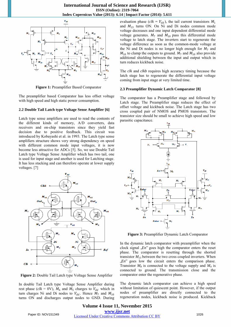
It consists of three stages: preamplifier stage, latch stage and buffer stage. The preamplifier stage is differential amplifier with active load. It amplifies a small input voltage (Vp and Vn) to improve the comparator sensitivity and isolates the input of the comparator from switching noise (often called kickback noise) coming from the positive feedback stage [2]. The positive feedback latch stage is used to determine which of the input signals (i+ or i-) is larger which is received from preamplifier stage of the comparator and extremely amplifies their difference. The difference is applied to the output buffer stage.
The output buffer stage is basically a self biased differential amplifier followed by an inverter which gives the digital output (logic „0‟ or logic „1‟). The output buffer should accept a differential input signal and not have slew-rate limitations. The circuit of the output buffer is basically a self-biased differential amplifier followed by an inverter. The inverter is added as a separate additional gain stage and isolates any load capacitance from differential amplifier.
Paper ID: NOV151349 1025
International Journal of Science and Research (IJSR) ISSN (Online): 2319-7064
Index Copernicus Value (2013): 6.14 | Impact Factor (2014): 5.611
Volume 4 Issue 11, November 2015
www.ijsr.net Licensed Under Creative Commons Attribution CC BY
Figure 1: Preamplifier Based Comparator
The preamplifier based Comparator has less offset voltage with high speed and high static power consumption.
2.2 Double Tail Latch type Voltage Sense Amplifier [6]
Latch type sense amplifiers are used to read the contents of the different kinds of memory, A/D converters, data receivers and on-chip transistors since they yield fast decision due to positive feedback. This circuit was introduced by Kobayashi et al. in 1993. The Latch type sense amplifiers structure shows very strong dependency on speed with different common mode input voltages, it is now become less attractive for ADCs [5]. So, we use Double Tail Latch type Voltage Sense Amplifier which has two tail, one is used for input stage and another is used for Latching stage. It has less stacking and can therefore operate at lower supply voltages. [7]
Figure 2: Double Tail Latch type Voltage Sense Amplifier
In double Tail Latch type Voltage Sense Amplifier during rest phase (clk = 0V), 𝑀6 and 𝑀5 charges to 𝑉𝑑𝑑 which in turn charges Ni and Di nodes to 𝑉𝑑𝑑 . Hence 𝑀7 and 𝑀10 turns ON and discharges output nodes to GND. During
evaluation phase (clk = 𝑉𝑑𝑑 ), the tail current transistors 𝑀1 and 𝑀13 turns ON. On Ni and Di nodes common mode voltage decreases and one input dependent differential mode voltage generates. 𝑀7 and 𝑀10 pass this differential mode voltage to latch stage. The inverters start to regenerate the voltage difference as soon as the common-mode voltage at the Ni and Di nodes is no longer high enough for 𝑀7 and 𝑀10 to clamp the outputs to ground. 𝑀7 and 𝑀10 also provide additional shielding between the input and output which in turn reduces kickback noise.
The clk and clkb requires high accuracy timing because the latch stage has to regenerate the differential input voltage coming from input stage at very limited time.
2.3 Preamplifier Dynamic Latch Comparator [8]
The comparator has a Preamplifier stage and followed by Latch stage. The Preamplifier stage reduces the effect of offset voltage and kickback noise. The Latch stage has two cross coupled pair of NMOS and PMOS transistors. The transistor size should be small to achieve high speed and low parasitic capacitance.
Figure 3: Preamplifier Dynamic Latch Comparator
In the dynamic latch comparator with preamplifier when the clock signal „En‟ goes high the comparator enters the reset phase. The comparator is resetting through the shorted transistor M13 between the two cross coupled inverters. When „En‟ goes low the circuit enters the comparison phase. Transistor M8 is connected to the voltage supply and M4 is connected to ground. The transmission close and the comparator enter the regenerative phase.
The dynamic latch comparator can achieve a high speed without limitation of quiescent point. However, if the output nodes of preamplifier are directly connected to the regeneration nodes, kickback noise is produced. Kickback
Paper ID: NOV151349 1026

International Journal of Science and Research (IJSR) ISSN (Online): 2319-7064
Index Copernicus Value (2013): 6.14 | Impact Factor (2014): 5.611
Volume 4 Issue 11, November 2015
www.ijsr.net Licensed Under Creative Commons Attribution CC BY
noise is produced due to high transmission currents resulting in voltage spikes at the voltage differential input signal. Hence, transmission gates are used to control the signal path between preamplifier and latch. 2.4 Dynamic Latch Comparator with Inverter Buffer [9]
The schematic of the dynamic latch comparator with inverter buffer is shown in figure 4. The transistors 𝑀1, 𝑀9 and 𝑀2, 𝑀7 form the pair of inverters and their outputs are connected to the inputs of the other. When the latch signal (Lth) is low and the transistors 𝑀5 and 𝑀8 are OFF and 𝑀1, 𝑀2 are separated from 𝑀9 and 𝑀7 and the output node is pre charged to digital logic "1" by the transistors 𝑀3 and 𝑀4 when the latch signal (Lth) is high. The transistors 𝑀5 and 𝑀8 are ON and the drain voltages of 𝑀1 and 𝑀2 start dropping from the positive rail. If the input is larger than the reference, the voltage at drain of 𝑀1 will drop faster than the output node. When the input reaches 𝑉𝑑𝑑 − 𝑉𝑡ℎ , 𝑀2 starts turning on and triggers the regenerative feedback.
Figure 4: Dynamic Latch Comparator with Inverter Buffer
In Dynamic Comparator inverter buffer are added to isolate the comparator output and the large load capacitance. The function of the switches used between the pair of inverters of buffers is to connect and disconnect the buffer output. The inverter buffers are used to minimize the offset errors.
The major drawback of the dynamic latch comparator with inverter buffer is the offset error caused by transistor mismatch and unbalanced charge residues [10].
2.5 Proposed Dynamic Comparator
The schematic of the proposed dynamic comparator is shown in figure 5. When Clk = „0‟ then transistor M1 is OFF and transistor M5 and M4 are ON and this charges nodes fn and fp to Vdd. The charged nodes fn and fp turn ON transistors M8 and M9 which discharge output nodes Outp and Outn to zero. As, Clk goes low then Clkb goes high so transistor M10 is OFF and latch is disconnected from Vdd and easily gets discharged.
When Clk = „1‟ then transistor M1 turns ON and nodes fp and fn start discharging at different rates. Once any of these nodes goes below Vdd it forces the other node to Vdd through transistors M6 and M7. The potential of these nodes drive the transistors M8 and M9. As potential of fp and fn starts decreasing due to discharging these transistors (M8, M9) and start turning OFF. Among M8 and M9 whichever turns OFF first the node corresponding to that transistor will go high as M10 and PMOS devices of latch are already ON.
Figure 5: Proposed Dynamic Latch Comparator
Proposed Dynamic Comparator derived from the fact that the comparator uses one tail for input stage and another for latching stage. It has less stacking and can therefore operate at lower supply voltages. Large size of the transistor 𝑀10 enables large current at latching stage which is independent of common mode voltages at inputs and small size of 𝑀1 offers lower supply voltages resulting lower offset.
3. Simulation Results Table 1 shows the comparison of power, delay, speed and Power Delay Product (PDP) of various comparators and Proposed Dynamic Comparator. The circuits are simulated using the TANNER EDA tool with 180nm technology. The Input specifications of simulated circuits are as follows: supply voltage (Vdd) is 1.8V, clock rise and fall time 100ns, clock delay is 1ns and clock frequency is 250 MHz. Figure 6,7,8,9 and 10 are transient analysis of Preamplifier based Comparator, Double Tail Latch Type Voltage Sense Amplifier, Preamplifier Dynamic Latch Comparator, Dynamic Latch Comparator with Inverter Buffer and Proposed Dynamic Comparator respectively.
Paper ID: NOV151349 1027

International Journal of Science and Research (IJSR) ISSN (Online): 2319-7064
Index Copernicus Value (2013): 6.14 | Impact Factor (2014): 5.611
Volume 4 Issue 11, November 2015
www.ijsr.net Licensed Under Creative Commons Attribution CC BY
Table 1: Comparison of various Comparators with Proposed Dynamic Comparator
Comparator Power
(mW)
Delay
(ps)
Speed
(GHz)
PDP
(1014)
Preamplifier based Comparator 0.397 50.10 2.1 1.98 Double Tail Latch Type Voltage
Sense Amplifier
0.225 71.12 1.4 1.56
Preamplifier Dynamic Latch
Comparator
0.221 76.56 1.31 1.69
Dynamic Latch Comparator
with Inverter Buffer
0.256 75.66 1.32 1.94
Proposed Dynamic Comparator 0.191 69.11 1.44 1.31
In Transient analysis of Preamplifier based Comparator plot is drawn for Input Signal (Vp), Reference Signal (Vn), Output Signal (Vout) with respect to time.
Figure 6: Transient analysis of Preamplifier based
Comparator In Transient analysis Double Tail Latch Type Voltage Sense Amplifier plot is drawn for Input Signal (In), Reference Signal (ref), Output Signal (Outp and Outn), Clock, with respect to time.
Figure 7: Transient analysis Double Tail Latch Type
Voltage Sense Amplifier
In Transient analysis Preamplifier Dynamic Latch Comparator plot is drawn for Input Signal (Vn+), Reference
Signal (Vn-), Output Signal (Vout+ and Vout-), Enable, with respect to time.
Figure 8: Transient analysis Preamplifier Dynamic
Latch Comparator In Transient analysis of Dynamic Latch Comparator with Inverter Buffer plot is drawn for Input Signal (Vp), Reference Signal (Vref), Output Signal (Vout+ and Vout-), Latch, with respect to time.
Figure 9: Transient analysis of Dynamic Latch Comparator
with Inverter Buffer In Transient analysis of Proposed Dynamic Comparator plot is drawn for Input Voltage (Inn), Reference Voltage (Inp), Output Voltage (Outp and Outn), Clock, with respect to time.
Paper ID: NOV151349 1028

International Journal of Science and Research (IJSR) ISSN (Online): 2319-7064
Index Copernicus Value (2013): 6.14 | Impact Factor (2014): 5.611
Volume 4 Issue 11, November 2015
www.ijsr.net Licensed Under Creative Commons Attribution CC BY
Figure 10: Transient analysis of Proposed Dynamic
Comparator
4. Conclusion In this paper a comparison is made between the simulation results of the various comparators with the simulated result of proposed dynamic comparator. The comparison result shows that proposed comparator has less power consumption and power delay product as compared to present comparators with better speed. So the proposed comparator can be used in high speed ADCs, peak detectors, zero level crossing detectors and etc with reduced power consumption and high speed.
References
[1] Jun He, Sanyi Zhan, Degang Chen, and R.L. Geiger,
“Analyses of Static and Dynamic Random Offset Voltages in Dynamic Comparators,” IEEE Trans. Circuits Syst. I: Reg. Papers, vol. 56, pp. 911-919, May 2009.
[2] P.M. Figueiredo, J.C. Vital, “Kickback noise reduction techniques for CMOS latched comparators”, IEEE Trans. Circuits Syst. II 53(7), pp. 541–545, 2006.
[3] Riyan Wang Kaihang Li Jianqin Zhang Bin Nie "A High Speed High Resolution Latch Comparator for Pipeline Analog-to-Digital Converters, "IEEE International workshop, pp.28-31, April 2007.
[4] Meena Panchore, R.S. Gamad, “Low Power High Speed CMOS Comparator Design Using 0.18μm Technology”, International Journal of Electronic Engineering Research, Vol.2, No.1, pp.71-77, 2010.
[5] B. Wicht, T. Nirschl, and D. Schmitt-Landsiedel, “Yield and speed optimization of a latch-type voltage sense amplifier”, IEEE J. Solid-State Circuits, Vol. 39, pp. 1148-1158, July 2004.
[6] D. Schinkel, E. Mensink, E. Kiumperink, E. van Tuijl and B. Nauta, “A Latch-Type Voltage Sense Amplifier with 18ps Setup+Hold Time”, ISSCC Dig. Tech. Papers, pp. 314-315 and 605, Feb. 2007.
[7] H.J. Jeon, Y.B. Kim, “A Low-offset High-speed Double-tail Dual-rail Dynamic Latched Comparator”, ACM GLSVLSI‟10(Great Lakes Symposium on VLSI), May 16-18, 2010.
[8] Carlos J Solis, Gladys O. Ducoudray, "High Resolution Low power 0.6J.lm CMOS 40MHz Dynamic Latch Comparator," 53rd IEEE International Department of Electrical and Computer Engineering, Aug. 2010.
[9] Zhaohui Huang, Peixin Zhong , "An adaptive analog-to-digital converter based on low-power dynamic latch comparator," IEEE International conference, pp. 6, May 2005.
[10] Philip E. Allen and Douglas R. Holberg, CMOS Analog Circuit Design, 2nd ed., Oxford Indian Edition, 2006.
Author Profile
Dr. S.R.P. Sinha received B.Tech degree from Ranchi University in 1981 and Received M.Tech degree from University of Roorkee in 1984. In 2004, he received Ph.D degree from Lucknow University. He has teaching experience of more than 25 years. Currently, he is Associate Professor in Department of Electronics Engineering, Institute of Engineering and Technology, Lucknow. His research interests include Electronic Devices, Micro-Electronics and Low Power VLSI Design. Shashank Shekhar received B.Tech degree from Shri Ramswaroop Memorial College of Engineering and Management, Lucknow in 2011 and presently pursuing M.Tech degree from Institute of Engineering and Technology, Lucknow. His research activities are related to Low Power VLSI Design.
Paper ID: NOV151349 1029