Embed Size (px)
Citation preview

Copyright
by
Minsik Cho
2008

The Dissertation Committee for Minsik Chocertifies that this is the approved version of the following dissertation:
Physical Synthesis for Nanometer VLSI and Emerging
Technologies
Committee:
David Z. Pan, Supervisor
Tony Ambler
Jacob A. Abraham
Nur Touba
David Morton
Physical Synthesis for Nanometer VLSI and Emerging
Technologies
by
Minsik Cho, M.S.
DISSERTATION
Presented to the Faculty of the Graduate School of
The University of Texas at Austin
in Partial Fulfillment
of the Requirements
for the Degree of
DOCTOR OF PHILOSOPHY
THE UNIVERSITY OF TEXAS AT AUSTIN
August 2008

Dedicated to my family and my wife Sora

Acknowledgments
I have been undoubtedly fortunate to have Prof. David Z. Pan as my
Ph.D. advisor during my graduate study. I am deeply grateful to him. His
warm advice, continuous support, and deep insight have helped me enjoy and
balance research and life during this long journey. He has been a mentor to
work on challenging research problems together, a friend to rely on during
difficult and hard periods, and a supporter for my success in every single
moment of my past four years. I am confident that the four years with him
would shed bright light on my future career.
I wish to express gratitude to members of my Ph.D. committee for their
time out of busy schedule and many helpful comments. They are Prof. Tony
Ambler, Prof. Jacob A. Abraham, Prof. Nur Touba, and Prof. David Morton
(ME Department).
My deep gratitude and appreciation also go to many people outside UT-
Austin for their help and advice on many issues, from technical discussions to
career planning. They are Prof. Jason Cong, Prof. Martin Wong, Prof. Jiang
Hu, Prof. Patrick Madden, Prof. Sung-kyu Lim, and Dr. Gijoon Nam.
My first internship at Intel (Austin, TX) provided me excellent op-
portunities to learn about real industrial problems. I would like to thank
Mr. Madu Gumma, Dr. Anand Ramachandran, Mr. Chih-Liang Huang, Mr.
v

Jeffrey Marcks, and many others.
My two internships at IBM T. J. Watson Research Center (Yorktown
Heights, NY) were valuable experience during my graduate study. Through
these opportunities, I was able to get exposure to cutting-edge technologies in
various engineering area (including VLSI/CAD) and attack research challenges
from the industrial context in novel yet practical fashions, in tight collabora-
tion with world-class experts in VLSI/CAD including Dr. David Kung, Dr.
Ruchir Puri, Dr. Jagan Narasimhan, Dr. Hua Xiang, Dr. James Ma, Dr.
Xiaoping Tang, Dr. Haifeng Qian, Dr. Jinjun Xiong, and many more.
Last four years at UT-Austin were wonderful with all great friends from
UTDA Lab and other groups. To name a few, Tao Luo, Haoxing Ren, Anand
Ramalingam, Suhail Ahmed, Anand Rajaram, Peng Yu, Sean Shi, Joydeep
Mitra, Kun Yuan, Katrina Lu, James Ban, Ashutosh Chakraborty, Wooyoung
Jang, Jae-seok Yang, Kiwoon Kim, Duo Ding, Donnie Chen, Shanhu Shen,
Anurag Kumar, Hongjoong Shin, Jinkyu Lee, Jisun Park, Junsung Park, and
Jungsung Yang for their help and friendship. Especially, I thank Kun Yuan
and Katrina Lu for their help in various routing research and wish all the best
to their study in UT-Austin. Also, I would like to thank Melissa Campos and
Debi Prather for many administrative supports.
I dedicate my dissertation to my family back in Korea, my daughter
Marie (born during my Ph.D. program), and my lovely wife Sora. Especially,
without my wife’s love, encouragement, sacrifice, and support, this dissertation
would not have been possible. They all have been the constant source of
vi
inspiration and impetus for me to prevail throughout last four years at UT-
Austin.
Portions of this work were supported by: SRC projects, NSF Career
Award, supports from IBM, Fujitsu, Sun, Qualcomm, Intel, KLA-Tencor, IBM
Ph.D. Scholarship, and Korean Information and Communication Technology
Scholarship.
vii
Physical Synthesis for Nanometer VLSI and Emerging
Technologies
Publication No.
Minsik Cho, Ph.D.
The University of Texas at Austin, 2008
Supervisor: David Z. Pan
The unabated silicon technology scaling makes design and manufac-
turing increasingly harder in nanometer VLSI. Emerging technologies on the
horizon require strong design automation to handle the large complexity of fu-
ture systems. This dissertation studies eight related research topics in design
and manufacturing closure in nanometer VLSI as well as design optimization
for emerging technologies from physical synthesis perspective.
In physical synthesis for design closure, we study three research topics,
which are key challenges in nanometer VLSI designs: (a) We propose a highly
efficient floorplanning algorithm to minimize substrate noise for mixed-signal
system-on-a-chip designs. (b) We propose a clock tree synthesis algorithm to
reduce clock skew under thermal variation. (c) We develop a global router,
BoxRouter to enhance routability which is one of the classic but still critical
challenges in modern VLSI.
viii

In physical synthesis for manufacturing closure, we propose the first
systematic manufacturability aware routing framework to address three key
manufacturing challenges: (a) We develop a predictive chemical-mechanical
polishing model to guide global routing in order to reduce surface topogra-
phy variation. (b) We formulate a random defect minimize problem in track
routing, and develop a highly efficient algorithm. (b) We propose a lithogra-
phy enhancement technique during detailed routing based on statistical and
macro-level Post-OPC printability prediction.
Regarding design optimization of emerging technologies, we focus on
two topics, one in double patterning technology for future VLSI fabrication
and the other in microfluidics for biochips: (a) We claim double patterning
should be considered during physical synthesis, and propose an effective double
patterning technology aware detailed routing algorithm. (b) We propose a
droplet routing algorithm to improve routability in digital microfluidic biochip
design.
ix

Table of Contents
Acknowledgments v
Abstract viii
List of Tables xv
List of Figures xvii
Chapter 1. Introduction 1
1.1 Challenges and Directions for Physical Synthesis . . . . . . . . 1
1.2 Overview and Contributions of This Dissertation . . . . . . . . 3
Chapter 2. Physical Synthesis for Design Closure 6
2.1 Substrate Noise Minimization during Floorplanning . . . . . . 9
2.1.1 Substrate Noise Model . . . . . . . . . . . . . . . . . . . 12
2.1.2 Block Preference Directed Graph . . . . . . . . . . . . . 15
2.1.2.1 Substrate Noise Table Construction . . . . . . . 17
2.1.2.2 Analog Block Ordering . . . . . . . . . . . . . . 17
2.1.2.3 Digital Block Ordering . . . . . . . . . . . . . . 18
2.1.2.4 BPDG Construction . . . . . . . . . . . . . . . 18
2.1.3 Substrate Noise Estimation with BPDG . . . . . . . . . 20
2.1.3.1 Sequence-Pair and B*-Tree . . . . . . . . . . . . 22
2.1.3.2 Sequence-Pair with BPDG . . . . . . . . . . . . 22
2.1.3.3 B*-Tree with BPDG . . . . . . . . . . . . . . . 27
2.1.3.4 Fidelity and Time Complexity . . . . . . . . . . 32
2.1.4 Fast Substrate Noise-Aware Floorplanning . . . . . . . . 33
2.1.4.1 Analog Block Floorplanning . . . . . . . . . . . 34
2.1.4.2 Noise-Aware Block Inflation . . . . . . . . . . . 34
2.1.4.3 Digital Block Floorplanning . . . . . . . . . . . 35
x

2.1.5 Experimental Results . . . . . . . . . . . . . . . . . . . 35
2.2 Temperature Aware Clock Tree Synthesis . . . . . . . . . . . . 39
2.2.1 Preliminaries . . . . . . . . . . . . . . . . . . . . . . . . 42
2.2.1.1 Delay Model . . . . . . . . . . . . . . . . . . . . 42
2.2.1.2 Definitions . . . . . . . . . . . . . . . . . . . . . 42
2.2.2 Motivation and Problem Definition . . . . . . . . . . . . 44
2.2.3 TACO Algorithm . . . . . . . . . . . . . . . . . . . . . 46
2.2.3.1 Merging Diamond Construction . . . . . . . . . 50
2.2.3.2 Parent Merging Diamond Construction . . . . . 53
2.2.3.3 Final Selection and Evaluation . . . . . . . . . 55
2.2.3.4 Overall Algorithm Analysis . . . . . . . . . . . 55
2.2.4 Experimental Results . . . . . . . . . . . . . . . . . . . 55
2.3 Routability-driven Global Routing . . . . . . . . . . . . . . . . 59
2.3.1 Preliminaries . . . . . . . . . . . . . . . . . . . . . . . . 64
2.3.1.1 Global Routing Model . . . . . . . . . . . . . . 64
2.3.1.2 Global Routing Metrics . . . . . . . . . . . . . 64
2.3.2 Practical Integer Linear Programming for Global Routing 66
2.3.2.1 T-ILP . . . . . . . . . . . . . . . . . . . . . . . 67
2.3.2.2 N-ILP . . . . . . . . . . . . . . . . . . . . . . . 70
2.3.2.3 T-ILP vs. N-ILP . . . . . . . . . . . . . . . . . 72
2.3.3 BoxRouter . . . . . . . . . . . . . . . . . . . . . . . . . 74
2.3.3.1 Steiner Tree and Net Decomposition . . . . . . 78
2.3.3.2 PreRouting and Initial Box . . . . . . . . . . . 79
2.3.3.3 BoxRouting . . . . . . . . . . . . . . . . . . . . 80
2.3.3.4 PostRouting with Negotiation . . . . . . . . . . 90
2.3.4 Layer Assignment . . . . . . . . . . . . . . . . . . . . . 93
2.3.4.1 Via aware Layer Assignment . . . . . . . . . . . 95
2.3.4.2 Via/Blockage aware Layer Assignment . . . . . 97
2.3.4.3 Progressive ILP for Via/Blockage aware LayerAssignment . . . . . . . . . . . . . . . . . . . . 99
2.3.5 Experimental Results . . . . . . . . . . . . . . . . . . . 100
2.3.5.1 ISPD07 Benchmarks . . . . . . . . . . . . . . . 102
xi

2.3.5.2 ISPD98 Benchmarks . . . . . . . . . . . . . . . 103
2.3.5.3 New ISPD98 Benchmarks . . . . . . . . . . . . 105
2.4 Summary . . . . . . . . . . . . . . . . . . . . . . . . . . . . . . 108
Chapter 3. Physical Synthesis for Manufacturing Closure 110
3.1 Manufacturability Aware Routing Framework . . . . . . . . . . 115
3.2 Global Routing for CMP and Timing optimization . . . . . . . 116
3.2.1 Predictive CMP Model and Timing Impact . . . . . . . 119
3.2.1.1 Wire Density and Predictive CMP Model . . . 119
3.2.1.2 Wire Density and Timing . . . . . . . . . . . . 121
3.2.1.3 Wire Density and Congestion . . . . . . . . . . 123
3.2.2 Wire Density Driven Global Routing for CMP and Timing125
3.2.2.1 Minimum Pin Density Routing . . . . . . . . . 125
3.2.2.2 Timing Sensitivity Map Construction . . . . . . 126
3.2.2.3 CMP Aware Wire Density Distribution . . . . . 129
3.2.2.4 Wire Density Driven Maze Routing . . . . . . . 130
3.2.3 Experimental Results . . . . . . . . . . . . . . . . . . . 131
3.3 Track Routing for Random Defect Optimization . . . . . . . . 134
3.3.1 Preliminaries . . . . . . . . . . . . . . . . . . . . . . . . 138
3.3.1.1 Track Routing . . . . . . . . . . . . . . . . . . . 138
3.3.1.2 Notations . . . . . . . . . . . . . . . . . . . . . 141
3.3.1.3 Critical Area and Probability of Failure . . . . . 142
3.3.1.4 Second Order Cone Programming . . . . . . . . 143
3.3.2 TROY Algorithm . . . . . . . . . . . . . . . . . . . . . 145
3.3.2.1 Yield-driven track routing . . . . . . . . . . . . 145
3.3.2.2 Wire Ordering Optimization . . . . . . . . . . . 151
3.3.2.3 Globally Optimal Wire Sizing and Spacing . . . 155
3.3.2.4 Runtime Complexity Analysis . . . . . . . . . . 159
3.3.3 Experimental Results . . . . . . . . . . . . . . . . . . . 160
3.4 Detailed Routing for Lithography Enhancement . . . . . . . . 166
3.4.1 Previous Works . . . . . . . . . . . . . . . . . . . . . . . 169
3.4.2 Pre-OPC and Post-OPC EPE Comparison . . . . . . . . 173
xii

3.4.3 Post-OPC Printability Prediction . . . . . . . . . . . . . 176
3.4.3.1 Statistical WGT Characterization . . . . . . . . 176
3.4.3.2 Compact Litho-Metric with OPC . . . . . . . . 180
3.4.3.3 High Fidelity of Our Litho-Metric . . . . . . . . 183
3.4.4 ELIAD Algorithm . . . . . . . . . . . . . . . . . . . . . 185
3.4.5 Experimental Results . . . . . . . . . . . . . . . . . . . 189
3.5 Summary . . . . . . . . . . . . . . . . . . . . . . . . . . . . . . 195
Chapter 4. Physical Synthesis for Emerging Technologies 197
4.1 Double Patterning Technology . . . . . . . . . . . . . . . . . . 199
4.1.1 Background and Definitions . . . . . . . . . . . . . . . . 202
4.1.1.1 Double Patterning Technology (DPT) . . . . . 203
4.1.1.2 Challenges in DPT . . . . . . . . . . . . . . . . 205
4.1.1.3 Definitions . . . . . . . . . . . . . . . . . . . . . 206
4.1.1.4 Complexity of Layout Decomposition . . . . . . 208
4.1.2 DPT-Friendly Detailed Routing . . . . . . . . . . . . . . 211
4.1.2.1 DPT Consideration during Design . . . . . . . . 211
4.1.2.2 Routing Path Coloring . . . . . . . . . . . . . . 214
4.1.2.3 Detailed Routing Algorithm . . . . . . . . . . . 218
4.1.3 Experimental Results . . . . . . . . . . . . . . . . . . . 220
4.2 Digital Microfluidic Biochips . . . . . . . . . . . . . . . . . . . 223
4.2.1 Background and Problem Formulation . . . . . . . . . . 227
4.2.1.1 Digital Microfluidic Biochip . . . . . . . . . . . 227
4.2.1.2 Routing for Digital Microfluidic Biochip . . . . 230
4.2.2 High-Performance Droplet Routing Algorithm . . . . . . 236
4.2.2.1 Routing by Bypassibility . . . . . . . . . . . . . 238
4.2.2.2 Routing with Concession . . . . . . . . . . . . . 244
4.2.2.3 Solution Compaction . . . . . . . . . . . . . . . 246
4.2.2.4 Three-droplet Routing Handling . . . . . . . . . 248
4.2.2.5 Runtime Complexity Analysis . . . . . . . . . . 248
4.2.3 Experimental Results . . . . . . . . . . . . . . . . . . . 249
4.2.3.1 Results on Benchmark Suite I . . . . . . . . . . 249
4.2.3.2 Results on Benchmark Suite II . . . . . . . . . 251
4.3 Summary and Future Directions . . . . . . . . . . . . . . . . . 255
xiii

Chapter 5. Conclusion 257
Bibliography 260
Index 296
Vita 297
xiv

List of Tables
2.1 Substrate noise table. . . . . . . . . . . . . . . . . . . . . . . . 16
2.2 Experimental results with Sequence-Pair (-sp) and B*-Tree (-bt). 36
2.3 The notations in this section. . . . . . . . . . . . . . . . . . . 43
2.4 Experimental results for the initial clock tree from BST [96]. . 56
2.5 Experimental result for the optimized clock tree from TACO. . 56
2.6 The notations in this section. . . . . . . . . . . . . . . . . . . 64
2.7 ISPD07 IBM benchmarks [103]. . . . . . . . . . . . . . . . . . 100
2.8 Comparison between ISPD07 contestants (including all win-ners) and ours on ISPD07 benchmarks. . . . . . . . . . . . . . 101
2.9 ISPD98 IBM benchmarks [101]. . . . . . . . . . . . . . . . . . 103
2.10 Comparison between published global routers and ours on ISPD98benchmarks. . . . . . . . . . . . . . . . . . . . . . . . . . . . . 104
2.11 BoxRouter results on ISPD98H/I benchmarks. . . . . . . . . . 106
3.1 Comparison with BoxRouter for ISPD98 benchmarks. . . . . . 133
3.2 The notations in this section. . . . . . . . . . . . . . . . . . . 140
3.3 ISPD98 IBM benchmarks. . . . . . . . . . . . . . . . . . . . . 161
3.4 Comparison between greedy track router and TROY (α = 0.6). 163
3.5 Pre-OPC EPE and Post-OPC EPE mapping based on 544Ksampling point shows that they are highly uncorrelated (R=-0.36). . . . . . . . . . . . . . . . . . . . . . . . . . . . . . . . . 190
3.6 Comparison between various routers on two industrial designs. 192
3.7 Detailed EPE reduction (%) over DR comparison between DR+RRand ELIAD by partition. . . . . . . . . . . . . . . . . . . . . . 193
4.1 Grid state for DPT coloring. . . . . . . . . . . . . . . . . . . . 214
4.2 Lookup table for DPT routing. . . . . . . . . . . . . . . . . . 218
4.3 Performance of the proposed DPT-friendly detailed routing al-gorithm. . . . . . . . . . . . . . . . . . . . . . . . . . . . . . . 222
4.4 The notations in this section. . . . . . . . . . . . . . . . . . . 232
xv

4.5 Bypassibility analysis table. . . . . . . . . . . . . . . . . . . . 239
4.6 Comparison between the prioritized A* search, the two-stagerouting algorithm, the network-flow based algorithm, and ouralgorithm on Benchmark Suite I. . . . . . . . . . . . . . . . . 250
4.7 Comparison between the prioritized A* search, the network-flowbased algorithm, and our algorithm on Benchmark Suite II. . . 253
4.8 Comparison between the prioritized A* search and our algorithm.254
4.9 Comparison between the network-flow based algorithm and ouralgorithm. . . . . . . . . . . . . . . . . . . . . . . . . . . . . . 255
xvi

List of Figures
2.1 Macromodel for the substrate based two-port lumped resistornetwork. . . . . . . . . . . . . . . . . . . . . . . . . . . . . . . 13
2.2 Two different size blocks with separation x and relative positiony. . . . . . . . . . . . . . . . . . . . . . . . . . . . . . . . . . . 14
2.3 Analog block orderings. . . . . . . . . . . . . . . . . . . . . . . 17
2.4 Digital block orderings. . . . . . . . . . . . . . . . . . . . . . . 18
2.5 The block preference directed graph (BPDG) built from Table 2.1. 20
2.6 The basic concept of substrate noise estimation with BPDG. . 21
2.7 Floorplan example where the strict below set of Ba includes B2,B3 and B4, and the reference block of Ba is B3. . . . . . . . . 23
2.8 Floorplan examples. . . . . . . . . . . . . . . . . . . . . . . . 25
2.9 Floorplan example with the corresponding B*-Tree. . . . . . . 28
2.10 Example of parent-children relationships by different block lo-cations. . . . . . . . . . . . . . . . . . . . . . . . . . . . . . . 29
2.11 Number of violations vs. substrate noise. . . . . . . . . . . . . 32
2.12 Empirical time complexity of BPDG based substrate noise es-timation. . . . . . . . . . . . . . . . . . . . . . . . . . . . . . . 33
2.13 Time for comparing BPDG against Sequence-Pair/B*-Tree. . . 38
2.14 Result of packing ami49 with Sequence-Pair. . . . . . . . . . . 39
2.15 Motivation and concept of merging diamond. . . . . . . . . . . 45
2.16 Bottom-up and top-down phases in TACO. . . . . . . . . . . . 48
2.17 (a-c) an equal delay point a/b/c is found along a given path be-tween two children, u and v; (d) an equal delay point d is foundand an equal delay merging diamond eMD(p) is constructed. 50
2.18 Equal delay point projection. . . . . . . . . . . . . . . . . . . 51
2.19 Merging diamond shrinkage. . . . . . . . . . . . . . . . . . . . 53
2.20 Balanced skew and parent merging diamond construction. . . 54
2.21 Skew variations for three kinds of clock trees of r5 by the variousthermal gradients. . . . . . . . . . . . . . . . . . . . . . . . . . 57
xvii
2.22 Initial clock tree (shown in solid line), and optimized clock tree(shown in dotted line) after TACO of r3. . . . . . . . . . . . . 58
2.23 A real circuit with netlists can be dissected into multiple gridswhich can be mapped into graph for global routing with routingcapacity on an edge. . . . . . . . . . . . . . . . . . . . . . . . 65
2.24 Example of ILP for global routing with two possible routingsolutions is shown. Two routing solutions in (c) and (d) arevalid w.r.t. the given routing capacities, but different in termsof congestion distribution. The one in (c) achieves more uniformcongestion distribution. T-ILP prefers routing (c) to routing(d), while N-ILP has no preference. . . . . . . . . . . . . . . 68
2.25 T-ILP formulation for the example of Fig. 2.24 (b). . . . . . . 69
2.26 General T-ILP formulation. . . . . . . . . . . . . . . . . . . . 69
2.27 N-ILP formulation for the example of Fig. 2.24 (b). . . . . . . 70
2.28 General N-ILP formulation. . . . . . . . . . . . . . . . . . . . 71
2.29 Runtimes of T-ILP and N-ILP are compared. It shows that N-ILP is much faster and more scalable for larger problems thanT-ILP. . . . . . . . . . . . . . . . . . . . . . . . . . . . . . . . 75
2.30 The basic concept of BoxRouter. . . . . . . . . . . . . . . . . 76
2.31 BoxRouter consists of three main steps: PreRouting, BoxRout-ing, and PostRouting. BoxRouting can be further composed ofprogressive ILP and adaptive maze routing. . . . . . . . . . . 77
2.32 Net can be decomposed into two pin wires with Rectilinear Min-imum Steiner Tree Construction. . . . . . . . . . . . . . . . . 78
2.33 Congestion estimations after PreRouting and BoxRouting arecompared. It shows that simple PreRouting can effectively cap-ture overall congestion as well as the most congested region. . 80
2.34 Progressive ILP formulation of Fig. 2.35 (c). . . . . . . . . . . 81
2.35 BoxRouting example. . . . . . . . . . . . . . . . . . . . . . . . 82
2.36 General progressive ILP formulation. . . . . . . . . . . . . . . 83
2.37 Efficient multi-source multi-target maze routing examples areillustrated. More efficient alternative paths are found by con-sidering multiple sources and targets. . . . . . . . . . . . . . . 85
2.38 Multi-source multi-target with bridge maze routing model. . . 87
2.39 Dynamically scaled A* search reduces congestions robustly andstably over iterations. . . . . . . . . . . . . . . . . . . . . . . . 91
xviii

2.40 Topology aware wire ripup improves routing flexibility by rip-ping up some connected wires, but honors the current routingtopology. . . . . . . . . . . . . . . . . . . . . . . . . . . . . . . 93
2.41 Layer assignment can determine the number of vias as shownin (b) and (c). Also, the location of blockages in 3D can affectroutability in (d). . . . . . . . . . . . . . . . . . . . . . . . . . 94
2.42 ILP formulation for via aware layer assignment. . . . . . . . . 95
2.43 Example of ILP formulation for via aware layer assignment forFig. 2.41 (a). . . . . . . . . . . . . . . . . . . . . . . . . . . . 96
2.44 ILP formulation for via/blockage aware layer assignment. . . . 98
2.45 Progressive ILP based on box expansion is efficient in manag-ing problem size tractable, while honoring the solutions fromprevious iterations. . . . . . . . . . . . . . . . . . . . . . . . . 99
2.46 Congestion map of routed adaptec5. . . . . . . . . . . . . . . . 102
2.47 Runtime exponentially depends on total routing capacity, whilewirelength shows quadratic dependency. . . . . . . . . . . . . 107
2.48 Although ibm01 in ISPD98H benchmarks has less capacity thanibm01 in ISPD98, ours achieves zero-overflowed solution bystrongly spreading out wires to less congested regions. . . . . . 108
3.1 Context dependent minimum spacing rule for 65nm technologyis shown [66]. Both cases, (a) and (b) are described in the table. 111
3.2 Manufacturability aware routing framework. . . . . . . . . . . 115
3.3 Normalized Cu thickness by metal density. . . . . . . . . . . . 120
3.4 Predictive CMP model. . . . . . . . . . . . . . . . . . . . . . . 121
3.5 Difference between congestion and density . . . . . . . . . . . 124
3.6 Example of minimum pin density routing. . . . . . . . . . . . 126
3.7 Example of timing sensitivity map construction. . . . . . . . . 127
3.8 Normalized Cu thickness distributions of four industrial designs. 129
3.9 Effectiveness of parameter P and Q. . . . . . . . . . . . . . . 132
3.10 Example of track routing is shown to illustrate the concept andits impact on design goals. For instance, track routing can resultin different wirelength, when trunk-Steiner tree is applied toestimated expected detailed wirelength. . . . . . . . . . . . . . 139
3.11 An example of track routing is shown to explain the notations. 141
3.12 The proposed yield-driven track routing formulation is shown. 147
xix

3.13 We reformulate the one in Fig. 3.12 into integer nonlinear pro-gramming (INLP) by introducing a binary variable oij whichdetermines the precedence between Wi and Wj in terms of x/ylocation in the design. . . . . . . . . . . . . . . . . . . . . . . 148
3.14 Our simplified POF oi in Eq. (3.18) fits over 99.8 % with the
data points from Eq (3.11), enabling highly efficient SOCP for-mulation. . . . . . . . . . . . . . . . . . . . . . . . . . . . . . 149
3.15 Example of two disjoint subpanels is shown. . . . . . . . . . . 151
3.16 TROY example. . . . . . . . . . . . . . . . . . . . . . . . . . . 152
3.17 Clique for wire ordering in TROY. . . . . . . . . . . . . . . . 154
3.18 After wire ordering is done, the INLP formulation in Fig. 3.13can be casted into highly efficient SOCP. . . . . . . . . . . . . 156
3.19 The empirical runtime complexity of our SOCP is O(N1.335)where N is the number of variables. Such near linear complexitymakes TROY to large scale VLSI track routing. . . . . . . . . 157
3.20 The average empirical runtime complexity of our SOCP for onelayer is O(C1.276) where C is the number of cells. . . . . . . . 159
3.21 The distribution of 10K defects for Monte-Carlo simulation isshown. . . . . . . . . . . . . . . . . . . . . . . . . . . . . . . . 162
3.22 Trade-off between open and short defects is shown by α. . . . 164
3.23 Total number of defects from all the benchmark circuits is shownby different algorithms. Each step of TROY (minimum Hamil-tonian path based wire ordering and second order cone pro-gramming based wire sizing/spacing) is superior to the counterpart in greedy approach, and TROY can achieve 18% yield lossreduction, compared with the greedy yield-driven track router. 165
3.24 Illustration of optical lithography system for VLSI manufacturing.170
3.25 Convolution lookup for fast lithography simulation [241]. . . . 172
3.26 This plot shows how a pre-OPC EPE distribution will be mappedto a post-OPC EPE distribution. From this result, we canconclude that most pre-OPC EPE hotspots will be taken careof by OPC algorithms. Therefore, a lithography aware de-tailed router should use a post-OPC EPE metric to capturereal litho-hotspots rather than to optimize trivial easy-to-fix-by-OPC hotspots with design overhead (e.g., wirelength, runtime,via, and so on). . . . . . . . . . . . . . . . . . . . . . . . . . 174
3.27 WGT characterization for t1=jog-corner and t2=line-end is shownwhere (b), (c), (d), and (e) are the cases with the same distance.Thus, the mean EPE will characterize this interaction betweent1 and t2 at this distance. . . . . . . . . . . . . . . . . . . . . 178
xx

3.28 Respectively assuming C, F, E, and J are blockage-corner, fat-wire-edge, line-end, and jog-corner, WG Shadowing examplesare shown. Each grid has a cost array which contains the costsfor jog-corner, line-end, via, and wire. . . . . . . . . . . . . . . 181
3.29 A-B-C-D are connected based on wirelength in (b), but litho-metric in (c). . . . . . . . . . . . . . . . . . . . . . . . . . . . 182
3.30 Our litho-metric shows higher fidelity to post-OPC printabilityin larger scale. . . . . . . . . . . . . . . . . . . . . . . . . . . . 184
3.31 Simple rule-based routing can be inaccurate, while not onlyproducing more hotspots but also increasing wirelength. . . . . 188
3.32 Industrial Calibre-OPC/ORC flow. . . . . . . . . . . . . . . . 189
3.33 Experimental flow with four different routing algorithms [110]. 191
4.1 In DPT, one single layer can be decomposed into two masks toeffectively increase pitch size [13]. . . . . . . . . . . . . . . . . 200
4.2 The concept of a stitch is elaborated by an example in (a), andits susceptibility to overlay error is demonstrated in (b). . . . 201
4.3 In a DPT process, one single layer is decomposed into twomasks, and it requires two exposures and two etching [178]. . 204
4.4 This example illustrates the key DPT concepts in layout de-composition and stitch. . . . . . . . . . . . . . . . . . . . . . 207
4.5 This example describes a layout decomposition and shows thatlayout decomposition with stitch for DPT is more complex thanphase-assignment which is equivalent to 2-coloring [122]. . . . 209
4.6 This example motivates DPT consideration during detailed rout-ing. Detailed routing algorithm can make effective trade-offamong layout decomposability, wirelength, the number of stitches,and the number of vias. . . . . . . . . . . . . . . . . . . . . . 213
4.7 A routing path can be efficiently colored while minimizing thenumber of stitches, and its neighboring grids are shadowed forremaining unrouted/uncolored nets. . . . . . . . . . . . . . . 216
4.8 Performance of the proposed DPT-friendly routing on test2 withdifferent parameters. . . . . . . . . . . . . . . . . . . . . . . . 221
4.9 The schematic view of digital microfluidic biochips for colori-metric assays [18]. . . . . . . . . . . . . . . . . . . . . . . . . . 229
4.10 Graph model and fluidic constraints for digital microfluidic biochipdesign. . . . . . . . . . . . . . . . . . . . . . . . . . . . . . . . 233
4.11 Each droplet is routed during different time intervals to reduceA* search complexity. . . . . . . . . . . . . . . . . . . . . . . . 235
xxi

4.12 The bypassibility is based on whether there exist bypasses forthe unrouted droplets. . . . . . . . . . . . . . . . . . . . . . . 238
4.13 This example describes the proposed droplet routing algorithm.After the first three routings, (b)-(d) are done by Algorithm 19(Routing-Bypassibility). Then, no droplet can be routed in a2D plane due to a deadlock between d1 and d2. Thus, as in Al-gorithm 18, (e) and (f) are done in a 3D plane by Algorithm 20(Routing-Concession) to resolve the deadlock. After the resolu-tion, (g) is done in 2D again by Algorithm 19, followed by thecompaction in (h) using Algorithm 21. . . . . . . . . . . . . . 242
4.14 This example shows bypassibility analysis of Fig. 4.13 (a) whered4, d2, and d3 have half (horizontal), full, and no bypassibility,respectively. . . . . . . . . . . . . . . . . . . . . . . . . . . . . 243
4.15 test16 in Table 4.7 has over 20% blockages area and 24 droplets. 251
xxii

Chapter 1
Introduction
1.1 Challenges and Directions for Physical Synthesis
In last half century, the semiconductor industry has made spectacular
advancements of VLSI technology based on aggressive technology scaling, fol-
lowing the Moore’s Law where the minimum feature size is scaled down every
three years at the rate of a factor 0.7. Such exponential technology scaling pro-
vides never-experienced chip performance in a small silicon area by integrating
a tremendous number of transistors.
Physical synthesis, the process of transforming a structural logic rep-
resentation of a VLSI system into a physical and geometrical layout repre-
sentation, plays a critical role in keeping up the Moore’s law. It has provided
automated methodologies and efficient algorithms to handle large and complex
VLSI systems while satisfying various design constraints such as performance,
power, noise, life-time, and so on. However, modern physical synthesis is facing
grand challenges in both design and manufacturing sides.
On one hand, major design objectives such as congestion, power, per-
formance, reliability, and noise are often conflicting with each other in modern
designs with multi-million gates, resulting in complex design closure. Integrat-
1

ing heterogeneous circuitries on a single die as popularly done in mixed-signal
SOCs reduces overall system reliability and performance due to substrate noise.
Non-uniform temperature distribution within a chip owing to different power
consumption of different blocks increases clock skew, reducing system perfor-
mance. Congestion becomes a more critical bottleneck in chip design due to
high device density and tight integration of many functional blocks.
On the other hand, design closure no longer guarantees historical yield
norm, requiring ever-challenging manufacturing closure. The conventional
contracts between design and fab through design rules are breaking down, due
to deep subwavelength lithography and growing process variations. Topog-
raphy variation due to chemical-mechanical polishing (CMP) greatly reduces
defocus margin, degrading printability. Random defects due to missing/extra
material become a significant contributor to manufacturing yield loss, espe-
cially in a mature process. Printability problems due to critical dimension
reduction in a lithography system will get more serious, as the semiconductor
industry has no choice but to live with the current 193nm lithography till at
least 22nm generation.
Therefore, in order to continue the Moore’s law, it is indispensable
to propose advanced physical synthesis algorithms which can address all these
challenges in an effective and efficient manner. First, we need to improve physi-
cal synthesis algorithms to capture and optimize not only traditional challenges
such as routability/congestion but also arising issues such as substrate noise
and thermal effects, in order to enhance design closure of nanometer VLSI
2

designs. Next, we should propose new physical synthesis algorithms to predict
and compensate manufacturing effects with respect to a given manufacturing
technology, in order to accomplish manufacturing closure.
It is also crucial to envision the role of physical synthesis in emerging
technologies such as new silicon fabrication techniques or nano/bio technolo-
gies. Clearly, physical synthesis will continue to serve as a technology enabler,
but it will be different from the traditional VLSI physical synthesis, as the
underlying technology may have different natures/characteristics from current
VLSI manufacturing technologies. Hence, physical synthesis has to evolve in
order to support and take advantage of emerging technologies fully.
1.2 Overview and Contributions of This Dissertation
This dissertation researches eight related topics in physical synthesis
for nanometer VLSI and emerging technologies. The first three are related to
various optimization techniques and algorithms in floorplanning, clock synthe-
sis, and global routing for enhanced design closure. Next three topics are in
manufacturing closure, with emphasis on routing algorithms to reduce topog-
raphy variation, random defects, and printability degradation. The last two
research topics study physical synthesis for emerging technologies by propos-
ing enhanced or evolved routing algorithms for double patterning technology
and digital microfluidic biochips.
The rest of this dissertation will be organized as follows. Chapter 2
presents our results on physical synthesis for design closure to address substrate
3

noise in mixed-signal system-on-a-chip (SOC) floorplanning, clock synthesis
under temperature variation, and routability enhancement in global routing.
The main contributions include:
• We propose a fast yet high fidelity substrate noise estimation algorithm
based on the novel concept of block preference directed graph (BPDG),
in order to guide floorplanning for mixed-signal SOC designs.
• We propose a post-optimization algorithm for clock tree synthesis to
minimize temperature-induce clock skew with the concept of merging
diamond.
• We develop a routability-driven global router, BoxRouter to effectively
remove congestion. BoxRouter is based on multiple novel techniques in-
cluding a new integer linear programming (ILP) formulation along with
box expansion, negotiation-based rerouting, and ILP-based layer assign-
ment for via minimization.
In Chapter 3, we propose the first manufacturability aware routing
framework to optimize topography variation after chemical-mechanical polish-
ing (CMP), yield loss due to random defects, and lithography effect on local
interconnect. The main contributions include:
• We present a simple predictive CMP model verified with industrial cases
for the first time, which can guide a global router for less topography
variation as well as better timing.
4

• We propose track routing with yield optimization, TROY, which is the
first track router with yield optimization, in order to minimize probabil-
ity of failure due to random defects in a systematic fashion.
• We develop a compact and high fidelity Post-OPC litho-metric based on
statistical characterization. Then, we propose efficient lithography aware
detailed routing, ELIAD based the litho-metric in order to to optimize
printability during detailed routing.
Chapter 4 discusses physical synthesis algorithms, especially routing
algorithms for advance technology nodes (sub 32nm) with double pattern
technology and digital microfluidic biochips. The major contributions can
be summarized as follows:
• We propose the first detailed routing algorithm with double patterning
technology taken into account, in order to improve layout decomposabil-
ity and overlay control.
• We introduce the concept of bypassibility and concession for enhanced
droplet routability in digital microfluidic biochip designs, by fully utiliz-
ing the time-multiplex resource sharing nature in digital microfluidics.
Finally, Chapter 5 concludes this dissertation with summary and future
directions.
5

Chapter 2
Physical Synthesis for Design Closure
It has been widely known that physical synthesis is a crucial step for
design closure where a design must satisfy multiple objectives at the same time
such as timing, power, noise, congestion, and so on. This leads to a huge num-
ber of papers in timing, power, crosstalk, and other optimizations including
[9, 10, 47, 185, 187, 188, 230]. However, due to recent prevailing system-on-a-
chip (SOC) design and ever-increasing power consumption, substrate noise
and thermal effect become emerging barriers to successful design closure in
nanometer VLSI systems. Meanwhile, congestion or routability still remains
one of the most fundamental but complex objectives in design closure. There-
fore, we focus on substrate noise, thermal effect, and congestion issues to
enhance design closure in nanometer physical synthesis, and will present three
research results in this chapter.
In Section 2.1, we introduce a novel substrate noise estimation tech-
nique during early mixed-signal SOC floorplanning, based on the concept of
Block Preference Directed Graph (BPDG) and the classic Sequence-Pair and
B*-Tree floorplan representations. Given a set of analog and digital blocks, the
BPDG is constructed based on their inherent noise characteristics to capture
6

their preferred relative orders for substrate noise minimization. For each floor-
plan instance generated during floorplanning evaluation, we can measure its
violation against BPDG very efficiently. We observe that by simply counting
the number of violations obtained in this manner, it correlates remarkably well
with an accurate but computation-intensive substrate noise model. Thus, our
BPDG-based model has high fidelity to guide substrate noise aware floorplan-
ning and layout optimization, which become a growing concern for mixed-
signal SOCs. Our experimental results show that the proposed approach is
over 60x faster than conventional floorplanning with even very compact sub-
strate noise models. We also obtain less area and total substrate noise than
the conventional approach. Our contribution is recognized as a Best Paper
Nomination at ASPDAC’06.
In Section 2.2, an efficient temperature aware clock optimization algo-
rithm, TACO is proposed for the first time to minimize the worst case clock
skew in the presence of on-chip thermal variation. TACO, while trying to
minimize the worst case clock skew, also attempts to minimize the clock tree
wirelength by building up merging diamonds in a bottom-up manner. As an
output, TACO provides balanced merging points and modified clock routing
paths to minimize the worst case clock skew under thermal variation. Experi-
mental results on a set of standard benchmarks show 50 - 70% skew reduction
with less than 0.6% wirelength overhead. This is the first work on thermal
impact consideration in clock synthesis, and attracts many follow-up studies
including [34,35,158,159,240].
7
In Section 2.3, we propose a new routability/congestion-driven global
router, BoxRouter, powered by the concept of box expansion, progressive in-
teger linear programming (ILP), adaptive maze routing, negotiation-based
rerouting, and ILP-based layer assignment. BoxRouter first uses a simple Pre-
Routing strategy to predict and capture the most congested region with high
fidelity, compared to the final routing. Based on progressive box expansion
initiated from the most congested region, BoxRouting is performed with pro-
gressive ILP and adaptive maze routing. Our progressive ILP is shown to be
much more efficient than traditional ILP in terms of speed and quality, and the
adaptive maze routing based on a multi-source multi-target with bridge model
is effective in minimizing the congestion and wirelength. Robust negotiation-
based rerouting further enhances the routing solution by efficiently removing
congestion. Layer assignment which is powered by progressive via/blockage
aware ILP maps a 2D global routing solution to a 3D multilayer solution. Ex-
perimental results show that BoxRouter has better routability with compara-
ble wirelength than other routers on ISPD07 benchmarks, and it can complete
(no overflow) ISPD98 benchmarks for the first time in the literature with the
shortest wirelength. BoxRouter received multiple recognitions from EDA com-
munity including a Best Paper Nomination in DAC’06, ACM/SIGDA Awards
in ISPD’07 Routing Contest, and SRC Inventor Recognition Award in 2008,
and further helped to generate the recent global routing research renaissance in
VLSI CAD community as seen by a number of follow-up papers at leading con-
ferences including [31,32,79,108,157,171,176,190]. We release the BoxRouter
8

source code in http://www.cerc.utexas.edu/utda/download/BoxRouter.htm
to promote more open research.
2.1 Substrate Noise Minimization during Floorplanning
Increasing demand for wireless and telecommunication applications is
driving tighter integration of multiple heterogeneous components (e.g., front
end RF circuit, mixed-signal circuits, and high speed DSP cores) into a single
system-on-a-chip (SOC). As such components can degrade the performance
or cause failure by interfering with each other, it has to be optimized dur-
ing layout planning [164]. A major interference is the substrate noise caused
by large amount of switching activities in high speed digital cores to ana-
log/RF components, degrading the reliability and performance of these sen-
sitive analog/mixed-signal/RF IPs [131]. Such substrate noise is becoming a
growing concern due to higher clock frequency, more accurate analog precision,
deeper technology scaling, and tighter integration of analog blocks with digital
blocks [92, 136, 170]. It is known that many effects that corrupt RF signals
such as DC offset, oscillator pulling and pushing, local oscillator leakage can
be traced to the substrate-coupled noise [131].
For the purpose of minimizing coupling through substrate noise, three
different factors can be optimized such as the amount of noise from digital
circuitry, the sensitivity of analog circuitry to noise, and the transfer of the
noise from digital circuitry to analog circuitry. The common techniques to
minimize the above three factors include guard ring and N-well trench around
9

analog circuitry, separate P/G networks for digital and analog circuitries, and
floorplanning [196]. Especially, during floorplanning stage, a key step of such
layout optimization, the sensitive analog circuits and noisy digital circuits can
be placed further apart to reduce substrate noise coupling [23]. Therefore, fast
yet accurate evaluation and optimization of substrate noise in the floorplanning
has become a crucial part of mixed-signal SOC designs, in order to avoid
expensive over-design and excessive design iterations.
Although abundant amount of works have been done in modeling and
simulation of substrate noise [67,71,82,92,131,170,173,210,211], none of them
are suitable to guide substrate noise optimization in floorplanning due to high
computational expense or limited applications. Therefore, there is not much in
the literature on substrate noise optimization in an early floorplanning stage.
Mitra et al. [155] presented a substrate aware mixed-signal macrocell place-
ment with an electrothermal-like substrate model [138]. Lin et al. [142] incor-
porated substrate noise minimization into placement based on a semi-empirical
model [71]. Kao et al. [124] presented a constraint-driven placement to address
substrate noise in mixed-signal designs. The substrate noise estimation tech-
niques in these works, however, either suffer from low accuracy or high com-
plexity. Blakiewicz et al. [22] proposed a floorplanning algorithm with a more
scalable substrate noise model, but it still requires significant computational
overhead to evaluate the substrate noise as a floorplanning cost.
In this section, we propose a novel concept of block preference directed
graph (BPDG) to overcome the modeling bottleneck for substrate noise aware
10

floorplanning. Using the proposed theorems to compare a floorplan instance
in Sequence-Pair or B*-Tree against BPDG, our BPDG-based substrate model
shows high fidelity to accurate but much more expensive substrate noise mod-
eling [170], and shows significantly less computational overhead than the ac-
curate substrate noise modeling. Thus, it can efficiently guide substrate noise
aware floorplanning for mixed-signal SOCs. The major contributions of this
section include the following:
• We introduce a novel concept of block preference directed graph (BPDG)
to represent preferred relative block locations in floorplanning. In BPDG,
all the preferences are decided to minimize substrate noise, and each
preference is specified as a directed edge in BPDG. BPDG can be eas-
ily compared against existing floorplan representations for fast substrate
noise estimation.
• We propose a fast substrate noise estimation algorithm by comparing
BPDG against Sequence-Pair. We simply count how many preferences in
BPDG are not held in Sequence-Pair with simple bitwise-OR operation.
• We propose another fast substrate noise estimation algorithm by com-
paring BPDG against B*-Tree. We simply count how many preferences
in BPDG are not held in B*-Tree with simple depth-first tree traversal.
• We show that our approach has surprisingly high fidelity to the sub-
strate noise calculated by the most recent and accurate substrate noise
model [170].
11

• We propose a fast substrate noise aware floorplanning algorithm based
on BPDG with Sequence-Pair and B*-Tree representations. Our ex-
perimental results show the proposed approach is significantly (70x with
Sequence-Pair and 30x with B*-Tree) faster than a conventional simulation-
based, substrate noise aware floorplanning.
The rest of this section is organized as follows. In Section 2.1.1, our
substrate model is described. In Section 2.1.2, the concept of block preference
directed graph is introduced. Our substrate noise estimation algorithm and the
overall floorplanning flow are described in Section 2.1.3 and 2.1.4, respectively.
Experimental results are discussed in Section 2.1.5.
2.1.1 Substrate Noise Model
Several techniques have been proposed to model and analyze substrate
noise accurately in an integrated circuit [82,211,212], but we use a more com-
pact substrate coupling model [170] based on a simple resistive macromodel to
verify the final floorplan from our fast approach. The substrate noise model
in [170] is known to be highly scalable and accurate. Such high scalability and
accuracy enable fast and accurate substrate noise estimation at an early design
stage, but such compact modeling is still expensive in the design optimization
inner loop during floorplanning [90].
Consider a two-port lumped resistor network, modeling substrate as
illustrated in Fig. 2.1. The resistance RDA models the coupling between two
blocks, and RA and RD model the coupling from the blocks to the backplane.
12
Distance(x)
RDA
SOURCE SENSOR
Backplane
P+ P+
R RAD
(1/G ) AD (1/G )
(1/G )DA
Figure 2.1: Macromodel for the substrate based two-port lumped resistor net-work.
Then, the resistances, RDA, RA and RD can be derived from the macromodel,
which is based on Z-parameters.
Z =
[
Z11 Z12
Z21 Z22
]
=1
[
GD + GDA GDA
GDA GA + GDA
]
(2.1)
where = GAGDA+GDGDA+GAGD and each Zij is as in [170,173]. In [170],
it is shown that Z11 and Z22 are functions of the block area and perimeter. In
detail, Z11 and Z12 can be expressed as:
Z11 = (K1 · A + K2 · P + K3)−1 (2.2)
Z12 = αe−βx = (ay2 + by + 1)Z0 · e−βx (2.3)
where A and P are the area and perimeter of a block respectively. K1, K2,
and K3 are process parameters. Therefore, Z11 may differ depending on the
shapes of analog and digital blocks. Also, β is a process dependent constant
parameter for a given process. As shown in Fig. 2.2, y represents the vertical
relative position of two blocks, and a and b are coefficients of symmetry and
relative positions of a merged block. Z0 is equal to the value of Z11 of a single
13

BaBdWd Wax
y
Figure 2.2: Two different size blocks with separation x and relative positiony.
merged block (x=y=0). When Wd and Wa denote the widths of a digital
block and an analog block respectively, Z12 is symmetric with (Wd−Wa)2
, thus
− ba
= (wd − wa) and a < 0.
The coupling gain of the substrate can be calculated from the values
of resistors in the two-port lumped network shown in Fig. 2.1. The coupling
gain of i-th digital block to j-th analog block, CGi,j can be given as:
CGi,j =RA
RA + RDA
=GDA
GDA + GA
=Z12
Z22(2.4)
Although CGi,j exhibits frequency-dependent characteristics, it is constant
under a few GHz [136]. In this section, we assume that the bands of interest
are within this limit.
The quantity of the substrate noise can be estimated using frequency-
dependent characteristics of noise source and sensor blocks, and a simple ana-
lytical formula based on CGi,j in Eq. (2.4). The substrate noise of j-th analog
14

block from switching of i-th digital block, Ni,j can be approximated by [22]:
Ni,j = (CGi,j) ·
√
∫ ∞
0Si(f) · |Hj(f)|2df (2.5)
where Si(f) and Hj(f) are the Power Spectral Density (PSD) of a noise source
and the transfer function of a noise sensor respectively. Also, the total noise
from all digital blocks is:Ntotal =
∑
i
∑
j
Ni,j (2.6)
As shown in Eq. (2.5), CGi,j is scaled by average power of noise with
regard to the frequency. The frequency-dependent noise generated by a digital
block, Si(f) is shaped by the transfer function of the noise sensor Hi(f).
The integration of the shaped power of noise represents the quantity of noise
injected into the analog block, when CGi,j is equal to 1. In this section, a
piecewise-linear approximation of PSD and parameters from Power/Ground
bounce limits can be used to estimate Si(f).
2.1.2 Block Preference Directed Graph
The substrate noise model in Section 2.1.1 is one of the most compact
models with high scalability and accuracy. However, it is still computationally
expensive to perform substrate noise estimation even with such an efficient
model during simulated annealing-based floorplanning, because every noise
estimation after a movement requires the accurate location of every block
(substrate noise is exponentially sensitive to geometric distance [170,172,173]),
whereas area and wirelength can be calculated approximately. Furthermore,
15

Table 2.1: Substrate noise table.D1 D2 D3 D4 D5 D6
A1 5 2 6 3 10 1A2 2 1 3 10 8 5A3 3 8 7 11 9 12
computing noise itself with Eq. (2.4) and (2.5) is not computationally trivial,
as it requires expensive floating point as well as transcendental operations for
every pair of digital/analog blocks.
For fast substrate noise estimation, a new concept of block preference
directed graph, BPDG is introduced and described in this section. BPDG
represents preferred relative locations of blocks to guide substrate noise aware
floorplanning. BPDG construction consists of three steps.
1. A table of substrate noises (Ni,j) between all analog and digital blocks
is constructed.
2. Analog block orderings and digital block orderings are created separately
with the substrate noise table.
3. BPDG is constructed by finding common orders from the block orderings.
The following subsections illustrate each step with the detailed examples in
Table 2.1 and Fig. 2.3, 2.4, 2.5.
16

2.1.2.1 Substrate Noise Table Construction
Since substrate noise is heavily related to the distance between blocks,
we assume that the nominal distance is fixed to normalize the effect of distance.
With such fixed distance, the substrate noise between a digital block and an
analog block purely depends on frequency coupling and geometric properties
like area and perimeter [170,172,173]. Under such conditions, for each digital
block Di and analog block Aj, a substrate noise on Aj due to Di, Ni,j can be
computed from Eq. (2.5). Table 2.1 shows an example of substrate noise table
of between digital blocks (D1, D2, D3, D4, D5, D6) and analog blocks (A1, A2,
A3).
2.1.2.2 Analog Block Ordering
Based on the substrate noise table, analog blocks can be sorted for each
digital block by the descending order of substrate noise. Consider the example
in Table 2.1. Analog block A1, A3 and A2 can be ordered by the substrate
D1 : A1 ← A3 ← A2
D2 : A3 ← A1 ← A2
D3 : A3 ← A1 ← A2
D4 : A3 ← A2 ← A1
D5 : A1 ← A3 ← A2
D6 : A3 ← A2 ← A1
Figure 2.3: Analog block orderings.
17

A1 : D6 ← D2 ← D4 ← D1 ← D3 ← D5
A2 : D2 ← D1 ← D3 ← D6 ← D5 ← D4
A3 : D1 ← D3 ← D2 ← D5 ← D4 ← D6
Figure 2.4: Digital block orderings.
noise from D1, as N1,1 = 5 > N1,3 = 3 > N1,2 = 2. The other five orderings can
be obtained in the same manner, as shown in Fig. 2.3. Basically, this ordering
pushes more noise-sensitive analog blocks to the head, and less sensitive ones
to the tail of a block ordering.
2.1.2.3 Digital Block Ordering
In the similar way, digital blocks can be sorted for each analog block
by the ascending order of substrate noise. Again considering the example in
Table 2.1, digital block D6, D2, D4, D1, D3 and D5 can be ordered such that
the substrate noise on A1 is increasing. All digital block orderings are shown
in Fig. 2.4. This pushes less aggressive blocks to the head and more aggressive
blocks to the tail of a block ordering.
2.1.2.4 BPDG Construction
The two key ideas behind BPDG construction are: (a) finding common
block order patterns in order to minimize the substrate noise; (b)making less
aggressive digital blocks and less sensitive analog blocks interfaced. An analog
BPDG and a digital BPDG are constructed with analog and digital block
18

Algorithm 1 BPDG Construction
Input: Analog, Digital block orderings Oa and Od
1: Analog BPDG Ga ← φ, Digital BPDG Gd ← φ2: for each analog block Ai, Aj, i 6=j do3: if Ai is before Aj in all Oa then4: Add a directed edge from Aj to Ai to Ga
5: end if6: end for7: for each digital block Di, Dj, i 6=j do8: if Di is before Dj in all Od then9: Add a directed edge from Dj to Di to Gd
10: end if11: end for12: Add a virtual vertex D0 for Ga to Gd
13: Add directed edges from all vertices without successors to D0
Output: Gd
orderings by Algorithm 1. The reason to create a virtual vertex in line 12
of Algorithm 1 is to force analog blocks isolated from digital blocks, which is
common in real mixed-signal designs.
Consider the final BPDG in Fig. 2.5 as an example. Since A3 is before
A2 for all analog block orderings in Fig. 2.3, vertices A3 and A2 are inserted
into Ga (Analog BPDG), and connected with a directed edge. Again, vertices
D1 and D3 are inserted into Gd (Digital BPDG) with a directed edge from
D3 to D1, as D1 is before D3 for all digital block orderings in Fig. 2.4. Note
that A1 does not have any edge, as there is no common order regarding A1 in
Fig. 2.3. A virtual vertex D0 is introduced into the graph solely for analog and
digital block separation. The basic idea behind D0 is for two efficient separate
floorplannings, one for analog blocks only and the other one for analog/digital
19

D2 D4
D6
D1 D3 D5
Origin
(0,0)
D0
A3 A2
A1
Analog BDPG
Digital BDPG
Figure 2.5: The block preference directed graph (BPDG) built from Table 2.1.
blocks together, which will be described in Section 2.1.4. Continuously, D6
only has an edge to D0 for analog-digital separation, and Ga and Gd are
merged via a virtual vertex D0.
2.1.3 Substrate Noise Estimation with BPDG
In this subsection, we propose theorems to efficiently compare a floor-
plan instance in Sequence-Pair or B*-Tree against a BPDG, and show that our
approach has high fidelity to substrate noise. Our theorems count the number
of violations in the instance against the preferences in BPDG. Intuitively, more
violations indicate more noise, as an edge from a block Ba to a block Bb in the
BPDG means that Bb must be closer to the origin (left-bottom corner) than
Ba for substrate noise minimization.
Fig. 2.6 illustrates the basic idea of substrate noise estimation with
BPDG, and this section describes how to quantitatively and efficiently per-
form comparison to speed-up simulated annealing-based floorplanning. The
20
D2 D4
D6
D1 D3 D5
Origin
(0,0)
D0
A3 A2
A1
Analog BDPG
Digital BDPG
Block Preference
Directed Graph (BPDG)
The number of preference violations
the amount of substrate noise
Sequence
Pair
B*-TreeD1
D2 D4
(D1D2D3D4…,
D4D2D1D3…)
Sequence
Pair
B*-TreeD1
D2 D4
D1
D2 D4
(D1D2D3D4…,
D4D2D1D3…)
Floorplan Instance
Compare
Figure 2.6: The basic concept of substrate noise estimation with BPDG.
BPDG presents preferred block locations for minimal substrate noise, while a
floorplan instance shows current block locations. Thus, any discrepancy be-
tween the BPDG and the floorplan instance can be translated into the amount
of substrate noise in the current floorplan instance. However, as both repre-
sentations are highly abstracted for efficient computation, it is not trivial to
directly compare them. Hence, we proposed linear time algorithms to accom-
plish this task. As Sequence-Pair and B*-Tree are equivalent to TCG-S [144]
and O-Tree [86] respectively, our approach can be extended for other floorplan
representations.
We first provide background on Sequence-Pair and B*-Tree in Sec-
tion 2.1.3.1. Next, we show algorithms to estimate substrate noise fast with
Sequence-Pair and B*-Tree in Section 2.1.3.2 and 2.1.3.3, respectively. Finally,
we demonstrate high fidelity of our approach with time complexity analysis in
Section 2.1.3.4.
21

2.1.3.1 Sequence-Pair and B*-Tree
Sequence-Pair [162] specifies geometric relations between each pair of
blocks using a pair of sequences of n elements representing a list of n blocks.
For example, (..A..B.., ..A..B..) means that a block A is to the left of a block
B, and (..B..A.., ..A..B..) implies that A is below B. Sequence-Pair can be
translated into a floorplan by horizontal and vertical constraint graphs [162].
Among many research with Sequence-Pair, the conditions for block alignments
in Sequence-Pair are studied in [204,233].
B*-Tree [39] is an ordered binary-tree to handle non-slicing floorplans.
Given an admissible floorplan, B*-Tree keeps the geometric relationship be-
tween two blocks Bp and Bc by setting Bc as either the left child if Bc is located
on the right-hand side and adjacent to Bp or the right child if Bc is located
above and adjacent to Bp. A skewed B*-Tree can be applied to satisfy block
alignment conditions [43]. A left-skew sub B*-Tree and a right-skewed sub B*-
Tree can satisfy a horizontal and a vertical alignment conditions respectively.
2.1.3.2 Sequence-Pair with BPDG
The BPDG in Section 2.1.2 can be used to estimate substrate noise
quickly by comparing it against an instance of Sequence-Pair, which is one of
the most popular floorplan representations. In [204], the concept of strictly
ahead is defined for block alignment in floorplanning with Sequence-Pair.
Definition 2.1.1. Given two blocks Ba and Bb in a Sequence-Pair (P, N)=
(X1BaX2BbX3, Y1BaY2BbY3), Ba is strictly ahead of Bb in (P, N) iff LCS(X2,
22

Origin
Ba
Bb
B1
B2B3B4
Figure 2.7: Floorplan example where the strict below set of Ba includes B2,B3 and B4, and the reference block of Ba is B3.
Y2)=φ, where LCS is the longest common subsequence.
When there is no block between Ba and Bb in a floorplan, Ba is strictly
ahead of Bb. Fig. 2.7 shows a floorplan where Ba is strictly ahead of B1, B2, B3
and B4. In fact, strictly ahead is a necessary condition for two blocks to be
abutted. (only B1 and B3 are abutted to Ba). We extend strictly ahead
definition for easier explanation of this section.
Definition 2.1.2. Given a block Ba and a Sequence-Pair (P, N), all the blocks
which are both strictly ahead of Ba and below (to the left) Ba form a strictly
below set (strictly left set) of Ba.
Definition 2.1.3. Given a block Ba and a Sequence-Pair, any block in a
strictly below or left set of Ba and abutting to Ba is a reference block of Ba.
In Fig. 2.7, B2, B3 and B4 are in the strictly below set of Ba, because
23

they are strictly ahead of Ba as well as below Ba, and B3 is a reference block
of Ba. One intuitive property of the reference block is stated in Theorem 2.1.1
referring to [204].
Theorem 2.1.1. If a block Ba has a non-empty strictly below/left set S, a
reference block Bx must exist in S under a completely packed floorplan.
Proof. For any floorplan, it can be always converted into the completely packed
floorplan by shifting the blocks toward left/bottom direction. For a completely
packed floorplan, any block cannot be moved, as it is abutted and blocked by
another block Bx which is a reference block of Ba.
Based on Theorem 2.1.1, the relative locations of two blocks can be
determined. Consider Fig. 2.8 (a) where Ba is to the left of Bb and Bx is
a reference block of Ba. It can be proved that if a block such as Bx exists
below Bb, it is guaranteed that Ba has a shorter distance to the origin (0,0)
than Bb. This key idea to compare the relative locations of two blocks with a
Sequence-Pair is in Theorem 2.1.2 by extending Theorems in [204].
Theorem 2.1.2. Let Sb be a strictly below set, and Sl a strictly left set of Ba
respectively. A block Ba is guaranteed to be closer to the left bottom corner than
a block Bb under a completely packed floorplan, if either of following conditions
is satisfied.
1. for any block Bs in Sb, if a Sequence-Pair (P,N)=
(..BaX1BbX2Bs.., ..BsY1Ba..Bb..).
24

Origin
Ba
Bb
Bx
Abutting
(a)
Origin
Ba
Bb
Bx
Abutting
(b)
Figure 2.8: Floorplan examples.
2. for any block Bs in Sl, if a Sequence-Pair (P,N)=
(..BsX3BbX4Ba.., ..BsY2Ba..Bb..).
Proof. For the case 1), Bb is to the right of Ba by (P,N). Also, Bb is above
some reference Bx in Sb, because Bb is above some block in Sb as in Theo-
rem 2.1.1. Thus, Ba is closer to the left bottom corner than Bb as in Fig. 2.8
(a). The case 2) can be proved similarly with Fig. 2.8 (b).
The following Sequence-Pairs show examples with the BPDG in Fig. 2.5.
Note that the blocks one need to pay attention to are marked with *, and we
highlight one violation, even though there can be more.
• (D0D2D6D5D3D4D1, D0D2D6D5D3D4D1)
This case has no violation. A Sequence-Pair without any violation can
be created by enumerating all blocks by the depth in ascending order.
This case may have poor area and wirelength.
25

• (D0D6D1D∗2D3D
∗4D5, D∗
4D0D6D1D∗2D3D5)
This case has D2 ← D4 violation, because D2 is after D4 in the second
sequence which does not match either one of required Sequence-Pair
patterns in Theorem 2.1.2.
• (D4D5D∗1D2D6D
∗0D
∗3, D∗
0D5D4D∗1D2D6D
∗3)
This case has D1 ← D3 violation. D0 may be a reference block of D1 in
the strictly below set of D1 (D0 is below D1 and LCS (D2D6, D5D4) =
φ.). But, D0 is before D3 in the first sequence which violates the required
Sequence-Pair pattern in condition 1) of Theorem 2.1.2.
Thus, when a Sequence-Pair (P,N) and a BPDG G are given, the
preferred relative block location (an edge) in G can be examined with The-
orem 2.1.2 to see if such preference is held in (P,N). Theorem 2.1.2 can be
further simplified into Theorem 2.1.3 with the longest common string (LCS)
search for speedup.
Theorem 2.1.3. A block Ba is guaranteed to have shorter distance to the left-
bottom corner than a block Bb under a completely packed floorplan, if either of
following conditions is satisfied.
1. there is no block Bs satisfying LCS(X1, Y1)=φ
in a Sequence-Pair (P,N)=(..BaX1Bs..Bb.., ..BsY1Ba..Bb..).
2. there is no block Bs satisfying LCS(X2, Y2)=φ
in a Sequence-Pair (P,N)=(..Bb..BsX2Ba.., ..BsY2Ba..Bb..).
26

Algorithm 2 Count the violations with Sequence-Pair
Input: BPDG G, a Sequence-Pair (P,N)1: V ← 02: for each edge e in G do3: if Theorem 2.1.3 is not satisfied then4: V ← V + 15: end if6: end for
Output: V
Proof. Consider a strictly below set Sb of Ba and a reference block of Ba, then
Bx must be in Sb by Theorem 2.1.1. For the case 1), if there exists a block in
Sb (possibly the reference block Bx) between Ba and Bb in P , it automatically
violates Theorem 2.1.2. If there does not exist any block of Sb between Ba and
Bb in P , all blocks in Sb exist after Bb. Accordingly, Bb is to the right of Ba
in (P,N) and above the reference block Bx included in Sb. The case 2) can be
proved in the same manner.
Therefore, we can apply Theorem 2.1.3 to efficiently compare geometric
distances from the origin to any two blocks in a Sequence-Pair conservatively
without other geometric information, as shown in Algorithm 2. Note that in
a real implementation, bitwise-OR can be used instead of LCS computation.
2.1.3.3 B*-Tree with BPDG
In B*-Tree, the geometric relationship of blocks is stored in a binary
tree. Fig. 2.9 shows an example of floorplan and the corresponding B*-Tree
structure. As a block has information only on two child blocks and its parent
27
Origin
Ba
Bb
B1B2
B4
B3
B5
B5
B8
(a)
B1
B2 B4
B5
Ba
Bb
B5 B8
B3
(b)
Figure 2.9: Floorplan example with the corresponding B*-Tree.
block in B*-Tree, the following two propositions can be identified and further
extended to Theorem 2.1.6.
Proposition 2.1.4. A parent block Bp is guaranteed to have shorter distance
to the left-bottom corner than the right child block Br, but not always than
the left child block Bl.
Proposition 2.1.5. If a parent block Bp is the root, Bp is guaranteed to have
shorter distance to the left-bottom corner than the left child block Bl and the
right child block Br.
Theorem 2.1.6. A block Ba is guaranteed to have shorter distance to the left-
bottom corner than a block Bb under a completely packed floorplan, if a block
Bm is the left child of Ba, and Bb is the right child of Bm.
Proof. Let the coordinate, width and height of a block B∗ be (x∗, y∗, w∗, h∗).
As Bm is the left child of Ba, xm = xa + wa and ym + hm > ya. Also, as Bb is
28

Origin
Ba
Bb
Bm
(a)
Origin
BaBb
Bm
(b)
Origin
BaBb
Bm
(c)
Figure 2.10: Example of parent-children relationships by different block loca-tions.
the right child of Bm, xb = xm and yb = ym + hm. Thus, xb > xa and yb > ya.
This case is described in Fig. 2.10 (a).
Due to Proposition 2.1.4, the relative location between two blocks Ba
and Bb cannot be determined if Bb is in the left subtree of Ba. However, if a
floorplan satisfies a whitespace condition between blocks as in Theorem 2.1.7
and 2.1.8, we can compare the relative distances of a parent block and child
blocks to the origin.
Theorem 2.1.7. If a left child block, Bb is abutting to and right above a block
Bm, a parent block, Ba is guaranteed to have shorter distance to the left-bottom
corner than Bb, as long as there is no whitespace between Ba, Bb, and Bm.
Proof. Let the coordinate, width and height of a block B∗ be (x∗, y∗, w∗, h∗).
If ya 6= yb and xa = xb + wb, Bb is not the left child of Ba, but the right
child of the block below Bb in a floorplan without whitespace, as B*-Tree
29

construction is performed in the Depth First Search (DFS) order [39]. This
case is corresponding to Fig. 2.10 (a). If ya = yb and xa = xb + wb, Ba has
shorter distance to the left-bottom corner than Bb, independently of whether
Bb is the left child of Ba or not. This case is illustrated in Fig. 2.10 (b) and
(c).
Theorem 2.1.8. A parent block Ba is guaranteed to have shorter distance to
the left-bottom corner than any block Bb in the subtree Ta which has Ba as a
root, as long as there is no whitespace between any two blocks in Ta.
Proof. Any parent has shorter distance to the left-bottom corner than the right
child by Proposition 2.1.4. Also, any parent has shorter distance to the left-
bottom corner than the left child by Theorem 2.1.7. By recursively applying
Proposition 2.1.4 and Theorem 2.1.7, any block Bb in Ta has longer distance
to the left-bottom corner than Ba.
We can apply Proposition 2.1.4, 2.1.5 and Theorem 2.1.6, 2.1.8 to find
violations using DFS in a B*-Tree. As long as any of Proposition 2.1.4, 2.1.5
and Theorem 2.1.6 , 2.1.8 is satisfied with a preference in a BPDG, we can con-
clude that the preference is not violated. For example, if we have a preference
D2 ← D5 as in Fig. 2.5, we can first find the subtree T2 which has D2 as a root.
From D2 of T2, Depth-First search (DFS) is started, and while traveling from a
parent to a child, Proposition 2.1.4, 2.1.5 and Theorem 2.1.6, 2.1.8 are applied
in turn. If any of these is not satisfied during DFS search initiated from D2, we
can regard that a preference D2 ← D5 is violated. As one may realize, B*-Tree
30

is not as efficient as Sequence-Pair for BPDG due to both repeated DFS search
and multiple conditions to check. This is because B*-Tree by nature does not
provide an easy way to calculate the relation of any arbitrary two blocks (each
block in B*-Tree only knows about the other three blocks, its parent and two
children), while the relation of any two blocks in Sequence-Pair can be imme-
diately computed without iterating a data structure. Further discussion with
simulation results is present in Section 2.1.5.
However, as there can be always whitespace in real floorplanning, we
approximate the comparison of any two block locations with a user defined
parameter K such that if whitespace is larger than K, Proposition 2.1.4, 2.1.5
and Theorem 2.1.6 are used, otherwise only Theorem 2.1.8 is applied ignoring
whitespace. While Theorem 2.1.8 can test all the preferences in the BPDG
against the current instance of floorplanning, Proposition 2.1.4, 2.1.5 and The-
orem 2.1.6 can test only some preferences in the BPDG. Thus, applying Propo-
sition 2.1.4, 2.1.5 and Theorem 2.1.6 may underestimate the substrate noise
by identifying fewer violations. This approximation approach incurs more op-
timization of area in the beginning of floorplanning, because substrate noise
is underestimated. However, as the area is getting smaller (thus, whitespace
is getting smaller as well), the noise estimation is getting accurate with The-
orem 2.1.8. The impact of this approximation is discussed in Section 2.1.5.
31

0 10 20 30 40 50 60 701
1.5
2
2.5
3
3.5
4
4.5
5
Number of Violations
No
rmal
ized
Su
bst
rate
No
ise
Y = 0.051 X + 0.56Max Error : 6%
(a) Total 76 violations
0 20 40 60 80 1001
2
3
4
5
6
7
Number of Violations
No
rmal
ized
Su
bst
rate
No
ise
Y = 0.077 X − 1.5
Max Error : 9%
(b) Total 100 violations
Figure 2.11: Number of violations vs. substrate noise.
2.1.3.4 Fidelity and Time Complexity
In order to measure the fidelity of our BPDG-based model for sub-
strate noise estimation, ami33 from MCNC benchmarks [98] was simulated
with carefully generated noise characteristics. Fig. 2.11 shows the normalized
substrate noise on all analog blocks by the number of violations counted with
the different total number of violations. It shows that normalized substrate
noise increases near linearly as the number of violations increases. Notice that
the range over 50% of maximum violations shows high fidelity with less than
6% error in Fig. 2.11 (a) and 9% in Fig. 2.11 (b). Since the typical number
of violations during simulated annealing falls in this high fidelity range, the
number of violations in Sequence-Pair or B*-Tree can be a good indicator of
the amount of substrate noise on analog blocks. Thus, by comparing BPDG of
Section 2.1.2 against Sequence-Pair/B*-Tree, substrate noise can be estimated
very fast with high fidelity.
32

20 40 60 80 1001
1.5
2
2.5
3
Size of BPDG
No
rmal
ized
Ch
eck
ing
Tim
e
Figure 2.12: Empirical time complexity of BPDG based substrate noise esti-mation.
In order to measure the time complexity of BPDG, ami33 from MCNC
benchmarks [98] is tested by varying the size of BPDG (the number of edges).
As shown in Fig. 2.12, the time taken to count the number of violations against
a given floorplan instance, is linearly proportional to the size of BPDG.
2.1.4 Fast Substrate Noise-Aware Floorplanning
Our floorplanning algorithm efficiently examines discrepancy between
a BPDG and an instance of Sequence-Pair or B*-Tree for fast substrate noise
estimation using the theorems in Section 2.1.3. The overall algorithm is de-
scribed in Algorithm 3.
33

Algorithm 3 Fast Substrate Noise-Aware Floorplanning
Input: Analog BPDG Ga, Digital BPDG Gd
1: Floorplanning with analog blocks with Ga
2: Inflate the analog floorplan and make a virtual block Bv
3: Make the analog floorplan as a virtual block Bv
4: Floorplanning with digital blocks and Bv with Gd
Output: Final floorplan
2.1.4.1 Analog Block Floorplanning
Before starting floorplanning, an analog BPDG and digital BPDG must
be constructed according to Algorithm 1 in Section 2.1.2. And then, analog
blocks can be floorplanned based on the analog BPDG. This partial floorplan
does not hurt global optimization in terms of substrate noise, because analog
BPDG reflects overall preferences of relative block locations. During cost
evaluation inside the floorplanning engine, the cost function is
Cost = αF
Fr
+ βNV
NVr
(2.7)
where F is the cost of conventional digital floorplanning, NV is the number
of violations. Fr and NVr are reference values for each cost factor. α and β
are coefficients for balancing two cost factors. NV is returned by Algorithm 2
after a movement.
2.1.4.2 Noise-Aware Block Inflation
A popular way to reduce noise is to allocate whitespace around a block
[189, 245]. This technique can be used for substrate noise mitigation, and it
is more useful to allocate a guard ring around analog block chunk. However,
34

whitespace allocation as a post-processing in [245] increases total chip area by
allocating unnecessary whitespace. Accordingly, white space allocation around
analog block chunk as a pre-processing would be most desirable in mixed-
signal SOC designs. Hence, we regard the analog floorplan as a virtual block
and inflate the virtual block for whitespace allocation. Note that the inflated
virtual block is treated as one block in normal digital block floorplanning. The
amount of whitespace allocated is given as a user defined parameter.
2.1.4.3 Digital Block Floorplanning
All blocks including the inflated analog floorplan from Section 2.1.4.2
are floorplanned with the digital BPDG. The cost function is the same as
Eq. (2.7).
2.1.5 Experimental Results
We implement the proposed algorithm in C++ by modifying a simu-
lated annealing-based floorplanner, Parquet [1, 95]. We perform experiments
on Pentium4 Linux machines. We modify MCNC [95] benchmarks (ami33,
ami49) and generate two larger benchmarks (n75 with 75 blocks, n100 with
100 blocks) by choosing about 30% of the blocks in each benchmark as analog
blocks and carefully generating frequency characteristics of all the blocks. All
blocks are soft with a 0.5 < W/H < 2.0 aspect ratio constraint. All process
dependent parameters are the same as in [170,173].
Table 2.2 summarizes various algorithms we experiment and the cor-
35

Table 2.2: Experimental results with Sequence-Pair (-sp) and B*-Tree (-bt).
name algorithm costa input area wsc normc CPU overhead(%)description function (node) (mm2) (%) noise (sec) CPU area
ami33 1.19 3.2 821.1 0.8 0.0 0.0parq pure parquet A
Arami49 36.70 3.6 1629.9 2.6 0.0 0.0
-sp with n75 42.04 4.0 3559.9 8.6 0.0 0.0seq-pair n100 18.86 5.1 4697.5 24.6 0.0 0.0
ami33 1.24 6.9 121.2 0.9 15.5 3.8bpdg BPDG 0.6 A
Ar+ ami49 37.90 7.1 72.2 2.7 6.6 3.4
-spb with 0.4 NVNVr
n75 43.12 6.6 173.1 9.2 7.1 2.6
seq-pair n100 19.22 6.9 202.5 26.4 7.1 1.9substrate ami33 1.23 6.1 143.9 73.0 8782.5 2.8
modl noise model 0.6 AAr
+ ami49 38.40 8.4 90.8 158.3 6103.3 4.6
-sp with 0.4 SNSNr
n75 44.08 9.1 322.4 666.9 7692.5 4.9
seq-pair n100 19.94 11.1 696.1 1956.3 7844.1 5.8
ami33 1.19 2.6 805.8 0.3 0.0 0.0parq pure parquet A
Arami49 36.38 2.6 1569.2 0.7 0.0 0.0
-bt with B*-Tree n75 41.61 3.0 3451.3 1.8 0.0 0.0n100 18.62 3.7 4390.6 3.6 0.0 0.0ami33 1.23 6.0 115.7 0.5 72.8 3.5
bpdgb BPDG 0.6 AAr
+ ami49 37.58 5.9 67.4 1.2 65.5 3.3
-bt with B*-Tree 0.4 NVNVr
n75 42.73 5.7 191.9 3.0 65.1 2.7
n100 19.12 6.4 184.4 6.2 70.6 2.7ami33 1.22 5.1 142.0 11.3 3580.8 2.4
modl substrate 0.6 AAr
+ ami49 37.24 5.1 99.0 35.0 4891.4 2.4
-bt noise model 0.4 SNSNr
n75 42.69 5.6 277.2 128.0 6833.7 2.6
with B*-Tree n100 18.93 5.5 488.4 245.6 6694.0 1.7a A, NV , and SN denote total area, the number of violations and total
substrate noise on analog blocks respectively. Ar, NVr, and SNr are thereference values of A, NV and SN respectively.
b for bpdg-sp and bpdg-bt, each side of the virtual analog block is in-flated by 0.6% as a whitespace (guard ring) insertion.
c ws means whitespace, and norm noise means normalized total substratenoise on analog blocks.
36

responding results. The number of violations is counted for bpdg-sp and
bpdg-bt by the theorems in Section 2.1.3, whereas substrate noise is com-
puted for modl-sp and modl-bt based on the substrate noise model, i.e.,
Eq. (2.6). Current floorplan instance’s substrate noise on the analog blocks
is obtained after every movement inside the simulated annealing loop. Each
number in the table is generated by taking the average of numbers obtained
over 250 floorplans. All experiments are scheduled by Parquet, and stopped
after the same number of movements for each benchmark. The final noises for
all algorithms are computed based on Eq. (2.6).
From the table, parq-sp shows the best area and cpu time (thus, 0%
overhead), but the worst noise for all benchmarks as expected. The cpu time
of bpdg-sp is significantly smaller than that of modl-sp for all benchmarks;
bpdg-sp is 73x faster than modl-sp on average. The area overhead of bpdg-
sp is slightly smaller for the three larger benchmarks as well than modl-sp.
Lastly bpdg-sp shows less total substrate noise than modl-sp. The same
experimental simulations are performed again, but with B*-Tree (parq-bt,
bpdg-bt and modl-bt). It shows that the proposed approach, bpdg-bt is
33x faster modl-bt on average with highly comparable area overhead and less
noise.
We further analyze the performance difference of BPDG with Sequence-
Pair and B*-Tree (bpdg-sp and bpdg-bt). First, as explained in [39], B*-Tree
itself is much less time-consuming than Sequence-Pair in encoding floorplan
instance into a representation as well as translating a representation back into a
37

1 2 3 40
0.2
0.4
0.6
0.8
1
Input Benchmark
Norm
ali
zed
tim
e fo
r B
PD
G c
om
pari
son
ami33 ami49 n75 n100
1.0
0.8
0.6
0.4
0.2
bpdg−btbpdg−sp
Figure 2.13: Time for comparing BPDG against Sequence-Pair/B*-Tree.
floorplan instance, and has smaller solution space. This matches well with our
simulation results; parq-bt is 4.5x faster on average, and finds more compact
floorplan than parq-sp [36]. Second, when it becomes the comparison of
BPDG against Sequence-Pair or B*-Tree, bpdg-sp is 2.2x faster than bpdg-
bt on average as shown in Fig. 2.13. While B*-Tree provides limited local
information via a tree data structure (which requires traveling trees to compare
the relative locations of any two blocks), Sequence-Pair provides the global
view of block distribution with two simple sequences. This inherent difference
in representation makes Sequence-Pair much faster than B*-Tree when they
are combined with BPDG. However, as B*-Tree is readily efficient in floorplan
encoding/decoding (less room for improvement) and deficient with BPDG (less
improvement), overall speedup of bpdg-bt over modl-bt is smaller, compared
with the improvement of bpdg-sp over modl-sp.
38

(a) With proposed approach (bpdg-sp)
0 1000 2000 3000 4000 5000 6000 70000
1000
2000
3000
4000
5000
6000
7000
1
2
3
4
5
6
7
8
9
10
11
12
13
14
1516
17
18
19
20
21
22
23
24
25
26
27 28
29
30
31
32
33
34
35 36
37
38
39
40
41
42
43
4445
46
47
48
49
ami49(modl)
um
um
Area: 36.66 um2
WhiteSpace: 3.42%
Aspect Ratio: 0.85
Time: 152.8 sec
(b) With model-based simulation approach(modl-sp)
Figure 2.14: Result of packing ami49 with Sequence-Pair.
The reason why the proposed algorithm overall shows both smaller
area and less substrate noise is that whitespace is more efficiently utilized. By
making an analog floorplan inflated as a pre-processing step as in Section 2.1.4,
the substrate noise becomes less in the beginning of annealing, and this allows
the simulated annealing engine to optimize the area further without increasing
substrate noise. An analogy of this kind of effect can be found in congestion
aware placement [29].
2.2 Temperature Aware Clock Tree Synthesis
Another key design closure challenge in nanometer VLSI is the thermal
effect, as VLSI integration density as well as power density increases drasti-
cally in advanced technology nodes. For example, the power density of high
39

performance microprocessors has already reached 50W/cm2 at 100nm tech-
nology and it will reach 100W/cm2 at 50nm technology [194]. Such higher
power density will cause higher chip temperature overall. Meanwhile, to mit-
igate the overall power consumption, many low power techniques such as dy-
namic power management [231], clock gating [168], voltage islands [183], dual
Vdd/Vth [198], and power gating [123, 146] are proposed recently. These
techniques, though helpful to reduce the overall power consumption, may
cause significant on-chip thermal gradients and local hot spots due to different
clock/power gating activities and varying voltage scaling. It has been reported
in [85] that temperature gradients of 30 C can occur in a high performance
microprocessor design. The magnitude of thermal gradients is expected to in-
crease further as VLSI designs move into nanometer processes and multi-GHz
frequencies.
Thermal gradients exist not only in the substrate layer, but also in
higher metal layers [115]. Recent studies [48] [224] show that Joule heating of
global wires can cause localized heat confinement in advanced VLSI designs
since the low-k inter-layer dielectrics (ILD) in nanometer designs are poor
thermal conductors [41]. As a result, thermal gradient issues must be con-
sidered during temperature aware performance optimization. Since clock nets
are among the most sensitive signals to delay variations caused by thermal
effect [3] [16], it is important to study the temperature aware clock tree opti-
mization. Note that since clock network consumes significant amount of power,
the thermal impact from clock network itself should be considered as well. Ex-
40
isting clock tree algorithms [24, 65, 207], however, all build the zero/bounded
skew clock trees assuming a uniform thermal condition.
In this section, we propose a new temperature aware clock tree opti-
mization (TACO) algorithm to address the drawbacks of previous clock tree
optimization algorithms. To our best knowledge, this is the first time that
thermally induced clock skew, (including skew induced by the clock tree it-
self) is taken into account to minimize both the clock skew and the total
wirelength. Our major contributions are as follows:
• We show that classic deferred merge embedding (DME) based algo-
rithms [24, 65, 207] are no longer sufficient for zero/bounded skew clock
trees under thermal variation since the merging points and segments are
path-dependent.
• We introduce the concept of merging diamond which considers both uni-
form and non-uniform thermal profiles during bottom-up clock tree con-
struction and optimization, and use it to guide both clock skew and
wirelength minimization under thermal variation.
• We propose effective algorithms to prune out redundant solutions with
merging diamond.
• We incorporate an accurate ADI-based thermal simulation [217] to feed-
back the thermal impact of the resulting tree from TACO so that thermal
closure can be achieved.
41

The remainder of the section is organized as follows. In Section 2.2.1,
preliminaries are described. In Section 2.2.2, we formulate the problem. The
TACO algorithm overview and optimization procedure are explained in Sec-
tion 2.2.3. Experimental results are shown in Section 2.2.4.
2.2.1 Preliminaries
2.2.1.1 Delay Model
Elmore delay model is used for interconnect delay computation consid-
ering the temperature at a given region. Clock wire resistance per unit length
under thermal variation can be calculated as:
r = ro1 + β · T (x, y, t) (2.8)
where ro is the unit length resistance at 0 C, β is the temperature coefficient
of resistance, and T is the temperature expressed as a function of location
(x, y) and time t [16]. The capacitance is assumed to be invariant with respect
to the temperature as in [16]. And for wire model, the π network is used for
the simulation.
2.2.1.2 Definitions
Definition 2.2.1. Worst Case Thermal Profile: We define a thermal
profile Pw as the worst case thermal profile for a given clock tree TR(r), if
SKEW (r, Pw) ≥ SKEW (r, P ) for any sampled thermal profile P .
Definition 2.2.2. Equal Delay Point: A point i is defined as an equal delay
point with a thermal profile P , if D(TRl(i), P ) = D(TRr(i), P ). For instance,
42

Table 2.3: The notations in this section.TR(i) A binary clock tree rooted at point iTRl(i) The left child of point iTRr(i) The right child of point i
Pu The uniform thermal profile of the chipPw The worst case thermal profile of the chip
D(i, P ) Delay from point i to any leaf in TR(i)under the thermal profile P
SKEW (i, P ) Max(D(i, P )) − Min(D(i, P )) of point iunder the thermal profile P
MS(i, j, P ) A merging segment of two points i, junder the thermal profile P
DIST (i, j) Manhattan distance between i and jro The wire resistance per unit lengthco The wire capacitance per unit length
point p in Fig. 2.15 (a) is an equal delay point under the uniform thermal
profile Pu and point y is an equal delay point under the worst case thermal
profile Pw.
Definition 2.2.3. Merging Segment: A merging segment is defined as the
loci of equal delay points, notated as MS(u, v, P ) with respect to two child
points u, v under a thermal profile P like MS(u, v, Pu) and MS(u, v, Pw) in
Fig. 2.15 (a).
Definition 2.2.4. Balanced Skew Point: A point i is defined as balanced
skew point, if SKEW (i, Px) = SKEW (i, Py) with respect to two thermal
profiles Px and Py. In Fig. 2.15 (a), a point b is the balanced skew point which
has the same skew for two thermal profiles Pu and Pw.
Definition 2.2.5. X-Cut Regions: X-Cut regions are the set of four regions
43

obtained by performing ±45 cuts with lines intersecting at point i, denoted
as XR(i). An example is shown in Fig. 2.20 (b).
Definition 2.2.6. Merging Diamond: Merging diamond is defined as the
smallest polygon centered at a point i and formed by balanced skew points/equal
delay points from each region in XR(i) and is notated as bMD(i)/eMD(i).
Fig. 2.15 (b) shows two kinds of merging diamonds, bMD(p) and eMD(p).
Note that merging diamond can be degenerated.
2.2.2 Motivation and Problem Definition
Deferred Merge Embedding (DME) based algorithms [24, 65, 207] can
embed any given clock tree topology in the Manhattan plane with exact zero
skew and minimum wirelength. DME based algorithms consist of two phases,
bottom-up and top-down. During the bottom-up phase, a merging segment
such as MS(u, v, Pu) in Fig. 2.15 (a) is created at each node in a clock tree.
Under the uniform thermal profile Pu, MS(u, v, Pu) is a ±45 slope line as
any point p on MS(u, v, Pu) has equal distance and hence equal delay from u
and v. During the top-down phase, a point like point p is chosen from each
merging segment for minimum wirelength.
However, DME based algorithms do not deal with a non-uniform ther-
mal profile as a merging segment may no longer be a ±45 slope line because
different paths with the same wirelength may have different delays (path-
dependence) due to non-uniform wire resistance. Instead, it may consist of
a set of discontinuous curves and/or points. Determination of such merging
44

u
v
py b
MS(u,v,Pw) MS(u,v,Pu)
Hot spot
(a) MS(u, v, Pu) denotes a merging seg-ment under uniform thermal profile andMS(u, v, Pw) denotes a merging seg-ment under worst case thermal profile.Equal delay point location moves frompoint p to point y as hot spot appears.
u
v
py
MS(u,v,Pw) MS(u,v,Pu)
eMD(p)bMD(p)
b
MS(u,v,Pw)
MS(u,v,Pw)
(b) eMD(p) is due to equal delay pointson MS(u, v, Pw) and bMD(p) is due tobalanced skew points (shown as squarepoints).
Figure 2.15: Motivation and concept of merging diamond.
segments is expensive as the time complexity of such computations can be
shown to be O(N(DG
)!), where N denotes the number of edges of the clock
tree, D denotes the average distance between two subtrees, and G is a DRC
safe grid size.
Since thermal profiles may be time variant, it is difficult to consider all
different thermal profiles while constructing a clock tree. Instead, we simplify
the problem by using the worst case thermal profile that captures the worst
case systematic thermal-induced skew for a given initial clock tree. The worst
case thermal profile can be captured from a set of sampled thermal simulations
performed over a period of time. Given such worst case thermal profile, it is
still not computationally trivial to construct a good clock tree with DME based
algorithms as mentioned in Section 2.2.2.
45

We divide the clock tree construction problem under thermal variation
into two subproblems: the first is to construct the initial clock tree under the
uniform thermal condition that can be solved efficiently by DME or other lin-
ear algorithms, and the second is defined as follows:
Optimization of a Given Clock Tree under Thermal Variation:
Given a zero skew clock tree TR(r) under the uniform thermal profile Pu, and
a worst case thermal profile Pw, optimize TR(r) such that the worst case clock
skew of TR(r) is minimized under thermal variation with minimal change in
the total wirelength.
The advantages of our incremental approach include:
• The complexity of the problem is reduced to linear time.
• The optimized tree inherits the good properties of a given tree TR(r).
• The thermal effect from s clock tree itself is considered during the thermal
simulation to ensure thermal closure.
2.2.3 TACO Algorithm
In this subsection, we present our temperature aware clock tree opti-
mization algorithm, TACO, which incrementally optimizes a given zero skew
clock tree constructed under the uniform thermal condition. Basically, TACO
46

migrates the tree nodes to new locations to reduce the worst case clock skew
under thermal variation.
The motivation for TACO algorithm is based on the observation that
the equal delay points in a clock tree under uniform temperature will get shifted
toward hot spots under the worst case thermal gradients [16]. However, such
shifting may result in significant skew under the uniform temperature (e.g.,
when the chip powers up or wakes up). To illustrate this, in Fig. 2.15 (a), let
p be a parent node of u and v at some level of a zero skew clock tree under
the uniform temperature. Hence an equal delay point with respect to u and
v is located at p. In the presence of thermal gradient however, due to the
thermally increased resistance, the equal delay point gets shifted toward the
hot spot to a new location y. As this subtree is still rooted at p, there will be
a thermally induced skew proportional to the shift in the equal delay point.
This skew can be minimized by setting the root point of the subtree at y. But
such a setting would cause significant skew under the uniform temperature.
TACO addresses this problem by finding a balanced skew point be-
tween the two equal delay points corresponding to the two different thermal
conditions, uniform and worst case thermal profiles. As shown in Fig. 2.15 (a),
TACO finds such a balanced skew point b which provides the same amount of
clock skew under both uniform and worst case thermal profiles. At each node
of the clock tree, four closest balanced skew points are searched and a merging
diamond is constructed. Fig. 2.15 (b) shows a merging diamond, bMD(p),
made of the balanced skew points corresponding to node p at some level of the
47

uv
r
Root
bMD(r)s
u’
v’
bMD(u)
bMD(v)
(a) bMD(r) is constructed with twochild merging diamonds bMD(u) andbMD(v) in bottom-up manner. Points of bMD(r) is due to point u’ and v’.
Root
s
uv
r
u’ v’
(b) a point s with the smallest worstcase clock skew from bMD(r) is selectedas a new root and its corresponding treeis traversed in top-down manner.
Figure 2.16: Bottom-up and top-down phases in TACO.
clock tree. Note that this balanced skew merging diamond provides a mid-
dle ground between the equal delay point p under the uniform temperature
and the equal delay merging diamond (eMD(p)) under the worst case thermal
profile.
Fig. 2.16 (a) shows how merging diamonds are constructed in a bottom-
up manner. At first, given an initial clock tree rooted at r (shown in dotted
lines), child merging diamonds bMD(u) and bMD(v) are constructed. Next, a
parent merging diamond bMD(r) is constructed using bMD(u) and bMD(v).
Then a point in bMD(r) with the smallest worst case clock skew (let it be s)
is selected at the root level and its corresponding tree (shown in solid lines in
Fig. 2.16 (b)) is traced in a top-down manner. Since balanced skew points like
s, u’ and v’ are searched in the vicinity of merging points of the given initial
48
Algorithm 4 TACO Algorithm
Input: Clock tree TR(u), Worst case thermal profile Pw
1: if TRr(u) and TRl(u) are leaves then2: Construct eMD(u)3: Shrink eMD(u)4: Construct bMD(u)5: else6: TACO (TRr(u),Pw) // right child traversal7: TACO (TRl(u),Pw) // left child traversal8: for each pair from bMD(TRr(u)), bMD(TRl(u)) do9: Construct eMD(u)
10: Shrink eMD(u)11: Construct bMD(u)12: end for13: Find the smallest bMD(u) // solution pruning14: if u is the root then15: Return the best solution16: end if17: end ifOutput: TR(u) with the reduced worst case clock skew
clock tree, the final tree built by TACO ensures minimized overall worst case
clock skew while keeping the total wirelength similar to that of the initial clock
tree.
The overall flow of TACO is shown in Algorithm 4, which will be ex-
plained in detail in the rest of this subsection. Section 2.2.3.1 shows how
to construct balanced skew merging diamonds. Section 2.2.3.2 illustrates the
bottom-up construction of merging diamonds. Section 2.2.3.3 explains the
top-down solution selection and the iterative process for thermal closure. Sec-
tion 2.2.3.4 gives the complexity analysis of the overall TACO algorithm.
49

u
v
pa
MS(u,v,Pu)
(a)
u
v
pa
b
MS(u,v,Pu)
(b)
u
v
pa
b
c
MS(u,v,Pu)
(c)
u
v
pa
b
c
d
eMD(p)
MS(u,v,Pu)
(d)
Figure 2.17: (a-c) an equal delay point a/b/c is found along a given pathbetween two children, u and v; (d) an equal delay point d is found and anequal delay merging diamond eMD(p) is constructed.
2.2.3.1 Merging Diamond Construction
In this subsection, we describe how to construct a balanced skew merg-
ing diamond using three key steps in TACO. At each node of a given clock
tree, an equal delay merging diamond is initially constructed and is further
shrunken before a balanced skew merging diamond is constructed (lines 2 - 4
and lines 9 - 11 in Algorithm 4). The concept of merging diamond is helpful
in pruning inferior balanced skew points during bottom-up construction.
50

u
v
pa
b
c
d
eMD(p)
MS(u,v,Pu)
MS(u,v,Pw)
MS(u,v,Pw)
MS(u,v,Pw)
MS(u,v,Pw)
(a) each equal delay point of eMD(p) ison MS(u, v, Pw).
u
v
pa
b
c
d
a’
b’
c’
d’
MS(u,v,Pu)
(b) four points a’, b’, c’ and d’ areprojected from a, b, candd respectivelybased on the temperature locality tomake eMD(p) smaller.
Figure 2.18: Equal delay point projection.
2.2.3.1.1 Equal Delay Merging Diamond Construction Fig. 2.17 il-
lustrates how to construct an equal delay merging diamond around a parent p
with two children u and v by allowing only L-shape routing. In Fig. 2.17 (a),
the equal delay point a is calculated by using Eq. (24) in [16] along the shown
routing path. Other equal delay points b, c, and d are calculated in the same
way for different L-shape paths as shown in Fig. 2.17 (b), (c), and (d). These
four points, (a, b, c, d) form an equal delay merging diamond around point p,
denoted by eMD(p) as shown in Fig. 2.17 (d).
2.2.3.1.2 Equal Delay Merging Diamond Shrinkage Shrinking eMD(p)
around the original merging point p as much as possible results in (i) minimal
worst case clock skew and (ii) minimal change in wirelength, due to minimal
shift of the equal delay points from the original merging point. As a thermal
51
profile around p is continuous (temperature locality), each point in eMD(p)
has a corresponding MS(u, v, Pw), which runs almost parallel to MS(u, v, Pu)
as in Fig. 2.18 (a). Using this postulation, we project new potential equal
delay points like a’, b’, c’, and d’ as shown in Fig. 2.18 (b). Since these points
are not exact, but projected, TACO discovers the exact equal delay points by
constructing a merging diamond around each of these projected points. For
example, the merging diamond, eMD(b’) shown in Fig. 2.2.3.1.2 (a), can be
constructed in the same way by treating b’ as a parent p. A new shrunken
diamond eMD(p) can be formed using all the exact equal delay points ob-
tained so far (16 points from eMD(a’), eMD(b’), eMD(c’), eMD(d’), and 4
points a, b, c, d) as in Fig. 2.2.3.1.2 (b). By repeating this procedure, it may be
possible to find an even smaller eMD(p). According to our observation, the
first iteration reduces the size of a merging diamond by 14% on average and
the second iteration reduces it by only 0.002% on average for all test cases.
This shrinkage step yields a near smallest equal delay merging diamond which
in turn yields a near smallest balanced skew merging diamond at each level of
a clock tree.
2.2.3.1.3 Balanced Skew Merging Diamond Construction To mini-
mize the worst case clock skew, we need to compute a balanced skew merging
diamond bMD(p) from the shrunken eMD(p) at each level of a clock tree. A
balanced skew merging diamond is formed using balanced skew points. On
each routing path passing through a point i in eMD(p) and a point xi on
52

u
v
pa
b
c
d
a’
b’
c’
d’
eMD(b’) eMD(d’)
eMD(c’)
eMD(a’)
MS(u,v,Pu)
(a) merging diamonds eMD(a’),eMD(b’),eMD(c’) and eMD(d’) areconstructed around projected pointsa’, b’, c’ and d’.
u
v
pa
b
c
d
MS(u,v,Pu)
Shrunken
eMD(p)
(b) the shrunken eMD(p) is constructedwith the selected equal delay points.
Figure 2.19: Merging diamond shrinkage.
MS(u, v, Pu), there exists a balanced skew point mi where i ∈ a, b, c, d
as shown in Fig. 2.20. The location of such a balanced skew point can be
calculated using either binary search or a heuristic parameter K defined as
DIST (i,mi)/DIST (i, xi), i ∈ a, b, c, d. For example, in Fig. 2.20 (a), the
balanced skew point ma lies between xa and a on the routing path which is
passing through xa and a. Similarly, other balanced skew points (mb,mc and
md) are found on their corresponding routing paths. Balanced skew merging
diamond bMD(p) is then formed using the balanced skew points ma,mb,mc
and md.
2.2.3.2 Parent Merging Diamond Construction
After the child balanced skew merging diamonds are constructed, an
equal delay merging diamond followed by a balanced skew merging diamond is
53

u
v
p
a
b
c
d
MS(u,v,Pu)
md
mb
ma
mcBalanced Skew
MD(p)
xa
xd
xc
xb
(a) the balanced skew merging diamondbMD(p) is constructed with balanceddelay points ma,md,mc, and md.
u
v
p
Parent
bMD(p)
XR(p)
bMD(u)
bMD(v)
(b) parent balanced skew merging dia-mond bMD(p) is constructed from twochild merging diamonds bMD(u) andbMD(v).
Figure 2.20: Balanced skew and parent merging diamond construction.
built at the parent. Let bMD(u) and bMD(v) be the balanced skew merging
diamonds at points u, v respectively. And let p be the parent of u and v. By
choosing one point from bMD(u) and one point from bMD(v), one bMD(p)
can be constructed as described in Section 2.2.3.1. Similarly, considering all
such possible combinations, multiple bMD(p)s are constructed. The smallest
bMD(p) is then obtained using all the points from all bMD(p)s by picking
a nearest point to p from each region in XR(p) (line 13 of Algorithm 4).
Fig. 2.20 (b) shows the parent bMD(p) construction. During this step, inferior
solutions are pruned out as a result of making the final merging diamond
smaller. This step is carried out in a bottom-up manner until the root is
reached (see Fig. 2.16 (a) ).
54
2.2.3.3 Final Selection and Evaluation
As illustrated in Fig. 2.16 (b), after a balanced merging diamond is
constructed at the root, a balanced skew point with the smallest worst case
clock skew is selected. An optimized clock tree is then obtained using top-down
traversal from the selected point (line 15 of Algorithm 4). As the optimized
clock tree may affect the thermal profile, an ADI-based linear time thermal
simulation [217] is performed to evaluate the worst case clock skew. This
procedure, (TACO along with the thermal simulation) is repeated several times
to ensure thermal closure. More discussion on iterations required to bring
thermal closure is in Section 2.2.4.
2.2.3.4 Overall Algorithm Analysis
This algorithm is analogous to a post-order tree traversal which is O(N)
where N denotes the number of edges of the tree. At each level, we need O(1)
for each merging diamond construction. For thermal convergence, if we need
to repeat the algorithm for C (in practice, this is constant) times, the final time
complexity is O(NC). During the bottom-up phase, the exact routing paths
for each merging diamond are stored. Hence, the overall memory requirement
is O(N).
2.2.4 Experimental Results
We implement our algorithm in C++ and run the program on a 1.5GHz
Pentium-4 PC. The benchmarks r1 ∼ r5 are taken from [207]. All simulations
55

Tab
le2.
4:E
xper
imen
talre
sult
sfo
rth
ein
itia
lcl
ock
tree
from
BST
[96]
.In
put
Unifor
mth
erm
alpro
file
aW
orst
case
ther
mal
pro
file
Ove
rall
(nod
e)del
ay(n
s)sk
ew(p
s)del
ay(n
s)sk
ew(p
s)te
mp(
C)b
wir
e(um
)C
PU
(sec
)w
orst
skew
(ps)
r1(2
56)
1.8
01.
953
.963
-95/
8313
2066
62
53.9
r2(5
98)
4.4
05.
022
8.9
66-1
04/8
926
0290
85
228.9
r3(8
62)
7.0
08.
121
6.3
66-1
07/9
233
8895
17
216.3
r4(1
903)
14.4
017
.662
8.4
70-1
16/9
968
2851
019
628.4
r5(3
101)
35.3
044
.923
28.4
71-1
26/1
0410
2426
6029
2328.4
Tab
le2.
5:E
xper
imen
talre
sult
for
the
opti
miz
edcl
ock
tree
from
TA
CO
.In
put
Unifor
mth
erm
alpro
file
aW
orst
case
ther
mal
pro
file
Ove
rall
(nod
e)del
ay(n
s)sk
ew(p
s)del
ay(n
s)sk
ew(p
s)te
mp(
C)b
wir
e(um
)C
PU
(sec
)cw
orst
skew
(ps)
imprv
(%)
r1(2
56)
1.8
23.1
1.9
11.4
62-9
4/82
1323
174
423.1
57.1
r2(5
98)
4.5
86.2
4.9
75.7
65-1
02/8
826
1543
114
86.2
62.3
r3(8
62)
7.1
107.
98.
110
7.9
65-1
05/9
133
9906
018
107.9
50.1
r4(1
903)
14.7
220.
717
.622
0.7
68-1
14/9
868
4562
131
220.7
64.9
r5(3
101)
35.9
629.
144
.767
5.1
72-1
24/1
0310
3026
5075
675.1
71.0
(a)
tem
per
ature
was
80C
for
all
ben
chm
arks.
(b)
tem
per
ature
isex
pre
ssed
asm
in-m
ax/a
vg
.(c
)C
PU
tim
eis
the
tim
efo
ron
eit
erat
ion.
56
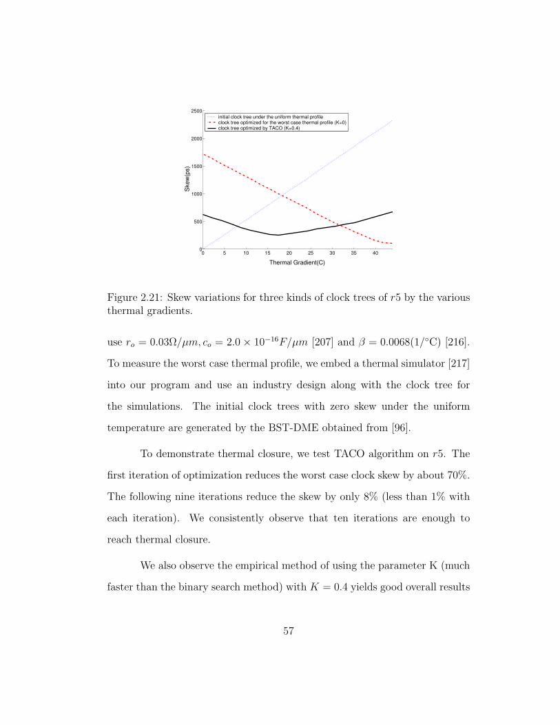
0 5 10 15 20 25 30 35 400
500
1000
1500
2000
2500
Thermal Gradient(C)
Ske
w(p
s)
initial clock tree under the uniform thermal profileclock tree optimized for the worst case thermal profile (K=0)clock tree optimized by TACO (K=0.4)
Figure 2.21: Skew variations for three kinds of clock trees of r5 by the variousthermal gradients.
use ro = 0.03Ω/µm, co = 2.0 × 10⁻¹⁶F/µm [207] and β = 0.0068(1/C) [216].
To measure the worst case thermal profile, we embed a thermal simulator [217]
into our program and use an industry design along with the clock tree for
the simulations. The initial clock trees with zero skew under the uniform
temperature are generated by the BST-DME obtained from [96].
To demonstrate thermal closure, we test TACO algorithm on r5. The
first iteration of optimization reduces the worst case clock skew by about 70%.
The following nine iterations reduce the skew by only 8% (less than 1% with
each iteration). We consistently observe that ten iterations are enough to
reach thermal closure.
We also observe the empirical method of using the parameter K (much
faster than the binary search method) with K = 0.4 yields good overall results
57

0 1 2 3 4 5 6 7 8 9
x 104
0
1
2
3
4
5
6
7
8
9
x 104
Figure 2.22: Initial clock tree (shown in solid line), and optimized clock tree(shown in dotted line) after TACO of r3.
which are presented in Table 2.4 and 2.5. Table 2.4 shows the delay, skew,
total wirelength, and CPU time under the uniform and the worst case thermal
profile for all the benchmarks before optimization. Last column in Table 2.4
shows the worst case clock skew for each of the benchmarks. In Table 2.4, one
may observe huge skews under the worst case thermal profile.
The improvements and the overhead of the proposed algorithm are
shown in Table 2.5 by comparing the delay, skew, and wirelength between
58

Table 2.4 and Table 2.5. The worst case clock skew is reduced by 50% -
70%. As a penalty, the wirelength is increased by 0.35% on average which is
negligible. Besides, the maximum temperature is slightly reduced. The CPU
time is increased linearly with the number of nodes.
Regarding the sensitivity of the skew to the varying thermal gradients,
Fig. 2.21 shows the clock skew variation for r5 for various thermal gradients.
The zero skew tree under the worst case thermal profile is built by setting
K = 0. It can be observed that the initial clock tree (optimal for the uniform
thermal profile) and the clock tree optimized for the worst case thermal profile
show huge worst case clock skew for highest and lowest thermal gradients re-
spectively. While the two zero skew trees show huge worst case clock skew, the
optimized tree by TACO shows the smallest worst case clock skew. Fig. 2.22
shows the clock routing changes due to TACO in dotted lines. TACO makes
small changes to the initial clock tree.
2.3 Routability-driven Global Routing
As mentioned in the introduction of this chapter, routability or conges-
tion is one of the most classic/fundamental yet critical/difficult design objec-
tives in any technology node, as we have to connects all the devices logically
and physically. Routability can be enhanced in multiple stages in physical
synthesis [29,134,219], but routing is the most effective stage, as it plans wire
distribution and embeds wires under design rules with the accurate pin and
blockage information in hand. Routing consists of two steps, global routing
59
and detailed routing. Global routing plans an approximate path for each net,
while detailed routing finalizes exact DRC-compatible pin-to-pin connections.
As detailed routing cannot capture overall congestion due to fine routing grid
size and numerous design rules, global routing should eliminate congestion
by migrating wires from more to less congested regions with the minimized
overhead in wirelength and via. If global routing fails to satisfy congestion
constraint, it will incur significant design cost, as a chip should be resynthe-
sized not to have any congestion before tape out. Therefore, routability should
be the primary goal of global routing.
The significance of routability in VLSI global routing has led to many
global routing algorithms. Burstein et al. [30] proposed a hierarchical approach
to speed up integer programming formulation for global routing, and Kast-
ner [125] proposed pattern-based global routing. Hadsell et al. [89] presented
the Chi dispersion router based on a linear cost function as well as a predicted
congestion map, and showed better results than [125]. A multicommodity
flow-based global router by Albrecht [5] showed good results and was used in
industry, but at the expense of computational effort. FastRoute [175,176] and
DpRouter [32] achieved high quality solution in small runtime. However, most
of the academic global routers work in 2D (with two layers) to handle a larger
circuit with less computing power and smaller memory, and lack of important
layer assignment.
Layer assignment plays a critical role for routability, timing, crosstalk,
and manufacturability/yield. If an excessive number of wires are assigned to a
60

particular layer, it will aggravate congestion and crosstalk [126,230]. If global
timing critical nets are assigned to lower layers, it will make timing worse
due to narrower wire width/spacing. Biased wire density distribution between
layers can cause a large topography variation as well as a pooling effect after
CMP [53]. Length of antenna can be also reduced by layer assignment [228].
A large number of vias due to poor layer assignment can cause routability/pin
access problem, as via (even extended via) needs larger area as well as wider
spacing than wire. Especially, via minimization becomes more important for a
nanometer design due to manufacturability. With a smaller number of vias, we
can decrease the chance of via failure by increasing the percentage of redundant
via insertion [77,137].
Recent global routing contest in ISPD-2007 [103] attracted 17 teams
from both academia and industry, reflecting the renaissance of routing. It pro-
vided 16 industrial benchmarks (8 for 2D and another 8 for 3D) to emphasize
the importance of routability in global routing and the necessity of via mini-
mization in layer assignment. The contest results in several highly advanced
academic global routers. FGR [190] is based on a Lagrangian relaxation and
Steiner tree reconstruction to achieve high quality solution. ARCHER [171]
adopts also a Lagrangian relaxation technique with congestion history learn-
ing, achieving high quality and fast runtime. NTHU-Route [79] uses a sim-
ilar history-based routing techniques. Differently from these history-based
(broader context of Lagrangian relaxation) global routers, MaizeRouter [103]
relies on efficient edge shifting to reduce the number of violations.
61

In this section, we propose another global router, BoxRouter which
consists two steps, 2D global routing and layer assignment. BoxRouter first
performs a very fast yet effective PreRouting to identify the most congested
regions or boxes. Then, it progressively expands a routing box, and per-
forms efficient progressive integer linear programming (ILP) with adaptive
maze routing within each expanded box (BoxRouting), until the entire circuit
is covered, i.e., all the wires are routed. Effective negotiation-based PostRout-
ing follows BoxRouting for further enhancement. Layer assignment is enabled
by novel and efficient progressive via/blockage aware integer linear program-
ming (ILP). The major contributions include the following.
• We propose a new integer linear programming (ILP) formulation which
is significantly faster and more scalable than the traditional formulation
in [5,237], which makes it practical to apply ILP to solve VLSI routing.
• We observe that a simple PreRouting step can capture the overall con-
gestion, and improve runtime.
• We propose the key BoxRouting idea which efficiently utilizes limited
routing capacities based on box expansion initiated from the most con-
gested region estimated by PreRouting. BoxRouting is efficient in terms
of routability as the wires in the more congested region are routed before
those in the less congested region.
• We propose efficient progressive integer linear programming (ILP) for
62

BoxRouting. In our progressive ILP, only wires between two successive
boxes are routed with L-shape patterns.
• We propose adaptive maze routing based on multi-source multi-target
with bridge model. Our adaptive maze routing uses different routing
strategies inside and outside the box such that routability can be maxi-
mized with minimum wirelength increase.
• We propose simple, yet essential dynamic scaling for robust negotiation-
based PostRouting. This prevents a router from spinning out of control
by balancing a historic cost and a present congestion cost, and ensures
consistent routability improvement over iterations.
• We propose ILP for via/blockage aware layer assignment to handle block-
ages and guarantee the feasibility. Also, we apply a progressive ILP
technique for via/blockage aware layer assignment to enhance runtime.
The rest of the section is organized as follows. In Section 2.3.1, pre-
liminaries are described. Comparison and evaluation of ILP formulations are
presented in Section 2.3.2. In Section 2.3.3, BoxRouter is proposed, followed
by layer assignment Section 2.3.4. Experimental results are discussed in Sec-
tion 2.3.5.
63

Table 2.6: The notations in this section.
vi vertex / global routing cell i
eij edge between vi and vj
mij maximum routing capacity of eij
cij available routing capacity of eij
W (i, s) a set of wires of a net i passing a point s (including pins)
P (i) a set of points in a net i
N(i) a set of pins in a net i (N(i) ⊆ P (i))
C(e) a set of wires crossing an edge e
re the available routing capacity of an edge e
zijk a binary variable set to 1if a wire j of a net i is assigned k layer
lij the layer assigned to a wire j of a net i
Tis the top layer assigned to any wire on a point s ∈ P (i)
Bis the bottom layer assigned to any wire on a point s ∈ P (i)
2.3.1 Preliminaries
2.3.1.1 Global Routing Model
The global routing problem can be modeled as a grid graph G(V,E),
where each vertex vi represents a rectangular region of the chip, so called a
global routing cell (G-cell), and an edge eij represents the boundary between vi
and vj with a given maximum routing capacity mij. All the pins are assumed
to be at the center of the corresponding G-cell. Fig. 2.23 shows how a chip
can be abstracted into a grid graph where mAB = 3. Global routing is to find
paths that connect the pins inside the G-cells through G(V,E) for every net.
2.3.1.2 Global Routing Metrics
The key task of global router is to maximize the routability for success-
ful detailed routing [222]. In addition, wirelength, runtime, and timing are
64

A B
G-cell
(a) real circuit with G-cells
A B3
(b) grid graph for routing
Figure 2.23: A real circuit with netlists can be dissected into multiple gridswhich can be mapped into graph for global routing with routing capacity onan edge.
other important metrics for global router.
• Routability is usually the most important metric for global routing. It
can be estimated by the number of overflows which indicates that routing
demand exceeds available routing capacity [125, 222]. In Fig. 2.23, the
number of overflow between vA and vB is one, as there are four routed
nets, but mAB = 3. Formal definition of overflow can be found in [125].
• Wirelength is an important metric for placement as well as routing.
But, it is less important compared to routability, as most wires are routed
with shortest distances, thus the total wirelength is in general not too
far away from optimum for a reasonable global routing solution [222].
However, there can be huge difference in terms of routability between
two different global routing solutions of similar wirelength.
• Runtime is also an important consideration, as global routing links
placement and detailed routing. A fast global router can feed proper
65

interconnection information to higher level design flow for better design
convergence [175].
• Other objectives such as timing and manufacturability are significant ob-
jectives as well, which will be covered in Section 3.2. Since the focus of
this section is on the core global routing techniques, they are not explic-
itly considered in this work. However, our framework can be extended
to handle them in the future.
2.3.2 Practical Integer Linear Programming for Global Routing
Integer linear programming (ILP) techniques have been believed un-
acceptably slow for global routing in VLSI design, despite that they find the
global optimum for a given instance of a problem. In this section, we propose a
new ILP formulation for global routing, which is inherently different from the
one in [5, 237], and discuss pros/cons of each formulation. In this subsection,
to avoid any confusion, we call the traditional ILP formulation as T-ILP and
our new ILP formulation as N-ILP. Both T-ILP and N-ILP are routability-
driven, but they adopt different formulations, which make big difference in
performance and scalability.
Before the main discussion, we describe Fig. 2.24 for clear explanation
in the following sections. Fig. 2.24 (a) shows two unrouted nets a and b which
are further decomposed into wires (See Section 2.3.3.1): net a has three wires
(wa1, wa2 and wa3), and net b has one wire (wb1). For each wire, we can
enumerate all the possible routing paths, but for simplicity we show only the
66

paths in the minimum length and with the minimum via count as in Fig. 2.24
(b). Each possible routing path is called a routing candidate of a given wire.
In this example, we assume that the routing capacity is 2 for the all the edges
(r12 = 2, r25 = 2, and so forth), thus both Fig. 2.24 (c) and (d) are routable
solutions.
2.3.2.1 T-ILP
T-ILP minimizes the maximum congestion over all the edges. Fig. 2.25
is a T-ILP formulation of Fig. 2.24 (b) where a variable C is set to be larger
than any congestion on any edge (i.e., the upper bound). The routing result
after solving Fig. 2.25 is not Fig. 2.24 (d) but Fig. 2.24 (c), as Fig. 2.24 (d)
has the maximum congestion 1.0 on e45 while Fig. 2.24 (c) has the maximum
congestion 0.5.
Let E be the set of edges in the grid (indexed by e), and let N be
the set of all feasible routing candidates. Furthermore, let L(e) be the set of
routing candidates crossing edge e. Suppose xijk is a binary variable set to 1 if
the k -th routing candidate of wire j of net i is chosen. Then, Fig. 2.26 shows
a general formulation of T-ILP.
Note that the number of routing candidates must be kept small (L-
shape or L/Z-shape path) due to practical limitations (e.g. memory). The
advantages of the T-ILP formulation include:
• As it minimizes the maximum congestion (min-max formulation), it es-
sentially tries to achieve more uniform congestion distribution.
67

a
a
a
b
b
s
wb1
wa1
wa2
wa3
V1 V2 V3
V4 V5 V6
V7 V8 V9
(a) decomposed net a, b
a
a
a
b
b
s
xb11
xb12
xa12
xa11
xa21
xa31
V1 V2 V3
V4 V5 V6
V7 V8 V9
(b) routing candidates
a
a
a
b
b
s
xb12
xa12
xa21
xa31
V1 V2 V3
V4 V5 V6
V7 V8 V9
(c) possible routing A
a
a
a
b
b
s
xb12
xa11
xa21
xa31
V1 V2 V3
V4 V5 V6
V7 V8 V9
(d) possible routing B
Figure 2.24: Example of ILP for global routing with two possible routing solu-tions is shown. Two routing solutions in (c) and (d) are valid w.r.t. the givenrouting capacities, but different in terms of congestion distribution. The onein (c) achieves more uniform congestion distribution. T-ILP prefers routing(c) to routing (d), while N-ILP has no preference.
68

min : C
s.t : xa11, xa12, xa21, xa31, xb11, xb12 ∈ 0, 1
xa11 + xa12 = 1
xb11 + xb12 = 1
xa21 = 1, xa31 = 1
xa11 + xb12 ≤ C
xa21 + xb11 ≤ C
xa11 ≤ C, xa12 ≤ C, xa31 ≤ C
xb11 ≤ C, xb12 ≤ C
Figure 2.25: T-ILP formulation for the example of Fig. 2.24 (b).
min : C
s.t : xijk ∈ 0, 1 ∀(i, j, k) ∈ N∑
k:(i,j,k)∈N xijk = 1 ∀i, j∑
(i,j,k)∈L(e) xijk ≤ C ∀e
Figure 2.26: General T-ILP formulation.
• A solution to a T-ILP formulation always includes one routing candidate
for each unrouted wire. Thus, it completes routing by itself, and does
not need any additional step, unless there is any over-congested edge.
Meanwhile, the drawbacks of the T-ILP formulation include:
• When C in Fig. 2.26 is larger than any me (the maximum routing ca-
pacity of the edge e), the number of over-congested edges will explode.
It considers not the overall congestion but the maximum congestion.
69

max : 2xa11 + 2xa12 + xa21 + xa31 + 2xb11 + 2xb12
s.t : xa11, xa12, xa21, xa31, xb11, xb12 ∈ 0, 1
xa11 + xa12 ≤ 1
xb11 + xb12 ≤ 1
xa21 ≤ 1, xa31 ≤ 1
xa11 + xb12 ≤ 2
xa21 + xb11 ≤ 2
xa11 ≤ 2, xa12 ≤ 2, xa31 ≤ 2
xb11 ≤ 2, xb12 ≤ 2
Figure 2.27: N-ILP formulation for the example of Fig. 2.24 (b).
Therefore, as long as the congestion is smaller than C, it is possible to
have many over-congested edges.
• All the over-congested edges should be taken care of to meet conges-
tion constraints (otherwise, it is unroutable by detailed router) by post-
processing steps such as ripup&rerouting.
• A T-ILP formulation cannot be efficiently solved with branch-and-bound
or branch-and-cut algorithms. This will be explained in Section 2.3.2.3.
2.3.2.2 N-ILP
Our proposed N-ILP maximizes the weighted summation of the number
of routed wires under the routing capacity constraint. Fig. 2.27 is a N-ILP
formulation of Fig. 2.24 (b) where each routing candidate is weighted by its
length in the objective. The result from Fig. 2.27 can be either Fig. 2.24 (c)
70

max :∑
(i,j,k)∈N aijk · xijk
s.t : xijk ∈ 0, 1 ∀(i, j, k) ∈ N∑
k:(i,j,k)∈N xijk ≤ 1 ∀i, j∑
(i,j,k)∈L(e) xijk ≤ ce ∀e
Figure 2.28: General N-ILP formulation.
or Fig. 2.24 (d), as N-ILP does not care about the maximum congestion, as
long as there is no overflow. Fig. 2.28 shows the general formulation of N-ILP
where aijk is the weight of the routing candidate xijk and the other notations
are the same as in Fig. 2.26. Again, the number of routing candidates should
be kept small (L-shape or L/Z-shape path). The advantages of the N-ILP
formulation include:
• As each candidate xijk can have a different weight, other design objec-
tives like timing can easily be incorporated.
• Due to the hard constraint on routing capacity, the solution from N-ILP
does not cause any over-congestion on any edge.
• N-ILP can be efficiently solved with branch-and-bound or branch-and-
cut algorithms. This will be explained in Section 2.3.2.3.
However, the drawbacks of the N-ILP formulation include:
• N-ILP may produce a biased routing solution in terms of congestion
uniformness. For example, if there are two valid solutions with different
71

congestion distributions, it may choose any of both depending on the
solver regardless of congestion uniformness (See Fig. 2.24).
• Different from T-ILP, it may not complete the routing. If the over-
congested edge appears, it will give up routing some wires with smaller
weights not to violate the hard routing capacity constraints. Thus, N-
ILP requires an additional step for complete routing.
2.3.2.3 T-ILP vs. N-ILP
Based on the discussion in Section 2.3.2.1 and 2.3.2.2, we compare both
ILP formulations in two aspects: routability and runtime.
As mentioned earlier, both T-ILP and N-ILP maximize the routabil-
ity, but in different manners: T-ILP minimizes the maximum congestion, but
N-ILP maximizes the number of routed wires under the routing capacity con-
straint. This difference becomes highly distinct, depending on whether the
design is under-congested or over-congested.
• For under-congested designs, it is easy for T-ILP and N-ILP to sat-
isfy the routing constraint. Therefore, T-ILP may be superior to N-ILP,
as it can make more uniform congestion distribution which improves
manufacturability and crosstalk noise.
• For over-congested designs, T-ILP may unnecessarily cause a lot of
overflows, as it only cares about the maximum congestion. However,
N-ILP itself does not cause any over-congested edges by leaving some
72

wires unrouted. The overflows from T-ILP and the unrouted wires from
N-ILP need to be picked up by the following maze routing.
Since modern VLSI designs are highly congested in general, the advan-
tage of T-ILP is quite trivial.
For a given ILP solver, different ILP formulations may have different
runtime complexities. An ILP problem is first solved as linear programming
(LP), then a branch based algorithm is applied to any fractional variable to
find an integral optimal solution. We find that for the most widely used ILP
solving algorithms, branch-and-bound or branch-and-cut [102,225], the N-ILP
formulation can be solved much more efficiently than the T-ILP formulation
for the same routing problem.
For demonstration purpose, we prepare various routing problems in
different problem sizes (in terms of the number of variables), then formulate
them into both T-ILP and N-ILP. Fig. 2.29 shows the normalized runtime of
each T-ILP and N-ILP formulation under a typical computing environment
(See Section 2.3.5) with GNU Linear Programming Kit (GLPK) 4.8 with all
speedup options turned on. Note that we obtain very similar trend for various
algorithms such as branch-and-bound and branch-and-cut with different cut-
ting planes [74, 102]. It is clear that N-ILP is significantly faster than T-ILP,
and such speedup becomes more significant for larger problems, e.g., over 1100
times for some large cases. There are two theoretical explanations why N-ILP
can be solved much faster than T-ILP.
73

• Since N-ILP is similar to a binary knapsack formulation, the solution af-
ter LP is a near feasible solution with almost all variables non-fractional [169,
225]. However, due to the min-max nature of the objective function,
the variables in T-ILP have more incentive to remain fractional after LP
as opposed to their counterparts in N-ILP. Consequently, the LP solu-
tion of T-ILP is much more fractional than that of N-ILP, resulting in
more branches during branch-and-bound or branch-and-cut.
• The branch-and-bound or branch-and-cut techniques terminate in shorter
time, if more nodes can be fathomed [225]. Unfortunately, the min-max
nature of the objective function in T-ILP results in many near optimal
solutions. Therefore, the corresponding nodes cannot be fathomed effi-
ciently and the branch tree grows needlessly.
N-ILP is significantly faster than T-ILP, and the solution quality from
N-ILP is similar to that from N-ILP for an over-congested design. Thus, N-
ILP is expected to work better for modern VLSI designs. Our proposed N-ILP
is adopted in BoxRouter in Section 2.3.3, in a progressive manner with a box
expansion concept.
2.3.3 BoxRouter
In this subsection, we present our new global router, BoxRouter, which
is based on congestion-initiated box expansion. BoxRouter progressively ex-
pands a box which initially covers the most congested region only, but finally
74

0 0.5 1 1.5 2 2.5 3 3.5 4 4.5 5
x 104
10−1
100
101
102
103
104
No
rma
lize
d r
un
tim
e (l
og
sca
le)
Problem size
T−ILP
N−ILP
1135 times
Figure 2.29: Runtimes of T-ILP and N-ILP are compared. It shows that N-ILPis much faster and more scalable for larger problems than T-ILP.
covers the whole circuit. After every expansion, a circuit is divided into two
sections, inside the box and outside the box. BoxRouter uses different routing
strategies for each section to maximize routability and minimize wirelength.
Consider Fig. 2.30 (a), where two wires (a and b) are inside the box, while the
other wires (c and d) are not inside the box. The routing capacity inside the
box is more precious to a and b than c and d for two reasons:
• If a and b are not routed within the box, wirelength will increase due to
detour.
• c and d may have another viable routing path outside box which does
not waste the routing capacity inside the box.
75

d
d
c
c
a
a
b
b
(a) motivation for BoxRouting
Keep dense with
greedy strategy
Keep uniform with
conservative strategy
Box
(b) strategies of BoxRouting
Figure 2.30: The basic concept of BoxRouter.
Therefore, BoxRouter first routes as many wires inside the box as possible
with N-ILP in Section 2.3.2.2, maximally utilizing the routing capacity inside
the box. Then, for the wires which cannot be routed by N-ILP within the box
(due to insufficient routing capacities), BoxRouter detours them by adaptive
maze routing with the following two strategies:
• Inside the box, use the routing capacities as many as possible (greed-
ily), as the wires inside the box have priority over those outside the box.
• Outside the box, use the routing capacities conservatively, as the wires
outside the box may need them later for their viable routing paths.
Those two strategies keep the wire density of the circuit as in Fig. 2.30 (b),
and make wires detour the more congested regions to maximize routability
with minimum wirelength overhead.
76

PreRoute & Initial Box
Progressive ILP Routing
Adaptive Maze Routing
Box Expansion
all wires routed?
PostRoute
Bo
xR
ou
te
Minimum Steiner Tree
Y
Net Decomposition
N
Bo
xR
ou
terFigure 2.31: BoxRouter consists of three main steps: PreRouting, BoxRouting,and PostRouting. BoxRouting can be further composed of progressive ILP andadaptive maze routing.
The overall flow of BoxRouter is in Fig. 2.31, which will be explained in
detail in the rest of this subsection. Section 2.3.3.1 describes the preprocessing
for BoxRouter. Section 2.3.3.2 illustrates PreRouting for congestion estimation
and routing speedup. Section 2.3.3.3 explains BoxRouting, the main idea
of BoxRouter which includes progressive ILP (PILP), adaptive maze routing
(AMR), and box expansion. Finally, Section 2.3.3.4 shows how PostRouting
improves wirelength and routability.
77

net a-b-c-d
a
d
b
c
(a) hypergraph for a net
d
wire a-ewire e-d
wire b-f wire f-c
wire e-f
f
e
a
c
b
(b) wires after decomposition
Figure 2.32: Net can be decomposed into two pin wires with Rectilinear Min-imum Steiner Tree Construction.
2.3.3.1 Steiner Tree and Net Decomposition
A net can be decomposed into two pin wires with Rectilinear Min-
imum Steiner Tree as shown in Fig. 2.32. In BoxRouter, Flute [63] and
GeoSteiner [100, 218] are tested for Steiner tree construction, but Flute is
finally adopted due to its small computational overhead. Note that different
Steiner tree algorithms such as timing-driven or congestion-driven Steiner tree
algorithms can be used in BoxRouter as well. A special wire which does not
need a bend is called a flat wire [147]. For example, wire a-e, e-d, e-f and b-f
in Fig. 2.32 (b) are flat wires, while wire f-c requires at least one bend to be
routed. Each wire from a net becomes a single routing object. However, the
net is finally routed, only if all the wires from a net are routed. Routing each
wire from a single net separately may have a downside of loosing information
on other wires, resulting in suboptimal routing. This issue is addressed in
adaptive maze routing in Section 2.3.3.3.2.
78
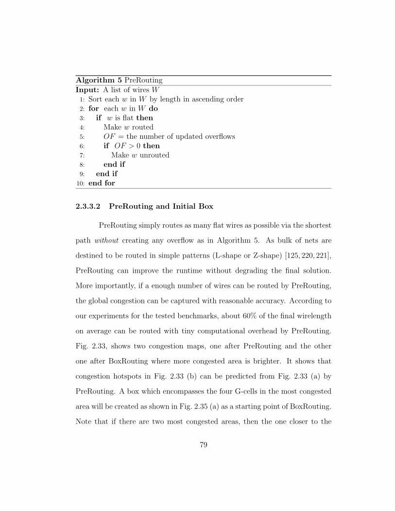
Algorithm 5 PreRouting
Input: A list of wires W1: Sort each w in W by length in ascending order2: for each w in W do3: if w is flat then4: Make w routed5: OF = the number of updated overflows6: if OF > 0 then7: Make w unrouted8: end if9: end if
10: end for
2.3.3.2 PreRouting and Initial Box
PreRouting simply routes as many flat wires as possible via the shortest
path without creating any overflow as in Algorithm 5. As bulk of nets are
destined to be routed in simple patterns (L-shape or Z-shape) [125, 220, 221],
PreRouting can improve the runtime without degrading the final solution.
More importantly, if a enough number of wires can be routed by PreRouting,
the global congestion can be captured with reasonable accuracy. According to
our experiments for the tested benchmarks, about 60% of the final wirelength
on average can be routed with tiny computational overhead by PreRouting.
Fig. 2.33, shows two congestion maps, one after PreRouting and the other
one after BoxRouting where more congested area is brighter. It shows that
congestion hotspots in Fig. 2.33 (b) can be predicted from Fig. 2.33 (a) by
PreRouting. A box which encompasses the four G-cells in the most congested
area will be created as shown in Fig. 2.35 (a) as a starting point of BoxRouting.
Note that if there are two most congested areas, then the one closer to the
79

(a) congestion after PreRouting (b) congestion after BoxRouting
Figure 2.33: Congestion estimations after PreRouting and BoxRouting arecompared. It shows that simple PreRouting can effectively capture overallcongestion as well as the most congested region.
center of the circuit is selected.
2.3.3.3 BoxRouting
In this subsection, BoxRouting will be explained with Fig. 2.35. BoxRout-
ing consists of three steps, progressive integer linear programming routing,
adaptive maze routing, and box expansion as in Fig. 2.31. These three steps
are repeated until the expanded box covers the whole circuit, which will be
explained in the following subsections.
2.3.3.3.1 Progressive ILP (PILP) Routing We show in Section 2.3.2
that N-ILP is more efficient than T-ILP for modern, typically over-congested
VLSI designs. Therefore, we use N-ILP formulation in PILP and further ex-
tend it by combining with the box expansion concept.
80

max :xb1 + xb2 + xf1 + xf2 + xh1 + xh2
s.t :xb1, xb2, xf1, xf2, xh1, xh2 ∈ 0, 1
xb1 + xb2 ≤ 1
xf1 + xf2 ≤ 1
xf2 = 0
xh1 + xh2 ≤ 1
xb1 + xf1 + xh1 ≤ cAB
xb1 + xh1 ≤ cBD
xb2 + xh2 ≤ cAC
xb2 + xh2 ≤ cCD
Figure 2.34: Progressive ILP formulation of Fig. 2.35 (c).
Assuming a box is expanded from the most congested region as in
Fig. 2.35 (a), consider Fig. 2.35 (b), where wires within the box after i -th
expansion (box i) are shown with squares (b, f and h), and the other wires are
shown with circles. The already routed wires by either PreRouting or previous
BoxRouting are simply shown as solid lines. Note that some flat wires like f, i,
and k could be remained unrouted until BoxRouting, if PreRouting gives up
routing them due to any overflow, or new Steiner points introduced by adaptive
maze routing (AMR) (explained later in this section) convert a non-flat wire
into a flat wire. For efficient routing as mentioned in the beginning of this
subsection, only wires within the box will be routed by PILP and AMR.
In Fig. 2.35 (c), the wires within the box are shown with G-cells
(vA, vB, vC and vD), and the corresponding PILP formulation for maximum
routability is shown in Fig. 2.34. To minimize the number of vias, two L-
81

(a)
Init
ial
box
iscr
eate
don
the
hot
spot
whic
his
esti
mat
edby
Pre
-R
outi
ng.
a
a c
c
d
d
ii
kkf
f
b
b
h
h
Bo
x i
(b)
Box
iw
ith
wir
esw
hic
hw
ill
be
route
dby
Box
Rou
ting
issh
own.
ff
b
b
h
h
vAvB vD
vC
xb1
xb2
xf1
xh2
xh1
Bo
xi
(c)
Wir
esw
ithin
Box
iw
ill
be
route
dby
pro
gres
sive
ILP.
a
a c
c
d
d
ii
kkf
f
b
b
h
h
Bo
x i
(d)
Unro
ute
dw
ire
baf
ter
pro
-gr
essi
ve
ILP
isro
ute
dby
adap
-ti
ve
maz
ero
uti
ng.
a
ab
b
ff
h
h
ii
d
d
kk
c
c
Bo
x i
Bo
x i
+1
(e)
Box
iis
expan
ded
,an
dm
ore
wir
esar
een
clos
edby
Box
i+1.
a
ab
b
ff
h
h
ii
d
d
kk
c
c
Box i
Box i
+1
(f)
Box
Rou
ting
isper
form
edw
ith
Box
i+1.
Fig
ure
2.35
:B
oxR
outi
ng
exam
ple
.
82

max :∑
xi1 + xi2 ∀i ∈ Wbox
s.t :xi1, xi2 ∈ 0, 1 ∀i ∈ Wbox
xi1 + xi2 ≤ 1 ∀i ∈ Wbox
xi2 = 0 ∀i ∈ Wbox ∩ Wflat∑
e∈xi,j
xij ≤ ce ∀e ∈ Wbox
Figure 2.36: General progressive ILP formulation.
shape routing candidates (xb1, xb2 and xh1, xh2) are considered for each wire
in our PILP formulation, but only one routing candidate (xf1 and xf2=0) is
considered for flat wires. A general PILP formulation is shown in Fig. 2.36,
where ce is the available routing capacity on edge e (See Table 2.6), Wbox is a
set of unrouted wires within the current box, and Wflat is a set of flat wires.
Differently from the hierarchical ILP [30], our PILP progressively routes
a part of the circuit, which is covered by each expanding box. This box
expansion limits the problem size such that PILP which is NP-hard can be
solved efficiently. Three advantages of our PILP can be summarized as follows:
• The basic formulation is the same as N-ILP of Section 2.3.2.2, inheriting
its advantages in runtime and scalability.
• Even though the last box can cover the whole circuit, the PILP size
remains tractable, as N-ILP is performed on the wires between two suc-
cessive boxes like between Box i and Box i+1 in Fig. 2.35 (e).
83

Algorithm 6 BoxRouting
Input: A list of wires W in box B1: Solve progressive ILP with W2: for each w in W do3: if w is unrouted then4: Perform adaptive maze routing for w5: end if6: end for
• As shown in Fig. 2.35 (e), the newer box always contains the older box.
Consequently, the solution from the older PILP is reflected in the newer
PILP formulation, providing smooth transition between two successive
problems for a high quality solution.
Due to the limited routing capacity of each edge, some wires may not
be routed with the above PILP. xi1 + xi2 ≤ 1 in Fig. 2.36 relaxes the routing
constraint such that some wires may not be routed if the overflow occurs. For
example, assuming mBD = mCD = 2 and xh1 = 1, the wire b cannot be routed
with ILP (xb1 = xb2 = 0), as two prerouted wires on eCD, and one prerouted
wire with the wire h (xh1 = 1) on eBD consume all the routing capacities. For
this case, the wire b is routed by AMR as in Fig. 2.35 (d) with the routing
cost from Algorithm 7.
2.3.3.3.2 Adaptive Maze Routing (AMR) Algorithm 7 returns a unit
cost as long as eXY is inside box and still has available routing capacity (line
2, 3). Otherwise, it returns a cost inversely proportional to the available rout-
ing capacities (line 1). This cost function makes maze routing adaptively find
84

S T b
ac
x y
path1
path2
path3
(a) by finding shorter path x-y
TS
bcx y
a
path1
path2 path3
(b) by sharing routed path x-y
Figure 2.37: Efficient multi-source multi-target maze routing examples areillustrated. More efficient alternative paths are found by considering multiplesources and targets.
the best routing path such that the shortest path inside the box for wirelength
minimization, but the most idle path outside the box for routability maximiza-
tion. Note that the resource outside the box should be used conservatively, as
the wires outside the current box may need them later. If too big detour is
required to avoid small overflows, AMR may return a path with overflows for
the least overall cost.
For maze router implementation, we propose a multi-source multi-
target with bridge (MMB) maze routing model for higher efficiency as illus-
trated in Fig. 2.37. Consider the example in Fig. 2.37 (a) where a source G-cell
S and a target G-cell T are to be connected and the congestion is represented
as shaded region. To avoid congestion, a simple maze routing can easily find
the routing path path2 instead of path1. However, as the goal is to make S
and T electrically connected, we can achieve electrical connection as well as
85

Algorithm 7 Adaptive Maze Routing Cost for BoxRouting
Input: G-cell Vx, Vy, Box B1: Cost C = mxy − cxy
2: if exy is inside B and cxy > 0 then3: C = 14: end if
Output: C
shorter wirelength by alternatively routing x and y shown as path3. The other
example in Fig. 2.37 (b) shows the case where the routing between b and c is
detoured due to congestion. In this case, even though path1 is the shortest
path between S and T without any congestion issue, the path S-x-y-T shown
as path2− path3 is the better routing path, because it shares and utilizes the
existing routed path path3, resulting in the shorter total wirelength.
Aware of the above mentioned cases, the proposed multi-source multi-
target with bridge (MMB) based maze routing in Fig. 2.38 is implemented for
AMR. The basic idea behind MMB is to make the maze router honor existing
partial routed paths of the net for shorter wirelength and less congestion. In
detail, the proposed model is based on three different groups of G-cells as in
Fig. 2.38.
• Source group: a group of G-cells which are electrically connected to
the source G-cell S.
• Target group: a group of G-cells which are electrically connected to
the target G-cell T .
86

S
T
source grouptarget group
bridge group 1
bridge group 2
bridge group 3
Figure 2.38: Multi-source multi-target with bridge maze routing model.
• Bridge group: multiple groups of G-cells on the partial routing paths
which are connected to neither the source S nor the target T .
Note that identifying each group of G-cells can be done with any graph
traversal algorithm with trivial computational overhead. There can be multi-
ple bridge groups in case that many routed paths (from PreRouting or previous
AMR) are not connected with each other.
Flooding of maze routing is started from the all the G-cells in the
source group, and is terminated when any G-cell in the target group with the
minimal cost is discovered. Flooding within a bridge group is free by treating
one bridge group as a single virtual G-cell to encourage higher utilization
of existing routed paths for shorter total wirelength. Details on AMR is in
Algorithm 8.
It should be noted that MMB based maze routing may change the initial
Steiner tree structure according to the congestion updated during routing, and
this may negatively affect the runtime as a maze router needs to search a
87

Algorithm 8 Adaptive Maze Routing
Input: Source s and target t of net N with box B1: Find source group Gs of s2: Find target group Gt of t3: Find all bridge groups Gb1, Gb2, ... of N4: A priority queue Q = φ5: for each G-cell Vx in Gs do6: Cost Tx of Vx = 07: Enqueue Vx into Q8: end for9: Best target G-cell Vb = φ, Tb = ∞
10: while Q is not empty do11: dequeue a G-cell Vx from Q12: if Tx ≥ Tb then13: break14: end if15: for each adjacent G-cell Vy of Vx do16: Tn = Algorithm 7 (Vx, Vy, B)17: Ty = Tx + Tn
18: if Vy ∈ Gt and Ty < Tb then19: Vb = Vy, Tb = Ty
20: else if Vy ∈ Gbi then21: for each G-cell Vz in Gbi do22: Tz = Ty
23: Enqueue Vz into Q24: end for25: else26: Enqueue Vy into Q27: end if28: end for29: end while30: P = Backtrace the best path from Vb to any G-cell of Gs
Output: P
88

larger area for the optimal routing path. This runtime issue can be mitigated
if a congestion-driven Steiner tree algorithm is adopted. Note that a simple
wirelength driven Steiner tree algorithm is assumed in this work.
2.3.3.3.3 Box Expansion After all the wires inside the box i are routed
either by PILP or AMR, the box i will be expanded to the box i+1, and new
wires (c, d and k) are encompassed by the box i+1 as shown in Fig. 2.35 (e).
The result after applying BoxRouting (AMR after PILP) again is shown in
Fig. 2.35 (f). The amount of increment during box expansion significantly
affects the routing solution. As the box grows larger for every expansion
with bigger increment, the runtime increases exponentially due to the larger
PILP problem size (more wires are added into the formulation due to larger
expansion). However, the smaller overflow can be obtained, as the routing
is performed more globally. There can be several heuristics to determine the
increment such as constant increment size or dynamic increment size, but
it is required to keep PILP problem size manageable. After all wires are
routed (the box becomes big enough to cover the whole circuit), PostRouting
of Section 2.3.3.4 will follow BoxRouting. Each wire in the box is optimally
routed by PILP, but the global optimality is not guaranteed as box expands.
To certain extend, BoxRouting mimics the diffusion effect which was
originally proposed for placement migration in [186]. By each BoxRouting
step, all the wires in the more congested region (within the box) are routed
first by PILP, then by AMR. This makes the wires outside the box detour the
89

box, if necessary. Such box expansion and congestion spreading diffuse wires
in a progressive and systematic manner.
Our box expansion can be initiated from multiple regions, in case there
are several congestion hotspots. This may lead to better congestion distribu-
tion as well as improved runtime. As the key idea behind box expansion is to
diffuse wires from more congested regions to less congested regions, intuitively
multiple box expansion has advantages. More importantly, multiple box ex-
pansion can be effectively performed on a multiprocessor/distributed comput-
ing environment owing to two reasons: a) most commercial ILP solvers itself
support such computing environments; b) each PILP can be solved indepen-
dently as long as boxes are not overlapped. However, several implementation
issues such as where to begin (how to define congestion hotspot) and when to
stop should be addressed with well-tuned heuristics.
2.3.3.4 PostRouting with Negotiation
PostRouting is to further improve the solution quality by eliminating
any remaining overflows or reducing wirelength in an iterative manner. Instead
of maze routing/shortest path algorithms, we adopt the A∗ search algorithm
and use the following cost function during PostRouting:
costi(e) = hi(e) + αp(e) + βd(e) (2.9)
where regarding an edge e, hi(e) is a historic cost at i-th iteration, p(e) is a
present congestion cost, and d(e) is the distance from e to the target.
90
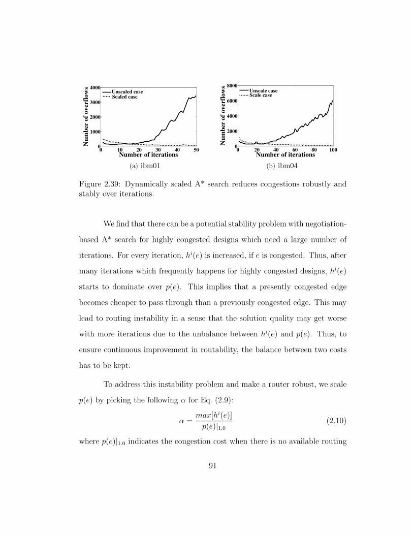
0 10 20 30 40 500
1000
2000
3000
4000
Number of iterations
Nu
mb
er o
f over
flow
sUnscaled caseScaled case
(a) ibm01
0 20 40 60 80 1000
2000
4000
6000
8000
Number of iterations
Nu
mb
er o
f over
flow
s
Unscale caseScale case
(b) ibm04
Figure 2.39: Dynamically scaled A* search reduces congestions robustly andstably over iterations.
We find that there can be a potential stability problem with negotiation-
based A* search for highly congested designs which need a large number of
iterations. For every iteration, hi(e) is increased, if e is congested. Thus, after
many iterations which frequently happens for highly congested designs, hi(e)
starts to dominate over p(e). This implies that a presently congested edge
becomes cheaper to pass through than a previously congested edge. This may
lead to routing instability in a sense that the solution quality may get worse
with more iterations due to the unbalance between hi(e) and p(e). Thus, to
ensure continuous improvement in routability, the balance between two costs
has to be kept.
To address this instability problem and make a router robust, we scale
p(e) by picking the following α for Eq. (2.9):
α =max[hi(e)]
p(e)|1.0
(2.10)
where p(e)|1.0 indicates the congestion cost when there is no available routing
91

capacity in an edge e. Insight behind such α is to make passing presently
congested edge (no more routing capacity available) as expensive as passing
previously congested edge. This will discourage creating new overflows, while
avoiding previously congested edges.
Fig. 2.39 shows the effect of robust negotiation-based A* search by
comparing the scaled case (Eq. (2.10)) and the unscaled case (α=1) on two
benchmark circuits. For the unscaled case, it reduces the number overflows
faster than the scaled case for a while, but after a certain point, it spins a
router out of control and increases the number of overflows. This implies
that if circuit is too hard to be routed in a few iterations, a router becomes so
unstable that it cannot improve the routing quality. Meanwhile, the scaled case
stably reduces the number of overflows even after a large number of iterations.
With larger α, we may delay spinning out of control, but it will eventually
occur after a larger number of iterations.
When a wire is selected for rerouting, we explore larger flexibility by
ripping up some adjacent wires in the same net, while honoring the current
routing topology. The reason we need to honor the current topology is because
an abrupt change in a congestion map can misguide a router with inaccurate
congestion estimation.
Consider the example in Fig. 2.40 where pins are in circle (a, b, c, d, e)
and Steiner points are in square (1, 2, 3, 4, 5, 6). As wire 3-4 in Fig. 2.40 (a)
is passing through a congested region in dark area, it will be ripped up for
rerouting. Moreover, two connected wires, wire b-3 and 4-5 are ripped up
92

a 1
b
c
2
4 5
d
6 e
3
(a) before wire ripup
a 1
b
c
2
5
d
6 e
(b) after wire ripup
Figure 2.40: Topology aware wire ripup improves routing flexibility by rippingup some connected wires, but honors the current routing topology.
together as shown in Fig. 2.40 (b). The motivation behind our ripping up is
that a Steiner point (which is not a pin) with degree two such as Steiner points
3 and 4 are not critical in terms of routing topology, as they simply bridge
two wires. Thus, ripping up wire b-3-4-5 provides more flexibility in terms of
rerouting, while honoring the current routing topology.
2.3.4 Layer Assignment
In this subsection, we propose a layer assignment for via-minimization
based on progressive integer linear programming (PILP). When 2D global rout-
ing is finished, layer assignment follows to distribute the wires across the layers.
Layer assignment impacts several design objectives, such as timing, noise, and
manufacturability, but our layer assignment mainly focuses on via minimiza-
tion without altering routing topology. This problem is known as constrained
via minimization (CVM) [2,37,38] which is shown as NP-complete [163]. How-
ever, our layer assignment for via minimization inherently differs from previous
93

a1 a2b2 b3
b5c1
b6b4
b1
A B C
D
F G H
x
y
c3
E
c2
(a) 2D global routing result for neta,b, and c with blockages when M1-M4 are superposed
a1 a2b2 b3
b5c1
b6b4
b1
13 vias
yy
xx
c3
c2
(b) suboptimal via aware layer as-signment of 13 vias with blockage xand y on M4
a1 a2b2 b3
b5 b6b4
b1
11vias
y
c1 c2
c3
xx
(c) optimal via aware layer assign-ment of 11 vias with blockage x andy on M4
a1 a2b2 b3
b5 b6b4
b1
15 vias
xy
c1 c2
c3
(d) optimal via aware layer assign-ment of 15 vias with blockage x onM2 but y on M4
Figure 2.41: Layer assignment can determine the number of vias as shown in(b) and (c). Also, the location of blockages in 3D can affect routability in (d).
works in two aspects.
• Multiple wires can be overlapped, if there are enough routing capacities
between G-cells, while CVM does not allow due to DRC.
• Wires can be splitted into multiple pieces to avoid blockages, while CVM
cannot.
94

min :∑
i
∑
s∈P (i)(Tis − Bis)
s.t : (a) zijk ∈ 0, 1 ∀i, j, k
(b)∑
k zijk = 1 ∀i, j, k
(c)∑
k k · zijk = lij ∀i, j, k
(d) Bis ≤ lij ≤ Tis ∀(i, j) ∈ W (i, s)
(e) Bs = M1 ∀s ∈ N(i)
(f)∑
(i,j,k)∈C(e) zijk ≤ re ∀e
Figure 2.42: ILP formulation for via aware layer assignment.
2.3.4.1 Via aware Layer Assignment
Depending on layer assignment, the number of vias can be significantly
different. Fig. 2.41 shows an example of layer assignment for via minimization,
where net a, b, and c are routed through 2D global routing cells, and pins are
shown in circle, while a Steiner point (c2) in square. The example assumes
four metal layers (M1-M4), where M1 and M3 are for horizontal wires, M2
and M4 are for vertical wires, and all the pins on M1. Further, a single
routing capacity is assumed for each edge. If a greedy approach (a shorter net
is assigned to lower layer) is adopted, it will result in Fig. 2.41 (b) with 13
vias. However, Fig. 2.41 (b) has 2 more vias (18% overhead) than the optimal
assignment in Fig. 2.41 (c). This is simply because the greedy approach cannot
capture the global view. Hence, we propose an integer linear programming
(ILP) for via aware layer assignment shown in Fig. 2.42 where notations are
in Table 2.6 in Section 2.3.1.
95
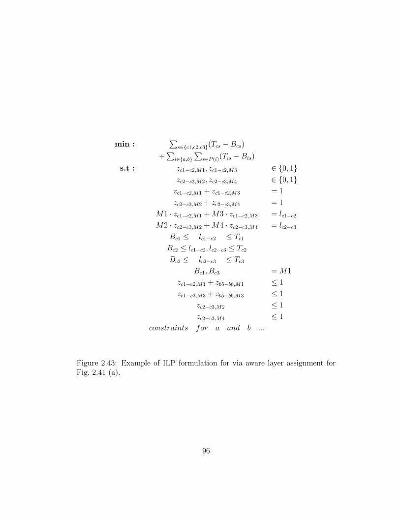
min :∑
s∈c1,c2,c3(Tcs − Bcs)
+∑
i∈a,b
∑
s∈P (i)(Tis − Bis)
s.t : zc1−c2,M1, zc1−c2,M3 ∈ 0, 1
zc2−c3,M2, zc2−c3,M4 ∈ 0, 1
zc1−c2,M1 + zc1−c2,M3 = 1
zc2−c3,M2 + zc2−c3,M4 = 1
M1 · zc1−c2,M1 + M3 · zc1−c2,M3 = lc1−c2
M2 · zc2−c3,M2 + M4 · zc2−c3,M4 = lc2−c3
Bc1 ≤ lc1−c2 ≤ Tc1
Bc2 ≤ lc1−c2, lc2−c3 ≤ Tc2
Bc3 ≤ lc2−c3 ≤ Tc3
Bc1, Bc3 = M1
zc1−c2,M1 + zb5−b6,M1 ≤ 1
zc1−c2,M3 + zb5−b6,M3 ≤ 1
zc2−c3,M2 ≤ 1
zc2−c3,M4 ≤ 1
constraints for a and b ...
Figure 2.43: Example of ILP formulation for via aware layer assignment forFig. 2.41 (a).
96

The objective is to minimize the difference between the top layer and
bottom layer used by wires of each net for each point. The constraint (b) is
to assign a wire j of a net i to one of the layers. lij of the constraint (c) is
computed by the combination of zijk. Then, Tis and Bis are captured by the
constraint (d). If there is a pin on s, Bis is set as M1 in the constraint (e).
Finally, all the layer assignment cannot violate the capacity constraints of all
the edges by (f). Fig. 2.43 shows the ILP formulation for Fig. 2.41 (a), mainly
focusing on the net c. Although the proposed ILP formulation can optimally
minimize the number of vias during layer assignment, it has two drawbacks:
• Depending on blockage locations, the formulation can be infeasible, which
will be addressed in Section 2.3.4.2.
• ILP inherently cannot be applied for large designs. Thus, it needs a
technique to improve the speed, which will be discussed in Section 2.3.4.3.
2.3.4.2 Via/Blockage aware Layer Assignment
Since the exact layer information on blockages is diluted in 2D global
routing, layer assignment based on the 2D routing result may not be feasible.
Compare Fig. 2.41 (c) and Fig. 2.41 (d), where the blockage x is located in
different layers. In Fig. 2.41 (c), both x and y are on M4, enabling to route
wire b1 − b4 on M2. However, in Fig. 2.41 (d), wire b1 − b4 cannot be routed
as it is, as x is on M2 while y is on M4. Wire b1− b4 should be chopped into
two pieces such that it can shuttle from M2 to M4 as in Fig. 2.41 (d). Thus,
97

min :∑
i
∑
s∈P (i)(Tis − Bis) − α∑
i,j,k zijk (α ≫ 1)
s.t : zijk ∈ 0, 1 ∀i, j, k∑
k zijk ≤ 1 ∀i, j, k∑
k k · zijk = lij ∀i, j, k
Bis ≤ lij ≤ Tis ∀(i, j) ∈ W (i, s)
Bis = M1 ∀s ∈ N(i)∑
(i,j,k)∈C(e) zijk ≤ re ∀e
Figure 2.44: ILP formulation for via/blockage aware layer assignment.
unless wire b1− b4 is splitted in advance, the formulation in Fig. 2.42 becomes
infeasible. This issue can be easily addressed by chopping wires wherever a
blockage exits, but this may result in not only unnecessary vias but also too
many variables in ILP. Therefore, it is better to break a wire only if needed.
Motivated by the idea in Section 2.3.2, we propose a new ILP formu-
lation for via/blockage aware layer assignment as shown in Fig. 2.44, where
the constraint (b) in Fig. 2.42 is relaxed, and the objective is modified. This
formulation is guaranteed to be feasible for any blockage distribution. In fact,
the new formulation does not require layer assignment for all wires, but the
objective is to complete as many wires as possible, while minimizing the num-
ber of vias. The unassigned wires after solving ILP will be picked up by a
maze routing like in Section 2.3.3.3.2. But, differently from the one in Sec-
tion 2.3.3.3.2, our maze routing is much simpler and faster, because it only
needs to shuttle between layers to finish routing. Therefore, fewer wires will
98

(a) after i-th iteration, all the wiresare layer-assigned by ILP of Fig. 2.44followed by simple maze routing.
ILP solved for wires between boxes
(b) in i+1-th iteration, the wires be-tween two boxes are to be layer-assigned in the same manner.
Figure 2.45: Progressive ILP based on box expansion is efficient in managingproblem size tractable, while honoring the solutions from previous iterations.
be chopped than the approach of chopping all the wires before solving ILP,
resulting in a smaller number of vias in shorter runtime.
2.3.4.3 Progressive ILP for Via/Blockage aware Layer Assignment
ILP is computationally expensive, as most solvers use branch-and-
bound algorithms. Thus, to apply ILP to industrial designs, the problem
size should be tractable, while maintaining the global view. We adopt the
idea of box expansion and the progressive ILP formulation in Section 2.3.3.3
for our layer assignment. Fig. 2.45 illustrates the core idea of progressive ILP.
It starts with a minimal box covering the most congested region. Then, we
solve the problem inside the box (in our case, layer assignment) by ILP as in
Fig. 2.45 (a). After the box expands to cover the larger area, the problem
inside the expanded box is solved in the way as shown in Fig. 2.45 (b). Since,
however, the current problem encloses the previous problem (which has been
solved), the actual problem is limited down to routing only the wires between
99

two consecutive boxes, which in turn makes problem size tractable. Addition-
ally, the previous solution becomes a part of the current problem, thus all the
decisions made previously are honored by the current optimization.
2.3.5 Experimental Results
Table 2.7: ISPD07 IBM benchmarks [103].namea nets grids v.capb h.capb placer
adaptec1 219794 324x324 70 70 Capoadaptec2 260159 424x424 80 80 mPL6adaptec3 466295 774x779 62 62 Dragonadaptec4 515304 774x779 62 62 APlace3adaptec5 867441 465x468 110 110 mFARnewblue1 331663 399x399 62 62 NTUplace 3.0newblue2 463213 557x463 110 110 FastPlace 3.0newblue3 551667 973x1256 80 80 Kraftwerka 2D cases have 2 layers, but 3D cases have 6 layers.b vertical/horizontal capacity
We implement BoxRouter in C++, and perform all the experiments on
a 2.8 GHz Pentium 32bit Linux machine with 2GB RAM. Congestion aware
Steiner tree construction [175] based on Flute [63] is adopted. We use ISPD07
benchmarks to demonstrate BoxRouter. Also, we apply BoxRouter to ISPD98
benchmarks as well, and further modify ISPD98 benchmarks to see the limit
of BoxRouter. Details on ISPD07 and ISPD98 benchmarks are presented in
Table 2.7 and 2.9 respectively.
100

Tab
le2.
8:C
ompar
ison
bet
wee
nIS
PD
07co
nte
stan
ts(i
ncl
udin
gal
lw
inner
s)an
dou
rson
ISP
D07
ben
ch-
mar
ks.
FG
R[1
03]
Mai
zeR
oute
r[1
03]
NC
TU
-R(1
0)[1
03]
Fas
tRou
ter
[103
]B
oxR
oute
rnam
ew
len
am
ax.o
bov
flc
wle
nm
ax.o
ovfl
wle
nm
ax.o
ovfl
wle
nm
ax.o
ovfl
wle
nm
ax.o
ovfl
adap
tec1
.2d
55.8
00
62.2
60
066
.72
417
090
.47
412
258
.37
00
adap
tec2
.2d
53.6
90
057
.23
00
55.4
12
282
.46
1250
055
.69
00
adap
tec3
.2d
133.
340
013
7.75
00
137.
840
020
2.53
00
137.
960
0ad
apte
c4.2
d12
6.05
00
128.
450
010
5.71
00
170.
80
012
7.79
00
adap
tec5
.2d
155.
820
017
6.69
22
187.
2914
6225
1.68
7696
8016
2.11
00
new
blu
e1.2
d47
.51
1012
1850
.93
1613
4854
.41
820
74.1
3219
3451
.13
240
0new
blu
e2.2
d77
.67
00
79.6
40
080
.81
00
114.
950
078
.68
00
new
blu
e3.2
dd10
8.18
1090
3697
011
4.63
1236
3258
811
0.02
1136
1577
015
4.59
1306
3423
611
1.61
1088
3895
8
adap
tec1
.3d
90.9
22
6099
.61
00
--
-24
8.95
412
292
.04
00
adap
tec2
.3d
92.1
950
298
.12
00
--
-24
4.41
1250
094
.28
00
adap
tec3
.3d
203.
440
021
4.08
00
--
-52
3.21
00
207.
410
0ad
apte
c4.3
d18
6.31
00
194.
380
0-
--
469.
340
018
6.42
00
adap
tec5
.3d
264.
582
2480
305.
322
2-
--
707.
8676
9894
270.
410
0new
blu
e1.3
d92
.89
426
6810
1.74
1613
48-
--
248.
2634
2602
92.9
42
394
new
blu
e2.3
d13
6.08
00
139.
660
0-
--
379.
60
013
4.64
00
new
blu
e3.3
dd16
8.42
636
5364
818
4.4
1058
3284
0-
--
442.
7213
0634
236
172.
4436
438
958
aw
irel
engt
h:
each
via
isco
unte
das
thre
eunit
sof
wir
elen
gth
bm
axim
um
num
ber
ofov
erflow
son
any
edge
cto
talnum
ber
ofov
erflow
sd
new
blu
e3.2
dan
dnew
blu
e3.3
dar
epro
ven
tobe
unro
uta
ble
.
101

Figure 2.46: Congestion map of routed adaptec5.
2.3.5.1 ISPD07 Benchmarks
We report the results of other global routers entered ISPD-2007 routing
contest [103] (including all winners) as well as that of BoxRouter on ISPD07
benchmarks in Table 2.8. Regarding wirelength, BoxRouter is significantly
better than MaizeRouter (especially for 3D benchmarks), NCTU-R(10), and
comparable with FGR. Also, BoxRouter completes the most number of cir-
cuits (12 out of 16). For the uncompleted circuits (newblue1 and newblue3),
we have the indisputably smaller number of maximum overflows, which may
be easily fixed during detailed routing. All the results prove that BoxRouter
has the ultimate routability, which is the utmost goal of global routing, and
provides a high quality solution in terms of wirelength/via. BoxRouter is also
storage-efficient which is important to handle large scale designs: the maxi-
102

Table 2.9: ISPD98 IBM benchmarks [101].name nets grids v.cap h.cap t.cap a lb.wlen b
ibm01 11507 64x64 12 14 26 60142ibm02 18429 80x64 22 34 56 165863ibm03 21621 80x64 20 30 50 145678ibm04 26163 96x64 20 23 43 162734ibm05 27777 128x64 42 63 105 409709ibm06 33354 128x64 20 33 53 275868ibm07 44394 192x64 21 36 57 363537ibm08 47944 192x64 21 32 53 402412ibm09 50393 256x64 14 28 42 411260ibm10 64227 256x64 27 40 67 574407a total capacity: v.cap + h.capb lower bound wlen computed by GeoSteiner
3.1 [100]
mum memory consumption is less than 1.5GB for the biggest newblue3.3d.
2.3.5.2 ISPD98 Benchmarks
We use ISPD98 benchmarks to compare BoxRouter with recently pub-
lished global routers, Labyrinth, Chi Dispersion, DpRouter, and FastRoute
2.0. Note that as the binaries of ISPD07 contestants are not available, we
cannot compare with them on ISPD98 Benchmark. Table 2.10 shows the per-
formance of each router on ISPD98 benchmarks. We normalize the numbers
by those from FastRoute 2.0, as it has been the best in the literature. First,
it shows that BoxRouter is the only one which completes ISPD98 benchmarks
without any overflow. We tune BoxRouter for runtime and quality respec-
tively, and compare both results with those from other global routers as shown
in Table 2.10. When tuned for runtime, although slower than FastRoute 2.0 or
103
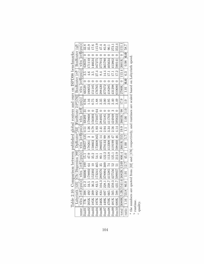
Tab
le2.
10:
Com
par
ison
bet
wee
npublish
edgl
obal
route
rsan
dou
rson
ISP
D98
ben
chm
arks.
Lab
yri
nth
[125
]C
hi
Dis
per
sion
[89]
DpR
oute
ra[3
2]Fas
tRou
te2.
0a[1
76]
Box
Rou
ter
(rtb )
Box
Rou
ter
(qlc )
nam
ew
len
ovfl
cpu(s
)w
len
ovfl
cpu(s
)w
len
ovfl
cpu(s
)w
len
ovfl
cpu(s
)w
len
ovfl
cpu(s
)w
len
ovfl
cpu(s
)ib
m01
77K
398
21.2
6600
618
915
.163
857
125
0.51
6848
931
0.94
6652
90
3.5
6265
90
32.8
ibm
0220
5K49
234
.517
8892
6447
.917
8261
31.
2617
8868
01.
1618
0053
04.
617
1110
035
.9ib
m03
185K
209
36.3
1523
9210
35.2
1506
630
0.78
1503
930
0.75
1511
850
3.5
1466
340
17.6
ibm
0419
7K88
283
.517
3241
465
54.1
1726
0816
51.
9317
5037
641.
8817
6765
027
.416
7275
011
5.9
ibm
0634
6K83
410
4.3
2892
7635
80.1
2860
2514
2.41
2849
350
2.35
2884
200
8.4
2779
130
47.4
ibm
0744
9K69
722
8.1
3789
9430
912
2.2
3791
3399
2.94
3751
850
2.00
3770
720
14.4
3657
900
85.9
ibm
0847
0K66
523
8.7
4152
8574
113.
841
2308
563.
3441
1703
02.
9541
8285
017
.140
5634
090
.1ib
m09
481K
505
359.
342
7556
5212
5.1
4191
9947
2.56
4249
493
2.40
4312
980
17.1
4138
620
273.
1ib
m10
680K
588
435.
759
9937
5121
2.9
5984
6046
4.14
5956
220
3.49
6106
800
17.2
5901
410
352.
4
tota
l30
89K
5.2K
1541
.626
82K
1249
806.
426
61K
555
19.9
2665
K98
17.9
2700
K0
113.
426
01K
011
51.1
rati
o1.
1653
.886
.01.
0112
.745
.01.
005.
71.
11.
001.
01.
01.
010.0
6.3
0.98
0.0
58.7
ath
enum
ber
sar
equot
edfr
om[3
2]an
d[1
76]re
spec
tive
ly,an
dru
nti
mes
are
scal
edbas
edon
Lab
yri
nth
spee
d.
bru
nti
me.
cqual
ity.
104

DpRouter, BoxRouter is 4-12x faster than the others. But, better congestion
distribution (no overflow) than FastRoute 2.0 and DpRouter will be signif-
icantly rewarded in detailed routing by huge speed-up. Therefore, a higher
quality solution should be preferred to runtime in global routing, unless the
main purpose of global router is the integration with placement [175]. When
tuned for quality, BoxRouter achieves the best wirelength, especially at least
9.7% better for ibm03.
2.3.5.3 New ISPD98 Benchmarks
As shown in Table 2.10, BoxRouter conquers ISPD98 benchmarks.
Therefore, ISPD98 benchmarks are not enough to push the limit of BoxRouter.
New ISPD07 routing benchmarks in Table 2.7 are too time/memory-consuming
to perform in-depth study of global routers and to provide insight on algorithm
in reasonable turn-around time. Therefore, we choose to reduce the capacities
of ISPD98 benchmarks (See Table 2.9) to test the limit of routing research,
and try BoxRouter on the new set of benchmarks. To avoid any confusion, we
name the two modified ISPD98 benchmarks as follows:
• ISPD98H(ard) Benchmarks: with less capacities than ISPD98 bench-
marks, and which can be marginally completed by BoxRouter.
• ISPD98I(mpossible) Benchmarks: with one fewer capacity than
ISPD98H benchmarks.
105

Table 2.11: BoxRouter results on ISPD98H/I benchmarks.ISPD98H ISPD98I
ver. hor. tot. BoxRouter ver. hor. tot. BoxRoutername cap cap cap wlen ovfl cpu(s) cap cap cap wlen ovfl cpu(s)ibm01 11 13 24 66554 0 122.3 10 13 23 70214 98 892.6ibm02 18 29 47 192827 0 995.0 17 29 46 201150 28 3.8Kibm03 17 27 44 160182 0 988.2 17 26 43 166083 58 3.1Kibm04 19 23 42 172104 0 386.9 19 22 41 173669 80 2.4Kibm05 24 44 68 439496 0 4.5K 23 44 67 460598 174 26.2Kibm06 16 29 45 308636 0 4.8K 16 28 44 323493 16 9.3Kibm07 18 32 50 392795 0 10K 17 32 49 410908 180 101.2Kibm08 17 28 45 439338 0 51K 17 27 44 447835 110 49.8Kibm09 11 25 36 461898 0 69K 11 24 35 505248 52 123.7Kibm10 20 32 52 728956 0 47K 19 32 51 771019 80 204.7K
total 171 282 453 3363K 0 190.3K 166 277 443 3530K 876 525.2Kratioa 0.78 0.85 0.82 1.03 0.00 345.2 0.76 0.83 0.80 1.08 0.015 912.7a capacities are normalized by original ISPD98 benchmarks in Table 2.9.
While reducing the capacity, we honor the original vertical/horizontal capacity
ratio by trying to reduce the same amount from both directions.
Table 2.11 reports the routing results of BoxRouter on ISPD98H and
ISPD98I benchmarks. Also, it reveals the reduced capacities of ISPD98H and
ISPD98I benchmarks. One can compare them with the original ISPD98 bench-
marks in Table 2.9. For this experiment, we simply use the default parameters
for BoxRouter for all the circuits. It shows BoxRouter can complete all the
circuits in ISPD98H benchmarks which have on average 18% fewer total ca-
pacity than original ISPD98 benchmarks. Even for ISPD98I benchmarks, it
creates at most 220 overflows for every circuit, which is even better than the
results of Chi Dispersion router on ISPD98 benchmarks in Table 2.10.
106

0 5 10 15 202.8
2.9
3
3.1
3.2
3.3
3.4x 10
5
Wir
elen
gth
Total capacity reduction0 5 10 15 20
0
0.5
1
1.5
2
2.5
3x 10
4
Ru
nti
me
RuntimeWirelength
(a) ibm02
0 5 10 15 20 25 30
6
7
8x 10
5
Wir
elen
gth
Total capacity reduction0 5 10 15 20 25 30
0
0.5
1
1.5
2x 10
5
Ru
nti
me
RuntimeWirelength
(b) ibm10
Figure 2.47: Runtime exponentially depends on total routing capacity, whilewirelength shows quadratic dependency.
Routing the harder cases involves significant runtime and wirelength
overhead as also shown in Table 2.11. We examine how runtime increases
with fewer capacities (difficulty of a circuit) for ibm02 and ibm10 where the
most amount of capacity reduction is achieved. Fig. 2.47 shows that the run-
time is exponentially dependent on the total capacity. This has an important
message to global routing in real practice. If routing capacity estimation con-
sidering prerouted nets as well as blockage porosity, is too conservative (much
fewer capacity than the actual capacity), it may incur significant and unnec-
essary runtime overhead. Of course, the other way incurs runtime overhead at
detailed routing stage.
Fig. 2.48 illustrates how strong BoxRouter is in terms of routability. In
spite of the reduced capacity, BoxRouter completes ibm01 by strongly pushing
the wires away from the congestion hotspots.
107

10 20 30 40 50 60
10
20
30
40
50
60
0
0.2
0.4
0.6
0.8
1
(a) ibm01 in ISPD98 benchmarks
10 20 30 40 50 60
10
20
30
40
50
60
0
0.2
0.4
0.6
0.8
1
(b) ibm01 in ISPD98H benchmarks
Figure 2.48: Although ibm01 in ISPD98H benchmarks has less capacity thanibm01 in ISPD98, ours achieves zero-overflowed solution by strongly spreadingout wires to less congested regions.
2.4 Summary
We develop various physical synthesis algorithms including floorplan-
ning [52], clock synthesis [50], and global routing [55, 56] to improve design
closure. Especially, our global router, BoxRouter pushed the state-of-the-art
considerably based on several innovative techniques including a new integer
linear programming (ILP) formulation.
First, in order to cope with significant substrate noise impact on analog
circuits from digital circuits, we propose substrate noise aware floorplanning
with fast substrate noise estimation powered by Block Preference Directed
Graph (BPDG) along with Sequence-Pair and B*-Tree. Compared with Par-
quet [1], the proposed approach has on average only 9% cpu time overhead,
whereas a naive model-based simulation approach shows over 6000% overhead.
Since BPDG is a general concept for fast cost evaluation, it will be extend to
108

deal with temperature or performance estimation in the future.
Next, in order to cope with the increasing impact of thermal variation,
we present an efficient, linear time temperature aware clock tree optimization
(TACO) algorithm to perform post-optimization. Experimental results show
that our approach reduces the worst case clock skew under thermal variation
significantly (up to 70%) with negligible increase (less than 0.6%) in the to-
tal wirelength. We plan to take the clock buffers and IR-drop with thermal
variation into account in the future.
Last, modern VLSI design becomes more complex and denser due to the
demand for high performance and various functionalities, making routability
even more challenging. In order to cope with routability issue, a key to suc-
cessful design closure, we propose a new global router, BoxRouter which can
effectively eliminate congestion. Experiments demonstrate the performance of
BoxRouter in terms of routability and wirelength/via on ISPD07 and ISPD98
benchmarks.
109

Chapter 3
Physical Synthesis for Manufacturing Closure
Nanometer VLSI design is facing increasing challenges from manufac-
turing limitations. These manufacturing/process challenges include printabil-
ity issues due to deep subwavelength lithography, topography variations due to
chemical-mechanical polishing (CMP), random defects due to missing/extra
material, and so on. Thus, for nanometer designs, design “closure” may not
have manufacturing closure owing to the yield loss, and physical synthesis for
manufacturing closure shall play a key role in the overall yield improvement.
Traditionally, we relied on the rules which have bridged design and
technology in order to continue the historical yield norm, as such rule-based
approach is friendly to a conventional design flow, which makes it seemingly
easy to implement and apply [152]. However, there can be several problems
with the rule-based approach in sub 90nm regime.
1. The number of rules is increasing exponentially with each new technology
node. For example, while the number of rules is only a few dozen at
180nm node, it reaches to several hundred at 65nm node. Even worse, a
single design rule may work differently depending on the design context.
110

(a) (b)
Figure 3.1: Context dependent minimum spacing rule for 65nm technology isshown [66]. Both cases, (a) and (b) are described in the table.
2. The complexity of checking such rules becomes more computationally
expensive, as the rules are increasingly context-sensitive [66,69,140]. For
example, the minimum spacing between wires may depend on the wire
lengths and the neighborhood wires, as shown in an example in Fig. 3.1.
Therefore, simply checking rules by itself needs considerable amount of
computing resource.
3. The rules are binary in nature, i.e., either following a rule or violating
a rule. Thus the rule-based approach does not provide smooth trade-off
among various design objectives such as timing, power, noise, and so on.
111
4. The rules themselves may be too restrictive and pessimistic, leaving too
much power or performance on the table. In some cases, it may be
infeasible to achieve the performance goals due to over guard-band from
the rules. Furthermore, the rules may not be accurate enough to model
very complicated manufacturing processes, in particular for the future
deeper subwavelength lithography systems.
Due to these limitations of the conventional rules, there have been sig-
nificant ongoing efforts in manufacturing closure with manufacturing models in
both academia and industry, expecting that models will capture manufacturing
effects more accurately at affordable computational overhead coupled with a
small number of simple design rules. And, it is known that routing in physical
synthesis is the right stage to incorporate such models for enhanced manufac-
turing closure, which strongly motivates manufacturability aware routing.
In this chapter, we present three routing algorithms to optimize topog-
raphy variation after CMP, random defects due to missing/extra material, and
printability degradation due to subwavelength lithography. We will begin with
the motivation for manufacturability optimization during routing and describe
our routing framework to enhance manufacturing closure in physical synthesis
in Section 3.1.
In Section 3.2, we propose the first wire density-driven global routing
that considers CMP variation and timing. To enable CMP awareness during
global routing, we propose a compact predictive CMP model with dummy fill,
112
and validate it with extensive industry data. While wire density has some
correlation and similarity to a conventional congestion metric, they are indeed
different in the global routing context. Therefore, wire density rather than
congestion should be a unified metric to improve both CMP variation and
timing. The proposed wire density-driven global router is implemented in a
routability-driven BoxRouter [51] for CMP and timing optimization. The new
global router utilizes several novel techniques to reduce the wire density of
CMP and timing hotspots. Our experimental results are very encouraging.
The proposed algorithm improves CMP variation and timing by over 7% with
negligible overhead in wirelength and even slightly better routability, compared
to the pure BoxRouter [51].
In Section 3.3, we propose TROY, the first track router for the opti-
mization of yield loss due to random defects. As the probability of failure
(POF) which is an integral of critical area under a defect size distribution,
strongly depends on wire ordering, sizing, and spacing, track routing can
play a key role in effective wire planning for yield optimization. However,
a straightforward formulation of yield-driven track routing can be shown to be
integer nonlinear programming which is a NP-complete problem. TROY over-
comes the computational complexity by combining two effective techniques,
i.e., minimum Hamiltonian path from graph theory and second order cone pro-
gramming (SOCP) from mathematical optimization. First, TROY performs
wire ordering to minimize critical area for short defects by finding a mini-
mum Hamiltonian path. Then, TROY carries out optimal wire sizing/spacing
113

through SOCP optimization based on a given wire order. Since SOCP can
be solved optimally in near linear time, TROY achieves globally optimal wire
sizing/spacing efficiently for the minimal POF. Experimental results on IBM
benchmarks show that TROY can reduce the random-defect induced yield
loss by 18% on average without any overhead in wirelength, compared with a
widely used greedy approach.
In Section 3.4, we present ELIAD, an efficient lithography aware de-
tailed router to optimize silicon image after Optical Proximity Correction
(OPC) in a correct-by-construction manner. We first quantitatively show that
pre-OPC and post-OPC litho-metrics are highly uncorrelated, which stresses
the importance of a post-OPC litho-metric for design time optimization. We
then propose a compact post-OPC litho-metric for a detailed router based
on statistical characterization. We characterize the interferences among weak
grids filled with one of predefined litho-prone shapes (e.g., jog-corner, via, line-
end). Our litho-metric derived from such characterization shows high fidelity
to total edge placement error (EPE) in large scale, compared with Calibre-
OPC/ORC. As a chip itself is in the largest scale, ELIAD powered by the
proposed metric can enhance the overall post-OPC printed silicon image. Ex-
perimental results on 65nm industrial circuits show that ELIAD outperforms a
ripup/rerouting approach such as RADAR [154] with 8x more EPE hotspot re-
duction and 12x speedup. Also, compared with a conventional detailed router,
ELIAD is only about 50% slower.
114
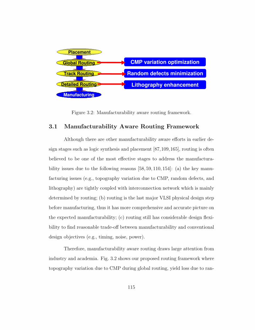
CMP variation optimization
Random defects minimization
Lithography enhancement
Global Routing
Track Routing
Detailed Routing
Global Routing
Track Routing
Detailed Routing
Placement
ManufacturingManufacturing
Figure 3.2: Manufacturability aware routing framework.
3.1 Manufacturability Aware Routing Framework
Although there are other manufacturability aware efforts in earlier de-
sign stages such as logic synthesis and placement [87,109,165], routing is often
believed to be one of the most effective stages to address the manufactura-
bility issues due to the following reasons [58, 59, 110, 154]: (a) the key manu-
facturing issues (e.g., topography variation due to CMP, random defects, and
lithography) are tightly coupled with interconnection network which is mainly
determined by routing; (b) routing is the last major VLSI physical design step
before manufacturing, thus it has more comprehensive and accurate picture on
the expected manufacturability; (c) routing still has considerable design flexi-
bility to find reasonable trade-off between manufacturability and conventional
design objectives (e.g., timing, noise, power).
Therefore, manufacturability aware routing draws large attention from
industry and academia. Fig. 3.2 shows our proposed routing framework where
topography variation due to CMP during global routing, yield loss due to ran-
115

dom defects during track routing, and printability degradation due to subwave-
length lithography during detailed routing are addressed respectively. This
framework optimizes multiple key manufacturability issues at different rout-
ing steps according to the granularity of routing algorithms and the availability
of inputs to models. For example, it might be impossible to enhance print-
ability during global routing due to the lack of inputs to a lithography model,
while reducing CMP variation during detailed routing may not be effective
enough due to the localized optimization scope of detailed routing.
3.2 Global Routing for CMP and Timing optimization
Manufacturability and yield are becoming ever-serious concerns at 90nm
node and below, and shown to be heavily affected by design patterns [184]. Es-
pecially, topography (thickness) variation after chemical-mechanical polishing
(CMP) due to copper dishing/erosion is shown to be systematically deter-
mined by wire density distribution [135,184,244]. Even after CMP, intra-chip
topography variation can still be on the order of 20-40% [91, 184]. Such to-
pography variation leads to not only significant performance degradation due
to increased wire resistance and capacitances, but also acute manufacturing
issues like etching and printability [81,91,184,205].
The main key to the above problems is in wire density distribution.
Higher wire density usually leads to copper thickness reduction due to ero-
sion after CMP [135,244], making resistance worse. Also, the reduced copper
thickness after CMP can worsen the scattering effect, further increasing re-
116

sistance [116]. Meanwhile, a region with higher wire density tends to have
less spacing between wires, thus significantly increasing coupling capacitance
between them. For a lower wire density region, dummy fill is performed before
CMP to make density distribution more uniform, expecting less topography
variation after CMP. However, dummy fill is usually applied in a post-design
stage, and has limitations due to strict rules (such as fill size, patten, spacing
to other features) which intend to minimize the disturbance in the existing
design. Thus, non-uniform distribution of density still exists even after the
dummy fill, creating topography variation which wastes the minuscule depth
of focus regarding printability [75].
The global routing, as its name implies, is the routing stage that plans
the approximate routing path of each net to reduce the complexity of routing
task and guide the detailed router [107]. Thus, it has significant impact on
wirelength, congestion/routability and wire density distribution, hence CMP
variation and timing [81, 106,107,222]. The global routing should be an ideal
stage for the first order to improve CMP variation as well as timing by optimiz-
ing wire density distribution [19,227]. Even though there have been significant
amount of work in global routing about crosstalk [19,94,125,127,193,214,246],
timing [19,106,227,234] and congestion/routability [5,51,89], none of them has
worked on the optimization of wire density distribution for CMP variation and
timing.
In this section, we propose a new paradigm of wire density-driven global
routing to improve CMP variation and timing. To our best knowledge, this
117

is the first work that takes wire density distribution into account to enhance
both CMP variation and timing, while considering congestion and wirelength.
Essentially, the proposed algorithm minimizes the wire density around timing
critical nets to enhance timing, and the wire density of dense global routing
cells to reduce topography variation after CMP. The major contributions of
this section include the following.
• We present a simple predictive CMP model verified with industrial cases
for the first time. We also show that only few regions of a chip are
responsible for most of topography variation after CMP. This means
that selective optimization of wire density distribution can enhance the
uniformity of topography.
• We use the wire density to guide global routing for CMP variation and
timing. We show that wire density and congestion are not linearly pro-
portional to each other. This implies that just congestion-driven global
routing cannot address the wire density issue efficiently. Furthermore,
we observe that wire delay is near linearly proportional to wire density
in global routing even with CMP effect (dishing/erosion and dummy
fill) [91,139,244] and scattering effect [116] taken into consideration.
• We propose several novel wire density-driven routing techniques for CMP
variation and timing optimizations, including minimum pin density rout-
ing, timing sensitivity map, and CMP aware wire density distribution.
118
Each technique helps global routing reduce the wire density around tim-
ing critical nets, while minimizing topography variation after CMP.
Our approach achieves better timing and less topography variation
than the state-of-the-art academic routability-driven router, BoxRouter in
Section 2.3 with negligible overhead on wirelength, and even better conges-
tion/routability.
The rest of the section is organized as follows. A predictive CMP model
is presented, and timing impact with wire density distribution is analyzed in
Section 3.2.1. In Section 3.2.2, a wire density-driven global routing is proposed.
Experimental results are discussed in Section 3.2.3.
3.2.1 Predictive CMP Model and Timing Impact
In this section, we propose a predictive CMP model for the first time.
It is followed by the study of the timing impact of wire density under CMP
(topography variation and dummy fill) [81] and scattering effect [116]. Then,
we show that congestion-driven routing cannot replace wire density-driven
routing .
3.2.1.1 Wire Density and Predictive CMP Model
Topography variation (thickness variation) after CMP is determined by
underlying metal density which includes both wires and dummies. As dummy
fill in turn depends on wire density, the required dummy density and the
copper (Cu) thickness can be predicted from a given wire density.
119
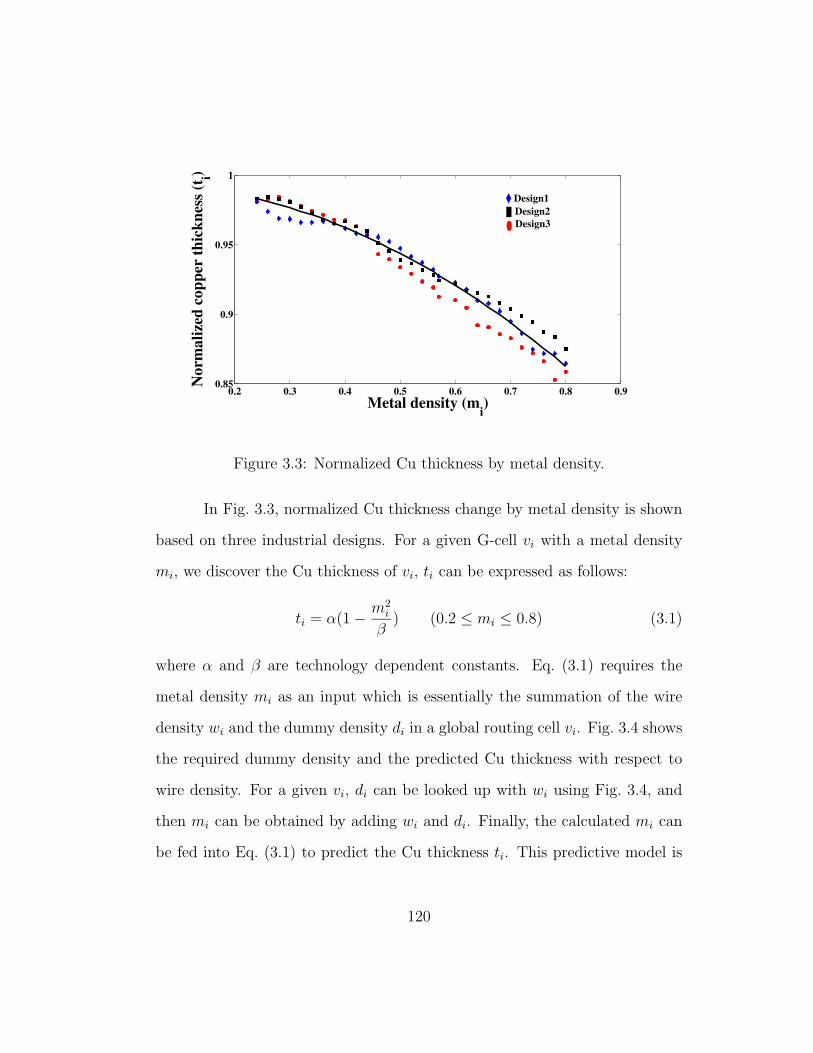
0.2 0.3 0.4 0.5 0.6 0.7 0.8 0.90.85
0.9
0.95
1
Norm
ali
zed
cop
per
th
ick
nes
s (t
i)
Metal density (mi)
Design1
Design2
Design3
Figure 3.3: Normalized Cu thickness by metal density.
In Fig. 3.3, normalized Cu thickness change by metal density is shown
based on three industrial designs. For a given G-cell vi with a metal density
mi, we discover the Cu thickness of vi, ti can be expressed as follows:
ti = α(1 −m2
i
β) (0.2 ≤ mi ≤ 0.8) (3.1)
where α and β are technology dependent constants. Eq. (3.1) requires the
metal density mi as an input which is essentially the summation of the wire
density wi and the dummy density di in a global routing cell vi. Fig. 3.4 shows
the required dummy density and the predicted Cu thickness with respect to
wire density. For a given vi, di can be looked up with wi using Fig. 3.4, and
then mi can be obtained by adding wi and di. Finally, the calculated mi can
be fed into Eq. (3.1) to predict the Cu thickness ti. This predictive model is
120

0.1 0.2 0.3 0.4 0.5 0.6 0.7 0.8 0.90
0.2
0.4
0.6
0.8
1
Du
mm
y /
Met
al
den
sity
(d
i/mi)
Wire density (wi)
0.1 0.2 0.3 0.4 0.5 0.6 0.7 0.8 0.90.75
0.8
0.85
0.9
0.95
1
Norm
ali
zed
cop
per
th
ick
nes
s (t
i)
Normalized copper thickness (ti)
Metal (Wire+Dummy) density (mi)
Dummy density (di)
Figure 3.4: Predictive CMP model.
verified with a commercial CMP simulator [105] and industry test cases. Our
predictive CMP model can be used for placement due to its compactness [46].
3.2.1.2 Wire Density and Timing
For two adjacent wires, each has two capacitance components, coupling
capacitance Cc between itself and the other wire, and ground capacitance Cg
between itself and ground. Bakoglu [14] shows that wire delay on a distributed
RC network contains the following delay component, D:
D ∝ (Rd + r · l)(Cg + Cc) = (Rd +ρ · l
w · t)(
ǫ · l · w
h+
ǫ · l · t
s) (3.2)
where Rd is the driver resistance, ρ is the resistivity of the wire, ǫ is the
insulator dielectric constant, w, t ,and h are the wire width, thickness, and
distance from the substrate, respectively. And, l and s are the length and
121

spacing between two coupled wires, respectively.
In Eq. (3.2), h is a constant, and w can be assumed to be a constant
as well (we do not consider the width variation effect in this subsection as
it is relatively small for Cu process). Without loss of generality, we just use
the nominal wire width. For a given G-cell vi, ti is essentially a function of
wi (mi depends on wi as in Fig. 3.4), and can be denoted as ti(wi). If even
spacing between wires and square G-cell are assumed, spacing between wires
si becomes a function of wi:
si(wi) = li ·1 − wi
ni + pi
∝1
wi
− 1 (0 < wi ≤ 1) (3.3)
Also, we can obtain the increased total capacitance due to dummy fill
(dummy increases coupling capacitance) as a function of wi based on [139]:
f(wi) = 1 + γ log(si(wi)
δ) (3.4)
where γ and δ are technology dependent constants. Note that f(wi) is
typically less than 1.1, and saturates quickly. Due to scattering effect under a
given temperature, ρ is a function of ti. Thus, it is also a function of wi (see
Eq. (3.1)), and can be denoted as ρ(wi) [116]. Finally, the component of the
wire delay in vi can be rewritten as a function of wi based on Eq. (3.2):
R(wi) =ρ(wi) · li
ti(wi) · Wnom
(3.5)
C(wi) = ǫ · f(wi)(li · Wnom
h+
li · ti(wi)
si(wi)) (3.6)
122

D(wi) ∝ (Rd + R(wi))C(wi) ∝ wi (3.7)
We observe the following with sub 65nm technology node:
• Lower wire density shows less resistance (less erosion after CMP) as well
as less capacitance (more spacing between wires).
• Resistance variation dependence on wire density (computed after post
dummy fill and CMP estimation) is relatively smaller than capacitance
variation.
• D(wi) is near linearly proportional to wi in the region where most of
wire densities exist (see Eq. (3.3) and (3.6)).
3.2.1.3 Wire Density and Congestion
While congestion/routability has been the main concern in global rout-
ing, wire density distribution is an emerging important objective due to CMP
variation and timing as shown in Section 3.2.1.1 and 3.2.1.2. Although wire
density is closely related to congestion, congestion-driven global routing can-
not address wire density issues directly and effectively, because wire density is
computed for the wires inside a global routing cell, while congestion is com-
puted for the wires crossing the edges of a global routing cell.
Fig. 3.5 shows a G-cell with edge A and B which have seven routing
resources. Fig. 3.5 (a) and (b) show that the density is a half of the congestion
(gA and gB). However, when there is a wide wire such as power/ground as
123
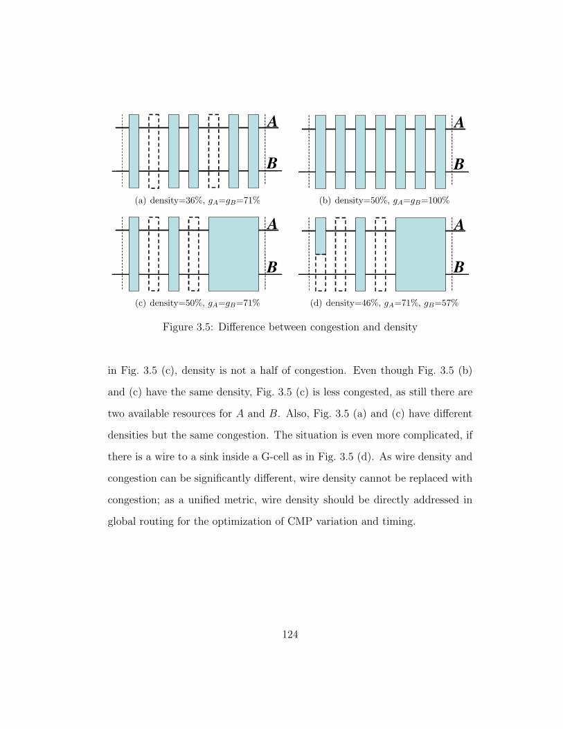
A
B
(a) density=36%, gA=gB=71%
A
B
(b) density=50%, gA=gB=100%
A
B
(c) density=50%, gA=gB=71%
A
B
(d) density=46%, gA=71%, gB=57%
Figure 3.5: Difference between congestion and density
in Fig. 3.5 (c), density is not a half of congestion. Even though Fig. 3.5 (b)
and (c) have the same density, Fig. 3.5 (c) is less congested, as still there are
two available resources for A and B. Also, Fig. 3.5 (a) and (c) have different
densities but the same congestion. The situation is even more complicated, if
there is a wire to a sink inside a G-cell as in Fig. 3.5 (d). As wire density and
congestion can be significantly different, wire density cannot be replaced with
congestion; as a unified metric, wire density should be directly addressed in
global routing for the optimization of CMP variation and timing.
124

3.2.2 Wire Density Driven Global Routing for CMP and Timing
In this subsection, we propose our wire density-driven global routing
algorithm which essentially minimizes the delay of timing critical nets by de-
creasing the wire density around such nets, and improves the topography varia-
tion after CMP by decreasing the wire density of dense G-cells selectively. Our
approach consists of four ideas which can be easily integrated with any existing
global router [5, 51, 89, 125]; minimum pin density routing in Section 3.2.2.1,
timing sensitivity map in Section 3.2.2.2, selective wire density optimization
for CMP awareness in Section 3.2.2.3, and wire density-driven maze routing
in Section 3.2.2.4.
3.2.2.1 Minimum Pin Density Routing
In practice, timing critical nets are commonly routed before other nets
for the minimum length. As there can be multiple paths with the minimum
length, a router can choose any of these based on its policy. However, we find
that a path with the minimum pin density is better for the wire density distri-
bution. In Fig. 3.6, a net D-S to be routed is shown with a pin distribution. If
only L-shape routing is allowed, we can have two possible paths, a and b with
the same length but different pin densities. As the existence of a pin means a
connection to other pins, a path with higher pin density like b tends to have
higher wire density eventually as in Fig. 3.6 (b), resulting in higher resistance
and larger coupling capacitance.
More importantly, the path with higher pin density cannot get much
125

D
Sa
b
(a) two possible paths forD-S
D
Sa
b
(b) path b with higher density
Figure 3.6: Example of minimum pin density routing.
benefit from the wire density optimization, as there is little room for improve-
ment (it is destined to have high wire density from the beginning). Note
only L/Z-shape routing is considered in the minimum pin density routing to
minimize the number of vias in our implementation.
3.2.2.2 Timing Sensitivity Map Construction
As Elmore delay can be expressed as the summation of RC products
where C is the downstream capacitance seen by R in a distributed RC network,
capacitance close to the sink has more impact on timing than one close to the
driver. Also, the capacitance of a G-cell where more timing critical nets are
passing has more impact on timing. Thus, we can compute the sensitivity of
each G-cell to timing, and construct a timing sensitivity map. As resistance is
relatively insensitive to wire density variation (see Section 3.2.1.2), we consider
126
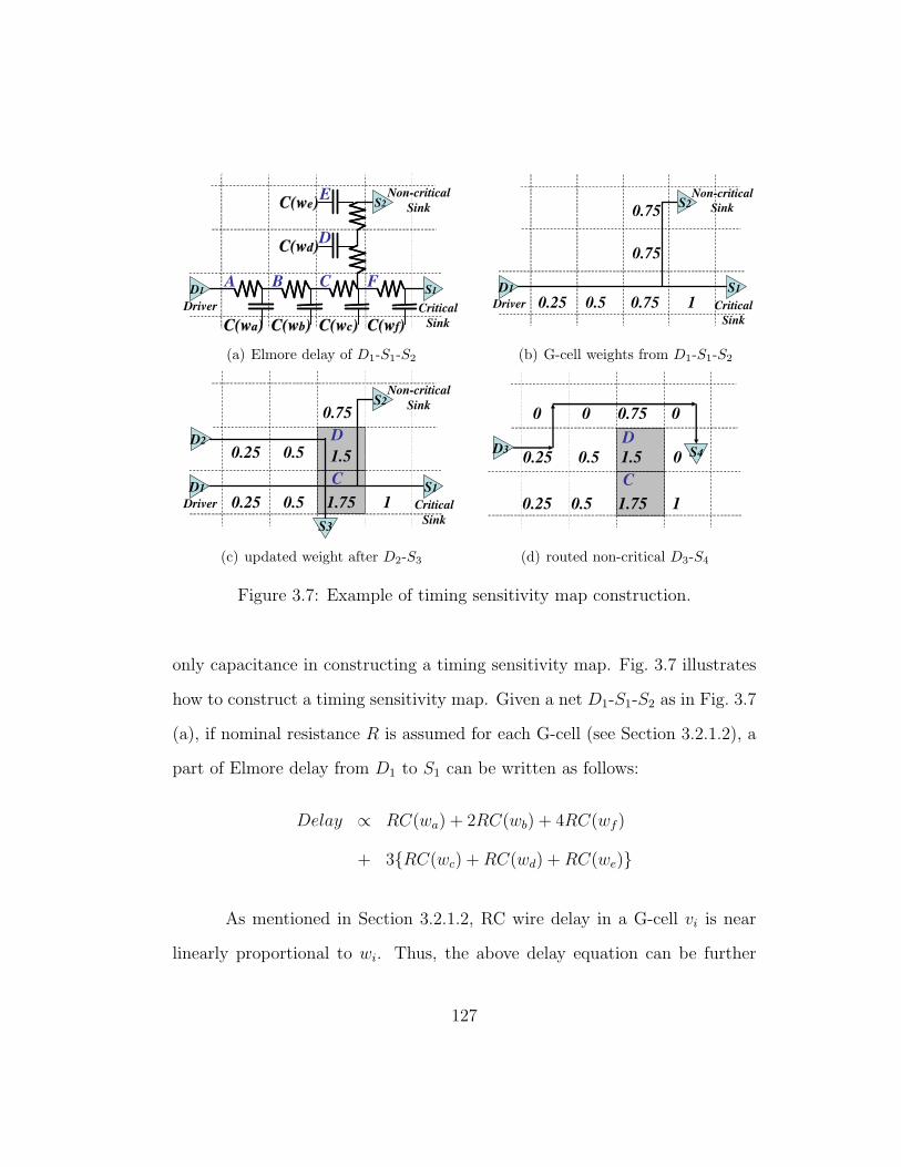
D1
C(wC(waa))
Driver
S1
Critical
Sink
Non-critical
SinkS2
D
A B C
E
F
C(wC(wbb)) C(wC(wcc)) C(wC(wff))
C(wC(wdd))
C(wC(wee))
(a) Elmore delay of D1-S1-S2
D1
Driver
S1
Non-critical
SinkS2
0.25 0.5 0.75 1
0.75
0.75
Critical
Sink
(b) G-cell weights from D1-S1-S2
D1
Driver
S1
Critical
Sink
Non-critical
SinkS2
0.25 0.5 1.75 1
0.75
D2
S3
0.25 0.5 1.5
D
C
(c) updated weight after D2-S3
D3
0.25 0.5 1.75 1
0.75
0.5
0
1.5 S4
0
0.25
0
D
C
0
(d) routed non-critical D3-S4
Figure 3.7: Example of timing sensitivity map construction.
only capacitance in constructing a timing sensitivity map. Fig. 3.7 illustrates
how to construct a timing sensitivity map. Given a net D1-S1-S2 as in Fig. 3.7
(a), if nominal resistance R is assumed for each G-cell (see Section 3.2.1.2), a
part of Elmore delay from D1 to S1 can be written as follows:
Delay ∝ RC(wa) + 2RC(wb) + 4RC(wf )
+ 3RC(wc) + RC(wd) + RC(we)
As mentioned in Section 3.2.1.2, RC wire delay in a G-cell vi is near
linearly proportional to wi. Thus, the above delay equation can be further
127

Algorithm 9 Timing Sensitivity Map Construction
Input: List of timing critical nets and G-cells1: tsi = 0 ∀ G-cell i2: for each timing critical net N do3: P = Path from critical sink S to driver D4: Ls = Path length from S to D5: for each G-cell vj ∈ P do6: Lj = Path length from vj to D7: tsj = tsj+Lj/Ls
8: end for9: for each G-cell vj /∈ P,∈ N do
10: vx = G-cell closest to vx ∈ P11: Lx = Path length from vx to D12: tsj = tsj+Lx/Ls
13: end for14: end forOutput: Timing sensitivity map
simplified as follows:
Delay ∝ wa + 2wb + 4wf + 3wc + wd + we
It is clear that each wire segment (thus, each G-cell) has different impact
on the timing due to its geometrical location (whether it is close to driver or
not). For example, 10% increase of wf has the same impact as 40% increase of
wa on timing. Therefore, each G-cell can have its own time sensitivity to the
density change as in Fig. 3.7 (b). We can apply the same idea to all the timing
critical nets which are already routed by the minimum pin density routing, and
sum up the timing sensitivity from each net to construct a timing sensitivity
map. For example, in Fig. 3.7 (c), another timing critical net D2-S3 is joining
the net D1-S1-S2 at the G-cell vC and vD. As vC has already 0.75 as the timing
128

0.82 0.84 0.86 0.88 0.9 0.92 0.94 0.96 0.98 10
0.02
0.04
0.06
0.08
0.1
0.12
0.14
0.16
Norm
ali
zed
nu
mb
er o
f G
−ce
lls
Normalized copper thickness
Figure 3.8: Normalized Cu thickness distributions of four industrial designs.
sensitivity tsC , after considering D2-S3, tsC becomes 1.75 due to 1 from D2-S3.
In the same manner, tsD becomes 1.5 due to another 0.75 from D2-S3. With
the timing sensitivity of each G-cell, we can make a non-timing critical net
D3-S4 detour to reduce the wire density of the highly timing sensitive G-cell
like vD as in Fig. 3.7 (d). This improves the overall timing by reducing the
wire density of more timing sensitive G-cells, while minimizing the overhead
in wirelength. Algorithm 9 shows how to construct the timing sensitivity map.
3.2.2.3 CMP Aware Wire Density Distribution
To improve CMP variation, more uniform metal density distribution
should be achieved by increasing density for less dense G-cells or decreasing
density for more dense G-cells. We find that reducing wire density of the more
129

Algorithm 10 Wire Density Driven Maze Routing
Input: G-cell vi and Parameter P,Q, Td
1: Cost C = Costo //from other optimization costs2: if tsi > 0 then3: C += P · wi · (1 + tsi) //timing sensitivity4: else if mi > Td then5: C += Q · wi //CMP awareness6: end if
Output: C
dense G-cells can be more effective than the other way for two reasons. First,
it requires to perturb a smaller number of G-cells. Fig. 3.8 shows Cu thickness
distributions of four industrial cases after CMP. It shows only few G-cells have
over 5% of Cu loss, and are mainly responsible for topography variation. Thus,
optimizing G-cells over a threshold metal density Td can make topography
more uniform without disturbing other design objectives. Second, lowering
wire density also helps congestion, despite that they are weakly correlated.
3.2.2.4 Wire Density Driven Maze Routing
Wire density distribution governs both CMP variation and timing. The
objective for timing requires lower density for the timing sensitive G-cell, and
the objective for CMP variation requires lower density for the G-cells above
the threshold of Section 3.2.2.3. Wire density-driven maze routing is shown
in Algorithm 10. Note that mi can be computed from the CMP model in
Section 3.2.1.1, and Costo is for other design objectives such as congestion.
Two parameters, P and Q are introduced to control the trade-off between
objectives.
130

3.2.3 Experimental Results
We implement our proposed algorithm by modifying BoxRouter in Sec-
tion 2.3, and compare the results with the original BoxRouter. All the exper-
iments are performed on a 2.8 GHz Pentinum-4 Linux machine. The ISPD98
IBM benchmarks are taken from [101], and we modify the horizontal and ver-
tical capacity of each circuit as shown in Table 3.1. Further, assuming up to
30% of routing capacity is assigned for wide wires like power/ground, we reduce
the routing capacity to get a enough number of overflows (to see the impact
on congestion/routability), and make the horizontal and the vertical capacity
same for easy wire density calculation. Since the original benchmarks do not
have any timing information, we randomly pick less than 1% nets which are
longer than 200µm as optimization targets. HSPICE simulation with 65nm
technology is performed to estimate timing with CMP variation and scatter-
ing effect taken into account. All the timing critical nets are pre-routed in the
same minimum length and same topology in any experiment to eliminate the
effect of different path lengths and topologies on timing.
Fig. 3.9 (a) shows total/max delay and wirelength change by the pa-
rameter P with Q=0. While the wirelength increases as P increases, the delay
decreases until P=1, and then starts increasing after that. The reason is be-
cause too much increase in wirelength due to detouring around timing sensitive
G-cells (with higher P value), finally makes overall congestion worse. This pro-
vokes the congestion-driven objective to push wires back to the timing sensitive
G-cells. All the following simulations use P=1, as it shows reasonable trade-
131

0 1 2 3 4 5 6 7 8 9 10
−10
−5
0
5
Del
ay
an
d
wir
elen
gth
ch
an
ge
(%)
P
WirelengthTotal DelayMax Delay
(a) P with Q=0
0.5 1 1.5 2
−10
−8
−6
−4
−2
0
Del
ay
, w
irel
eng
th a
nd
top
og
rap
hy
va
r. c
ha
ng
e(%
)
Q
Total delayMax delay
Wirelength
Topography variation
(b) Q with P=1
Figure 3.9: Effectiveness of parameter P and Q.
off. Fig. 3.9 (b) shows total/max delay, wirelength, and topography variation
change by the parameter Q with P=1. While the total delay and max delay
increase with larger Q, the topography variation decreases. Wirelength does
not change noticeably, proving that our selective wire density optimization for
CMP variation is friendly with other design objectives. Although the topog-
raphy variation can be improved by over 10% with large Q, all the following
simulations use Q=1.3 for the minimal impact on timing.
Table 3.1 shows the experimental results and comparison of the pro-
posed algorithm (the modified BoxRouter) with the original BoxRouter. The
experiment sets P=1, Q=1.3, and Td=0.33 of Algorithm 10 to evaluate the
optimization for CMP variation and timing together. The average of total
delay and max delay are slightly reduced to 7.0% and 8.0% respectively, while
topography variation after CMP is improved by 7.5% on average and up to
10.1%. The overhead in CPU time is still only 41% on average. Also routabil-
132

Tab
le3.
1:C
ompar
ison
wit
hB
oxR
oute
rfo
rIS
PD
98ben
chm
arks.
circ
uit
Box
Rou
ter
Wir
eD
ensi
tyD
rive
nB
oxR
oute
rC
han
ge(%
)nam
ehz.
vt.
t.del
a m.d
elb
wle
nc
ovfl
d dum
et.
vf
cpu
t.del
m.d
elw
len
ovfl
dum
t.v
cpu
t.del
m.d
elw
len
ovfl
dum
t.v
cpu
cap
cap
(ns)
(ps)
(%)
(sec
)(n
s)(p
s)(%
)(s
ec)
ibm
0118
180.
5730
.161
374
437
21.
347.
10.
5426
.061
437
136
41.
258.
7-6
.4-1
3.4
0.1
-75.
0-2
.2-6
.722
.5ib
m02
3636
1.85
67.6
1808
1625
357
1.94
34.8
1.77
67.7
1788
2629
352
1.82
45.1
-4.5
0.1
-1.1
16.0
-1.4
-6.2
29.6
ibm
0331
311.
9175
.714
8530
538
91.
7316
.01.
7974
.114
9258
1038
41.
6524
.5-6
.4-2
.10.
510
0.0
-1.3
-4.6
53.1
ibm
0426
261.
6161
.416
7557
9944
11.
7520
.01.
4959
.516
7515
7943
11.
6327
.0-7
.6-3
.00.
0-2
0.2
-2.3
-6.9
35.0
ibm
0545
453.
7525
2.2
4265
4710
054
21.
7851
.13.
5022
3.8
4269
2961
534
1.66
83.1
-6.6
-11.
30.
1-3
9.0
-1.5
-6.7
62.6
ibm
0635
352.
1024
3.8
2838
3611
540
1.42
33.1
1.97
232.
728
4619
353
11.
3151
.5-6
.6-4
.60.
3-7
2.7
-1.7
-7.7
55.6
ibm
0734
341.
7710
0.7
3722
6818
867
1.67
46.5
1.65
92.9
3730
6810
847
1.56
66.0
-6.8
-7.8
0.2
-44.
4-2
.3-6
.641
.9ib
m08
3131
2.62
191.
842
0609
7277
01.
7294
.22.
4116
7.9
4188
2554
756
1.56
125.
5-7
.9-1
2.5
-0.4
-25.
0-1
.8-9
.333
.2ib
m09
2525
2.32
192.
843
2120
7510
911.
5968
.82.
1416
8.4
4324
8747
1061
1.43
90.9
-7.5
-12.
70.
1-3
7.3
-2.7
-10.
132
.1ib
m10
4343
3.21
799.
058
4100
3311
831.
4890
.52.
8969
4.9
5864
954
1131
1.33
129.
6-1
0.0
-13.
00.
4-8
7.9
-4.4
-10.
143
.2av
erag
e-7
.0-8
.00.
0-2
8.6
-2.2
-7.5
40.9
(a)
tota
ldel
ay(b
)m
axdel
ay(c
)w
irel
engt
h(d
)ov
erflow
(e)
the
amou
nt
ofdum
my
(f)
topog
raphy
vari
atio
naf
ter
dum
my
fill(s
td/a
vg)
133
ity is improved, as the number of G-cells with high wire density (which tend to
be congested) is reduced by CMP aware wire density distribution. As already
shown in Fig. 3.9 (b), wirelength overhead is quite small, and the improved
routability even suppresses the increase in wirelength (less detouring).
3.3 Track Routing for Random Defect Optimization
Smaller feature size makes nanometer VLSI designs more vulnerable to
ever-growing yield loss due to both random and systematic causes [130]. While
it is believed that the yield loss due to systematic sources is greater than that
due to random defects during the technology and process ramp-up stage, the
systematic yield loss can be largely eliminated when the process becomes ma-
ture, tuned, and systematic variations are extracted/compensated [150]. On
the other hand, the random defects which are inherent due to manufacturing
facility limitations will still exist for mature fabrication process [130]. Thus,
its relative importance will indeed be much bigger for mature process with
systematic variations designed in. Among random defects, the density of back-
end-of-line (BEOL) defects (i.e., interconnect defects) is increasing, compared
to that of front-end-of-line (FEOL) defects (i.e., device defects) [120]. Since
the random BEOL defects mainly occur either between physically adjacent
interconnects (short defects) or on interconnect itself (open defects), routing
and interconnect optimization should be the suitable place for random-defect
related yield optimization [27,130,177].
In general, routing consists of two steps, global routing and detailed
134

routing. Global routing plans an approximate path for each net, while detailed
routing finalizes the exact DRC-compatible pin-to-pin connections. Track
routing, as an intermediate step between global and detailed routing, can
expedite detailed routing by embedding major trunks from each net within a
panel (a row/column of global routing cells) in a DRC-friendly manner [17].
Such track routing is an appealing stage to optimize critical area for
yield enhancement, as decent flexibility in routing optimization exists with wire
adjacency information [68,130,229] which global routing is lack of, for accurate
critical area estimation. Meanwhile, detailed routing does not have sufficient
flexibility to make radical routing changes for yield enhancement. Therefore,
wire ordering to minimize the overlapped wirelength between adjacent wires
as well as wire sizing/spacing can be effectively performed in track routing to
make a design more robust to random defects.
Due to the criticality of yield in the semiconductor industry, there have
been considerable amount of efforts to enhance yield by reducing critical area in
routing or post-layout optimization. Wire ordering [133,181] and spacing [15,
27,49] to reduce the density of short defects are explored. Redundant link [120]
to improve immunity to open defects is studied. Wire spreading in the post-
routing optimization for yield is in [8,203]. However, there are a few drawbacks
in these prior works:
• One single defect size is considered, rather than a defect size distribu-
tion [133,181].
135
• The trade-off between open and short defects due to limited chip area is
ignored [8, 15,120,133,181].
• Localized/greedy optimization is performed, which may increase overall
critical area [15,27,49,120,203].
• Wire adjacency information is not available for accurate critical area
estimation [112,161].
Indeed, it is required to find the best trade-off between open and short defects
within a fixed routing area under a given defect size distribution through wire
planning (wire ordering, sizing, and spacing) in a global scope. Accordingly,
track routing is the right stage for such optimization.
So far, most recent track routing algorithms have focused on crosstalk
or timing optimization [17, 126, 208, 229], but none of them have discussed
yield optimization. At the first glance, crosstalk and critical optimizations
share some common traits as wire spacing helps both. However, the roles that
wire ordering, wire sizing, and wire spacing play on yield and crosstalk opti-
mizations are very different. For example: yield optimization has to consider
a defect size distribution and all adjacent wires, but crosstalk optimization
only needs to consider these adjacent wires with overlapping timing windows;
power and ground wires provide shielding against crosstalk, but there is no
such shielding counterpart for yield; and so on. Moreover, the algorithms
in [17,126,208,229] can neither perform wire planning in a global manner nor
consider the trade-off between random defects.
136

In this section, we propose TROY, the first track router with yield op-
timization based on wire planning (wire ordering, sizing, and spacing). TROY
first orders wires to minimize overlapped wirelength between adjacent wires
based on preference aware minimum Hamiltonian path, and then performs
globally optimal wire sizing and spacing for the ordered wires with efficient
second order cone programming (SOCP). As a result, globally optimal wire siz-
ing/spacing as well as minimal overlapped wirelength decreases critical area,
making a design more robust against random defects. The major contributions
of this section include the following.
• We propose TROY, a track router with yield optimization. To our best
knowledge, this is the first work that yield is optimized during track
routing.
• We propose a simple model of probability of failure due to random de-
fects. This simple, yet effective model enables highly efficient and scal-
able SOCP.
• We show that wire ordering within a panel (the first step of wire plan-
ning in TROY) can be efficiently solved by preference aware minimum
Hamiltonian path formulation. TROY considers the interaction between
adjacent panels to overcome any disadvantage from an isolated panel-by-
panel approach.
• We show that wire sizing and spacing for an entire layer (the second step
137
of TROY) can be formulated as SOCP which can be solved optimally
and as efficiently as linear programming.
The rest of the section is organized as follows. Section 3.3.1 presents
preliminaries. Section 3.3.2 shows a general formulation of yield-driven track
routing, and then proposes the TROY as an efficient algorithm. Experimental
results are discussed in Section 3.3.3.
3.3.1 Preliminaries
In this subsection, we provide background on track routing, critical
area, and second order cone programming (SOCP). First, we describe the con-
cept of track routing in Section 3.3.1.1, and present our notations in this section
in Section 3.3.1.2. Next, we explain critical area and corresponding probabil-
ity of failure for random defects in Section 3.3.1.3. Last, some background on
SOCP is given in Section 3.3.1.4 which is used in Section 3.3.2.3.
3.3.1.1 Track Routing
Track routing is an intermediate step between global routing and de-
tailed routing to reduce routing complexity [17]. Fig. 3.10 (a) illustrates a
global routing result where an approximate routing path for a net is deter-
mined by a global router. In track routing, each routing is performed with the
wires inside each panel which is a row/column of global routing cells as shown
in Fig. 3.10 (a). The purpose of track routing is to decide how global wires
should be embedded inside the panels. An exact vertical/horizontal location
138

G-cell
Ho
rizo
nta
l P
an
el
Vertical Panel
(a) track routing embeds globalroutes in panel by panel for eachlayer.
w1w3
aa
aCongested
G-cell
a
w2
(b) this track routing solutionincurs possibly longer wire-length than (c).
w1 w3
w2a
aa
a
M1
M2
M3
Congested
G-cell
(c) this track routing solutionincurs possibly shorter wire-length than (b).
Mi
pa
pb
deviation
(d) optimal trunk-Steiner treecan be built by finding a medianof all the pins of a net.
Figure 3.10: Example of track routing is shown to illustrate the concept andits impact on design goals. For instance, track routing can result in differentwirelength, when trunk-Steiner tree is applied to estimated expected detailedwirelength.
should be given to a horizontal/vertical wire in each layer without violating
minimum wire sizing/spacing rules. Since the location of each wire is computed
during track routing, adjacency information on each wire becomes available
during optimization.
Depending on the decision of a track router, multiple design goals can
be impacted such as wirelength, crosstalk, timing, and so on. As an example
139

Table 3.2: The notations in this section.
Wi wire i
Mi preferred position of Wi for minimal wirelength
Li wirelength of Wi
Lij overlapped wirelength between Wi and Wj
pi x/y position of the center of Wi
ni a set of wires adjacent to Wi
lij adjacent and overlapped wirelength between Wi and Wj
wi wire width of Wi
sij spacing between Wi and Wj , |pi − pj | −wi+wj
2
Pi the i-th panel
Ti the top position of Pi
Bi the bottom position of Pi
Wmin the minimum wire width of a layer
Wmax the maximum wire width of a layer
Smin the minimum wire spacing of a layer
of wirelength, two possible track routes for a net (w1−w2−w3, which is shown
inside the dashed circle in Fig. 3.10 (a)) are illustrated in Fig. 3.10 (b) and (c)
respectively where four pins are marked with a in dashed circles. The ideal
detailed routes to the pins are also drawn in solid lines, and wires from other
nets are in dashed boxes. It is clear that the route in Fig. 3.10 (c) has shorter
wirelength which can be translated into lower congestion and smaller critical
area than one Fig. 3.10 (b). To achieve this, wire w1, w2, and w3 need to
be aligned with M1, M2, and M3 which are the medians of points a in each
panel. Each median (M1, M2, and M3) is the optimal position of each wire in
terms of wirelength, if trunk-Steiner tree [42] is assumed. In general, it is not
always feasible to embed all the wires in their median positions due to either
the limited routing area or other design objectives.
140

w3
w4
w5
w2
w1p1
p2
p3
p4
p5
s12
s35
0 1 2 3 4 5 6 7 8 9 n1 = 2,3
n2 = 1,3
n3 = 1,2,4,5,6
n4 = 3,5
n5 = 3,4,6
n6 = 3,5
L12 = 1, l12 = 1
L24 = 3, l24 = 0
L26 = 0, l26 = 0
L35 = 7, l35 = 2
L56 = 3, l56 = 1
w6p6
Pi
Ti
Bi
M1
M6
M4
M3
M2
M5
M1
M6
M4
M3
M2
M5
Figure 3.11: An example of track routing is shown to explain the notations.
3.3.1.2 Notations
Table 3.2 shows a list of notations in this section. All constants are in
upper-case, while all variables are in lower-case. Fig. 3.11 shows an example
of track routing where six wires from W1 to W6 are assumed to be already
routed (thus, p1 to p6 are known) within a panel Pi which is bounded by Ti
and Bi. Some examples of ni, sij, Lij, and lij are shown as well. Please
note that although W4 is between W3 and W5, l35 is = 2, because W3 and
W5 are adjacent and overlapped immediately before and after W4. Mi is
the median of x/y positions of all the pins in the panel where Wi exists. If
pi 6= Mi, we can use the deviation |pi −Mi| as a metric for possible wirelength
increase, because the shortest trunk-Steiner tree can be built with the median
of pins [42]. Regarding the example in Fig. 3.10 (d), if pi = pb, then the
deviation is zero, but if pi = pa, then the deviation is the distance between
141

pa and Mi which is shown as the double-headed arrow. Thus, pi should be as
close as possible to Mi for shorter wirelength and fewer random defects.
3.3.1.3 Critical Area and Probability of Failure
Critical area for a defect is equal to the area where the center of the
defect must fall in order to cause a circuit failure for a given defect size dis-
tribution. Probability of failure (POF ) based on critical area analysis with
a defect size distribution is a widely used metric for yield prediction and op-
timization [68, 130]. The defect size distribution F (x) is widely modeled as
follows [68,149]:
F (x) = kx−r for xmin ≤ x < ∞ (3.8)
where x is the defect size, xmin is the minimum resolvable lithographic feature
size, k is a coefficient to ensure∫ ∞
xminF (x) dx = 1, and typically r ≈ 3 [83].
When the end effect is ignored [112], the critical area Aoi (x) for open defects
on a wire Wi and the critical area Asij(x) for short defects between two parallel
wires Wi and Wj can be approximated as follows [68,114,149]:
Aoi (x) =
0 0 ≤ x < wi
Li(x − wi) wi ≤ x < 2wi + Smin
Li(wi + Smin) 2wi + Smin ≤ x < ∞(3.9)
Asij(x) =
0 0 ≤ x < sij
lij(x − sij) sij ≤ x < 2sij + Wmin
lij(sij + Wmin) 2sij + Wmin ≤ x < ∞(3.10)
where Li, wi, lij, and sij are as in Table 3.2. Since critical area cannot keep
increasing, Aoi (x) and As
ij(x) saturate at a defect size of 2wi + Smin and 2sij +
142

Wmin, respectively [149]. The probability of failure due to open defects on Wi
(POF oi ) and due to short defects between Wi and Wj (POF s
ij) on a given layer
can be obtained as follows [68,149]:
POF oi =
∫ ∞
xmin
F (x)Ao
i (x)
Achip
dx
=kLi
2Achip
(wi + Smin
2w2i + Sminwi
) (3.11)
POF sij =
∫ ∞
xmin
F (x)As
ij(x)
Achip
dx
=klij
2Achip
(sij + Wmin
2s2ij + Wminsij
) (3.12)
where Achip is the total chip area. As POF oi and POF s
ij indicate the chance
of having a random defect, yield can be improved by minimizing POF oi and
POF sij together. However, minimizing POF o
i and POF sij are two conflicting
objectives due to a fixed routing area, as larger wi to decrease POF oi leads
to smaller sij which adversely increases POF sij. As a result, it is crucial to
explore the trade-off between POF oi and POF s
ij (thus, open and short defects)
to minimize yield loss due to total random defects.
3.3.1.4 Second Order Cone Programming
Second order cone programming (SOCP) can be mathematically de-
scribed as a convex optimization problem where a linear objective is optimized
over the intersection of affine linear spaces with the Cartesian product of sec-
ond order cones [6,11,28,104,145,156]. A second order cone C can be classified
into three types for a given x = [x1, x2, x3, · · ·, xn] ∈ Rn. The first is when
143

x ∈ Rn+, which degenerates SOCP to linear programming (LP) (LP is a spe-
cial case of SOCP). The second is quadratic cone Cq which can be defined as
follows:
Cq = x = [x1, x
T ]T : x1 ≥ ‖x‖ (3.13)
where ‖ · ‖ denotes the Euclidean norm. The last is rotated quadratic cone Cr
which can be defined as follows:
Cr = x = [x1, x2, x
T ]T : 2x1x2 ≥ ‖x‖2, x1 ≥ 0, x2 ≥ 0 (3.14)
where ‖ · ‖ also denotes the Euclidean norm. Then, for given Ai ∈ Rm×ni ,
b ∈ Rm, ci ∈ R
ni , xi ∈ Rni , c = (cT
1 , · · ·, cTr )T , and x = (xT
1 , · · ·,xTr )T , the
standard primal SOCP problem can be written as
min cTx
s.t.r
∑
i=1
Aixi = b
xi ∈ C i = 1, · · ·, r
(3.15)
and, the corresponding dual problem is defined by
max bTys.t. AT
i y + zi = ci i = 1, · · ·, rzi ∈ C i = 1, · · ·, r
(3.16)
where y ∈ Rm, zi ∈ R
ni , and z = (zT1 , · · ·, zT
r )T .
The strong duality theorem [6] guarantees that both primal and dual
problems in Eq. (3.15) and (3.16) will have optimal solutions with zero duality
gap (e.g., bTy∗ = cTx∗ where x∗ and y∗ denote the optimal solutions) if
strictly feasible solutions exist for both problems (e.g., xi ∈ C and zi ∈ C,∀i).
144

For more detailed information on SOCP, please refer to [7, 11, 104, 156, 166,
167,226].
SOCP can be efficiently solved by primal-dual interior point solvers in
polynomial time and its solution is globally optimal [28, 104]. Consequently,
SOCP has found a wide variety of applications in engineering, such as filter
design, antenna array design, robotics, neural network, and VLSI design [143,
145,151,206].
3.3.2 TROY Algorithm
In this section, we present our track routing algorithm for yield opti-
mization, TROY to solve the formulation in Fig. 3.13. TROY can solve it
by combining two techniques, minimum Hamiltonian path (MHP) and second
order cone programming (SOCP).
3.3.2.1 Yield-driven track routing
In this section, we show yield-driven track routing in mathematical
formulation. To maximize yield, we need to minimize both POF oi and POF s
ij
in Eq. (3.11) and (3.12) by tuning the following design variables:
• Li: Smaller Li decreases POF oi linearly. However, since Li is mostly
determined by global routing, track routing does not have enough control
on this.
• wi: Larger wi decreases POF oi exponentially.
145

• lij: Smaller lij decreases POF sij linearly.
• sij: Larger sij decreases POF sij exponentially.
Therefore, wi, lij, and sij are the key variables to optimize yield. Meanwhile,
we also want to minimize the expected detailed wirelength which will be added
to the current wirelength. This can be achieved by minimizing the deviation of
each wire from its preferred location (see Section 3.3.1.2). To accomplish this
objective in a yield driven track routing framework, we regard the deviation as
the expected detailed wirelength, which is also potential victim of open defects.
Hence, we take an additional term into consideration, POF o∗i for each wire
with minimum wire width assumed, which is
POF o∗i = kdi
2Achip( Wmin+Smin
2W 2min+SminWmin
) (3.17)
where di is the expected detailed wirelength (or the deviation) of Wi. As
POF o∗i is linearly proportional to the expected detailed wirelength, we can
still focus on yield maximization which will automatically reduce the expected
detailed wirelength as well.
Based on our observations, yield-driven track routing is proposed as
a mathematical formulation in Fig. 3.12 where the objective is the weighted
summation of POFs, and α is a user-defined parameter (0 ≤ α ≤ 1) to control
the trade-off between open and short defects. The constraint (a) is about the
deviation of Wi from Mi (the expected detailed wirelength) used in POF o∗i ,
and the constraint (b) is to guarantee sij ≥ Smin for any adjacent wires. The
146

min α∑
i
(POF oi + POF o∗
i ) + (1 − α)∑
i,j>i
POF sij
s.t.(a) |pi − Mi| ≤ di ∀i
(b) Smin ≤ sij ≤ |pi − pj | −(wi+wj)
2 ∀i,∀j ∈ ni
(c) Bk + wi
2 ≤ pi ≤ Tk − wi
2 ∀i ∈ Pk
(d) Wmin ≤ wi ≤ Wmax ∀i
Figure 3.12: The proposed yield-driven track routing formulation is shown.
constraint (c) is to keep wires within the corresponding panel (this is the deci-
sion made by a global router), and the constraint (d) is to control wire width
wi. The objective in Fig. 3.12 is nonlinear, and the constraint (b) is concave.
In fact, this formulation has high combinatorial complexity, as neither the
order of wires is fixed nor pi is identified. We can easily convert the formu-
lation in Fig. 3.12 into integer nonlinear programming (INLP) as in Fig. 3.13
by reformulating the constraint (b) with a binary integer variable oij, which
is set to 1 if pi > pj, otherwise 0. N is a huge constant. Optimally solving
the formulation in Fig. 3.13 maximizes yield w.r.t. random defects in track
routing. However, this formulation is unacceptably expensive to solve even
with a linearized objective function by the first order Taylor approximation.
(not to mention that this linearization can introduce significant suboptimal-
ity). Therefore, as an efficient and effective algorithm to solve this problem,
we propose TROY in Section 3.3.2.
147

min α∑
i
(POF oi + POF o∗
i ) + (1 − α)∑
i,j>i
POF sij
s.t. |pi − Mi| ≤ di ∀i
Smin ≤ sij ≤ pi − pj −(wi+wj)
2 + (1 − oij)N ∀i, j
Smin ≤ sij ≤ pj − pi −(wi+wj)
2 + oijN ∀i, j
oij ∈ 0, 1 ∀i, j
Bk + wi
2 ≤ pi ≤ Tk − wi
2 ∀i ∈ Pk
Wmin ≤ wi ≤ Wmax ∀i
Figure 3.13: We reformulate the one in Fig. 3.12 into integer nonlinear pro-gramming (INLP) by introducing a binary variable oij which determines theprecedence between Wi and Wj in terms of x/y location in the design.
The key observation we make is that the INLP formulation in Fig. 3.13
is a discrete convex optimization problem which will be degenerated to a con-
vex optimization problem if the value of each binary variable (oij) is given. As
long as it becomes a convex optimization problem, we can find a global optimal
solution [28]. However, it is not sufficient to be able to find a global optimal
solution itself due to the large scale of modern VLSI designs: it should be effi-
ciently solvable. After further analyzing the degenerated convex formulation,
we discover the following: the degenerated convex optimization problem can
be casted into highly efficient second order cone programming (SOCP) (See
Section 3.3.1.4), if we further simplify Eq. (3.11) and (3.12) which are already
148
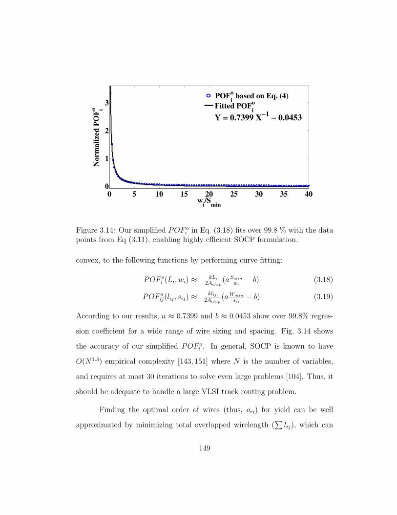
0 5 10 15 20 25 30 35 400
1
2
3
wi/S
min
No
rma
lize
d P
OF
o i
Y = 0.7399 X−1
− 0.0453
POFo
i based on Eq. (4)
Fitted POFo
i
Figure 3.14: Our simplified POF oi in Eq. (3.18) fits over 99.8 % with the data
points from Eq (3.11), enabling highly efficient SOCP formulation.
convex, to the following functions by performing curve-fitting:
POF oi (Li, wi) ≈
kLi
2Achip(aSmin
wi− b) (3.18)
POF sij(lij, sij) ≈
klij2Achip
(aWmin
sij− b) (3.19)
According to our results, a ≈ 0.7399 and b ≈ 0.0453 show over 99.8% regres-
sion coefficient for a wide range of wire sizing and spacing. Fig. 3.14 shows
the accuracy of our simplified POF oi . In general, SOCP is known to have
O(N1.3) empirical complexity [143, 151] where N is the number of variables,
and requires at most 30 iterations to solve even large problems [104]. Thus, it
should be adequate to handle a large VLSI track routing problem.
Finding the optimal order of wires (thus, oij) for yield can be well
approximated by minimizing total overlapped wirelength (∑
lij), which can
149

Algorithm 11 Overall flow of TROY
Input: Global Routing Result GR1: for ∀ layer L ∈ GR do2: wire set C = ∅ //to store contour wires3: for ∀Pi ∈ L in ascending order do4: Wire Ordering with Pi
⋃
C //Solve pMHP5: C = Find contour of Pi
6: end for7: Wire Sizing and Spacing for L //Solve SOCP8: end for
be deduced to a minimum Hamiltonian path (MHP) problem. In spite MHP
is NP-hard, it has been comprehensively studied for several decades, so there
exist highly efficient and near optimal heuristics [93]. As lij solely affects
POF sij, it should have negligible impact on the trade-off between open and
short defects which will be optimally determined by solving SOCP. These
observations motivate our two step approach in Algorithm 11 as follows:
1. Wire Ordering: The goal of wire ordering is to compute yield-maximizing
oij (thus lij). In TROY, wire ordering is done in each panel such that
total overlapped wirelength between adjacent wires is minimized by find-
ing minimum Hamiltonian path (MHP) in order to reduce short defects.
We further propose a variant of MHP, preference aware minimum Hamil-
tonian path (pMHP) to minimize the expected detailed wirelength to-
gether. This is discussed in Section 3.3.2.2.
2. Wire Sizing/Spacing: The goal of wire sizing/spacing is to tune wire
width and spacing such that the maximum immunity to random defects,
150

w3
w4
w5
w2
w1
w6
Sub-panel A Sub-panel Bdisjointing
Figure 3.15: Example of two disjoint subpanels is shown.
thus maximum yield can be achieved. As wire sizing and spacing are
conflicting objectives due to the fixed routing area, the optimal trade-off
is found by second order cone programming (SOCP). This is discussed
in Section 3.3.2.3.
3.3.2.2 Wire Ordering Optimization
The goal of wire ordering is to find an order of wires such that the over-
lapped wirelength (lij) between adjacent wires is minimized to effectively re-
duce POF sij. We first identify a set of disjoint subpanels within each panel such
that there is no shared wire between any two identified subpanels. Fig. 3.15
shows an example of two disjoint subpanels which is similar to the concept of
zone in [239]. Then, wire ordering is performed from the lowest panel to the
highest panel for each subpanel in each panel.
Wire ordering for each subpanel to minimize total overlapped wire-
151

w3
w4
w5
w2
w1 w
6
w3
w4
w5
w2
w1 w
6
09
PiTi Bi
yiel
d
(a)
this
illu
stra
tes
the
trac
kin
gro
uti
ng
pro
ble
min
this
exam
ple
.
w3 w
4 w5
w2
w1
p1
p2
p3
p4
p5
01
23
45
67
89
w6
p6
Pi
(b)
one
feas
ible
routi
ng
solu
tion
can
be
obta
ined
by
inte
rval
pac
k-
ing
algo
rith
m.
w3 w
4 w5
w2
w1
p3
p4
p2
p1
p5
01
23
45
67
89
w6
p6
Pi
M1
M6
M4
M3
M2
M5
M1
M6
M4
M3
M2
M5
(c)
one
opti
mal
solu
tion
from
MH
Pw
ithou
tta
kin
gex
pec
ted
det
aile
dw
ire-
lengt
hin
toac
count.
w3 w
4 w5
w2
w1
p3
p2
p1
p4
p5
01
23
45
67
89
w6
p6
Pi
M1
M6
M4
M3
M2
M5
M1
M6
M4
M3
M2
M5
(d)
anot
her
opti
mal
solu
tion
from
MH
Pw
ith
expec
ted
det
aile
dw
ire-
lengt
hco
nsi
der
ed.
w3 w
4w5
w2
w1
p3
p2
p1
p5
p4
01
23
45
67
89
w6
p6
Pi
wc
wc
Pi-1
M1
M6
M4
M3
M2
M5
M1
M6
M4
M3
M2
M5
(e)
anot
her
opti
mal
solu
tion
from
MH
P,w
hen
bou
ndar
yin
tera
ctio
nis
consi
der
ed.
w3 w
4w5
w2
w1
p3
p6
p1
p5
p4
01
23
45
67
89
w6
p2
Pi
wc
wc
Pi-1
M1
M6
M4
M3
M2
M5
M1
M6
M4
M3
M2
M5
(f)
final
solu
tion
afte
rw
ires
are
size
dan
dsp
aced
for
yie
ldby
SO
CP.
Fig
ure
3.16
:T
RO
Yex
ample
.
152
length can be achieved by well-known minimum Hamiltonian path (MHP) [93,
181, 229]. Consider the example in Fig. 3.16 where six wires (W1 ∼ W6) are
to be routed within a subpanel of a panel Pi for maximum yield. Fig. 3.16 (a)
illustrates the problem in this example. First, assuming minimum wire width
and spacing, a feasible track routing (not exceeding the number of available
tracks) needs to be found through interval packing [88] as shown in Fig. 3.16
(b) which will serve as an initial solution. Other design objectives can be
considered while finding the initial solution, as long as they do not conflict
with the feasibility. Then, a clique as in Fig. 3.17 (a) can be constructed by
regarding each row as a vertex, and edge weight Eij between two rows (thus,
two vertices), Vi and Vj can be computed as follows:
Eij =∑
Wi∈Vi,Wj∈Vj
Lij (3.20)
Since finding a MHP from a clique is well-studied, we skip the details, but
Lin-Kernighan heuristic is shown to be very successful [93]. From the MHP, a
routing solution like Fig. 3.16 (c) may be found. However, a naive MHP ap-
proach has two drawbacks regarding yield, which we further address in TROY.
• The possible detailed wirelength increase due to deviation from the pre-
ferred location (See Section 3.3.1.2) is not considered, which in turn
increases the density of random defects.
• The interaction between adjacent panels is ignored. As short defects can
occur on the boundary of adjacent panels, it is required to take this into
account.
153

w1
w2,6 w3
w4
w5
1 5
7
5
1
4 5
6
2
2
(a) clique for Fig. 3.16 (b)(c)(d) whereedge cost is computed by Eq. (4.2).
w1
w2,6 w3
w4
w5
1 5
7
5
1
4 5
6
2
2
2
3
1
4
3
wc
(b) clique for Fig. 3.16 (e) after adding anew vertex Wc to take boundary interac-tion into account.
Figure 3.17: Clique for wire ordering in TROY.
We observe that there can be multiple optimal MHP solutions, as the
distribution of edge weights is rather narrow. Thus, we need to find the mini-
mum deviation solution estimated by∑
i |pi−Mi| among all the optimal MHP
solutions. We call our modified MHP as preference aware minimum Hamilto-
nian path (pMHP). For example, although both Fig. 3.16 (c) and (d) are the
MHPs of Fig. 3.17 (a) (the same overlapped wirelength), one can recognize that
Fig. 3.16 (d) shows less deviation from the preferred positions (∑
i |pi − Mi|),
which can result in shorter expected detailed wirelength as well as less random
defects.
We further improve our wire ordering by considering the contour of an
adjacent panel. Consider the example in Fig. 3.16 (e) where Wc are the wires
154
from a panel Pk−1, assuming the wires in Pk−1 are already ordered. Fig. 3.16 (e)
shows a better wire ordering than Fig. 3.16 (d), when the interaction between
Pk and Pk−1 is considered. This can be done with a new clique in Fig. 3.17
(b) where Wc is added and set as a starting vertex, and the bold lines indicate
the pMHP. The edge weights between Wc and other vertices can be computed
with Eq. (4.2) as well. When all the panels on a layer are finished with wire
ordering, the wires on the layer will be sized and spaced as in Section 3.3.2.3.
3.3.2.3 Globally Optimal Wire Sizing and Spacing
After wires in every panel on a layer are ordered, the formulation in
Fig. 3.13 can be further deduced to the formulation in Fig. 3.18 after plugging
in Eq. (3.18) and (3.19), filling all the integer variables (oij) with the corre-
sponding values, and eliminating constant terms from the objective. Auxiliary
variables, γij and δi are introduced to translate the nonlinear objective terms
into the rotated conic constraints of Eq. (3.14) which enable second order cone
programming (SOCP) [6,11,28,104,145,156].
In detail, we first set oij = 1 if pi > pj, otherwise oij = 0 based on the
given wire ordering, which will eliminate half of minimum spacing constraints.
Then, we can rewrite the objective function in Fig. 3.13 as follows by setting
Smin = Wmin and taking off all the constant terms:
α∑
i
LiSmin
wi
+ (1 −b
a)di + (1 − α)
∑
i,j>i
lijWmin
sij
(3.21)
With this simplified objective function, we can introduce auxiliary variables,
155

min α∑
i
δi + (1 −b
a)di + (1 − α)
∑
i,j>i
γij
s.t. |pi − Mi| ≤ di ∀i
Smin ≤ sij = pi − pj −wi+wj
2 ∀oij = 1,∀j ∈ ni
lijWmin ≤ sijγij ∀i,∀j ∈ ni
LiSmin ≤ wiδi ∀i
Bk + wi
2 ≤ pi ≤ Tk − wi
2 ∀i ∈ Pk
Wmin ≤ wi ≤ Wmax ∀i
Figure 3.18: After wire ordering is done, the INLP formulation in Fig. 3.13can be casted into highly efficient SOCP.
γij and δi to define the upper bounds of two key terms as follows:
lijWmin
sij
≤ γij (3.22)
LiSmin
wi
≤ δi (3.23)
Hence, Eq. (3.21) can be minimized by suppressing the upper bounds (γij in
Eq. (3.22) and δi in Eq. (3.23)), which is essentially the objective function in
Fig. 3.18. Eq. (3.22) and (3.23) can be further casted into the rotated quadratic
cone in Eq. (3.14). For example, since sij > 0, lij > 0, and Wmin > 0, Eq. (3.22)
is equivalent to
2sijγij ≥ c2ij, cij =
√
(2lijWmin) (3.24)
where cij is a known value, as the wire order defines lij. Since Eq. (3.24) is
in the form of 2x1x2 ≥ ‖x3‖2, x1 ≥ 0, x2 ≥ 0, it describes a rotated quadratic
156

0.5 1 1.5 2 2.5
x 105
0
5
x 105
Th
e n
um
ber
of
con
stra
ints
The number of variables (N)0.5 1 1.5 2 2.5
x 105
0
50
Ru
nti
me
(sec
)
The number of constraintsMeasured runtimeFitted runtime
Y = 3e−6 X1.335
− 0.2701
Figure 3.19: The empirical runtime complexity of our SOCP is O(N1.335) whereN is the number of variables. Such near linear complexity makes TROY tolarge scale VLSI track routing.
cone in Eq. (3.14). The same transformation can be done for Eq. (3.23).
Then, the formulation in Fig. 3.18 can be solved optimally and efficiently by a
primal-dual interior-point method with O(N1.3) empirical bound where N is
the number of variables [143, 151], thus the solution will provide the optimal
wire sizing and spacing for maximum yield.
Fig. 3.19 shows the empirical runtime complexity of our SOCP formula-
tion in TROY. The number of constraints is linearly proportional to the num-
ber of variables. Hence, even with a larger circuit, the number of constraints
will not explode, and the problem size will be tractable. When we perform
curve fitting to the measured runtime samples, it has O(N1.335) where N is
157

the number of variables.
The optimal wire sizing and spacing for an entire layer by SOCP can
find the optimal trade-off between open and short defects in terms of yield.
Thus, TROY is much superior to traditional local or iterative approaches.
Fig. 3.16 (f) shows a track routing solution after wire sizing and spacing are
done by SOCP. Intuitively, the longer overlapped wirelength (lij) between
two adjacent wires needs wider spacing to minimize POF sij. Meanwhile, the
spacing has to be larger than minimum spacing (Smin) at least, and all the
wires should be posed within the corresponding panel. If the wire has enough
space around it, the wire width will be increased to minimize POF oi . Even
though this example shows a case for one panel, wire sizing and spacing will
be performed for all the wires in a layer by a single SOCP formulation. In
practice, the wire width may be discrete. For such cases, we can change the
continuous wire width found from SOCP to the closest discrete wire width
which does not violate the minimum wire spacing rule.
For some designs, aggressive wire sizing can cause routing congestion
for local wires by leaving insufficient space. The seriousness of this issue can
be different in different layers, as lower layers tend to be more crowded by
local wires. This issue can be overcome in TROY by adjusting α parameter in
the objective function in Fig. 3.18. By apply smaller value, TROY will search
for the solution with higher weight on short defect optimization, which will
increase the spacing between wires for local wires. Therefore, in higher layers,
aggressively configured TROY can be applied, while conservative approach
158

1 2 3 4 5 6 7
x 104
0
10
20
30
40
50
60
The number of cells (C)
Ru
nti
me
(sec
)
Y = 3.567e−5 X1.276
− 1.99
Measured runtimeFitted runtime
Figure 3.20: The average empirical runtime complexity of our SOCP for onelayer is O(C1.276) where C is the number of cells.
can be taken in lower layers.
3.3.2.4 Runtime Complexity Analysis
As TROY consists of two steps, we will analyze the runtime complexity
of each step to get the overall complexity.
1. Wire Ordering: The main bottleneck in wire ordering is to find pMHP.
However, we can regard the time complexity of finding pMHP as con-
stant, as the number of maximum wires in a panel is fixed by the global
routing cell size. Hence, the complexity of each pMHP instance does
not scale according to the design size. Let L and C denote the number
of layer and the number of cells (the chip area) respectively. Then, the
159

runtime complexity of wire ordering is O(LC).
2. Wire Sizing/Spacing: The complexity of SOCP is shown as O(N1.335)
in Fig. 3.19. However, since the relationship between the number of
variables and the number of cells is not clear, we empirically measure
the runtime complexity of SOCP w.r.t. the number of cells. As shown
in Fig. 3.20, it has O(C1.276) where C is the number of cells. Since
SOCP needs to be solved for each layer, the runtime complexity of wire
size/spacing is O(LC1.276).
Therefore, the overall runtime complexity of TROY can be shown as
O(LC1.276) based on our analysis, which can be fast enough for a large scale
VLSI design.
3.3.3 Experimental Results
We implement TROY in C++. The initial global routing results are
generated from the publicly available BoxRouter in Section 2.3. All the ex-
periments are performed on a 3.0 GHz Pentium machine with 1GB RAM.
A solver in [93, 97] is properly modified to find preference aware minimum
Hamiltonian path (pMHP) for wire ordering in Section 3.3.2.2, and MOSEK
4.0 [104] is used to solve second order cone programming (SOCP) for wire
sizing and spacing in Section 3.3.2.3. Since the ISPD98 IBM benchmarks are
lack of technology information, we assume 0.13µm technology to use the defect
size distribution parameter in [68], and set Smin=Wmin=0.2µm. We further as-
sume that Wmax=0.4µm, and 0.2, 0.3 and 0.4µm are only allowed wire widths.
160

Table 3.3: ISPD98 IBM benchmarks.circuit global routing result
name cells nets wires grids g.sa(µm2) wlenb(µm)ibm01 12036 11507 35K 64x64 26.9 135172ibm02 19062 18429 68K 80x64 119.7 1049388ibm03 21924 21621 56K 80x64 96.0 899694ibm04 26346 26163 73K 96x64 73.6 714612ibm05 28146 27777 110K 128x64 423.4 4917756ibm06 32185 33354 112K 128x64 105.6 1693308ibm07 44848 44394 141K 192x64 121.0 2652531ibm08 50691 47944 160K 192x64 107.5 2456022ibm09 51461 50393 156K 256x64 62.7 2094085ibm10 66948 64227 216K 256x64 172.8 4701936
a global routing cell sizeb global wirelength
Table 3.3 shows the detail for each benchmark circuit. Since the benchmarks
are lack of detailed pin locations, 1-5 pins for each global routing cell on each
wire are randomly generated to define the preferred position of each wire (Mi).
Monte-Carlo simulation [215] with 10K random defects based on Eq. (3.8) is
performed to estimate yield loss. Also, these random defects are assumed to
be uniformly distributed on the chip for fair estimation. Fig. 3.21 shows our
defect distribution.
We explore the trade-off between random defects controlled by α in
Section 3.3.2.1, assuming continuous wire width. In Fig. 3.22 (a), yield loss
changes due to open and short defects by different α values are plotted for all
the benchmark circuits in Table 3.3. Overall, with larger α, yield loss due to
open defects decreases at a cost of more short defects. Fig. 3.22 (b) shows total
yield loss (short+open defects) by different α, and indicates that the minimum
161

0 10 20 30 40 500
1K
2K
3K
4K
5K
Normalized defect size
Th
e n
um
ber
of
def
ects
Figure 3.21: The distribution of 10K defects for Monte-Carlo simulation isshown.
yield loss can be obtained around α = 0.6. Although whether the open defects
are dominant over the short defects or not is still controversial [68,70,120,130],
our result (α = 0.6) shows that both are similarly important. We set α = 0.6
for all the experiments.
For comparison, we implement a greedy algorithm similar to [208], the
only track routing algorithm which can handle arbitrary wire spacing to our
best knowledge. As the original algorithm in [208] optimizes crosstalk and
timing without wire sizing, we add wire sizing feature along with wire spac-
ing functionality. We also modify the optimization objective such that its
wire ordering and wire sizing/spacing greedily seek for minimization of POF o
and POF ss. Let these greedy wire ordering and wire sizing/spacing denote
g.wo and g.wss, while MHP-based wire ordering and SOCP-based wire siz-
ing/spacing denote h.wo and s.wss.
162

Tab
le3.
4:C
ompar
ison
bet
wee
ngr
eedy
trac
kro
ute
ran
dT
RO
Y(α
=0.
6).
algo
rith
mev
aluat
ion
ibm
01ib
m02
ibm
03ib
m04
ibm
05ib
m06
ibm
07ib
m08
ibm
09ib
m10
sum
rati
oop
en52
766
066
669
256
877
658
769
168
159
964
471.
00g.
woa
def
ects
gsh
ort
521
513
457
527
406
507
453
481
539
456
4860
1.00
+g.
wss
bto
tal
1048
1173
1123
1219
974
1283
1040
1172
1220
1055
1130
71.
00(d
.wd
e)
wle
nin
ch(µ
m)19
606.
697
720.
269
128.
086
668.
529
0296
.013
9420
.222
4507
.620
1960
.816
8111
.344
649.
216
4206
8.3
1.00
cpu
(sec
)1
11
12
24
45
728
1.00
open
414
482
484
515
391
612
393
518
470
387
4666
0.72
h.w
ocdef
ects
shor
t63
560
957
166
253
864
654
163
466
654
860
501.
24+
g.w
ssto
tal
1049
1091
1055
1177
929
1258
934
1152
1136
935
1071
60.
95(d
.wd)
wle
nin
c(µ
m)19
626.
295
338.
969
544.
688
901.
828
7752
1403
44.5
2241
30.2
2061
26.6
1714
98.7
3465
90.2
1649
853.
71.
00cp
u(s
ec)
764
3019
164
3859
3529
9353
819
.21
open
454
584
523
567
388
657
506
541
581
504
5305
0.82
g.w
odef
ects
shor
t51
849
045
552
534
158
243
050
553
543
948
200.
99+
s.w
ssd
tota
l97
210
7497
810
9272
912
3993
610
4611
1694
310
125
0.90
(d.w
d)
wle
nin
c(µ
m)19
052.
996
149.
468
154.
686
960.
428
6044
.913
8334
.921
8944
.220
0589
.416
5633
.833
7722
.716
1758
7.2
0.99
cpu
(sec
)10
2923
3358
5576
8386
125
579
20.6
8
open
561
511
519
618
389
671
459
562
551
441
5282
0.82
TR
OY
def
ects
shor
t32
044
544
739
929
349
135
142
542
337
639
700.
82(d
.wd
e )to
tal
881
956
966
1017
682
1162
810
987
974
817
9252
0.82
wle
nin
c(µ
m)19
119.
794
747.
668
808.
388
547.
129
2148
.413
9782
.822
1714
.320
5223
.816
9543
.334
4612
.416
4424
7.7
1.00
cpu
(sec
)13
9050
5021
787
131
117
110
214
1079
38.5
4
open
547
539
532
612
391
679
461
582
553
447
5343
0.83
TR
OY
def
ects
shor
t31
040
739
637
927
846
332
839
340
834
437
060.
76(c
.wd
f)
tota
l85
794
692
899
166
911
4278
997
596
179
190
490.
80w
len
inc
(µm
)19
119.
794
747.
668
808.
388
547.
129
2148
.413
9782
.822
1714
.220
5223
.816
9543
.234
4612
.416
4424
7.5
1.00
cpu
(sec
)13
9051
5021
886
136
116
108
219
1087
38.8
2a
gree
dy
wir
eor
der
ing
bit
erat
ive
gree
dy
wir
esi
zing/
spac
ing
cpre
fere
nce
awar
em
inim
um
Ham
ilto
nia
npat
hbas
edw
ire
order
ing
inSec
tion
3.3.
2.2
dse
cond
order
cone
pro
gram
min
gbas
edw
ire
sizi
ng/
spac
ing
inSec
tion
3.3.
2.3
edis
cret
ew
ire
wid
th(W
min,1.
5Wm
in,an
d2W
min
are
allo
wed
.)f
conti
nuou
sw
ire
wid
th(a
ny
wir
ew
idth
bet
wee
nW
min
and
2Wm
in
are
allo
wed
.)g
esti
mat
edbas
edon
Mon
te-C
arlo
sim
ula
tion
[215
]w
ith
10K
random
def
ects
hex
pec
ted
det
aile
dw
irel
engt
h(t
he
sum
mat
ion
ofth
edev
iati
onof
each
wir
efr
omit
spre
ferr
edlo
cati
on)
163

0 0.2 0.4 0.6 0.8 12
4
6
8
Yie
ld l
oss
du
e to
op
en d
efec
ts (
%)
α0 0.2 0.4 0.6 0.8 1
2
4
6
8
Yie
ld l
oss
du
e to
sh
ort
def
ects
(%
)
0 0.2 0.4 0.6 0.8 12
4
6
8
Yie
ld l
oss
du
e to
sh
ort
def
ects
(%
)
0 0.2 0.4 0.6 0.8 12
4
6
8
Yie
ld l
oss
du
e to
sh
ort
def
ects
(%
)
0 0.2 0.4 0.6 0.8 12
4
6
8
Yie
ld l
oss
du
e to
sh
ort
def
ects
(%
)
0 0.2 0.4 0.6 0.8 12
4
6
8
Yie
ld l
oss
du
e to
sh
ort
def
ects
(%
)
0 0.2 0.4 0.6 0.8 12
4
6
8
Yie
ld l
oss
du
e to
sh
ort
def
ects
(%
)
0 0.2 0.4 0.6 0.8 12
4
6
8
Yie
ld l
oss
du
e to
sh
ort
def
ects
(%
)
0 0.2 0.4 0.6 0.8 12
4
6
8
Yie
ld l
oss
du
e to
sh
ort
def
ects
(%
)
0 0.2 0.4 0.6 0.8 12
4
6
8
Yie
ld l
oss
du
e to
sh
ort
def
ects
(%
)
2
4
6
8
Yie
ld l
oss
du
e to
sh
ort
def
ects
(%
)
Short defectOpen defect
(a) With larger α, the number of open defects decreases, while thenumber of short defects increase.
0 0.2 0.4 0.6 0.8 16
8
10
12
14
Yie
ld l
oss
(%
)
α
(b) The minimum yield loss due to random defects (both open andshort defects) can be achieved around α = 0.6.
Figure 3.22: Trade-off between open and short defects is shown by α.
Table 3.4 investigates the effect of two main techniques in TROY by
pairing each technique with a greedy algorithm (h.wo+g.wss and g.wo+s.wss),
and compares TROY (α = 0.6) with a greedy yield-driven track router (g.wo+g.wss).
164
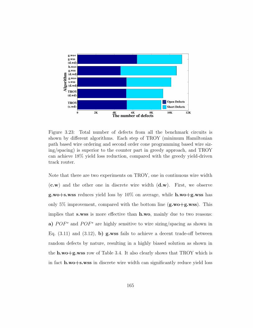
0 2K 4K 6K 8K 10K 12K
The number of defects
Alg
ori
thm
g.wo+
g.wss
(d.wd)
h.wo+
g.wss
(d.wd)
g.wo+
s.wss
(d.wd)
TROY
(d.wd)
TROY
(c.wd)
Open Defects
Short Defects
Figure 3.23: Total number of defects from all the benchmark circuits isshown by different algorithms. Each step of TROY (minimum Hamiltonianpath based wire ordering and second order cone programming based wire siz-ing/spacing) is superior to the counter part in greedy approach, and TROYcan achieve 18% yield loss reduction, compared with the greedy yield-driventrack router.
Note that there are two experiments on TROY, one in continuous wire width
(c.w) and the other one in discrete wire width (d.w). First, we observe
g.wo+s.wss reduces yield loss by 10% on average, while h.wo+g.wss has
only 5% improvement, compared with the bottom line (g.wo+g.wss). This
implies that s.wss is more effective than h.wo, mainly due to two reasons:
a) POF o and POF s are highly sensitive to wire sizing/spacing as shown in
Eq. (3.11) and (3.12), b) g.wss fails to achieve a decent trade-off between
random defects by nature, resulting in a highly biased solution as shown in
the h.wo+g.wss row of Table 3.4. It also clearly shows that TROY which is
in fact h.wo+s.wss in discrete wire width can significantly reduce yield loss
165

by 18% on average, and it can be even over 30% for ibm05, compared with
the greedy approach (g.wo+g.wss) in discrete wire width. Also, the total
number of open and short defects is consistently reduced. The discrete wire
width incurs only 2.2% more yield loss on average, when TROY in discrete
wire width (d.w) and continuous wire width (c.w) are compared. Fig. 3.23
summarizes the key results of Table 3.4.
Although the runtime becomes longer, all benchmarks can be finished
within a few seconds/minutes. More importantly, TROY has near linear run-
time complexity as discussed in Section 3.3.2.4. Therefore, it should be appli-
cable to large scale VLSI designs.
3.4 Detailed Routing for Lithography Enhancement
Lithography with 193nm wavelength is one of the most fundamental
challenges due to its impact on yield and timing, and expected to be more
serious in more advanced technologies. Even worse, next generation lithogra-
phies are not likely to be in the mainstream in the near future. As of now,
the 193nm (wavelength) optical lithography is still the dominant integrated
circuit manufacturing process for 65nm and 45nm nodes, and next generation
lithographies are not likely to be in the mainstream in the near future [141].
Accordingly, major IC manufacturers still use 193nm lithography to print 65,
45, 32nm and below, heavily relying on resolution enhancement techniques
such as optical proximity correction (OPC).
OPC modifies GDSII for better printability as a post-tapeout mask
166

synthesis, and becomes a crucial manufacturing step in sub 90nm designs but
at a cost of high computational complexity as well as mask cost overhead.
Nevertheless, OPC may be too late to make all the necessary corrections due
to restricted design flexibility. These drawbacks of OPC put lithography aware
design (as a part of design-for-manufacturability (DFM)) in greater demand
than ever so that the downstream lithography and OPC effects can be ab-
stracted and estimated for better design decisions in terms of manufacturabil-
ity and manufacturing cost.
As a result, there are many manufacturability aware efforts in earlier
design stages such as logic synthesis and placement [87, 109], but routing is
often believed to be one of the most important stages to address the lithog-
raphy issue due to the following reasons [110, 154]: (a) wire printability is
coupled with interconnection network which is mainly determined by routing,
(b) routing is the last major VLSI physical design step before manufactur-
ing, thus has more comprehensive and accurate information on lithography,
(c) routing still has considerable design flexibility to find reasonable trade-off
between printability and conventional design objectives (e.g., timing, noise,
power). These factors lead to a lot of recent academic and industrial efforts
in lithography aware routing, especially detailed routing due to small influence
window of optical lithography.
One easy approach for lithography aware routing would be to introduce
manufacturability aware rules, but such rule-based approaches suffer from the
exploding number of rules, expensive rule-checking, and more importantly
167

large area/timing overhead due to over guard-band. These difficulties lead to
several model-based approaches. The first OPC aware maze routing is pro-
posed in [110] based on multi-constrained shortest path optimization by a
subgradient method. A multilevel routing approach to minimize the number
of OPC features is studied in [44]. As a post-optimization, ripup/rerouting to
remove litho-hotspots is proposed based on fast lithography simulation [154]
or pattern matching [129]. However, there are a few drawbacks in these prior
works: (a) printed or silicon image is not directly addressed [44, 110], (b)
the result is not verified with an industrial sign-off tool under inevitable de-
focus [44, 110, 154], (c) the burden of trivial litho-hotspots which can be eas-
ily fixed by OPC is imposed on a router by ignoring OPC [154], (d) post-
optimization inherently cannot make radical changes enough to address lithog-
raphy issues [129,154].
In this section, we propose ELIAD, an efficient lithography aware de-
tailed router based on a compact and high fidelity post-OPC litho-metric. Our
litho-metric shows high correlation (>0.95) to total EPE computed by Calibre-
OPC/ORC in large scale. We plug this metric into ELIAD using Lagrangian
relaxation. The major contributions of this section include the following:
• We show with very comprehensive simulation data that a pre-OPC met-
ric cannot guide lithography aware detailed routing accurately.
• We propose a compact and high fidelity litho-metric with OPC taken
into account. Our metric is from statistical weak grid characterization
168

which has several advantages over pattern characterization.
• We present an efficient lithography aware detailed router, ELIAD to opti-
mize post-OPC silicon image. In our formulation, we adopt the proposed
litho-metric in ELIAD based on a Lagrangian relaxation technique.
• We propose a technique for fast convergence of subgradient optimization
using weak grid shadowing around blockages and routed nets
• ELIAD is the first lithography aware detailed router targeting post-OPC
image in a correct-by-construction fashion. Routing results are verified
with an industrial optical rule check (ORC) under a realistic OPC recipe.
The rest of the section is organized as follows. Section 3.4.1 provides
a comprehensive survey on previous work. Section 3.4.2 stresses the impor-
tance of post-OPC EPE metric, followed by our proposed litho-metric in Sec-
tion 3.4.3. Section 3.4.4 proposes ELIAD. Experimental results are discussed
in Section 3.4.5.
3.4.1 Previous Works
Optical projection systems in modern optical lithography technology
usually use partially coherent illumination. Illustration of a typical optical
lithography system is shown in Fig. 3.24. Since a partially coherent system
can be approximately decomposed into a small number of P fully coherent
systems [110,179], the aerial image intensity I(x, y) at the point (x, y) can be
169
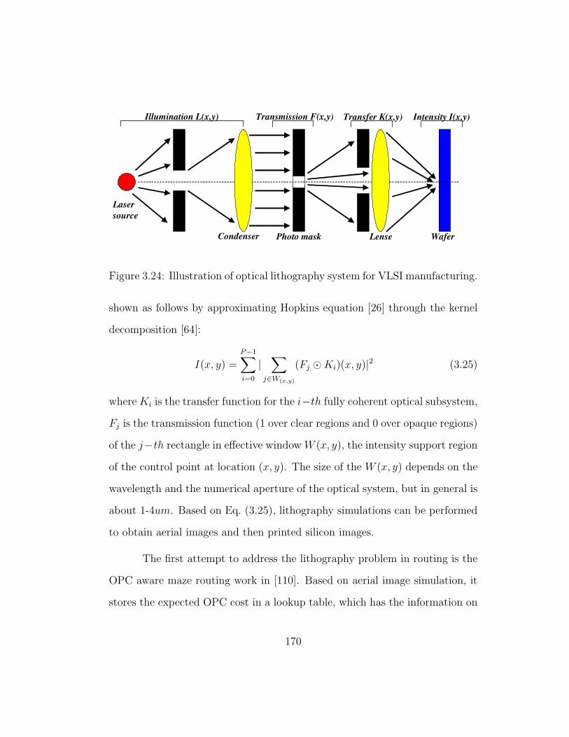
Laser
source
Condenser Photo mask Lense Wafer
Illumination L(x,y) Transmission F(x,y) Transfer K(x,y) Intensity I(x,y)
Figure 3.24: Illustration of optical lithography system for VLSI manufacturing.
shown as follows by approximating Hopkins equation [26] through the kernel
decomposition [64]:
I(x, y) =P−1∑
i=0
|∑
j∈W(x,y)
(Fj ⊙ Ki)(x, y)|2 (3.25)
where Ki is the transfer function for the i−th fully coherent optical subsystem,
Fj is the transmission function (1 over clear regions and 0 over opaque regions)
of the j−th rectangle in effective window W (x, y), the intensity support region
of the control point at location (x, y). The size of the W (x, y) depends on the
wavelength and the numerical aperture of the optical system, but in general is
about 1-4um. Based on Eq. (3.25), lithography simulations can be performed
to obtain aerial images and then printed silicon images.
The first attempt to address the lithography problem in routing is the
OPC aware maze routing work in [110]. Based on aerial image simulation, it
stores the expected OPC cost in a lookup table, which has the information on
170
the interference from patterns at different length by distance. While routing
a new pattern, the interferences from all existing patterns in its influence
window are looked up from the table, and then summed up to evaluate the total
optical interference from existing patterns. Meanwhile, the optical interference
(OPC cost) on existing patterns due to the new pattern is estimated using
the maximum interference on these patterns. Then, a vector-weighted graph
method is applied to map the grid routing model to a graph, where the edge
cost is a vector consisting of the interferences from existing patterns as well
as the interference of a new pattern to existing patterns. With such vector-
weighted graph, OPC aware maze routing can be casted as a multi-constrained
shortest path problem which is then solved by Lagrangian relaxation. It shall
be noted that optical interference is not a direct lithography metric, while the
edge placement error (EPE) widely used in OPC algorithms is.
Another lithography aware maze routing algorithm is proposed in [232]
where a table of EAD (electric amplitude of diffraction) is pre-built, and the
OPC error is estimated as the square of the accumulated EAD values from the
patterns within process window. Then, it greedily performs maze routing such
that a routed path for each net does exceed neither an OPC error threshold
nor a path length constraint. Again, it shall be noted that the EAD square
metric is not a direct/verified lithography measurement.
The RADAR work [154] is the first attempt to directly link a lithogra-
phy simulator (using the direct edge placement error metric) to detailed rout-
ing. Based on fast lithography simulation techniques which are more suitable
171

Figure 3.25: Convolution lookup for fast lithography simulation [241].
for full-chip simulations, it generates so-called lithography hotspot maps to
guide post-routing optimization, namely wire spreading and ripup/rerouting.
As an example to measure the lithography and RET effort, the edge placement
error (EPE) metric is used. To compute EPE efficiently, [154] utilized an ef-
fective kernel decomposition method and fast table-lookup techniques. In the
kernel decomposition based simulation, a core computational step is the convo-
lution term. Due to the linearity of convolution in Eq. (3.25), the convolution
for any arbitrary rectangle inside the effective window can be decomposed into
four upper-right rectangles which can reduce the table size significantly [154],
as shown in Fig. 3.25. After the EPE map is obtained from fast lithography
simulations, wire spreading and ripup/rerouting can be applied to eliminate
the EPE hotspots and to improve printability. The fast lithography simu-
172

lator is called during routing modification if needed to make sure no new
lithography hotspots occur. The result implies that both wire spreading and
ripup/rerouting are effective in removing EPE hotspots, but ripup/rerouting
can be more effective than wire spreading with less wirelength overhead.
A similar ripup/rerouting approach is proposed in [129]. However, dif-
ferently from [154], effective pattern searching is adopted, i.e., a set of known
undesirable patterns are stored/matched to identity lithography hotspots. Then,
the identified undesirable routing patterns are either removed or modified by
performing ripup/rerouting. Recently, a multilevel routing approach to min-
imize the number of OPC features is studied in [44]. A simple OPC cost
which becomes higher for longer and wider wires is proposed and applied as a
factor in maze routing. It shall be noted that the lithography aware routing
is still in its infancy, and there are many research issues to achieve holistic
understanding for it.
3.4.2 Pre-OPC and Post-OPC EPE Comparison
In all the previous papers in Section 3.4.1, the lithography optimization
is performed based on pre-OPC metrics. However, considering the strength
of industrial OPC algorithms/tools, pre-OPC metrics can significantly mis-
guide optimization. To understand the correlation between pre-OPC EPE
and post-OPC EPE as well as the performance of the state-of-the-art OPC
algorithms, we collect 0.5M sampling locations from a 65nm industrial design.
For each sampling location, we measure pre-OPC EPE and post-OPC EPE
173

Potential Real Litho-Hotspots
Figure 3.26: This plot shows how a pre-OPC EPE distribution will be mappedto a post-OPC EPE distribution. From this result, we can conclude that mostpre-OPC EPE hotspots will be taken care of by OPC algorithms. Therefore,a lithography aware detailed router should use a post-OPC EPE metric tocapture real litho-hotspots rather than to optimize trivial easy-to-fix-by-OPChotspots with design overhead (e.g., wirelength, runtime, via, and so on).
to build a mapping table. Please see Section 3.4.5 for details. Fig. 3.26 il-
lustrates the correlation by plotting how pre-OPC EPE (on the x axis) can
be mapped to post-OPC EPE (on the y axis). Overall, it shows that an in-
dustrial strength OPC algorithm can effectively reduce EPE, resulting in no
correlation between pre-OPC EPE and post-OPC EPE (R = −0.36). Espe-
cially, it shows impressive OPC performance in optimizing the litho-hotspots
with relatively large pre-OPC EPE (e.g., > 15nm). Most of such hotspots
are largely eliminated by reducing EPE to about 5nm. However, a small por-
174

tion of such pre-OPC litho-hotspots remain as real post-OPC litho-hotspots
even after OPC as shown in Fig. 3.26. As no litho-hotspot is allowed for chip
tape-out, such post-OPC litho-hotspots should be fixed through design modifi-
cation. The result in Fig. 3.26 leads to several key observations for lithography
aware design optimization, stressing the criticality of a post-OPC EPE metric
as follows:
• Since an advanced OPC algorithm is highly effective in improving print-
ability, optimizing pre-OPC litho-hotspots during design time can incur
unnecessary design overhead in terms of wirelength, timing, noise, and
so on.
• As OPC is a must-step in sub 90nm nodes, design time lithography
optimization should focus on real post-OPC litho-hotspot elimination.
We further analyze the patterns of post-OPC litho-hotspots and find
out highly frequent occurrence of singular grids (e.g., line-end, jog-corner, via,
and so on) around such hotspots. There are two intuitive explanations behind
this finding: a) OPC algorithms cannot converge efficiently, when there are
multiple singular grids in the process window; b) OPC receipts are tuned for
the most common case which is two paralleled running wires. This observation
leads us to the characterization of such cases, which becomes one of key ideas
in our post-OPC printability metric as in Section 3.4.3.
175

3.4.3 Post-OPC Printability Prediction
In this subsection, we present our litho-metric to predict post-OPC
printability during detailed routing. The focus of our metric is to estimate
the impact of a routing decision on global (large scale) printability in faster
time, so that it can be plugged in as a part of a detailed router. We intend to
neither compute the exact EPE of a certain spot nor identify litho-hotspots
accurately. We are mainly interested in guiding a router to generate a more
litho-friendly layout by capturing global trend at a small cost. In this aspect,
our metric is different from another fast hotspot detection using graph in [121],
and more suitable for a detailed router.
The motivation behind OPC consideration in our metric is that a pat-
tern which is believed to be litho-unfriendly can be printed successfully de-
pending on OPC algorithms and recipes. Considering OPC as an essential
step, a litho-metric or fast lithography simulation [154,238] without OPC can
burden a detailed router unnecessarily by blindly optimizing some easy-to-fix-
by-OPC litho-hotspots.
In Section 3.4.3.2, we propose our litho-metric using the statistical weak
grid type (WGT) characterization in Section 3.4.3.1. Section 3.4.3.3 shows the
high fidelity of our metric.
3.4.3.1 Statistical WGT Characterization
In industry, pattern matching has been done to identify litho-unfriendly
patterns, so that it can be used in post-optimization for litho-hotspot removal.
176

Also, it can yield very accurate hotshot detection even in fine scale, if a pattern
library is comprehensive enough. However, pattern matching is inefficient in
guiding a detailed router in a correct-by-construction manner for the following
reasons:
• Runtime: Pattern matching is computationally too expensive to be
used in a detailed router even with the latest algorithm [235, 238], as
detail routing is already one of the slowest steps in a VLSI design flow.
• Memory: Depending on technology, the number of patterns we need to
store can explode. Therefore, it may consume too large memory for an
already-memory-hungry detailed router.
• Update: Whenever there is a change in either process technology or
OPC recipe, the characterization needs to be redone to reflect the latest
fab condition. However, pattern characterization for pattern matching
requires long time and huge effort due to the large number of possibilities.
• Decomposability: Pattern matching cannot be done incrementally due
to the lack of decomposability. Any change in layout should invoke a new
pattern matching, as the change cannot be decomposed from the original
layout. Considering many ripup/reroutings in a detailed router, pattern
matching is not efficient.
Therefore, we propose a simple yet effective weak grid type characterization
scheme based on the following definitions:
177

line-end
jog-corner
t1
t2
(a)
t1
t2
(b)
t1
t2
(c)
t1
t2
(d)
t1
t2
(e)
Figure 3.27: WGT characterization for t1=jog-corner and t2=line-end is shownwhere (b), (c), (d), and (e) are the cases with the same distance. Thus, themean EPE will characterize this interaction between t1 and t2 at this distance.
• Weak grid (WG) is defined as a detailed routing grid filled with one of
the predefined litho-prone shapes.
• Weak grid type (WGT) is defined as the type of the litho-prone shape
embedded on the corresponding WG.
Fig. 3.27 (a) shows an example of two WGTs, a jog-corner and a line-end.
Based on given predefined shapes which are highly prone to lithography or
critical dimension (CD) variation, the interference between WGT is studied
statistically.
We describe our statistical WGT characterization in Algorithm 12. The
first input is a set of WGT, T which includes via, jog-corner, line-end, fat-
wire-edge, and so on. The second input is the maximum distance at which
two types from T can interfere (typically less than 0.8um). Then, as in line
178

Algorithm 12 Statistical WGT Characterization
Input: A set of WGT T , a max distance d1: Table WGT TABLE ⇐ ∅2: for each type t1 ∈ T do3: for each type t2 ∈ T do4: for i = 1 to d do5: P = a set of patterns which have one t1 and one t2 with the distance
= i6: sum = 07: for each pattern p ∈ P do8: lithography simulation of p after OPC9: for each EPE hotspot h ∈ p and ≥ noise do
10: sum += EPE of h11: end for12: end for13: WGT TABLE(t1, t2, i) = sum
|P |
14: end for15: end for16: end forOutput: WGT TABLE
5, we enumerate multiple patterns w.r.t. two types at various distances to see
the relation between distance and a pair of WGTs. After performing OPC
and lithography simulation for each pattern as in line 8, we compute a mean
EPE for a triple which consists of two WGTs and distance as in line 13.
While computing the mean, we ignore noise/minor EPE hotspots (in our case,
≤ 5nm) as in line 9. Hence, the mean EPE statistically represents printability
as a function of distance. Fig. 3.27 (b)-(e) show some example patterns with
the same distance between the jog-corner and the line-end.
In typical case, the number of WGTs would be around 10, and the
number of patterns for each pair of WGTs would be like 50. Thus, the total
179

Algorithm 13 WG Shadowing
Input: A Table WGT TABLE, a grid e, a set of WGTs T , a max distance d1: G= a set of grids within d from e/e2: t= a WGT embedded at e3: for each grid g ∈ G do4: for each type t∗ ∈ T do5: g.cost[t∗]+=WGT TABLE(t, t∗,dist from g to e)6: end for7: end for
number of cases is about 10· (10−1)2
·50 = 2250 which can be done in a few hours
including OPC (also one time job!). Therefore, the characterization update
can be done in short time, and each characterization triple (the line 13 of
Algorithm 12) needs only 4 bytes and O(1) access time by table lookup.
Consequently, with statistical WGT characterization, we can see ad-
vantages over pattern characterization in terms of runtime and space. More-
over, as any polygon can be decomposed into grids geometrically, we can esti-
mate printability incrementally, which is critical for a detailed router. Then,
the question is about the fidelity of our metric, which will be shown in Sec-
tion 3.4.3.3.
3.4.3.2 Compact Litho-Metric with OPC
After the characterization, we can use it to estimate printability during
detailed routing. We propose the following litho-metric for a detailed routing
grid e:
litho(e) =
e.cost[t] if WGT of e = t0 otherwise
(3.26)
180

C F F F F C
F F F F C
E
F
6,54,32,11,0
4,32,1
3,21,1
4,32,1
3,32,12,21,0
3,32,11,11,0
4,42,31,10,0
1,10,0
1,10,0
1,10,0
3,32,1
3,32,1
4,42,3
1,10,04,42,3
4,42,3
6,43,3
3,21,1
1,10,0
6,43,3
6,43,36,43,3
6,43,3
6,43,3
2,21,12,21,1
2,21,1
2,21,1
2,21,1
4,42,2
4,42,2
4,42,2
4,42,2
4,42,2
4,42,2
4: line-end3: jog-corner2: via1: wire
(a) WG Shadowing is performedalong the contour of the blockage.Hence, grids within a certain dis-tance get shadowed by a cost array.
C F F F F C
F F F F C
E
F
6,54,32,11,0
4,32,1
3,21,1
4,32,1
3,32,12,21,0
3,32,11,11,0
4,42,31,10,0
1,10,0
1,10,0
1,10,0
3,32,1
3,32,1
4,42,3
1,10,04,42,3
4,42,3
6,43,3
3,21,1
1,10,0
6,43,3
6,43,36,43,3
6,43,3
6,43,3
2,21,12,21,1
2,21,1
2,21,1
2,21,1
4,42,2
4,42,2
4,42,2
4,42,2
4,42,2
4,42,2
E
EJ
J
(b) WG Shadowing needs to be per-formed along the routed wire. Thus,the costs in the arrays of the greygrids will be updated/increased.
Figure 3.28: Respectively assuming C, F, E, and J are blockage-corner, fat-wire-edge, line-end, and jog-corner, WG Shadowing examples are shown. Eachgrid has a cost array which contains the costs for jog-corner, line-end, via, andwire.
where e.cost[t] is a lithography cost computed by Algorithm 13. Fig. 3.28
shows a simple example of WG Shadowing around a blockage and a net. For
each WG, we will shadow neighboring grids within the maximum distance.
While shadowing a grid, we prepare costs for all possible WGTs so that the
grid has a cost array as in line 5 in Algorithm 13. In Fig. 3.28 (a), each grid has
four costs which will penalize any new polygon passing it by the corresponding
cost. Later, if a wire is embedded in one of these shadowed grids, it gets a
lithography penalty based on the WGT (e.g., whether a via is dropped, a line
is ended, and so on) by Eq. (3.26). After the wire is embedded, we will perform
WG Shadowing for grids around the wire as in Fig. 3.28 (b).
181

2 3 4 520
40
60
80
100
120
Normalized Distance
Norm
ali
zed
Lit
ho−
Met
ric
jog−corner and wire
line−end and wire
(a) According to our WGT characterization, line-end is cheaper thanjog-corner when faced with wire.
wire
DC
AB
jog-corner
(b) wirelength-driven.
wire
DC
AB
line-end
(c) litho-metric aware.
Figure 3.29: A-B-C-D are connected based on wirelength in (b), but litho-metric in (c).
Unlike design rules, we can quantify the interaction between two WGTs
in order to make beneficial trade-off among various routing patterns or design
objectives. As in Fig. 3.29 (a), line-end is cheaper than jog-corner when inter-
acting with wire, although litho-metrics of both decrease sharply with longer
distance. Hence, our metric based on the characterization in (a) prefers the
182

layout in (c) to that in (b) for better printability at a cost of wirelength.
3.4.3.3 High Fidelity of Our Litho-Metric
We evaluate the fidelity of our litho-metric by comparing with Calibre-
OPC/ORC (for detailed setup, see Section 3.4.5). Fig. 3.30 proves the high
fidelity of our litho-metric where Y axis is the summation of EPEs. We collect
the samples from industrial 65m design layouts, while varying the sample size
from 8x8um2 to 32x32um2. When the sample area is 8x8um2 as in Fig. 3.30
(a) and (b), it does not correlate with the simulation result well enough to
guide a detailed router. However, the larger the sample area is, the better it
correlates, as shown in Fig. 3.30 (c), (d), (e), and (f). When the sample area
is 32x32um2, it correlates more than 95% for both M1 and M2 where the most
number of litho-hotspots occur. The reason for higher fidelity for the larger
sample is because we take the average of EPE for each distance during WGT
characterization as line 13 of Algorithm 12. With smaller sample area where
we may get some extreme cases, the prediction can deviate from the real trend.
Statistically, however, with the larger sample area where we can get enough
cases to capture the statistically real trend, the prediction gets more accurate.
Low correlation in a small area is not a problem for us, as the goal of
our metric is to capture the overall printability for an entire chip. It is obvious
that our metric cannot capture the fine scale lithography effect, but should
be enough to guide optimization globally. If we guide a detailed router using
our metric, we can obtain a globally litho-friendly layout which is exactly our
183

0 0.2 0.4 0.6 0.8 1
0
0.2
0.4
0.6
0.8
1
Sim
ula
tio
n R
esu
lt
Litho Metric
(a) R = 0.81, 8x8um2 in M1
0 0.2 0.4 0.6 0.8 1
0
0.2
0.4
0.6
0.8
1
Sim
ula
tio
n R
esu
lt
Litho Metric
(b) R = 0.75, 8x8um2 in M2
0 0.2 0.4 0.6 0.8 1
0
0.2
0.4
0.6
0.8
1
Sim
ula
tio
n R
esu
lt
Litho Metric
(c) R = 0.89, 16x16um2 in M1
0 0.2 0.4 0.6 0.8 1
0
0.2
0.4
0.6
0.8
1S
imu
lati
on
Res
ult
Litho Metric
(d) R = 0.90, 16x16um2 in M2
0 0.2 0.4 0.6 0.8 1
0
0.2
0.4
0.6
0.8
1
Sim
ula
tio
n R
esu
lt
Litho Metric
(e) R = 0.96, 32x32um2 in M1
0 0.2 0.4 0.6 0.8 1
0
0.2
0.4
0.6
0.8
1
Sim
ula
tio
n R
esu
lt
Litho Metric
(f) R = 0.95, 32x32um2 in M2
Figure 3.30: Our litho-metric shows higher fidelity to post-OPC printabilityin larger scale.
184

objective in design stage printability optimization.
3.4.4 ELIAD Algorithm
In this subsection, we propose ELIAD, an efficient lithography aware
detailed router. Our router is guided by the metric in Section 3.4.3 based on
a Lagrangian relaxation technique.
We can mathematically formulate a lithography aware detailed routing
problem as follows:
minP
:∑
e∈P 1 (3.27)
s.t : litho(e) ≤ L ∀e ∈ P
where the objective is to minimize wirelength and the constraint is to keep
litho(e) from Eq. (3.26) less than a given threshold L. If we treat the cost
array in each grid as a weight-vector, optimally solving Eq. (3.27) is equivalent
to finding multi-constrained shortest path (MCSP) [72] which is proven to
be NP-hard [247]. Therefore, we use Lagrangian relaxation by introducing
a Lagrangian multiplier λe for each grid in the design. Then, by relaxing
constraints, we can show the following [77,110,247]:
S∗ = minP
∑
e∈P
1 : litho(e) ≤ L,∀e ∈ P
≥ minP
∑
e∈P
1 + λe(litho(e) − L) : litho(e) ≤ L, λe ≥ 0
≥ minP
∑
e∈P
1 + λe(litho(e) − L) : λe ≥ 0 (3.28)
≥ maxλ
minP
∑
e∈P
1 + λe(litho(e) − L) : λe ≥ 0 (3.29)
185

The implication from Eq. (3.28) is that a maximum lower bound of the optimal
solution for Eq. (3.27) can be obtained by solving the following Lagrangian
subproblem:
maxλ
minP
:∑
e∈P 1 + λe(litho(e) − L) (3.30)
s.t : λe ≥ 0 ∀e ∈ P
which can be solved by repeatedly finding a min-cost path for each net after
assigning 1 + λelitho(e) to a grid e. Also, the optimal solution of Eq. (3.30) is
the optimal solution of Eq. (3.27) under some conditions. See [247] for details.
Since Eq. (3.30) is a convex programming and litho(e) is not differentiable
everywhere, we can use a subgradient method to solve Eq. (3.30) in ELIAD.
We can implement, ELIAD by solving Eq. (3.30) as in Algorithm 14.
In lines 1-6, we perform WG Shadowing for the existing blockages. In de-
tailed routing, power/ground network, clock network, pins/connections from
standard cells, and timing critical nets are already embedded forming routing
blockages. Hence, we should detect the contour of each blockage and perform
WG Shadowing around it. Since a blockage can be in a complicated shape,
we use Moore-Neighbor Tracing algorithm [99] for contour detection in our
implementation.
In lines 7-20, we use a subgradient method where a min-cost path min-
imizing the objective of Eq. (3.30) for each net is searched. Since a new route
not only is influenced by neighbors but also affects them, we need multiple
iterations to converge. Subgradient method to solve MCSP is already used
186

Algorithm 14 ELIAD
Input: A set of blockages K, a set of nets N , a table WGT TABLE, a maxdistance d
1: for each blockage k ∈ K do2: G = a set of grids from contour of k3: for each grid g ∈ G do4: WG Shadowing(WGT TABLE, g, d)5: end for6: end for7: λe = ǫ > 0,∀e in design8: repeat9: P ⇐ ∅
10: for each net n ∈ N do11: M = a set of grids on min-cost path of n by Eq. (3.30)12: for each grid m ∈ M do13: WG Shadowing(WGT TABLE, m, d)14: end for15: P = P
⋃
M16: end for17: for each grid e ∈ P do18: λe = max(0, λe + θ · litho(e))19: end for20: until max iteration
in [77, 110, 247], but our algorithm has two key improvements in terms of
memory and convergence. First, in [110,247], each detailed routing grid needs
to have a cost array which should be as big as the number of nets in the design.
As the number of nets is over thousands for even small ASICs, it may result
in unacceptable memory overhead. However, ours requires a cost array just as
big as the number of weak grid types (in general, less than 10) defined in Sec-
tion 3.4.3. Second, differently from [110, 247], we achieve faster convergence
by starting with small non-zero Lagrangian multipliers (λe) and performing
187

B
A
(a) A 21 grid long path from A to Bis with extra spacing rule for line-enddesign.
(b) Calibre-OPC/ORC result of (a)shows six hotspots with DOF=0.1um.
B
A
(c) A 19 grid long path from A to B isfound by our litho-metric.
(d) Calibre-OPC/ORC result of(c) shows two hotspots withDOF=0.1um.
Figure 3.31: Simple rule-based routing can be inaccurate, while not only pro-ducing more hotspots but also increasing wirelength.
WG Shadowing after each net is routed. Hence, even the first iteration will
be lithography aware for faster convergence.
Our approach achieves true lithography awareness in a sense that a
detailed router can produce globally a litho-friendly layout while considering
OPC. Fig. 3.31 shows layouts which differentiate ELIAD from the prior works.
While existing works (which either use manufacturability rules or ignore OPC)
falsely detect litho-hotspots, ours can nail down a real hotspot to reduce the
188

Routed layout OPC with in-focus
ORC with de-focusLitho-hotspots
Figure 3.32: Industrial Calibre-OPC/ORC flow.
runtime and quality overhead.
3.4.5 Experimental Results
We implement ELIAD in C++ and test with two industrial 65nm ASIC
designs on Intel Xeon 2.4 GHz Linux machine with 4G RAM. We use Calibre-
OPC/ORC from Mentor Graphics for model based OPC and ORC. Our optical
parameters are wavelength (λ) = 193nm, numerical aperture (NA) = 0.85, and
annular illumination σ = 0.92/0.72. The thicknesses of photo-resist and bot-
tom anti-reflective coating (BARC) are 0.165um and 0.038um, respectively.
As in industrial practice, we also have a tolerance to the EPE of line-ends and
convex & concave corners with 0.1um and 0.09um respectively. Fig. 3.32 illus-
trates our overall flow for Calibre-OPC/ORC. Following industrial practice,
our characterization in Section 3.4.3 is done under the in-focus condition after
full OPC, but a defocus condition with DOF=0.1um is assumed during ORC.
Table 3.5 clearly emphasizes the necessity of a post-OPC printability
metric by comparing pre-OPC EPE and post-OPC EPE of the same location
in a 65nm ASIC design. In detail, based on ORC of the un-OPCed design,
we scan each detailed routing grid in the design, then find 544K points with
non-zero EPEs. As in the first row of Table 3.5, the distribution of EPEs from
189
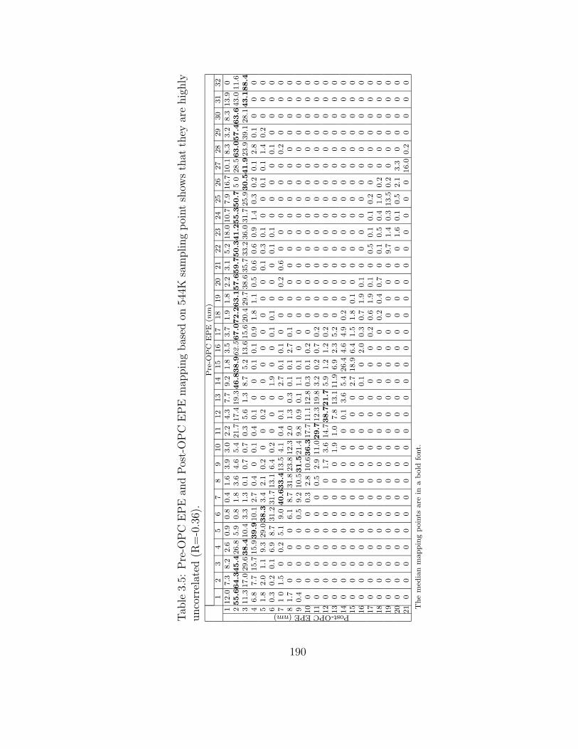
Tab
le3.
5:P
re-O
PC
EP
Ean
dPos
t-O
PC
EP
Em
appin
gbas
edon
544K
sam
pling
poi
nt
show
sth
atth
eyar
ehig
hly
unco
rrel
ated
(R=
-0.3
6).
Pre
-OP
CE
PE
(nm
)1
23
45
67
89
10
11
12
13
14
15
16
17
18
19
20
21
22
23
24
25
26
27
28
29
30
31
32
Post-OPCEPE(nm)
112.0
7.3
8.2
2.6
0.9
0.8
0.4
1.6
3.9
3.0
2.2
4.3
7.7
9.2
1.8
3.5
3.7
1.9
1.8
2.2
3.1
5.2
18.0
10.7
7.9
16.7
10.1
8.3
3.2
8.3
13.9
02
55.6
64.3
45.4
26.8
5.9
0.8
1.8
3.6
4.6
5.4
21.7
17.4
19.3
46.8
38.9
62.5
67.0
72.2
63.1
57.6
59.7
50.3
41.2
55.3
50.7
50
28.5
63.0
57.4
63.6
43.0
11.6
311.3
17.0
29.6
38.4
10.4
3.3
1.3
0.1
0.7
0.7
0.3
5.6
1.3
8.7
5.2
13.6
15.6
20.4
29.7
38.6
35.7
33.2
36.0
31.7
25.9
30.5
41.9
23.9
39.1
28.1
43.1
88.4
46.8
7.7
15.7
15.9
39.9
10.1
2.7
0.4
00.1
0.4
0.1
00
0.1
0.1
0.9
1.8
1.1
0.5
0.6
0.6
0.9
1.4
0.3
0.2
0.1
2.8
0.1
00
05
1.8
2.0
1.1
9.3
29.0
38.3
3.4
2.1
0.2
00
0.2
00
00
00
00
0.1
0.3
0.1
00
0.1
0.1
1.4
0.2
00
06
0.3
0.2
0.1
6.9
8.7
31.2
31.7
13.1
6.4
0.2
00
01.9
00
0.1
0.1
00
00.1
0.1
00
00
0.1
00
00
71
01.5
00.2
5.1
9.0
40.6
33.4
13.5
4.1
0.4
0.1
02.7
0.1
0.1
00
00.2
0.6
00
00
00
0.2
00
00
81.7
00
00
6.1
8.7
31.8
23.8
12.3
2.0
1.3
0.3
0.1
0.1
2.7
0.1
00
00
00
00
00
00
00
09
0.4
00
00
0.5
9.2
10.5
31.5
21.4
9.8
0.9
0.1
1.1
0.1
00
00
00
00
00
00
00
00
010
00
00
00
0.3
2.8
10.6
36.3
17.7
11.1
12.8
0.3
0.1
0.2
00
00
00
00
00
00
00
00
11
00
00
00
00.5
2.9
11.0
29.7
12.3
19.8
3.2
0.2
0.7
0.2
00
00
00
00
00
00
00
012
00
00
00
00
1.7
3.6
14.7
38.7
21.7
5.9
1.2
1.2
0.2
00
00
00
00
00
00
00
013
00
00
00
00
01.9
1.0
7.8
13.1
11.9
6.9
2.3
5.2
00
00
00
00
00
00
00
014
00
00
00
00
00
00.1
3.6
5.4
26.4
4.6
4.9
0.2
00
00
00
00
00
00
00
15
00
00
00
00
00
00
02.7
18.9
6.4
1.5
1.8
0.1
00
00
00
00
00
00
016
00
00
00
00
00
00
00.1
02.0
0.3
0.7
1.9
0.1
00
00
00
00
00
00
17
00
00
00
00
00
00
00
00
0.2
0.6
1.9
0.1
00.5
0.1
0.1
0.2
00
00
00
018
00
00
00
00
00
00
00
00
00.2
0.4
0.7
00.1
0.5
0.4
1.0
0.2
00
00
00
19
00
00
00
00
00
00
00
00
00
00
09.7
1.4
0.3
13.5
0.2
00
00
00
20
00
00
00
00
00
00
00
00
00
00
00
1.6
0.1
0.5
2.1
3.3
00
00
021
00
00
00
00
00
00
00
00
00
00
00
00
00
16.0
0.2
00
00
The
med
ian
mappin
gpoin
tsare
ina
bold
font.
190

un-OPCed design ranges from 1 to 32nm. Meanwhile, we perform OPC on the
same but OPCed design to get new EPEs for the 544K points, which ranges
from 1 to 21nm, as in the first column. Then, we compute the distribution of
corresponding post-OPC EPE values for each pre-OPC EPE as in Table 3.5 .
For example, a point with 32nm EPE before OPC may have 3nm EPE after
OPC with 88.4% probability. We also mark the largest probability for each
pre-OPC EPE in bold to show the trend.
For though comparison, we prepare a conventional grid-based detailed
router (DR) as well as a lithography aware ripup/rerouting like RADAR [154]
(RR). Instead of doing lithography simulation without OPC in [154], we ap-
ply OPC to RR as well for more accurate hotspot detection. Therefore, we
can have four different routers DR, DR+RR, ELIAD, and ELIAD+RR.
Fig. 3.33 illustrates these routing algorithms. Note that we use A* search to
find min-cost path in all the routers.
Table 3.6 comprehensively compares results from all the routers in
Fig. 3.33. It shows that ELIAD significantly improves overall EPE for both
designs. In terms of M1 hotspot (with 15nm EPE tolerance), ELIAD has 75%
Global Routing
Detailed Router
(DR)
Detailed Router (DR)
ELIAD
Calibre OPC/ORC for final verification
Calibre OPC/ORC
Fix Violations (RR)
ELIAD
Calibre OPC/ORC
Fix Violations (RR)
Figure 3.33: Experimental flow with four different routing algorithms [110].
191

Tab
le3.
6:C
ompar
ison
bet
wee
nva
riou
sro
ute
rson
two
indust
rial
des
igns.
EP
E(n
m)
Rat
iodes
ign
route
rw
irel
enru
nti
me
M1
M2
M1
M2
(mm
)(s
ec)
5–10
10–1
515+
5–10
10–1
515+
runti
me
hot
spot
ahot
spot
a
DR
6002
.450
9.9
1657
251
82285
7468
4304
90
14.
015
.0ck
t1D
R+
RR
[154
]60
08.0
8364
.3b
1359
245
49226
4831
2176
82
16.4
3.1
13.7
59.5
Kum
2E
LIA
D60
03.5
728.
619
8598
576
257
376
1.4
1.1
15.
6Knet
sE
LIA
D+
RR
a60
08.1
8969
.1b
1774
895
72
221
276
17.6
11
DR
1016
8.5
353.
617
124
5834
424
4082
2062
54
17.
627
.0ck
t2D
R+
RR
[154
]10
175.
172
60.5
b14
104
5127
394
2614
1385
49
20.5
7.0
24.5
50.2
Kum
2E
LIA
D10
169.
645
0.2
1318
1209
69
354
222
1.3
1.2
17.
9Knet
sE
LIA
D+
RR
1017
4.8
7456
.2b
1179
1125
56
331
180
21.1
1-
aE
PE
thre
shol
dfo
rlith
o-hot
spot
is15
nm
.b
RR
has
one
round
ofunav
oidab
leC
alib
re-O
PC
/OR
Cto
extr
act
lith
o-hot
spot
sw
hic
hta
kes
majo
rity
ofru
nti
me.
192

Tab
le3.
7:D
etai
led
EP
Ere
duct
ion
(%)
over
DR
com
par
ison
bet
wee
nD
R+
RR
and
ELIA
Dby
par
titi
on.
route
rD
R+
RR
[154
]E
LIA
Ddes
ign
ckt1
ckt2
ckt1
ckt2
laye
rM
1M
2M
1M
2M
1M
2M
1M
2E
PE
(nm
)5–
1010
+5–
1010
+5–
1010
+5–
1010
+5–
1010
+5–
1010
+5–
1010
+5–
1010
+
P1
31.4
30.5
13.5
49.3
14.5
14.4
36.1
36.6
82.1
73.2
91.7
98.9
92.9
77.9
90.4
100.
0P
221
.913
.133
.055
.712
.17.
337
.337
.082
.869
.890
.398
.891
.774
.590
.699
.1P
322
.817
.624
.546
.716
.711
.140
.231
.483
.574
.492
.498
.890
.079
.094
.099
.2P
411
.61.
935
.840
.332
.934
.344
.053
.892
.777
.784
.797
.090
.591
.484
.010
0.0
P5
9.6
8.5
37.8
41.5
18.6
17.8
16.7
16.0
95.4
88.6
99.1
98.8
90.4
76.9
92.3
99.5
P6
18.4
10.5
46.9
55.5
19.4
19.6
37.2
39.2
91.9
86.5
99.9
100.
088
.673
.591
.499
.5P
712
.720
.140
.851
.114
.422
.441
.341
.388
.285
.199
.998
.691
.881
.689
.097
.1P
89.
40.
010
.322
.48.
221
.737
.850
.085
.991
.199
.110
0.0
95.9
91.7
97.3
95.5
P9
9.1
19.2
43.6
51.8
19.8
20.5
37.9
38.0
93.1
87.2
99.5
99.1
94.4
86.5
90.8
99.5
P10
16.7
15.1
41.1
52.2
17.1
19.8
30.7
28.5
93.4
91.5
99.8
100.
093
.785
.492
.498
.2P
1116
.317
.749
.559
.023
.024
.346
.438
.683
.584
.799
.799
.795
.787
.491
.299
.1P
12-8
.310
.034
.958
.543
.448
.1-1
4.8
23.1
94.8
95.0
100.
010
0.0
94.6
86.4
88.9
100.
0av
g14
.313
.734
.348
.720
.021
.832
.636
.189
.083
.796
.399
.292
.582
.791
.098
.9st
d9.
78.
312
.410
.29,
610
.716
.710
.55.
18.
15.
20.
92.
46.
33.
21.
4co
v(
std
avg)
0.68
0.61
0.36
0.21
0.48
0.49
0.51
0.29
0.06
0.10
0.05
0.01
0.03
0.08
0.03
0.01
193
less than DR and 66% less than DR+RR for ckt1, and 84% less than DR
and DR+RR for ckt2. The reduction is even much more for M2 hotspot, at
least 93% and 96% for ckt1 and ckt2, respectively. When ELIAD combined
with RR (ELIAD+RR), it can further improve printability (about 10%). This
implies that ELIAD, a correct-by-construction approach is highly superior to
a post-optimization (RR) approach, but can be complementary with it (RR)
by providing an excellent starting point. Regarding runtime, while ELIAD is
at most 60% slower than DR, RR involves huge overhead mainly from hotspot
detection using expensive OPC/ORC. ELIAD is at least 10x faster than any
approach with RR (DR+RR and ELIAD+RR). Finally, there is negligible
difference among routers in terms of wirelength.
Table 3.7 further analyzes the performance of ELIAD by comparing
EPE reduction with DR+RR in a partition-by-partition manner. As expected,
ELIAD yields significantly better EPE reduction, but our point here is that
ELIAD can improve EPE globally, while DR+RR cannot. When we com-
pute the coefficient of variance (cov) of hotspot reduction over 12 partitions
(P1–P12) for ELIAD and DR+RR, ELIAD and DR+RR have 0.45 and 0.046
respectively. The implication of 10x smaller cov is that the performance of RR
highly depends on the complexity of initial routing and local congestion (e.g.,
hard to find a totally new routing path), as it cannot make radical changes to
improve printability. However, since ELIAD runs in a correct-by-construction
way from the scratch, it can consistently improve printability all over the place.
This situation can also be observed from the Fig. 6 in RADAR [154] where
194

most of hotspot removals are from the outer regions rather than the core.
3.5 Summary
We propose the first manufacturability aware routing framework where
three major challenges (topography variation [58], random defects [153], and
printability [60]) are addressed at global, track, and detailed routing respec-
tively according to the characteristics of the issue [174].
Fist, wire density should be a key metric for manufacturability and
timing optimization in nanometer design. We present the first wire density-
driven global routing to improve CMP variation and timing based on a predic-
tive CMP model and several novel techniques. Experimental results are highly
encouraging, showing that the proposed algorithm outperforms the state-of-
the-art congestion-driven global router, BoxRouter in terms of CMP variation
and timing with negligible overhead in wirelength, and even slightly better
routability.
Second, in order to cope with yield loss due to random defects in ad-
vanced technologies, we present TROY, an efficient yield-driven track router.
With effective wire ordering and wire sizing/spacing optimization based on
minimum Hamiltonian path and second order cone programming, experimen-
tal results show that TROY reduces yield loss significantly. As TROY finds
globally optimal wire sizing and spacing for a given wire order, it may be easily
modified for any wire sizing and spacing related optimization such as crosstalk
and timing [140].
195

Last, we present ELIAD, a lithography aware detailed router in a
correct-by-construction approach based on a fast yet high fidelity litho-metric
with OPC consideration. Experimental results shows that ELIAD is signifi-
cantly superior to a ripup/rerouting technique or a post-processing strategy,
only at small runtime overhead.
196

Chapter 4
Physical Synthesis for Emerging Technologies
In Chapter 2 and 3, we show that physical synthesis plays a crucial
role in design/manufacturing closure of a CMOS VLSI system based on a
traditional silicon fabrication process. Physical synthesis is expected to con-
tinue its role as a technology enabler for emerging technologies, and needs to
evolve according to natures in such technologies. In this chapter, we discuss
two new routing algorithms, one for double patterning technology and digital
microfluidic biochip design.
Double patterning technology (DPT) is a most likely lithography so-
lution for 32/22nm technology nodes as of 2008 due to the delay of Extreme
Ultra Violet lithography. However, it should hurdle two challenges before be-
ing introduced to mass production, layout decomposition and overlay error. In
Section 4.1, we present the first detailed routing algorithm for DPT to improve
layout decomposability and robustness against overlay error, by minimizing in-
decomposable wirelength and the number of stitches. We first show that layout
decomposition is significantly more complex than a 2-coloring problem, when
a feature can be splitted into multiple polygons. Next, we propose a path
coloring algorithm which decomposes a given routing path while minimizing
197

the number of stitches. Then, we propose a DPT-friendly detailed routing
algorithm which simultaneously finds a DPT-friendly routing path and corre-
sponding layout decomposition for each net. Experimental results show that
the proposed approach improves the quality of layout significantly in terms
of decomposability and the number of stitches with 3.6x speedup, compared
with a current industrial DPT design flow.
In Section 4.2, we propose a high-performance droplet router for digi-
tal microfluidic biochip (DMFB) design. Due to recent advancements in bio-
MEMS and its various applications to clinical, environmental, and military
operations, the design complexity and the scale of a DMFB are expected to
explode in near future, thus requiring strong support from CAD as in conven-
tional VLSI design. Among multiple design stages of a DMFB, droplet routing
which schedules the movement of each droplet in a time-multiplexed manner
is one of the most critical design challenges due to high complexity as well as
large impacts on performance. Our algorithm first routes a droplet with higher
bypassibility which less likely blocks the movement of the others. When mul-
tiple droplets form a deadlock, our algorithm resolves it by backing off some
droplets for concession. The final compaction step further enhances timing as
well as fault-tolerance by tuning each droplet movement greedily. Experimen-
tal results on hard benchmarks show that our algorithm achieves over 35x and
20x better routability with comparable timing and fault-tolerance than the
popular prioritized A* search [18] and the state-of-the-art network-flow based
algorithm [243], respectively.
198

4.1 Double Patterning Technology
As discussion in Chapter 3, the semiconductor industry is facing ever-
increasing manufacturing challenges, and in particular printability degradation
due to subwavelength lithography [44,45,60,110,129,154,232], as we discussed
in Section 3.4. To overcome such printability degradation, Extreme Ultra
Violet (EUV) lithography with 13.5nm wavelength has been researched and
developed as Next Generation Lithography for the last decade, targeting for
sub 45nm nodes. However, the deployment of EUV for commercial mass
production has been delayed multiple times (due to material issues, mask
fabrication, EUV system, and so on), and is likely to be pushed out to the
16nm node in 2013, if it ever materializes [73,119,132].
To bridge the gap between current single exposure immersion lithogra-
phy and EUV lithography, double patterning technology (DPT) receives large
attention from industry and is regarded as a technically and practically viable
alternative to achieve high resolution for 32/22nm nodes [13,111,117,132,178,
191,223]. The key idea of DPT is to decompose a single layout into two masks
in order to increase pitch size and improve depth of focus (DOF) [119, 195].
Fig. 4.1 illustrates the concept of DPT. The increased pitch size brings sev-
eral advantages which enable higher resolution and better printability [111].
More Sub Resolution Assist Features (SRAF) can be added in a relaxed pitch
area, and the impact of forbidden pitch is reduced. The performance of Op-
tical Proximity Correction (OPC) algorithms can be enhanced by avoiding
mask-fabrication-imposed constraints. DPT is generic to be applied for poly,
199

Mask 1
Mask 2
AB
C D E
Layout Decomposition
Figure 4.1: In DPT, one single layer can be decomposed into two masks toeffectively increase pitch size [13].
metal, active, and even via layers. Furthermore, current manufacturing in-
frastructures (e.g., stepper) and materials (e.g., photo-resist) can be reused
without expensive modification. These advantages all make DPT as the most
prominent manufacturing technology for 32/22nm nodes.
However, the deployment of DPT needs to tackle two major challenges,
layout decomposition and overlay error [13,73,119,195]. As shown in Fig. 4.1,
a layout has to be decomposed (or colored differently) into two masks. Two
adjacent features should be assigned to different masks or opposite colors, if
their spacing is less than minimum double patterning space. However, such de-
composition is not always feasible, especially for complex 2D patterns common
in metal layers [13,148,178]. For such indecomposable cases, a straightforward
solution may be to modify the layout or design, but this will be highly expen-
sive. Another solution is to split one polygon into two in order to resolve
decomposition conflicts, which will introduce a stitch as shown in Fig. 4.2 (a).
However, it is known that such a stitch is highly sensitive to overlay error, po-
200

Stitch
(a) A polygon can be splitted to resolvea decomposition or coloring conflict ata cost of stitch.
Stitch
(b) Stitch may result in signifi-cant printability degradation dueto overlay error and line-end effect.
Figure 4.2: The concept of a stitch is elaborated by an example in (a), and itssusceptibility to overlay error is demonstrated in (b).
tentially causing pinching or bridging issues as shown in Fig. 4.2 (b) [73,148].
Therefore, it is of great importance to make a layout more decomposable and
reduce the number of stitches.
Since DPT is relatively a new technology, there are only a few pre-
vious works on layout decomposition mainly from a mask synthesis perspec-
tive. Some commercial simulator is used to decompose a layout rigorously
in [117], and design guidelines for successful pattern decomposition are dis-
cussed in [223]. A fast pattern matching technique to decompose a layout is
proposed in [191]. All these works mainly focus on post-design optimization,
which may be too late for successful decomposition. Also, none of them min-
imize the number of stitches systematically. Therefore, it is in great demand
to take DPT into account during design time in order to generate a highly de-
201

composable layout with fewer stitches. Detailed routing can be a right stage
to address DPT challenges due to the following reasons: (a) most of hard-
to-decompose patterns are from complex 2D routing wires; (b) it is the last
major design optimization step with a comprehensive view on DPT; (c) there
is considerable design flexibility to find reasonable trade-off between DPT and
conventional design objectives (e.g., timing, via, wirelength).
In this section, we propose the first DPT-friendly detailed routing algo-
rithm. The key idea behind our algorithm is to perform detailed routing and
layout decomposition (or coloring) simultaneously in a correct-by-construction
manner to accomplish high layout decomposability and reduce the number of
overlay-error-prune stitches. Therefore, our DPT-friendly detailed routing di-
rectly outputs a decomposed layout without an extra time-consuming decom-
position step. Our experimental results are very promising.
The rest of the section is organized as follows. Section 4.1.1 provides
preliminaries on double patterning technology and its challenges, further mo-
tivates our work by discussing the complexity of layout decomposition and the
need of DPT consideration during design time. Then, we propose our DPT-
friendly detailed routing algorithm in Section 4.1.2. Experimental results are
discussed in Section 4.1.3.
4.1.1 Background and Definitions
In this subsection, we illustrate the complexity of layout decomposi-
tion in Section 4.1.1.4 after providing background on double patterning tech-
202

nology in Section 4.1.1.1, its challenges in Section 4.1.1.2, and definitions in
Section 4.1.1.3.
4.1.1.1 Double Patterning Technology (DPT)
The difficulty of a process technology can be described by k1 in Rayleigh
Formulae [25]:
k1 = HP NAλ
(4.1)
where λ is wavelength of the light (currently 193nm for ArF lithography),
NA is numerical aperture, and HP is minimum printable half-pitch. Note
that higher k1 implies easier manufacturing. If we need to print a feature
in the 32nm node with the current single exposure infrastructure, k1 would
be below 0.25, which is too low to have profitable yield. Therefore, we may
consider improving the infrastructure itself to increase k1, which can be accom-
plished in two ways. The first way is to increase NA with the 3rd generation
immersion fluid (Refraction Index (RI) > 1.8), enhanced photo-resist, and
larger lens. The other way is to use Extreme Ultra Violet (EUV) light source
(λ=13.5nm). However, neither way will be ready until 2013 [73]. Note that
although there are direct lithography techniques like as E-Beam lithography
and Nano-imprint, they are still highly premature and in the research state. In
light of these physical and practical limitations in the above two ways, the only
feasible solution is to increase pitch size without changing minimum feature
size, which is achieved by double patterning technology (DPT). By decompos-
ing a layout into two masks as shown in Fig. 4.1, we can effectively double HP ,
203

(a) Positive tone or double/dual line process for DPT.
(b) Negative tone or double/dual trench process for DPT.
Figure 4.3: In a DPT process, one single layer is decomposed into two masks,and it requires two exposures and two etching [178].
theoretically enabling 65nm technology/infrastructure to print 32nm designs.
As expected, however, DPT process is highly complex, as one layer
needs to be patterned by two exposures and two etching with two masks. There
are several DPT lithography processes; litho1-etch1-litho2-etch2 (LELE) [73],
spacer type DPT [20], and litho oriented DPT [209]. Fig. 4.3 shows two popular
LELE DPT processes, the positive tone process in (a) and the negative tone
process in (b). To get the final wafer image, each mask is projected separately
and each lithography image is superposed through each process step in both
approaches.
In a positive process shown in Fig. 4.3 (a), it requires bright-field masks
and double line patterning. The first mask is exposed and then etch-trimmed,
which is followed by the second litho and etch processes. It requires a hard
204

mask (HM) layer in order to protect the first exposure patterns from possible
pattern damages during the second patterning step. Meanwhile, a negative
process in Fig. 4.3 (b) requires dark-field masks and double trench patterning
in order to improve the lithographic process window. In both processes, the
first litho and etch through the bottom anti-reflection coating (BARC) opening
and HM-etch lead to a set of trenches which are different from the intended
patterns. However, after the second litho and etch (through the BARC and
HM-etch again), we accomplish the intended patterns as shown in the last
steps of Fig. 4.3 (a) and (b).
Even though there can be some differences in different DPT processes,
all DPT processes are highly complex and involve multiple common challenges
in both design and manufacturing sides such as layout decomposition and
stitch minimization, which will be discussed in Section 4.1.1.2.
4.1.1.2 Challenges in DPT
The two most important issues to deal with DPT are layout decompo-
sition and overlay-error-prune stitches [148].
Layout Decomposition in DPT is to decompose (color) the original design
polygons into two groups or colors (BLACK or GRAY) to decide which
polygon will be placed on which mask. Currently known decomposition
approaches involve tedious manual procedures [191]. Such decomposi-
tion should be done under the minimum double patterning spacing con-
straint, which is imposed between two polygons on the same mask or
205

color. If there is any violation or conflict, it should resolved either by
splitting a polygon into multiple polygons at a cost of stitches or altering
a layout/design itself.
Stitch Minimization is another critical issue in DPT due to the overlay er-
ror which is caused by the mismatch between the first patterning and
the second patterning. Since the corner of the DPT overlay error distri-
bution (e.g., −3σ) is over 5nm on 40nm half pitch NAND flash (memory
logic) [12], a typical overlay error will be much more serious on sub 32nm
random logic designs. Unfortunately, a stitch is known to be highly sen-
sitive to the overlay error, causing bridging or pinching. Fig. 4.2 (b)
shows the example of a notching error due to a stitch.
Due to such criticality and importance, layout decomposition and stitch min-
imization have been considered during mask synthesis/manufacturing [117,
191, 223], but cannot be effectively addressed due to their high design depen-
dency. Therefore, we propose to take DPT into account during design time to
generate a more DPT-friendly layout.
4.1.1.3 Definitions
We explain some key definitions in DPT with Fig. 4.4: mindp, BLACK-
colorable, GREY-colorable, and BI-colorable. During layout decomposition,
as mentioned earlier, polygons will be divided into two masks or two colors
(GREY or BLACK). And, two polygons on the same mask (thus in the same
206
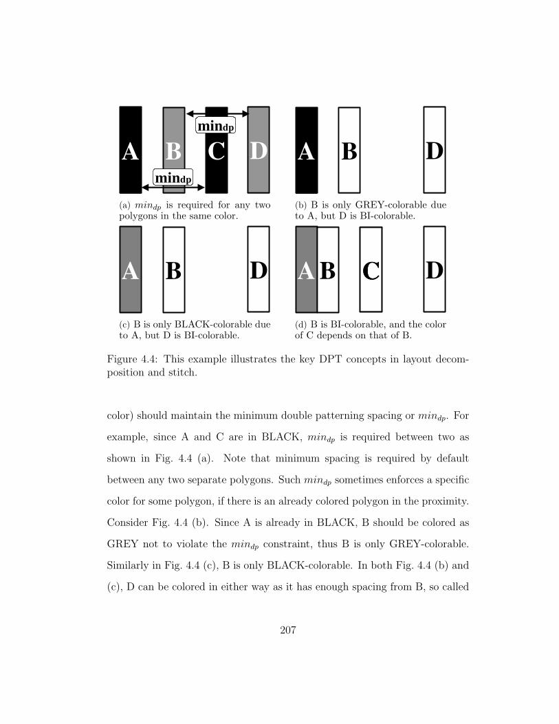
AA BB CC DDmindp
mindp
(a) mindp is required for any twopolygons in the same color.
AA BB DD
(b) B is only GREY-colorable dueto A, but D is BI-colorable.
AA BB DD
(c) B is only BLACK-colorable dueto A, but D is BI-colorable.
AA DDBB CC
(d) B is BI-colorable, and the colorof C depends on that of B.
Figure 4.4: This example illustrates the key DPT concepts in layout decom-position and stitch.
color) should maintain the minimum double patterning spacing or mindp. For
example, since A and C are in BLACK, mindp is required between two as
shown in Fig. 4.4 (a). Note that minimum spacing is required by default
between any two separate polygons. Such mindp sometimes enforces a specific
color for some polygon, if there is an already colored polygon in the proximity.
Consider Fig. 4.4 (b). Since A is already in BLACK, B should be colored as
GREY not to violate the mindp constraint, thus B is only GREY-colorable.
Similarly in Fig. 4.4 (c), B is only BLACK-colorable. In both Fig. 4.4 (b) and
(c), D can be colored in either way as it has enough spacing from B, so called
207

BI-colorable.
An interesting case is in Fig. 4.4 (d) where A and B are abutted. For
this case, B is BI-colorable, because coloring B as GREY does not violate
the mindp constraint (as, A and B can be treated as one bigger polygon)
and coloring B as BLACK is still fine at a cost of a stitch. The color of C
depends on how B will be colored. If B is in GREY eventually, then C will be
BLACK-colorable (otherwise GREY-colorable).
4.1.1.4 Complexity of Layout Decomposition
At the first glance, layout decomposition for DPT seems identical to
the phase-assignment problem [21], as both can be formulated as a 2-coloring
problem. However, there are two key differences. Phase-assignment is for
the space between polygons, but layout decomposition for DPT is for the
polygons. More importantly, resolving a conflict in phase-assignment needs to
involve layout modification (e.g., increasing spacing) [21], but not necessarily
in layout decomposition for DPT, as a polygon can be severed into multiple
polygons in DPT (which does not change the layout).
Consider a layout in Fig. 4.5 (a) where five disconnected polygons are
shown along with five conflicts in double-headed arrows. We can formulate
layout decomposition of Fig. 4.5 (a) as a 2-coloring problem by building a
corresponding conflict graph and performing 2-coloring (BLACK or GRAY)
based on Chatin’s algorithm [40]. In Fig. 4.5 (b), a conflict graph for the
layout in (a) is constructed and a double-ended queue for coloring is prepared.
208

AB
CD
E
(a)
An
exam
ple
for
layout
de-
com
posi
tion
for
DP
Tis
show
n
with
five
conflic
tsam
ong
poly
-
gons.
A
BCD
E
(b)
Aco
nflic
tgra
ph
for
2-c
olo
ring
can
be
built
from
(a)
with
a
double
-ended
queu
e.
A
BCDE
(c)
The
node
Ew
ith
deg
ree<
2is
det
ach
ed
and
push
edin
toth
eto
p
ofth
equeu
e.
A
BC
D E
(d)
The
node
Dw
ith
deg
ree<
2is
det
ach
ed
and
push
edin
toth
eto
p
ofth
equeu
e.
AB
CED
(e)
The
node
Aw
ith
the
larg
est
deg
ree
isde-
tach
edand
put
into
the
bott
om
ofth
equeu
e.
A
BCD
E
ABC ED
(f)
The
node
Con
the
top
of
the
queu
eis
col-
ore
das
BLA
CK
and
popped
out.
A
BCD
E
AB ED
(g)
The
node
Bon
the
top
of
the
queu
eis
colo
red
as
GR
AY
and
popped
out.
A
BCD
E
AE
(h)
The
node
Eon
the
top
of
the
queu
eis
col-
ore
das
BLA
CK
and
popped
out.
A
BCD
E
A(i
)T
he
node
Aon
the
top
ofth
equeu
eca
nnot
be
colo
red
due
toth
e
conflic
tsw
ith
Band
C.
AB
CD
EStitc
h
(j)
How
ever
,th
enode
Aca
nbe
colo
red
with
BLA
CK
and
GR
AY
with
ast
itch
,re
sultin
gin
succ
ess-
fuldec
om
posi
tion
for
DP
T.
A
CED B
(k)
The
node
Bw
ith
the
larg
est
deg
ree
isde-
tach
edand
put
into
the
bott
om
ofth
equeu
e.
A
BCD
E
BAC ED
(l)
The
node
Con
the
top
of
the
queu
eis
col-
ore
das
BLA
CK
and
popped
out.
A
BCD
E
BE
(m)
The
node
Eon
the
top
of
the
queu
eis
colo
red
as
BLA
CK
and
popped
out.
A
BCD
E
B(n
)T
he
node
Bon
the
top
ofth
equeu
eca
nnot
be
colo
red
due
toco
n-
flic
ts.
AB
CD
EUncolorab
le
(o)
The
node
Bca
nnot
be
col-
ore
ddue
toA
inG
RA
Yand
Cin
BLA
CK
,re
sultin
gin
dec
om
posi
-
tion
failure
.
Fig
ure
4.5:
This
exam
ple
des
crib
esa
layo
ut
dec
ompos
itio
nan
dsh
ows
that
layo
ut
dec
ompos
itio
nw
ith
stit
chfo
rD
PT
ism
ore
com
ple
xth
anphas
e-as
sign
men
tw
hic
his
equiv
alen
tto
2-co
lori
ng
[122
].
209

As in Chatin’s algorithm, a node with degree <2 is repeatedly detached from
the graph and pushed into the top of the queue. In Fig. 4.5 (c), the node E is
detached, which successively reduces the degree of the node D to 1, resulting
in Fig. 4.5 (d). Since there is no node with degree 1 in Fig. 4.5 (d), we decide
to spill the node A, thus insert to the bottom of the queue as in Fig. 4.5 (e).
Then, as both B and C have degree 1, we can push B, and then C into the
queue sequentially.
Once all the nodes are stored in the queue, we can pop out one node
from the top of the queue at a time for coloring. As shown in Fig. 4.5 (f),
we pop out C and color it as BLACK. Next, we can pop out B and color
it as GRAY not to conflict with C as in Fig. 4.5 (g). After several steps
including Fig. 4.5 (h), we encounter the situation in Fig. 4.5 (i) where A cannot
be colored due to the conflicts with B and C. In a 2-coloring problem, such
situation implies this graph is uncolorable, which requires layout modification
in phase-assignment [122], but not necessarily in DPT. As in Fig. 4.5 (j), layout
decomposition can be completed by splitting the polygon A into two parts at
a cost of stitch on A.
Let us also consider the result of not selecting A in Fig. 4.5 (e). Al-
though we decide to spill the node B instead of A as shown in Fig. 4.5 (k), it is
still impossible to make the graph 2-colorable as in Fig. 4.5 (n). However, this
will make the layout indecomposable as shown in Fig. 4.5 (o). As a result, the
fact that a conflict graph is not 2-colorable does not guarantee the infeasibility
of layout decomposition for the corresponding layout, because some conflicts
210

can be resolved by stitches, leading to Theorem 4.1.1.
Theorem 4.1.1. Let G be the conflict graph of a layout L. Then, finding a
2-coloring solution of G is not equivalent to layout decomposition of L when a
polygon can be severed into multiple polygons with stitches.
Further, the complexity of finding a layout decomposition solution with
the minimum number of stitches is unknown yet, but we predict it would be
NP-hard, as there are a number of places for stitches.
4.1.2 DPT-Friendly Detailed Routing
In this subsection, we propose our DPT-friendly detailed routing al-
gorithm. As a first step, we motivate DPT-friendly detailed routing in Sec-
tion 4.1.2.1. Then, we propose a routing path coloring algorithm to minimize
the number of stitches in Section 4.1.2.2, which provides two key observations
for DPT-friendly detailed routing in Section 4.1.2.3.
4.1.2.1 DPT Consideration during Design
Layout decomposition is the most critical step for DPT, as discussed in
Section 4.1.1.4, especially highly complex for metal layers due to 2D patterns
(while the poly layer has 1D patterns mostly). However, layout decomposition
itself can be very complex and cannot be solved by a 2-coloring algorithm as
discussed in Section 4.1.1.4, which clearly requires design time consideration,
more specifically during detailed routing. Current industrial effort to accom-
plish layout decomposition is to first finish detailed routing, and then perform
211
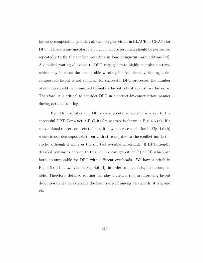
layout decomposition (coloring all the polygons either in BLACK or GRAY) for
DPT. If there is any uncolorable polygon, ripup/rerouting should be performed
repeatedly to fix the conflict, resulting in long design-turn-around-time [73].
A detailed routing oblivious to DPT may generate highly complex patterns
which may increase the uncolorable wirelength. Additionally, finding a de-
composable layout is not sufficient for successful DPT processes; the number
of stitches should be minimized to make a layout robust against overlay error.
Therefore, it is critical to consider DPT in a correct-by-construction manner
during detailed routing.
Fig. 4.6 motivates why DPT-friendly detailed routing is a key to the
successful DPT. For a net A-B-C, its Steiner tree is shown in Fig. 4.6 (a). If a
conventional router connects this net, it may generate a solution in Fig. 4.6 (b)
which is not decomposable (even with stitches) due to the conflict inside the
circle, although it achieves the shortest possible wirelength. If DPT-friendly
detailed routing is applied to this net, we can get either (c) or (d) which are
both decomposable for DPT with different overheads. We have a stitch in
Fig. 4.6 (c) but two vias in Fig. 4.6 (d), in order to make a layout decompos-
able. Therefore, detailed routing can play a critical role in improving layout
decomposability by exploring the best trade-off among wirelength, stitch, and
via.
212

A
B
C
(a) Net A-B-C and its Steiner tree withWL=21 in the dotted line are shown.The checked boxes are the blockages onM1.
B
C DecompositionConflict
A
(b) A routing solution from a conven-tional detailed router has WL=24, butwith decomposition conflicts inside thedotted circle.
B
Stitch
C
A
(c) One DPT-friendly solution is shownwith one stitch and WL=34.
M1 Wire B
M2 WireM2
Blockage
A
C
(d) Another DPT-friendly solution isshown without any stitch and WL=28,but with 2 vias.
Figure 4.6: This example motivates DPT consideration during detailed rout-ing. Detailed routing algorithm can make effective trade-off among layoutdecomposability, wirelength, the number of stitches, and the number of vias.
213
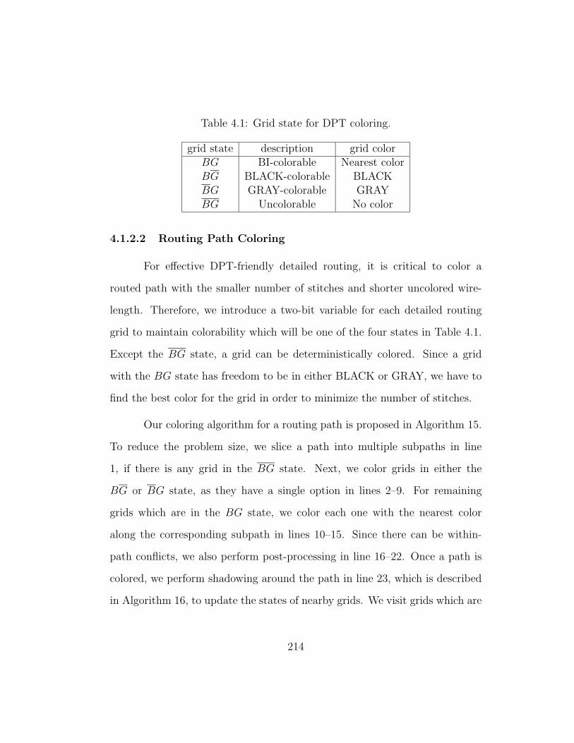
Table 4.1: Grid state for DPT coloring.
grid state description grid colorBG BI-colorable Nearest colorBG BLACK-colorable BLACKBG GRAY-colorable GRAYBG Uncolorable No color
4.1.2.2 Routing Path Coloring
For effective DPT-friendly detailed routing, it is critical to color a
routed path with the smaller number of stitches and shorter uncolored wire-
length. Therefore, we introduce a two-bit variable for each detailed routing
grid to maintain colorability which will be one of the four states in Table 4.1.
Except the BG state, a grid can be deterministically colored. Since a grid
with the BG state has freedom to be in either BLACK or GRAY, we have to
find the best color for the grid in order to minimize the number of stitches.
Our coloring algorithm for a routing path is proposed in Algorithm 15.
To reduce the problem size, we slice a path into multiple subpaths in line
1, if there is any grid in the BG state. Next, we color grids in either the
BG or BG state, as they have a single option in lines 2–9. For remaining
grids which are in the BG state, we color each one with the nearest color
along the corresponding subpath in lines 10–15. Since there can be within-
path conflicts, we also perform post-processing in line 16–22. Once a path is
colored, we perform shadowing around the path in line 23, which is described
in Algorithm 16, to update the states of nearby grids. We visit grids which are
214

Algorithm 15 Coloring Path
Input: a path p1: split p into a set of colorable subpaths by the BG state2: for each path t ∈ S do3: for each ordered grid d ∈ t do4: if d.state == BG then5: Color d as GRAY6: else if d.state == BG then7: Color d as BLACK8: end if9: end for
10: for each ordered grid d ∈ t do11: if d.state == BG then12: Color d with the nearest color13: end if14: end for15: end for16: for each ordered grid d ∈ p do17: for each grid x whose distance from d < mindp do18: if d.state == x.state and both colored and any uncolored grid or
stitch exists between d and x then19: Uncolor x20: end if21: end for22: end for23: Color Shadow(p)
within mindp distance from the path in order to update their states properly.
For example, grids near the BLACK one will have either the BG or BG state
not to violate the mindp spacing constraint as in lines 4–9 in Algorithm 16.
Assume that a routing path with 14 uncolored grids at various states
as shown in Fig. 4.7 (a). We begin by splitting the path into three subpaths,
X, Y, and Z, pivoting grids in the BG state, as in line 1 of Algorithm 15.
215

BG
BG BGBG BGBG
BG
BGBGBG BG BGBG BGBG BG
BG BG BGBG BG BG BG
BG BG BG BG BG
BG BG BG
subpath X subpath Y subpath Z
BGBG BG BGBG BG BG BG BG BG BGBG BG(a) This example shows how to color a set of grids in a routing path using Algo-rithm 15.
BGBGBGBG
BG
BGBG
BGBG BGBG
BGBG
(b) This example hasa potential conflictwithin a path.
BG BGBG BGBG
BGBG
BGBGBGBG BG
Conflict
(c) A simple coloringresults in a conflictaround the jog.
BGBG
BGBG BGBG
BGBG
BG
BGBG BGBG
(d) Some grids becomeuncolored to resolvethe conflict.
BGBG BGBGBGBG BGBG BGBG BGBG BGBG BGBG BGBG BGBG BGBG BGBG BGBG BGBG
BGBGBGBG BGBG BGBG BGBG BGBG BGBG BGBG BGBG BGBG BGBG BGBG BGBGBGBG
BGBG
BGBG
BGBG
BGBG
BGBG
BGBG
BGBG
BGBG
BGBG
BGBG
Minimum spacing
Minimum spacing
BGBG BGBG
BGBG BGBG
(e) Once the routing path is color, neighboring grids need to be shadowed byAlgorithm 16.
Figure 4.7: A routing path can be efficiently colored while minimizing thenumber of stitches, and its neighboring grids are shadowed for remaining un-routed/uncolored nets.
216

Algorithm 16 Color Shadow
Input: A path p1: for each ordered grid d ∈ p do2: for each grid x whose distance from d < mindp do3: if x /∈ p then4: if d is in BLACK then5: if x.state == BG then6: x.state == BG7: else if x.state == BG then8: x.state == BG9: end if
10: else if d is in GRAY then11: if x.state == BG then12: x.state == BG13: else if x.state == BG then14: x.state == BG15: end if16: end if17: end if18: end for19: end for
For each subpath, we first color grids in the BG or BG state. Then, we color
remaining grids in the BG state, by identifying the nearest color within the
same subpath, as shown by the arrows in Fig. 4.7 (a). In case a subpath
consist of only grids in the BG state like subpath Z, we color them all in one
random color (e.g., we randomly pick BLACK for them). Finally, we assemble
subpaths and grids in the BG state into one colored path.
For some case, there can be conflicts within a path. Consider the
example in Fig. 4.7 (c) where there is a jog. If we color the path in Fig. 4.7
(b) as done in Fig. 4.7 (a), we will have Fig. 4.7 (c) where there is a conflict.
217

Therefore, as the routing path is given and fixed, we need to detect the conflict
and further resolve it by uncoloring some grids in GRAY as shown in Fig. 4.7
(d), which is done in lines 16–22 of Algorithm 15. Fig. 4.7 (e) shows the states
of nearby grids after color shadowing. Note that a grid which is close to both
BLACK and GREY becomes in the BG state.
We can make two observations with the example in Fig. 4.7, which
results in Theorem 4.1.2 and 4.1.3, further leading to the idea of DPT-friendly
routing algorithm in Section 4.1.2.3.
Theorem 4.1.2. A routing path having a grid in the BG state will result in
layout decomposition failure.
Theorem 4.1.3. A routing path having two grids in the BG and BG states
adjacent will result in a stitch.
4.1.2.3 Detailed Routing Algorithm
According to the observations in Section 4.1.2.2, we will penalize three
cases in Table 4.2 during detailed routing. In detail, whenever a routing path
has a stitch due to the case 1 and 2, the penalty will be α. Also, in case a
Table 4.2: Lookup table for DPT routing.
case current grid state next grid state penalty
1 BG BG α (stitch)2 BG BG α (stitch)3 any state BG β (uncolorable)
218

Algorithm 17 DPT-Friendly Detailed Routing
Input: A set of blockages B, a set of nets N1: layout decomposition and color shadowing of B2: for each net n ∈ N do3: s = source grid of n4: t = target grid of n5: A priority queue Q = s6: while Q is not empty do7: x = dequeue from Q8: if x==t then9: break
10: end if11: for each adjacent grid d of x do12: cost = x.cost + 1 + A∗cost //unit wirelength is 113: if x.state==BG and d.state==BG then14: cost+ = α //to discourage a stitch15: else if x.state==BG and d.state==BG then16: cost+ = α //to discourage a stitch17: else if d.state==BG then18: cost+ = β //to reduce uncolorable wirelength19: end if20: if x and d not on the same layer then21: cost+ = γ //to discourage too many vias22: end if23: if d.cost > cost then24: d.cost = cost25: d.prev = x26: enqueue d to Q27: end if28: end for29: end while30: p = Backtrace from x to s of n31: Coloring Path(p)32: end for
219

routing path passes on a grid in the BG state, the penalty will be β as in
the case 3. We incorporate our observations into the proposed DPT-friendly
detailed routing as shown in Algorithm 17.
In line 1, we perform layout decomposition for existing routing block-
ages (e.g., pins, power/ground, clock, and so on) using Chatin’s algorithm [40]
as done in Section 4.1.1. When we need to spill a node, we pick one corre-
sponding to the largest polygon. Next, we perform color shadowing around
the colored blockages to guide detailed routing. Then, we perform a typical
detailed routing algorithm based on A* search as found in line 12. However,
to find a DPT-friendly path, we have additional cost modification from lines
13 to 22. From lines 13–16, we add α penalty to the routing cost to discourage
stitches from the case 1 and 2. And, in line 18, we also increase the routing
cost by β (≫ α) to minimize the number of uncolored grids. In line 21, we
can see one more penalty term γ which is to minimize the number of vias. As
discussed in Section 4.1.2.1, decomposability or stitch count can be improved
at a cost of via. Therefore, we also need to discourage dropping a via with γ.
Once the minimum cost routing path for a net is computed, we can color the
path using Algorithm 15.
4.1.3 Experimental Results
We implement our DPT-friendly routing in C++ and test on Intel
QuadCore 3.0 GHz Linux machine with 16G RAM. As benchmark designs, we
scale down four industrial 65nm ASIC designs to the 32nm technology node.
220
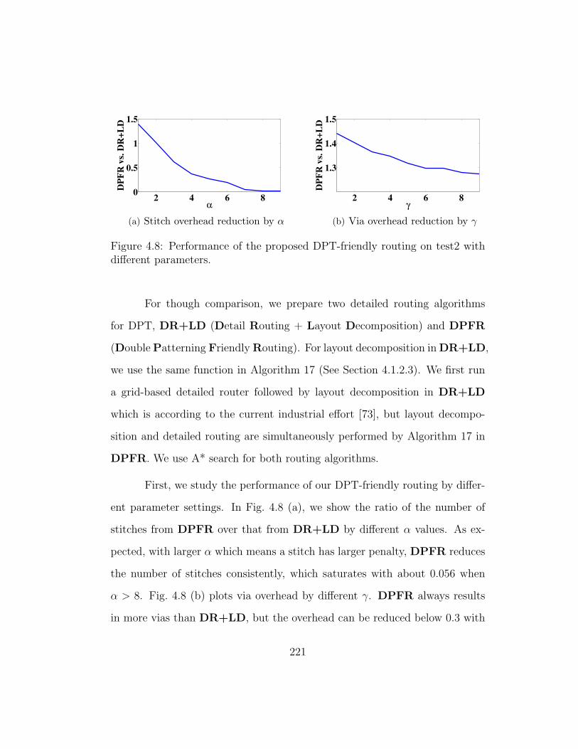
2 4 6 80
0.5
1
1.5
α
DP
FR
vs.
DR
+L
D
(a) Stitch overhead reduction by α
2 4 6 8
1.3
1.4
1.5
γ
DP
FR
vs.
DR
+L
D
(b) Via overhead reduction by γ
Figure 4.8: Performance of the proposed DPT-friendly routing on test2 withdifferent parameters.
For though comparison, we prepare two detailed routing algorithms
for DPT, DR+LD (Detail Routing + Layout Decomposition) and DPFR
(Double Patterning Friendly Routing). For layout decomposition in DR+LD,
we use the same function in Algorithm 17 (See Section 4.1.2.3). We first run
a grid-based detailed router followed by layout decomposition in DR+LD
which is according to the current industrial effort [73], but layout decompo-
sition and detailed routing are simultaneously performed by Algorithm 17 in
DPFR. We use A* search for both routing algorithms.
First, we study the performance of our DPT-friendly routing by differ-
ent parameter settings. In Fig. 4.8 (a), we show the ratio of the number of
stitches from DPFR over that from DR+LD by different α values. As ex-
pected, with larger α which means a stitch has larger penalty, DPFR reduces
the number of stitches consistently, which saturates with about 0.056 when
α > 8. Fig. 4.8 (b) plots via overhead by different γ. DPFR always results
in more vias than DR+LD, but the overhead can be reduced below 0.3 with
221

Tab
le4.
3:Per
form
ance
ofth
epro
pos
edD
PT
-fri
endly
det
aile
dro
uti
ng
algo
rith
m.
des
ignnet
sar
earo
ute
rw
irel
en(m
m)
via
runti
me
(sec
)dou
ble
pat
tern
ing
Rat
io(u
m2)
M1
M2
sum
M1-
M2ro
ute
rdec
ompos
itio
nsu
mst
itch
a fai
lure
(um
)bvia
runti
mest
itch
test
16K
15K
DR
+LD
1.97
8.7
10.6
189
91.7
1099
.611
91.3
109
7.75
13.
2721
.8D
PFR
1.98
8.7
10.7
216
364.
60
364.
65
0.15
1.14
11
test
26K
15K
DR
+LD
4.64
11.5
16.1
424
123.
696
6.5
1090
.115
911
.90
12.
7526
.5D
PFR
4.66
11.6
16.2
546
397.
10
397.
16
0.05
1.29
11
test
38K
12K
DR
+LD
0.54
10.2
10.8
5712
0.2
1517
.116
97.3
9210
.60
14.
3392
DP
FR
0.54
10.2
10.8
5939
2.9
039
2.9
10
1.04
11
test
48K
12K
DR
+LD
0.86
14.5
15.4
141
159.
014
94.7
1653
.716
934
.60
13.
8518
.8D
PFR
0.86
14.5
15.4
143
429.
90
429.
99
01.
011
1a
The
num
ber
ofst
itch
es.
bT
he
unco
lore
dw
irel
engt
hdue
toir
reso
lvab
leco
nflic
ts.
222

larger γ values.
Based on the results in Fig. 4.8, We compare DPFR and DR+LD on
four test designs with α = 9, β >> 10, and γ = 6 as shown in Table 4.3, which
demonstrates the effectiveness of DPFR, a simultaneous layout decomposition
and detailed routing for DPT. With negligible overhead in wirelength, we can
improve the quality of layouts in terms of double patterning; the number of
stitches for every design is reduced by at least 18x and up to 92x, and the
uncolorable wirelength is at most 0.15µm while DR+LD has at best 7.75µm.
Note that the uncolorable wirelength from DPFR is due to DPT-oblivious
pin locations. Via overhead is 12% on average. Even though DPFR is slower
than the routing portion of DR+LD, DPFR is about 3x faster considering
the overall flow. It is mainly because DR+LD has to work on a larger conflict
graph from the final layout for layout decomposition.
4.2 Digital Microfluidic Biochips
Since 1988, nearly 30 years after Dr. Feynman’s celebrated 1959 lec-
ture on future nanotechnology (presented to the American Physical Soci-
ety) [76], microelectromechanical system (MEMS) has significantly advanced
from the early stage of microfabrication/device research to the mature stage
of mass production for commercial applications, and now further opens up a
new era for exploring research and applications such as RF/optical commu-
nications, micro-energy fuel cells, or clinical/biochemical instruments [128].
Among them, bio-MEMS for clinical or biochemical purposes holds great
223

promise due to its cost effectiveness, portability, yet critical applications.
For example, a biochip based on bio-MEMS technology becomes popular
in analysis of DNA/protein for clinical/medical diagnosis, detection of tox-
ins/pathogens/terror for military/environmental safety, manipulation of bio-
logical samples for lab-experiments, and so on [62, 197]. Besides, all these
critical tasks can be performed in a small space efficiently without involving
any human experimenter or expensive equipment due to automated operations
at low cost.
One of the most advanced technologies to build a biochip is based on
microfluidics where micro/nano-liter droplets are controlled or manipulated
to perform intended biochemical operations on a miniaturized lab, so called
lab-on-a-chip (LOC) [160]. The old generation of microfluidic biochip consists
of several micrometer scale components including channels, valves, actuators,
sensors, pumps, and so on. Even though this generation shows successful ap-
plications like DNA probing, it is unsuitable to build a large and complex
biochip, because it uses continuous liquid flows, as like continues voltages in
analog VLSI design (See Section 4.2.1.1 for more details). The new generation
of microfluidic biochip has been proposed based on a recent technology break-
through where the continuous liquid flow is sliced or digitized into droplets.
Such droplets are manipulated independently by electric signals. This new
generation is referred to as a digital microfluidic biochip (DMFB).
Due to such a digital nature of a DMFB, any operation on droplets
can be accomplished with a set of library operations like VLSI standard li-
224

brary, controlling a droplet by applying a sequence of preprogrammed electric
signals [61]. Therefore, a hierarchical cell-based design methodology can be
applied to a DMFB. Under this circumstance, we can easily envision that a
large scale complex DMFB can be designed as done in VLSI, and market will
greatly demand such a DMFB due to economical/portable efficiency as well
as safety/health-critical applications. Hence, it is expected that DMFB design
needs CAD support as strongly as VLSI design shortly.
However, CAD research for DMFB design has started very recently.
In [199], the first top down methodology for a DMFB is proposed, which mainly
consists of architecture-level synthesis and geometry-level synthesis. Opera-
tion scheduling and resource binding are performed to minimize the maximum
chip response time in architecture-level synthesis (i.e., high-level synthesis in
VLSI design), while resources are physically placed as modules and operations
are connected by moving droplets in geometry-level synthesis (i.e., physical
synthesis in VLSI design). In detail, geometry-level synthesis can be further
divided into module placement and droplet routing. During module placement,
the location and time interval of each module are determined to minimize area
or chip response time. Since different modules can be on the same spot during
different time intervals based on reconfigurability (See Section 4.2.1.1), mod-
ule placement is equivalent to a 3D packing problem [201,242]. Meanwhile, in
droplet routing, the path of each droplet is found to transport it without any
unexpected mixture under design requirements. Similarly to module place-
ment, a spot can be used to transport different droplets during different time
225

intervals (simply in a time-multiplexed manner), which increases the complex-
ity of routing. The most critical goal of droplet routing is routability as in
VLSI [18], while satisfying timing constraint and maximizing fault-tolerance.
More discussion on prior papers to achieve this goal is in Section 4.2.1.2.
In this section, we propose a high-performance droplet router for a
digital microfluidic biochip (DMFB). Our approach is mainly based on two
ideas, bypassibility and concession. Bypassibility analysis quantifies how easy
for unrouted droplets to bypass blockages introduced by a routed droplet (the
easier to bypass, the higher bypassibility is). Therefore, we repeat routing one
with higher bypassibility to maximize the number of droplets routed, which
eventually leaves only the hard-to-route droplets under a deadlock situation.
Then, we break the deadlock by concession which backs off some droplets to
allow the others to pass by. These two ideas provide higher quality solutions
than [18,243]. The major contributions of this section include the following.
• We propose a simple yet effective metric, bypassibility to estimate the
degradation of routability after a droplet is routed. This maximizes the
number of routed droplets, and narrows down the problem size until
multiple droplets under a deadlock are identified.
• We introduce the concept of a concession zone where some droplet may
migrate to break a deadlock between droplets. We route earlier a droplet
with longer distance to any of concession zones, as it is harder to be
routed in a later stage of routing.
226

• We propose 2D routing for the droplet chosen by bypassibility analysis
to reduce runtime. If only one droplet chosen by bypassibility is routed
while the others are frozen, this can be solved in a compact 2D plane
rather than in a huge 3D plane where the third axis represents time.
The rest of this section is organized as follows. Section 4.2.1 presents
preliminaries. Especially, routing problems in a DMFB and a VLSI circuit
are compared to help readers with VLSI background, and further the droplet
routing problem in a DMFB is defined in Section 4.2.1.2. Section 4.2.2 presents
our proposed algorithm for DMFB routing. Experimental results are discussed
in Section 4.2.3.
4.2.1 Background and Problem Formulation
4.2.1.1 Digital Microfluidic Biochip
The first generation of biochips is based on a continuous-flow sys-
tem where liquid flows through microfabricated channels continuously using
electrokinetic-based micro-actuators. Although a continuous-flow biochip is
widely used for simple yet well-defined biochemical operations like DNA prob-
ing, it is inherently unsuitable for large scale complex biochip design due to
the following reasons: (a) permanently microfabricated channels limit the re-
configurability for both applications and fault-tolerance, (b) inevitable shear
flow around micro-actuators and diffusion on channels increase the possibility
of sample contamination [201].
To overcome the above drawbacks, a digital microfluidic biochip (DMFB)
227

is devised where liquid is discretized or digitized into independently control-
lable droplets (≪ 1µl), and each droplet is moved or manipulated on a sub-
strate according to a preprogrammed schedule. Such digitization and pro-
grammability enable to design a large scale and complex DMFB by allowing
a hierarchical and cell-based design methodology as in modern VLSI design.
They also provide reconfigurability for various biochemical applications with
enhanced fault-tolerance.
Although multiple technologies to control droplet such as chemical [78,
113], thermal [192] methods have been proposed, electrical methods such as
dielectrophoresis (DEP) [118] and electrowetting-on-dielectric (EWOD) [61,
182] have received more attention due to their high accuracy. Both techniques
leverage electrohydrodynamics for faster droplet movement, but DEP suffers
from excessive Joule heating [118]. In this work, we mainly consider a EWOD-
based DMFB, but the proposed algorithm itself is generic enough for any type
of technology.
Fig. 4.9 shows the schematic view of a EWOD-based DMFB and an ex-
ample of its 3D placement. As shown in Fig. 4.9 (a), a unit cell consists of two
parallel glass plates which sandwich biochemical droplets. While the top glass
plate has a ground electrode only, the bottom has a regularly patterned array
of individually controllable electrodes. The EWOD effect to drive the droplet
occurs when control voltage is applied to the controllable electrode. There-
fore, by controlling voltage to each electrode in the bottom glass plate with
VLSI circuitries, we can have fine control over droplet movement. In [62], four
228

(a) EWOD-based basic unit cell (b) top view of microfluidic array
(c) 3D placement of operations for digital mi-crofluidic biochips [236]
Figure 4.9: The schematic view of digital microfluidic biochips for colorimetricassays [18].
essential operations for DMFB, creating, transporting, cutting, and merging
droplets are demonstrated by applying control voltages to the bottom elec-
trodes. Fig. 4.9 (b) illustrates the overview of a DMFB. Due to individual
controllability of each electrode (thus, each droplet), we can manipulate mul-
tiple droplets simultaneously and move them parallelly to anywhere in the chip
to perform preprogrammed biochemical operations. Therefore, any operation
229
on droplets can happen anywhere in the chip which provides the reconfigura-
bility of a DMFB. For example, when multiple droplets perform operations
like mixing, they need some real estate of the chip for fixed amount of time.
After the operation time elapses, these droplets can go to somewhere else for
their next scheduled operations, after releasing the taken area for the other
droplets to perform different operations such as diluting. This requires 3D
placement of operations as shown in Fig. 4.9 (c) where each 3D box indicates
a biochemical operation.
This reconfigurability raises two important physical design challenges:
(a) where and when to perform which biochemical operations, (b) how to
move droplets avoiding undesired mixtures and blockages. The first problem
is DMFB placement which is essentially 3D packing [200,242], and the second
problem is droplet routing [18, 202, 236] which will be further discussed in
Section 4.2.1.2.
4.2.1.2 Routing for Digital Microfluidic Biochip
The goal of droplet routing in a DMFB is to find an efficient schedule for
each droplet from its source to target, while satisfying design constraints. This
sounds similar to VLSI routing where wires need to be connected under design
rules, but the reconfigurability of a DMFB makes fundamental differences from
VLSI routing in the following aspects:
• DMFB routing allows multiple droplets to share the same spot during
different time intervals [18,202,243] like time division multiplexing, while
230

VLSI routing makes one single wire permanently and exclusively occupy
the routing area.
• DMFB routing allows a droplet to stall/stand-by at a spot, if needed.
For example, when a droplet has to pass busy/congested regions, stalling
can be more effective than detouring.
• VLSI routing requires 2D spacing by design rules, but DMFB routing
needs 3D spacing by dynamic/static fluidic constraints.
• In DMFB, there are special spots, called waste reservoirs where all the
useless or dreg droplets are discarded/dumped. Hence, differently from
VLSI routing, some droplets can dynamically disappear.
A highly equivalent problem to DMFB droplet routing has been ex-
tensively studied in robotics as mobile robot motion planning, and solved by
prioritized A* search [18]. In [4, 180], the mobile robot motion planning is
shown to be NP-hard, and an integer linear programming approach is pro-
posed. Recent research efforts in DMFB design from VLSI community attack
the problem using various heuristics such as internet routing protocol (Open
Shortest Path First) or pattern selection [84,202]. However, these approaches
suffer from initialization overhead to build either routing tables or to discover
a set of feasible routing patterns. Also, as a DMFB keeps reconfigured, this
overhead occurs repeatedly, involving large storage overhead. In [243], a novel
network-flow based algorithm with negotiation is proposed for DMFB droplet
231

Table 4.4: The notations in this section.
di droplet iSi source location of di = (xs
i , ysi )
Ti target location of di = (xti, y
ti)
ATi arrival time of di at Ti
Rti shadowed region of di at (xi, yi) at time ti
= (x, y, t) | |xtii − x| ≤ 1, |yti
i − y| ≤ 1, |ti − t| ≤ 1Ci a set of cells used to route a di
routing, showing better performance than [18,202]. However, the network-flow
formulation is significantly bottlenecked by the distribution of blockages. To
conservatively guarantees the fluidic constraint, a channel with at least 3 unit
cells is considered in the network flow formulation. Hence, if width of channel
between blockages is less than 3 unit cells (even though a droplet can use it),
the channel will not be utilized in the network-flow formulation, resulting in
suboptimal solutions in terms of routability.
Once a routing solution is found during design-time or offline, then
the solution will be stored in memory logic (e.g., ROM) to activate electrodes
accordingly in order to move droplets during run-time or online. How to
dynamically change routing paths under dynamic defects and variations is
still under heavy research. The amount of parallelism depends on a problem
instance or a routing algorithm. For example, if there are too many blockages,
there will not be large parallelism, as only a few droplets can be transported
concurrently.
232

(x,y,t)
(x-1,y,t+1)
(x,y,t+1)
(x+1,y,t+1) (x,y+1,t+1)
(x,y-1,t+1)
stall
(a) our graph for droplet routing mod-els geometric paths as well as temporalschedules simultaneously.
(b) dynamic and static fluidic con-straints are to prevent unexpectedmixtures of droplets during move-ment.
Figure 4.10: Graph model and fluidic constraints for digital microfluidicbiochip design.
Since the problem can be abstracted as transporting each droplet from
its source to target, we cast droplet routing into graph search as done in VLSI
routing. As resource sharing in a time-multiplexed fashion is allowed in a
DMFB, we can model it as a 3D graph where z axis is for time, which enables
to optimize geometric paths and temporal schedules simultaneously. Fig. 4.10
(a) shows the concept of our graph where a droplet at (x, y, t) can move to
one of five nodes at t + 1. This graph is not only directed, but also acyclic
due to the causality of time multiplexing, differently from the graph in VLSI
routing [33].
Since all the droplets are moving in parallel, there can be unwanted
mixtures if keep-off distance/spacing is not observed. Let di at (xti, y
ti) and
233

dj at (xtj, y
tj) denote two independent droplets at time t. Then, the following
constraints should be satisfied for any t during routing:
1. Static Constraint: |xti − xt
j| > 1 or |yti − yt
j| > 1
2. Dynamic Constraint: |xt+1i −xt
j| > 1 or |yt+1i −yt
j| > 1 or |xti−xt+1
j | > 1
or |yti − yt+1
j | > 1
Dynamic constraint requires that the activated cell for di cannot be adjacent
to dj. Otherwise, there can be more than one activated neighboring cell for
dj, which may lead to errant fluidic operations. Such static and dynamic
fluidic constraints can be visually illustrated as shown in Fig. 4.10 (b) where
there should not be any other droplets in a cube centered by one droplet.
Additionally, defective or reserved unit cells can be blockages for routing [201].
Sometimes, droplets may have a required arrival time to prevent spoilage,
which becomes a timing constraint. Lastly, it is desirable to minimize the num-
ber of unit cells which are used at least once by droplets. Since a unit cell of a
DMFB can be defective due to manufacturing or environmental issues, using
a smaller number of nodes (each node corresponds to one unit cell) can be
beneficial for robustness. Considering all the above constraints, we can define
the problem as follows using the notations in Table 4.4:
Let G = (V,E), D = d1, d2, ..., dn, and RT denote an acyclic graph
model for a digital microfluidic biochip, a set of droplets to be
routed, and a required arrival time respectively. Droplet routing
234

problem is to transport each droplet di ∈ D from from Si to Ti
through G such that di is the only one in Rti (t ≥ 0) and ATi ≤ RT ,
while minimizing |⋃
i=1,...,n Ci|.
As an efficient solution to this NP-hard problem, we propose a strategy
inspired by Chatin’s algorithm [33] to solve k-coloring [80, 213], where all the
nodes in a graph should be colored differently from their connected nodes using
k colors. According to [33], they first take off a node with less than k edges
from the graph, as it is guaranteed to be colored differently from its neighbors
(at most k − 1 colors will be used for the neighbor nodes). By removing such
nodes repeatedly, some node becomes to have less than k edges (which had
more than k edges previously), and eventually the graph is reduced to the level
where no node can be removed, which implies a hard part of the problem is
identified. Then, a complex approach can be applied to attack the hard part
Figure 4.11: Each droplet is routed during different time intervals to reduceA* search complexity.
235

Algorithm 18 Overall Algorithm
Input: A set of all droplets D, a routing graph G, a timing constraint RT1: Du ← D, Tb ← 0, Tc ← 02: repeat3: Tb = Routing-Bypassibility(Du, G,max(Tb, Tc))4: if Tb is not increased then5: Tc = max(Routing-Concession(Du, G, Tb), Tc)6: end if7: until No droplet routed8: Routing-Compaction(Du, D,G,RT )
which is significantly smaller than the original graph. We use bypassibility
analysis to reduce the problem size, and concession to solve a hard part of the
problem as to be explained in Section 4.2.2.
4.2.2 High-Performance Droplet Routing Algorithm
In this section, we propose our algorithm for droplet routing in a
DMFB. The key ideas behind our approach are:
• If Ti happens to be in a highly sparse region, it may not be hard for
the unrouted droplets to bypass the blockages induced by routing di,
implying high bypassibility of di. This motivates us to route di first.
• In case more than two droplets are in a deadlock, we need to back some
droplets off to provide other droplets with free paths. This is done based
on the distances to concession zones which will be explained in Sec-
tion 4.2.2.2 in detail.
• We route each droplet chosen by bypassibility during different time in-
236

tervals to improve runtime, which effectively converts 3D routing into
2D routing. As a result, this approach reduces runtime overhead.
Our overall algorithm is presented in Algorithm 18. First, we repeat
picking a routable droplet with the maximum bypassibility and making it
routed in line 2, which continuously narrows down the problem size as in
Section 4.2.2.1. When no droplet can be routed as in line 3, it means there
is a deadlock between droplets and we encounter a hard part of the problem.
Hence, we apply an algorithm with concession to resolve the deadlock in line 4,
which is in Section 4.2.2.2. Then, we continue to route based on bypassibility
in line 2. As a final step in line 7, we compact the routing solution greedily to
enhance multiple design objectives as in Section 4.2.2.3.
The intuition behind our routing algorithm is similar to traffic control,
as each droplet can be regarded as a car. If a car is parked in busy areas, it will
block traffic and make flow worse, which leads to the bypassibility concept. If
two cars drive to each other on the narrow local load, one car should back off
first, which leads to the concession concept.
While routing based on bypassibility, we move only one droplet while
freezing the others, which can be done in a 2D plane rather than a 3D plane.
Fig. 4.11 shows an example of routing three droplets di, dj, and dk. Until
routing di is completed (until t1), dj and dk are frozen at Sj and Sk respectively.
And, from t1, Ti becomes a blockage for dj and dk. In the same fashion, dj is
routed while dk is frozen. In this way, we can find a path in a 2D plane, then
237

T
Hup
Hdown
Vleft Vright
(a) a 5x5 window is considered to evalu-ate the bypassibility. Four bypasses areshown right out of the shadowed regions.
T
(b) this example has full bypassibility,as there exist at least one vertical andone horizontal bypasses.
Figure 4.12: The bypassibility is based on whether there exist bypasses for theunrouted droplets.
map the path to a 3D plane as shown in Fig. 4.11. For this, we need to keep
track of the last time when a droplet routing is completed such as t1, t2, and
t3 in Fig. 4.11 using Tb and Tc in Algorithm 18.
4.2.2.1 Routing by Bypassibility
Once a droplet di is routed (moved to Ti), it stays at Ti, permanently
blocking shadowed regions Rti | t ≥ ATi. Therefore, if Ti happens to be in
a highly congested region, the unrouted droplets may not find feasible paths
to their target locations, especially in case they have to pass around Ti. For
such case, it is clearly better to route di as late as possible.
In this subsection, we propose a way to capture the congestion around
238

Table 4.5: Bypassibility analysis table.Direction Ideal Full Half NoH Hup da obxc o o o o o x x o x o x x x x
Hdown d o o x o o x x o o o x x o x x xV Vleft d o o o x o x o x o x o x x o x x
Vright d o o o o x o x o x x o x x x o xa don’t-care.b blocked.c unblocked.
a target location quantitatively with a concept of bypassiblity. The bypas-
sibility of a droplet di depends on whether there will be any bypass for the
unrouted droplets after di is routed. Fig. 4.12 (a) shows four possible by-
passes right out of the shadowed region (which is to keep fluidic constraints),
Hup, Hdown, Vleft, and Vright within a 5x5 window centered by the target loca-
tion T . One exceptional case is when T is one of waste reservoirs where one
or more useless droplets can be dumped during operations [61,62,182]. Unlike
a typical droplet, a droplet transported to a waste reservoir does not create
any new blockage, thus incurring no impact on overall routability. Then, de-
pending on whether these bypasses are blocked or not, we can divide all the
possibilities into four classes based on Table 4.5:
• Ideal bypassibility: This is only when a target is a waste reservoir.
• Full bypassibility: This allows both horizontal and vertical bypasses.
• Half bypassibility: This allows only either horizontal or vertical by-
pass.
239

• No bypassibility: This do not allow any bypass.
Note that it is not required to have both Hup and Hdown unblocked
to have horizontal bypassibility, as either bypass can be shared by multiple
droplets in a time-multiplexed manner (also the same for the vertical case).
The example in Fig. 4.12 (b) has full bypassibility as (a), in spite of blocked or
shadowed regions (Hup and Vright are blocked), as it still has one vertical and
one horizontal bypasses. Therefore, if a droplet with ideal or full bypassibility
is routed first, it will not affect overall chip routability, because the other
droplets can bypass vertically or horizontally in a time-multiplexed manner,
which leads to Theorem 4.2.1 and 4.2.2.
Theorem 4.2.1. Routing a droplet with ideal bypassibility does neither affect
overall chip routability nor increase the Manhattan routing length in a 2D
plane of unrouted droplets.
Proof. Consider two unrouted droplet di and dj, and assume that both are on
feasible routing paths P ti and P t
j respectively at time t. Further, assume that
di has ideal bypassibility. Since routing di does not create any new blockages,
dj still has some feasible routing path PATi+1j at time ATi + 1. Also, if PATi+1
j
is found by a shortest path algorithm, the Manhattan routing length of PATi+1j
is equal to that of P tj in a 2D plane.
Theorem 4.2.2. Routing a droplet with full bypassibility does not affect overall
chip routability, but may increase the Manhattan routing length in a 2D plane
of unrouted droplets.
240
Algorithm 19 Routing-Bypassibility
Input: A set of unrouted droplets Du, a routing graph G, a routing base timeTb
1: S ← sort Du in desc. order of bypassibility2: for each di ∈ S do3: A path P ← 2D min-cost path for di after Tb stalling4: if P 6= ∅ then5: Make di routed with P6: Du ← Du \ di
Output: ATi + 17: end if8: end for
Output: Tb
Proof. Consider two unrouted droplet di and dj, and assume that both are on
feasible routing paths P ti and P t
j respectively at time t. Further, assume that
di has full bypassibility. After di is routed, new blockages B around Ti from
time ATi−1 are introduced due to fluidic constraints. However, as B are fully
bypassible, dj still has some feasible routing path PATi+1j at time ATi + 1. If
PATi+1j is found by a shortest path algorithm, the Manhattan routing length
of PATi+1j should be greater than or equal to P t
j due to B in a 2D plane.
As shown in Algorithm 19, we first find a routable droplet di with the
best bypassibility in line 1, and then route it in line 5. Accordingly, we need
to update the routing base time (Tb) by returning ATi + 1 as in line 7. The
next droplet will stall until Tb to accomplish fast 2D routing. If there is a tie
in terms of bypassibility, we route a shorter one first. After di is routed, we
need to dynamically update the bypassibilities of all the unrouted droplets,
as the shadowed region (which works as blockages) around Si disappears but
241
T3
S1
S2
T2
T1
S3
T4
S4
T5
S5
T6
S6
Tim
e=0
(a)
anex
ample
routi
ng
pro
ble
mw
ith
d1–
d6
wit
hblo
ckag
es.
T3
S1
S2
T2
T1
S3
T4
S4
T5
S5
T6
S6
Tim
e=0
~ 1
3
(b)
d4
isro
ute
ddue
tofu
llbypas
sibility.
T3
S1
S2
T2
T1
S3
T4
S4
T5
S5
T6
S6
Tim
e=14
~ 2
6
(c)
afte
rT
6is
free
dup,d
6
has
the
mos
tbypas
sibil-
ity.
T3
S1
S2
T2
T1
S3
T4
S4
T5
S5
T6
S6
Tim
e=27
~ 3
8
(d)
d3
isth
eon
lyro
uta
ble
one,
des
pit
eno
bypas
sibil-
ity.
T3
S1
S2
T2
T1
S3
T4
S4
T5
S5
T6
S6
Tim
e= 3
9 ~
53
(e)
d2
isro
ute
ddue
toth
elo
nge
stdis
tance
toth
eco
nce
ssio
nzo
ne.
T3
S1
S2
T2
T1
S3
T4
S4
T5
S5
T6
S6
Tim
e= 3
9 ~
54
(f)
d1
mig
rate
sto
the
con-
cess
ion
zone
firs
tto
avoi
dd
2.
T3
S1
S2
T2
T1
S3
T4
S4
T5
S5
T6
S6
Tim
e= 5
5 ~
72
(g)
d5is
the
only
unro
ute
dw
ith
hal
fro
uta
bility.
T3
S2
T2
T1
S3
T4
S4
T5
S5
T6
S6
S1
Tim
e= 0
~ 1
9
(h)
the
tim
ing
requir
e-m
ent
(20)
ism
etaf
ter
com
pac
tion
.
blo
ck
ag
eS
iso
urce o
f n
et
iT
ita
rget
of
net
ish
ad
ow
ed
cell
drop
let
sta
llin
gd
rop
let
mo
vin
gco
ncess
ion
cell
imp
acte
d c
ell
Fig
ure
4.13
:T
his
exam
ple
des
crib
esth
epro
pos
eddro
ple
tro
uting
algo
rith
m.
Aft
erth
efirs
tth
ree
routi
ngs
,(b
)-(d
)ar
edon
eby
Alg
orit
hm
19(R
outi
ng-
Bypas
sibility).
Then
,no
dro
ple
tca
nbe
route
din
a2D
pla
ne
due
toa
dea
dlo
ckbet
wee
nd
1an
dd
2.
Thus,
asin
Alg
orit
hm
18,
(e)
and
(f)
are
don
ein
a3D
pla
ne
by
Alg
orit
hm
20(R
outi
ng-
Con
cess
ion)
tore
solv
eth
edea
dlo
ck.
Aft
erth
ere
solu
tion
,(g
)is
don
ein
2Dag
ain
by
Alg
orit
hm
19,fo
llow
edby
the
com
pac
tion
in(h
)usi
ng
Alg
orithm
21.
242

T2
T2
1 detour path 4 detour paths
T4
no detour path
T3
T4
Figure 4.14: This example shows bypassibility analysis of Fig. 4.13 (a) whered4, d2, and d3 have half (horizontal), full, and no bypassibility, respectively.
new blockages appear around Ti. Note that bypassibility update can be done
incrementally using a bucket list.
Consider the example in Fig. 4.13 where D = d1, d2, ..., d6 are to be
routed. While T1, T5, and T6 are inaccessible due blockages or shadows by
droplets, T2, T3, and T4 are accessible. To decide the droplet to be routed
first, we measure bypassibilities as in Fig. 4.14 which indicates that T4 has
full bypassibility. After d4 is routed from S4 to T4 as in Fig. 4.13 (b), we
need to update bypassiblities of all the unrouted droplets. Then, T6 becomes
accessible, as S4 is released, and d6 turns out to have full bypassibility. Thus,
d6 is routed after waiting at S6 until t = 14. In the same fashion, routing d3
follows as shown in Fig. 4.13 (d).
243

Algorithm 20 Routing-Concession
Input: A set of unrouted droplets Dn, a routing graph G, a routing base timeTb
1: S ← sort Du in desc. order of dist. to concession zone2: for each di ∈ S do3: A path P ← 3D min-cost path for di after Tb + αi stalling4: if P 6= ∅ then5: Make di routed with P6: Du ← Du \ di
Output: ATi + 17: end if8: end for
Output: Tb
4.2.2.2 Routing with Concession
For a complex DMFB, a naive sequential routing of droplets can cause
failure due to a deadlock between droplets. Consider the situation in Fig. 4.13
(e) where d1, d2, and d5 remain unrouted. Since d1 and d2 block the ways to T2
and T1 respectively, they form a deadlock. For such complex cases, 2D routing
by Algorithm 19 or A* search [18] is ended up with failure, and 3D routing
may fail too. According to our experiments on Fig. 4.13 (e), routing either d1
or d2 in a 2D or a 3D plane without special consideration (which will be our
concession) will cause failure eventually. Therefore, it would be desirable to
move d1 and d2 simultaneously, but any parallel routing approach will increase
computational complexity significantly.
Only a sequential solution for Fig. 4.13 (e) is to make d1 back off and
wait in some empty space, so called concession zone for sufficient amount of
time until d2 passes by. The concession zone is defined by any unoccupied
244

continuous space in the chip which is larger than a 3x1 or 1x3 window. Hence,
we first identify all the concession zones, and compute the shortest distances
from all the unrouted droplets to any nearby concession zones. Then, we route
a droplet with the longest distance before the others, as it is harder for such a
droplet to migrate and wait in a concession zone, which is performed in line 1
of Algorithm 20. Regarding the example in Fig. 4.13 (e) and (f), we route d2
before d1, as d1 can migrate to a concession zone easily and wait there until the
path taken by d2 becomes available. To make such interaction between two
droplets feasible, we stall the departure of a droplet like d2 by some additional
amount of time, αi in Algorithm 20, which can be computed as follows:
αi =∑
j∈Bi
⋂
Du
|xsj − xt
j| + |ysj − yt
j|
where Bi is a set of droplets whose source locations are inside the bounding
box of di. Assume α2 = 0 for Fig. 4.13 (e) and (f), then at t = 41, d2 is one
grid above S2 toward T2, and d1 is one grid right of S1, which violates fluidic
constraints. If we set α2 = 5 due to B2
⋂
Du = d1, d2 first stalls for 5 clock
cycles which is enough for d1 to escape from the shadowed region by d2 and
reach the concession zone safely. After d1 waits until d2 passes by, it returns
to S1 to head for T1.
Note that this is the only available path for d1 to go to T1 at this
moment, thus any min-cost path algorithm should be able to find this path
including stalling in the concession zone. As in Algorithm 18, d1 and d2 start
moving at t = 39 when the last successful routing based on bypassibility anal-
245

Algorithm 21 Routing-Compaction
Input: A set of unrouted droplets Du, A set of all droplets D, a routing graphG, a timing constraint RT
1: for each di ∈ Dn do2: ATi ← ∞3: end for4: repeat5: S ← sort D in desc. order of AT∗
6: for each di ∈ S do7: if RT < max ATi | ∀i then8: A path P ← 3D min-cost path for di for timing9: if P 6= ∅ and ATi will improve then
10: Make di routed with P11: end if12: else13: A path P ← 3D min-cost path for di for fault-tolerance14: if ATi will be ≤ RT then15: Make di routed with P16: end if17: end if18: end for19: until no improvement or maximum iteration
ysis (Routing-Bypassibility) occurred. As soon as d1 is routed, the path from
S5 to T5 becomes available. Thus, d5 can be routed by Routing-Bypassibility
from max( AT1+1, AT2+1 ) = 55.
4.2.2.3 Solution Compaction
Algorithm 19 in Section 4.2.2.1 allows only one droplet routing during
a certain time interval, and the one in Section 4.2.2.2 intentionally stalls the
departure of a droplet to enhance routability. As a result, the routing re-
sources are under low utilization, creating a large number of timing violations.
246

Therefore, all the droplets including any unrouted one are rerouted greedily
to compact the solution vertically or along the time axis. By rerouting each
droplet in a greedy manner, we can increase the resource utilization and satisfy
timing constraints without hurting routability. We can improve fault-tolerance
during compaction as well. According to previous works [201,236,243], using a
smaller number of cells would improve fault-tolerance, as the chance of getting
defects can be reduced (assuming each cell has the same probability of being
defective). Therefore, during compaction, we try to minimize the number of
cells at least used by any droplet in order to improve faulty tolerance.
Fig. 4.13 (h) shows that the routing solution after the compaction is
completed with timing constraint 20. The latest arrival time is reduced from 72
to 19, as the routing path for each droplet is optimized to meet timing. During
this compaction, a droplet di with larger ATi is rerouted first. Also, compare
the path of d5 in Fig. 4.13 (g) with the one in Fig. 4.13 (h). In Fig. 4.13
(h), d5 passes by the center of the design (around T3) to minimize the number
of unit cells in use to increase fault-tolerance at a cost of larger AT5 (which
is still ≤ 20). This compaction is repeated until there is no improvement or
maximum iteration is reached as in Algorithm 21.
In detail, Algorithm 21 shows two different phases, the first for timing
(from lines 7 to 11) and the second for fault-tolerance (from lines 13 to 16).
Until a timing constraint is satisfied, we find a min-cost path where a cost is
purely the distance. Once the timing constraint is met, we utilize the slack
of each droplet to enhance fault-tolerance by finding a different min-cost path
247

where passing a unit cell already in use by others is encouraged. Therefore,
fault-tolerance will be pursued only if the timing constraint is satisfied.
4.2.2.4 Three-droplet Routing Handling
In DMFB design, there can be a three-droplet routing case where either
two droplets departing from different source locations get to the same target
location after mixture or one droplet from a source location gets splitted into
two for different target locations. We decompose such three-droplet routing
case into two typical two-droplet routing cases, and route them sequentially.
In detail, we route one with longer Manhattan distance between its source and
target first. Then, while routing the other one, we encourage this to share the
path taken by the first one to improve routability as well as fault-tolerance.
4.2.2.5 Runtime Complexity Analysis
From Algorithm 18, it is clear that Routing-Compaction in Algorithm 21
is the runtime bottleneck, because it repeats rerouting for all droplets to im-
prove timing and fault-tolerance using A* search. Let D a set of droplets,
and G = (V,E) a graph which models droplet routing problem. Rerouting a
single droplet requires O(|V |2), when a min-cost path algorithm is adopted.
Therefore, one iteration to reroute all droplets requires O(|D||V |2) where |D|
denote the number of droplets in the set D. Therefore, if we set the maximum
number of iterations as M , the final runtime complexity of Algorithm 18 is
O(M |D||V |2).
248

4.2.3 Experimental Results
We implement the proposed droplet routing algorithm for digital mi-
crofluidic biochips in C++, and perform all the experiments on an Intel 2.6
GHz 32bit Linux machine with 4GB RAM. We compare our algorithm with
various other known droplet routing algorithms [18, 202, 243] on two bench-
mark suites, Benchmark Suite I and Benchmark Suite II. Benchmark Suite I
consists of widely used bioassays from [202,243], and Benchmark Suite II is a
set of 30 hard test cases from ourselves. We make the same assumptions as
in [202,243] for fair comparison.
4.2.3.1 Results on Benchmark Suite I
Table 4.6 compares the results from the widely used prioritized A*
search [18], the two-stage routing algorithm [202], the state-of-the-art network-
flow based algorithm [243], and ours. The results of all the competitors are
from [243]. Overall, it shows that our algorithm completes all the test designs
in less than one second without any timing violation, as the network-flow
based algorithm does. Also, we achieve similar fault-tolerance with the best
know results (4% worse than [243]). Since Benchmark Suite I has only four
fairly small/easy cases, we create significantly harder test designs to demon-
strate the performance of our algorithm, which becomes Benchmark Suite II
in Section 4.2.3.2.
249

Tab
le4.
6:C
ompar
ison
bet
wee
nth
epri
orit
ized
A*
sear
ch,th
etw
o-st
age
routi
ng
algo
rith
m,th
enet
wor
k-
flow
bas
edal
gori
thm
,an
dou
ral
gori
thm
onB
ench
mar
kSuit
eI.
test
des
igns
Pri
orit
ized
A*
[18]
Tw
o-st
age
[202
]N
etw
ork-fl
ow[2
43]
Our
algo
rith
mnam
em
axdro
ple
tssi
zeu.c
ella
CP
Ub
u.c
ella
CP
Ub
u.c
ella
CP
Ub
u.c
ella
CP
U
in-v
itro
15
16x16
269
3.36
263
0.15
237
0.05
258
0.06
in-v
itro
26
14x14
failed
n/a
failed
n/a
236
0.04
246
0.14
pro
tein
16
21x21
failed
n/a
1735
1.33
1618
0.22
1688
0.47
pro
tein
26
13x13
failed
n/a
failed
n/a
939
0.12
963
0.32
ato
talnum
ber
ofunit
cells
use
dfo
rro
uti
ng.
bth
ecp
uti
me
isfr
om1.
2GH
zSun
Bla
de-
2000
mac
hin
ew
ith
8GB
RA
M.
250
0 1 2 3 4 5 6 7 8 9 0 1 2 3 4 5 6 7 8 9 0 1 2 3
0 1
2
3
4
5
6
7
8
9
0
1 2
3
4
5 6
7
8
9
0
1
2 3
0 3 7 15 16 18 2
4
9
12
17
20
23
211451
22
19
13
11
10
8
6
Figure 4.15: test16 in Table 4.7 has over 20% blockages area and 24 droplets.
4.2.3.2 Results on Benchmark Suite II
We randomly generate 30 hard test designs with various portions of
blockages to demonstrate the performance of our algorithm, which becomes
Benchmark Suite II. In detail, for a given design size, the number of droplets
are the same as the length of the longer side of the design. Then, multiple
blockages are randomly generated and placed until the total area of blockages
exceeds the given threshold. A source of each droplet is randomly placed on
the boundary, while its target is randomly located at any place in the design.
To prevent any trivially short case, the Manhattan distance in a 2D plane
251

between the source and target is forced to be longer than 50% of the length of
the longer side of the design. We set a timing constraint of all the test designs
as 100 time unit. Fig. 4.15 shows one test design at moderate difficulty which
is 24x24 with 20.3% blockage area and has 24 droplets. For comparison, note
that the hardest case of in-virto in [202] which corresponds to in-virto 1 and
in-virto 2 is 16x16 with 6.3% blockage area and has only 5 droplets. We plan
to release the benchmark circuits for the follow-up researches.
For comparison purpose, we implement the widely used prioritized A*
search [18]. We also obtain the simulation results on our test designs from the
author of the network-flow based algorithm [243] which is shown to be superior
to the prioritized A* search and the two-stage algorithm [202] as in Table 4.6.
Table 4.7 shows the overall comparison results. First, our approach
shows significantly better routability by completing 27 test cases out of 30
(90.0%), while the priority A* search and the network-flow approach complete
8 (26.7%) and 12 (40%), respectively. In terms of the number of failures, our
approach shows 35x and 20x better routability. This result is consistent with
that in [243] in a sense that the network-flow based algorithm is superior to
the prioritized A* search. Overall, our algorithm yields stronger routability
on harder/larger test designs.
Table 4.7 also reveals the effectiveness of the proposed bypassibility
analysis. We find that 752 out of 864 droplets (87%) can be routed by com-
paction and bypassibility analysis only (no concession), which is shown to be as
powerful as the sophisticated network-flow based algorithm for some cases. Re-
252

Table 4.7: Comparison between the prioritized A* search, the network-flowbased algorithm, and our algorithm on Benchmark Suite II.
test designs Prioritized A* [18]Network-flow [243] Our algorithmname droplet size blockage area failal.timeb u.cellc failal.timeb u.cellc failal.timebu.celllcbyp.d
test 1 12 12x12 8 (5.6%) 0 37 66 2 n/a n/a 0 100 67 7test 2 12 12x12 9 (6.2%) 4 n/a n/a 7 n/a n/a 1 n/a n/a 8
test 3 12 12x12 11 (7.6%) 4 n/a n/a 6 n/a n/a 1 n/a n/a 3test 4 12 12x12 11 (7.6%) 3 n/a n/a 5 n/a n/a 0 70 64 2test 5 16 16x16 17 (6.6%) 0 28 108 2 n/a n/a 0 78 118 14
test 6 16 16x16 14 (5.5%) 0 42 116 0 44 132 0 55 119 14test 7 16 16x16 27 (10.5%) 0 33 104 3 n/a n/a 0 89 113 9test 8 16 16x16 26 (10.2%) 2 n/a n/a 0 47 129 0 41 94 15test 9 16 16x16 39 (15.2%) 4 n/a n/a 3 n/a n/a 1 n/a n/a 9test10 16 16x16 39 (15.2%) 4 n/a n/a 2 n/a n/a 0 77 110 9test11 24 24x24 64 (11.1%) 0 62 252 0 100 264 0 47 249 24
test12 24 24x24 58 (10.1%) 3 n/a n/a 0 80 242 0 52 219 22test13 24 24x24 89 (15.5%) 0 60 241 2 n/a n/a 0 52 247 19test14 24 24x24 91 (15.8%) 3 n/a n/a 2 n/a n/a 0 57 234 19test15 24 24x24 119 (20.7%) 0 63 246 0 74 233 0 83 230 17test16 24 24x24 117 (20.3%) 4 n/a n/a 3 n/a n/a 0 63 223 19test17 32 32x32 205 (20.0%) 9 n/a n/a 2 n/a n/a 0 68 394 31
test18 32 32x32 205 (20.0%) 4 n/a n/a 0 88 408 0 91 403 32
test19 32 32x32 260 (25.4%) 0 70 402 2 n/a n/a 0 90 371 32
test20 32 32x32 259 (25.3%) 3 n/a n/a 0 91 382 0 99 393 24test21 32 32x32 257 (25.1%) 8 n/a n/a 2 n/a n/a 0 76 389 22test22 32 32x32 269 (26.3%) 5 n/a n/a 4 n/a n/a 0 85 393 27test23 48 48x48 499 (21.7%) 6 n/a n/a 0 100 681 0 78 738 48
test24 48 48x48 492 (21.4%) 8 n/a n/a 0 99 737 0 94 807 48
test25 48 48x48 601 (26.1%) 5 n/a n/a 0 100 729 0 91 792 48
test26 48 48x48 604 (26.2%) 3 n/a n/a 0 99 709 0 88 798 48
test27 48 48x48 698 (30.3%) 4 n/a n/a 0 100 770 0 99 762 47test28 48 48x48 692 (30.0%) 5 n/a n/a 4 n/a n/a 0 99 808 48
test29 48 48x48 816 (35.4%) 7 n/a n/a 6 n/a n/a 0 98 733 46
test30 48 48x48 824 (35.8%) 8 n/a n/a 4 n/a n/a 0 88 751 41total 864 106 61 3 752a the number of failed droplets (unable to find a valid routing path or satisfy timing con-
straint).b latest arrival time of droplets.c total number of unit cells used for routing.d the number of droplet routed based bypassibility and compaction using Algorithm 19 and
21 only.
253

Table 4.8: Comparison between the prioritized A* search and our algorithm.test designs Prioritized A* [18] Our algorithm
name la.time u.cell cpu (sec) la.time u.cell cpu (sec)
test 1 37 66 0.16 100 67 0.10test 5 28 108 1.02 78 118 0.39test 6 42 116 0.29 55 119 0.22test 7 33 104 0.87 89 113 0.47test11 62 252 1.26 47 249 0.67test13 60 241 2.07 52 247 1.31test15 63 246 2.72 83 230 1.15test19 70 402 3.58 90 371 1.52
total 1535 11.97 1514 5.83
garding test17, the number of droplets routed by simply bypassibility analysis
is more than that by the network-flow based algorithm. Our bypassibility-only
based routing works as well as the network-flow based algorithm for about 40%
of test designs (these test designs are in bold).
Since the number of failed designs are so different, it is hard to com-
pare runtime, timing, and fault-tolerance. Therefore, we focus on the test
cases which are completed by both our approach and another approach as in
Table 4.8 and 4.9. Table 4.8 shows that the prioritized A* search and our al-
gorithm use the similar number of unit cells for routing, which implies similar
fault-tolerance, but our algorithm runs over 2x faster. Table 4.9 compares our
algorithm with the network-flow based algorithm, and shows that both achieve
a comparable level of fault-tolerance (ours is 3.3% worse). Unfortunately, we
cannot directly compare the runtime, as the author of [243] has performed
experiments on a completely different computing platform from ours (See the
note below Table 4.9), but all the test designs listed in Table 4.9 are completed
254
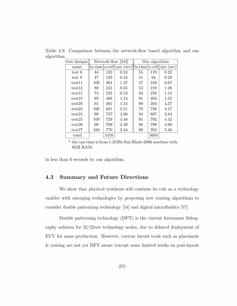
Table 4.9: Comparison between the network-flow based algorithm and ouralgorithm.
test designs Network-flow [243] Our algorithmname la.time u.cell cpu (sec)a la.time u.cell cpu (sec)
test 6 44 132 0.24 55 119 0.22test 8 47 129 0.16 41 94 0.29test11 100 264 1.37 47 249 0.67test12 80 242 0.35 52 219 1.28test15 74 233 0.53 83 230 1.15test18 88 408 1.14 91 403 1.55test20 91 382 1.24 99 393 4,27test23 100 681 2.51 78 738 4.17test24 99 737 2.06 94 807 3.84test25 100 729 3.48 91 792 4.42test26 99 709 2.49 88 798 3.98test27 100 770 3.44 99 762 5.40
total 5416 5604
a the cpu time is from 1.2GHz Sun Blade-2000 machine with8GB RAM.
in less than 6 seconds by our algorithm.
4.3 Summary and Future Directions
We show that physical synthesis will continue its role as a technology
enabler with emerging technologies by proposing new routing algorithms to
consider double patterning technology [54] and digital microfluidics [57].
Double patterning technology (DPT) is the current forerunner lithog-
raphy solution for 32/22nm technology nodes, due to delayed deployment of
EUV for mass production. However, current layout tools such as placement
& routing are not yet DPT aware (except some limited works on post-layout
255

mask decomposition). Hence, there are urgent needs to make physical design
more DPT friendly. Therefore, we present the first DPT friendly detailed
routing algorithm which performs routing and layout decomposition in one
shot, in a correct-by-construction manner. Experimental results show that
our approach outperforms the current industrial sequential approach (routing,
and then layout decomposition) by wide margin, for both quality of results and
runtime. Also, our results imply that DPT should be considered even in earlier
design stages in order to generate a fully DPT compatible layout. Therefore,
we plan to research on DPT compatible standard cell design techniques (e.g.,
pin shape and location) and DPT aware placement algorithms.
Digital microfluidic biochip design is expected to be in larger scale with
higher complexity shortly due to its various applications and high efficiency. In
order to cope with droplet routing automation, one of the key steps in digital
microfluidic biochip design, we propose a high-performance droplet router with
timing and fault-tolerance taken into account. Experiments demonstrate that
our algorithm works significantly better than the widely used prioritized A*
search and the state-of-the-art network-flow based algorithm.
256

Chapter 5
Conclusion
This dissertation presents our effort in physical synthesis for nanometer
VLSI and emerging technologies. Our major contributions include:
• We develop physical synthesis algorithms to address key challenges in
nanometer VLSI, floorplanning for substrate noise, clock synthesis under
thermal effect, and global routing for routability, in order to improve
design closure. Especially, our BoxRouter significantly advanced the-
state-of-the-art in global routing which has been believed as a solved
problem for many years, at the time of publication with best paper
nomination in DAC’06. Therefore, BoxRouter brought up large attention
from academia and industry with over excellent 20 follow-up papers in
the past 2 years, which finally leads to successful ISPD routing contests.
(Chapter 2)
• We propose the first manufacturability aware routing framework where
three major challenges (topography variation, random defects, and print-
ability) are addressed during global, track, and detailed routing respec-
tively according to the characteristics of the issue. Most of early/previous
design-for-manufacturability (DFM) efforts are limited by post-optimization
257

strategies, but our routing framework demonstrates the potential of true
DFM, based on design-time consideration of manufacturing effects in a
correct-by-construction manner. (Chapter 3)
• We show that physical synthesis will continue its role as a technology
enabler with emerging technologies by proposing new routing algorithms
to consider double patterning technology and digital microfluidics. We
show that our 40 year expertise and infrastructure in VLSI physical
synthesis can be highly leveraged for emerging technologies, as long as
we fully understand the nature of them. Our droplet routing algorithm
for digital microfluidic biochips is a paragon. (Chapter 4)
In this dissertation, we emphasize the importance of routing in multiple
critical problems. We hope that this work will motivate excellent research
follow-ups in this domain. Some of the future directions may include:
• Most current optimizations for manufacturability are performed indepen-
dently, but different manufacturability issues are indeed highly related
with each other such as critical area, lithography, and CMP. Improving
one aspect (e.g., critical area) may make other aspects (e.g., lithography)
worse, and vice verse. Therefore, holistic modeling and optimization of
all key manufacturability effects into some “global” yield metric will be
in great demand. This should be a future direction for manufacturability
aware routing.
258
• For sub 22nm nodes, Extreme Ultra-Violet lithography (EUVL) may be
introduced to product lines, if it can be deployed successfully in time. It
is known that EUVL suffers from strong flare effect, which is also strongly
layout density/pattern dependent. Therefore, manufacturability aware
design still plays a very important role, yet we need to take different
DFM approaches to deal with EUVL or other next generation lithog-
raphy by developing different manufacturing models and corresponding
optimization techniques in physical synthesis.
• As the variations grow, we need more vertical integration through the
system-circuit-synthesis co-optimization. By understanding pros/cons of
each approach at each design level, we can find the most effective solution
at the lowest overhead across whole system-circuit-synthesis flow for a
certain challenge by harmonizing multiple approaches.
259

Bibliography
[1] S. N. Adya and I. L. Markov. Fixed-outline Floorplanning : Enabling
Hierarchical Design. IEEE Trans. on Very Large Scale Integration
(VLSI) Systems, 11:120–1135, Dec 2003.
[2] K. Ahn and S. Sahni. Constrained via minimization. IEEE Trans. on
Computer-Aided Design of Integrated Circuits and Systems, 12:273–282,
Feb 1993.
[3] A. H. Ajami, M. Pedram, and K. Banergee. Effects of non-uniform
substrate temperature on the clock signal integrity in high performance
designs. In Proc. IEEE Custom Integrated Circuits Conf., 2001.
[4] S. Akella and S. Hutchinson. Coordinating the motions of multiple
robots with specified trajectories. In Proc. Int. Conf. Robotics and
Automation, 2002.
[5] C. Albrecht. Global Routing by New Approximation Algorithms for
Multicommodity Flow. IEEE Trans. on Computer-Aided Design of
Integrated Circuits and Systems, 20(5):622–632, May 2001.
[6] F. Alizadeh and D. Goldfarb. Second-order cone programming. Math.
Programming Ser. B, 95, 2003.
260

[7] Farid Alizadeh. Interior point methods in semidefinite programming
with applications to combinatorial optimization. SIAM Journal on Op-
timization, 5, 1995.
[8] G. A. Allan. Targeted Layout Modifications for Semiconductor Yield/Reliability
Enhancement. IEEE Trans. on Semiconductor Manufacturing, 17(4):573–
581, Nov 2004.
[9] C. J. Alpert, A. Devgan, and S.T. Quay. Buffer insertion for noise and
delay optimization. In Proc. Design Automation Conf., pages 362–7,
June 1998.
[10] C. J. Alpert, T. C. Hu, J. H. Huang, and A. B. Kahng. A direct combina-
tion of the Prim and Dijkstra constructions for improved performance-
driven global routing. In Proc. IEEE Int. Symp. on Circuits and
Systems, pages 1869–1872, 1993.
[11] Erling Andersen, Cees Roos, and Tamas Terlaky. On implementing
a primal-dual interior-point method for conic quadratic optimization.
Math. Programming, 95, 2003.
[12] W. Arnold. Towards 3nm overlay and critical dimension uniformity:
an integrated error budget for double patterning lithography. In Proc.
SPIE 6924, 2008.
[13] George E. Bailey, Alexander Tritchkov, Jea-Woo Park, Le Hong, Vincent
Wiaux, Eric Hendrickx, Staf Verhaegen, Peng Xie, and Janko Versluijs.
261

Double pattern EDA solutions for 32nm HP and beyond. In Proc. SPIE
6521, 2007.
[14] H. B. Bakoglu. Circuits, Interconnections, and Packaging for VLSI.
Addison-Wesley Publishing Company, 1990.
[15] C. Bamji and E. Malavasi. Enhanced network flow algorithm for yield
optimization. In Proc. Design Automation Conf., 1996.
[16] K. Banergee, A. H. Ajami, and M. Pedram. Analysis and optimization
of thermal issues in high-performance VLSI. In Proc. Int. Symp. on
Physical Design, pages 230–237, Apr 2001.
[17] Shabbir Batterywala, Narendra Shenoy, William Nicholls, and Hai Zhou.
Track Assignment: A Desirable Intermediate Step Between Global Rout-
ing and Detailed Routing. In Proc. Int. Conf. on Computer Aided
Design, 2002.
[18] Karl F. Bohringer. Modeling and Controlling Parallel Tasks in Droplet-
based Microfluidic Systems. IEEE Trans. on Computer-Aided Design
of Integrated Circuits and Systems, 25:329–339, Feb 2006.
[19] Murat R. Becer, David Blaauw, Rajendran Panda, and Ibrahim N. Hajj.
”early probabilistic noise estimation for capacitively coupled intercon-
nects”. IEEE Trans. on Computer-Aided Design of Integrated Circuits
and Systems, pages 77–83, Mar 2003.
262
[20] C. Bencher, Y. Chen, H. Dai, W. Montgomery, and L. Hul. 22nm half-
pitch patterning by cvd spacer self alignment double patterning (sadp).
In Proc. SPIE 6924, 2008.
[21] P. Berman, A. B. Kahng, D. Vidhani, H. Wang, and A. Zelikovsky.
Optimal Phase Conflict Removal for Layout of Dark Field Alternating
Phase Shifting Masks. In Proc. Int. Symp. on Physical Design, Apr
1999.
[22] G. Blakiewicz, M. Jeske, M. Chrzanowska-Jeske, and J. S. Zhang. Sub-
strate Noise Modeling in Early Floorplanning of Mixed-Signal SOCs. In
Proc. Asia and South Pacific Design Automation Conf., pages 819–823,
Jan 2005.
[23] T. Blalack, Y. Leclercq, and C. P. Yue. On-chip RF isolation techniques.
In Proc. IEEE BCTM., pages 205–211, 2002.
[24] K. D. Boese and A. B. Kahng. Zero-skew clock routing trees with
minimum wirelength. In Proc. IEEE Int. Conf. ASIC, Sep 1992.
[25] M. Born and E. Wolf. Principles of Optics, 6th Edision. Pergamon
Press, 1980.
[26] M. Born and E. Wolf. Principles of Optics : Electromagnetic The-
ory of Propagation, Interference and Diffraction of Light, 7th Edition.
Cambridge University Press, 1999.
263
[27] Y. Bourai and C.-J. Richard Shi. Layout compaction for yield optimiza-
tion via critical area minimization. In Proc. Design, Automation and
Test in Eurpoe, 2000.
[28] S. Boyd and L. Vandenberghe. Convex Optimization. Cambridge, 2004.
[29] Ulrich Brenner and Andre Rohe. An Effective Congestion-Driven Place-
ment Framework. IEEE Trans. on Computer-Aided Design of Inte-
grated Circuits and Systems, 22(4):387–394, Apr 2003.
[30] M. Burstein and R. Pelavin. Hierarchical Wire Routing. IEEE Trans.
on Computer-Aided Design of Integrated Circuits and Systems, 2(4):223–
234, Oct 1983.
[31] Zhen Cao, Tom Tong Jing, Jinjun Xiong, Yu Hu, Zhe Feng, Lei He,
and Xian-Long Hong. Fashion: A fast and accurate solution to global
routing problem. IEEE Trans. on Computer-Aided Design of Integrated
Circuits and Systems, 27(4):726–737, Apr 2008.
[32] Zhen Cao, Tong Jing, Jinjun Xiong, Yu Hu, Lei He, and Xianlong Hong.
DpRouter: A Fast and Accurate Dynamic-Pattern-Based Global Rout-
ing Algorithm. In Proc. Asia and South Pacific Design Automation
Conf., 2007.
[33] Gregory Chaitin. Register allocation and spilling via graph coloring.
SIGPLAN Not., 39(4):66–74, 2004.
264

[34] A. Chakraborty, K. Duraisami, A. Sathanur, P. Sithambaram, L. Benini,
A. Macii, E. Macii, and M. Poncino. Dynamic thermal clock skew
compensation using tunable delay buffers. In Proc. Int. Symp. on Low
Power Electronics and Design, 2006.
[35] A. Chakraborty, P. Sithambaram, K. Duraisami, A. Macii, E. Macii, and
M. Poncino. Thermal resilient bounded-skew clock tree optimization
methodology. In Proc. Design, Automation and Test in Eurpoe, 2006.
[36] H. H. Chan, S. N Adya, and I. L. Markov. Are Floorplan Representa-
tions Important In Digital Design? In Proc. Int. Symp. on Physical
Design, Apr 2005.
[37] Chin-Chih Chang and J. Cong. An efficient approach to multilayer layer
assignment with an application to via minimization. IEEE Trans. on
Computer-Aided Design of Integrated Circuits and Systems, 18(5):608–
620, May 1999.
[38] K. C. Chang and H. C. Du. Layer assignment problem for three-layer
routing. IEEE Trans. on Computers, 37(5):625–632, May 1988.
[39] Y.-C. Chang, Y.-W. Chang, G.-M. Wu, and S.-W. Wu. B*-Ttrees:
A New Representation for Non-Slicing Floorplans. In Proc. Design
Automation Conf., Jun 2000.
[40] G. J. Chatin. Register Allocation & Spilling via Graph Coloring. In
Proc. Symp. on Compiler Construction, 1982.
265

[41] F. Chen, J. Gill, and D. Harmon. Measurements of effective thermal
conductivity for advanced interconnect structure with various composite
low-k dielectrics. In Proc. Int. Reliability Physics Symp., 2004.
[42] Hongyu Chen, Changge Qiao, Feng Zhou, and Chung-Kuan Cheng. Re-
fined Single Trunk Tree: A Rectilinear Steiner Tree Generator For In-
terconnect Prediction. In Proc. System-Level Interconnect Prediction,
Apr 2002.
[43] T.-C. Chen and Y.-W. Chang. Modern Floorplanning Based on Fast
Simulated Annealing. In Proc. Int. Symp. on Physical Design, Apr
2005.
[44] Tai-Chen Chen and Yao-Wen Chang. Routability-driven and Opti-
cal Proximity Correction-aware Multilevel Full-Chip Gridless Routing.
IEEE Trans. on Computer-Aided Design of Integrated Circuits and Sys-
tems, 26, 2007.
[45] Tai-Chen Chen, Guang-Wan Liao, and Yao-Wen Chang. Predictive
Formulae for OPC with Applications to Lithography-friendly Routing.
In Proc. Design Automation Conf., Jun 2008.
[46] Tung-Chieh Chen, Minsik Cho, David Z. Pan, and Yao-Wen Chang.
Metal-Density Driven Placement for CMP Variation and Routability.
In Proc. Int. Symp. on Physical Design, Apr 2008.
266
[47] Yongseok Cheon, Pei-Hsin Ho, Andrew B. Kahng, Sherief Reda, and
Qinke Wang. Power-aware placement. In Proc. Design Automation
Conf., pages 795–800, New York, NY, USA, 2005. ACM Press.
[48] T.-Y. Chiang, B. Shieh, and K.C. Sarawat. Impact of Joule heating on
scaling of deep sub-micron Cu/low-k interconnects. In Proc. Symp. on
VLSI Technology, Digest of Technical Papers, pages 38–39, Jun 2002.
[49] V. K. R. Chiluvuri and I. Koren. Layout-Synthesis Techniques for
Yield Enhancement. IEEE Trans. on Semiconductor Manufacturing,
8(2):178–187, May 1995.
[50] M. Cho, S. Ahmed, and David Z. Pan. TACO: Temperature aware clock
optimization. In Proc. Int. Conf. on Computer Aided Design, 2005.
[51] M. Cho and D. Z. Pan. BoxRouter: A new global router based on box
expansion and progressive ILP. In Proc. Design Automation Conf., Jul
2006.
[52] M. Cho, H. Shin, and D. Z. Pan. Fast substrate noise-aware floorplan-
ning with preference directed graph for mixed-signal SOCs. In Proc.
Asia and South Pacific Design Automation Conf., Jan 2006.
[53] M. Cho, H. Xiang, R. Puri, and D. Z. Pan. Wire Density Driven Global
Routing for CMP Variation and Timing. In Proc. Int. Conf. on
Computer Aided Design, Nov 2006.
267

[54] Minsik Cho, Yongchan Ban, and David Z. Pan. Double Patterning Tech-
nology Friendly Detailed Routing. In Proc. Int. Conf. on Computer
Aided Design, Nov 2008.
[55] Minsik Cho and David Z. Pan. BoxRouter: a new global router based on
box expansion and progressive ilp. In Proc. Design Automation Conf.,
pages 373–378, San Francisco, CA, Jul 2006.
[56] Minsik Cho and David Z. Pan. BoxRouter: A New Global Router Based
on Box Expansion and Progressive ILP. IEEE Trans. on Computer-
Aided Design of Integrated Circuits and Systems, (12):2130–2143, Dec
2007.
[57] Minsik Cho and David Z. Pan. A High Performance Droplet Router for
Digital Microfluidic Biochips. In Proc. Int. Symp. on Physical Design,
Apr 2008.
[58] Minsik Cho, Hua Xiang, Ruchir Puri, and David Z. Pan. Wire Density
Driven Global Routing for CMP Variation and Timing. In Proc. Int.
Conf. on Computer Aided Design, Nov 2006.
[59] Minsik Cho, Hua Xiang, Ruchir Puri, and David Z. Pan. TROY: Track
Router with Yield-driven Wire Planning. In Proc. Design Automation
Conf., Jun 2007.
[60] Minsik Cho, Kun Yuan, Yongchan Ban, and David Z. Pan. ELIAD:
Efficient Lithography Aware Detailed Router with Compact Post-OPC
268

Printability Prediction. In Proc. Design Automation Conf., Jun 2008.
[61] S. K. Cho, S. K. Fan, H. Moon, and C. J. Kim. Toward digital microflu-
idic circuits: Creating, transporting, cutting and merging liquid droplets
by electrowetting-based actuation. In Proc. Micro Electro Mechanical
Systems (MEMS) Conf., Jan 2002.
[62] Sung Kwon Cho, Hyejin Moon, and Chang-Jin Kim. Creating, Trans-
porting, Cutting, and Merging Liquid Droplets by Electrowetting-Based
Actuation for Digital Microfluidic Circuits. Journal of Microelectrome-
chanical Systems, 12(1):70 – 80, Feb 2003.
[63] Chris C. N. Chu. FLUTE: Fast Lookup Table Based Wirelength Es-
timation Technique. In Proc. Int. Conf. on Computer Aided Design,
2004.
[64] N. B. Cobb. Fast Optical and Process Proximity Correction Algorithms
for Integrated Circuit Manufacturing. PhD thesis, University of Califor-
nia at Berkeley, 1998.
[65] J. Cong, A. B. Kahng, C.-K. Koh, and C.-W. A. Tsao. Bounded-
skew clock and Steiner routing. ACM Trans. on Design Automation of
Electronics Systems, 3(3):341–338, Jul 1998.
[66] Jason Cong. Advanced Routing Techniques for Nanometer IC Designs.
In Proc. Int. Conf. on Computer Aided Design, Nov 2006.
269

[67] J. P. Costa, M. Chou, and L. M. Silveria. Efficient Techniques for Ac-
curate Modeling and Simulation of Substrate Coupling in Mixed-Signal
IC’s. IEEE Trans. on Computer-Aided Design of Integrated Circuits
and Systems, 18(5):597–607, May 1999.
[68] Phillip Cristie and Jose Pineda de Gyvez. Prelayout Interconnect Yield
Prediction. IEEE Trans. on Very Large Scale Integration (VLSI) Sys-
tems, 11(1):55–59, Feb 2003.
[69] David Cross, Eric Nequist, and Louis Scheffer. A DFM Aware, Space
Based Router. In Proc. Int. Symp. on Physical Design, Mar 2007.
[70] Jose Pineda de Gyvez. Yield modeling and beol fundamentals. In Proc.
System-Level Interconnect Prediction, 2001.
[71] L. Deferm, C. Claes, and G. J. Declerck. Two- and Three-Dimensional
Calculation of Substrate Resistance. IEEE Trans. on Electron Devices,
35(3):339–352, Mar 1988.
[72] Jiyang Dong, Junying Zhang, and Zhong Chen. Neural Network Based
Algorithm for Multi-Constrained Shortest Path Problem. Springer Berlin
/ Heidelberg, 2007.
[73] Martin Drapeau, Vincent Wiaux, Eric Hendrickx, Staf Verhaegen, and
Takahiro Machida. Double Patterning Design Split Implementation and
Validation for the 32nm Node. In Proc. SPIE 6521, 2007.
270

[74] G. Cornuejols E. Balas, S. Ceria and N. Natraj. Gomory Cuts Revisited.
In Operations Research Letters, volume 19, 1996.
[75] S. J. Fang, T. H. Smith, G. B. Shinn, J. A. Stefani, and D. S. Boning.
Advanced Process Control in Dielectric Chemical Mechanical Polishing
(CMP). In Chemical Mechanical Polish for ULSI Multilevel Intercon-
nection Conf., Feb 1999.
[76] R. Feynman. There’s plenty of room at the bottom: An invitation to
enter a new field of physics. In Engrg Sci., 1960.
[77] D. Z. Pan G. Xu, R. Tian and M. D. F. Wong. CMP Aware Shuttle Mask
Floorplanning. In Proc. Asia and South Pacific Design Automation
Conf., Jan 2005.
[78] B. S. Gallardo, V. K. Gupta, F. D. Eagerton, L. I. Jong, V. S. Craig,
R. R. Shah, and N. L. Abbott. Electrochemical principles for active
control of liquids on submillimeter scales. Science, 283:57–60, Jan 1999.
[79] Jhih-Rong Gao, Pei-Ci Wu, and Ting-Chi Wang. High-performance
Routing at the Nanometer Scale. In Proc. Asia and South Pacific
Design Automation Conf., Jan 2008.
[80] M.R. Garey and D.S. Johnson. Computers and Intractability: A Guide
to the Theory of NP-Completeness. W.H. Freeman, 1979.
271

[81] T. E. Gbondo-Tugbawa. Chip-Scale Modeling of Pattern Dependencies
in Copper Chemical Mechanical Polishing Process. PhD thesis, Mas-
sachusetts Institute of Technology, 2002.
[82] Ranjit Gharpurey and Robert G. Meyer. Modeling and Analysis of
Substrate Coupling in Integrated Circuits. IEEE J. Solid-State Circuits,
31(3):344–353, Mar 1996.
[83] Reinhard Glang. Defect Size Distribution In VLSI Chips. IEEE Trans.
on Semiconductor Manufacturing, 4(4):265–269, Nov 1991.
[84] E. J. Griffith, S. Akella, and M. K. Goldberg. Performance characteriza-
tion of a reconfigurable planar array digital microfluidic system. IEEE
Trans. on Computer-Aided Design of Integrated Circuits and Systems,
25(2):340–352, Feb 2006.
[85] P. Gronowski et al. High performance microprocessor design. IEEE J.
Solid-State Circuits, 33:676–686, May 1998.
[86] P. N. Guo, C. K. Cheng, and T. Yoshimura. An O-Tree Representa-
tion of Non-Slicing Floorplan and Its Applications. In Proc. Design
Automation Conf., 1999.
[87] P. Gupta, A. B. Kahng, and C.-H. Park. Detailed Placement for Im-
proved Depth of Focus and CD Control. In Proc. Asia and South Pacific
Design Automation Conf., Jan 2005.
272

[88] U. I. Gupta, D. T. Lee, and J. Y.-T. Leung. An Optiaml Solution for
the Channel-Assignment Problem. IEEE Trans. on Computer-Aided
Design of Integrated Circuits and Systems, c-28(11):807–810, Nov 1979.
[89] R. T. Hadsell and P. H. Madden. Improved Global Routing through
Congestion Estimation. In Proc. Design Automation Conf., Jun 2003.
[90] Hali Han. Synthesized Compact Models for Substrate Noise Coupling
in Mixed-Signal ICS. In Ph.D. Thesis, Stanford University, 2006.
[91] L. He, A. B. Kahng, K. Tam, and J. Xiong. Design of Integrated-Circuit
Interconnects with Accurate Modeling of CMP. In Proc. SPIE 5756,
Mar 2005.
[92] M. V. Heijingen, M. Badarouglu, S. Donnay, G. G. E Gielen, and H. J. D.
Man. Substrate Noise Generation in Complex Digital Systems: Efficient
Modeling and Simulation Methodology and Experimental Verification.
IEEE J. Solid-State Circuits, 37(8):1065–1072, Aug 2002.
[93] K. Helsgaun. An Effective Implementation of the Lin-Kernighan Trav-
eling Salesman Heuristic. European Journal of Operational Research,
126(1), 2000.
[94] T.-Y. Ho, Y.-W. Change, S.-J. Chen, and D. T. Lee. A Fast Crosstalk-
and Performance-Driven Multilevel Routing System. In Proc. Int.
Conf. on Computer Aided Design, Nov 2003.
[95] http://vlsicad.eecs.umich.edu/BK/parquet.
273

[96] http://vlsicad.ucsd.edu/GSRC/bookshelf/Slots/BST/.
[97] http://www.akira.ruc.dk/∼keld/research/LKH.
[98] http://www.cse.ucsc.edu/research/surf/GSRC/MCNC.
[99] http://www.cs.mcgill.ca/∼aghnei/mmain.html.
[100] http://www.diku.dk/geosteiner/.
[101] http://www.ece.ucsb.edu/∼kastner/labyrinth/.
[102] http://www.gnu.org/software/glpk/glpk.html/.
[103] http://www.ispd.cc/ispd07 contest.html.
[104] http://www.mosek.com.
[105] http://www.praesagus.com/.
[106] J. Hu and S. Sapatnekar. A Timing-Constrained Algorithm for Simul-
taneous Global Routing of Multimple Nets. In Proc. Int. Conf. on
Computer Aided Design, 2000.
[107] J. Hu and S. Sapatnekar. A Survey On Multi-net Global Routing for
Integrated Circuits. Integration, the VLSI Journal, 31(1):1–49, Nov
2002.
[108] Jin Hu, Jarrod A. Roy, and Igor L. Markov. Sidewinder: a scalable
ilp-based router. In Proc. System-Level Interconnect Prediction, 2008.
274

[109] Shiyan Hu and Jiang Hu. Pattern sensitive placement for manufactura-
bility. In Proc. Int. Symp. on Physical Design, Mar 2007.
[110] L. Huang and D. F. Wong. Optical Proximity Correction (OPC)-
Friendly Maze Routing. In Proc. Design Automation Conf., Jun 2004.
[111] Judy Huckabay, Wolf Staud, Robert Naber, Anton van Oosten, Peter
Nikolski, Stephen Hsu, R. J. Socha, M. V. Dusa, and Donis Flagello.
Process results using automatic pitch decomposition and double pat-
terning technology (DPT) at k1eff < 0.20. In Proc. SPIE 6349, 2006.
[112] E. P. Huijbregtz, H. Xue, and Jochen A.G. Jess. Routing for Reli-
able Manufacturing. IEEE Trans. on Semiconductor Manufacturing,
8(2):188–194, May 1995.
[113] K. Ichimura, S. Oh, and M. Nakagawa. Light-driven motion of liquids
on a photoresponsive surface. Science, 288:1624–1626, Jun 2000.
[114] T. Iizuka, M. Ikeda, and K. Asada. Exact Wiring Fault Minimization
via Comprehensive Layout Synthesis for CMOS Logic Cells. In Proc.
Int. Symp. on Quality Electronic Design, Mar 2004.
[115] S. Im and K. Banerjee. Full chip thermal analysis of planar (2-d) and
vertically integrated (3-d) high performance ICs. In Tech. Dig. IEEE
International Electron Devices Meeting, Dec 2000.
275

[116] S. Im, N. Srivastava, K. Banerjee, and K. E. Goodson. Scaling Analy-
sis of Multilevel Interconnect Temperatrues for High-Performance ICs.
IEEE Trans. on Electron Devices, 52(12):2710–2719, Dec 2005.
[117] Y. Inazuki, N. Toyama, T. Nagai, T. Sutou, Y. Morikawa, H. Mohri,
N. Hayashi, M. Drapeau, K. Lucas, and C. Cork. Decomposition diffi-
culty analysis for double patterning and the impact on photomask man-
ufacturability. In Proc. SPIE 6925, 2008.
[118] T. B. Jones, M. Gunji, M. Washizu, and M. J. Feldman. Dielec-
trophoretic liquid actuation and nanodroplet formation. Journal of
Applied Physics, 89:1441–1448, Jan 2001.
[119] A. B. Kahng. Key Directions and a Roadmap for Electrical Design for
Manufacturability. In Proc. European Solid-State Circuits Conf, 2007.
[120] A. B. Kahng, B. Liu, and I. I. Mandoiu. Non-tree routing for reliability
and yield improvement. In Proc. Int. Conf. on Computer Aided Design,
Nov 2002.
[121] A. B. Kahng, C.-H. Park, and X. Xu. Fast Dual-Graph Based Hot-
Spot Detection. In Proc. BACUS Symp. on Photomask Technology and
Management, 2006.
[122] Andrew B. Kahng, Shailesh Vaya, and Alexander Zelikovsk. New Graph
Bipartizations for Double-Exposure, Bright Field Alternating Phase-
276

Shift Mask Layout. In Proc. Asia and South Pacific Design Automation
Conf., Jan 2001.
[123] J. Kao, A. Chandrakasan, and D. Antoniadis. Transistor sizing issues
and tool for multi-threshold CMOS technology. In Proc. Design Au-
tomation Conf., 1997.
[124] W. H. Kao and W. K. Chu. Noise constraint driven placement for
mixed signal designs. In Proc. IEEE Int. Symp. on Circuits and
Systems, pages 712–715, 2003.
[125] R. Kastner, E. Bozorgzadeh, and Majid Sarrafzadeh. Pattern Routing:
Use and Theory for Increasing Predictability and Avoiding Coupling.
IEEE Trans. on Computer-Aided Design of Integrated Circuits and Sys-
tems, 21(7):777–790, Jul 2002.
[126] Rony Kay and Rob A. Rutenbar. Wire packing: A strong formulation of
crosstalk-aware chip-level track/layer assignment with an efficient integer
programming solution. In Proc. Int. Symp. on Physical Design, 2000.
[127] D. A. Kirkpatrick and A. L. Sangiovanni-Vincentelli. Techniques For
Crosstalk Avoidance In The Physical Design Of High-performance Dig-
ital Systems. In Proc. Int. Conf. on Computer Aided Design, 1994.
[128] Wen H. Ko. Trends and frontiers of MEMS . Sensors and Actuators A:
Physicals, 136:62–67, May 2007.
277

[129] Tim Kong, Hardy Leung, Vivek Raghavan, Alfred K. Wong, and Sarah
Xu. Model-assisted routing for improved lithography robustness. In
Proc. SPIE 6521, 2007.
[130] I. Koren. Should Yield be a Design Objective? In Proc. Int. Symp. on
Quality Electronic Design, Mar 2000.
[131] A. Koukab, K. Banerjee, and M. Declercq. Modeling Techniques and
Verification Methdologies for Substrate Coupling Effects in Mixed-signal
System-on-Chip designs. IEEE Trans. on Computer-Aided Design of
Integrated Circuits and Systems, 23(6):823– 836, Jun 2004.
[132] Y. Ku. Lithography challenges and solution for 32nm node and beyond.
In Proc. Asia and South Pacific Design Automation Conf., Jan 2008.
[133] S.-Y. Kuo. YOR: a yield-optimizing routing algorithm by minimizing
critical areas and vias. IEEE Trans. on Computer-Aided Design of
Integrated Circuits and Systems, 12(9):1303–1311, Sep 1993.
[134] T. Kutzschebauch and L. Stok. Congestion aware layout driven logic
synthesis. In Proc. Int. Conf. on Computer Aided Design, Nov 2001.
[135] S. Lakshminarayanan, P. J. Wright, and J. Pallinti. Electrical char-
acterization of the copper CMP process and derivation of metal layout
rules. IEEE Trans. on Semiconductor Manufacturing, 16(4):668–676,
Nov 2003.
278

[136] Hai Lan, Zhiping Yu, and Robert W. Dutton. A cad-oriented modeling
approach of frequency-dependent behavior of substrate noise coupling
for mixed-signal ic design. In Proc. Int. Symp. on Quality Electronic
Design, pages 195–200, Mar 2003.
[137] Kuang-Yao Lee and Ting-Chi Wang. Post-routing redundant via inser-
tion for yield/reliability improvement. In Proc. Asia and South Pacific
Design Automation Conf., 2006.
[138] Sang-Soo Lee and D. J. Allstot. Electrothermal simulation of integrated
circuits. IEEE J. Solid-State Circuits, 28(12):1283–1293, Dec 1993.
[139] Won-Seok Lee, Keun-Ho Lee, Jin-Kyu Park, Tae-Kyung Kim, and Young-
Kwan Park. Investigation of the capacitance deviation due to metal-fills
and the effective interconnect geometry modeling. In Proc. Int. Symp.
on Quality Electronic Design, Nov 2003.
[140] Hardy Kwok-Shing Leung. Advanced routing in changing technology
landscape. In Proc. Int. Symp. on Physical Design, 2003.
[141] L. W. Liebmann. Layout impact of resolution enhancement techniques:
impediment or opportunity? In Proc. Int. Symp. on Physical Design,
2003.
[142] C. Lin and D.M.W. Leenaerts. A New Efficient Method Substrate-
Aware Device-Level Placement. In Proc. Asia and South Pacific Design
Automation Conf., pages 533–536, 2000.
279

[143] I-Jye Lin, Tsui-Yee Ling, and Yao-Wen Chang. Statistical Circuit Op-
timization Considering Device and Interconnect Process Variations. In
Proc. System-Level Interconnect Prediction, March 2007.
[144] J.-M. Lin and Y.-W. Chang. TCG-S:Orthogonal Coupling of P*-admissible
Representations for General Floorplans. In Proc. Design Automation
Conf., pages 842–847, 2002.
[145] M. S. Lobo, L. Vandenverghe, S. Boyd, and H. Lebret. Applications of
second-order cone programming. Linear Algebra and its Applications,
248, 1998.
[146] C. Long and L. He. Distributed sleep transistor network for power
reduction. In Proc. Design Automation Conf., 2003.
[147] J. Lou, S. Krishnamoorthy, and H. S. Sheng. Estimating Routing Con-
gestion using Probabilistic Analysis. In Proc. Int. Symp. on Physical
Design, 2001.
[148] K. Lucas, C. Cork, A. Miloslavsky, G. Luk-Pat, L. Barnes, J. Hapli,
J. Lewellen, G. Rollins, V. Wiaux, and S. Verhaegen. Interactions
of double patterning technology with wafer processing, opc and design
flows. In Proc. SPIE 6924, 2008.
[149] W. Maly. Modeling of Lithography Related Yield Losses for CAD of
VLSI Circuits. IEEE Trans. on Computer-Aided Design of Integrated
Circuits and Systems, 4(3):166–177, Jul 1985.
280

[150] W. Maly, H. Heineken, J. Khare, and P. K. Nag. Design for Manufac-
turability in Submicron Domain. In Proc. Int. Conf. on Computer
Aided Design, Nov 1996.
[151] M. Mani, A. Devgan, and M. Orshansky. An Efficient Algorithm for
statistical Minimization of Total Power under Timing Yield Constraints.
In Proc. Design Automation Conf., Jun 2005.
[152] C. Mead and L. Conway. Introduction to VLSI Systems. Addison-
Wesley, 1980.
[153] Ruchir Puri Minsik Cho, Hua Xiang and David Z. Pan. TROY: Track
Routing and Optimization for Yield. IEEE Trans. on Computer-Aided
Design of Integrated Circuits and Systems, 27(5):872–882, May 2008.
[154] J. Mitra, P. Yu, and D. Z. Pan. RADAR: RET-Aware Detailed Rout-
ing Using Fast Lithography Simulations. In Proc. Design Automation
Conf., Jun 2005.
[155] S. Mitra, R. A. Rutenbar, L. R. Carley, and D. J. Allstot. Susbtrate-
Aware Mixed-Signal Macrocell Placement in WRIGHT. IEEE J. Solid-
State Circuits, 30(3):269–278, Mar 1995.
[156] Hans D. Mittelmann. An Independent Benchmarking of SDP and SOCP
Solvers. Math. Programming Ser. B, 95, 2003.
[157] Michael D. Moffitt. Maizerouter: engineering an effective global router.
In Proc. Asia and South Pacific Design Automation Conf., Jan 2008.
281
[158] Mosin Mondal, Andrew Ricketts, Sami Kirolos, Tamer Ragheb, Greg
Link, Vijaykrishnan Narayanan, and Yehia Massoud. Mitigating ther-
mal effects on clock skew with dynamically adaptive drivers. In Proc.
Int. Symp. on Quality Electronic Design, 2007.
[159] Mosin Mondal, Andrew J. Ricketts, Sami Kirolos, Tamer Ragheb, Greg
Link, N. Vijaykrishnan, and Yehia Massoud. Thermally robust clocking
schemes for 3d integrated circuits. In Proc. Design, Automation and
Test in Eurpoe, 2007.
[160] Tamal Mukherjee. Design Automation Issues for Biofluidic Microchips.
In Proc. Int. Conf. on Computer Aided Design, Nov 2005.
[161] Dirk Muller. Optimizing yield in global routing. In Proc. Int. Conf.
on Computer Aided Design, 2006.
[162] H. Murata, K. Fujiyoshi, S. Nakatake, and Y. Kajitani. VLSI Module
Placement Based on Rectangle-Packing by the Sequence-Pair. IEEE
Trans. on Computer-Aided Design of Integrated Circuits and Systems,
15(12):1518–1524, Dec 1996.
[163] N.J. Naclerio, S. Masuda, and K. Nakajima. The via minimization
problem is NP-complete. IEEE Trans. on Computers, 38(11):1604–
1608, Nov 1989.
[164] A. Nardi, H. Zeng, J. L. Garrett, L. Daniel, and A. L. S-Vincentelli. A
Methodology for the computation of an upper bound on noise current
282

spectrum of CMOS swichting activity. In Proc. Int. Conf. on Computer
Aided Design, pages 778–785, 2003.
[165] Alessandra Nardi and Alberto L. Sangiovanni-Vincentelli. Logic Syn-
thesis for Manufacturability. In IEEE Design & Test of Computers,
May 2004.
[166] Y. Nesterov and A. Nemirovskii. Interior Point Polynomial Algorithms
in Convex Programming. SIAM Publications, Philadelphia, Pennsylva-
nia, USA, 1994.
[167] Y. E. Nesterov and M. Todd. Self-scaled barriers and interior-point
methods for convex programming. Mathematics of Operations Research,
22, 1997.
[168] J. Oh and M. Pedram. Gated clock routing for low-power microprocessor
design. IEEE Trans. on Computer-Aided Design of Integrated Circuits
and Systems, 20(6):715–722, Jun 2001.
[169] A. Osyczka. Multicriterion Optimization in Engineering - with FOR-
TRAN Programs. Ellis Horwood, 1984.
[170] B.E. Owens, S. Adluri, P. Birrer, R. Shreeve, S. K. Arunachalam, and
K. Mayaram. Simulation and Measurement of Supply and Substrate
Noise in Mixed-Signal ICs. IEEE J. Solid-State Circuits, 40(2):382–
391, Feb 2005.
283

[171] Muhammet Mustafa Ozdal and Martin D. F. Wong. ARCHER: A
HISTORY-DRIVEN GLOBAL ROUTING ALGORITHM. In Proc. Int.
Conf. on Computer Aided Design, Nov 2007.
[172] D. Ozis, T. Fiez, and K. Mayaram. An Efficient Modeling Approach
for Substrate Noise Coupling Analysis. In Proc. IEEE Int. Symp. on
Circuits and Systems, 2002.
[173] D. Ozis, T. Fiez, and K. Mayaram. Comprehensive geometry-dependent
macromodel for substrate noise coupling in heavily doped cmos pro-
cesses. In Proc. IEEE Custom Integrated Circuits Conf., 2002.
[174] David Z. Pan and Minsik Cho. Synergistic physical synthesis for man-
ufacturability/variability in 45nm designs and beyond. In Proc. Asia
and South Pacific Design Automation Conf., Jan 2008.
[175] Min Pan and Chris Chu. FastRoute: A Step to Integrate Global Routing
into Placement. In Proc. Int. Conf. on Computer Aided Design, 2006.
[176] Min Pan and Chris Chu. Fastroute 2.0: A high-quality and efficient
global router. In Proc. Asia and South Pacific Design Automation
Conf., 2007.
[177] Evanthia Papadopoulou and D. T. Lee. Critical Area Computation
via Voronoi Diagrams. IEEE Trans. on Computer-Aided Design of
Integrated Circuits and Systems, 18(4):463–474, Apr 1999.
284

[178] Jungchul Park, Stephen Hsu, Douglas Van Den Broeke, J. Fung Chen,
Mircea Dusa, Robert Socha, Jo Finders, Bert Vleeming, Anton van
Oosten, Peter Nikolsky, Vincent Wiaux, Eric Hendrickx, Joost Bekaert,
and Geert Vandenberghe. Application Challenges with Double Pattern-
ing Technology (DPT) beyond 45nm. In Proc. SPIE 6349, 2006.
[179] Y.C. Pati, A.A. Ghazanfarian, and R.F. Pease. Exploiting Structure in
Fast Aerial Image Computation for Integrated Circuit Patterns. IEEE
Trans. on Semiconductor Manufacturing, 10(1):62–74, Feb 1997.
[180] J. Peng and S. Akella. Coordinating multiple robots with kinodynamic
constraints along specified paths. In Proc. Workshop Algorithmic Foun-
dations Robotics, 2002.
[181] A. Pitaksanonku, S. Thanawastien, C. Lursinsap, and J.A. Gandhi. Dtr:
A defect-tolerant routing algorithm. In Proc. Design Automation Conf.,
1989.
[182] M. G. Pollack, A. D. Shenderov, and R. B. Fair. Electrowetting-based
actuation of droplets for integrated microfluidics. In Lab on a Chip,
volume 2, pages 96 – 101, 2002.
[183] R. Puri, L. Stok, J. Cohn, D. Kung, D. Pan, D. Sylvester, A. Srivastava,
and S. H. Kulkarni. Pushing ASIC Performance in a Power Envelope.
In Proc. Design Automation Conf., 2003.
285

[184] Xiaoning Qi, Alex Gyure, Yansheng Luo, Sam C. Lo, Mahmoud Shahram,
and Kishore Singhal. Emerging technologies: Measurement and charac-
terization of pattern dependent process variations of interconnect resis-
tance, capacitance and inductance in nanometer technologies. In ACM
Great Lakes Symp. on VLSI, Apr 2006.
[185] H. Ren, D. Z. Pan, C. Alpert, G.-J. Nam, and P. Villarrubia. Hip-
pocrates: First-Do-No-Harm detailed placement. In Proc. Asia and
South Pacific Design Automation Conf., pages 141–146, Jan 2007.
[186] H. Ren, D. Z. Pan, C. Alpert, and P. Villarrubia. Diffusion Based
Placement Migration. In Proc. Design Automation Conf., Jun 2005.
[187] H. Ren, D. Z. Pan, and D. S. Kung. Sensitivity guided net weighting for
placement driven synthesis. In Proc. Int. Symp. on Physical Design,
2004.
[188] H. Ren, D. Z. Pan, and P. Villarrubia. True crosstalk aware incremental
placement with noise map. In Proc. Int. Conf. on Computer Aided
Design, pages 616–619, 2004.
[189] H. Ren, D.Z. Pan, and P. Villarrubia. True Crosstalk Aware Incremental
Placement with Noise Map. In Proc. Int. Conf. on Computer Aided
Design, Nov 2004.
[190] Jarrod A. Roy and Igor L. Markov. High-performance Routing at the
Nanometer Scale. In Proc. Int. Conf. on Computer Aided Design, Nov
286
2007.
[191] J. Rubinstein and A. Neureuther. Post-decomposition assessment of
double patterning layouts. In Proc. SPIE 6924, 2008.
[192] T. S. Sammarco and M. A. Burns. Thermocapillary pumping of discrete
droplets in microfabricated analysis devices. AIChe Journal, 45:350–
366, 1999.
[193] P. Saxena and S. Gupta. On Integrating Power and Signal Routing
for Shield Count Minimization in Congested Regions. IEEE Trans. on
Computer-Aided Design of Integrated Circuits and Systems, 22(4):437–
445, Apr 2003.
[194] Semiconductor Industry Association. International Technology Roadmap
for Semiconductors, 2007, http://public.itrs.net/.
[195] Apo Sezginer and Bayram Yenikaya. Double Patterning Technology:
Process-Window Analysis in a Many-Dimensional Space. In Proc. SPIE
6521, 2007.
[196] R. Singh. A Review of Substrate Coupling Issues and Modeling Strate-
gies. In Proc. IEEE Custom Integrated Circuits Conf., pages 491–499,
1999.
[197] V. Srinivasan, V.K. Pamula, and R.B. Fair. An Integrated Digital Mi-
crofluidic Lab-on-a-chip for Clinical Diagnostics on Human Physiological
Fluids. In Lab on a Chip, volume 4, pages 310 – 315, Aug 2004.
287

[198] A. Srivastava, D. Sylvester, and D. Blaauw. Concurrent Sizing, Vdd and
Vth Assignment for Low-Power Design. In Proc. Design, Automation
and Test in Eurpoe, volume 1, pages 718–719, Feb 2004.
[199] F. Su and K. Chakrabarty. Architectural-level synthesis of digital
microfluidics-based biochips. In Proc. Int. Conf. on Computer Aided
Design, Nov 2004.
[200] F. Su and K. Chakrabarty. Module Placement for Fault-Tolerant Microfluidics-
Based Biochips. ACM Trans. on Design Automation of Electronics
Systems, 11(3):682–710, Jul 2006.
[201] Fei Su, Krishnendu Chakrabarty, and Richard B. Fair. Microfluidics-
Based Biochips: Technology Issues, Implementation Platforms, and Design-
Automation Challenges. IEEE Trans. on Computer-Aided Design of
Integrated Circuits and Systems, 25(2):211–223, Feb 2006.
[202] Fei Su, W. Hwang, and Krishnendu Chakrabarty. Droplet Routing
in the Synthesis of Digital Microfluidic Biochips. In Proc. Design,
Automation and Test in Eurpoe, 2006.
[203] J. Z. Su and W. Dai. Post route optimization for improved yield using
a rubber-band wiring model. In Proc. Int. Conf. on Computer Aided
Design, Nov 1997.
[204] X. Tang and D.F. Wong. Floorplanning with Alignment and Perfor-
mance Constraints. In Proc. Design Automation Conf., Jun 2002.
288
[205] R. Tian, D. F. Wong, and R. Boone. Model-Based Dummy Feature
Placement for Oxide Chemical-Mechanical Polishing Manufacturability.
IEEE Trans. on Computer-Aided Design of Integrated Circuits and Sys-
tems, 20(7):902–910, Jul 2001.
[206] Ivor Wai-Hung Tsang and James Tin-Yau Kwok. Efficient Hyperkernel
Learning Using Second-Order Cone Programming. IEEE Trans. on
Neural Networks, 17(1):48–58, Jan 2006.
[207] R-S. Tsay. An Exact Zero Skew Clock Routing Algorithm. IEEE
Trans. on Computer-Aided Design of Integrated Circuits and Systems,
12(2):242–249, Feb 1993.
[208] Hsiao-Ping Tseng, Louise Scheffer, and Carl Sechen. Timing- and
Crosstalk-Driven Area Routing. IEEE Trans. on Computer-Aided De-
sign of Integrated Circuits and Systems, 20(4):528–544, April 2001.
[209] A. Vanleenhove and D. Steenwinckel. A litho-only approach to double
patterning. In Proc. SPIE 6521, 2007.
[210] N. K. Verghese and J. J. Allstot. Computer-aided design considerations
in Mixed-signal coupling in RF integration circuits. IEEE J. Solid-State
Circuits, 33(3):314–323, Mar 1998.
[211] Nishath K. Verghese and David J. Allstot. Rapid Simulation of Sub-
strate Coupling Effects in Mixed-Mode ICs. In Proc. IEEE Custom
Integrated Circuits Conf., pages 18.3.1– 18.3.4, 1993.
289

[212] Nishath K. Verghese, David J. Allstot, and Mark A. Wolfe. Fast Par-
asitic Extraction for Substrate Coupling in Mixed-Signal ICs. In Proc.
IEEE Custom Integrated Circuits Conf., pages 7.2.1–7.2.4, 1996.
[213] P. M. B. Vitanyi. How Well Can a Graph Be n-Colored? Discrete
Math., 34:69–80, 1981.
[214] A. Vittal and M. Marek-Sadowska. Crosstalk reduction for VLSI. IEEE
Trans. on Computer-Aided Design of Integrated Circuits and Systems,
16(3):290–298, Mar 1997.
[215] D.M.H Walkter. Yield Simulation for Integrated Circuits. Kluwer
Academic Publishers, 1987.
[216] T. Wang and C.C. Chen. Power-Delivery Networks Optimization with
Thermal Reliability Integrity. In Proc. Int. Symp. on Physical Design,
April 2004.
[217] T. Y. Wang and C. P. Chen. 3-D Thermal-ADI: A Linear-Time Chip
Level Transient Thermal Simulator. IEEE Trans. on Computer-Aided
Design of Integrated Circuits and Systems, 21(12):1434–1445, Dec 2002.
[218] D.M. Warme. Spanning Trees in Hypergraphs with Applications to
Steiner Trees. PhD thesis, Computer Science Dept., The University
of Virginiay, 1998.
[219] Hou Wenting, Yu Hong, Hong Xianlong, Cai Yiciand Wu Weimin, Gu Jun
Gu, and W.H. Kao. A new congestion-driven placement algorithm based
290

on cell inflation. In Proc. Asia and South Pacific Design Automation
Conf., Jan 2001.
[220] J. Westra, C. Bartels, and P. Groeneveld. Probabilistic Congestion
Prediction. In Proc. Int. Symp. on Physical Design, Apr 2004.
[221] J. Westra, C. Bartels, and P. Groeneveld. Is Probabilistic Congestion
Estimation Worthwhile? In Proc. System-Level Interconnect Prediction,
Apr 2005.
[222] J. Westra, P. Groeneveld, T. Yan, and P. H. Madden. Global Routing:
Metrics, Benchmarks, and Tools. In IEEE DATC Electronic Design
Process, Apr 2005.
[223] V. Wiaux, S. Verhaegen, S. Cheng, F. Iwamoto, P. Jaenen, M. Maen-
houdt, T. Matsuda, S. Postnikov, and G. Vandenberghe. Split and
design guidelines for double patterning. In Proc. SPIE 6924, 2008.
[224] P. Wilkerson, A. Raman, and M. Turowski. Fast, automated thermal
simulation of three-dimensional integrated circuits. In Inter Society
Conference on Thermal Phenomena, volume 1, pages 706–713, Jun 2004.
[225] Laurence A. Wolsey. Integer Programming. J. Wiley, 1998.
[226] Stephen J. Wright. Primal-Dual Interior-Point Methods. SIAM Publi-
cations, Philadelphia, Pennsylvania, USA, 1997.
291

[227] D. Wu, J. Hu, and R. Mahapatra. Coupling Aware Timing Optimization
and Antenna Avoidance in Layer Assignment. In Proc. Int. Symp. on
Physical Design, Apr 2005.
[228] D. Wu, J. Hu, and R. Mahapatra. Antenna avoidance in layer assign-
ment. IEEE Trans. on Computer-Aided Design of Integrated Circuits
and Systems, 25(4):734–74, Apr 2006.
[229] D. Wu, J. Hu, M. Zhao, and R. Mahapatra. Timing Driven Track
Routing Considering Coupling Capacitance. In Proc. Asia and South
Pacific Design Automation Conf., 2005.
[230] Di Wu, Jiang Hu, Rabi Mahapatra, and Min Zhao. Layer assignment
for crosstalk risk minimization. In Proc. Asia and South Pacific Design
Automation Conf., Jan 2004.
[231] Q. Wu, Q. Qiu, and M. Pedram. Dynamic power management of com-
plex systems using generalized stochastic Petri nets. In Proc. Design
Automation Conf., Jun 2000.
[232] Yun-Ru Wu, Ming-Chao Tsai, and Ting-Chi Wang. Maze Routing
with OPC Consideration. In Proc. Asia and South Pacific Design
Automation Conf., Jan 2005.
[233] H. Xiang, X. Tang, and M. D. F. Wong. Bus-Driven Floorplanning.
IEEE Trans. on Computer-Aided Design of Integrated Circuits and Sys-
tems, 23(11):1522–1530, Nov 2004.
292

[234] J Xu, X. Hong, T. Jing, Y. Cai, and J. Gu. A Novel Timing-Driven
Global Routing Algorithm Considering Coupling Effects for High Per-
formance Circuit Design. In Proc. Asia and South Pacific Design Au-
tomation Conf., Jan 2003.
[235] Jingyu Xu, Subarna Sinha, and Charles C. Chiang. Accurate Detection
for Process-Hotspots with Vias and Incomplete Specification. In Proc.
Int. Conf. on Computer Aided Design, Nov 2007.
[236] Tao Xu and Krishnendu Chakrabarty. Integrated Droplet Routing in
the Synthesis of Microfluidic Biochips. In Proc. Design Automation
Conf., Jun 2007.
[237] Xiaojian Yangand, R. Kastner, and M. Sarrafzadeh. Congestion Reduc-
tion During Placement Based on Integer Programming. In Proc. Int.
Conf. on Computer Aided Design, Nov 2001.
[238] H. Yao, S. Sinha, C. Chiang, X. Hong, and Y. Cai. Efficient Process-
Hotspot Detection Using Range Pattern Matching. In Proc. Int. Conf.
on Computer Aided Design, Nov 2006.
[239] T. Yoshimura and E.S. Kuh. Efficient Algorithms for Channel Rout-
ing. IEEE Trans. on Computer-Aided Design of Integrated Circuits and
Systems, 1(1):25– 35, Jan 1982.
[240] Hao Yu, Yu Hu, Chunchen Liu, and Lei He. Minimal skew clock em-
bedding considering time variant temperature gradient. In Proc. Int.
293

Symp. on Physical Design, Apr 2007.
[241] Peng Yu, Sean X. Shi, and David Z. Pan. Process variation aware opc
with variational lithography modeling. In Proc. Design Automation
Conf., Jul 2006.
[242] P.-H. Yuh, C.-L. Yang, and Y.-W. Chang. Placement of Digital Mi-
crofluidic Biochips using the T-tree Formulation. In Proc. Design Au-
tomation Conf., Jul 2006.
[243] Ping-Hung Yuh, Chia-Lin Yang, and Yao-Wen Chang. BioRoute: A
Network Flow Based Routing Algorithm for Digital Microfluidic Biochips.
In Proc. Int. Conf. on Computer Aided Design, 2007.
[244] P. Zarkesh-Ha, S. Lakshminarayann, Ken Doniger, William Loh, and
Peter Wright. Impact of Interconnect Pattern Density Information on a
90nm Technology ASIC Design Flow. In Proc. Int. Symp. on Quality
Electronic Design, Nov 2003.
[245] S. Zhao, K. Roy, and C. Koh. Power Supply Noise Aware Floorplanning
and Decoupling Capacitace Placement. In Proc. Int. Conf. on VLSI
Design, 2003.
[246] H. Zhou and D. F. Wong. Global routing with crosstalk constraints.
IEEE Trans. on Computer-Aided Design of Integrated Circuits and Sys-
tems, 18(11):1683–1688, Nov 1998.
294

[247] Hai Zhou and D.F. Wong. Crosstalk-Constrained Maze Routing Based
on Lagrangian Relaxation. In Proc. IEEE Int. Conf. on Computer
Design, Nov 1997.
295

Index
Abstract, viii
Acknowledgments, v
Bibliography, 295
Conclusion, 257
Dedication, iv
Design Closure, 6
Emerging Technologies, 197
Introduction, 1
Manufacturing Closure, 110
296

Vita
Minsik Cho was born in Seoul, Republic of Korea on December 9th
1976, the son of Wonkyu Cho and Jongsook Hong. He received the Bachelor
of Science degree in Electrical Engineering from the Seoul National University
in 1999. After 3 year military service, he moved to United State in August
2002 and received the Master of Science degree in Electrical and Computer
Engineering from University of Wisconsin Madison in 2004. He was accepted
to Electrical and Computer Engineering Department in University of Texas at
Austin and started graduate studies with Prof. David Z. Pan in August, 2004.
He decides to join IBM T. J. Watson Research Center in August, 2008 after
his Ph.D. degree in Electrical and Computer Engineering.
His main research includes various physical synthesis algorithms with
emphasis on routing for efficient design and manufacturing closures. During
the Ph.D. program, he worked for Intel (Austin, TX) during Summer 2005 and
for IBM Research (Yorktown, NY) during Summer 2006, where he researched
on power modeling and manufacturability aware router respectively. He was
invited back to IBM Research (Yorktown, NY) again for Summer 2007 to work
on pioneering paralell physical synthesis and timing closure.
The impacts of his research were recognized with Best Paper Nomi-
nations in ASPDAC’06 and DAC’06, ACM/SIGDA Awards in 2007 (ISPD’07
297

Routing Contest), IEEE/CEDA Award in 2007 (BoxRouter open source), IBM
Ph.D. Scholarship in 2007, and SRC Inventor Recognition Award in 2008.
Book/Book Chapter
B1. Minsik Cho, Joydeep Mitra, and David Z. Pan, “Manufacturability AwareRouting,” in The Handbook of Algorithms for VLSI Physical Design Automa-tion, CRC Press (Invited) (edited by Dr. Charles J. Alpert, Prof. Dinesh P.Mehta, and Prof. Sachin S. Sapatnekar)
Journal Articles
J8. Minsik Cho, Kun Yuan, Yongchan Ban and David Z. Pan, “ELIAD: Effi-cient Lithography Aware Detailed Router with Macro Compact Post-OPCPrintability Prediction,” submitted to IEEE Transaction on Computer-AidedDesign of Integrated Circuits and Systems (TCAD)
J7. Tung-Chieh Chen, Minsik Cho, David Z. Pan, and Yao-Wen Chang, “Metal-Density Driven Placement for CMP Variation and Routability,” under minorrevision for IEEE Transaction on Computer-Aided Design of Integrated Cir-cuits and Systems (TCAD)
J6. Minsik Cho and David Z. Pan, “A High-Performance Droplet Routing Al-gorithm for Digital Microfluidic Biochips,” accepted to IEEE Transaction onComputer-Aided Design of Integrated Circuits and Systems (TCAD)
J5. Minsik Cho, Katrina Lu, Kun Yuan, and David Z. Pan, “BoxRouter 2.0: AHybrid and Robust Global Router with Layer Assignment for Routability,”under minor revision for ACM Transactions on Design Automation of Elec-tronic Systems (TODAES)
J4. David Z. Pan, Peng Yu, Minsik Cho, Anand Ramalingam, Kiwoon Kim,Anand Rajaram, and Sean X. Shi, “Nanometer IC Design and Process Inte-gration: A Survey,” The Journal of Process Control (JPC), Jun 2008
J3. Minsik Cho and David Z. Pan, “Fast Substrate Noise-Aware Floorplanningwith Preference Directed Graph for Mixed-Signal SOCs,” accepted to IEEETransaction on Very Large Scale Integration Systems (TVLSI)
298

J2. Minsik Cho, Hua Xiang, Ruchir Puri, and David Z. Pan, “TROY: TrackRouting and Optimization for Yield,” IEEE Transaction on Computer-AidedDesign of Integrated Circuits and Systems (TCAD), Vol. 27, No. 5, May2008
J1. Minsik Cho and David Z. Pan, “BoxRouter: A New Global Router Based onBox Expansion and Progressive ILP,” IEEE Transaction on Computer-AidedDesign of Integrated Circuits and Systems (TCAD), Vol. 26, No. 12, Dec2007
Conference Papers
C13. Minsik Cho, Yongchan Ban, and David Z. Pan, “Double Patterning Technol-ogy Friendly Detailed Routing,” Proc. IEEE/ACM International Conferenceon Computer-Aided Design (ICCAD), Nov 2008
C12. Minsik Cho, Kun Yuan, Yongchan Ban and David Z. Pan, “ELIAD: EfficientLithography Aware Detailed Router with Compact Post-OPC PrintabilityPrediction,” Proc. SRC Techcon, Sep 2008
C11. Minsik Cho, Kun Yuan, Yongchan Ban and David Z. Pan, “ELIAD: EfficientLithography Aware Detailed Router with Compact Post-OPC PrintabilityPrediction,” Proc. ACM/IEEE Design Automation Conference (DAC), Jun2008
C10. Tung-Chieh Chen, Minsik Cho, David Z. Pan, and Yao-Wen Chang, “Metal-Density Driven Placement for CMP Variation and Routability,” Proc. ACMInternational Symposium on Physical Design (ISPD), Apr 2008
C9. Minsik Cho and David Z. Pan, “A High Performance Droplet Router for Dig-ital Microfluidic Biochips,” Proc. ACM International Symposium on PhysicalDesign (ISPD), Apr 2008
C8. David Z. Pan and Minsik Cho, “Synergistic Physical Synthesis for Manufac-turability and Variability in 45nm Designs and Beyond,” Proc. ACM/IEEEAsian and South Pacific Design Automation Conference (ASPDAC), Jan 2008
C7. Minsik Cho, Katrina Lu, Kun Yuan and David Z. Pan, “BoxRouter 2.0: Ar-chitecture and Implementation of a Hybrid and Robust Global Router,” Proc.IEEE/ACM International Conference on Computer-Aided Design (ICCAD),Nov 2007
299
C6. Minsik Cho, Hua Xiang, Ruchir Puri and David Z. Pan, “TROY: TrackRouter with Yield-driven Wire Planning,” Proc. ACM/IEEE Design Au-tomation Conference (DAC), Jun 2007
C5. Minsik Cho, Hua Xiang, Ruchir Puri and David Z. Pan, “Wire Density DrivenGlobal Routing for CMP Variation and Timing,” Proc. IEEE/ACM Interna-tional Conference on Computer-Aided Design (ICCAD), Nov 2006
C4. Minsik Cho and David Z. Pan, “BoxRouter: A New Global Router Based onBox Expansion and Progressive ILP,” Proc. ACM/IEEE Design AutomationConference (DAC), Jul 2006
C3. Minsik Cho and David Z. Pan, “PEAKASO: Peak-Temperature Aware Scan-vector Optimization,” IEEE VLSI Test Symposium (VTS), Apr 2006
C2. Minsik Cho, Hongjoong Shin, and David Z. Pan, “Fast Substrate Noise-Aware Floorplanning with Preference Directed Graph for Mixed-Signal SOCs,”Proc. ACM/IEEE Asian and South Pacific Design Automation Conference(ASPDAC), Jan 2006
C1. Minsik Cho, Suhail Ahmed, and David Z. Pan, “TACO: Temperature AwareClock Optimization,” Proc. IEEE/ACM International Conference on Computer-Aided Design (ICCAD), Nov 2005
Permanent address: 114-1002 Moraksan Hyundai APT, Ohjen-dong,Kyunggi-do, Republic of Korea
This dissertation was typeset with LATEX† by the author.
†LATEX is a document preparation system developed by Leslie Lamport as a specialversion of Donald Knuth’s TEX Program.
300