Embed Size (px)
Citation preview

Comparison of 32nm High-k Metal Gate Predictive Technology Model CMOS and MOSFET-Like CNFET compact Model Based Domino logic Circuits
Saravana Maruthamuthu, Wireless Group
Infineon Technologies India Private Limited,
MOS-AK/GSA Workshop, December 8th 2010, San Francisco (CA)

Set date Page 2Copyright © Infineon Technologies 2010. All rights reserved.
Outline
Domino logic 32nm Predictive Technology Model (PTM) basedAND, OR gate cells are compared with MOSFET-like CarbonNano-FET (CNFET) model based AND, OR gate cells
The analysis done at 25oC and 110oC in HSPICE.
Static Power, Dynamic Power and Delay measurements aredone

Predictive Technology Model (PTM) Low Power 32nm Metal Gate / High-K / Strained-Si
NMOS Characteristics ofBSIM 4.0 Level 54 NominalPredictive Technology ModelGenerated using the onlinetool of Arizona StateUniversity
Leff 12.6nm
Vth 0.16V
Vdd 0.9V
Tox 1nm
Rdsw 150 Ohm
Set date Copyright © Infineon Technologies 2010. All rights reserved. Page 3

Stanford Single Walled-CNFET MOSFET-like HSPICE Compact Model Characteristics
Set date Copyright © Infineon Technologies 2010. All rights reserved. Page 4
Schematic and model parameters of
CNFET compact model
CNFET drain current vs. drain-to-source voltage (VDS)
with 0.9V VGS and
substrate (back gate) grounded
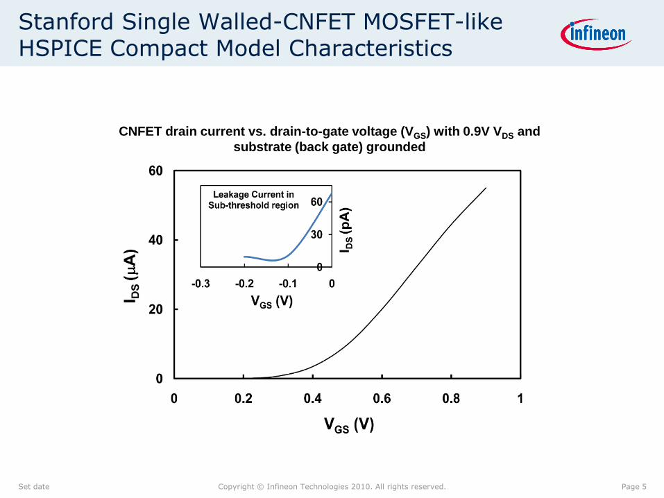
Stanford Single Walled-CNFET MOSFET-like HSPICE Compact Model Characteristics
Set date Copyright © Infineon Technologies 2010. All rights reserved. Page 5
CNFET drain current vs. drain-to-gate voltage (VGS) with 0.9V VDS and
substrate (back gate) grounded

Domino Gates: AND, OR
Set date Copyright © Infineon Technologies 2010. All rights reserved. Page 6
Domino AND Gate Domino OR Gate
VDD = 0.9V for both CNFET and 32nm CMOS
Load Capacitance = 0.0002pF

32nm CMOS and CNFET Transistor Dimensions
Transistor Channel
Width (w)
x 10-9 m
M1 80
M2 32
M3 80
M4 40
M5 40
M6 40
M7 40
Set date Copyright © Infineon Technologies 2010. All rights reserved. Page 7
32nm CMOS PTM Dimensions
for Domino AND, OR Gates
Channel Length = 32nm
VDD = 0.9V
CNFET Gate Width
(Wg)
x 10-9 m
Chirality
Vector of
CNT (m,n)
CNT
Count
M1 40 (16,0) 1
M2 32 (16,0) 1
M3 40 (16,0) 1
M4 50 (19,0) 2
M5 50 (19,0) 2
M6 50 (19,0) 2
M7 50 (19,0) 2
CNFET Dimensions for Domino AND, OR Gates
Gate Length (Lg) = 20nm
VDD = 0.9V

Simulation Results
Domino Gate
Type
Static Power
at 25oC
in Pico watt
Static power
at 110oC
in Pico watt
32nm PTM
CMOS AND 9065 17962
CNFET AND 80.47 348
32nm PTM
CMOS OR
9214 18516
CNFET OR 92.70 578.60
Set date Copyright © Infineon Technologies 2010. All rights reserved. Page 8
Static Power Measurement through DC Analysis

Simulation Results
Set date Copyright © Infineon Technologies 2010. All rights reserved. Page 9
Dynamic Power of Domino AND Gate During Transient Analysis
Temp = 25oC Temp = 110oC
x 1
0-7
watt

Simulation Results
Set date Copyright © Infineon Technologies 2010. All rights reserved. Page 10
Delay Measurement using Transient Analysis for Domino AND Gate
Temp = 25oC Temp = 110oC
De
lay i
n P
ico
Se
co
nd

Simulation Results
Set date Copyright © Infineon Technologies 2010. All rights reserved. Page 11
Dynamic Power of Domino OR Gate During Transient Analysis
Temp = 25oC Temp = 110oC
x 1
0-7
watt

Simulation Results
Set date Copyright © Infineon Technologies 2010. All rights reserved. Page 12
Delay Measurement using Transient Analysis for Domino OR Gate
Temp = 25oC Temp = 110oC
De
lay i
n P
ico
Se
co
nd

Conclusion
On comparison at 25oC and 110oC, the CNFET domino OR gateconsumes nearly 100% less static power than CMOS DominoOR gate.
Transient power of CNFET domino OR is nearly 43% lesser thanits CMOS counterpart.
Delay of CNFET Domino OR is 40% lesser than that of CMOSgate.
In case of Domino AND, CNFET AND gate offers reduction instatic power by 99% and transient power of CNFET DominoAND is nearly 40% lesser than that of 32nm CMOS DominoAND gate.
In terms of delay, CNFET AND gate is 36% faster than CMOSgate. The overall static and dynamic power consumption of thegate is higher at 110oC.
Set date Copyright © Infineon Technologies 2010. All rights reserved. Page 13
References
[1] Neil H.E Weste, David Harris, Ayan Banerjee, “CMOS VLSI DESIGN” Third edition, Pearson Education 2006.
[2] M. Saravana, "Ultra Low Power Dual-Gate 6T and 8T Stack Forced CNFET SRAM Cells”, MOS-AK workshop Rome, April 2010. http://www.mos-ak.org/rome/posters.php
[3] Stanford University CNFET HSPICE Model website http://nano.stanford.edu/model.php?id=23.
[4] PTM High Performance 16nm Metal Gate / High-K /Model, Nanoscale Integration and Modeling (NIMO) Group, Arizona State University, http://www.eas.asu.edu/~ptm/
[5] Jie Deng “Device Modeling and Circuit Performance Evaluation For Nanoscale Devices: Silicon Technology Beyond 45 nm Node and Carbon Nanotube Field Effect Transistors”, Stanford University, pp. 2-89, Jun. 2007.
Set date Copyright © Infineon Technologies 2010. All rights reserved. Page 14

Discussion
Set date Copyright © Infineon Technologies 2010. All rights reserved. Page 15