Embed Size (px)
Citation preview

Present Status and Future Direction of BSIM SOI ModelPresent Status and Future Direction of BSIM SOI Model
for High Performance/Low-Power/RF Applicationfor High Performance/Low-Power/RF Application
Samuel K. H. Fung, *Pin Su, *Wan Hui, *Chenming HuSamuel K. H. Fung, *Pin Su, *Wan Hui, *Chenming Hu
IBM Microelectronics, Semiconductor Research and Development Center (SRDC)
(Industrial Advisor, EECS, University of California at Berkeley)
*EECS, University of California at Berkeley, California

Agenda
•• Race between Technology and Compact ModelRace between Technology and Compact Model
•• SOI Application SpaceSOI Application Space
•• SOI Model ClassificationSOI Model Classification
•• Status of PD-SOI ModelStatus of PD-SOI Model
•• Status of FD/DD-SOI ModelStatus of FD/DD-SOI Model
•• ConclusionConclusion

Agenda
Race betweenRace between
Technology & Compact ModelTechnology & Compact Model

SOI Thickness Scaling Trend
20
30
40
5060708090
100
200
1st 0.10µm
2nd 0.13µm
0.18µm
1st 0.13µm
IBM Historic Trend
S
OI T
hick
ness
• Minimize junction capacitancewhile channel doping isincreasing with scaling
• Improve short channel control

SOI Thickness Uniformity
-6
-4
-2
0
2
4
6
-100-50
050
100
-100
-50
0
50
100-60
-40
-20
0
20
40
60
X (mm)
Mean=630.5A, std.dev.= 3A
Y (mm)
Tsi
- m
ean
(A)

Oxide Thickness and Leakage Scaling Trend
9
10
11
12
13
14
15
16
17
18
EO
T (A
)
Technology Generation1E-8
1E-7
1E-6
1E-5
Gat
e Le
akag
e @
Vdd
(A/u
m2)
• Do we understand enough on gate tunneling current?• Are compact model/characterization good enough?

Compact Model Dilemma
•• Compact Model Development requires QualifiedCompact Model Development requires QualifiedTechnology for Ultimate Verification of NewTechnology for Ultimate Verification of NewPhysicsPhysics
•• Technology with New Device Structure need GoodTechnology with New Device Structure need GoodCompact Model for Early Circuit DesignCompact Model for Early Circuit Design

Compact Model Dilemma
•• Standardized Compact Model is usually developedStandardized Compact Model is usually developedby universities.by universities.
•• It is not easy for universities to access most advancedIt is not easy for universities to access most advancedtechnology from semiconductor companiestechnology from semiconductor companies

Technology vs Compact Model
•• 0.35um0.35um
•• 0.250.25
•• 0.180.18
•• 0.130.13
•• 0.100.10
•• 0.070.07
•• 0.050.05
Technology Release(1st Product)
BSIM BulkModel
BSIM-SOI Model
•• BSIM2BSIM2–– BasicBasic
•• BSIM3BSIM3–– Poly depletionPoly depletion–– Psuedo-2D DIBL on Threshold/Psuedo-2D DIBL on Threshold/
Rout/ Subthreshold SlopeRout/ Subthreshold Slope–– HALO dopingHALO doping–– Narrow width effectNarrow width effect–– Charge partitioningCharge partitioning–– Noise modelNoise model
•• BSIM4BSIM4–– Gate tunnelingGate tunneling–– RF (Gate intrinsicRF (Gate intrinsic
resistance/substrate networkresistance/substrate network–– Asymetric S/DAsymetric S/D–– Charge Thickness ModelCharge Thickness Model
•• BSIMPD2.2BSIMPD2.2–– Diode/BJT with TAT and LDiode/BJT with TAT and L
dependencedependence–– Igb, Self-heatingIgb, Self-heating–– High Vbs MOS I-V/C-VHigh Vbs MOS I-V/C-V–– Accurate Impact IonizationAccurate Impact Ionization–– Body Contact MOSFETBody Contact MOSFET–– Noise modelingNoise modeling
•• BSIMSOI (FD/DD/PD)BSIMSOI (FD/DD/PD)–– Barrier Lowering DiodeBarrier Lowering Diode–– EtcEtc
Catch-up
Catch-up

Agenda
SOI Application SpaceSOI Application Space

SOI Application Space (1/3)
-1.2 -1.0 -0.8 -0.6 -0.4 -0.2 0.0 0.2 0.4 0.6 0.8 1.0 1.20.0
0.2
0.4
0.6
0.8
1.0
1.2
1.4
0.0
0.2
0.4
0.6
0.8
1.0
1.2
1.4
Vg=1.2, 1.0, 0.8, 0.6, 0.4, 0.2V
NFET ALgate=33nm
Ioff@1V=430nA/µm
PFETLgate=33nm
Ioff@1V=200nA/µm
Dra
in C
urre
nt (m
A/µ
m)
Drain Voltage (V)
uuWork-horse forWork-horse for
High-PerformanceHigh-Performance
MicroprocessorMicroprocessor
uuHigh Ion/Good SCEHigh Ion/Good SCE
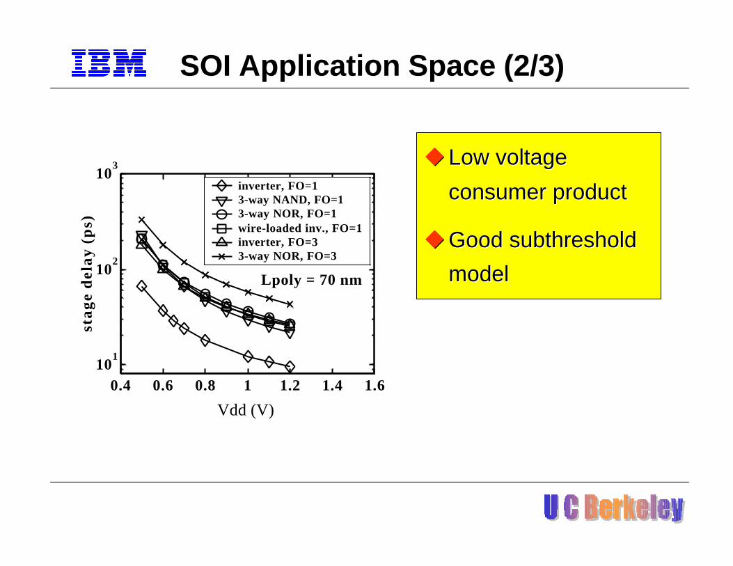
SOI Application Space (2/3)
uu Low voltageLow voltage
consumer productconsumer product
uuGood subthresholdGood subthreshold
modelmodel
0.4 0.6 0.8 1 1.2 1.4 1.610
1
102
103
stag
e d
elay
(p
s)
Lpoly = 70 nm
inverter, FO=1 3-way NAND, FO=1 3-way NOR, FO=1 wire-loaded inv., FO=1inverter, FO=3 3-way NOR, FO=3
Vdd (V)

SOI Application Space (3/3)
uMixed Signal RF
customer product
u Instrinsic gate
resistance, noise
model, layout
dependence
Id (mA/um)

SOI Application Space
•• Work-horse for High Performance micro-processorWork-horse for High Performance micro-processor
•• Emerging for low-voltage/low-power applicationEmerging for low-voltage/low-power application
•• CMOS RF applicationCMOS RF application

Agenda
SOI Model ClassificationSOI Model Classification

Classification of SOI ModelModel class Partially Depleted
(PD) BSIMPD2.2Ideal Fully
Depleted (FD)Dynamic Depletion
(DD)Progress Industrial quality, widely
adopted in industry,Standardized by CMC
on Dec 9th, 2001
Work in progress Work in progress
Devices characteristics Never get into fulldepletion
At least fullydepleted at Vg=0V
At least fully depleted atVg=Vdd
Number of nodes G, D, S, B4
G, D, S, E4
G, D, S, B, E5
Diode leakage& Gate-to-body tunnelingcurrent
Very critical Not needed Less criticalHard to formulate and
calibrateDiode capacitance& Body-to-Gate/Channelcapacitance
Very critical Not needed Less criticalHard to formulate and
calibrateSimulation Time Good Faster SlowerConvergency Demonstrated Even better Not know yetCompatibility with bulkmodel (BSIM3/BSIM4)
Essential Not necessary Essential

Agenda
Status of PD-SOI ModelStatus of PD-SOI Model

Status of PD-SOI
•• BSIMPD v2.2.1 (9/1999)BSIMPD v2.2.1 (9/1999)–– Separate BSIMPD from BSIMSOI for ease of modelSeparate BSIMPD from BSIMSOI for ease of model
implementationimplementation–– Igb model addedIgb model added–– Bug fixBug fix
•• BSIMPD v2.2.2 (2/2000) ---- Standardized by CMC 12/9/2001BSIMPD v2.2.2 (2/2000) ---- Standardized by CMC 12/9/2001–– Igb temperature dependence fixIgb temperature dependence fix–– FRBODY for layout dependent distributed RC body effectFRBODY for layout dependent distributed RC body effect–– Bug fixBug fix
•• BSIMPD v2.2.3 (2/2002)BSIMPD v2.2.3 (2/2002)–– Fix in Igb residue problemFix in Igb residue problem–– Adding dtoxcv in capMod=3 for flexibilityAdding dtoxcv in capMod=3 for flexibility–– Bug fixBug fix

BSIMPD Model Formulation
Challenges : Predict the floating body effect in DC and TransientChallenges : Predict the floating body effect in DC and Transient

BSIMPD Model Formulation
•• Extending I-V equation to Vbs close to 2*PhibExtending I-V equation to Vbs close to 2*Phib–– Vth vs VbsVth vs Vbs–– Experimental FD and DD models are included using ddModExperimental FD and DD models are included using ddMod
Body to source voltage (V)-1.0 -0.8 -0.6 -0.4 -0.2 0.0 0.2 0.4 0.6 0.8
Lin
ear
Th
resh
old
Vo
ltag
e (V
)
0.0
0.1
0.2
0.3
0.4
0.5
0.6
0.7
Temperature = 23, 85, 140C
NFETLdesign = 0.15um
0.0 0.2 0.4 0.6 0.82.4m
2.6m
2.8m
3.0m
3.2m
3.4m
3.6m
3.8m
4.0m
T=140C
T=85C
ideal BC non-ideal model measurement data
Idsa
t (A
)
Vbs (V)

BSIMPD Model Formulation
•• Impact ionization current need to be very accurateImpact ionization current need to be very accurate–– In bulk, Iii model is only for reliability understanding.In bulk, Iii model is only for reliability understanding.
Gate Voltage (V)0.5 1.0 1.5
Imp
act
Ion
izat
ion
Eff
icie
ncy
(Isu
b/Id
)
1e-5
1e-4
1e-3
1e-2
Ldesign= 0.137, 0.152, 0.172, 0.191, 0.243 µm
NFET, 85C, Vds = 1.8V
Vds (V)
0.0 0.2 0.4 0.6 0.8 1.0 1.2 1.4 1.6 1.8 2.0 2.2
Dra
in C
urr
ent
(mA
/µm
)
1e-11
1e-10
1e-9
1e-8
1e-7
1e-6
1e-5
1e-4
1e-3
Ldesign = 0.14NFET, 85C
Vgs = 0, 0.25, 0.5, 0.75, 1V

BSIMPD Model Formulation
•• Igb at accumulation and inversionIgb at accumulation and inversion
-1.5 -1.0 -0.5 0.0 0.5 1.0 1.51E-12
1E-11
1E-10
1E-9
1E-8
1E-7
1E-6
Vbs
=0V
NFET Tox = 1.45nm
-0.4V 0V Vbs
=0.4V
IgbI
gg
Igg
=Igb
Gat
e cu
rren
t (A
/µm
2 )
Vgs
(V)0.3 0.4 0.5 0.6 0.7 0.8 0.9 1.0 1.1 1.2
0
5
10
15
20
25
30
35
40
H-gate BodyContact Device
Floating Device
Ids
(µA
/µm
)
Vgs (V)
PFET Ldesign=0.125µm
Vds = 0.05V

BSIMPD Model Formulation
•• Non-ideal Body Contact SupportNon-ideal Body Contact Support–– N-segment for distributed body resistance networkN-segment for distributed body resistance network–– Parasitic diode and gate capacitanceParasitic diode and gate capacitance
Bod
y-C
onta
ct
Gate
Ext
ende
d-G
ate Drain
Source
PLC
PWC
PWB
L
W
PLD
PLS
GateGate
BC
B
B
B

BSIMPD Model Formulation
•• Floating body induced Low-Floating body induced Low-frequency Noisefrequency Noise
Dra
in C
urre
nt N
oise
Sid
(A2 /H
z)
10-21
10-20
10-19
10-18
10-17
10-16
10-15
10-14
Frequency (Hz)100 101 102 103 104 105
Out
put I
mpe
danc
e (k
Ω)
1
10
Vds=1.1V, 1.2V, 1.3V, 1.4V
W/L = 20/0.5µmTox = 8.5nmTsi = 180nmVgs = 1V
fc3 fc4fc2fc1
2 0
5Vds=1.1VVds=1.2VVds=1.3VVds=1.4V
W/L = 20/0.5µmTox = 8.5nmTsi = 180nmVgs = 1V
B: noise band width=2qI B,iii
2 =2qI B ibs2
bsii
Ground
ceq req
Body
ibs2
i2ii
(a)
Front Gate
Back Gate
Source Drainjdc
becrjs
jsc bbc
bbc : body to channel depletion cap.js/jdc : body to S/D junction cap.
ceq bb=c js+cbe+c jd+creq js=r ,(b)
jsr : body to source resistanceAC

BSIMPD Model Formulation
•• SPICE implementation allow variable nodesSPICE implementation allow variable nodes
Mname <D-node> <G-node> <S-node> <E-node> [P-node] [B-node] [T-node] <model>[TNODEOUT]
FB MOSFET ----------------------------------
BC MOSFET ----------------------------------
BC MOSFET with internal B-node available -------
FB MOSFET with temp node ------- ------------------
BC MOSFET with temp node -------------------------
BC MOSFET with internal B-node & Temp node ---
M1 (D, G, S, E)
M1 (D, G, S, E, P)
M1 (D, G, S, E, P, B)
M1 (D, G, S, E, T) TNODEOUT=1
M1 (D, G, S, E, P, T) TNODEOUT=1
M1 (D, G, S, E, P, B, T) TNODEOUT=1

Agenda
Status of FD/DD-SOI ModelStatus of FD/DD-SOI Model

Status of FD/DD-SOI
•• BSIMSOI v1.3 (1998)BSIMSOI v1.3 (1998)–– Experimental, including three models (PD/FD/DD)Experimental, including three models (PD/FD/DD)
•• BSIMFD v2.0 (9/1999)BSIMFD v2.0 (9/1999)–– Experimental, Derivative of ddMod=2 from BSIM3SOI v1.3Experimental, Derivative of ddMod=2 from BSIM3SOI v1.3
•• BSIMDD v2.0 (9/1999)BSIMDD v2.0 (9/1999)–– Experimental, Derivative of ddMod=1 from BSIM3SOI v1.3Experimental, Derivative of ddMod=1 from BSIM3SOI v1.3
•• BSIMSOI v3.0 (Mid 2002)BSIMSOI v3.0 (Mid 2002)–– Another attempt to combine PD/FD/DD modelAnother attempt to combine PD/FD/DD model–– Take advantage of CMC standardized BSIMPD2.2.3 codeTake advantage of CMC standardized BSIMPD2.2.3 code–– Fully compatible with BSIMPD2.2.3 (soimod=0)Fully compatible with BSIMPD2.2.3 (soimod=0)–– Fine tuning the concept of barrier loweringFine tuning the concept of barrier lowering–– Robust implementationRobust implementation

“Degree” of Fully Depletion
Potential at SOI bottom(Vbs0)
Tsi0PD
Assuming FD
“Degree” of FD can be measured byPotential at SOI bottom @Vg=Vth, Vd=Vs=0V assuming FD

Floating vs Not Floating (DC)
Case : We need to keep B-node for DD-SOI model
Problem : How to emulate “not floating” with floating body?
Key Concept :Key Concept :Diode with Barrier LoweringDiode with Barrier Lowering
What it means :Vbs does not change during charging/discharging.

Diode with Barrier Lowering (1/2)
H
HH
HHHHHH
H
•• Injected hole will accumulateInjected hole will accumulate
at the SOI bottomat the SOI bottom
•• The accumulation isThe accumulation is
extremely thin such that Vextremely thin such that Vbs0bs0
is still controlled by Vfg/Vbgis still controlled by Vfg/Vbg
couplingcoupling
•• The diode can sink a range ofThe diode can sink a range of
hole current with littlehole current with little
potential raisepotential raise

Diode with Barrier Lowering (2/2)
Vbs (V)
0.0 0.1 0.2 0.3 0.4 0.5 0.6 0.7
I bs (
A)
1e-15
1e-14
1e-13
1e-12
1e-11
1e-10
1e-9
1e-8
1e-7
1e-6
50nm
80nm
100nm130nm
200nm
Symbol Medici simulation Calculated by B3SOI
Tox = 10nmTbox = 400nmNch = 5e16
Vbs0
Vbs0 as a measure of the
“degree” of channel depletion
wrt SOI thickness

DD Characteristic
Vgs (V)
0.0 0.5 1.0
ds
1e-13
1e-12
1e-11
1e-10
1e-9
1e-8
1e-7
1e-6
1e-5
1e-4
MeasurementSimulated by B3SOIsymbol
Technology BLeff = 0.75µm
Ves = -3, -2, -1, 0, 1, 2V
S = 66mV/dec
S = 85mV/dec
Varying backgate bias is
the most effective way to
extract barrier lowering
effect

DD Characteristics
Vds (V)
0.0 1.0 2.0 3.0
I ds (m
A)
0
2
4
6
8
10
12
Vgs = 1V
NMOSFETW/L = 20/0.26Tsi = 50nmTbox = 85nm
Symbol Measurement Model
Vbg = -3V,
2V
3V
0V,
Varying backgate bias is
the most effective way to
extract barrier lowering
effect

Zero-field Body Potential
SOI BOX
E-field
Potential
Φs
VbsVbseff
0
Vbs definition for coupled and
decoupled case are consistent if
zero-field Vbseff is used

Range of Body Potential
Iterating Vbs (V)
-0.2 0.0 0.2 0.4 0.6 0.8 1.0
Vb
seff a
nd
Vbs
_dio
(V
)
-0.2
0.0
0.2
0.4
0.6
0.8
1.0
Vbs_dio
Vbseff
Vbs0
TSI = 50nmTBOX = 100nmNCH = 2e17VBG = -3V
2φf
Vbs0t
Vbs0
(for Diode & BJT)(for MOS IV)
DecoupledCoupled
uDecoupledØNeutral body
exist
uCoupledØNo neutral body
ØVertical E-fieldnot terminated

Agenda
ConclusionConclusion

Conclusion
•• SOI is becoming mainstream for high-performance micro-processorSOI is becoming mainstream for high-performance micro-processor
application and is emerging for low-voltage/low-power/RF SOC applicationapplication and is emerging for low-voltage/low-power/RF SOC application
•• SOI compact model is catching up heavily at 100/70nm technology node.SOI compact model is catching up heavily at 100/70nm technology node.
•• SOI model can be classified as PD, FD and DD.SOI model can be classified as PD, FD and DD.
•• BSIMPD v2.2.3 is widely adopted in industry. Almost of all important physicsBSIMPD v2.2.3 is widely adopted in industry. Almost of all important physics
are covered already.are covered already.
•• FD/DD model is currently under development. Barrier lowering concept is theFD/DD model is currently under development. Barrier lowering concept is the
key to model the FD/DD behavior.key to model the FD/DD behavior.


![online / Biannual online journal · [recensione – review] Traces d’autrui et retours sur soi, sous la direction de Perle Abbrugiati, Université de Provence, Caer – Centre](https://img.dokumen.tips/doc/110x75/5e32b23733e0887899393a5c/online-biannual-online-journal-recensione-a-review-traces-daautrui-et-retours.jpg)