Embed Size (px)
Citation preview

CMOS VLSI FrequencyTranslation for
Multi-Standard WirelessCommunication Transceivers
Jacques C. Rudell
University of California, Berkeley
Qualifying ExaminationApril 8th, 1996

page 2 of 24
High Demand for Portable Transceivers
Cellular, Cordless, and PCS transceiver units all require:
Low Cost
Low Power
Portability
1994 1995 1996 1997 1998 1999
3036.2
47.659.8
80.1
99.8
Projected World-Wide Cellular Phone Sales (units in millions)(Source:Dataquest)
Variety of RF standards
Small Form Factor
Versatility

page 3 of 24
Existing Hardware Solutions are Inefficient
Current transceiver requires many discrete components
Multi-components are highly power & cost inefficient
Multi-standard capability prohibitively large

page 4 of 24
Multi-Standard CMOS Solution
Single Chip Solution Lower Power
Increased Portability
Lower Cost
Multi-Standard Sol.
CMOS Technology
FrequencyTranslation
Frequency Translation w/o Discrete Components

page 5 of 24
Research Proposal
Examine solutions to full integration
Determine the fundamental limits of
System Contrib ution
Circuit Contrib ution
CMOS mixers in a multi-standard environment
of frequency translation system
Frequency translation w/ multi-standard capability

page 6 of 24
Receiver Issues
LNA
Gain Non-Linearities
Noise
GainNoise Figure
Distortion (IP3)
Conversion Gain
Image Rejection
Sensitivity
Detection
Selectivity&
Frequency
Translation
Desired
Undesired
fFiltering

page 7 of 24
Desired Band
Image Band
ωImage ωlo1 ωDesired
Frequency Translation Basics
ωIF
LNA Output Spectrum IF Output
LNA
LO1
IFcos( ωrf t)
cos( ωlo1t)
1/2 [ cos( ωrf - ωlo1t) + cos( ωrf + ωlo1t) ]
cos( ωrf t) • cos( ωlo1t) =
Standard Image Rejection
IS54 60dBGSM 70dBDECT 70dB
ωif = ωDesired - ωlo1 = ωlo1- ωimage

page 8 of 24
Traditional Receiver Architecture
LO1
LNA IF
I Q
LO2
A/D
Conventional Super -Heterodyne Receiver
IR SAW filter: image rejection & noise reduction
in LO 1 mixer
Bandpass IF filter reduces distortion
RF filter IR filter IF filter

page 9 of 24
Existing Approaches to Integration
LNA
I
Q
LO1
LO2
LNAI Q
LO1
Homodyne
Heterodyne w/ Image-Rejection
I Q
ϕ
Σ
Image-Reject Mixer
90o phase shifter
Zero IF, no image band present
LO leakage problem
Need for IR filter eliminated
90o phase shifter requirespassive component tuning& matching
Advantage
Disad vantage
Advantage
Disad vantage
page 10 of 24
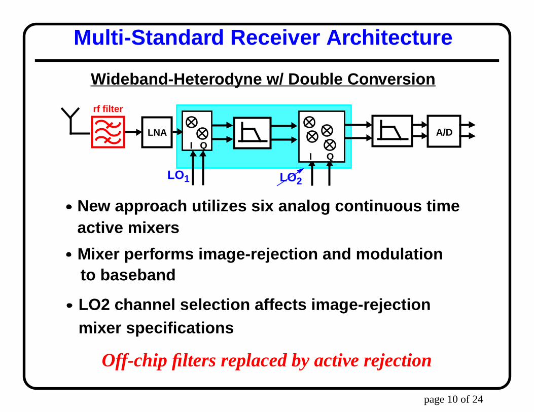
Multi-Standard Receiver Architecture
LNAI Q
I Q
LO1 LO2
A/D
New approach utilizes six analog continuous time
Wideband-Heter odyne w/ Doub le Conversion
rf filter
LO2 channel selection affects image-rejection
Mixer performs image-rejection and modulation
active mixers
to baseband
mixer specifications
Off-chip filters replaced by active rejection

page 11 of 24
I-I
I-Q
Q-I
Q-Q
LO1I
LO1Q
LO2I
LO2I
LO2Q
LO2Q
-ωLO1
2 3 4
1&3 2&4
3
2j
4&3
1,2,3&4
2&3
4&1
1&2
Q-Phase
I-Phase
j4
1
I
Q
1
ωLO1-ωIF
ωIF
-ωIF ωIF
4
1j
4&1
Image Cancellation Scheme
LNA OutputSpectrum
Desired Signal Band
Undesired Image Band
4&2
1&3

page 12 of 24
ωlo1ωrfωDesiredωimage
Image Rejection (dB)
• Pass & stop band determined by ωLO1 & ωLO2 only
• Image attenuation is independent of passive components;
New Architecture is Multi-Standard Capable
• Image-rejection mixer is programmable
exploits the odd and even properties of sine and cosine
• Sharp transition between pass & stop band
Image Rejection is self-aligning

page 13 of 24
Mixer Architectural Non-Idealities
• 30dB of IR requires I/Q phase matching better than 4 o
• 5% gain error for 30dB of image-rejection
IR (dB)
-30o
0o
30o-30o
0o30o
3060
100
Image Attentuation vs. LO phase error
60
50
40
30
200 5 10 15
IR (dB)
Image Attentuation vs. Gain Mismatch (%)
∆A(%)ϕlo2ϕlo1
• Matching is a critical issue

page 14 of 24
Mixer Topologies
Gm•Vin(t) -Gm•Vin(t)
RL RL
Vin(t)
t0 t1 t2 tN
Sampling Demodulator
Vin(t)
Passive Mix ers
Resistive/Switching
Active Mix ers
• Excellent linearity
• Low gain - conversion loss
• Poor noise performance
• Fair linearity
• Fair gain
• Clear designtrade-offs
Current Modulator
Demodulator
• No static power consumption • Static powerconsumption

page 15 of 24
Gilbert Cell Performs Current Modulation
RL RL
v rf
v lo
RERE
(Barrie Gilbert, JSSC Dec. 1968)
• Bipolar / CMOS devicesdriven w/ LO actas switches
• Input differential pair
acts as gain stage

page 16 of 24
Conversion Gain of a CMOS Gilbert Cell
g– mvrf
gmvrf
Unbalanced State
Balanced State
g– mvrf
gmvrf
vlo(t) > 2 (Vgs-Vt)
vlo(t) < 2 (Vgs-Vt)
vlo(t)
t
2tBal
gmRL
- gmRL
Conversion Gain = π2( )( )1 -
Vlo (Vgs-Vt)input
RLID2 (Vgs - Vt )sw
π2
RL RL
RL RL
Av(t)
vlo(t)
vlo(t)

page 17 of 24
Noise Performance
SSB Noise Sour ces DSB Noise Sour ces
• LO1 Mixer• Load Devices• Switches
• LO2 Mixer
• LNA• LO1 Mixer• Input Devices
• All Devices
Rin23---
Vgs Vt–( )
INI D
----------------------------------
2 2×=
RLOAD
RL2
CG2
------------ 1RL--------
I DVGS Vt–( )
LOAD------------------------------------------------+
2×=
RSW
23---
CG2--------
f lo I BVGS Vt–( )------------------------------
I B x– x x I B x–( )+[ ]
I B 2 IB x– x+( )----------------------------------------------------------------- xd
0
I B∫ 2×=
SSB Vgs Vt–( )IN
I D----------------------------------~
page 18 of 24
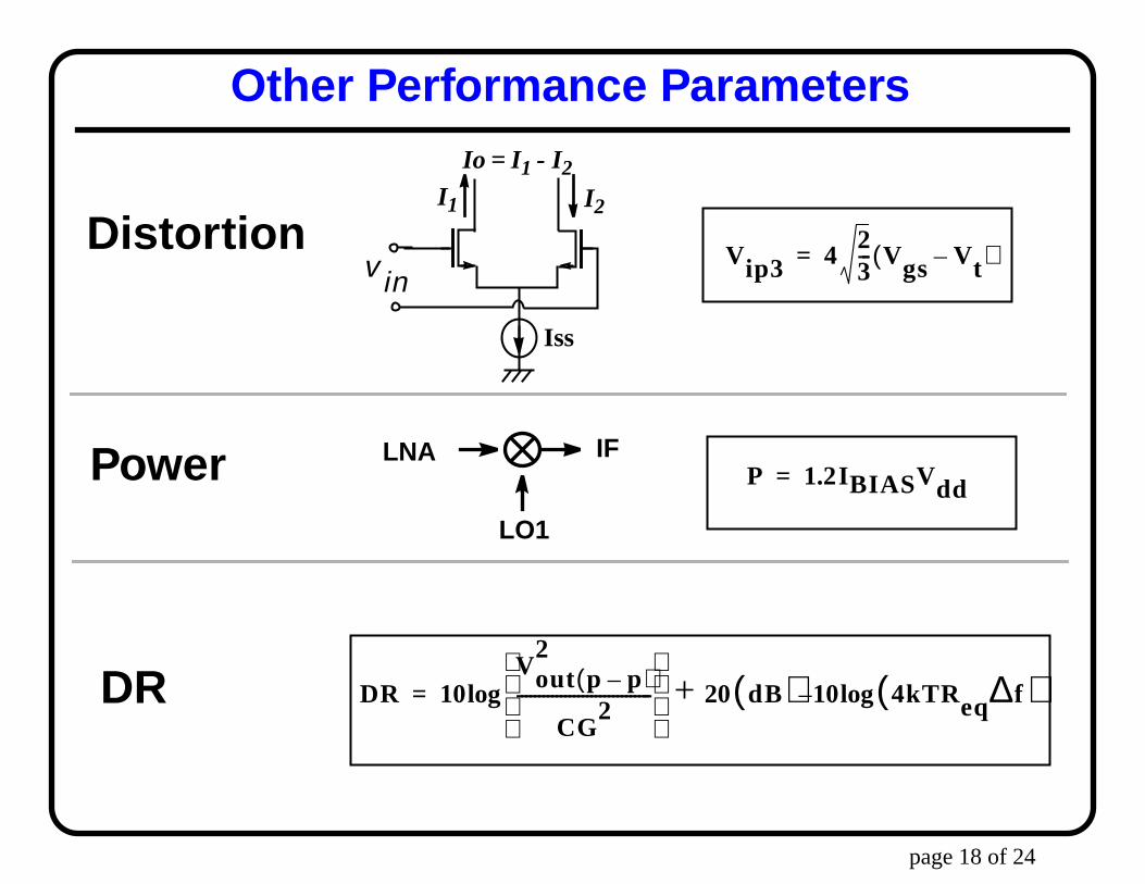
Other Performance Parameters
Vip3 423--- Vgs Vt–( )=v in
Iss
I 1 I2
Io = I 1 - I2
LNA
LO1
IFP 1.2IBIASVdd=
DR 10Vout p p–( )
2
CG2
-------------------------------
20 dB( )+log 10 4kTReq∆f( )log–=
Distortion
Power
DR

page 19 of 24
Performance Limits for Different Standards
Standard IP3 DR NFtotal NF(@LNA) Power
IS-54 25dBm 100dB 5dBGSM -5dBm 100dB 8dB 2.2dB 55mWDECT 0dBm 74dB 15dB 14dB 4.7mW802.11 +3dBm 80dB 8dB 2.2dB 55mW
Assumptions
• Gain of the LNA 20 or 0(dB)
• LO1 Mixer CG is 1
• LO2 Mixer CG is 3
Not Possible
• ReqLNA = 150Ω
• ReqBB = 82Ω

page 20 of 24
New Gilbert Cell with Variable Gain
Vrf
Vlo
Vbias1
IBias
M1 M2
M6M5M4M3
M8M7
M10
MT2MT1
M9
M13M12
M11
M14
Vocm Vout
IGain ICM
Common Mode FB
Adjustable Gain
LO Shielding
New Features

page 21 of 24
Design for the DECT Standard
LO1 Mix ers Design Issues LO2 Mix ers Design Issues
Simulated Measured
IR N/A 26dBIP3 +6dBmCG 10dB 8dBNF 2.0dB
Power 55mW 55mW
• High gain required
• Gain BW product
difficult to achieve
• LO1 & IF trade-off• DC offset due to LO
leakage
• PMOS flicker noise
• Offset compensationcurrent DAC
• AC coupling required

page 22 of 24
Comparison to Other Work
Author L(µm) IP3(dBm) NF(dB) CG(dB) RF(GHz)
D.K. Lovelace, ‘93 1.5 0 8 SSB 10.5 0.86A. Abidi, JSSC ‘96 1.0 28 4.5 DSB 0 0.9
J. Rudell & P. Gray,.. 0.6 1.8
Author, Publication RF / IF (GHz) IR(dB) NF(dB) IP3(dBm) CG(dB)
M. MacDonald, ISSCC ‘93 1.9 / 0.110 14.1 18 -12 7Steyart, JSSC Dec. ‘95 0.9 / ?? 30 24 +28 9
D.Pache, et al., CICC ‘95 2 / 0.2 35 ?? -5 10J. Rudell & P. Gray, .... 1.9 / 0.22 26
Image-Rejection Mix ers
CMOS Gilber t Cells

page 23 of 24
Expected Research Contributions
• To demonstrate the feasibility of a fully integrated
• Understand issues involved in multi-standard
• Complete behavioral understanding of the
heterodyne mixer
CMOS Gilbert cell
implementations of heterodyne mixers

page 24 of 24
Current Project Status
Project Status & Results
Prototype image-reject mixer was found fully functional w/
IP3 of the entire IR mixer is +6dBm
Entire IR mixer dissipates 55mW
Future Work.
Develop better models for noise and distortion of CMOS Gilbert cell
Compare analytical models to measured results of individual
26dB of image-rejection
Simulated results
Measured results
10dB of conversion gain
CMOS mixer testchip