Embed Size (px)
Citation preview

MCGH205-Iniewski June 5, 2011 14:13
C H A P T E R 19Digital-to-Analog
Converters for LCDs
Chih-Wen LuNational Tsing Hua University, Taiwan
The evolution of compact, lightweight, low-power, and high-quality displays has caused a large demand for liquid crystaldisplay (LCD) drivers, with features such as low power dissi-
pation, high speed, high resolution, and a large output voltage swing.An LCD driver is generally composed of column drivers, gate drivers,a timing controller, and a reference source. Column drivers are espe-cially important, and generally include registers, data latches, digital-to-analog converters (DACs), and output buffers. Among these com-ponents, the DACs and output buffers determine the column driver’sspeed, resolution, voltage swing, and power dissipation. Furthermore,DACs occupy the largest silicon area of a column driver chip. Becausea single chip includes hundreds of DACs and output buffer ampli-fiers, the DACs and buffers should occupy a small die area, and theirstatic power consumption should be small.
This chapter deals with recently reported DACs for LCD columndrivers, focusing on high-resolution and area-efficient DACs. Begin-ning with an introduction to the LCD column driver, this chapterfirst examines the commonly used resistor-string DACs (R-DACs) forLCD column driver applications. The subsequent sections describecapacitive DACs and hybrid DACs, such as resistor–capacitor DACs,embedded DACs, DACs with drain current modulation, and DACswith variable-current control interpolation.
19.1 IntroductionIn a typical column driver architecture as shown in Fig. 19.1, the col- Fig. 19.1umn driver should supply high analog voltages to the LCD panel.1−5
1

MCGH205-Iniewski June 5, 2011 14:13
2 H i g h P r e c i s i o n C i r c u i t s
FIGURE 19.1 Typicalcolumn driverarchitecture.
To reduce the power consumption, the power supply of the digitalcircuit is low voltage. Digital display data are applied to RGB inputsand sampled into input registers. A wide data latch presents one rowof serial input pixel data to the inputs of level shifters. The level shiftersthen boost the digital signals to higher levels. In the DAC of each chan-nel, a voltage level corresponding to a digital subpixel code appears atits output. The output buffers are used to drive the highly capacitivedata lines of the LCD panel.6−13
To improve the lifetime of the liquid crystal material, the liquidcrystals of active matrix liquid crystal displays (AMLCDs) should bedriven by the so-called inversion method, which alternates positive andnegative polarities between the liquid crystal cells with respect to acommon backside electrode. Designers use four inversion methodsfor AMLCD driving: frame, line, column, and dot inversions. High-quality displays prefer the dot inversion method.
Frame i
Column Drivers
+ − + −
− + − +
+ − + −
− + − +
Row
Drivers
Frame i + 1
Column Drivers
+ − + −
− + − +
+ − + −
− + − +
Row
Drivers
FIGURE 19.2Operation of thedot inversionmethod.
MCGH205-Iniewski June 5, 2011 14:13
3D i g i t a l - t o - A n a l o g C o n v e r t e r s f o r L C D s
(a)
(b)
V
V
T
T
V0
–V0
–V1023
V1023
D0 D1023
Data
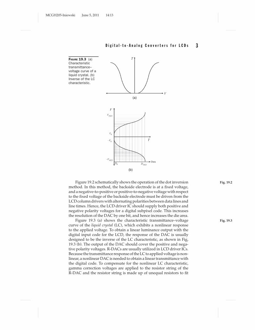
FIGURE 19.3 (a)Characteristictransmittance–voltage curve of aliquid crystal. (b)Inverse of the LCcharacteristic.
Figure 19.2 schematically shows the operation of the dot inversion Fig. 19.2method. In this method, the backside electrode is at a fixed voltage,and a negative-to-positive or positive-to-negative voltage with respectto the fixed voltage of the backside electrode must be driven from theLCD column drivers with alternating polarities between data lines andline times. Hence, the LCD driver IC should supply both positive andnegative polarity voltages for a digital subpixel code. This increasesthe resolution of the DAC by one bit, and hence increases the die area.
Figure 19.3 (a) shows the characteristic transmittance–voltage Fig. 19.3curve of the liquid crystal (LC), which exhibits a nonlinear responseto the applied voltage. To obtain a linear luminance output with thedigital input code for the LCD, the response of the DAC is usuallydesigned to be the inverse of the LC characteristic, as shown in Fig,19.3 (b). The output of the DAC should cover the positive and nega-tive polarity voltages. R-DACs are usually utilized in LCD driver ICs.Because the transmittance response of the LC to applied voltage is non-linear, a nonlinear DAC is needed to obtain a linear transmittance withthe digital code. To compensate for the nonlinear LC characteristic,gamma correction voltages are applied to the resistor string of theR-DAC and the resistor string is made up of unequal resistors to fit

MCGH205-Iniewski June 5, 2011 14:13
4 H i g h P r e c i s i o n C i r c u i t s
Digital circuits
Resister lader
Metal lines and decoders
Buffers
Metal lines and decoders
Buffers
FIGURE 19.4 Layout of a typical column driver.
the nonlinear curve. However, the area of the R-DAC and its metalrouting will be prohibitively large for a high-resolution data converter.This makes the R-DAC impractical for use in column driver integratedcircuits (ICs) for high color depth displays. As an alternative, an LCDcolumn driver using a linear switched capacitor DAC has been pro-posed. In that case, the nonlinear LC characteristic is compensated forby the timing controller, and the die area is greatly reduced.
The layout of a typical column driver is depicted in Fig. 19.4.Fig. 19.4The global resistor string, which is inserted in the center of the chip,supplies the reference voltages to all channels. Each channel needs adecoder to route the reference voltage—corresponding to the digitalinput code—to the corresponding output buffer. Since several hun-dreds of channels are built into a single chip, the die area of the rout-ing lines, used to connect the resistor string and the decoders, is verylarge. For example, 2048 metal lines are needed in a 10-bit columndriver IC. Hence, the metal lines and decoders will occupy a verylarge percentage of the column driver IC’s area, especially for highcolor depth displays.14
19.2 Resistive-String DACsIn general, R-DACs are predominantly used for LCD column drivers.The R-DAC consists of a global resistor string in the column driver ICand a decoder in each output channel, as shown in Fig. 19.5. An n-bitFig. 19.5R-DAC can be realized by using a string of 2n resistors and a 2n-to-1decoder. The global resistor string generates 2n reference voltagesand the decoder selects one of the generated reference voltages cor-responding to the digital image data to the output through the bufferamplifier. To fit the LCD panel nonlinear characteristic, some gammavoltages are applied to the resistor string and the resistor string ismade up of unequal resistors.
The R-DAC has guaranteed monotonicity and can be used forconverters up to 10-bit resolution. However, for high-resolution ap-plications, the switch components of the decoder grow exponentially

MCGH205-Iniewski June 5, 2011 14:13
5D i g i t a l - t o - A n a l o g C o n v e r t e r s f o r L C D s
From Holding Latches
VH
VL
Glo
bal R
esis
tor
Str
ing LCD
Panel−
+2n-to-1decoder
nFIGURE 19.5 R-DAC.
with the number of bits, causing a larger RC delay at the output and aprohibitively large area of switch components and the metal routinglines. This makes R-DACs impractical for use in the column driver ICfor high color depth displays.
Two types of matrix MOS switches are commonly used as thedecoder in the conventional R-DAC.15 Figure 19.6 shows a tree-type Fig. 19.6decoder DAC. The switch matrix is connected in a treelike manner, eli-minating the need for a digital decoder. For an n-bit resolution, 2n+1 – 2switch components are needed. The selected voltage propagates
FIGURE 19.6Tree-type-decoderR-DAC.

MCGH205-Iniewski June 5, 2011 14:13
6 H i g h P r e c i s i o n C i r c u i t s
FIGURE 19.7Digital-decoderR-DAC.
through n levels of switches before arriving at the buffer amplifier.For a high-resolution converter, the switch network may cause a se-rious delay. For high-speed applications, the tree-type decoder is re-placed with a digital decoder shown in Fig. 19.7. In this structure,Fig. 19.7even though the common node of all the switches is connected to thebuffer amplifier, producing a large capacitive load, the selected voltagepropagates through a single switch, so that the digital-type converteroperates more quickly. However, the area of the digital-type decoderis much larger than that of the tree-type decoder in a high-resolutionconverter. Therefore, hybrid DAC schemes may be used to restrict thechip area increase.
19.3 Resistor–Capacitor DACsLu et al.16 proposed a resistor–capacitor DAC (RC-DAC) that consistsof a six-bit R-DAC and a four-bit capacitor DAC (C-DAC) to reducethe driver chip area and to increase the resolution for a higher colordepth display. A thin film transistor (TFT)-LCD driver IC should sup-ply both positive and negative polarity voltages for the same digitalinput. Hence, 124 reference voltages are needed for the six-bit R-DAC.A resistor string is used to generate these 124 reference voltages. Thegamma voltages are applied to the resistor string, and the resistor val-ues can be made unequal to compensate for the nonlinear LC charac-teristic. The coarse gamma correction is made by the external referencevoltages, and the fine compensation is adjusted by a simple digitalcircuit, which can be built into the timing controller or the column

MCGH205-Iniewski June 5, 2011 14:13
7D i g i t a l - t o - A n a l o g C o n v e r t e r s f o r L C D s
FIGURE 19.8 Data conversion scheme.
driver. The characteristic of the C-DAC is linear. Hence, the character-
Au: Pls. checkpoor Qualityof art.
istic of the hybrid DAC is piecewise linear.Since the column driver IC should drive the LCD with positive
and negative polarities, the DACs and output buffers are classifiedinto positive and negative components. Figure 19.8 shows the data Fig. 19.8conversion scheme. Each channel contains one six-bit R-DAC decoder,one four-bit C-DAC, and one buffer. Two neighboring channels, inwhich one channel is responsible for driving positive polarity and

MCGH205-Iniewski June 5, 2011 14:13
8 H i g h P r e c i s i o n C i r c u i t s
the other for driving negative polarity, are grouped and take turns todrive a pair of adjacent data lines of the LCD panel. The odd DACsand buffers are designed to be used for the negative polarity operationwhile the positive polarity operation is driven by the even DACs andbuffers.
When the odd column lines are under negative polarity and theeven column lines are under positive polarity, the input codes and theoutput buffers are in a normal order. However, when the polaritiesof the column lines are exchanged, that is, the odd and even columnlines are alternated to positive and negative polarities, respectively, theorders of the input codes, DACs, and output buffers are exchanged.The odd DACs still take responsibility for negative polarity operation(and vice versa for the even DACs).
The data conversion is serially implemented by the R-DAC andC-DAC. The decoder for the R-DAC selects two neighboring volt-ages from the resistor string according to the six most-significant bits(MSBs) and sends them to the C-DAC. Then, the C-DAC uses thetwo neighboring voltages for the voltage division based on the fourleast-significant bits (LSBs) and passes the final voltage to the buffer.
The C-DAC, as shown in Fig, 19.9, consists of a parallel-to-serialFig. 19.9converter, four switches, and two capacitors. The two capacitors havethe same value. The digital data are serially applied to the switchesSW1 and SW2. The conversion is performed one bit at a time, resultingin four cycles required for each conversion. Each cycle contains sampleand redistribution operations. For the first cycle, Vi is sampled to C2.
b3Parallel-to-Serial
Converterb2b1b0
bk SW1
SW2
SW3
SW3
SW2
SW1
SW4
SW4C1
C2
bk
Vi + 1
Vi
Vout
FIGURE 19.9 C-DAC.

MCGH205-Iniewski June 5, 2011 14:13
9D i g i t a l - t o - A n a l o g C o n v e r t e r s f o r L C D s
At the same time, Vi or Vi+1, which depends on the input bit, is read toC1. Then, the voltages of C1 and C2 are averaged by turning on SW4.For the other three cycles, a new voltage (Vi or Vi+1) is read to C1.Then, SW4 performs the average operation for the voltages of C1 andC2. The output voltage at the end of the fourth cycle of the conversioncan be written as
Vout = Vi +3∑
k=0
(bk Vi+1 + bk Vi
) − Vi
24−k(19.1)
19.4 Piecewise Linear DACsRecently, piecewise linear DACs were utilized in the column driver toreduce the die area and increase the resolution for a higher color depthdisplay. The voltage curve of the piecewise linear DAC is very close tothat of the reverse LC response, so these two curves look like identical.As a result, the piecewise gamma correction became possible withoutlosing effective bit resolution.
Lu et al.17 presented a 10-bit LCD column driver consisting ofpiecewise linear DACs. This scheme utilizes a piecewise linear com-pensation mechanism in the proposed column driver to reduce the diearea and increase the resolution for a higher color depth display. Thisdesign applies gamma voltages to the resistor string of the R-DAC,and uses unequal resistor values to compensate for the nonlinear LCcharacteristic.
Figure 19.10 shows the characteristic of the piecewise linear DAC Fig. 19.10and the reverse response of the LC, where VG1, VG2, . . . , VG16 are the
VG16
VG15VG14VG13VG12VG11VG10
VG9
VG8
VG7VG6VG5VG4VG3VG2
VG1
D0
T
V
D1023
Data
FIGURE 19.10Characteristic ofthe piecewiselinear DAC and thereverse responseof the LC.

MCGH205-Iniewski June 5, 2011 14:13
10 H i g h P r e c i s i o n C i r c u i t s
external gamma reference voltages. The voltage curve of the piecewiselinear DAC is very close to that of the reverse LC response, so these twocurves look identical. Since the characteristic curve of the piecewiselinear DAC is much closer to the inverse response of an LC than a fullylinear DAC, fewer additional bits are needed to compensate for thenonlinear LC response. Therefore, the effective color depth is muchgreater than that of a fully linear data conversion. External referencevoltages make coarse gamma correction, and a simple digital circuitmakes fine compensation adjustments. This digital circuit can be builtin the timing controller or the column driver.
Since the proposed column driver IC drives the LCD with posi-tive and negative polarities, the DACs and output buffers are classifiedinto positive and negative components. Figure 19.11 shows the dataFig. 19.11conversion scheme. Each channel contains one R-DAC decoder, oneC-DAC, and one buffer. Two neighboring channels are grouped to-gether, and take turns driving a pair of adjacent data lines of the LCDpanel. One channel is responsible for driving positive polarity and theother for driving negative polarity. The odd DACs and buffers are de-signed for the negative polarity operation, while the even DACs andbuffers drive the positive polarity operation. When the odd column
Au: Pls. checkpoor Qualityof art.
FIGURE 19.11 Data conversion scheme.

MCGH205-Iniewski June 5, 2011 14:13
11D i g i t a l - t o - A n a l o g C o n v e r t e r s f o r L C D s
lines are under negative polarity and the even column lines are un-der positive polarity, the input codes and the output buffers are in anormal order. However, when the polarities of the column lines areexchanged—that is, the odd and even column lines are alternated topositive and negative polarities, respectively—the orders of the inputcodes, DACs, and output buffers are exchanged. The negative buffersand the odd DACs still take responsibility for negative polarity op-eration, and vice versa for the positive buffers and the even DACs.This arrangement reduces the number of decoder bits by one. In otherwords, only 10-bit decoders are needed for a 10-bit column driver.
The DAC includes a coarse section and a fine section to reduceboth the die area and the data conversion time. The ten-bit DAC inthis study contains a seven-bit coarse section and a three-bit fine sec-tion implemented by R-DACs and C-DACs, respectively. One resistorstring generates the voltage references for all R-DACs in a columndriver. Since the DACs cover the positive and negative polarities, thecolumn driver requires an eight-bit resistor string. Each channel con-tains one seven-bit nonlinear R-DAC and one three-bit linear C-DAC.Reducing the bit number from eleven to seven greatly reduces the areaof the R-DACs.
Data conversion is serially implemented by the R-DAC andC-DAC. The R-DAC decoder selects two neighboring voltages ac-cording to the seven MSBs and sends them to the C-DAC. The C-DACthen uses the two neighboring voltages to perform voltage divisionand passes the final voltage to the buffer.
The voltage division in the C-DAC is based on precharging andcharge redistribution. Figure 19.12 shows the schematic of the C-DAC,
Au: Pls. checkpoor Qualityof art.Fig. 19.12
FIGURE 19.12 C-DAC.

MCGH205-Iniewski June 5, 2011 14:13
12 H i g h P r e c i s i o n C i r c u i t s
which consists of three binary weighted capacitors, an additional unitcapacitor, and a set of switches that can connect the capacitors tothe input voltages. Two phases are needed to accomplish the voltagedivision in this circuit. In the precharge phase ( f = 0), the weightedcapacitors are connected to vi+1 or vi depending on the three-bit code(b2 ∼ b0). In the evaluation phase ( f = 1), all capacitors are dis-connected from the inputs and connected to the output. A charge-redistribution then occurs, and the reconstructed analog value finallyappears at the output. The output voltage can be expressed as
vout = 22 · (vi+1b2 + vi b2
) + 2 · (vi+1b1 + vi b1
) + (vi+1b0 + vi b0
) + vi
23
= (4b2 + 2b1 + b0)8
(vi+1 − vi ) + vi (19.2)
Equation (19.2) shows that the C-DAC divides the voltage for eachsegment voltage of the R-string and exhibits a three-bit DAC behavior.
19.5 Area-Efficient R-DAC with Polarity InverterLu et al. proposed an area-efficient, fully R-DAC–based thin-film tran-sistor liquid crystal display (TFT-LCD) column driver in which the DACssupply only negative polarity voltages, while polarity inverters gener-ate the positive polarity voltages from the negative polarity voltages.18
An offset cancellation technique is employed in the negative polaritybuffers and polarity inverters.
To compensate for the nonlinear characteristic of LC, DACs shouldsupply the inverse gamma voltages with respect to the LC character-istic. Figure 19.13 shows the inverse gamma curves for demonstratingFig. 19.13the proposed driving scheme, where the curves P and N representthe positive and negative polarity voltages, respectively. The curve P
Image of positivepolarity curve
Positive polarity
Negative polarity
DigitalCode
Analog Output
Invert
P
N
P
refpiV
'refpi comV V−
'comV
'refpi comV V−
'2
refpi
com refpi
V
V V
=
−
FIGURE 19.13Inverse gammacurves.

MCGH205-Iniewski June 5, 2011 14:13
13D i g i t a l - t o - A n a l o g C o n v e r t e r s f o r L C D s
FIGURE 19.14 Architecture of the m-bit fully R-DAC–based column driver.
can be inverted from its image curve P which is located in the neg-ative polarity region. Many inverse gamma curves of LCD driversare asymmetric. Hence, the curves P and N do not overlap. Since theinverse gamma curve can be inverted from its image curve, it is pos-sible to eliminate the positive polarity DACs (PPDACs) by generatingthe positive polarity voltages from the negative polarity voltages.
Figure 19.14 shows the proposed architecture of the m-bit fully Fig. 19.14R-DAC–based column driver, which consists of shift registers, inputregisters, latches, level shifters, negative polarity DACs (NPDACs), neg-ative polarity buffers, and polarity inverters. The polarity invertersgenerate the positive polarity voltages, drive the column lines, and re-place the PPDACs and positive polarity buffers. This approach groupstwo driving circuit channels to drive a pair of adjacent column lines.One channel drives negative polarity and the other channel drivespositive polarity. Each pair of adjacent channels shares only one levelshifter and one m-bit NPDAC. Since the proposed driving scheme doesnot use PPDACs, the rail-to-rail input amplifiers are not essential inthe negative polarity buffers and polarity inverters.
A few reference voltages, Vrefn1, Vrefn2, . . . , and Vrefp1, Vrefp2, . . . ,which are generated from a reference IC and transmitted to the resistor

MCGH205-Iniewski June 5, 2011 14:13
14 H i g h P r e c i s i o n C i r c u i t s
string of DACs through SW2, are used to tune the tap voltages so theDAC output curve can fit the LCD panel nonlinear characteristic. Thevoltages Vrefn1, Vrefn2, . . . , are negative reference voltages, which fitthe negative inverse gamma curves. The voltages Vrefp1, Vrefp2, . . . ,fit the image of the positive inverse gamma curve. If the values ofVrefpi and Vrefni are equal, the DAC characteristic is symmetrical to theskewed common voltage. To generate an asymmetrical characteristiccurve, the values of Vrefpi and Vrefni are set to be unequal. In this case, asFig. 19.13 indicates, the voltage, Vrefpi, applied to the NPDACs shouldbe 2V′
com − Vrefpi where V′com is the skewed common voltage and Vrefpi
is the reference voltage used to fit the positive inverse gamma curvefor conventional drivers.
Digital display data are applied to the RGB inputs and sampledinto the input registers. The latches output one row of serial inputpixel data to the inputs of level shifters. When the odd column linesare driven by negative polarity, and the adjacent even column lines areunder positive polarity, the signal, pol, is low. The odd and even col-umn lines are switched to the outputs of the negative polarity buffersand the polarity inverters, respectively. When the polarities of thecolumn lines are exchanged, the negative polarity buffers drive theeven column lines to negative polarity voltages, and the polarity in-verters drive the odd column lines to positive polarity levels. Eachpolarity driving operation is divided into two phases: sample andhold/driving phases for the negative polarity buffers, and reset andinversion/driving phases for the polarity inverters.
When the odd column lines are driven by negative polarity and theadjacent even column lines are under positive polarity, the switchesSW1 and SW2 are set at the “1” position in the first phase, and thenswitched to the “0” position in the second phase. In the first phase,the data from the odd latches are transmitted to the level shifters.The level shifters then boost the digital signals to higher levels for theNPDAC inputs.
The negative reference voltages, Vrefn1, Vrefn2, . . . , are applied tothe NPDACs. The voltage levels corresponding to the digital subpixelcodes appear in the NPDAC outputs, and are sampled by the negativepolarity buffers. In this first phase, the polarity inverters are under thereset phase. In the second phase, the data from the even latches aretransmitted to the NPDACs through the level shifters. The referencevoltages, Vrefp1, Vrefp2, . . . , fitting for the image of positive inversegamma curves, are applied to the NPDACs.
The image voltage levels of the positive inverse gamma curvecorresponding to the digital subpixel codes of the even latches thenappear in the inputs of the polarity inverters. In this second phase,the polarity inverters convert these image voltage levels to positiveinverse gamma voltage levels and drive the even column lines, whilethe negative polarity buffers drive the odd column lines.

MCGH205-Iniewski June 5, 2011 14:13
15D i g i t a l - t o - A n a l o g C o n v e r t e r s f o r L C D s
As the column line polarities are exchanged, the negative polaritybuffers sample the voltage levels corresponding to the digital subpixelcodes of the even latches in the first phase, and drive the even columnlines to the held voltages in the second phase. The polarity invertersinvert the voltage from the odd latch data and drive the odd columnlines to the inverted voltages in the second phase.
Charge-sharing technology reduces the power consumption ofcolumn drivers by reducing the average voltage swing using theswitches SW3 and SW3. During each first phase, all column lines areisolated from the negative polarity buffers and the polarity inverters,and are then shorted to an external capacitor. Before the end of thisfirst phase, all column lines are equalized to an average voltage. Inthe second phase, SW3 is “low” and the column lines are connected tothe negative polarity buffers or polarity inverters. The negative polar-ity buffers and polarity inverters continue to drive the column linesto their final values. Charge sharing, sampling of negative polaritybuffers, and resetting polarity inverters all occur during the same timeslot, as Fig. 19.14 indicates, so the driving period does not increase.
19.5.1 Negative Polarity DACFigure 19.15 shows the schematic of an NPDAC, in which the resistor Fig. 19.15string divides the voltage and generates 2m negative voltage segments.The reference voltages Vrefn1, Vrefn2, . . . , and Vrefp1, Vrefp2, . . . are appliedto the resistor string through the switches, which are controlled by the
OutputSW2
SW2
SW2
SW2
Decoder
Vrefn1
b1
b1 bm–1
V ′com
bm–1
b1
b0
b0
b0
b0
b0
b0
Vrefp1
Vrefni
Vrefpi
FIGURE 19.15Schematic of anNPDAC.

MCGH205-Iniewski June 5, 2011 14:13
16 H i g h P r e c i s i o n C i r c u i t s
signal SW2, to fit the negative inverse gamma curve and the image ofpositive inverse gamma curve, respectively.
NMOS and PMOS transistors typically function as switches in thedecoders of conventional negative and positive R-DACs, respectively.The die area of a PMOS switch is greater than that of an NMOS switch.This study uses only one NPDAC in a pair of adjacent channels, thusreducing the total number of DACs. Avoiding the need for PMOSswitches in DAC decoders further reduces the required die area.
19.5.2 Negative BufferFigure 19.16 shows the negative polarity buffer, which is a sample-Fig. 19.16and-hold with offset cancellation. Since a pair of adjacent channelsshares a single negative polarity DAC, the negative polarity buffer re-quires a storage capacitor. The terms CS and RZ represent the storagecapacitor and the compensation resistor, respectively. The same ca-pacitor, CS, is also used for the offset cancellation, and no additionalcapacitor is required for the offset cancellation. The SW4 and SW5switches provide unity-gain feedback. To support the offset cancella-tion, the inverting and noninverting input terminals of the op-ampare exchangeable. As described above, the negative polarity bufferoperation can be divided into two phases: sample and hold/driving.Figures 19.17 (a) and (b) show the operations for these two phases.Fig. 19.17
PFIGURE 19.16Negative polaritybuffer.

MCGH205-Iniewski June 5, 2011 14:13
17D i g i t a l - t o - A n a l o g C o n v e r t e r s f o r L C D s
(a)
(b)
VDAC – VOS
Vin- =
Vin = VDAC
VDAC – VOS
RZ
CS
RZ
CS
Vout = VDAC
+ VOS –
+ VOS –FIGURE 19.17Negative polaritybuffer operationsfor (a) sample and(b) hold/drivingphases,respectively.
During the sample phase, SW2 is switched to position “1”, SW4 isturned on, and SW3 and SW5 are turned off. This yields the equiva-lent circuit shown in Fig. 19.17 (a). The noninverting input terminal islocated at the input node, and the inverting input terminal is locatedat one end of the compensation resistor. The DAC output is connectedto the op-amp’s noninverting input terminal. The op-amp is discon-nected from the column line and forms a unity-gain buffer. Since thestorage capacitor loads the op-amp, the compensation resistor RZ isinserted between the storage capacitor and the output of the op-ampfor stability. Section 19.5.4 explainsRZ in greater detail. The VDAC termrepresents the input voltage, and VOS is the input-referred offset volt-age of the op-amp. For a high-gain op-amp, the voltage at the invertinginput terminal, Vin-, becomes
Vin- = VDAC − VOS (19.3)
The storage capacitor stores the VDAC − VOS voltage.In the hold/driving phase, the inverting and noninverting in-
put terminals of the op-amp are exchanged. SW2 is switched to theposition “0”, SW4 is turned off, and SW3 and SW5 are turned on.

MCGH205-Iniewski June 5, 2011 14:13
18 H i g h P r e c i s i o n C i r c u i t s
Figure 19.17 (b) shows that this results in another negative feedbackloop. The op-amp is isolated from the DAC and its output is connectedto the column line. The stored voltage VDAC − VOS on the storage ca-pacitor CS becomes the input to the buffer. The output voltage of thebuffer, Vout, becomes
Vout = VDAC − VOS + VOS = VDAC (19.4)
which demonstrates that the offset voltage is cancelled.
19.5.3 Polarity InverterFigure 19.18 depicts the polarity inverter and its control signals. TheFig. 19.18inverter is a switched-capacitor circuit, and the two capacitors C1 andC2 have the same value. The capacitors of C1 and C2 are also used forthe offset cancellation. No additional capacitor is required for the offsetcancellation. The op-amp is identical to the one used in the negativepolarity buffer, and its inverting and noninverting input terminals arealso exchangeable. The operation of the polarity inverter is dividedinto reset and inversion/driving phases, which have the same periodsas the sampling and hold/driving phases of the negative polaritybuffer, respectively.
Figure 19.19 (a) illustrates the noninverting and inverting inputFig. 19.19terminals for the reset phase. SW2 is switched to the “1” position. Theswitches of SW6–SW9 are turned on, and SW3 and SW10–SW12 areturned off. This creates a negative feedback loop and disconnects the
V'com
V'com – Va
FIGURE 19.18 Polarity inverter and its control signals.

MCGH205-Iniewski June 5, 2011 14:13
19D i g i t a l - t o - A n a l o g C o n v e r t e r s f o r L C D s
'comV
'com OSV V−
(a)
'out com aV V V= +
'com OSV V+
'in com aV V V= −
'comV
( )OS aV V+ − −
OSV+ −
( )OS aV V++
−1C C=
2C C=ZR
(b)
VOS
VOS
VOSFIGURE 19.19Operation of thepolarity inverter forthe (a) reset and(b) inversion/driving phases.
output of the DAC and the column line. The voltage V′com is applied to
the noninverting input terminal. Due to the negative feedback loop,the voltage at the inverting input terminal is V′
com − VOS. The inputreferred offset voltage of the op amp, VOS, is then stored in the twocapacitors C1 and C2. The stored charge is
Q1 = Q2 = VOSC (19.5)
where C is the capacitance value of C1 and C2.In the inversion/driving phase, the inverting and noninverting
input terminals of the op-amp are exchanged, as Fig. 19.19 (b) indi-cates. SW2 is switched to the “0” position. The switches SW3 andSW10–SW12 are turned on, and SW6–SW9 are turned off. This formsanother negative feedback loop with the capacitor C2, with its outputconnected to the column line. The input voltages, V′
com − Va, and V′com
are applied to the bottom plate of C1 and to the noninverting inputterminal, respectively, which causes the charge transfer from C2 to C1.The negative feedback through C2 drives the voltage at the top plateof C1 to V′
com + V′OS, so that the charge increment on C1 becomes
�Q = [(V′
com + VOS) − (V′com − Va)
]C − VOSC = VaC (19.6)
which has been transferred from C2. This reduces the charge acrossC2 to
Q2 = VOSC − VaC = (VOS − Va)C (19.7)

MCGH205-Iniewski June 5, 2011 14:13
20 H i g h P r e c i s i o n C i r c u i t s
and the output voltage equals
Vout = V′com + VOS − (VOS − Va) = V′
com + Va (19.8)
which is the positive polarity voltage and is symmetric to the inputvoltage of V′
com − Va. This approach generates positive inverse gammavoltages based on their image levels.
As for any switched-capacitor circuit, two mechanisms in a MOStransistor operation, such as clock feedthrough and channel chargeinjection, introduce error in the polarity inverter at the instant theswitch turns off. Since a constant skewed common voltage is appliedto the polarity inverter in the first phase, the channel charges of SW6–SW9 result in a constant offset voltage. This offset voltage, which isindependent of the input voltage, can be compensated for by adjustingthe value of the skewed common voltage, V′
com.Two techniques can reduce the effect of clock feedthrough and
charge injection. A dummy switch can remove the charge injected bythe main switch transistor. Another approach to lowering the effectof charge injection incorporates both PMOS and NMOS devices sothe opposite charge packets injected by the two devices cancel eachother. In this work, the complementary switches are used to reducethe charge injection.
19.5.4 Operational AmplifierA high color depth LCD driver requires a high-gain and large-drivingop-amp to drive the large capacitive load of the column line. Since theproposed driving scheme does not use PPDACs, the rail-to-rail inputamplifiers are not essential in the negative polarity buffers and polar-ity inverters. Figure 19.20 shows a schematic of a three-stage op-amp.Fig. 19.20The transistors M1–M5, M6–M10, and M11–M12 compose the first,second, and third stage, respectively. The first two stages are differen-tial amplifiers, and the last stage is a complementary common-sourceamplifier. Since the first and second differential amplifiers bias the out-put transistors M12 and M11, respectively, the output stage has a largepush–pull driving capability. The switches reverse the input polaritiesof the op-amp. The capacitor Ccs is used for Miller compensation.
In the stable state, the inverting input voltage is equal to the nonin-verting input voltage. The currents flowing in M9 and M10 are equal toIb2/2, where Ib2 is the bias current of the second differential amplifier.The gate voltage of M11 is equal to that of M9. The quiescent currentof M11 is then the current Ib2/2 times their corresponding transistorsize ratio. That is,
I11 =(
WL
)11(
WL
)9
· Ib2
2(19.9)

MCGH205-Iniewski June 5, 2011 14:13
21D i g i t a l - t o - A n a l o g C o n v e r t e r s f o r L C D s
FIGURE 19.20 Schematic of a three-stage op-amp.
The total quiescent current Itot of the amplifier is:
Itot = Ib1 +(
1 +(
WL
)11
2(
WL
)9
)Ib2 (19.10)
where Ib1 is the bias current of the first differential amplifier.Swapping the output terminals from the first-stage differential
amplifier reverses the input polarity of the op-amp. When the signalS is high, the drain ends at M4 and M5 connect to the gates at M8 andM7, respectively. The input terminals in1 and in2 are noninvertingand inverting, respectively. The signal S is low when the connectionsbetween the first-stage amplifier outputs and the second-stage ampli-fier inputs are swapped. This reverses the input polarity. However,the input referred offset voltage maintains the same polarity, as Figs.19.17 and 19.19 indicate.
19.6 ConclusionsDACs for LCD systems play the key role of data voltage generation.The stringent requirements of DACs for LCD-driver ICs are as follows:a uniform characteristic in output channels, compactness in silicondie area, and low power consumption. Recent improvements in LCDpanels for multimedia and medical products allow higher definition

MCGH205-Iniewski June 5, 2011 14:13
22 H i g h P r e c i s i o n C i r c u i t s
and greater color depth. Achieving the higher color depths that LCDdrivers can produce requires a higher resolution in DACs.
In general, nonlinear R-DACs are predominantly used for LCDcolumn drivers. Their prevalence is partly because of their uniformcharacteristics, because each output channel of the column driver ICshares a global resistor string for reference voltage generation. How-ever, for high-resolution applications, the switch components of thedecoder grow exponentially with the number of bits, causing a pro-hibitively large area of switch components and metal routing lines.This makes R-DACs impractical for use in the column driver IC forhigh color depth displays.
Another alternative for nonlinear DACs is linear DACs. The lin-ear DAC topology allows independent gamma control for red, green,and blue colors, which provides more vivid colors over all gray lev-els without the tremendous increase in chip area that is expected inR-DAC architecture. However, the data driver with linear DACs willlose at least two bits from its effective bit resolution since additionalbits are necessary to compensate for the nonlinear LC characteristic.
Piecewise linear DAC architectures with nonlinear R-DACs havebeen introduced to make the most of the nonlinear R-DAC for itsnonlinear gamma correction, which is made possible without loss ofeffective bit resolution.
References1. C-W. Lu and K. J. Hsu, “A high-speed low-power rail-to-rail column driver for
AMLCD application,” IEEE J. of Solid-State Circuits, vol. 39, no. 8, Aug. 2004,pp. 1313–1320.
2. C-W Lu, “High-speed driving scheme and compact high-speed low-powerrail-to-rail class-B buffer amplifier for LCD applications,” IEEE J. Solid-StateCircuits, vol. 39, no. 11, Nov. 2004, pp. 1938–1947.
3. TFT-LCD source drivers NT39360, NT3982, and NT3994. Novatek. [Online].Available: http://www.novatek.com.tw/
4. T. Itaku, H. Minamizaki, T. Satio, and T. Kuroda, “A 402-output TFT-LCDdriver IC with power control based on the number of colors selected,” IEEE J.of Solid-State Circuits, vol. 38, no. 3, Mar. 2003, pp. 503–510.
5. J-S Kim, D-K Jeong, and G. Kim, “A multilevel multiphase charge-recyclingmethod for low-power AMLCD column drivers,”IEEE J. of Solid-State Circuits,vol. 35, no. 1, Jan. 2000, pp. 74–84.
6. D. McCartney, “Designing with TFT-LCD column drivers,” [Online seminar].Available: http://www.national.com/AU/design/0,4706,11 0 ,00.html. Pub-lished date: July 2002.
7. P-C Yu and J-C Wu, “A class-B output buffer for flat-panel-display columndriver,” IEEE J. of Solid-State Circuits, vol. 34, no.1, Jan. 1999, pp. 116–119.
8. T. Itakura and H. Minamizaki, “A two-gain-stage amplifier without an on-chipMiller capacitor in an LCD driver IC,” IEICE Trans. Fundamentals, vol. E85-A,no. 8 Aug. 2002, pp. 1913–1920.
9. I. Pappas, S. Siskos, and C. A. Dimitriadis, “A fast and compact analog bufferdesign for active matrix liquid crystal displays using polysilicon thin-filmtransistors” IEEE Trans. Circuits Syst. II, Exp. Briefs, vol. 55, no. 6, June 2008,pp. 537–540.

MCGH205-Iniewski June 5, 2011 14:13
23D i g i t a l - t o - A n a l o g C o n v e r t e r s f o r L C D s
10. B.-D. Choi and O.-K. Kwon, “Pixel circuits and driving methods for low-cost LCD TV” IEEE Trans. on Consumer Electronics, vol. 50, no. 4, Nov. 2004,pp. 1169–1173.
11. Y.-S. Son and G.-H. Cho, “Design considerations of channel buffer amplifiers forlow-power area-efficient column drivers in active-matrix LCDs,” IEEE Trans.on Consumer Electronics, vol. 54, no. 2, May 2008, pp. 648–655.
12. Y.-S. Son, J.-H. Kim, H.-H. Cho, J.-P. Hong, J.-H. Na, D.-S. Kim, D.-K. Han,J.-C. Hong, Y.-J. Jeon, and G.-H. Cho, “A column driver with low-power area-efficient push–pull buffer amplifiers for active-matrix LCDs,” Digest of TechnicalPapers. IEEE Int. Solid-State Circuits Conf., ISSCC 2007, Feb. 11–15, 2007, pp. 142–143.
13. J.-K. Woo, D.-Y. Shin, W.-J. Choe, D.-K. Jeong, and S. Kim, “10-bit column driverwith split-DAC architecture,” SID Symposium Digest, vol. 39, 2008, pp. 892–895.
14. C-W. Lu and L-C. Huang, “A 10-bit LCD column driver with piecewise lineardigital-to-analog converters,” IEEE J. of Solid-State Circuits, vol. 43, Feb. 2008,pp. 371–378.
15. R. Gregorian, Introduction to CMOS Op-Amps and Comparators, New York: JohnWiley, pp. 218–224, 1999.
16. C-W. Lu and Z-Y. Xu, “A 10-bit TFT-LCD column driver with hybrid digital-to-analog converters,” 2008 International Symposium Digest of Technical Papers,Society for Information Display, pp. 1394–1397.
17. C-W. Lu and L-C. Huang, “A 10-bit LCD column driver with piecewise lineardigital-to-analog converters,” IEEE J. of Solid-State Circuits, vol. 43, Feb. 2008,pp. 371–378.
18. C-W. Lu, C.-C. Shen, and W.-C. Chen, “An area-efficient fully R-DAC BasedTFT-LCD column driver” IEEE Trans. on Circuits and Systems I, vol. 57, Dec.2010.

MCGH205-Iniewski June 5, 2011 14:13
24