Embed Size (px)
Citation preview

M Krishhna Kumar MAM/M3/LU9g/V1/2004 1
Interfacing Analog to Digital Data Converters
• In most of the cases, the PIO 8255 is used for interfacing the analog to digital converters with microprocessor.
• We have already studied 8255 interfacing with 8086 as an I/O port, in previous section. This section we will only emphasize the interfacing techniques of analog to digital converters with 8255.
• The analog to digital converters is treaded as an input device by the microprocessor, that sends an initialising signal to the ADC to start the analogy to digital data conversation process. The start of conversation signal is a pulse of a specific duration.

M Krishhna Kumar MAM/M3/LU9g/V1/2004 2
• The process of analog to digital conversion is a slow process, and the microprocessor has to wait for the digital data till the conversion is over. After the conversion is over, the ADC sends end of conversion EOC signal to inform the microprocessor that the conversion is over and the result is ready at the output buffer of the ADC. These tasks of issuing an SOC pulse to ADC, reading EOC signal from the ADC and reading the digital output of the ADC are carried out by the CPU using 8255 I/O ports.
Interfacing Analog to Digital Data Converters (cont..)

M Krishhna Kumar MAM/M3/LU9g/V1/2004 3
• The time taken by the ADC from the active edge of SOC pulse till the active edge of EOC signal is called as the conversion delay of the ADC.
• It may range any where from a few microseconds in case of fast ADC to even a few hundred milliseconds in case of slow ADCs.
• The available ADC in the market use different conversion techniques for conversion of analog signal to digitals. Successive approximation techniques and dual slope integration techniques are the most popular techniques used in the integrated ADC chip.
Interfacing Analog to Digital Data Converters (cont..)

M Krishhna Kumar MAM/M3/LU9g/V1/2004 4
• General algorithm for ADC interfacing contains the following steps:
1. Ensure the stability of analog input, applied to the ADC.2. Issue start of conversion pulse to ADC3. Read end of conversion signal to mark the end of
conversion processes.4. Read digital data output of the ADC as equivalent digital
output.
Interfacing Analog to Digital Data Converters (cont..)

M Krishhna Kumar MAM/M3/LU9g/V1/2004 5
• Analog input voltage must be constant at the input of the ADC right from the start of conversion till the end of the conversion to get correct results. This may be ensured by a sample and hold circuit which samples the analog signal and holds it constant for a specific time duration. The microprocessor may issue a hold signal to the sample and hold circuit.
• If the applied input changes before the complete conversion process is over, the digital equivalent of the analog input calculated by the ADC may not be correct.
Interfacing Analog to Digital Data Converters (cont..)
M Krishhna Kumar MAM/M3/LU9g/V1/2004 6
ADC 0808/0809 : • The analog to digital converter chips 0808 and 0809 are 8-
bit CMOS, successive approximation converters. This technique is one of the fast techniques for analog to digital conversion. The conversion delay is 100µs at a clock frequency of 640 KHz, which is quite low as compared to other converters. These converters do not need any external zero or full scale adjustments as they are already taken care of by internal circuits. These converters internally have a 3:8 analog multiplexer so that at a time eight different analog conversion by using address lines -
Interfacing Analog to Digital Data Converters (cont..)
M Krishhna Kumar MAM/M3/LU9g/V1/2004 7
ADD A, ADD B, ADD C. Using these address inputs, multichannel data acquisition system can be designed using a single ADC. The CPU may drive these lines using output port lines in case of multichannel applications. In case of single input applications, these may be hardwired to select the proper input.
• There are unipolar analog to digital converters, i.e. they are able to convert only positive analog input voltage to their digital equivalent. These chips do no contain any internal sample and hold circuit.
Interfacing Analog to Digital Data Converters (cont..)

M Krishhna Kumar MAM/M3/LU9g/V1/2004 8
Analog I/P selected
Address lines
AC B
I / P 0
I / P 1
I / P 2
I / P 3
I / P 4
I / P 5
I / P 6
I / P 7
0 0 0
0 0 1
0 1 0
0 1 1
1 0 0
1 0 1
1 1 0
1 1 1
Fig
M Krishhna Kumar MAM/M3/LU9g/V1/2004 9
• If one needs a sample and hold circuit for the conversion of fast signal into equivalent digital quantities, it has to be externally connected at each of the analog inputs.
• Vcc Supply pins +5V • GND GND• Vref + Reference voltage positive +5 Volts
maximum.• Vref _ Reference voltage negative 0Volts
minimum.
Interfacing Analog to Digital Data Converters (cont..)

M Krishhna Kumar MAM/M3/LU9g/V1/2004 10
• I/P0 –I/P7 Analog inputs• ADD A,B,C Address lines for selecting analog
inputs.• O7 – O0 Digital 8-bit output with O7 MSB and
O0 LSB• SOC Start of conversion signal pin• EOC End of conversion signal pin• OE Output latch enable pin, if high enables
output• CLK Clock input for ADC
Interfacing Analog to Digital Data Converters (cont..)

M Krishhna Kumar MAM/M3/LU9g/V1/2004 11

M Krishhna Kumar MAM/M3/LU9g/V1/2004 12
O/PLatch
O/PEnable
8-bitO/P
EOC
CLOCKSOC
Control and Timing unit and S.A.R.
256 RRegister
ladder andSwitch tree
V ref + V ref _
8 ChannelAnalog
Multiplexer
ABC
I / P 0
I / P 1
I / P 2
I / P 3
I / P 4
I / P 5
I / P 6
I / P 7
Block Diagram of ADC 0808 / 0809Address Lines

M Krishhna Kumar MAM/M3/LU9g/V1/2004 13
CLOCK
START
ALE
EOC
OE
O / P
Timing Diagram of ADC 0808

M Krishhna Kumar MAM/M3/LU9g/V1/2004 14
• Example: Interfacing ADC 0808 with 8086 using 8255 ports. Use port A of 8255 for transferring digital data output of ADC to the CPU and port C for control signals. Assume that an analog input is present at I/P2 of the ADC and a clock input of suitable frequency is available for ADC.
• Solution: The analog input I/P2 is used and therefore address pins A,B,C should be 0,1,0 respectively to select I/P2. The OE and ALE pins are already kept at +5V to select the ADC and enable the outputs. Port C upper acts as the input port to receive the EOC signal while port C lower acts as the output port to send SOC to the ADC.
Interfacing Analog to Digital Data Converters (cont..)

M Krishhna Kumar MAM/M3/LU9g/V1/2004 15
• Port A acts as a 8-bit input data port to receive the digital data output from the ADC. The 8255 control word is written as follows:
D7 D6 D5 D4 D3 D2 D1 D01 0 0 1 1 0 0 0
• The required ALP is as follows:MOV AL, 98h ;initialise 8255 asOUT CWR, AL ;discussed above.MOV AL, 02h ;Select I/P2 as analogOUT Port B, AL ;input.
Interfacing Analog to Digital Data Converters (cont..)

M Krishhna Kumar MAM/M3/LU9g/V1/2004 16
MOV AL, 00h ;Give start of conversionOUT Port C, AL ; pulse to the ADCMOV AL, 01hOUT Port C, ALMOV AL, 00hOUT Port C, AL
WAIT: IN AL, Port C ;Check for EOC byRCR ; reading port C upper andJNC WAIT ;rotating through carry. IN AL, Port A ;If EOC, read digital equivalent
;in ALHLT ;Stop.
Interfacing Analog to Digital Data Converters (cont..)
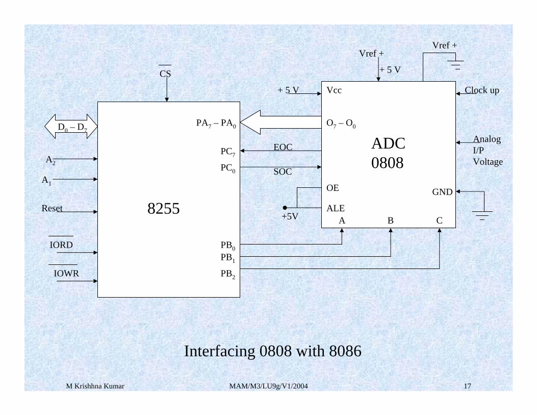
M Krishhna Kumar MAM/M3/LU9g/V1/2004 17
Interfacing 0808 with 8086
CS
D0 – D7
8255
ADC 0808
Vref +
Clock up
Analog I/P Voltage
CA B
GND
ALE
OE
+5V
EOC
SOC
Vref +
+ 5 V
+ 5 V Vcc
O7 – O0
A2
A1
Reset
IORD
IOWR PB2
PB1
PB0
PA7 – PA0
PC7
PC0

M Krishhna Kumar MAM/M3/LU9g/V1/2004 18
Interfacing Digital To Analog Converters (cont..)
INTERFACING DIGITAL TO ANALOG CONVERTERS: The digital to analog converters convert binary number into their equivalent voltages. The DAC find applications in areas like digitally controlled gains, motors speed controls, programmable gain amplifiers etc.
AD 7523 8-bit Multiplying DAC : This is a 16 pin DIP, multiplying digital to analog converter, containing R-2R ladder for D-A conversion along with single pole double thrown NMOS switches to connect the digital inputs to the ladder.

M Krishhna Kumar MAM/M3/LU9g/V1/2004 19
OUT 1
OUT 2
GND
MSB B1
B2
B3
B4
B5 B6
B7
B8
RFB
Vref in
V +
NC
NC
LSB
AD 7523
1
2
3
4
5
6
7
8
16
15
14
13
12
11
10
9
Pin Diagram of AD 7523

M Krishhna Kumar MAM/M3/LU9g/V1/2004 20
2R
R2 R4 R6 R8
2R2R2R2R2R R1 R3 R5R7
D1 D2 D3D0
+
-V0
+5V(MSB)
LSB
Fig:
Interfacing Analog to Digital Data Converters (cont..)

M Krishhna Kumar MAM/M3/LU9g/V1/2004 21
• The pin diagram of AD7523 is shown in fig the supply range is from +5V to +15V, while Vref may be any where between -10V to +10V. The maximum analog output voltage will be any where between -10V to +10V, when all the digital inputs are at logic high state.
• Usually a zener is connected between OUT1 and OUT2 to save the DAC from negative transients. An operational amplifier is used as a current to voltage converter at the output of AD to convert the current out put of AD to a proportional output voltage.
Interfacing Digital To Analog Converters (cont..)

M Krishhna Kumar MAM/M3/LU9g/V1/2004 22
• It also offers additional drive capability to the DAC output. An external feedback resistor acts to control the gain. One may not connect any external feedback resistor, if no gain control is required.
• EXAMPLE: Interfacing DAC AD7523 with an 8086 CPU running at 8MHZ and write an assembly language program to generate a sawtooth waveform of period 1ms with Vmax 5V.
• Solution: Fig shows the interfacing circuit of AD 74523 with 8086 using 8255. program gives an ALP to generate a sawtooth waveform using circuit.
Interfacing Digital To Analog Converters (cont..)

M Krishhna Kumar MAM/M3/LU9g/V1/2004 23
ASSUME CS:CODECODE SEGMENTSTART: MOV AL,80h ;make all ports output
OUT CW, ALAGAIN: MOV AL,00h ;start voltage for rampBACK : OUT PA, AL
INC ALCMP AL, 0FFhJB BACKJMP AGAINCODE ENDSEND START
Example (cont..)

M Krishhna Kumar MAM/M3/LU9g/V1/2004 24
MSB
LSBV0
8255A
CS
+
-
AD7523
GND
+5V +10V
VZ
OUT1
OUT2
RFB
3
11
4 1
2
16
1415
PA0
PA7
Fig: Interfacing of AD7523

M Krishhna Kumar MAM/M3/LU9g/V1/2004 25
• In the above program, port A is initialized as the output port for sending the digital data as input to DAC. The ramp starts from the 0V (analog), hence AL starts with 00H. To increment the ramp, the content of AL is increased during each execution of loop till it reaches F2H.
• After that the saw tooth wave again starts from 00H, i.e. 0V(analog) and the procedure is repeated. The ramp period given by this program is precisely 1.000625 ms. Here the count F2H has been calculated by dividing the required delay of 1ms by the time required for the execution of the loop once. The ramp slope can be controlled by calling a controllable delay after the OUT instruction.
Interfacing Analog to Digital Data Converters (cont..)