Embed Size (px)
Citation preview
1
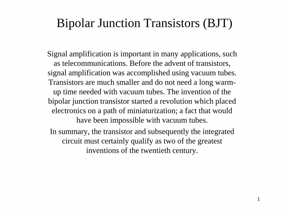
Bipolar Junction Transistors (BJT)
Signal amplification is important in many applications, such
as telecommunications. Before the advent of transistors,
signal amplification was accomplished using vacuum tubes.
Transistors are much smaller and do not need a long warm-
up time needed with vacuum tubes. The invention of the
bipolar junction transistor started a revolution which placed
electronics on a path of miniaturization; a fact that would
have been impossible with vacuum tubes.
In summary, the transistor and subsequently the integrated
circuit must certainly qualify as two of the greatest
inventions of the twentieth century.
2
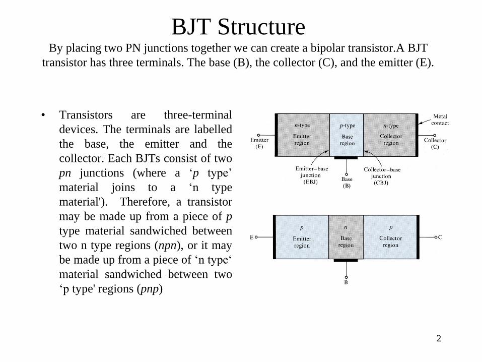
BJT Structure By placing two PN junctions together we can create a bipolar transistor.A BJT
transistor has three terminals. The base (B), the collector (C), and the emitter (E).
• Transistors are three-terminal
devices. The terminals are labelled
the base, the emitter and the
collector. Each BJTs consist of two
pn junctions (where a ‘p type’
material joins to a ‘n type
material'). Therefore, a transistor
may be made up from a piece of p
type material sandwiched between
two n type regions (npn), or it may
be made up from a piece of ‘n type‘
material sandwiched between two
‘p type' regions (pnp)
3
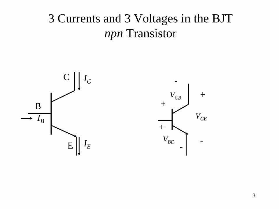
3 Currents and 3 Voltages in the BJT
npn Transistor
B
C
IB
E IE
IC
VBE
+
-
VCB
+
-
VCE
+
-
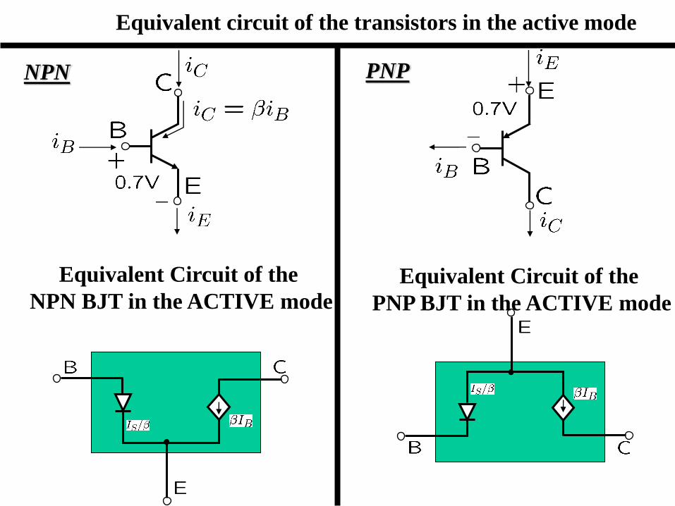
Equivalent Circuit of the
NPN BJT in the ACTIVE mode
NPN PNP
Equivalent Circuit of the
PNP BJT in the ACTIVE mode
Equivalent circuit of the transistors in the active mode
5
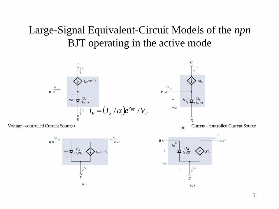
Large-Signal Equivalent-Circuit Models of the npn
BJT operating in the active mode
T
v
SE VeIi BE //
SourceCurrent controlled-CurrentSourceCurrent controlled-Voltage
6
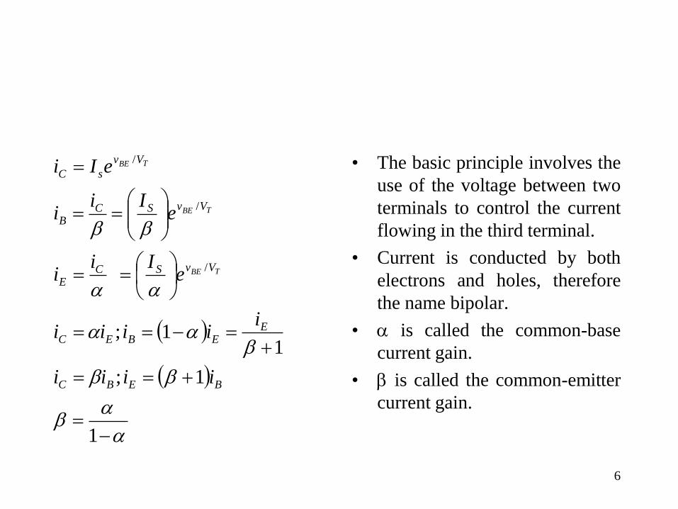
• The basic principle involves the
use of the voltage between two
terminals to control the current
flowing in the third terminal.
• Current is conducted by both
electrons and holes, therefore
the name bipolar.
• is called the common-base
current gain.
• is called the common-emitter
current gain.
1
1;
11;
/
/
/
BEBC
EEBEC
VvSCE
VvSCB
Vv
sC
iiii
iiiii
eIi
i
eIi
i
eIi
TBE
TBE
TBE
7
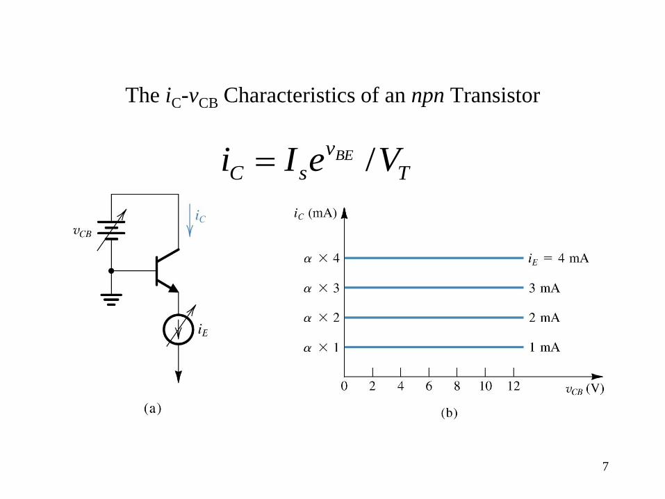
The iC-vCB Characteristics of an npn Transistor
T
v
sC VeIi BE /
8
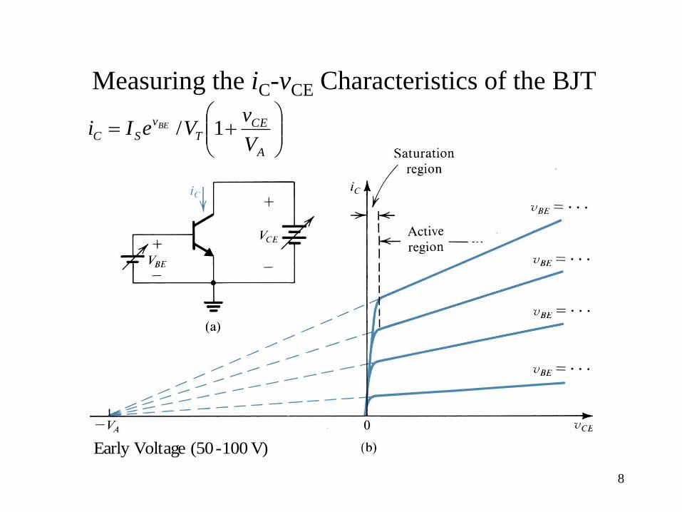
Measuring the iC-vCE Characteristics of the BJT
A
CET
v
SCV
vVeIi BE 1/
V) 100-(50 VoltageEarly
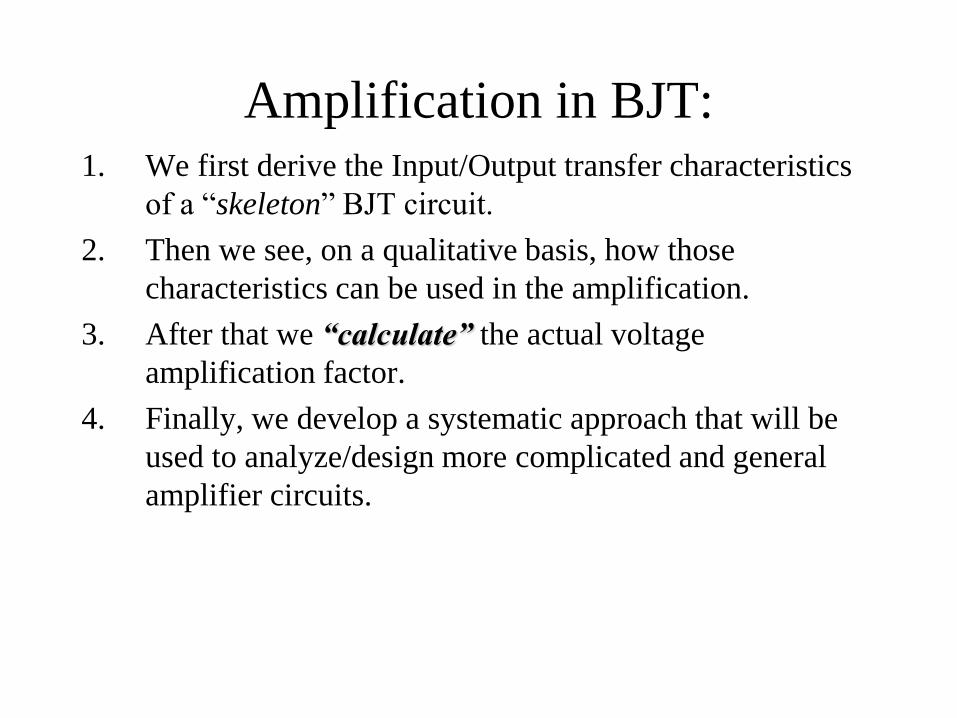
Amplification in BJT: 1. We first derive the Input/Output transfer characteristics
of a “skeleton” BJT circuit.
2. Then we see, on a qualitative basis, how those
characteristics can be used in the amplification.
3. After that we “calculate” the actual voltage
amplification factor.
4. Finally, we develop a systematic approach that will be
used to analyze/design more complicated and general
amplifier circuits.
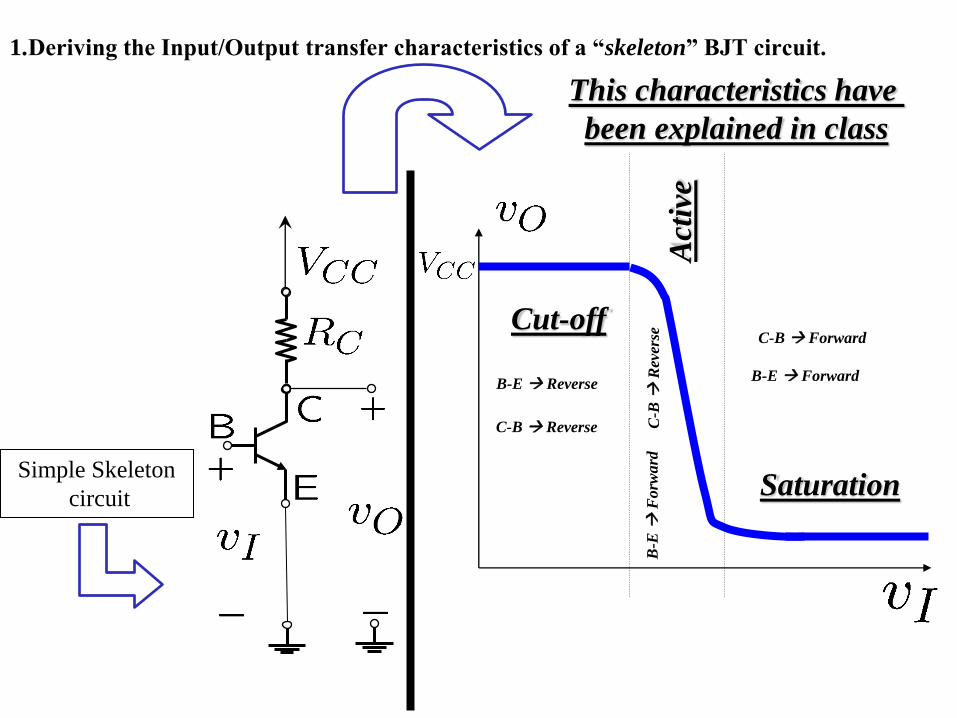
1.Deriving the Input/Output transfer characteristics of a “skeleton” BJT circuit.
Simple Skeleton
circuit
Cut-off
Act
ive
Saturation
B-E Reverse
C-B Reverse
B-E
F
orw
ard
C
-B
Rev
erse
B-E Forward
C-B Forward
This characteristics have
been explained in class
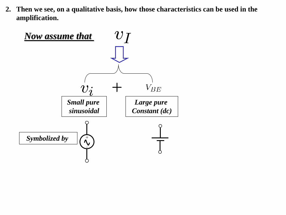
2. Then we see, on a qualitative basis, how those characteristics can be used in the
amplification.
Now assume that
Small pure
sinusoidal
Large pure
Constant (dc)
Symbolized by
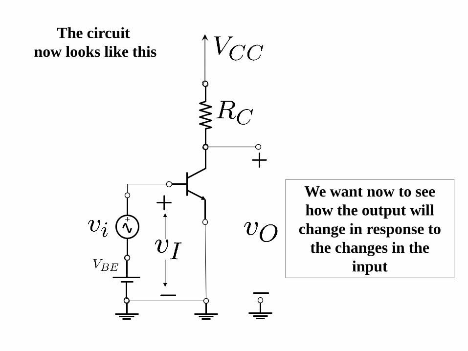
The circuit
now looks like this
We want now to see
how the output will
change in response to
the changes in the
input
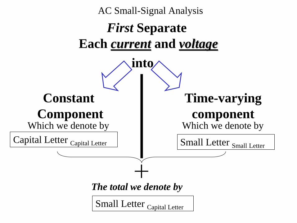
AC Small-Signal Analysis
First Separate
Each current and voltage
Constant
Component
Time-varying
component
into
Small Letter Small Letter Capital Letter Capital Letter
Which we denote by Which we denote by
The total we denote by
Small Letter Capital Letter
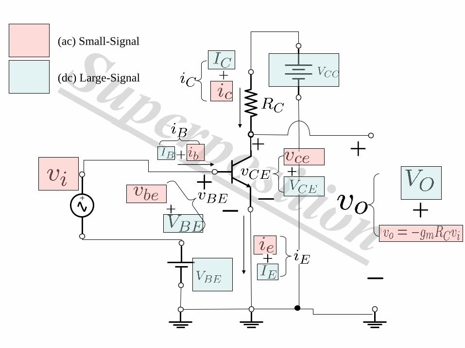
(dc) Large-Signal
(ac) Small-Signal
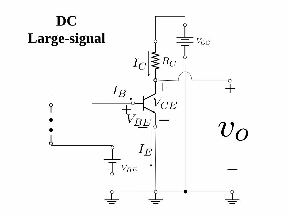
DC
Large-signal
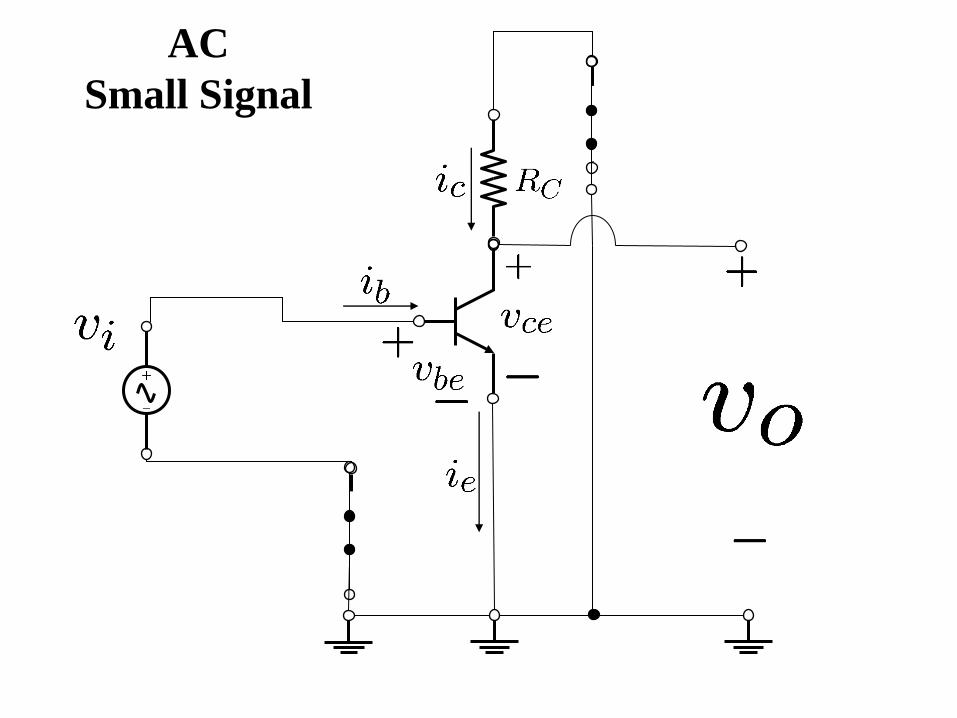
AC
Small Signal