Embed Size (px)
Citation preview
Bipolar Junction Transistors (BJT)
04/19/23 www.noteshit.com 1
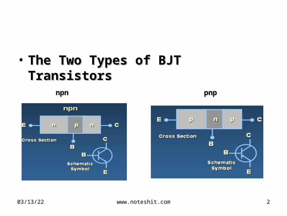
• The Two Types of BJT TransistorsThe Two Types of BJT Transistors
npnnpn pnppnp
04/19/23 www.noteshit.com 2
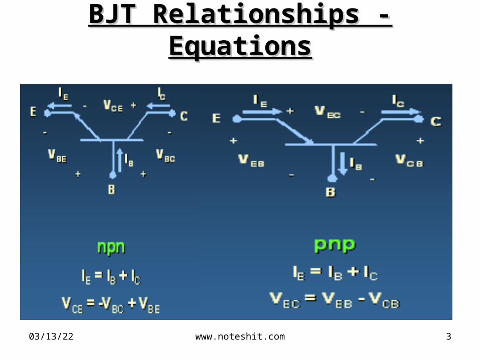
BJT Relationships - EquationsBJT Relationships - Equations
04/19/23 www.noteshit.com 3
= Common-emitter current gain= Common-emitter current gain = Common-base current gain= Common-base current gain = IC= IC = IC = IC IBIB IE IE
The relationships between the two parameters are:The relationships between the two parameters are: = = = = + 1+ 1 1 - 1 -
Note: Note: and and are sometimes referred to as are sometimes referred to as dc and dc and dc dc because the relationships being dealt with in because the relationships being dealt with in the BJT the BJT are DC.are DC.
DC DC and DC and DC
04/19/23 www.noteshit.com 4
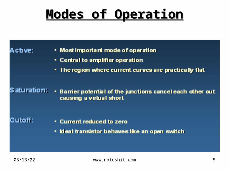
Modes of OperationModes of Operation
04/19/23 www.noteshit.com 5
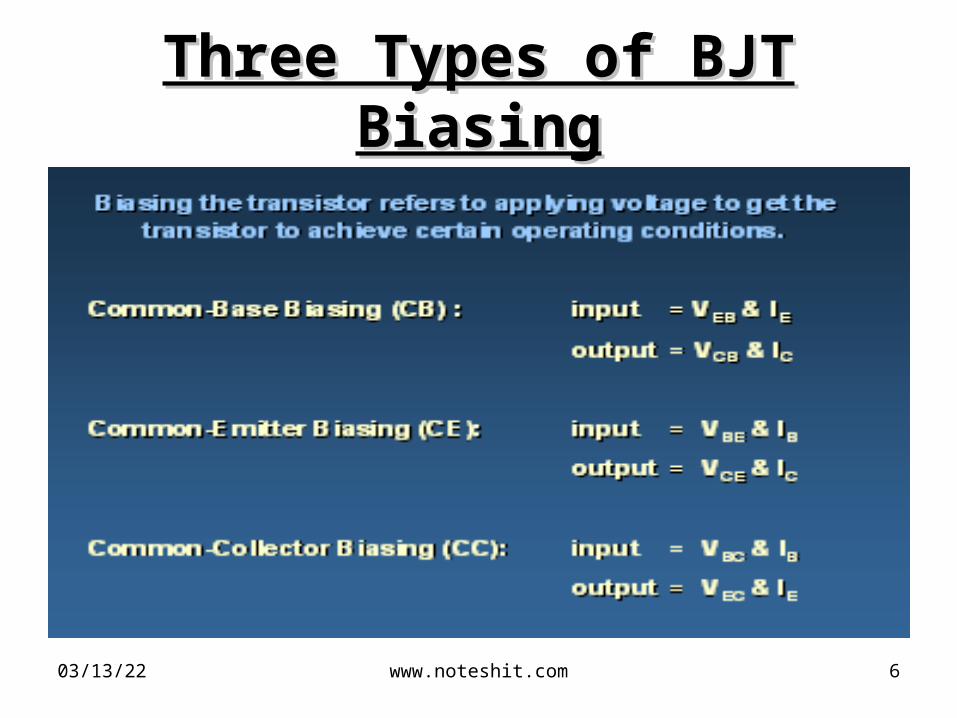
Three Types of BJT BiasingThree Types of BJT Biasing
04/19/23 www.noteshit.com 6
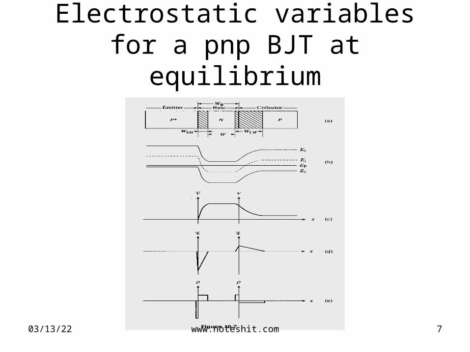
Electrostatic variables for a pnp BJT at equilibrium
04/19/23 www.noteshit.com 7
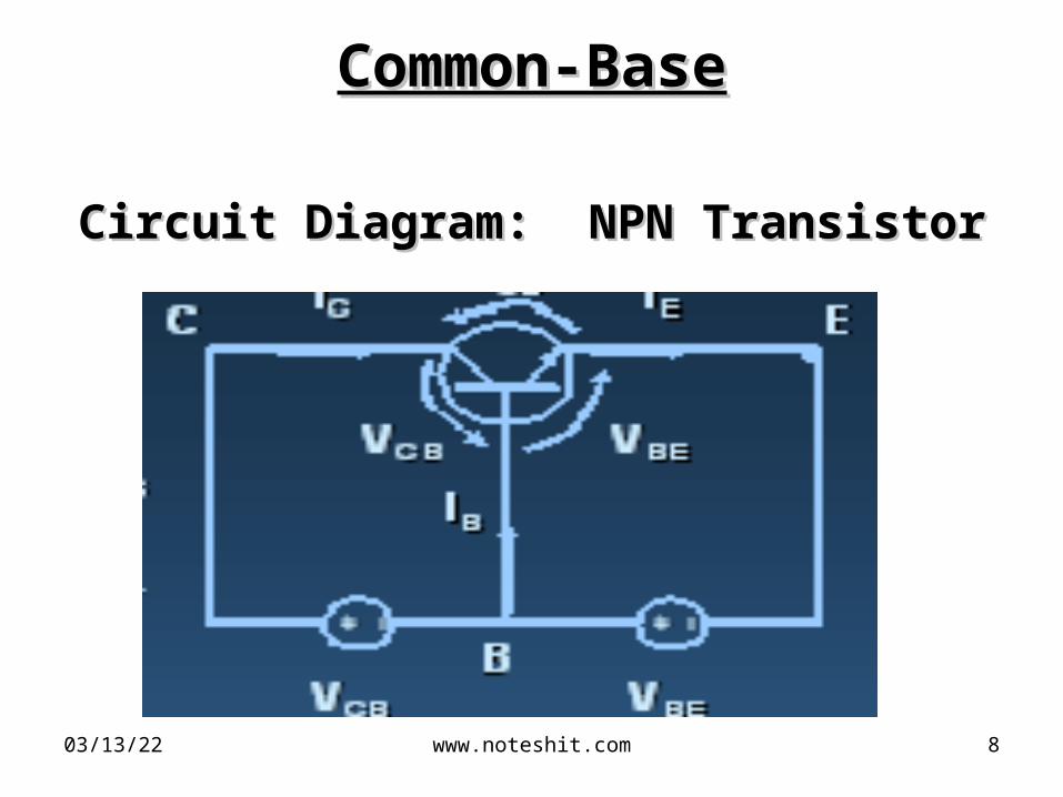
Common-BaseCommon-Base
Circuit Diagram: NPN TransistorCircuit Diagram: NPN Transistor
04/19/23 www.noteshit.com 8
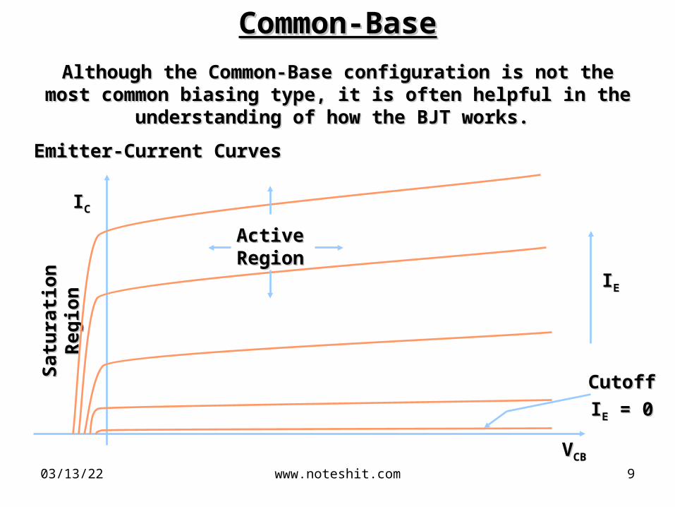
Common-BaseCommon-Base
Although the Common-Base configuration is not the most Although the Common-Base configuration is not the most common biasing type, it is often helpful in the understanding of common biasing type, it is often helpful in the understanding of
how the BJT works. how the BJT works.
Emitter-Current CurvesEmitter-Current Curves
Sa
tura
tio
n R
egio
nS
atu
rati
on
Reg
ion
IIEE
IICC
VVCBCB
Active Active RegionRegion
CutoffCutoff
IIEE = 0 = 0
04/19/23 www.noteshit.com 9
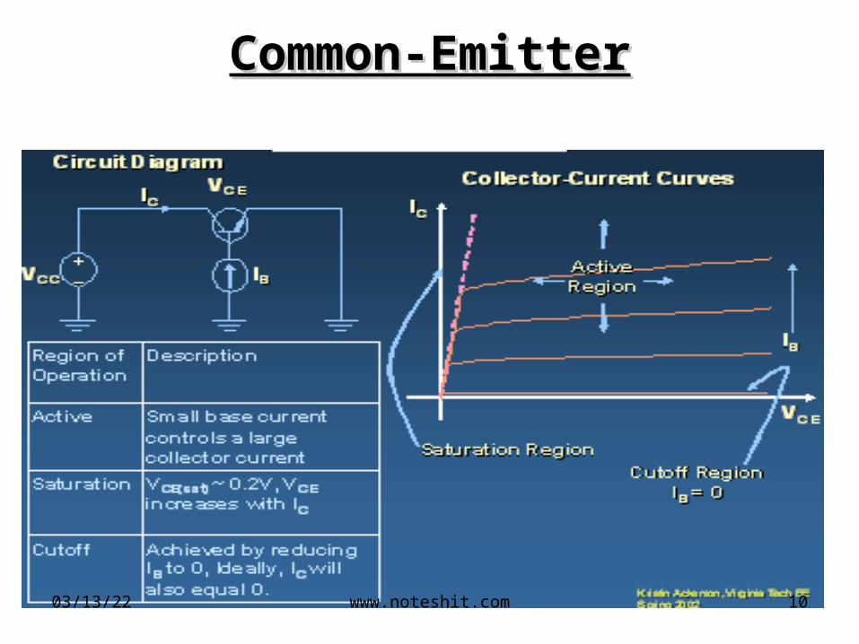
Common-EmitterCommon-Emitter
04/19/23 www.noteshit.com 10
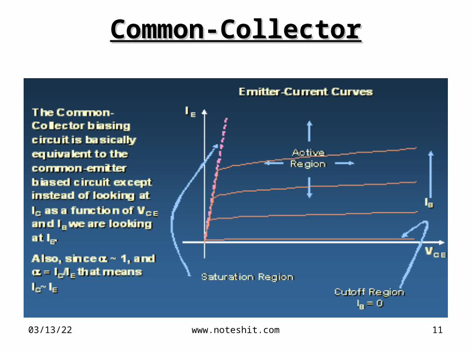
Common-CollectorCommon-Collector
04/19/23 www.noteshit.com 11
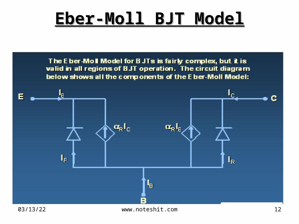
Eber-Moll BJT ModelEber-Moll BJT Model
04/19/23 www.noteshit.com 12
Common-emitter transistor
• Common-emitter transistor ampliers are so-called because the input and output voltage points share the emitter lead of the transistor in common with each other, not considering any power supplies.
• ² Transistors are essentially DC devices: they cannot directly handle voltages or currents that reverse direction. In order to make them work for amplifying AC signals, the input signal must be offset with a DC voltage to keep the transistor in its active mode throughout the entire cycle of the wave. This is called biasing.
04/19/23 www.noteshit.com 13
Common-collector transistor
• Common-collector transistor ampliers are so-called because the input and output voltage points share the collector lead of the transistor in common with each other, not considering any power supplies.
• ² The output voltage on a common-collector amplier will be in phase with the input voltage, making the common-collector a non-inverting amplier circuit.
• ² The current gain of a common-collector amplier is equal to Ø plus 1. The voltage gain is approximately equal to 1 (in practice, just a little bit less).
04/19/23 www.noteshit.com 14
Common-base transistor
• Common-base transistor ampliers are so-called because the input and output voltage points share the base lead of the transistor in common with each other, not considering any power supplies.
• ² The current gain of a common-base amplier is always less than 1. The voltage gain is a function of input and output resistances, and also the internal resistance of the emitterbase junction, which is subject to change with variations in DC bias voltage.
04/19/23 www.noteshit.com 15
TRANSISTOR MODEL
• Common-Base Configuration
Common-base BJT transistorre modelre equivalent cct.
04/19/23 www.noteshit.com 16
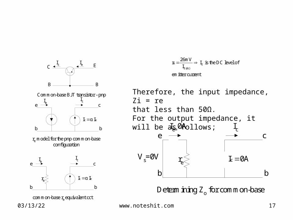
E
BB
C
Common-base BJT transistor - pnp
Ic Ie
e
b b
c
ec I αI
IcIe
re model for the pnp common-baseconfiguration
e
b b
c
ec I αI
IcIe
common-base re equivalent cct
re
Therefore, the input impedance, Zi = rethat less than 50Ω.For the output impedance, it will be as follows;
e
b b
c
A0Ic
IcIe=0A
Determining Zo for common-base
reVs=0V
e EE(dc)
26mVr I is the DC level of
I
emitter current
04/19/23 www.noteshit.com 17
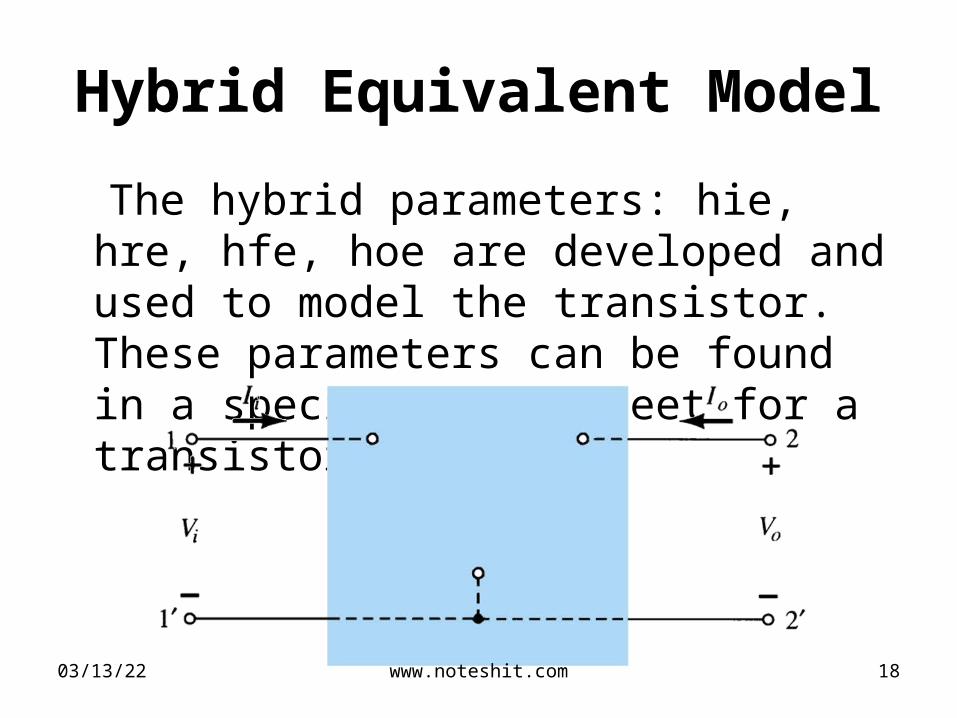
The hybrid parameters: hie, hre, hfe, hoe are developed and used to model the transistor. These parameters can be found in a specification sheet for a transistor.
Hybrid Equivalent Model
04/19/23 www.noteshit.com 18
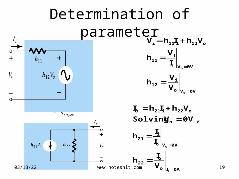
Determination of parameter
0VVo
i12
0VVi
i11
o12i11i
o
o
VV
h
IV
h
VhIhV
0AIo
o22
0VVo
i21
o
o22i21O
o
o
VI
h
II
h
, 0VV Solving
VhIhI
0VVo
i12
0VVi
i11
o12i11i
o
o
VV
h
IV
h
VhIhV
04/19/23 www.noteshit.com 19
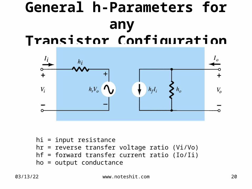
General h-Parameters for any Transistor Configuration
hi = input resistancehr = reverse transfer voltage ratio (Vi/Vo)hf = forward transfer current ratio (Io/Ii)ho = output conductance
04/19/23 www.noteshit.com 20
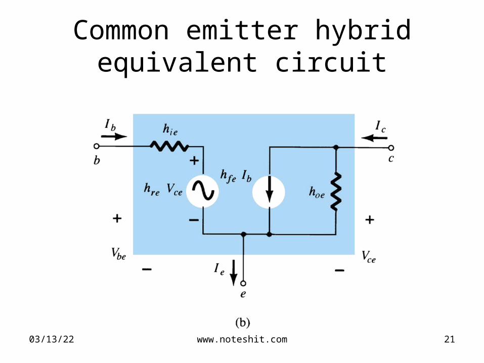
Common emitter hybrid equivalent circuit
04/19/23 www.noteshit.com 21
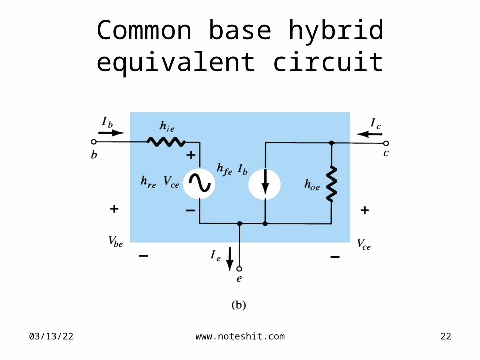
Common base hybrid equivalent circuit
04/19/23 www.noteshit.com 22
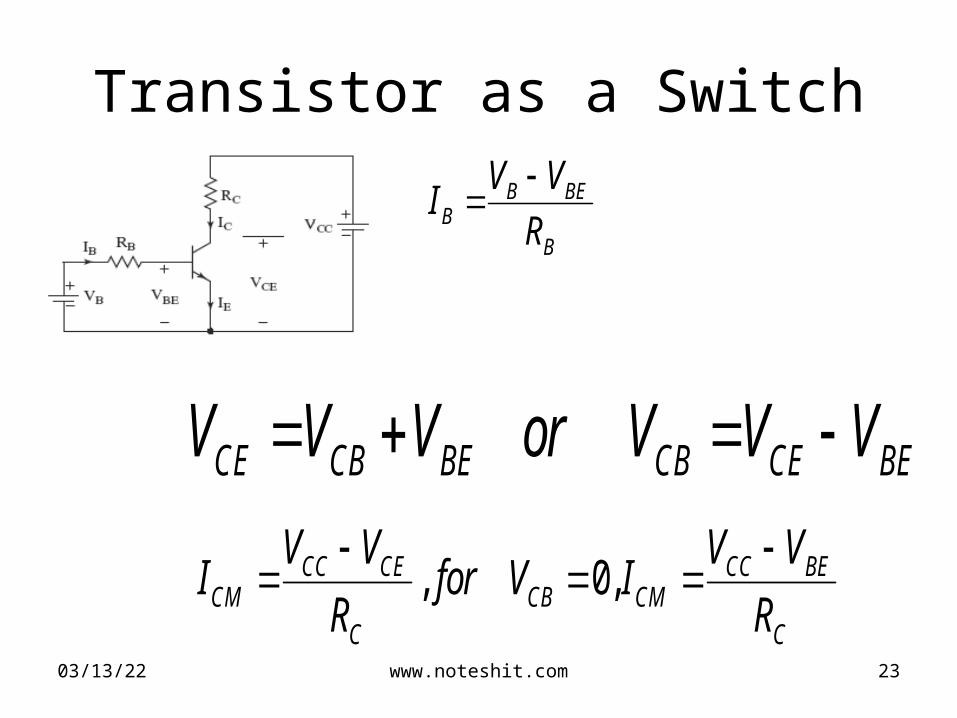
Transistor as a Switch
B BEB
B
V VI
R
CE CB BE CB CE BEV V V or V V V
, 0,CC CE CC BECM CB CM
C C
V V V VI for V I
R R
04/19/23 www.noteshit.com 23
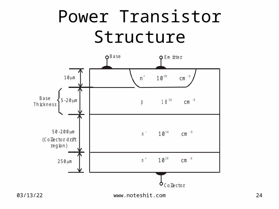
Power Transistor Structure
Em itterBase
n + 1019 cm - 3
p 1 0 16 cm - 3
n – 1014 cm - 3
n + 1019 cm - 3
Co llector
250 m
50- 200 m
10 m
5- 20 m
(C ollector driftregion)
Base Th ickness
04/19/23 www.noteshit.com 24
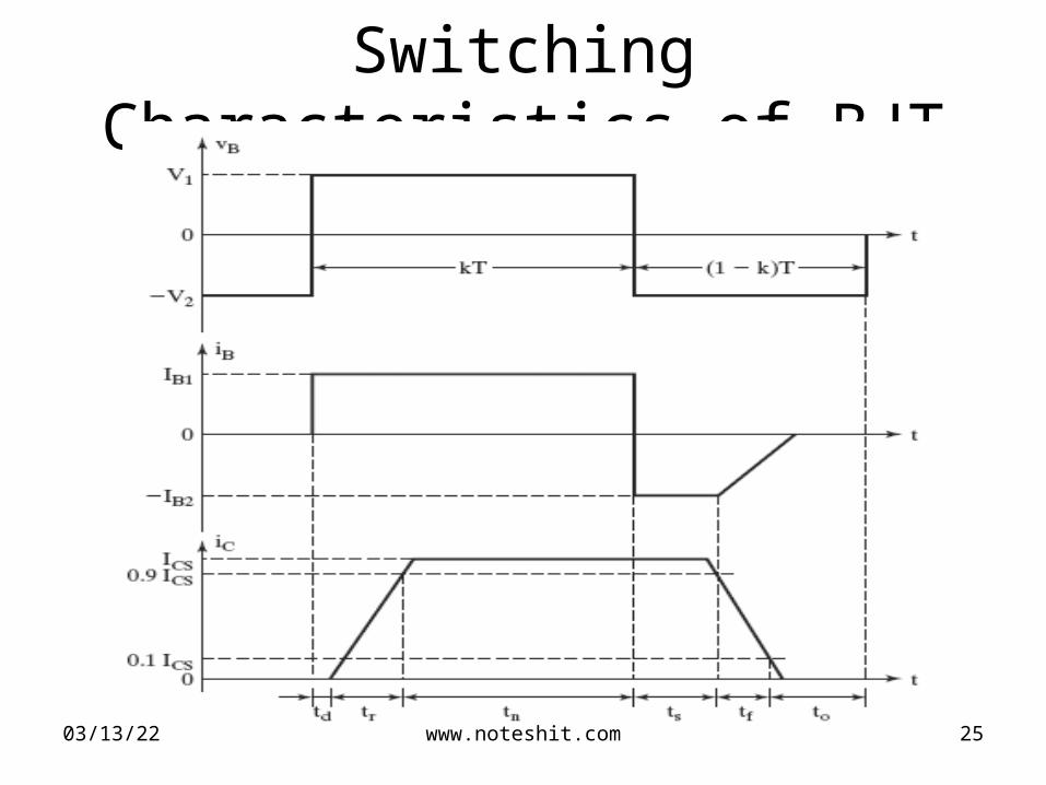
Switching Characteristics of BJT
04/19/23 www.noteshit.com 25