Embed Size (px)
Citation preview

Bipolar Junction Transistors (BJT)
NPN PNP

BJT Cross-Sections
NPN PNP
Emitter
Collector

Common-Emitter NPN Transistor
Forward bias the BEJ
Reverse bias the CBJ

Input Characteristics
• Plot IB as f(VBE, VCE)
• As VCE increases, more VBE required to turn the BE on so that IB>0.
• Looks like a pn junction volt-ampere characteristic.
Output Characteristics
• Plot IC as f(VCE, IB)• Cutoff region (off)
– both BE and BC reverse biased
• Active region– BE Forward biased– BC Reverse biased
• Saturation region (on)– both BE and BC
forward biased

Transfer Characteristics

Large-Signal Model of a BJT
KCL >> IE = IC + IB
βF = hFE = IC/IB
IC = βFIB + ICEO
IE = IB(1 + βF) + ICEO
IE = IB(1 + βF)
IE = IC(1 + 1/βF)
IE = IC(βF + 1)/βF

(1 ) ( 1)
111
1 1
E B C
CF FE
B
C F B CEO
E B F CEO B F
FE C C
F F
C F E
F FF F
F F
I I I
Ih
I
I I I
I I I I
I I I
I I

Transistor Operating Point
B BEB
B
CE CCC
C C
CE CC C C
V VI
R
V VI
R R
V V I R

DC Load Line
VCC
VCC/RC

BJT Transistor Switch
B BEB
B
CE CC C C
CE CB BE
CB CE BE
V VI
R
V V I R
V V V
V V V

BJT Transistor Switch (continued)
CC CE CC BECM
C C
CMBM
F
V V V VI
R R
II

BJT in Saturation
( )CC CE satCS
C
CSBS
F
B
BS
CSforced
B
V VI
R
II
IODF
I
I
I

Model with Current Gain

Miller Effect
vbe vce
iout

Miller Effect (continued)
( ) ( )
[1 ] [1 ]
[1 ]
out cb be ce cb be be
out cb be cb be
cb cb
d di C v v C v Av
dt dtd d
i C A v C A vdt dt
C C A

Miller Effect (continued)
• Miller Capacitance, CMiller = Ccb(1 – A)
– since A is usually negative (phase inversion), the Miller capacitance can be much greater than the capacitance Ccb
• This capacitance must charge up to the base-emitter forward bias voltage, causing a delay time before any collector current flows.
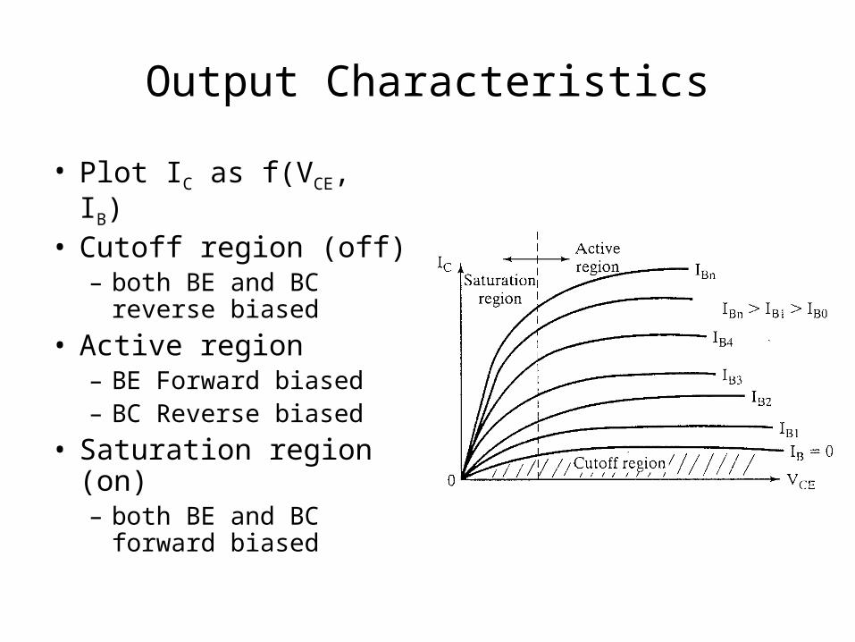
Saturating a BJT
• Normally apply more base current than needed to saturate the transistor
• This results in charges being stored in the base region
• To calculate the extra charge (saturating charge), determine the emitter current
1cse B BS BS BS
II I ODF I I I ODF

The Saturating Charge
• The saturating charge, Qs
( 1)s s e s BSQ I I ODF
storage time constant of the transistor

Transistor Switching Times

Switching Times – turn on
• Input voltage rises from 0 to V1
• Base current rises to IB1
• Collector current begins to rise after the delay time, td
• Collector current rises to steady-state value ICS
• This “rise time”, tr allows the Miller capacitance to charge to V1
• turn on time, ton = td + tr

Switching Times – turn off
• Input voltage changes from V1 to –V2
• Base current changes to –IB2
• Base current remains at –IB2 until the Miller capacitance discharges to zero, storage time, ts
• Base current falls to zero as Miller capacitance charges to –V2, fall time, tf
• turn off time, toff = ts + tf

Charge Storage in Saturated BJTs
Charge storage in the Base Charge Profile during turn-off

Example 4.2

Waveforms for the Transistor Switch
VCC = 250 V
VBE(sat) = 3 V
IB = 8 A
VCS(sat) = 2 V
ICS = 100 A
td = 0.5 µs
tr = 1 µs
ts = 5 µs
tf = 3 µs
fs = 10 kHz
duty cycle k = 50 %
ICEO = 3 mA

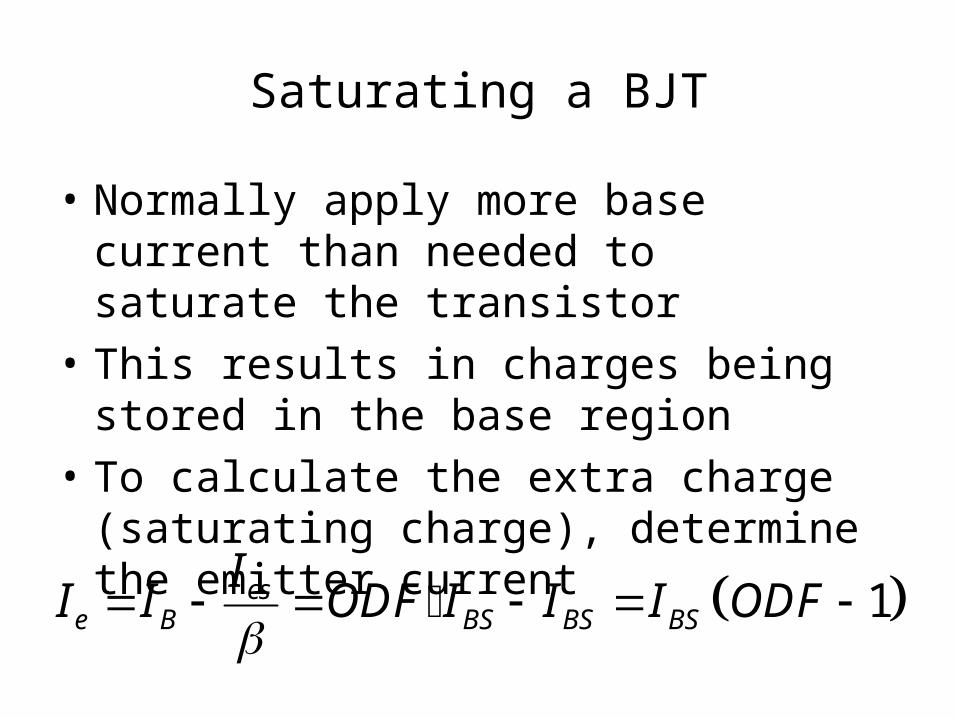
Power Loss due to IC for ton = td + tr
• During the delay time, 0 ≤t ≤td
• Instantaneous Power Loss
• Average Power Loss
0 0
1( )
(250 )(3 )(10 )(0.5 ) 3.75
d dt t
CC CEOd c CC CEO s d
d
V IP P t dt dt V I f t
T T
P V mA kHz s mW
( )
( ) (250 )(3 ) 0.75c CE C CC CEO
c
P t v i V I
P t V mA W

During the rise time, 0 ≤t ≤tr
( )
( )( )
max
( )
( )
( ) ( )
( )( )
( ) @
2[ ]
c CE c
CSc CC ce sat CC
r r
ce sat CCc CS CSCC ce sat CC
r r r r
c m
r CCm
CC ce sat
P t v i
ItP t V V V t
t t
V VdP t I Itt V V V
dt t t t t
P t P t t
t Vt
V V

2
max( )
2
max
(1 )(250 )0.504
2[250 2 ]
4[ ]
(250 ) (100 )6300
4[250 2 ]
m
CC CS
CC CE sat
s Vt s
V V
V IP
V V
V AP W
V V

Average Power during rise time
( )
0
1( )
2 3
(250 ) (2 250 )(10 )(100 )(1 )
2 3
42.33
rtCE sat CCCC
r c s CS r
r
r
V VVP P t dt f I t
T
V V VP kHz A s
P W

Total Power Loss during turn-on
0.00375 42.33 42.33375
42.33
on d r
on
on
P P P
P W
P W


Power Loss during the Conduction Period
( )
( ) ( )
0 0
0
( ) 100
( ) 2
( ) (100 )(2 ) 200
1( )
(2 )(100 )(10 )(48.5 ) 97
n n
n
c CS
CE CE sat
c c CE
t t
n c CE sat CS s CE sat CS s n
n
t t
i t I A
v t V V
P t i v A V W
P P t dt V I f dt V I f tT
P V A kHz s W


Power Loss during turn offStorage time
( )
( )
( ) ( )
0 0
0
( ) 100
( ) 2
( ) (2 )(100 )
( ) 200
1( )
(2 )(100 )(10 )(5 ) 10
s s
s
c CS
CE CE sat
c CE c CE sat CS
c
t t
s c CE sat CS s CE sat CS s s
s
t t
i t I A
v t V V
P t v i V I V A
P t W
P P t dt V I f dt V I f tT
P V A kHz s W


Power Loss during Fall time0
( ) 1 , 0
( ) , 0
( ) 1
( ) 11 0
3( ) @ 1.5
2 2(250 )(100 )
4 4
f
c CS CEOf
CCCE CEO
f
c CE c CC CSf f
c CC CS
f f f
fc m
CC CSm
t t
ti t I I
t
Vv t t I
t
t tP t v i V I
t t
dP t V I tt
dt t t t
t sP t P t s
V I V AP
6250W

Power Loss during Fall time (continued)
0
( )
1( )
6
(250 )(100 )(3 )(10 )125
6
6
10 125 135
ftCC CS f s
f c
f
CC foff s f CS s s CE sat
off
V I t fP P t dt
T
V A s kHzP W
V tP P P I f t V
P W


Power Loss during the off time
0
0
( )
( )
( ) (250 )(3 ) 0.75
1
(250 )(3 )(10 )((50 5 3) )
0.315
o
o
CE CC
c CEO
c CE C CC CEO
t
o CC CEO CC CEO s o
o
o
t t
v t V
i t I
P t v i V I V mA W
P V I dt V I f tT
P V mA kHz s
P W
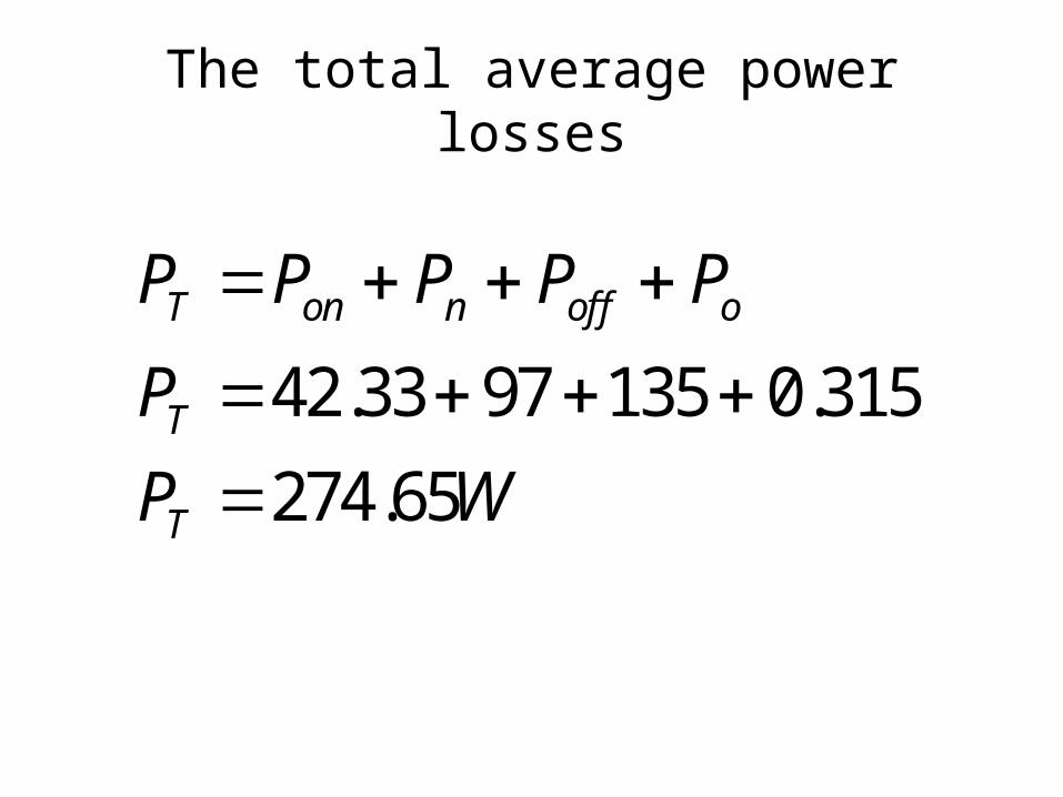
The total average power losses
42.33 97 135 0.315
274.65
T on n off o
T
T
P P P P P
P
P W

Instantaneous Power for Example 4.2

BJT Switch with an Inductive Load

Load Lines


![BJT [Modo de compatibilidad]lcr.uns.edu.ar/electronica/introducc_electr/2010/clases/...• Para un transistor NPN → • Volviendo al BJT PNP, si polarizamos la juntura BE en directa](https://img.dokumen.tips/doc/110x75/608b1c0ed906c4754a463117/bjt-modo-de-compatibilidadlcrunseduarelectronicaintroduccelectr2010clases.jpg)