Embed Size (px)
Citation preview
Analog Low Noise Amplifier Circuit Design
and Optimization
Ph.D. Synopsis
Submitted
To
Gujarat Technological University, Ahmedabad
For The Degree
of
Doctor of Philosophy
In
Electronics & Communication Engineering
By
Hasmukh P Koringa
Enrollment No: 119997111005
(Electronics & Communication Engineering)
Supervisor:
Dr. Vipul A Shah, Professor and Head, IC Department,
Faculty Of Technology, Dharmsinh Desai University,
Nadiad, India.
Co-Supervisor:
Prof. Durgamadhab Misra, Professor,
Electrical Engineering Department,
New Jersey Institute of Technology, New Jersey,
USA.
2
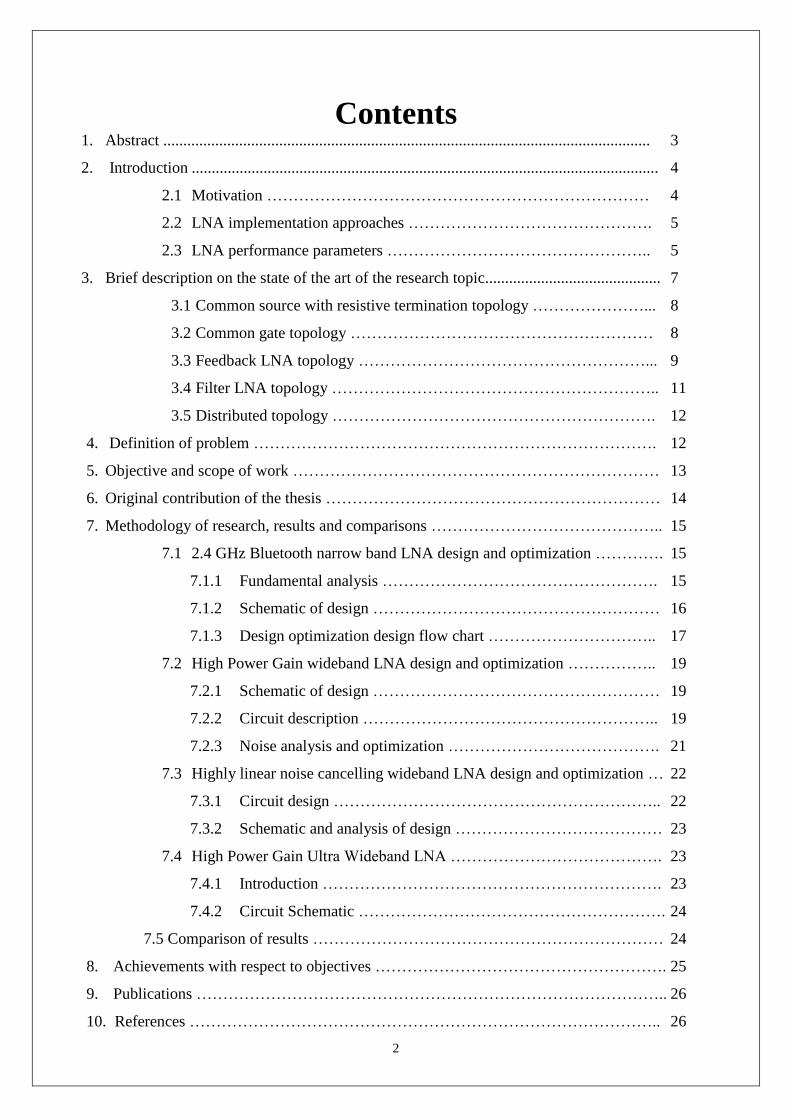
Contents 1. Abstract .......................................................................................................................... 3
2. Introduction ..................................................................................................................... 4
2.1 Motivation ……………………………………………………………… 4
2.2 LNA implementation approaches ………………………………………. 5
2.3 LNA performance parameters ………………………………………….. 5
3. Brief description on the state of the art of the research topic............................................ 7
3.1 Common source with resistive termination topology …………………... 8
3.2 Common gate topology ………………………………………………… 8
3.3 Feedback LNA topology ………………………………………………... 9
3.4 Filter LNA topology …………………………………………………….. 11
3.5 Distributed topology ……………………………………………………. 12
4. Definition of problem …………………………………………………………………. 12
5. Objective and scope of work …………………………………………………………… 13
6. Original contribution of the thesis ……………………………………………………… 14
7. Methodology of research, results and comparisons …………………………………….. 15
7.1 2.4 GHz Bluetooth narrow band LNA design and optimization …………. 15
7.1.1 Fundamental analysis ……………………………………………. 15
7.1.2 Schematic of design ……………………………………………… 16
7.1.3 Design optimization design flow chart ………………………….. 17
7.2 High Power Gain wideband LNA design and optimization …………….. 19
7.2.1 Schematic of design ……………………………………………… 19
7.2.2 Circuit description ……………………………………………….. 19
7.2.3 Noise analysis and optimization …………………………………. 21
7.3 Highly linear noise cancelling wideband LNA design and optimization … 22
7.3.1 Circuit design …………………………………………………….. 22
7.3.2 Schematic and analysis of design ………………………………… 23
7.4 High Power Gain Ultra Wideband LNA …………………………………. 23
7.4.1 Introduction ………………………………………………………. 23
7.4.2 Circuit Schematic …………………………………………………. 24
7.5 Comparison of results ………………………………………………………… 24
8. Achievements with respect to objectives ………………………………………………. 25
9. Publications …………………………………………………………………………….. 26
10. References …………………………………………………………………………….. 26

3
1. Abstract
With the increasing use of wireless communications, there emerges a trend towards
integrating multiple wireless functionalities into one mobile device. Recently we have been
observing a paradigm shift in the integrated wireless transceiver design where several
narrow-band receivers customized for dedicated applications, e.g. cellular, wireless LAN
(Local Area Network), and PAN (Personal Area Network) are replaced by one single circuit
which support different standards operating on different frequency band is called ―Universal
Receiver‖. To support multiple standards which have different modulation techniques put
tough performance requirement for noise, gain and matching of universal receiver design.
Realizing Analog to digital converter for universal receiver for the RF signal without Low
Noise Amplifier (LNA) is practically very difficult using current technology. The LNA and
mixer are relaxing the stringent performance requirements of the analog to digital converter.
In LNA design has performance trade-off among noise, gain, linearity, matching and power
consumption. In the research designed and proposed two narrowband LNAs and three
wideband LNAs for the Bluetooth, GPS, UWB and 4G technologies. Detailed analysis of all
LNAs are carried out. All the LNAs design using 0.18µm RFCMOS model and simulate the
design using Advanced Design System RF circuit simulator software.
4
2. Introduction
2.1 Motivation
The demand of wireless transceiver RFICs is exp expanding rapidly because of its huge
market ranging from pagers, cordless phones, cell phones, WLAN terminals, nodes for sensor
networks and GPS to recently introduced DAB/DVB enabled PDAs [1]. These diverse range
of mobile terminals have their own standard and require separate RF front-end and digital
resources for baseband processing. As per today’s demand modern mobile terminals should
support WLAN, Bluetooth, ZigBee, GSM, 3G, GPS, LTE, IEEE 802.11a/b/g and WiMax etc.
wireless communication standards. This demands the mobile terminals to be flexible in
nature with low power and low cost.
Therefore, the designer is urged to integrate all radio blocks on a single chip along with
hardware reuse/sharing which not only results in cost reduction due to reduced silicon area
but allows exclusion of separate RF packaged chips at the same time. On-chip integration and
placing a lower limit on the power consumption of performance centric analog circuits helps
to reduce the power consumption [2] .
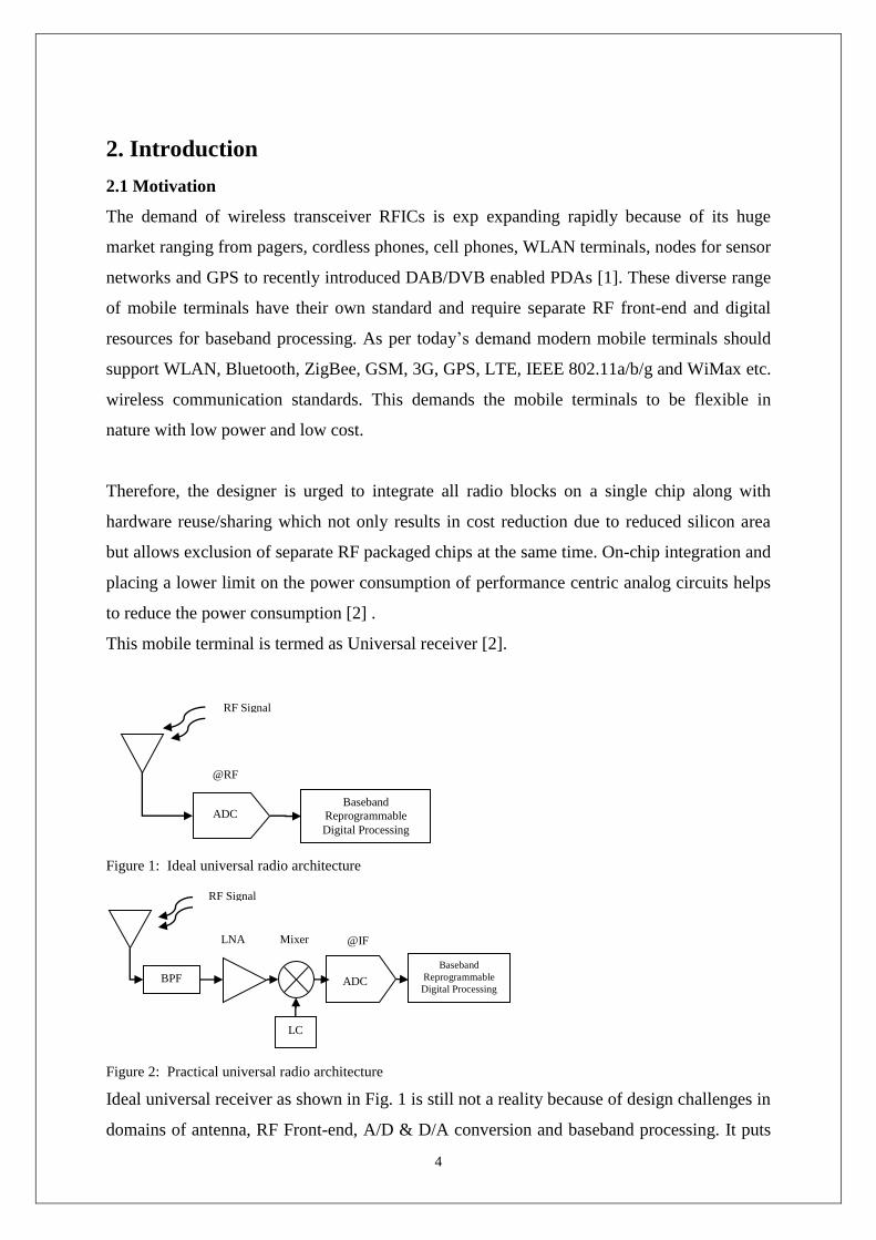
This mobile terminal is termed as Universal receiver [2].
Figure 1: Ideal universal radio architecture
Figure 2: Practical universal radio architecture
Ideal universal receiver as shown in Fig. 1 is still not a reality because of design challenges in
domains of antenna, RF Front-end, A/D & D/A conversion and baseband processing. It puts
RF Signal
ADC
@RF
Baseband
Reprogrammable
Digital Processing
BPF
RF Signal
LC
ADC
@IF LNA Mixer
Baseband
Reprogrammable
Digital Processing
5
very tough requirements on the dynamic range, speed, noise performance and linearity of
A/D converter. An LNA relaxes the noise performance and dynamic range requirements
while the frequency translation block reduces the speed requirements of the A/D converter.
That is why, all multistandard, multiband receiver designs reported to date incorporate some
sort of low noise amplifier.
The design specifications of next generation wideband LNAs should have S11≤−10 dB, NF≤
3.5 dB, IIP3≥-5 dBm, Flat gain across the entire bandwidth and unconditional stability over
entire frequency range [8,6,7,13]. These requirements must be fulfilled without any
compromise on silicon area and power consumption compared to narrowband LNAs, making
them suitable for portable and hand-held applications [53].
2.2 LNA implementation approaches
Multi band multi mode LNA to support multiple standards can be obtain using three possible
ways: (i) using a narrowband LNAs for each standard which results in high power
consumption as well as higher cost due to large Si area [54–60], (ii) using a
reconfigurable/band switching/multiband LNA. This allows more compactness and power
saving but still occupies large area because of tuning inductors [5,61,62,63–65], (iii) using
wideband LNA which allows simultaneous multiband operation with low cost and small area
[66,67,19,68,69,31,70]. Wideband LNA is good solution of accommodate multiple standards.
2.3 Low Noise Amplifier (LNA) Performance Parameters
Major performance parameters of LNA are:
a) Noise Figure (NF)
b) Power Gain (S21) and Input matching (S11)
c) Linearity (IIP3)
d) Power consumption
e) Stability
a) Noise Performance
The fundamental noise performance parameter is the Noise Factor (F), which is defined
as the ratio of the total output noise power to the output noise due to input source. If the
Noise Factor is expressed in decibels it is called the Noise Figure (NF)
NF = 10log(F)
(1)
6
⁄
⁄ (2)
A low-noise amplifier (LNA) is first amplifier stage of a receiver. Overall noise of multistage
amplifier receiver is
( )
( ) (3)
Equation (3) is also known as Friis formula which is named after the Danish-American
electrical engineer Harald T. Friis. Total receiver noise figure is dominated by the first few
stages, especially the very first stage (namely the LNA). This is the rationale behind why the
first stage amplifier needs to have as small of noise figure as possible.
b) Power gain and input matching
Other design performance parameter is Power gain (S21) it should have as high as possible to
increase weak signal received from antenna. Measure of power gain can be obtained by S
parameter S21. It is very important that the input impedance of the LNA is matched to a
certain value, most commonly 50 Ω. A measure of the quality of the input match can be
obtained by S11. If we assign the input port of an LNA to be port 1, S11 will be a complex
number representing the ratio of how much power is reflected from port 1 to how much
power is applied to port 1. So the magnitude of S11 (normally expressed in dB) is desired to
be as small as possible (S11 = -∞ for a perfect impedance match). And the reason that it
should be matched to 50 Ω is that most antennas have characteristic impedance of 50 Ω.
c) Linearity
The linearity of the LNA is another concern that must be taken into account. Linear operation
is crucial, particularly when the input signal is weak with a strong interfering signal in close
proximity. This is because in such a scenario there is a possibility for undesired inter-
modulation distortion such as blocking and cross modulation.
Third-order intercept (IP3) and 1-dB compression point (P1dB) are two measures of
linearity.IP3 shows at what power level the third-order inter-modulation product is equal to
the power of the first-order output. IIP3 and OIP3 are the input power and output power
respectively, that corresponds to IP3. P1dB shows at what power level the output power
drops 1dB, as a consequence of non-linearity, relative the theoretical linear power gain, By
knowing either IP3 or P1dB the other can be estimated with the following rule-of-thumb
formula: IIP3=p1dBm+10dBm
7
d) Power consumption
Power consumption is another design specification that needs to be closely inspected.
Considering only the noise performance and linearity can lead to biasing solution that makes
the power consumption simply too big to be practically realized. Increased incorporation of
RF systems into hand-held device makes it necessary to minimize power consumption in
order to maximize battery life.
e) Stability
In the presence of feedback paths from the output to the input, the circuit might become
unstable for certain combinations of source and load impedances. An LNA design that is
normally stable might oscillate at the extremes of the manufacturing or voltage variations,
and perhaps at unexpectedly high or low frequencies. The stability factor is given as in
| | | | | |
| || | (4)
Where, When K > 1 and < 1, the circuit is unconditionally stable.
As we can see, the design of an LNA is a multi-dimensional optimization problem. There are
lots of trade-offs involved because the optimization of each individual specification does not
arrive at the same sizing or biasing solution. This requires that the designer consider what is
the best combination of performance specifications for the intended application of the LNA.
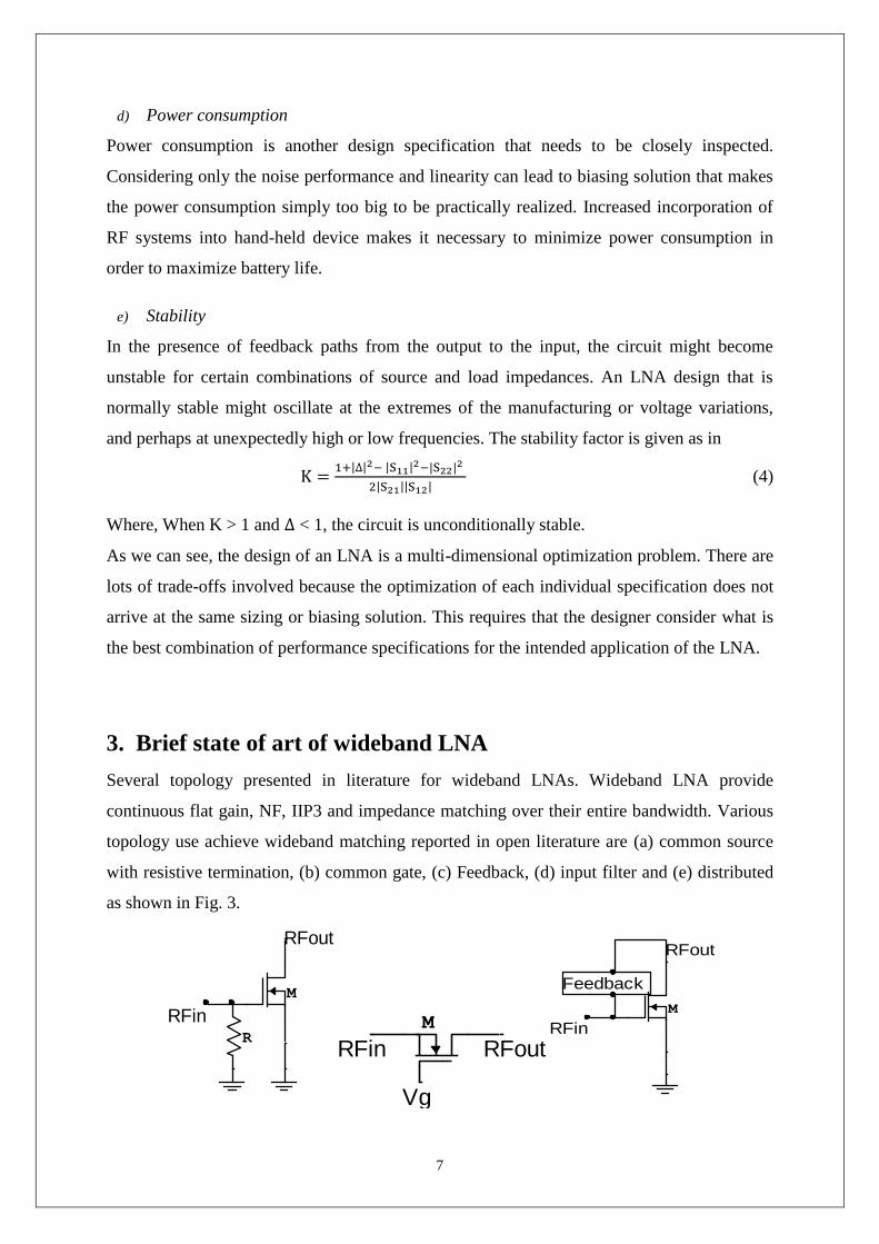
3. Brief state of art of wideband LNA
Several topology presented in literature for wideband LNAs. Wideband LNA provide
continuous flat gain, NF, IIP3 and impedance matching over their entire bandwidth. Various
topology use achieve wideband matching reported in open literature are (a) common source
with resistive termination, (b) common gate, (c) Feedback, (d) input filter and (e) distributed
as shown in Fig. 3.
M
RFin
RFout
RM
RFin RFout
Vg
M
RFin
RFout
Feedback
8
Figure 3 a) Resistive termination, b) common gate, c) feedback, d) filter and e) Distributed
3.1 Common source with resistive termination LNA topology
Researcher achieve wideband impedance matching is by adding a 50Ω shunt resistor at the
input of common source LNA [3] as shown in Fig 3(a). This topology has severe tradeoff
between Noise Figure (NF) optimization and input impedance matching. This topology
attenuates signal and add thermal noise due to shunt resistor. Minimum NF of this approach
is [3]:
(
⁄ )(
) (5)
where γ is a noise parameter and α is the ratio of transistor’s transconductance (gm) to drain-
source conductance (gds) at zero bias and R is shunt resistor value.
3.2 Common Gate (CG) topology
The CG provides wideband input impedance matching [5]. Input impedance can be get
( ) (6)
where gm and gmb are transconductance of the transistor. Major drawbacks of this topology
are its higher NF, small gain and high power consumption [71,92]. The NF of a CG transistor
can be calculate as [71]:
(
) (7)
γ is process dependent parameter there for NF can be enhanced by increasing the gm which
trades off with input impedance matching.
Generally feedback techniques are used with CG topology to wideband matching with reduce
NF and increase power gain [61, 93, 94]. The positive feedback, relaxes gm selection
constraints for input matching. Positive feedback increase loop gain and reduce overdrive
voltage due to that Linearity and NF performance degrade [61]. The negative feedback
technique purposely uses an inverting amplification in the feedback path to increase effective
transconductance [93]. Due to negative feedback reduce NF and improve power consumption
This technique deteriorates the input and output feed-through and stability of the design. The
M
RFin
RFout
FilterM1 M2 Mn
Rg
RFin
RdRFout
9
positive-negative feedback gm boosted design approach improve NF and gain without
sacrifice linearity and input matching [94]. It provide same power gain as positive feedback
with half the power consumption. In CG topology various other techniques use like dual
negative feedback [95] and noise cancellation [31] to improve performance.
The tradeoff between NF and Input matching is decoupled through use of parallel Common
source (CS) amplifier [28]. In CG various distortion cancellation techniques used in
[31,70,72,73] to improve the linearity.
3.3 Feedback LNA topology
The tradeoff between NF and input impedance matching in common gate topology can be
broken through the use of various negative feedback in common source as shown in Fig 4.
Lossless transformer as a feedback offers best performance but it require larger silicon area
[74]. Therefore, a feedback including a resistor, resistor–capacitor, reactive element or
transistor is a more proficient solution to break this tradeoff. Feedback provide wideband
input matching without reducing the signal as in common source with resistive termination.
(a) (b) (c)
(d)
Figure 4. Feedback topologies a) resistive b) series RC c) parallel RC and d) transformer.
M
Rf
RFin
RFout
M
Rf
RFin
RFout
Cf
M
Rf
RFin
RFout
Cf
M
L1
L2
RFin
RFout
Vdd
10
Resistive feedback
LNAs using resistive feedback topology as shown in Fig. 4(a) provide superior input
matching and gain[22,75,14,15,76–81]. In [75] resistive feedback and narrowband CS
inductive degenerated topologies achieve wideband input with slight degradation of NF
compare to CS with resistive termination. This paper analyzed the effect of feedback
resistance on the NF. The simplified NF of resistive feedback is [51]
⁄ (8)
where Rs is the source impedance.
For a cascode configuration resistive feedback input impedance matching is obtained as [75]
(
)(
) (9)
where Rf is the feedback resistor, Zo is the characteristic impedance and B is fT/f. larger value
of feedback resistor reduce NF but it degrade linearity and flat gain performance. In [14,15],
used current reuse PMOS/NMOS pair inverter with shunt feedback. Drawback of this
topology is low bandwidth and due to using auxiliary transistor for feed forward noise
cancellation power dissipation is increase. A similar resistive feedback topologies is used in
[76-78] to achieve wideband operation using noise and distortion canceling for better
performance. LNA with very low NF (NF min 1.43 dB) is reported in [80-81]. It used
resistive feedback with NMOS/PMOS pair in a cross coupled fashion for noise canceling. In
this design to improve NF require large size transistor which degrade high frequency
response due to increasing parasitic capacitance.
In resistive feedback parasitic capacitance degrade higher frequency response. Some design
use reactive feedback to improve higher frequency response at a cost of larger silicon area
requirement.
Reactive feedback
In reactive feedback used series RC [82-84] or parallel RC [85-87] or series RLC [88]. The
LNA reported in [82] used series RC feedback shown in Fig. 4(b) with inductive series and
shunt peaking to achieve large bandwidth, good NF and flat gain. But this design have poor
linearity.
The designed reported in [85-87] used parallel RC feedback shown in Fig. 4(c) to achieve
broadband operation (3.1–10.6 GHz) and improved NF but these designs also suffers from
poor linearity.
11
The design reported in [88] used series RLC feedback to achieve wideband (3.1-10.6Ghz).
This design used positive negative feedback for to achieve reduce NF (3.5dB) and improve
input matching at a cost of higher power consumption (18.54mW).
Fig. 4(d) shows transformers used as feedback [89-91]. The LNA reported in [89] used
transformer feedback and current reuse to achieve low NF and power consumption.
Drawback of this design is require larger silicon area and poor linearity.
Active feedback LNA
In active feedback circuit [10] the input stage is a common source amplifier and the feedback
stage is a common drain amplifier. A simple analysis of this circuit shows that
transconductance of the common drain stage controls the input impedance, while
transconductance of the common source amplifier contributes to the gain and NF of the
overall LNA. Here this feedback add one degree of freedom to set input impedance and NF
independently. The main disadvantage of this architecture is the relatively high power
consumption due to the addition of the feedback stage.
3.4 Filter LNA topology
The band pass filter is used which resonant at entire band to provide wideband matching.
[22]. Filter LNA has good performance while dissipating low power. Various types of filters
are used like three-section band pass Chebyshev filter [13], LC filter, dual RLC filter, Miller
effect input matching filter [25], high pass filter [23],a π-matching LC filter [36] and
transformer based input matching network of such LNAs.
This topology is implemented with CS inductive degeneration stage to achieve good NF, Low
power consumption, high gain and wideband input matching [13,24]. Due to larger value of
inductors in filter require off chip components.
The LNA presented in [25] ( 3–5 GHz, 0.18µm CMOS) used only one inductor at the gate
addition to a source degeneration inductor. Here exploitation of Miller effect is providing
wideband matching. This approach reduce NF (≤2.3 dB) and chip area with the cost of poor
linearity( P1dB =−23 dBm).

12
The LNA (0.18µm CMOS) [24] provides wideband operation (3.1–10.6 GHz) with low
power consumption (9.4 mW) by using current reuse at a cost poor linearity (IIP3 of−13
dBm).
3.5 Distributed topology
The Distributed amplifier (DA) shown in Fig. 3(e). In DA parallel transistors with inductor
or inductors are used to achieve wide input matching [92]. DA has small additive gain and
large Si area with high power consumption [67, 26, 92]. The DAs generally have flat gain,
good linearity and inherently poor NF [26,13].
The high power consumption in DAs reduced by using current reuse techniques or low
voltage. In [38], a low power DA (90 nm CMOS) employs two distributed amplifiers in a
matrix configuration with tapered transmission lines and moderate inversion biasing to
reduce the power consumption (12.5mW), 21GHz bandwidth and 15.4dB gain with cost of
poor linearity (IIP3=-6dBm).
Various NF improvement techniques used in DAs to improve NF performance. In some DA
replaces resistive termination with resistive-inductive network to reduce the noise generated
by the terminating resistor. This technique require dual power supply, consuming high power
and having poor input matching.
But the need for high Q inductors or transmission lines, larger silicon area and high power
consumption make DAs less gorgeous for compact and portable receivers. DAs have vast
applications in medical imaging and high frequency instrumentation [38,29] due to wideband.
4. Definition of problem
After the two decade on research in RF circuit designing still it challenging due to three
factors (i) RF IC design require knowledge of multidiscipline like communication theory,
Random signals, Transceiver architectures, IC design, CAD tools, Wireless standards,
Multiple access, Signal Propagation and Microwave theory. (ii) RF circuit design deal with
trade-offs of Gain, Power consumption, Noise, Non linearity and Bandwidth (iii) The demand
of higher performance, low cost, low power and greater functionalities. These continues
present new challenge in RFIC design.
13
Wireless communication applications increasing rapidly which challenge wireless RF circuits
designer to design RFIC to support next generation wireless communication. In the research
work designed narrowband and wideband LNAs for next generation wireless RF front end.
(i) Bluetooth technology is widely used in short range wireless communication. To
improve performance of Bluetooth system require high performance receiver
design using RFIC. LNA is the most critical block to design in hall receiver.
Higher gain of the first stage of receiver relax noise performance requirement of
the subsequent stages. First objective is to design high gain low power LNA for
Bluetooth receiver and optimized the design. Global Positioning system (GPS)
receiver require very high receiver sensitivity. Overall receiver noise is decide
sensitivity of receiver. Another objective is to design low NF and high gain LNA
for GPS receiver.
(ii) After the released 3.1 – 10.6 GHz ultra wideband for the commercial applications
by the FCC is widely used short range wireless communication. Due to FCC
restriction on power transmission in use of UWB for commercial wireless
applications require low noise high power gain receiver to amplify and process
received weak signals. For this two approaches can be used to implement LNA for
UWB receiver either multiple LNA chain for each band of UWB or single 3.1-
10.6GHz wideband LNA. The second approach, 3.1-10.6GHz wideband LNA not
only reduce silicon area requirement but also reduce power consumption. For the
UWB wireless communication need to design high power gain, low noise figure
and wideband matching 3.1-10.6GHz wideband LNA.
(iii) To support existing 2G and 3G GSM, UMTS, CDMA, Bluetooth, ZigBee,
WLAN with future 4G LTE and WiMAX wireless communication standards
requires high performance RF Frontend receiver. The performance of LNA
decides overall performance of receiver. Next generation multi standard receiver
will require 0.6-5.6GHz wideband, High gain, Low noise Figure, good linearity
and wideband input matching LNA to support future wireless standards
5. Objective and scope of the work
To support Next generation multi standards multi mode wireless communication applications
require high power gain, Highly linear wideband RF front end. To support Multi
communication standard require multi transreceiver which not only require larger Si area but
also consume more power and it not suitable for battery operated device. In universal radio
14
receiver architecture have wideband single transreceiver which support multi standards
wireless communication applications to reduce Si area and power consumption. Objective is
to performance of the next generation RF and UWB wireless receiver by design high
performance LNAs.
6. Original contribution by the thesis
Original contribution of the thesis is proposed, analyzed, designed of two narrowband
LNAs for Bluetooth and GPS receiver and three wideband LNAs for multi standards
next generation and UWB system receiver.
(i) The thesis contributes detailed analysis of input matching, gain and noise figure of
inductive degenerate common source (IDCS) topology of Low Noise Amplifier
(LNA). The Narrowband LNAs are designed using IDCS topology for Bluetooth and
GPS receiver. Portable Bluetooth receiver LNA is designed using current reuse
topology to reduce power consumption, which will improve battery lifetime.
(ii) In this research work, proposed, analyzed and designed of the high power gain 3.1-
10.6GHz UWB LNA for commercial applications. The first stage of proposed design
is inductive source Common Gate (CG) for wideband matching. Input impedance and
noise figure of CG are analyzed in detail and optimized the design for low noise
figure. CG has low power gain which can be improved by using two cascade CS
stages. To reduce noise in this design inductive load is used instead of resistive in
each stage. The inductive load not only reduces noise but also increases gain by
forming parallel tune circuit with next stage input capacitor. The bandwidth of this
LNA is increased by resonating each output parallel tune circuit at different
frequencies. The results shows proposed LNA design is highly suitable to increase
performance of UWB receiver.
(iii)The proposed, analyzed. And designed 0.6-5.6GHz highly linear and high power gain
wideband LNAs to support multi standards future universal receiver. To support LTE
and WiMAX 4G standards with existing GSM, CDMA, UMTS, Bluetooth, ZigBee
and WLAN standards require 0.6-5.6 GHz wideband matching, high linearity, high
gain and low noise figure receiver. Distortion cancellation analysis of NMOS/PMOS
inverter structure carried outs, resulted as inverter structure provides good linearity.
Analyzed input capacitance and efficiency factor of inverter structure amplifier and
proposed solution to cancel the effect of input capacitance to improve gain at higher
15
frequency. There is tradeoff between low noise figure and wideband matching in
selection of feedback resistance value of resistive feedback inverter LNA. In the
research propose, the design of LNA to relax tradeoff between low noise figure and
wideband matching. The novel highly linear LNA design is based on common drain
and resistive feedback inverter structure with series and shunt peaking inductors CS
next stage for future mobile terminal.
The research work published in peer review international journals and IEEE internal
conferences.
7. Methodology of research, results and comparison
7.1 2.4 GHz Bluetooth LNA design and optimization
7.1.1 Design steps and fundamental analysis
Target Specifications
For the designing of a low noise amplifier (LNA) it seems appropriate to establish what
the target specifications are. This is done in terms of a number of various parameters.
1. Power Gain
2. Input Matching
3. Noise Figure
4. Higher Linearity
5. Minimum Power Dissipation
6. Unconditional Stability.
A. Basic design steps and calculation
The design procedure followed by us for the design of inductor degenerative with current
reuse LNA is Power optimization based. In the common source case, the input impedance is
dominated by the gate-to-source capacitance Cgs. So it is hard to achieve purely resistive
impedance if we don’t add extra components. It can be shown that degenerating the source
with an inductor can achieve such a goal. If we only consider the MOSFET as a
transconductor with gate-to-source capacitance, the input impedance of Fig. 4 can be derived
from input Ac equivalent circuit
16
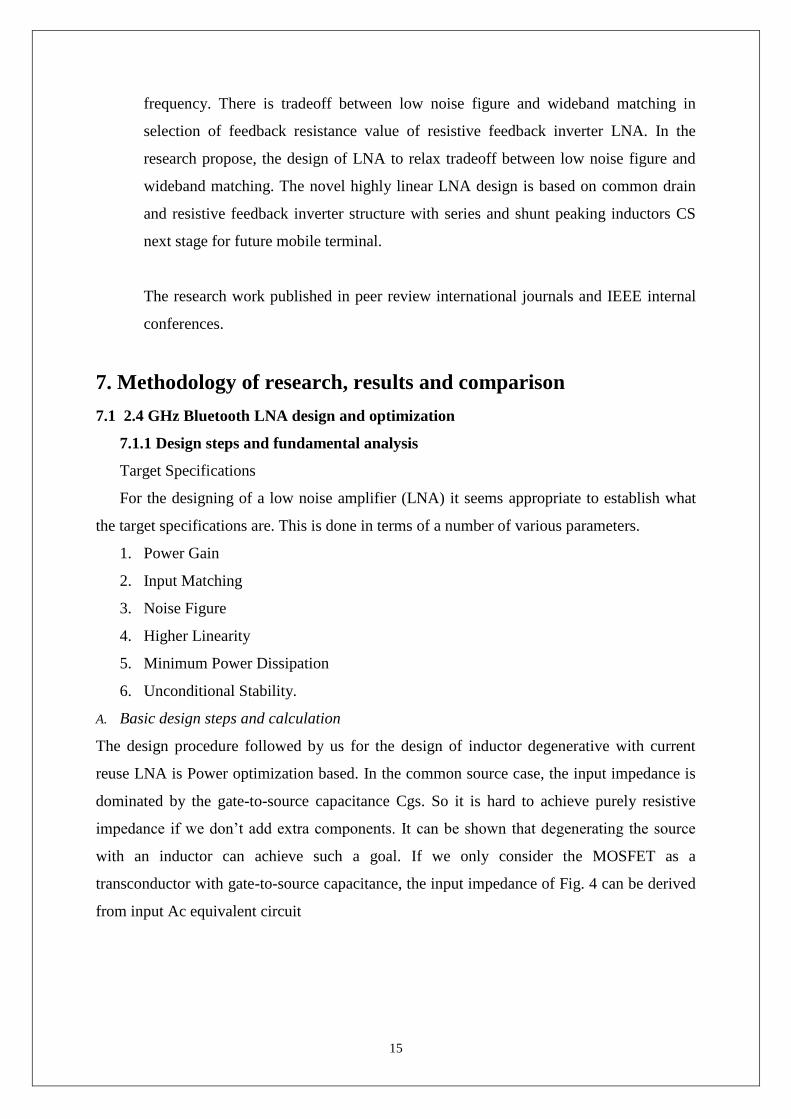
Figure 5 Inductive degenerate common source AC equivalent circuit.
Apply KCL at input loop
( ) (10)
( )
(11)
Real(Zin) =
and Imaginary(Zin) = ( )
For input match with real
50ohm Real(Zin)=50Ω =
Input matching frequency can be find by Imaginary(Zin)=0
( )
√ ( ) (12)
Inductor degerative topology produce resistive effect for to matching input source resistor
without connecting physical resistors so it has low thermal noise.
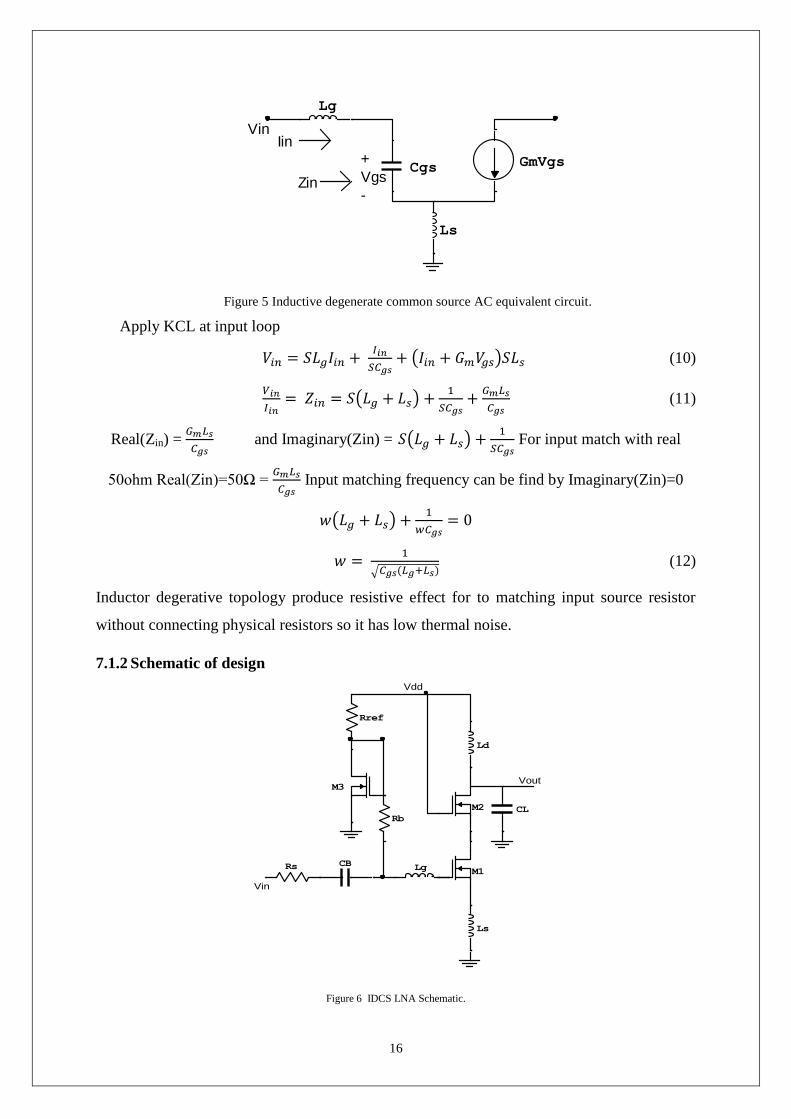
7.1.2 Schematic of design
Figure 6 IDCS LNA Schematic.
Lg
Ls
Vin
ZinCgs GmVgs+
Vgs
-
Iin
M1Lg
Ls
Rs
Vdd
Vin
Vout
Ld
CLM2
M3
CB
Rb
Rref
17
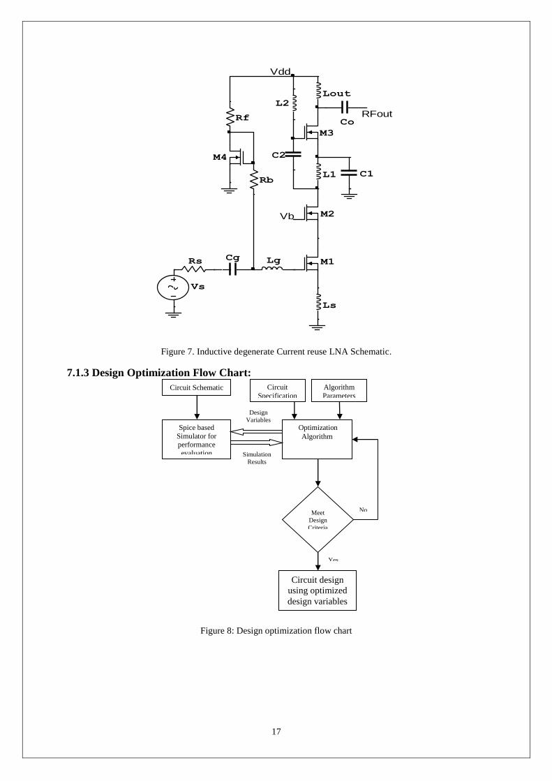
Figure 7. Inductive degenerate Current reuse LNA Schematic.
7.1.3 Design Optimization Flow Chart:
Figure 8: Design optimization flow chart
M1
M2
M3
M4
Lg
Ls
L1
Lg3
Lout
L2
Rf
Rb
C2
C1
Cg
Co
Rs
Vs
Vdd
RFout
Vb
Circuit Schematic Circuit
Specification
Algorithm
Parameters
Spice based
Simulator for performance
evaluation
Optimization
Algorithm
Design
Variables
Simulation
Results
Meet
Design
Criteria
No
Yes
Circuit design
using optimized
design variables
18
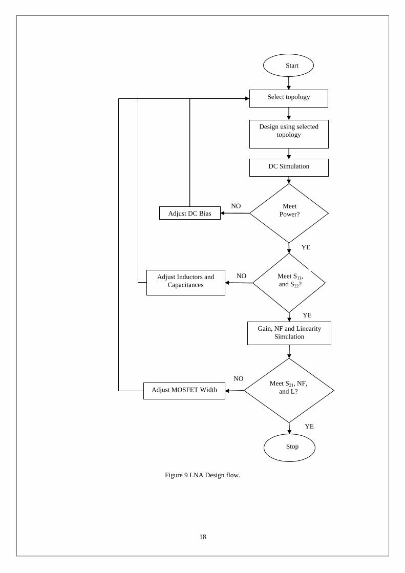
Figure 9 LNA Design flow.
Select topology
DC Simulation
Design using selected
topology
Meet
Power?
Meet S11,
and S22?
Gain, NF and Linearity
Simulation
Meet S21, NF,
and L?
Adjust DC Bias
Adjust Inductors and
Capacitances
Adjust MOSFET Width
Start
Stop
NO
NO
YE
S
YE
S
YE
S
NO
19
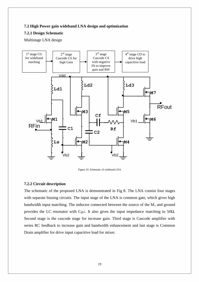
7.2 High Power gain wideband LNA design and optimization
7.2.1 Design Schematic
Multistage LNA design
7.2.1 Schematic of design
8
Figure 10. Schematic of wideband LNA
7.2.2 Circuit description
The schematic of the proposed LNA is demonstrated in Fig 8. The LNA consist four stages
with separate biasing circuits. The input stage of the LNA is common gate, which gives high
bandwidth input matching. The inductor connected between the source of the M1 and ground
provides the LC resonator with Cgs1. It also gives the input impedance matching to 50Ω.
Second stage is the cascode stage for increase gain. Third stage is Cascode amplifier with
series RC feedback to increase gain and bandwidth enhancement and last stage is Common
Drain amplifier for drive input capacitive load for mixer.
M1
M2
M3
M4
M5
M6
M7
Ls
Ld1
C2
Ld2 Ld3
C1RFin
RFout
Cf
Rf
Vb1
Vb2 Vb2
Vb1
Vdd
1st stage CG
for wideband
maching
2nd
stage
Cascode CS for
high Gain
3rd
stage
Cascode CS
with negative
f/b to improve
gain and BW
4th
stage CD to
drive high
capacitive load

20
In proposed LNA width of M1 is chosen to get the better transconductance with the source
inductor. The large value capacitor is between the M1 gate and ground ensures better AC
grounding. It is also bypasses the biasing circuit noise.
Width of M2 selection is tricky task, because value of inductor L2 restricted by the RFIC. L2
must be chosen as it will resonate with around the center frequency of interested
band. With the help of iteration the L1 value is chosen for the best noise performance. The
chosen value of Ls is much greater than value of L1. Here the two LC tank circuit formed,
one is L1 with Cgs2 + Cgd1 and another is Ls with Cgs1. These both circuits resonate around the
center frequency of the interested band.
Miller effect creates problem in the selection of the peaking frequency, to reduce miller effect
the cascode transistor added for the common source stage which cause increases the higher
frequency cutoff. Cascode stage also provides contribution to improve the gain and the
reverse isolation, without consuming more power.
First stage common gate
Figure 11. Common Gate input stage
AC equivalent circuit
Figure 12. CG AC equivalent circuit
The input impedance is calculated by
( )
( )
( )
(13)
M1
VgLs
Ld1
Rs
Vs Zin2
Ls
Rs
Vs Cgs Cgd Ld
Gm1Vgs
Ro
Zin2-
Vgs
+
21
( )
(14)
where
( )
and ( )
Assume that Zs(w) and Zo(w) are both have high Q inductor and capacitors and can represent
only imaginary part Zs(w)=jXs(w) and Zo(w)=jXo(w) And Zin can be represent as below
(
( )) (
( )) (15)
Gm1 sholud be set slightly greater than 20ms for better matching due to effect of output
resistor(Ro)
For good input matching over the wideband Ls and Cgs should be selected such that they
resonate at the center frequency leaving only 50Ω real impedance.
7.2.3 Noise analysis and optimization
As per friss formula first stage noise figure contribute major in overall noise figure of the
multistage amplifier. Here we have derive noise figure of first common gate stage.
(16)
Where
, (
) and
Using above values NF1 can be simplified as
( )
( )
(17)
From the equation shows first stage NF1 inversely proposal to transconductance (Gm) of M1 ,
input and output impedance and directly proposal to Cgs1. So, to decrease NF1 two approach
can be use.
1) Value of Ls and Cgs1 select such that it resonant at center of selected band.
2) We can increase Gm1 to reduce NF1 but input impendence degrade. Here is input
impedance and NF tradeoff. Reducing Cgs1 by reducing W of M1 will result in a lower noise
figure. On the other hand, scaling down the width of means more current is consumed to
maintain the same tranconductance. The W1 should be chose such that will improve noise
performance at given power budget.
The output impendence of the source follower is calculated as
( ) ( )
(18)
( ) ( )
(19)
22
Where and are drain to source resistor of M6 and M7 respectively the value these
resistors are very large compare to other term so it can be neglected.
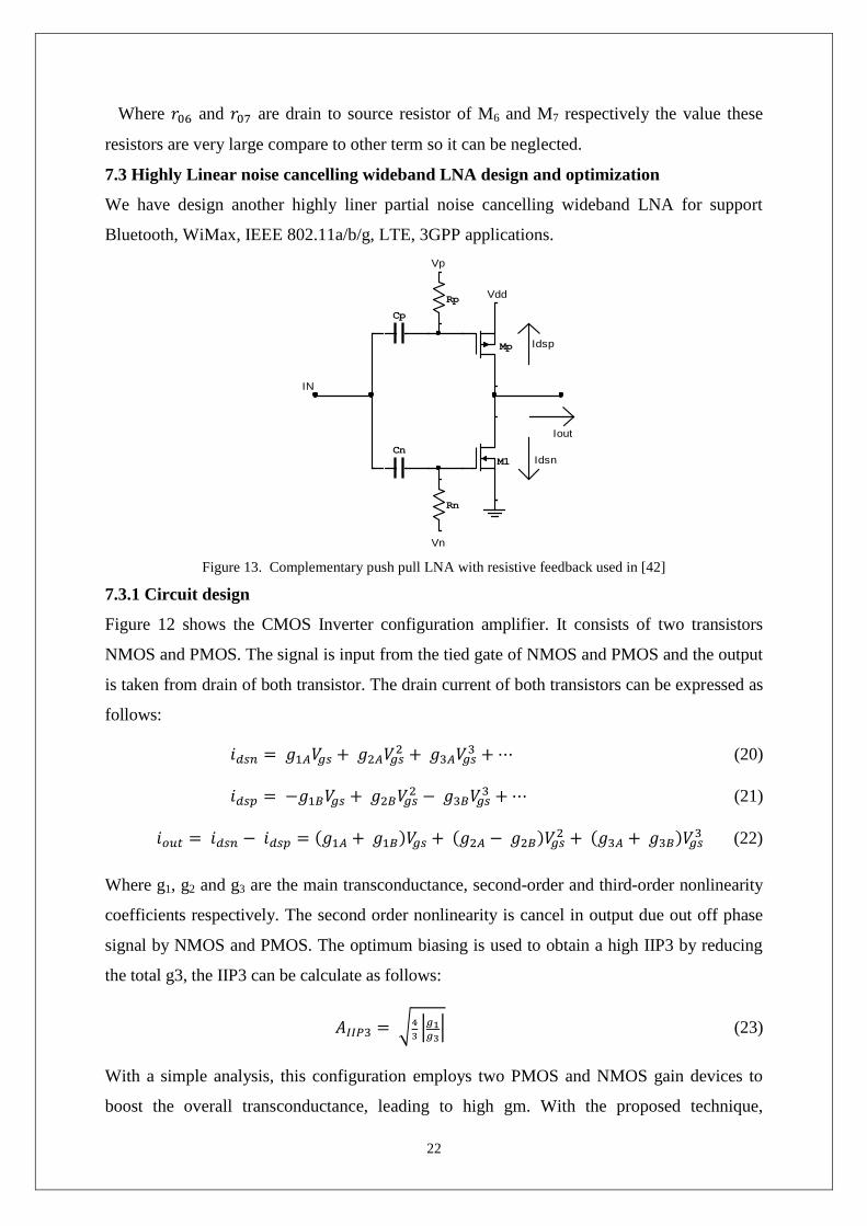
7.3 Highly Linear noise cancelling wideband LNA design and optimization
We have design another highly liner partial noise cancelling wideband LNA for support
Bluetooth, WiMax, IEEE 802.11a/b/g, LTE, 3GPP applications.
Figure 13. Complementary push pull LNA with resistive feedback used in [42]
7.3.1 Circuit design
Figure 12 shows the CMOS Inverter configuration amplifier. It consists of two transistors
NMOS and PMOS. The signal is input from the tied gate of NMOS and PMOS and the output
is taken from drain of both transistor. The drain current of both transistors can be expressed as
follows:
(20)
(21)
( ) ( ) ( )
(22)
Where g1, g2 and g3 are the main transconductance, second-order and third-order nonlinearity
coefficients respectively. The second order nonlinearity is cancel in output due out off phase
signal by NMOS and PMOS. The optimum biasing is used to obtain a high IIP3 by reducing
the total g3, the IIP3 can be calculate as follows:
√
|
| (23)
With a simple analysis, this configuration employs two PMOS and NMOS gain devices to
boost the overall transconductance, leading to high gm. With the proposed technique,
Rp
Rn
Vp
Vdd
Vn
Cp
Cn
IN
Idsp
Idsn
Iout
Mp
M1
23
reducing g3 and increasing g1 leads to highly linear and high gain performance over a wide
range of frequencies.
Noise analysis
In [42] CMOS inverter the value of the feedback resistance plays an important role in
deciding the amount of noise added to the input. There is tread off between noise figure and
wideband input matching: higher value of feedback resistor decrease NF but it not provide
wider band input matching and vice versa. [42]. This tread off can be avoid by using common
drain (CD) active feedback. Trough CD feedback we can add one more degree of freedom to
set NF and input matching for wideband. Using CD feedback cancel some amount of noise
by adding out off phase noise signals.
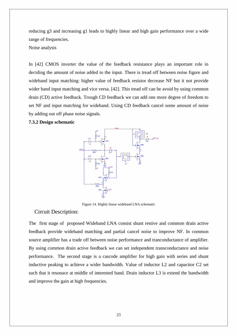
7.3.2 Design schematic
Figure 14. Highly linear wideband LNA schematic
Circuit Description:
The first stage of proposed Wideband LNA consist shunt restive and common drain active
feedback provide wideband matching and partial cancel noise to improve NF. In common
source amplifier has a trade off between noise performance and tranconductance of amplifier.
By using common drain active feedback we can set independent transconductance and noise
performance. The second stage is a cascode amplifier for high gain with series and shunt
inductive peaking to achieve a wider bandwidth. Value of inductor L2 and capacitor C2 set
such that it resonace at middle of interested band. Drain inductor L3 is extend the bandwidth
and improve the gain at high frequencies.
24
7.4 High Power Gain UWB LNA
7.4.1 Introduction
Federal Communications Commission (FCC) approved ultra wideband (UWB) technology
frequency 3.1-10.6 GHz band for commercial use in year 2002 with restriction to transmit
information using low power. Due to extremely wide bandwidth open new frontier for
wireless communication users. UWB have large transmission channel capacity and less multi
path fading due to wide bandwidth. Wireless communication in UWB used in high data rate
wireless communication, penetration imaging and high accuracy locating applications.
Despite all the favourable features of the UWB systems, serious challenges still exist for the
realization of UWB receiver front-end circuits, especially for the UWB low-noise amplifier
(LNA). Due to FCC’s stringent power-emission limitation at the transmitter and the
additional transmission path loss, the received UWB signal exhibits very low power-spectral
density (PSD) at the receiver antenna, resulting in a received signal power that is typically
three orders of magnitude smaller than that of the narrow-band transmission systems [12].
Therefore, a UWB LNA is required to provide sufficient gain over the entire 7500-MHz
bandwidth, a wide-band 50- input matching and, more importantly, a low noise figure to
enhance the sensitivity of the UWB receiver and high first stage power gain.
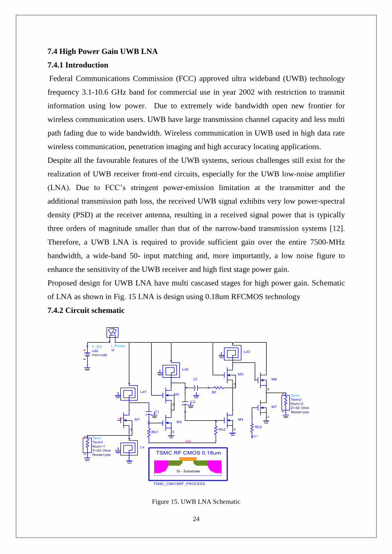
Proposed design for UWB LNA have multi cascased stages for high power gain. Schematic
of LNA as shown in Fig. 15 LNA is design using 0.18um RFCMOS technology
7.4.2 Circuit schematic
Figure 15. UWB LNA Schematic
25
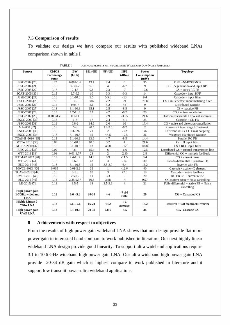
7.5 Comparison of results
To validate our design we have compare our results with published wideband LNAs
comparison shown in table I.
TABLE I. COMPARE RESULTS WITH PUBLISHED WIDEBAND LOW NOISE AMPLIFIER
Source CMOS
Technology
(um)
BW
(GHz)
S21 (dB) NF (dB) IIP3
(dBm)
Power
Consumption
(mW)
Topology
JSSC-2004 [20] 0.25 0.002-1.6 13.7 2.4 0 35 R FB +NMOS/PMOS
JSSC-2004 [21] 0.18 2.3-9.2 9.3 4 -6.7 9 CS + degeneration and input BPF
JSSC-2005 [22] 0.18 2-4.6 9.8 2.3 -7 12.6 CS + series RC FB
ICAT-2005 [23] 0.18 2.7-9.3 10 3.3 -0.3 14 Cascode + input HPF
JSSE-2006 [24] 0.18 3.1-10.6 9.5 5-5.6 -13 9.4 Cascode + input filter
JSSCC-2006 [25] 0.18 3-5 <16 2.2 -9 7.68 CS + miller effect input matching filter
JSSC-2006 [26] 0.18 0.04-7 8.6 4.2 +3 9 Distributed cascode
JSSC-2007 [27] 0.13 3.1-10.6 15.1 2.5 -8.5 9 CS + reactive FB
JSSC-2007 [28] 0.18 1.2-11.9 9.7 4.7 -6.2 20 CG + noise cancellation
JSSC-2007 [29] 0.18 SiGe 0.1-11 8 2.9 -3.55 21.6 Distributed cascode + BW enhancement
ISSCC-2007 [30] 0.13 1-7 17 2.4 -4.1 25 Cascode + CD FB
JSSC-2008 [31] 0.13 0.8-2 14.5 2.6 16 17.4 CG + noise and distortion cancellation
MJ-2008 [32] 0.18 5-6 20.5 1.8-2.6 -6.2 2 Cascode + inter stage LC network
ISSCC-2009 [33] 0.18 0.3-0.92 21 2 -3.2 3.6 Differential CG + C Cross coupling
ISSCC-2009 [34] 0.13 3.1-10.6 15 <4.5 -12.5 26 Weighted distributed cascode
TCAS-II -2010 [35] 0.18 3.1-10.6 13.9 4.7 -8.5 14.4 Parallel RC FB
MTT-s 2010 [36] 0.09 3.1-10.6 10.5 3.2 4 21.6 Cs + Π input filter
MTT-S 2010 [37] 0.18 31.-10.6 13 4.68 -12 10.34 CS + RLC input filter
RFIC 2010 [38] 0.09 21 15.4 6 -6.6 12.5 Distributed CS + tapered transmission line
MTT-2011 [39] 0.09 0.01-1.77 23 2 -2.85 2.8 Differential CG + multiple feedback
IET MAP 2012 [40] 0.18 2.4-11.2 14.8 3.9 -11.5 3.4 CG + current reuse
MTT-2012 [41] 0.13 0.6-3 42 3 -14 30 Pseudo differential + resistive FB
IJEC-2012 [42] 0.18 3.1-10.6 15 3.5-3.9 6.4 16.2 Inverter with FB
MWCL-2012 [43] 0.065 0.01-2.8 32 1 -13.6 40 Cascode + active –C element
TCAS-II-2013 [44] 0.18 0-1.3 10 3 +7.5 18 Cascode + active feedback
IJMST-2013 [45] 0.18 2.5-16 11 3.3 - 20 RC FB CS + current reuse
IJEC-2015 [46] 0.13 2.35-9.37 10.3 3.68 -4 9.97 CG current resue + noise cancelling
MJ-2015[47] 0.13 3.5-5 14 3.5-3.9 4 21 Fully differential + active FB + Noise cancelling
High power gain
1-7GHz wideband
LNA
0.18 0.6 - 5.6 20-34 4-6 -7 @3
GHz 26 CG + Cascaded CS
Highly Linear 2-
7Ghz LNA 0.18 0.6 – 5.6 16-21 <3.2 + 4
average 13.2 Resistive + CD feedback Inverter
High power gain
UWB LNA
0.18 3.1-10.6 20-30 2.8-6 -5.5 34 CG+Cascode CS
8 Achievements with respect to objectives
From the results of high power gain wideband LNA shows that our design provide flat more
power gain in interested band compare to work published in literature. Our next highly linear
wideband LNA design provide good linearity. To support ultra wideband applications require
3.1 to 10.6 GHz wideband high power gain LNA. Our ultra wideband high power gain LNA
provide 20-34 dB gain which is highest compare to work published in literature and it
support low transmit power ultra wideband applications.
26
9 Publications
We have published our work in international journal and IEEE internal conferences.
1) Hasmukh P Koringa, Dr. Vipul A Shah and Prof. Durga Misra ―Estimation and
Optimization of Power dissipation in CMOS VLSI circuit design: A Review Paper” in
IJETEE Journal march-2013 issue ISSN No. 2320-9569 Impact Factor 3.84.
2) Hasmukh P Koringa, Bhusan D Joshi and Dr. Vipul A Shah “High Power Gain Low
Noise Amplifier Design for Next Generation 1-7GHz Wideband RF Frontend RFIC
using 0.18µm CMOS” in IEEE 19th International Symposium on VLSI Design and
Test (VDAT-2015) organized by VLSI Society of India Collaboration with IEEE
Computer Society & TTTC at Nirma University Ahmedabad during june 26-29, 2015
publication available in IEEE Explore Digital Library with DOI
10.1109/ISVDAT.2015.7208105.
3) Hasmukh P Koringa and Dr. Vipul A Shah “Design and Optimization of Narrow Band
Low Noise Amplifier using 0.18µm CMOS” in IEEE international conference of
communication and networking 2015 organized by ITM University collaboration with
IEEE at ITM University, Gwalior during 19th
to 21st November 2015. Publication
available on IEEE Explore Digital Library with DOI 10.1109/ICCN.2015.21 page No.
100 to 106.
4) Hasmukh P Koringa and Dr. Vipul A Shah “Wideband Low Noise Amplifier for Next
Generation Wireless RF Frontend: A Review Paper” in IJAREST International journal
volume 3, issue 1, January 2016 page no. 116-125. e-ISSN: 2393-9877, p-ISSN:
2394-2444 Impact factor 2.125.
5) Hasmukh P Koringa, Dr. Vipul A Shah and Dr. Mihir V Shah “Highly Linear Active
feedback noise cancelling Wideband Low Noise Amplifier for Next Generation RF
Frontend using 0.18um CMOS” in IJAREST International journal volume 3, issue 1,
January 2016 page no. 148-155. e-ISSN: 2393-9877, p-ISSN: 2394-2444 Impact
factor 2.125.
10 References
[1] Abidi, ―The path to the software-defined radio receiver‖, IEEE J. Solid State Circuits 42 (5) (2007).
[2] J. Mitiola,‖The software radio architecture‖, IEEE Commun. Mag. 33 (5) (1995) 26–38
[3] T. H. Lee, The Design of CMOS Radio-Frequency Integrated Circuits, 2nded., Cambridge University Press, Cambridge, U. K, 1998.
[4] C. Toumazou, G. S. Moschytz, B. Gilbert, Trade-offs in Analog Circuit Design: The Designer's Companion,Part1,Springer,2004.
[5] H. Hashemi, A. Hajimiri, ―Concurrent multiband low-noise amplifiers theory,design and applications‖, IEEE Trans. Microwave Theory Tech. 50(1) (2002)288–301.
[6] G. Sapone, G. Palmisano, ―A 3–10GHz low-power CMOS low-noise amplifier for ultra-wideband communication‖, IEEE Trans. Microwave Theory Tech. 59 (3) (2011).
[7] R. Roovers, D. M. W. Leenaerts, J. Bergervoet, K. S. Harish, R. C. H. Beek, G. Weide, etal., ―An interference robust receiver for ultra-wideband radio in SiGe BiCMOS technology‖, IEEE J. Solid-State Circuits 40 (12) (2005) 2563–2572.
[8] M. Brandolini, P. Rossi, D. Manstretta, F. Svelto, ―Toward multi-standard mobile terminals—fully integrated receivers requirements and architectures‖, IEEE Tran. Microw. Theoryand Tech. 53 (3) (2005) 1026–1038.
27
[9] R. Ludwig and P Bretchko, RF Circuit Design, 2000, Prentice Hall.
[10] S. Andersson, C. Svenson, and O. Drugge, ―Wideband LNA for a Multistandard Wireless Receiver in 0.18µm CMOS,‖ Proceedings of the European Solid-State Circuits, September 2003, pp 655–658.
[11] C.-W Kim, M.-S. Jung, S.-G. Lee, ―Ultra-wideband CMOS low noise amplifier‖, Electronics Letters, vol. 41,no. 7,31 March 2005,pp. 384 – 385
[12] S. Vishwakarma, J. Sungyong; J. Youngjoong; ―Ultra Wideband CMOS Low Noise Amplifier With Active Input Matching‖, International Workshop on Ultra Wideband Systems, 2004. Joint with Conference on Ultra wideband Systems and Technologies. Joint UWBST & IWUWBS, 18-21 May 2004, pp. 415 – 419.
[13] A. Bevilacqua, A. Niknejad, ―An Ultra-Wideband CMOS LNA for 3.1 to 10.6 GHz Wireless Receivers‖, Digest of Technical papers of International Solid-State Circuits Conference, February 2004, pp. 382-383.
[14] F. Bruccoleri, E.A.M. Klumperink, B. Nauta, ―Wide-band CMOS low-noise amplifier exploiting thermal noise canceling‖, IEEE Journal of Solid-State Circuits, vol. 39, no. 2,Feb. 2004 pp. 275 - 282.
[15] F. Bruccoleri, E.A.M. Klumperink, B. Nauta, ―Noise cancelling in wideband CMOS LNAs‖, Digest of Technical Papers. ISSCC. 2002 IEEE International Solid-State Circuits Conference,vol.1, 3-7 Feb. 2002, pp. 406 – 407.
[16] D. M. Pozar, Microwave Engineering, 2nd Edition, 1998, John Willey & Sons.
[17] H.-T. Ahn, D.J. Allstot, ―0.5-8.5 GHz fully differential CMOS distributed amplifier‖, IEEE Journal of Solid-State Circuits, vol. 37, no. 8, Aug. 2002, pp. 985 – 993.
[18] B.M. Ballweber, R. Gupta and D.J. Allstot, ―A Fully Integrated 0.5 – 5.5 GHz CMOS Distributed Amplifier‖, IEEE Journal of Solid-State, vol. 35, Feb. 2000, pp. 231-239.
[19] R.-C. Liu, K.-L. Deng and H. Wang, ―A 0.6-22GHz Broadband CMOS Distributed Amplifier‖, Dig. of Technical papers in RFIC Symp., 2003, pp. 103-106.
[20] F.Bruccoleri, E. A. M. Klumperink, B. Nauta, ―Wide-band CMOS low-noise amplifier exploiting thermal noise canceling‖, IEEE J. Solid-State Circuits39 (2) (2004).
[21] A. Bevilacqua, A. Niknejad, ―An ultra-wideband CMOS LNA for 3.1 to 10.6GHz wireless receivers‖, IEEE J.Solid-State Circuits 39 (12) (2004) 2259–2268.
[22] C. W. Kim, M. S. Kang, P. T. Anh, H. T. Kim, S. G. Lee, ―An ultra wideband CMOS low noise amplifier for 3–5-GHz UWB system‖, IEEE J. Solid-State Circuits 40 (2) (2005)544–547.
[23] M. S. Jung, C. W. Kim, P. T. Anh, H. T. Kim, S. G. Lee, ―A 2.7–9.3 GHz CMOS wideband amplifier combined with high pass filter for UWB system‖, in Proceedings of 7th International Conference on Advanced Communication Technology (ICACT2005), February, 2005.
[24] H. L. Kao, K. C. Chang, ―Very low power CMOS LNA for UWB wireless receivers using current reused topology‖, J. Solid State Electron. no. 52 (2008) 86–90.
[25] H.-Jin Lee, D. S. Ha, Sang S. Choi, ―A 3–5 GHz CMOS UWB LNA with input matching using miller effect‖, IEEE International Solid-State Circuits Conference, 2006.
[26] F. Zhang, P. R. Kinget, ―Low power programmable gain CMOS distributed LNA‖, IEEE J. Solid-State Circuits 41 (6) (2006).
[27] M. T. Reiha, J. R. Long, ―A 1.2V reactive feedback 3.1-10.6GHz low-noise amplifier in 0.13 μm CMOS‖, IEEE J. Solid State Circuits 42 (5) (2007) 1023–1033.
[28] C. Liao, S. Liu, ―A broadband noise-canceling CMOS LNA for 3.1–10.6-GHz UWB receivers‖, IEEE J. Solid State Circuits 42 (2) (2007).
[29] P. Heydari, ―Design and analysis of a performance optimized CMOS UWB distributed LNA‖, IEEE J. Solid State Circuits 42 (9) (2007).
[30] R. Ramzan, S. Andersson, J. Dabrowskiand C. Svensson, ―A 1.4V 25mW inductorless wideband LNA in 0.13 um CMOS‖, IEEE international Solid-State Circuits Conference, 2007,pp.424–425.
[31] W. Chen, G. Liu, B. Zdravko, A. Niknejad, ―A highly linear broadband CMOS LNA Employing Noise and Distortion Cancellation‖, IEEE J. Solid-State Circuits 43 (5) (2008).
[32] S. Toofan, A. R. Rahmati, A. Abrishamifar, G. Roientan Lahiji, ―Low power and high gain current reuse LNA with modified input matching and inter-stage inductors‖, Microelectron. J. 39 (no.12) (2008) 1534–1537.
[33] S. Woo, W. Kim, C. Lee, K. Lim, J. Laskar, ―A 3.6mW Differential common gate CMOS LNA with positive negative feedback‖, IEEE International Solid-State Circuits Conference, 2009, pp.218–220.
[34] Y. J. Wangand A. Hajimiri, ―A compact low-noise weighted distributed amplifier in CMOS‖, in Proceedings of the IEEE International Solid State Circuits Conference, 2009, pp.220–222.
[35] K. C. He, M. T. Li, C. M Li, J. H. Tarng, ―Parallel RC feedback low noise amplifier for UWB applications‖, IEEE Trans. Circuits and Sys.—II: Express Briefs 57(8) (2010).
[36] H. K. Chen, Y. S. Lin, S. S. Lu, ―Analysis and design of a 1.6–28-GHz compact wideband LNA in 90-nm CMOS using a π-match input network‖, IEEE Trans. Microwave Theory Tech. 58 (8) (2010).
[37] Y. Sheng Lin, C. Zhi Chen, H. Yu Yang, C. Chen, J. H. Lee, G. W. Huang, S. S. Lu, ―Analysis and design of a CMOS UWB LNA with dual RLC branch wideband input matching network‖, IEEE Trans. Microwave Theory Tech. 58 (2) (2010).
[38] B. Machiels, P. Reynaert, M. Steyaert, ―Power efficient distributed low noise amplifier in 90nm CMOS‖, in Proceedings of the IEEE Proceedings of Radio Frequency Integrated Circuits Symposium,2010,pp.131–134.
[39] E Ahmed Sobhy, Ahmed A Helmy, S Hoyos, K Entesari and E Sanchez-Sinencio, ―A 2.8mW Sub 2dB Noise Figure Inductorless Wideband CMOS LNA Employing Multiple Feedback‖, in IEEE Trans. Of Microwave Theory and Techniques, Vol. 59 No. 12 December 2011 pp 3154-3161.
[40] J. Y. lee, H. K. Park, H. J. Chang and T. Y. Yun, ―Low Power UWB LNA with common gate and current reuse techniques‖, IET Microw, Antennas Propag., 2012, vol. 6, Iss. 7, pp. 793-799.
[41] X., Wang, J. Sturm, N. yan, X. Tan, and H. Min, ―0.6-3GHz Wideband Receiver RF Front-End With a Feedforward Noise and Distortion Cancellation Resistive-Feedback LNA‖, IEEE Trans. On Microwave Theory and Techniques, vol. 60 no. 2 February 2012 pp. 387-392.
[42] A. I. A. Galal, R. Pokharel, H. Kanaya and K. Yoshida, ―High Linearity technique for ultra wideband low noise amplifier in 0.18um CMOS technology‖, International Journal of Electronics and Communication (AEU) , Elsevier, 66 (2012) 12-17.
28
[43] L. Belostotski, A. Madanayake and L. T. Bruton, ―Wideband LNA with an Active –C Element‖, IEEE Microwave and Wireless Components Letters, vol. 22, no.. 10, October 2012 pp. 524-526.
[44] Donggu Im, ―A +9dBm output P1dB Active Feedback CMOS Wideband LA for SAW Less Receivers‖, IEEE Transaction on Circuits and Systems-II Express briefs, vol. 60, no. 7, july 2013, pp. 377-381.
[45] K. Yousef, H. Jia, R. Pokharel, A. Allam, M. Ragab, H. Kanaya and k. Yoshida, ―CMOS Ultra-Wideband Low Noise Amplifier Design‖, Internatonal Journal of Microwave Science and Technology, volume 2013.
[46] S. Arshad, R. Ramzan, K. Khurram Muhammad and Q. ul Wahab, ―A sub-10mW , noise cancelling, wideband LNA for UWB applications‖, International Journal of Electronics and Communications (AEU) Elsevier, (69) (2015) pp. 109-118.
[47] A. Zoaei, and A. amirabadi, ―A 130nm wideband fully differential linear low noise amplifier‖, Elsevier Microelectronics Journal, (46) (2015), 825-833.
[48] Reza Molavi, ― On the Design of Eideband CMOS Low Noise Amplifiers‖, Master Thesis of The University of British Columbia, September 2005.
[49] S. Arshad, F. Zafar, R. Ramzan and Q. Wahab, ―Wideband and multiband CMOS LNA As: State of the art and future prospects‖,
Elsevier Microelectronics Journal, April 2013. [50] L.E. Larson ,Integrated circuit technology options for RFICs—present status and future directions, IEEE J. Solid State Circuits 33 (3)
(1998). [51] C. Svensson, J. J. Wikner, Power consumption of analog circuits: a tutorial, Analog Integrated Circuits and Signal Processing 65
(2010) 171–184.
[52] B. Razavi,Designofa60GHzRFfrontend,IEEE.J.SolidStateCircuits41(1) (2006)17–21.
[53] V. Aparin, P. Gazzerro, J. Zhou, B. Sun, S. Szabo, E. Zeisel, et al., A highly- integrated tri-band/quad-mode SiGe BiCMOS RF-to-baseband receiver for wireless CDMA/ WBCDMA/ AMPS applications with gps capability, IEEE International Solid-State Circuits Conference Digest of Technical Papers, 2002.
[54] O. E. Erdoganetal., A single-chip quad-band GSM/GPRS transceiver in 0.18 mm standard CMOS, IEEE International Solid-State Circuits Conference Digest of Technical Papers, 2005.
[55] B. G. Perumana, J. H. C. Zhan, S. S. Taylor, B. R. Carlton, J. Laskar, Resistive- feedback CMOS low-noise amplifiers for multiband applications, IEEE Trans. Microwave Theory Tech. vol. 56 (5) (2008) 1218–1224.
[56] A. Kruth, M. Simon, K. Dufrene, R. Weigel, Z. Boos, S. Heinen, A multimode receiver front-end for software defined radio, in: Proceedings of 9th European Conferenceon Wireless Technology, September 2006, pp. 19–22.
[57] S. Wu, B. Razavi, A 900MHz/1.8GHz CMOS receiver for dual-band applications, IEEE J. Solid-State Circuits 33 (12) (1998) 2178–2185.
[58] M. Zargari, etal., A single-chip dual-band tri-mode CMOS transceiver for IEEE 802.11a/b/gWLAN, IEEE J. Solid-State Circuits 39 (12) (2004) 2239–2249.
[59] P. Zang, B. Razavi, A single-chip dual-band direct conversion IEEE 802.11a/b/g WLAN transceiver in 0.18 mm CMOS, IEEE J. Solid-State Circuits 40 (9) (2005) 1932–1939.
[60] C. P. Moreira, E. Kerheve, P. Jarry, D. Belot, A concurrent fully-integrated LNA for WLAN IEEE 802.11b/g/a applications, in: Proceedings of 36th European Microwave Conference, September 2006, pp.1552–155.
[61] A. Liscidini, M. Brandolini, D. Sanzogni, R. Castello, A0.13 μm CMOS frontend for DCS1800/UMTS/802.11b-g with multi band positive feedback low noise amplifier, IEEE J. Solid-State Circuits 41 (4) (2006) 981–989.
[62] L. H Lu, H. H. Hsieh, Y. S. Wang, A compact 2.4/5.2-GHz CMOS dual-band low noise amplifier, IEEE Microwave Wireless Components Lett. 15 (10) (2005). [49]M. Shouxian, M. Jianguo, Y. K. Seng, D. M. Anh, An integrated SiGe dual-band low noise amplifier for bluetooth, Hiper LAN and wireless LAN applications, in: Proceedings of 33rd European Microwave Conference, 2003, pp.309–312.
[63] K. L. Fong, Dual-band high-linearity variable-gain low-noise amplifiers for wireless applications, IEEE International Solid-State Circuits Conference Digest, February 1999, pp. 224–225.
[64] J. Ryynanen, K. Kivekäs, J. Jussila, A dual-band RF front-end for WCDMA and GSM applications, IEEE J. Solid-State Circuits 36 (8) (2001) 175–178.
[65] Z. Li, R. Quintal, K. O. Kenneth, A Dual-band CMOS frontend with two gain modes for wireless LAN applications, IEEE J. Solid State Circuits 39 (11) (2004) 2069–2073.
[66] S. F. Wang, Y. S. Hwang, S. C. Yan, J. J. Chen, A new CMOS wideband low noise amplifier with gain control, Integration VLSI J .44 (2011)136–143.
[67] B. M. Ballweber, Ravi Gupta, D. J. Allstot, A fully integrated 0.5–5.5-GHz CMOS distributed amplifier, IEEE Trans. Solid-State Circuits 35 (2) (2000).
[68] R. C. Liu, C. S. Lin, K. L. Deng, H. Wang, A 0.5–14GHz 10.6dB cascode distributed amplifier, Symposium on VLSI Circuits, Digest of Technical Papers, 2003, pp.139–140.
[69] P. J. Sullivan, B. J. Xavier, W. H. Ku, An integrated CMOS distributed amplifier utilizing packaging inductance, IEEE Trans. Microwave Theory Tech. 45 (10) (1997).
[70] D. Manstretta, A broadband low noise single ended input differential output amplifier with IM2 canceling, IEEE Radio Frequency Integrated Circuits Symposium, 2008, pp.79–82.
[71] Y. Lu, K. S. Yeo, A. Cabuk, J. Ma, M. A. Do, Z. Lu, A novel CMOS low noise amplifier design for 3.1–10.6GHz ultra-wide-band wireless receivers, IEEE Trans. Circuits Sys.—I: Regular Pap. 53 (8) (2006).
[72] G. H. Z. Fatin, Z. D. Koozehkanani, H. Sjoland, A technique for improveing gain and noise figure of common-gate wideband LNAs, Anal. Intgrated Circuits Signal Processing (2010) 239–244.
[73] H. Zhang, X. Fan, E. S. Sinencio, A low-power, linearized, ultra-wideband LNA design technique, IEEE J. Solid-State Circuits 44 (2) (2009).
[74] D. E. Norton, High dynamic range feedback amplifiers using lossless feedback, in: Proceedings of IEEE Symposium on Circuits and Systems,1975, pp.438–440.
[75] H. Doh, Y. Jeong, S. Jung, Y. Joo, Design of CMOS UWB low noise amplifier with cascode feedback, 47th IEEE International Midwest Symposium on Circuits and systems, 2004.
[76] Y. H. Yu, Y. S. Yang, Y. J. E. Chen, A compact wideband CMOS low noise amplifier with gain flatness enhancement, IEEE J. Solid-State Circuits 45 (3) (2010) 502–509.
29
[77] S. F. Wang, Y. S. Hwang, S. C. Yan, J. J. Chen, A new CMOS wideband low noise amplifier with gain control, Integration, the VLSI Journal 44 (2011)136–143.
[78] Z. Ru, E. A. M. Klumperink, C. E. Saavedra, BramNauta, A 300–800MHz tunable filter and linearized LNA applied in a low-noise harmonic rejection RF- sampling receiver, IEEE J. Solid-State Circuits 45 (5) (2010) 967–978.
[79] Po-Yu Chang, Shawn S. H. Hsu, A compact 0.1–14GHz ultra-wideband low- noise amplifier in 0.13-mm CMOS, IEEE Trans. Microwave Theory Tech. 58 (10) (2010).
[80] M. E. Nozahi, A. A. Helmy, E. S. Sinencio, K. Entesari, A 2–1100MHz wideband low noise amplifier with 1.43dB minimum noise figure, IEEE Radio Fre quency Integrated Circuits Symposium., pp. 119–122, 2010.
[81] M. E. Nozahi, A. A. Helmy, E. S. Sinencio, K. Entesari, An inductorless noise canceling broadband low noise amplifier with composite transistor pair in 90 nm CMOS technology, IEEE J. Solid-State Circuits 46 (5) (2011) 1111–1122.
[82] J. H. Lee, C. C. Chen, H. Y. Wang, Y. S. Lin, A 2.5-dB NF 3.1–10.6-GHz CMOS UWB LNA with small group-delay-variation, in: Proceedings of IEEE Radio Fre quency Integrated Circuits Symposium, pp.501–504, 2008.
[83] R. Gharpurey, A broad band low noise front-end amplifier for ultra wideband in 0.13 mm CMOS, IEEE J. Solid State Circuits 40 (9) (2005).
[84] J. Jung, T. Yun, J. Choi, Ultra-wideband low noise amplifier using a cascode feedback topology, Microw. Optical Tech. Lett. 48 (no.6) (2006).
[85] K. C. He, M. T. Li, C. MLi, J. H. Tarng, Parallel RC feedback low noise amplifier for UWB applications, IEEE Trans. Circuits and Sys.—II: Express Briefs 57(8) (2010).
[86] M. Vidojkovic, J. V. Tang, M. Sanduleanu, P. Baltus, A. V. Roermund, Abroad- band, inductorless LNA for multi-standard applications, in: Proceedings of IEEE European Conference on Circuit Theory and Design, 2007.
[87] M. Vidojkovic, M. Sanduleanu, J. V. Tang, P. Baltus, A. V. Roermund, A 1.2V, inductorless, broadband LNA in 90nm CMOS LPIEEE Radio Frequency Integrated Circuits Symposium., pp. 53–56, 2007.
[88] Y. Soliman, L. MacEachern, L. Roy, A CMOS ultra-wideband LNA utilizing a frequency-controlled feedback technique, in: Proceedings of IEEE International Conference on Ultra-Wideband (ICU), 2005, pp.530–535.
[89] M. T. Reiha, J. R. Long, A 1.2V reactive feedback 3.1-10.6GHz low-noise amplifier in 0.13μm CMOS, IEEE J. Solid State Circuits 42 (5) (2007) 1023–1033.
[90] K. W. Tang, M. Khanpour, P. Garcia, C. Garnier, S. P. Voinigescu, 65-nm CMOS, W-band receivers for imaging applications, in: Proceedings of IEEE Custom Integrated Circuits Conference(CICC), 2007, pp.749–752.
[91] A. C. Heiberg, T. W. Brown, T. S. Fiez, K. Mayaram, A 250mV, 352mW GPS receiver RF front-end in130nm CMOS, IEEE J. Solid-State Circuits 46 (4) (2011) 938–949.
[92] A. Nieuwoudt, T. Ragheb, H. Nejati, Y. Massoud, Numerical design optimization methodology for wideband and multi-band inductively degenerated cascode CMOS low noise amplifiers, IEEE Trans. Circuits Syst.—I Regular Pap. 56 (6) (2009).
[93] W. Zhuo, etal., A capacitor cross-coupled common gate low-noise amplifier, IEEE Trans. Circuits Syst. II, Exp. Briefs 52 (no.12) (2005) 875–879.
[94] S. Woo, W. Kim, C. Lee, K. Lim, J. Laskar, A 3.6mW Differential common gate CMOS LNA with positive negative feedback, IEEE International Solid-State Circuits Conference, 2009, pp.218–220.
[95] J. Kim, S. Hoyos, J. Martinez, Wideband common-gate CMOS LNA employing dual negative feedback with simultaneous noise, gain, and bandwidth optimization, IEEE Trans. Microwave Theory Tech. 58 (9) (2010).