Embed Size (px)
Citation preview
Audio Switching Amplifier AD1990
Rev. 0 Information furnished by Analog Devices is believed to be accurate and reliable. However, no responsibility is assumed by Analog Devices for its use, nor for any infringements of patents or other rights of third parties that may result from its use. Specifications subject to change without notice. No license is granted by implication or otherwise under any patent or patent rights of Analog Devices. Trademarks and registered trademarks are the property of their respective owners.
One Technology Way, P.O. Box 9106, Norwood, MA 02062-9106, U.S.A.Tel: 781.329.4700 www.analog.com Fax: 781.461.3113 ©2006 Analog Devices, Inc. All rights reserved.
FEATURES Integrated stereo modulator and power stage <0.002% THD + N 101 dB dynamic range (A-weighted) 2 × 5 W output power (4 Ω, <0.01% THD + N) RDS-ON < 0.3 Ω (per transistor) PSRR > 65 dB On-off-mute pop noise suppression EMI optimized modulator Short-circuit protection Overtemperature protection Low cost DMOS process
APPLICATIONS Advanced televisions Compact multimedia systems Minicomponents
GENERAL DESCRIPTION
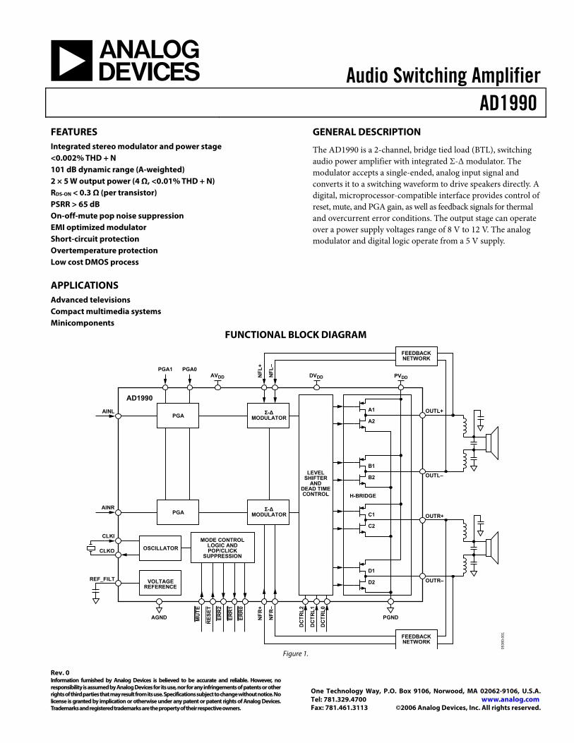
The AD1990 is a 2-channel, bridge tied load (BTL), switching audio power amplifier with integrated Σ-Δ modulator. The modulator accepts a single-ended, analog input signal and converts it to a switching waveform to drive speakers directly. A digital, microprocessor-compatible interface provides control of reset, mute, and PGA gain, as well as feedback signals for thermal and overcurrent error conditions. The output stage can operate over a power supply voltages range of 8 V to 12 V. The analog modulator and digital logic operate from a 5 V supply.
FUNCTIONAL BLOCK DIAGRAM
B2
B1
A2
A1 OUTL+
LEVELSHIFTER
ANDDEAD TIMECONTROL H-BRIDGE
PGND
OUTL–
OUTR+
DC
TRL2
DC
TRL1
DC
TRL0
OUTR–D2
D1
C2
C1
NFR
+
NFR
–
NFL
+
NFL
–
MU
TE
RES
ET
ERR
2
ERR
1
ERR
0
Σ-ΔMODULATOR
Σ-ΔMODULATOR
PGA
PGA
OSCILLATOR
VOLTAGEREFERENCE
MODE CONTROLLOGIC ANDPOP/CLICK
SUPPRESSION
AGND
CLKI
CLKO
REF_FILT
AINR
AINL
PVDDAVDD DVDDPGA1 PGA0
FEEDBACKNETWORK
FEEDBACKNETWORK
AD1990
0538
0-00
1
Figure 1.

AD1990
Rev. 0 | Page 2 of 16
TABLE OF CONTENTS Features .............................................................................................. 1
Applications....................................................................................... 1
General Description ......................................................................... 1
Functional Block Diagram .............................................................. 1
Revision History ............................................................................... 2
Specifications..................................................................................... 3
Absolute Maximum Ratings............................................................ 5
ESD Caution.................................................................................. 5
Pin Configuration and Function Descriptions............................. 6
Typical Performance Characteristics ............................................. 8
Theory of Operation ...................................................................... 11
Overview ..................................................................................... 11
Σ-Δ Modulator............................................................................ 11
MUTE and RESET ..................................................................... 11
Gain Structure............................................................................. 11
Power Stage ................................................................................. 13
Clocking....................................................................................... 13
Protection Circuits and Error Reporting ................................ 14
Application Circuits ....................................................................... 15
Outline Dimensions ....................................................................... 16
Ordering Guide .......................................................................... 16
REVISION HISTORY
4/06—Revision 0: Initial Version

AD1990
Rev. 0 | Page 3 of 16
SPECIFICATIONS Test conditions, unless otherwise specified.
Table 1. Parameter Ratings SUPPLY VOLTAGES
AVDD 5 V DVDD 5 V PVDD 12 V
AMBIENT TEMPERATURE 25°C LOAD IMPEDANCE 6 Ω CLOCK FREQUENCY 12.288 MHz PGA GAIN 0 dB MEASUREMENT BANDWIDTH 20 Hz to 20 kHz
Table 2. Parameter Min Typ Max Unit Test Conditions/Comments RDS-ON
Per High-Side Transistor 260 355 mΩ T = 25°C Per Low-Side Transistor 210 265 mΩ T = 25°C
MAXIMUM CURRENT THROUGH OUTx 5 A Peak THERMAL WARNING ACTIVE 135 °C Die temperature THERMAL SHUTDOWN ACTIVE 150 °C Die temperature RESTORE TEMPERATURE AFTER THERMAL SHUTDOWN 120 °C Die temperature
Table 3. Performance Specifications Parameter Typ Unit Test Conditions/Comments TOTAL HARMONIC DISTORTION AND NOISE (THD + N) 0.003 % PGA = 0 dB, PO = 1 W, 1 kHz 0.006 % PGA = 6 dB, PO = 1 W, 1 kHz 0.01 % PGA = 12 dB, PO = 1 W, 1 kHz 0.02 % PGA = 18 dB, PO = 1 W, 1 kHz SIGNAL-TO-NOISE RATIO (SNR) 102 dB 1 kHz, A-weighted, 0 dB referred to 1% THD + N output DYNAMIC RANGE (DNR) 102 dB 1 kHz, A-weighted, −60 dB referred to 1% THD + N output CROSSTALK (LEFT-TO-RIGHT OR RIGHT-TO-LEFT) −100 dB PGA = 0 dB, PO = 5 W, 1 kHz
Table 4. DC Specifications Parameter Typ Unit Test Conditions/Comments INPUT IMPEDANCE 20 kΩ AINL, AINR input pins OUTPUT DC OFFSET ±4 mV Independent of PGA setting

AD1990
Rev. 0 | Page 4 of 16
Table 5. Power Supplies Parameter Min Typ Max Unit Test Conditions/Comments ANALOG SUPPLY, AVDD 4.5 5.0 5.5 V DIGITAL SUPPLY, DVDD 4.5 5.0 5.5 V POWER TRANSISTOR SUPPLY, PVDD 6.5 8 to 12 15 V RESET/POWER-DOWN CURRENT RESET held low
AVDD 0.6 1 μA 5 V DVDD 7.5 11 μA 5 V PVDD 19 40 μA 12 V
QUIESCENT CURRENT Inputs grounded, nonoverlap = minimum AVDD 20 mA 5 V DVDD 5.5 mA 5 V PVDD 30 mA 12 V
OPERATING CURRENT VIN = 1 V rms, RL = 6 Ω, PO = 1 W AVDD 20 27 mA 5 V DVDD 5.5 7 mA 5 V PVDD 218 260 mA 12 V
Table 6. Digital I/O Parameter Min Typ Max Unit Test Conditions/Comments INPUT LOGIC HIGH 2.0 V INPUT LOGIC LOW 0.8 V OUTPUT LOGIC HIGH 2.4 V @ 4 mA OUTPUT LOGIC LOW 0.4 V @ 4 mA LEAKAGE CURRENT ON DIGITAL OUTPUTS 10 μA
Table 7. Digital Timing Parameter Typ Unit Test Conditions/Comments tMD 10 μs Delay after MUTE is asserted until output stops switching
tUD 34 μs Delay after MUTE is deasserted until output starts switching
MUTE
OUTx
tUDtMD
0538
0-00
2
Figure 2. Mute and Unmute Delay Timing
AD1990
Rev. 0 | Page 5 of 16
ABSOLUTE MAXIMUM RATINGS
Table 8. Parameter Rating AVDD, DVDD to AGND, DGND −0.3 V to +6.5 V PVDDx to PGNDx1 −0.3 V to +22.5 V AGND to DGND to PGNDx −0.3 V to +0.3 V AVDD, to DVDD −0.5 V to +0.5 V Operating Temperature Range –40°C to +85°C Storage Temperature Range –65°C to +150°C Maximum Junction Temperature 150°C
Thermal Resistance
θJA 19.2°C/W
θJC (at the Exposed Pad Surface) 0.9°C/W
θJB (on JEDEC Standard PCB) 9.7°C/W 1 Including any induced voltage due to inductive load.
Stresses above those listed under Absolute Maximum Ratings may cause permanent damage to the device. This is a stress rating only; functional operation of the device at these or any other conditions above those indicated in the operational section of this specification is not implied. Exposure to absolute maximum rating conditions for extended periods may affect device reliability.
ESD CAUTION ESD (electrostatic discharge) sensitive device. Electrostatic charges as high as 4000 V readily accumulate on the human body and test equipment and can discharge without detection. Although this product features proprietary ESD protection circuitry, permanent damage may occur on devices subjected to high energy electrostatic discharges. Therefore, proper ESD precautions are recommended to avoid performance degradation or loss of functionality.

AD1990
Rev. 0 | Page 6 of 16
PIN CONFIGURATION AND FUNCTION DESCRIPTIONS
PIN 1INDICATOR
17 18 19 20 21 22 23 24 25 26 27 28 29 30 31 32
ERR
2ER
R1
ERR
0D
CTR
L2D
CTR
L1D
CTR
L0D
GN
DD
VDD
DVD
DD
GN
DC
LKI
CLK
OM
UTE
RES
ETPG
A1
PGA
0
64 63 62 61 60 59 58 57 56 55 54 53 52 51 50 49
PGN
D1
NFL
+N
FL–
NC
AIN
LN
CM
OD
_FIL
TA
VDD
AG
ND
REF
_FIL
TN
CA
INR
NC
NFR
–N
FR+
PGN
D2
123456789
10111213141516
PGND1PGND1PGND1OUTL+OUTL+OUTL+PVDD1PVDD1PVDD1PVDD1OUTL–OUTL–OUTL–PGND1PGND1PGND1
NC = NO CONNECT
PGND2PGND2PGND2OUTR+OUTR+OUTR+PVDD2PVDD2PVDD2PVDD2OUTR–OUTR–OUTR–PGND2PGND2PGND2
48474645444342414039383736353433
AD1990TOP VIEW
(Not to Scale)
0538
0-00
3
Figure 3. Pin Configuration
Table 9. Pin Function Descriptions Pin No. Mnemonic In/Out Description 1, 2, 3, 64 PGND1 Negative Power Supply. Used for the A2 and B2 high power transistors. 4, 5, 6 OUTL+ O Output of Transistor Pair A1 and A2. 7, 8, 9, 10 PVDD1 Positive Power Supply. Used for the A1 and B1 high power transistors. 11, 12, 13 OUTL− O Output of Transistor Pair B1 and B2. 14, 15, 16 PGND1 Negative Power Supply. Used for the A2 and B2 high power transistors. 17 ERR2 O Active Low Thermal Shutdown Error Output.
18 ERR1 O Active Low Thermal Warning Error Output.
19 ERR0 O Active Low Overcurrent Error Output.
20 DCTRL2 I/O Nonoverlap Time Setting MSB. 21 DCTRL1 I Nonoverlap Time Setting. 22 DCTRL0 I Nonoverlap Time Setting LSB. 23, 26 DGND Negative Power Supply for Low Power Digital Circuitry. 24, 25 DVDD Positive Power Supply for Low Power Digital Circuitry. 27 CLKI I Clock Input for 256 × fS Audio Modulator Clock. 28 CLKO O Inverted Version of CLKI for Use with an External XTAL Oscillator. 29 MUTE I Active Low Mute Input.
30 RESET I Active Low Reset Input. 31 PGA1 I PGA Gain Control MSB. 32 PGA0 I PGA Gain Control LSB. 33, 34, 35 PGND2 Negative Power Supply for High Power Transistors C2 and D2. 36, 37, 38 OUTR− O Output of Transistor Pair D1 and D2. 39, 40, 41, 42 PVDD2 Positive Power Supply for High Power Transistors C1 and D1. 43, 44, 45 OUTR+ O Output of Transistor Pair C1 and C2. 46, 47, 48, 49 PGND2 Negative Power Supply for High Power Transistors C2 and D2. 50 NFR+ I Right Channel Negative Feedback—Noninverting Input. 51 NFR− I Right Channel Negative Feedback—Inverting Input.

AD1990
Rev. 0 | Page 7 of 16
Pin No. Mnemonic In/Out Description 52, 54, 59, 61 NC No Connection—Should Be Left Floating. 53 AINR I Analog Input for Right Channel. 55 REF_FILT O Filter Pin for Band Gap Reference—Should Be Bypassed to AGND. 56 AGND Negative Power Supply for Low Power Analog Circuitry. 57 AVDD Positive Power Supply for Low Power Analog Circuitry. 58 MOD_FILT O Modulator Filter Pin—Used to Set Time Constant of Modulator Order Reduction Circuit. 60 AINL O Analog Input for Left Channel. 62 NFL− I Left Channel Negative Feedback—Inverting Input. 63 NFL+ I Left Channel Negative Feedback—Noninverting Input. 64 PGND1 Negative Power Supply. Used for the A2 and B2 high power transistors.

AD1990
Rev. 0 | Page 8 of 16
FREQUENCY (kHz)
POW
ER (d
BFS
: 0dB
= P
ower
at W
hich
THD
= 1
% (5
.9W
))
TYPICAL PERFORMANCE CHARACTERISTICS
0
–1600 20
–20
–40
–60
–80
–100
–120
–140
2 4 6 8 10 12 14 16 1805
380-
004
FREQUENCY (kHz)
POW
ER (d
BFS
: 0dB
= P
ower
at W
hich
THD
= 1
% (4
.0W
))
Figure 4. 1 W Output Power into 4 Ω Load
0
–1600 20
–20
–40
–60
–80
–100
–120
–140
2 4 6 8 10 12 14 16 18
0538
0-00
5
FREQUENCY (kHz)
POW
ER (d
BFS
: 0dB
= P
ower
at W
hich
THD
= 1
% (3
.0W
))
Figure 5. 1 W Output Power into 6 Ω Load
0
–1600 20
0538
0-00
6
0
–1600 20
FREQUENCY (kHz)
POW
ER (d
BFS
: 0dB
= P
ower
at W
hich
THD
= 1
% (5
.9W
))
–20
–40
–60
–80
–100
–120
–140
2 4 6 8 10 12 14 16 18
0538
0-00
7
0
–1600 20
FREQUENCY (kHz)
POW
ER (d
BFS
: 0dB
= P
ower
at W
hich
THD
= 1
% (4
.0W
))
–20
–40
–60
–80
–100
–120
–140
2 4 6 8 10 12 14 16 18
Figure 6. 1 W Output Power into 8 Ω Load
Figure 7. −60 dBFS Output Power into 4 Ω Load
–20
–40
–60
–80
–100
–120
–140
2 4 6 8 10 12 14 16 18
0538
0-00
8
0
–1600 20
FREQUENCY (kHz)
POW
ER (d
BFS
: 0dB
= P
ower
at W
hich
THD
= 1
% (3
.0W
))
Figure 8. −60 dBFS Output Power into 6 Ω Load
–20
–40
–60
–80
–100
–120
–140
0538
0-00
9
2 4 6 8 10 12 14 16 18
Figure 9. −60 dBFS Output Power into 8 Ω Load
AD1990
Rev. 0 | Page 9 of 16
20
–140
FREQUENCY (Hz)
POW
ER (d
B, R
elat
ive
to 5
00m
W O
utpu
t Pow
er)
0
–20
–40
–60
–80
–100
–120
100 1k 10k
0538
0-01
0
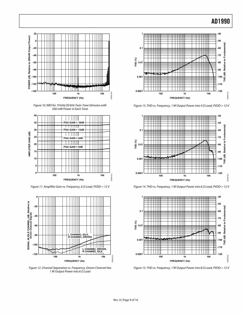
Figure 10. IMD for 19 kHz/20 kHz Twin-Tone Stimulus with 500 mW Power in Each Tone
40
0
FREQUENCY (Hz)
AM
PLIF
IER
GA
IN (d
B)
100 1k 10k
35
30
25
20
15
10
5
PGA GAIN = 18dB
PGA GAIN = 12dB
PGA GAIN = 6dB
PGA GAIN = 0dB
0538
0-01
1
Figure 11. Amplifier Gain vs. Frequency, 6 Ω Load, PVDD = 12 V
0
–120
FREQUENCY (Hz)
SIG
NA
L IN
IDLE
CH
AN
NEL
(dB
, Rel
ativ
e to
Driv
en C
hann
el S
igna
l)
100 1k 10k
–20
–40
–60
–80
–100
L CHANNEL DRIVEN,R CHANNEL IDLE
L CHANNEL IDLE,R CHANNEL DRIVEN
0538
0-01
2
Figure 12. Channel Separation vs. Frequency, Driven Channel Has 1 W Output Power into 6 Ω Load
1
0.0001
FREQUENCY (Hz)
100 1k 10k
THD
(%)
0.1
0.01
0.001
–120
THD
(dB
, Rel
ativ
e to
Fun
dam
enta
l)
–60
–40
–50
–80
–90
–70
–100
–110
0538
0-01
3
Figure 13. THD vs. Frequency, 1 W Output Power into 4 Ω Load, PVDD = 12 V
1
0.0001
FREQUENCY (Hz)
100 1k 10k
THD
(%)
0.1
0.01
0.001
–120
THD
(dB
, Rel
ativ
e to
Fun
dam
enta
l)
–60
–40
–50
–80
–90
–70
–100
–110
0538
0-01
4
Figure 14. THD vs. Frequency, 1 W Output Power into 6 Ω Load, PVDD = 12 V
1
0.0001
FREQUENCY (Hz)
100 1k 10k
THD
(%)
0.1
0.01
0.001
–120
THD
(dB
, Rel
ativ
e to
Fun
dam
enta
l)
–60
–40
–50
–80
–90
–70
–100
–110
0538
0-01
5
Figure 15. THD vs. Frequency, 1 W Output Power into 8 Ω Load, PVDD = 12 V

AD1990
Rev. 0 | Page 10 of 16
100
0.001
OUTPUT POWER (W)
0.1 1 10
THD
OR
TH
D +
N (%
)
–100
–90
–80
–70
–60
–50
–40
–30
–20
–10
THD
OR
TH
D +
N (d
B, R
elat
ive
to F
unda
men
tal)
0
10
1
0.1
0.01THD + N
THD
0538
0-01
6
Figure 16. THD and THD + N vs. Output Power, 1 kHz Sine, 4 Ω Load, PVDD = 12 V
100
0.001
OUTPUT POWER (W)
0.1 1 10
THD
OR
TH
D +
N (%
)
–100
–90
–80
–70
–60
–50
–40
–30
–20
–10
THD
OR
TH
D +
N (d
B, R
elat
ive
to F
unda
men
tal)
0
10
1
0.1
0.01THD + N
THD
0538
0-01
7
Figure 17. THD and THD + N vs. Output Power, 1 kHz Sine, 6 Ω Load, PVDD = 12 V
100
0.001
OUTPUT POWER (W)
0.1 1 10
THD
OR
TH
D +
N (%
)
–100
–90
–80
–70
–60
–50
–40
–30
–20
–10
THD
OR
TH
D +
N (d
B, R
elat
ive
to F
unda
men
tal)
0
10
1
0.1
0.01THD + N
THD
0538
0-01
8
Figure 18. THD and THD + N vs. Output Power, 1 kHz Sine, 8 Ω Load, PVDD = 12 V
10
0
PVDD VOLTAGE (V)
8.0 12.0
OU
TPU
T PO
WER
PER
CH
AN
NEL
(W) 9
8
7
6
5
4
3
2
1
8.5 9.0 9.5 10.0 10.5 11.0 11.5
THD = 10%
THD = 1%
0538
0-01
9
Figure 19. Maximum Output Power vs. PVDD, 4 Ω Load
10
0
PVDD VOLTAGE (V)
8.0 12.0
OU
TPU
T PO
WER
PER
CH
AN
NEL
(W) 9
8
7
6
5
4
3
2
1
8.5 9.0 9.5 10.0 10.5 11.0 11.5
THD = 10%
THD = 1%
0538
0-02
0
Figure 20. Maximum Output Power vs. PVDD, 6 Ω Load
10
0
PVDD VOLTAGE (V)
8.0 12.0
OU
TPU
T PO
WER
PER
CH
AN
NEL
(W) 9
8
7
6
5
4
3
2
1
8.5 9.0 9.5 10.0 10.5 11.0 11.5
THD = 10%
THD = 1%
0538
0-02
1
Figure 21. Maximum Output Power vs. PVDD, 8 Ω Load
AD1990
Rev. 0 | Page 11 of 16
THEORY OF OPERATION OVERVIEW The AD1990 is a 2-channel, high performance, switching, audio power amplifier. Each of the two Σ-Δ modulators converts a single-ended analog input into a 2-level pulse stream that controls the differential, full H-bridge, power output stage. The combination of an Σ-Δ modulator and a switching power stage provides an inherently linear and efficient means of amplifying the entire range of audio frequencies. The AD1990 also offers warning and protection circuits for overcurrent and over-temperature conditions, as well as silent turn-on and turn-off transitions.
Σ-Δ MODULATOR The AD1990 is a switching type, also known as a Class-D, audio power amplifier. This class of amplifiers maximizes efficiency by only using its power output devices in full-on or full-off states. While most Class-D amplifiers use some variation of pulse-width modulation (PWM), the AD1990 uses Σ-Δ modulation to determine the switching pattern of the output devices. This provides a number of important benefits. Σ-Δ modulators do not produce a sharp peak with many harmonics in the AM frequency band as pulse-width modulators (PWM) often do. In addition, the 1-bit quantizer produces excellent linearity across the full amplitude range.
Σ-Δ modulators require feedback to generate an error signal with respect to the input. The feedback voltages for the AD1990 modulators come from the outputs of the power devices and before the passive low-pass filters (see Figure 23). This compensates for nonlinear behavior in the power stage, such as nonoverlap time, mismatched rise and fall times, and propagation delays. It also reduces sensitivity to both dc and transient changes of the power supply voltage.
Σ-Δ modulators operate in discrete time. As with all time-quantized systems, the Nyquist frequency is equal to half of the sampling frequency and input signals above that point aliases back into the base band. The AD1990 sampling frequency (master clock) is equal to half the frequency of the input clock, approximately 6 MHz, so images only alias for input frequencies above approximately 3 MHz. This is far enough above the audio band that bandwidth and aliasing are not a problem in real applications.
The modulator has a noise shaping effect, and SNR is increased in the audio band by shifting the quantization noise upward in frequency. For a nominal input clock frequency of 12.288 MHz, the noise floor rises sharply above 20 kHz. The actual clock frequency used in an application circuit can deviate from this rate by as much as ±10%, and the corner frequency of the noise scales proportionately. The frequency at which the quantization noise dominates the output determines the amplifier’s practical bandwidth.
MUTE AND RESET
When power is applied and the RESET pin remains asserted, the AD1990 is in its lowest power consumption mode. The analog modulator is not running, and the power stage is tri-stated. On deasserting the RESET pin, the modulator begins a start-up sequence that includes initialization of the modulator, the protection circuits, and other functions.
Once the start-up sequence is complete, the amplifier is in a state in which the modulator is running, but the output stage is not driven. When MUTE is deasserted, the output is started using a soft-start sequence that avoids any audible pop or click noise in the output signal.
The output power transistors do not switch while MUTE remains asserted. Unlike the analog mute circuits found on some amplifiers that can be limited in their attenuation by the control logic or crosstalk, the mute attenuation on the AD1990 is greater than its dynamic range. The noise floor of the output signal also drops while in MUTE because the output transistors are not switching.
Power-Up Sequencing
Careful power-up is necessary when using the AD1990 to ensure correct operation and to avoid possible latch-up issues. The AD1990 should be powered up with RESET and MUTE held low until all the power supplies have stabilized. Once the supplies have stabilized, bring the AD1990 out of RESET by bringing RESET high.
Begin the soft unmute sequence by bringing MUTE high at least 1 sec after the RESET rising edge. The amplifier produces audio using a shorter start-up sequence (as shown in Table 7), but the amplifier can produce an audible pop or click noise as the output starts switching. This is because the ac coupling capacitors at the analog input have a long time constant. If MUTE is deasserted substantially less than 1 sec after deasserting RESET, then these capacitors may not have charged to a steady state. They need ample time to settle at a bias voltage of VREF, the reference voltage for the single-ended inputs, or the amplifier starts with a slight dc offset.
GAIN STRUCTURE Analog Input Levels
The AD1990 has single-ended inputs for the left and right channels. The analog input section uses an internal amplifier to bias the input signal to the reference level, VREF, which is nominally equal to AVDD/2. A dc-blocking capacitor, as shown in Figure 22, prevents this bias voltage from affecting the signal source. In combination with the nominal 20 kΩ input impedance, the value of this capacitor should be large enough to produce a flat frequency response at the lowest input frequency of interest.

AD1990
Rev. 0 | Page 12 of 16
Note that the amplifier is capable of dc-coupled operation if the circuit includes some means to account for this bias voltage.
AINL/AINR0V
+
0538
0-02
8
Figure 22. AC-Coupled Input Signal
Setting the Modulator Gain
The AD1990 modulator uses a combination of the input signal and feedback from the power output stage to calculate its two-state output pattern. The feedback input nodes are part of the internal analog circuit that operates from the AVDD (nominal 5 V) power supply. Because the voltage measured at the power outputs is nominally between 0 V and PVDD, and thus beyond the 0 V to AVDD range, a voltage divider is required to scale the feedback to an appropriate level.
Resistor voltage dividers should sense the voltage on each side of the differential output and provide these feedback signals to the modulator, as shown in Figure 23.
EXTERNAL COMPONENTS
R1 R3C C
L LRL
D2 D4
D1 D3OUTx+ OUTx–
R2 R4
PVDD PVDD
NFx+ NFx–PGND PGND
0538
0-02
9
Figure 23. H-Bridge Configuration
The resistor values should satisfy the following equation to maintain modulator stability.
635.3443
221 DDPV
RRR
RRRGain =
+=
+=
Selecting a gain that meets this criterion ensures that the modulator remains in a stable operating condition.
The ratio of the resistances sets the gain rather than the absolute values. However, the dividers provide a path from the high voltage supply to ground; therefore, the values should be large enough to produce negligible loss due to quiescent current.
The chip contains a calibration circuit to minimize voltage offsets at the speaker, which helps to minimize clicks and pops when muting or unmuting. Optimal performance is achieved for the offset calibration circuit when the feedback divider resistors sum to 6 kΩ, that is, (R1 + R2) = 6 kΩ, and (R3 + R4) = 6 kΩ.
This fixed total resistance to ground eliminates the last free variable and gives the following equations for the resistors:
DDPVR4R2 21810
==
R1 = R3 = 6000 − R2
Note that the gain previously mentioned applies to each side of the differential output pair. Therefore, the total forward gain for the modulator and output stage is twice that value. Recommended resistor values for some common supply voltages are shown in Table 10.
Table 10. Recommended Feedback Resistor Values
PVDD (V) R1 (kΩ) R2 (kΩ) Voltage Divider Gain
Differential System Gain
8 3.27 2.73 2.2 4.4 (13.8 dB) 10 3.82 2.18 2.8 5.6 (17.6 dB) 12 4.18 1.82 3.3 6.6 (20.8 dB)
Programmable Gain Amplifier (PGA)
The Σ-Δ modulator itself requires a fixed gain for a given value of PVDD to maintain optimal stability. This gain can be appropriate, but many applications require more gain to account for low source signal levels. The AD1990 includes a programmable gain amplifier (PGA) to boost the overall amplifier gain. The total gain for the amplifier is the product of the modulator gain and the PGA gain. PGA1 (Pin 31) and PGA0 (Pin 32) select one of four PGA gain values, as shown in Table 11.
Table 11. PGA Gain Settings PGA1 PGA0 PGA Gain 0 0 1 (0 dB) 0 1 2 (6 dB) 1 0 4 (12 dB) 1 1 8 (18 dB)
The AD1990 incorporates a single-ended-to-differential converter for each channel in the analog front-end section. The PGA is also part of this analog front-end, and it affects the analog input signal before it enters the Σ-Δ modulator. The PGA1 and PGA0 pins are continuously monitored and allow the gain to be changed at any time.

AD1990
Rev. 0 | Page 13 of 16
POWER STAGE The H-Bridge
The output stage of the AD1990 includes four integrated MOSFET devices arranged in a full H-bridge, as shown in Figure 23. The P-Type, high-side transistor of one leg and the N-Type, low-side transistor of the opposite leg switch on and off as a pair producing a total voltage swing across the load of −PVDD to +PVDD. The drive is floating and differential, and it is important that neither output terminal be shorted to ground.
The power supply for the output stage of the AD1990, PVDD, should be in the 8 V to 20 V range and should be capable of supplying enough current to drive the load. Connect the power supply across the PVDD and PGND pins. The feedback pins, NFR+, NFR−, NFL+, and NFL−, supply negative feedback to the modulator as described in the Setting the Modulator Gain section.
For reactive loads, the impedance can only be below the recommended threshold over a small portion of the amplifier’s bandwidth. In these cases, the amplifier can enter overcurrent shutdown in response to even small input signals in those frequency bands. When designing a system, use the minimum load impedance over the entire range of amplified frequencies when calculating current output rather than the average or nominal load impedance ratings often cited by loudspeaker driver manufacturers.
Output Transistor Nonoverlap Time
The AD1990 allows the user to select from one of eight different nonoverlap times, as shown in Figure 24. Nonoverlap time prevents or minimizes the period during which both the high-side and low-side devices are on simultaneously due to propagation delays and nonzero rise and fall times. If both the upper and lower portions of a half-bridge conduct simultaneously, there is a path directly from the power supply to ground and an induced current flow known as shoot-through. However, introducing this delay increases distortion by pushing the switching pattern further from an ideal two-state waveform. Selecting the nonoverlap delay requires a compromise between distortion and efficiency. The logic levels on the three delay control pins, DCTRL2, DCTRL1, and DCTRL0, set the nonoverlap time according to Table 12. The state of DCTRL[2:0] is read on the rising edge of RESET and should not be changed while RESET is logic high.
Table 12. Nonoverlap Time Settings DCTRL2 DCTRL1 DCTRL0 Nonoverlap Time (ns)1
0 0 0 62 0 0 1 49 0 1 0 37 0 1 1 24 1 0 0 15 1 0 1 13.5 1 1 0 12 1 1 1 9 1 Values are typical and are not production tested.
HIGH-SIDEGATE DRIVE
LOW-SIDEGATE DRIVE
tNOLtNOL 0538
0-03
0
Figure 24. Half-Bridge Nonoverlap Delay Timing
The shortest setting (DCTRL[2:0] = 111) or the second shortest setting (DCTRL[2:0] = 111) is recommended for most applications. These two settings allow a small trade-off between efficiency and distortion. Longer nonoverlap times generally increase distortion while providing little or no decrease in shoot-through current.
CLOCKING The AD1990 Σ-Δ modulator requires an external clock source with a nominal frequency of 12.288 MHz. This clock can come from a crystal or from an existing clock signal in the application circuit. The discrete time portions of the modulator run internally at 6.144 MHz, corresponding to 128 × fS, where fS = 48 kHz.
As mentioned in the Σ-Δ Modulator section, the modulator has a noise-shaping effect such that SNR is increased within the audio band by shifting modulator quantization noise upward in frequency. For an external clock frequency of 12.288 MHz, the modulator’s noise-shaping works in a manner that results in a flat noise floor at the amplifier output for frequencies 20 kHz and below. Above 20 kHz, the amplifier noise rises due to the spectral shaping of the modulator quantization noise. At very high frequencies, the noise floor levels off and decreases due to poles in the modulator noise-transfer function and in the external LC filter.
The clock frequency does not have to be exactly equal to 12.288 kHz and can vary by up to ±10%. For other rates, the noise corner scales linearly with frequency. When the modulator runs at a rate lower than nominal, the average power stage switching frequency decreases, the efficiency increases slightly, and the noise floor begins to rise at a slightly lower frequency. Likewise, a faster clock gives slightly increased bandwidth and slightly lower efficiency.
AD1990
Rev. 0 | Page 14 of 16
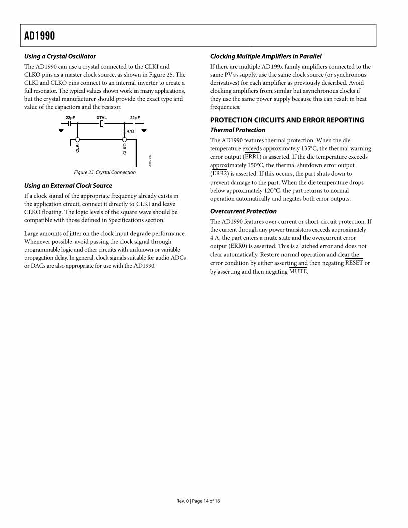
Using a Crystal Oscillator Clocking Multiple Amplifiers in Parallel
The AD1990 can use a crystal connected to the CLKI and CLKO pins as a master clock source, as shown in Figure 25. The CLKI and CLKO pins connect to an internal inverter to create a full resonator. The typical values shown work in many applications, but the crystal manufacturer should provide the exact type and value of the capacitors and the resistor.
If there are multiple AD199x family amplifiers connected to the same PVDD supply, use the same clock source (or synchronous derivatives) for each amplifier as previously described. Avoid clocking amplifiers from similar but asynchronous clocks if they use the same power supply because this can result in beat frequencies.
CLK
I
CLK
O
22pF 22pFXTAL
47Ω
0538
0-03
1
PROTECTION CIRCUITS AND ERROR REPORTING Thermal Protection
The AD1990 features thermal protection. When the die temperature exceeds approximately 135°C, the thermal warning error output (ERR1) is asserted. If the die temperature exceeds approximately 150°C, the thermal shutdown error output (ERR2) is asserted. If this occurs, the part shuts down to prevent damage to the part. When the die temperature drops below approximately 120°C, the part returns to normal operation automatically and negates both error outputs.
Figure 25. Crystal Connection
Using an External Clock Source
If a clock signal of the appropriate frequency already exists in the application circuit, connect it directly to CLKI and leave CLKO floating. The logic levels of the square wave should be compatible with those defined in Specifications section.
Overcurrent Protection
The AD1990 features over current or short-circuit protection. If the current through any power transistors exceeds approximately 4 A, the part enters a mute state and the overcurrent error output (ERR0) is asserted. This is a latched error and does not clear automatically. Restore normal operation and clear the error condition by either asserting and then negating RESET or by asserting and then negating MUTE.
Large amounts of jitter on the clock input degrade performance. Whenever possible, avoid passing the clock signal through programmable logic and other circuits with unknown or variable propagation delay. In general, clock signals suitable for audio ADCs or DACs are also appropriate for use with the AD1990.

AD1990
Rev. 0 | Page 15 of 16
APPLICATION CIRCUITS
OUTR+
NFR+
OUTR–
NFR–
0.1µF0.1µF
0.1µF
1000µF
PVDD
L
CR1
R2
OUTL+
NFL+
L
R1
R2
OUTL–
NFL–
C
L
CR1
R2
L
R1
R2
CERR0OVERCURRENT
ERR1THERMAL WARNING
ERR2THERMAL SHUTDOWN
AINL
AINR
REF_FILT
4.7µF 0.1µF
47µF
47µF
10µF
10µF
RESET
MUTE
DCTRL0
DCTRL1
DCTRL2
CLKI
CLKO
PGA1
PGA0
0.1µF1000µF
PVDD
AVDD
DVDD
AD1990
+
+
+
+
+
+
+
R1 = 4.2kΩR2 = 1.8kΩL = 18µHC = 1µFLOAD = 6Ω
DIGITALINPUTS
AVD
D
DVD
D
PVD
D1
PVD
D2
AG
ND
DG
ND
PGN
D1
PGN
D2
0538
0-03
2
Figure 26. Typical Application Circuit

AD1990
Rev. 0 | Page 16 of 16
OUTLINE DIMENSIONS
0.25 MIN
COMPLIANT TO JEDEC STANDARDS MO-220-VMMD-4
PIN 1INDICATOR
TOPVIEW
8.75BSC SQ
9.00BSC SQ
164
1617
4948
3233
0.450.400.35
0.50 BSC 0.20 REF
12° MAX 0.80 MAX0.65 TYP
1.000.850.80
7.50REF
0.05 MAX0.02 NOM
0.60 MAX0.60 MAX
EXPOSED PAD(BOTTOM VIEW)
0.300.250.18
SEATINGPLANE
PIN 1INDICATOR
7.257.10 SQ6.95
1221
05-0
Figure 27. 64-Lead Lead Frame Chip Scale Package [LFCSP_VQ]
9 mm × 9 mm Body, Very Thin Quad (CP-64-3)
Dimensions shown in millimeters
ORDERING GUIDE Model Temperature Range Package Description Package Option AD1990ACPZ1 −40°C to +85°C 64-Lead Lead Frame Chip Scale Package (LFCSP_VQ) CP-64-3 AD1990ACPZRL1 −40°C to +85°C 64-Lead Lead Frame Chip Scale Package (LFCSP_VQ), 13” Tape and Reel CP-64-3 AD1990ACPZRL71 −40°C to +85°C 64-Lead Lead Frame Chip Scale Package (LFCSP_VQ), 7” Tape and Reel CP-64-3 EVAL-AD1990EB Evaluation Board 1 Z = Pb-free part.
©2006 Analog Devices, Inc. All rights reserved. Trademarks and registered trademarks are the property of their respective owners. D05380-0-4/06(0)