Embed Size (px)
Citation preview
LOW
NO
ISE
AM
PLI
FIE
RS
- S
MT
1
HMC519LC4v04.1017
Gaas PHEMT MMIC LOW NOIsEaMPLIFIER, 18 - 31 GHz
For price, delivery, and to place orders: Analog Devices, Inc., One Technology Way, P.O. Box 9106, Norwood, MA 02062-9106Phone: 781-329-4700 • Order online at www.analog.comApplication Support: Phone: 1-800-ANALOG-D
Information furnished by Analog Devices is believed to be accurate and reliable. However, no responsibility is assumed by Analog Devices for its use, nor for any infringements of patents or other rights of third parties that may result from its use. Specifications subject to change without notice. No license is granted by implication or otherwise under any patent or patent rights of Analog Devices. Trademarks and registered trademarks are the property of their respective owners.
General Description
Features
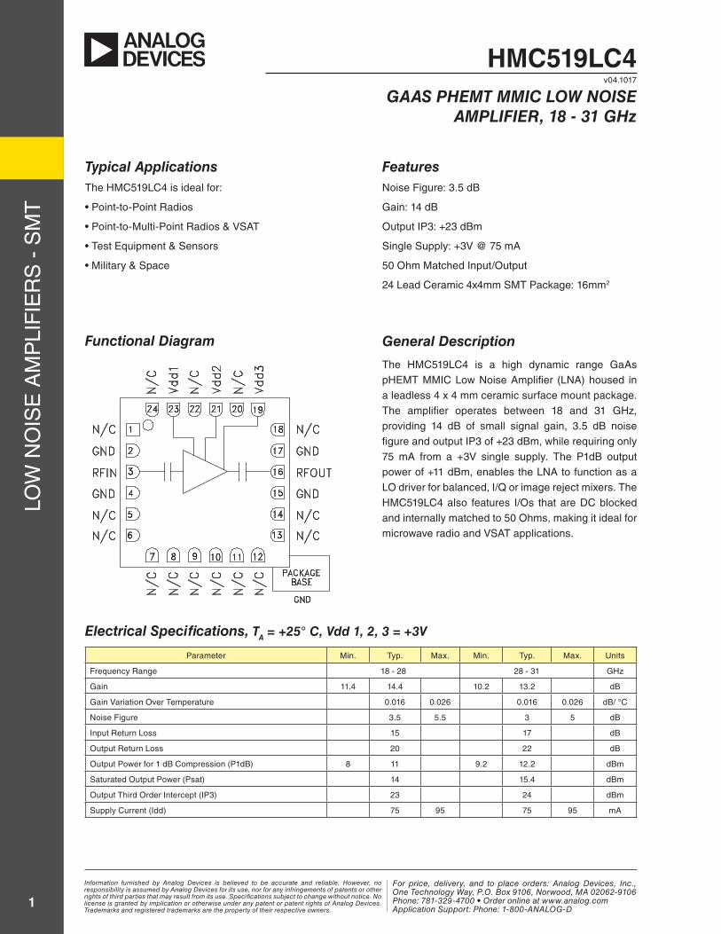
Functional Diagram
The HMC519LC4 is a high dynamic range GaAs pHEMT MMIC Low Noise Amplifier (LNA) housed in a leadless 4 x 4 mm ceramic surface mount package. The amplifier operates between 18 and 31 GHz, providing 14 dB of small signal gain, 3.5 dB noise figure and output IP3 of +23 dBm, while requiring only 75 mA from a +3V single supply. The P1dB output power of +11 dBm, enables the LNA to function as a LO driver for balanced, I/Q or image reject mixers. The HMC519LC4 also features I/Os that are DC blocked and internally matched to 50 Ohms, making it ideal for microwave radio and VSAT applications.
Noise Figure: 3.5 dB
Gain: 14 dB
Output IP3: +23 dBm
Single Supply: +3V @ 75 mA
50 Ohm Matched Input/Output
24 Lead Ceramic 4x4mm SMT Package: 16mm2
Electrical specifications, Ta = +25° C, Vdd 1, 2, 3 = +3V
Typical applicationsThe HMC519LC4 is ideal for:
• Point-to-Point Radios
• Point-to-Multi-Point Radios & VSAT
• Test Equipment & Sensors
• Military & Space
Parameter Min. Typ. Max. Min. Typ. Max. Units
Frequency Range 18 - 28 28 - 31 GHz
Gain 11.4 14.4 10.2 13.2 dB
Gain Variation Over Temperature 0.016 0.026 0.016 0.026 dB/ °C
Noise Figure 3.5 5.5 3 5 dB
Input Return Loss 15 17 dB
Output Return Loss 20 22 dB
Output Power for 1 dB Compression (P1dB) 8 11 9.2 12.2 dBm
Saturated Output Power (Psat) 14 15.4 dBm
Output Third Order Intercept (IP3) 23 24 dBm
Supply Current (Idd) 75 95 75 95 mA
LOW
NO
ISE
AM
PLI
FIE
RS
- S
MT
2
HMC519LC4v04.1017
Gaas PHEMT MMIC LOW NOIsEaMPLIFIER, 18 - 31 GHz
For price, delivery, and to place orders: Analog Devices, Inc., One Technology Way, P.O. Box 9106, Norwood, MA 02062-9106Phone: 781-329-4700 • Order online at www.analog.com
Application Support: Phone: 1-800-ANALOG-D
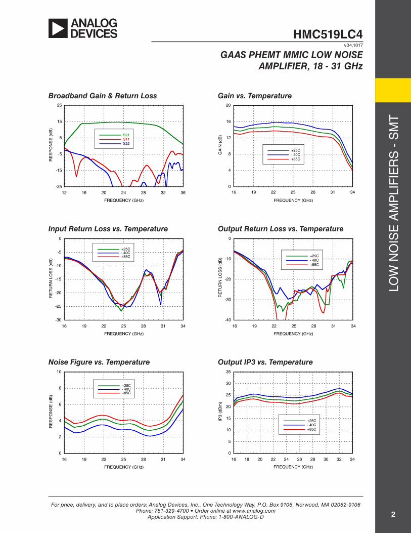
Input Return Loss vs. Temperature Output Return Loss vs. Temperature
Broadband Gain & Return Loss Gain vs. Temperature
Noise Figure vs. Temperature Output IP3 vs. Temperature
-25
-15
-5
5
15
25
12 16 20 24 28 32 36
S21S11S22
RE
SP
ON
SE
(dB
)
FREQUENCY (GHz)
-30
-25
-20
-15
-10
-5
0
16 19 22 25 28 31 34
+25C- 40C+85C
RE
TU
RN
LO
SS
(dB
)
FREQUENCY (GHz)
0
2
4
6
8
10
16 19 22 25 28 31 34
+25C- 40C+85C
RE
SP
ON
SE
(dB
)
FREQUENCY (GHz)
0
5
10
15
20
25
30
35
16 18 20 22 24 26 28 30 32 34
+25C- 40C
+85C
IP3 (
dB
m)
FREQUENCY (GHz)
-40
-30
-20
-10
0
16 19 22 25 28 31 34
+25C- 40C
+85C
RE
TU
RN
LO
SS
(dB
)
FREQUENCY (GHz)
0
4
8
12
16
20
16 19 22 25 28 31 34
+25C- 40C
+85C
GA
IN (
dB
)
FREQUENCY (GHz)
LOW
NO
ISE
AM
PLI
FIE
RS
- S
MT
3
HMC519LC4v04.1017
Gaas PHEMT MMIC LOW NOIsEaMPLIFIER, 18 - 31 GHz
For price, delivery, and to place orders: Analog Devices, Inc., One Technology Way, P.O. Box 9106, Norwood, MA 02062-9106Phone: 781-329-4700 • Order online at www.analog.com
Application Support: Phone: 1-800-ANALOG-D
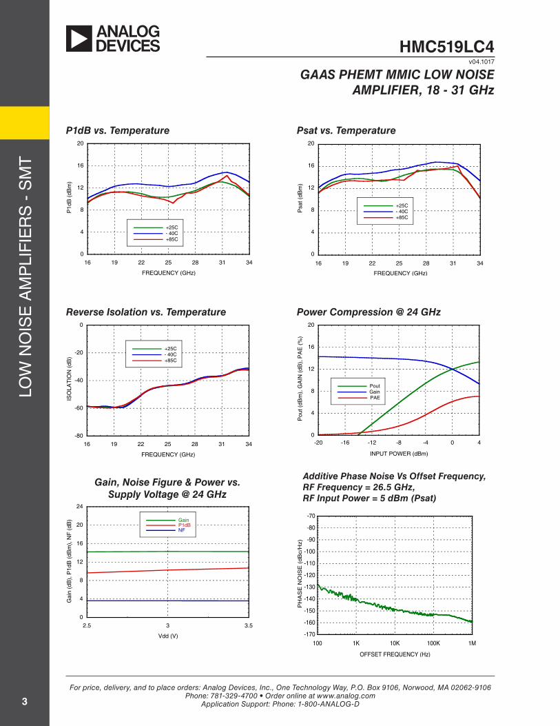
P1dB vs. Temperature
Power Compression @ 24 GHzReverse Isolation vs. Temperature
Psat vs. Temperature
Gain, Noise Figure & Power vs.supply Voltage @ 24 GHz
0
4
8
12
16
20
24
2.5 3 3.5
GainP1dBNF
Gain
(dB
), P
1dB
(dB
m),
NF
(dB
)
Vdd (V)
0
4
8
12
16
20
-20 -16 -12 -8 -4 0 4
PoutGain
PAE
Pout (d
Bm
), G
AIN
(dB
), P
AE
(%
)
INPUT POWER (dBm)
-80
-60
-40
-20
0
16 19 22 25 28 31 34
+25C- 40C+85C
ISO
LA
TIO
N (
dB
)
FREQUENCY (GHz)
0
4
8
12
16
20
16 19 22 25 28 31 34
+25C- 40C
+85C
Psat (d
Bm
)
FREQUENCY (GHz)
0
4
8
12
16
20
16 19 22 25 28 31 34
+25C- 40C
+85C
P1dB
(dB
m)
FREQUENCY (GHz)
-170
-160
-150
-140
-130
-120
-110
-100
-90
-80
-70
100 1K 10K 100K 1M
PH
AS
E N
OIS
E (
dB
c/H
z)
OFFSET FREQUENCY (Hz)
additive Phase Noise Vs Offset Frequency, RF Frequency = 26.5 GHz, RF Input Power = 5 dBm (Psat)
LOW
NO
ISE
AM
PLI
FIE
RS
- S
MT
4
HMC519LC4v04.1017
Gaas PHEMT MMIC LOW NOIsEaMPLIFIER, 18 - 31 GHz
For price, delivery, and to place orders: Analog Devices, Inc., One Technology Way, P.O. Box 9106, Norwood, MA 02062-9106Phone: 781-329-4700 • Order online at www.analog.com
Application Support: Phone: 1-800-ANALOG-D
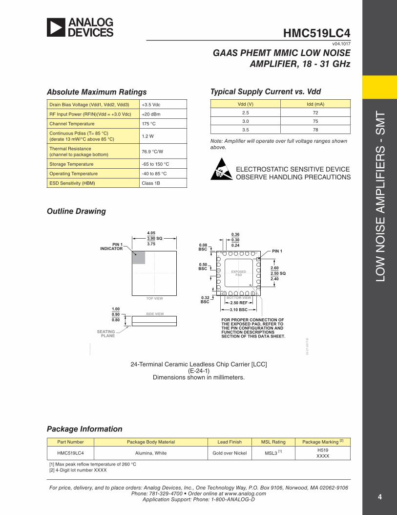
Outline Drawing
absolute Maximum RatingsDrain Bias Voltage (Vdd1, Vdd2, Vdd3) +3.5 Vdc
RF Input Power (RFIN)(Vdd = +3.0 Vdc) +20 dBm
Channel Temperature 175 °C
Continuous Pdiss (T= 85 °C)(derate 13 mW/°C above 85 °C)
1.2 W
Thermal Resistance (channel to package bottom)
76.9 °C/W
Storage Temperature -65 to 150 °C
Operating Temperature -40 to 85 °C
ESD Sensitivity (HBM) Class 1B
Vdd (V) Idd (mA)
2.5 72
3.0 75
3.5 78
Typical supply Current vs. Vdd
Note: Amplifier will operate over full voltage ranges shown above.
ELECTROSTATIC SENSITIVE DEVICEOBSERVE HANDLING PRECAUTIONS
Package Information
Part Number Package Body Material Lead Finish MSL Rating Package Marking [2]
HMC519LC4 Alumina, White Gold over Nickel MSL3 [1] H519XXXX
[1] Max peak reflow temperature of 260 °C[2] 4-Digit lot number XXXX
12
0.50BSC
2.50 REF
24-Terminal Ceramic Leadless Chip Carrier [LCC](E-24-1)
Dimensions shown in millimeters.
BOTTOM VIEWTOP VIEW
124
7
13
1819
6
02-2
7-20
17-B
0.360.300.24
EXPOSEDPAD
PKG
-004
840
PIN 1INDICATOR
4.053.90 SQ3.75
3.10 BSC
FOR PROPER CONNECTION OF THE EXPOSED PAD, REFER TO THE PIN CONFIGURATION AND FUNCTION DESCRIPTIONS SECTION OF THIS DATA SHEET.
2.602.50 SQ2.40
PIN 1
0.32BSC
0.08BSC
SIDE VIEW1.000.900.80
SEATINGPLANE
24-Terminal Ceramic Leadless Chip Carrier [LCC](E-24-1)
Dimensions shown in millimeters.
LOW
NO
ISE
AM
PLI
FIE
RS
- S
MT
5
HMC519LC4v04.1017
Gaas PHEMT MMIC LOW NOIsEaMPLIFIER, 18 - 31 GHz
For price, delivery, and to place orders: Analog Devices, Inc., One Technology Way, P.O. Box 9106, Norwood, MA 02062-9106Phone: 781-329-4700 • Order online at www.analog.com
Application Support: Phone: 1-800-ANALOG-D
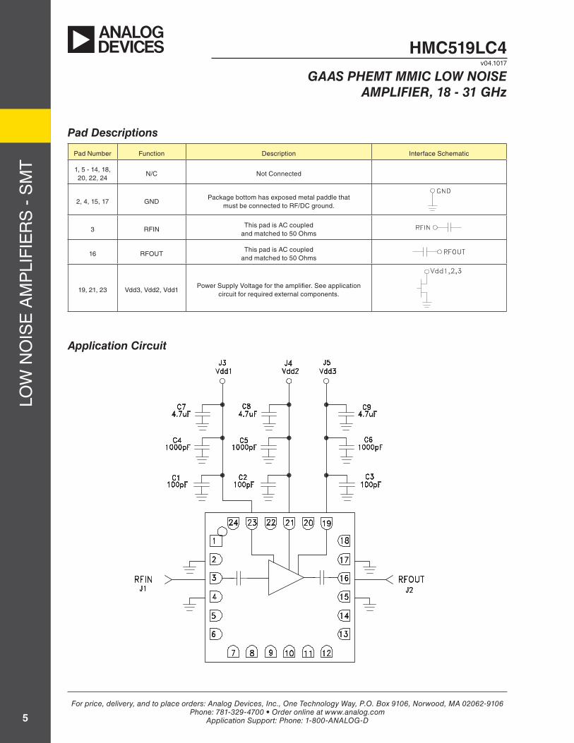
Pad Descriptions
Pad Number Function Description Interface Schematic
1, 5 - 14, 18, 20, 22, 24
N/C Not Connected
2, 4, 15, 17 GNDPackage bottom has exposed metal paddle that
must be connected to RF/DC ground.
3 RFINThis pad is AC coupled
and matched to 50 Ohms
16 RFOUTThis pad is AC coupled
and matched to 50 Ohms
19, 21, 23 Vdd3, Vdd2, Vdd1Power Supply Voltage for the amplifier. See application
circuit for required external components.
application Circuit
LOW
NO
ISE
AM
PLI
FIE
RS
- S
MT
6
HMC519LC4v04.1017
Gaas PHEMT MMIC LOW NOIsEaMPLIFIER, 18 - 31 GHz
For price, delivery, and to place orders: Analog Devices, Inc., One Technology Way, P.O. Box 9106, Norwood, MA 02062-9106Phone: 781-329-4700 • Order online at www.analog.com
Application Support: Phone: 1-800-ANALOG-D
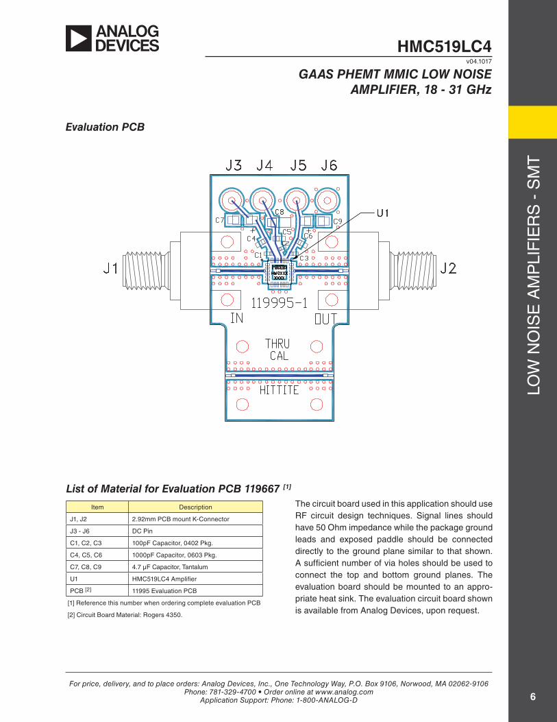
Item Description
J1, J2 2.92mm PCB mount K-Connector
J3 - J6 DC Pin
C1, C2, C3 100pF Capacitor, 0402 Pkg.
C4, C5, C6 1000pF Capacitor, 0603 Pkg.
C7, C8, C9 4.7 µF Capacitor, Tantalum
U1 HMC519LC4 Amplifier
PCB [2] 11995 Evaluation PCB
[1] Reference this number when ordering complete evaluation PCB
[2] Circuit Board Material: Rogers 4350.
List of Material for Evaluation PCB 119667 [1]
The circuit board used in this application should use RF circuit design techniques. Signal lines should have 50 Ohm impedance while the package ground leads and exposed paddle should be connected directly to the ground plane similar to that shown. A sufficient number of via holes should be used to connect the top and bottom ground planes. The evaluation board should be mounted to an appro-priate heat sink. The evaluation circuit board shown is available from Analog Devices, upon request.
Evaluation PCB


![BGU6101 Wideband silicon low-noise amplifier MMIC · Wideband silicon low-noise amplifier MMIC 7. Static characteristics Table 7. Static characteristics [1] ICC(tot) = ICC + IRF_OUT](https://img.dokumen.tips/doc/110x75/5f8bbe3820a0400a6155b583/bgu6101-wideband-silicon-low-noise-amplifier-mmic-wideband-silicon-low-noise-amplifier.jpg)


![RECENT PROGRESS IN 3D/MULTILAYER MMIC ... · Web viewLow loss [10] TI / Triquint Polyimide 25 m 1 Au GaAs PHEMT Low cost, PA, LNA [11] Toshiba BCB 10 m 1 Au GaAs PHEMT MM-wave MMIC](https://img.dokumen.tips/doc/110x75/6128664f46793703e6310aec/recent-progress-in-3dmultilayer-mmic-web-view-low-loss-10-ti-triquint-polyimide.jpg)