Embed Size (px)
Citation preview

Advanced Laser Bonding of Ultra Fine Pitch Cantilever Spring Pins for Assembly of Flash, DRAM and Logic Probe Cards
T. Teutsch, T. Oppert, A. Kolbasow

Overview• Introduction• Advantages on Laser Soldering• Cantilever Assembly & Laser Cutting
– Solder Balling / Solder Jetting– Laser Bonding of Cantilever– Specifications for laser Bonding Equipment– Design Rules– Vision System / Fiducial Alignment– Process Results / Examples
• Summary
2

Cantilever Bonding Video

Advantage of Laser BondingLocalized heat
No thermal stress on the areas outside of bondinginterface
Short Laser Pulse
Low thermal stress on chip (cantilever) / Substrate andinterconnection

Thermode Bonding vs Laser Bonding
Heating time vs bonding temperature:
Laser: 0.01 - 0.2 sec => msec Thermode: 1 – 10 sec=> sec Oven Reflow: 60 – 180 sec => min
Laser Thermode

Temperature Control
In Situ Laser Energy Tuning during Laser Bonding

Substrate Materials for Laser Soldering
Substrate
– FR4, BT- Epoxy, Polyimide, Ceramic, Silicon– TG above 150 ° C– most applications: rigid
Pad metallization– Copper with NiAu, Sn, Au– Thin Film : Cr/Au, NiAu, Au

Advantages for Probe Card Assembly
Flexibility Layout change by software only (no tooling) Parallel processing of multiple spring designs Independent from substrate material
Repair Capability Individual spring replacement No thermal influence on other springs
Customer Support Close to customer site

Cantilever Assembly Process FlowCantilever Design
Cantilever Manufacturing (Plating)
Cantilever Singulation (Laser Cutting)
Cantilever Inspection
Cantilever Sorting (into waffle packs) if needed
Substrate Solder Bumping, (solder paste dipping of cantilever can be integrated)
Cantilever / Substrate Alignment
Cantilever Laser Bonding
Cantilever inspection (optional)

Cantilever Assembly Line for Probe CardCantilever BonderLAPLACE-Can
Cantilever Sorter
Features Input: MEMS substrates Inspection of cantilever Laser cutting with the Laser Placement of cantilever in
waffle packs
Features Solder Jetting on
ceramic substrate Solder Balls sizes:
30 – 760 µm Solder alloys
capability:PbSn, SnAgCu or AuSn
Features Cantilever supplied in waffle packs Cantilever pick & rotation in vertical
position Substrate height measurement Dual camera for x, y alignment of
cantileverto the substrate
Probe tip z alignment Laser bonding of cantilever Post inspection Cantilever rework capability
SB2-Jet: Solder Jetting
11
Cantilever Cutting – Design Requirements

12
Cantilever Cutting – Design Requirements

13
Ball Reservoir Laser
Optical sensor
Pressure sensorN2
Optical sensors
CapillarySearch levelN2 gasReflowed
solder balls
Semiconductor wafer
Singulation Disk
Bond pad
Bond level
Schematic diagram of Solder Ball Bumping (SB²) process:
Soder Sphere Jetting
Solder Alloys: SAC, PbSn, AuSn, etc.

14
Process video for solder jetting
Solder Sphere Jetting
Solder depots placed on probe card substrate pads

- Linear axis or gantry system- Probe card sizes up to 14 inch- Alignment by precision optical system - Tip correction (bend)- Placement Accuracy: down to +/- 1.5µm
typ. +/- 3.0µm
- High power IR laser for bond reflow- Z height control- Cantilever thickness: 20µm – 100µm- Min. Pitch: 50µm- Process suitable for rework and complete card assembly- Post Bond inspection
Cantilever Bonder Specification

Cantilever Design Rules
Hump needed for handling and laser energy absorption– Hh ≥ 250 µm– Hw ≥ 250 µm
Tip base needed for alignment – Th ≥ 10 µm– Tw ≥ 10 µm

Pattern recognition & Fiducial Alignment
Automatic X,Y substrate alignment after loading and bond stage rotation (W-axis)
Pattern recognition with bond head camera
Alignment accuracy: +/- 1 µmHigh contrast simple mark
needed

Cantilever recognition inwaffle pack, R2R, or other carrier system– Pattern recognition of
whole cantilever– Detects position in waffle
pack pocket (A,B axis)– Discards defect cantilevers – Sensor: Camera 4 on Pick
& Flip unit– Alignment accuracy:
+/- 2.5 µm
Rotation and alignment for tool transfer
– Pattern recognition of whole cantilever
– Detects transfer offsets for bond tool (B,D,Z axis)
– Discards defect cantilevers– Sensor: Stationary Camera 2– Alignment accuracy:
+/- 2.5 µm, +/- 0.3°
Pattern recognition & Fiducial Alignment

Mechanical Correction
• Fitting of Cantilever into bond tool by touching down on a mechanical spring
• Force controlled
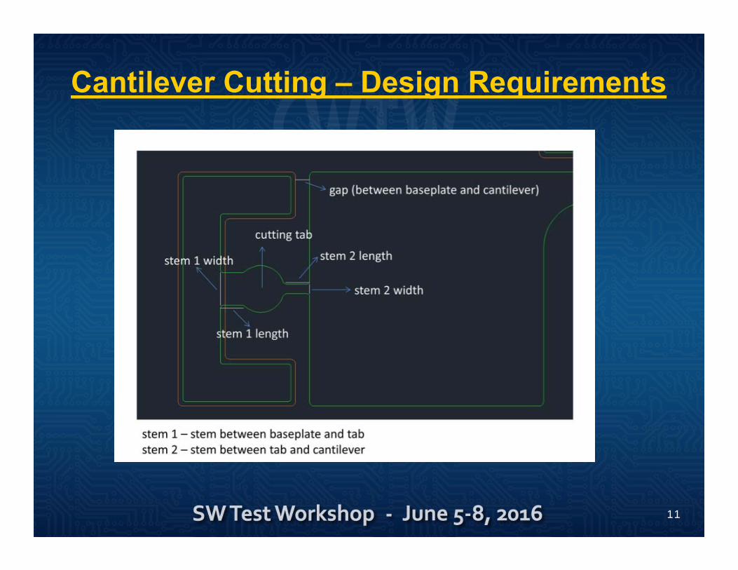
Optical Tip Alignment
An optical system determines– X offset for bonding– U angle correction– Tilt (hump bottom <‐> tip
base– Z‐offset for bonding
Two scans per measurement
+/- 0.01 µm optical scan repeatability
+/- 0.3 µm accuracy

Alignment Summary
Step Alignment procedure Corrected axis Sensor Measured featureAlignment Accuracy
1 Fiducial marks on substrate X, Y, W Bond head –Camera 1
100 µm high contrast circle or other geometrical shape
+/- 0.5 µm
2 Substrate height Z Laser Scanner or Touch Down
200 µm diameter height measurement mark or other location
+/- 0.05 µm (Laser)+/- 1 µm (Z-axis)
3 Detect cantilever in waffle pack A, B Pick & Flip Unit -Camera 4 Cantilever +/- 2.5 µm
4 Rotation and alignment for spring transfer Z, B, D Stationary
Camera 2 Cantilever+/- 2.5 µm+/-0.5°
5 Mechanical spring correction Z Mechanicalspring Force detection +/- 2 g
6 Optical scan alignment X, U, Z, Tilt Optical system Tip+/- 0.03 µm+/- 0.5 µm (axis)+/- 0.003°
7 Post bond hump/tip inspection X, Y Bond head –Camera 1 Hump or tip +/- 0.5 µm

Alignment Summary
Tip accuracy (machine capability):• in X +/- 1 µm• in Y +/- 1 µm• in Z +/- 2.5 µm
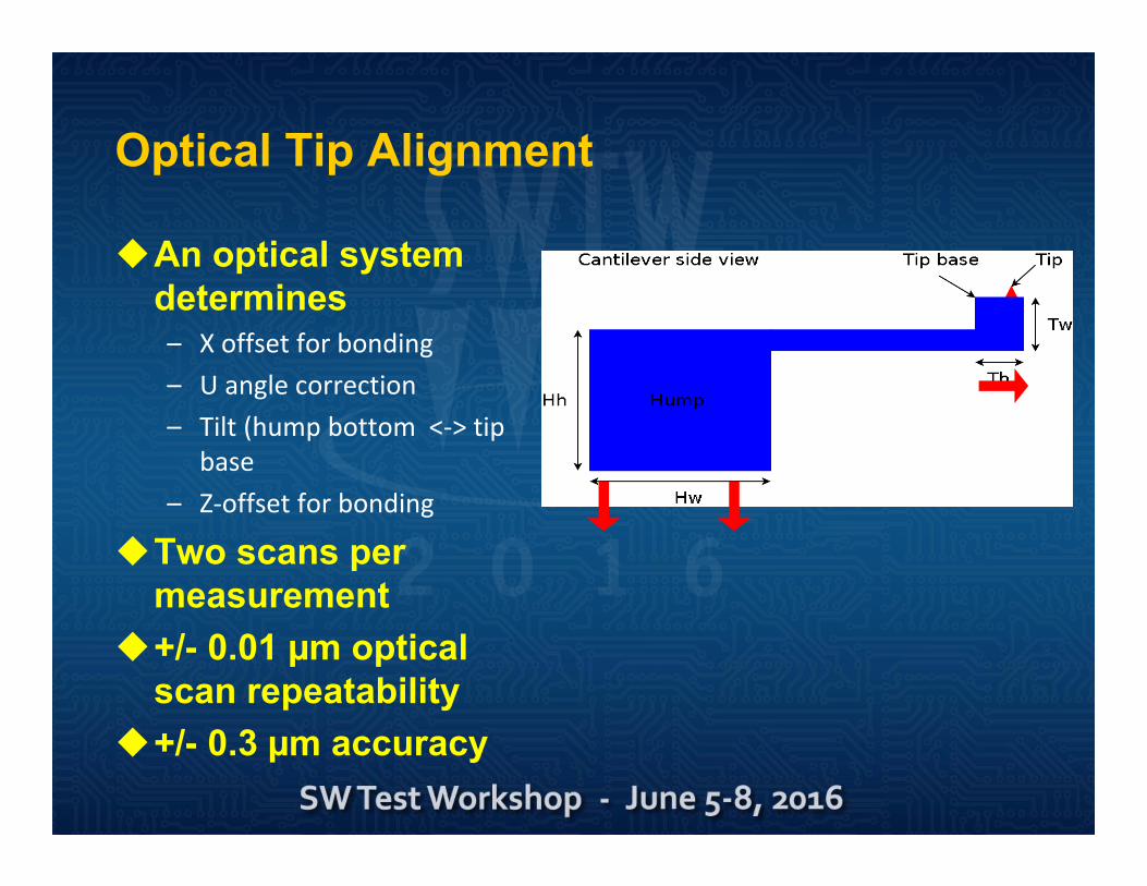
Post Bond Hump / Tip Inspection
• Sensor: Bond head camera 1
• Accuracy +/- 0.5 µm• Results used for smart
correction of next bond process
• Well defined edges for repeatable pattern detection needed

Cantilever Placement with LAPLACE-Can (80µm pitch)
Cantilever Bonding Results
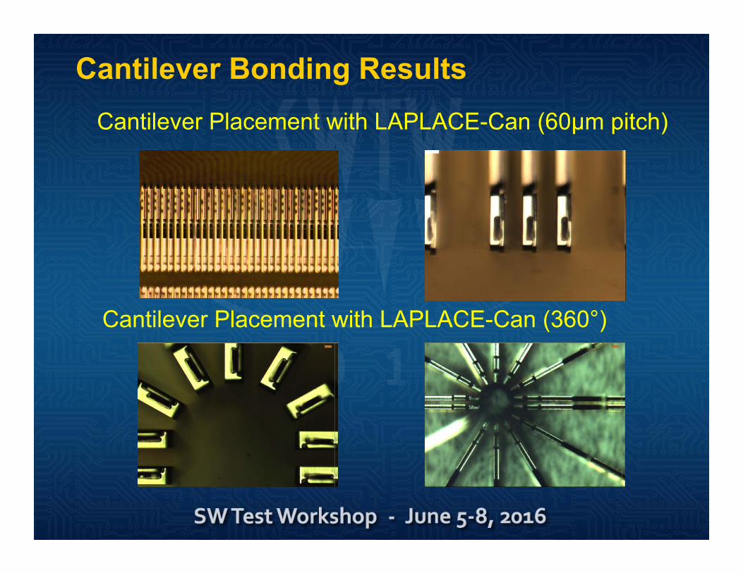
Cantilever Bonding ResultsCantilever Placement with LAPLACE-Can (60µm pitch)
Cantilever Placement with LAPLACE-Can (360°)
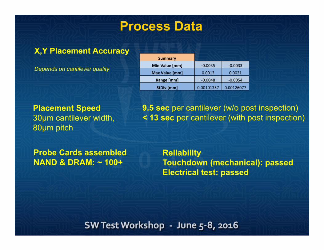
Process DataX,Y Placement Accuracy
Depends on cantilever quality
Summary
Min Value [mm] ‐0.0035 ‐0.0033
Max Value [mm] 0.0013 0.0021
Range [mm] ‐0.0048 ‐0.0054
StDiv [mm] 0.00101357 0.00126077
Placement Speed30μm cantilever width,80μm pitch
9.5 sec per cantilever (w/o post inspection)< 13 sec per cantilever (with post inspection)
Probe Cards assembledNAND & DRAM: ~ 100+
ReliabilityTouchdown (mechanical): passedElectrical test: passed

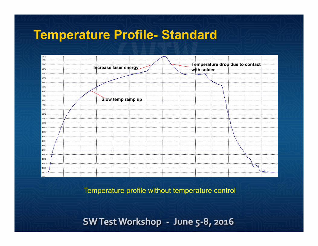
Temperature profile without temperature control
Slow temp ramp up
Increase laser energy Temperature drop due to contactwith solder
Temperature Profile- Current

Temperature profile with temperature control
Fast temp ramp up
Overshoot and readjust
Contact with solder
Hold temp
Post heating
Temperature Profile - Development

Substrate Height Measurement
Continuous substrate height measurement during bond process
Height check via touch down on substrate
Force resolution 5 g – 2000 gAlignment accuracy: +/- 1.5
µm (Z-axis)Measurement location on
UBM or other locations

4 measurement methodsForce (Standard)Accurate, but slow and touch of substrate
Laser (Triangulation)Accurate, contactless,but very sensitive to
surface roughnessLaser (Spectrometry)Accurate, fast and contactless
Laser (Confocal) Accurate, fast and contactless, small
measurement spot (in test for tip z-height)
Available Height Measurement Methods

Result – Substrate Height Measurements
Comparison Laser Measurement vs Force Measurement

Result of Substrate Height Measurement
Laser spectrometry & force reached nearly the sameresults. The maximum deviation was 3µm.
Percentage distribution of deviations for all measurements:
• 0µm: 46%• 1µm: 30%• 2µm: 22%• 3µm: 2%

Laplace-Can Test Run:Cantilever Positioning Accuracy
Positioning Accuracy Tip X Error [mm] Tip Y Error [mm]
Average 0,0002 0,0000Min Value -0,0033 -0,0021Max Value 0,0033 0,0026Range -0,0066 -0,0047
StDiv 0,001819 0,000970
Sample: 1000 cantilever, Pitch: 100µm

Cantilever Rework Video - Removal
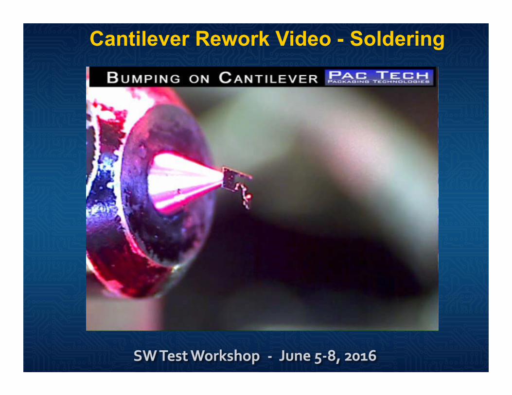
Cantilever Rework Video - Soldering

Summary
• A new laser assisted sequential cantilever attach process has been presented
• Placement accuracies down to +/-1 μm in X,Y have been demonstrated
• Assembly throughput of 9.5 sec per spring has been observed• Probe springs can be assembled with free 360 deg orientation• A fine pitch capability down to 50μm has been accomplished• The assembly process is capable of single spring rework

Complete process cycle time incl. Laser: 9,5sec
Process Cycle time
Temperature profile without temperature control
Slow temp ramp up
Increase laser energy Temperature drop due to contactwith solder
Temperature Profile- Standard

Temperature profile with temperature control
Fast temp ramp up
Overshoot and readjust
Contact with solder
Hold temp
Post heating
Temperature Profile - Improved

4 measurement methodsForce (Standard)Accurate, but slow and touch of substrate
Laser (Triangulation)Accurate, contactless,but very sensitive to
surface roughnessLaser (Spectrometry)Accurate, fast and contactless
Laser (Confocal) Accurate, fast and contactless, small
measurement spot (in test for tip z-height)
Height Measurement

Result – Substrate Height Measurements
Comparison Laser Measurement vs Force Measurement

Result of Substrate Height Measurement
Laser spectrometry & force reached nearly the sameresults. The maximum deviation was 3µm.
Percentage distribution of deviations for all measurements:
• 0µm: 46%• 1µm: 30%• 2µm: 22%• 3µm: 2%

Mean values per chip
Result – Height Measurements

44
Cantilever Cutting – Design Requirements

45
Cantilever Cutting – Design Requirements

Pattern recognition & Fiducial Alignment
Automatic X,Y substrate alignment after loading and bond stage rotation (W-axis)
Pattern recognition with bond head camera
Alignment accuracy: +/- 1 µmHigh contrast simple mark
needed

Cantilever recognition inwaffle pack, R2R, or other carrier system– Pattern recognition of
whole cantilever– Detects position in waffle
pack pocket (A,B axis)– Discards defect cantilevers – Sensor: Camera 4 on Pick
& Flip unit– Alignment accuracy:
+/- 2.5 µm
Rotation and alignment for tool transfer
– Pattern recognition of whole cantilever
– Detects transfer offsets for bond tool (B,D,Z axis)
– Discards defect cantilevers– Sensor: Stationary Camera 2– Alignment accuracy:
+/- 2.5 µm, +/- 0.3°
Pattern recognition & Fiducial Alignment

Mechanical Correction
• Fitting of Cantilever into bond tool by touching down on a mechanical spring
• Force controlled