Embed Size (px)
Citation preview

4.25 Gbps, 3.3 V Low Noise, Transimpedance Amplifier
Data Sheet ADN2882
FEATURES Bandwidth: 3.5 GHz Input noise current density: 8 pA/√Hz Optical sensitivity
−22.0 dBm1 −20.4 dBm2
Differential transimpedance: 3700 V/A Power dissipation: 80 mW Differential output swing: 260 mV p-p Input overload current: 5.6 mA p-p On-chip RSSI function Low frequency cutoff: 12 kHz On-chip PD filter: RF = 200 Ω, CF = 20 pF Die size: 0.7 mm × 1.2 mm
APPLICATIONS 4.25 Gbps optical receivers GbE/FC optical receivers SFF-8472-compliant receivers PIN/APD-TIA receiver optical subassemblies
GENERAL DESCRIPTION The ADN2882 is a 3.3 V high gain SiGe transimpedance amplifier (TIA) which converts the small signal current of a photo detector to a large differential voltage output. The ADN2882 features a typical 475 nA input-referred noise, enabling an optical sensitivity of −22 dBm (0.85 A/W PIN). With a bandwidth of 3.5 GHz, the ADN2882 allows a data rate operation up to 4.25 Gbps. Typical power dissipation is 80 mW.
To facilitate the assembly in small form factor packages, such as TO-46 headers, the ADN2882 provides an on-chip RC filter (200 Ω, 20 pF) and features a 12 kHz low frequency cutoff without using an external capacitor. An on-chip RSSI circuit, which generates a voltage proportional to the average photo-diode current, is available for power monitoring and assembly alignment.
The ADN2882 is available in die form. With a chip area of 1.2 mm × 0.7 mm, the TIA layout is optimized for TO-Can-based packages.
1 Based on 1550 nm PIN, CD = 0.5 ± 0.10 pF, responsivity = 0.85 A/W, ER = 9 dB, PRBS 231 − 1 at 4.25 Gbps, BER < 10−12.
2 Calculated result based on an 850 nm PIN, CD = 0.5 ± 0.15 pF, responsivity = 0.48 A/W, ER = 9 dB, at 4.25 Gbps, BER < 10−12.
FUNCTIONAL BLOCK DIAGRAM
1100Ω
0.85V20pF
50Ω200Ω 50Ω
3.3V
FILTER
IN
VCCFILTER VCC
GND GND CAP
5mA
OUTBOUT
RSSI
0494
6-00
1
Figure 1.
Rev. A Document Feedback Information furnished by Analog Devices is believed to be accurate and reliable. However, no responsibility is assumed by Analog Devices for its use, nor for any infringements of patents or other rights of third parties that may result from its use. Specifications subject to change without notice. No license is granted by implication or otherwise under any patent or patent rights of Analog Devices. Trademarks and registered trademarks are the property of their respective owners.
One Technology Way, P.O. Box 9106, Norwood, MA 02062-9106, U.S.A. Tel: 781.329.4700 ©2005–2014 Analog Devices, Inc. All rights reserved. Technical Support www.analog.com
OBSOLETE

ADN2882 Data Sheet
TABLE OF CONTENTS Features .............................................................................................. 1 Applications ....................................................................................... 1 General Description ......................................................................... 1 Functional Block Diagram .............................................................. 1 Revision History ............................................................................... 2 Specifications ..................................................................................... 3 Absolute Maximum Ratings ............................................................ 4
ESD Caution .................................................................................. 4
Pin Layout and Function Descriptions ...........................................5 Typical Performance Characteristics ..............................................6 5-Pin TO-46 Assembly Recommendations ...................................9 4-Pin TO-46 Assembly Recommendations ................................ 11 Outline Dimensions ....................................................................... 12
Die Information .......................................................................... 12 Ordering Guide .......................................................................... 12
REVISION HISTORY 9/14—Rev. 0 to Rev. A
Changes to Figure 19 ........................................................................ 9 Changes to Figure 22 ...................................................................... 10 Changes to Ordering Guide .......................................................... 12
6/05—Revision 0: Initial Version
Rev. A | Page 2 of 12
OBSOLETE

Data Sheet ADN2882
Rev. A | Page 3 of 12
SPECIFICATIONS Minimum/maximum VCC = 3.3 V ± 0.3 V, TAMBIENT = −40°C to +95°C; typical VCC = 3.3 V, TAMBIENT = 25°C, unless otherwise noted.
Table 1. Parameter Conditions Min Typ Max Unit DYNAMIC PERFORMANCE
Bandwidth (BW)1 −3 dB 2.9 3.5 GHz Total Input Referred RMS Noise (IRMS) CD = 0.5 pF, 4.0 GHz low-pass filter 475 605 nA Small Signal Transimpedance (ZT)1 100 MHz, differential 2800 3700 4800 V/A 100 MHz, single-ended 1400 1850 2400 V/A Low Frequency Cutoff IIN = 20 μA, CAP open 12 kHz IIN = 500 μA, CAP open 84 kHz Output Return Loss DC to 4.0 GHz, differential −25 dB Input Overload Current ER = 10 dB 3.5 5.6 mA p-p Maximum Differential Output Swing IIN, P-P = 2.0 mA 170 260 375 mV p-p Output Data Transition Time IIN, P-P = 1.0 mA; 20% to 80% rise/fall time 46 ps PSRR IIN = 0 mA, 1 MHz < frequency <10 MHz 40 dB Group Delay Variation 1.0 GHz to 4.0 GHz ±12 ps Transimpedance Ripple 50 MHz to 1.0 GHz, single-ended 0.5 dB Deterministic Jitter 10 μA < IIN, P-P ≤ 100 μA, K28.5 @ 4.25 Gbps 8 ps p-p 100 μA < IIN, P-P ≤ 1.0 mA, K28.5 @ 4.25 Gbps 15 ps p-p Linear Output Range Differential output, <1 dB compression 190 mV p-p Linear Input Current Range Single-ended input, <1 dB compression 45 μA p-p
DC PERFORMANCE Power Dissipation IIN, AVE = 0 80 110 mW Input Voltage Compliance voltage 0.85 V Output Common-Mode Voltage DC (50 Ω) terminated to VCC VCC − 0.12 V Output Impedance Single-ended 50 Ω PD Filter Resistance RF 200 Ω PD Filter Capacitance CF 20 pF RSSI Gain IIN, AVE = 5 μA to 1 mA 0.83 V/mA RSSI Offset IIN, AVE = 10 μA 4.6 mV RSSI Accuracy 5 μA < IIN, P-P ≤ 20 μA ±9 % 20 μA < IIN, P-P ≤ 1 mA ±3 %
1 A signal current equivalent to IIN P-P = 10 μA is applied to the TIA input. No input capacitor is applied.
OBSOLETE

ADN2882 Data Sheet
ABSOLUTE MAXIMUM RATINGS Table 2. Parameter Rating Supply Voltage (VCC to GND) 5 V Maximum Voltage to All Input and
Output Signal Pins VCC + 0.4 V
Minimum Voltage to All Input and Output Signal Pins
GND − 0.4 V
Maximum Input Current 10 mA Storage Temperature Range −65°C to +125°C Operating Ambient Temperature Range −40°C to +95°C Maximum Junction Temperature 125°C Die Attach Temperature (<30 sec) 410°C
Stresses above those listed under Absolute Maximum Ratings may cause permanent damage to the device. This is a stress rating only; functional operation of the device at these or any other conditions above those indicated in the operational section of this specification is not implied. Exposure to absolute maximum rating conditions for extended periods may affect device reliability.
ESD CAUTION
Rev. A | Page 4 of 12
OBSOLETE

Data Sheet ADN2882
PIN LAYOUT AND FUNCTION DESCRIPTIONS
2
3
4
5 6 7 8 9
11
12
1 1314151617GND
IN
TEST
FILTER
FILTER GND
OUTB
OUT
GND
10
GNDCAPRSSIGND
VCC VCC VCCFILTER GND
0494
6-00
2
Figure 2. Pad Layout
Table 3. Pad Function Descriptions Pad No. Mnemonic Pin Type1 Description
1 GND P Ground. (Input return.) 2 IN AI Current Input. Bond directly to a photodiode (PD) anode. 3 TEST AI Test Probe Pad. Do not connect.
4 FILTER AO Filter Output. Pad 4 and Pad 5 are metal connected. Optional bond to a PD cathode. 5 FILTER AO Filter Output. Pad 4 and Pad 5 are metal connected. Optional bond to a PD cathode. 6 GND P Ground. 7 RSSI AO Voltage Output. Provides average input current monitoring. Leave it open, if not used.
8 CAP AI Leave This Pin Open for Non-SONET Applications. For SONET applications, see Figure 10 and contact sales for assembly details.
9 GND P Ground. (Output return.) 10 GND P Ground. (Output return.)
11 OUTB AO Negative Output, CML, On-Chip 50 Ω Termination (AC or DC Termination). 12 OUT AO Positive Output, CML, On-Chip 50 Ω Termination (AC or DC Termination). 13 GND P Ground. (Output return.) 14 GND P Ground. (Output return.)
15 VCCFILTER P On-Chip Filter Supply. Connect to VCC to Enable On-Chip RC Filter (200 Ω, 20 pF). Leave it open, if not used.
16 VCC P 3.3 V Power Supply. Place a 200 pF, RF decoupling capacitor close to the power pad to reduce the power noise.
17 VCC P 3.3 V Power Supply. Place a 200 pF, RF decoupling capacitor close to the power pad to reduce the power noise.
1 P = power; AI = analog input; and AO = analog output.
Rev. A | Page 5 of 12
OBSOLETE
ADN2882 Data Sheet
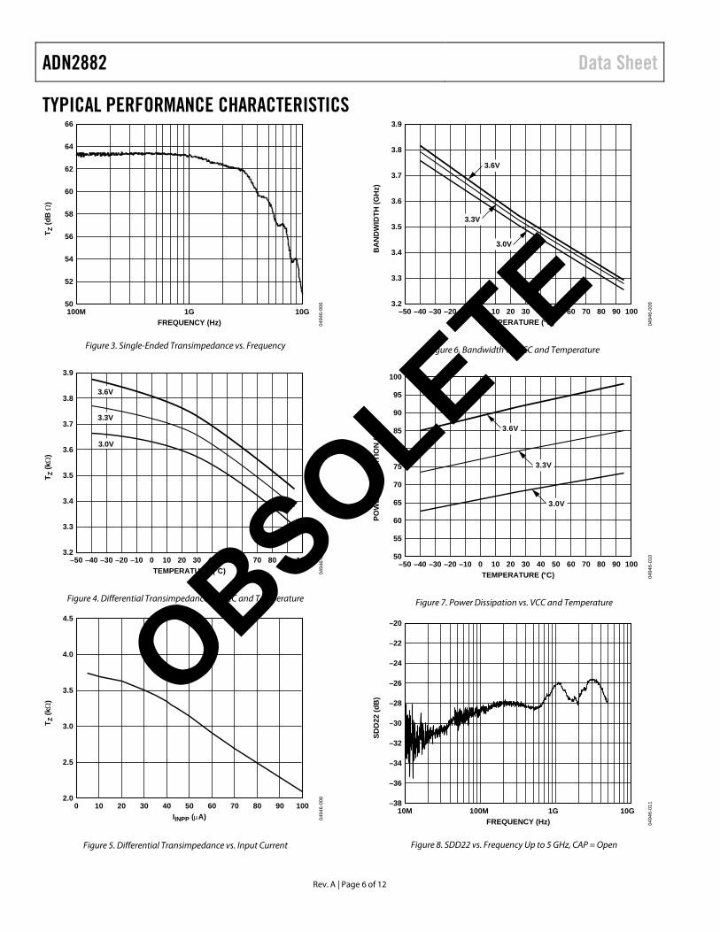
TYPICAL PERFORMANCE CHARACTERISTICS
0494
6-00
6FREQUENCY (Hz)
10G100M 1G
T Z (d
BΩ
)
66
64
62
60
58
56
54
52
50
Figure 3. Single-Ended Transimpedance vs. Frequency
0494
6-00
7
TEMPERATURE (°C)100–50 –40 –30 –20 –10 0 10 20 30 40 50 60 70 80 90
T Z (k
Ω)
3.9
3.7
3.8
3.6
3.4
3.5
3.3
3.2
3.0V
3.3V
3.6V
Figure 4. Differential Transimpedance vs. VCC and Temperature
0494
6-00
8
IINPP (µA)1000 10 20 30 40 50 60 70 80 90
T Z (k
Ω)
4.5
4.0
3.5
3.0
2.5
2.0
Figure 5. Differential Transimpedance vs. Input Current
0494
6-00
9
TEMPERATURE (°C)100–50 –20 10 60–40 –10 30–30 0 5040 907020 80
BA
ND
WID
TH (G
Hz)
3.9
3.8
3.7
3.6
3.5
3.4
3.3
3.2
3.0V
3.6V
3.3V
Figure 6. Bandwidth vs. VCC and Temperature
0494
6-01
0
TEMPERATURE (°C)100–50 –40 –30 –20 –10 0 10 20 30 40 50 60 70 80 90
3.0V
3.3V
3.6V
POW
ER D
ISSI
PATI
ON
(mW
)100
95
90
85
80
75
70
65
60
55
50
Figure 7. Power Dissipation vs. VCC and Temperature
0494
6-01
1
FREQUENCY (Hz)10G10M 100M 1G
SDD
22 (d
B)
–20
–22
–26
–24
–28
–30
–32
–34
–36
–38
Figure 8. SDD22 vs. Frequency Up to 5 GHz, CAP = Open
Rev. A | Page 6 of 12
OBSOLETE

Data Sheet ADN2882
0494
6-01
2
IIN (µA)11000 100 200 300 400 500 600 700 800 900 1000
LOW
FR
EQU
ENC
Y C
UTO
FF (k
Hz)
100
70
80
90
50
60
30
40
10
20
0
Figure 9. Low Frequency Cutoff vs. Input Current (CAP = OPEN) 04
946-
033
EXTERNAL CAPACITANCE AT CAP (pF)10,0001 10 100 1,000
LOW
FR
EQU
ENC
Y C
UTO
FF (k
Hz)
16
14
12
10
8
6
4
2
0
Figure 10. Low Frequency Cutoff vs. External Capacitance at CAP
0494
6-01
3
IIN (µA)50000 500 1000 1500 2000 2500 3000 3500 4000 4500
V RSS
I (m
V)
3000
2500
1500
2000
1000
500
0
Figure 11. Full-Scale of RSSI Voltage Output vs. Input Current
0494
6-01
5
IIN (µA)300 5 10 15 20 25
V RSS
I (m
V)
25
20
15
10
5
0
Figure 12. RSSI Voltage Output vs. Input Current (0 µA to 30 µA)
0494
6-01
6
PHOTODIODE CAPACITANCE CD (pF)1.00 0.2 0.4 0.6 0.8
INPU
T R
EFER
RED
RM
S N
OIS
E (n
A)
700
600
500
400
300
Figure 13. Input Referred Noise (DC to 4.0 GHz) vs. PD Capacitance
0494
6-01
7
TEMPERATURE (°C)100–50 0 50
INPU
T R
EFER
RED
NO
ISE
(nA
)
540
520
480
500
460
420
440
400CD = 0.5pF
Figure 14. Input Referred Noise vs. Temperature
Rev. A | Page 7 of 12
OBSOLETE

ADN2882 Data Sheet
0494
6-01
8
FREQUENCY (GHz)51 2 3 4
GR
OU
P D
ELA
Y (p
s)
100
50
–50
0
–100
Figure 15. Group Delay vs. Frequency 04
946-
019
40ps/DIVOPTICAL POWER –21.8dBm
4.7m
V/D
IV
Figure 16. Output Eye at 4.25 Gbps (1550 nm PD with Responsivity = 0.85 A/W,
ER = 9 dB, PRBS 231 − 1, BER < 10−12)
0494
5-02
6
IIN AVERAGE (mA)1.000.01 0.10
DET
ERM
INIS
TIC
JIT
TER
(pS)
20
16
18
14
12
6
8
10
4
2
0
–40°C25°C
85°C
Figure 17. Deterministic Jitter vs. Input Current (K28.5 @ 4.25 Gbps)
Rev. A | Page 8 of 12
OBSOLETE

Data Sheet ADN2882
5-PIN TO-46 ASSEMBLY RECOMMENDATIONS Contact sales for more details.
0494
6-00
3
CPD
CB
VPD VCC
OUTB OUT
Figure 18. 5-Pin TO-46 with External Photodiode Supply VPD
ADN2882PD
CB
CPD
0494
6-03
1
Figure 19. Side View of the Assembly
0.85V20pF
50Ω200Ω 50Ω
VCC
CB
CPD
FILTER
IN
VCC
GND GND CAP
OUTBOUT
RSSI
VPD
B.W B.W.
B.W. B.W.
B.W.
B.W.
B.W. B.W.
B.W.
B.W.
0494
6-02
7
Figure 20. Equivalent Circuit of Assembly Including Bond Wires
Table 4. Bill of Materials (BOM) Component Description PD 1× vendor specific, 4.25 Gbps, photodiode TIA 1× ADN2882 (0.7 mm × 1.2 mm), 4.25 Gbps,
transimpedance amplifier CB 1× 200 pF, RF single-layer capacitor CPD 1× 560 pF, RF single-layer capacitor
Notes
One mil thickness gold wire, ball bond recommended.
Minimize all GND bond-wire lengths.
Minimize IN, FILTER, OUT, and OUTB bond-wire lengths.
Maintain symmetry in length and orientation between OUT and OUTB bond wires.
Maintain symmetry between IN/FILTER and OUT/OUTB bond wires.
Rev. A | Page 9 of 12
OBSOLETE

ADN2882 Data Sheet
0494
6-02
3
CB
VCC
OUTB OUT
SC
RSSI
Figure 21. 5-Pin TO-46 with Internal PD Biasing and RSSI Output
ADN2882PD
CBSC
0494
6-03
2
Figure 22. Side View of the Assembly
0.85V20pF
50Ω200Ω 50Ω
VCC
CB
FILTER
IN
VCCVCCFILTER
GND GND CAP
OUTBOUT
RSSI
0494
6-02
8
B.W.B.W.
B.W.
B.W.
B.W.
B.W. B.W.
B.W.
B.W.
B.W.
Figure 23. Equivalent Circuit of the Assembly Including Bond Wires
Table 5. Bill of Materials (BOM) Component Description PD 1× vendor specific, 4.25 Gbps, photodiode TIA 1× ADN2882 (0.7 mm × 1.2 mm), 4.25 Gbps,
transimpedance amplifier CB 1× 200 pF, RF single-layer capacitor SC 1× ceramic standoff or 1× optional capacitor
Notes
One mil thickness gold wire, ball bond recommended.
Minimize all GND bond-wire lengths.
Minimize IN, FILTER, OUT, and OUTB bond-wire lengths.
Maintain symmetry in length and orientation between OUT and OUTB bond wires.
Maintain symmetry between IN/FILTER and OUT/OUTB bond wires.
Rev. A | Page 10 of 12
OBSOLETE

Data Sheet ADN2882
Rev. A | Page 11 of 12
4-PIN TO-46 ASSEMBLY RECOMMENDATIONS Contact sales for more details.
SC
CB
VCC
OUTOUTB
0494
6-00
4
Figure 24. 4-Pin TO-46 with Internal PD Biasing
ADN2882 PD
SC
0494
6-03
0
TO CAN HEADER
CB
Figure 25. Side View of the Assembly
0.85V20pF
50200 50
FILTER
IN
VCC
GND GND CAP
OUTBOUT
RSSI
0494
6-02
9
VCC
CB
VCCFILTER
B.W.
B.W.
B.W.
B.W.
B.W.
B.W. B.W.
B.W.
B.W.
Figure 26. Equivalent Circuit of Assembly Including Bond Wires
Table 6. Bill of Materials (BOM) Component Description PD 1× vendor specific, 4.25 Gbps, photodiode TIA 1× ADN2882 (0.7 mm × 1.2 mm), 4.25 Gbps,
transimpedance amplifier CB 1× 200 pF, RF single-layer capacitor SC 1× ceramic standoff or 1× optional capacitor
Notes
One mil thickness gold wire, ball bond recommended.
Minimize all GND bond-wire lengths.
Minimize IN, FILTER, OUT, and OUTB bond-wire lengths.
Maintain symmetry in length and orientation between OUT and OUTB bond wires.
Maintain symmetry between IN/FILTER and OUT/OUTB bond wires.
OBSOLETE

ADN2882 Data Sheet
Rev. A | Page 12 of 12
OUTLINE DIMENSIONS
1.20
0.70
1
2
3
4
5 6 7 8 10
13151617
9
14
11
12
TOP VIEW
SIDE VIEW 0.25 Figure 27. 17-Pad Bare Die Sales [CHIP]
C-17-1 Dimensions shown in millimeters
Table 7. Pad Coordinates Pad No. Mnemonic X (μm) Y (μm) 1 GND −500 +260 2 IN −500 +130 3 TEST −500 +10 4 FILTER −500 −120 5 FILTER −500 −260 6 GND −350 −260 7 RSSI −200 −260 8 CAP −50 −260 9 GND +130 −260 10 GND +500 −260 11 OUTB +350 −60 12 OUT +350 +60 13 GND +500 +260 14 GND +130 +260 15 VCCFILTER −50 +260 16 VCC −200 +260 17 VCC −350 +260
DIE INFORMATION Die Size
0.7 mm × 1.2 mm (edge to edge, including 1 mil scribe)
Die Thickness
10 mils = 0.25 mm
Passivation Openings
0.075 mm × 0.075 mm (Pad 1 to 8, 10, 13, and Pad 15 to 17)
0.144 mm × 0.075 mm (Pad 9, 11, 12, and Pad 14)
Passivation Composition
5000 Å Si3N4 (top)
5000 Å SiO2 (bottom)
Pad Composition
Al/1%Cu
Substrate Contact
To ground
ORDERING GUIDE Model Temperature MOQ Description1 Package Option ADN2882ACHIPS −40°C to +95°C 200 17-Pad Die Sales C-17-1 ADN2882A-DF −40°C to +95°C 5,704 Reconstituted die on 8” metal film frame
1 Contact Analog Devices, Inc., sales for more information on the film frame ADM2882A-DF.
©2005–2014 Analog Devices, Inc. All rights reserved. Trademarks and registered trademarks are the property of their respective owners. D04946-0-9/14(A)
OBSOLETE


![tsushou.co.jptsushou.co.jp/products/elemac_sheet.pdf · MA 9 -f 50 40 30 20 10 10 100 [MHz] 1000 1000 (SA9-f20) 10 100 MHz] MA9-f70 1000 100 80 -0 60 20 30 100 [MHz] SAÐ-DO](https://img.dokumen.tips/doc/110x75/5b5badbc7f8b9a01748e927b/-ma-9-f-50-40-30-20-10-10-100-mhz-1000-1000-sa9-f20-10-100-mhz-ma9-f70.jpg)