Embed Size (px)
Citation preview

NATIONAL RADIO ASTRONOMY OBSERVATORY
CHARLOTTESVILLE, VIRGINIA
ELECTRONICS DIVISION INTERNAL REPORT No. 263
BREADBOARD 100 MHz PHASE-SHIFTER FOR
INTERFEROMETER LOBE-ROTATION
JOSEPH GREENBERG
AUGUST 1986
NUMBER OF COPIES: 150
BREADBOARD 100 MHZ PHASE-SHIFTER FORINTERFEROMETER LOBE-ROTATION
Joseph Greenberg
TABLE OF CONTENTS
• • • • • • 0 • • • • • • • . .
• • • • • • • • • • • • • •
FIGURESFIGURES
• • • • • 0 • • • • • • • • • •
TABLESTABLESTABLES
Table I NCO Output Frequencies in Hz . . . . . . . . . . . . . . 13NCO Output Frequencies in Hz . . . . . . . . . . . . . . 13NCO Output Frequencies in Hz . . . . . . . . . . . . . . 13NCO Output Frequencies in Hz . . . . . . . . . . . . . . 13
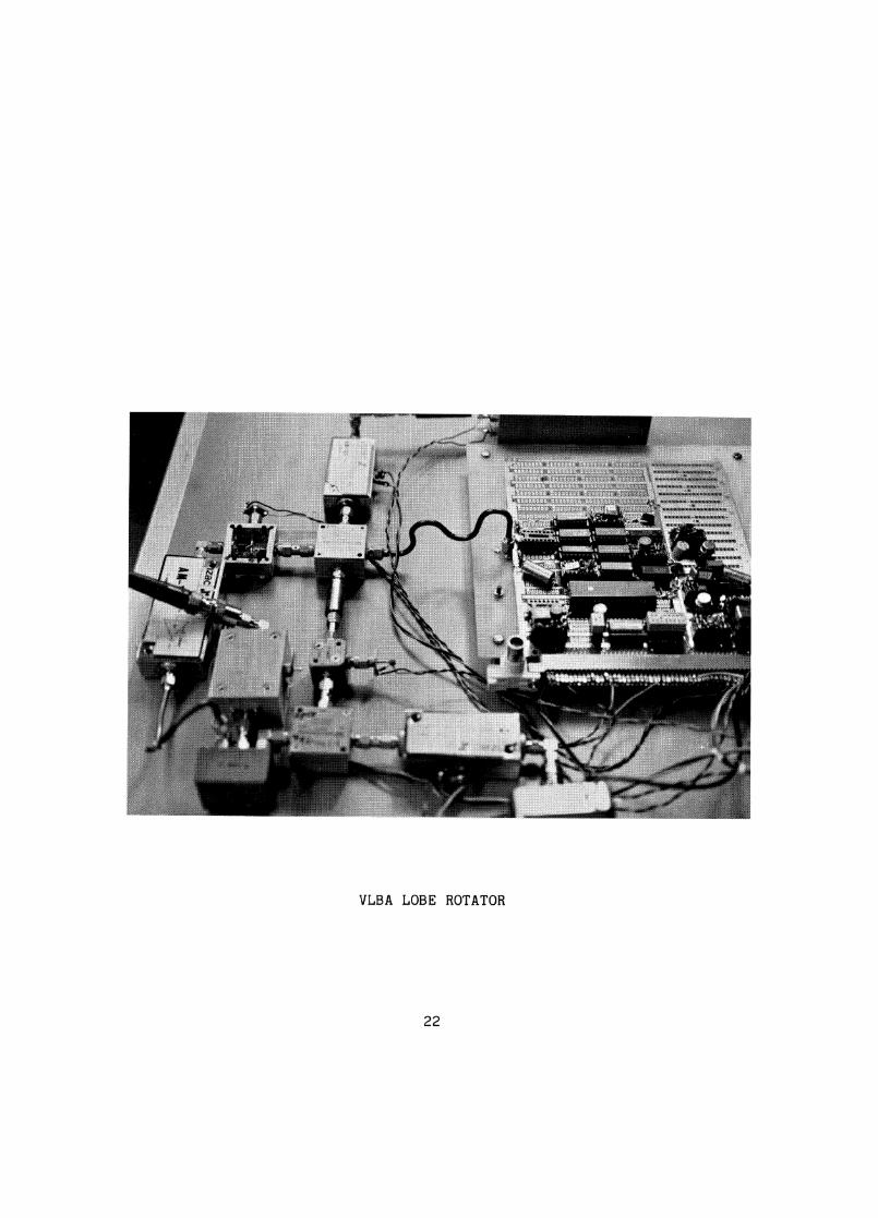
Photograph of VLBA Lobe Rotator . • •
•
•
•
• •
•
•
•
•
•
• . . • 22
• • •. • •
III. Detailed Design . . . . .• • • • • • • • • • • • • • • • •IV. Operating Instructions . . . . . • • • .• • .• • • • • • . .
y . .
• • . . 21. . . • • . • • . . .• • • • • • • • • • • • • • .
Photograph of VLBA Lobe Rotator . • • • • • • • . . • 22
• • • . 4Figure 3 VLBA Lobe Rotator Vendors • • • • • • • • • • • • • • . 5Figure 1
4 Clock Driver . . . . . . . . . . . . . . . . . . . . . 6
Figure 7 NCO's BlockFigure 6 NCO and DAC . . • • • • • • • • • • • • • • • • • • •
18.20
Figure 10 Long-Term Stability Test Configuration • • . • • • • .. .Figure 11 Long-Term Stability . . . • • • . . • • • • • • • .
Photograph of VLBA Lobe Rotator . • • • • • • • . . • 22
BREADBOARD 100 MHZ PHASE-SHIFTER FOR INTERFEROMETER LOBE-ROTATION
Joseph Greenberg
I. Introduction
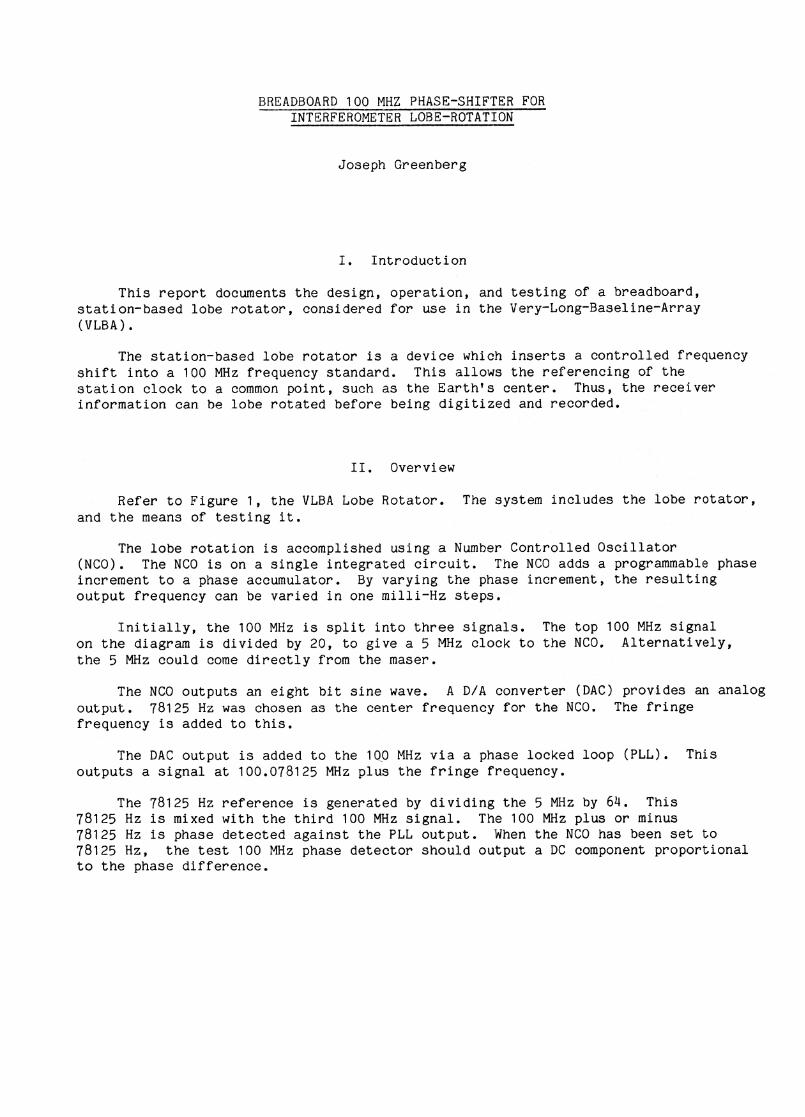
This report documents the design, operation, and testing of a breadboard,station-based lobe rotator, considered for use in the Very-Long-Baseline-Array(VLBA).
The station-based lobe rotator is a device which inserts a controlled frequencyshift into a 100 MHz frequency standard. This allows the referencing of thestation clock to a common point, such as the Earth's center. Thus, the receiverinformation can be lobe rotated before being digitized and recorded.
II. Overview
Refer to Figure 1, the VLBA Lobe Rotator. The system includes the lobe rotator,and the means of testing it.
The lobe rotation is accomplished using a Number Controlled Oscillator(NCO). The NCO is on a single integrated circuit. The NCO adds a programmable phaseincrement to a phase accumulator. By varying the phase increment, the resultingoutput frequency can be varied in one milli-Hz steps.
Initially, the 100 MHz is split into three signals. The top 100 MHz signalon the diagram is divided by 20, to give a 5 MHz clock to the NCO. Alternatively,the 5 MHz could come directly from the maser.
The NCO outputs an eight bit sine wave. A D/A converter (DAC) provides an analogoutput. 78125 Hz was chosen as the center frequency for the NCO. The fringefrequency is added to this.
The DAC output is added to the 100 MHz via a phase locked loop (PLL). Thisoutputs a signal at 100.078125 MHz plus the fringe frequency.
The 78125 Hz reference is generated by dividing the 5 MHz by 64. This78125 Hz is mixed with the third 100 MHz signal. The 100 MHz plus or minus78125 Hz is phase detected against the PLL output. When the NCO has been set to78125 Hz, the test 100 MHz phase detector should output a DC component proportionalto the phase difference.

78
J25 K
Hz
..111
1111
1111
1111
1111
0...1.1
•111111*
Z B
IT
DAC
76
.12
5K
11
2.1
-Y
VC
X00,0
7g
ia5
/1 •
1,Y
r
TE
CT
PD
ET
EC
roR
1001
411z
.±7
g.12
5klit
LP F
I-1E
. I
tv;
'
1 00til
ia
Li
78,1
25k
Pti
+N(>
4(a
,TH
6-5/
12/F
gF
ig. 1. V
LB
A L
obe R
ota
tor.

III. Detailed Design
This section describes in detail the modules of the system.
The system is constructed using a single NRAO E13800MI wire-wrap board. The100 MHz components are interconnected by OSM connectors.
Figure 2 shows the power levels. The Voltage Controlled Crystal Oscillator(VCXO) requires an attenuator followed by a buffer amplifier, since it has a highoutput impedance.
Figure 3 shows the vendor part numbers, at the block diagram level.
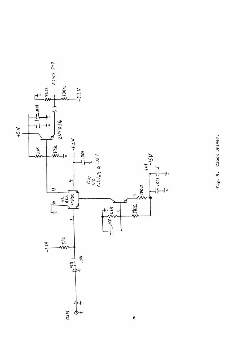
Figure 4 shows the clock driver for the ECL divider logic. The 100 MHz isinitially amplified by the RCA differential amplifier. 4C refers to the locationon the wire-wrap board. The emitter follower provides the necessary current. Threestrip lines distribute the clock to the three rows of logic. Each row is terminatedwith the equivalent of 50 Ohms. The NRAO Wire-wrap Board E13800MI contains thelayout for the clock driver.
Figure 5 shows the ECL divider circuitry. Synchronous counters are used tominimize phase instability. The flip-flops between stages resolve a race conditionin the timing. The 5 MHz output is converted to TTL levels by the 10125. The78125 Hz output goes through the voltage divider to provide a -7 dBm, 50 Ohmoutput. The 50 Ohms is based on a 7 Ohm ECL output impedance. The signal is ACcoupled to the mixer.
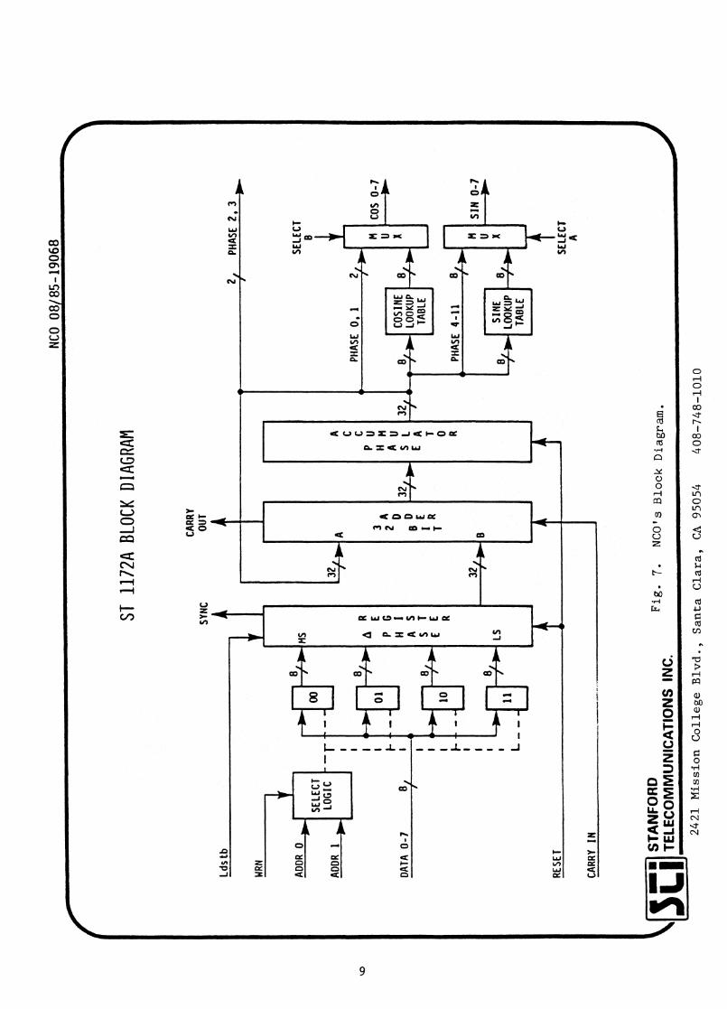
Figure 6 shows the NCO and DAC. The NCO is a Stanford Telecommunications ST-1172A, 40 pin chip. Figure 7 shows the NCO's block diagram. The 32 bit, phaseincrement is read in as four, eight bit numbers. The address is set in by a twoposition Dual In-line Package (DIP) switch on the board. The eight bit quartersof the phase increment are set in by an eight position DIP switch. The data setinto the DIP switches is strobed into memory by pressing the push button on theboard. The high to low transition activates the WRN line, which loads data intothe eight bit register specified by the address line. Also, the button activatesthe Ldstb line. The low to high transition loads the 8 bit registers into the 32bit, delta phase register. The carry in (CI) and reset lines are grounded.Select A being grounded causes a sine look-up table to be used for the output.Section IV, the operating instructions, provides details on the use of the NCO.
The eight bit sine wave goes to the National DAC0801LCJ DAC. This outputs ananalog current. Two ma. maximum output is specified by the current into pin 14.The OP-15 op amp serves as a current to voltage converter. The two ma. throughthe 1.5K feedback resistor gives three volts peak output. An adjustable one ma.is added into the summing junction to center the sine wave at zero volts. Thepush-pull emitter followers provide the current to drive the mixer. The crossoverdistortion is minimized by the op amp feedback. The 47 Ohm output resistorprovides the output impedance. The output voltage is divided by two when drivinga 50 Ohm load. Seven dBm is delivered to the mixer.
Figure 8 shows the mixer amplifier, loop phase detector, and loop filter.The DAC output can be seen entering from the top of the diagram. Mixed in is the
3

MH
z.
t6
q -78
,125
KH
z
I24
7 3.
1251
filz
+YF
7d&
v,! W
pm
.111*
17d
t2dB
VC
X0
100,
07V2
57”
tY
tn-
14..9
.d8m
I T
DAC
78.1
25R
ilztY
PH
AS
E I
NC
/RE
:PU
NT
LPF
Fig
. 2. V
LB
A L
obe R
ota
tor
Pow
er
Levels
.L7
7/6-
5/I 2
'86

PH
AS
E I
NC
RE
ME
NT
;FE
E.N
RA
YH
-522
fiti
NC
OS
BIT
DA
C78
.12.
51(1
12 tY
11 H
7 3
. /25
kHz
C Z
EP
1-2
fYF
mcF
SC
-3-1
3
F2
41
PM
MC
TA
X 5
P
tIT
OP
-Is
OP
-7
A?
11
0-1
13 A
Z A
l1-1
08
"IC
!OO
MH
MC
ZFO
C-0
-1I.-
78.1
:1510z zi
v-31
-11
AZ
AM
-105
VO
X.°
100.
07F/
25'r.
tYV
EC
TR
ON
C0
-23
3 V
FW'
LP
F
78, /
2 5
1, 04;
, 5
11
ST
-117
2AN
AT
ION
AL
DA
C 0
80
/ L
a
Mc
A Z
- A
nzac
Fig
. 3.
VL
BA
Lobe R
ota
tor
Vendo
rs.
. TH
G.
51/ 2
'8'6
45v
2N
5-3
3‘
RO
WS
5-
7
130.
st
—5.
2 V
5,/z
i-
rmis
tate
ro
Fig
. 4. C
lock D
river.

VC
C,
VE
E.
Flop
io Ge
PRO
r l C
LO
CH
DR
IVE
R
Fig
. 5. E
CL
Div
ider.
01
6 p
iozn
, 10
/03
/0
0/6
,10
olo
Vcc,-
- I,
lc, \
l€E
&N
o V
eE
r -S
.ZV
4u
u-O
P f
'Est
sTL
c

+5 v
To s
o, s
i
sx
4
C
CO
Ck
VO
D
/7
SE
LE
.CT
8FR
OM
2iv
IDER
51-/
/72A
NC
/0
CI
Ai5
8LS L
9
shil7 s
lA
16 '6
,15
shilf
st/V
3...s
/4/2
viti
l c/N
, RE
SE
T C
EL
E c
r A
\/$
s2..-7
. /3 i
z I
i16
— i i
2..I
L7
:12:
3 -- —
5.
__
... _
....._
.1P
i
CO
Fig
. 6
. N
CO
an
d D
AC
.
ID
3,4*
/0
2 3
71 )
. r\1
135 3
2-•
•-
wri
NA
5D
I11 A
bD
to 7
DA
TA
;TO
1,15
13M
S9
7...._ ....
....... —
gr\1
., fi
evs
9-1C
To 6
-ND
1 33 2
9 3
‘7..
I0
Ldst
b
WRN
ADDR
0
/00
ADDR
1
SELE
CTLO
GIC
--r
-
MS00
161 ■
Nrib
.
DATA
0-7
LS
SYNC
A
P
U m
AU
S (A 0
1274
0...
COS
0-7
Do-
NCO
08/8
5-1
9068
ST 1
172A
BLO
CK D
IAG
RAM
ACAR
RY
OU
T
1 2 A
SINE
4 --4-1
0. - LO
OKUP
TABL
E
PHAS
E 0,
PHAS
E 4-
11
1.1111
111111
111M
■■
=4
.11
11
1,
COSI
NELO
OKUP
TABL
E
2,PH
ASE
2,3
00-
SELE
CT
SIN
0-7 No
-
RESE
T
CARR
Y IN
SELE
CTA
3Ci S
TAN
FORD
TELE
COM
MU
NIC
ATIO
NS
INC.
Fig
. 7.
NCO
's B
lock
Dia
gra
m.
2421 M
issi
on C
olle
ge B
lvd., S
anta
Cla
ra, CA 9
5054
408-7
48-1
010

Os
445
LOO
PFI
LTER
78.i25" 1
1
FAO
Mpi
I X
ERQ2
3ç.
j g!
si.—
10 J
13,1
20
0) 3
447'
PIN
S
9109.
+IS
0K
3:94
0712 G
LAls
zo
.Cv
- ,kti
s cri
vp
7 76
/17r
)1A
7 TAK—
FRO
M P
AC
7d e
m
78.1
2_5 k
/ la
it7.5
1-15
71386 I
L2iM
1—zj
i F
445
;14
9/3
pil l
7
Ve.
-T
o V
C X
0 5
,17
,Gt
V P
907 7
0 P
i W
EW
I 37
- 4l<
?
34:
- S
i- 7
.c'
4,7 7. tt
J9. BL
UE
8E
AD
ofi
l
PIN
1
LOO
PPH
ASE.
DETECTO
R
(, 0
41-
g 0
k
•.14
13
MIX
ER
MIP
LIFJ
ER
n; ',
3
.9z
383
Fig
. 8.
Loop F
ilte
r.
- v
100
4. s
v5'451
t IsV
fin
cy
- V
riP
S r
3.*
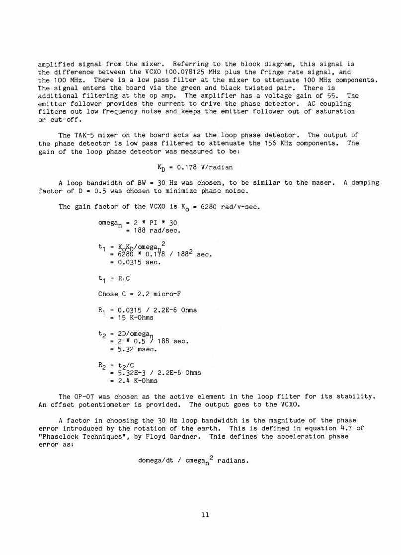
amplified signal from the mixer. Referring to the block diagram, this signal isthe difference between the VCXO 100.078125 MHz plus the fringe rate signal, andthe 100 MHz. There is a low pass filter at the mixer to attenuate 100 MHz components.The signal enters the board via the green and black twisted pair. There isadditional filtering at the op amp. The amplifier has a voltage gain of 55. Theemitter follower provides the current to drive the phase detector. AC couplingfilters out low frequency noise and keeps the emitter follower out of saturationor cut-off.
The TAK-5 mixer on the board acts as the loop phase detector. The output ofthe phase detector is low pass filtered to attenuate the 156 KHz components. Thegain of the loop phase detector was measured to be:
KD =
0.178 V/radian
A loop bandwidth of BW = 30 Hz was chosen, to be similar to the maser. A dampingfactor of D = 0.5 was chosen to minimize phase noise.
The gain factor of the VCXO is Ko = 6280 rad/v-sec.
omegan = 2 * PI * 30= 188 rad/sec.
ti1
= K0K0/omegan2= 6280 * 0.178 / 188 2 sec.= 0.0315 sec.
1 = R1C
Chose C = 2.2 micro-F
R1 = 0.0315 / 2.2E-6 Ohms
= 15 K-Ohms
t2 = 2D/omegan= 2 * 0.5 / 188 sec.= 5.32 msec.
R2 = t2/C= 5.32E-3 / 2.2E-6 Ohms= 2.4 K-Ohms
The OP-07 was chosen as the active element in the loop filter for its stability.An offset potentiometer is provided. The output goes to the VCXO.
A factor in choosing the 30 Hz loop bandwidth is the magnitude of the phaseerror introduced by the rotation of the earth. This is defined in equation 4.7 of"Phaselock Techniques", by Floyd Gardner. This defines the acceleration phaseerror as:
domega/dt / omegan2 radians.
1 1

To demonstrate the magnitude of the numbers involvded, consider a two-stationsystem.
Omega corresponds to the fringe rate in radians/second. Omegan is the loopbandwidth.
The fringe rate, v = D vrf /c cose de/dt Hz,
where: D = station separation of 6000 miles.vrf
= the rf frequency of 100 MHz.6 = the hour angle of the source.de/dt = the rotational rate of the earth.C = the velocity of light.
Differentiating:
dv/dt = -D vrf/c sine (de/dt)*(de/dt) Hz/sec.
The maximum values can be obtained by setting the sine or cosine equal toone. Substituting, the maximum, absolute values are:
= 235 Hz
dv/dt = 0.017 Hz/sec
These are within the actual VOX° parameters of plus or minus three KHz maximumdeviation and one KHz maximum modulation rate.
Substituting, the acceleration phase error equals:
0.017/ (30 2 * 2PI) = 3.00E-6 radians.
Converting the acceleration phase error to time:
3.00E-6 radians * 10,000 ps / 2PI radians = 0.0048 ps.
This compares well to the 0.60 ps phase error allowed for the maser, which willbe discussed in section V.A, Short Term Stability. Thus, the allowable accelerationphase error must be considered in defining the lower limit for the loop bandwidth.
IV. Operating Instructions
The system uses the following power supply voltages and currents:
+15 Volts - 75 ma.-15 Volts - 56 ma.-5.2 Volts - 0.63 Amp-20 Volts - 0.40 Amp+5 Volts - 50 ma.
A stable 100 MHz reference is required to test the system. In operation, themaser 100 MHz output would be used. A Greenray Model YH-522-45 Oscillator wasborrowed from Green Bank. 14 dBm of power was provided by 16 dB of attenuation,followed by 19 dB of amplification.
12

The phase increment must be initially entered into the NCO. This is accomplishedvia the DIP switches on the card. The two switch DIP enters the address. Theeight switch DIP enters one quarter of the phase increment at a time. The phaseincrement is added to the phase accumulator at the 5 MHz clock rate. The followingtable shows the switch settings and corresponding output frequencies.
TABLE I. NCO Output Frequencies in Hz
Off = Logic 1
AddressSwitch # Phase Switch #
1 2 1 2 3 4 5 6 7 8
0 0 78125 39063 195310 1 9766 4883 2441 1221 610 305 153 76.31 0 38.1 19.1 9.54 4.77 2.38 1.19 0.60 0.2981 1 0.149 0.075 0.037 0.019 0.009 0.005 0.0023 0.0012
To get a DC output from the test 100 MHz phase detector, a 78125 Hz output isrequired from the NCO. The 32 bits are entered by the following sequence:
Address Phase Switches00 00000100 Push Button to strobe data in01 00000000 Push Button10 00000000 Push Button11 00000000 Push Button
The PLL must acquire lock. Normally it will self-acquire lock within 2minutes. The process can be observed by monitoring the output of the test 100MHz phase detector. A sine wave will be observed. Initially it will slowlydecrease in frequency. The rate of change will accelerate as lock is approached.The final output frequency will be the absolute value of the frequency enteredvia the switches minus 78125 Hz. Lock can also be observed by watching the controlvoltage on the VCXO. The PLL offset potentiometer is set to cause the controlvoltage to integrate towards +15 volts on turn on Thus the loop drifts towardslock. If excessive time passes between turn-on and a frequency being enteredinto the switches, the loop amplifier might saturate. The system can be reset byturning the power off and on again. Alternatively, the loop offset potentiometeron 3B can be adjusted to pull the amplifier out of saturation towards lock. Readjustthe potentiometer for a positive offset later, with the loop out of lock. Thepotentiometer can not pull the loop out of lock, once lock has been acquired.
For maximum linearity, it is desirable to have the phase detector DC outputnear zero volts. To slew the output, enter a small frequency difference. Forexample: Assume 78125 Hz is initially set. Set the address to 11 and the phaseswitches to 00000100, then push the button. This gives a slew frequency of 0.005Hz. Set the phase switches to 00000001. When the test 100 MHz phase detectoroutput gets near zero volts, push the button. Then set the switches to 00000000.Push the button again when the output is nearest zero volts.
13

I .1.1•11.P.11.1.0
220 pH
0.033 pF 0.033 pF 51 Ohms
TODSA 1M-OHM
INPUT
FROMPD 50 OHMOUTPUT 220 pH
i 4 )
0.10 pF
The test 100 MHz phase detector can be made to output a sine wave of frequencyF by setting the switches to a frequency of 78125 Hz plus or minus F. For example:00 - 00000100, 01 - 00000100, 10 - 00000000, 11 - 00000000, gives 305 Hz. Toolarge a frequency step will temporarily knock the loop out of lock. The outputfrequency is limited by the three KHz deviation of the VCXO.
V. Stability Measurements
A. Short Term Stability
Short term stability was evaluated using the HP 3561A Dynamic Signal Analyzer(DSA). The test 100 MHz phase detector output is filtered by the 5 pole Butterworth,low-pass filter, shown below.
50 KHz Low-Pass Filter
The filter is necessary to attenuate the 100 MHz and 156 KHz components. Thedynamic range of the DSA is not great enough to include the 156 KHz signal leveland the expected level of phase noise.
The output of the filter goes to the DSA. The input circuit ground switchis put in the float position. This cuts down 60 Hz pick-up by eliminating theground loop.
The maser is specified, in specification A53308N001. The maser phase fluctuationshould be less than 0.6 ps rms over the frequency range 1 Hz to 1 MHz. To measurethe lobe rotator's phase fluctuation, the NCO output is set to 78125 Hz. Thetest 100 MHz phase detector then outputs a dc component. To have the phasedetector in its linear region, and to keep the DSA from over-loading, the dccomponent is set near zero volts. The dc component can be slewed by turning onand off small frequency increments.
Figure 9 shows the outputs obtained from the DSA. The y axes show volt2/Hz.On the DSA, auto range was turned off. A single auto-range gave a range of-41 dBV. A 50 Ohm load on the input of the DSA then gave a noise level of -158dBV. This is below the phase noise values to be measured.
Figure 9A shows the phase noise from 0 to 200 Hz, on a linear scale. Note thereduction in phase noise in the initial 30 Hz, due to the PLL bandwidth. A
14
1 A:MOTHHA 2 :: ri
RANGE: -41 c!BV P141.1 ED• / •1-1 RNS:RR
A. 0 - 200 Hz - Linear Scale
RANGE: -41 dBV .STATUA7=: PAUSED
B. 0 - 2 KHz - Log Scale
..... • . . . . . . .. . . . . . . .
• • •,h
.... ., 0t(N)•2!START: 0 HzIX: 29.5 Hz
BW: 1.9097 Hz'.1 1 : 46.34 P 2
5.623P(Y)-2/DIV
-STOP: 200 Hz
11.4
•• I
•
RMS;100'
STOP:BW: 19.097 HzY:-55.27 dB<V)
11
1
2 000 Hz
-80dB(V)
10ciE
/DIV
-160 I_START: 0 HzX: 5 Hz
10dB
sDIV
START: 0 Hz BW: 954.85 Hz OF: 100 c. A0 HzX; 0 Hz 09 dB<V>
C. 0 - i00 KHz - Log Scale
15
Fig. 9. Short-Term Stability.
. ,-80
dS(V)
RANGE: -41A:MATH • B14
STATUS: PAUSEDRMS:100
I •
I .

strong 60 Hz component can be seen. Broadening the loop bandwidth to 300 Hz,instead of 30 Hz, eliminated the 60 Hz phase peak.
The phase fluctuation can be calculated by integrating the graph with respectto frequency. On Figure 9A, each block is 5.623E-12 V 2 /Hz by 20 Hz. This givesan area of 1.12E-10 V2 /block. 15 blocks are counted under the curve, temporarilyignoring the 60 Hz components. 1.12E-10 V 2 /block * 15 blocks gives 1.69E-9 V2.Taking the square root gives V Rms = 4.11E-5 V. It is desired to express this asan rms time variation. The test 100 MHz phase detector gain, with the 50 KHzfilter attached, measures KD = 0.25 V/radian.
tRMS = VRMS * (radian/0.25 V) * (1E4 ps/2PI radians)
tRMS = VRMS * 6366 ps/V
For the phase noise 0 to 200 Hz, less the 60 Hz components:
tRMS : 0
4:126
* 6366 ps/V
Figure 9B shows the same signal on a log scale with a frequency range of 0to 2 KHz. The three main components of the phase noise can be seen. They are:
1. The 1/f noise, as was measured with figure 9A.
2. The 60 Hz components.
3. The flat, broad-band noise at -135 dBV.
The phase noise due to the 60 Hz components can be calculated as follows. Usingthe display of figure 9B, the peak values were read on the DSA as follows:
60 Hz - 348.7E-12 V2/Hz
120 Hz - 3.5E-12 V2/Hz
180 Hz - 4.0E-12 V2/Hz
240 Hz - 0.9E-12 V2/Hz
The phase fluctuation can be obtained by integration. Each peak is assumedto be a triangle with a base width of the measurement band-width (19.1 Hz). Thusthe integration yields:
(348.7 + 3.5 + 4•0 + 0.9)E-12 V2 /Hz * 19.1 Hz / 2 = 3.41E-9 V2
tRMS = SQRT(3.41E-9 V2) * 6366 ps/V
= 0.37 Ps.
Figure 9C shows the 0 to 100 KHz spectrum of the same signal. The 78.125 KHzsignal is due to some of the 100 MHz carrier being present from the previous
16

mixer. The 100 MHz then mixes with the 100.078125 MHz to give the 78.125 KHz.The 39.0625 KHz comes with the 78.125 KHz signal from the divide by 64. The nextdivider stage causes the distortion. The peaks at 21 KHz, 56 KHz, and 100 KHzare spurious signals from the DSA. They disappear when the DSA, input circuitground switch is put in the chassis position (i.e. The input ground is notfloating). Since these are not corruptions of the VOX° output, they can beignored in computing the phase fluctuation of the VCX°. The dc spike can beignored, since it is the constant phase offset. The flat portion represents thebroad-band noise level of -135 dBV. The falling off, starting at 30 KHz, coincideswith the 50 KHz filter curve. The rms phase fluctuation can be calculated byintegrating with respect to frequency. It is assumed that all significant phasenoise is less than 100 KHz. 100 KHz is also the upper limit of the DSA. -135dBV equals 3.16E-14 V 2 /Hz. Multiplying by 100,000 Hz gives 3.16E-9 V 2 . Thisgives a phase fluctuation of:
tRMS SQRT(3.16E-9) * 6366 ps/V= 0.36 ps.
Combining the 1/f and broad-band noise phase fluctuations gives:
tRMS SQRT(0.26 2 +0.36 2 ) ps= 0.44 ps.
Combining in the 60 Hz phase noise yields:
tRMS - SQRT(0.44 2 + 0.372)-= 0.57 ps.
However, the 60 Hz noise should be easily attenuated by building the systemin a shielded enclosure, as opposed to the breadboard's open construction.
These all meet the maser specification of 0.6 ps rms. An improvement of a factorof three would be needed in a final system.
With the DSA in the 0 to 2 KHz range, the lobe rotator was set to output305 Hz. An auto-range was performed to the -15dBV range. The 305 Hz carrier hada peak value of -27.4 dBV/Hz. The noise floor was down 90 dB, due to the dynamicrange of the DSA. However, the carrier value could be compared to the noise fromfigure 9B, to give the actual dB below the carrier. Figure 9B shows the phasenoise without a large carrier or DC component present to saturate the DSA. Thefollowing values were calculated:
100 Hz away 88 dBc/Hz
200 Hz away 96 dBc/Hz
1000 Hz away 106 dBc/Hz
2000 Hz away 107 dBc/Hz
These values coincide well with the specification of the VCXO.
17

_ _ > Apple II+Computer
TO DSAFROM PD
0.01 pF 1 pF
If the 100 MHz signal was multiplied to 100 GHz, the carrier to noise levelswould deteriorate by 60 dB. Thus, it is evident that some noise improvement ofthe lobe rotator or further clean-up in a narrow-band PLL is needed. A 10 dblower phase noise VCXO is available which could improve the lobe rotator phasenoise. This is further discussed in Section VI, Possible System Improvements.
B. Long Term Stability
The long term stability was analyzed using the Frequency Standard Test Program,which is described in Electronics Division Internal Report No. 232 by S. Weinreb.
Fig. 10. Long Term Stability Test Configuration
LobeRotatorTest100 MHzPhaseDetector
Low -->Pass
Filter / X100I. Amplifier
Temperature - - - - - Probe
5 KHz Low Pass Filter Details
10 pH 1 mH
Figure 10 shows the long term stability test configuration. The test 100 MHzphase detector outputs to a two stage low pass filter. The 1K resistor providesa suitable load. The first stage filters out components 100 MHz and above. Thesecond stage filters out 5 KHz and above. The output of the filter goes to thebattery powered NRAO LOG AMP. The DB/DIV switch is in the LIN position forlinear operation. The +/- switch is in the + position. The CAL/3 DB switch isin the CAL position. This provides a low noise linear amplifier with a gain of100. The amplifier outputs to the ADIOS A/D A IN port. A temperature probe isconnected to the B channel, as described in Internal Report No. 232. The temperatureprobe is taped to the NRAO LOG AMP. The ADIOS A switches are set to +- 1 V. TheB switches are set to + 10 V. The Apple II+ computer runs the program FST86. Thistakes the data and computes the Allan variances.
18

The following parameters were fed to the program:
1. Phase detector full scale = 30 ps.
This is calculated from the 100 MHz, test phase detector gain, K D =0.535 volts/radian. Note this is higher than the value used in the shortterm stability calculations. This is due to less loading by the LPF.
0.535 volts/radian * 100 gain * 2*PI radians / 10000 ps = 1 volt / 30. ps.
2. A perfect reference is assumed.
Figure 11 shows the long term stability outputs from the program. A continuousseries of 13000 second runs was set up to run over night.
Figure 11A shows the last 13000 second run. The squares show the 1 second Allanvariances. The crosses show the frequency drift. The line reflects the roomtemperature variation. The cycling of the air conditioner can be clearly seen.There is a peak to peak variation of 0.6 degrees C., and a period of 1800 seconds.The period was longer for night 13000 second runs. The temperature variation hasonly a minor effect on the lobe rotator operation.
Figure 11B shows the lobe rotator Allan variances for the 14.5 hours ofdata The maser specification is shown on the diagram. The lobe rotator meets thecriteria set forth in VLBA Acquisition Memo #60, by Alan Rogers. That criteriais that the Allan variance of the phase error in the rotation should be less thanone third the maser Allan variance specification. The hump in the data around1000 seconds can be attributed to the temperature cycling.
To determine the stability of the test 100 MHz phase detector, 9dBm at 100 MHzwas fed directly into the L and R ports of the phase detector. Since this is 5dB down from the power levels used in the lobe rotator, the full scale phasedetector value of 30 ps was divided by 10E(-5/20) to give 53 ps. The Allan variancecan be seen in Figure 11C. It is about an order of magnitude better than thetotal lobe rotator.
Figure 11D shows the stability of the X100 amplifier with a 50 Ohm load on theinput. A 30 Ps full scale value was used This exceeds the stability of thephase detector as expected.
VI. Possible System Improvements
The breadboard system uses an open construction method. The system could beenclosed in a well shielded cabinet to reduce 60 Hz pick-up.
Currently, the 100 MHz components are interconnected by OSM connectors. Aprototype system could have the 100 MHz components mounted on a PC board, inter-connected by microstrips. This would reduce component cost and module size.
19

-11LOG
:"..;; I GMAbtC
AWE
11001 FREQ
DRIFT*E-12
-11LOG
SIGMAUSTAU
-14 ,Vralkal-15
-100 -1613g013
-14TEMPSPANSc
100 1000 10000 SEC
11111111111111111111111111111111
11111111111111111111111111111111111111111110111111:11111111111111111111111
IA 1 CA A 1 174 Ci il 1 ta Ct A ki ',..;
-11LQG
SIWIAUtnu
-14
-15
_11
LOGS I MA
USTAU
-14
-15
-16
111111111111111111111111111111111111111111111
111.11111111111RD MIMI
Fig. 11. Long-Term Stability.
NRAO Maser Spec.
IIIIIIIIIIIWAIIIII111111111111
low.„111111111111""1911111AM. —
10 :.100 I oori 0 kirin
A. Fringe Rotator - B. Fringe Rotator -Last 13,000 Second Batch Allan Variance Values
C. Test Phase Detector - XAO Amplifier -Allan Variance Values itlan Variance Values
20
The mixer amplifier of figure 8 would be better mounted near the mixer, to reducenoise pickup.
The system is susceptible to microphonics, so a low vibration environment isdesirable.
Having the system in a temperature controlled environment would enhance longterm stability.
It would be desirable for a prototype system to contain circuitry to aid thePLL in acquiring lock. This could be achieved by alternately slewing the VCXO controlvoltage up and down. A lock detector could shut off the slewing mechanism, oncelock is attained. Otherwise, continued slewing would stress the loop and cause aphase offset.
The phase increment could be entered via computer rather than by hand.
If it is desired that the output be at 100 MHz plus the fringe frequency, asecond PLL could be added. This PLL could subtract the 78125 Hz reference fromthe current system output. This second PLL would add some phase instability.
Refer back to Figure 1. The lobe rotator output from the directional couplerhad sidebands plus and minus 78125 Hz from the carrier. These were down 70 dB belowthe carrier. They were not present on the output of the VOX°. They are due tosignals returning from the mixer into the 10 dB port of the directional coupler.These signals could be greatly attenuated by using a buffer amplifier from thedirectional coupler to the mixer.
A lower phase-noise VCXO could be used to improve the short term stability.Ed Selig at Vectron (203-853-4433) was contacted. The Vectron CO-233VFWT ($315)is the current VCXO. For $50 additional, they could reduce the phase noise10 dB.
VII. Conclusion
This lobe rotator would be a viable way to implement lobe rotation by frequencyoffsetting the reference signal.
21
firtaler\
ot; vto,„ Z*".,
t,;‘
VLBA LOBE ROTATOR
22