Embed Size (px)
Citation preview
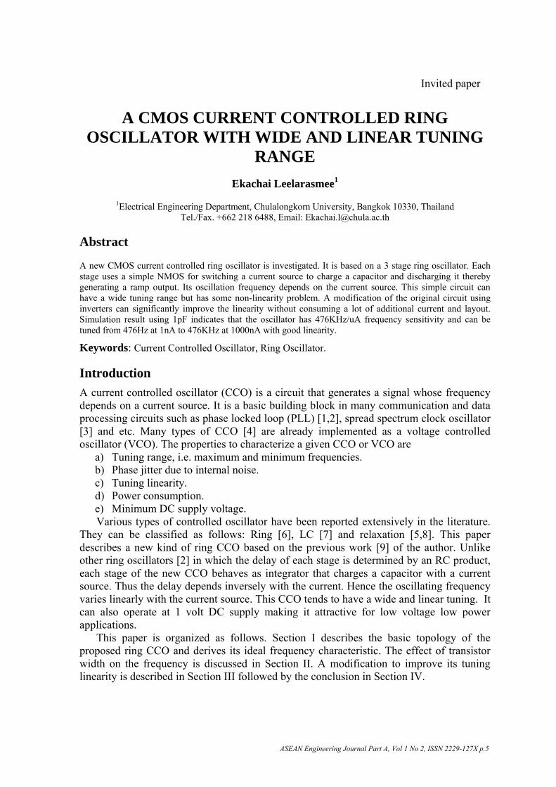
A CMOS CURRENT CONTROLLED RING OSCILLATOR WITH WIDE AND LINEAR TUNING
RANGE Ekachai Leelarasmee1
1Electrical Engineering Department, Chulalongkorn University, Bangkok 10330, Thailand Tel./Fax. +662 218 6488, Email: [email protected]
Abstract
A new CMOS current controlled ring oscillator is investigated. It is based on a 3 stage ring oscillator. Each stage uses a simple NMOS for switching a current source to charge a capacitor and discharging it thereby generating a ramp output. Its oscillation frequency depends on the current source. This simple circuit can have a wide tuning range but has some non-linearity problem. A modification of the original circuit using inverters can significantly improve the linearity without consuming a lot of additional current and layout. Simulation result using 1pF indicates that the oscillator has 476KHz/uA frequency sensitivity and can be tuned from 476Hz at 1nA to 476KHz at 1000nA with good linearity. Keywords: Current Controlled Oscillator, Ring Oscillator.
Introduction A current controlled oscillator (CCO) is a circuit that generates a signal whose frequency depends on a current source. It is a basic building block in many communication and data processing circuits such as phase locked loop (PLL) [1,2], spread spectrum clock oscillator [3] and etc. Many types of CCO [4] are already implemented as a voltage controlled oscillator (VCO). The properties to characterize a given CCO or VCO are
a) Tuning range, i.e. maximum and minimum frequencies. b) Phase jitter due to internal noise. c) Tuning linearity. d) Power consumption. e) Minimum DC supply voltage. Various types of controlled oscillator have been reported extensively in the literature.
They can be classified as follows: Ring [6], LC [7] and relaxation [5,8]. This paper describes a new kind of ring CCO based on the previous work [9] of the author. Unlike other ring oscillators [2] in which the delay of each stage is determined by an RC product, each stage of the new CCO behaves as integrator that charges a capacitor with a current source. Thus the delay depends inversely with the current. Hence the oscillating frequency varies linearly with the current source. This CCO tends to have a wide and linear tuning. It can also operate at 1 volt DC supply making it attractive for low voltage low power applications.
This paper is organized as follows. Section I describes the basic topology of the proposed ring CCO and derives its ideal frequency characteristic. The effect of transistor width on the frequency is discussed in Section II. A modification to improve its tuning linearity is described in Section III followed by the conclusion in Section IV.
Invited paper
ASEAN Engineering Journal Part A, Vol 1 No 2, ISSN 2229-127X p.5
Basic principle of the proposed ring CCO A typical ring CCO consists of an odd number of inverting stages connected as shown in Figure1. where the number of stage is 3. The period of oscillation generally depends linearly upon the delay of each stage which must be tunable in order to obtain a controlled oscillator.
2iv1iv 3iv01v 03v02v
Figure 1. Topology of a 3 stage ring oscillator
Each stage can be implemented using various circuits [4], many of which use the RC product to create its delay. Our proposed circuit is shown in Figure. 2. Its delay is due to the current I charging the capacitor C where an NMOS is used for discharging it.
ov
c
I
VDD
Miv
Figure 2. The inverting stage in the proposed CCO
Assuming that the NMOS operates as an ideal switch, i.e. the drain-source becomes short circuit when the gate voltage exceeds its threshold voltage THV , the waveforms of all output are shown in Figure 3. We can briefly describe the circuit operation as follows. While the NMOS of the first stage is OFF, the current I charges the capacitor C and its drain output starts to ramp at a slope of I / C . When this voltage reaches THV , the second stage turns ON and completely discharges its capacitor, turning OFF the third stage and so on. Figure 2 also shows that the start-up time of this CCO is less than one period T.
To find the frequency of oscillation, we note that during a period T each stage takes only T/3 to ramp up from zero to THV . Therefore
THI TVC 3
= × or TH
1 IfT 3CV
= =
ASEAN Engineering Journal Part A, Vol 1 No 2, ISSN 2229-127X p.6

Figure 3. Waveforms of the proposed CCO in the ideal case where THI 35nA, C 1pF, V 0.7V= = =
Thus the frequency varies linearly with I and the sensitivity is given by
TH
f 1SI 3CV
Δ= =Δ
For example, if I 35nA,= C 1pF,= and THV 0.7V= we have
f 16.7KHz= with KHzS 476
Aμ=
The formula also indicates the potential of wide tuning range with constant current consumption 3I . As the peak of the ramp is equal to TH2V , the minimum DC supply DDV to maintain NMOS in saturation mode is given by
DD I THV (min) V 2V= + where IV is the minimum operating voltage of the current source. Therefore this oscillator can operate at a DC supply less than 1.8V.
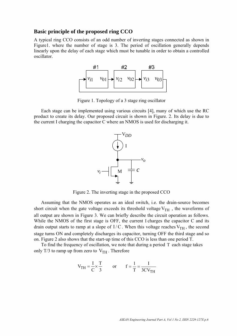
Non-ideal effect due to width of NMOS transistor To behave as an ideal switch, the NMOS must be able to sink an infinite current immediately. This does not occur since the NMOS can only have a finite width W. So, the drain output actually takes some time to drop and its low level is also slightly above zero. Moreover, since the gate input is ramping up, the NMOS will turn on gradually allowing the output to continue increasing before starting to drop. This results in delaying the switching time of the next stage as shown in Figure. 4.
ASEAN Engineering Journal Part A, Vol 1 No 2, ISSN 2229-127X p.7
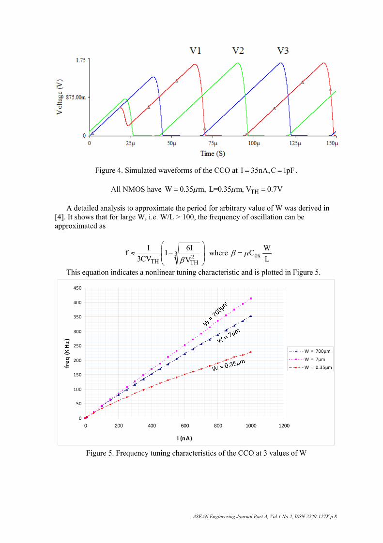
Figure 4. Simulated waveforms of the CCO at I 35nA,C 1pF= = .
All NMOS have THW 0.35 m, L=0.35 m, V 0.7Vμ μ= =
A detailed analysis to approximate the period for arbitrary value of W was derived in [4]. It shows that for large W, i.e. W/L > 100, the frequency of oscillation can be approximated as
3 2TH TH
I 6If 13CV Vβ
⎛ ⎞⎜ ⎟≈ −⎜ ⎟⎝ ⎠
where oxWCL
β μ=
This equation indicates a nonlinear tuning characteristic and is plotted in Figure 5.
0
50
100
150
200
250
300
350
400
450
0 200 400 600 800 1000 1200
I (nA)
freq
(KHz)
W = 700μm
W = 7μm
W = 0.35μm
Figure 5. Frequency tuning characteristics of the CCO at 3 values of W
ASEAN Engineering Journal Part A, Vol 1 No 2, ISSN 2229-127X p.8
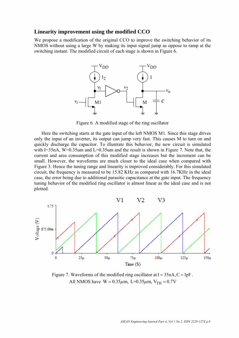
Linearity improvement using the modified CCO We propose a modification of the original CCO to improve the switching behavior of its NMOS without using a large W by making its input signal jump as oppose to ramp at the switching instant. The modified circuit of each stage is shown in Figure 6.
ov
iv c
2v1v
I2I
VDDVDD
M1 M
Figure 6. A modified stage of the ring oscillator
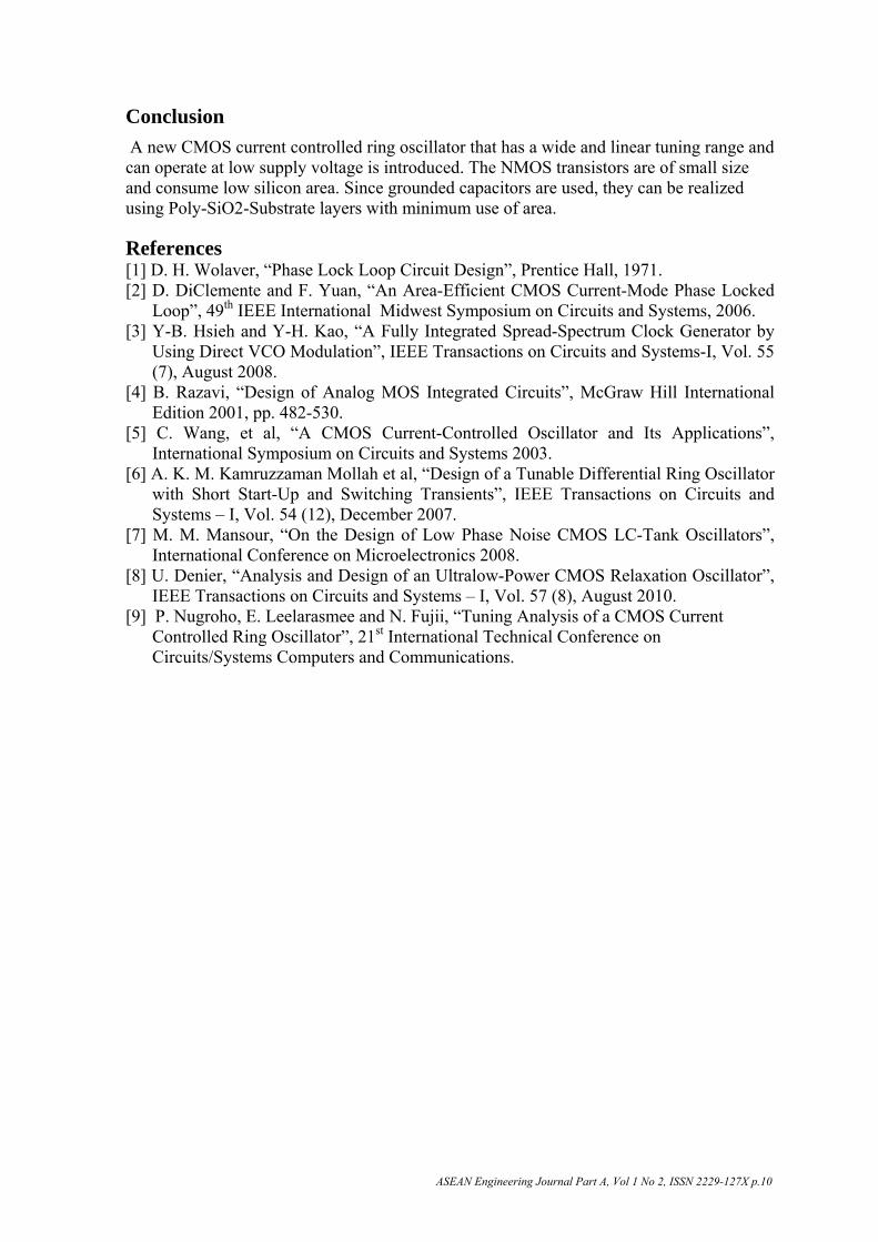
Here the switching starts at the gate input of the left NMOS M1. Since this stage drives only the input of an inverter, its output can jump very fast. This causes M to turn on and quickly discharge the capacitor. To illustrate this behavior, the new circuit is simulated with I=35nA, W=0.35um and L=0.35um and the result is shown in Figure 7. Note that, the current and area consumption of this modified stage increases but the increment can be small. However, the waveforms are much closer to the ideal case when compared with Figure 3. Hence the tuning range and linearity is improved considerably. For this simulated circuit, the frequency is measured to be 15.82 KHz as compared with 16.7KHz in the ideal case, the error being due to additional parasitic capacitance at the gate input. The frequency tuning behavior of the modified ring oscillator is almost linear as the ideal case and is not plotted.
Figure 7. Waveforms of the modified ring oscillator at I 35nA,C 1pF= = . All NMOS have THW 0.35 m, L=0.35 m, V 0.7Vμ μ= =
ASEAN Engineering Journal Part A, Vol 1 No 2, ISSN 2229-127X p.9
Conclusion A new CMOS current controlled ring oscillator that has a wide and linear tuning range and can operate at low supply voltage is introduced. The NMOS transistors are of small size and consume low silicon area. Since grounded capacitors are used, they can be realized using Poly-SiO2-Substrate layers with minimum use of area.
References [1] D. H. Wolaver, “Phase Lock Loop Circuit Design”, Prentice Hall, 1971. [2] D. DiClemente and F. Yuan, “An Area-Efficient CMOS Current-Mode Phase Locked
Loop”, 49th IEEE International Midwest Symposium on Circuits and Systems, 2006. [3] Y-B. Hsieh and Y-H. Kao, “A Fully Integrated Spread-Spectrum Clock Generator by
Using Direct VCO Modulation”, IEEE Transactions on Circuits and Systems-I, Vol. 55 (7), August 2008.
[4] B. Razavi, “Design of Analog MOS Integrated Circuits”, McGraw Hill International Edition 2001, pp. 482-530.
[5] C. Wang, et al, “A CMOS Current-Controlled Oscillator and Its Applications”, International Symposium on Circuits and Systems 2003.
[6] A. K. M. Kamruzzaman Mollah et al, “Design of a Tunable Differential Ring Oscillator with Short Start-Up and Switching Transients”, IEEE Transactions on Circuits and Systems – I, Vol. 54 (12), December 2007.
[7] M. M. Mansour, “On the Design of Low Phase Noise CMOS LC-Tank Oscillators”, International Conference on Microelectronics 2008.
[8] U. Denier, “Analysis and Design of an Ultralow-Power CMOS Relaxation Oscillator”, IEEE Transactions on Circuits and Systems – I, Vol. 57 (8), August 2010.
[9] P. Nugroho, E. Leelarasmee and N. Fujii, “Tuning Analysis of a CMOS Current Controlled Ring Oscillator”, 21st International Technical Conference on Circuits/Systems Computers and Communications.
ASEAN Engineering Journal Part A, Vol 1 No 2, ISSN 2229-127X p.10