Embed Size (px)
Citation preview
CMOS Fractal Oscillator Design for Frequency-Shift
Keying Modulation Using Multiplexers
Sung-jin Kim,1 Won-yong Choi,
1 Kang-in Heo,
1 and Gyu Moon
1,2
1Department of Electronic Engineering, Hallym University 1
Hallymdaehak-gil, Chuncheon, Gangwon-do, KOREA
2Research Institute of Informatic and Electronic Engineering, Hallym University 1
Hallymdaehak-gil, Chuncheon, Gangwon-do, KOREA
Corresponding Author: [email protected]
Abstract. A new version of the well-known FSK (Frequency-Shift Keying)
modulation technique for telecommunication system was proposed and verified.
A simple form of ring oscillator with three inverters was adopted for the basic
frequency generator. The frequency shift was realized using a ring oscillator
composed of nine inverters. CMOS multiplexers were used to select one of two
different oscillators, i.e., to shift between two different frequencies. Simulations
were performed for the verification.
Keywords: Multiplexers, CMOS Fractal Oscillator, Frequency Shift Keying,
GHz Oscillator.
1 Introduction
A novel type of Frequency-Shift Keying (FSK) modulation technique that uses a
CMOS oscillator with multiplexers is introduced.
The CMOS oscillator in its fractal structure generates and distributes a gigahertz
(GHz)-level oscillation signal [1-3].
This fractal oscillator supplies clock signals for today‟s widely used high-speed
digital circuits, and has a steady oscillation property with minimum clock skews. The
fractal oscillator circuit is much simpler and easier to implement than the well-known
Phase Locked Loop (PLL) circuit [2-4].
The FSK modulation is achieved by multiplexers, by choosing a different path in
the CMOS fractal oscillator. One of the two different frequencies, f1 and f2, is
selected by the multiplexer switch.
The multiplexer is composed of three two-input NAND gates and one inverter.
Only one fractal cell has a different path with multiplexers, generating a global
frequency change of f1+△f = f2. Then the multiplexer selection will yield the FSK
modulation in the simplest way [5-6].
Advanced Science and Technology Letters Vol.106 (Information Technology and Computer Science 2015), pp.27-32
http://dx.doi.org/10.14257/astl.2015.106.07
ISSN: 2287-1233 ASTL Copyright © 2015 SERSC
2 GHz-level Clock Distribution Technique with a CMOS
Fractal Oscillator
2.1 CMOS fractal oscillator structure
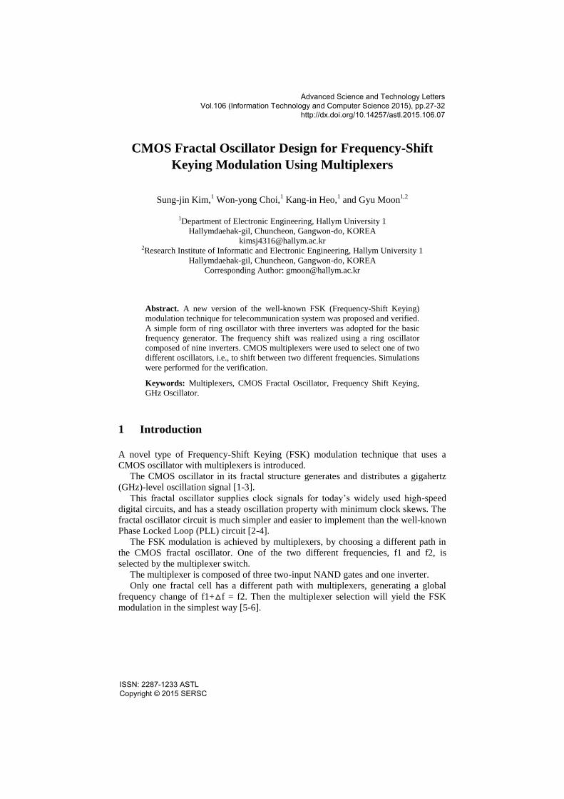
Fig. 1 shows the structure of the CMOS fractal oscillator. Although 108 inverters are
shown, they can be spread out fractal.
As shown in the figure, each fractal cell consists of three inverting elements, which
configure a ring oscillator. Each inverting element is shared with its three adjacent
cells. Thus, this oscillator can spread out infinitely in the 2D or 3D fractal mode.
Each inverting element, which in this paper is a simple CMOS inverter, has a ⅔π
phase difference because three inverters will consume a complete cycle (2 π) [1 and
3].
Given external power (3 V in this study), each fractal cell will oscillate; and due to
its structure, each node in Fig. 1 will generate the same frequency oscillating signal.
Note that even with a local change in a few nodes, the change will be instantly
„averaged‟ through the fractal networks, and the frequency of each node will stay the
same, within a minimum clock skew [1 and 3].
Fig. 1. A CMOS fractal oscillator with 108 inverters.
2.2 Fractal oscillator FSK modulation
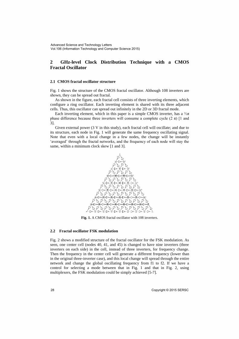
Fig. 2 shows a modified structure of the fractal oscillator for the FSK modulation. As
seen, one center cell (nodes 40, 41, and 45) is changed to have nine inverters (three
inverters on each side) in the cell, instead of three inverters, for frequency change.
Then the frequency in the center cell will generate a different frequency (lower than
in the original three-inverter case), and this local change will spread through the entire
network and change the global oscillating frequency from f1 to f2. If we have a
control for selecting a mode between that in Fig. 1 and that in Fig. 2, using
multiplexers, the FSK modulation could be simply achieved [5-7].
Advanced Science and Technology Letters Vol.106 (Information Technology and Computer Science 2015)
28 Copyright © 2015 SERSC
Fig. 2. 2.1. FSK modulation CMOS oscillator with a local change at the center cell
Fig. 3. Diagram of the FSK modulation scheme with a multiplexer
Fig. 3 shows a diagram of the FSK modulation scheme with a multiplexer. The
SEL control signal selects one of the two different paths with two different
frequencies, f1 (upper) and f2 (lower), which will serve as the two FSK modulation
signals.
Fig. 4 shows a logic diagram for a 2-to-1 multiplexer.
Using three NAND gates and one inverter, one of the frequencies will be selected:
f1 when SEL = 0, or f2 when SEL = 1.
f1
f2
SEL OUT
MUX
Fig. 4. 2-to-1 Multiplexer logic diagram.
3 SPICE Simulation Results for the FSK Modulation
Combining Figs. 1, 2, and 3, SPICE simulations were performed. The results are
shown in Fig. 5. The FSK frequency change is clearly shown in the bottom graph with
the corresponding SEL (FSK0 and FSK1) changes. A power supply of 3 volts, a
Advanced Science and Technology Letters Vol.106 (Information Technology and Computer Science 2015)
Copyright © 2015 SERSC 29
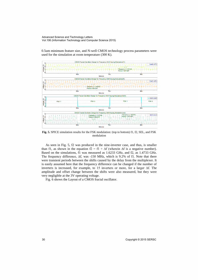
0.5um minimum feature size, and N-well CMOS technology process parameters were
used for the simulation at room temperature (300 K).
Fig. 5. SPICE simulation results for the FSK modulation: (top to bottom) f1, f2, SEL, and FSK
modulation
As seen in Fig. 5, f2 was produced in the nine-inverter case, and thus, is smaller
than f1, as shown in the equation f2 = f1 + ∆f (wherein ∆f is a negative number).
Based on the simulations, f1 was measured as 1.6233 GHz, and f2, as 1.4733 GHz.
The frequency difference, ∆f, was -150 MHz, which is 9.2% of f1. Note that there
were transient periods between the shifts caused by the delay from the multiplexer. It
is easily assumed here that the frequency difference can be changed if the number of
inverters is increased, for example, to 15 inverters or more, for a larger ∆f. The
amplitude and offset change between the shifts were also measured, but they were
very negligible at the 3V operating voltage.
Fig. 6 shows the Layout of a CMOS fractal oscillator.
Advanced Science and Technology Letters Vol.106 (Information Technology and Computer Science 2015)
30 Copyright © 2015 SERSC
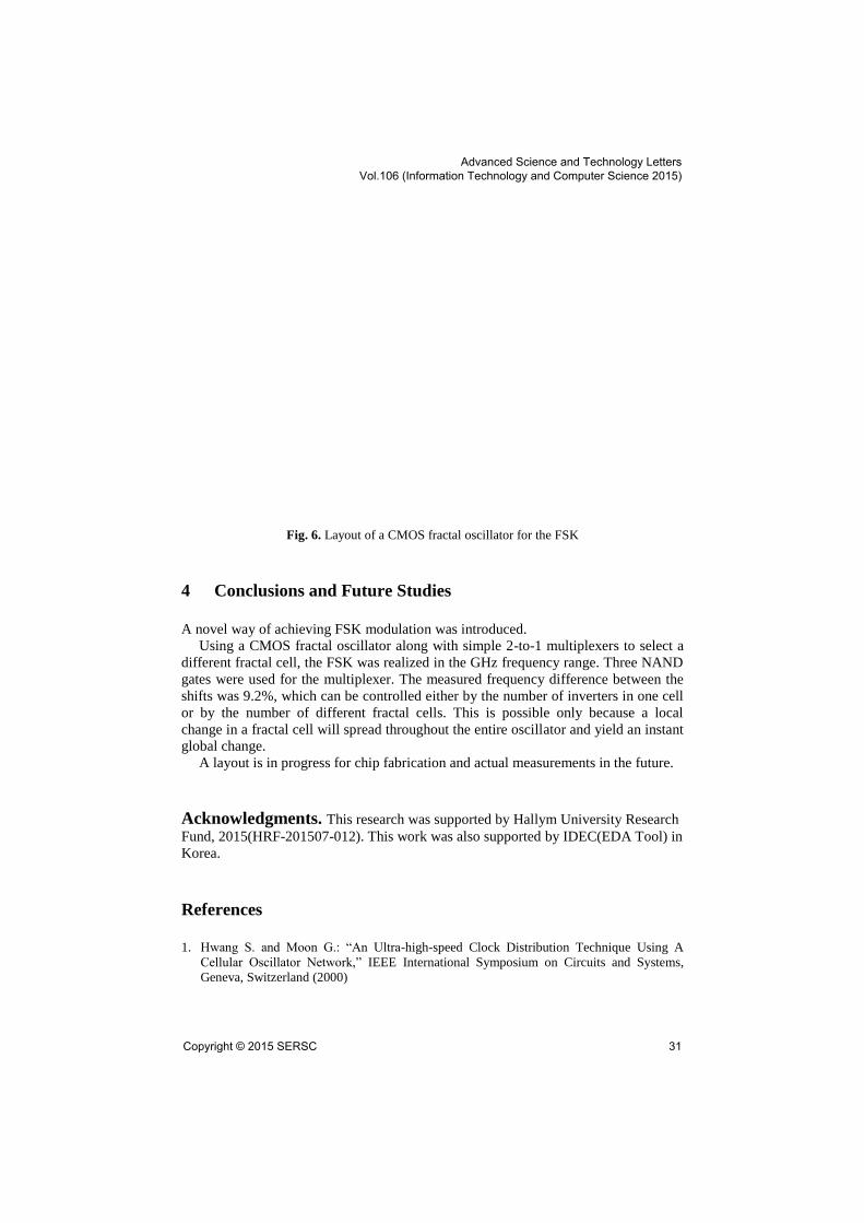
Fig. 6. Layout of a CMOS fractal oscillator for the FSK
4 Conclusions and Future Studies
A novel way of achieving FSK modulation was introduced.
Using a CMOS fractal oscillator along with simple 2-to-1 multiplexers to select a
different fractal cell, the FSK was realized in the GHz frequency range. Three NAND
gates were used for the multiplexer. The measured frequency difference between the
shifts was 9.2%, which can be controlled either by the number of inverters in one cell
or by the number of different fractal cells. This is possible only because a local
change in a fractal cell will spread throughout the entire oscillator and yield an instant
global change.
A layout is in progress for chip fabrication and actual measurements in the future.
Acknowledgments. This research was supported by Hallym University Research
Fund, 2015(HRF-201507-012). This work was also supported by IDEC(EDA Tool) in
Korea.
References
1. Hwang S. and Moon G.: “An Ultra-high-speed Clock Distribution Technique Using A
Cellular Oscillator Network,” IEEE International Symposium on Circuits and Systems,
Geneva, Switzerland (2000)
Advanced Science and Technology Letters Vol.106 (Information Technology and Computer Science 2015)
Copyright © 2015 SERSC 31
2. Chung CC and Lee CY: “An All-digital Phase-locked Loop for High-speed Clock
Generation,” IEEE J. Solid-state Circuit, Vol. 38, pp. 347-351 (2003)
3. Choi W., Kim S., Heo K., and Moon G.: “Design of CMOS GHz Cellular
Oscillator/Distributor Network Supply Voltage and Ambient Temperature Insensitivities,”
Advanced Science and Technology Letters, Ubiquitous Science and Engineering 2015, Vol.
86, pp. 52-57 (2015)
4. Mizuo H. and Ishibashi K.: “A Noise-immune GHz Clock Distribution Scheme Using
Synchronous Distributed Oscillators,” ISSCC Digest of Technical Papers, pp. 404-405
(1998)
5. Kitazawa S., Taromaru M., and Ueba M.: “A Study of a Switchable Dual-frequency
Oscillator for 60GHz FSK Modulation,” APMC 2008 Microwave Conference, pp. 1-4
(2008)
6. Brito K., Rangel de Sousa F., Sobral V.A., Nunes de Lima R., and Silverio Freire R.C.: “A
400MHz Reconfigurable Injection Locking-based RC Oscillator for ASK/FSK
Modulation,” IEEE Integrated Circuits and Systems Design, pp. 1-4 (2013)
7. Vidal N., Macias-Montero J.G., and Lopez-Villegas J.M.: “FSK Coherent Demodulation
Using a Second-Harmonic Injection Locked Oscillator,” IEEE Microwave and Wireless
Components Letters, Vol. 19, No. 9, pp. 378-580 (2009)
Advanced Science and Technology Letters Vol.106 (Information Technology and Computer Science 2015)
32 Copyright © 2015 SERSC