Embed Size (px)
Citation preview

496 IEEE JOURNAL OF SOLID-STATE CIRCUITS, VOL. 51, NO. 2, FEBRUARY 2016
Variation-Tolerant Quick-Start-Up CMOS CrystalOscillator With Chirp Injection and Negative
Resistance BoosterShunta Iguchi, Student Member, IEEE, Hiroshi Fuketa, Member, IEEE, Takayasu Sakurai, Fellow, IEEE,
and Makoto Takamiya, Senior Member, IEEE
Abstract—This paper presents a variation-tolerant quick-start-up 39.25 MHz crystal oscillator and a theoretical analysis ofa proposed chirp injector (CI) and negative resistance booster(NRB) for the quick start up. A new analysis of the theoreticalminimum start-up time provides a new criterion for evaluating thestart-up time in crystal oscillators. The calculated theoretical mini-mum start-up time at 39.25 MHz is 11.1 µs. A new analysis of theproposed CI and NRB clarifies the validity of the universal opti-mum control method. It explains the reason why the proposed CIand NRB reduce the start-up time and its variation. The proposedcrystal oscillator with the proposed CI and NRB exhibits a start-up time of 158 µs at 39.25 MHz. The variation of the start-up timevariations is ±13% over the supply voltage range of 1.2–1.8 V and±7% over the temperature range of −30 to 125 ◦C. The powerconsumption of the crystal oscillator in the steady state is 181 µWwith a phase noise of −147 dBc/Hz at 1 kHz offset frequency,which corresponds to a figure of merit (FoM) of 276 dB.
Index Terms—Chirp injection, crystal oscillator, negative resis-tance booster (NRB), quartz crystal, quick start up, variationtolerant.
I. INTRODUCTION
F OR almost 100 years since their invention by Nicolson [1]and Cady [2] in the 1920s, crystal oscillators have been
one of the key components in radio-frequency (RF) transceiversand digital circuits for generating an accurate and precise clock.RF transceivers should regulate the transmission frequency inaccordance with wireless specifications (e.g., Bluetooth [3] andWi-Fi [4]) because the adjacent-channel interference degradesthe sensitivity of wireless receivers. For instance, the specifica-tions of Bluetooth specify that the variation of the transmissionfrequency should be less than ±75 kHz at a 2.4 GHz carrierfrequency. The total frequency variation, including those of the
Manuscript received May 16, 2015; revised October 21, 2015; acceptedNovember 05, 2015. Date of publication December 18, 2015; date of currentversion January 29, 2016. This paper was approved by Associate Editor A. M.Niknejad. This work was supported by STARC. The VLSI chips were fabri-cated in the chip fabrication program of VDEC in collaboration with RohmCorp. and Toppan Printing Corp. The work of S. Iguchi was supported byJapan Society for the Promotion of Science through the Program for LeadingGraduate Schools (MERIT).
S. Iguchi, T. Sakurai, and M. Takamiya are with the University of Tokyo,Tokyo 153-8505, Japan (e-mail: [email protected]).
H. Fuketa was with the University of Tokyo, Tokyo 153-8505, Japan. He isnow with the National Institute of Advanced Industrial Science and Technology(AIST), Ibaraki 305-8568, Japan.
Color versions of one or more of the figures in this paper are available onlineat http://ieeexplore.ieee.org.
Digital Object Identifier 10.1109/JSSC.2015.2499240
reference clock generator, phase-lock-loop (PLL), and clockdistribution circuits, has to be less than ±31 ppm. It is difficultfor on-chip CMOS oscillators to meet this requirement becausethe typical frequency variation caused by temperature fluctua-tions is more than ±0.1% (= 1000 ppm) [5], [6]. A study of aCMOS oscillator with on-chip heaters achieved ±115 ppm fre-quency variation [7]; however, the large area of 1.04mm2 andpower consumption of 2.9 mW make it difficult to implementsuch an oscillator in a highly integrated system on chip (SoC).The frequency variation of crystal oscillators with an AT-cutquartz crystal is less than ±100 ppm [8], [9], owing to the ultra-high Q factor (>10, 000) of the quartz crystal. The stable andreliable characteristics of the quartz crystal have made crystaloscillators the de facto standard for reference clock generatorsin wireless communications.
Intermittent operation between the standby mode and theactive mode in wireless transceivers is a key technique inreducing the power consumption because RF front-end circuits(e.g., power amplifiers and low-noise amplifiers) consume largeamounts of power in the active mode. In the standby mode,the RF front-end circuits are disabled to reduce the power con-sumption. The crystal oscillator specifies the start-up time fromthe standby mode to the active mode because the start-up timeof the crystal oscillator is the longest among the circuits in anRF SoC. The start-up times of the other circuit blocks such asthe low dropout (LDO) [10], [11] and PLL1 [12] are typicallyless than 10 µs. Most crystal oscillators with a frequency of10 MHz order settle in 1–4 ms [13]–[18]. The slow start up ofthe crystal oscillator increases the system latency even when thestart-up energy is not decreased by quick-start-up techniques.
To reduce the start-up time of crystal oscillators, severalquick-start-up techniques [19]–[24] have been reported. It hasbeen suggested that the start-up time would be greatly reducedfrom 4 ms to 50 µs by using a constant-frequency injector(CFI) [19]–[21] if the injection frequency accurately matchedthe resonant frequency (f0) of the quartz crystal. A fine digi-tal calibration [20] can be performed to calibrate the injectionfrequency; however, such a calibration requires an accurate andcomplex feedback loop including temperature sensors and volt-age sensors. Additionally, some calibration techniques requirea memory circuit to restore the calibration data. The power andarea overheads are the drawbacks of the calibration techniques.
1The settling time is about 100 times the period in the reference clock. Thetypical settling time is 2.5 µs (= 100 × 25 ns) for a 39.25 MHz reference clock.
0018-9200 © 2015 IEEE. Personal use is permitted, but republication/redistribution requires IEEE permission.See http://www.ieee.org/publications_standards/publications/rights/index.html for more information.
IGUCHI et al.: VARIATION-TOLERANT QUICK-START-UP CMOS CRYSTAL OSCILLATOR 497
Fig. 1. Schematic of (a) Pierce crystal oscillator and (b) same oscillator with aconventional CFI.
The technique of automatic level control (ALC) [22] can reducethe start-up time to 300µs because a bias current generator andamplitude detector can boost the negative resistance in the ini-tial state. The reduction ratio of the start-up time is limited bythe voltage headroom of the current sources in the feedbackloop. In this technique, it is difficult to reduce the start-up timeto more than four times less than the intrinsic start-up time of1–4 ms. To achieve a stable and quick start up, even with fluctu-ations in the temperature and supply voltage, a crystal oscillatorwith a chirp injector (CI) [23] and a negative resistance booster(NRB) [24] was reported in 2014 [23]. This paper reports a newanalysis of the theoretical minimum start-up time, which canbe used to develop new criteria to evaluate the start-up timein crystal oscillators. Additionally, an analysis of the CI andNRB is used to derive a universal optimum control method fora variation-tolerant crystal oscillator with a CI and NRB.
II. ANALYSIS OF THEORETICAL MINIMUM
START-UP TIME
To clarify the theoretical minimum start-up time in crystaloscillators, a theoretical analysis of the start-up time is givenin this section. Analysis and discussion for a conventional CFI[19]–[21] are given because the CFI is a prospective mean ofachieving the theoretical minimum start-up time, although it isdifficult to integrate, owing to fluctuations in the temperatureand supply voltage.
A. Start-Up Time in Pierce Crystal Oscillator
Pierce crystal oscillators [25], [26], can be used in manyapplications owing to their low power and low phase noise(PN). In other types of oscillator with single-pin structures [27],[28], the large parasitic capacitance in parallel with the quartzcrystal increases the power and PN. Fig. 1(a) and (b) showsa schematic of a Pierce crystal oscillator and one with a CFI,respectively. LM, CM, and RM are the motional inductor, capac-itor, and resistor in the quartz crystal, respectively. C1 is thegate-to-ground capacitor, C2 is the drain-to-ground capacitor,C3 is the parallel parasitic capacitor in the quartz crystal, R1
is the feedback resistor, R2 is the series resistor at the output
of the inverter, Inv1 is the CMOS inverter used for steady-stateoperation, and iM (= |iM|sinωt) is the current in the node con-taining LM, CM, and RM. According to theoretical studies [29],[30], the start-up time (tSTARTUP) in a Pierce crystal oscillatoris given by
tSTARTUP = − 2LM
RM − |RN| ln(0.9ωOSCCTVDD
|iM (0)|). (1)
Assuming that R2 = 0 for conciseness, where ωOSC isthe oscillation angular frequency, VDD is the supply voltage,|iM(0)| is the amplitude of iM in the initial state, and RN and CT
are the negative resistance and load capacitance, respectively,given by
RN = − gmC1C2
(gmC3)2+ ωOSC
2(C1C2 + C2C3 + C3C1)2 (2)
CT =C1C2
C1 + C2+ C3 (3)
where gm is the equivalent transconductance of the CMOSinverter. Equation (1) indicates that the start-up time is deter-mined only by |iM(0)| and |RN| because the other parameters(CT, LM, ωOSC, RM, and VDD) are determined by the targetspecifications and the quartz crystal.
In this study, the start-up time is defined as the time at which|iM| reaches 0.9 times the amplitude in the steady state. Notethat the oscillation amplitude and start-up time should be mea-sured at the gate voltage because the gate voltage (Out) isproportional to iM. On the other hand, the drain voltage (X1)is not suitable for the measurement because the waveform isclipped and distorted by the nonlinearity of transistors. In thisdiscussion of the definition of the start-up time, it is neces-sary to verify the consistency of the analysis and measurementresults. A real-time measurement of the frequency error wouldbe the most accurate way to define the start-up time; however,it failed to measure the small frequency deviation (< 100 ppm)during the start up even with a 40 GSa/s digital storage oscil-loscope (Agilent DSO81204A) using the jitter analysis optionowing to the resolution and noise of the oscilloscope. The real-time measurement of the frequency error is not available in theusual testing environment. Owing to this limitation, the oscil-lation amplitude is the only available and observable quantityfor defining the start-up time of the crystal oscillator. Severalstudies [29]–[31] discussed the definition of the start-up timeand defined it in terms of the oscillation amplitude. In [31], thestart-up time is defined as the time at which |iM| reaches 0.9times the amplitude in the steady state for three reasons.
1) The threshold at 90% amplitude is used for the transi-tion of the pulse in digital circuits and many items ofmeasurement equipment support this threshold.
2) The drive level (= |iM|2 ×RM/2) in a quartz crystal at90% amplitude is stable and satisfies a specified level in adatasheet.
3) The frequency error at 90% amplitude is negligibly small.A calculation in [31] gave a frequency error of 1.1 ppm at90% amplitude.
Additionally, a simulation result for a quartz crystal at39.25 MHz [32], as used in this study, shows that the frequency
498 IEEE JOURNAL OF SOLID-STATE CIRCUITS, VOL. 51, NO. 2, FEBRUARY 2016
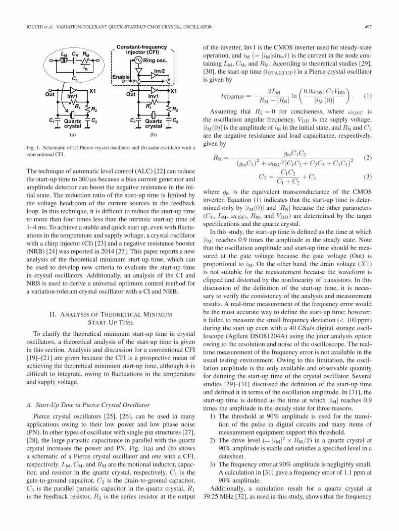
Fig. 2. Strategy to reduce the start-up time of a crystal oscillator by noise injec-tion and the use of an NRB. Temporarily increasing |iM(0+)| and |RN| reducesthe start-up time.
error is within 10 ppm at 90% amplitude. The frequency errorat 90% amplitude should be acceptable for a wireless specifica-tion [3]. In this paper, the threshold is defined as 90% amplitudefor the above reasons.
Fig. 2 shows the strategy used to reduce the start-up time,assuming that the period of noise injection (tNOISE) is neg-ligibly small. The values of |iM(0+)| and |RN| correspond tothe y-intercept (≈ y-value at t = tNOISE) and gradient of thelines in Fig. 2, respectively. To reduce the start-up time inthis study, |iM(0+)| is first increased by noise injection, whichshifts the line vertically upward. After that, |RN| is increased byemploying the NRB, which increases the gradient of the line.
B. Analysis of Theoretical Minimum Start-Up Time
Under the ideal condition without any variations, anultrahigh-accurate CFI can achieve the theoretical minimumstart-up time because the y-intercept in Fig. 2 is directly shiftedto the steady-state amplitude by the CFI. On the other hand, therate of the amplitude increase of iM by time does not increasesignificantly when the NRB excessively boosts the negativeresistance owing to the capacitance of C3 in the quartz crystal;therefore, the NRB cannot achieve the theoretical minimum.The differential rectangular signals from the ring oscillatorcharge up the resonator in the quartz crystal, and RM limits theminimum start-up time. The effect of R2 is ignored for sim-plicity because the cutoff frequency (> 1GHz) of the low-passfilter of R2 and C2 is sufficiently higher than the oscillationfrequency. The transient of iM is calculated by solving thedifferential equation
4VDD
πsinωt = LM
diM
dt+RMiM +
1
CM
∫iMdt. (4)
Assuming that the harmonics of the rectangular signalsare negligible. The differential rectangular signal is given as4VDD/π from the Fourier series at the fundamental frequency.
At ω = ω0 ≈ ωOSC, where ω0 is the series resonant fre-quency of the quartz crystal. The transient of |iM| is given by
|iM| = 4VDD
πRM
(1− e
− RM2LM
t). (5)
Equation (5) is calculated with the assumption of iM(0) = 0for simplicity. In many cases, iM(0) is negligibly small becauseiM(0) is determined by the thermal noise in the circuit. In aPierce crystal oscillator with a CMOS inverter, the amplitude of
the gate-to-ground voltage (|VG|) in the steady state is approxi-mately VDD/2. According to [33] and the definition of the startup, |iM| at the start up (|iM|STARTUP) is given by
|iM|STARTUP = 0.45ωOSCVDD (C1 + 2C3) . (6)
Assuming C1 = C2 for conciseness. By equating (5) and(6) as
4VDD
πRM
(1− e
− RM2LM
t)= 0.45ωOSCVDD (C1 + 2C3) . (7)
The theoretical minimum start-up time (tSTARTUP_MIN) for a39.25 MHz quartz crystal [32] is obtained as follows:
tSTARTUP_MIN ≈ −2LM
RMln [1− 0.35ωOSCRM (C1 + 2C3)]
= 11.1 µs. (8)
The theoretical minimum start-up time of 11.1µs is 14.2times shorter than the shortest start-up time in a state-of-the-artoscillator [23]. This implies that the upcoming techniques couldachieve a much shorter start-up time (e.g., less than 100 µs) incrystal oscillators with frequency of 10 MHz order. A CFI isnot practical because the worst-case start-up time specifies theeffective start-up time for the whole system. Both a short start-up time and small variations of the start-up time are importantfactors from the viewpoint of system design.
III. CHIRP INJECTION AND NRB
A. Overview of Crystal Oscillator With CI and NRB
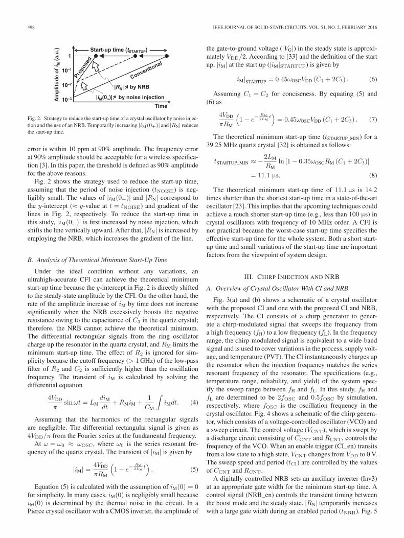
Fig. 3(a) and (b) shows a schematic of a crystal oscillatorwith the proposed CI and one with the proposed CI and NRB,respectively. The CI consists of a chirp generator to gener-ate a chirp-modulated signal that sweeps the frequency froma high frequency (fH) to a low frequency (fL). In the frequencyrange, the chirp-modulated signal is equivalent to a wide-bandsignal and is used to cover variations in the process, supply volt-age, and temperature (PVT). The CI instantaneously charges upthe resonator when the injection frequency matches the seriesresonant frequency of the resonator. The specifications (e.g.,temperature range, reliability, and yield) of the system spec-ify the sweep range between fH and fL. In this study, fH andfL are determined to be 2fOSC and 0.5fOSC by simulation,respectively, where fOSC is the oscillation frequency in thecrystal oscillator. Fig. 4 shows a schematic of the chirp genera-tor, which consists of a voltage-controlled oscillator (VCO) anda sweep circuit. The control voltage (VCNT), which is swept bya discharge circuit consisting of CCNT and RCNT, controls thefrequency of the VCO. When an enable trigger (CI_en) transitsfrom a low state to a high state, VCNT changes from VDD to 0 V.The sweep speed and period (tCI) are controlled by the valuesof CCNT and RCNT.
A digitally controlled NRB sets an auxiliary inverter (Inv3)at an appropriate gate width for the minimum start-up time. Acontrol signal (NRB_en) controls the transient timing betweenthe boost mode and the steady state. |RN| temporarily increaseswith a large gate width during an enabled period (tNRB). Fig. 5
IGUCHI et al.: VARIATION-TOLERANT QUICK-START-UP CMOS CRYSTAL OSCILLATOR 499
Fig. 3. Schematic of a crystal oscillator (a) with the proposed CI and (b) withthe proposed CI and NRB.
Fig. 4. Detailed schematic of the chirp generator consisting of a VCO and asweep circuit.
Fig. 5. Timing chart for the crystal oscillator with the proposed CI and NRB.The NRB boosts |RN| during the period denoted by tNRB because the transis-tors in Inv3 are in the linear region during the period denoted by tCI. In thisstudy, the start-up time is determined as that when the oscillation amplitudereaches 0.9 times the peak-to-peak amplitude (A) in the steady state.
shows a timing chart for the crystal oscillator with the CIand NRB. First, a wake-up signal pulls up both CI_en andNRB_en. While CI_en is high, the signal at chirp excites Outand X1. After that, the NRB with Inv3 increases |RN| duringthe period denoted by tNRB in Fig. 5. Finally, the NRB disablesthe |RN| boost when the oscillation amplitude in Out reaches
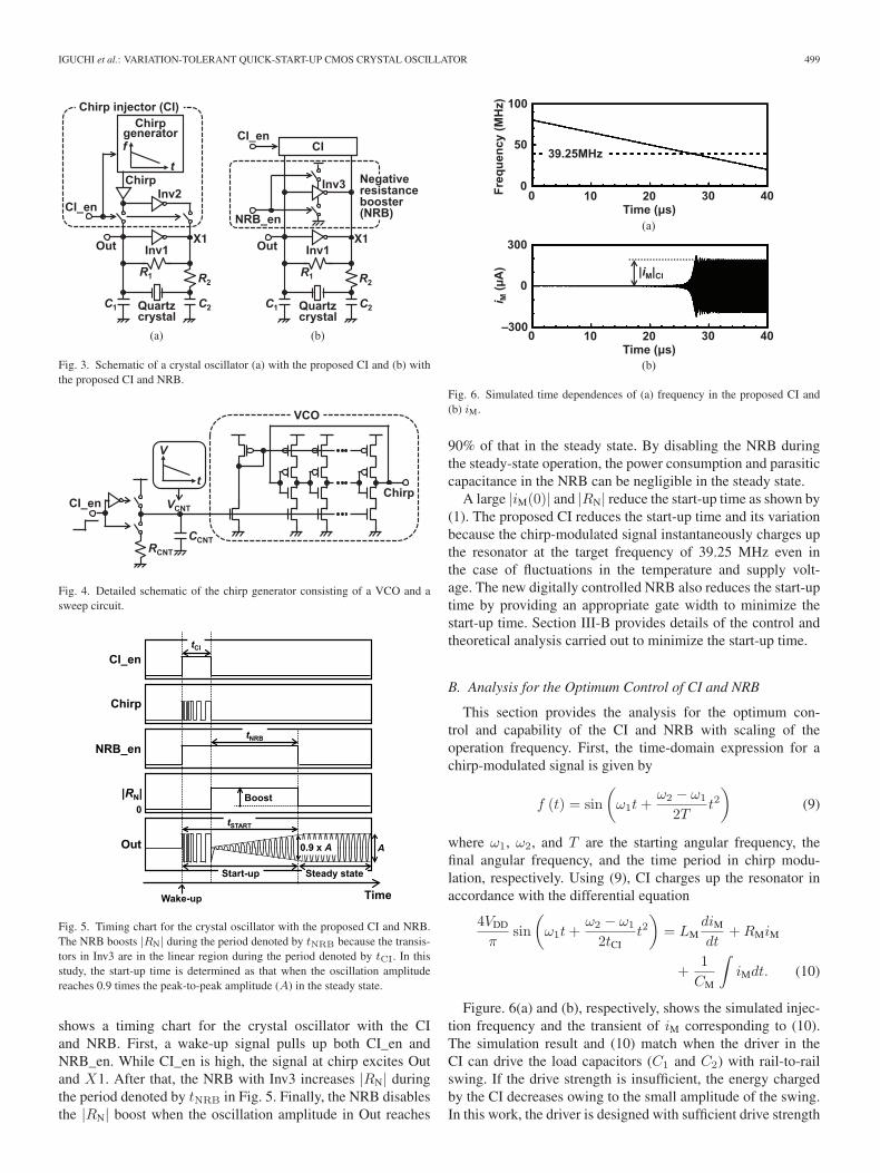
Fig. 6. Simulated time dependences of (a) frequency in the proposed CI and(b) iM.
90% of that in the steady state. By disabling the NRB duringthe steady-state operation, the power consumption and parasiticcapacitance in the NRB can be negligible in the steady state.
A large |iM(0)| and |RN| reduce the start-up time as shown by(1). The proposed CI reduces the start-up time and its variationbecause the chirp-modulated signal instantaneously charges upthe resonator at the target frequency of 39.25 MHz even inthe case of fluctuations in the temperature and supply volt-age. The new digitally controlled NRB also reduces the start-uptime by providing an appropriate gate width to minimize thestart-up time. Section III-B provides details of the control andtheoretical analysis carried out to minimize the start-up time.
B. Analysis for the Optimum Control of CI and NRB
This section provides the analysis for the optimum con-trol and capability of the CI and NRB with scaling of theoperation frequency. First, the time-domain expression for achirp-modulated signal is given by
f (t) = sin
(ω1t+
ω2 − ω1
2Tt2)
(9)
where ω1, ω2, and T are the starting angular frequency, thefinal angular frequency, and the time period in chirp modu-lation, respectively. Using (9), CI charges up the resonator inaccordance with the differential equation
4VDD
πsin
(ω1t+
ω2 − ω1
2tCIt2)
= LMdiM
dt+RMiM
+1
CM
∫iMdt. (10)
Figure. 6(a) and (b), respectively, shows the simulated injec-tion frequency and the transient of iM corresponding to (10).The simulation result and (10) match when the driver in theCI can drive the load capacitors (C1 and C2) with rail-to-railswing. If the drive strength is insufficient, the energy chargedby the CI decreases owing to the small amplitude of the swing.In this work, the driver is designed with sufficient drive strength
500 IEEE JOURNAL OF SOLID-STATE CIRCUITS, VOL. 51, NO. 2, FEBRUARY 2016
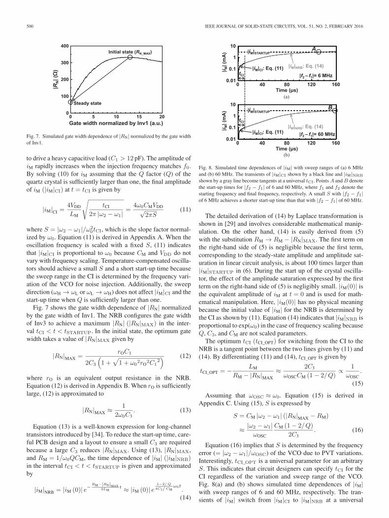
Fig. 7. Simulated gate width dependence of |RN| normalized by the gate widthof Inv1.
to drive a heavy capacitive load (C1 > 12 pF). The amplitude ofiM rapidly increases when the injection frequency matches f0.By solving (10) for iM assuming that the Q factor (Q) of thequartz crystal is sufficiently larger than one, the final amplitudeof iM (|iM|CI) at t = tCI is given by
|iM|CI =4VDD
LM
√tCI
2π |ω2 − ω1| =4ω0CMVDD√
2πS(11)
where S = |ω2 − ω1|/ω20tCI, which is the slope factor normal-
ized by ω0. Equation (11) is derived in Appendix A. When theoscillation frequency is scaled with a fixed S, (11) indicatesthat |iM|CI is proportional to ω0 because CM and VDD do notvary with frequency scaling. Temperature-compensated oscilla-tors should achieve a small S and a short start-up time becausethe sweep range in the CI is determined by the frequency vari-ation of the VCO for noise injection. Additionally, the sweepdirection (ωH → ωL or ωL → ωH) does not affect |iM|CI and thestart-up time when Q is sufficiently larger than one.
Fig. 7 shows the gate width dependence of |RN| normalizedby the gate width of Inv1. The NRB configures the gate widthof Inv3 to achieve a maximum |RN| (|RN|MAX) in the inter-val tCI < t < tSTARTUP. In the initial state, the optimum gatewidth takes a value of |RN|MAX given by
|RN|MAX =rOC1
2C3
(1 +
√1 + ω0
2rO2C1
2) (12)
where rO is an equivalent output resistance in the NRB.Equation (12) is derived in Appendix B. When rO is sufficientlylarge, (12) is approximated to
|RN|MAX ≈ 1
2ω0C3. (13)
Equation (13) is a well-known expression for long-channeltransistors introduced by [34]. To reduce the start-up time, care-ful PCB design and a layout to ensure a small C3 are requiredbecause a large C3 reduces |RN|MAX. Using (13), |RN|MAX,and RM = 1/ω0QCM, the time dependence of |iM| (|iM|NRB)in the interval tCI < t < tSTARTUP is given and approximatedby
|iM|NRB = |iM (0)| e−RM−|RN|MAX
2LMt ≈ |iM (0)| e
1−2/Q
4C3/CMω0t
.(14)
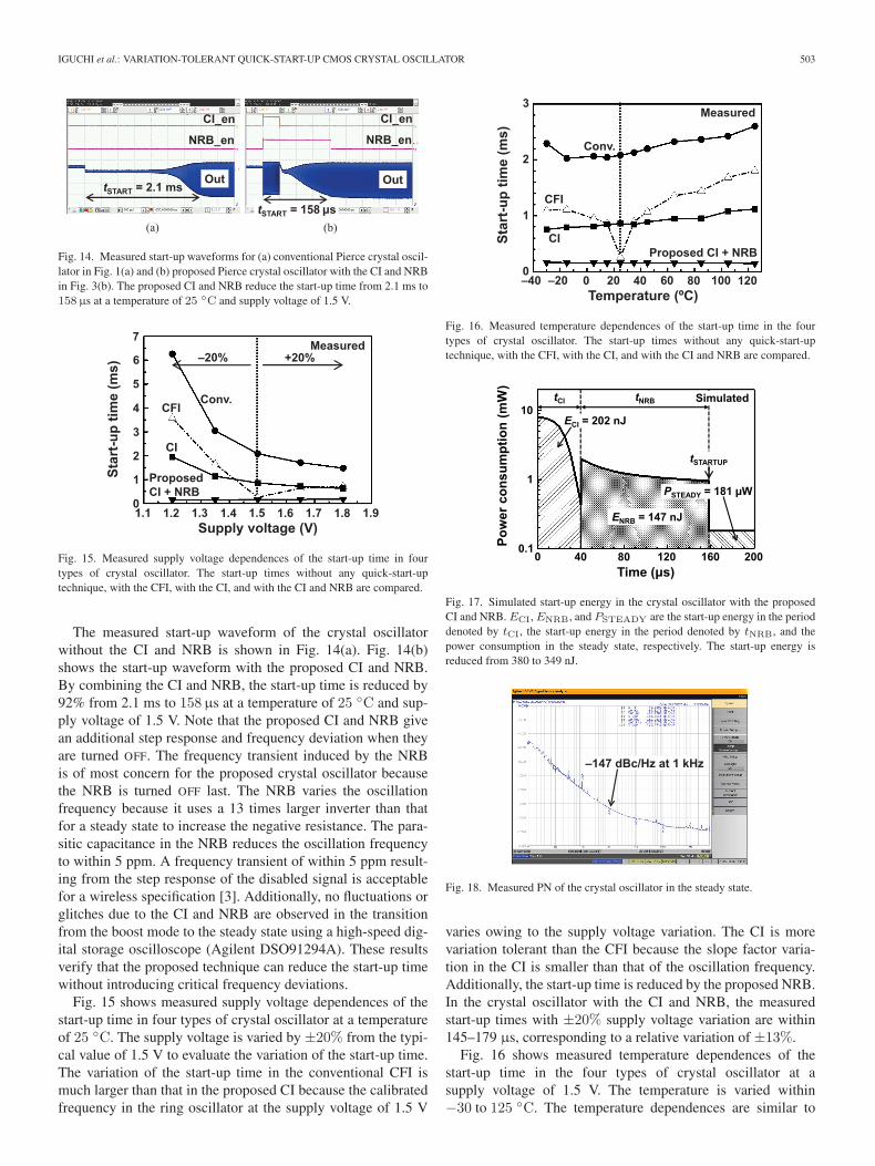
Fig. 8. Simulated time dependences of |iM| with sweep ranges of (a) 6 MHzand (b) 60 MHz. The transients of |iM|CI shown by a black line and |iM|NRB
shown by a gray line become tangents at a universal tCI. Points A and B denotethe start-up times for |f2 − f1| of 6 and 60 MHz, where f1 and f2 denote thestarting frequency and final frequency, respectively. A small S with |f2 − f1|of 6 MHz achieves a shorter start-up time than that with |f2 − f1| of 60 MHz.
The detailed derivation of (14) by Laplace transformation isshown in [29] and involves considerable mathematical manip-ulation. On the other hand, (14) is easily derived from (5)with the substitution RM → RM − |RN|MAX. The first term onthe right-hand side of (5) is negligible because the first term,corresponding to the steady-state amplitude and amplitude sat-uration in linear circuit analysis, is about 100 times larger than|iM|STARTUP in (6). During the start up of the crystal oscilla-tor, the effect of the amplitude saturation expressed by the firstterm on the right-hand side of (5) is negligibly small. |iM(0)| isthe equivalent amplitude of iM at t = 0 and is used for math-ematical manipulation. Here, |iM(0)| has no physical meaningbecause the initial value of |iM| for the NRB is determined bythe CI as shown by (11). Equation (14) indicates that |iM|NRB isproportional to exp(ω0) in the case of frequency scaling becauseQ, C3, and CM are not scaled parameters.
The optimum tCI (tCI_OPT) for switching from the CI to theNRB is a tangent point between the two lines given by (11) and(14). By differentiating (11) and (14), tCI_OPT is given by
tCI_OPT = − LM
RM − |RN|MAX
≈ 2C3
ωOSCCM (1− 2/Q)∝ 1
ωOSC.
(15)
Assuming that ωOSC ≈ ω0. Equation (15) is derived inAppendix C. Using (15), S is expressed by
S = CM |ω2 − ω1| (|RN|MAX −RM)
≈ |ω2 − ω1|ωOSC
CM (1− 2/Q)
2C3. (16)
Equation (16) implies that S is determined by the frequencyerror (= |ω2 − ω1|/ωOSC) of the VCO due to PVT variations.Interestingly, tCI_OPT is a universal parameter for an arbitraryS. This indicates that circuit designers can specify tCI for theCI regardless of the variation and sweep range of the VCO.Fig. 8(a) and (b) shows simulated time dependences of |iM|with sweep ranges of 6 and 60 MHz, respectively. The tran-sients of |iM| switch from |iM|CI to |iM|NRB at a universal

IGUCHI et al.: VARIATION-TOLERANT QUICK-START-UP CMOS CRYSTAL OSCILLATOR 501
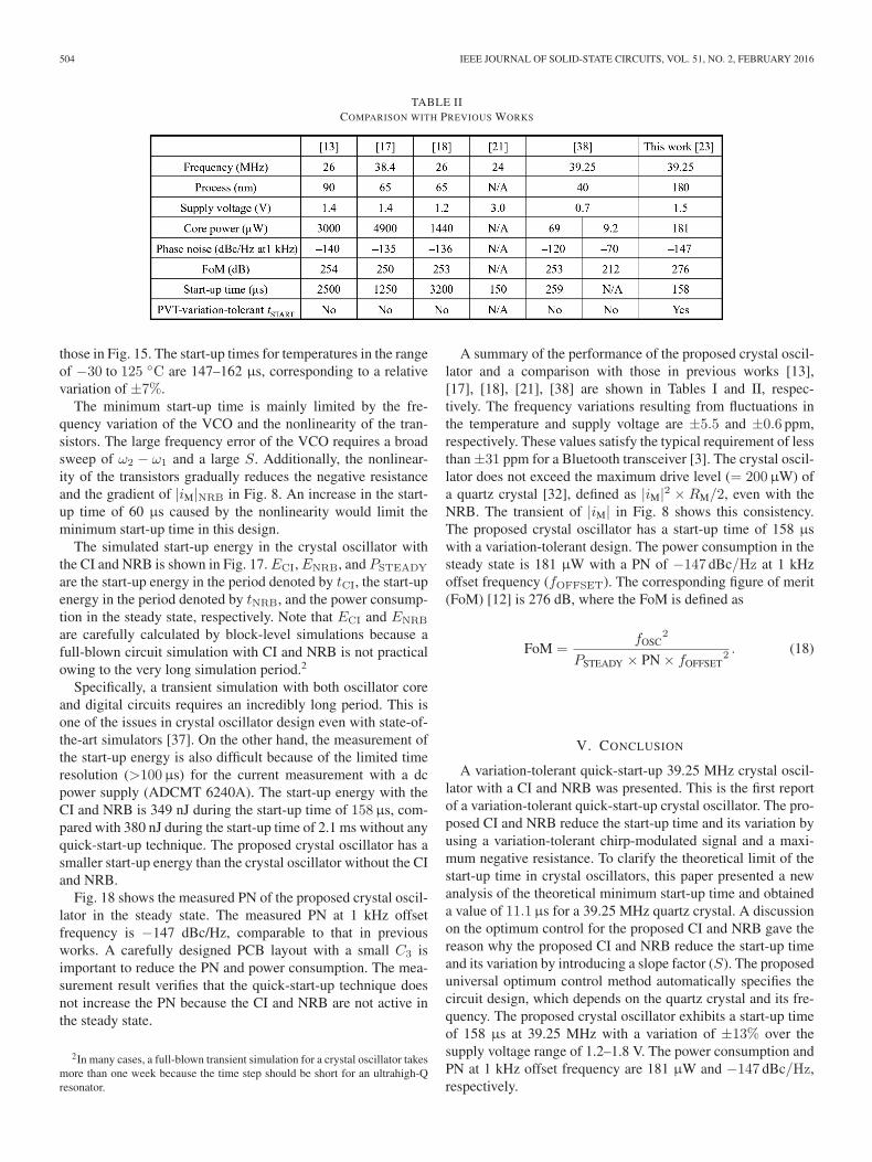
Fig. 9. Die micrograph and layout fabricated in 180 nm CMOS process.
tCI_OPT of 12.5 µs, corresponding to the tangent point, evenwith different sweep ranges. From (1), (11), (13), and (15),the start-up time (tSTART_OPT) when using the CI and NRB isgiven by
tSTARTUP_OPT = tCI_OPT
[ln
(CT
2
CM2S
)− 0.15
]∝ 1
ωOSC. (17)
Equation (17) is derived in Appendix D and verifies thattSTART_OPT does not depend on gm in Inv1 and Inv3. The rel-ative sweep range of the VCO (proportional to S) is the onlyvariable parameter for the circuit designer at a target frequency.When an accurate oscillator (e.g., relaxation oscillator) for theCI is available, a small S can be used to minimize the start-uptime because a small S increases |iM|CI. A comparison of thestart-up time with different S is shown in Fig. 8. S in Fig. 8(a) is10 times smaller than that in Fig. 8(b). The smaller S achieves ashorter start-up time because |iM|CI is closer to the steady state(≈ |iM|STARTUP) than that with the larger S. Reducing S is theonly way to reduce the start-up time from the viewpoint of cir-cuit design; otherwise, a quartz crystal with small C3 and CT
is required. Additionally, S (proportional to |ω2 − ω1|/ωOSC)does not change significantly with PVT variations because thevariation of the delay in the transistors changes ω1, ω2, andωOSC by the same ratio. The variations of RCNT and CCNT
should also be considered. Assuming ±40% variations of theRC product (approximately inversely proportional to S), thevariation of the start-up time calculated with (17) is less than±7% because the variation of S is scaled down by ln(S). That iswhy the start-up time in the proposed crystal oscillator with theCI and NRB does not change significantly with PVT variations.
Finally, noted that the approximated expressions in (13)–(17)are effective for long-channel transistors. If short-channel tran-sistors are used, the exact expressions should be adopted forcircuit optimization. Additionally, |RN| in the exact expressionsshould be estimated by simulation owing to the inaccuracy inthe modeling of rO [35].
IV. MEASUREMENT RESULTS AND DISCUSSION
To demonstrate and verify the quick-start-up operation, theproposed crystal oscillator with the CI and NRB is imple-mented as shown in Fig. 3(b); additionally, the previous CFIshown in Fig. 1(b) is also implemented in the same die to eval-uate the effects of the proposed CI and NRB. Fig. 9 showsthe die micrograph and the layout, which was fabricated in a180 nm CMOS process. Electrostatic discharge (ESD) is imple-mented with a body diode between the drain and well of thetransistors. The transistor-based structure can be simulated by
TABLE IDESIGN PARAMETERS AND PERFORMANCE SUMMARY
SPICE simulations without additional device simulations intechnology computer-aided design (TCAD). The target oscil-lation frequency of the quartz crystal is 39.25 MHz with a loadcapacitance (CT) of 8 pF [32]. The passive components (e.g.,R1, R2, C1, C2, and the quartz crystal) are implemented on anFR4 PCB. To compensate the parasitic capacitors on the PCB,the values of C1 and C2 are carefully chosen. The test chip isdirectly mounted on the PCB with an electrically conductiveepoxy. The bare chip and PCB are connected by bonding wires.
Table I shows the design parameters and a summary of theperformance of the proposed crystal oscillator. The start-uptime and power consumption without the CI and NRB are2.1 ms and 181µW, respectively. These values are compara-ble to those in other works [13]–[18] without quick-start-uptechniques. In the proposed crystal oscillator, 8 bit digitallycontrolled gate widths in Inv1 and Inv3 are used to config-ure the negative resistances in the steady-state and boost modeto obtain an oscillation allowance of more than five [36] andRN_MAX, respectively. The series resistance (R2) reduces theinjection power into the quartz crystal and prevents overtoneoscillation due to the parasitic inductors on the PCB.
The measured injection time dependence of the start-up timewith the previous CFI is shown in Fig. 10. To verify the con-sistency of the analysis in Section II, an arbitrary function gen-erator (Tektronix AFG 3251) accurately regulates the injectionfrequency within a variation of ±1 ppm. A tristate buffer in theCFI is used to vary the injection time within 0−15µs. The min-imum measured start-up time is 12.8µs. This result verifies thatthe discussion on the theoretical minimum start-up time is valid.
Fig. 11 shows the measured injection frequency dependenceof the start-up time with the previous CFI. The CFI injectsa constant-frequency signal for an injection time of 40µs.

502 IEEE JOURNAL OF SOLID-STATE CIRCUITS, VOL. 51, NO. 2, FEBRUARY 2016
Fig. 10. Measured injection time dependence of the start-up time with the pre-vious CFI. In this measurement, an arbitrary function generator (Tektronix AFG3251) generates an accurate injection signal to achieve good matching betweenthe injection frequency and the resonance frequency of the quartz crystal. Themeasurement result verifies that the theoretical analysis in Section II is valid.
Fig. 11. Measured frequency dependence of the start-up time with the previousCFI. To input an accurate injection frequency for the quartz crystal, an arbi-trary function generator (Tektronix AFG 3251) injects the injection signal foran injection time of 40µs. The variation of the start-up time is caused by thefrequency error of the ring oscillator.
The measured start-up time with the CFI varies within 40–1067 µs depending on the injection frequency, which variesin the range 38.0–40.5 MHz. The measured frequency varia-tion of the embedded ring oscillator in the CFI is ±9% overthe temperature range of −30 to 125 ◦C at the supply voltageof 1.5 V. The start-up time in the case of 0.1% variation varieswithin 40−500µs. A crystal oscillator [21] with 0.25% varia-tion using a temperature-compensated RC oscillator achieves ashorter start-up time; however, this implies that a variation of0.25% causes the start-up time to vary.
Measured time dependences of the chirp frequency in thechirp generator are shown in Fig. 12. To compensate the effectof the parasitic capacitances on the PCB, the target tCI is setto 40 µs using (15). The design target of the initial frequencyat a typical corner is 80 MHz. The chirp frequency crosses theoscillation frequency of the crystal oscillator over the best andworst corners in the test chip. The measured oscillation fre-quency in the VCO is 16% lower than the simulated frequencyowing to model mismatches and process variations. This testchip matches the case of a slow transistor model in a processdesign kit (PDK). This verifies that the chirp frequency crosses39.25 MHz even in the worst case (= 1.35V, 125 ◦C, slowdevice).
Fig. 12. Measured time dependences of the frequency in the proposed CI atthree corners. All lines cross the target frequency of 39.25 MHz once beforetCI = 40µs.
Fig. 13. Measured gate width dependences of the start-up time and the powerconsumption of the proposed NRB in the steady state with infinite tNRB. Thegate width for the NRB is normalized by that of Inv1.
Fig. 13 shows the measured gate width dependences of thestart-up time and the power consumption of the NRB in thesteady state with a disabled CI and infinite tNRB. The gate widthfor the NRB is normalized by that of Inv1. With increasing thegate width, |RN| increases and the start-up time decreases atthe cost of increasing the power consumption. The NRB inthe proposed crystal oscillator uses a normalized gate widthof 13, corresponding to the maximum |RN|, which minimizesthe start-up time because the aim of this study is to clarifythe theoretical limitation of the start-up time with the CI andNRB. Additionally, the slow start-up time increases the systemlatency from the standby mode to the active mode in an RF SoC.If the start-up energy is the most important factor for the sys-tem, the optimum gate width will be smaller than the gate widthused in this paper because the start-up time at a gate width of5–10 is not significantly larger than the minimum start-up time.The optimum gate width should be determined from the totalstart-up energy and the latency in the whole system. In this case,the start-up time is reduced by 87%, while the power consump-tion increases by a factor of 4.9. In the measurements, the NRBis disabled at the time that the gate voltage at Inv1 reaches 0.9times the amplitude in the steady state. A comparator or Schmitttrigger could be used to detect and disable the NRB dependingon the oscillation amplitude. The optimum gate width is deter-mined as the gate width corresponding to the maximum |RN|,which minimizes the start-up time of the crystal oscillator.
IGUCHI et al.: VARIATION-TOLERANT QUICK-START-UP CMOS CRYSTAL OSCILLATOR 503
Fig. 14. Measured start-up waveforms for (a) conventional Pierce crystal oscil-lator in Fig. 1(a) and (b) proposed Pierce crystal oscillator with the CI and NRBin Fig. 3(b). The proposed CI and NRB reduce the start-up time from 2.1 ms to158µs at a temperature of 25 ◦C and supply voltage of 1.5 V.
Fig. 15. Measured supply voltage dependences of the start-up time in fourtypes of crystal oscillator. The start-up times without any quick-start-uptechnique, with the CFI, with the CI, and with the CI and NRB are compared.
The measured start-up waveform of the crystal oscillatorwithout the CI and NRB is shown in Fig. 14(a). Fig. 14(b)shows the start-up waveform with the proposed CI and NRB.By combining the CI and NRB, the start-up time is reduced by92% from 2.1 ms to 158µs at a temperature of 25 ◦C and sup-ply voltage of 1.5 V. Note that the proposed CI and NRB givean additional step response and frequency deviation when theyare turned OFF. The frequency transient induced by the NRBis of most concern for the proposed crystal oscillator becausethe NRB is turned OFF last. The NRB varies the oscillationfrequency because it uses a 13 times larger inverter than thatfor a steady state to increase the negative resistance. The para-sitic capacitance in the NRB reduces the oscillation frequencyto within 5 ppm. A frequency transient of within 5 ppm result-ing from the step response of the disabled signal is acceptablefor a wireless specification [3]. Additionally, no fluctuations orglitches due to the CI and NRB are observed in the transitionfrom the boost mode to the steady state using a high-speed dig-ital storage oscilloscope (Agilent DSO91294A). These resultsverify that the proposed technique can reduce the start-up timewithout introducing critical frequency deviations.
Fig. 15 shows measured supply voltage dependences of thestart-up time in four types of crystal oscillator at a temperatureof 25 ◦C. The supply voltage is varied by ±20% from the typi-cal value of 1.5 V to evaluate the variation of the start-up time.The variation of the start-up time in the conventional CFI ismuch larger than that in the proposed CI because the calibratedfrequency in the ring oscillator at the supply voltage of 1.5 V
Fig. 16. Measured temperature dependences of the start-up time in the fourtypes of crystal oscillator. The start-up times without any quick-start-uptechnique, with the CFI, with the CI, and with the CI and NRB are compared.
Fig. 17. Simulated start-up energy in the crystal oscillator with the proposedCI and NRB. ECI, ENRB, and PSTEADY are the start-up energy in the perioddenoted by tCI, the start-up energy in the period denoted by tNRB, and thepower consumption in the steady state, respectively. The start-up energy isreduced from 380 to 349 nJ.
Fig. 18. Measured PN of the crystal oscillator in the steady state.
varies owing to the supply voltage variation. The CI is morevariation tolerant than the CFI because the slope factor varia-tion in the CI is smaller than that of the oscillation frequency.Additionally, the start-up time is reduced by the proposed NRB.In the crystal oscillator with the CI and NRB, the measuredstart-up times with ±20% supply voltage variation are within145–179 µs, corresponding to a relative variation of ±13%.
Fig. 16 shows measured temperature dependences of thestart-up time in the four types of crystal oscillator at asupply voltage of 1.5 V. The temperature is varied within−30 to 125 ◦C. The temperature dependences are similar to
504 IEEE JOURNAL OF SOLID-STATE CIRCUITS, VOL. 51, NO. 2, FEBRUARY 2016
TABLE IICOMPARISON WITH PREVIOUS WORKS
those in Fig. 15. The start-up times for temperatures in the rangeof −30 to 125 ◦C are 147–162 µs, corresponding to a relativevariation of ±7%.
The minimum start-up time is mainly limited by the fre-quency variation of the VCO and the nonlinearity of the tran-sistors. The large frequency error of the VCO requires a broadsweep of ω2 − ω1 and a large S. Additionally, the nonlinear-ity of the transistors gradually reduces the negative resistanceand the gradient of |iM|NRB in Fig. 8. An increase in the start-up time of 60 µs caused by the nonlinearity would limit theminimum start-up time in this design.
The simulated start-up energy in the crystal oscillator withthe CI and NRB is shown in Fig. 17. ECI, ENRB, and PSTEADY
are the start-up energy in the period denoted by tCI, the start-upenergy in the period denoted by tNRB, and the power consump-tion in the steady state, respectively. Note that ECI and ENRB
are carefully calculated by block-level simulations because afull-blown circuit simulation with CI and NRB is not practicalowing to the very long simulation period.2
Specifically, a transient simulation with both oscillator coreand digital circuits requires an incredibly long period. This isone of the issues in crystal oscillator design even with state-of-the-art simulators [37]. On the other hand, the measurement ofthe start-up energy is also difficult because of the limited timeresolution (>100µs) for the current measurement with a dcpower supply (ADCMT 6240A). The start-up energy with theCI and NRB is 349 nJ during the start-up time of 158µs, com-pared with 380 nJ during the start-up time of 2.1 ms without anyquick-start-up technique. The proposed crystal oscillator has asmaller start-up energy than the crystal oscillator without the CIand NRB.
Fig. 18 shows the measured PN of the proposed crystal oscil-lator in the steady state. The measured PN at 1 kHz offsetfrequency is −147 dBc/Hz, comparable to that in previousworks. A carefully designed PCB layout with a small C3 isimportant to reduce the PN and power consumption. The mea-surement result verifies that the quick-start-up technique doesnot increase the PN because the CI and NRB are not active inthe steady state.
2In many cases, a full-blown transient simulation for a crystal oscillator takesmore than one week because the time step should be short for an ultrahigh-Qresonator.
A summary of the performance of the proposed crystal oscil-lator and a comparison with those in previous works [13],[17], [18], [21], [38] are shown in Tables I and II, respec-tively. The frequency variations resulting from fluctuations inthe temperature and supply voltage are ±5.5 and ±0.6 ppm,respectively. These values satisfy the typical requirement of lessthan ±31 ppm for a Bluetooth transceiver [3]. The crystal oscil-lator does not exceed the maximum drive level (= 200µW) ofa quartz crystal [32], defined as |iM|2 ×RM/2, even with theNRB. The transient of |iM| in Fig. 8 shows this consistency.The proposed crystal oscillator has a start-up time of 158 µswith a variation-tolerant design. The power consumption in thesteady state is 181 µW with a PN of −147 dBc/Hz at 1 kHzoffset frequency (fOFFSET). The corresponding figure of merit(FoM) [12] is 276 dB, where the FoM is defined as
FoM =fOSC
2
PSTEADY × PN × fOFFSET2 . (18)
V. CONCLUSION
A variation-tolerant quick-start-up 39.25 MHz crystal oscil-lator with a CI and NRB was presented. This is the first reportof a variation-tolerant quick-start-up crystal oscillator. The pro-posed CI and NRB reduce the start-up time and its variation byusing a variation-tolerant chirp-modulated signal and a maxi-mum negative resistance. To clarify the theoretical limit of thestart-up time in crystal oscillators, this paper presented a newanalysis of the theoretical minimum start-up time and obtaineda value of 11.1µs for a 39.25 MHz quartz crystal. A discussionon the optimum control for the proposed CI and NRB gave thereason why the proposed CI and NRB reduce the start-up timeand its variation by introducing a slope factor (S). The proposeduniversal optimum control method automatically specifies thecircuit design, which depends on the quartz crystal and its fre-quency. The proposed crystal oscillator exhibits a start-up timeof 158 µs at 39.25 MHz with a variation of ±13% over thesupply voltage range of 1.2–1.8 V. The power consumption andPN at 1 kHz offset frequency are 181 µW and −147 dBc/Hz,respectively.

IGUCHI et al.: VARIATION-TOLERANT QUICK-START-UP CMOS CRYSTAL OSCILLATOR 505
APPENDIX ADERIVATION OF (11)
In this appendix, (11) is derived. Equation (11) is derived bysolving the differential equation of (10). First, the left-hand sideof (10) is transformed to
V =4VDD
πsin
(ω1t+
ω2 − ω1
2tCIt2)
=4VDD
πsin
(ω′
1t′ +
ω′2 − ω′
1
2t′CIt′2
) (A1)
with the normalized expressions
t′ =t√
LMCM(A2)
ω′ = ω√LMCM (A3)
t′CI =tCI√LMCM
. (A4)
Equation (A1) is differentiated with respect to t′ as
dV
dt′=
4VDD
π
(ω′
1 +ω′
2 − ω′1
t′CIt′)cos
(ω′
1t′ +
ω′2 − ω′
1
2t′CIt′2).
(A5)
The substitution of ω′1 → 0 and ω′
2 → ω′2 − ω′
1 simplifies(A5) to
dV
dt′=
4VDD
π
(ω′
2 − ω′1
t′CIt′)cos
(ω′
2 − ω′1
2t′CIt′2
)(A6)
where a normalized slope factor (S) is defined as
S =ω2 − ω1
tCI× LMCM =
ω′2 − ω′
1
t′CI. (A7)
By introducing the slope factor into (A6), the derivative ofthe left-hand side of (10) becomes
dV
dt′=
4VDDSt′
πcos
(S
2t′2
). (A8)
The derivative of the right-hand side of (10)
dV
dt= LM
d2iM
dt2+RM
diM
dt+
iM
CM(A9)
is transformed by (A2) to
d2iM
dt′2+RM
√CM
LM
diM
dt′+ iM =
√CM
LM
dV
dt′. (A10)
By substituting (A8) into (A10), (10) becomes
d2iM
dt′2+RM
√CM
LM
diM
dt′+ iM =
√CM
LM
4VDDSt′
πcos
(S
2t′2).
(A11)
Equation (A11) is simplified to
d2i′Mdt′2
+1
Q
di′Mdt′
+ i′M = St′ cos(S
2t′2
)(A12)
with the normalized expression
i′M =π
4VDD
√LM
CMiM. (A13)
When Q is sufficiently larger than one, (A12) is approxi-mated to
d2i′Mdt′2
+ i′M ≈ St′ cos(S
2t′2
). (A14)
The normalized final amplitude (|i′M|CI) is calculated bysolving (A14) with respect to t′. However, the complete expres-sion for the solution of (A14) is too complex to describehere because it includes many Fresnel integrals. |i′M|CI cor-responding to the amplitude of the solution at infinite t′ isgiven by
|i′M|CI =
√π
2S. (A15)
Finally, (11) is derived as
|iM|CI =4ω0CMVDD√
2πS(A16)
by substituting (A13) into (A15).
APPENDIX BDERIVATION OF (12)
In this appendix, (12) is derived. When the effect of anequivalent output resistance (rO) in the inverter is assumed, thenegative resistance is given as
|RN| = rOC12
C12(1+ω0
2rO2C1
2)gmrO−1 + 2C1C3 + C3
2 (gmrO − 1)(B1)
with C1 = C2. Here, the function f(gm) = |RN| is defined. Thederivative of f(gm) with respect to gm is equated to zero
f ′ (gm) = 0 (B2)
to calculate the maximum value of |RN|. Then, the solution of(B2) corresponding to the optimum value of gm (gm_OPT) forthe NRB is given by
gm_OPT =C3 + C1
√1 + ω2rO
2C12
rOC3. (B3)
By substituting (B3) into (B1), the maximum value of thenegative resistance (|RN|MAX) is obtained as
|RN|MAX =rOC1
2C3
(1 +
√1 + ω0
2rO2C1
2) . (B4)

506 IEEE JOURNAL OF SOLID-STATE CIRCUITS, VOL. 51, NO. 2, FEBRUARY 2016
Fig. 19. Time dependences of |iM| with tCI of (a) 12.5 µs and (b) 60µs calcu-lated using (11) and (14) with |f2 − f1| = 60MHz. The shortest start-up timeis achieved at tCI of 12.5µs, corresponding to the tangent point of two lines.
APPENDIX CDERIVATION OF (15)
In this appendix, (15) is derived. First, it is verified thatthe optimum tCI (tCI_OPT) is determined at a tangent pointbetween the two lines given by (11) and (14). Fig. 19(a) and(b) shows the time dependences of |iM| with tCI of 12.5 and60 µs calculated using (11) and (14) with |f2 − f1| = 60MHz.The calculated dependences verify that the start-up time is min-imized at tCI of 12.5 µs, corresponding to the tangent pointbecause |iM(0)| in (14) becomes the maximum value at tCI of12.5µs. Note that (11) in Fig. 19 does not include the effectof the nonlinearity of the transistors and that the calculatedstart-up time is shorter than that in Fig. 8. The start-up timein Fig. 19(a) corresponds to that calculated by extrapolating|iM|NRB in Fig. 8(b).
The tangent point is derived from (11) and (14) using thisfinding. To find the optimum tCI, |iM(0)| is calculated byequating (11) and (14) as follows:
4VDD
LM
√t
2π |ω2 − ω1| = |iM (0)| e−RM−|RN|MAX
2LMt (C1)
|iM (0)| = 4VDD
LM
√t
2π |ω2 − ω1|eRM−|RN|MAX
2LMt. (C2)
To derive the tangent point, the derivatives of (11) and (14)with respect to t are calculated as
d|iM|CI
dt=
2VDD
LM
1√2πt |ω2 − ω1|
(C3)
d|iM|NRB
dt= −RM − |RN|MAX
2LM|iM (0)| e−
RM−|RN|MAX2LM
t. (C4)
Equation (C4) is simplified by substituting (C2) into (C4) togive
d|iM|NRB
dt= −2VDD
LM2 (RM − |RN|MAX)
√t
2π |ω2 − ω1| . (C5)
By equating (C3) and (C5), the optimum tCI (tCI_OPT) cor-responding the tangent point between the two lines given by(11) and (14) is derived as
tCI_OPT = − LM
RM − |RN|MAX
. (C6)
APPENDIX DDERIVATION OF (17)
In this appendix, (17) is derived. Equations (11) and (14) areequated at t = tCI_OPT as
4ω0CMVDD√2πS
= |iM (0)| e−RM−|RN|MAX
2LM
(− LM
RM−|RN|MAX
). (D1)
Then, |iM(0)| is given by
|iM (0)| = 4ω0CMVDD√2πeS
. (D2)
Substituting (D2) into (1) and using (15), the start-up time isderived as
tSTARTUP = − 2LM
RM − |RN| ln(0.9ωOSCCTVDD
|iM (0)|)
= 2tCI_OPT ln
(0.9CT
√2πeS
4CM
)
= tCI_OPT
[ln
(C2
T
C2MS
)+ ln
(0.92 × 2πe
42
)]
≈ tCI_OPT
[ln
(C2
T
C2MS
)− 0.15
]. (D3)
ACKNOWLEDGMENT
The authors thank Mr. R. Shidachi of the University of Tokyofor the support in measurements.
REFERENCES
[1] A. M. Nicolson, “Generating and transmitting electric currents,” U.S.Patent 2 212 845, Aug. 27, 1940.
[2] W. G. Cady, “Method of maintaining electric currents of constant fre-quency,” U.S. Patent 1 472 583, Oct. 30, 1923.
[3] Bluetooth Special Interest Group (SIG). (2014). Specification of theBluetooth System, Core Package Version 4.2, Bluetooth Specifications,Bluetooth Special Interest Group (SIG) [Online]. Available: https://www.bluetooth.org/en-us/specification/adopted-specifications/Core_v4.2.pdf
[4] Part 11: Wireless LAN Medium Access Control (MAC) and PhysicalLayer (PHY) Specifications, IEEE Standard 802.11TM-2007, IEEE802.11 Specifications, IEEE, 2012 [Online]. Available: http://standards.ieee.org/getieee802/download/802.11-2012.pdf
IGUCHI et al.: VARIATION-TOLERANT QUICK-START-UP CMOS CRYSTAL OSCILLATOR 507
[5] K.-J. Hsiao, “A 32.4 ppm/◦C 3.2-1.6V self-chopped relaxation oscillatorwith adaptive supply generation,” in IEEE Symp. VLSI Circuits Dig. Tech.Papers, Jun. 2012, pp. 14–15.
[6] D. Griffith, P.T. Røine, J. Murdock, and R. Smith, “A 190nW 33 kHz RCoscillator with ±0.21% temperature stability and 4 ppm long-term sta-bility,” in IEEE Int. Solid-State Circuits Conf. (ISSCC) Dig. Tech. Papers,Feb. 2014, pp. 300–301.
[7] Y. Satoh, H. Kobayashi, T. Miyaba, and S. Kousai, “A 2.9 mW, +/- 85 ppmaccuracy reference clock generator based on RC oscillator with on-chiptemperature calibration,” in IEEE Symp. VLSI Circuits Dig. Tech. Papers,Jun. 2014, pp. 238–239.
[8] C. S. Lam, “A review of the recent development of MEMS and crystaloscillators and their impacts on the frequency control products industry,”in Proc. IEEE Ultrason. Symp., Nov. 2008, pp. 694–704.
[9] R. M. Cerda, Understanding Quartz Crystals and Oscillators, 1st ed.Norwood, MA, USA: Artech House, 2014.
[10] S. B. Nasir, S. Gangopadhyay, and A. Raychowdhury, “A 0.13 µm fullydigital low-dropout regulator with adaptive control and reduced dynamicstability for ultra-wide dynamic range,” in IEEE Int. Solid-State CircuitsConf. (ISSCC) Dig. Tech. Papers, Feb. 2015, pp. 98–99.
[11] Y.-H. Lee et al., “A low quiescent current asynchronous digital-LDO withPLL-modulated fast-DVS power management in 40 nm SoC for MIPSperformance improvement,” IEEE J. Solid-State Circuits, vol. 48, no. 4,pp. 1018–1030, Apr. 2013.
[12] B. Razavi, RF Microelectronics, 2nd ed. Upper Saddle River, NJ, USA:Pearson Education, Inc., 2012.
[13] J. Lin, “A low-phase-noise 0.004-ppm/step DCXO with guaranteedmonotonicity in the 90-nm CMOS process,” IEEE J. Solid-State Circuits,vol. 40, no. 12, pp. 2726–2734, Dec. 2005.
[14] S. Farahvash, C. Quek, and M. Mak, “A temperature-compensateddigitally-controlled crystal Pierce oscillator for wireless applications,”in IEEE Int. Solid-State Circuits Conf. (ISSCC) Dig. Tech. Papers, Feb.2008, pp. 352–353.
[15] M.-D. Tsai, C.-W. Yeh, Y.-H. Cho, L.-W. Ke, P.-W. Chen, and G.-K. Dehng, “A temperature-compensated low-noise digitally-controlledcrystal oscillator for multi-standard applications,” in IEEE Radio Freq.Integr. Circuits Conf. Dig. Tech. Papers, Jun. 2008, pp. 533–536.
[16] R. van Langevelde, M. van Elzakker, D. van Goor, H. Termeer, J. Moss,and A. J. Davie, “An ultra-low-power 868/915 MHz RF transceiverfor wireless sensor network applications,” in IEEE Radio Freq. Integr.Circuits Conf. Dig. Tech. Papers, Jun. 2009, pp. 113–116.
[17] D. Griffith, F. Dulger, G. Feygin, A. N. Mohieldin, and P. Vallur, “A65 nm CMOS DCXO system for generating 38.4 MHz and a real timeclock from a single crystal in 0.09mm2,” in IEEE Radio Freq. Integr.Circuits Conf. Dig. Tech. Papers, May 2010, pp. 321–324.
[18] Y. Chang, J. Leete, Z. Zhou, M. Vadipour, Y. Chang, and H. Darabi, “Adifferential digitally controlled crystal oscillator with a 14-bit tuning reso-lution and sine wave outputs for cellular applications,” IEEE J. Solid-StateCircuits, vol. 47, no. 2, pp. 421–434, Feb. 2012.
[19] S. A. Blanchard, “Quick start crystal oscillator circuit,” in Proc. IEEEUniv./Govt./Ind. Microelectron. Symp., Jun. 2003, pp. 78–81.
[20] Y.-I. Kwon, S.-G. Park, T.-J. Park, K.-S. Cho, and H.-Y. Lee, “Anultra low-power CMOS transceiver using various low-power techniquesfor LR-WPAN applications,” IEEE Trans. Circuits Syst. I, Reg. Papers,vol. 59, no. 2, pp. 324–336, Feb. 2012.
[21] Texas Instruments. (2015). CC2650 SimpleLink Multistandard WirelessMCU, CC2650 Data Sheet, Texas Instruments [Online]. Available: http://www.ti.com/lit/ds/symlink/cc2650.pdf
[22] U. Karthaus, “A differential two-pin crystal oscillator—Concept, anal-ysis, and implementation,” IEEE Trans. Circuits Syst. II, Exp. Briefs,vol. 53, no. 10, pp. 1073–1077, Oct. 2006.
[23] S. Iguchi, H. Fuketa, T. Sakurai, and M. Takamiya, “92% Start-up timereduction by variation-tolerant chirp injection (CI) and negative resistancebooster (NRB) in 39 MHz crystal oscillator,” in IEEE Symp. VLSI CircuitsDig. Tech. Papers, Jun. 2014, pp. 236–237.
[24] M. Lin, “Fast wake-up crystal oscillating circuit,” U.S. Patent 7 138 881,Nov. 21, 2006.
[25] G. W. Pierce, “Electrical system,” U.S. Patent 2 133 642, Oct. 18, 1938.[26] E. A. Vittoz, M. G. R. Degrauwe, and B. Serge, “High-performance
crystal oscillator circuits: Theory and application,” IEEE J. Solid-StateCircuits, vol. 23, no. 3, pp. 774–783, Jun. 1988.
[27] J. K. Clapp, “An inductance-capacitance oscillator of unusual frequencystability,” Proc. IRE, vol. 36, no. 3, pp. 356–358, Mar. 1948.
[28] J. T. Santos and R. G. Meyer, “A one-pin crystal oscillator for VLSIcircuits,” IEEE J. Solid-State Circuits, vol. 19, no. 2, pp. 228–236, Apr.1984.
[29] A. Rusznyak, “Start-up time of CMOS oscillators,” IEEE Trans. CircuitsSyst., vol. 34, no. 3, pp. 259–268, Jan. 1987.
[30] M. Toki and Y. Tsuzuki, “Analysis of start-up characteristics of CMOScrystal oscillators,” in Proc. IEEE Freq. Control Symp., May 1992,pp. 448–452.
[31] J. Lu, S. Onishi, and Y. Tsuzuki, “A discussion on start-up time of crystaloscillators,” (in Japanese), IEE J. Trans. Electron. Inf. Syst., vol. 111-C,no. 9, pp. 384–389, Sep. 1991.
[32] Daishinku Corp. SMD Crystal Resonators / MHz Band CrystalResonators, DSX221G Data Sheet [Online]. Available: https://www.kds.info/data/pdf/015E.pdf
[33] E. Vittoz, Low-Power Crystal and MEMS Oscillators, 1st ed. New York,NY, USA: Springer, 2010.
[34] W. M. C. Sansen, Analog Design Essentials, 1st ed. New York, NY, USA:Springer, 2006.
[35] T. Chan Carusone, D. Johns, and K. Martin, Analog Integrated CircuitDesign, 2nd ed. Hoboken, NJ, USA: Wiley, 2011.
[36] Seiko Epson Corp. Oscillator Circuit Evaluation Method (2), Technicalnotes [Online]. Available: http://www5.epsondevice.com/en/information/technical_info/pdf/tech_notes_e_oscillator_circuit_evaluation_method_2.pdf
[37] Cadence Design Systems. (2012). Simulating Crystal Oscillators is MuchEasier in MMSIM12.1—Part 2 [Online]. Available: http://community.cadence.com/cadence_blogs_8/b/rf/archive/2012/12/20/mmsim12-1-speed-up-transient-analysis-of-crystal-oscillators
[38] S. Iguchi, A. Saito, Y. Zheng, K. Watanabe, T. Sakurai, and M. Takamiya,“93% power reduction by automatic self power gating (ASPG) and mul-tistage inverter for negative resistance (MINR) in 0.7V, 9.2 µW, 39 MHzcrystal oscillator,” in IEEE Symp. VLSI Circuits Dig. Tech. Papers, Jun.2013, pp. C142–C143.
Shunta Iguchi (S’12) received the B.S. degree inelectronic engineering from the University of Electro-Communications, Tokyo, Japan, in 2011, and theM.S. degree in electrical engineering and informa-tion systems from the University of Tokyo, Tokyo,Japan, in 2013, where he is currently pursuing thePh.D. degree.
From August 2011 to September 2011, he workedwith Analog Devices, Tokyo, Japan. From August2013 to September 2013, he worked with Toshiba,Kawasaki, Japan. From August 2014 to October
2014, he worked with Taiwan Semiconductor Manufacturing Company Limited(TSMC), Hsinchu, Taiwan. His research interests include the design of low-power RF transceiver circuits, crystal oscillators, and wireless power transmis-sion circuits.
Mr. Iguchi is the recipient of the Best Paper Award at the 2013 IEEE WirelessPower Transfer Conference.
Hiroshi Fuketa (S’07–M’10) received the B.E.degree in electrical and electronic engineering fromKyoto University, Kyoto, Japan, in 2002, and theM.E. and Ph.D. degrees in information systems engi-neering from Osaka University, Osaka, Japan, in 2008and 2010, respectively.
From 2010 to 2015, he was a Research Associatewith the Institute of Industrial Science, University ofTokyo, Tokyo, Japan. Since April 2015, he has beenworking with the Nanoelectronics Research Institute,National Institute of Advanced Industrial Science and
Technology (AIST), Ibaraki, Japan. His research interests include ultra-low-power circuit design and large-area electronics with organic transistors.
Dr. Fuketa is a member of IEICE.
Takayasu Sakurai (S’77–M’78–SM’01–F’03)received the Ph.D. degree in electrical engineeringfrom the University of Tokyo, Tokyo, Japan, in 1981.
In 1981, he joined Toshiba Corporation, Tokyo,Japan, where he designed CMOS DRAM, SRAM,RISC processors, DSPs, and SoC solutions. He hasworked extensively on interconnect delay and capac-itance modeling known as Sakurai model and alphapower-law MOS model. From 1988 to 1990, he wasa Visiting Researcher at the University of California,Berkeley, CA, USA, where he conducted research in
the field of VLSI CAD. From 1996, he has been a Professor with the Universityof Tokyo, working on low-power high-speed VLSI, memory design, intercon-nects, ubiquitous electronics, organic ICs, and large-area electronics. He is a

508 IEEE JOURNAL OF SOLID-STATE CIRCUITS, VOL. 51, NO. 2, FEBRUARY 2016
Domain Research Supervisor for nano-electronics area in Japan Science andTechnology Agency, Tokyo, Japan. He has authored more than 600 technicalpublications including 100 invited presentations and several books, and filedmore than 200 patents.
Dr. Sakurai is an IEICE Fellow. He was the Executive Committee Chair forVLSI Symposia and a Steering Committee Chair for the IEEE A-SSCC. Heserved as a Conference Chair for the Symposium on VLSI Circuits and ICICDT,a Vice Chair for ASPDAC, a TPC Chair for the A-SSCC and VLSI Symposium,an Executive Committee Member for ISLPED, and a Program CommitteeMember for ISSCC, CICC, A-SSCC, DAC, ESSCIRC, ICCAD, ISLPED, andother international conferences. He was an elected AdCom Member for theIEEE Solid-State Circuits Society, and the IEEE CAS and SSCS DistinguishedLecturer. He is the recipient of the 2010 IEEE Donald O. Pederson Award inSolid-State Circuits, the 2009 and 2010 IEEE Paul Rappaport Award, the 2010IEICE Electronics Society Award, 2009 IEICE achievement Award, the 2005IEEE ICICDT Award, the 2004 IEEE Takuo Sugano Award, and the 2005 P&IPatent of the Year Award, and four product awards. He was a keynote speakerat more than 50 conferences including ISSCC, ESSCIRC, and ISLPED.
Makoto Takamiya (S’98–M’00–SM’14) receivedthe B.S., M.S., and Ph.D. degrees in electronic engi-neering from the University of Tokyo, Tokyo, Japan,in 1995, 1997, and 2000, respectively.
In 2000, he joined NEC Corporation, Tokyo, Japan,where he was engaged in the circuit design of high-speed digital LSIs. In 2005, he joined the Universityof Tokyo, where he is an Associate Professor of VLSIDesign and Education Center. From 2013 to 2014,he stayed at the University of California, Berkeley,CA, USA, as a Visiting Scholar. His research interests
include the circuit design of the low-power RF circuits, the ultra low-voltagelogic circuits, the low-voltage power management circuits, and the large-areaand flexible electronics with organic transistors.
Dr. Takamiya is a member of the Technical Program Committee of the IEEEInternational Solid-State Circuits Conference and the IEEE Symposium onVLSI Circuits. He was the recipient of the 2009 and 2010 IEEE Paul RappaportAwards and the Best Paper Award in 2013 IEEE Wireless Power TransferConference.