Embed Size (px)
Citation preview
A Bang-Bang All-Digital PLL for Frequency Synthesis
by
Joshua Zazzera
A Thesis Presented in Partial Fulfillment
of the Requirements for the Degree
Master of Science
Approved January 2012 by the
Graduate Supervisory Committee:
Bertan Bakkaloglu, Chair
Hongjiang Song
Sule Ozev
ARIZONA STATE UNIVERSITY
May 2012
i
ABSTRACT
Phase locked loops are an integral part of any electronic system that requires a clock sig-
nal and find use in a broad range of applications such as clock and data recovery circuits
for high speed serial I/O and frequency synthesizers for RF transceivers and ADCs. Tra-
ditionally, PLLs have been primarily analog in nature and since the development of the
charge pump PLL, they have almost exclusively been analog. Recently, however, much
research has been focused on ADPLLs because of their scalability, flexibility and higher
noise immunity. This research investigates some of the latest all-digital PLL architec-
tures and discusses the qualities and tradeoffs of each.
A highly flexible and scalable all-digital PLL based frequency synthesizer is implement-
ed in 180 nm CMOS process. This implementation makes use of a binary phase detector,
also commonly called a bang-bang phase detector, which has potential of use in high-
speed, sub-micron processes due to the simplicity of the phase detector which can be im-
plemented with a simple D flip flop. Due to the nonlinearity introduced by the phase de-
tector, there are certain performance limitations. This architecture incorporates a separate
frequency control loop which can alleviate some of these limitations, such as lock range
and acquisition time.
ii
TABLE OF CONTENTS
Page
LIST OF TABLES ............................................................................................................. iv
LIST OF FIGURES ............................................................................................................ v
CHAPTER
1 INTRODUCTION .......................................................................................................... 1
1.1: Motivation ............................................................................................................... 1
1.2: Thesis Organization ................................................................................................ 3
2 CHARGE PUMP PLL .................................................................................................... 4
2.1: PLL Fundamentals .................................................................................................. 4
2.2: CPPLL Building Blocks ......................................................................................... 5
2.2.1: Phase Detector ................................................................................................. 6
2.2.2: Charge Pump and Loop Filter ........................................................................ 13
2.2.3: VCO ............................................................................................................... 15
2.2.4: Frequency Divider ......................................................................................... 17
2.3: Jitter and Phase Noise ........................................................................................... 18
2.4: Analysis and Parameter Selection ......................................................................... 20
2.4.1: Small Signal Analysis for 2nd
Order Analog PLLs ........................................ 20
2.5: Analog PLL non-idealities .................................................................................... 24
3 ALL-DIGITAL PLL ..................................................................................................... 26
3.1: All-Digital PLL Building Blocks .......................................................................... 26
3.1.1: Time to Digital Converter .............................................................................. 27
3.1.2: Digital Loop Filter ......................................................................................... 35
3.1.3: Digitally Controlled Oscillator ...................................................................... 36
3.1.4: Frequency Divider ......................................................................................... 38
3.2: Limit Cycles and Quantization Noise in ADPLLs ............................................... 39
iii
CHAPTER Page
3.3: State of the Art ...................................................................................................... 39
4 CIRCUIT DESIGN AND IMPLEMENTATION ......................................................... 43
4.1: Application ........................................................................................................... 43
4.2: Specifications ........................................................................................................ 45
4.3: Design ................................................................................................................... 46
4.3.1: Top Level ....................................................................................................... 47
4.3.2: Frequency Divider ......................................................................................... 48
4.3.3: Phase Controller and Loop Filter ................................................................... 49
4.3.4: Frequency Detector ........................................................................................ 52
4.3.5: Frequency Controller ..................................................................................... 55
4.3.6: Digital to Analog Converter ........................................................................... 57
4.3.7: Current Controlled Oscillator ........................................................................ 61
4.4: Analysis and Parameter Selection for Bang-Bang ADPLL .................................. 64
4.4.1: Non-Linear Analysis and Design ................................................................... 65
4.4.2: Linearized Analysis and Design .................................................................... 67
5 RESULTS ..................................................................................................................... 74
6 CONCLUSION ............................................................................................................. 92
6.1: Conclusion ............................................................................................................ 92
6.2: Future Work .......................................................................................................... 92
6.2.1: Layout and Verification ................................................................................. 92
6.2.2: Post Silicon Validation .................................................................................. 93
6.2.3: Design Features and Improvements ............................................................... 95
REFERENCES ................................................................................................................. 99
iv
LIST OF TABLES
Table Page
Table 1. ADPLL Specifications…………………………………………………….……46
Table 2. Simulation Corners………………………………………………………..……84
Table 3. Performance Summary………………………...………………………….……91
v
LIST OF FIGURES
Figure Page
Figure 1. Clock recovery application of PLLs. .................................................................. 2
Figure 2. RF synthesizer application of PLLs. ................................................................... 2
Figure 3. Block diagram of PLL. ....................................................................................... 4
Figure 4. Block diagram of clock multiplying PLL. .......................................................... 5
Figure 5. Charge pump PLL. ............................................................................................. 6
Figure 6. Gilbert cell. ......................................................................................................... 7
Figure 7. AND gate phase detector and transfer characteristic. ......................................... 8
Figure 8. OR gate phase detector and transfer characteristic. ............................................ 8
Figure 9. XOR gate phase detector and transfer characteristic. ......................................... 8
Figure 10. Standard logic phase detector timing diagrams. ............................................... 9
Figure 11. Data phase detector. ........................................................................................ 10
Figure 12. Phase frequency detector and transfer characteristic. ..................................... 11
Figure 13. PFD timing diagram with input signals at same frequency and with phase
difference. ......................................................................................................................... 12
Figure 14. PFD timing diagram for input signals with different frequencies. ................. 12
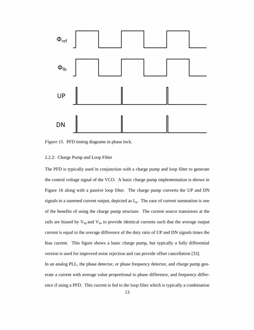
Figure 15. PFD timing diagrams in phase lock. ............................................................... 13
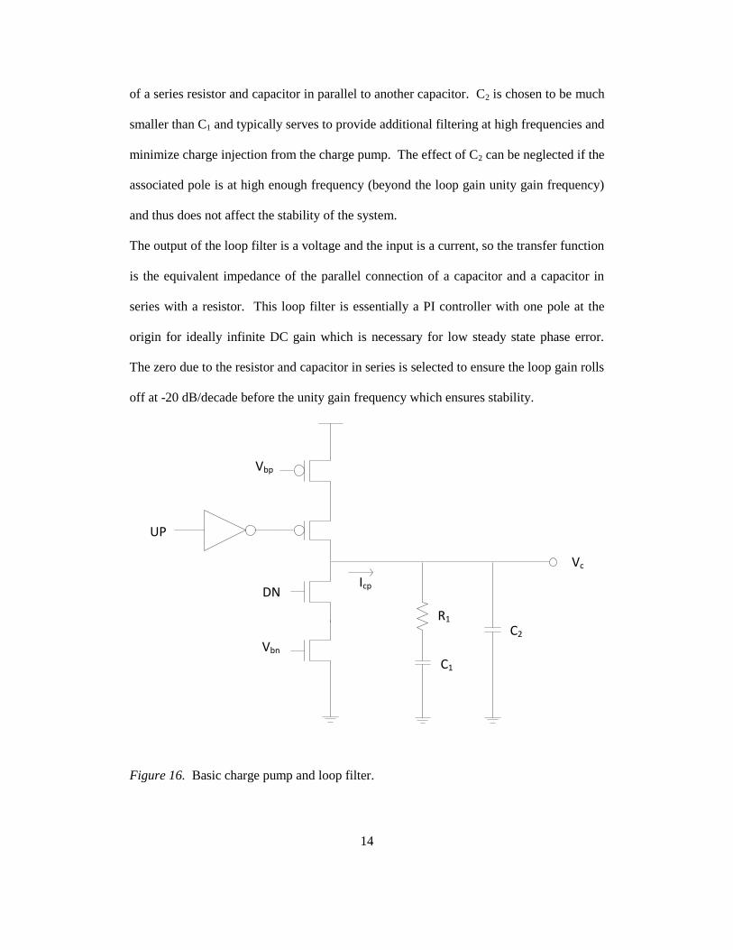
Figure 16. Basic charge pump and loop filter. ................................................................. 14
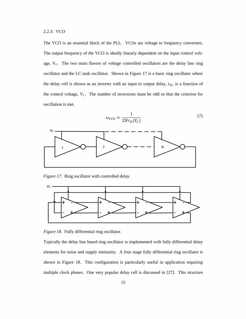
Figure 17. Ring oscillator with controlled delay. ............................................................. 15
Figure 18. Fully differential ring oscillator. ..................................................................... 15
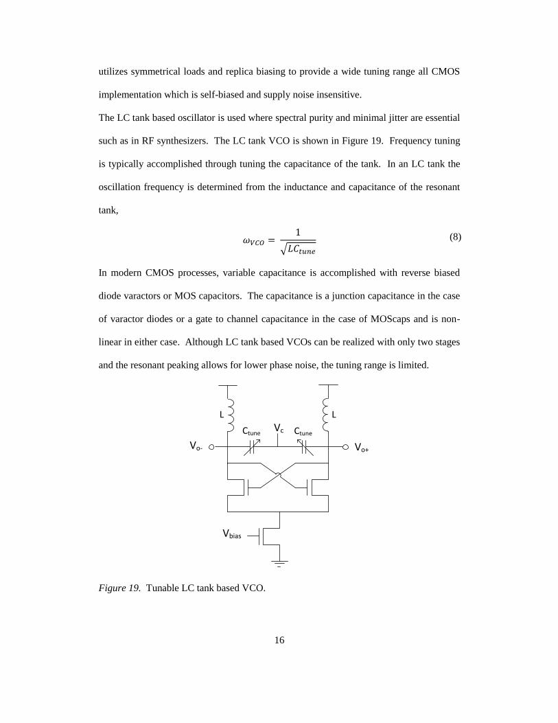
Figure 19. Tunable LC tank based VCO.......................................................................... 16
Figure 20. Frequency divider. .......................................................................................... 17
Figure 21. Programmable frequency divider. .................................................................. 18
vi
Figure Page
Figure 22. Timing jitter. ................................................................................................... 19
Figure 23. Simplified schematic of a charge pump PLL. ................................................ 20
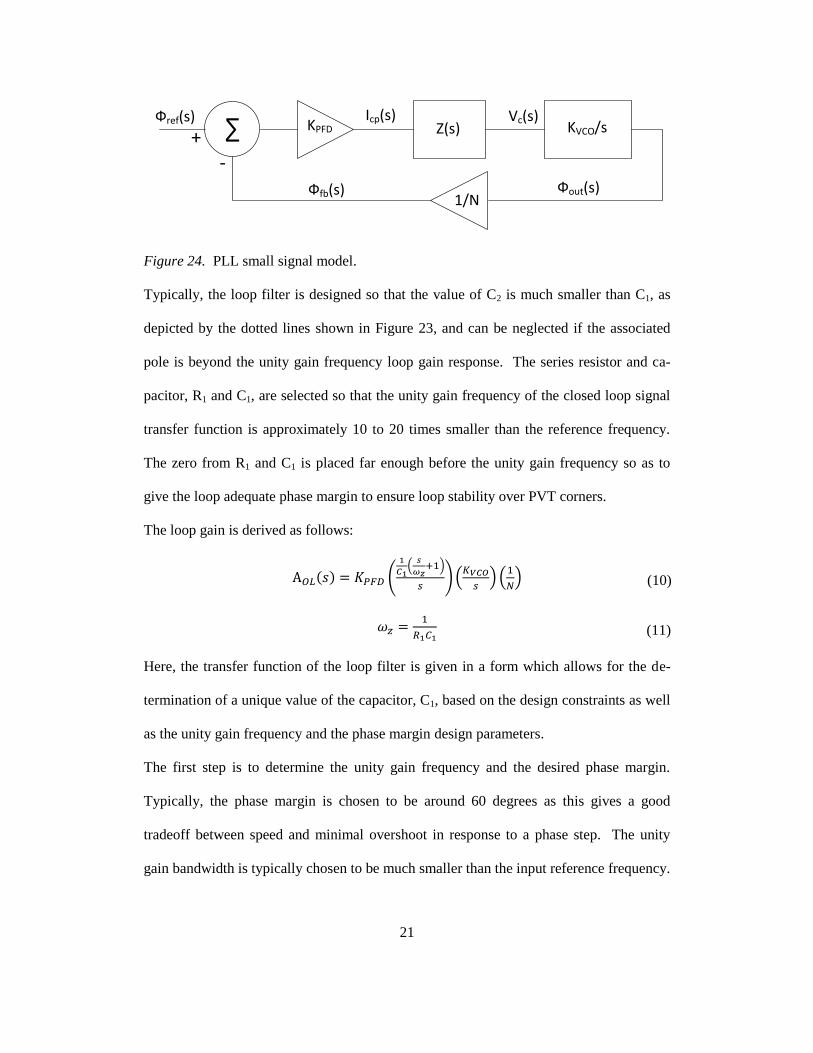
Figure 24. PLL small signal model. ................................................................................. 21
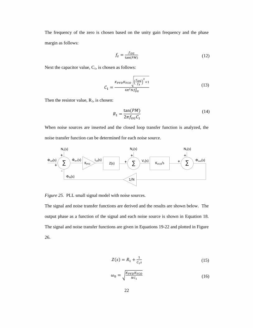
Figure 25. PLL small signal model with noise sources. .................................................. 22
Figure 26. 2nd
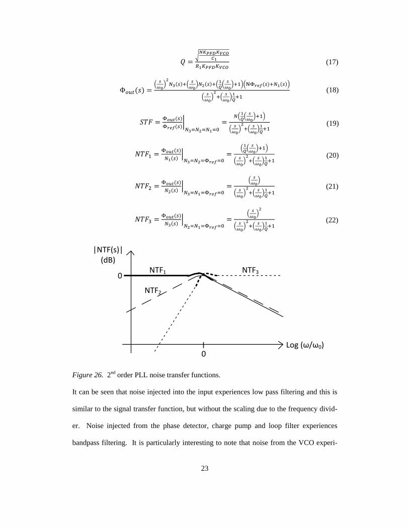
order PLL noise transfer functions. ........................................................... 23
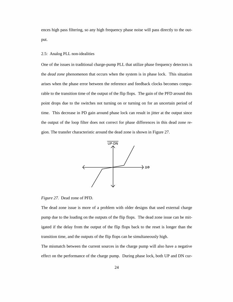
Figure 27. Dead zone of PFD. ......................................................................................... 24
Figure 28. Block diagram of ADPLL. ............................................................................. 26
Figure 29. Simple time to digital converter. .................................................................... 28
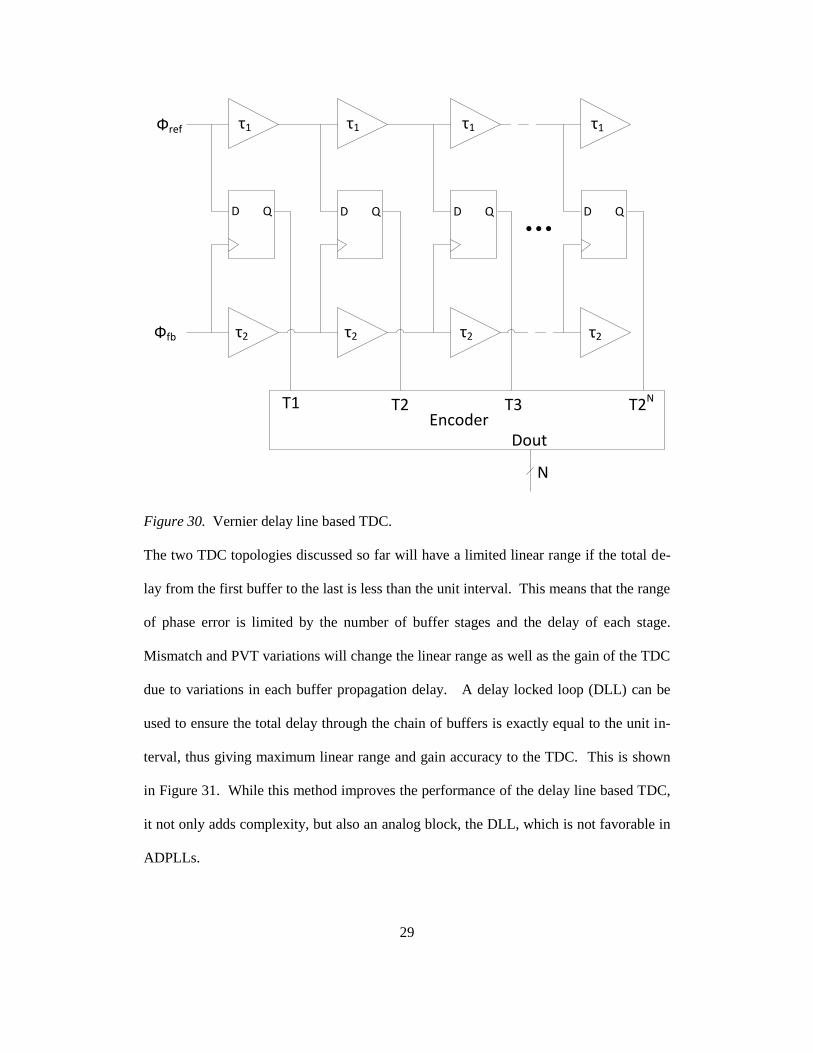
Figure 30. Vernier delay line based TDC. ....................................................................... 29
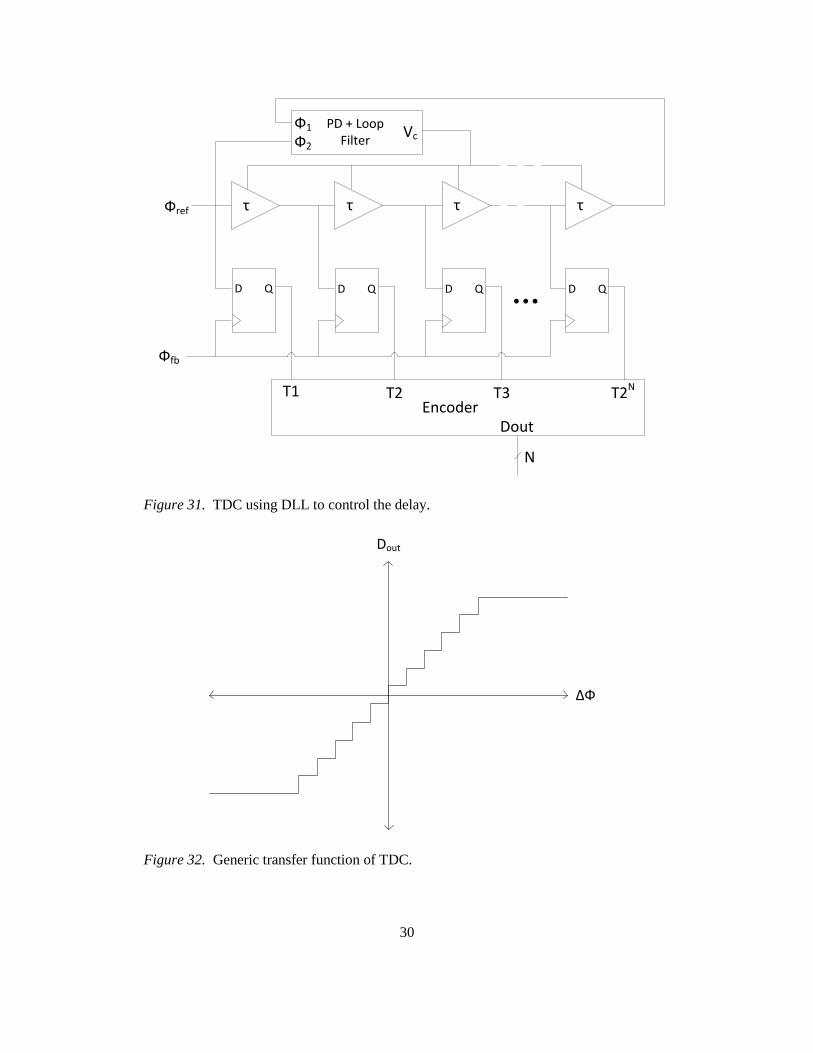
Figure 31. TDC using DLL to control the delay. ............................................................. 30
Figure 32. Generic transfer function of TDC. .................................................................. 30
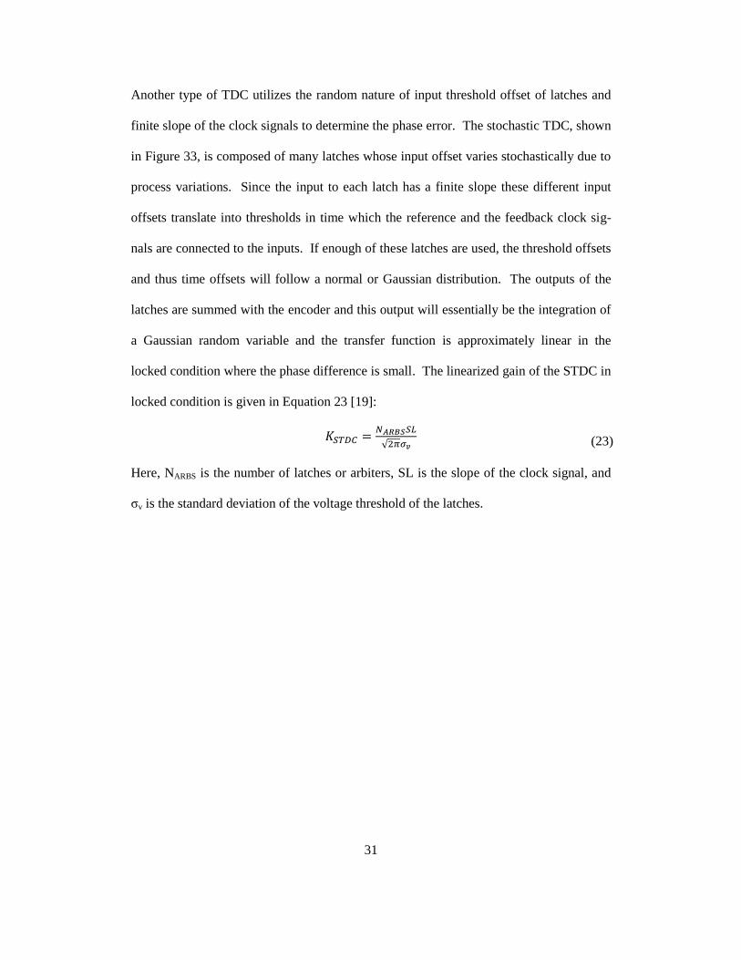
Figure 33. Stochastic TDC. .............................................................................................. 32
Figure 34. Stochastic TDC transfer characteristic. .......................................................... 32
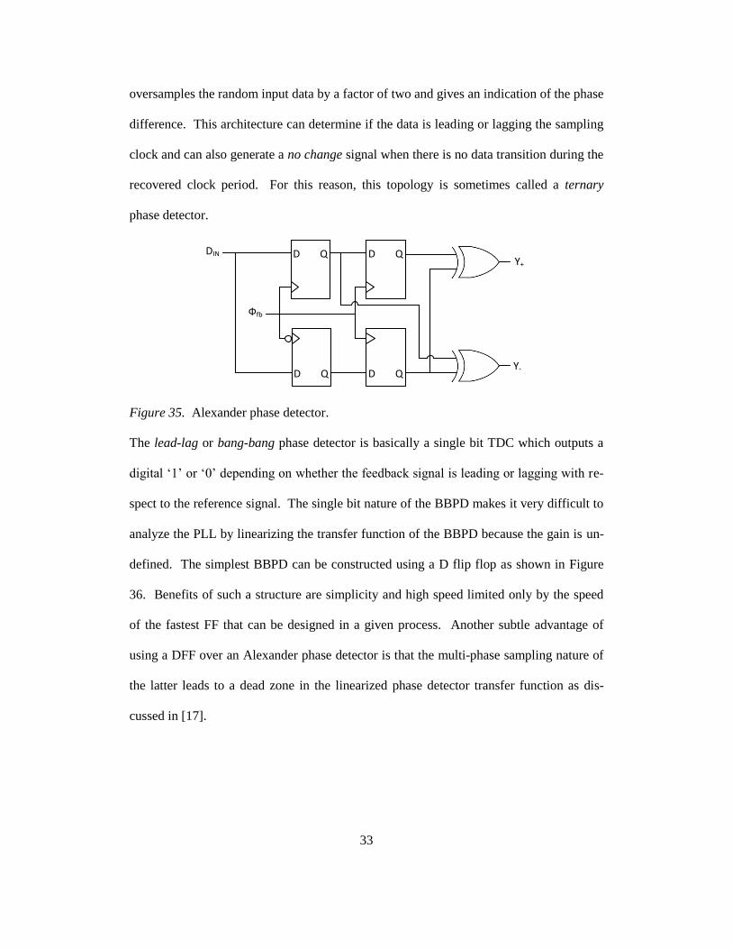
Figure 35. Alexander phase detector................................................................................ 33
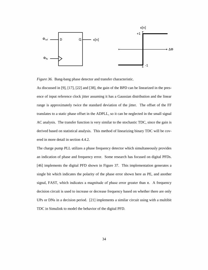
Figure 36. Bang-bang phase detector and transfer characteristic. ................................... 34
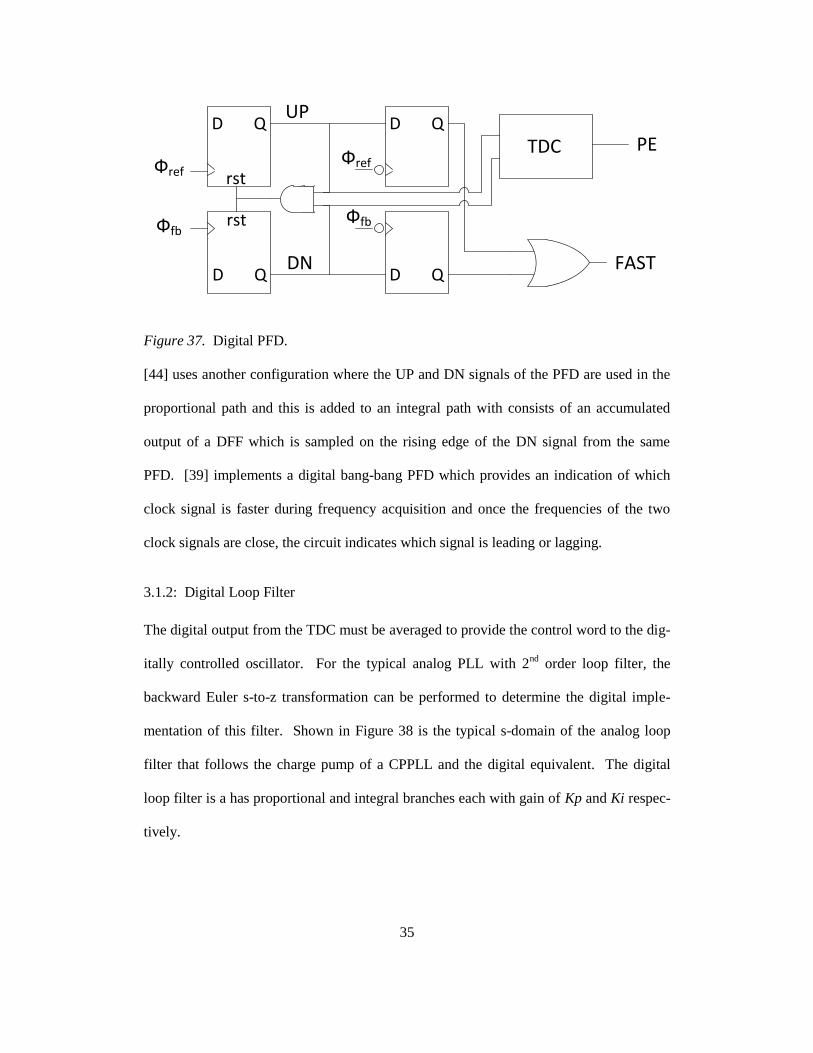
Figure 37. Digital PFD. .................................................................................................... 35
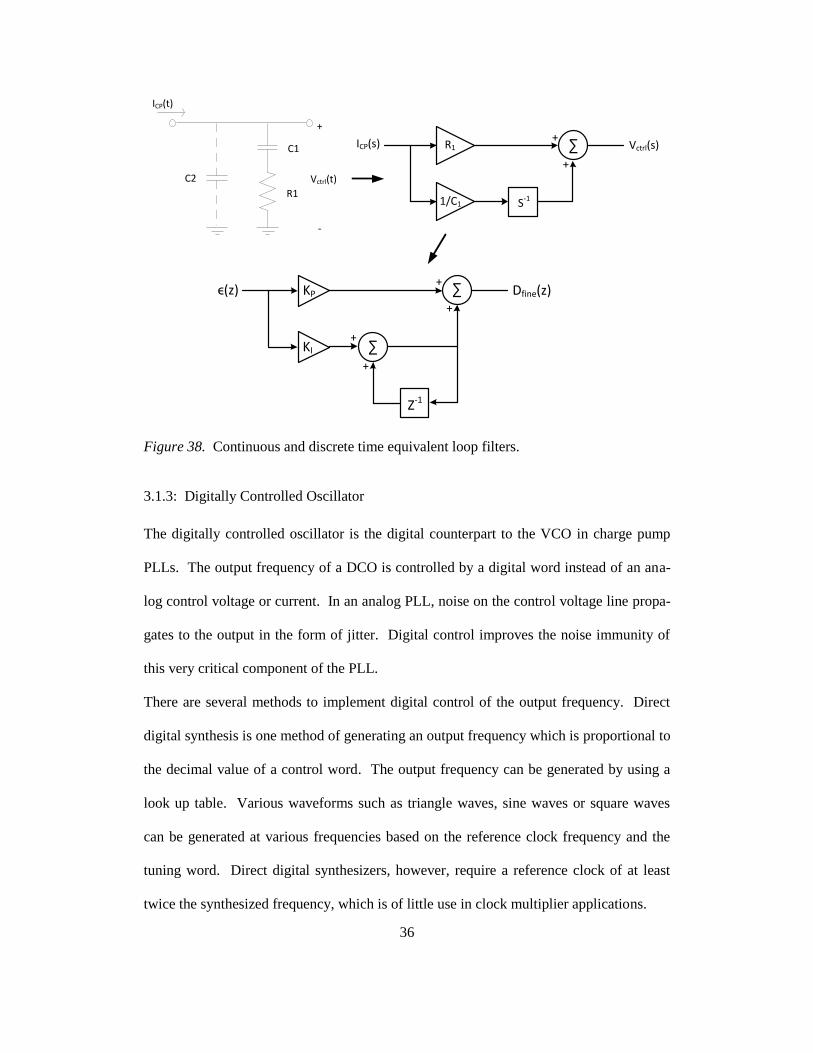
Figure 38. Continuous and discrete time equivalent loop filters. .................................... 36
Figure 39. Gated ring oscillator-based DCO. .................................................................. 37
Figure 40. LC tank-based DCO. ...................................................................................... 38
Figure 41. DAC and VCO-based DCO. ........................................................................... 38
Figure 42. Serializer top level. ......................................................................................... 44
Figure 43. 14 bit mux. ...................................................................................................... 45
Figure 44. ADPLL block diagram. .................................................................................. 46
Figure 45. Top level of ADPLL. ...................................................................................... 47
vii
Figure Page
Figure 46. Frequency divider. .......................................................................................... 48
Figure 47. Reset logic. ..................................................................................................... 48
Figure 48. Small signal model of 2nd
order PLL loop filter. ............................................ 50
Figure 49. Z-domain equivalent of 2nd
order PLL loop filter........................................... 50
Figure 50. Implementation of digital 2nd order PLL loop filter. ..................................... 51
Figure 51. Adder/subtractor. ............................................................................................ 52
Figure 52. Frequency control loop. .................................................................................. 53
Figure 53. Frequency detector. ........................................................................................ 54
Figure 54. 6-bit counter.................................................................................................... 54
Figure 55. Frequency control. .......................................................................................... 56
Figure 56. Lock detect logic. ........................................................................................... 56
Figure 57. DAC bias. ....................................................................................................... 58
Figure 58. Segmented current DAC top level. ................................................................. 59
Figure 59. 4 bit binary weighted DAC. ............................................................................ 59
Figure 60. 6 bit unary weighted (thermometer coded) DAC [30]. ................................... 60
Figure 61. Row and column decoders. ............................................................................. 60
Figure 62. Current controlled oscillator. .......................................................................... 62
Figure 63. ICO bias. ......................................................................................................... 62
Figure 64. DCO comparator. ........................................................................................... 63
Figure 65. Simplified block diagram of bang-bang ADPLL. .......................................... 64
Figure 66. Modeling BBPD using delta-sigma modulator approximation [40]. .............. 67
Figure 67. Non-linear small signal model of bang-bang ADPLL. ................................... 68
Figure 68. Linearized small signal model of bang-bang ADPLL. ................................... 68
Figure 69. Lock time for various start frequencies (behavioral DCO, Kp = 4, Ki =1). .... 74
viii
Figure Page
Figure 70. Lock time for various Kp (behavioral DCO, Ki=1). ........................................ 75
Figure 71. Transient with FLL and PLL (BSIM 3.3 DCO, Kp=8, Ki=1). ........................ 76
Figure 72. Transient with FLL and PLL zoomed (BSIM 3.3 DCO, Kp=8, Ki=1). .......... 77
Figure 73. Transient with FLL and PLL zoomed further (BSIM 3.3 DCO, Kp=8, Ki=1).
.......................................................................................................................................... 77
Figure 74. Step response (Behavioral DCO, Kp=8, Ki=1). .............................................. 78
Figure 75. Step response without reference (Behavioral DCO, Kp=8, Ki=1). ................. 79
Figure 76. Transient without DLL (BSIM 3.3 DCO, Kp=8, Ki=1). ................................. 80
Figure 77. Persistence plot without DLL (BSIM 3.3 DCO, Kp=8, Ki=1). ....................... 80
Figure 78. Transient without DLL (BSIM 3.3 DCO, Kp=4, Ki=1). ................................. 81
Figure 79. Persistence plot without DLL (BSIM 3.3 DCO, Kp=4, Ki=1). ...................... 82
Figure 80. Transient without DLL with 20 mVpp, 1 MHz supply noise (BSIM 3.3 DCO,
Kp=4, Ki=1). ..................................................................................................................... 83
Figure 81. Persistence plot without DLL with 20 mVpp, 1 MHz supply noise (BSIM 3.3
DCO, Kp=4, Ki=1). .......................................................................................................... 84
Figure 82. Frequency step response (BSIM 3.3 DCO, Kp=4, Ki=1, ‘nom’). .................. 85
Figure 83. Frequency step response (BSIM 3.3 DCO, Kp=4, Ki=1, ‘nom’). .................. 85
Figure 84. Frequency step response (BSIM 3.3 DCO, Kp=4, Ki=1, ‘fast’). ................... 86
Figure 85. Frequency step response (BSIM 3.3 DCO, Kp=4, Ki=1, ‘fast’). ................... 86
Figure 86. Frequency step response (BSIM 3.3 DCO, Kp=4, Ki=1, ‘slow’). .................. 87
Figure 87. Frequency step response (BSIM 3.3 DCO, Kp=4, Ki=1, ‘slow’). .................. 87
Figure 88. Frequency step response (BSIM 3.3 DCO, Kp=4, Ki=1, ‘room temp’). ........ 88
Figure 89. Frequency step response (BSIM 3.3 DCO, Kp=4, Ki=1, ‘room temp’). ........ 88
Figure 90. Phase step response (BSIM 3.3 DCO, Kp=4, Ki=1, ‘nom’)........................... 89
ix
Figure Page
Figure 91. Phase step response (BSIM 3.3 DCO, Kp=4, Ki=1, ‘fast’). ........................... 90
Figure 92. Phase step response (BSIM 3.3 DCO, Kp=4, Ki=1, ‘slow’). ......................... 90
Figure 93. Phase step response (BSIM 3.3 DCO, Kp=4, Ki=1, ‘room temp’). ............... 91
Figure 94. Evaluation board setup. .................................................................................. 95
1
Chapter 1: INTRODUCTION
1.1: Motivation
Phase locked loops (PLLs) are critical components to any digital or mixed-signal system
that requires an accurate clock signal. PLLs find applications in communications, wire-
less transceivers, data converters and other mixed signal systems. Two particular appli-
cations of PLLs are data recovery circuits and frequency synthesis. In clock and data
recovery circuits used in high-speed I/O systems, the PLL can be used to recover the
clock signal embedded in a serial data stream and capture the data using this recovered
clock signal to sample the data optimally to minimize error in data transmission. In wire-
less transceivers which require a local oscillator signal which is some multiple of a stable
crystal oscillator frequency, the PLL is used for frequency synthesis and facilitates mix-
ing for baseband processing or high frequency transmission. Other uses of PLLs are
clock generation and distribution, jitter filtering, and clock skew removal.
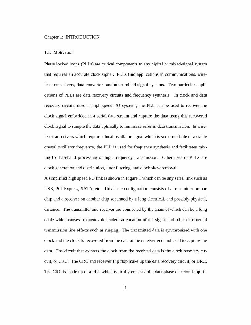
A simplified high speed I/O link is shown in Figure 1 which can be any serial link such as
USB, PCI Express, SATA, etc. This basic configuration consists of a transmitter on one
chip and a receiver on another chip separated by a long electrical, and possibly physical,
distance. The transmitter and receiver are connected by the channel which can be a long
cable which causes frequency dependent attenuation of the signal and other detrimental
transmission line effects such as ringing. The transmitted data is synchronized with one
clock and the clock is recovered from the data at the receiver end and used to capture the
data. The circuit that extracts the clock from the received data is the clock recovery cir-
cuit, or CRC. The CRC and receiver flip flop make up the data recovery circuit, or DRC.
The CRC is made up of a PLL which typically consists of a data phase detector, loop fil-
2
ter and VCO. The clock generated by the CRC sample the received data such that the bit
error rate can be minimized.
Oscillator
D QDIN
CRC
DOUTD QChannelDriver Amp
Figure 1. Clock recovery application of PLLs.
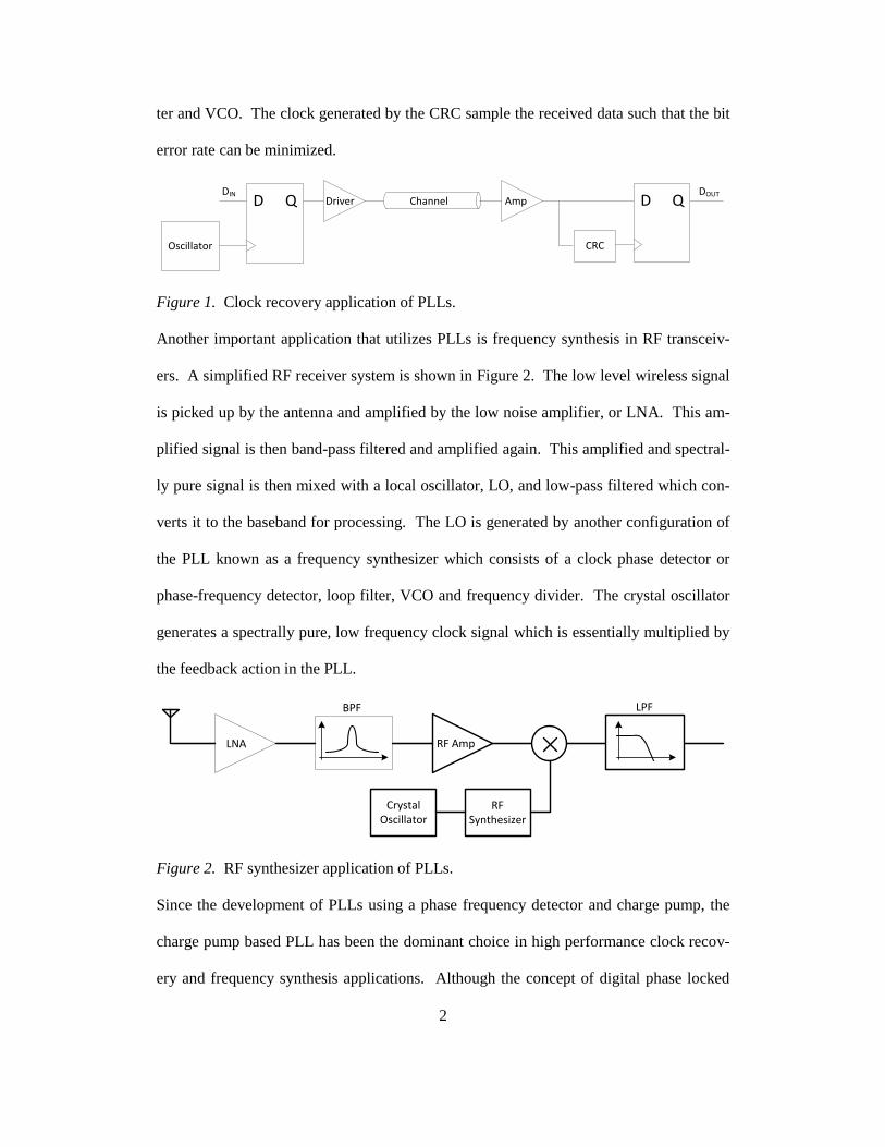
Another important application that utilizes PLLs is frequency synthesis in RF transceiv-
ers. A simplified RF receiver system is shown in Figure 2. The low level wireless signal
is picked up by the antenna and amplified by the low noise amplifier, or LNA. This am-
plified signal is then band-pass filtered and amplified again. This amplified and spectral-
ly pure signal is then mixed with a local oscillator, LO, and low-pass filtered which con-
verts it to the baseband for processing. The LO is generated by another configuration of
the PLL known as a frequency synthesizer which consists of a clock phase detector or
phase-frequency detector, loop filter, VCO and frequency divider. The crystal oscillator
generates a spectrally pure, low frequency clock signal which is essentially multiplied by
the feedback action in the PLL.
LNA RF Amp
RF Synthesizer
Crystal Oscillator
BPF LPF
Figure 2. RF synthesizer application of PLLs.
Since the development of PLLs using a phase frequency detector and charge pump, the
charge pump based PLL has been the dominant choice in high performance clock recov-
ery and frequency synthesis applications. Although the concept of digital phase locked
3
loops has been around since the 1970’s [15], it is only within the last decade that all-
digital PLLs have gained much attention from researchers. As process geometries con-
tinue to scale down and more systems are being integrated on a single chip, sensitive ana-
log circuitry is being surrounded by more and more noisy digital circuitry. This is espe-
cially true in wireless communication SoCs. Since analog circuitry does not scale as well
as digital, it has become necessary to limit analog circuitry wherever possible, including
PLLs.
All-digital implementations of PLLs are necessary to reduce the sensitivity to process,
voltage and temperature (PVT) variations as well as minimize circuit area, power and
noise susceptibility. Loop filter capacitor leakage and design portability are other very
important reasons for going digital. The goal of this thesis is to explore the current state
of the art in ADPLLs and implement a high performance, low power, highly integrated
ADPLL in a 180 nm CMOS process.
1.2: Thesis Organization
Chapter 2 introduces the basic concept of phase locking and discusses different imple-
mentations of analog phase locked loops with emphasis on the charge pump based PLL.
The various building blocks and implementations as well as modeling of these blocks and
the system are examined. Chapter 3 introduces the all-digital PLL and surveys different
implementations and discusses the state of the art of these systems. Chapter 4 discusses
an application of an all-digital PLL and covers its specification, design and circuit im-
plementation. Chapter 5 examines the simulation results and Chapter 6 concludes the
work.
4
Chapter 2: CHARGE PUMP PLL
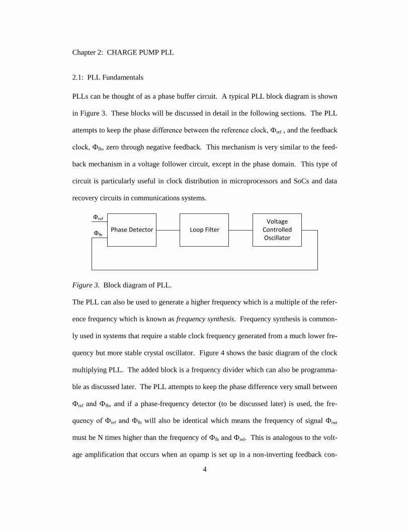
2.1: PLL Fundamentals
PLLs can be thought of as a phase buffer circuit. A typical PLL block diagram is shown
in Figure 3. These blocks will be discussed in detail in the following sections. The PLL
attempts to keep the phase difference between the reference clock, Фref , and the feedback
clock, Фfb, zero through negative feedback. This mechanism is very similar to the feed-
back mechanism in a voltage follower circuit, except in the phase domain. This type of
circuit is particularly useful in clock distribution in microprocessors and SoCs and data
recovery circuits in communications systems.
Phase Detector Loop FilterVoltage
Controlled Oscillator
Фref
Фfb
Figure 3. Block diagram of PLL.
The PLL can also be used to generate a higher frequency which is a multiple of the refer-
ence frequency which is known as frequency synthesis. Frequency synthesis is common-
ly used in systems that require a stable clock frequency generated from a much lower fre-
quency but more stable crystal oscillator. Figure 4 shows the basic diagram of the clock
multiplying PLL. The added block is a frequency divider which can also be programma-
ble as discussed later. The PLL attempts to keep the phase difference very small between
Фref and Фfb, and if a phase-frequency detector (to be discussed later) is used, the fre-
quency of Фref and Фfb will also be identical which means the frequency of signal Фout
must be N times higher than the frequency of Фfb and Фref. This is analogous to the volt-
age amplification that occurs when an opamp is set up in a non-inverting feedback con-
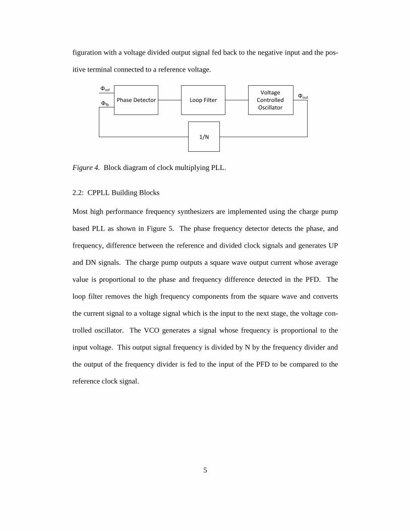
5
figuration with a voltage divided output signal fed back to the negative input and the pos-
itive terminal connected to a reference voltage.
Phase Detector Loop FilterVoltage
Controlled Oscillator
Фref
Фfb
Фout
1/N
Figure 4. Block diagram of clock multiplying PLL.
2.2: CPPLL Building Blocks
Most high performance frequency synthesizers are implemented using the charge pump
based PLL as shown in Figure 5. The phase frequency detector detects the phase, and
frequency, difference between the reference and divided clock signals and generates UP
and DN signals. The charge pump outputs a square wave output current whose average
value is proportional to the phase and frequency difference detected in the PFD. The
loop filter removes the high frequency components from the square wave and converts
the current signal to a voltage signal which is the input to the next stage, the voltage con-
trolled oscillator. The VCO generates a signal whose frequency is proportional to the
input voltage. This output signal frequency is divided by N by the frequency divider and
the output of the frequency divider is fed to the input of the PFD to be compared to the
reference clock signal.
6
(4)
Phase Frequency Detector
Loop FilterVoltage
Controlled Oscillator
Фref
Фfb
ФoutCharge Pump
UP
DN
1/N
ICP VC
Figure 5. Charge pump PLL.
2.2.1: Phase Detector
The phase detector is a circuit that generates an output signal whose average value is lin-
early related to the difference in phase of the reference clock and the divided clock sig-
nals. This relationship can be described by the equation,
( )
In this equation, is the average value of the output signal in a given period and
can be a voltage, current or charge depending on the particular implementation.
Phase detection can be accomplished in a number of ways. Early on, phase detection was
accomplished through analog multiplication. In general, if Vin1 and Vin2 are sinusoidal
signals at frequencies of ω1 and ω2, with phases Ф1 and Ф2, then the product signal will
contain terms which are sums and differences of the total phase of each signal.
If , Equation 4 simplifies to
(1)
(2)
(3)
(5)
7
The average or DC term is proportional to . While this method does in
fact produce an output with a DC value dependent on the phase difference of the input
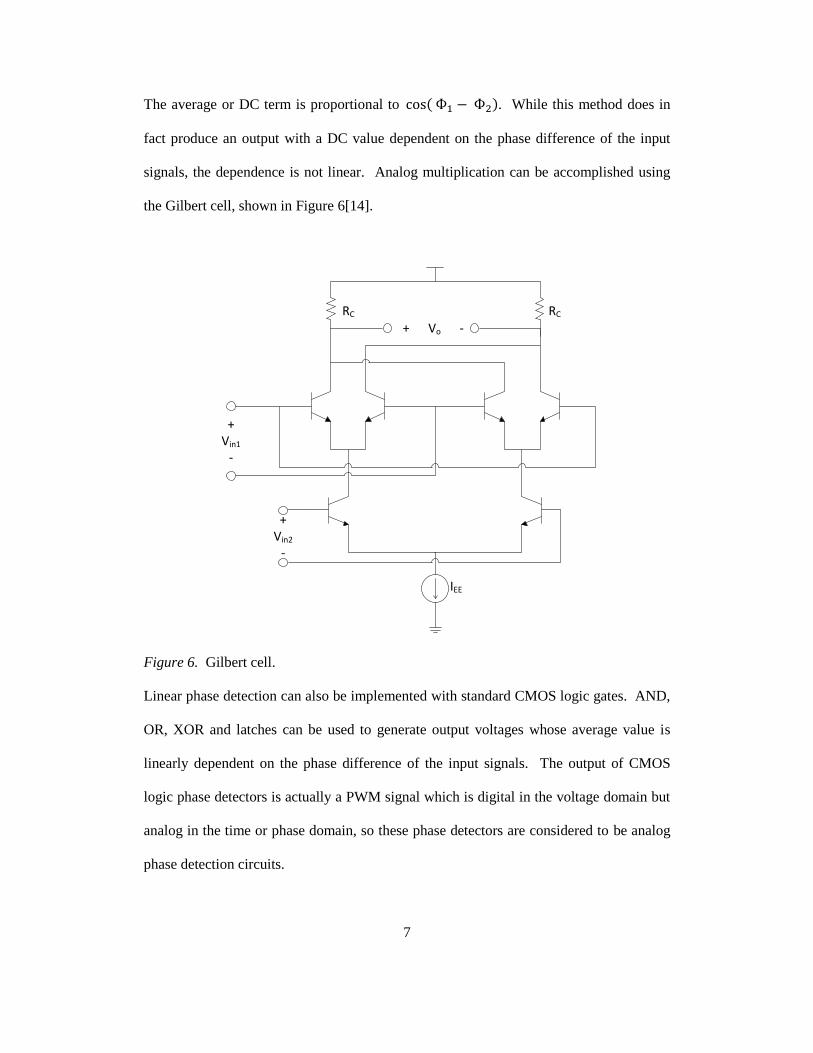
signals, the dependence is not linear. Analog multiplication can be accomplished using
the Gilbert cell, shown in Figure 6[14].
IEE
+Vin1
-
+Vin2
-
+ Vo -
RC RC
Figure 6. Gilbert cell.
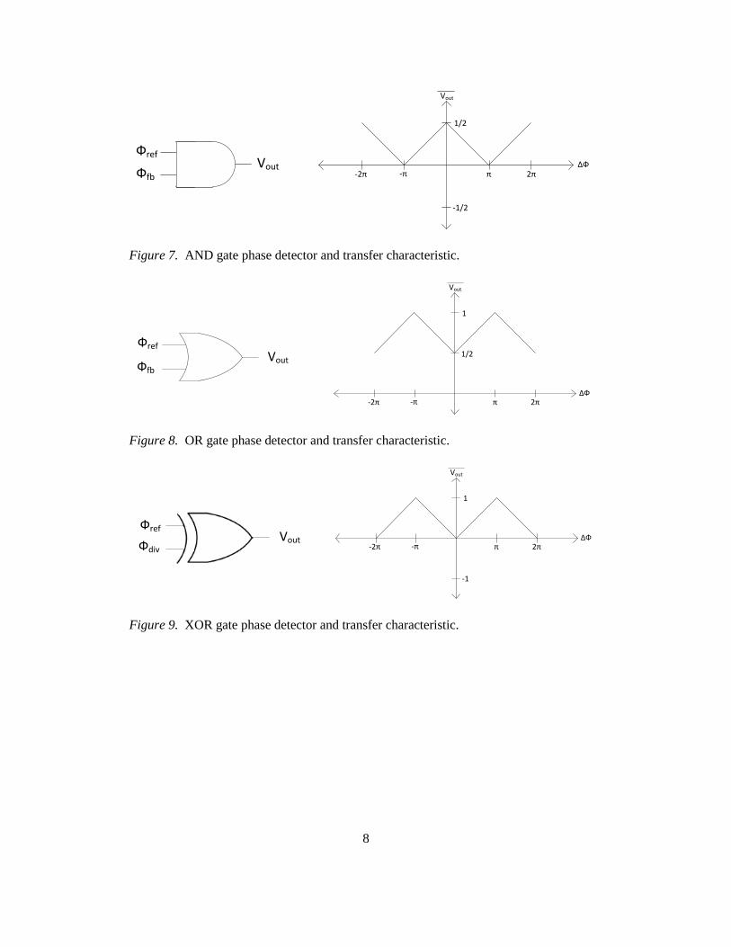
Linear phase detection can also be implemented with standard CMOS logic gates. AND,
OR, XOR and latches can be used to generate output voltages whose average value is
linearly dependent on the phase difference of the input signals. The output of CMOS
logic phase detectors is actually a PWM signal which is digital in the voltage domain but
analog in the time or phase domain, so these phase detectors are considered to be analog
phase detection circuits.
8
Фref
Фfb Vout ∆Ф
Vout
π 2π -2π -π
1/2
-1/2
Figure 7. AND gate phase detector and transfer characteristic.
Фref
Фfb Vout
∆Ф
Vout
π 2π -2π -π
1
1/2
Figure 8. OR gate phase detector and transfer characteristic.
Vout ∆Ф
Vout
π 2π -2π -π
1
-1
Фref
Фdiv
Figure 9. XOR gate phase detector and transfer characteristic.
9
Фref
Фfb
∆Ф↔
VOUT,AND
VOUT,OR
VOUT,XOR
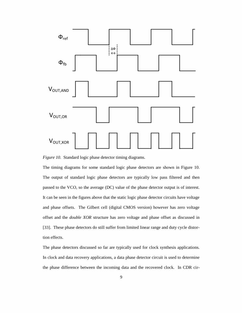
Figure 10. Standard logic phase detector timing diagrams.
The timing diagrams for some standard logic phase detectors are shown in Figure 10.
The output of standard logic phase detectors are typically low pass filtered and then
passed to the VCO, so the average (DC) value of the phase detector output is of interest.
It can be seen in the figures above that the static logic phase detector circuits have voltage
and phase offsets. The Gilbert cell (digital CMOS version) however has zero voltage
offset and the double XOR structure has zero voltage and phase offset as discussed in
[33]. These phase detectors do still suffer from limited linear range and duty cycle distor-
tion effects.
The phase detectors discussed so far are typically used for clock synthesis applications.
In clock and data recovery applications, a data phase detector circuit is used to determine
the phase difference between the incoming data and the recovered clock. In CDR cir-
10
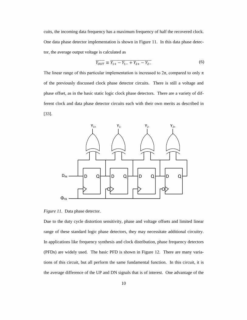
cuits, the incoming data frequency has a maximum frequency of half the recovered clock.
One data phase detector implementation is shown in Figure 11. In this data phase detec-
tor, the average output voltage is calculated as
The linear range of this particular implementation is increased to 2π, compared to only π
of the previously discussed clock phase detector circuits. There is still a voltage and
phase offset, as in the basic static logic clock phase detectors. There are a variety of dif-
ferent clock and data phase detector circuits each with their own merits as described in
[33].
D QDIN
ΦFB
D Q D Q D Q
Y1+ Y1- Y2- Y2+
Figure 11. Data phase detector.
Due to the duty cycle distortion sensitivity, phase and voltage offsets and limited linear
range of these standard logic phase detectors, they may necessitate additional circuitry.
In applications like frequency synthesis and clock distribution, phase frequency detectors
(PFDs) are widely used. The basic PFD is shown in Figure 12. There are many varia-
tions of this circuit, but all perform the same fundamental function. In this circuit, it is
the average difference of the UP and DN signals that is of interest. One advantage of the
(6)
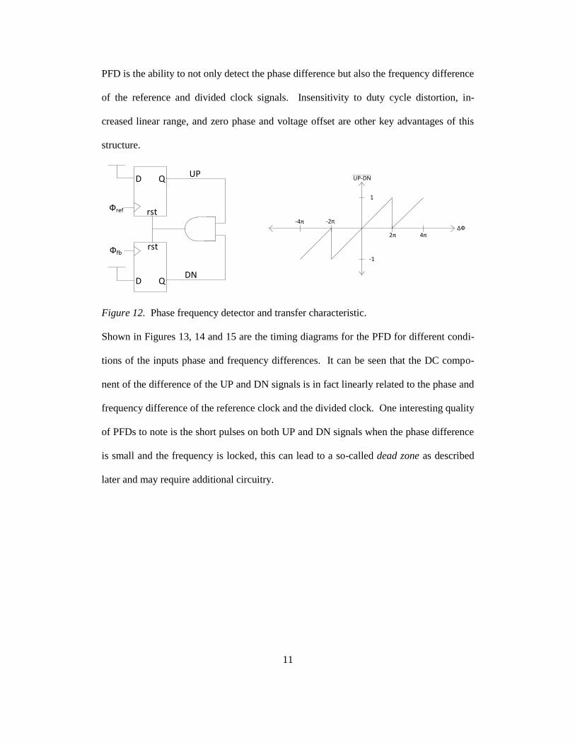
11
PFD is the ability to not only detect the phase difference but also the frequency difference
of the reference and divided clock signals. Insensitivity to duty cycle distortion, in-
creased linear range, and zero phase and voltage offset are other key advantages of this
structure.
Фref
Фfb
D Q
rst
D Q
rst
UP
DN
∆Ф
UP-DN
2π 4π
-4π -2π
1
-1
Figure 12. Phase frequency detector and transfer characteristic.
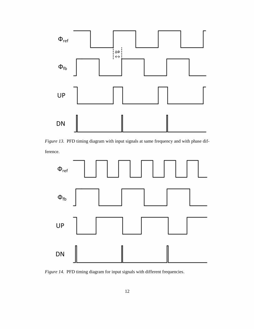
Shown in Figures 13, 14 and 15 are the timing diagrams for the PFD for different condi-
tions of the inputs phase and frequency differences. It can be seen that the DC compo-
nent of the difference of the UP and DN signals is in fact linearly related to the phase and
frequency difference of the reference clock and the divided clock. One interesting quality
of PFDs to note is the short pulses on both UP and DN signals when the phase difference
is small and the frequency is locked, this can lead to a so-called dead zone as described
later and may require additional circuitry.
12
Фref
Фfb
∆Ф↔
UP
DN
Figure 13. PFD timing diagram with input signals at same frequency and with phase dif-
ference.
Фref
Фfb
UP
DN
Figure 14. PFD timing diagram for input signals with different frequencies.
13
Фref
Фfb
UP
DN
Figure 15. PFD timing diagrams in phase lock.
2.2.2: Charge Pump and Loop Filter
The PFD is typically used in conjunction with a charge pump and loop filter to generate
the control voltage signal of the VCO. A basic charge pump implementation is shown in
Figure 16 along with a passive loop filter. The charge pump converts the UP and DN
signals to a summed current output, depicted as Icp. The ease of current summation is one
of the benefits of using the charge pump structure. The current source transistors at the
rails are biased by Vbp and Vbn to provide identical currents such that the average output
current is equal to the average difference of the duty ratio of UP and DN signals times the
bias current. This figure shows a basic charge pump, but typically a fully differential
version is used for improved noise rejection and can provide offset cancellation [33].
In an analog PLL, the phase detector, or phase frequency detector, and charge pump gen-
erate a current with average value proportional to phase difference, and frequency differ-
ence if using a PFD. This current is fed to the loop filter which is typically a combination
14
of a series resistor and capacitor in parallel to another capacitor. C2 is chosen to be much
smaller than C1 and typically serves to provide additional filtering at high frequencies and
minimize charge injection from the charge pump. The effect of C2 can be neglected if the
associated pole is at high enough frequency (beyond the loop gain unity gain frequency)
and thus does not affect the stability of the system.
The output of the loop filter is a voltage and the input is a current, so the transfer function
is the equivalent impedance of the parallel connection of a capacitor and a capacitor in
series with a resistor. This loop filter is essentially a PI controller with one pole at the
origin for ideally infinite DC gain which is necessary for low steady state phase error.
The zero due to the resistor and capacitor in series is selected to ensure the loop gain rolls
off at -20 dB/decade before the unity gain frequency which ensures stability.
Vbn
Vbp
UP
DNIcp
Vc
C2
C1
R1
Figure 16. Basic charge pump and loop filter.
15
2.2.3: VCO
The VCO is an essential block of the PLL. VCOs are voltage to frequency converters.
The output frequency of the VCO is ideally linearly dependent on the input control volt-
age, VC. The two main flavors of voltage controlled oscillators are the delay line ring
oscillator and the LC tank oscillator. Shown in Figure 17 is a basic ring oscillator where
the delay cell is shown as an inverter with an input to output delay, , is a function of
the control voltage, VC. The number of inversions must be odd so that the criterion for
oscillation is met.
1 2 N
Vc
Figure 17. Ring oscillator with controlled delay.
Vc
+
- +
- +
- +
- +
- +
- +
- +
-
Figure 18. Fully differential ring oscillator.
Typically the delay line based ring oscillator is implemented with fully differential delay
elements for noise and supply immunity. A four stage fully differential ring oscillator is
shown in Figure 18. This configuration is particularly useful in application requiring
multiple clock phases. One very popular delay cell is discussed in [27]. This structure
(7)
16
utilizes symmetrical loads and replica biasing to provide a wide tuning range all CMOS
implementation which is self-biased and supply noise insensitive.
The LC tank based oscillator is used where spectral purity and minimal jitter are essential
such as in RF synthesizers. The LC tank VCO is shown in Figure 19. Frequency tuning
is typically accomplished through tuning the capacitance of the tank. In an LC tank the
oscillation frequency is determined from the inductance and capacitance of the resonant
tank,
√
In modern CMOS processes, variable capacitance is accomplished with reverse biased
diode varactors or MOS capacitors. The capacitance is a junction capacitance in the case
of varactor diodes or a gate to channel capacitance in the case of MOScaps and is non-
linear in either case. Although LC tank based VCOs can be realized with only two stages
and the resonant peaking allows for lower phase noise, the tuning range is limited.
Vo+Vo-
Vc
Vbias
LL
Ctune Ctune
Figure 19. Tunable LC tank based VCO.
(8)
17
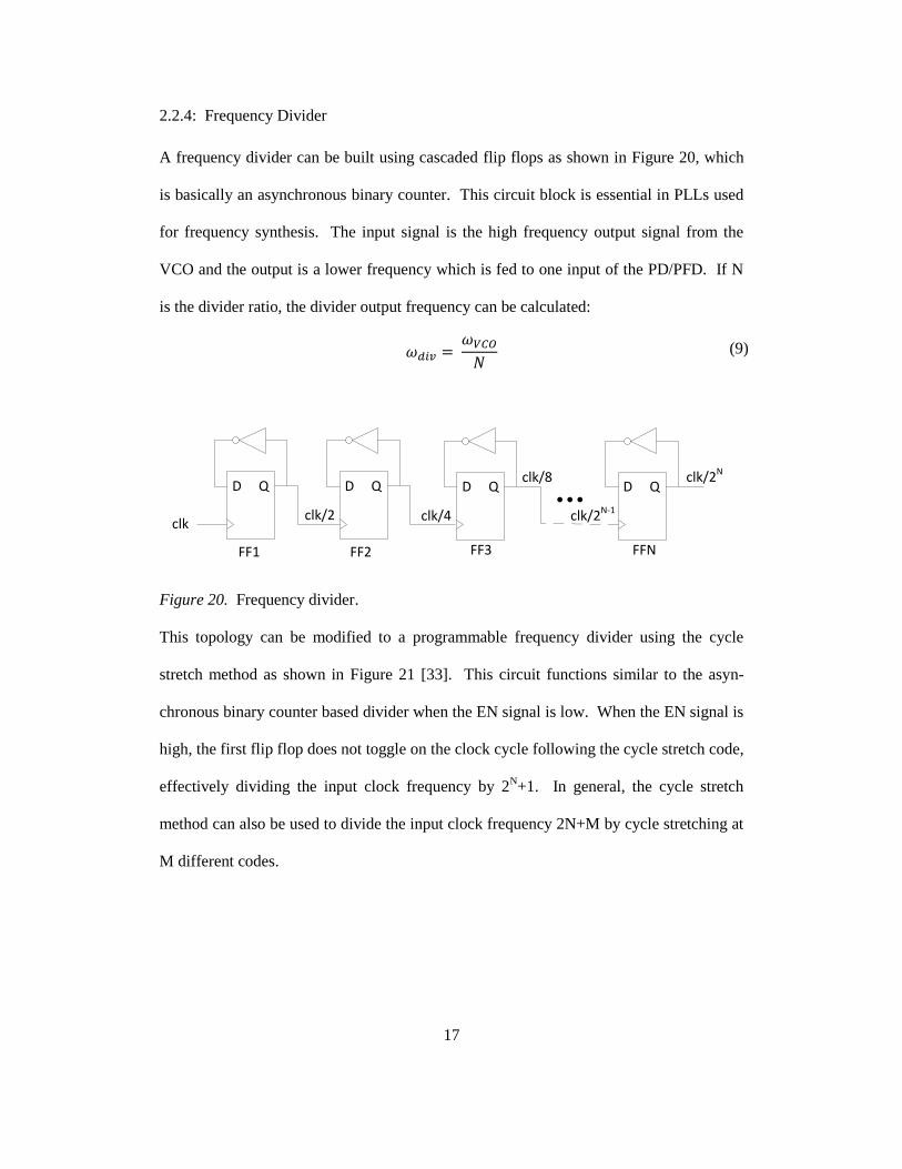
2.2.4: Frequency Divider
A frequency divider can be built using cascaded flip flops as shown in Figure 20, which
is basically an asynchronous binary counter. This circuit block is essential in PLLs used
for frequency synthesis. The input signal is the high frequency output signal from the
VCO and the output is a lower frequency which is fed to one input of the PD/PFD. If N
is the divider ratio, the divider output frequency can be calculated:
D Q D Q D Q D Q
clkclk/2 clk/4
clk/8
clk/2N-1
clk/2N
FF1 FF2 FF3 FFN
Figure 20. Frequency divider.
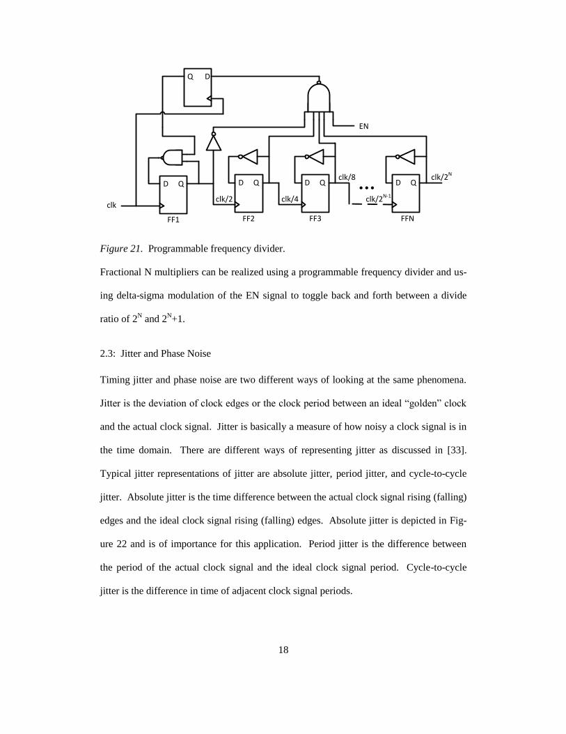
This topology can be modified to a programmable frequency divider using the cycle
stretch method as shown in Figure 21 [33]. This circuit functions similar to the asyn-
chronous binary counter based divider when the EN signal is low. When the EN signal is
high, the first flip flop does not toggle on the clock cycle following the cycle stretch code,
effectively dividing the input clock frequency by 2N+1. In general, the cycle stretch
method can also be used to divide the input clock frequency 2N+M by cycle stretching at
M different codes.
(9)
18
D Q D Q D Q D Q
clkclk/4
clk/8
clk/2N-1
clk/2N
FF1 FF2 FF3 FFN
DQ
clk/2
EN
Figure 21. Programmable frequency divider.
Fractional N multipliers can be realized using a programmable frequency divider and us-
ing delta-sigma modulation of the EN signal to toggle back and forth between a divide
ratio of 2N and 2
N+1.
2.3: Jitter and Phase Noise
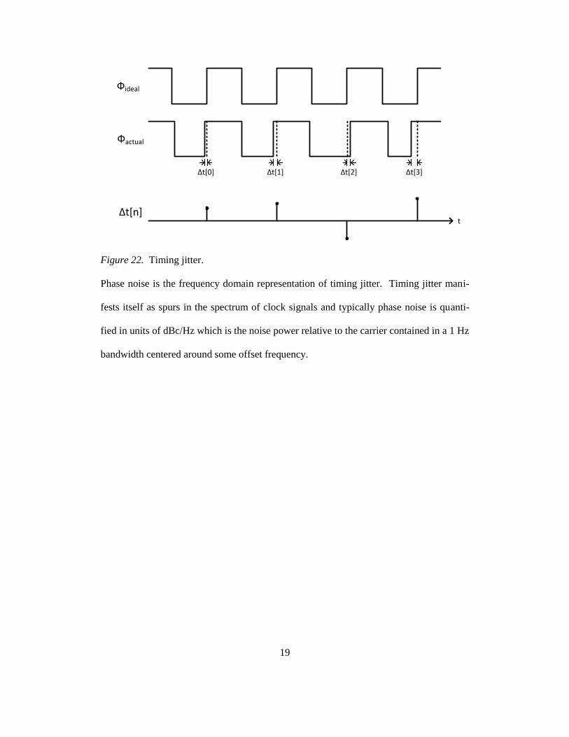
Timing jitter and phase noise are two different ways of looking at the same phenomena.
Jitter is the deviation of clock edges or the clock period between an ideal “golden” clock
and the actual clock signal. Jitter is basically a measure of how noisy a clock signal is in
the time domain. There are different ways of representing jitter as discussed in [33].
Typical jitter representations of jitter are absolute jitter, period jitter, and cycle-to-cycle
jitter. Absolute jitter is the time difference between the actual clock signal rising (falling)
edges and the ideal clock signal rising (falling) edges. Absolute jitter is depicted in Fig-
ure 22 and is of importance for this application. Period jitter is the difference between
the period of the actual clock signal and the ideal clock signal period. Cycle-to-cycle
jitter is the difference in time of adjacent clock signal periods.
19
Фactual
∆t[1]∆t[0] ∆t[2] ∆t[3]
Фideal
∆t[n]t
Figure 22. Timing jitter.
Phase noise is the frequency domain representation of timing jitter. Timing jitter mani-
fests itself as spurs in the spectrum of clock signals and typically phase noise is quanti-
fied in units of dBc/Hz which is the noise power relative to the carrier contained in a 1 Hz
bandwidth centered around some offset frequency.
20
2.4: Analysis and Parameter Selection
2.4.1: Small Signal Analysis for 2nd
Order Analog PLLs
Фref
Фfb
D Q
rst
D Q
rst
UP
DN Icp
Vc
C2
C1
R1
DQDQDQDQ
clkclk/2clk/4
clk/8
clk/2N-1
clk/2N
FF1FF2FF3FFN
τ τ τ
IB
IB
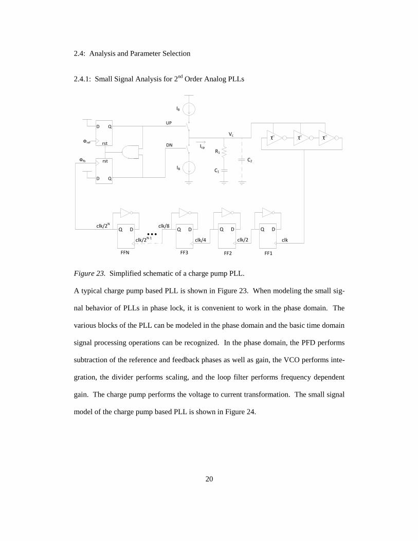
Figure 23. Simplified schematic of a charge pump PLL.
A typical charge pump based PLL is shown in Figure 23. When modeling the small sig-
nal behavior of PLLs in phase lock, it is convenient to work in the phase domain. The
various blocks of the PLL can be modeled in the phase domain and the basic time domain
signal processing operations can be recognized. In the phase domain, the PFD performs
subtraction of the reference and feedback phases as well as gain, the VCO performs inte-
gration, the divider performs scaling, and the loop filter performs frequency dependent
gain. The charge pump performs the voltage to current transformation. The small signal
model of the charge pump based PLL is shown in Figure 24.
21
Фref(s)
Фfb(s) Фout(s)
Icp(s) Vc(s)KPFD
1/N
KVCO/sZ(s)+
-
∑
Figure 24. PLL small signal model.
Typically, the loop filter is designed so that the value of C2 is much smaller than C1, as
depicted by the dotted lines shown in Figure 23, and can be neglected if the associated
pole is beyond the unity gain frequency loop gain response. The series resistor and ca-
pacitor, R1 and C1, are selected so that the unity gain frequency of the closed loop signal
transfer function is approximately 10 to 20 times smaller than the reference frequency.
The zero from R1 and C1 is placed far enough before the unity gain frequency so as to
give the loop adequate phase margin to ensure loop stability over PVT corners.
The loop gain is derived as follows:
(
(
)
)(
) (
)
Here, the transfer function of the loop filter is given in a form which allows for the de-
termination of a unique value of the capacitor, C1, based on the design constraints as well
as the unity gain frequency and the phase margin design parameters.
The first step is to determine the unity gain frequency and the desired phase margin.
Typically, the phase margin is chosen to be around 60 degrees as this gives a good
tradeoff between speed and minimal overshoot in response to a phase step. The unity
gain bandwidth is typically chosen to be much smaller than the input reference frequency.
(10)
(11)
22
The frequency of the zero is chosen based on the unity gain frequency and the phase
margin as follows:
Next the capacitor value, C1, is chosen as follows:
√(
)
Then the resistor value, R1, is chosen:
When noise sources are inserted and the closed loop transfer function is analyzed, the
noise transfer function can be determined for each noise source.
Фref(s)
Фfb(s)
Фout(s)Icp(s) Vc(s)KVCO/sZ(s)KPFD
N1(s) N2(s) N3(s)
1/N
+
-
+
+
+Фerr(s)
∑ ∑ ∑ +
+
Figure 25. PLL small signal model with noise sources.
The signal and noise transfer functions are derived and the results are shown below. The
output phase as a function of the signal and each noise source is shown in Equation 18.
The signal and noise transfer functions are given in Equations 19-22 and plotted in Figure
26.
√
(15)
(16)
(12)
(13)
(14)
23
√
(
) (
) (
(
) )( )
(
) (
)
|
(
(
) )
(
) (
)
|
(
(
) )
(
) (
)
|
(
)
(
) (
)
|
(
)
(
) (
)
Log (ω/ω0)
|NTF(s)| (dB)
0
0
NTF1 NTF3
NTF2
Figure 26. 2nd
order PLL noise transfer functions.
It can be seen that noise injected into the input experiences low pass filtering and this is
similar to the signal transfer function, but without the scaling due to the frequency divid-
er. Noise injected from the phase detector, charge pump and loop filter experiences
bandpass filtering. It is particularly interesting to note that noise from the VCO experi-
(19)
(20)
(21)
(22)
(17)
(18)
24
ences high pass filtering, so any high frequency phase noise will pass directly to the out-
put.
2.5: Analog PLL non-idealities
One of the issues in traditional charge-pump PLL that utilize phase frequency detectors is
the dead zone phenomenon that occurs when the system is in phase lock. This situation
arises when the phase error between the reference and feedback clocks becomes compa-
rable to the transition time of the output of the flip flops. The gain of the PFD around this
point drops due to the switches not turning on or turning on for an uncertain period of
time. This decrease in PD gain around phase lock can result in jitter at the output since
the output of the loop filter does not correct for phase differences in this dead zone re-
gion. The transfer characteristic around the dead zone is shown in Figure 27.
∆Ф
UP-DN
Figure 27. Dead zone of PFD.
The dead zone issue is more of a problem with older designs that used external charge
pump due to the loading on the outputs of the flip flops. The dead zone issue can be mit-
igated if the delay from the output of the flip flops back to the reset is longer than the
transition time, and the outputs of the flip flops can be simultaneously high.
The mismatch between the current sources in the charge pump will also have a negative
effect on the performance of the charge pump. During phase lock, both UP and DN cur-
25
rent sources will be on briefly, as described above. This means that any mismatch be-
tween the current sources will periodically disturb the VCO control voltage and introduce
sidebands in the output spectrum as well as a steady state phase error. Other issues relat-
ed to the current sources are finite output impedance, charge sharing and charge injection
as described in [29].
A large capacitor is required in the loop filter to set the bandwidth of the PLL. If these
caps are implemented using MIM caps, they may take up larger area and increase the
chip cost. Since the large cap is connected between the VCO control voltage node and
ground, it makes the control node susceptible to noise injection from the ground node. In
deep sub-micron CMOS PLL designs, MOScaps are utilized to reduce production costs.
MOScaps are inherently non-linear so this can decrease the functional range of the VCO.
Another drawback of using MOScaps, particularly at smaller geometries, is the increas-
ing gate leakage current of the MOScaps, which causes spurs in the output spectrum and
jitter on the output clock.
26
Chapter 3: ALL-DIGITAL PLL
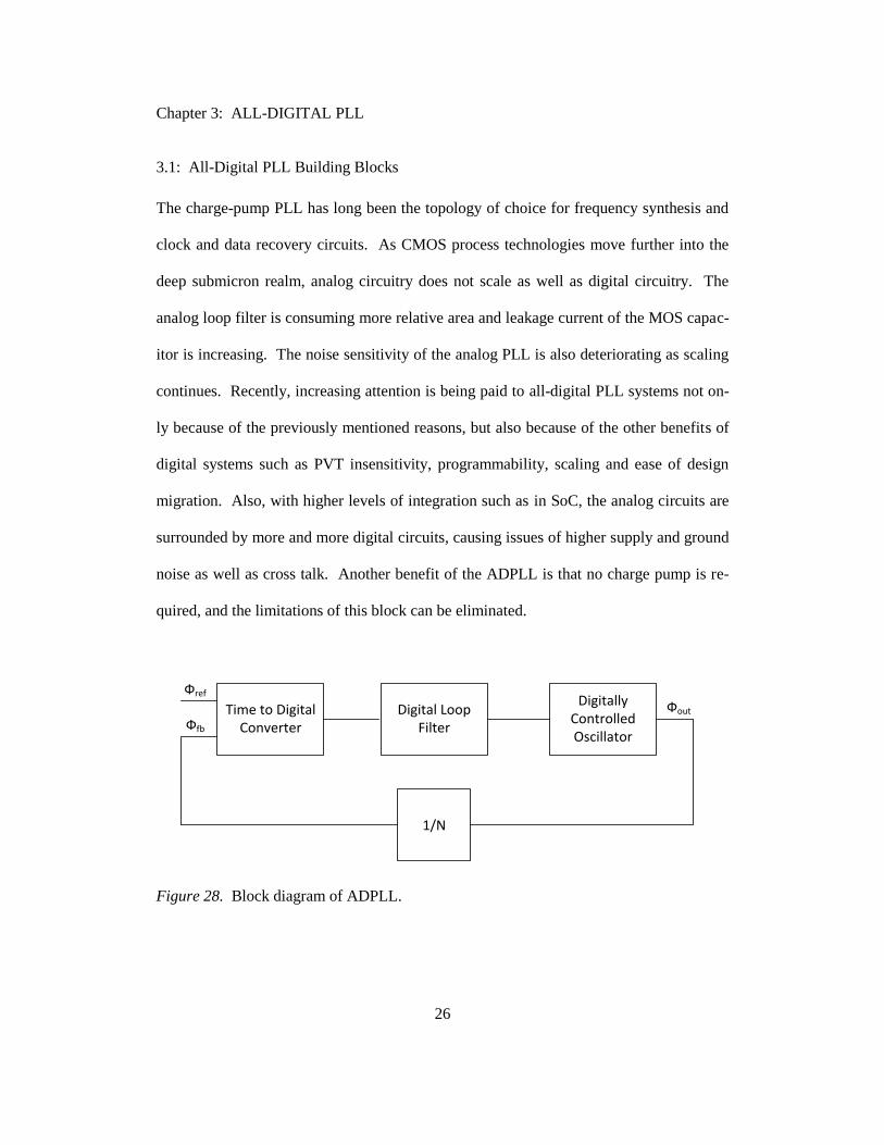
3.1: All-Digital PLL Building Blocks
The charge-pump PLL has long been the topology of choice for frequency synthesis and
clock and data recovery circuits. As CMOS process technologies move further into the
deep submicron realm, analog circuitry does not scale as well as digital circuitry. The
analog loop filter is consuming more relative area and leakage current of the MOS capac-
itor is increasing. The noise sensitivity of the analog PLL is also deteriorating as scaling
continues. Recently, increasing attention is being paid to all-digital PLL systems not on-
ly because of the previously mentioned reasons, but also because of the other benefits of
digital systems such as PVT insensitivity, programmability, scaling and ease of design
migration. Also, with higher levels of integration such as in SoC, the analog circuits are
surrounded by more and more digital circuits, causing issues of higher supply and ground
noise as well as cross talk. Another benefit of the ADPLL is that no charge pump is re-
quired, and the limitations of this block can be eliminated.
Time to Digital Converter
Digital Loop Filter
Digitally Controlled Oscillator
Фref
Фfb
Фout
1/N
Figure 28. Block diagram of ADPLL.
27
3.1.1: Time to Digital Converter
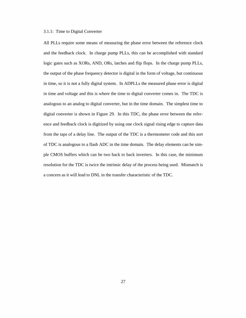
All PLLs require some means of measuring the phase error between the reference clock
and the feedback clock. In charge pump PLLs, this can be accomplished with standard
logic gates such as XORs, AND, ORs, latches and flip flops. In the charge pump PLLs,
the output of the phase frequency detector is digital in the form of voltage, but continuous
in time, so it is not a fully digital system. In ADPLLs the measured phase error is digital
in time and voltage and this is where the time to digital converter comes in. The TDC is
analogous to an analog to digital converter, but in the time domain. The simplest time to
digital converter is shown in Figure 29. In this TDC, the phase error between the refer-
ence and feedback clock is digitized by using one clock signal rising edge to capture data
from the taps of a delay line. The output of the TDC is a thermometer code and this sort
of TDC is analogous to a flash ADC in the time domain. The delay elements can be sim-
ple CMOS buffers which can be two back to back inverters. In this case, the minimum
resolution for the TDC is twice the intrinsic delay of the process being used. Mismatch is
a concern as it will lead to DNL in the transfer characteristic of the TDC.
28
D Q D Q D Q D Q
Фref
Фfb
EncoderT1 T2 T3 T2N
Dout
N
τ τ τ τ
Figure 29. Simple time to digital converter.
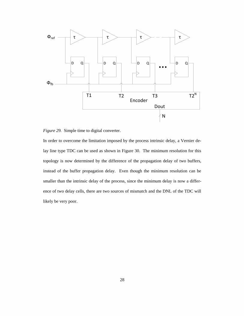
In order to overcome the limitation imposed by the process intrinsic delay, a Vernier de-
lay line type TDC can be used as shown in Figure 30. The minimum resolution for this
topology is now determined by the difference of the propagation delay of two buffers,
instead of the buffer propagation delay. Even though the minimum resolution can be
smaller than the intrinsic delay of the process, since the minimum delay is now a differ-
ence of two delay cells, there are two sources of mismatch and the DNL of the TDC will
likely be very poor.
29
D Q D Q D Q D Q
Фfb
Фref
EncoderT1 T2 T3 T2N
Dout
N
τ1
τ2
τ1
τ2
τ1
τ2
τ1
τ2
Figure 30. Vernier delay line based TDC.
The two TDC topologies discussed so far will have a limited linear range if the total de-
lay from the first buffer to the last is less than the unit interval. This means that the range
of phase error is limited by the number of buffer stages and the delay of each stage.
Mismatch and PVT variations will change the linear range as well as the gain of the TDC
due to variations in each buffer propagation delay. A delay locked loop (DLL) can be
used to ensure the total delay through the chain of buffers is exactly equal to the unit in-
terval, thus giving maximum linear range and gain accuracy to the TDC. This is shown
in Figure 31. While this method improves the performance of the delay line based TDC,
it not only adds complexity, but also an analog block, the DLL, which is not favorable in
ADPLLs.
30
D Q D Q D Q D Q
Фfb
Фref
EncoderT1 T2 T3 T2N
Dout
N
Ф1
Ф2Vc
PD + Loop Filter
τ ττ τ
Figure 31. TDC using DLL to control the delay.
∆Ф
Dout
Figure 32. Generic transfer function of TDC.
31
Another type of TDC utilizes the random nature of input threshold offset of latches and
finite slope of the clock signals to determine the phase error. The stochastic TDC, shown
in Figure 33, is composed of many latches whose input offset varies stochastically due to
process variations. Since the input to each latch has a finite slope these different input
offsets translate into thresholds in time which the reference and the feedback clock sig-
nals are connected to the inputs. If enough of these latches are used, the threshold offsets
and thus time offsets will follow a normal or Gaussian distribution. The outputs of the
latches are summed with the encoder and this output will essentially be the integration of
a Gaussian random variable and the transfer function is approximately linear in the
locked condition where the phase difference is small. The linearized gain of the STDC in
locked condition is given in Equation 23 [19]:
√
Here, NARBS is the number of latches or arbiters, SL is the slope of the clock signal, and
σv is the standard deviation of the voltage threshold of the latches.
(23)
32
Фref
ФfbD1
D2
D2N
Dout
Encoder
N
Figure 33. Stochastic TDC.
∆Ф
ϵ[n]
+1
-1
Figure 34. Stochastic TDC transfer characteristic.
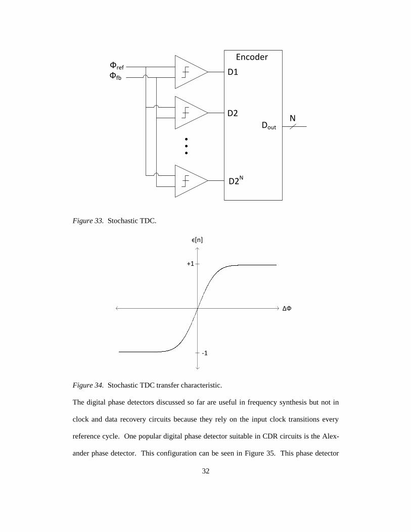
The digital phase detectors discussed so far are useful in frequency synthesis but not in
clock and data recovery circuits because they rely on the input clock transitions every
reference cycle. One popular digital phase detector suitable in CDR circuits is the Alex-
ander phase detector. This configuration can be seen in Figure 35. This phase detector
33
oversamples the random input data by a factor of two and gives an indication of the phase
difference. This architecture can determine if the data is leading or lagging the sampling
clock and can also generate a no change signal when there is no data transition during the
recovered clock period. For this reason, this topology is sometimes called a ternary
phase detector.
Фfb
D Q
D Q
D Q
D Q
DIN Y+
Y-
Figure 35. Alexander phase detector.
The lead-lag or bang-bang phase detector is basically a single bit TDC which outputs a
digital ‘1’ or ‘0’ depending on whether the feedback signal is leading or lagging with re-
spect to the reference signal. The single bit nature of the BBPD makes it very difficult to
analyze the PLL by linearizing the transfer function of the BBPD because the gain is un-
defined. The simplest BBPD can be constructed using a D flip flop as shown in Figure
36. Benefits of such a structure are simplicity and high speed limited only by the speed
of the fastest FF that can be designed in a given process. Another subtle advantage of
using a DFF over an Alexander phase detector is that the multi-phase sampling nature of
the latter leads to a dead zone in the linearized phase detector transfer function as dis-
cussed in [17].
34
D QФref
Фfb
ϵ[n]
∆Ф
ϵ[n]
+1
-1
Figure 36. Bang-bang phase detector and transfer characteristic.
As discussed in [9], [17], [22] and [38], the gain of the BPD can be linearized in the pres-
ence of input reference clock jitter assuming it has a Gaussian distribution and the linear
range is approximately twice the standard deviation of the jitter. The offset of the FF
translates to a static phase offset in the ADPLL, so it can be neglected in the small signal
AC analysis. The transfer function is very similar to the stochastic TDC, since the gain is
derived based on statistical analysis. This method of linearizing binary TDC will be cov-
ered in more detail in section 4.4.2.
The charge pump PLL utilizes a phase frequency detector which simultaneously provides
an indication of phase and frequency error. Some research has focused on digital PFDs.
[46] implements the digital PFD shown in Figure 37. This implementation generates a
single bit which indicates the polarity of the phase error shown here as PE, and another
signal, FAST, which indicates a magnitude of phase error greater than π. A frequency
decision circuit is used to increase or decrease frequency based on whether there are only
UPs or DNs in a decision period. [21] implements a similar circuit using with a multibit
TDC in Simulink to model the behavior of the digital PFD.
35
Фref
Фfb
TDC PE
D Q
rst
D Q
rst
D Q
D Q
Фref
Фfb
UP
DN FAST
Figure 37. Digital PFD.
[44] uses another configuration where the UP and DN signals of the PFD are used in the
proportional path and this is added to an integral path with consists of an accumulated
output of a DFF which is sampled on the rising edge of the DN signal from the same
PFD. [39] implements a digital bang-bang PFD which provides an indication of which
clock signal is faster during frequency acquisition and once the frequencies of the two
clock signals are close, the circuit indicates which signal is leading or lagging.
3.1.2: Digital Loop Filter
The digital output from the TDC must be averaged to provide the control word to the dig-
itally controlled oscillator. For the typical analog PLL with 2nd
order loop filter, the
backward Euler s-to-z transformation can be performed to determine the digital imple-
mentation of this filter. Shown in Figure 38 is the typical s-domain of the analog loop
filter that follows the charge pump of a CPPLL and the digital equivalent. The digital
loop filter is a has proportional and integral branches each with gain of Kp and Ki respec-
tively.
36
C2
C1
R1
ICP(t)
+
-
Vctrl(t)
R1
1/C1
ICP(s) Vctrl(s)
S-1
∑ +
+
Z-1
KP
KI
ϵ(z) Dfine(z)
∑
∑
+
+
+
+
Figure 38. Continuous and discrete time equivalent loop filters.
3.1.3: Digitally Controlled Oscillator
The digitally controlled oscillator is the digital counterpart to the VCO in charge pump
PLLs. The output frequency of a DCO is controlled by a digital word instead of an ana-
log control voltage or current. In an analog PLL, noise on the control voltage line propa-
gates to the output in the form of jitter. Digital control improves the noise immunity of
this very critical component of the PLL.
There are several methods to implement digital control of the output frequency. Direct
digital synthesis is one method of generating an output frequency which is proportional to
the decimal value of a control word. The output frequency can be generated by using a
look up table. Various waveforms such as triangle waves, sine waves or square waves
can be generated at various frequencies based on the reference clock frequency and the
tuning word. Direct digital synthesizers, however, require a reference clock of at least
twice the synthesized frequency, which is of little use in clock multiplier applications.
37
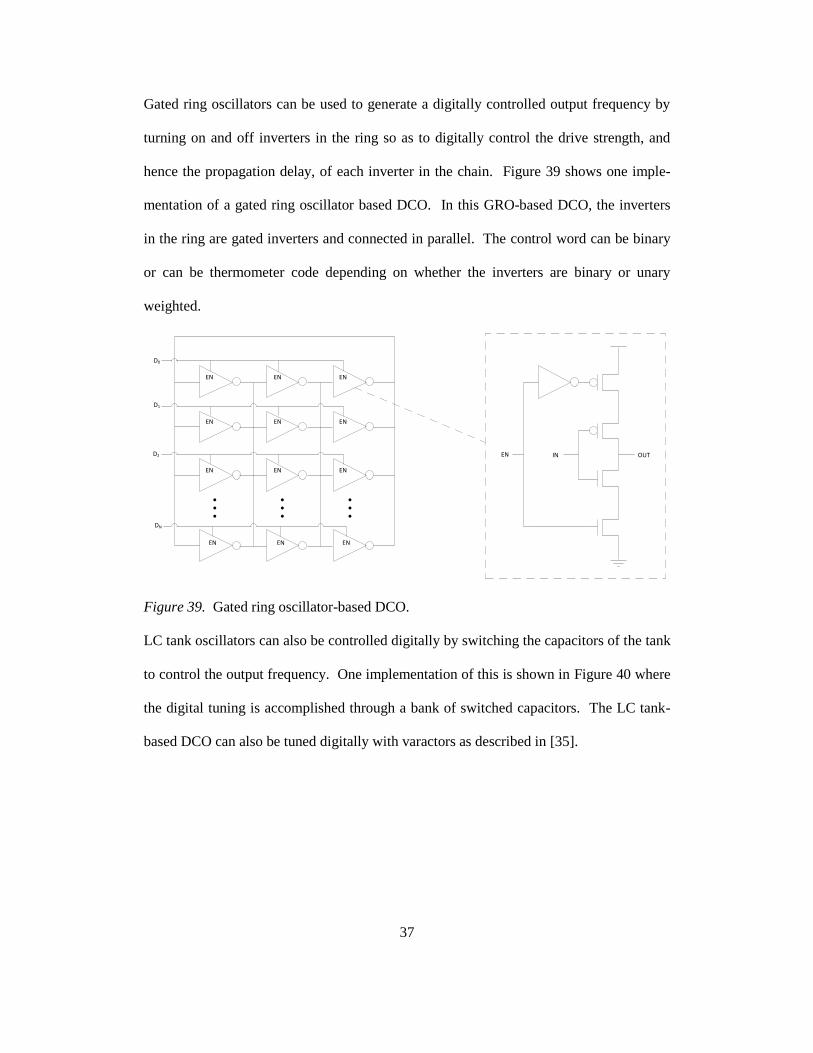
Gated ring oscillators can be used to generate a digitally controlled output frequency by
turning on and off inverters in the ring so as to digitally control the drive strength, and
hence the propagation delay, of each inverter in the chain. Figure 39 shows one imple-
mentation of a gated ring oscillator based DCO. In this GRO-based DCO, the inverters
in the ring are gated inverters and connected in parallel. The control word can be binary
or can be thermometer code depending on whether the inverters are binary or unary
weighted.
EN IN OUT
EN EN EN
EN EN EN
EN EN EN
EN EN EN
D0
D1
D2
DN
Figure 39. Gated ring oscillator-based DCO.
LC tank oscillators can also be controlled digitally by switching the capacitors of the tank
to control the output frequency. One implementation of this is shown in Figure 40 where
the digital tuning is accomplished through a bank of switched capacitors. The LC tank-
based DCO can also be tuned digitally with varactors as described in [35].
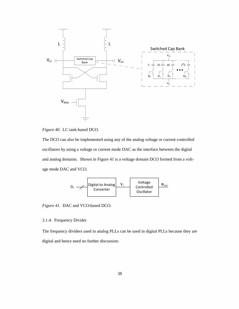
38
Vo+Vo-
Vbias
Switched Cap Bank
D0 D1 D2
C 2C 4C
DN
2NC
Vo-
Vo+
Switched Cap BankL L
Figure 40. LC tank-based DCO.
The DCO can also be implemented using any of the analog voltage or current controlled
oscillators by using a voltage or current mode DAC as the interface between the digital
and analog domains. Shown in Figure 41 is a voltage domain DCO formed from a volt-
age mode DAC and VCO.
Voltage Controlled Oscillator
ФoutDigital to Analog Converter
DcVc
Figure 41. DAC and VCO-based DCO.
3.1.4: Frequency Divider
The frequency dividers used in analog PLLs can be used in digital PLLs because they are
digital and hence need no further discussion.
39
3.2: Limit Cycles and Quantization Noise in ADPLLs
Due to the finite nature of the signals in the ADPLL, there will inevitably be quantization
noise sources due to the phase to digital conversion from the TDC and the digital to fre-
quency conversion from the DCO. The quantization noise can be modeled in a similar
fashion to data conversion systems where the TDC and DCO are analogous to an ADC
and DAC, respectively. In ADPLLs with binary phase detectors, a limit cycle occurs due
to the non-linearity introduced into the loop. These effects will be considered further in
section 4.4.2.
3.3: State of the Art
An MDLL based digitally intensive clock multiplier is presented in [18]. This design
makes use of a new correlated double sampling method to reduce path delay mismatch
effects which lead to increased deterministic jitter. The DLL tuning voltage is generated
differently than the traditional MDLL based synthesizer. The TDC is GRO based and the
phase error is calculated by sampling the pulse width of the ring oscillator period and the
ring oscillator period plus the additional error due to the replacement of every Nth edge
of the ring oscillator output. This topology first processes the digital error signal and then
converts it to an analog voltage with a DAC and performs additional analog processing
using an RC filter. Total rms jitter was reported to be 930 fs at 1.6 GHz in 0.13 um
CMOS process at an estimated 9.1 mW overall power consumption. The total peak to
peak jitter was reported to be 11.1 ps with 760 fs estimated deterministic jitter. Phase
noise was reported to be -58.3 dBc at 50 MHz offset.
In [39] an all static CMOS ADPLL is designed on 65 nm CMOS SOI process. The
ADPLL utilizes a 3 stage, static inverter based ring oscillator DCO. The design also uti-
lizes a BBPFD which is acceptable due to relaxed noise and bandwidth requirements.
40
The topology does not use an explicit DAC, but instead directly converts from digital to
frequency using the GRO DCO. The design also utilizes a programmable PID controller
and third order MASH sigma-delta for the LSB of the DCO. The sigma-delta modulation
of the LSBs helps to noise shape the phase noise generated by the limit cycle caused by
the BBPD. This work reports 32 mW power consumption and 6 ps rms jitter at 1.2 V
supply and 4 GHz output frequency.
In [35], an ADPLL is fabricated on 90 nm CMOS process as part of a single-chip
GSM/EDGE transceiver. This work utilizes an LC oscillator as the DCO which is pro-
grammable by using varactor banks. A very interesting feature in this paper is the opera-
tion of the ADPLL in a digitally synchronous fixed-point phase domain. This is unlike
traditional charge pump PLLs whose phase detection mechanism is correlational and
causes significant spurs. The output phase is first measured by accumulating clock edg-
es which gives a coarse indication of the output phase. A TDC is used to generate a
phase error signal with finer resolution. The digital derivative of the output phase and the
phase error is taken to provide a frequency signal which is subtracted from a frequency
command word. This frequency error is then accumulated to produce an equivalent
phase error and processed by a digital 4-pole IIR filter. The output of the filter then con-
trols the DCO. This topology reports phase noise of -122 dBc/Hz at 400 kHz offset.
[23] describes the design of an ADPLL for wireless applications in the WiMAX 3.3-3.8
GHz bandwidth in 90 nm CMOS process. This design utilizes a DLL based TDC to de-
crease sensitivity to PVT variations and also uses a BBPD and digital loop filter. Spurs
generated by skew between a counter and TDC are corrected by glitch detection logic.
The DCO is composed of a LC tank based oscillator that is digitally tuned by a switched
capacitor bank in the LC tank. The frequency and phase error are measured similar to
41
[35] and the frequency error signal is digitally integrated and fed to a digital PI filter.
This work reports in band phase noise of -95 dBc/Hz.
[24] describes the design of an ADPLL in 180 nm CMOS technology which achieves 210
ps peak to peak jitter. This ADPLL is based on a two loop architecture for fine and
coarse frequency tuning of a DCO (or RCO as it is referred to in the literature). Coarse
tuning is performed using a digitally controlled symmetrical delay line and fine tuning is
done with capacitor banks. An all-digital PFD is used as well to provide digital phase
and frequency error detection. The ADPLL in this case is used for clock synchronization
for a memory interface at 200 MHz and consumes 5.9 mW at supply of 2.5 V.
In [46], a 4 GHz ADPLL is fabricated on 90 nm CMOS technology for frequency synthe-
sis which features programmable loop bandwidth from 100 kHz to 6 MHz. The DCO in
this work is the LC-tank based oscillator with capacitor bank for frequency tuning. The
work uses a digital PFD composed of a conventional tri-state PFD and BBPD. The con-
trol loop uses a digital PI controller as the loop filter. This work reports phase noise at 1
MHz offset as -106 dBc/Hz.
[20] describes the design of an ADPLL using a 6-bit stochastic TDC for phase control
and BBPFD for frequency control. This design also uses delta-sigma dithering to im-
prove bandwidth and minimize jitter. The DCO is composed of a current steering DAC,
current to voltage converter and a differential ring oscillator VCO. This design was fab-
ricated on 130 nm CMOS technology and reports 6.9 ps rms jitter and 56 ps peak to peak
jitter with a tuning range of 0.7 to 1.7 GHz tuning range at 17 mW (at 1.2 GHz) from a
1.2 V supply.
In [3] a DLL based frequency multiplier is implemented in 0.35 µm CMOS technology
for use as a 900 MHz frequency synthesizer for a wireless application. In this design, the
spectrally pure crystal oscillator clock signal is fed into a DLL to produce evenly spaced
42
clock edges and these clock edges are combined with digital logic to produce a low jitter
output clock. This output frequency is a multiple of the reference frequency determined
by the number of delay stages in the DLL. The DLL in this design still relies on tradi-
tional analog functions of phase detection, charge pump and loop filtering. This design
achieves -123 dBc/Hz at 60 kHz offset and consumes 130 mW from a 3.3 V supply. A
similar approach is used in [2] for a 108 MHz synthesized clock for an 8-bit video-rate
DAC and reports 80 ps jitter and 0.9 mW from 3.3 V supply on 0.5 µm CMOS process.
In [42], an ADPLL frequency synthesizer with dynamically reconfigurable digital loop
filter coefficients is designed on 90 nm CMOS process. The digital loop filter coeffi-
cients are adjusted by a locking process monitor circuit which improves lock time with-
out sacrificing jitter performance. The design is a dual loop design with frequency and
phase lock loops. This design uses a DCO composed of an LC oscillator with digitally
tunable varactor banks. The work reports 7.1 mW from 1 V power supply with 0.9 ps
rms jitter at 10 GHz.
43
Chapter 4: CIRCUIT DESIGN AND IMPLEMENTATION
4.1: Application
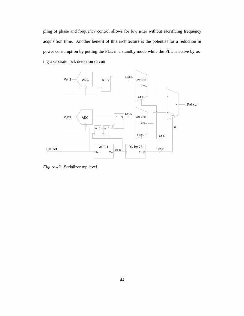
The DPLL is designed to be used in a read out integrated circuit (ROIC) which is con-
nected to a focal plane array (FPA) in order to digitize and serialize the incoming image
data, essentially serving as the analog front end (AFE) of the imaging system. The sys-
tem needs to be operational at room temperature and optimized for operation at -195 °C.
The digitized data is sent outside of the ROIC to an FPGA for further processing. The
ADPLL will generate the 280 MHz clock signal used in the serializer circuit. The serial-
izer in this application will interface two parallel 14 bit ADC outputs and combine them
into a serial output at a frequency 28 times the sampling frequency. The ADC sampling
frequency for this application is a stable 10 MHz generated from a crystal oscillator,
which necessitates an output frequency of 280 MHz. This system is shown in Figure 42
and 43. Not shown is the circuitry used to synchronize the counter in the divider with the
rising edge of the reference clock.
An all-digital PLL was chosen instead of the traditional analog PLL because of the pro-
grammability, lower power, higher noise immunity and portability of digital systems.
Since the system will be operating at cryogenic temperatures around -195 °C, power con-
sumption is a critical performance parameter because for every 1 mW consumed in a cry-
ogenic dewar, 40 mW is used to remove the heat. The system must be immune to single
event effects (SEEs) and latch up. The process chosen for integration is Jazz’s CA18HD
process.
The two loop PLL and FLL architecture was chosen as opposed to summing the frequen-
cy and phase errors together and passing them through a single loop filter or using a digi-
tal PFD. The primary motive for using two separate control loops is flexibility. Decou-
44
pling of phase and frequency control allows for low jitter without sacrificing frequency
acquisition time. Another benefit of this architecture is the potential for a reduction in
power consumption by putting the FLL in a standby mode while the PLL is active by us-
ing a separate lock detection circuit.
Dataout
S<3:0>
Data<13:0>
Dataout
S<3:0>
Data<13:0>
Dataout
S0
A
Y
B
ADPLL Div by 28Clk_ref
ΦREF Φout
Clk_28S<4:0>
S4
S<3:0>
A<13:0>
S<4:0>
ADC
ADC
VA(t)
VB(t)B<13:0>
D Q
D Q
D Q D Q
Figure 42. Serializer top level.
45
A
B
S0
A
B
S0S1
C
D
Y
A
B
S0S1
C
D
Y
A
B
S0S1
C
D
Y
A
B
S0S1
C
D
Y
S2S3
Data<0>
Data<1>
Data<2>
Data<3>
Data<4>
Data<5>
Data<6>
Data<7>
Data<8>
Data<9>
Data<10>
Data<11>
Data<12>
Data<13>Y
Dataout
S0S1
S0S1
S0S1
S0
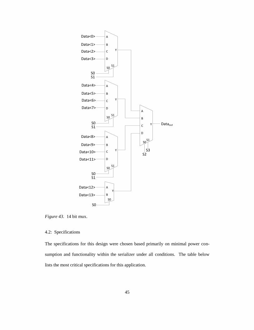
Figure 43. 14 bit mux.
4.2: Specifications
The specifications for this design were chosen based primarily on minimal power con-
sumption and functionality within the serializer under all conditions. The table below
lists the most critical specifications for this application.
46
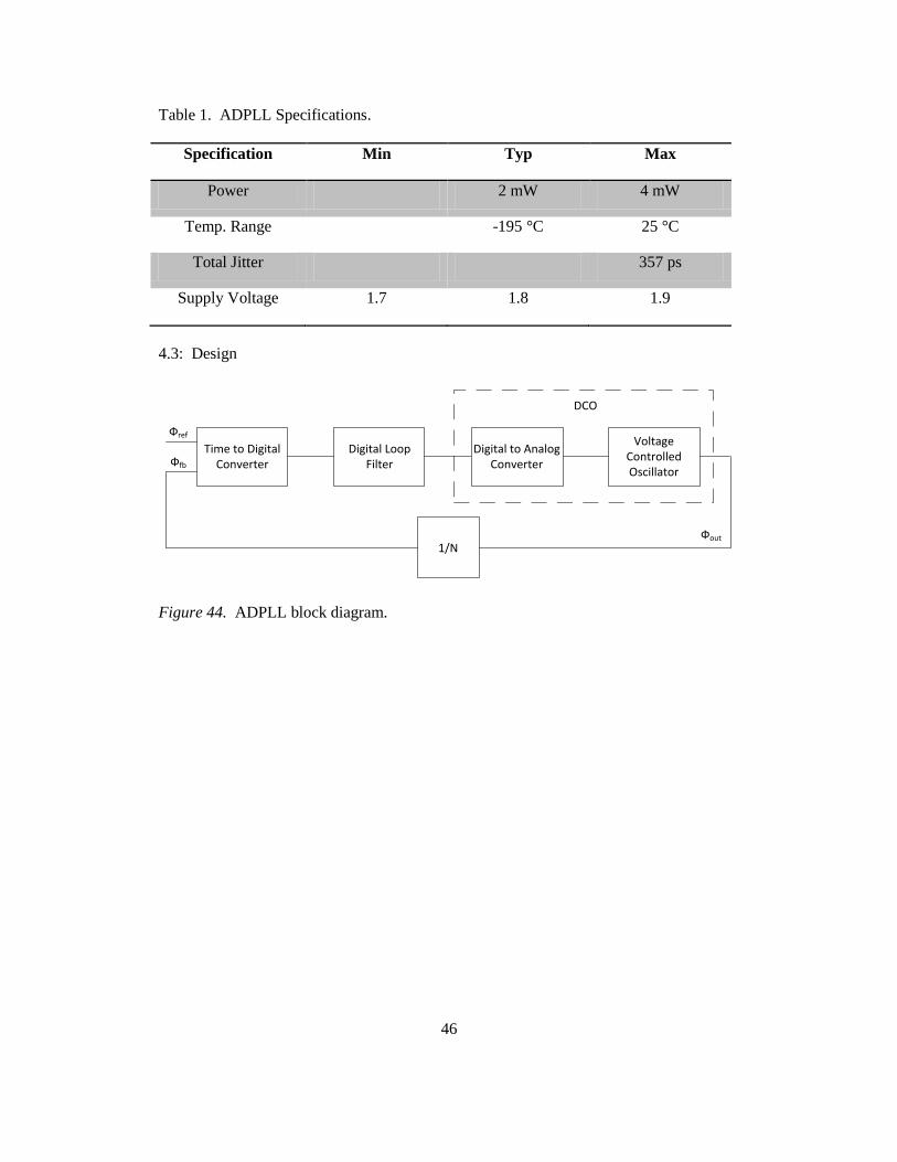
Table 1. ADPLL Specifications.
Specification Min Typ Max
Power 2 mW 4 mW
Temp. Range -195 °C 25 °C
Total Jitter 357 ps
Supply Voltage 1.7 1.8 1.9
4.3: Design
Time to Digital Converter
Digital Loop Filter
Voltage Controlled Oscillator
Фref
Фfb
Фout
Digital to Analog Converter
DCO
1/N
Figure 44. ADPLL block diagram.
47
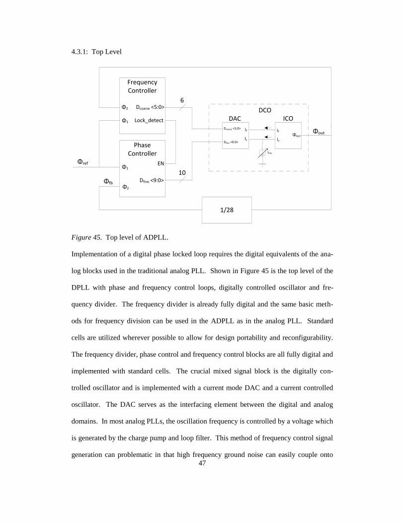
4.3.1: Top Level
Frequency Controller
Phase Controller
DCO
1/28
ICODAC
Φref
Φout
Φfb
6
10
Dcoarse <5:0>
Dfine <9:0>
If
Ic
Φout
Φ1
Φ2
Φ1
Φ2 Dcoarse <5:0>
Dfine <9:0>
EN
Lock_detect
Ic
If
ICAL
Figure 45. Top level of ADPLL.
Implementation of a digital phase locked loop requires the digital equivalents of the ana-
log blocks used in the traditional analog PLL. Shown in Figure 45 is the top level of the
DPLL with phase and frequency control loops, digitally controlled oscillator and fre-
quency divider. The frequency divider is already fully digital and the same basic meth-
ods for frequency division can be used in the ADPLL as in the analog PLL. Standard
cells are utilized wherever possible to allow for design portability and reconfigurability.
The frequency divider, phase control and frequency control blocks are all fully digital and
implemented with standard cells. The crucial mixed signal block is the digitally con-
trolled oscillator and is implemented with a current mode DAC and a current controlled
oscillator. The DAC serves as the interfacing element between the digital and analog
domains. In most analog PLLs, the oscillation frequency is controlled by a voltage which
is generated by the charge pump and loop filter. This method of frequency control signal
generation can problematic in that high frequency ground noise can easily couple onto
48
this node and cause jitter on the output of the oscillator. Another disadvantage of voltage
signal control of frequency is that the large filter capacitors that are typically implement-
ed with MOS capacitors with large leakage currents. The following sections will discuss
the individual blocks in detail.
4.3.2: Frequency Divider
The frequency divider is similar to the frequency dividers previously discussed. The out-
put of the oscillator is used in a binary up counter and reset to zero when it hits the deci-
mal equivalent of 13, which is a total of 14 counts. The falling edge of the MSB of the
count clocks a basic divide-by-two circuit for an output frequency of
. This output
frequency is fed back to the BBPD for phase detection.
J
K
Q
Q J
K
Q
Q J
K
Q
Q J
K
Q
Q
Φout
J
K
Q0
Q1N
Q2
Q3
J
K
Q0
Q1N
Q2
Q3
J
K
Q0
Q1N
Q2
Q3
D D D
D
Q
Q
Q1N
Q1
Q0
Q2
Q3Q0
Q2
Q3
Q0
Q3
Q1N
Q2
Q3
Q1N
Reset Logic Reset Logic Reset Logic
Φfb
Figure 46. Frequency divider.
J
K
Q0
Q1N
Q2Q3
D A
B
S0
Y
A
B
S0
Y
Figure 47. Reset logic.
49
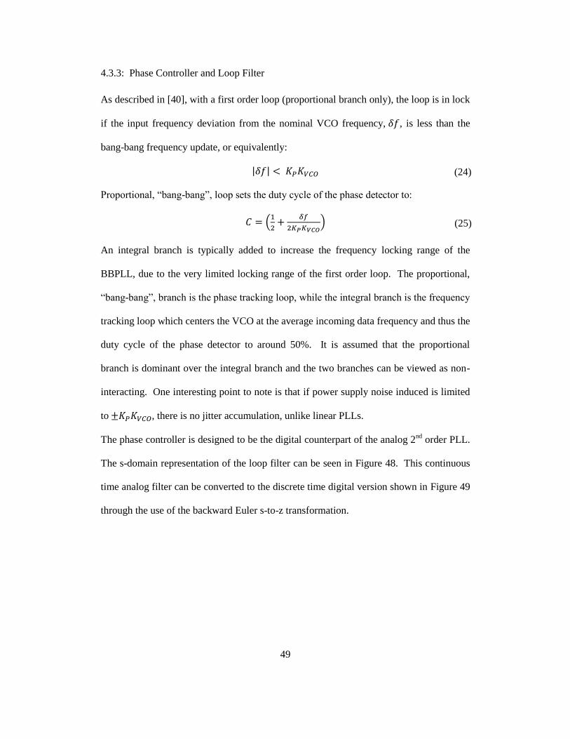
4.3.3: Phase Controller and Loop Filter
As described in [40], with a first order loop (proportional branch only), the loop is in lock
if the input frequency deviation from the nominal VCO frequency, , is less than the
bang-bang frequency update, or equivalently:
| |
Proportional, “bang-bang”, loop sets the duty cycle of the phase detector to:
(
)
An integral branch is typically added to increase the frequency locking range of the
BBPLL, due to the very limited locking range of the first order loop. The proportional,
“bang-bang”, branch is the phase tracking loop, while the integral branch is the frequency
tracking loop which centers the VCO at the average incoming data frequency and thus the
duty cycle of the phase detector to around 50%. It is assumed that the proportional
branch is dominant over the integral branch and the two branches can be viewed as non-
interacting. One interesting point to note is that if power supply noise induced is limited
to , there is no jitter accumulation, unlike linear PLLs.
The phase controller is designed to be the digital counterpart of the analog 2nd
order PLL.
The s-domain representation of the loop filter can be seen in Figure 48. This continuous
time analog filter can be converted to the discrete time digital version shown in Figure 49
through the use of the backward Euler s-to-z transformation.
(24)
(25)
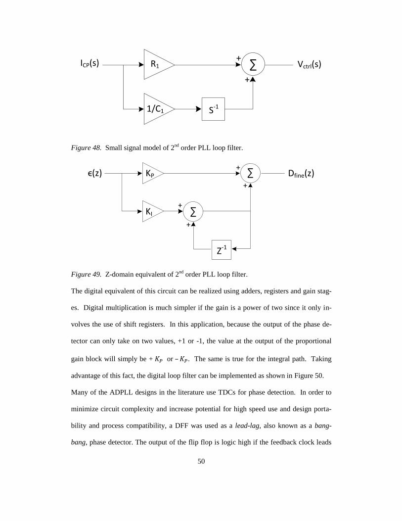
50
R1
1/C1
ICP(s) Vctrl(s)
S-1
∑ +
+
Figure 48. Small signal model of 2nd
order PLL loop filter.
Z-1
KP
KI
ϵ(z) Dfine(z)
∑
∑
+
+
+
+
Figure 49. Z-domain equivalent of 2nd
order PLL loop filter.
The digital equivalent of this circuit can be realized using adders, registers and gain stag-
es. Digital multiplication is much simpler if the gain is a power of two since it only in-
volves the use of shift registers. In this application, because the output of the phase de-
tector can only take on two values, +1 or -1, the value at the output of the proportional
gain block will simply be + or – . The same is true for the integral path. Taking
advantage of this fact, the digital loop filter can be implemented as shown in Figure 50.
Many of the ADPLL designs in the literature use TDCs for phase detection. In order to
minimize circuit complexity and increase potential for high speed use and design porta-
bility and process compatibility, a DFF was used as a lead-lag, also known as a bang-
bang, phase detector. The output of the flip flop is logic high if the feedback clock leads
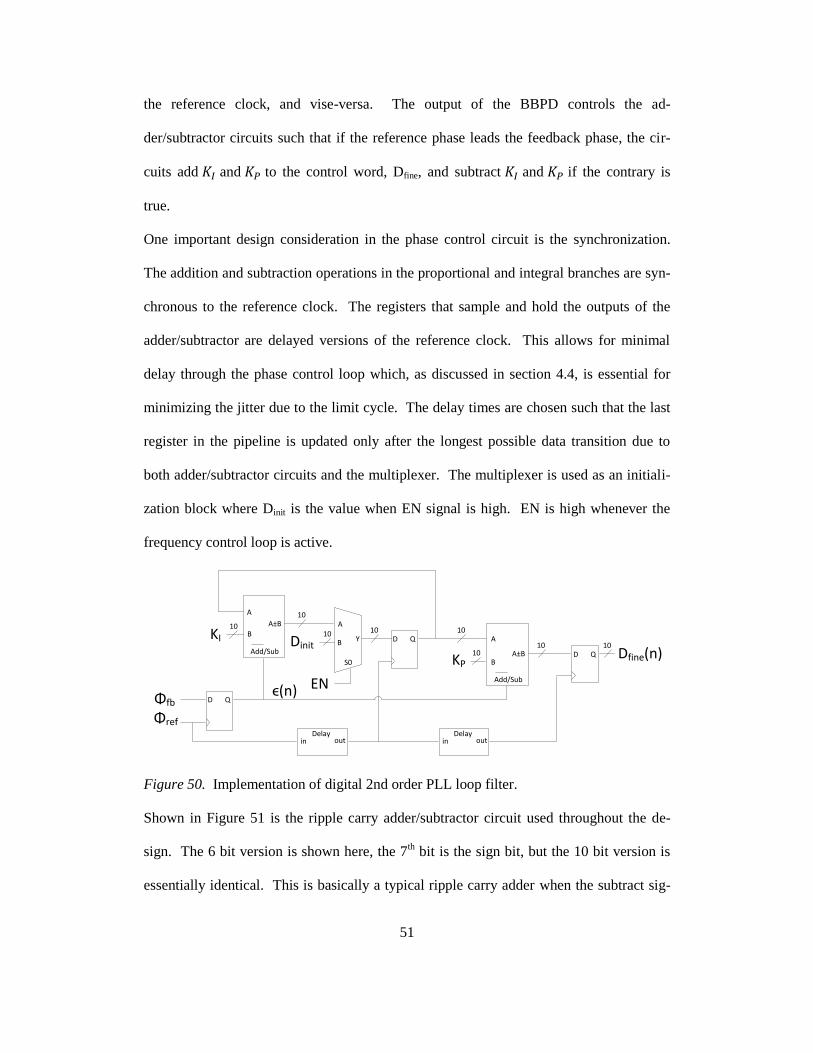
51
the reference clock, and vise-versa. The output of the BBPD controls the ad-
der/subtractor circuits such that if the reference phase leads the feedback phase, the cir-
cuits add and to the control word, Dfine, and subtract and if the contrary is
true.
One important design consideration in the phase control circuit is the synchronization.
The addition and subtraction operations in the proportional and integral branches are syn-
chronous to the reference clock. The registers that sample and hold the outputs of the
adder/subtractor are delayed versions of the reference clock. This allows for minimal
delay through the phase control loop which, as discussed in section 4.4, is essential for
minimizing the jitter due to the limit cycle. The delay times are chosen such that the last
register in the pipeline is updated only after the longest possible data transition due to
both adder/subtractor circuits and the multiplexer. The multiplexer is used as an initiali-
zation block where Dinit is the value when EN signal is high. EN is high whenever the
frequency control loop is active.
KP
KI
ϵ(n)
Dfine(n) A
B
Add/Sub
A±B
A
B
Add/Sub
A±B
D Q
A
B
S0
Y
D Q
Dinit
10
1010 10
1010 10
END Q
Φref
Φfb
Delayin out
Delayin out
10
Figure 50. Implementation of digital 2nd order PLL loop filter.
Shown in Figure 51 is the ripple carry adder/subtractor circuit used throughout the de-
sign. The 6 bit version is shown here, the 7th bit is the sign bit, but the 10 bit version is
essentially identical. This is basically a typical ripple carry adder when the subtract sig-
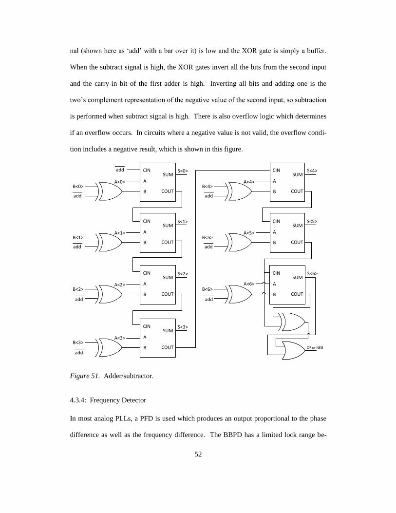
52
nal (shown here as ‘add’ with a bar over it) is low and the XOR gate is simply a buffer.
When the subtract signal is high, the XOR gates invert all the bits from the second input
and the carry-in bit of the first adder is high. Inverting all bits and adding one is the
two’s complement representation of the negative value of the second input, so subtraction
is performed when subtract signal is high. There is also overflow logic which determines
if an overflow occurs. In circuits where a negative value is not valid, the overflow condi-
tion includes a negative result, which is shown in this figure.
CIN
COUT
SUMA
B
CIN
COUT
SUMA
B
CIN
COUT
SUMA
B
CIN
COUT
SUMA
B
CIN
COUT
SUMA
B
CIN
COUT
SUMA
B
S<0>
S<1>
S<2>
S<4>
S<5>
S<6>
add
add
add
add
add
add
add
B<0>A<0>
B<1>A<1>
B<2>A<2>
B<4>A<4>
B<5>A<5>
B<6>A<6>
OF or NEG
CIN
COUT
SUMA
B
S<3>
add
B<3>A<3>
Figure 51. Adder/subtractor.
4.3.4: Frequency Detector
In most analog PLLs, a PFD is used which produces an output proportional to the phase
difference as well as the frequency difference. The BBPD has a limited lock range be-
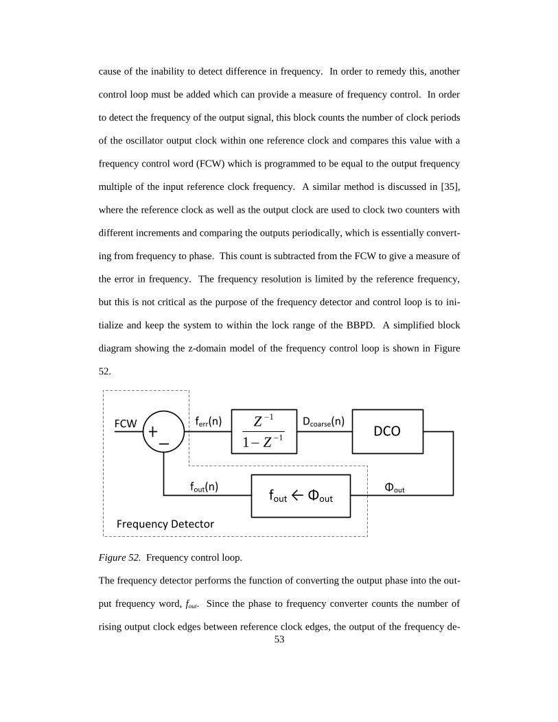
53
cause of the inability to detect difference in frequency. In order to remedy this, another
control loop must be added which can provide a measure of frequency control. In order
to detect the frequency of the output signal, this block counts the number of clock periods
of the oscillator output clock within one reference clock and compares this value with a
frequency control word (FCW) which is programmed to be equal to the output frequency
multiple of the input reference clock frequency. A similar method is discussed in [35],
where the reference clock as well as the output clock are used to clock two counters with
different increments and comparing the outputs periodically, which is essentially convert-
ing from frequency to phase. This count is subtracted from the FCW to give a measure of
the error in frequency. The frequency resolution is limited by the reference frequency,
but this is not critical as the purpose of the frequency detector and control loop is to ini-
tialize and keep the system to within the lock range of the BBPD. A simplified block
diagram showing the z-domain model of the frequency control loop is shown in Figure
52.
Φoutfout ← Φout
ferr(n)
1
1
1
Z
Z
fout(n)
DCODcoarse(n)FCW
Frequency Detector
Figure 52. Frequency control loop.
The frequency detector performs the function of converting the output phase into the out-
put frequency word, fout. Since the phase to frequency converter counts the number of
rising output clock edges between reference clock edges, the output of the frequency de-
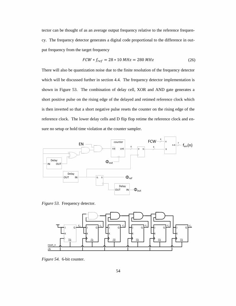
54
tector can be thought of as an average output frequency relative to the reference frequen-
cy. The frequency detector generates a digital code proportional to the difference in out-
put frequency from the target frequency
There will also be quantization noise due to the finite resolution of the frequency detector
which will be discussed further in section 4.4. The frequency detector implementation is
shown in Figure 53. The combination of delay cell, XOR and AND gate generates a
short positive pulse on the rising edge of the delayed and retimed reference clock which
is then inverted so that a short negative pulse resets the counter on the rising edge of the
reference clock. The lower delay cells and D flip flop retime the reference clock and en-
sure no setup or hold time violation at the counter sampler.
ferr(n) A
B
A-B
D Q
Φref
6
6
counter
rst cnt6
FCW 7
Delay
INOUT
ΦoutDelay
IN OUT
EN
DQ
Delay
INOUT Φout
Figure 53. Frequency detector.
J
K
Q
rst
J
K
Q
rst
J
K
Q
rst
J
K
Q
rst
J
K
Q
rst
J
K
Q
rst
reset_n
clk
C0 C1 C2 C3 C4 C5
Figure 54. 6-bit counter.
(26)
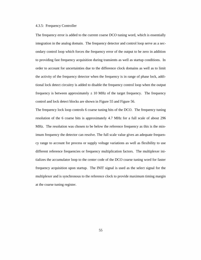
55
4.3.5: Frequency Controller
The frequency error is added to the current coarse DCO tuning word, which is essentially
integration in the analog domain. The frequency detector and control loop serve as a sec-
ondary control loop which forces the frequency error of the output to be zero in addition
to providing fast frequency acquisition during transients as well as startup conditions. In
order to account for uncertainties due to the difference clock domains as well as to limit
the activity of the frequency detector when the frequency is in range of phase lock, addi-
tional lock detect circuitry is added to disable the frequency control loop when the output
frequency is between approximately ± 10 MHz of the target frequency. The frequency
control and lock detect blocks are shown in Figure 55 and Figure 56.
The frequency lock loop controls 6 coarse tuning bits of the DCO. The frequency tuning
resolution of the 6 coarse bits is approximately 4.7 MHz for a full scale of about 296
MHz. The resolution was chosen to be below the reference frequency as this is the min-
imum frequency the detector can resolve. The full scale value gives an adequate frequen-
cy range to account for process or supply voltage variations as well as flexibility to use
different reference frequencies or frequency multiplication factors. The multiplexer ini-
tializes the accumulator loop to the center code of the DCO coarse tuning word for faster
frequency acquisition upon startup. The INIT signal is used as the select signal for the
multiplexer and is synchronous to the reference clock to provide maximum timing margin
at the coarse tuning register.
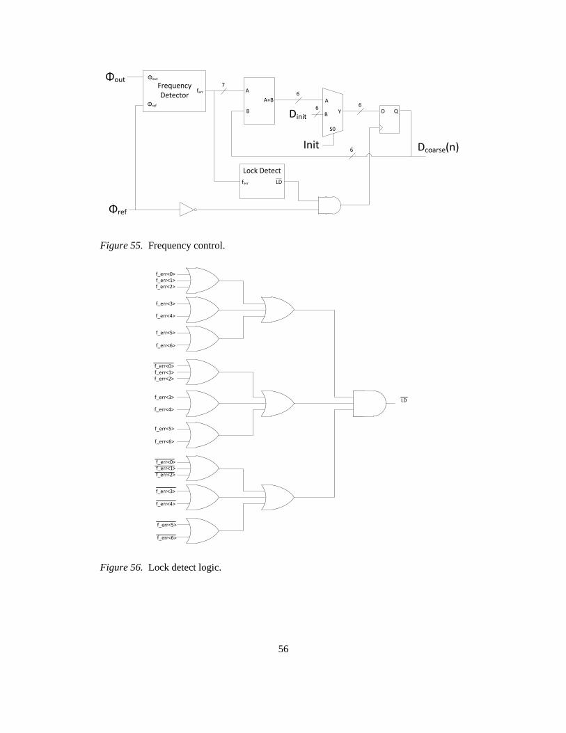
56
Dcoarse(n)
A
B
A+B A
B
S0
Y D QDinit
Φref
6
6 6
6Init
Lock Detect
Frequency Detector
Φout
Φref
ferr
7Φout
LDferr
Figure 55. Frequency control.
f_err<0>f_err<1>
LD
f_err<2>
f_err<3>
f_err<4>
f_err<5>
f_err<6>
f_err<0>f_err<1>f_err<2>
f_err<3>
f_err<4>
f_err<5>
f_err<6>
f_err<0>f_err<1>f_err<2>
f_err<3>
f_err<4>
f_err<5>
f_err<6>
Figure 56. Lock detect logic.
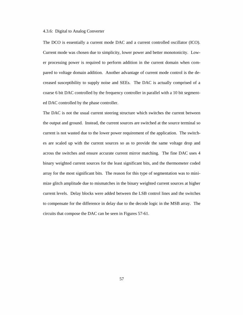
57
4.3.6: Digital to Analog Converter
The DCO is essentially a current mode DAC and a current controlled oscillator (ICO).
Current mode was chosen due to simplicity, lower power and better monotonicity. Low-
er processing power is required to perform addition in the current domain when com-
pared to voltage domain addition. Another advantage of current mode control is the de-
creased susceptibility to supply noise and SEEs. The DAC is actually comprised of a
coarse 6 bit DAC controlled by the frequency controller in parallel with a 10 bit segment-
ed DAC controlled by the phase controller.
The DAC is not the usual current steering structure which switches the current between
the output and ground. Instead, the current sources are switched at the source terminal so
current is not wasted due to the lower power requirement of the application. The switch-
es are scaled up with the current sources so as to provide the same voltage drop and
across the switches and ensure accurate current mirror matching. The fine DAC uses 4
binary weighted current sources for the least significant bits, and the thermometer coded
array for the most significant bits. The reason for this type of segmentation was to mini-
mize glitch amplitude due to mismatches in the binary weighted current sources at higher
current levels. Delay blocks were added between the LSB control lines and the switches
to compensate for the difference in delay due to the decode logic in the MSB array. The
circuits that compose the DAC can be seen in Figures 57-61.
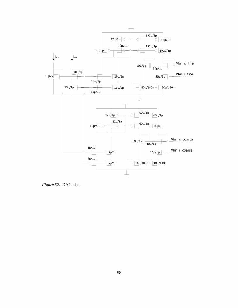
58
Vbn_r_fine
Vbn_c_fine
IB2IB1
Vbn_r_coarse
Vbn_c_coarse
80µ/180n80µ/180n
10µ/5µ
10µ/1µ
10µ/1µ
10µ/1µ
10µ/1µ
10µ/1µ
10µ/1µ
80µ/5µ
80µ/1µ
80µ/1µ
12µ/1µ
12µ/1µ
12µ/5µ
192µ/1µ
192µ/1µ
192µ/1µ
192µ/1µ
5µ/1µ
5µ/1µ
5µ/1µ
5µ/1µ
12µ/1µ
12µ/1µ
12µ/5µ
60µ/1µ60µ/1µ
60µ/1µ60µ/1µ
10µ/180n10µ/180n
10µ/5µ
10µ/1µ
10µ/1µ
Figure 57. DAC bias.
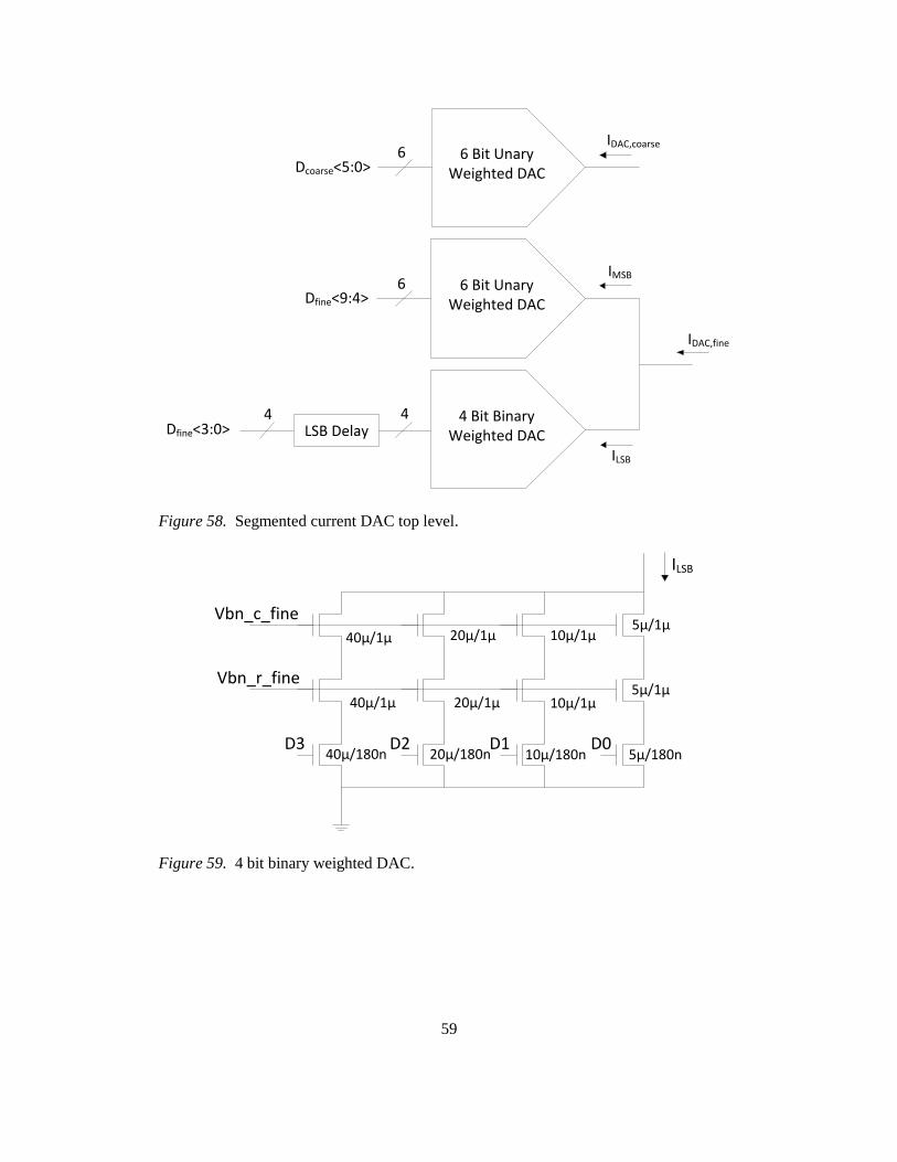
59
6 Bit Unary Weighted DAC
4 Bit Binary Weighted DAC
6
4
Dfine<9:4>
IMSB
ILSB
IDAC,fine
4LSB Delay
6 Bit Unary Weighted DAC
6Dcoarse<5:0>
IDAC,coarse
Dfine<3:0>
Figure 58. Segmented current DAC top level.
Vbn_c_fine
Vbn_r_fine
D3 D2 D1 D0
ILSB
5µ/1µ
5µ/1µ
5µ/180n10µ/180n20µ/180n40µ/180n
10µ/1µ20µ/1µ40µ/1µ
10µ/1µ20µ/1µ40µ/1µ
Figure 59. 4 bit binary weighted DAC.
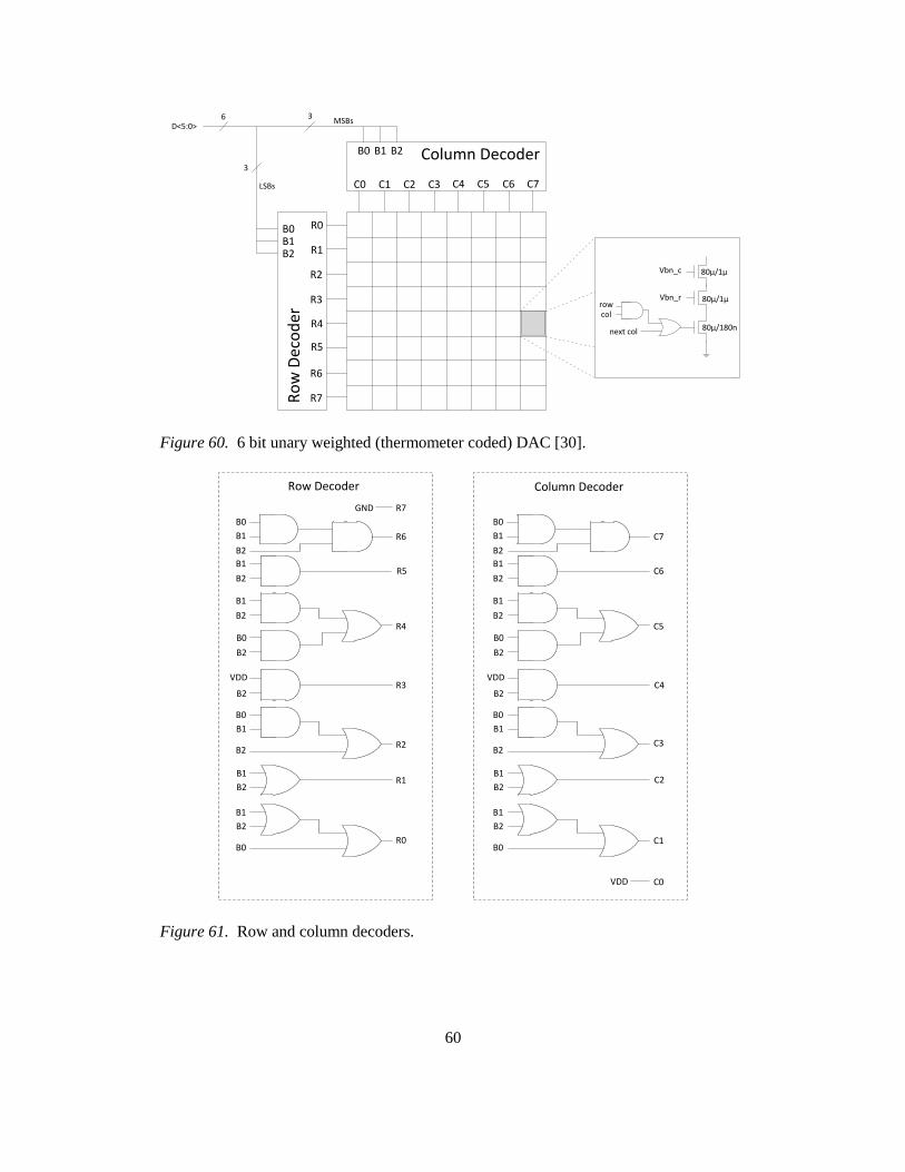
60
Vbn_c
Vbn_rrowcol
next col
Column Decoder
Ro
w D
eco
der
R0
R1
R2
R3
R4
R5
R6
R7
B0B1B2
B0 B1 B2
C0 C1 C2 C3 C4 C5 C6 C7
D<5:0>6
3
3MSBs
LSBs
80µ/1µ
80µ/1µ
80µ/180n
Figure 60. 6 bit unary weighted (thermometer coded) DAC [30].
B0
B1
B2
B1
B2
B1
B2
B0
B2
B2
VDD
B0
B1
B2
B1
B2
B1
B2
B0
B0
B1
B2
B1
B2
B1
B2
B0
B2
B2
VDD
B0
B1
B2
B1
B2
B1
B2
B0
C7
C6
C5
C4
C3
C2
C1
C0VDD
R0
R1
R2
R3
R4
R5
R6
R7GND
Row Decoder Column Decoder
Figure 61. Row and column decoders.
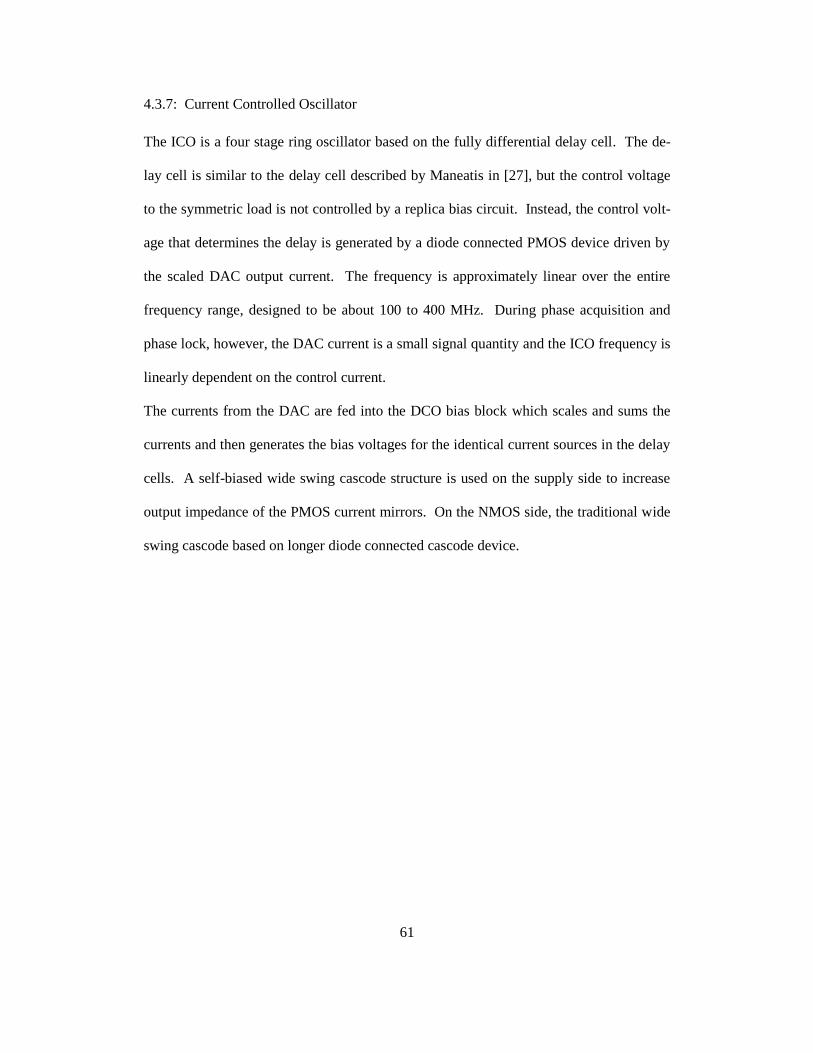
61
4.3.7: Current Controlled Oscillator
The ICO is a four stage ring oscillator based on the fully differential delay cell. The de-
lay cell is similar to the delay cell described by Maneatis in [27], but the control voltage
to the symmetric load is not controlled by a replica bias circuit. Instead, the control volt-
age that determines the delay is generated by a diode connected PMOS device driven by
the scaled DAC output current. The frequency is approximately linear over the entire
frequency range, designed to be about 100 to 400 MHz. During phase acquisition and
phase lock, however, the DAC current is a small signal quantity and the ICO frequency is
linearly dependent on the control current.
The currents from the DAC are fed into the DCO bias block which scales and sums the
currents and then generates the bias voltages for the identical current sources in the delay
cells. A self-biased wide swing cascode structure is used on the supply side to increase
output impedance of the PMOS current mirrors. On the NMOS side, the traditional wide
swing cascode based on longer diode connected cascode device.
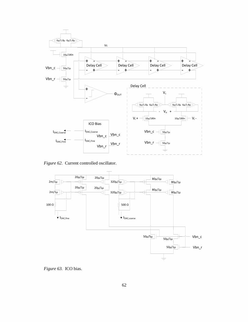
62
Vbn_r
Vbn_c
ICO Bias
IDAC,Coarse
IDAC,Fine
Vc
+
- +
- +
- +
- +
- +
- +
- +
-
- Vo +
Vi + Vi -
Vc
Vbn_c
Vbn_r
Vbn_c
Vbn_r
Vbn_c
Vbn_r
Delay Cell
Delay Cell Delay Cell Delay Cell Delay Cell
IDAC,Coarse
IDAC,Fine
+
-ΦOUT
50µ/1µ
50µ/1µ
50µ/1µ
50µ/1µ
10µ/180n
6µ/1.8µ 6µ/1.8µ
10µ/180n
6µ/1.8µ 6µ/1.8µ
10µ/180n
6µ/1.8µ 6µ/1.8µ
Figure 62. Current controlled oscillator.
Vbn_r
Vbn_c
IDAC,fine IDAC,coarse
100 Ω 500 Ω
2m/1µ
2m/1µ
20µ/1µ
20µ/1µ
320µ/1µ
320µ/1µ
80µ/1µ
80µ/1µ80µ/1µ
80µ/1µ20µ/1µ
20µ/1µ
50µ/1µ
50µ/1µ50µ/5µ
Figure 63. ICO bias.
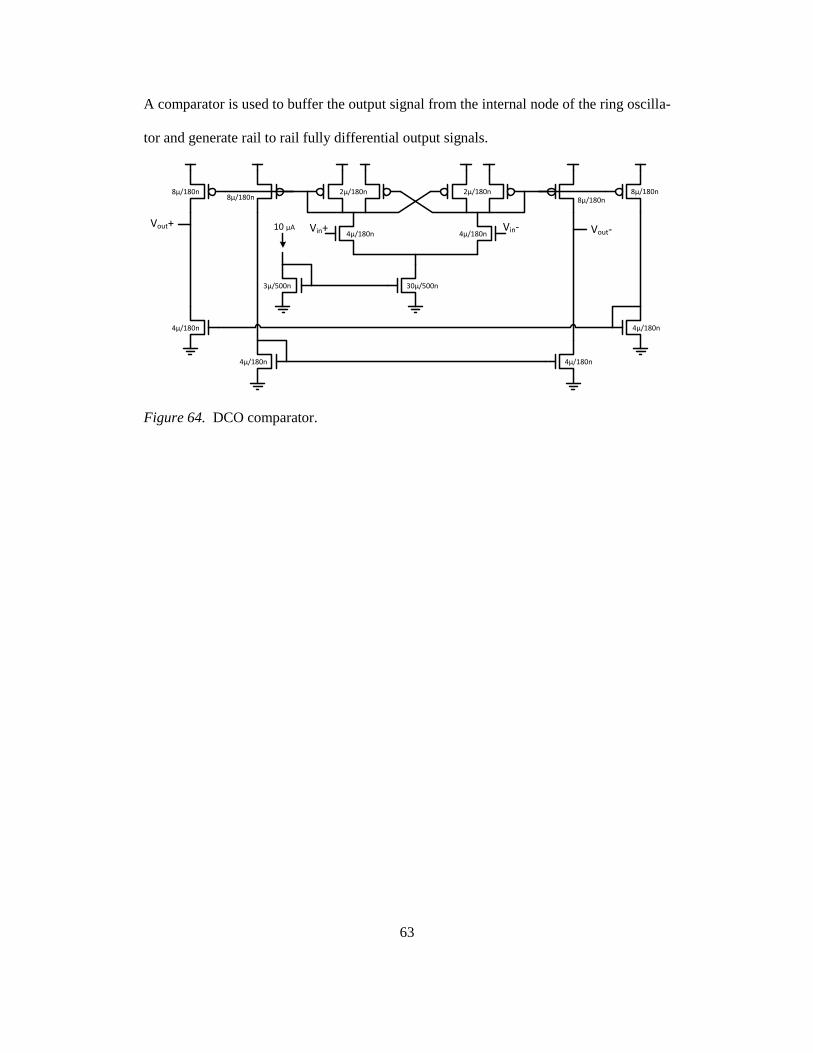
63
A comparator is used to buffer the output signal from the internal node of the ring oscilla-
tor and generate rail to rail fully differential output signals.
Vin+ Vin-Vout+ Vout-4µ/180n 4µ/180n
2µ/180n 2µ/180n8µ/180n
8µ/180n8µ/180n
8µ/180n
30µ/500n3µ/500n
4µ/180n
4µ/180n 4µ/180n
4µ/180n
10 µA
Figure 64. DCO comparator.
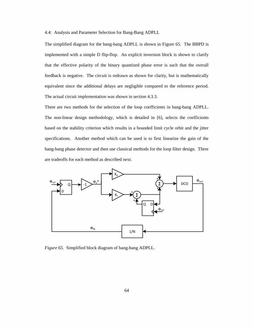
64
4.4: Analysis and Parameter Selection for Bang-Bang ADPLL
The simplified diagram for the bang-bang ADPLL is shown in Figure 65. The BBPD is
implemented with a simple D flip-flop. An explicit inversion block is shown to clarify
that the effective polarity of the binary quantized phase error is such that the overall
feedback is negative. The circuit is redrawn as shown for clarity, but is mathematically
equivalent since the additional delays are negligible compared to the reference period.
The actual circuit implementation was shown in section 4.3.3.
There are two methods for the selection of the loop coefficients in bang-bang ADPLL.
The non-linear design methodology, which is detailed in [6], selects the coefficients
based on the stability criterion which results in a bounded limit cycle orbit and the jitter
specifications. Another method which can be used is to first linearize the gain of the
bang-bang phase detector and then use classical methods for the loop filter design. There
are tradeoffs for each method as described next.
Фref
Фfb
Фout
Kp
KI
Q
D∑
∑
1/N
DCOФe*-1
Фref
Q D
+
+
+
+
Figure 65. Simplified block diagram of bang-bang ADPLL.
65
4.4.1: Non-Linear Analysis and Design
In the derivations ahead, it is sometimes more convenient to use the DCO period
gain, , instead of the DCO frequency gain, . This approximation is derived
in [6] and used throughout in the following derivations:
As discussed in [6] and [12], due to the binary nature of the phase detector and the quan-
tization noise, there will be a steady state limit cycle when the BBPLL is in phase lock.
The analysis done in [6] determines the stability criterion for the bang-bang PLL to lock
into a bounded orbit:
Here, D is the delay through the controller and DCO normalized to the reference period,
and KI and KP are the gains on the integral and proportional paths, respectively. The limit
cycle is a fluctuation of the output frequency around the target frequency which translates
to jitter on the output clock signal. The peak to peak jitter based on the design parameters
is derived:
[
]
One important thing to note from these equations is that with a fixed proportional gain
and delay, increasing the integral path gain will always increase the jitter. Based on the
above equations, the optimal proportional path gain is derived in [6] which minimizes the
peak to peak jitter due to the limit cycle:
(28)
(29)
(31)
(32)
(30)
(27)
66
For this particular design, the proportional path gain, KP, was set to 4 and the integral
path gain, KI, was set to 1 which results in a good tradeoff between jitter and phase and
acquisition time as shown in the results in Chapter 5. The loop parameters were chosen
based on maximum output limit cycle jitter and a bounded orbit in the phase plane, as
described in [6]. The system is assumed to be operating in the limit cycle regime, mean-
ing the limit cycle is dominant over any other noise source in the loop. This assumption
is verified and the results in Chapter 5 confirm that the ADPLL is operating in this re-
gime. As described in [45], any noise source which is dominant over this limit cycle will
scramble the BBPD quantization noise and the power is spread in frequency. This is typ-
ically the case where a much smaller DCO quantization step, , is used along
with a noisy reference clock, as is typically the case in CDRs, or a noisy DCO. Although
it is not the design method used for this implementation, the linearized analysis and de-
sign method is described next for completeness.
[40] performs a similar analysis to describe the non-linear dynamics and also gives a
model for the BBPD from which jitter tracking performance and recovered clock spec-
trum can be derived. As shown in Figure 66, the 2nd
order loop is rearranged to uncover a
sigma-delta modulator acting on the frequency error. Under this delta-sigma approxima-
tion for the inner bang-bang loop, the BBPD can be replaced with a wide-band unity gain
block and the quantization noise has the same characteristics as a random binary bit
stream. This linearized model approximates the behavior of the outer frequency tracking
loop, but does not take into account the extra tracking of the non-linear delta-sigma core.
This analysis also requires the loop is not slew rate limiting or in a periodic limit cycle,
which assumes the VCO phase noise is dominant in the loop.
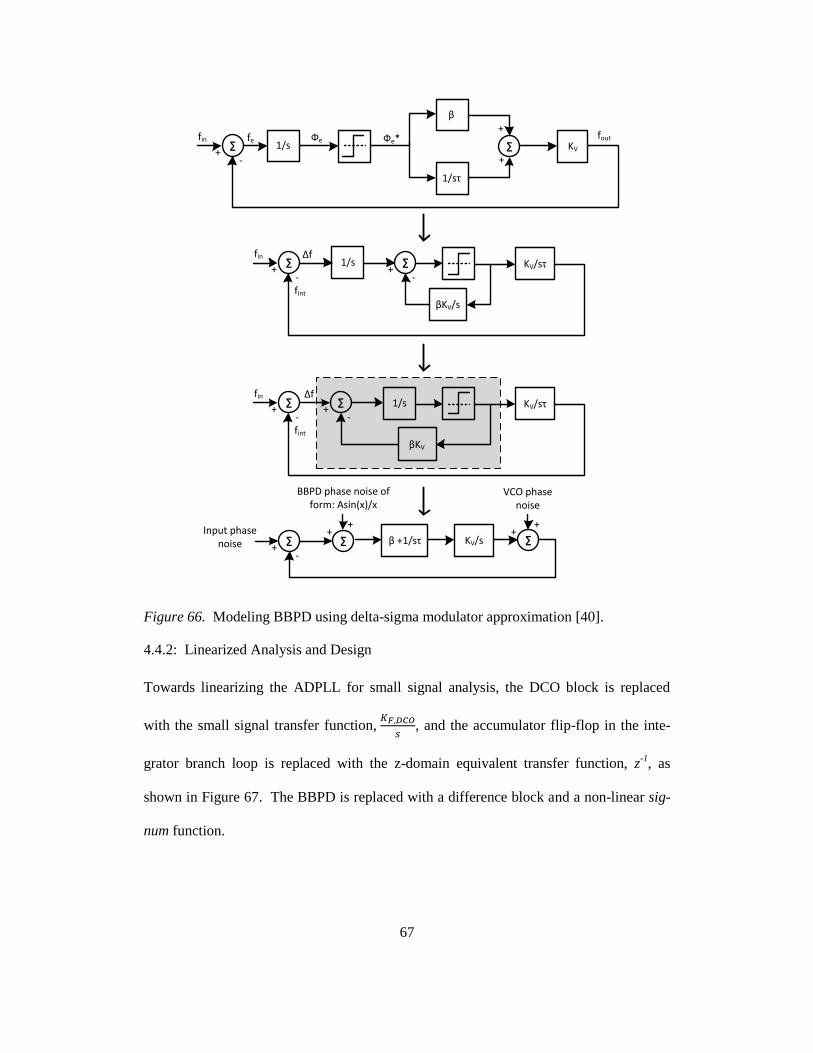
67
fin fout
β
1/sτ
∑ Фe
∑ +
-
Фe*
+
+
KV 1/s fe
fin
fint
βKV/s
∑ +
-KV/sτ1/s
∆f∑
+-
fin
fint
βKV
∑ +
-KV/sτ1/s
∆f∑
+-
β +1/sτ ∑ +
-
KV/s∑ +
∑ +
+ +
VCO phase noise
BBPD phase noise of form: Asin(x)/x
Input phase noise
Figure 66. Modeling BBPD using delta-sigma modulator approximation [40].
4.4.2: Linearized Analysis and Design
Towards linearizing the ADPLL for small signal analysis, the DCO block is replaced
with the small signal transfer function,
, and the accumulator flip-flop in the inte-
grator branch loop is replaced with the z-domain equivalent transfer function, z-1
, as
shown in Figure 67. The BBPD is replaced with a difference block and a non-linear sig-
num function.
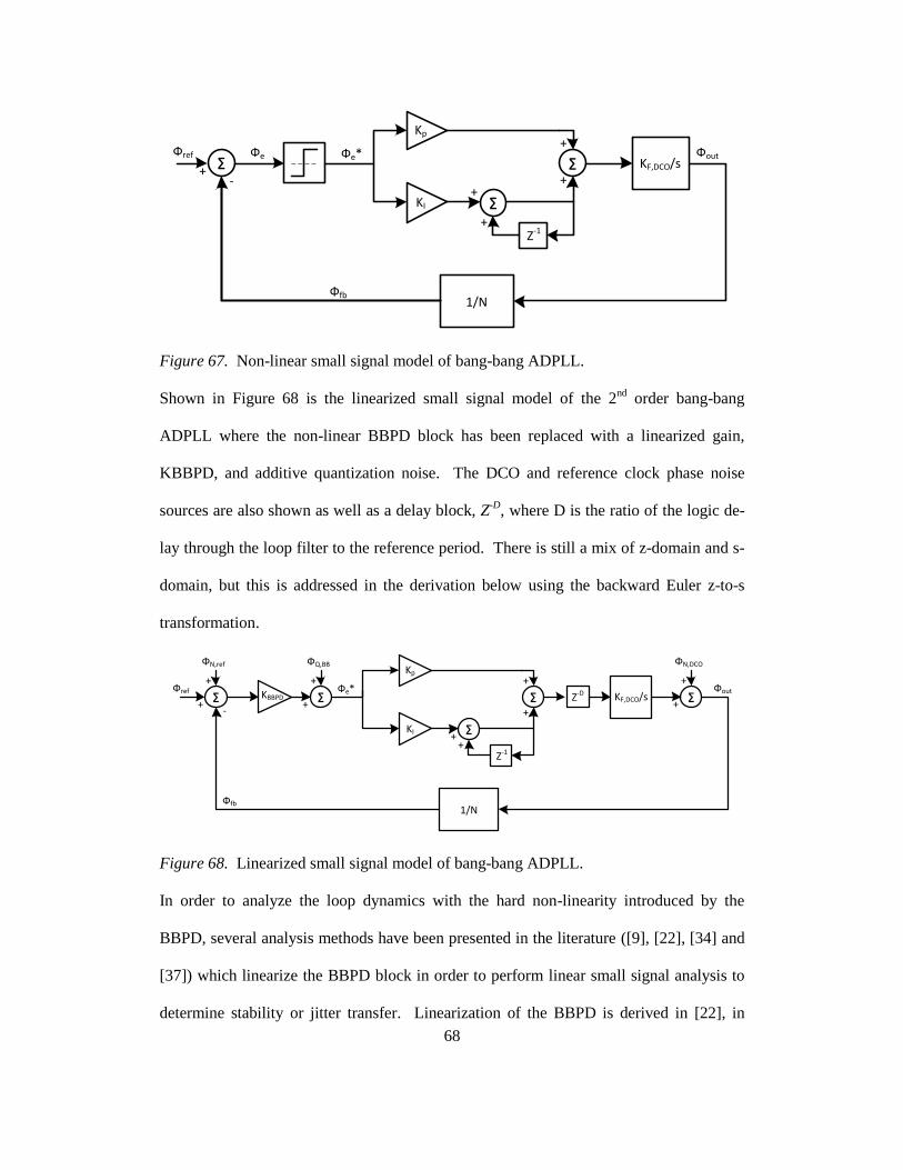
68
Фref
Фfb
Фout
Kp
KI
Z-1
∑
∑ Фe
1/N
KF,DCO/s∑ +
-
Фe*
+
+
+
+
Figure 67. Non-linear small signal model of bang-bang ADPLL.
Shown in Figure 68 is the linearized small signal model of the 2nd
order bang-bang
ADPLL where the non-linear BBPD block has been replaced with a linearized gain,
KBBPD, and additive quantization noise. The DCO and reference clock phase noise
sources are also shown as well as a delay block, Z-D
, where D is the ratio of the logic de-
lay through the loop filter to the reference period. There is still a mix of z-domain and s-
domain, but this is addressed in the derivation below using the backward Euler z-to-s
transformation.
Фref
Фfb
Фout
Kp
KI
Z-1
∑
∑ Фe*
1/N
KF,DCO/s∑ +
-
++
KBBPD ∑
ФQ,BB
+
+ +
+
ФN,ref
+
∑
ФN,DCO
+
+
Z-D
Figure 68. Linearized small signal model of bang-bang ADPLL.
In order to analyze the loop dynamics with the hard non-linearity introduced by the
BBPD, several analysis methods have been presented in the literature ([9], [22], [34] and
[37]) which linearize the BBPD block in order to perform linear small signal analysis to
determine stability or jitter transfer. Linearization of the BBPD is derived in [22], in
69
which the linear region of the BBPD transfer curve is due to the metastability of the
latches used and requires knowledge of the latch regeneration time as well as other inter-
nal parameters that are not typically available in standard cells. In [9] the bang-bang
phase detector gain is derived using Markov chains and the assumption of a Gaussian
distributed reference jitter as well as a noise-free DCO:
√ [
(
)
]
If the reference clock jitter, , is much greater then the DCO quantization step,
, this simplifies to
√
This is typically the case with CDRs since the input clock is actually a random bit
sequence which is noisier than the DCO. The opposite is true in the case of frequency
synthesizers since a low phase noise reference clock is used and the DCO quantization
step is greater than the input reference jitter. Under this assumption, the phase detector
gain is approximated as
√
One assumption in this derivation is that the loop is first order or second order with a
proportional gain much greater than the integral gain. A similar derivation is performed
in [34] which also assumes a Guassian distribution of reference clock jitter. Both of these
derivations are useful in analysis of ADPLLs used in CDRs.
It is useful to determine the phase detector gain dependence on DCO jitter. [45] analyzes
the linearized BBPD gain dependence on DCO jitter. This work also discusses maximum
DCO resolution to jitter ratio which removes the limit cycle. This work derives the
BBPD gain as:
(33)
(35)
(34)
70
√
√
√
√
√ (
√
√
√ )
A similar investigation is performed in [37], where a closed form analytic expression as
well as asymptotic solutions to the phase detector gain are derived at small and large
DCO jitter extremes. As the DCO jitter, , approaches infinity:
As the DCO jitter, , approaches zero:
These results show a small difference due to the assumption of Gaussian distribution of
DCO jitter components in [37]. For sufficiently small DCO jitter, the loop dynamics will
be nonlinear, and a linear analysis cannot be applied [8][45]. These results are particular-
ly useful in the analysis of ADPLLs with binary phase detectors used for frequency syn-
thesis since the DCO jitter as well as the overload and hunting jitter due to the BBPD
dominate over the reference clock jitter [37].
To summarize the results from the literature, linearized BBPD gain is inversely propor-
tional to the input reference clock jitter as well the DCO jitter. As DCO jitter increases,
the gain fairly constant and inversely proportional to the DCO quantization step, NKPKT
and as DCO jitter tends towards infinity, the BBPD gain is inversely proportional to the
square of the DCO jitter. With a clean reference clock, however, and with a sufficiently
low DCO jitter, the loop dynamics are non-linear and the behavior can be analyzed with a
non-linear map as described in [6]. [8] gives a threshold for input jitter to DCO quantiza-
(39)
(40)
()
(36)
(37)
(38)
71
tion step ratio, , below which results in non-linear behavior, and above which linear
analysis is appropriate.
Once the BBPD linearized gain is determined, the traditional analysis of the loop can be
performed. The digital loop filter is modeled by the phase error to DCO control word
transfer function:
(
)
In order to analyze the small signal behavior, it is convenient to work entirely in the
Lapace domain. It is therefore necessary to perform the z-to-s transformation of the loop
filter transfer function:
| (
) ( )
The z-to-s transformation is performed using the backward Euler approximation, which is
reasonable since is typically very small at frequencies of interest. The DCO is
modeled as an ideal phase integrator similar to the analog PLL case:
The ADPLL forward gain is then computed by all the gain terms in the forward path:
(
)( )
The gain in the feedback loop, or reverse gain, is due to the feedback frequency divider:
The loop gain is the gain from the non-inverting input of the phase detector back to the
inverting input of the phase detector and is sometimes called the open loop gain:
(45)
(46)
(44)
(42)
(43)
(41)
72
(
)( )
The closed loop gain is derived just as in classic linear feedback system analysis:
(
)( )
(
)( )
Using the assumption that
(
)
(
)
For the standard 2nd
order PLL, the s-domain signal TF is
(
)
(
)
From this derivation, it can be seen that the z-to-s transformed signal transfer function is
of the same form as the continuous time signal transfer function which is used in the de-
sign of charge pump based PLLs. Once the linearized gain of the BBPD is calculated
based on the knowledge of DCO or reference jitter, a procedure similar to that discussed
in section 2.4.1 can be used to select the digital filter loop coefficients such that the re-
quired loop bandwidth and phase margin are met. [21] details the CPPLL design proce-
dure as well as a procedure to migrate from a CPPLL to ADPLL.
As mentioned in section 3.2, there is quantization noise due to the discrete nature of time
to digital conversion and digital to frequency conversion in the DCO. These quantization
noise sources can be estimated as described in [26], which describe an ADPLL system
similar to that described in [35] and [36]. The in-band phase noise estimation is given in
Equation 52.
(47)
(48)
(49)
(50)
(51)
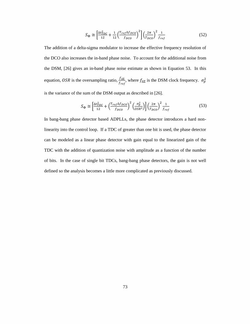
73
[
(
)
] (
)
The addition of a delta-sigma modulator to increase the effective frequency resolution of
the DCO also increases the in-band phase noise. To account for the additional noise from
the DSM, [26] gives an in-band phase noise estimate as shown in Equation 53. In this
equation, is the oversampling ratio,
, where is the DSM clock frequency.
is the variance of the sum of the DSM output as described in [26].
[
(
)
(
)] (
)
In bang-bang phase detector based ADPLLs, the phase detector introduces a hard non-
linearity into the control loop. If a TDC of greater than one bit is used, the phase detector
can be modeled as a linear phase detector with gain equal to the linearized gain of the
TDC with the addition of quantization noise with amplitude as a function of the number
of bits. In the case of single bit TDCs, bang-bang phase detectors, the gain is not well
defined so the analysis becomes a little more complicated as previously discussed.
(52)
(53)
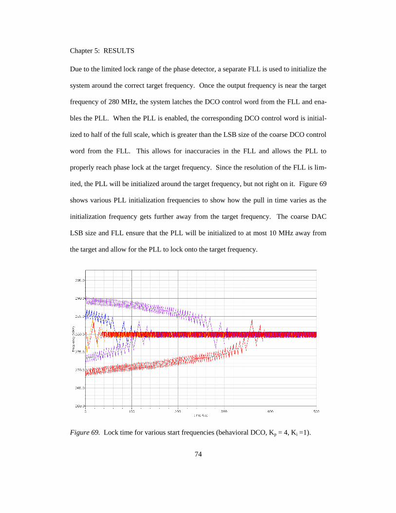
74
Chapter 5: RESULTS
Due to the limited lock range of the phase detector, a separate FLL is used to initialize the
system around the correct target frequency. Once the output frequency is near the target
frequency of 280 MHz, the system latches the DCO control word from the FLL and ena-
bles the PLL. When the PLL is enabled, the corresponding DCO control word is initial-
ized to half of the full scale, which is greater than the LSB size of the coarse DCO control
word from the FLL. This allows for inaccuracies in the FLL and allows the PLL to
properly reach phase lock at the target frequency. Since the resolution of the FLL is lim-
ited, the PLL will be initialized around the target frequency, but not right on it. Figure 69
shows various PLL initialization frequencies to show how the pull in time varies as the
initialization frequency gets further away from the target frequency. The coarse DAC
LSB size and FLL ensure that the PLL will be initialized to at most 10 MHz away from
the target and allow for the PLL to lock onto the target frequency.
Figure 69. Lock time for various start frequencies (behavioral DCO, Kp = 4, Ki =1).
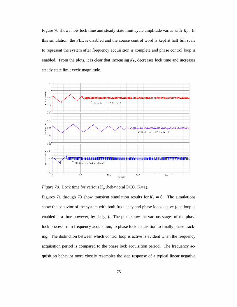
75
Figure 70 shows how lock time and steady state limit cycle amplitude varies with . In
this simulation, the FLL is disabled and the coarse control word is kept at half full scale
to represent the system after frequency acquisition is complete and phase control loop is
enabled. From the plots, it is clear that increasing , decreases lock time and increases
steady state limit cycle magnitude.
Figure 70. Lock time for various Kp (behavioral DCO, Ki=1).
Figures 71 through 73 show transient simulation results for . The simulations
show the behavior of the system with both frequency and phase loops active (one loop is
enabled at a time however, by design). The plots show the various stages of the phase
lock process from frequency acquisition, to phase lock acquisition to finally phase track-
ing. The distinction between which control loop is active is evident when the frequency
acquisition period is compared to the phase lock acquisition period. The frequency ac-
quisition behavior more closely resembles the step response of a typical linear negative
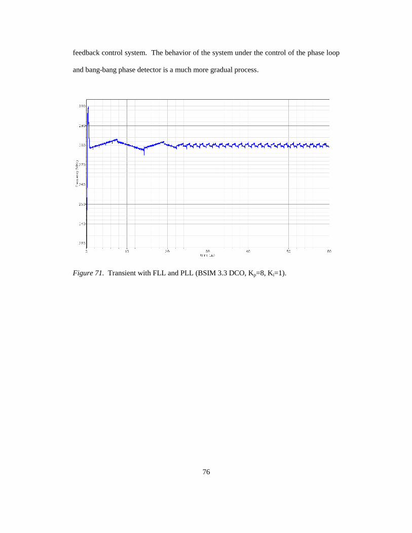
76
feedback control system. The behavior of the system under the control of the phase loop
and bang-bang phase detector is a much more gradual process.
Figure 71. Transient with FLL and PLL (BSIM 3.3 DCO, Kp=8, Ki=1).
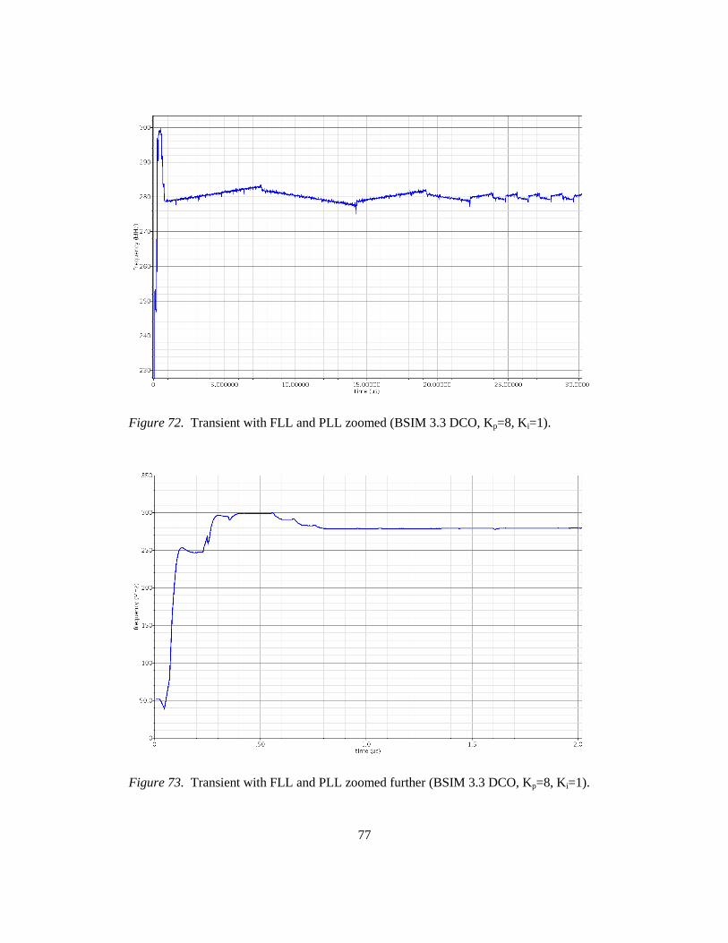
77
Figure 72. Transient with FLL and PLL zoomed (BSIM 3.3 DCO, Kp=8, Ki=1).
Figure 73. Transient with FLL and PLL zoomed further (BSIM 3.3 DCO, Kp=8, Ki=1).
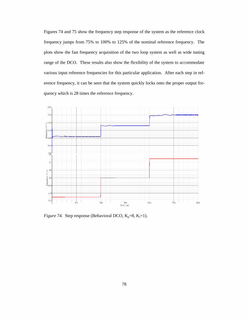
78
Figures 74 and 75 show the frequency step response of the system as the reference clock
frequency jumps from 75% to 100% to 125% of the nominal reference frequency. The
plots show the fast frequency acquisition of the two loop system as well as wide tuning
range of the DCO. These results also show the flexibility of the system to accommodate
various input reference frequencies for this particular application. After each step in ref-
erence frequency, it can be seen that the system quickly locks onto the proper output fre-
quency which is 28 times the reference frequency.
Figure 74. Step response (Behavioral DCO, Kp=8, Ki=1).
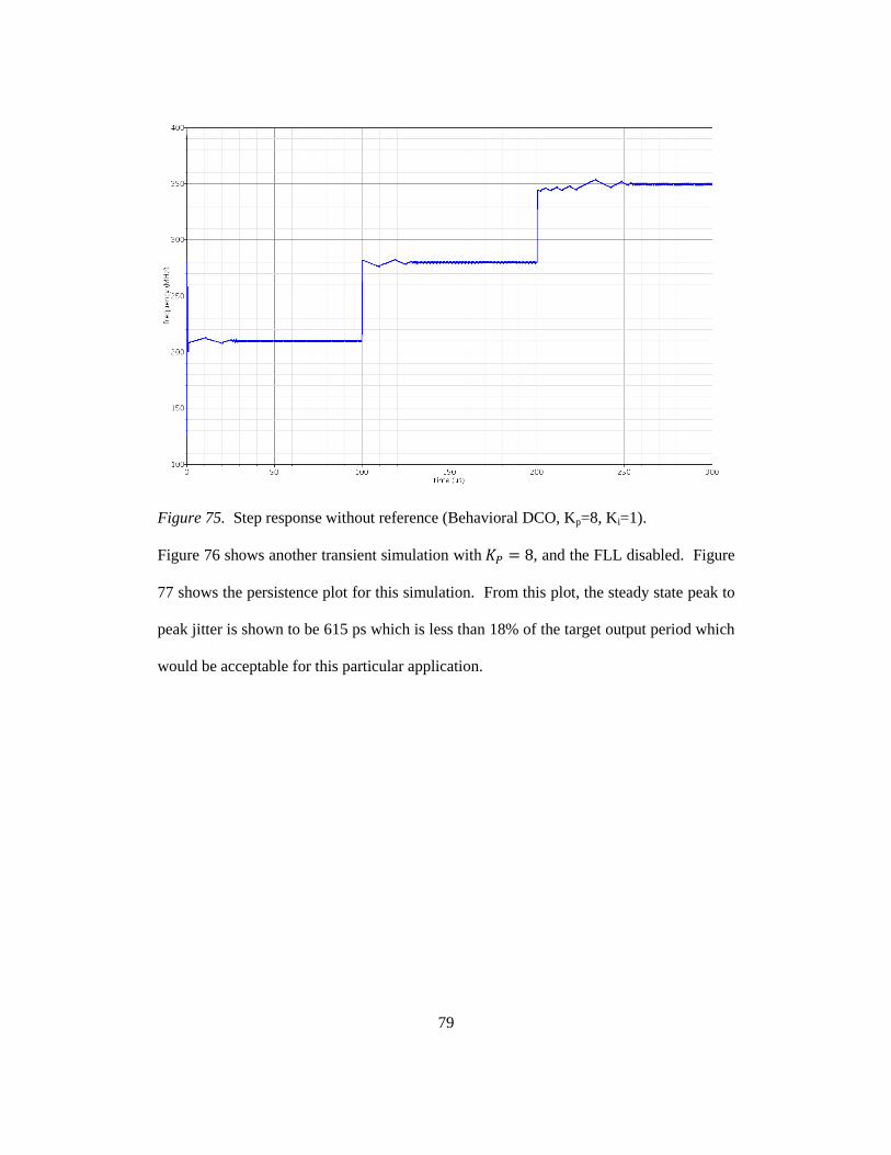
79
Figure 75. Step response without reference (Behavioral DCO, Kp=8, Ki=1).
Figure 76 shows another transient simulation with , and the FLL disabled. Figure
77 shows the persistence plot for this simulation. From this plot, the steady state peak to
peak jitter is shown to be 615 ps which is less than 18% of the target output period which
would be acceptable for this particular application.
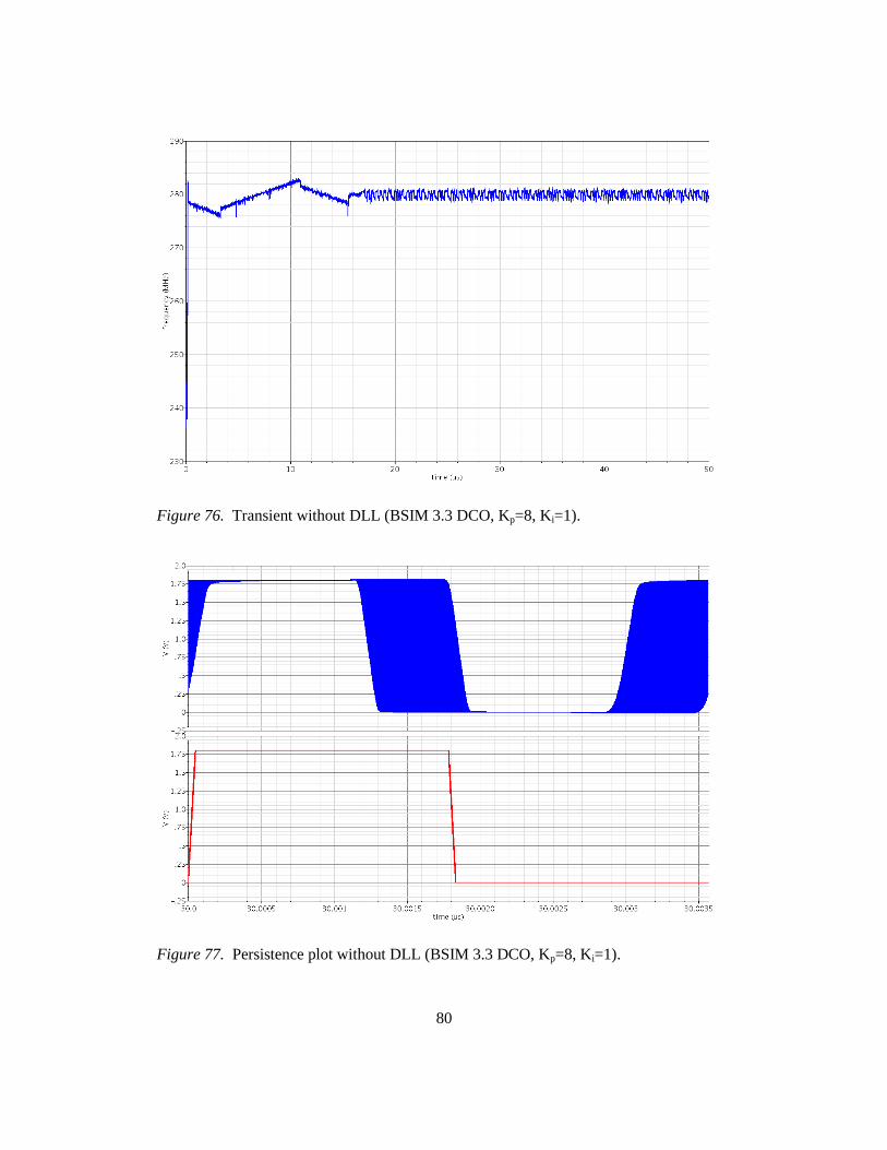
80
Figure 76. Transient without DLL (BSIM 3.3 DCO, Kp=8, Ki=1).
Figure 77. Persistence plot without DLL (BSIM 3.3 DCO, Kp=8, Ki=1).
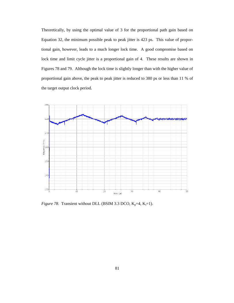
81
Theoretically, by using the optimal value of 3 for the proportional path gain based on
Equation 32, the minimum possible peak to peak jitter is 423 ps. This value of propor-
tional gain, however, leads to a much longer lock time. A good compromise based on
lock time and limit cycle jitter is a proportional gain of 4. These results are shown in
Figures 78 and 79. Although the lock time is slightly longer than with the higher value of
proportional gain above, the peak to peak jitter is reduced to 380 ps or less than 11 % of
the target output clock period.
Figure 78. Transient without DLL (BSIM 3.3 DCO, Kp=4, Ki=1).
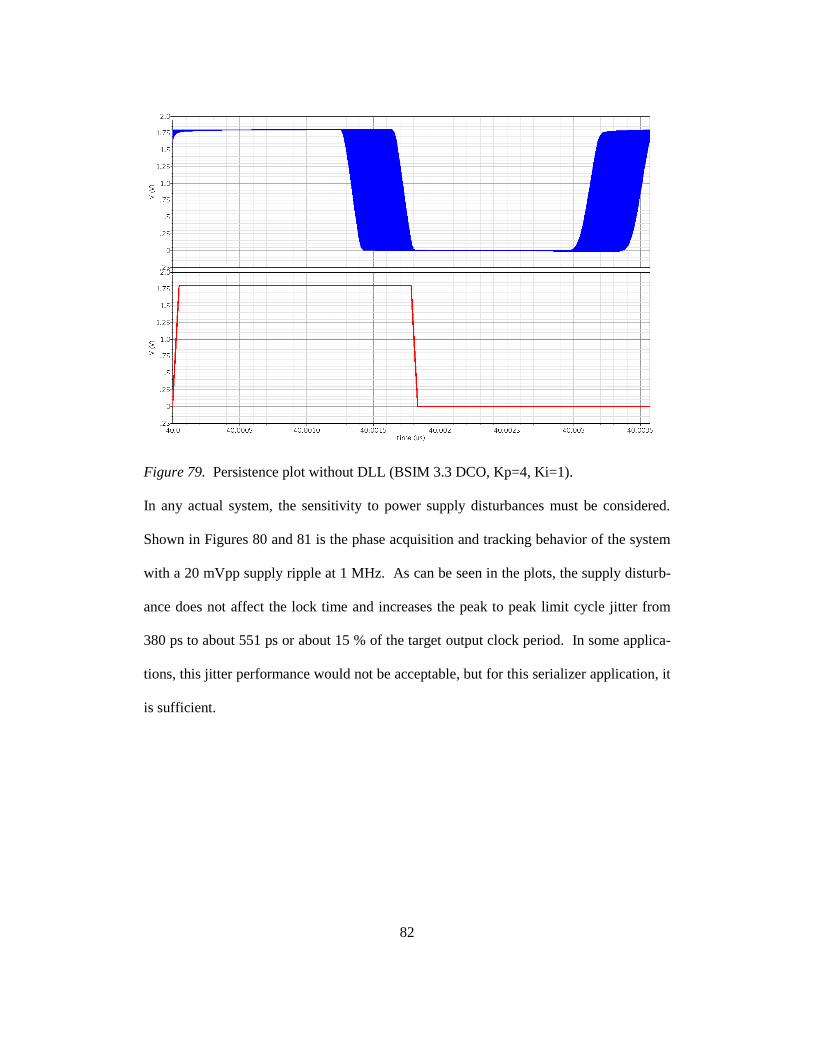
82
Figure 79. Persistence plot without DLL (BSIM 3.3 DCO, Kp=4, Ki=1).
In any actual system, the sensitivity to power supply disturbances must be considered.
Shown in Figures 80 and 81 is the phase acquisition and tracking behavior of the system
with a 20 mVpp supply ripple at 1 MHz. As can be seen in the plots, the supply disturb-
ance does not affect the lock time and increases the peak to peak limit cycle jitter from
380 ps to about 551 ps or about 15 % of the target output clock period. In some applica-
tions, this jitter performance would not be acceptable, but for this serializer application, it
is sufficient.
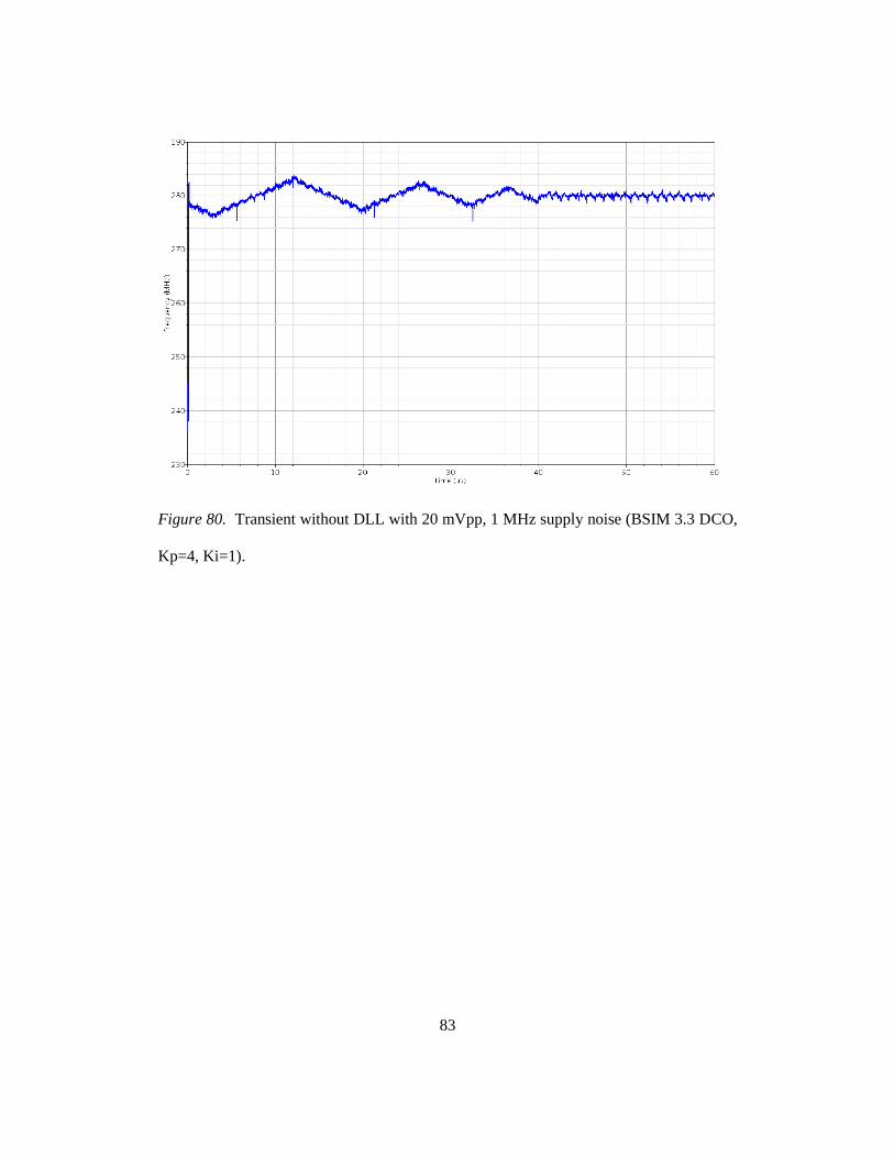
83
Figure 80. Transient without DLL with 20 mVpp, 1 MHz supply noise (BSIM 3.3 DCO,
Kp=4, Ki=1).
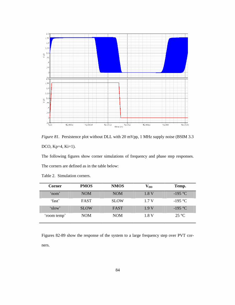
84
Figure 81. Persistence plot without DLL with 20 mVpp, 1 MHz supply noise (BSIM 3.3
DCO, Kp=4, Ki=1).
The following figures show corner simulations of frequency and phase step responses.
The corners are defined as in the table below:
Table 2. Simulation corners.
Corner PMOS NMOS VDD Temp.
‘nom’ NOM NOM 1.8 V -195 °C
‘fast’ FAST SLOW 1.7 V -195 °C
‘slow’ SLOW FAST 1.9 V -195 °C
‘room temp’ NOM NOM 1.8 V 25 °C
Figures 82-89 show the response of the system to a large frequency step over PVT cor-
ners.
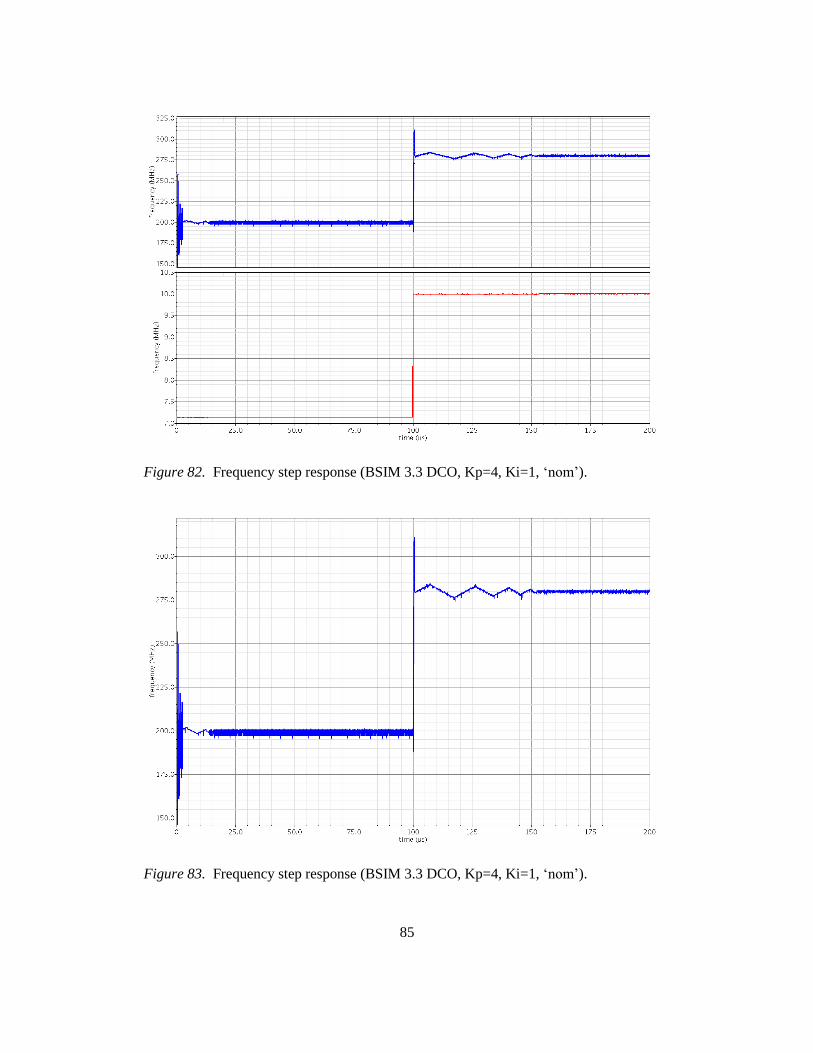
85
Figure 82. Frequency step response (BSIM 3.3 DCO, Kp=4, Ki=1, ‘nom’).
Figure 83. Frequency step response (BSIM 3.3 DCO, Kp=4, Ki=1, ‘nom’).
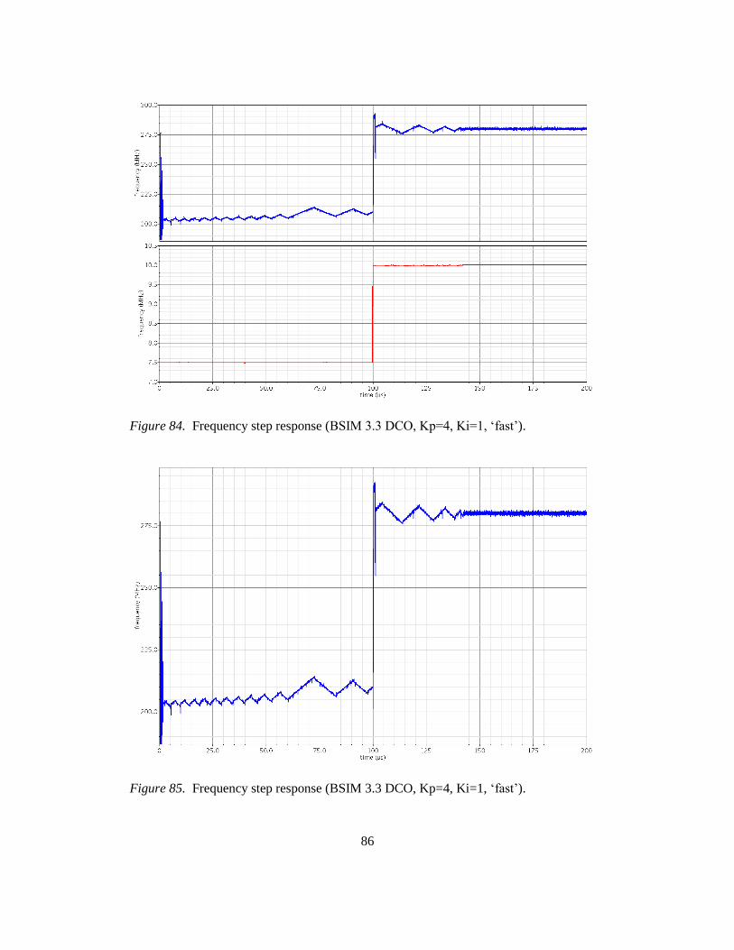
86
Figure 84. Frequency step response (BSIM 3.3 DCO, Kp=4, Ki=1, ‘fast’).
Figure 85. Frequency step response (BSIM 3.3 DCO, Kp=4, Ki=1, ‘fast’).
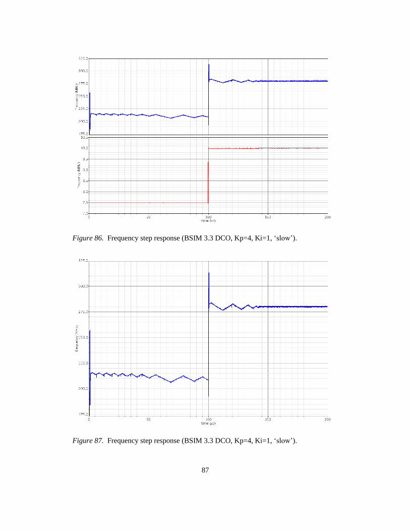
87
Figure 86. Frequency step response (BSIM 3.3 DCO, Kp=4, Ki=1, ‘slow’).
Figure 87. Frequency step response (BSIM 3.3 DCO, Kp=4, Ki=1, ‘slow’).
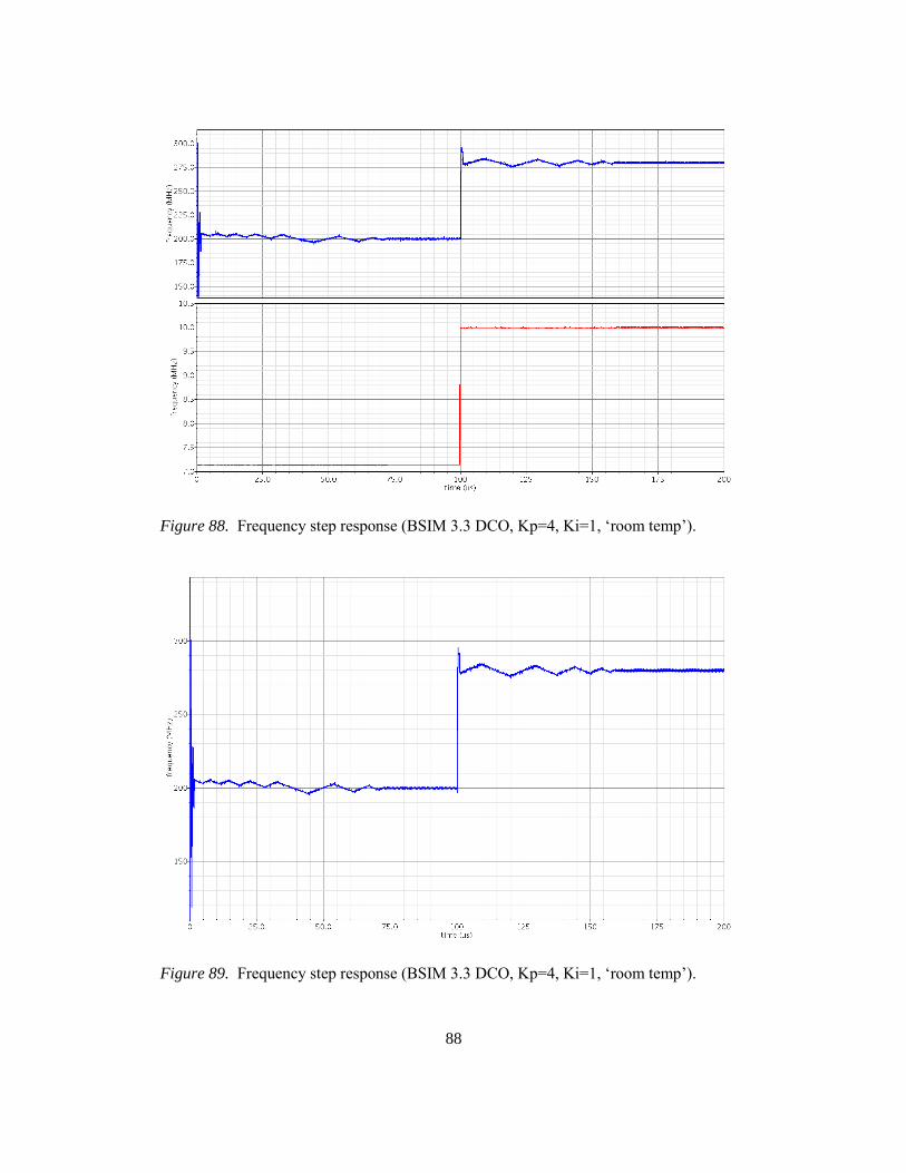
88
Figure 88. Frequency step response (BSIM 3.3 DCO, Kp=4, Ki=1, ‘room temp’).
Figure 89. Frequency step response (BSIM 3.3 DCO, Kp=4, Ki=1, ‘room temp’).
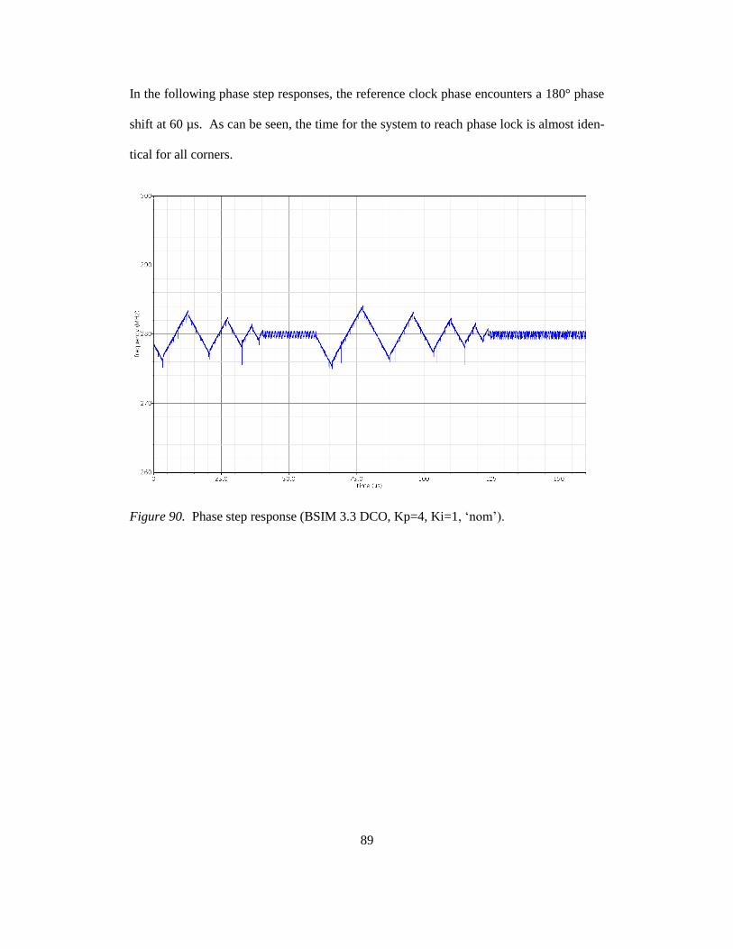
89
In the following phase step responses, the reference clock phase encounters a 180° phase
shift at 60 µs. As can be seen, the time for the system to reach phase lock is almost iden-
tical for all corners.
Figure 90. Phase step response (BSIM 3.3 DCO, Kp=4, Ki=1, ‘nom’).
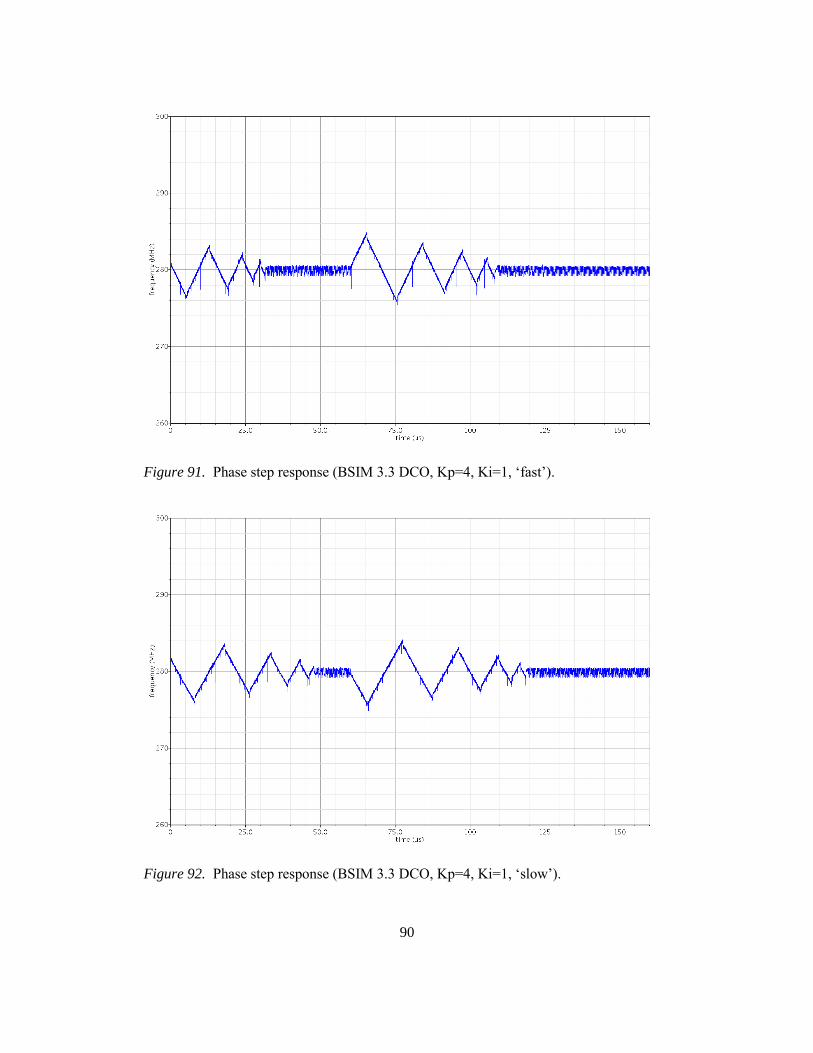
90
Figure 91. Phase step response (BSIM 3.3 DCO, Kp=4, Ki=1, ‘fast’).
Figure 92. Phase step response (BSIM 3.3 DCO, Kp=4, Ki=1, ‘slow’).
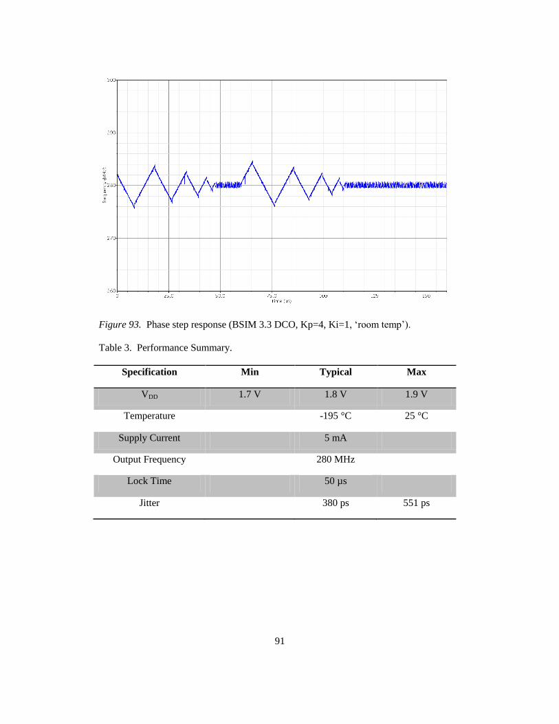
91
Figure 93. Phase step response (BSIM 3.3 DCO, Kp=4, Ki=1, ‘room temp’).
Table 3. Performance Summary.
Specification Min Typical Max
VDD 1.7 V 1.8 V 1.9 V
Temperature -195 °C 25 °C
Supply Current 5 mA
Output Frequency 280 MHz
Lock Time 50 µs
Jitter 380 ps 551 ps
92
Chapter 6: CONCLUSION
6.1: Conclusion
A digitally intensive phase locked loop system has been designed in 180 nm CMOS pro-
cess. This implementation is intended for use as a clock multiplier in a PISO to interface
with 2 14-bit ADCs. The design utilizes a binary, or bang-bang, phase detector and fre-
quency detector to achieve 380 ps jitter with 9 mW power consumption from a 1.8 V
supply. The PLL also has a tuning range of about 300 MHz with a dynamic range of
about 73 dB for about 12 effective bits of resolution. The design allows for easy reuse in
that the loop coefficients can be programmed based on the required system bandwidth
and dynamic requirements. Not only can the loop coefficients be adjusted, but the multi-
plier factor can be changed with ease. The design is highly digital with the DCO consist-
ing of custom analog blocks with elements available in most deep sub-micron CMOS
processes.
6.2: Future Work
6.2.1: Layout and Verification
As of this writing, the design is still in the layout phase. Following the physical design
and LVS, parasitic extraction and post-layout simulation will be performed. Pre and
post-layout simulation results will be compared and the design will be taped out if there
are no major discrepancies.
To further prove functionality of the ADPLL in this specific application, a simulation
with the PISO is also necessary. Various data sequences should be clocked in at the input
of the PISO and the serial output should be measured relative to an ideal clock at 280
93
MHz. The data output, as well as the other clock outputs of the PISO need to be checked
to ensure timing specs are met over the PVT corners mentioned above.
The DCO is the most analog intensive block and non-idealities within it could have an
impact on the PLL performance if not looked at closely. The current mode DAC INL
will most likely affect the frequency acquisition process because of the larger LSB size of
the coarse loop and multibit operation. DNL will likely contribute to phase acquisition
and phase tracking since the phase control loop operates in much smaller frequency steps
compared to the frequency control loop. Glitching may also affect the PLL loop dynam-
ics. Monte Carlo simulations may prove helpful in unearthing some effects of these non-
idealities if the parameters are chosen appropriately. The parameters will be chosen
based on which has the biggest impact on timing variation, glitching, and non-linearity.
So far, only the jitter caused by the bang-bang phase detector limit cycle, DAC glitches
and quantization noise from the digital controllers has been analyzed. Noise analysis
may be performed in the time domain using the transient noise option in Spectre. Anoth-
er option for a more accurate jitter simulation is by using pss/pnoise in jitter mode in
Spectre RF.
6.2.2: Post Silicon Validation
An evaluation board and test plan will be developed to test the design under room tem-
perature and cryogenic conditions. An FPGA or microcontroller can be used to send par-
allel data to the serializer and receive serial data from the serializer. A stable 10 MHz
clock signal will also be required which will be generated by a crystal oscillator. The
serializer and oscillator will need to be separate from the FPGA/microcontroller board so
testing can be performed under room temperature as well as cryogenic conditions and
most FPGA/microcontrollers are not designed to be operated under such conditions.
94
One option for testing the ADPLL and serializer is shown in Figure 94. As shown, there
can be two options for the input to the serializer which can be selected via software or
switches on the evaluation board. One option is to use two 14-bit ADCs clocked at 10
MHz to convert low frequency analog signal waveforms from a function generator which
would replicate conditions similar to that of the end application. The other option is to
generate digital vectors within the µC/FPGA core to be shipped out to the serializer in
sync with the 10 MHz oscillator.
The serializer output data would be fed back to the µC/FPGA core and SIPO function
performed and the serializer input data could then be compared with this data. The out-
put of the SIPO, if the serializer and ADPLL were functional, should simply be a delayed
version of the serializer input data. These tests could be performed under room tempera-
ture conditions as well as cryogenic conditions by enclosing the daughter board contain-
ing the ADPLL and serializer in a cryogenically cooled dewar.
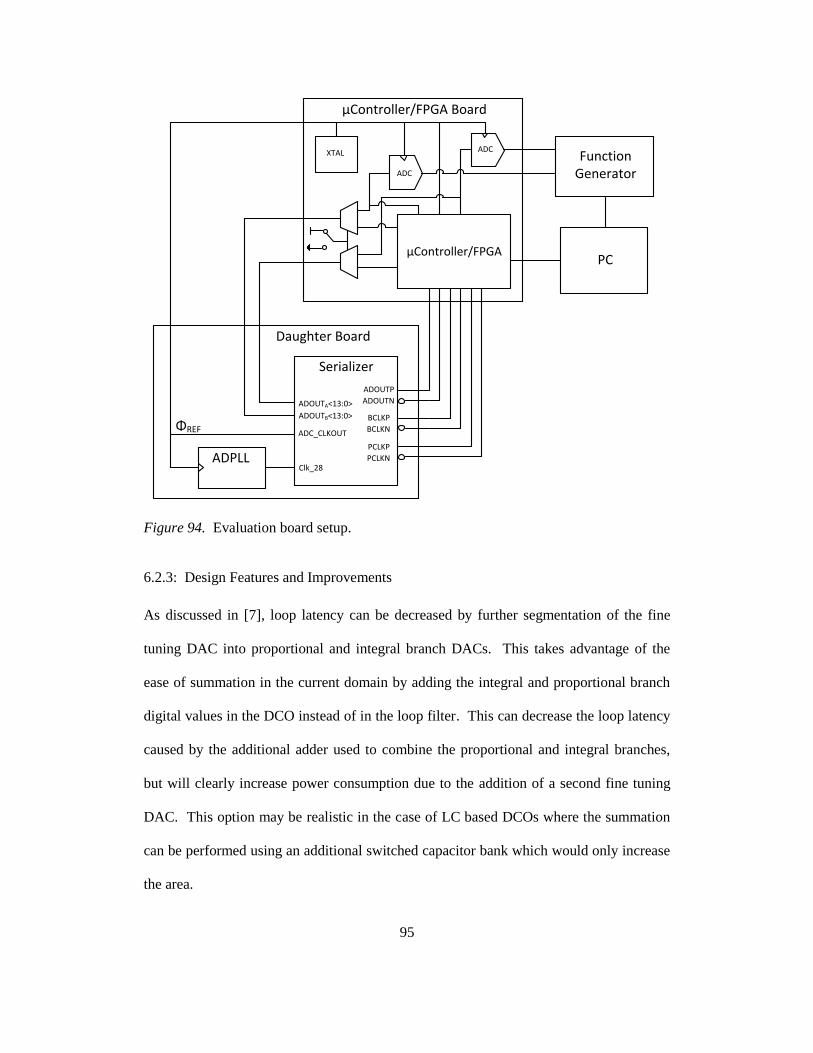
95
ΦREF
Serializer
ADPLLClk_28
PCLKN
PCLKP
BCLKN
BCLKP
ADOUTN
ADOUTP
ADC_CLKOUT
ADOUTA<13:0>
ADOUTB<13:0>
µController/FPGA Board
Function Generator
PC
XTAL
µController/FPGA
ADC
ADC
Daughter Board
Figure 94. Evaluation board setup.
6.2.3: Design Features and Improvements
As discussed in [7], loop latency can be decreased by further segmentation of the fine
tuning DAC into proportional and integral branch DACs. This takes advantage of the
ease of summation in the current domain by adding the integral and proportional branch
digital values in the DCO instead of in the loop filter. This can decrease the loop latency
caused by the additional adder used to combine the proportional and integral branches,
but will clearly increase power consumption due to the addition of a second fine tuning
DAC. This option may be realistic in the case of LC based DCOs where the summation
can be performed using an additional switched capacitor bank which would only increase
the area.
96
Decreasing power consumption is always of importance. In this implementation, the
DAC is the primary source of power consumption. Future design revisions may address
this issue by using a separate lower voltage rail for the DAC. The DAC is a wide-swing
cascode based design which allows for a lower supply voltage, but the lower limit to the
supply has yet to be determined. Other studies may also need to be performed which as-
sess the tradeoffs between linearity and power based on unit current source sizes and op-
eration in subthreshold region.
Another possible improvement would be to make the frequency divider more program-
mable. The feedback divider is designed such that it can modified to accommodate any
even integer divide ratio up to a 2N where N is the number of flip flops in the divider. In
the current implementation, the divide ratio is fixed at 28, which is determined by the
counter reset logic as shown in Figure 47. As can be seen in the figure, the outputs of the
flip flops are used to determine the count and when the count reaches 13, the counter is
reset to 0. The MSB of this counter goes to another divide by two such that the output
frequency of the final flip flop is the input frequency divided by 28, which is 2(M+1),
where M is the reset count. The divide ratio, 28 here, is used as the FCW in the frequen-
cy control loop giving the relationship FCW = 2(M+1). In this implementation, M is
hardcoded in the logic using and gates, however, M can be set using a digital code and
additional logic allowing for any even number divider ratio.
Since the steady state jitter on the output is an increasing function of the fine phase loop
DAC LSB size. Increasing the resolution of the fine DAC in the phase control loop will
accomplish this, however at a power penalty. Delta-sigma modulation of the fine DAC
LSBs is one way to accomplish higher resolution while only marginally increasing the
power consumption. This is very similar to the method used in fractional-N PLLs where
97
the divide ratio is switched back and forth between two ratios such that the effective ratio
is a fraction between the two divider ratios in the programmable divider.
Linearity of the DAC is very important and in order to minimize the DNL, mismatch of
the current sources in the binary weighted arrays needs to be minimized. One way to do
this is by dynamic element matching. This is a process in which the enabled current
sources in the binary array are randomized in time such that the mismatch error is aver-
aged over time. DEM requires oversampling, which is possible by using the oscillator
output clock and realizing that the DAC control word is updated once every 28 output
clock cycles.
The phase loop control parameters KP and KI are hardcoded to 4 and 1 respectively; how-
ever, they can be programmed one time by using fuses or EEPROM based on desired
loop dynamics or jitter requirements. The control parameters can also be controlled dy-
namically with additional locking process monitoring circuitry as described in [42]. Dy-
namically adjusting the loop control parameters can decouple the tradeoff between loop
bandwidth and limit cycle jitter.
PVT variations can be partially compensated for by changing the pedestal current. In the
current implementation, two identical sized current sources are used to provide a pedestal
current of 0, IP and 2IP. These calibration current sources allow for the user to increase or
decrease the center frequency of the DCO by approximately 20 MHz. This is essentially
a 3 level unary weighted current mode DAC, but any resolution binary or unary weighted
current mode DAC could be used. The control word of the pedestal DAC could be con-
trolled by a calibration circuit which is active upon startup or even periodically enabled
during normal operation to adjust the center frequency of the DCO around the proper op-
erating point over PVT corners.
98
As of this writing, the resolution of the FLL is limited to due to the fact that the fre-
quency detection circuit counts DCO output clock edges between reference clock edges
in order to get an indication of the DCO output frequency. The resolution can be in-
creased by increasing the number of reference periods during which the DCO output
clock edges are accumulated and taking the average over the number of periods. The
resolution can effectively be increased to
, where M is the number of reference clock
cycles over which the DCO clock phase is accumulated.
99
REFERENCES
[1] V. Arkesteijn, E. Klumperink, B. Nauta, “Jitter Requirements of the Sampling Clock
in Software Radio Receivers,” IEEE Transactions on Circuits and Systems-II: Ex-
press Briefs, Vol. 53, No. 2, pp.90-94, February 2006.
[2] D. Birru, “A Novel Delay-Locked Loop Based CMOS Clock Multiplier,” IEEE
Transactions on Consumer Electronics, Vol. 44, No. 4, pp.1319-1322, November
1998.
[3] G. Chien, Low-Noise Local Oscillator Design Techniques using a DLL-based Fre-
quency Multiplier for Wireless Applications, PhD Dissertation, University of Califor-
nia, Berkeley, Berkeley, CA, 1999.
[4] J. Crossley, E. Naviaski, E. Alon, “An Energy Efficient Ring-Oscillator Digital PLL,”
IEEE Custom Integrated Circuits Conference, pp. 1-4, 2010.
[5] N. Da Dalt, “Techniques for the Analysis of Digital Bang-Bang PLLs,” Multi-
Mode/Multi-Band RF Transceivers for Wireless Communications, Ch. 16, John
Wiley & Sons, Inc, 2011.
[6] N. Da Dalt, “A Design-Oriented Study of the Nonlinear Dynamics of Digital Bang-
Bang PLLs,” IEEE Transactions on Circuits and Systems-I: Regular Papers, Vol. 52,
No. 1, pp. 21-31, January 2005.
[7] N. Da Dalt, Theory and Implementation of Digital Bang-Bang Frequency Synthesiz-
ers for High Speed Serial Data Communications, PhD Dissertation, RWTH Aachen
University, Aachen, North Rhine-Westphalia, Germany, 2007.
[8] N. Da Dalt, “Linearized Analysis of a Digital Bang-Bang PLL and Its Validity Limits
Applied to Jitter Transfer and Jitter Generation,” IEEE Transactions on Circuits and
Systems-I: Regular Papers, Vol. 55, No. 11, pp. 3663-3675, December 2008.
[9] N. Da Dalt, “Markov Chains-Based Derivation of the Phase Detector Gain in Bang-
Bang PLLs,” IEEE Transactions on Circuits and Systems-II: Express Briefs, Vol. 53,
No. 11, pp. 1195-1199, November 2006.
[10] N. A. D'Andrea, F. Russo, “A Binary Quantized Digital Phase Locked Loop: A
Graphical Analysis," IEEE Trans. on Communications, vol. 26, pp. 1355-1364, Sep-
tember 1978.
[11] A. Fahim, “A Compact, Low-Power Low-Jitter Digital PLL,” 29th European Solid-
State Circuits Conference, pp. 101-104, 2003.
[12] R. Flynn, O. Feely, “Limit Cycles in Digital Bang-Bang PLLs,” 18th European Con-
ference on Circuit Theory and Design, pp. 731-734, 2007.
100
[13] F. Gardner, “Charge-Pump Phase-Lock Loops,” IEEE Transactions on Communica-
tions, Vol. Com-28, No. 11, pp. 1849-1858, November 1980.
[14] P. Gray, P. Hurst, S. Lewis, R. Meyer, Analysis and Design of Analog Integrated
Circuits, 4th ed., John Wiley & Sons, Inc., 2001, Ch. 10.
[15] S. C. Gupta, “Status of digital phase locked loops," Proc. of the IEEE, vol. 63, pp.
291-306, February 1975.
[16] P. K. Hanumolu, M. G. Kim, G. Wei, U. Moon, “A 1.6 Gbps Digital Clock and Data
Recovery Circuit,” 2006 Custom Integrated Circuits Conference, pp. 603-606, 2006.
[17] P. K. Hanumolu, G. Wei, U. Moon, K. Mayaram, “Digitally-Enhanced Phase-
Locking Circuits,” IEEE 2007 Custom Integrated Circuits Conference (CICC), pp.
361-368, 2007.
[18] B. Helal, M. Straayer, G. Wei, M. Perrot, “A Highly Digital MDLL-Based Clock
Multiplier that Leverages a Self-Scrambling Time-to-Digital Converter to Achieve
Subpicosecond Jitter Performance,” IEEE Journal of Solid-State Circuits, Vol. 43,
No. 4, pp. 855-863, April 2008.
[19] V. Kratyuk, Digital Phase-Locked Loops for multi-GHz Clock Generation, PhD Dis-
sertation, Oregon State University, Corvallis, OR, 2006.
[20] V. Kratyuk, P. Hanumolu, K. Ok, U. Moon, K. Mayaram, “A Digital PLL with a
Stochastic Time-to-Digital Converter,” IEEE Transactions on Circuits and Systems-
I: Regular Papers, Vol. 56, No. 8, pp. 1612-1621, August 2009.
[21] V. Kratyuk, P. K. Hanumolu, U. Moon, K. Mayaram, “A Design Procedure for All-
Digital Phase-Locked Loops Based on a Charge-Pump Phase-Locked-Loop Analo-
gy,” IEEE Transactions on Circuits and Systems-II: Express Briefs, Vol. 54, No. 3,
pp.247-251, March 2007.
[22] J. Lee, K. Kundert, B. Razavi, “Analysis and Modeling of Bang-Bang Clock and
Data Recovery Circuits,” IEEE Journal of Solid-State Circuits, Vol. 39, No. 9, pp.
1571-1580, September 2004.
[23] S. Levantino, M. Zanuso, P. Madoglio, D. Tasca, C. Samori, A. Lacaita, AD-PLL for
WiMAX with Digital Bang-Bang TDC and Glitch Correction Logic,
[24] F. Lin, Research and Design of Low Jitter, Wide Locking-Range All-Digital Phase-
Locked and Delay-Locked Loops, PhD Dissertation, University of Idaho, Moscow,
ID, 2000.
[25] L. Lin, Design Techniques for High Performance Integrated Frequency Synthesizers
for Multi-Standard Wireless Communication Applications, PhD Dissertation, Univer-
sity of California, Berkeley, Berkeley, CA, 2000.
101
[26] P. Madoglio, M. Zanuso, S. Levantino, C. Samori, A. Lacaita, “Quantization Effects
in All-Digital Phase-Locked Loops,” IEEE Transactions on Circuits and Systems-II:
Express Briefs, Vol. 54, No. 12, pp. 1120-1124, December 2007.
[27] J. Maneatis, “Low-Jitter Process-Independent DLL and PLL Based on Self-Biased
Techniques” IEEE Journal of Solid-State Circuits, Vol. 31, No. 11, pp. 1723-1732,
November 1996.
[28] M. Perrott, Short Course on Phase-Locked Loops and their Applications, Day 4, AM
Lecture: Digital Frequency Synthesizers,
http://www.cppsim.com/PLL_Lectures/day4_am.pdf, 2008.
[29] B. Razavi, Design of Monolithic Phase-Locked Loops and Clock Recovery Circuits-
A Tutorial,
[30] C. S. Salimath, Design of CMOS LC Voltage Controlled Oscillators, Master’s The-
sis, Louisiana State University, Baton Rouge, LA, 2006.
[31] S. Sarkar, S. Banerjee, “An 8-bit 1.8 V 500 MSPS CMOS Segmented Current Steer-
ing DAC,” 2009 IEEE Computer Society Annual Symposium on VLSI, pp. 268-273,
2009.
[32] C. Sharpe, “A 3-state phase detector can improve your next PLL design," EDN
Magazine, September 1976.
[33] H. Song, VLSI High Speed I/O Circuits. Xlibris, 2009.
[34] J. L. Sonntag, J. Stonick, “A Digital Clock and Data Recovery Architecture for Mul-
ti-Gigabit/s Binary Links,” IEEE Journal of Solid-State Circuits, Vol. 41, No. 8, pp.
1867-1875, August 2006.
[35] R. B. Staszewski, J. L. Wallberg, S. Rezeq, C. Hung, O. Eliezer, S. Vemulapalli, C.
Fernando, K. Maggio, R. Staszewski, N. Barton, M. Lee, P. Cruise, M. Entezari, K.
Muhammad, D. Leipold, “All-Digital PLL and Transmitter for Mobile Phones,”
IEEE Journal of Solid-State Circuits, Vol. 40, No. 12, pp. 2469-2482, December
2005.
[36] R. B. Staszewski, P. Balsara, “Phase-Domain All-Digital Phase-Locked Loop,”
IEEE Transactions on Circuits and Systems-II: Express Briefs, Vol. 52, No. 3,
pp.159-163, March 2005.
[37] S. Tertinek, J. P. Gleeson, O. Feely, “Binary Phase Detector Gain in Bang-Bang
Phase-Locked Loops With DCO Jitter,” IEEE Transactions on Circuits and Systems-
II: Express Briefs, Vol. 57, No. 12, pp. 941-945, December 2010.
[38] S. Tertinek, O. Feely, “Output-Jitter Performance of Second-Order Digital Bang-
Bang Phase-Locked Loops with Nonaccumulative Reference Clock Jitter,” IEEE
Transactions on Circuits and Systems-II: Express Briefs, Vol. 58, No. 6, pp. 331-335,
June 2011.
102
[39] J. Tierno, A. Rylyakov, D. Friedman, “A Wide Power Supply Range, Wide Tuning
Range, All Static CMOS All Digital PLL in 65 nm SOI,” IEEE Journal of Solid-State
Circuits, Vol. 43, No. 1, pp. 42-51, January 2008.
[40] R. Walker, “Designing Bang-Bang PLLs for Clock and Data Recovery in Serial Da-
ta Transmission Systems,” Phase-Locking in High-Performance Systems: From De-
vices to Architectures, pp. 34-45, 2003.
[41] T. Weigandt, Low-Phase-Noise, Low-Timing-Jitter Design Techniques for Delay
Cell Based VCOs and Frequency Synthesizers, PhD Dissertation, University of Cali-
fornia, Berkeley, Berkeley, CA, 1998.
[42] S. Yang, W. Chen, T. Lu, “A 7.1 mW, 10 GHz All Digital Frequency Synthesizer
with Dynamically Reconfigured Digital Loop Filter in 90 nm CMOS Technology,”
IEEE Journal of Solid-State Circuits, Vol. 45, No. 3, pp. 578-586, March 2010.
[43] S. Ye, L. Jansson, I. Galton, “A Multiple-Crystal Interface PLL with VCO Realign-
ment to Reduce Phase Noise,” IEEE Journal of Solid-State Circuits, Vol. 37, No. 12,
pp. 1795-1803, December 2002.
[44] W. Yin, R. Inti, A. Elshazly, B. Young, P. K. Hanumolu, “A 0.7-to-3.5 GHz 0.6-to-
2.8 mW Highly Digital Phase-Locked Loop with Bandwidth Tracking,” Vol. 46, No.
8, pp. 1870-1880, August 2011.
[45] M. Zanuso, D. Tasca, S. Levantino, A. Donadel, C. Samori, A. L. Lacaita, “Noise
Analysis and Minimization in Bang-Bang Digital PLLs,” IEEE Transactions on Cir-
cuits and Systems-II: Express Briefs, Vol. 56, No. 11, pp. 835–839, November 2009.
[46] J. Zhuang, Q. Du, T. Kwasniewski, “A 4 GHz Low Complexity ADPLL-based Fre-
quency Synthesizer in 90 nm CMOS,” IEEE 2007 Custom Integrated Circuits Con-
ference (CICC), pp. 543-546, 2007.
[47] E. Zianbetov, M. Javidan, F. Anceau, D. Galayko, E. Colinet, J. Juillard, “Design
and VHDL Modeling of All-Digital PLLs,” 8th IEEE International NEWCAS Confer-
ence, pp. 293-296, 2010.


![EC0804-PLL [Modo de compatibilidad]€¦ · (PLL) 1 Capítulo 4 Lazos enganchados en fase. PLL Aplicaciones de los PLL Síntesis de frecuencia Partiendo de un oscilador patrón (f0),](https://img.dokumen.tips/doc/110x75/5e8e438d8741af3761030a0b/ec0804-pll-modo-de-compatibilidad-pll-1-captulo-4-lazos-enganchados-en-fase.jpg)