Embed Size (px)
Citation preview

A 1-1-1-1 MASH Delta-Sigma Modulator UsingDynamic Comparator-Based OTAs
Kentaro Yamamoto and Anthony Chan CarusoneDepartment of Electrical and Computer Engineering, University of Toronto, Ontario, Canada
Abstract—A 1-1-1-1 MASH delta-sigma modulator with dy-namic comparator-based OTAs as replacements for conventionalOTAs is presented. The proposed OTA asynchronously alternatesbetween input comparison and current pulse injection underdigital control. The 65-nm LP CMOS prototype achieves a FoM of276 fJ/conv-step with 70.4 dB SNDR over a 2.5-MHz bandwidthwhile consuming 3.73 mW from a 1.2-V supply.
I. INTRODUCTION
Zero-crossing-based circuits (ZCBCs) [1] and comparator-based switched capacitors (CBSCs) 1 [2] have been proposedas replacements for conventional OTAs in switched-capacitor(SC) based ADCs. They have provided good performance inpipeline ADCs [3], [4], but their performance in delta-sigmamodulators [5]–[7] has trailed that of conventional OTAs.
Existing ZCBCs continuously apply current at the outputuntil a zero crossing of the virtual ground voltage (Vg) isdetected by the zero-crossing detector (ZCD) to perform chargetransfer between capacitors as shown in the SC integrator inFigure 1(a). Due to the delay in the ZCD (Td), the Vg rampdoes not stop at zero but overshoots leaving a residual virtualground voltage ΔVg and thus residual charge in Cs [5], [6].This overshoot deteriorates the accuracy of the SC operation[5] since it has both linear and nonlinear signal-dependentcomponents due to the nonidealities of the current sources inaddition to the DC component.
Furthermore, existing ZCBCs continuously monitor Vg usinga partially differential high-gain open-loop amplifier as theZCD. An exception is [4] which uses a single-ended latchin the last stage of the ZCD. In either case, the partiallydifferential amplification introduces a systematic offset, andhigh-gain open-loop amplification tends to be slow because ofthe large output impedance for a high enough gain to resolvea small input to the rail-to-rail logic level.
The dynamic comparator-based OTA proposed in this paperperforms a similar operation to existing ZCBCs but by iterationof dynamic comparison of Vg and current pulse injectionunder digital amplitude control as shown in Figure 1(b). Thisapproach provides several advantages over the existing ZCBCs,which rely on continuous monitoring of Vg and continuouscurrent injection, as follows. Because Vg is constant duringeach comparison, ΔVg is decoupled from the comparator delay.
1In this paper, we consider CBSCs as ZCBCs since a CBSC is essentiallysame as a ZCBC except that a comparator is used in a CBSC instead of azero-crossing detector in a ZCBC. A zero-crossing detector is a circuit blocktailored for detecting a zero crossing of its input, which a comparator can alsodo.
Zero-crossingdetector
Logic
Io/2
Io/2
VoVg
Ci
Ci
Cs
Cs
Vi
Vg
Vo
0 V
Io
Ideal output
Vg
Td
RE
SE
TR
ES
ET
(a)
Vg Vo
Cs
Cs
Vi
Ci
Ci
Vg
Vo
Io
Ideal output
0 V
Logic
Async.loop
Io/2
Io/2
Currentpulse driver
Pos.strength
Latch enable (EN_LTC)
Preamp enable(EN_PRA)
Neg.strength
(b)
Fig. 1. SC integrators based on ZCBC (a) and proposed OTA (b).
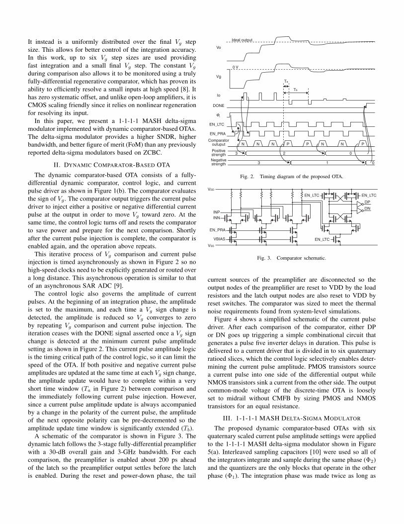
It instead is a uniformly distributed over the final Vg stepsize. This allows for better control of the integration accuracy.In this work, up to six Vg step sizes are used providingfast integration and a small final Vg step. The constant Vg
during comparison also allows it to be monitored using a trulyfully-differential regenerative comparator, which has proven itsability to efficiently resolve a small inputs at high speed [8]. Ithas zero systematic offset, and unlike open-loop amplifiers, it isCMOS scaling friendly since it relies on nonlinear regenerationfor resolving its input.
In this paper, we present a 1-1-1-1 MASH delta-sigmamodulator implemented with dynamic comparator-based OTAs.The delta-sigma modulator provides a higher SNDR, higherbandwidth, and better figure of merit (FoM) than any previouslyreported delta-sigma modulators based on ZCBC.
II. DYNAMIC COMPARATOR-BASED OTA
The dynamic comparator-based OTA consists of a fully-differential dynamic comparator, control logic, and currentpulse driver as shown in Figure 1(b). The comparator evaluatesthe sign of Vg . The comparator output triggers the current pulsedriver to inject either a positive or negative differential currentpulse at the output in order to move Vg toward zero. At thesame time, the control logic turns off and resets the comparatorto save power and prepare for the next comparison. Shortlyafter the current pulse injection is complete, the comparator isenabled again, and the operation above repeats.
This iterative process of Vg comparison and current pulseinjection is timed asynchronously as shown in Figure 2 so nohigh-speed clocks need to be explicitly generated or routed overa long distance. This asynchronous operation is similar to thatof an asynchronous SAR ADC [9].
The control logic also governs the amplitude of currentpulses. At the beginning of an integration phase, the amplitudeis set to the maximum, and each time a Vg sign change isdetected, the amplitude is reduced so Vg converges to zeroby repeating Vg comparison and current pulse injection. Theiteration ceases with the DONE signal asserted once a Vg signchange is detected at the minimum current pulse amplitudesetting as shown in Figure 2. This current pulse amplitude logicis the timing critical path of the control logic, so it can limit thespeed of the OTA. If both positive and negative current pulseamplitudes are updated at the same time at each Vg sign change,the amplitude update would have to complete within a veryshort time window (Ta in Figure 2) between comparison andthe immediately following current pulse injection. However,since a current pulse amplitude update is always accompaniedby a change in the polarity of the current pulse, the amplitudeof the next opposite polarity can be pre-decremented so theamplitude update time window is significantly extended (Tb).
A schematic of the comparator is shown in Figure 3. Thedynamic latch follows the 3-stage fully-differential preamplifierwith a 30-dB overall gain and 3-GHz bandwidth. For eachcomparison, the preamplifier is enabled about 200 ps aheadof the latch so the preamplifier output settles before the latchis enabled. During the reset and power-down phase, the tail
Vg
Vo
0 V
Io
Ideal output
N N PN P N N P
EN_LTC
Comparatoroutuput
3 1 0
3 2 0PositivestrengthNegativestrength
EN_PRA
DONE
i
Ta
Tb
Fig. 2. Timing diagram of the proposed OTA.
EN_LTC EN_LTC
EN_LTC
DP
DNINPINN
EN_PRA
VSS
VDD
VBIAS
Fig. 3. Comparator schematic.
current sources of the preamplifier are disconnected so theoutput nodes of the preamplifier are reset to VDD by the loadresistors and the latch output nodes are also reset to VDD byreset switches. The comparator was sized to meet the thermalnoise requirements found from system-level simulations.
Figure 4 shows a simplified schematic of the current pulsedriver. After each comparison of the comparator, either DPor DN goes up triggering a simple combinational circuit thatgenerates a pulse five inverter delays in duration. This pulse isdelivered to a current driver that is divided in to six quaternaryratioed slices, which the control logic selectively enables deter-mining the current pulse amplitude. PMOS transistors sourcea current pulse into one side of the differential output whileNMOS transistors sink a current from the other side. The outputcommon-mode voltage of the discrete-time OTA is looselyset to midrail without CMFB by sizing PMOS and NMOStransistors for an equal resistance.
III. 1-1-1-1 MASH DELTA-SIGMA MODULATOR
The proposed dynamic comparator-based OTAs with sixquaternary scaled current pulse amplitude settings were appliedto the 1-1-1-1 MASH delta-sigma modulator shown in Figure5(a). Interleaved sampling capacitors [10] were used so all ofthe integrators integrate and sample during the same phase (Φ2)and the quantizers are the only blocks that operate in the otherphase (Φ1). The integration phase was made twice as long as

OUTP OUTN
Dec
oder
DP DN
Pos
stre
ngth
Neg
stre
ngth
Fromcomparator
Fromcontrol logic
VDD
VSS
differ
ent W
/LPul
se g
ener
ator
Fig. 4. Current pulse driver schematic
1-z-12z-1
1/2
1-z-12z-1
1/2 1/2 z-2
1-z-1
z-3 v(z)
4 levels
4 levels
1-z-12z-1
1/2 1/4 z-1
1-z-14 levels
1-z-12z-1
1/2 1/8
1-z-14 levels
Combination digital filter
u(z)
(a)
DWA&
Encoder
Cs
2X
2Y
2
1
4-levelSC DAC
VCMIVCMO
Cs
Cs
VCMI
Cs
Ci
Ci
0.5
4-levelSC summing ADC
3
2
To nextstage
Binaryoutput
3Analoginput
DONEk
To nextstage
2Y
2X
2Y
2X
2Y
DONEk-1
2Y
2X
2X
2Y
2Y
Fromprevious stage
Sample in 2Quantize in 1
2
VCMO
2X
2X
Dynamiccomparator-based
OTA
(b)
Fig. 5. Modulator block diagram (a) and schematic of one stage (b).
the other phase extending the integration phase by 33%, andthus increasing the maximum sampling frequency by the samefactor. Figure 5(b) shows a simplified single-ended schematic ofone stage of the modulator. Capacitors Cs and Ci are 1 pF and0.5 pF, respectively, in the first stage and they are 0.5 pF and0.25 pF for the rest of the stages. The DONE signal isolates thecapacitors after integration to prevent unwanted charge transferafter the integrator output has settled but before the end ofclock phase Φ2. The quantizer passively sums its two inputswith weighted SCs and then quantizes the sum.
SummingADC
DA
C
SummingADC
SummingADC
SummingADC
DA
C
DA
C
DA
C
Cs
Cs
Ci
Modulator 1
X: Comparator, Y:Control logic, Z: Current pulse driver
X
YZ
YZ
X
YZ
X
YZ
X
Cs
Cs
Modulator 2 Modulator 3 Modulator 4
Ci
Cs
Cs
Ci
Cs
Cs
Ci
0.78 mm
0.55
mm
Fig. 6. Die microphotograph.
TABLE ISUMMARY OF THE EXPERIMENTAL RESULTS.
This work [5] [6] [7]Conventional OTA No No No NoCMOS technology 65 nm 45 nm 0.18 µm 3 µm TFTSupply (V) 1.2 1.0 1.1 1.8 11.2Sampling rate (MHz) 40 30 50 2.56 0.4OSR 8 30 64 128Bandwidth (MHz) 2.5 1.875 0.833 0.02 0.00156Peak SNDR (dB) 70.4 67.5 47.7 65.3 65.6Dynamic range (dB) 71.3 67.7 54.3 71 69Power (mW) 3.73 1.88 0.63 0.42 63.3FoM (fJ/conv-step) 276 259 1907 6980 13.0×10⁶
IV. EXPERIMENTAL RESULTS
The prototype delta-sigma modulator was implemented in asilicon area of 0.43 mm2 in a 65-nm LP CMOS technologywith standard-Vt devices only. A die photo of the prototype isshown in Figure 6. The measured peak SNDR is 70.4 dB andpower dissipation is 3.73 mW at VDD=1.2 V, fs=40 MHz, andOSR=8 without any calibration. Figure 7 shows the measuredoutput spectrum at the peak SNDR and SNDR versus the inputlevel. Figure 8 shows the measured output spectrum with a two-tone input near the edge of the signal bandwidth (2.5 MHz).The peak SNDR and IMD in this case are 67.3 dB and -89.5dBc, respectively. This 3-dB penalty in SNDR compared tothe single-tone measurement is inherent to the nature of thetwo-tone test in which the total power of the input is half (-3dB) of that of the single tone test for the same input swing.Table I summarizes the experimental results and compares theresults with other reported implementations of ZCBC-baseddelta-sigma modulators.
The FoM of 276 fJ/conv-step is not the best when comparedwith continuous-time delta-sigma modulators with a similarbandwidth and resolution. However, the modulator in this workprovides both fs (or bandwidth) scalability and power scala-bility over fs without requiring any circuit reconfiguration be-cause of the discrete-time delta-sigma modulation and dynamicoperation of the OTAs. The fs scalability requires RC timeconstant tuning in continuous-time delta-sigma modulators,

100 1k 10k 100k 1M 10M
−140
−120
−100
−80
−60
−40
−20
0P
SD
(dB
FS
/NB
W)
Frequency (Hz)
HD3-90.5 dBFS
-0.5 dBFS@50 kHz
VDD = 1.2 Vfs = 40 MHzOSR = 8SNDR = 70.4 dB
524288-pt DFTBlackman-Harris windowNBW = 152.6 Hz
2.5 MHz
(a)
−80 −70 −60 −50 −40 −30 −20 −10 0−10
0
10
20
30
40
50
60
70
Input level (dBFS)
SN
DR
(dB
)
VDD = 1.0 V, fs = 30 MHz, OSR = 8, fi = 50 kHz
VDD = 1.2 V, fs = 40 MHz, OSR = 8, fi = 50 kHz
(b)
Fig. 7. Measured modulator output spectrum (a) and SNDR versus input level(b).
Fig. 8. Measured modulator output spectrum with a two-tone input.
and power scalability over fs requires bias current adjustmentin both conventional discrete-time and continuous-time delta-sigma modulators. Both are difficult to achieve over a decaderange of fs as is shown here. The SNDR, SFDR, SNR, andpower consumption measured over fs are shown in Figure 9.The offset in the power consumption plot is the static powerdissipation of the master and local bias generation circuits,which could be reduced with a redesign.
V. CONCLUSION
A successful implementation of a 1-1-1-1 MASH delta-sigma modulator with dynamic-comparator based OTAs as
(a)
(b)
Fig. 9. Measured SNDR, SNR, and SFDR (a) and power consumption (b)over fs
replacements for conventional OTAs in a 65-nm LP CMOStechnology is presented. It efficiently performs SC integrationby iteration of asynchronously timed dynamic regenerative Vg
comparison and current pulse injection under digital amplitudecontrol. The prototype achieves a peak SNDR of 70.4 dB over a2.5-MHz bandwidth dissipating 3.73 mW from a 1.2-V supply.
REFERENCES
[1] L. Brooks and H.-S. Lee, “A Zero-Crossing-Based 8-bit 200 MS/sPipelined ADC,” Solid-State Circuits, IEEE Journal of, vol. 42, no. 12,pp. 2677–2687, Dec. 2007.
[2] J. Fiorenza, T. Sepke, P. Holloway, C. Sodini, and H.-S. Lee,“Comparator-Based Switched-Capacitor Circuits for Scaled CMOS Tech-nologies,” IEEE Journal of Solid-State Circuits, vol. 41, no. 12, pp. 2658–2668, Dec. 2006.
[3] L. Brooks and H.-S. Lee, “A 12b, 50 MS/s, Fully Differential Zero-Crossing Based Pipelined ADC,” IEEE Journal of Solid-State Circuits,vol. 44, no. 12, pp. 3329–3343, Dec. 2009.
[4] J. Chu, L. Brooks, and H.-S. Lee, “A zero-crossing based 12b 100MS/spipelined ADC with decision boundary gap estimation calibration,” inVLSI Circuits, 2010 IEEE Symposium on, Jun. 2010, pp. 237–238.
[5] T. Musah, S. Kwon, H. Lakdawala, K. Soumyanath, and U.-K. Moon, “A630 µW zero-crossing-based ΔΣ ADC using switched-resistor currentsources in 45nm CMOS,” in IEEE Custom Integrated Circuits Confer-ence, Sep. 2009, pp. 1–4.
[6] M.-C. Huang and S. luan Liu, “A Fully Differential Comparator-BasedSwitched-Capacitor ΔΣ Modulator,” IEEE Transactions on Circuits andSystems II, vol. 56, no. 5, pp. 369–373, May. 2009.
[7] W.-M. Lin, C.-F. Lin, and S.-I. Liu, “A CBSC second-order sigma-delta modulator in 3 µm LTPS-TFT technology,” in Solid-State CircuitsConference, 2009. A-SSCC 2009. IEEE Asian, Nov. 2009, pp. 133–136.
[8] P. Nuzzo, F. De Bernardinis, P. Terreni, and G. Van der Plas, “NoiseAnalysis of Regenerative Comparators for Reconfigurable ADC Archi-tectures,” Circuits and Systems I: Regular Papers, IEEE Transactions on,vol. 55, no. 6, pp. 1441–1454, Jul. 2008.
[9] S.-W. Chen and R. Brodersen, “A 6-bit 600-MS/s 5.3-mW AsynchronousADC in 0.13-µm CMOS,” Solid-State Circuits, IEEE Journal of, vol. 41,no. 12, pp. 2669–2680, Dec. 2006.
[10] A. Gharbiya and D. Johns, “On the implementation of input-feedforwarddelta-sigma modulators,” IEEE Transactions on Circuits and Systems II,vol. 53, no. 6, pp. 453–457, Jun. 2006.