Embed Size (px)
Citation preview
Temporal partitioning methodology optimizing FPGA resources
for dynamically reconfigurable embedded real-time system
C. Tanougast*, Y. Berviller, P. Brunet, S. Weber, H. Rabah
Laboratoire d’Instrumentation Electronique de Nancy, Universite de Nancy 1, BP 239, Vandoeuvre Les Nancy 54506, France
Received 2 September 2002; revised 22 November 2002; accepted 27 November 2002
Abstract
In this paper we present a new temporal partitioning methodology used for the data-path part of an algorithm for the reconfigurable
embedded system design. This temporal partitioning uses an assessing trade-offs in time constraint, design size and field programmable gate
arrays device parameters (circuit speed, reconfiguration time). The originality of our method is that we use the dynamic reconfiguration in
order to minimize the number of cells needed to implement the data-path of an application under a time constraint. Our method consists, by
taking into account the used technology, in evaluating the algorithm area and operators execution time from data flow graph. Thus, we
deduce the right number of reconfigurations and the algorithm partitioning for Run-Time Reconfiguration implementation. This method
allows avoiding an oversizing of implementation resources needed. This optimizing approach can be useful for the design of an embedded
device or system. Our approach is illustrated by various reconfigurable implementations of real time image processing data-path.
q 2003 Elsevier Science B.V. All rights reserved.
Keywords: Field programmable gate arrays; Embedded system; Temporal partitioning; Run-time reconfiguration; Dynamically reconfigurable systems; Image
processing; Design implementation; High-level synthesis
1. Introduction
Since the introduction of field programmable gate arrays
(FPGA), the process of digital systems design has changed
radically [1,2]. Indeed, FPGAs occupy an increasingly
significant place in the realization of real time applications
and has allowed the appearance of a new paradigm:
hardware as flexible as programming.
The dynamically reconfigurable computing consists in
the successive execution of a sequence of algorithms on the
same device. The objective is to swap different algorithms
on the same hardware structure, by reconfiguring the FPGA
array in hardware several times in a constrained time and
with a defined partitioning and scheduling [3,4]. Dynamic
reconfiguration offers important benefits for the implemen-
tation of designs. Several architectures have been designed
and have validated the dynamically reconfigurable comput-
ing concept for the real time processing [5–9]. However,
the optimal decomposition (partitioning) of an algorithm by
exploiting the run-time reconfiguration (RTR) is a domain
in which many works are left. The works in the domain of
temporal partitioning and logic synthesis exploiting the
dynamic reconfiguration generally focus on the application
development approach [10]. Thus, firstly we observe that
the efficiency obtained is not always optimum with respect
to the available spatio-temporal resources. Secondly, the
choice of the number of partitions is never specified.
Thirdly, this can be improved by a judicious temporal
partitioning [11].
We discuss here the partitioning problem for the RTR. In
the task of implementing an algorithm on reconfigurable
hardware, we can distinguish two approaches [10]. The
most common is what we call the application development
approach and the other is what we call the system design
approach. In the first case, we have to fit an algorithm with
an optional time constraint in an existing system made from
a host CPU connected to a reconfigurable logic array. In this
case, the goal of an optimal implementation is to minimize
one or more of the following criteria: processing time,
memory bandwidth, number of reconfigurations and power
consumption. In the second case, we have to implement an
0141-933/03/$ - see front matter q 2003 Elsevier Science B.V. All rights reserved.
PII: S0 14 1 -9 33 1 (0 2) 00 1 02 -3
Microprocessors and Microsystems 27 (2003) 115–130
www.elsevier.com/locate/micpro
* Corresponding author. Tel.: þ33-383-6841-59; fax: þ33-383-6841-53.
E-mail addresses: [email protected] (C. Tanougast),
[email protected] (Y. Berviller), [email protected] (P.
Brunet), [email protected] (S. Weber), [email protected] (H.
Rabah).
algorithm with a required time constraint on a system
throughout the design exploration phase. The design
parameter is the size of the logic array that is used to
implement the data-path part of the algorithm. Here an
optimal implementation is the one that leads to the minimal
area of the reconfigurable array.
Previous advanced works in the field of temporal
partitioning and synthesis for RTR architecture [12–19]
focus on application development approach targeting
already designed reconfigurable architecture. These meth-
odologies are used in the domain of existing reconfigurable
accelerators or reconfigurable processors. All these
approaches assume the existence of a resources constraint.
The most important thing here is that the number of
reconfigurable resources is a predefined constant
(implementation constraint). In this strategy, the associated
tools capture the algorithm and the characteristics of the
target platform on which the algorithm will be implemented.
In this case, the goal is to minimize the processing time and/
or the memory bandwidth requirement. Moreover, all these
approaches are not capable of solving practical DRL
(dynamically reconfigurable logic) synthesis problems yet.
These techniques use in general simplified models of
dynamically reconfigurable systems, which often ignore
the impact of routing or reconfiguration resource sharing in
order to reduce complexity of a DRL design space search.
Among them, there is the GARP project [12]. The goal
of GARP is the hardware acceleration of loops in a C
program by the use of the data path synthesis tool GAMA
[13] and the GARP reconfigurable processor. GARP is a
processor tightly coupled to a custom FPGA-like array
and designed specially to speed-up the execution of
general case loops. The logic array has a DMA feature
and is tailored to implement 32 bits wide arithmetic and
logic operations with the control logic, all this allows to
minimize the reconfiguration overhead. GAMA is a fast
mapping and placement tool for the data-path implemen-
tation in FPGAs. It is based on a library of patterns for all
possible data-path operators. The SPARCS project [14,15]
is a CAD tool suite tailored for applications development
on multi-FPGAs reconfigurable computing architectures.
Such architectures need both spatial and temporal
partitioning, a genetic algorithm is used to solve the
spatial partitioning problem. The main cost function used
here is the data memory bandwidth. Other works propose
a strategy to automate the design process that considers all
possible optimizations (partitioning and task scheduling)
that can be carried out from a particular reconfigurable
system [16,17]. Shirazi et al. and Luk et al. [18,19]
proposes both a model and a methodology to take
advantages of common operators in successive partitions.
A simple model for specifying, visualizing and developing
designs that contains reconfigurable elements in run-time
has been proposed. This judicious approach allows
reducing the configuration time and thus the application
execution time. But additional logic resources (area) are
required to realize an implementation with this approach.
Furthermore this model does not include timing aspects in
order to satisfy the real time and it does not specify the
partitioning of the implementation. Indeed, the algorithm
partitioning must be previously known to determine the
elements that do not need to be reconfigured for the next
step. However, this concept is interesting to use for DRL
designs simulation as Dynamic circuit switching (DCS)
[20]. This simulation uses virtual multiplexors, demulti-
plexors and switches, which are implemented to simulate
the dynamic configuration design.
These interesting works do not pursue the same goal
as we do. In priority, we try to find the minimal area that
allows meeting the time-constraint. This is different from
searching the minimal memory bandwidth or execution
time which allows meeting the resources constraint.
Here, we propose a temporal partitioning that uses
dynamic reconfiguration of FPGA (also called DRL
Scheduling) to minimize the implementation logic area.
Each partition corresponds to a temporal floorplanning
for DRL embedded systems (Fig. 1) [21]. We search the
minimal floorplan area that implements successively a
particular algorithm. This approach improves the per-
formance and efficiency of the design implementation. In
contrast to previous work, our aim is to obtain, from an
algorithm description, a target technology and implemen-
tation constraints, the characteristics of the platform to
design or to use. This allows avoiding an oversizing of
implementation resources. For example, by summarizing
the sparse information found in some articles [22–24],
we can assume the following. Suppose we have to
implement a design requiring P equivalent gates and
taking an area SFC of silicon in the case of a full custom
ASIC design. Then we will need about 10 £ SFC in the
case of a standard cell ASIC approach and about 100 £
SFC if we decide to use an FPGA. But the large
advantage of the FPGA is, of course, its great flexibility
and the speed of the associated design flow. This is
probably the main reason to include a FPGA array on
System on Chip platforms. Suppose that a design is
requiring that 10% of the gates must be implemented as
full custom, 80% as standard cell ASIC and 10% in
FPGA cells. By roughly estimating the areas, we come to
the following results: The FPGA array will require more
than 55% of the die area, the standard cell part more
than 44% and the full custom part less than 1%. In such
a case it could make sense to try to reduce the equivalent
gate count needed to implement the FPGA part of the
application. This is interesting because the regularity of
the FPGA part of the mask leads to a quite easy
modularity of the platform with respect to this parameter.
Embedded systems design can take several advantages
of the use our approach based on RTR FPGAs. The most
obvious is the possibility to frequently update the digital
hardware functions. But we can also use the dynamic
resources allocation feature to instantiate each operator
C. Tanougast et al. / Microprocessors and Microsystems 27 (2003) 115–130116
only for the minimal required time. This permits to
enhance the silicon efficiency by reducing the reconfigur-
able array’s area [25,26]. Our goal is the definition of a
RTR methodology, included in the architectural design
flow, which allows minimizing the FPGA resources
needed for the implementation of a time constrained
algorithm. So, the challenge is double. Firstly to find
trade-offs between flexibility and algorithm implemen-
tation efficiency through the programmable logic-array.
Secondly to obtain computer-aided design techniques for
optimal synthesis which include the dynamic reconfigura-
tion in an implementation.
The rest of this paper is organized as follows. Section 2
provides a formal definition of our partitioning problem. In
Section 3 we present the partitioning strategy. In Section 4
we illustrate the application of our method with two image-
processing algorithms. In the first example, we carry out the
method in an automatic way such as we will describe it. In
the second example, we apply our method while showing
the possibility of further evolution. The aim is to make
possible improvements of the suggested method. In Sections
5 and 6 we discuss the approach compared to architectural
synthesis, conclude and present future works.
2. Problem formulation
Currently the partitioning for RTR is often made at
boundaries of algorithm operators. This means that, for
example the partitioning of the image processing algorithm
is made at image operators like filters, edge detection
operators, and so on. In contrast with this decomposition, we
work on the global algorithm independently of image
operators. Our method is based on elementary arithmetic
and logic operators of the algorithm (adders, subtractor,
multiplexers, registers etc.) of the algorithm. The analysis of
the operators leads to a register transfer level (RTL)
decomposition of the DFG. This partitioning is then
independent of high-level operators (macro-operators).
The RTR partitioning for the real time application could
be classified as a spatio-temporal problem. That is as a time
constrained problem with dynamic resource allocations in
contrast with the scheduling for RTR [27]. Then, we make
the following formulations about the application. Firstly, the
algorithm can be modeled as an acyclic data flow graph
(DFG) denoted here by GðV ;EÞ where the set of vertices
V ¼ {O1;O2;…;Om} corresponds to the arithmetic and
logical operators and the set of directed edges E ¼
{e1; e2;…ep} represents the data dependencies between
operations. Secondly, The application has a critical time-
constraint T. The problem to solve is the following:
For a given FPGA family we have to find the set
{P1;P2;…Pn} of sub graphs of G such as:
[n
i¼1
Pi ¼ G; ð1Þ
and that allows to execute the algorithm by meeting the
time-constraint T and the data dependencies modeled by E
and requires the minimal amount of FPGA cells. The
number of FPGA cells used, which is an approximation of
the area of the array, is given by Eq. (2), where Pi is one
among the n partitions.
maxi[{1…n}
ðAreaðPiÞÞ: ð2Þ
The FPGA resources needed by a partition i is given by
Eq. (3), where Mi is the number of elementary operators in
partition Pi and AreaðOkÞ is the amount of resources needed
Fig. 1. Temporal partitioning with a minimized floorplan area.
C. Tanougast et al. / Microprocessors and Microsystems 27 (2003) 115–130 117
by operator Ok:
AreaðPiÞ ¼X
k[{1…Mi}
AreaðOkÞ: ð3Þ
3. Temporal partitioning
A typical search sequence of temporal partitions includes
the following steps:
1. Definition of the constraints, the type of the design (use
dynamic configurable platform fixed-resources or recon-
figurable embedded design): time constraint, data-block
size, bandwidth bottleneck, memory size, consumption)
and the target technology.
2. DFG capture using design entry.
3. Determination of temporal partitioning.
4. Generation of the configuration bitstream of each
temporal floorplan for the final design.
Here, we are only interested in dynamically configurable
embedded design. In our case, the temporal partitioning
methodology in the design flow is depicted in Fig. 2. Our
method, which determines the minimal floorplan area, is
structured on three parts. In the first, from technology target
library and constraint parameters, we compute an approxi-
mation of the number of partitions, and then we deduce
boundaries of each temporal floorplans. Finally we refine
when it is possible the final partitioning. Constraint
parameters are used to adjust temporal partitioning solution
until all design constraints are met. This method can be seen
as a heuristic approach.
3.1. Number of partitions
In order to reduce the search domain we first estimate the
minimum number of partitions that we can make and the
resources by partition. To do this, we use an operator library
that is target dependent. This library allows association of
two attributes to each vertex of the graph G. These attributes
are ti and AreaðOiÞ; respectively, the maximal path delay
and the number of elementary FPGA cells needed for
operator Oi: The symbol i represents the index of a
particular operator in the DFG. These two quantities are
functions of the size (number of bits) of the data to process.
If we know the size of the initial data to process, it is easy to
deduce the size at each node by a ‘software execution’ of the
graph with the maximal value for the input data.
Furthermore, we make the following assumptions:
The data to process are grouped in blocks of N data.
The number of operations to apply to each data in a block
is deterministic (i.e. not data dependent).
There are pipeline registers between all nodes of the graph.
The reconfiguration time of the FPGA technology used
can be approximated by a linear function of the area of the
functional units being downloaded. Which is realistic in
practice. The configuration speed is a constant and a
characteristic of the FPGA (see Section 4).
Thus, the minimal operating time period tomax is given
by:
tomax ¼ maxi[{1…m}
ðtiÞ ð4Þ
Where {1…m} is the set of all operators of data-path G and
ti is execution time of operator Oi: The total number C of
Fig. 2. General outline of the temporal partitioning in the design flow.
C. Tanougast et al. / Microprocessors and Microsystems 27 (2003) 115–130118
cells used by the application is given by:
C ¼X
i[{1…m}
AreaðOiÞ ð5Þ
The main constraint is the need for real time processing. We
suppose that the algorithms are partitioned in n steps
corresponding to n execution–reconfiguration pairs. For a
given FPGA family characterized by a reconfiguration speed
V, the working frequency of each step must verify the
following inequality:
Xn
i¼1
si þ N·Xn
i¼1
tei # T 21
V·Xn
i¼1
AreaðPiÞ ð6Þ
Where AreaðPiÞ is the number of FPGA’s logic cells needed
by Pi; N is the number of data to process, n the number of
reconfigurations ðn [ INÞ; T is the upper limit of processing
time (time constraint), si corresponds to the prologue and
epilogue of pipeline in the partition Pi and tei is the
elementary processing time of a data in the ith step. In one
partition, the elementary processing time corresponds to the
longest execution time among all operators present in the
partition Pi: So, we have:
tei ¼ maxk[{1…Mi}
ðtkÞ ð7Þ
Using Eqs. (4)–(6), we obtain the minimum number
of partitions n as given by Eq. (8) and the corresponding
optimal size Cn (number of cells) of each partition by Eq. (9).
n ¼ RoundT
ðN þ sÞ·tomax þC
V
0BB@
1CCA ð8Þ
Where V is the configuration speed expressed by cells/s, C the
number of cells required to implement the entire DFG, N the
number of data in a block, s the total latency cycles of all
data-path and tomax the propagation delay of the slowest
operator in the DFG. This time is fixed by the maximum time
between two successive vertices of graph G thanks to the
fully pipelined process.
Cn ¼C
nð9Þ
The first expression of the denominator in Eq. (8) is the
effective processing time of one data block and the second
expression is the consumed time to load the n configurations
(total reconfiguration time of G).
In most application domain like image processing (see
Section 4), we can neglect the impact of the latency time in
comparison with the processing time (N q number of
pipeline stages (s)). So, we can approximate Eq. (8) by Eq.
(10).
n < RoundT
N·tomax þC
V
0BB@
1CCA ð10Þ
A limit in the use of dynamic reconfiguration of FPGA
has been exhibited [28], because the impact of
reconfiguration time depends on the size of the data
block to treat. Two conditions must be satisfied to
allow dynamic configuration. First, the sample fre-
quency of data must be less than the maximum
hardware computation frequency. Secondly, the data
must be computed in blocks with a significant size to
reduce the reconfiguration overhead. In this case,
silicon reduction can be achieved, but the major
advantage of dynamic reconfiguration is the possibility
of changing the algorithms (which can be data
dependent) in real time and to optimize implementation
area of designs.
From the analysis of the value of n, we can extract some
information on the parameters characterizing of the system
needed to realize the implementation. We describe these
different cases below:
1) n . 1: That means it is possible to realize a RTR
partitioning. In this case, an optimization is possible and
allows obtaining a reduction of the logic area of implemen-
tation with the technology used. n corresponds to the number
of partitions that we are sure to obtain.
2) n # 1: In this case, with the RTR partitioning it is not
possible to ensure the time constraint. Here, only static
implementation with or without parallel processing allows
respecting the time constraint.
If n ¼ 1: This case means that only static implementation
is sufficient to meet the constraints with the used
technology.
If n , 1: This means that to ensure the constraint it is
necessary to realize a static implementation with a proces-
sing parallelism. 1/n gives the degree of processing
parallelism. In practice 1/n [ IN. In this case, it is necessary
to know if the target technology is interesting for the
implementation of the application.
The pseudo algorithm of the determination of n and Cn is
given below. We annotate the DFG by using the operator
library. We cover all the nodes in the DFG, we accumulate
the area and we search the maximal execution time among
the operators of the DFG.
V, N, T ( constants//Capture constant parameters of/of
target and constraints
G ( DFG//DFG capture of the application
C ( 0//Total area variable,
TO ( 0//Maximal operator time variable
for each node Ni in G
TO ( max (TO, Ni.ti)//return current max
//of execution time
C ( C þ Ni.Area//add area of current/node
end for
n ( T/[(N TO) þ rt( )]//compute n and Cn
Cn ( C/n
C. Tanougast et al. / Microprocessors and Microsystems 27 (2003) 115–130 119
3.2. Initial partitioning
A pseudo algorithm of the partitioning scheme is given
below.
G ( data flow graph of the application
P1;P2;…;Pn ( empty partitions
for i in {1…n}
C ( 0
while C , Cn
append (Pi; First_Leave(G))
C ( C þ First_Leave(G).Area
remove (G, First_Leave(G))
end while
end for
We cover again the graph from the leaves to the root(s)
by accumulating the sizes of the covered nodes until the sum
is as close as possible to Cn: These covered vertices make
the first partition. We remove the corresponding nodes from
the graph (command ‘remove (G, First_Leave(G))’). The
goal of this function is to avoid considering twice the same
node and to ensure the data dependencies. Then, we iterate
the covering until the remaining graph is empty. The
partitioning is then finished.
There is a great degree of freedom in the implementation
of the First_Leave( ) function, because there are usually
many leaves in a DFG. The only strong constraint is that the
choice must be made in order to guarantee the data
dependencies across the whole partition.
The choice of a node among the leaves of the DFG can be
carried out in several ways. Since the leaves are terminal
nodes, they meet the data dependency constraints. So, the
reading of the leaves of the DFG can be random or ordered
for example. In our case it is ordered. We consider as a two-
dimensional table containing parameters relating to the
operators of the DFG. First_Leave( ) is carried out in the
reading order of the table containing the operator arguments
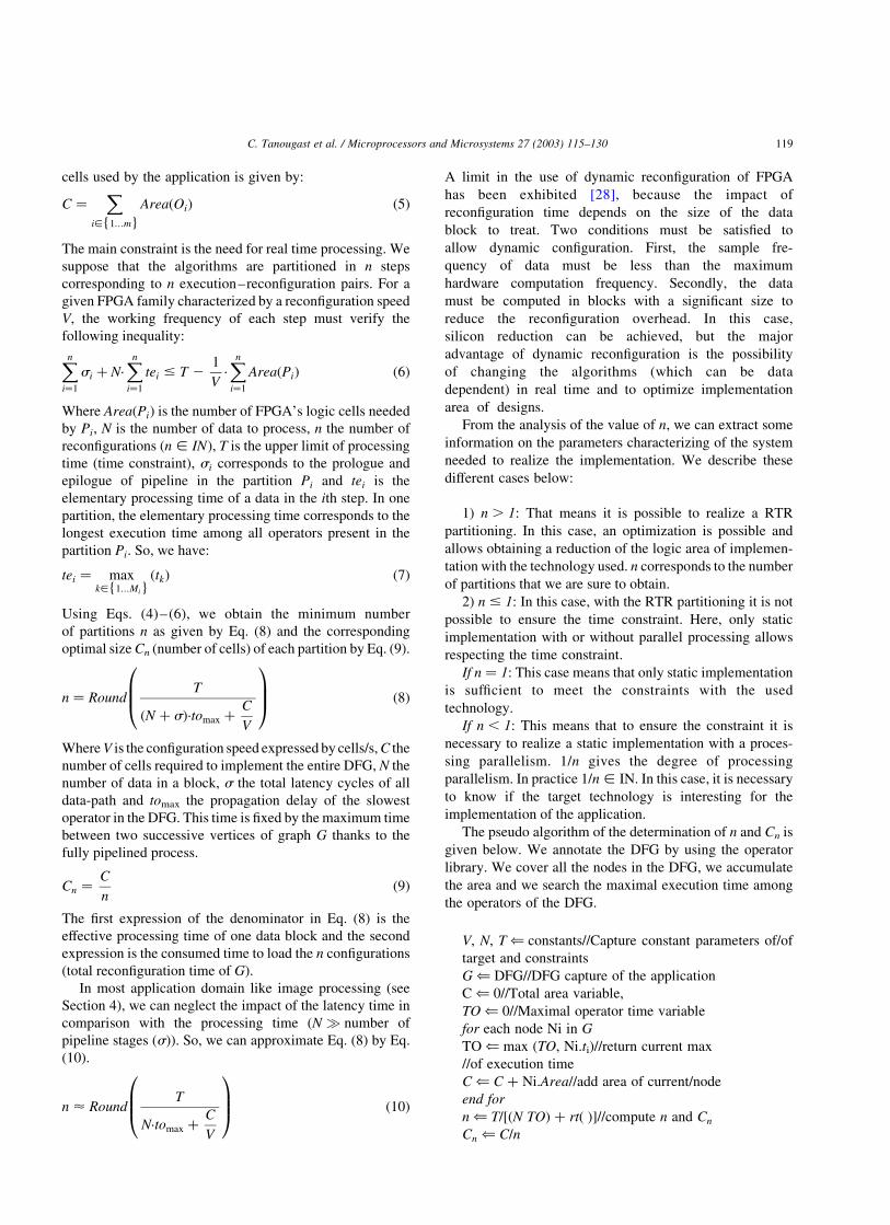
of the DFG (left to right) (Fig. 3). In our case, the pseudo
algorithm of First_Leave( ) function is given below.
M[ ][ ] ( G; DFG capture
for M[i ][ j ] in M
if M[i ][ j ] – 0
first_leave(G).area ( M[i ][ j ].area;
first_leave(G).tk ( M[i ][ j ].tk;
end if
end for
3.3. Refinement after implementation
After placement and routing of each partition that was
obtained in the initial phase we are able to compute the
exact processing time. It is also possible to take into account
the value of the synthesized frequency close to the maximal
processing frequency for each partition.
The analysis of the gap between the total processing time
(configuration and execution) and the time constraint permits
to make a decision about the partitioning. If it is necessary to
reduce the number of partitions or possible to increase it, we
return to the step described in Section 3.2 with a new value for
n. Else the partitioning is considered as a final one (see Fig. 2).
In this case, if time remains after the execution of all
partitions, but it is not enough to add one, we decrease this
time by reducing the working frequency in one or more
partitions. Thus, we limit the consumption of the application.
This heuristic partitioning is the best that we can obtain
with this straightforward method. However, we do not have
enough criteria to compare our heuristic approach to the
existing methods based for example on mathematical
resolution. For this reason we cannot conclude that our
method always leads to an optimal solution.
4. Applications to image processing
In this section, we illustrate and model parameters to
apply our method in the field of the images processing. This
application area is a good choice for our approach because
the processing are generally characterized by regular
operators (data-path) and the data are naturally organized
in blocks (the images). Large blocks of data to process leads
to a reduced overhead of reconfiguration time. Otherwise,
the time dedicated to a processing is mainly allocated for
reconfigurations. Moreover, there are many low level
processing algorithms that can be modeled by a data flow
graph and the time constraint is usually the image
acquisition period. We assume that the images are taken
at a rate of 25 per second with a spatial resolution of
512 £ 512 pixels and each pixel gray level is an eight bits
value. Then, we have a time constraint of 40 ms by image to
assure the real time processing.
4.1. Algorithms
We illustrate our method with two image processing
algorithms. The first algorithm used here is a 3 £ 3 median
Fig. 3. Labeling and reading of the DFG.
C. Tanougast et al. / Microprocessors and Microsystems 27 (2003) 115–130120
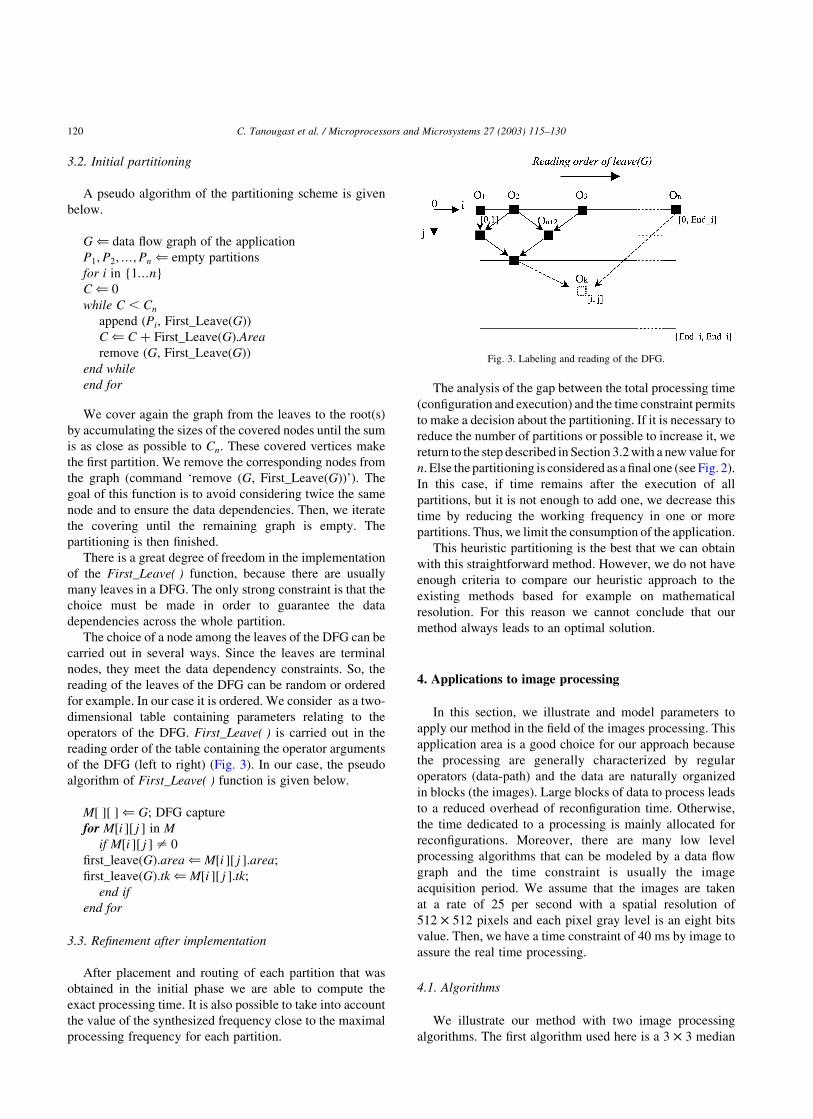
filter followed by an edge detector and its general view is
given on Fig. 4.
In this example, we consider a separable median filter
[29] and a Sobel operator. The median filter provides the
median value of three vertical successive horizontal median
values. Each horizontal median value is simply the median
value of three successive pixels in a line. This filter allows to
eliminate the impulsion noise while preserving the edges
quality. The principle of the implementation is to sort the
pixels in the 3 by 3 neighborhood by their gray level value
and then to use only the median value (the one in 5th
position over 9). This operator is constituted of eight bits
comparators and multiplexers. A Sobel operator achieves
the gradient computation. This corresponds to a convolution
of the image by successive application of two mono-
dimensional filters. These filters are the vertical and
horizontal Sobel operator, respectively. The final gradient
value of the central pixel is the maximum absolute value
from vertical and horizontal gradient. The line delays are
made with components external to the FPGA (Fig. 4).
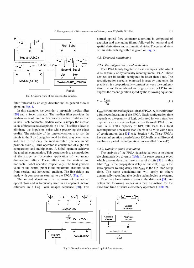
The second algorithm is an estimator of the normal
optical flow and is frequently used in an apparent motion
estimator in a Log–Polar images sequence [30]. This
normal optical flow estimator algorithm is composed of
gaussian and averaging filters, followed by temporal and
spatial derivatives and arithmetic divider. The general view
of this data-path algorithm is given on Fig. 5.
4.2. Temporal partitioning
4.2.1. Reconfiguration speed evaluation
The FPGA family targeted in these examples is the Atmel
AT40k family of dynamically reconfigurable FPGA. These
devices can be totally configured in lesser than 1 ms. The
reconfiguration speed is expressed in area by time units. In
practice it is a proportionality constant between the configur-
ation time and the number of used logic cells in the FPGA. We
express the reconfiguration speed by the following equation:
V ¼Cmax
TG
ð11Þ
Cmax is thenumberof logiccells in theFPGA.TG is the timefor
a full reconfiguration of the FPGA. Each configuration time
depends on the quantity of logic cells used for each step. We
express thearea in termsof logiccellsof theusedFPGA.Inour
case, AT40K20’s capacity of 819 Cells leads to a total
reconfiguration time lower than 0.6 ms at 33 MHz with 8 bits
of configuration data [31] (see Section 4.3). These FPGAs
have aconfiguration speed of about 1365 cells per millisecond
and have a partial reconfiguration mode (called ‘mode 4’).
4.2.2. Dataflow graph annotation
The analysis of the FPGA datasheet allows us to obtain
the characteristics given in Table 1 for some operator types
which process data that have a size of D bits [31]. In this
table Tcell is the propagation delay of one cell; Trout is the
intra operator routing delay and Tsetup is the flip–flop setup
time. The same considerations will apply to others
dynamically reconfigurable device technologies or systems.
From the characteristics given in the datasheet [31], we
obtain the following values as a first estimation for the
execution time of usual elementary operators (Table 2).
Fig. 4. General view of the images edge detector.
Fig. 5. General view of the normal optical flow estimator.
C. Tanougast et al. / Microprocessors and Microsystems 27 (2003) 115–130 121
In practice, there is a linear relationship between the
estimated individual execution time and the real execution
time. Indeed, when a operator is included in daisy chain of
operator there is a routing time needed between two
successive nodes. Fig. 6 shows a plot of the estimated
individual execution time versus the real execution time for
some different usual low-level operators. Those operators
have been implemented individually in the FPGA array
between registers. Then, we have measured and rounded at
the nearest integer the obtained real execution times (Fig. 6).
From this observation, the estimated individual
execution time allows obtaining an approximation of
the real execution times of the operators contained in the
data-path. With the FPGA technology used, this coeffi-
cient has a value of about 1.5 (see Fig. 6). The results
are more exact as the algorithm is regular such as the
data-path (simple cascade of the operators). The evalu-
ation of the routing in the general case is a more difficult
task. The execution time after implementation of a
regular graph does not depend on the type of operator. A
weighting coefficient binds the real execution time with
the estimated one. This coefficient approximates the
routing delay between operators based on the estimated
execution time. So, these routing delays are a constant
portion of the duration of each step. This is realistic and
easy to exploit analytically.
With these estimations and by taking into account the
increase of data size caused by processing, we can annotate
the dataflow graph. Then, we can deduce the number and the
characteristics of all the operators. Table 3 gives these data
for the first algorithm example. In this table, the execution
time is an estimation of the real execution time.
From these data, we deduce the number of partitions
needed to implement a dedicated data-path in an optimized
way. Thus, for the edges detector, among all operators of the
data-path we can see that the slowest operator is an eight-bit
comparator and that we have to reconfigure 467 cells. Using
Eq. (10), we obtain a value of three for n. The size of each
partition (Cn) should be about 156 cells. Table 4 summarizes
the estimation for a RTR implementation of the algorithm.
For the data-path part of the second algorithm (normal
optical flow), we can estimate again the logic resources
required for the implementation (see Table 5). Thus, among
all operators of the data-path, we can see that the slowest
operator is a fifteen bit subtractor and that we have to
reconfigure 863 cells. Using Eq. (10), we obtain a value
superior to three for n. Here, it is possible to implement this
global data-path with about 264 cells in each partition (Cn).
Table 6 summarizes the estimation for a RTR implemen-
tation of the algorithm.
In practice, the partitioning of the data-path must also
take into account the memory bandwidth bottleneck. That is
why, the best practical partitioning needs to keep the data
throughput in accordance with the performances of the used
memory.
4.2.3. Optimizing memory bandwidth
The first aim of our methodology is to create partitions
with area as homogeneous as possible. If this is the wish of a
designer, he must also avoid going over technology
constraints like memory bandwidth. To help the designer,
the tool provides the data size requirement for each level of
the DFG. By the way, we are able to see where the
partitioning might produce a failure or an optimal solution.
Moreover, in order to automate this refinement, the program
can defer or anticipate the partitioning of the DFG to make it
where the memory bandwidth requirement is minimal. The
search is restricted to a neighborhood of the theoretical
partitioning points. This neighborhood is adjustable to keep
the compromise between homogeneous areas and memory
Table 1
Usual operator characterization (AT40k)
D bits operator Number
of cells
Estimated
execution time
Multiplication
or division by 2k
0 0
Adder or subtractor D þ 1 D(Tcell þ Trout) þ Tsetup
Multiplexer D Tcell þ Tsetup
Comparator 2D (2D-1)(Tcell) þ 2Trout þ Tsetup
Absolute value
(two’s complement)
D 2 1 D(Tcell þ Trout) þ Tsetup
Additional synchronization
register
D Tcell þ Tsetup
Table 2
Estimated execution time of some eight bit operators in AT40k technology
Eight bits operators Estimated execution
time (ns)
Comparator 27.34
Multiplexer 5
Absolute value 22.07
Adder, Subtractor 16.46
Combinatory logic with
inter-propagation logic cell
17
Combinatory logic without
inter-propagation logic cell
5
Fig. 6. Estimated time versus real execution time of some operators in
AT40k technology.
C. Tanougast et al. / Microprocessors and Microsystems 27 (2003) 115–130122
bandwidth minimization (Fig. 7). The size of the memory
bandwidth (data size and real working frequency) along the
DFG is known between each operator lines. When we create
the DFG, edges receive a size argument that represents the
data size of the bus between two nodes (operators). So,
when we add all edges size arguments crossing nodes lines,
we obtain the total data size in use at this point of the DFG.
By applying the method described in Section 3, we
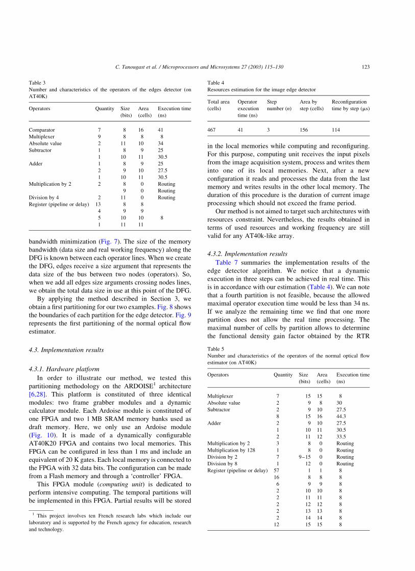
obtain a first partitioning for our two examples. Fig. 8 shows
the boundaries of each partition for the edge detector. Fig. 9
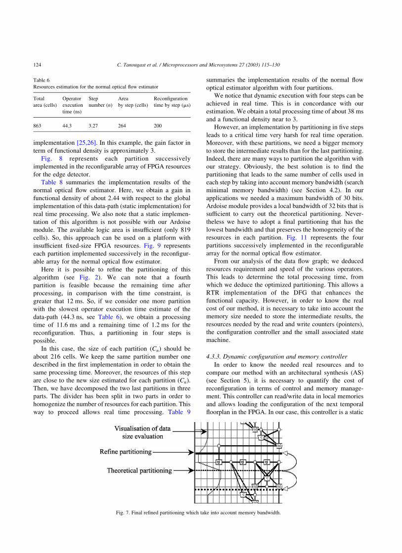
represents the first partitioning of the normal optical flow
estimator.
4.3. Implementation results
4.3.1. Hardware platform
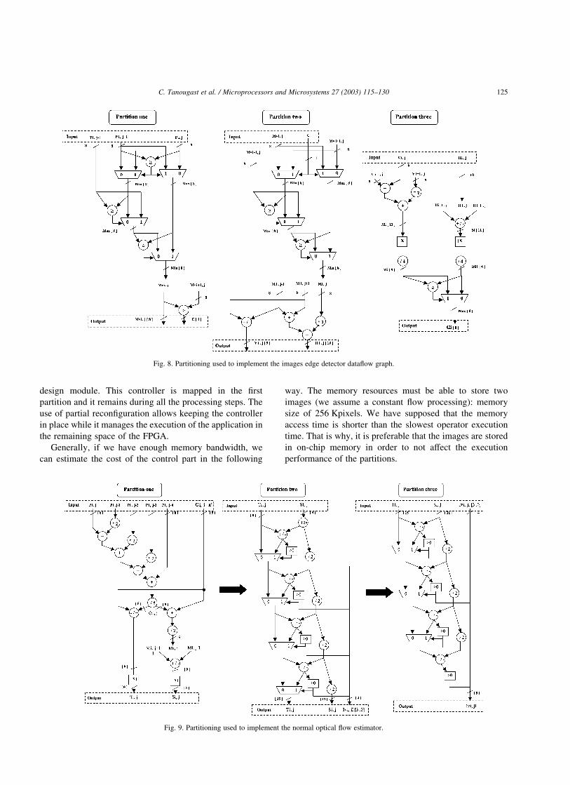
In order to illustrate our method, we tested this
partitioning methodology on the ARDOISE1 architecture
[6,28]. This platform is constituted of three identical
modules: two frame grabber modules and a dynamic
calculator module. Each Ardoise module is constituted of
one FPGA and two 1 MB SRAM memory banks used as
draft memory. Here, we only use an Ardoise module
(Fig. 10). It is made of a dynamically configurable
AT40K20 FPGA and contains two local memories. This
FPGA can be configured in less than 1 ms and include an
equivalent of 20 K gates. Each local memory is connected to
the FPGA with 32 data bits. The configuration can be made
from a Flash memory and through a ‘controller’ FPGA.
This FPGA module (computing unit) is dedicated to
perform intensive computing. The temporal partitions will
be implemented in this FPGA. Partial results will be stored
in the local memories while computing and reconfiguring.
For this purpose, computing unit receives the input pixels
from the image acquisition system, process and writes them
into one of its local memories. Next, after a new
configuration it reads and processes the data from the last
memory and writes results in the other local memory. The
duration of this procedure is the duration of current image
processing which should not exceed the frame period.
Our method is not aimed to target such architectures with
resources constraint. Nevertheless, the results obtained in
terms of used resources and working frequency are still
valid for any AT40k-like array.
4.3.2. Implementation results
Table 7 summaries the implementation results of the
edge detector algorithm. We notice that a dynamic
execution in three steps can be achieved in real time. This
is in accordance with our estimation (Table 4). We can note
that a fourth partition is not feasible, because the allowed
maximal operator execution time would be less than 34 ns.
If we analyze the remaining time we find that one more
partition does not allow the real time processing. The
maximal number of cells by partition allows to determine
the functional density gain factor obtained by the RTR
Table 3
Number and characteristics of the operators of the edges detector (on
AT40K)
Operators Quantity Size
(bits)
Area
(cells)
Execution time
(ns)
Comparator 7 8 16 41
Multiplexer 9 8 8 8
Absolute value 2 11 10 34
Subtractor 1 8 9 25
1 10 11 30.5
Adder 1 8 9 25
2 9 10 27.5
1 10 11 30.5
Multiplication by 2 2 8 0 Routing
9 0 Routing
Division by 4 2 11 0 Routing
Register (pipeline or delay) 13 8 8
4 9 9
5 10 10 8
1 11 11
Table 4
Resources estimation for the image edge detector
Total area
(cells)
Operator
execution
time (ns)
Step
number (n)
Area by
step (cells)
Reconfiguration
time by step (ms)
467 41 3 156 114
Table 5
Number and characteristics of the operators of the normal optical flow
estimator (on AT40K)
Operators Quantity Size
(bits)
Area
(cells)
Execution time
(ns)
Multiplexer 7 15 15 8
Absolute value 2 9 8 30
Subtractor 2 9 10 27.5
8 15 16 44.3
Adder 2 9 10 27.5
1 10 11 30.5
2 11 12 33.5
Multiplication by 2 3 8 0 Routing
Multiplication by 128 1 8 0 Routing
Division by 2 7 9–15 0 Routing
Division by 8 1 12 0 Routing
Register (pipeline or delay) 57 1 1 8
16 8 8 8
6 9 9 8
2 10 10 8
2 11 11 8
2 12 12 8
2 13 13 8
2 14 14 8
12 15 15 8
1 This project involves ten French research labs which include our
laboratory and is supported by the French agency for education, research
and technology.
C. Tanougast et al. / Microprocessors and Microsystems 27 (2003) 115–130 123
implementation [25,26]. In this example, the gain factor in
term of functional density is approximately 3.
Fig. 8 represents each partition successively
implemented in the reconfigurable array of FPGA resources
for the edge detector.
Table 8 summaries the implementation results of the
normal optical flow estimator. Here, we obtain a gain in
functional density of about 2.44 with respect to the global
implementation of this data-path (static implementation) for
real time processing. We also note that a static implemen-
tation of this algorithm is not possible with our Ardoise
module. The available logic area is insufficient (only 819
cells). So, this approach can be used on a platform with
insufficient fixed-size FPGA resources. Fig. 9 represents
each partition implemented successively in the reconfigur-
able array for the normal optical flow estimator.
Here it is possible to refine the partitioning of this
algorithm (see Fig. 2). We can note that a fourth
partition is feasible because the remaining time after
processing, in comparison with the time constraint, is
greater that 12 ms. So, if we consider one more partition
with the slowest operator execution time estimate of the
data-path (44.3 ns, see Table 6), we obtain a processing
time of 11.6 ms and a remaining time of 1.2 ms for the
reconfiguration. Thus, a partitioning in four steps is
possible.
In this case, the size of each partition (Cn) should be
about 216 cells. We keep the same partition number one
described in the first implementation in order to obtain the
same processing time. Moreover, the resources of this step
are close to the new size estimated for each partition (Cn).
Then, we have decomposed the two last partitions in three
parts. The divider has been split in two parts in order to
homogenize the number of resources for each partition. This
way to proceed allows real time processing. Table 9
summaries the implementation results of the normal flow
optical estimator algorithm with four partitions.
We notice that dynamic execution with four steps can be
achieved in real time. This is in concordance with our
estimation. We obtain a total processing time of about 38 ms
and a functional density near to 3.
However, an implementation by partitioning in five steps
leads to a critical time very harsh for real time operation.
Moreover, with these partitions, we need a bigger memory
to store the intermediate results than for the last partitioning.
Indeed, there are many ways to partition the algorithm with
our strategy. Obviously, the best solution is to find the
partitioning that leads to the same number of cells used in
each step by taking into account memory bandwidth (search
minimal memory bandwidth) (see Section 4.2). In our
applications we needed a maximum bandwidth of 30 bits.
Ardoise module provides a local bandwidth of 32 bits that is
sufficient to carry out the theoretical partitioning. Never-
theless we have to adopt a final partitioning that has the
lowest bandwidth and that preserves the homogeneity of the
resources in each partition. Fig. 11 represents the four
partitions successively implemented in the reconfigurable
array for the normal optical flow estimator.
From our analysis of the data flow graph; we deduced
resources requirement and speed of the various operators.
This leads to determine the total processing time, from
which we deduce the optimized partitioning. This allows a
RTR implementation of the DFG that enhances the
functional capacity. However, in order to know the real
cost of our method, it is necessary to take into account the
memory size needed to store the intermediate results, the
resources needed by the read and write counters (pointers),
the configuration controller and the small associated state
machine.
4.3.3. Dynamic configuration and memory controller
In order to know the needed real resources and to
compare our method with an architectural synthesis (AS)
(see Section 5), it is necessary to quantify the cost of
reconfiguration in terms of control and memory manage-
ment. This controller can read/write data in local memories
and allows loading the configuration of the next temporal
floorplan in the FPGA. In our case, this controller is a static
Fig. 7. Final refined partitioning which take into account memory bandwidth.
Table 6
Resources estimation for the normal optical flow estimator
Total
area (cells)
Operator
execution
time (ns)
Step
number (n)
Area
by step (cells)
Reconfiguration
time by step (ms)
863 44.3 3.27 264 200
C. Tanougast et al. / Microprocessors and Microsystems 27 (2003) 115–130124
design module. This controller is mapped in the first
partition and it remains during all the processing steps. The
use of partial reconfiguration allows keeping the controller
in place while it manages the execution of the application in
the remaining space of the FPGA.
Generally, if we have enough memory bandwidth, we
can estimate the cost of the control part in the following
way. The memory resources must be able to store two
images (we assume a constant flow processing): memory
size of 256 Kpixels. We have supposed that the memory
access time is shorter than the slowest operator execution
time. That is why, it is preferable that the images are stored
in on-chip memory in order to not affect the execution
performance of the partitions.
Fig. 9. Partitioning used to implement the normal optical flow estimator.
Fig. 8. Partitioning used to implement the images edge detector dataflow graph.
C. Tanougast et al. / Microprocessors and Microsystems 27 (2003) 115–130 125
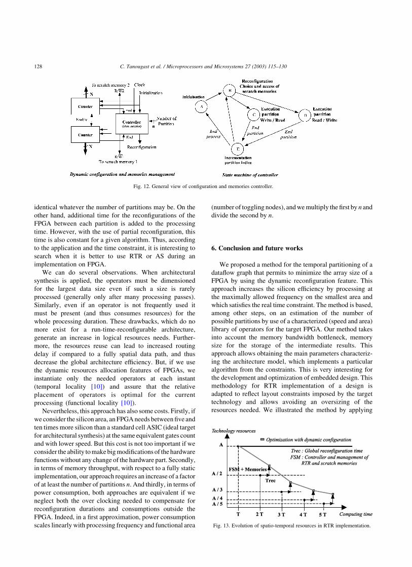
The controller needs two counters to address the
memories, a state machine for the control of the RTR and
the management of the memories for read or write access
(Fig. 12).
In our case, the controller consists in two 18 bit counters
(images of 5122 pixels), a state machine with five states, a 4
bit register to capture the number of partitions (we assume a
number of reconfiguration lower than 16), a counter
indicating the number of partitions, a 4 bit comparator and
a toggle flip–flop to indicate to which alternate buffer
memory we have to read and write. With the targeted FPGA
structure (see Section 4), the logic area of the controller in
each configuration stage requires a number of resources
lower than 50 logical cells. So, it is needed to add 50 cells to
each partition area given in Section 4.3.2.
4.3.4. Summary of needed resources
The resources characteristics of the platform to use or to
design for the first example algorithm are: Memory size:
256 Kwords of 30 bits, computing area (computing
reconfigurable area þ controller area): 209 cells, memory
bandwidth: 19 bits with a minimal read/write frequency of
24.8 MHz. For the second algorithm, the memory size and
the controller logic area are the same than for the previous
algorithm. However, in this case, the computing area needs
344 cells, memory bandwidth: 30 bits with a minimal
read/write frequency of 25.8 MHz.
5. Discussion
The objective of the Algorithm/Architecture Adequation
is to find best an efficient matching between an algorithm
and an architecture. The aim is to realize an optimal
implementation that satisfies the constraints (real time, logic
area, etc.). In this Section, we illustrate an analysis of the
gains and costs of the use of dynamic reconfiguration. We
can compare our method to the more classical architectural
synthesis, which is based on the reuse of operator by adding
control at different time [32,33]. Indeed, the goal of the two
approaches is the minimization of hardware resources with
respect to time constraint. If we consider our method with
respect to an architectural synthesis, the RTR can be
illustrated by Fig. 13.
Fig. 13 represents the needed area with respect to the
processing time for RTR. The optimization with AS can
divide by two the logical resources at the cost of an
additional cycle time for the processing. This observation
applies only if we do not take in account the controller and
memory resources that are needed for AS. These additional
resources are difficult to estimate in AS because they depend
heavily on the algorithm. In the case of RTR, if we consider
critical times identical to those of AS, we notice the same
optimization level. Nevertheless, the RTR control and
memory management (hidden or not in the FPGA) logical
resources are easy to deduce. Moreover, in contrast with AS
which sees its control increasing with the level of re-use of
the operators, these control resources remain relatively
Fig. 10. Ardoise module.
Table 7
Implementation results of edges detector with an AT40K
Partition
number
Number
of cells
Operator
execution
time (ns)
Partition
reconfiguration
time (ms)
Partition
processing
time (ms)
1 152 40.1 111 10.5
2 156 40.3 114 10.6
3 159 36.7 116 9.6
Table 8
Implementation results of the optical flow estimator with an AT40K
Partition
number
Number
of cells
Operator
execution
time (ns)
Partition
reconfiguration
time (ms)
Partition
processing
time (ms)
1 209 27.1 160 7. 1
2 354 38.7 260 10.15
3 336 37.8 250 9.91
Table 9
Implementation results of the normal optical flow estimator after refined
partitioning
Partition
number
Number
of cells
Operator
execution
time (ns)
Partition
reconfiguration
time (ms)
Partition
processing
time (ms)
1 209 27.1 160 7.1
2 241 38.7 180 10.15
3 248 38.7 180 10.15
4 294 37.8 190 9.91
C. Tanougast et al. / Microprocessors and Microsystems 27 (2003) 115–130126
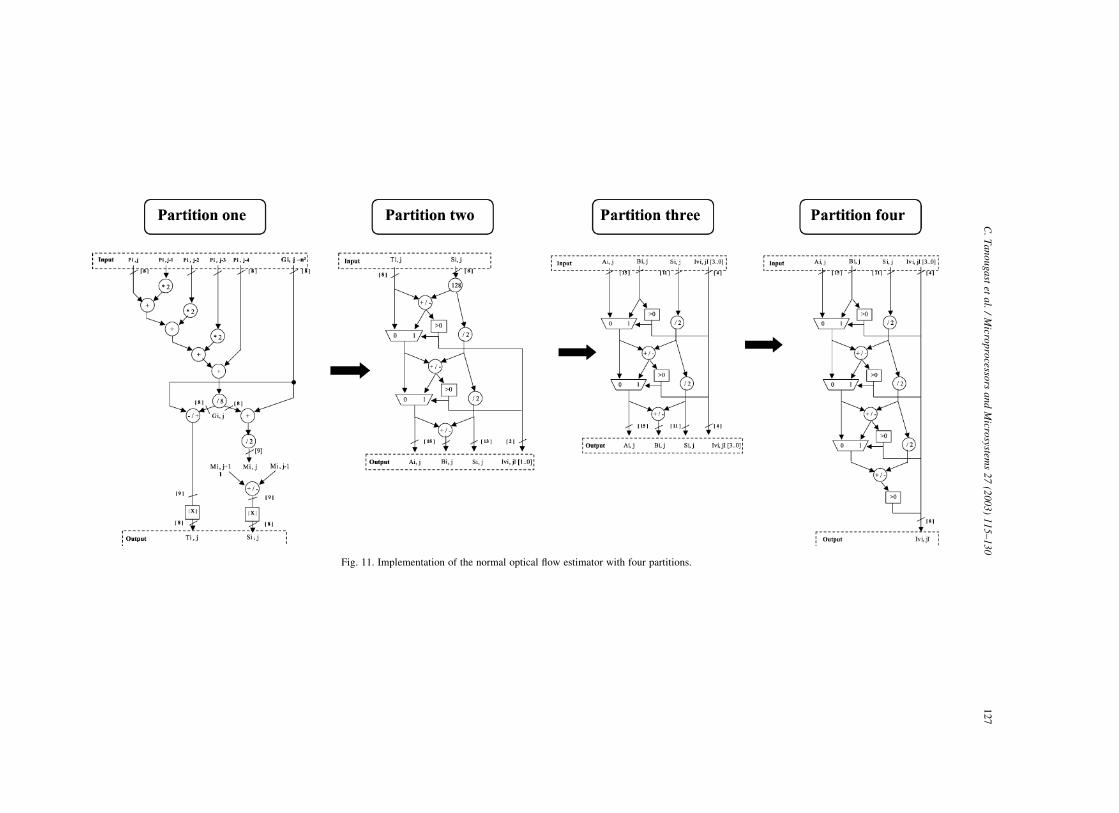
Fig. 11. Implementation of the normal optical flow estimator with four partitions.
C.
Ta
no
uga
stet
al.
/M
icrop
rocesso
rsa
nd
Micro
systems
27
(20
03
)1
15
–1
30
12
7
identical whatever the number of partitions may be. On the
other hand, additional time for the reconfigurations of the
FPGA between each partition is added to the processing
time. However, with the use of partial reconfiguration, this
time is also constant for a given algorithm. Thus, according
to the application and the time constraint, it is interesting to
search when it is better to use RTR or AS during an
implementation on FPGA.
We can do several observations. When architectural
synthesis is applied, the operators must be dimensioned
for the largest data size even if such a size is rarely
processed (generally only after many processing passes).
Similarly, even if an operator is not frequently used it
must be present (and thus consumes resources) for the
whole processing duration. These drawbacks, which do no
more exist for a run-time-reconfigurable architecture,
generate an increase in logical resources needs. Further-
more, the resources reuse can lead to increased routing
delay if compared to a fully spatial data path, and thus
decrease the global architecture efficiency. But, if we use
the dynamic resources allocation features of FPGAs, we
instantiate only the needed operators at each instant
(temporal locality [10]) and assure that the relative
placement of operators is optimal for the current
processing (functional locality [10]).
Nevertheless, this approach has also some costs. Firstly, if
we consider the silicon area, an FPGA needs between five and
ten times more silicon than a standard cell ASIC (ideal target
for architectural synthesis) at the same equivalent gates count
and with lower speed. But this cost is not too important if we
consider the ability to make big modifications of the hardware
functions without any change of the hardware part. Secondly,
in terms of memory throughput, with respect to a fully static
implementation, our approach requires an increase of a factor
of at least the number of partitions n. And thirdly, in terms of
power consumption, both approaches are equivalent if we
neglect both the over clocking needed to compensate for
reconfiguration durations and consumptions outside the
FPGA. Indeed, in a first approximation, power consumption
scales linearly with processing frequency and functional area
(number of toggling nodes), and we multiply the first by n and
divide the second by n.
6. Conclusion and future works
We proposed a method for the temporal partitioning of a
dataflow graph that permits to minimize the array size of a
FPGA by using the dynamic reconfiguration feature. This
approach increases the silicon efficiency by processing at
the maximally allowed frequency on the smallest area and
which satisfies the real time constraint. The method is based,
among other steps, on an estimation of the number of
possible partitions by use of a characterized (speed and area)
library of operators for the target FPGA. Our method takes
into account the memory bandwidth bottleneck, memory
size for the storage of the intermediate results. This
approach allows obtaining the main parameters characteriz-
ing the architecture model, which implements a particular
algorithm from the constraints. This is very interesting for
the development and optimization of embedded design. This
methodology for RTR implementation of a design is
adapted to reflect layout constraints imposed by the target
technology and allows avoiding an oversizing of the
resources needed. We illustrated the method by applying
Fig. 12. General view of configuration and memories controller.
Fig. 13. Evolution of spatio-temporal resources in RTR implementation.
C. Tanougast et al. / Microprocessors and Microsystems 27 (2003) 115–130128
it on two images processing algorithms and by real
implementation on the Atmel AT40K FPGA target
technology.
Our approach must be compared with other more
powerful optimizations tools such as simulated annealing,
genetic algorithms and so on. Currently we work on a
more accurate resources estimation which takes into
account the memory management part of the data path
and also checks if the available memory bandwidth is
sufficient. At this time, we started to computerize
(automate) the partition search procedure, called
DAGARD which means, in French, automatic partition-
ing of DFG for dynamically configurable systems, which
is roughly a graph covering function. Currently, only the
partition estimation part and boundaries generation
between each partitions is automated. Our perspectives
are an automatic synthesis of memory and configuration
controller by our tool. Indeed, from the partitions
computation, it is easy to automatically generate a
fixed-resources controller for a particular implementation.
Moreover, it is necessary to take into account the power
consumption that is an important parameter for
embedded systems design. This estimation depends on
the target technology and the working environment like
working frequency, resources needed for each partitions
[34,35]. However, it is mainly on the data-path part
(regular processing), that it is necessary to judge the
‘adequation’ of RTR for an implementation, because a
controller is more effectively produced by a program-
mable sequencer like a microprocessor. We also study
the possibilities to include an automatic architectural
solutions exploration for the implementation of arithmetic
operators.
Another future work is to find when it is better to use the
dynamic configuration or architectural synthesis for the
optimization of an implementation (see Section 5).
References
[1] S. Hauck, The role of FPGA in reprogrammable systems, Proceedings
of IEEE 86 (4) (1998) 615–638.
[2] S. Brown, J. Rose, FPGA and CPLD architectures: a tutorial, IEEE
Design and Test of Computers 13 (2) (1996) 42–57.
[3] S.A. Guccione, D. Levi, The advantages of run-time reconfigura-
tion, in: J. Schewel, P.M. Athanas, S.A. Guccione, S. Ludwig, J.T.
McHenry (Eds.), Reconfigurable Technology: FPGAs for Comput-
ing and Applications, Proceedings of SPIE 3844, SPIE—The
International Society for Optical Engineering, Bellingham, WA,
1999, pp. 87–92.
[4] P. Lysaght, J. Dunlop, Dynamic reconfiguration of FPGAs, in: W.
Moore, W. Luk (Eds.), More FPGA’s, Oxford, Abingdon, England,
1994, pp. 82–94.
[5] S.C. Goldstein, H. Schmit, M. Budiu, S. Cadambi, M. Moe, R. Taylor,
PipeRench: a reconfiguration architecture and compiler, IEEE
Computer April (2000).
[6] L. Kessal, D. Demigny, N. Boudouani, R. Bourguiba, Reconfigurable
hardware for real time image processing, Proceedings of the
International Conference on Image Processing, IEEE ICIP, Vancou-
ver 3 (2000) 159–173.
[7] B. Kastrup, A. Bink, J. Hoogerbrugge, ConCISe: a compiler-driven
CPLD-based instruction set accelerator, in: K.L. Pocek, J.M. Arnold
(Eds.), Proceedings of the Seventh Annual IEEE Symposium on Field-
Programmable Custom Computing Machines, 1999, pp. 92–101.
[8] J.E. Vuillemin, P. Bertin, D. Roncin, M. Shand, H.H. Touati, P.
Boucard, Programmable active memories: reconfigurable systems
come of age, IEEE Transactions on VLSI Systems 4 (1) (1996)
56–69.
[9] M.J. Wirthlin, B.L. Hutchings, A dynamic instruction set computer,
IEEE Symposium on FPGA’s Custom Computing Machines, Napa,
CA April (1995) 99–107.
[10] X. Zhang, K.W. Ng, A review of high-level synthesis for dynamically
reconfigurable FPGA’s, Microprocessors and Microsystems 24 (2000)
199–211. Elsevier.
[11] C. Tanougast, Methodologie de partitionnement applicable aux
systemes sur puce a base de FPGA, pour l’implantation en
reconfiguration dynamique d’algorithmes flot de donnees, PhD
Thesis, Faculte des Sciences, Universite de Nancy I, 2001.
[12] T.J. Callahan, J. Hauser, J. Wawrzynek, The GARP architecture and C
compiler, IEEE Computer 33 (4) (2000) 62–69.
[13] T.J. Callahan, P. Chong, A. DeHon, J. Wawrzynek, Fast module
mapping and placement for data paths in FPGA’s, Proceedings of
the ACM/SIGDA Sixth International Symposium on Field
Programmable Gate Arrays, Monterey, CA February (1998)
123–132.
[14] S.V. Srinivasan, S. Govindarajan, R. Vemuri, Fine-grained and
coarse-grained behavioral partitioning with effective utilization of
memory and design space exploration for multi-FPGA architectures,
IEEE Transactions on VLSI Systems 9 (1) (2001) 140–158.
[15] M. Kaul, R. Vemuri, Optimal temporal partitioning and synthesis
for reconfigurable architectures, International Symposium on Field-
Programmable Custom Computing Machines April (1998)
312–313.
[16] R. Maestre, F. Kurdahi, M. Fernadez, R. Hermida, N. Bagherzadeh, H.
Singh, A framework for reconfigurable computing: task scheduling
and context manegement, IEEE Transactions on VLSI Systems 9 (6)
(2001) 858–873.
[17] M. Karthikeya, P. Gajjala, B. Dinesh, Temporal partitioning and
scheduling data flow graphs for reconfigurable computer, IEEE
Transactions on Computers 48 (6) (1999) 579–590.
[18] N. Shirazi, W. Luk, P.Y.K. Cheung, Automating production of run-
time reconfiguration designs, in: K.L. Pocek, J. Arnold (Eds.),
Proceedings of IEEE Symposium on FPGA’s Custom Computing
Machines, IEEE Computer Society Press, 1998, pp. 147–156.
[19] W. Luk, N. Shirazi, P.Y.K. Cheung, Modeling and optimizing run-
time reconfiguration systems, in: K.L. Pocek, J. Arnold (Eds.),
Proceedings of IEEE Symposium on FPGA’s Custom Computing
Machines, IEEE Computer Society Press, 1996, pp. 167–176.
[20] P. Lysaght, J. Stockwood, A simulation tool for dynamically
reconfigurable field programmable gare arrays, IEEE Transactions
on VLSI Systems 4 (3) (1996) 381–390.
[21] M. Valsiko, DYNASTY: a temporal floorplanning based CAD
framework for dynamically reconfigurable logic systems, in: P.
Lysaght, J. Irvine, R. Hartenstein (Eds.), Lecture Notes in Computer
Science, vol. 1673, 1999, pp. 124–133, Glasgow, UK.
[22] A. Cataldo, Hybrid architecture embeds Xilinx FPGA core into IBM
ASICs, EE Times Jun 24, 2002, http://www.eetimes.com/story/
OEG20020624S0016.
[23] J. Becker, R. Hartenstein, M. Herz, U. Nageldinger, Parallelization in
co-compilation for configurable accelerators, proceedings of Asia and
South Pacific Design Automation Conference, ASP-DAC’98 Yoko-
hama, Japan (1998).
C. Tanougast et al. / Microprocessors and Microsystems 27 (2003) 115–130 129
[24] A. Dehon, Comparing computing machines, Proceedings of the SPIE
3526 (1998) 124–133.
[25] M.J. Wirthlin, B.L. Hutchings, Improving functional density using
run-time circuit reconfiguration, IEEE Transactions on VLSI Systems
6 (2) (1998) 247–256.
[26] J.G. Eldredge, B.L. Hutchings, Run-time reconfiguration: a method
for enhancing the functional density of SRAM-based FPGA’s,,
Journal of VLSI Signal Processing 12 (1996) 67–86.
[27] M. Vasilko, D. Ait-Boudaoud, Scheduling for dynamically reconfi-
gurable FPGAs, In Proceeding of International Workshop on Logic
and Architecture Synthesis, IFIP TC10 WG10.5, Grenoble, France
(1995) 328–336.
[28] D. Demigny, L. Kessal, R. Bourguiba, N. Boudouani, How to use high
speed reconfigurable fpga for real time image processing?, Proceed-
ings of IEEE Conference on Computer Architecture for Machine
Perception, IEEE Circuit and Systems, Padova September (2000)
240–246.
[29] N. Demassieux, Architecture VLSI pour le traitement d’images: Une
contribution a l’etude du traitement materiel de l’information, PhD
Thesis, Ecole nationale superieure des telecommunications (ENST),
1991.
[30] C. Tanougast, Y. Berviller, S. Weber, Optimization of motion
estimator for run-time reconfiguration implementation, in: J. Rolim
(Ed.), Parallel and Distributed Processing, Lecture Notes in Computer
Science, vol. 1800, Springer, 2000, pp. 959–965.
[31] Atmel AT40k Datasheet.
[32] N. Togawa, M. Ienaga, M. Yanagisawa, T. Ohtsuki, An area/time
optimizing algorithm in high-level synthesis for control-base hard-
wares, Proceedings of the ASP-DAC 2000, IEEE circuits and systems,
Yokohama, Japan (2000) 309–312.
[33] A. Sharma, R. Jain, Estimating architectural resources and perform-
ance for high-level synthesis applications, IEEE Transactions on
VLSI Systems 1 (2) (1993) 175–190.
[34] A. Bogliolo, R. Corgnati, E. Macii, M. Poncino, Parameterized RTL
power models for soft macros, IEEE Transactions on VLSI Systems 9
(6) (2001) 880–887.
[35] A. Garcia, W. Burleson, J.L. Danger, Power modelling in field
programmable gate arrays (FPGA), in: P. Lysaght, J. Irvine, R.
Hartenstein (Eds.), Lecture Notes in Computer Science, vol. 1673,
1999, pp. 396–404, Glasgow, UK.
Camel Tanougast received his PhD
degree in Microelectronic and Electronic
Instrumentation from the University of
Nancy 1, France in 2001. Currently is a
researcher in Electronic Instrumentation
Laboratory of Nancy (LIEN). His research
interests include: design and implemen-
tation real time processing architecture,
FPGA design and the Terrestrial Digital
Television (DVB-T).
Yves Berviller received the PhD degree
in electronic in 1998 from the Henri
Poincare University, Nancy, France. He
is currently assistant professor with Henri
Poincare University. His research inter-
ests include computing vision, system on
chip development and research, FPGA
design and the Terrestrial Digital Televi-
sion (DVB-T).
Philippe Brunet received an MSc
degree from the University of
Dijon, France in 2001. Currently,
he is a PhD research student in
Electronic Engineering at the Elec-
tronic Instrumentation Laboratory
of Nancy (LIEN), University of
Nancy 1. His main interest con-
cerns Design FPGA and computing
vision.
Serge Weber received the PhD. Degree in
electronic in 1986, from the University of
Nancy (France). In 1988 he joined the
Electronics Laboratory of Nancy (LIEN)
as an Associate Professor. Since Septem-
ber 1997 he is Professor and Manager of
the Electronic Architecture group at LIEN
(University Henri Poincare Nancy I). His
research interests are on reconfigurable
and parallel architectures for image and
signal processing or for intelligent sensors.
Hassan Rabah received the PhD
degree in electronic in 1992 from the
Henri Poincare University, Nancy,
France. He is currently assistant pro-
fessor with Henri Poincare University.
His research interests include system
on chip development and research,
digital signal processing and sensor
applications.
C. Tanougast et al. / Microprocessors and Microsystems 27 (2003) 115–130130


