Embed Size (px)
Citation preview
This article appeared in a journal published by Elsevier. The attachedcopy is furnished to the author for internal non-commercial researchand education use, including for instruction at the authors institution
and sharing with colleagues.
Other uses, including reproduction and distribution, or selling orlicensing copies, or posting to personal, institutional or third party
websites are prohibited.
In most cases authors are permitted to post their version of thearticle (e.g. in Word or Tex form) to their personal website orinstitutional repository. Authors requiring further information
regarding Elsevier’s archiving and manuscript policies areencouraged to visit:
http://www.elsevier.com/copyright

Author's personal copy
Structural dependence of piezoelectric, dielectric and ferroelectric properties ofK0.5Na0.5(Nb1�2x/5Cux)O3 lead-free ceramics with high Qm
Xiaohui Tan a,b, Huiqing Fan a,*, Shanming Ke b,c, Limin Zhou b, Yiu-Wing Mai b,d, Haitao Huang c,*a State Key Laboratory of Solidification Processing, School of Materials Science and Engineering, Northwestern Polytechnical University, Xi’an 710072, PR Chinab Department of Mechanical Engineering, The Hong Kong Polytechnic University, Hung Hum, Kowloon, Hong Kongc Department of Applied Physics and Materials Research Center, The Hong Kong Polytechnic University, Hung Hum, Kowloon, Hong Kongd Centre for Advanced Materials Technology, School of Aerospace, Mechanical and Mechatronics Engineering J07, The University of Sydney, Sydney, NSW 2006, Australia
1. Introduction
In the past decade, perovskite potassium sodium niobate(K,Na)NbO3 (KNN) family has attracted much attention as apromising candidate of lead-free piezoelectric materials. Goodpiezoelectric properties, such as a large piezoelectric constant,d33 = 416 pC/N, and a large planar coupling factor, kp = 0.61, havebeen observed in textured K0.5Na0.5NbO3-based ceramics [1]. Sincethen, a number of studies have been carried out to develop ‘‘soft’’and/or ‘‘hard’’ KNN-based piezoelectric ceramics for variouspractical applications.
Generally, soft piezoelectrics exhibit square hysteresis, largedielectric constant, large electromechanical coupling factor k, highpiezoelectric constant d33 and high dielectric losses tan d, whilehard piezoelectrics have lower k, d33, tan d and high mechanicalquality factor Qm [2]. Actually, hard piezoelectrics with high Qm areessentially required by many high-power and high-voltagedevices, such as ultrasonic motors and transformers [3]. Althoughthe mechanism of softening and hardening of the piezoelectricproperties is still not clearly understood, perovskite piezoelectricceramics can generally be hardened if doped with acceptor-typedopants, such as Fe3+, 2+ substituted onto Zr4+/Ti4+ sites [4,5]. It has
been reported that the addition of small amount of Cu compounds,e.g. CuO [6–8], K5.4Cu1.3Ta10O29 [10], and K4CuNb8O23 [11], whereCu2+ substitutes onto Nb5+ site as an acceptor, were effective inimproving the Qm of KNN ceramics. For KNN-based lead-freeceramics, a high mechanical quality factor (Qm = 2500) has beenreported in CuO-doped K0.5Na0.5NbO3 [6], which is much higherthan that of lead zirconium titanate (PZT).
In this paper, we present results of an experimental study on thestructure and property evolution of the Cu-substitutedK0.5Na0.5NbO3 ceramics with high mechanical quality factor.Typically, there are three types of formula for Cu doping: (1)K0.5Na0.5NbO3–x%CuO, where CuO is directly mixed with KNN, (2)K0.5Na0.5(Nb1�2x/5Cux)O3, and (3) K0.5Na0.5(Nb1�xCux)O3�d. In thelatter two types, Nb5+ is substituted by Cu2+. However, only thefirst and the third dopant type were reported in the literatures [6–9]. We, instead, focused on the second type formula in this workand prepared the ceramic samples by conventional solid statereaction process. The structural dependence of the ferroelectric,piezoelectric and dielectric properties was investigated anddiscussed in details.
2. Experimental
Ceramics with nominal composition (K0.5Na0.5)(Nb1�2x/5Cux)O3
(abbreviated as KNNC, x = 0, 0.25, 0.50, 0.75, 1.00, 1.25, 1.50, 1.75,and 2.00%, respectively,) were synthetized by conventional solidstate solution process. Analytical reagents of K2CO3, Na2CO3,
Materials Research Bulletin 47 (2012) 4472–4477
A R T I C L E I N F O
Article history:
Received 25 January 2012
Received in revised form 13 August 2012
Accepted 24 September 2012
Available online 2 October 2012
Keywords:
A. Ceramics
D. Piezoelectricity
D. Defects
A B S T R A C T
(K0.5Na0.5)(Nb1�2x/5Cux)O3 (abbreviated as KNNC, x = 0–2%) lead-free ceramics were synthetized by the
solid state solution method. Pure perovskite phase with orthorhombic symmetry was observed. The
evolution of the structure of KNNC was examined by X-ray diffraction (XRD), scanning electron
microscopy (SEM) and Raman scattering spectra techniques. Our results revealed that, defect dipoles
ðCu000Nb�VO��Þ0 were formed and provided a restoring force to reverse the switched polarization, which
resulted in double P–E hysteresis loops in KNNC with Cu doping at x = 0.75% and 1%. However, non-polar
defect complex ðVO���Cu000Nb�VO
��Þ� caused a lattice shrinkage and the observed square shaped P–E loops
in KNNC ceramics under high doping levels (x > 1%).
� 2012 Elsevier Ltd. All rights reserved.
* Corresponding authors.
E-mail addresses: [email protected] (H. Fan), [email protected]
(H. Huang).
Contents lists available at SciVerse ScienceDirect
Materials Research Bulletin
jo u rn al h om ep age: ww w.els evier .c o m/lo c ate /mat res b u
0025-5408/$ – see front matter � 2012 Elsevier Ltd. All rights reserved.
http://dx.doi.org/10.1016/j.materresbull.2012.09.049

Author's personal copy
Nb2O5, and CuO were mixed by a planetary ball mill usinganhydrous ethanol as the media, and then calcined at 850 8C for2.5 h. After calcination, the mixture was ball milled again and thenpressed into disks of 15 mm in diameter and 1.5 mm in thicknessunder a cold-isostatic pressure of 300 MPa for 90 s. These Cu-doped green pallets were sintered at 1070 8C for 4 h, while pureKNN pellets were sintered at 1090 8C for 4 h, and all in a K/Na richambient.
The crystalline structure of KNNC ceramics was determined byX-ray diffraction (XRD; D/Max2550VB+/PC, Rigaku Co., Tokyo,Japan) with Cu Ka radiation on powder samples. The structure ofKNNC ceramics was studied by scanning electron microscope(SEM; 6700F, JEOL, Tokyo, Japan). Micro-Raman spectrum mea-surements were performed on a Raman spectrometer underbackscattering geometry (HR800, Jobin Yvon, Paris, France). AnArgon ion laser was used as the excitation source with an outputpowder of 15 mW at 488 nm.
Top and bottom electrodes were made by coating silver painton both sides of the sintered and polished ceramic disks,followed by annealing at 550 8C for 20 min. For piezoelectricmeasurement, the ceramics were poled under a dc field of 3 kV/mm at 130 8C in a silicone oil bath for 20 min. Temperaturedependences of the complex dielectric permittivity as well as thedc conductivity of KNNC ceramics were measured using aprecision impedance analyzer (4294A, Agilent, Santa Clara, CA,USA) and a high-resistance meter (4339B, Agilent, Santa Clara,CA, USA) in a temperature range of 25–480 8C controlled by aprogram controller (TP-95, Linkam, Surrey, UK). The ferroelectrichysteresis loops (P–E loops) as well as electrostrictive strains (S–E loops) were examined by using a standard ferroelectricanalyzer (TF-2000, aixACCT, Aachen, Germany). The piezoelec-tric coefficient (d33) was measured by a piezoelectric d-meter(ZJ-4NA, Institute of Acoustics, Chinese Academy of Science,Beijing, China). The electromechanical coupling factor (kp) andthe mechanical quality factor (Qm) were obtained by theresonance method according to the IEEE Standard 176 using aprecision impedance analyzer (4294A, Agilent, Santa Clara, CA,USA).
3. Results and discussion
Fig. 1(a) shows the XRD patterns of the KNNC samples. It can beseen that all the KNNC ceramics present a pure perovskite phase atroom temperature and no secondary phase can be detected. Thecrystalline structure was orthorhombic (JCPDS-32-0822), featuredby the splitting of the (1 1 0)/(0 0 1) and (2 2 0)/(0 0 2) peaks withhigher intensity counts for the (1 1 0) and (2 2 0) reflections. Withincreasing Cu2+ concentration, the splitting of (1 1 0)/(0 0 1) and(2 2 0)/(0 0 2) orthorhombic reflections became more significant,implying that the dopant was incorporated into the perovskitelattice to form a solid solution. It can be concluded that thesolubility limit of Cu in KNN is more than 2%.
Fig. 1(b) and (c) presents the evolution of the intensity ratio ofthe two characteristic diffraction peaks I(2 2 0)/I(0 0 2) and the latticeparameters ratio c/a. The c/a ratio, as well as the unit-cell volume V,increases with increasing amount of Cu2+ for x < 1%. They start todecrease with Cu increasing to higher concentration. The evolutionin c/a and V suggests a transition behavior in the incorporation of
Fig. 1. (a) XRD patterns of the KNNC ceramics, (b) intensity ratio of diffraction peak I(2 2 0)/I(0 0 2) and (c) evolution of the lattice parameter ratio c/a with x = 0.25–2.0%.
Fig. 2. Schematic representation of the defect structure in KNNC: (a) ðCu000Nb�VO��Þ0
with a lower Cu concentration and (b) ðVO���Cu000Nb�VO
��� with a higher Cu
concentration. PD is the polarization associated with the ðCu000Nb�VO��Þ0 complex.
X. Tan et al. / Materials Research Bulletin 47 (2012) 4472–4477 4473
Author's personal copy
Cu2+ ions into the lattice, which can be explained as follows. SinceCu2+ has a relatively larger ionic radius than that of Nb5+ (0.73 and0.64 A for Cu2+ and Nb5+, respectively), lattice expansion isgenerally expected as Cu2+ gradually enters into the lattice. Onthe other hand, the formation of oxygen vacancies for chargecompensation tends to shrink the lattice. The competition betweenthe two effects results in the observed variation of c/a ratio and theunit-cell volume V with respect to the Cu concentration. As will beexplained below, when x < 1%, ðCu000Nb�VO
��Þ0 is the dominantdefect complex formed, while for x > 1.25%, ðVO
���Cu000Nb�VO���
will dominate.Electron paramagnetic resonance (EPR) and first-principles
calculation show that, in KNN [13–16], Cu2+ preferentially occupiesthe Nb5+ site where it can trap one or two oxygen vacancies.Correspondingly, two types of defect associates can be formed,ðCu000Nb�VO
��Þ0 and ðVO���Cu000Nb�VO
��� as shown in Fig. 2. Thetrimeric complex will cause larger lattice shrinkage than that of
dimeric complex. A transition of the dominant defect complexfrom ðCu000Nb�VO
��Þ0 to ðVO���Cu000Nb�VO
��� takes place at aroundx = 1%, which successfully explain the results shown in Fig. 1(c).However, we should not exclude the possibility of the incorpo-ration of Cu2+ onto A-site due to the volatility of K and Na [8], whichcould also decreased the unit-cell volume since the ionic radius ofCu2+ is smaller than K+ and Na+ (1.52 and 1.16 A for K+ and Na+,respectively) [12].
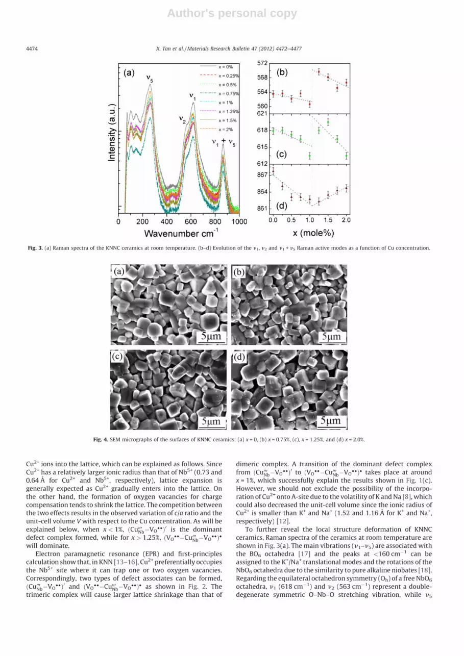
To further reveal the local structure deformation of KNNCceramics, Raman spectra of the ceramics at room temperature areshown in Fig. 3(a). The main vibrations (n1–n5) are associated withthe BO6 octahedra [17] and the peaks at <160 cm�1 can beassigned to the K+/Na+ translational modes and the rotations of theNbO6 octahedra due to the similarity to pure alkaline niobates [18].Regarding the equilateral octahedron symmetry (Oh) of a free NbO6
octahedra, n1 (618 cm�1) and n2 (563 cm�1) represent a double-degenerate symmetric O–Nb–O stretching vibration, while n5
Fig. 3. (a) Raman spectra of the KNNC ceramics at room temperature. (b–d) Evolution of the n1, n2 and n1 + n5 Raman active modes as a function of Cu concentration.
Fig. 4. SEM micrographs of the surfaces of KNNC ceramics: (a) x = 0, (b) x = 0.75%, (c), x = 1.25%, and (d) x = 2.0%.
X. Tan et al. / Materials Research Bulletin 47 (2012) 4472–44774474
Author's personal copy
(265 cm�1) means a triply degenerate symmetric O–Nb–O bendingvibration [19–22]. Fig. 3(b)–(d) shows the shift of n1, n2 and n1 + n5
modes of the Raman spectra of KNNC ceramics with Cuconcentration. It can be seen that the peak shift for all the n1, n2
and n1 + n5 modes has a discontinuity at around x = 1%. Thisobservation agrees well with the XRD results shown in Fig. 1. Theshift of the stretching mode (n1, n2) to lower frequencies withincreasing amount of Cu doping is due to a weakening of bondstrength caused by the oxygen vacancies. The Full width at halfmaximum of n1+5 keeps at 40–45 cm�1, this indicates good particleconsistency of KNNC ceramics.
Fig. 4 shows the SEM micrographs of the surfaces of KNNCceramics. The relative densities of all the samples are within therange of 92–97%. It is noted that CuO is an excellent sintering aid inmany material systems [23]. With the doping of CuO, the sinteringtemperature of KNNC ceramics can be lowered from 1090 to1070 8C. The KNNC ceramics have uniform grains with a grain sizein the range of 2–3.5 mm.
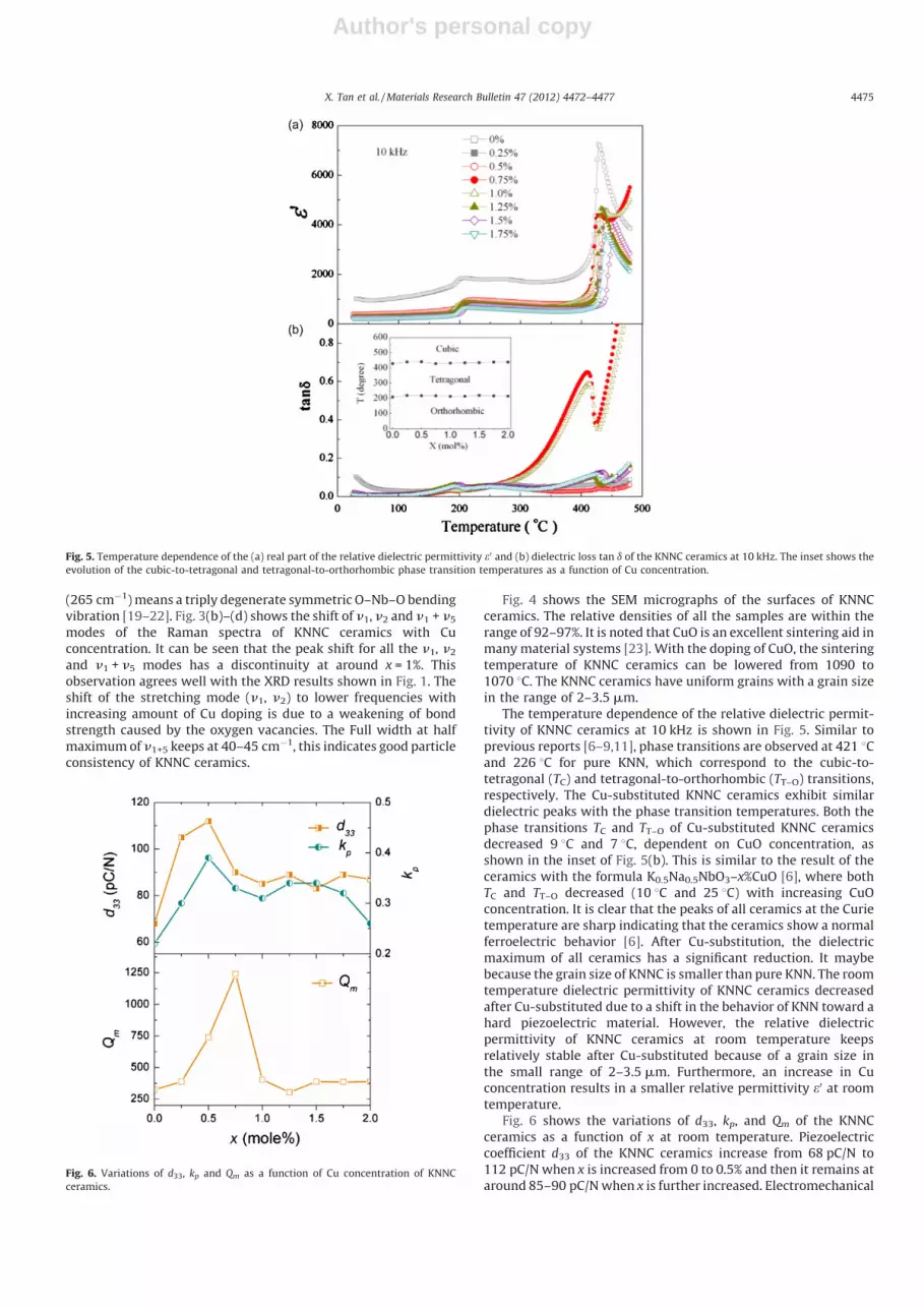
The temperature dependence of the relative dielectric permit-tivity of KNNC ceramics at 10 kHz is shown in Fig. 5. Similar toprevious reports [6–9,11], phase transitions are observed at 421 8Cand 226 8C for pure KNN, which correspond to the cubic-to-tetragonal (TC) and tetragonal-to-orthorhombic (TT–O) transitions,respectively. The Cu-substituted KNNC ceramics exhibit similardielectric peaks with the phase transition temperatures. Both thephase transitions TC and TT–O of Cu-substituted KNNC ceramicsdecreased 9 8C and 7 8C, dependent on CuO concentration, asshown in the inset of Fig. 5(b). This is similar to the result of theceramics with the formula K0.5Na0.5NbO3–x%CuO [6], where bothTC and TT–O decreased (10 8C and 25 8C) with increasing CuOconcentration. It is clear that the peaks of all ceramics at the Curietemperature are sharp indicating that the ceramics show a normalferroelectric behavior [6]. After Cu-substitution, the dielectricmaximum of all ceramics has a significant reduction. It maybebecause the grain size of KNNC is smaller than pure KNN. The roomtemperature dielectric permittivity of KNNC ceramics decreasedafter Cu-substituted due to a shift in the behavior of KNN toward ahard piezoelectric material. However, the relative dielectricpermittivity of KNNC ceramics at room temperature keepsrelatively stable after Cu-substituted because of a grain size inthe small range of 2–3.5 mm. Furthermore, an increase in Cuconcentration results in a smaller relative permittivity e0 at roomtemperature.
Fig. 6 shows the variations of d33, kp, and Qm of the KNNCceramics as a function of x at room temperature. Piezoelectriccoefficient d33 of the KNNC ceramics increase from 68 pC/N to112 pC/N when x is increased from 0 to 0.5% and then it remains ataround 85–90 pC/N when x is further increased. Electromechanical
Fig. 6. Variations of d33, kp and Qm as a function of Cu concentration of KNNC
ceramics.
Fig. 5. Temperature dependence of the (a) real part of the relative dielectric permittivity e0 and (b) dielectric loss tan d of the KNNC ceramics at 10 kHz. The inset shows the
evolution of the cubic-to-tetragonal and tetragonal-to-orthorhombic phase transition temperatures as a function of Cu concentration.
X. Tan et al. / Materials Research Bulletin 47 (2012) 4472–4477 4475

Author's personal copy
coupling factor kp shows a similar trend as d33, giving a maximumvalue of 39% at x = 0.5%. It can also be found that theelectromechanical quality factor Qm of KNNC ceramics is highlydependent of Cu doping content. Although Qm of pure KNN ceramicsis 325, it increases sharply up to 1241 with the addition of 0.75%Cu2+. As mentioned above, Cu2+ preferentially occupies Nb5+ site andtraps oxygen vacancy to form the defect complex ðCu000Nb�VO
��Þ0 [13–16]. This defect complex ðCu000Nb�VO
��Þ0 contains an electric dipolemoment PD (Fig. 2(a)), which can re-orient itself under the dipole–dipole interaction with the spontaneous polarization for theminimization of energy, leading to a high Qm as those observed inPZT [24]. The dramatic decrease of Qm when x > 1% can be ascribed tothe formation of the trimeric complex ðVO
���Cu000Nb�VO���, which
contains no electric dipole moment.Fig. 7 shows the room temperature P–E and S–E loops at 1 Hz for
the ceramics with x = 0–1.75%. Pure KNN demonstrates a typical‘‘square’’ ferroelectric hysteresis single loop, and a butterfly-shaped S–E loop. A striking feature of the P–E loop is that, as x
increases, it becomes constricted and turns into a double hysteresisloop although KNNC in this composition range is not antiferro-electric. Further increase in Cu-doping (x > 1%) recovers the P–E
loop to a ‘‘square’’ and well-saturated one. Similar double P–E loopshave also been observed in K0.5Na0.5NbO3–x%CuO ceramics [6–8].Lin et al. [6] stated that the observed double loops inK0.5Na0.5NbO3–x%CuO ceramics follow the same ‘‘symmetry-conforming principle’’ of point defects as those in aged ferroelectrictitanates. However, aging is not required in our case. In our case, forx � 1%, the defect complex ðCu000Nb�VO
��Þ0 with a dipole momenttends to arrange itself in an ‘‘antiparallel’’ direction to thespontaneous polarization (not exactly antiparallel, but formingan angle within 90–1808) when cooled from cubic to tetragonalphase. The hysteresis loop thus resembles that of an antiferro-electric. For KNNC ceramics with x > 1%, the dominate defectcomplex is ðVO
���Cu000Nb�VO��� which has no polarization and thus
‘‘square’’ P–E loops are observed.It should be noted that an earlier work [3] suggested that space
charge effect could be responsible for the double hysteresis loopand ‘‘hardening’’ behavior. It was claimed that the space chargesaccumulated at domain boundaries will create an internal electric
field along the direction of the spontaneous polarization to forcethe polarization to switch back to its original orientation when theexternal electric field is removed. This mechanism is notappropriate to explain the double hysteresis loops in KNNCceramics which are symmetrical (Fig. 7). Neither can it explains therecovery from a double loop to a ‘‘square’’ one when x > 1%.
For perovskite ferroelectrics, the dc conductivity at highertemperature range as well as the dielectric loss peak around Curietemperature is mainly attributed to the electromigration of oxygenvacancies [25,26]. Fig. 8 shows the measured dc conductivity in thetemperature range of 25–480 8C for KNNC ceramics with x = 0, 0.5,0.75, 1.0, 1.25 and 1.5%, respectively. The dashed lines are thefitting curves according to the Arrhenius equation t = t0 exp(� Ea/kBTm). The calculated activation energies (Ea) are shown in Fig. 8and are consistent with earlier reported values for perovskiteoxides [4,27]. Clearly, KNNC with x = 0.75% has the highestactivation energy Ea among the three samples, indicatingkinetically difficult migration of oxygen vacancies. It implies thatthe point defects in KNNC with x = 0.75% has a stronger ‘‘pining
Fig. 7. P–E and S–E hysteresis loops at 1 Hz for the KNNC ceramics with x = 0–1.75%.
Fig. 8. Arrhenius plot of the dc conductivity of KNNC ceramics with x = 0, 0.75, and
1.5%.
X. Tan et al. / Materials Research Bulletin 47 (2012) 4472–44774476

Author's personal copy
effect’’ than the other two and the KNNC ceramic sample is‘‘hardened’’. This may be coincided with the large dielectric losspeak emerged around Curie temperature in KNNC at x = 0.75% asgiven in Fig. 5(b). On the other hand, the conductivity firstlyincreases with Cu concentration increasing (x < 1%), then dropdown with Cu concentration increasing (x > 1%), and the maxvalue appear at x = 1.0%. It also indicates that the two types ofdipole conduction effects result from the formation of oxygenvacancies with different Cu doping concentrations.
4. Conclusions
Cu-substituted KNN ceramics have been prepared by a solidstate solution process. All the ceramics possess a perovskitestructure with orthorhombic symmetry at room temperature. TheXRD and Raman analysis reveal that there is a structuraldiscontinuity between x = 1% and x = 1.25%, which is mainly dueto the formation of different defect configurations. When thecontent of Cu is below 1%, the P–E loop of KNNC becomesconstricted and resembles a double-loop. It then recovers to anormal square loop when the concentration of Cu is furtherincreased. It is suggested that, for x � 1%, dimeric defect complexðCu000Nb�VO
��Þ0 with a dipole moment was formed, providing arestoring force to reverse the switched polarization. Meanwhile,the defect dipoles also provide a pining effect that makes theceramics hardened. When x > 1%, non-polar trimeric defectcomplex ðVO
���Cu000Nb�VO��� becomes dominate and the ceramics
display normal square hysteresis loops. The maximum mechanicalquality factor (Qm = 1241) was obtained in KNNC ceramics withx = 0.75%.
Acknowledgments
This work was supported by the National Nature ScienceFoundation (51172187), the SPDRF (20116102130002) and 111Program (B08040) of MOE, the Xi’an Science and Technology
Foundation (XA-AM-201003) and the Hong Kong PolytechnicUniversity (A-PL54 and 1-BD08). X.H. Tan would like to thank thefinancial support from NPU short-research visiting abroadprogram for her working at The Hong Kong Polytechnic University.
References
[1] Y. Saito, H. Takao, T. Tani, T. Nonoyama, K. Takatori, T. Homma, T. Nagaya, M.Nakamura, Nature 432 (2004) 84–87.
[2] M.I. Morozov, D. Damjanovic, J. Appl. Phys. 107 (2010), 034106-1–10.[3] E. Li, H. Kakemoto, S. Wada, T. Tsurumi, IEEE Trans. Ultrason. Ferroelectr. Freq.
Control 55 (2008) 980–987.[4] K. Carl, K.H. Hardtl, Ferroelectrics 17 (1978) 473–486.[5] S. Takahashi, Ferroelectrics 41 (1982) 143–156.[6] D.M. Lin, K.W. Kwok, H.L.W. Chan, J. Phys. D: Appl. Phys. 41 (2008), 045401-1–6.[7] E.M. Alkoy, M. Papila, Ceram. Int. 369 (2010) 1921–1927.[8] B.C. Park, I.K. Hong, H.D. Jang, V.D.N. Tran, W.P. Tai, J.S. Lee, Mater. Lett. 64 (2010)
1577–1579.[9] A. Cardin, B. Wessler, K. Benkert, C. Schuh, W.F. Maier, J. Electroceram. 19 (2007)
267–272.[10] M. Matsubara, K. Kikuta, S. Hirano, J. Appl. Phys. 97 (2005), 114105-1–7.[11] M. Matsubara, T. Yamaguchi, K. Kikuta, S. Hirano, Jpn. J. Appl. Phys. 43 (2004)
7159–7196.[12] R.D. Shannon, Acta Cryst. A32 (1976) 751–767.[13] R.A. Eichel, E. Erunal, M.D. Drahus, D.M. Smyth, J. Tol, J. Acker, H. Kungl, M.J.
Hoffmann, Phys. Chem. Chem. Phys. 11 (2009) 8698–8705.[14] R.A. Eichel, Phys. Chem. Chem. Phys. 13 (2011) 368–387.[15] E. Erunal, R.A. Eichel, Funct. Mater. Lett. 3 (2010) 19–24.[16] S. Korbel, P. Marton, C. Elsasser, Phys. Rev. B 81 (2010) 174115.[17] S.D. ROSS, J. Phys. C: Solid State Phys. 3 (1970) 1785–1790.[18] Y. Shiratori, A. Magrez, C. Pithan, Chem. Phys. Lett. 391 (2004) 288–292.[19] K. Kakimoto, K. Akao, Y.P. Guo, H. Ohsato, Jpn. J. Appl. Phys. 44 (2005) 7064–7067.[20] C.W. Ahn, H.I. Hwang, K.S. Lee, B.M. Jin, S. Park, G. Park, D. Yoon, H. Cheong, H.J.
Lee, I.W. Kim, Jpn. J. Appl. Phys. 49 (2010) 095801.[21] F. Rubio-Marcos, P. Marchet, T. Merle-Mejean, J.F. Fernandez, Mater. Chem. Phys.
123 (2010) 91–97.[22] E. Buixaderas, D. Nuzhnyy, I. Gregora, S. Kamba, M. Berta, B. Malic, M. Kosec, IEEE
Trans. Ultrason. Ferroelectr. Freq. Control 56 (2009) 1843–1849.[23] L.B. Kong, J. Ma, H. Huang, T.S. Zhang, F. Boey, Mater. Lett. 57 (2003) 3660–3667.[24] Q. Tan, J. Li, D. Viehland, Appl. Phys. Lett. 75 (1999) 418–420.[25] S. Steinsvik, R. Bugge, J. Gjonnes, J. Tafto, T. Norby, J. Phys. Chem. Solids 58 (1997)
969–976.[26] H. Fan, G. Park, J. Choi, H. Kim, Appl. Phys. Lett. 79 (2001) 1658.[27] C. Ang, Z. Yu, L.E. Cross, Phys. Rev. B 62 (2000) 228.
X. Tan et al. / Materials Research Bulletin 47 (2012) 4472–4477 4477


