Embed Size (px)
Citation preview
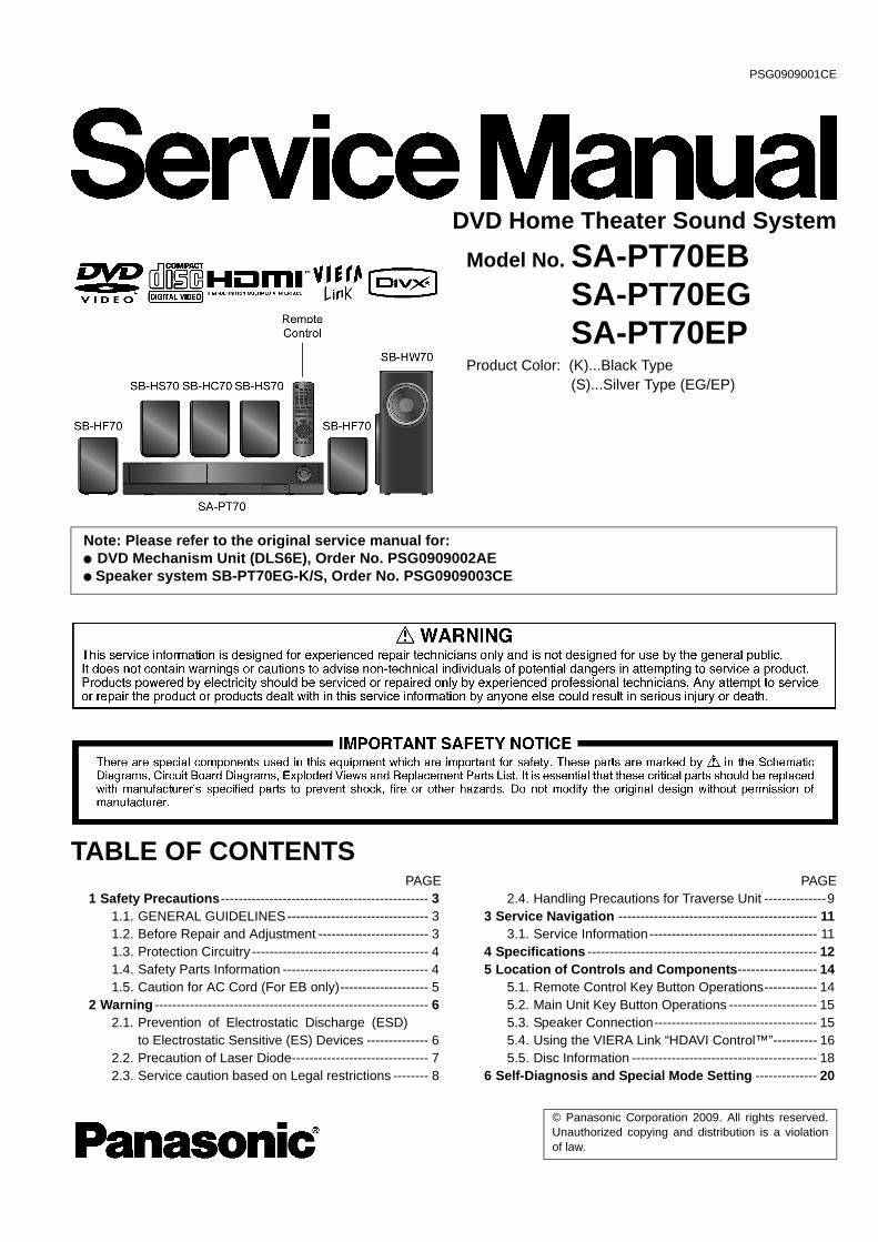
PSG0909001CE
DVD Home Theater Sound System
Model No. SA-PT70EBSA-PT70EGSA-PT70EP
Product Color: (K)...Black Type(S)...Silver Type (EG/EP)
TABLE OF CONTENTSPAGE PAGE
1 Safety Precautions----------------------------------------------- 31.1. GENERAL GUIDELINES-------------------------------- 31.2. Before Repair and Adjustment ------------------------- 31.3. Protection Circuitry ---------------------------------------- 41.4. Safety Parts Information --------------------------------- 41.5. Caution for AC Cord (For EB only)-------------------- 5
2 Warning -------------------------------------------------------------- 62.1. Prevention of Electrostatic Discharge (ESD)
to Electrostatic Sensitive (ES) Devices -------------- 62.2. Precaution of Laser Diode------------------------------- 72.3. Service caution based on Legal restrictions -------- 8
2.4. Handling Precautions for Traverse Unit --------------93 Service Navigation --------------------------------------------- 11
3.1. Service Information-------------------------------------- 114 Specifications ---------------------------------------------------- 125 Location of Controls and Components------------------ 14
5.1. Remote Control Key Button Operations------------ 145.2. Main Unit Key Button Operations -------------------- 155.3. Speaker Connection------------------------------------- 155.4. Using the VIERA Link “HDAVI Control™”---------- 165.5. Disc Information ------------------------------------------ 18
6 Self-Diagnosis and Special Mode Setting -------------- 20
Note: Please refer to the original service manual for: DVD Mechanism Unit (DLS6E), Order No. PSG0909002AE Speaker system SB-PT70EG-K/S, Order No. PSG0909003CE
© Panasonic Corporation 2009. All rights reserved.Unauthorized copying and distribution is a violationof law.
6.1. Cold-Start--------------------------------------------------- 206.2. Service Mode Table-------------------------------------- 206.3. Self-Diagnosis Mode ------------------------------------ 266.4. DVD Self Diagnostic Function-Error Code--------- 276.5. Sales Demonstration Lock Function ---------------- 306.6. Firmware Version-Up Information-------------------- 31
7 Troubleshooting Guide---------------------------------------- 347.1. Troubleshooting Guide for F61 and/or F76 -------- 347.2. Basic Troubleshooting Guide for Traverse
Unit (DVD Module P.C.B.)------------------------------ 387.3. Basic Troubleshooting Guide for HDMI AV
output-------------------------------------------------------- 398 Disassembly and Assembly Instructions --------------- 41
8.1. Disassembly Flow Chart-------------------------------- 428.2. Main Components and P.C.B. Locations ----------- 438.3. Disassembly of Top Cabinet--------------------------- 448.4. Disassembly of Scart P.C.B.--------------------------- 448.5. Disassembly of Rear Panel---------------------------- 458.6. Disassembly of DVD Mechanism Unit
(DLS6E) ---------------------------------------------------- 458.7. Disassembly of DVD Module P.C.B.----------------- 478.8. Disassembly of SMPS P.C.B. ------------------------- 488.9. Replacement of Switching Regulator IC
(IC5701) ---------------------------------------------------- 498.10. Replacement of Diode (D5802) ---------------------- 498.11. Disassembly of Main/D-Amp P.C.B. ----------------- 508.12. Replacement of Digital Amplifier IC (IC403/
IC404/IC405) ---------------------------------------------- 528.13. Disassembly of Front Panel Assembly ------------- 538.14. Disassembly of FL P.C.B. ------------------------------ 548.15. Disassembly of Volume Button P.C.B. -------------- 558.16. Disassembly of Power Button P.C.B.---------------- 568.17. Replacement of DVD Lid Assembly ----------------- 57
9 Assembling and Disassembling of Traverse Unit---- 609.1. Disassembly of Traverse Unit------------------------- 609.2. Assembly of Traverse Unit----------------------------- 61
10 Service Position ------------------------------------------------- 6210.1. Checking & Repairing Main/D-Amp P.C.B. &
Scart P.C.B.------------------------------------------------ 6210.2. Checking & Repairing of SMPS P.C.B. ------------- 6210.3. Checking & Repairing of FL P.C.B. ------------------ 6310.4. Checking & Repairing of DVD Module P.C.B.----- 63
11 Voltage & Waveform Chart ----------------------------------- 6611.1. DVD Module P.C.B. (1/4)------------------------------- 6611.2. DVD Module P.C.B. (2/4)------------------------------- 6711.3. DVD Module P.C.B. (3/4)------------------------------- 6811.4. DVD Module P.C.B. (4/4)------------------------------- 6811.5. Main P.C.B. (1/3) ----------------------------------------- 6911.6. Main P.C.B. (2/3) ----------------------------------------- 7011.7. Main P.C.B. (3/3) ----------------------------------------- 7111.8. FL P.C.B. --------------------------------------------------- 7211.9. SMPS P.C.B. ---------------------------------------------- 72
11.10. Scart P.C.B.------------------------------------------------ 7311.11. Waveform Table (1/3) ----------------------------------- 7411.12. Waveform Table (2/3) ----------------------------------- 7511.13. Waveform Table (3/3) ----------------------------------- 76
12 Illustration of ICs, Transistor and Diode ---------------- 7713 Overall Simplified Block Diagram ------------------------- 7914 Block Diagram --------------------------------------------------- 80
14.1. DVD(Servo)------------------------------------------------ 8014.2. DVD(Audio/Video) --------------------------------------- 81
14.3. DVD(UP-CON) ------------------------------------------- 8214.4. System Control ------------------------------------------- 8314.5. Analog Audio---------------------------------------------- 8414.6. Digital Audio----------------------------------------------- 8514.7. Analog Video---------------------------------------------- 8614.8. Power Supply--------------------------------------------- 87
15 Wiring Connection Diagram -------------------------------- 8916 Schematic Diagram Notes ----------------------------------- 9117 Schematic Diagram -------------------------------------------- 93
17.1. DVD Module Circuit ------------------------------------- 9317.2. Main/D-Amp Circuit ------------------------------------- 9817.3. FL, Volume Button & Power Button Circuit-------10417.4. Scart Circuit ----------------------------------------------10517.5. SMPS Circuit---------------------------------------------106
18 Printed Circuit Board-----------------------------------------10818.1. DVD Module P.C.B. ------------------------------------10818.2. Main/D-Amp P.C.B.-------------------------------------10918.3. FL, Volume Button, Power Button & Scart
P.C.B. ------------------------------------------------------ 11118.4. SMPS P.C.B.--------------------------------------------- 112
19 Terminal Function of ICs ------------------------------------ 11319.1. IC200 (RFKWMPT70EGK): IC
MICROPROCESSOR --------------------------------- 11319.2. IC901(C0HBB0000057): IC FL Driver------------- 113
20 Exploded View and Replacement Parts List---------- 11520.1. Exploded View and Mechanical Replacement
Part List --------------------------------------------------- 11520.2. Electrical Replacement Part List -------------------- 119
2
1 Safety Precautions1.1. GENERAL GUIDELINES
1. When servicing, observe the original lead dress. If a short circuit is found, replace all parts which have been overheated ordamaged by the short circuit.
2. After servicing, see to it that all the protective devices such as insulation barriers, insulation papers shields are properlyinstalled.
3. After servicing, carry out the following leakage current checks to prevent the customer from being exposed to shock hazards.
1.1.1. LEAKAGE CURRENT COLD CHECK1. Unplug the AC cord and connect a jumper between the two prongs on the plug.2. Measure the resistance value, with an ohmmeter, between the jumpered AC plug and each exposed metallic cabinet part on
the equipment such as screwheads, connectors, control shafts, etc. When the exposed metallic part has a return path to thechassis, the reading should be between 1MΩ and 5.2MΩ.When the exposed metal does not have a return path to the chassis, the reading must be
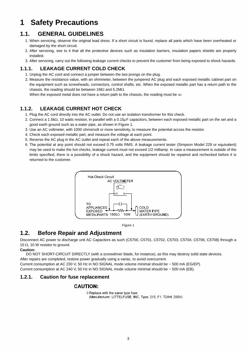
1.1.2. LEAKAGE CURRENT HOT CHECK1. Plug the AC cord directly into the AC outlet. Do not use an isolation transformer for this check.2. Connect a 1.5kΩ, 10 watts resistor, in parallel with a 0.15µF capacitors, between each exposed metallic part on the set and a
good earth ground such as a water pipe, as shown in Figure 1.3. Use an AC voltmeter, with 1000 ohms/volt or more sensitivity, to measure the potential across the resistor.4. Check each exposed metallic part, and measure the voltage at each point.5. Reverse the AC plug in the AC outlet and repeat each of the above measurements.6. The potential at any point should not exceed 0.75 volts RMS. A leakage current tester (Simpson Model 229 or equivalent)
may be used to make the hot checks, leakage current must not exceed 1/2 milliamp. In case a measurement is outside of thelimits specified, there is a possibility of a shock hazard, and the equipment should be repaired and rechecked before it isreturned to the customer.
Figure 1
1.2. Before Repair and AdjustmentDisconnect AC power to discharge unit AC Capacitors as such (C5700, C5701, C5702, C5703, C5704, C5706, C5708) through a10 Ω, 10 W resistor to ground.Caution:
DO NOT SHORT-CIRCUIT DIRECTLY (with a screwdriver blade, for instance), as this may destroy solid state devices.After repairs are completed, restore power gradually using a variac, to avoid overcurrent.Current consumption at AC 230 V, 50 Hz in NO SIGNAL mode volume minimal should be ~ 500 mA (EG/EP).Current consumption at AC 240 V, 50 Hz in NO SIGNAL mode volume minimal should be ~ 500 mA (EB).
1.2.1. Caution for fuse replacement
3
1.3. Protection CircuitryThe protection circuitry may have operated if either of the following conditions are noticed:
• No sound is heard when the power is turned on.• Sound stops during a performance.
The function of this circuitry is to prevent circuitry damage if, for example, the positive and negative speaker connection wires are“shorted”, or if speaker systems with an impedance less than the indicated rated impedance of the amplifier are used.If this occurs, follow the procedure outlines below:
1. Turn off the power.2. Determine the cause of the problem and correct it.3. Turn on the power once again after one minute.
Note:When the protection circuitry functions, the unit will not operate unless the power is first turned off and then on again.
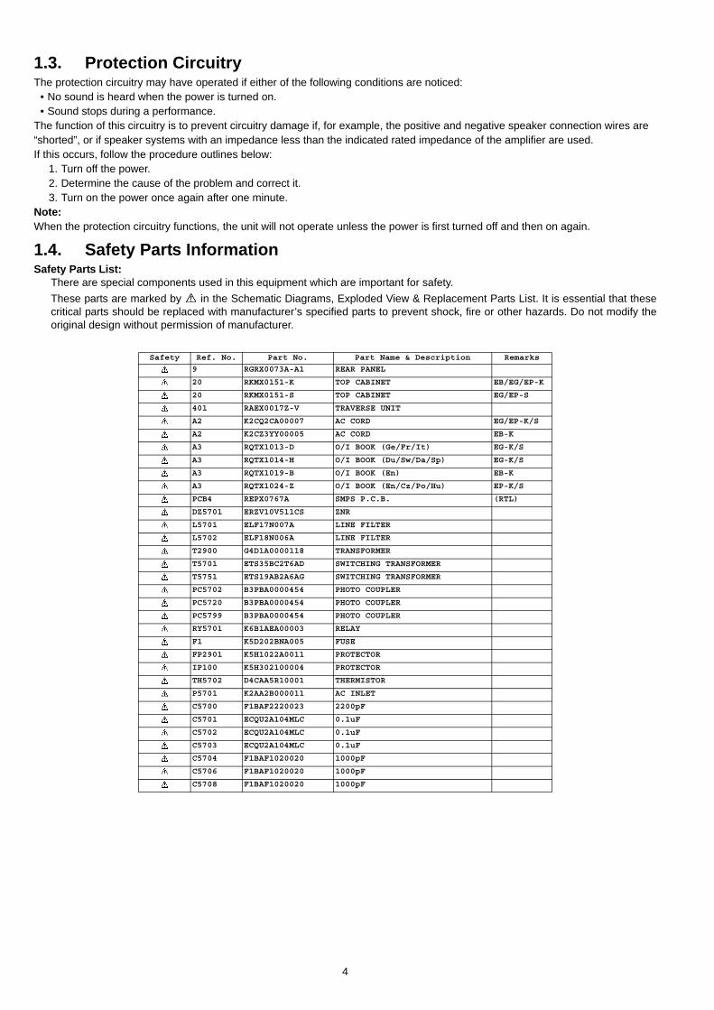
1.4. Safety Parts InformationSafety Parts List:
There are special components used in this equipment which are important for safety.
These parts are marked by in the Schematic Diagrams, Exploded View & Replacement Parts List. It is essential that thesecritical parts should be replaced with manufacturer’s specified parts to prevent shock, fire or other hazards. Do not modify theoriginal design without permission of manufacturer.
Safety Ref. No. Part No. Part Name & Description Remarks
9 RGRX0073A-A1 REAR PANEL
20 RKMX0151-K TOP CABINET EB/EG/EP-K
20 RKMX0151-S TOP CABINET EG/EP-S
401 RAEX0017Z-V TRAVERSE UNIT
A2 K2CQ2CA00007 AC CORD EG/EP-K/S
A2 K2CZ3YY00005 AC CORD EB-K
A3 RQTX1013-D O/I BOOK (Ge/Fr/It) EG-K/S
A3 RQTX1014-H O/I BOOK (Du/Sw/Da/Sp) EG-K/S
A3 RQTX1019-B O/I BOOK (En) EB-K
A3 RQTX1024-Z O/I BOOK (En/Cz/Po/Hu) EP-K/S
PCB4 REPX0767A SMPS P.C.B. (RTL)
DZ5701 ERZV10V511CS ZNR
L5701 ELF17N007A LINE FILTER
L5702 ELF18N006A LINE FILTER
T2900 G4D1A0000118 TRANSFORMER
T5701 ETS35BC2T6AD SWITCHING TRANSFORMER
T5751 ETS19AB2A6AG SWITCHING TRANSFORMER
PC5702 B3PBA0000454 PHOTO COUPLER
PC5720 B3PBA0000454 PHOTO COUPLER
PC5799 B3PBA0000454 PHOTO COUPLER
RY5701 K6B1AEA00003 RELAY
F1 K5D202BNA005 FUSE
FP2901 K5H1022A0011 PROTECTOR
IP100 K5H302100004 PROTECTOR
TH5702 D4CAA5R10001 THERMISTOR
P5701 K2AA2B000011 AC INLET
C5700 F1BAF2220023 2200pF
C5701 ECQU2A104MLC 0.1uF
C5702 ECQU2A104MLC 0.1uF
C5703 ECQU2A104MLC 0.1uF
C5704 F1BAF1020020 1000pF
C5706 F1BAF1020020 1000pF
C5708 F1BAF1020020 1000pF
4
1.5. Caution for AC Cord (For EB only)
5
2 Warning2.1. Prevention of Electrostatic Discharge (ESD) to Electrostatic Sensitive
(ES) DevicesSome semiconductor (solid state) devices can be damaged easily by static electricity. Such components commonly are called Elec-trostatically Sensitive (ES) Devices. Examples of typical ES devices are integrated circuits and some field-effect transistors andsemiconductor “chip” components. The following techniques should be used to help reduce the incidence of component damagecaused by electrostatic discharge (ESD).
1. Immediately before handling any semiconductor component or semiconductor-equipped assembly, drain off any ESD on yourbody by touching a known earth ground. Alternatively, obtain and wear a commercially available discharging ESD wrist strap,which should be removed for potential shock reasons prior to applying power to the unit under test.
2. After removing an electrical assembly equipped with ES devices, place the assembly on a conductive surface such as alumi-num foil, to prevent electrostatic charge build up or exposure of the assembly.
3. Use only a grounded-tip soldering iron to solder or unsolder ES devices.4. Use only an anti-static solder removal device. Some solder removal devices not classified as “anti-static (ESD protected)” can
generate electrical charge sufficient to damage ES devices.5. Do not use freon-propelled chemicals. These can generate electrical charges sufficient to damage ES devices.6. Do not remove a replacement ES device from its protective package until immediately before you are ready to install it. (Most
replacement ES devices are packaged with leads electrically shorted together by conductive foam, aluminum foil or compara-ble conductive material).
7. Immediately before removing the protective material from the leads of a replacement ES device, touch the protective materialto the chassis or circuit assembly into which the device will be installed.Caution:
Be sure no power is applied to the chassis or circuit, and observe all other safety precautions.8. Minimize bodily motions when handling unpackaged replacement ES devices. (Otherwise harmless motion such as the
brushing together of your clothes fabric or the lifting of your foot from a carpeted floor can generate static electricity (ESD) suf-
ficient to damage an ES device).
6
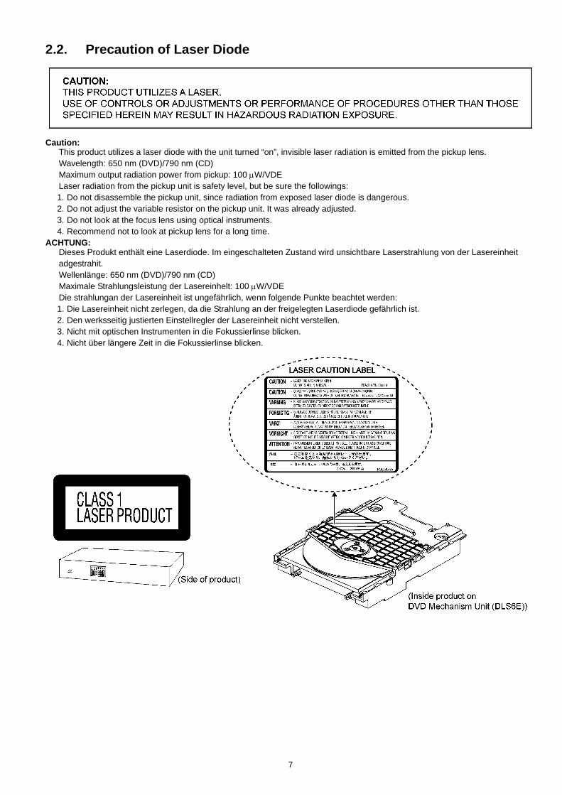
2.2. Precaution of Laser Diode
Caution:This product utilizes a laser diode with the unit turned “on”, invisible laser radiation is emitted from the pickup lens.Wavelength: 650 nm (DVD)/790 nm (CD)Maximum output radiation power from pickup: 100 µW/VDELaser radiation from the pickup unit is safety level, but be sure the followings: 1. Do not disassemble the pickup unit, since radiation from exposed laser diode is dangerous. 2. Do not adjust the variable resistor on the pickup unit. It was already adjusted.3. Do not look at the focus lens using optical instruments.4. Recommend not to look at pickup lens for a long time.
ACHTUNG:Dieses Produkt enthält eine Laserdiode. Im eingeschalteten Zustand wird unsichtbare Laserstrahlung von der Lasereinheitadgestrahit.Wellenlänge: 650 nm (DVD)/790 nm (CD)Maximale Strahlungsleistung der Lasereinhelt: 100 µW/VDEDie strahlungan der Lasereinheit ist ungefährlich, wenn folgende Punkte beachtet werden: 1. Die Lasereinheit nicht zerlegen, da die Strahlung an der freigelegten Laserdiode gefährlich ist. 2. Den werksseitig justierten Einstellregler der Lasereinheit nicht verstellen.3. Nicht mit optischen Instrumenten in die Fokussierlinse blicken.4. Nicht über längere Zeit in die Fokussierlinse blicken.
7
2.3. Service caution based on Legal restrictions
2.3.1. General description about Lead Free Solder (PbF)The lead free solder has been used in the mounting process of all electrical components on the printed circuit boards used for thisequipment in considering the globally environmental conservation.
The normal solder is the alloy of tin (Sn) and lead (Pb). On the other hand, the lead free solder is the alloy mainly consists of tin(Sn), silver (Ag) and Copper (Cu), and the melting point of the lead free solder is higher approx.30 degrees C (86°F) more than thatof the normal solder.
Definition of PCB Lead Free Solder being used
Service caution for repair work using Lead Free Solder (PbF)• The lead free solder has to be used when repairing the equipment for which the lead free solder is used.
(Definition: The letter of “PbF” is printed on the PCB using the lead free solder.)• To put lead free solder, it should be well molten and mixed with the original lead free solder.• Remove the remaining lead free solder on the PCB cleanly for soldering of the new IC.• Since the melting point of the lead free solder is higher than that of the normal lead solder, it takes the longer time to melt the
lead free solder.• Use the soldering iron (more than 70W) equipped with the temperature control after setting the temperature at 350±30 degrees
C (662±86°F).Recommended Lead Free Solder (Service Parts Route.)
• The following 3 types of lead free solder are available through the service parts route.RFKZ03D01K-----------(0.3mm 100g Reel)RFKZ06D01K-----------(0.6mm 100g Reel)RFKZ10D01K-----------(1.0mm 100g Reel)
Note* Ingredient: tin (Sn), 96.5%, silver (Ag) 3.0%, Copper (Cu) 0.5%, Cobalt (Co) / Germanium (Ge) 0.1 to 0.3%
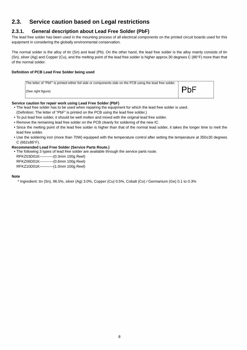
The letter of “PbF” is printed either foil side or components side on the PCB using the lead free solder. (See right figure)
8
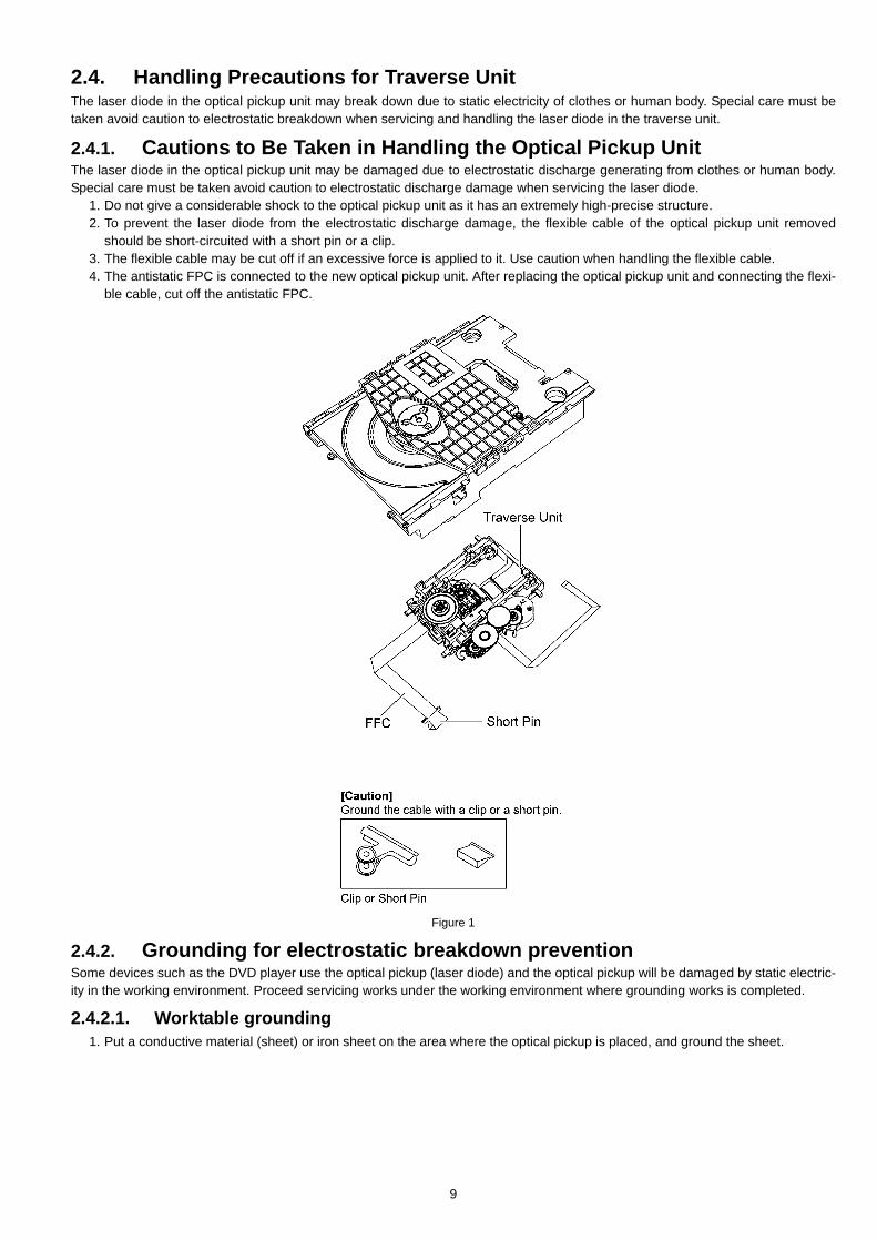
2.4. Handling Precautions for Traverse UnitThe laser diode in the optical pickup unit may break down due to static electricity of clothes or human body. Special care must betaken avoid caution to electrostatic breakdown when servicing and handling the laser diode in the traverse unit.
2.4.1. Cautions to Be Taken in Handling the Optical Pickup UnitThe laser diode in the optical pickup unit may be damaged due to electrostatic discharge generating from clothes or human body.Special care must be taken avoid caution to electrostatic discharge damage when servicing the laser diode.
1. Do not give a considerable shock to the optical pickup unit as it has an extremely high-precise structure.2. To prevent the laser diode from the electrostatic discharge damage, the flexible cable of the optical pickup unit removed
should be short-circuited with a short pin or a clip.3. The flexible cable may be cut off if an excessive force is applied to it. Use caution when handling the flexible cable.4. The antistatic FPC is connected to the new optical pickup unit. After replacing the optical pickup unit and connecting the flexi-
ble cable, cut off the antistatic FPC.
Figure 1
2.4.2. Grounding for electrostatic breakdown preventionSome devices such as the DVD player use the optical pickup (laser diode) and the optical pickup will be damaged by static electric-ity in the working environment. Proceed servicing works under the working environment where grounding works is completed.
2.4.2.1. Worktable grounding1. Put a conductive material (sheet) or iron sheet on the area where the optical pickup is placed, and ground the sheet.
9
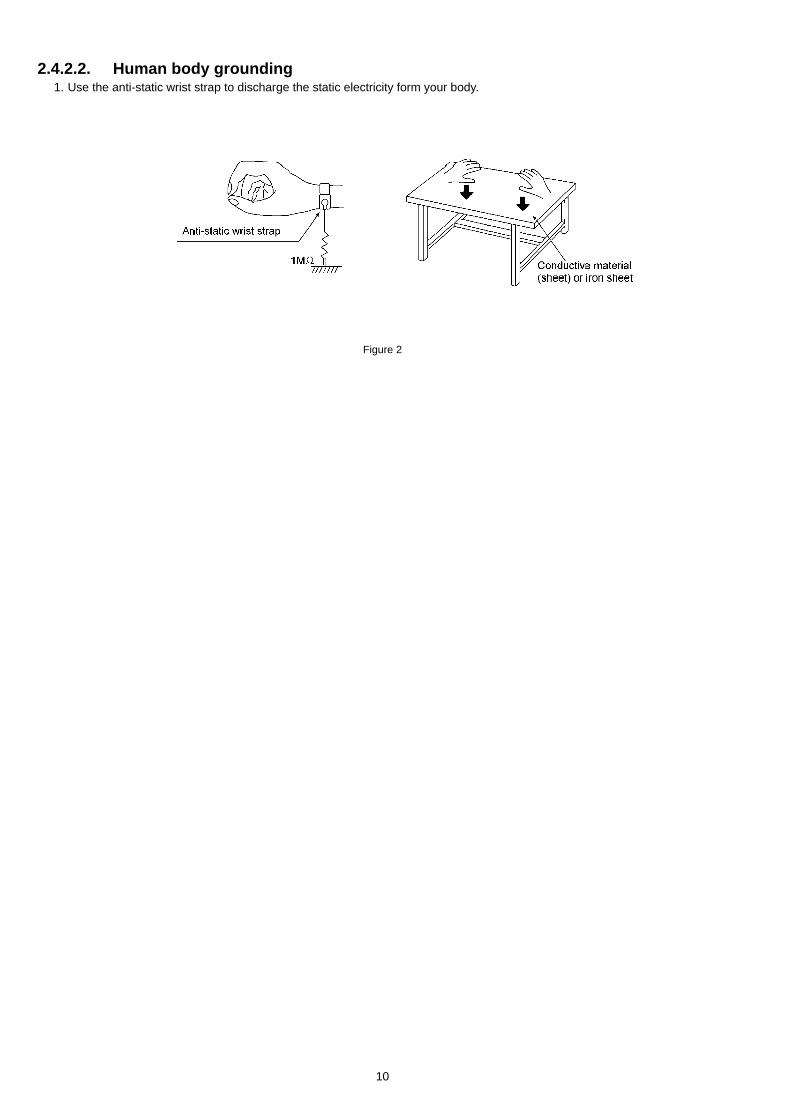
2.4.2.2. Human body grounding1. Use the anti-static wrist strap to discharge the static electricity form your body.
Figure 2
10
3 Service Navigation3.1. Service InformationThis service manual contains technical information which will allow service personnel’s to understand and service this model.Please place orders using the parts list and not the drawing reference numbers.
If the circuit is changed or modified, this information will be followed by supplement service manual to be filed with original servicemanual.
• DVD Mechanism Unit (DLS6E):
1) This model uses DVD Mechanism Unit (DLS6E).
• Printed Circuit boards:
1) The following category are supplied as an assembled module. • DVD Module P.C.B. (RFKBX0762A)
• Micro-processor & EEPROM IC:
1) The following components are supplied as an assembled part. • Micro-processor IC, IC200 (RFKWMPT70EGK) • EEPROM IC, IC201 (RFKWEPT70EGK)
11
4 Specifications
Main unit SA-PT70EB/EG/EPGENERAL
Power supply: AC 220 V to 240 V, 50 HzPower consumption: This unit 47 WPower consumption in standby mode:
approx. 0.48 W
Dimensions (W×H×D): 360 mm×58 mm×239 mmMass: This unit 2 kgOperating temperature range: 0 °C to +40 °COperating humidity range: 35 % to 80 % RH
(no condensation)AMPLIFIER SECTION
RMS Output Power: Dolby Digital ModeFront Ch:
55 W per channel (5 Ω), 1 kHz, 10% THDSurround Ch:
55 W per channel (5 Ω), 1 kHz, 10% THDCenter Ch:
55 W per channel (5 Ω), 1 kHz, 10% THDSubwoofer Ch:
55 W per channel (5 Ω), 100 Hz, 10% THDTotal RMS Dolby Digital mode power:
330 WFM TUNER, TERMINALS SECTION
Preset Memory: FM 30 stationsFrequency Modulation (FM)
Frequency range:87.50 MHz-108.00 MHz (50-kHz step)
Antenna terminals: 75 Ω (unbalanced)Music Port (Front)
Sensitivity100mV, 6.8 kΩ
TerminalStereo, 3.5 mm jack
DISC SECTIONDiscs played (8 cm or 12 cm):
(1) DVD (DVD-Video, DivX*5, 6)(2) DVD-R (DVD-Video, DVD-VR, MP3*2, 5, JPEG*4, 5, MPEG4*5,
7, DivX*5, 6)(3) DVD-R DL (DVD-Video, DVD-VR, DivX*5, 6)(4) DVD-RW (DVD-Video, DVD-VR, MP3*2, 5, JPEG*4, 5,
MPEG4*5, 7, DivX*5, 6)(5) +R/+RW (Video)(6) +R DL (Video)(7) CD, CD-R/RW (CD-DA, Video CD, SVCD*1, MP3*2, 5, WMA*3,
5, JPEG*4, 5, MPEG4*5, 7, DivX*5, 6)*1 Conforming to IEC62107
*2 MPEG-1 Layer 3, MPEG-2 Layer 3
*3 Windows Media Audio Ver.9.0 L3
Not compatible with Multiple Bit Rate (MBR)*4 Exif Ver 2.1 JPEG Baseline files
Picture resolution: between 160 x 120 and 6144 x 4096 pix-els (Sub sampling is 4:0:0, 4:2:0, 4:2:2 or 4:4:4). Extremely long and narrow pictures may not be displayed.
*5 The total combined maximum number of recognizable audio, picture and video contents and groups: 4000 audio, picture and video contents and 255 groups. (Excluding Root Folder)
*6 Plays DivX® video.*7 MPEG4 data recorded with the Panasonic SD multi cameras
or DVD video recorders.Conforming to SD VIDEO specifications (ASF standard)/
MPEG4 (Simple Profile) video system/G.726 audio system.
Pick upWavelength (DVD/CD): 650/790 nmLaser power (DVD/CD): CLASS 1M/CLASS 1M
Audio output (Disc)Number of channels: 5.1 ch (FL, FR, C, SL, SR, SW)
VIDEO SECTIONVideo system: PAL625/50, PAL525/60, NTSCComposite video output
Output level: 1 Vp-p (75 Ω)Terminal: Scart jack (1 system)
Component video outputR output level: 0.7 Vp-p (75 Ω)G output level: 0.7 Vp-p (75 Ω)B output level: 0.7 Vp-p (75 Ω)Terminal: Scart jack (1 system)
S-video outputY output level: 1 Vp-p (75 Ω)C output level: PAL; 0.3 Vp-p (75 Ω)
NTSC; 0.286 Vp-p (75 Ω)Terminal: Scart jack (1 system)
HDMI AV outputTerminal: 19-pin type A connector
HDAVI Control:This unit supports “HDAVI Control 4” function.
Note:1. Specifications are subject to change without notice.
Mass and dimensions are approximate.2. Total harmonic distortion is measured by the digital spectrum
analyzer.Solder:
This model uses lead free solder (PbF).
Refer to their respective original service manuals for *1.
12
13
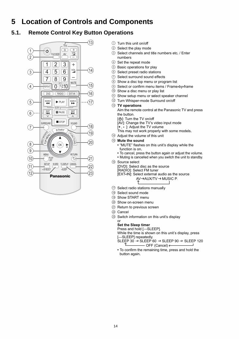
5 Location of Controls and Components5.1. Remote Control Key Button Operations
14
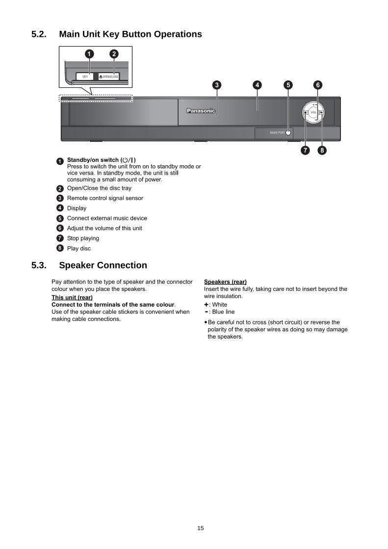
5.2. Main Unit Key Button Operations
5.3. Speaker Connection
15
5.4. Using the VIERA Link “HDAVI Control™”
16
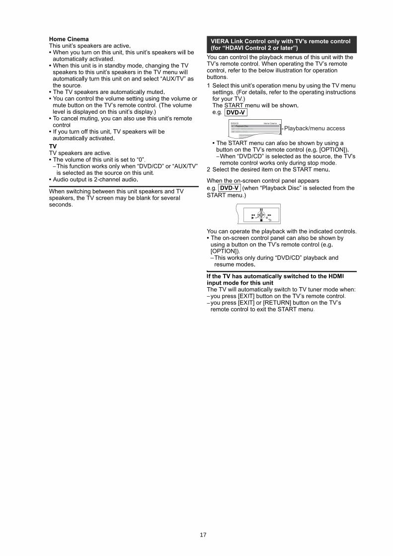
17
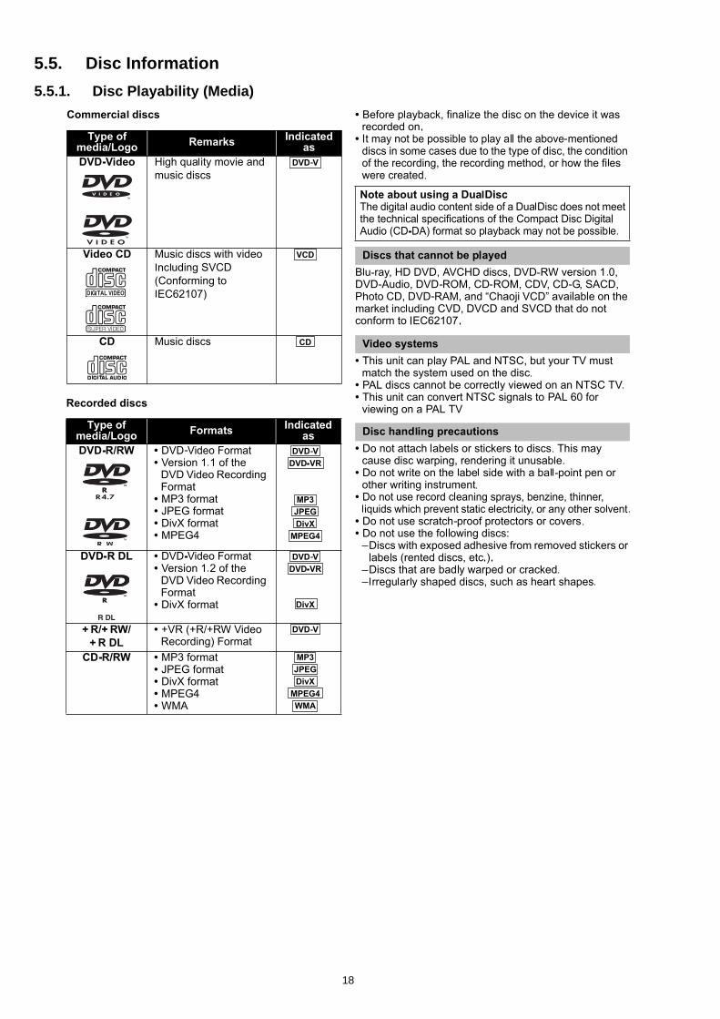
5.5. Disc Information
5.5.1. Disc Playability (Media)
18
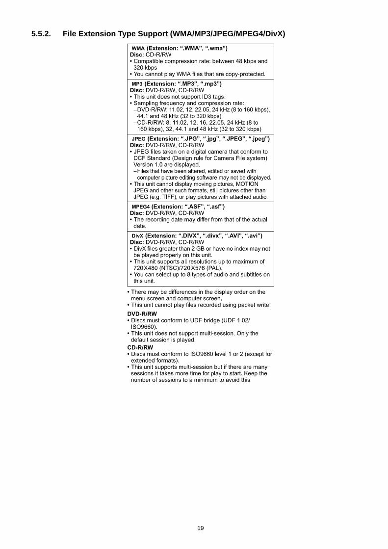
5.5.2. File Extension Type Support (WMA/MP3/JPEG/MPEG4/DivX)
19
6 Self-Diagnosis and Special Mode Setting6.1. Cold-StartHere is the procedure to carry out cold-start or initialize to shipping mode.
1. Unplug AC power cord2. Press & hold [POWER] button3. Plug AC power cord while [POWER] button being pressed
FL Display will show “_ _ _ _ _ _ _ _”4. Release [POWER] button
6.2. Service Mode TableBy pressing various button combinations on the main unit and remote control unit, you can activate the various service modes forchecking.Special Note:
• Due to the limitations of the no. characters that can be shown on the FL Display, the “FL Display” button on the remote controlunit can be used to show the two display pages. (Display 1 / Display 2).
• Refer to Section 5.1 for the section on “Remote Control Key Buttons Operations”.
20
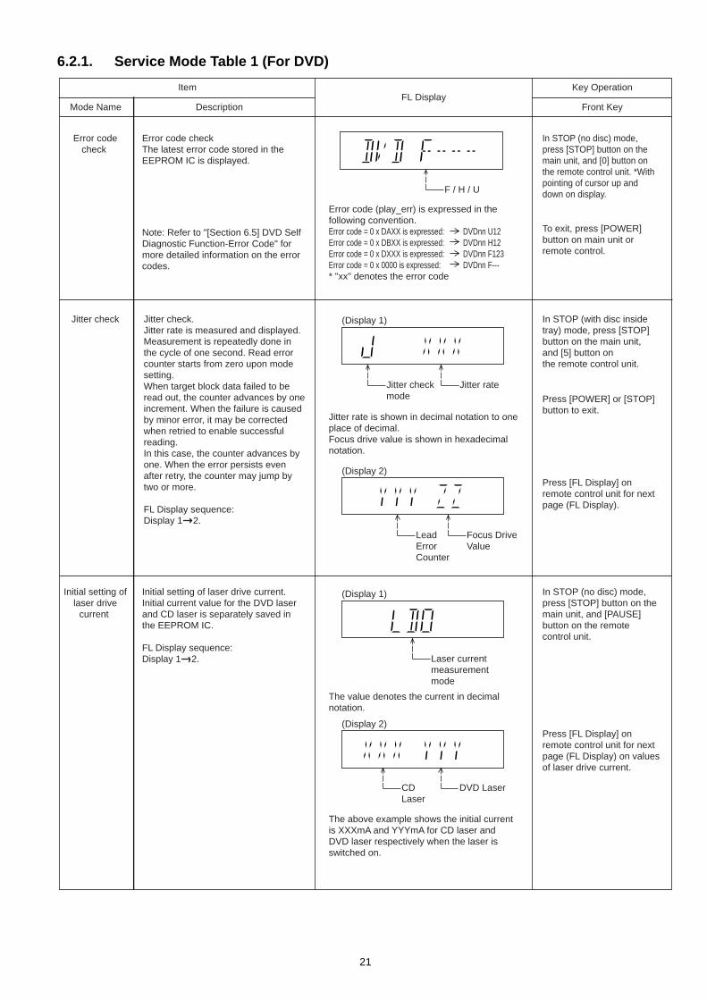
6.2.1. Service Mode Table 1 (For DVD)
Initial setting of
laser drive
current
Jitter check Jitter check.
Jitter rate is measured and displayed.
Measurement is repeatedly done in
the cycle of one second. Read error
counter starts from zero upon mode
setting.
When target block data failed to be
read out, the counter advances by one
increment. When the failure is caused
by minor error, it may be corrected
when retried to enable successful
reading.
In this case, the counter advances by
one. When the error persists even
after retry, the counter may jump by
two or more.
FL Display sequence:
Display 1 2.
Jitter rate is shown in decimal notation to one
place of decimal.
Focus drive value is shown in hexadecimal
notation.
(Display 1)
Jitter rateJitter check
mode
(Display 2)
Lead
Error
Counter
Focus Drive
Value
Press [POWER] or [STOP]
button to exit.
In STOP (with disc inside
tray) mode, press [STOP]
button on the main unit,
and [5] button on
the remote control unit.
Press [FL Display] on
remote control unit for next
page (FL Display).
Error code
check
Error code check
The latest error code stored in the
EEPROM IC is displayed.
Note: Refer to "[Section 6.5] DVD Self
Diagnostic Function-Error Code" for
more detailed information on the error
codes.
Error code (play_err) is expressed in the
following convention.
Error code = 0 x DAXX is expressed: DVDnn U12
Error code = 0 x DBXX is expressed: DVDnn H12
Error code = 0 x DXXX is expressed: DVDnn F123
Error code = 0 x 0000 is expressed: DVDnn F---
* "xx" denotes the error code
F / H / U
To exit, press [POWER]
button on main unit or
remote control.
In STOP (no disc) mode,
press [STOP] button on the
main unit, and [0] button on
the remote control unit. *With
pointing of cursor up and
down on display.
Press [FL Display] on
remote control unit for next
page (FL Display) on values
of laser drive current.
In STOP (no disc) mode,
press [STOP] button on the
main unit, and [PAUSE]
button on the remote
control unit.
Initial setting of laser drive current.
Initial current value for the DVD laser
and CD laser is separately saved in
the EEPROM IC.
FL Display sequence:
Display 1 2.
The value denotes the current in decimal
notation.
The above example shows the initial current
is XXXmA and YYYmA for CD laser and
DVD laser respectively when the laser is
switched on.
(Display 1)
Laser current
measurement
mode
(Display 2)
CD
Laser
DVD Laser
FL DisplayKey Operation
Front Key
Item
DescriptionMode Name
21
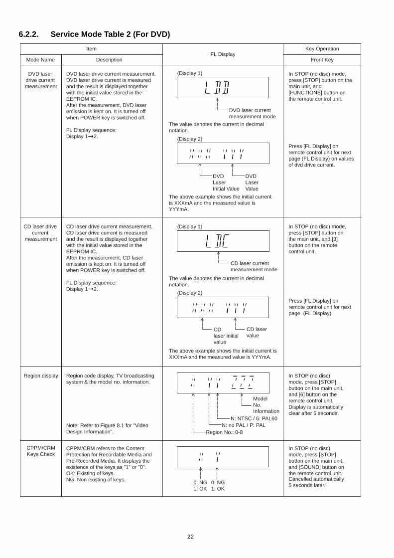
6.2.2. Service Mode Table 2 (For DVD)
FL DisplayKey Operation
Front Key
Item
DescriptionMode Name
CD laser drive
current
measurement
Press [FL Display] on
remote control unit for next
page. (FL Display)
In STOP (no disc) mode,
press [STOP] button on
the main unit, and [3]
button on the remote
control unit.
The value denotes the current in decimal
notation.
The above example shows the initial current is
XXXmA and the measured value is YYYmA.
DVD laser
drive current
measurement
CD laser current
measurement mode
(Display 1)
CD
laser initial
value
CD laser
value
(Display 2)
Press [FL Display] on
remote control unit for next
page (FL Display) on values
of dvd drive current.
In STOP (no disc) mode,
press [STOP] button on the
main unit, and
[FUNCTIONS] button on
the remote control unit.
The value denotes the current in decimal
notation.
The above example shows the initial current
is XXXmA and the measured value is
YYYmA.
DVD laser current
measurement mode
(Display 1)
DVD
Laser
Initial Value
DVD
Laser
Value
(Display 2)
DVD laser drive current measurement.
DVD laser drive current is measured
and the result is displayed together
with the initial value stored in the
EEPROM IC.
After the measurement, DVD laser
emission is kept on. It is turned off
when POWER key is switched off.
FL Display sequence:
Display 1 2.
CD laser drive current measurement.
CD laser drive current is measured
and the result is displayed together
with the initial value stored in the
EEPROM IC.
After the measurement, CD laser
emission is kept on. It is turned off
when POWER key is switched off.
FL Display sequence:
Display 1 2.
Region code display, TV broadcasting
system & the model no. information.
Note: Refer to Figure 8.1 for "Video
Design Information".
Region display
Display is automatically
clear after 5 seconds.
In STOP (no disc)
mode, press [STOP]
button on the main unit,
and [6] button on the
remote control unit.
N: no PAL / P: PAL
Model
No.
Information
N: NTSC / 6: PAL60
Region No.: 0-8
CPPM/CRM
Keys Check
Cancelled automatically
5 seconds later.
In STOP (no disc)
mode, press [STOP]
button on the main unit,
and [SOUND] button on
the remote control unit.
0: NG
1: OK
0: NG
1: OK
CPPM/CRM refers to the Content
Protection for Recordable Media and
Pre-Recorded Media. It displays the
existence of the keys as "1" or "0".
OK: Existing of keys.
NG: Non existing of keys.
22
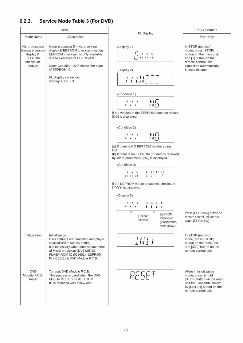
6.2.3. Service Mode Table 3 (For DVD)
FL DisplayKey Operation
Front Key
Item
DescriptionMode Name
Initialization
Micro-processor
firmware version
display &
EEPROM
checksum
display.
DVD
Module P.C.B.
Reset
Initialization.
User settings are cancelled and player
is initialized to factory setting.
It is necessary when after replacement
of Micro-processor (DV5 LSI) IC,
FLASH ROM IC (IC8651), EEPROM
IC (IC8611) & DVD Module P.C.B.
Micro-processor firmware version
display & EEPROM checksum display.
EEPROM checksum is only available
due to existence of EEPROM IC.
Note: Condition 1/2/3 shows the state
of EEPROM IC.
FL Display sequence:
Display 1 2 3.
To reset DVD Module P.C.B.
This process is used when the DVD
Module P.C.B. or FLASH ROM
IC is replaced with a new one.
In STOP (no disc)
mode, press [STOP]
button on the main unit,
and [ 10] button on the
remote control unit.
Cancelled automatically
5 seconds later.
In STOP (no disc)
mode, press [STOP]
button on the main unit,
and [7] button on the
remote control unit.
Press [FL Display] button on
remote control unit for next
page. (FL Display)
While in initialization
mode, press & hold
[STOP] button on the main
unit for 3 seconds, follow
by [ENTER] button on the
remote control unit.
(Display 2)
If the version of the EEPROM does not match,
[NG] is displayed.
(Condition 1)
(a) If there is NO EEPROM header string
OR
(b) If there is no EEPROM (no data is received
by Micro-processor), [NO] is displayed.
(Condition 2)
Opecon
Version
EEPROM
Checksum
(If applicable,
refer below.)
(Display 3)
(Display 1)
(Condition 3)
If the EEPROM version matches, checksum
[YYYY] is displayed.
23
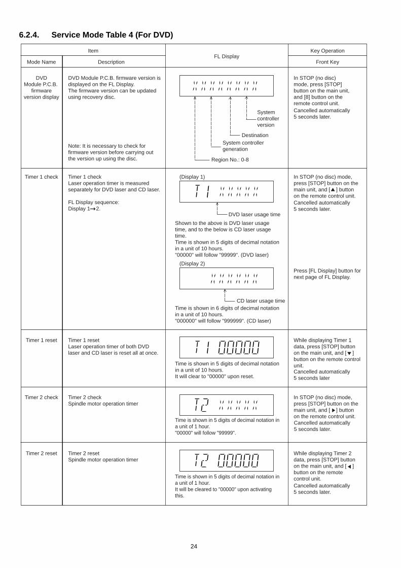
6.2.4. Service Mode Table 4 (For DVD)
FL DisplayKey Operation
Front Key
Item
DescriptionMode Name
DVD
Module P.C.B.
firmware
version display
Cancelled automatically
5 seconds later.
In STOP (no disc)
mode, press [STOP]
button on the main unit,
and [8] button on the
remote control unit.
DVD Module P.C.B. firmware version is
displayed on the FL Display.
The firmware version can be updated
using recovery disc.
Note: It is necessary to check for
firmware version before carrying out
the version up using the disc.
Destination
System
controller
version
System controller
generation
Region No.: 0-8
Timer 1 check
DVD laser usage time
(Display 1)
Shown to the above is DVD laser usage
time, and to the below is CD laser usage
time.
Time is shown in 5 digits of decimal notation
in a unit of 10 hours.
"00000" will follow "99999". (DVD laser)
(Display 2)
CD laser usage time
Time is shown in 6 digits of decimal notation
in a unit of 10 hours.
"000000" will follow "999999". (CD laser)
Press [FL Display] button for
next page of FL Display.
Cancelled automatically
5 seconds later.
In STOP (no disc) mode,
press [STOP] button on the
main unit, and [ ] button
on the remote control unit.
Timer 1 reset
Timer 2 check
Timer 2 reset
Timer 1 check
Laser operation timer is measured
separately for DVD laser and CD laser.
FL Display sequence:
Display 1 2.
Timer 1 reset
Laser operation timer of both DVD
laser and CD laser is reset all at once.
Timer 2 check
Spindle motor operation timer
Timer 2 reset
Spindle motor operation timer
Time is shown in 5 digits of decimal notation
in a unit of 10 hours.
It will clear to "00000" upon reset.
Time is shown in 5 digits of decimal notation in
a unit of 1 hour.
"00000" will follow "99999".
Time is shown in 5 digits of decimal notation in
a unit of 1 hour.
It will be cleared to "00000" upon activating
this.
Cancelled automatically
5 seconds later
While displaying Timer 1
data, press [STOP] button
on the main unit, and [ ]
button on the remote control
unit.
Cancelled automatically
5 seconds later.
In STOP (no disc) mode,
press [STOP] button on the
main unit, and [ ] button
on the remote control unit.
Cancelled automatically
5 seconds later.
While displaying Timer 2
data, press [STOP] button
on the main unit, and [ ]
button on the remote
control unit.
24
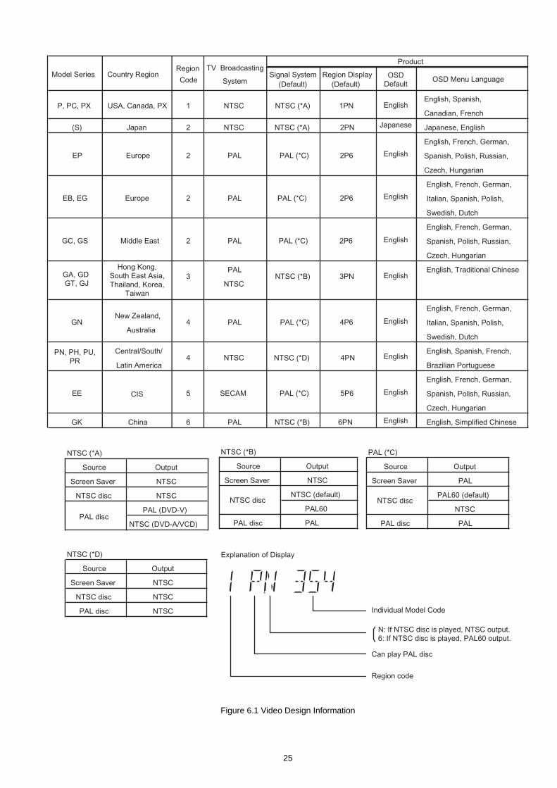
Figure 6.1 Video Design Information
English, Spanish,
Canadian, French
(S) Japanese, English
English, French, German,
Spanish, Polish, Russian,
Czech, Hungarian
English, French, German,
Italian, Spanish, Polish,
Swedish, Dutch
English, French, German,
Spanish, Polish, Russian,
Czech, Hungarian
GA, GD GT, GJ
English, Traditional Chinese
English, French, German,
Italian, Spanish, Polish,
Swedish, Dutch
English, Spanish, French,
Brazilian Portuguese
English, French, German,
Spanish, Polish, Russian,
Czech, Hungarian
GK English, Simplified Chinese
GN
EE
PN, PH, PU,PR
EP
P, PC, PX
GC, GS
EB, EG
NTSC (*B)
Source Output
Screen Saver NTSC
NTSC discNTSC (default)
PAL60
PAL disc PAL
NTSC (*A)
Source Output
Screen Saver NTSC
NTSC disc NTSC
PAL discPAL (DVD-V)
NTSC (DVD-A/VCD)
NTSC (*D)
Source Output
Screen Saver NTSC
NTSC disc NTSC
PAL disc NTSC
PAL (*C)
Source Output
Screen Saver PAL
NTSC discPAL60 (default)
NTSC
PAL disc PAL
Explanation of Display
Individual Model Code
Can play PAL disc
Region code
N: If NTSC disc is played, NTSC output.6: If NTSC disc is played, PAL60 output.
2
6
5
4
4
2
2
1
2
3
Region
Code
NTSC
PAL
NTSC
PAL
SECAM
NTSC
PAL
PAL
PAL
NTSC
PAL
TV Broadcasting
SystemSignal System
NTSC (*A)
NTSC (*D)
NTSC (*B)
PAL (*C)
PAL (*C)
PAL (*C)
PAL (*C)
PAL (*C)
NTSC (*A)
NTSC (*B)
(Default)
2PN
4PN
6PN
5P6
3PN
4P6
2P6
2P6
1PN
2P6
Region Display(Default)
Product
Model Series
Japan
Hong Kong,South East Asia,Thailand, Korea,
Taiwan
New Zealand,
Australia
Central/South/
Latin America
China
CIS
Europe
USA, Canada, PX
Europe
Middle East
Country RegionOSD Menu LanguageOSD
Default
English
English
English
English
English
English
English
English
English
Japanese
25
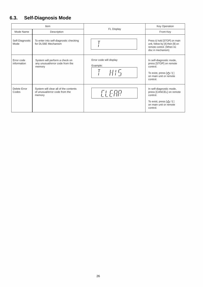
6.3. Self-Diagnosis Mode
Delete Error
Codes
Error code
information
System will perform a check on
any unusual/error code from the
memory
Error code will display
Example:
In self-diagnostic mode,
press [STOP] on remote
control.
To exist, press [ / ]
on main unit or remote
control.
Self-Diagnostic
Mode
To enter into self-diagnostic checking
for DLS6E Mechanism
Press & hold [STOP] on main
unit, follow by [4] then [9] on
remote control. (When no
disc in mechanism)
System will clear all of the contents
of unusual/error code from the
memory
FL DisplayKey Operation
Front Key
Item
DescriptionMode Name
In self-diagnostic mode,
press [CANCEL] on remote
control.
To exist, press [ / ]
on main unit or remote
control.
26
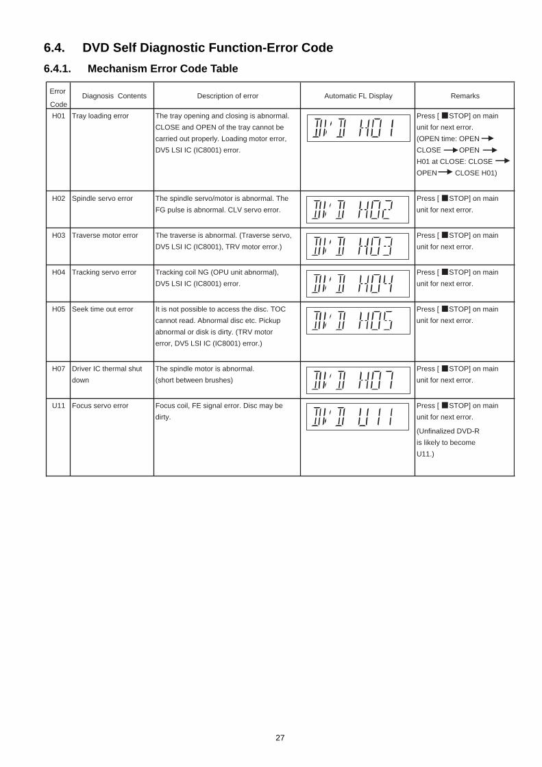
6.4. DVD Self Diagnostic Function-Error Code
6.4.1. Mechanism Error Code Table
Error
Code
H01 Tray loading error The tray opening and closing is abnormal. Press [ STOP] on main
CLOSE and OPEN of the tray cannot be unit for next error.
carried out properly. Loading motor error, (OPEN time: OPEN
DV5 LSI IC (IC8001) error. CLOSE OPEN
H01 at CLOSE: CLOSE
OPEN CLOSE H01)
H02 Spindle servo error The spindle servo/motor is abnormal. The Press [ STOP] on main
FG pulse is abnormal. CLV servo error. unit for next error.
H03 Traverse motor error The traverse is abnormal. (Traverse servo, Press [ STOP] on main
DV5 LSI IC (IC8001), TRV motor error.) unit for next error.
H04 Tracking servo error Tracking coil NG (OPU unit abnormal), Press [ STOP] on main
DV5 LSI IC (IC8001) error. unit for next error.
H05 Seek time out error It is not possible to access the disc. TOC Press [ STOP] on main
cannot read. Abnormal disc etc. Pickup unit for next error.
abnormal or disk is dirty. (TRV motor
error, DV5 LSI IC (IC8001) error.)
H07 Driver IC thermal shut The spindle motor is abnormal. Press [ STOP] on main
down (short between brushes) unit for next error.
U11 Focus servo error Focus coil, FE signal error. Disc may be Press [ STOP] on main
dirty. unit for next error.
(Unfinalized DVD-R
is likely to become
U11.)
Description of error Automatic FL Display RemarksDiagnosis Contents
27
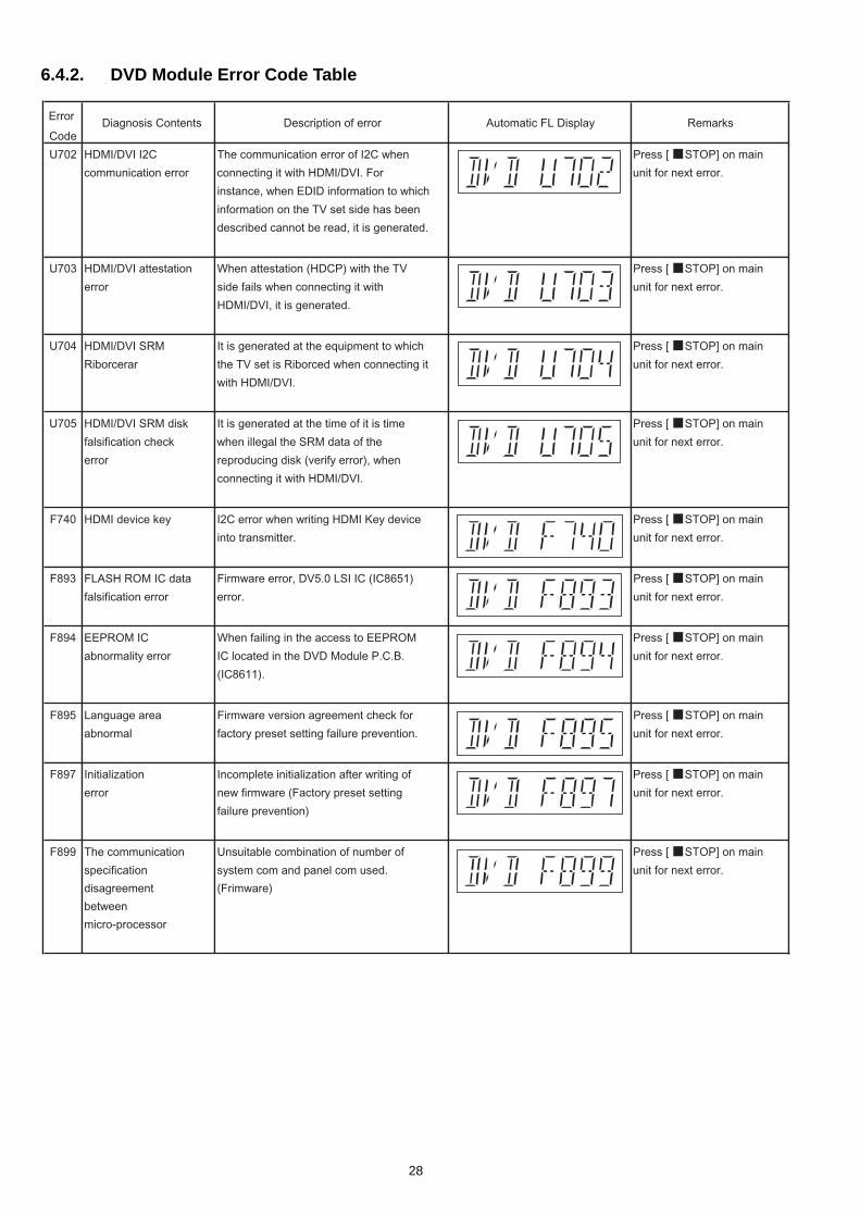
6.4.2. DVD Module Error Code Table
Error
Code
U702 HDMI/DVI I2C The communication error of I2C when Press [ STOP] on main
communication error connecting it with HDMI/DVI. For unit for next error.
instance, when EDID information to which
information on the TV set side has been
described cannot be read, it is generated.
U703 HDMI/DVI attestation When attestation (HDCP) with the TV Press [ STOP] on main
error side fails when connecting it with unit for next error.
HDMI/DVI, it is generated.
U704 HDMI/DVI SRM It is generated at the equipment to which Press [ STOP] on main
Riborcerar the TV set is Riborced when connecting it unit for next error.
with HDMI/DVI.
U705 HDMI/DVI SRM disk It is generated at the time of it is time Press [ STOP] on main
falsification check when illegal the SRM data of the unit for next error.
error reproducing disk (verify error), when
connecting it with HDMI/DVI.
F740 HDMI device key I2C error when writing HDMI Key device Press [ STOP] on main
into transmitter. unit for next error.
F893 FLASH ROM IC data Firmware error, DV5.0 LSI IC (IC8651) Press [ STOP] on main
falsification error error. unit for next error.
F894 EEPROM IC When failing in the access to EEPROM Press [ STOP] on main
abnormality error IC located in the DVD Module P.C.B. unit for next error.
(IC8611).
F895 Language area Firmware version agreement check for Press [ STOP] on main
abnormal factory preset setting failure prevention. unit for next error.
F897 Initialization Incomplete initialization after writing of Press [ STOP] on main
error new firmware (Factory preset setting unit for next error.
failure prevention)
F899 The communication Unsuitable combination of number of Press [ STOP] on main
specification system com and panel com used. unit for next error.
disagreement (Frimware)
between
micro-processor
Diagnosis Contents Description of error Automatic FL Display Remarks
28
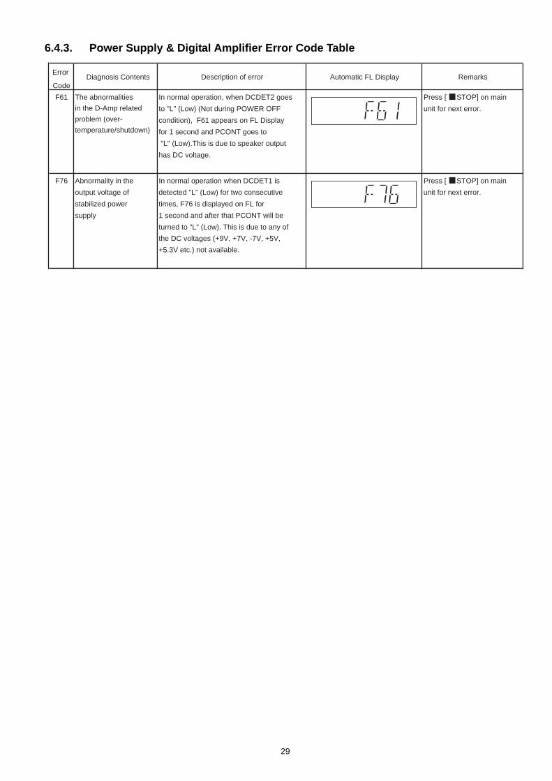
6.4.3. Power Supply & Digital Amplifier Error Code Table
Error
Code
F61 The abnormalities
in the D-Amp related
problem (over-
temperature/shutdown)
In normal operation, when DCDET2 goes Press [ STOP] on main
to "L" (Low) (Not during POWER OFF unit for next error.
condition), F61 appears on FL Display
for 1 second and PCONT goes to
"L" (Low).This is due to speaker output
has DC voltage.
F76 Abnormality in the In normal operation when DCDET1 is Press [ STOP] on main
output voltage of detected "L" (Low) for two consecutive unit for next error.
stabilized power times, F76 is displayed on FL for
supply 1 second and after that PCONT will be
turned to "L" (Low). This is due to any of
the DC voltages (+9V, +7V, -7V, +5V,
+5.3V etc.) not available.
Diagnosis Contents Description of error Automatic FL Display Remarks
29
6.5. Sales Demonstration Lock FunctionThis function prevents discs from being lost when the unit is used for sales demonstrations by disabling the disc eject function.“LOCKED” is displayed on the unit, and ordinary operation is disabled.
6.5.1. Setting• Prohibiting removal of disc
1. Select the DVD/CD function.2. At POWER ON condition, press and hold down the [ ] button and the [POWER] button on the main unit for at least three
seconds. (The message, “LOCKED” appears when the function is activated.)Note:
OPEN/CLOSE button is invalid and the main unit displays “LOCKED” while the lock function mode is entered.
• Prohibiting operation of selector and disc1. Select the DVD/CD function.2. At POWER ON condition, press and hold down the [ ] button and the [POWER] button on the main unit for at least three
seconds. (The message, “LOCKED” appears when the function is activated.)Note:
The following buttons are invalid and the main unit displays “LOCKED” while the lock function mode is entered.
6.5.2. CancellationThe lock can be cancelled by the same procedure as used in setting. (“UNLOCKED” is displayed on cancellation. Disconnecting thepower cable from power outlet does not cancel the lock.)
Main unit OPEN/CLOSE, , Remote con-
troller unitEXT-IN, REPEAT, RADIO, NUMERIC KEYS 0~9, , , , , , , , RETURN, FUNCTIONS,FL DISPLAY/SLEEP, MUTE
30
6.6. Firmware Version-Up Information
6.6.1. Process Flow (1/3)
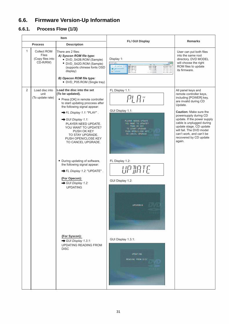
Collect ROM Files
(Copy files intoCD-R/RW)
Load disc intounit
(To update rate)
Load the disc into the set
(To be updated).
There are 2 files:A) Syscon ROM file type:
DVD_S42B.ROM (Sample)DVD_S42D.ROM (Sample)(supports chinese fonts OSDdisplay)
B) Opecon ROM file type:DVD_P05.ROM (Single tray)
Press [OK] in remote controllerto start updating proccess after the following signal appear:
During updating of software,the following signal appear:
All panel keys and remote controller keys,including [POWER] key,are invalid during CDUpdate.
Caution: Make sure the powersupply during CD update. If the power supply cable is unplugged during update stage, CD update will fail. The DVD model can’t work, and can’t be recovered by CD update again.
User can put both files into the same root directory. DVD MODEL will choose the right ROM files to update its firmware.
Display 1:
FL Display 1.1:
FL Display 1.2:
FL Display 1.1: "PLAY" .
FL Display 1.2: "UPDATE" .
GUI Display 1.1: PLAYER NEED UPDATE.YOU WANT TO UPDATE?
PUSH OK KEYTO STAY UPGRADE.
PUSH OPEN/CLOSE KEYTO CANCEL UPGRADE.
GUI Display 1.2: UPDATING
GUI Display 1.1:
GUI Display 1.2:
GUI Display 1.3.1:
FL/ GUI Display RemarksItem
DescriptionProcess
1
2
(For Opecon):
GUI Display 1.3.1: UPDATING READING FROMDISC
(For Syscon):
31
6.6.2. Process Flow (2/3)
FL/ GUI Display RemarksItem
DescriptionProcess
Check ROMversion type
Update not Necessary
If the ROM files has the same (latest) version or an older version than the product:
Update stop (product has the latest firmware)
FL Display 3: "NO NEED" .
GUI Display 3: THIS PLAYER DOES NOT
REQUIRE THE UPDATE
GUI Display 3:
FL Display 3: 2-2
Check CorrectROM file type
ROM files doesn’t fit to the
product type.
If the ROM files doesn’t fit for the product type, then CD update "STOP" and display as below:
Update stop (Wrong ROM Type)
FL Display 2:
FL Display 2: "NO PLAY" .
GUI Display 2 : THIS TYPE OF DISC CANNOTBE PLAYER. PLEASE INSERT
A DIFFERENT DISC.
GUI Display 2:
GUI Display 1.3.2:
2-1
GUI Display 1.3.2: UPDATING WRITING TOFLASHROM
32
6.6.3. Process Flow (3/3)
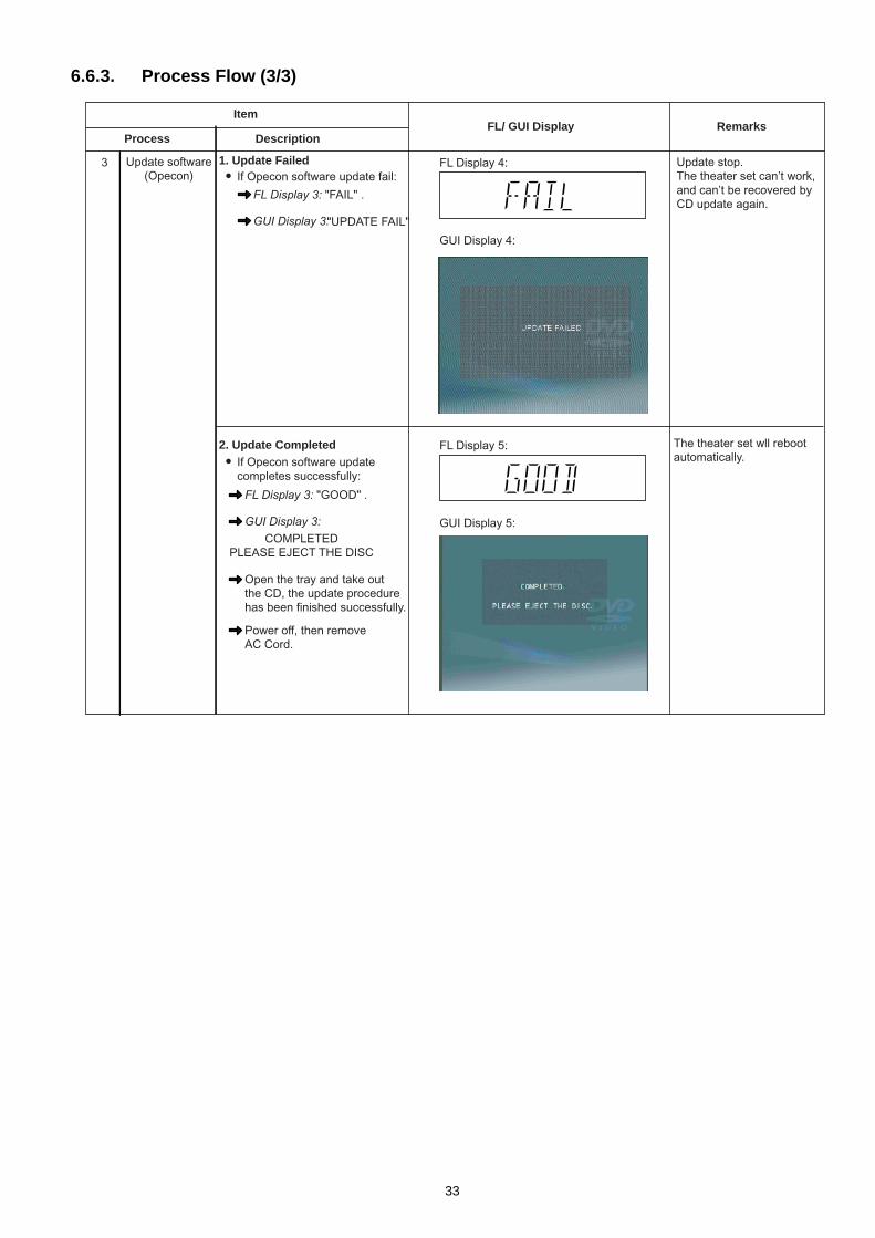
Update software(Opecon)
1. Update Failed
2. Update Completed
If Opecon software update fail:
If Opecon software update completes successfully:
Update stop.The theater set can’t work, and can’t be recovered by CD update again.
The theater set wll rebootautomatically.
FL Display 3: "FAIL" .
GUI Display 3: "UPDATE FAIL"
FL Display 3: "GOOD" .
Open the tray and take outthe CD, the update procedurehas been finished successfully.
Power off, then removeAC Cord.
GUI Display 3: COMPLETED
PLEASE EJECT THE DISC
GUI Display 4:
FL Display 4:
GUI Display 5:
FL Display 5:
3
FL/ GUI Display RemarksItem
DescriptionProcess
33
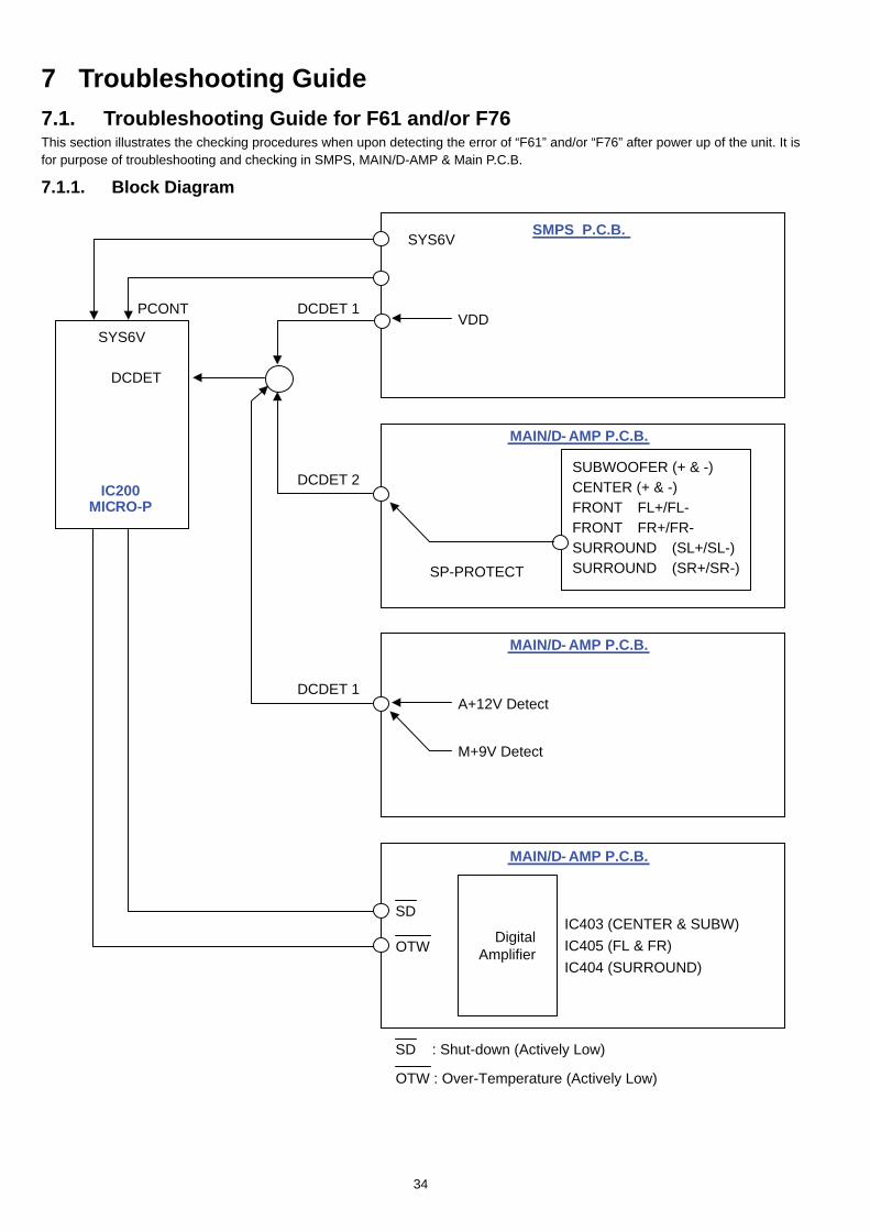
7 Troubleshooting Guide7.1. Troubleshooting Guide for F61 and/or F76This section illustrates the checking procedures when upon detecting the error of “F61” and/or “F76” after power up of the unit. It isfor purpose of troubleshooting and checking in SMPS, MAIN/D-AMP & Main P.C.B.
7.1.1. Block Diagram
SP-PROTECT
SUBWOOFER (+ & -)
Digital
Amplifier
IC403 (CENTER & SUBW)
IC405 (FL & FR)
IC404 (SURROUND)
CENTER (+ & -)
FRONT FL+/FL-
FRONT FR+/FR-
SURROUND (SL+/SL-)
SURROUND (SR+/SR-)
VDD
SYS6V
MAIN/D- AMP P.C.B.
MAIN/D- AMP P.C.B.
SMPS P.C.B.
MICRO-PIC200
DCDETPCONT 1
DCDET
SYS6V
DCDET 2
MAIN/D- AMP P.C.B.
DCDET 1A+12V Detect
SD
OTW
M+9V Detect
SD : Shut-down (Actively Low)
OTW : Over-Temperature (Actively Low)
34
7.1.2. Troubleshooting Guide
Symptom Checking items Possible Fault(s) Remarks
Unit cannot power up (No standby LED)
1) Check AC cord connection
2) Fuse, F1 3) AC inlet, P5701
1) Faulty AC cord (No Power) 2) Fuse, F1 blow (open circuit) 3) AC inlet, P5701 solder crack, dry-
joint etc 4) L5701 and/or L5702 open circuit 5) TH5702 faulty
SMPS P.C.B
Refer to Figure 1
SMPS P.C.B
Refer to Figure 1
Refer to Figure 2
Power on for a while then trigger “F61”
1) Check Speaker connections
2) Check pin 21 & pin 22 of IC200 (micro-p)
3) Check +VDD & feedback circuit
1) Speakers short-circuit (check individual channels)
2) Over-temperature 3) Shunt regulator, IC5801 faulty 4) Feedback circuit: PC5720, D5725
faulty 5) Main Transformer faulty, T5701
(Primary circuit) 6) Switching regulator, IC5701 faulty 7) Diode, D5701 faulty
Power on for a while and then trigger “F76”
1) Check VDD & SYS6V at pin 1,2,5 at H2016 of SMPS P.C.B.
2) Check voltage: –Vp, FL1 & FL2 at pin 15, 12 & 13 of H2016 (FL no display)
3) Check Pin 2 of Switching regulator, IC106 (For DVD + 5V & +3.3V)
4) Check E of Q107 (For M+9V)
1) Cable/Wire not connected properly between Main/D-Amp P.C.B & SMPS P.C.B or broken.
2) Main Transformer, T5701 short/open or broken.
3) Switching regulator, D5802 faulty. 4) Switching Transformer, T2900 faulty 5) L2915/L2916 Open circuit 6) L2910 Open circuit 7) FP2901 open circuit. 8) Switching regulator IC, IC106 faulty
(No DVD +5V/ +3.3V & SW5V) 9) IP100 faulty (open circuit) – No
+12V supply to Q107 (regulator circuit)
a) SMP P.C.B
Refer to
Figure 1
Refer to
Figure 2
b) Main / D-Amp P.C.B
No audio output to speaker 1) Check O/P of Digital Amplifier IC (Pin 28, 31, 36 & 39, 36)
2) Check I/P to Digital Amplifier IC (Pin 6, 8, 16, 18)
3) Check supply to Digital Amplifier IC (IC403, IC404, IC405) , VDD (Pin 21)
4) Check DAP IC I/P (Pin 28, 30, 31)
5) Check DAP IC, IC401 (Pin 40 to 52)
6) Check speaker connection
1) Digital Amplifier (IC403, IC404 or IC405) IC faulty (There is voltage supply & I/P but no O/P)
2) DAP IC, IC401 faulty (There is supply to DAP IC & I/P but no O/P)
3) No oscillating signal, X401 faulty
Main / D-Amp P.C.B
35
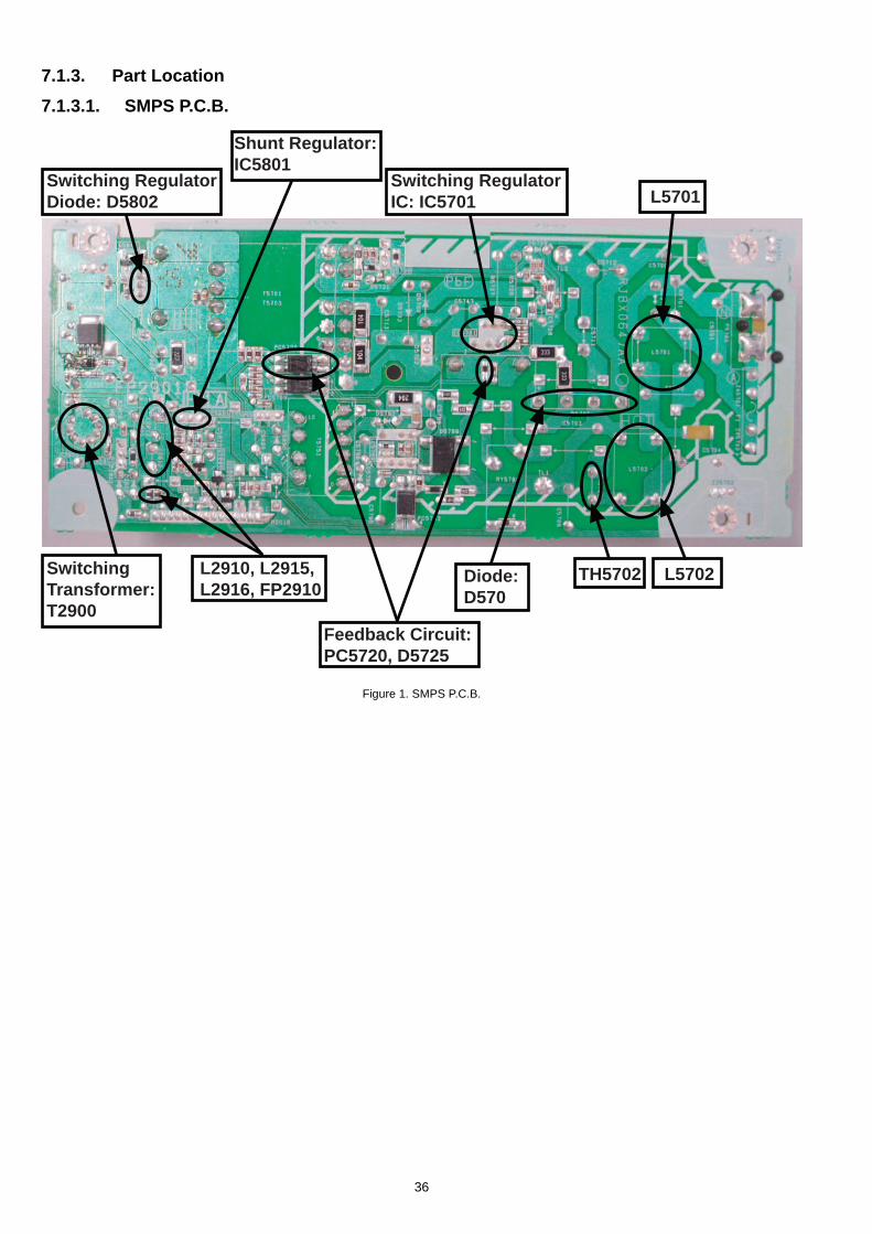
7.1.3. Part Location
7.1.3.1. SMPS P.C.B.
Figure 1. SMPS P.C.B.
Switching Regulator
Diode: D5802
Switching
Transformer:
T2900
L2910, L2915,
L2916, FP2910
Feedback Circuit:
PC5720, D5725
TH5702Diode:
D570
L5702
Shunt Regulator:
IC5801Switching Regulator
IC: IC5701 L5701
36
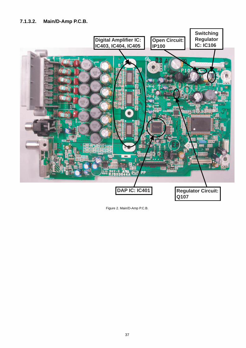
7.1.3.2. Main/D-Amp P.C.B.
Figure 2. Main/D-Amp P.C.B.
Digital Amplifier IC:
IC403, IC404, IC405
DAP IC: IC401 Regulator Circuit:
Q107
Switching
Regulator
IC: IC106Open Circuit:
IP100
37
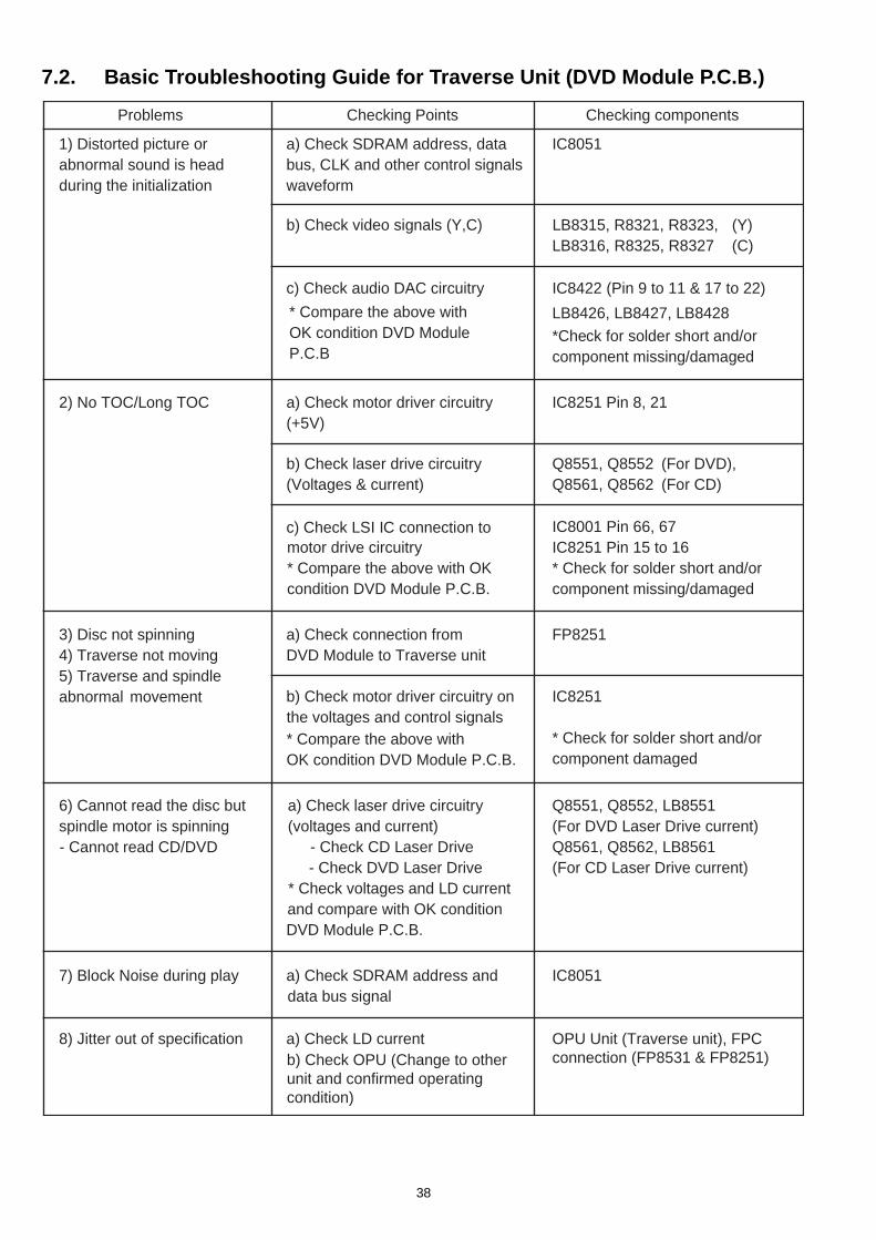
7.2. Basic Troubleshooting Guide for Traverse Unit (DVD Module P.C.B.)
Problems Checking Points Checking components
b) Check video signals (Y,C) LB8315, R8321, R8323,
LB8316,
(Y)
(C) R8325, R8327
a) Check SDRAM address, data
bus, CLK and other control signals
waveform
IC80511) Distorted picture or
abnormal sound is head
during the initialization
c) Check audio DAC circuitry
* Compare the above with
OK condition DVD Module
P.C.B
IC8422 (Pin 9 to 11 & 17 to 22)
LB8426, LB8427, LB8428
*Check for solder short and/or
component missing/damaged
b) Check laser drive circuitry
(Voltages & current)
Q8551, Q8552 (For DVD),
Q8561, Q8562 (For CD)
a) Check motor driver circuitry
(+5V)
IC8251 Pin 8, 212) No TOC/Long TOC
c) Check LSI IC connection to
motor drive circuitry
* Compare the above with OK
condition DVD Module P.C.B.
IC8001 Pin 66, 67
IC8251 Pin 15 to 16
* Check for solder short and/or
component missing/damaged
a) Check connection from
DVD Module to Traverse unit
FP82513) Disc not spinning
4) Traverse not moving
5) Traverse and spindle
abnormal movement b) Check motor driver circuitry on
the voltages and control signals
* Compare the above with
OK condition DVD Module P.C.B.
IC8251
* Check for solder short and/or
component damaged
6) Cannot read the disc but
spindle motor is spinning
- Cannot read CD/DVD
a) Check laser drive circuitry
(voltages and current)
- Check CD Laser Drive
- Check DVD Laser Drive
* Check voltages and LD current
and compare with OK condition
DVD Module P.C.B.
Q8551, Q8552, LB8551
(For DVD Laser Drive current)
Q8561, Q8562, LB8561
(For CD Laser Drive current)
7) Block Noise during play a) Check SDRAM address and
data bus signal
IC8051
8) Jitter out of specification a) Check LD current
b) Check OPU (Change to other
unit and confirmed operating
condition)
OPU Unit (Traverse unit), FPC
connection (FP8531 & FP8251)
38
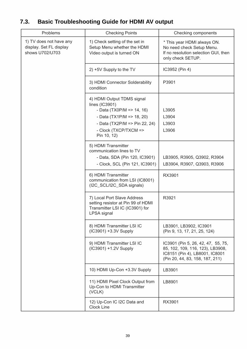
7.3. Basic Troubleshooting Guide for HDMI AV output
Problems Checking Points Checking components
1) Check setting of the set in Setup Menu whether the HDMI Video output is turned ON
* This year HDMI always ON. No need check Setup Menu. If no resolution selection GUI, then only check SETUP.
2) +5V Supply to the TV IC3952 (Pin 4)
3) HDMI Connector Solderability condition
P3901
4) HDMI Output TDMS signal lines (IC3901)
- Data (TX0P/M => 14, 16)
- Data (TX1P/M => 18, 20)
- Data (TX2P/M => Pin 22, 24)
- Clock (TXCP/TXCM =>Pin 10, 12)
L3905
L3904
L3903
L3906
- Data, SDA (Pin 120, IC3901)
- Clock, SCL (Pin 121, IC3901)
5) HDMI Transmittercommunication lines to TV
6) HDMI Transmittercommunication from LSI (IC8001)(I2C_SCL/I2C_SDA signals)
7) Local Port Slave Address setting resistor at Pin 99 of HDMITransmitter LSI IC (IC3901) forLPSA signal
8) HDMI Transmitter LSI IC(IC3901) +3.3V Supply
9) HDMI Transmitter LSI IC(IC3901) +1.2V Supply
10) HDMI Up-Con +3.3V Supply
12) Up-Con IC I2C Data andClock Line
LB3905, R3905, Q3902, R3904
LB3904, R3907, Q3903, R3906
RX3901
R3921
LB3901, LB3902, IC3901(Pin 9, 13, 17, 21, 25, 124)
IC3901 (Pin 5, 26, 42, 47, 55, 75,85, 102, 109, 116, 123), LB3908,IC8151 (Pin 4), LB8001, IC8001(Pin 20, 44, 83, 158, 187, 211)
1) TV does not have any display. Set FL display shows U702/U703
LB3901
11) HDMI Pixel Clock Output fromUp-Con to HDMI Transmitter(VCLK)
LB8901
RX3901
39
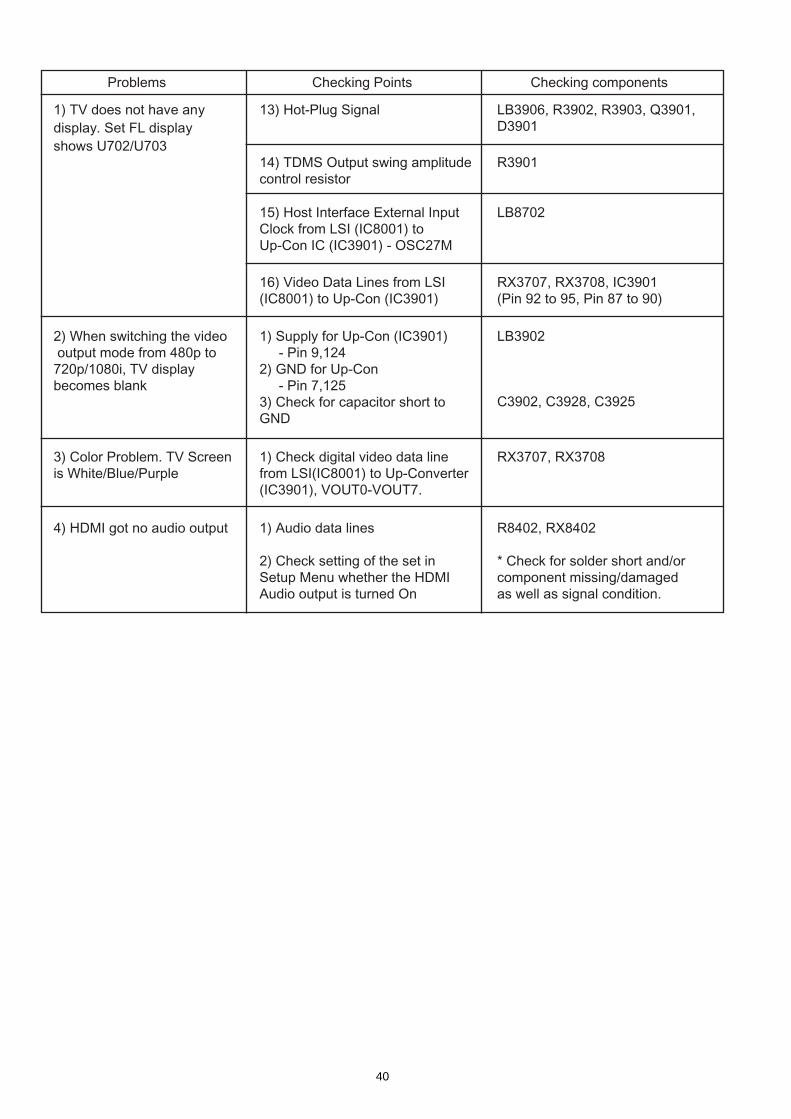
Problems Checking Points Checking components
13) Hot-Plug Signal
14) TDMS Output swing amplitudecontrol resistor
LB3906, R3902, R3903, Q3901,D3901
R3901
15) Host Interface External InputClock from LSI (IC8001) to Up-Con IC (IC3901) - OSC27M
LB8702
16) Video Data Lines from LSI(IC8001) to Up-Con (IC3901)
RX3707, RX3708, IC3901 (Pin 92 to 95, Pin 87 to 90)
1) Supply for Up-Con (IC3901) - Pin 9,1242) GND for Up-Con - Pin 7,1253) Check for capacitor short toGND
LB3902
1) Check digital video data linefrom LSI(IC8001) to Up-Converter(IC3901), VOUT0-VOUT7.
RX3707, RX3708
C3902, C3928, C3925
1) TV does not have any display. Set FL display shows U702/U703
2) When switching the video output mode from 480p to 720p/1080i, TV displaybecomes blank
3) Color Problem. TV Screenis White/Blue/Purple
1) Audio data lines
2) Check setting of the set inSetup Menu whether the HDMIAudio output is turned On
R8402, RX8402
* Check for solder short and/orcomponent missing/damagedas well as signal condition.
4) HDMI got no audio output
40
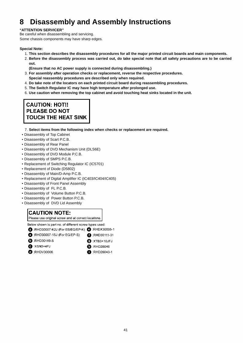
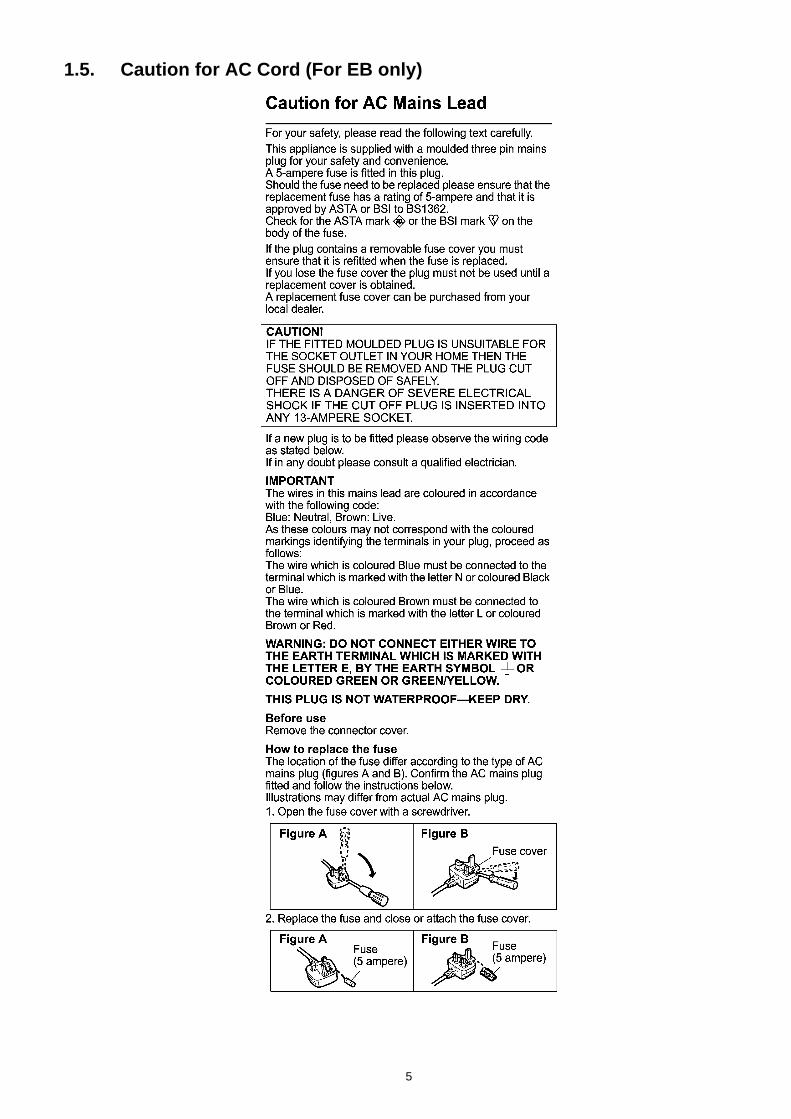
8 Disassembly and Assembly Instructions“ATTENTION SERVICER”Be careful when disassembling and servicing.Some chassis components may have sharp edges.
Special Note:1. This section describes the disassembly procedures for all the major printed circuit boards and main components. 2. Before the disassembly process was carried out, do take special note that all safety precautions are to be carried
out. (Ensure that no AC power supply is connected during disassembling.)
3. For assembly after operation checks or replacement, reverse the respective procedures.Special reassembly procedures are described only when required.
4. Do take note of the locators on each printed circuit board during reassembling procedures.5. The Switch Regulator IC may have high temperature after prolonged use. 6. Use caution when removing the top cabinet and avoid touching heat sinks located in the unit.
7. Select items from the following index when checks or replacement are required.• Disassembly of Top Cabinet• Disassembly of Scart P.C.B.• Disassembly of Rear Panel• Disassembly of DVD Mechanism Unit (DLS6E)• Disassembly of DVD Module P.C.B.• Disassembly of SMPS P.C.B.• Replacement of Switching Regulator IC (IC5701)• Replacement of Diode (D5802)• Disassembly of Main/D-Amp P.C.B.• Replacement of Digital Amplifier IC (IC403/IC404/IC405)• Disassembly of Front Panel Assembly• Disassembly of FL P.C.B.• Disassembly of Volume Button P.C.B.• Disassembly of Power Button P.C.B.• Disassembly of DVD Lid Assembly
41
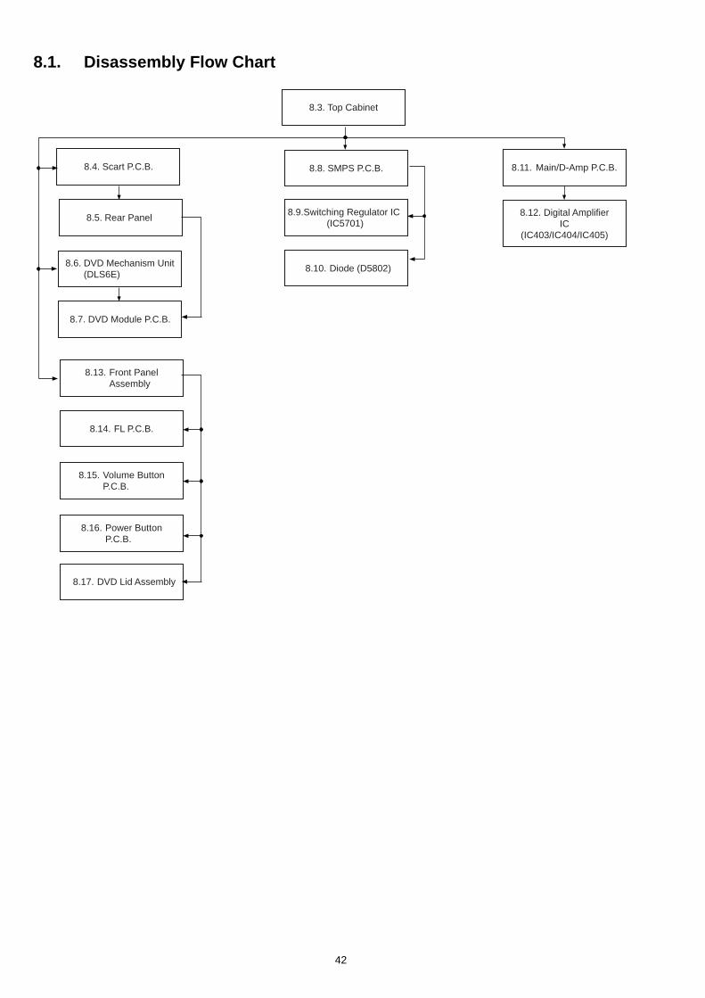
8.1. Disassembly Flow Chart
8.3. Top Cabinet
8.4. Scart P.C.B.
8.5. Rear Panel
8.7. DVD Module P.C.B.
8.8. SMPS P.C.B.
8.10. Diode (D5802)
8.11. Main/D-Amp P.C.B.
8.12. Digital Amplifier
IC
(IC403/IC404/IC405)
8.13. Front Panel
Assembly
8.14. FL P.C.B.
8.6. DVD Mechanism Unit
(DLS6E)
8.9.Switching Regulator IC
(IC5701)
8.15. Volume Button
P.C.B.
8.16. Power Button
P.C.B.
8.17. DVD Lid Assembly
42
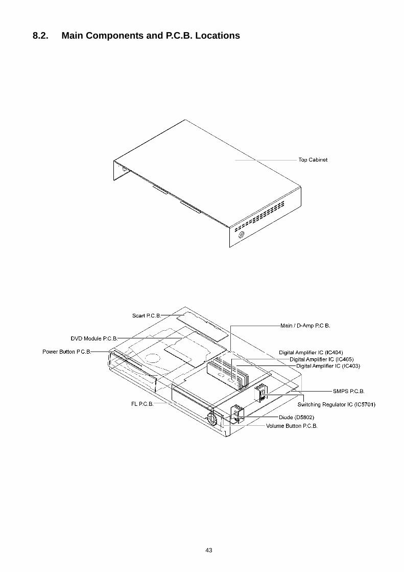
8.2. Main Components and P.C.B. Locations
43
8.3. Disassembly of Top Cabinet
Step 1 Remove 2 screws at the side of Top Cabinet
Step 2 Remove 3 screws at the rear of Top Cabinet.
Step 3 Lift up the back portion of Top Cabinet as arrow shown.
Step 4 Slightly lift both side of Top Cabinet in an outward direc-
tion as arrow shown.Step 5 Press left & right side at the top of front panel assemblyto release the catches and pull out Top Cabinet as arrowshown.
Step 6 Remove Top Cabinet as arrow shown.
8.4. Disassembly of Scart P.C.B.• Follow (Step 1) to (Step 6) of Item 8.3.
Step 1 Detach 17P FFC at the connector (CN4001) on ScartP.C.B..
Step 2 Remove 2 screws at the Rear Panel.
44
Step 3 Lift up to remove Scart P.C.B..
Caution: During assembling, ensure that Scart P.C.B. is properly located & fully catched onto rear panel.
8.5. Disassembly of Rear Panel• Follow (Step 1) to (Step 6) of Item 8.3.• Follow (Step 1) to (Step 3) of Item 8.4.
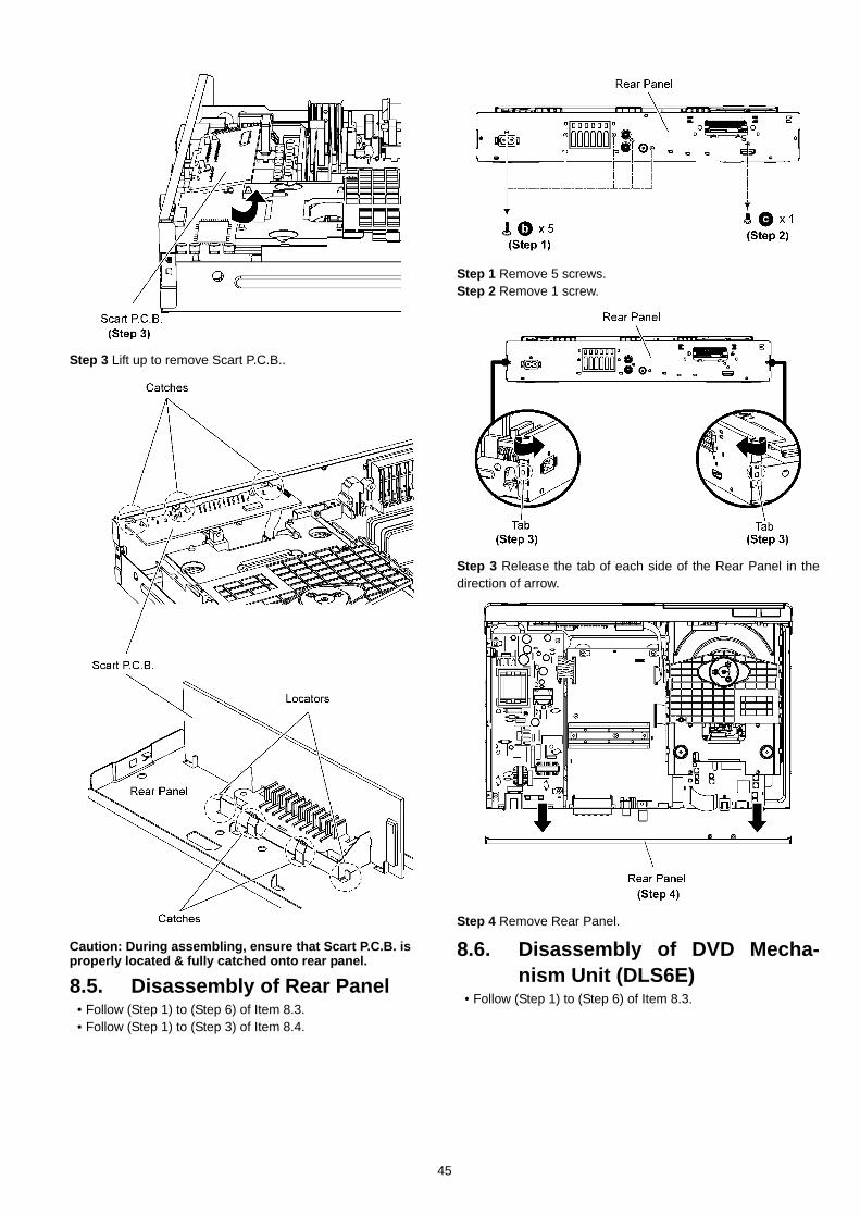
Step 1 Remove 5 screws.Step 2 Remove 1 screw.
Step 3 Release the tab of each side of the Rear Panel in thedirection of arrow.
Step 4 Remove Rear Panel.
8.6. Disassembly of DVD Mecha-nism Unit (DLS6E)
• Follow (Step 1) to (Step 6) of Item 8.3.
45
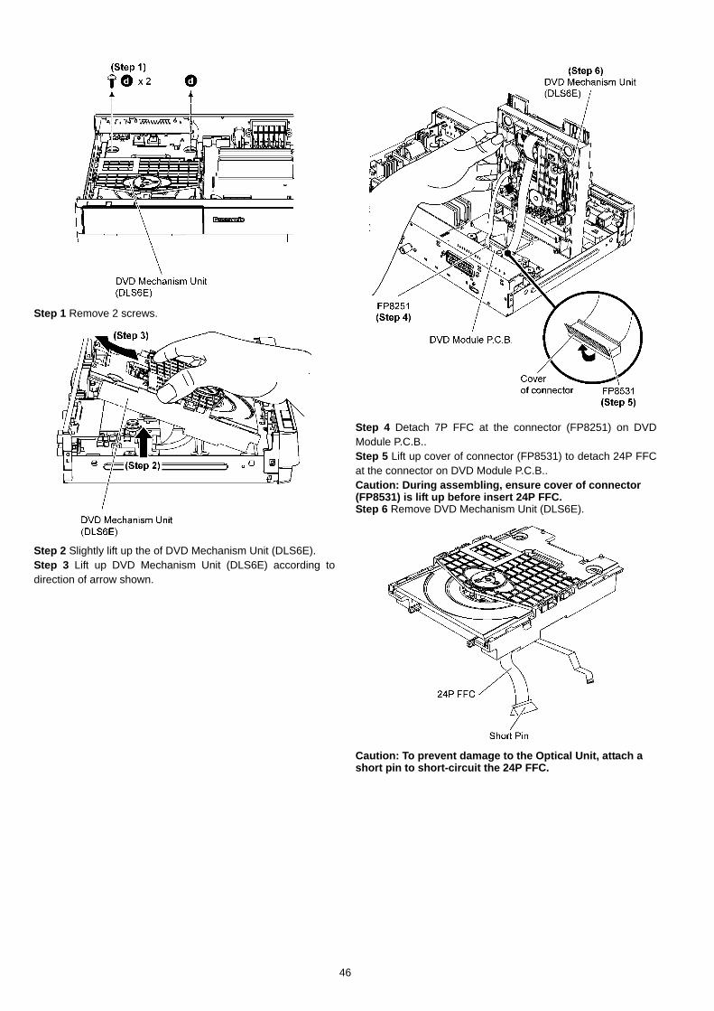
Step 1 Remove 2 screws.
Step 2 Slightly lift up the of DVD Mechanism Unit (DLS6E).Step 3 Lift up DVD Mechanism Unit (DLS6E) according todirection of arrow shown.
Step 4 Detach 7P FFC at the connector (FP8251) on DVDModule P.C.B..Step 5 Lift up cover of connector (FP8531) to detach 24P FFCat the connector on DVD Module P.C.B..Caution: During assembling, ensure cover of connector (FP8531) is lift up before insert 24P FFC.Step 6 Remove DVD Mechanism Unit (DLS6E).
Caution: To prevent damage to the Optical Unit, attach a short pin to short-circuit the 24P FFC.
46
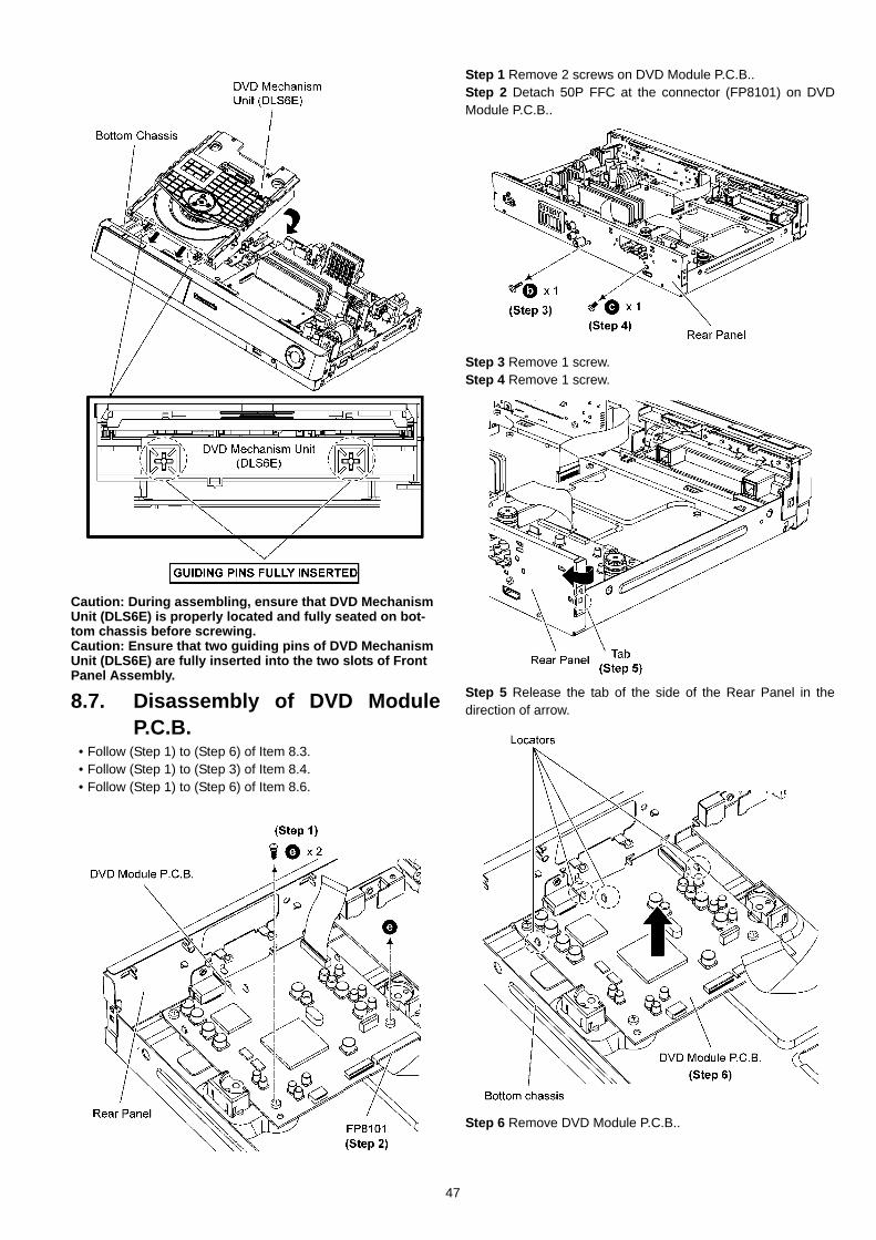
Caution: During assembling, ensure that DVD Mechanism Unit (DLS6E) is properly located and fully seated on bot-tom chassis before screwing.Caution: Ensure that two guiding pins of DVD Mechanism Unit (DLS6E) are fully inserted into the two slots of Front Panel Assembly.
8.7. Disassembly of DVD ModuleP.C.B.
• Follow (Step 1) to (Step 6) of Item 8.3.• Follow (Step 1) to (Step 3) of Item 8.4.• Follow (Step 1) to (Step 6) of Item 8.6.
Step 1 Remove 2 screws on DVD Module P.C.B..Step 2 Detach 50P FFC at the connector (FP8101) on DVDModule P.C.B..
Step 3 Remove 1 screw.Step 4 Remove 1 screw.
Step 5 Release the tab of the side of the Rear Panel in thedirection of arrow.
Step 6 Remove DVD Module P.C.B..
47
Caution: During assembling, ensure that DVD Module P.C.B. is properly located & fully seated onto bottom chas-sis.
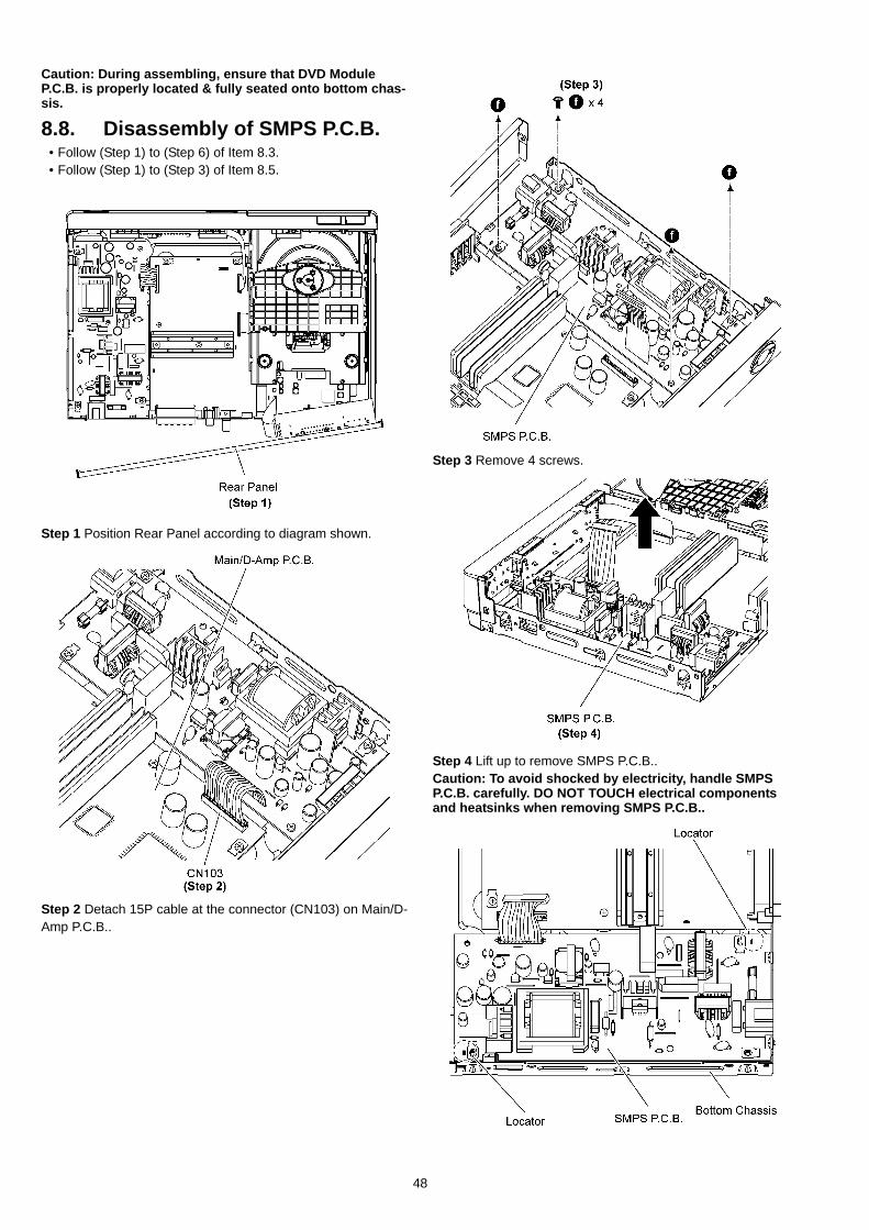
8.8. Disassembly of SMPS P.C.B.• Follow (Step 1) to (Step 6) of Item 8.3.• Follow (Step 1) to (Step 3) of Item 8.5.
Step 1 Position Rear Panel according to diagram shown.
Step 2 Detach 15P cable at the connector (CN103) on Main/D-Amp P.C.B..
Step 3 Remove 4 screws.
Step 4 Lift up to remove SMPS P.C.B..Caution: To avoid shocked by electricity, handle SMPS P.C.B. carefully. DO NOT TOUCH electrical components and heatsinks when removing SMPS P.C.B..
48
Caution: During assembling, ensure that SMPS P.C.B. is properly located & fully inserted onto Bottom Chassis.
8.9. Replacement of Switching Reg-ulator IC (IC5701)
• Follow (Step 1) to (Step 6) of Item 8.3.• Follow (Step 1) to (Step 3) of Item 8.5.• Follow (Step 1) to (Step 4) of Item 8.8.
8.9.1. Disassembly of Switching Regula-tor IC (IC5701)
Step 1 Desolder pins of the Switching Regulator IC (IC5701) onthe solder side of SMPS P.C.B..
Step 2 Remove 1 screw from the Switching Regulator IC(IC5701).Step 3 Remove the Switching Regulator IC (IC5701) from theHeatsink Ext A.Caution: Handle the Heatsink Ext A with caution due to its high temperature after prolonged use. Touching it may lead to injuries.Note Refer to the diagrams of SMPS P.C.B. (Item 18.4) forlocation of the part.
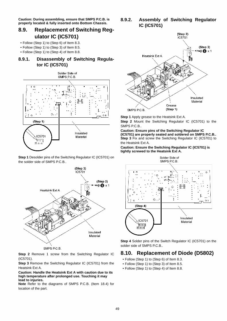
8.9.2. Assembly of Switching RegulatorIC (IC5701)
Step 1 Apply grease to the Heatsink Ext A.Step 2 Mount the Switching Regulator IC (IC5701) to theSMPS P.C.B..Caution: Ensure pins of the Switching Regulator IC (IC5701) are properly seated and soldered on SMPS P.C.B..Step 3 Fix and screw the Switching Regulator IC (IC5701) tothe Heatsink Ext A.Caution: Ensure the Switching Regulator IC (IC5701) is tightly screwed to the Heatsink Ext A.
Step 4 Solder pins of the Switch Regulator IC (IC5701) on thesolder side of SMPS P.C.B..
8.10. Replacement of Diode (D5802)• Follow (Step 1) to (Step 6) of Item 8.3.• Follow (Step 1) to (Step 3) of Item 8.5.• Follow (Step 1) to (Step 4) of Item 8.8.
49
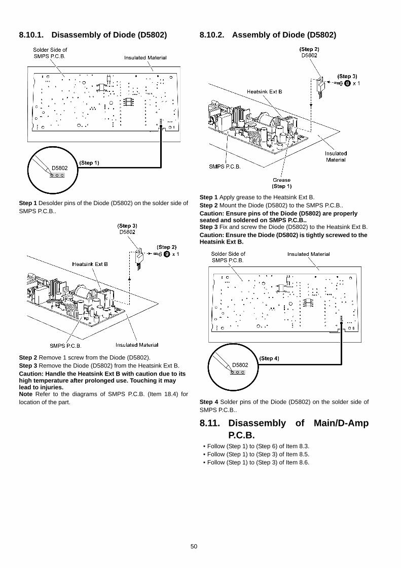
8.10.1. Disassembly of Diode (D5802)
Step 1 Desolder pins of the Diode (D5802) on the solder side ofSMPS P.C.B..
Step 2 Remove 1 screw from the Diode (D5802).Step 3 Remove the Diode (D5802) from the Heatsink Ext B.Caution: Handle the Heatsink Ext B with caution due to its high temperature after prolonged use. Touching it may lead to injuries.Note Refer to the diagrams of SMPS P.C.B. (Item 18.4) forlocation of the part.
8.10.2. Assembly of Diode (D5802)
Step 1 Apply grease to the Heatsink Ext B.Step 2 Mount the Diode (D5802) to the SMPS P.C.B..Caution: Ensure pins of the Diode (D5802) are properly seated and soldered on SMPS P.C.B..Step 3 Fix and screw the Diode (D5802) to the Heatsink Ext B.Caution: Ensure the Diode (D5802) is tightly screwed to the Heatsink Ext B.
Step 4 Solder pins of the Diode (D5802) on the solder side ofSMPS P.C.B..
8.11. Disassembly of Main/D-AmpP.C.B.
• Follow (Step 1) to (Step 6) of Item 8.3.• Follow (Step 1) to (Step 3) of Item 8.5.• Follow (Step 1) to (Step 3) of Item 8.6.
50
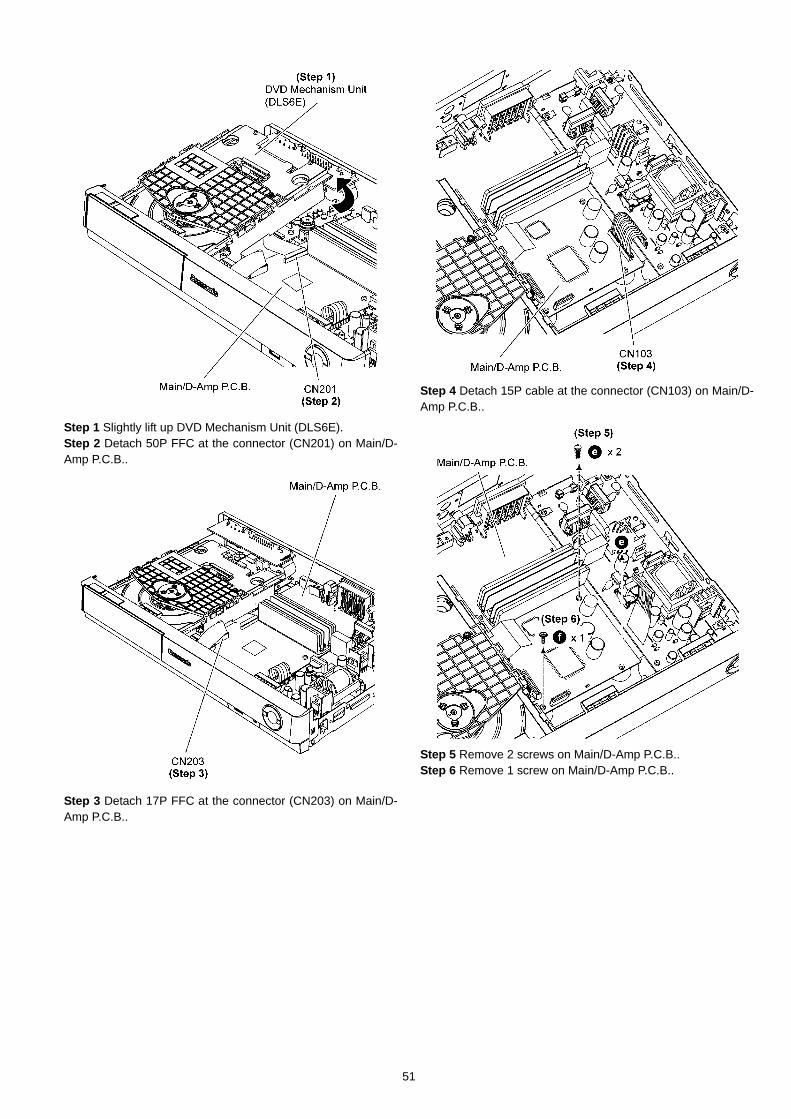
Step 1 Slightly lift up DVD Mechanism Unit (DLS6E).Step 2 Detach 50P FFC at the connector (CN201) on Main/D-Amp P.C.B..
Step 3 Detach 17P FFC at the connector (CN203) on Main/D-Amp P.C.B..
Step 4 Detach 15P cable at the connector (CN103) on Main/D-Amp P.C.B..
Step 5 Remove 2 screws on Main/D-Amp P.C.B..Step 6 Remove 1 screw on Main/D-Amp P.C.B..
51
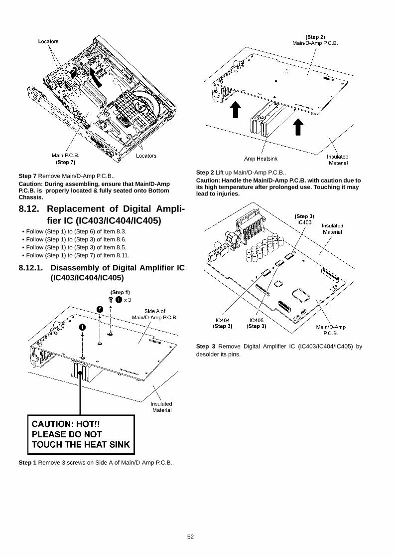
Step 7 Remove Main/D-Amp P.C.B..Caution: During assembling, ensure that Main/D-Amp P.C.B. is properly located & fully seated onto Bottom Chassis.
8.12. Replacement of Digital Ampli-fier IC (IC403/IC404/IC405)
• Follow (Step 1) to (Step 6) of Item 8.3.• Follow (Step 1) to (Step 3) of Item 8.6.• Follow (Step 1) to (Step 3) of Item 8.5.• Follow (Step 1) to (Step 7) of Item 8.11.
8.12.1. Disassembly of Digital Amplifier IC(IC403/IC404/IC405)
Step 1 Remove 3 screws on Side A of Main/D-Amp P.C.B..
Step 2 Lift up Main/D-Amp P.C.B..Caution: Handle the Main/D-Amp P.C.B. with caution due to its high temperature after prolonged use. Touching it may lead to injuries.
Step 3 Remove Digital Amplifier IC (IC403/IC404/IC405) bydesolder its pins.
52
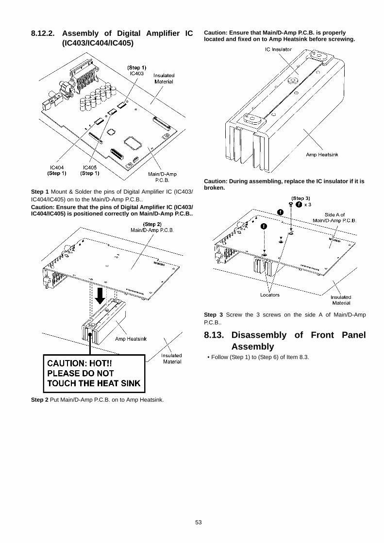
8.12.2. Assembly of Digital Amplifier IC(IC403/IC404/IC405)
Step 1 Mount & Solder the pins of Digital Amplifier IC (IC403/IC404/IC405) on to the Main/D-Amp P.C.B..Caution: Ensure that the pins of Digital Amplifier IC (IC403/IC404/IC405) is positioned correctly on Main/D-Amp P.C.B..
Step 2 Put Main/D-Amp P.C.B. on to Amp Heatsink.
Caution: Ensure that Main/D-Amp P.C.B. is properly located and fixed on to Amp Heatsink before screwing.
Caution: During assembling, replace the IC insulator if it is broken.
Step 3 Screw the 3 screws on the side A of Main/D-AmpP.C.B..
8.13. Disassembly of Front PanelAssembly
• Follow (Step 1) to (Step 6) of Item 8.3.
53
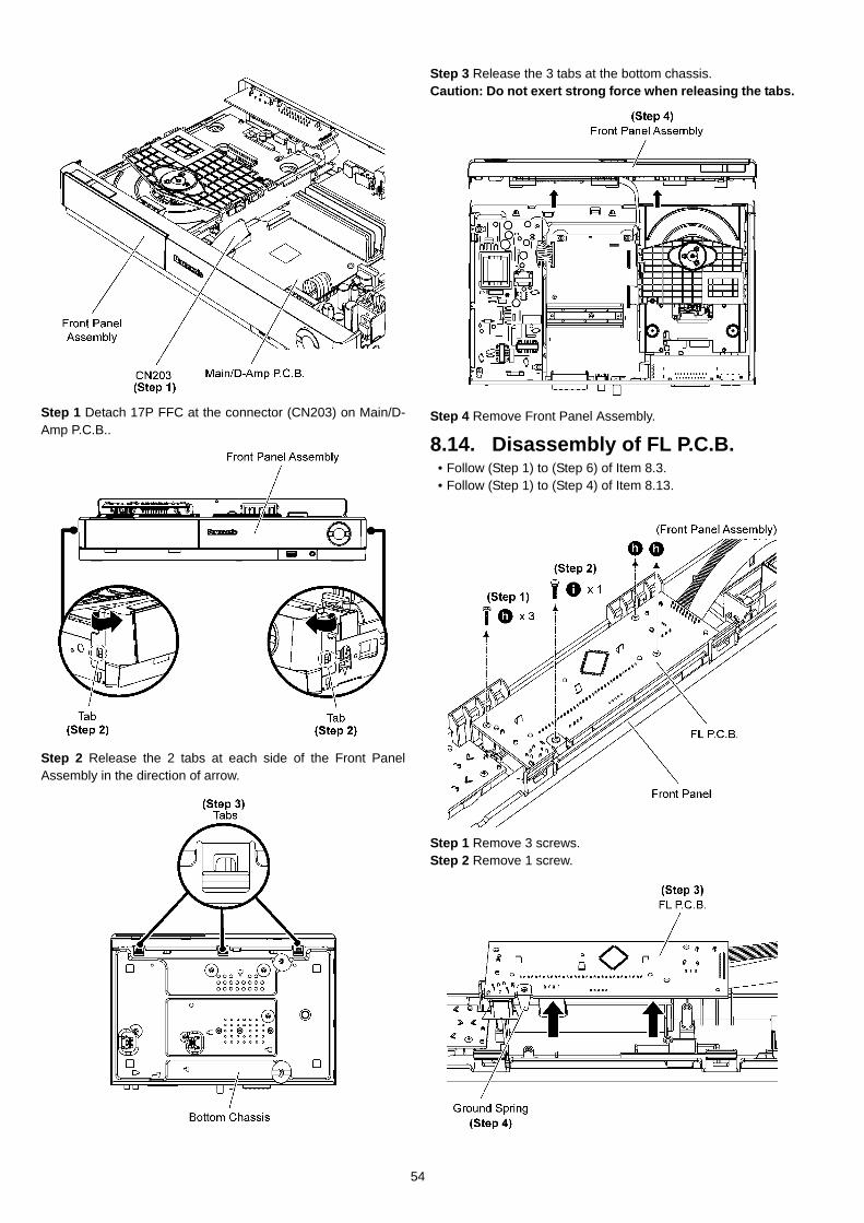
Step 1 Detach 17P FFC at the connector (CN203) on Main/D-Amp P.C.B..
Step 2 Release the 2 tabs at each side of the Front PanelAssembly in the direction of arrow.
Step 3 Release the 3 tabs at the bottom chassis.Caution: Do not exert strong force when releasing the tabs.
Step 4 Remove Front Panel Assembly.
8.14. Disassembly of FL P.C.B.• Follow (Step 1) to (Step 6) of Item 8.3.• Follow (Step 1) to (Step 4) of Item 8.13.
Step 1 Remove 3 screws.Step 2 Remove 1 screw.
54
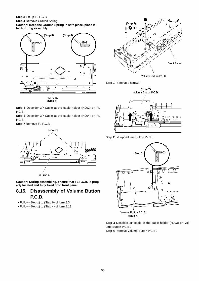
Step 3 Lift up FL P.C.B..Step 4 Remove Ground Spring.Caution: Keep the Ground Spring in safe place, place it back during assembly.
Step 5 Desolder 3P Cable at the cable holder (H902) on FLP.C.B..Step 6 Desolder 3P Cable at the cable holder (H904) on FLP.C.B..Step 7 Remove FL P.C.B..
Caution: During assembling, ensure that FL P.C.B. is prop-erly located and fully fixed onto front panel.
8.15. Disassembly of Volume ButtonP.C.B.
• Follow (Step 1) to (Step 6) of Item 8.3.• Follow (Step 1) to (Step 4) of Item 8.13.
Step 1 Remove 2 screws.
Step 2 Lift up Volume Button P.C.B..
Step 3 Desolder 3P cable at the cable holder (H903) on Vol-ume Button P.C.B..Step 4 Remove Volume Button P.C.B..
55
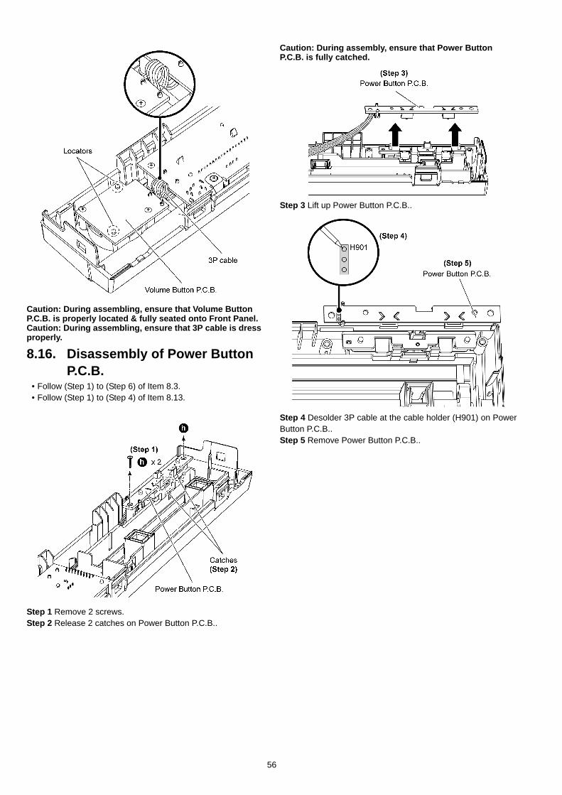
Caution: During assembling, ensure that Volume Button P.C.B. is properly located & fully seated onto Front Panel.Caution: During assembling, ensure that 3P cable is dress properly.
8.16. Disassembly of Power Button P.C.B.
• Follow (Step 1) to (Step 6) of Item 8.3.• Follow (Step 1) to (Step 4) of Item 8.13.
Step 1 Remove 2 screws.Step 2 Release 2 catches on Power Button P.C.B..
Caution: During assembly, ensure that Power Button P.C.B. is fully catched.
Step 3 Lift up Power Button P.C.B..
Step 4 Desolder 3P cable at the cable holder (H901) on PowerButton P.C.B..Step 5 Remove Power Button P.C.B..
56
Caution: During assembling, ensure that Power Button P.C.B. is properly located & fully catched onto Front Panel with 3P cable dressed according to diagram shown.
8.17. Replacement of DVD LidAssembly
• Follow (Step 1) to (Step 6) of Item 8.3.• Follow (Step 1) to (Step 4) of Item 8.15.
8.17.1. Disassembly of DVD LidAssembly
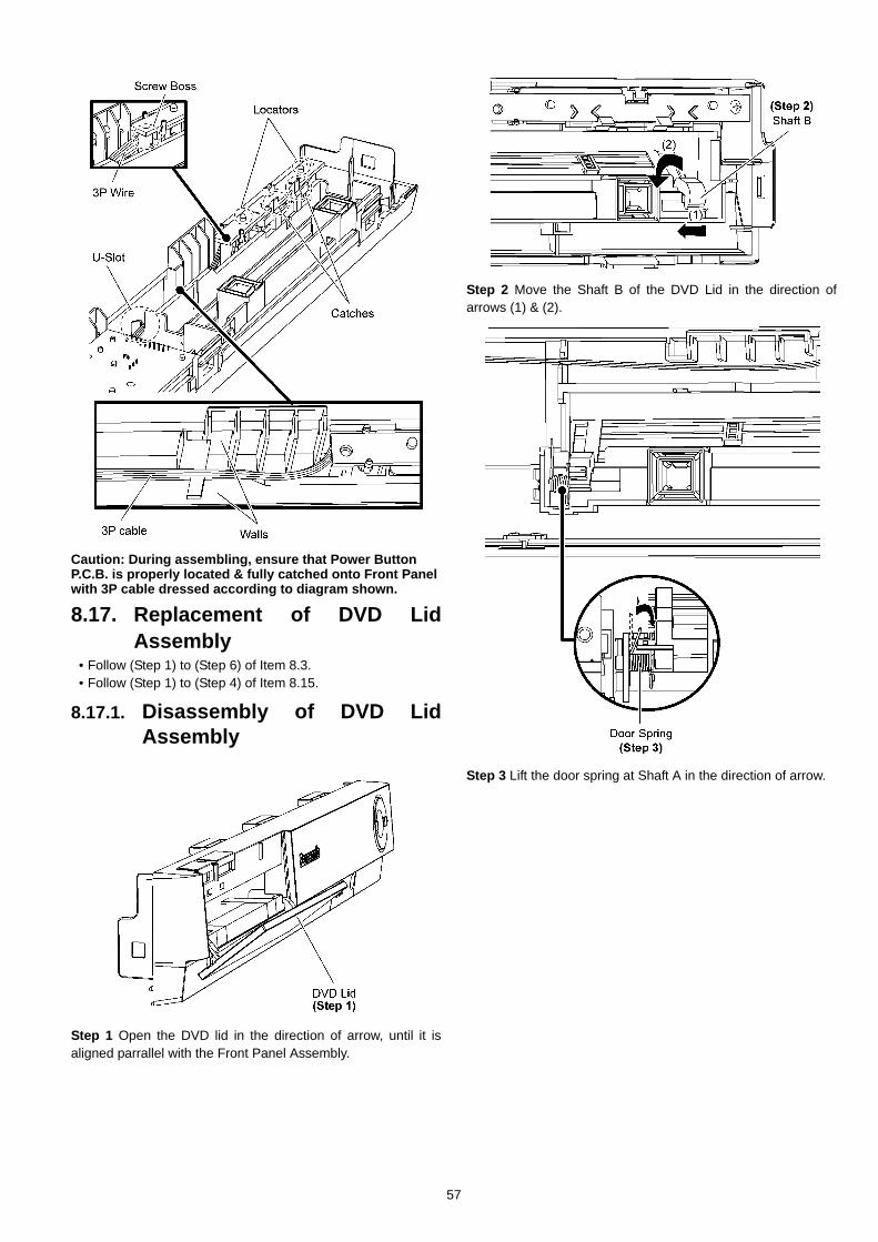
Step 1 Open the DVD lid in the direction of arrow, until it isaligned parrallel with the Front Panel Assembly.
Step 2 Move the Shaft B of the DVD Lid in the direction ofarrows (1) & (2).
Step 3 Lift the door spring at Shaft A in the direction of arrow.
57
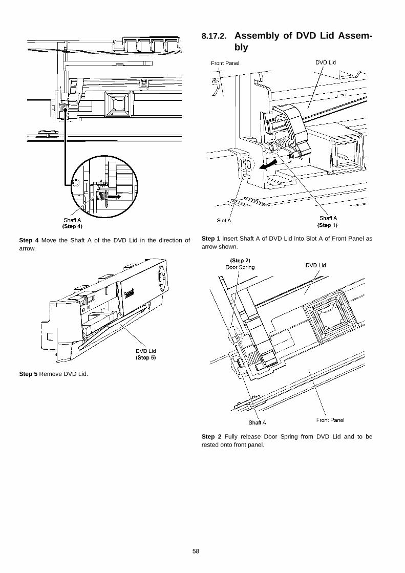
Step 4 Move the Shaft A of the DVD Lid in the direction ofarrow.
Step 5 Remove DVD Lid.
8.17.2. Assembly of DVD Lid Assem-bly
Step 1 Insert Shaft A of DVD Lid into Slot A of Front Panel asarrow shown.
Step 2 Fully release Door Spring from DVD Lid and to berested onto front panel.
58
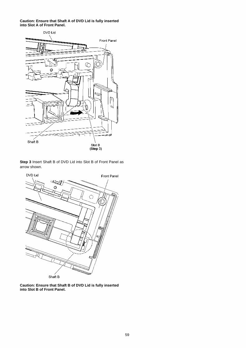
Caution: Ensure that Shaft A of DVD Lid is fully inserted into Slot A of Front Panel.
Step 3 Insert Shaft B of DVD Lid into Slot B of Front Panel asarrow shown.
Caution: Ensure that Shaft B of DVD Lid is fully inserted into Slot B of Front Panel.
59
9 Assembling and Disas-sembling of Traverse Unit
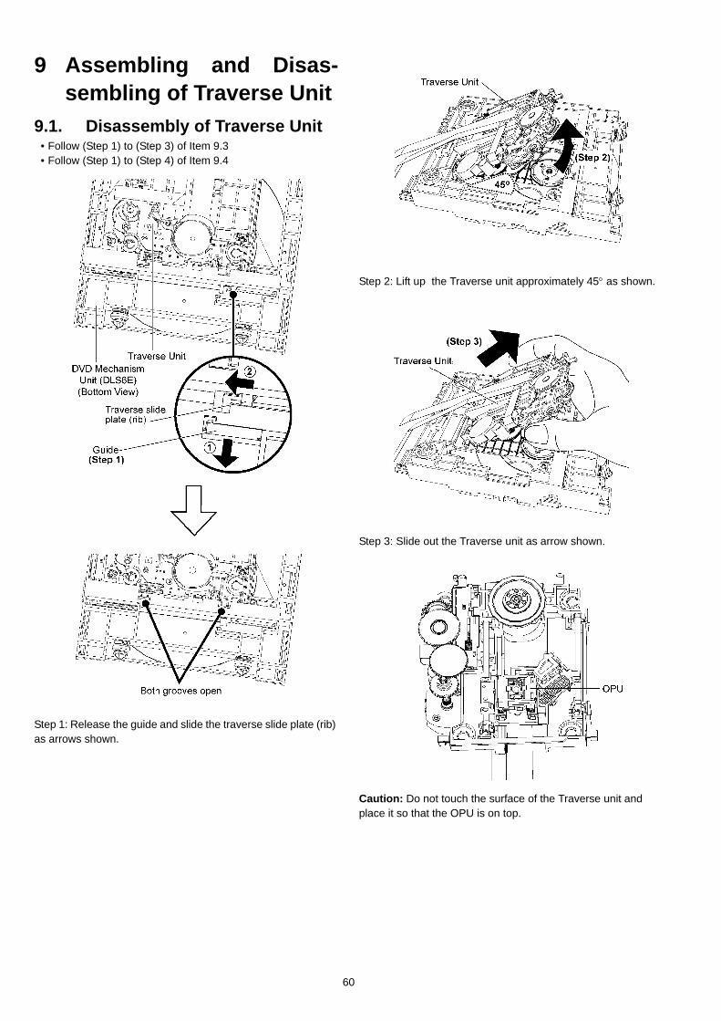
9.1. Disassembly of Traverse Unit• Follow (Step 1) to (Step 3) of Item 9.3• Follow (Step 1) to (Step 4) of Item 9.4
Step 1: Release the guide and slide the traverse slide plate (rib) as arrows shown.
Step 2: Lift up the Traverse unit approximately 45° as shown.
Step 3: Slide out the Traverse unit as arrow shown.
Caution: Do not touch the surface of the Traverse unit and place it so that the OPU is on top.
60
9.2. Assembly of Traverse Unit
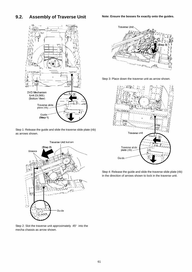
Step 1: Release the guide and slide the traverse slide plate (rib) as arrows shown.
Step 2: Slot the traverse unit approximately 45° into the mecha chassis as arrow shown.
Note: Ensure the bosses fix exactly onto the guides.
Step 3: Place down the traverse unit as arrow shown.
Step 4: Release the guide and slide the traverse slide plate (rib) in the direction of arrows shown to lock in the traverse unit.
61
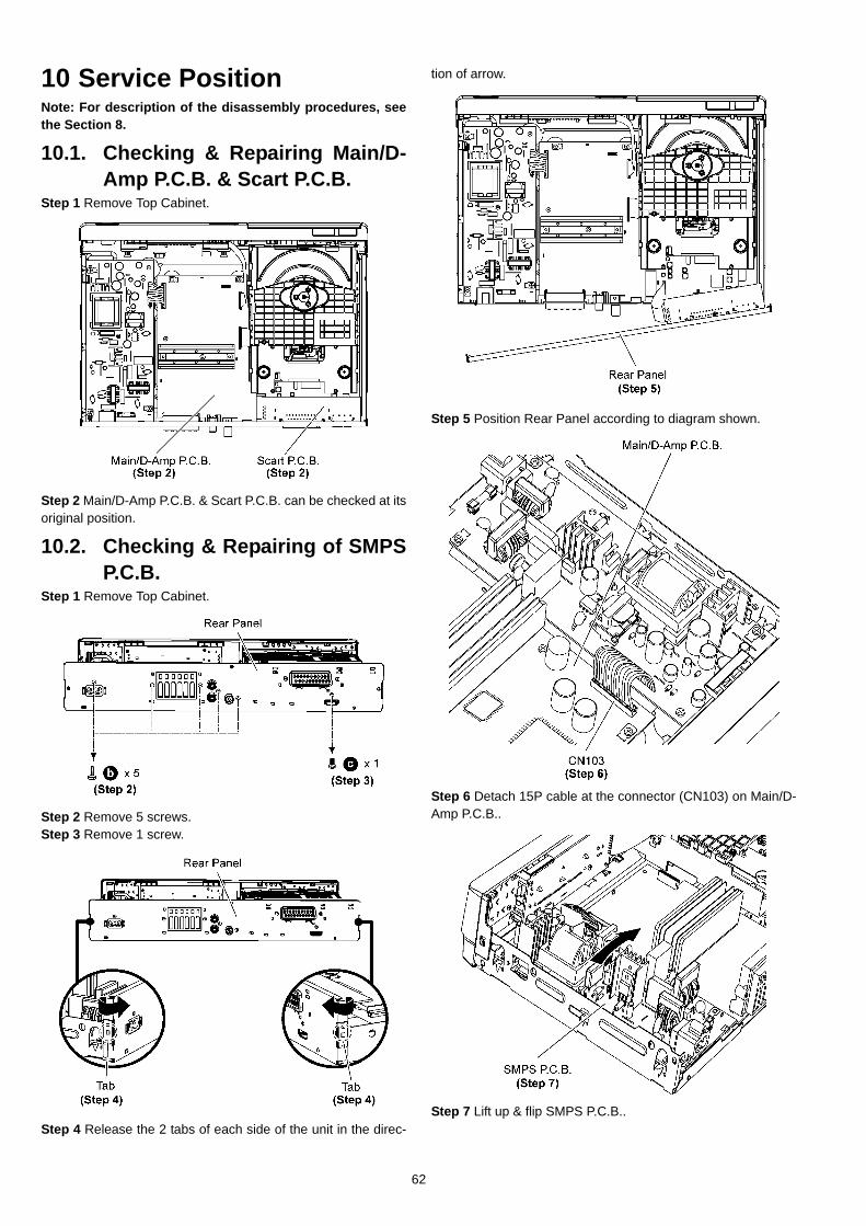
10 Service PositionNote: For description of the disassembly procedures, seethe Section 8.
10.1. Checking & Repairing Main/D-Amp P.C.B. & Scart P.C.B.
Step 1 Remove Top Cabinet.
Step 2 Main/D-Amp P.C.B. & Scart P.C.B. can be checked at itsoriginal position.
10.2. Checking & Repairing of SMPSP.C.B.
Step 1 Remove Top Cabinet.
Step 2 Remove 5 screws.Step 3 Remove 1 screw.
Step 4 Release the 2 tabs of each side of the unit in the direc-
tion of arrow.
Step 5 Position Rear Panel according to diagram shown.
Step 6 Detach 15P cable at the connector (CN103) on Main/D-Amp P.C.B..
Step 7 Lift up & flip SMPS P.C.B..
62
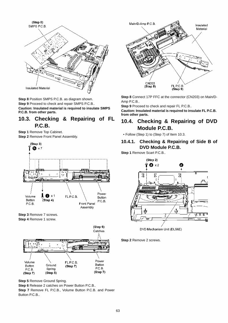
Step 8 Position SMPS P.C.B. as diagram shown.Step 9 Proceed to check and repair SMPS P.C.B..Caution: Insulated material is required to insulate SMPS P.C.B. from other parts.
10.3. Checking & Repairing of FLP.C.B.
Step 1 Remove Top Cabinet.Step 2 Remove Front Panel Assembly.
Step 3 Remove 7 screws.Step 4 Remove 1 screw.
Step 5 Remove Ground Spring.Step 6 Release 2 catches on Power Button P.C.B..Step 7 Remove FL P.C.B., Volume Button P.C.B. and PowerButton P.C.B..
Step 8 Connect 17P FFC at the connector (CN203) on Main/D-Amp P.C.B..Step 9 Proceed to check and repair FL P.C.B..Caution: Insulated material is required to insulate FL P.C.B. from other parts.
10.4. Checking & Repairing of DVDModule P.C.B.
• Follow (Step 1) to (Step 7) of Item 10.3.
10.4.1. Checking & Repairing of Side B ofDVD Module P.C.B.
Step 1 Remove Scart P.C.B..
Step 2 Remove 2 screws.
63
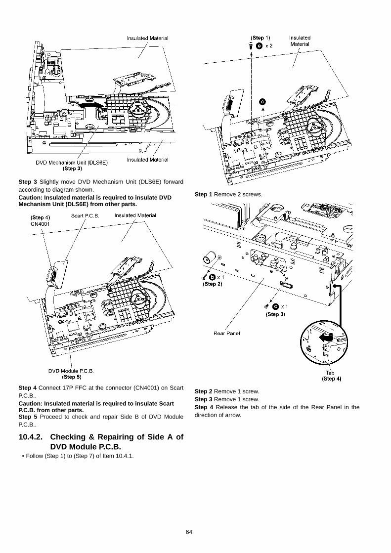
Step 3 Slightly move DVD Mechanism Unit (DLS6E) forwardaccording to diagram shown.Caution: Insulated material is required to insulate DVD Mechanism Unit (DLS6E) from other parts.
Step 4 Connect 17P FFC at the connector (CN4001) on ScartP.C.B..Caution: Insulated material is required to insulate Scart P.C.B. from other parts.Step 5 Proceed to check and repair Side B of DVD ModuleP.C.B..
10.4.2. Checking & Repairing of Side A ofDVD Module P.C.B.
• Follow (Step 1) to (Step 7) of Item 10.4.1.
Step 1 Remove 2 screws.
Step 2 Remove 1 screw.Step 3 Remove 1 screw.Step 4 Release the tab of the side of the Rear Panel in thedirection of arrow.
64
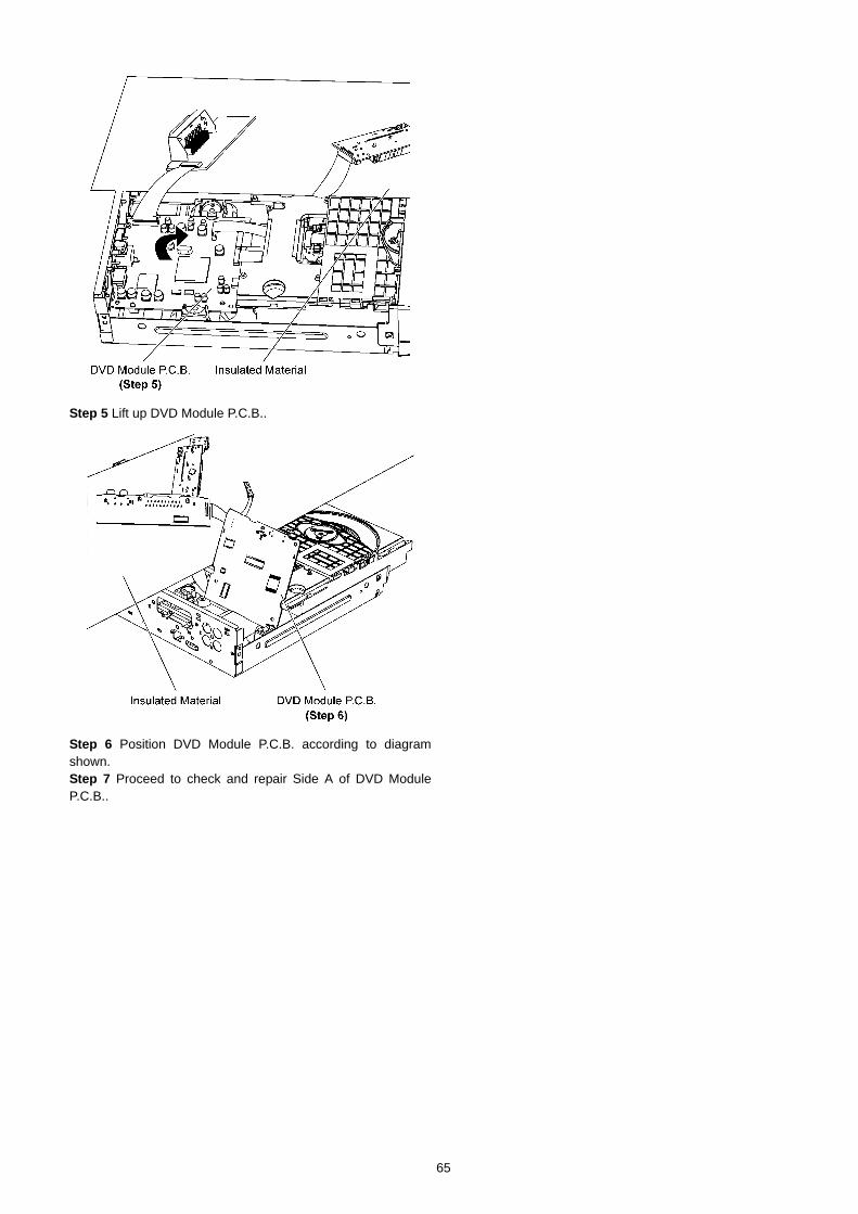
Step 5 Lift up DVD Module P.C.B..
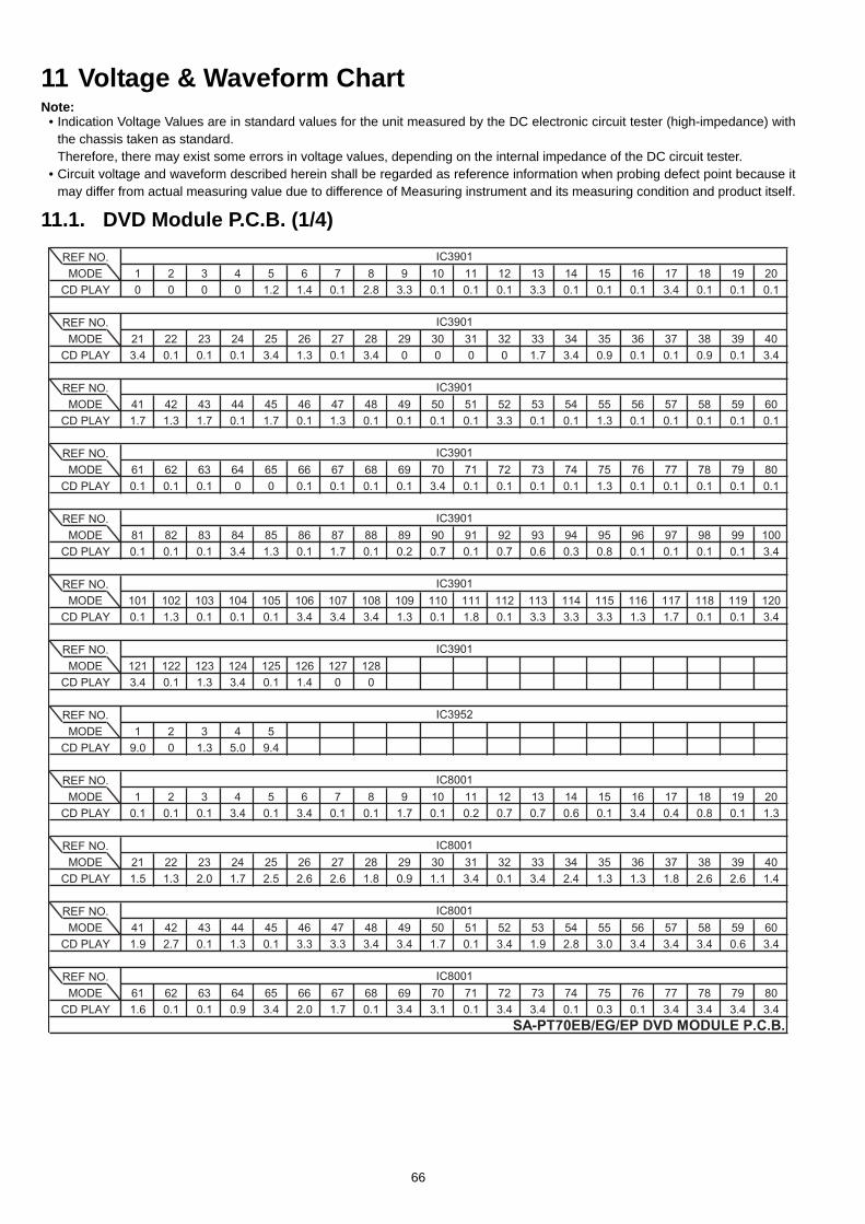
Step 6 Position DVD Module P.C.B. according to diagramshown.Step 7 Proceed to check and repair Side A of DVD ModuleP.C.B..
65
11 Voltage & Waveform ChartNote:
• Indication Voltage Values are in standard values for the unit measured by the DC electronic circuit tester (high-impedance) withthe chassis taken as standard.Therefore, there may exist some errors in voltage values, depending on the internal impedance of the DC circuit tester.
• Circuit voltage and waveform described herein shall be regarded as reference information when probing defect point because itmay differ from actual measuring value due to difference of Measuring instrument and its measuring condition and product itself.
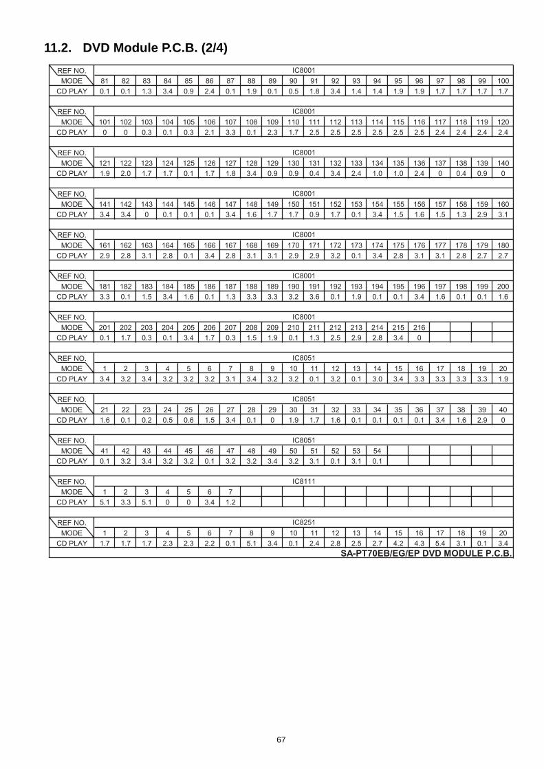
11.1. DVD Module P.C.B. (1/4)
REF NO.MODE 1 2 3 4 5 6 7 8 9 10 11 12 13 14 15 16 17 18 19 20
CD PLAY 0 0 0 0 1.2 1.4 0.1 2.8 3.3 0.1 0.1 0.1 3.3 0.1 0.1 0.1 3.4 0.1 0.1 0.1
REF NO.MODE 21 22 23 24 25 26 27 28 29 30 31 32 33 34 35 36 37 38 39 40
CD PLAY 3.4 0.1 0.1 0.1 3.4 1.3 0.1 3.4 0 0 0 0 1.7 3.4 0.9 0.1 0.1 0.9 0.1 3.4
REF NO.MODE 41 42 43 44 45 46 47 48 49 50 51 52 53 54 55 56 57 58 59 60
CD PLAY 1.7 1.3 1.7 0.1 1.7 0.1 1.3 0.1 0.1 0.1 0.1 3.3 0.1 0.1 1.3 0.1 0.1 0.1 0.1 0.1
REF NO.MODE 61 62 63 64 65 66 67 68 69 70 71 72 73 74 75 76 77 78 79 80
CD PLAY 0.1 0.1 0.1 0 0 0.1 0.1 0.1 0.1 3.4 0.1 0.1 0.1 0.1 1.3 0.1 0.1 0.1 0.1 0.1
REF NO.MODE 81 82 83 84 85 86 87 88 89 90 91 92 93 94 95 96 97 98 99 100
CD PLAY 0.1 0.1 0.1 3.4 1.3 0.1 1.7 0.1 0.2 0.7 0.1 0.7 0.6 0.3 0.8 0.1 0.1 0.1 0.1 3.4
REF NO.MODE 101 102 103 104 105 106 107 108 109 110 111 112 113 114 115 116 117 118 119 120
CD PLAY 0.1 1.3 0.1 0.1 0.1 3.4 3.4 3.4 1.3 0.1 1.8 0.1 3.3 3.3 3.3 1.3 1.7 0.1 0.1 3.4
REF NO.MODE 121 122 123 124 125 126 127 128
CD PLAY 3.4 0.1 1.3 3.4 0.1 1.4 0 0
REF NO.MODE 1 2 3 4 5
CD PLAY 9.0 0 1.3 5.0 9.4
REF NO.MODE 1 2 3 4 5 6 7 8 9 10 11 12 13 14 15 16 17 18 19 20
CD PLAY 0.1 0.1 0.1 3.4 0.1 3.4 0.1 0.1 1.7 0.1 0.2 0.7 0.7 0.6 0.1 3.4 0.4 0.8 0.1 1.3
REF NO.MODE 21 22 23 24 25 26 27 28 29 30 31 32 33 34 35 36 37 38 39 40
CD PLAY 1.5 1.3 2.0 1.7 2.5 2.6 2.6 1.8 0.9 1.1 3.4 0.1 3.4 2.4 1.3 1.3 1.8 2.6 2.6 1.4
REF NO.MODE 41 42 43 44 45 46 47 48 49 50 51 52 53 54 55 56 57 58 59 60
CD PLAY 1.9 2.7 0.1 1.3 0.1 3.3 3.3 3.4 3.4 1.7 0.1 3.4 1.9 2.8 3.0 3.4 3.4 3.4 0.6 3.4
REF NO.MODE 61 62 63 64 65 66 67 68 69 70 71 72 73 74 75 76 77 78 79 80
CD PLAY 1.6 0.1 0.1 0.9 3.4 2.0 1.7 0.1 3.4 3.1 0.1 3.4 3.4 0.1 0.3 0.1 3.4 3.4 3.4 3.4
IC3901
IC3901
IC3952
IC8001
IC3901
IC3901
IC3901
IC3901
IC3901
SA-PT70EB/EG/EP DVD MODULE P.C.B.
IC8001
IC8001
IC8001
66
11.2. DVD Module P.C.B. (2/4)
REF NO.MODE 81 82 83 84 85 86 87 88 89 90 91 92 93 94 95 96 97 98 99 100
CD PLAY 0.1 0.1 1.3 3.4 0.9 2.4 0.1 1.9 0.1 0.5 1.8 3.4 1.4 1.4 1.9 1.9 1.7 1.7 1.7 1.7
REF NO.MODE 101 102 103 104 105 106 107 108 109 110 111 112 113 114 115 116 117 118 119 120
CD PLAY 0 0 0.3 0.1 0.3 2.1 3.3 0.1 2.3 1.7 2.5 2.5 2.5 2.5 2.5 2.5 2.4 2.4 2.4 2.4
REF NO.MODE 121 122 123 124 125 126 127 128 129 130 131 132 133 134 135 136 137 138 139 140
CD PLAY 1.9 2.0 1.7 1.7 0.1 1.7 1.8 3.4 0.9 0.9 0.4 3.4 2.4 1.0 1.0 2.4 0 0.4 0.9 0
REF NO.MODE 141 142 143 144 145 146 147 148 149 150 151 152 153 154 155 156 157 158 159 160
CD PLAY 3.4 3.4 0 0.1 0.1 0.1 3.4 1.6 1.7 1.7 0.9 1.7 0.1 3.4 1.5 1.6 1.5 1.3 2.9 3.1
REF NO.MODE 161 162 163 164 165 166 167 168 169 170 171 172 173 174 175 176 177 178 179 180
CD PLAY 2.9 2.8 3.1 2.8 0.1 3.4 2.8 3.1 3.1 2.9 2.9 3.2 0.1 3.4 2.8 3.1 3.1 2.8 2.7 2.7
REF NO.MODE 181 182 183 184 185 186 187 188 189 190 191 192 193 194 195 196 197 198 199 200
CD PLAY 3.3 0.1 1.5 3.4 1.6 0.1 1.3 3.3 3.3 3.2 3.6 0.1 1.9 0.1 0.1 3.4 1.6 0.1 0.1 1.6
REF NO.MODE 201 202 203 204 205 206 207 208 209 210 211 212 213 214 215 216
CD PLAY 0.1 1.7 0.3 0.1 3.4 1.7 0.3 1.5 1.9 0.1 1.3 2.5 2.9 2.8 3.4 0
REF NO.MODE 1 2 3 4 5 6 7 8 9 10 11 12 13 14 15 16 17 18 19 20
CD PLAY 3.4 3.2 3.4 3.2 3.2 3.2 3.1 3.4 3.2 3.2 0.1 3.2 0.1 3.0 3.4 3.3 3.3 3.3 3.3 1.9
REF NO.MODE 21 22 23 24 25 26 27 28 29 30 31 32 33 34 35 36 37 38 39 40
CD PLAY 1.6 0.1 0.2 0.5 0.6 1.5 3.4 0.1 0 1.9 1.7 1.6 0.1 0.1 0.1 0.1 3.4 1.6 2.9 0
REF NO.MODE 41 42 43 44 45 46 47 48 49 50 51 52 53 54
CD PLAY 0.1 3.2 3.4 3.2 3.2 0.1 3.2 3.2 3.4 3.2 3.1 0.1 3.1 0.1
REF NO.MODE 1 2 3 4 5 6 7
CD PLAY 5.1 3.3 5.1 0 0 3.4 1.2
REF NO.MODE 1 2 3 4 5 6 7 8 9 10 11 12 13 14 15 16 17 18 19 20
CD PLAY 1.7 1.7 1.7 2.3 2.3 2.2 0.1 5.1 3.4 0.1 2.4 2.8 2.5 2.7 4.2 4.3 5.4 3.1 0.1 3.4
IC8001
IC8001
IC8051
IC8051
IC8001
IC8001
IC8001
IC8001
IC8001
SA-PT70EB/EG/EP DVD MODULE P.C.B.
IC8111
IC8051
IC8251
67
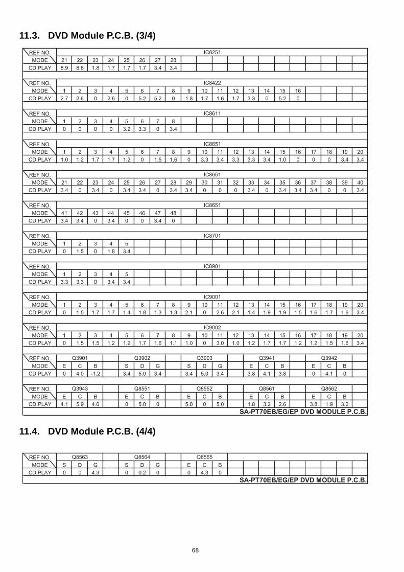
11.3. DVD Module P.C.B. (3/4)
11.4. DVD Module P.C.B. (4/4)
REF NO.MODE 21 22 23 24 25 26 27 28
CD PLAY 8.9 8.8 1.8 1.7 1.7 1.7 3.4 3.4
REF NO.MODE 1 2 3 4 5 6 7 8 9 10 11 12 13 14 15 16
CD PLAY 2.7 2.6 0 2.6 0 5.2 5.2 0 1.8 1.7 1.6 1.7 3.3 0 5.2 0
REF NO.MODE 1 2 3 4 5 6 7 8
CD PLAY 0 0 0 0 3.2 3.3 0 3.4
REF NO.MODE 1 2 3 4 5 6 7 8 9 10 11 12 13 14 15 16 17 18 19 20
CD PLAY 1.0 1.2 1.7 1.7 1.2 0 1.5 1.6 0 3.3 3.4 3.3 3.3 3.4 1.0 0 0 0 3.4 3.4
REF NO.MODE 21 22 23 24 25 26 27 28 29 30 31 32 33 34 35 36 37 38 39 40
CD PLAY 3.4 0 3.4 0 3.4 3.4 0 3.4 3.4 0 0 0 3.4 0 3.4 3.4 3.4 0 0 3.4
REF NO.MODE 41 42 43 44 45 46 47 48
CD PLAY 3.4 3.4 0 3.4 0 0 3.4 0
REF NO.MODE 1 2 3 4 5
CD PLAY 0 1.5 0 1.8 3.4
REF NO.MODE 1 2 3 4 5
CD PLAY 3.3 3.3 0 3.4 3.4
REF NO.MODE 1 2 3 4 5 6 7 8 9 10 11 12 13 14 15 16 17 18 19 20
CD PLAY 0 1.5 1.7 1.7 1.4 1.8 1.3 1.3 2.1 0 2.6 2.1 1.4 1.9 1.9 1.5 1.6 1.7 1.6 3.4
REF NO.MODE 1 2 3 4 5 6 7 8 9 10 11 12 13 14 15 16 17 18 19 20
CD PLAY 0 1.5 1.5 1.2 1.2 1.7 1.6 1.1 1.0 0 3.0 1.0 1.2 1.7 1.7 1.2 1.2 1.5 1.6 3.4
REF NO.MODE E C B S D G S D G E C B E C B
CD PLAY 0 4.0 -1.2 3.4 5.0 3.4 3.4 5.0 3.4 3.8 4.1 3.8 0 4.1 0
REF NO.MODE E C B E C B E C B E C B E C B
CD PLAY 4.1 5.9 4.6 0 5.0 0 5.0 0 5.0 1.8 3.2 2.6 3.8 1.9 3.2
SA-PT70EB/EG/EP DVD MODULE P.C.B.
IC9002
Q3901 Q3902 Q3903 Q3941 Q3942
Q3943
IC8251
IC8422
IC8611
IC8651
IC8651
IC8701
IC8901
IC9001
IC8651
Q8551 Q8552 Q8561 Q8562
REF NO.MODE S D G S D G E C B
CD PLAY 0 0 4.3 0 0.2 0 0 4.3 0
Q8563 Q8564 Q8565
SA-PT70EB/EG/EP DVD MODULE P.C.B.
68
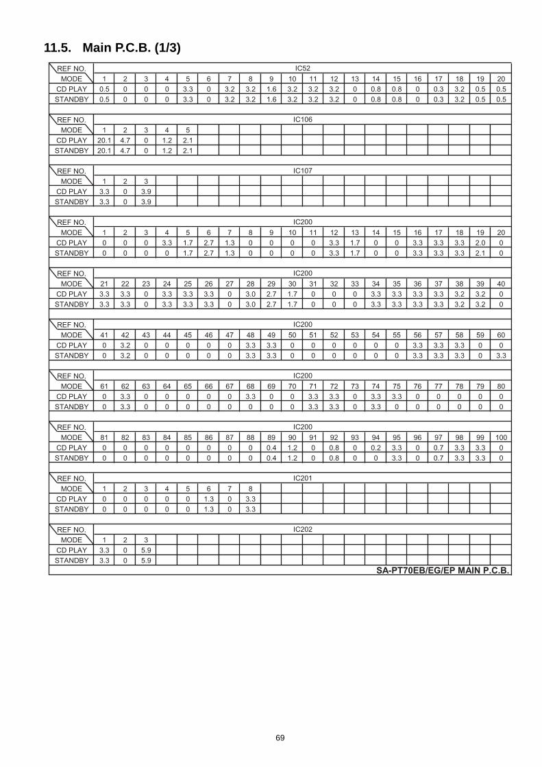
11.5. Main P.C.B. (1/3)
REF NO.MODE 1 2 3 4 5 6 7 8 9 10 11 12 13 14 15 16 17 18 19 20
CD PLAY 0.5 0 0 0 3.3 0 3.2 3.2 1.6 3.2 3.2 3.2 0 0.8 0.8 0 0.3 3.2 0.5 0.5STANDBY 0.5 0 0 0 3.3 0 3.2 3.2 1.6 3.2 3.2 3.2 0 0.8 0.8 0 0.3 3.2 0.5 0.5
REF NO.MODE 1 2 3 4 5
CD PLAY 20.1 4.7 0 1.2 2.1STANDBY 20.1 4.7 0 1.2 2.1
REF NO.MODE 1 2 3
CD PLAY 3.3 0 3.9STANDBY 3.3 0 3.9
REF NO.MODE 1 2 3 4 5 6 7 8 9 10 11 12 13 14 15 16 17 18 19 20
CD PLAY 0 0 0 3.3 1.7 2.7 1.3 0 0 0 0 3.3 1.7 0 0 3.3 3.3 3.3 2.0 0STANDBY 0 0 0 0 1.7 2.7 1.3 0 0 0 0 3.3 1.7 0 0 3.3 3.3 3.3 2.1 0
REF NO.MODE 21 22 23 24 25 26 27 28 29 30 31 32 33 34 35 36 37 38 39 40
CD PLAY 3.3 3.3 0 3.3 3.3 3.3 0 3.0 2.7 1.7 0 0 0 3.3 3.3 3.3 3.3 3.2 3.2 0STANDBY 3.3 3.3 0 3.3 3.3 3.3 0 3.0 2.7 1.7 0 0 0 3.3 3.3 3.3 3.3 3.2 3.2 0
REF NO.MODE 41 42 43 44 45 46 47 48 49 50 51 52 53 54 55 56 57 58 59 60
CD PLAY 0 3.2 0 0 0 0 0 3.3 3.3 0 0 0 0 0 0 3.3 3.3 3.3 0 0STANDBY 0 3.2 0 0 0 0 0 3.3 3.3 0 0 0 0 0 0 3.3 3.3 3.3 0 3.3
REF NO.MODE 61 62 63 64 65 66 67 68 69 70 71 72 73 74 75 76 77 78 79 80
CD PLAY 0 3.3 0 0 0 0 0 3.3 0 0 3.3 3.3 0 3.3 3.3 0 0 0 0 0STANDBY 0 3.3 0 0 0 0 0 0 0 0 3.3 3.3 0 3.3 0 0 0 0 0 0
REF NO.MODE 81 82 83 84 85 86 87 88 89 90 91 92 93 94 95 96 97 98 99 100
CD PLAY 0 0 0 0 0 0 0 0 0.4 1.2 0 0.8 0 0.2 3.3 0 0.7 3.3 3.3 0STANDBY 0 0 0 0 0 0 0 0 0.4 1.2 0 0.8 0 0 3.3 0 0.7 3.3 3.3 0
REF NO.MODE 1 2 3 4 5 6 7 8
CD PLAY 0 0 0 0 0 1.3 0 3.3STANDBY 0 0 0 0 0 1.3 0 3.3
REF NO.MODE 1 2 3
CD PLAY 3.3 0 5.9STANDBY 3.3 0 5.9
IC202
SA-PT70EB/EG/EP MAIN P.C.B.
IC52
IC201
IC200
IC200
IC200
IC106
IC107
IC200
IC200
69
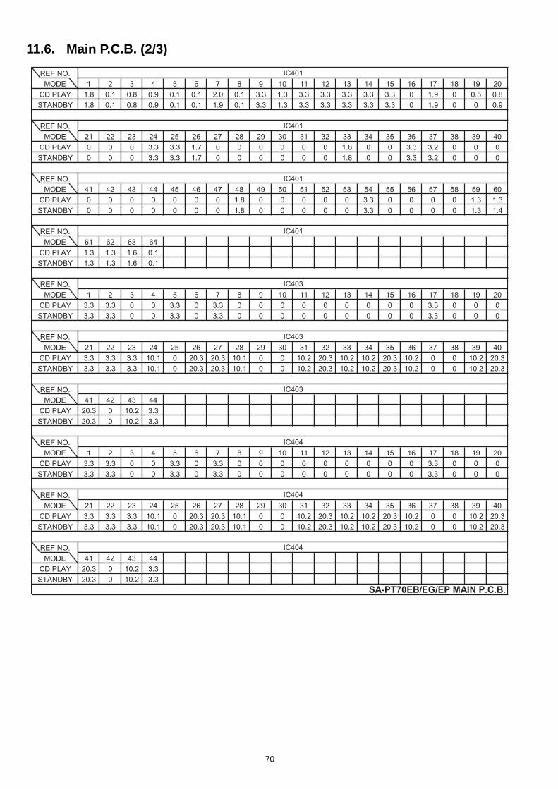
11.6. Main P.C.B. (2/3)
REF NO.MODE 1 2 3 4 5 6 7 8 9 10 11 12 13 14 15 16 17 18 19 20
CD PLAY 1.8 0.1 0.8 0.9 0.1 0.1 2.0 0.1 3.3 1.3 3.3 3.3 3.3 3.3 3.3 0 1.9 0 0.5 0.8STANDBY 1.8 0.1 0.8 0.9 0.1 0.1 1.9 0.1 3.3 1.3 3.3 3.3 3.3 3.3 3.3 0 1.9 0 0 0.9
REF NO.MODE 21 22 23 24 25 26 27 28 29 30 31 32 33 34 35 36 37 38 39 40
CD PLAY 0 0 0 3.3 3.3 1.7 0 0 0 0 0 0 1.8 0 0 3.3 3.2 0 0 0STANDBY 0 0 0 3.3 3.3 1.7 0 0 0 0 0 0 1.8 0 0 3.3 3.2 0 0 0
REF NO.MODE 41 42 43 44 45 46 47 48 49 50 51 52 53 54 55 56 57 58 59 60
CD PLAY 0 0 0 0 0 0 0 1.8 0 0 0 0 0 3.3 0 0 0 0 1.3 1.3STANDBY 0 0 0 0 0 0 0 1.8 0 0 0 0 0 3.3 0 0 0 0 1.3 1.4
REF NO.MODE 61 62 63 64
CD PLAY 1.3 1.3 1.6 0.1STANDBY 1.3 1.3 1.6 0.1
REF NO.MODE 1 2 3 4 5 6 7 8 9 10 11 12 13 14 15 16 17 18 19 20
CD PLAY 3.3 3.3 0 0 3.3 0 3.3 0 0 0 0 0 0 0 0 0 3.3 0 0 0STANDBY 3.3 3.3 0 0 3.3 0 3.3 0 0 0 0 0 0 0 0 0 3.3 0 0 0
REF NO.MODE 21 22 23 24 25 26 27 28 29 30 31 32 33 34 35 36 37 38 39 40
CD PLAY 3.3 3.3 3.3 10.1 0 20.3 20.3 10.1 0 0 10.2 20.3 10.2 10.2 20.3 10.2 0 0 10.2 20.3STANDBY 3.3 3.3 3.3 10.1 0 20.3 20.3 10.1 0 0 10.2 20.3 10.2 10.2 20.3 10.2 0 0 10.2 20.3
REF NO.MODE 41 42 43 44
CD PLAY 20.3 0 10.2 3.3STANDBY 20.3 0 10.2 3.3
IC404
SA-PT70EB/EG/EP MAIN P.C.B.
IC401
IC404
IC403
IC403
IC404
IC401
IC401
IC401
IC403
70
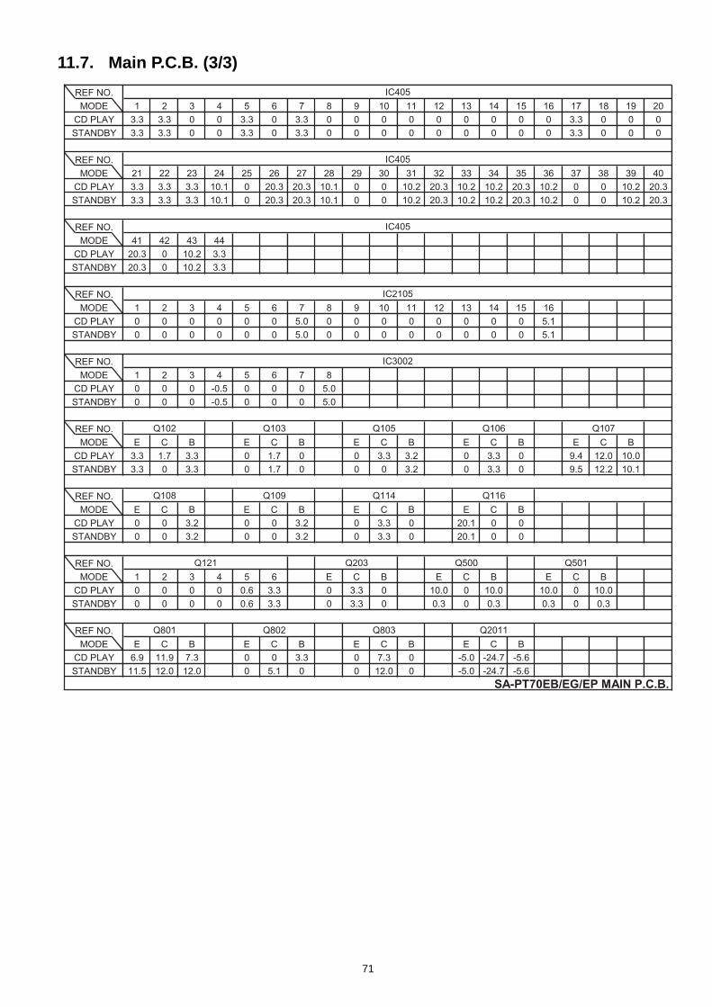
11.7. Main P.C.B. (3/3)
REF NO.MODE 1 2 3 4 5 6 7 8 9 10 11 12 13 14 15 16 17 18 19 20
CD PLAY 3.3 3.3 0 0 3.3 0 3.3 0 0 0 0 0 0 0 0 0 3.3 0 0 0STANDBY 3.3 3.3 0 0 3.3 0 3.3 0 0 0 0 0 0 0 0 0 3.3 0 0 0
REF NO.MODE 21 22 23 24 25 26 27 28 29 30 31 32 33 34 35 36 37 38 39 40
CD PLAY 3.3 3.3 3.3 10.1 0 20.3 20.3 10.1 0 0 10.2 20.3 10.2 10.2 20.3 10.2 0 0 10.2 20.3STANDBY 3.3 3.3 3.3 10.1 0 20.3 20.3 10.1 0 0 10.2 20.3 10.2 10.2 20.3 10.2 0 0 10.2 20.3
REF NO.MODE 41 42 43 44
CD PLAY 20.3 0 10.2 3.3STANDBY 20.3 0 10.2 3.3
REF NO.MODE 1 2 3 4 5 6 7 8 9 10 11 12 13 14 15 16
CD PLAY 0 0 0 0 0 0 5.0 0 0 0 0 0 0 0 0 5.1STANDBY 0 0 0 0 0 0 5.0 0 0 0 0 0 0 0 0 5.1
REF NO.MODE 1 2 3 4 5 6 7 8
CD PLAY 0 0 0 -0.5 0 0 0 5.0STANDBY 0 0 0 -0.5 0 0 0 5.0
REF NO.MODE E C B E C B E C B E C B E C B
CD PLAY 3.3 1.7 3.3 0 1.7 0 0 3.3 3.2 0 3.3 0 9.4 12.0 10.0STANDBY 3.3 0 3.3 0 1.7 0 0 0 3.2 0 3.3 0 9.5 12.2 10.1
REF NO.MODE E C B E C B E C B E C B
CD PLAY 0 0 3.2 0 0 3.2 0 3.3 0 20.1 0 0STANDBY 0 0 3.2 0 0 3.2 0 3.3 0 20.1 0 0
REF NO.MODE 1 2 3 4 5 6 E C B E C B E C B
CD PLAY 0 0 0 0 0.6 3.3 0 3.3 0 10.0 0 10.0 10.0 0 10.0STANDBY 0 0 0 0 0.6 3.3 0 3.3 0 0.3 0 0.3 0.3 0 0.3
REF NO.MODE E C B E C B E C B E C B
CD PLAY 6.9 11.9 7.3 0 0 3.3 0 7.3 0 -5.0 -24.7 -5.6STANDBY 11.5 12.0 12.0 0 5.1 0 0 12.0 0 -5.0 -24.7 -5.6
Q801 Q802 Q803
Q107
IC3002
Q121 Q203 Q500 Q501
Q106
Q108 Q109 Q114 Q116
IC405
IC405
IC405
SA-PT70EB/EG/EP MAIN P.C.B.
Q2011
IC2105
Q102 Q103 Q105
71
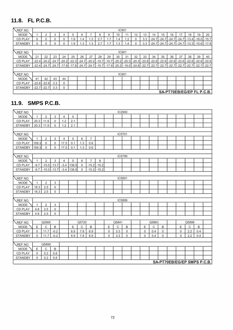
11.8. FL P.C.B.
11.9. SMPS P.C.B.
REF NO.MODE 1 2 3 4 5 6 7 8 9 10 11 12 13 14 15 16 17 18 19 20
CD PLAY 0 0 0 0 1.9 1.4 1.3 2.7 1.7 1.4 1.2 0 3.3 -24.7 -24.7 -24.7 -24.7 -13.4 -18.0 -15.7STANDBY 0 0 0 0 1.9 1.3 1.3 2.7 1.7 1.3 1.4 0 3.3 -24.7 -24.7 -24.7 -24.7 -13.3 -15.6 -17.8
REF NO.MODE 21 22 23 24 25 26 27 28 29 30 31 32 33 34 35 36 37 38 39 40
CD PLAY -22.4 -20.2 -24.7 -20.2 -22.3 -24.7 -20.2 -15.7 -15.7 -25.2 -20.3 -20.3 -22.6 -22.6 -22.6 -22.6 -22.6 -22.6 -22.6 -22.6STANDBY -22.4 -24.7 -24.7 -17.8 -17.8 -24.7 -24.7 -15.7 -17.9 -25.2 -19.0 -24.8 -22.7 -22.7 -22.7 -22.7 -22.7 -22.7 -22.7 -22.7
REF NO.MODE 41 42 43 44
CD PLAY -22.6 -22.6 3.3 0STANDBY -22.7 -22.7 3.3 0
IC901
IC901
IC901
SA-PT70EB/EG/EP FL P.C.B.
REF NO.MODE 1 2 3 4 5
CD PLAY 20.3 11.9 0 1.2 2.1STANDBY 20.3 11.9 0 1.2 2.1
REF NO.MODE 1 2 3 4 5 6 7
CD PLAY 159.3 0 0 17.5 0.1 1.3 0.6STANDBY 159.3 0 0 17.5 0.1 1.3 0.6
REF NO.MODE 1 2 3 4 5 6 7 8
CD PLAY -9.7 -15.0 -13.7 -3.4 138.5 0 -15.2 -15.2STANDBY -9.7 -15.0 -13.7 -3.4 138.5 0 -15.2 -15.2
REF NO.MODE 1 2 3
CD PLAY 18.3 2.5 0STANDBY 18.3 2.5 0
REF NO.MODE 1 2 3
CD PLAY 4.8 2.5 0STANDBY 4.8 2.5 0
REF NO.MODE E C B E C B E C B E C B E C B
CD PLAY 0 11.7 -0.2 6.9 7.8 6.9 0 3.3 0 0 0.4 0 0 2.2 0.4STANDBY 0 11.7 -0.2 6.9 7.8 6.9 0 3.3 0 0 0.4 0 0 2.2 0.4
REF NO.MODE E C B
CD PLAY 0 0.2 0.8STANDBY 0 0.2 0.8
IC2900
IC5701
IC5799
Q2900 Q5720 Q5841
IC5801
IC5899
Q5863 Q5898
Q5899
SA-PT70EB/EG/EP SMPS P.C.B.
72
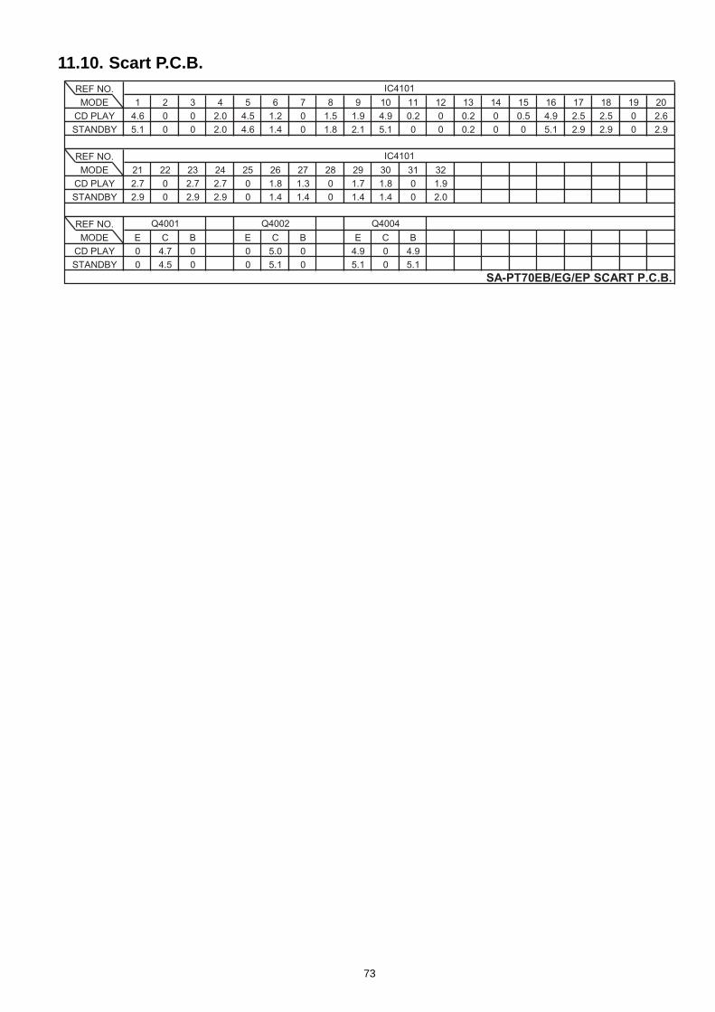
11.10. Scart P.C.B.REF NO.MODE 1 2 3 4 5 6 7 8 9 10 11 12 13 14 15 16 17 18 19 20
CD PLAY 4.6 0 0 2.0 4.5 1.2 0 1.5 1.9 4.9 0.2 0 0.2 0 0.5 4.9 2.5 2.5 0 2.6STANDBY 5.1 0 0 2.0 4.6 1.4 0 1.8 2.1 5.1 0 0 0.2 0 0 5.1 2.9 2.9 0 2.9
REF NO.MODE 21 22 23 24 25 26 27 28 29 30 31 32
CD PLAY 2.7 0 2.7 2.7 0 1.8 1.3 0 1.7 1.8 0 1.9STANDBY 2.9 0 2.9 2.9 0 1.4 1.4 0 1.4 1.4 0 2.0
REF NO.MODE E C B E C B E C B
CD PLAY 0 4.7 0 0 5.0 0 4.9 0 4.9STANDBY 0 4.5 0 0 5.1 0 5.1 0 5.1
IC4101
IC4101
SA-PT70EB/EG/EP SCART P.C.B.
Q4001 Q4002 Q4004
73
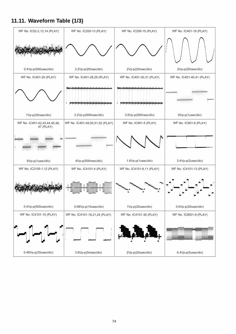
11.11. Waveform Table (1/3)
WF No. IC52-2,13,14 (PLAY)
0.4Vp-p(500usec/div)
WF No. IC200-13 (PLAY)
3.2Vp-p(20nsec/div)
WF No. IC200-15 (PLAY)
2Vp-p(20nsec/div)
WF No. IC401-19 (PLAY)
2Vp-p(20nsec/div)
WF No. IC401-20 (PLAY)
1Vp-p(20nsec/div)
WF No. IC401-42,43,44,45,46, 47 (PLAY)
6Vp-p(1usec/div)
WF No. IC401-28,29 (PLAY)
3.2Vp-p(500nsec/div)
WF No. IC401-49,50,51,52 (PLAY)
6Vp-p(500nsec/div)
WF No. IC401-30,31 (PLAY)
3.6Vp-p(500nsec/div)
WF No. IC901-5 (PLAY)
1.6Vp-p(1usec/div)
WF No. IC4101-4 (PLAY)
0.68Vp-p(10usec/div)
WF No. IC4101-18,21,24 (PLAY)
3.8Vp-p(5msec/div)
WF No. IC4101-30 (PLAY)
2Vp-p(20usec/div)
WF No. IC2105-1,12 (PLAY)
0.4Vp-p(500usec/div)
WF No. IC8001-9 (PLAY)
6.4Vp-p(5usec/div)
WF No. IC4101-13 (PLAY)
0.6Vp-p(20usec/div)
WF No. IC4101-15 (PLAY)
0.48Vp-p(20usec/div)
WF No. IC401-40,41 (PLAY)
6Vp-p(1usec/div)
WF No. IC901-8 (PLAY)
3.4Vp-p(2usec/div)
WF No. IC4101-8,11 (PLAY)
1Vp-p(20usec/div)
74
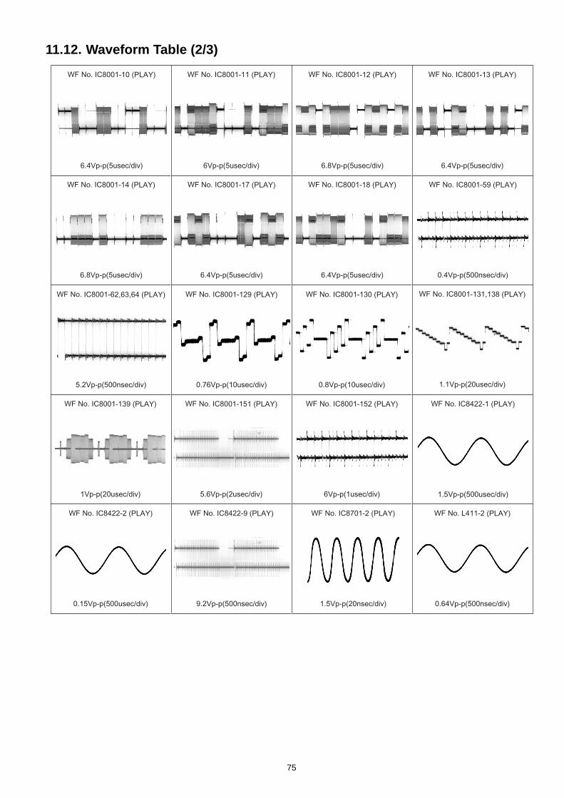
11.12. Waveform Table (2/3)
WF No. IC8001-10 (PLAY)
6.4Vp-p(5usec/div)
WF No. IC8001-14 (PLAY)
6.8Vp-p(5usec/div)
WF No. IC8001-62,63,64 (PLAY)
5.2Vp-p(500nsec/div)
WF No. IC8001-17 (PLAY)
6.4Vp-p(5usec/div)
WF No. IC8001-129 (PLAY)
0.76Vp-p(10usec/div)
WF No. IC8001-130 (PLAY)
0.8Vp-p(10usec/div)
WF No. IC8001-131,138 (PLAY)
1.1Vp-p(20usec/div)
WF No. IC8001-18 (PLAY)
6.4Vp-p(5usec/div)
WF No. IC8001-59 (PLAY)
0.4Vp-p(500nsec/div)
WF No. IC8001-11 (PLAY)
6Vp-p(5usec/div)
WF No. IC8001-12 (PLAY)
6.8Vp-p(5usec/div)
WF No. IC8001-13 (PLAY)
6.4Vp-p(5usec/div)
WF No. IC8001-139 (PLAY)
1Vp-p(20usec/div)
WF No. IC8001-151 (PLAY)
5.6Vp-p(2usec/div)
WF No. IC8001-152 (PLAY)
6Vp-p(1usec/div)
WF No. IC8422-1 (PLAY)
1.5Vp-p(500usec/div)
WF No. IC8422-2 (PLAY)
0.15Vp-p(500usec/div)
WF No. IC8422-9 (PLAY)
9.2Vp-p(500nsec/div)
WF No. IC8701-2 (PLAY)
1.5Vp-p(20nsec/div)
WF No. L411-2 (PLAY)
0.64Vp-p(500nsec/div)
75
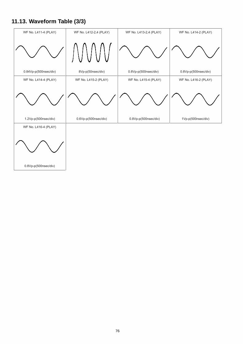
11.13. Waveform Table (3/3)
WF No. L411-4 (PLAY)
0.84Vp-p(500nsec/div)
WF No. L412-2,4 (PLAY)
8Vp-p(50nsec/div)
WF No. L413-2,4 (PLAY)
0.8Vp-p(500nsec/div)
WF No. L414-2 (PLAY)
0.8Vp-p(500nsec/div)
WF No. L414-4 (PLAY)
1.2Vp-p(500nsec/div)
WF No. L415-2 (PLAY)
0.6Vp-p(500nsec/div)
WF No. L415-4 (PLAY)
0.8Vp-p(500nsec/div)
WF No. L416-2 (PLAY)
1Vp-p(500nsec/div)
WF No. L416-4 (PLAY)
0.8Vp-p(500nsec/div)
76
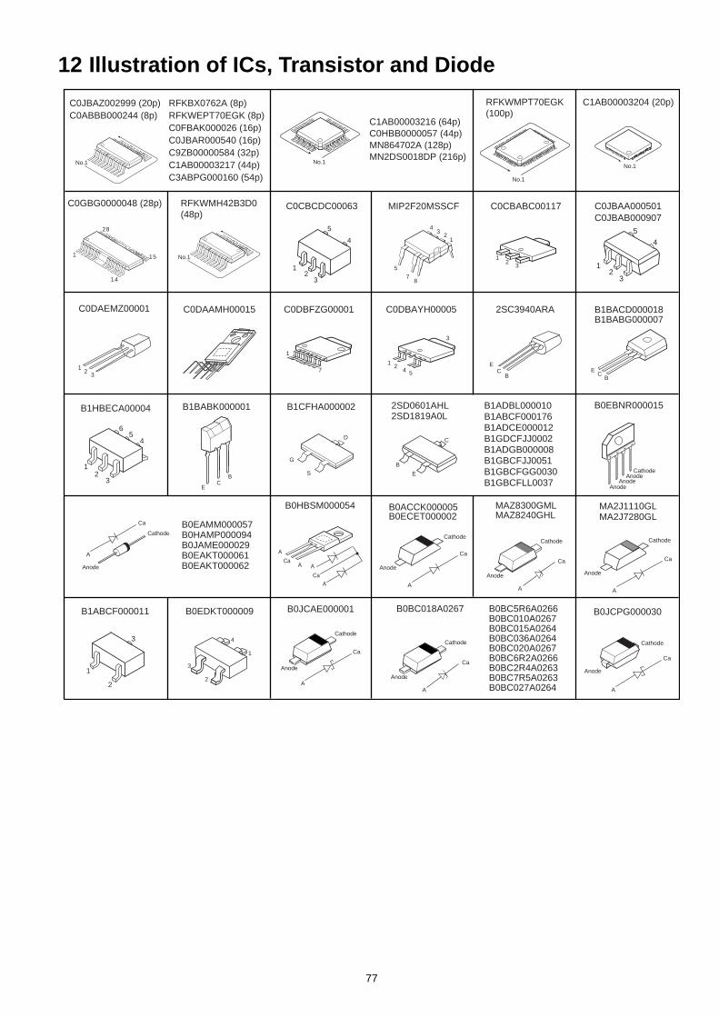
12 Illustration of ICs, Transistor and Diode
A
Ca
Cathode
Anode
A
Ca
Cathode
Anode
A
Ca
Cathode
Anode
AnodeAnode
AnodeCathode
A
Ca
Cathode
Anode
A
Ca
Cathode
AnodeA
Ca
Cathode
Anode
2
3
1
4
Ca
A
A
Ca
A
A
1
42
5
3
No.1
No.1
No.1
No.1
1
4
5
23 8
4
5
7
12
3
1
32
1
7
1
28
15
14
1
4
5
23
E
C
B
BC
E
1
4
65
23
1
3
2
EC
BS
D
G
EC
B
12
3
No.1
B0ACCK000005B0ECET000002
B0BC7R5A0263
B0BC5R6A0266B0BC018A0267B0BC010A0267B0BC015A0264B0BC036A0264B0BC020A0267B0BC6R2A0266B0BC2R4A0263
B0BC027A0264
B0JCAE000001
B0EBNR000015
MAZ8240GHLMA2J1110GLMA2J7280GL
MAZ8300GML
B0JAME000029
B0EAMM000057B0HAMP000094
B0EAKT000062B0EAKT000061
B0EDKT000009
B0HBSM000054
C0DBAYH00005
C0CBABC00117
RFKWMPT70EGK
(100p)
C0CBCDC00063
C0DAAMH00015
MIP2F20MSSCF
C0DAEMZ00001 C0DBFZG00001
C0GBG0000048 (28p)
C0JBAB000907
C0JBAA000501
MN864702A (128p)
MN2DS0018DP (216p)
C1AB00003216 (64p)
C0HBB0000057 (44p)
B1ADCE000012B1ABCF000176
B1GBCFJJ0051
B1BACD000018B1BABG000007
B1ADBL000010B1HBECA00004
B1ABCF000011
B1GBCFLL0037
B1BABK000001 B1CFHA000002
B1GBCFGG0030
B1ADGB000008
C0JBAR000540 (16p)
C1AB00003217 (44p)
C9ZB00000584 (32p)
C3ABPG000160 (54p)
C0FBAK000026 (16p)
C1AB00003204 (20p)
RFKWMH42B3D0
(48p)
RFKBX0762A (8p)C0JBAZ002999 (20p)
RFKWEPT70EGK (8p)C0ABBB000244 (8p)
B1GDCFJJ0002
2SD0601AHL2SD1819A0L
2SC3940ARA
A
Ca
Cathode
Anode
B0JCPG000030
77

78
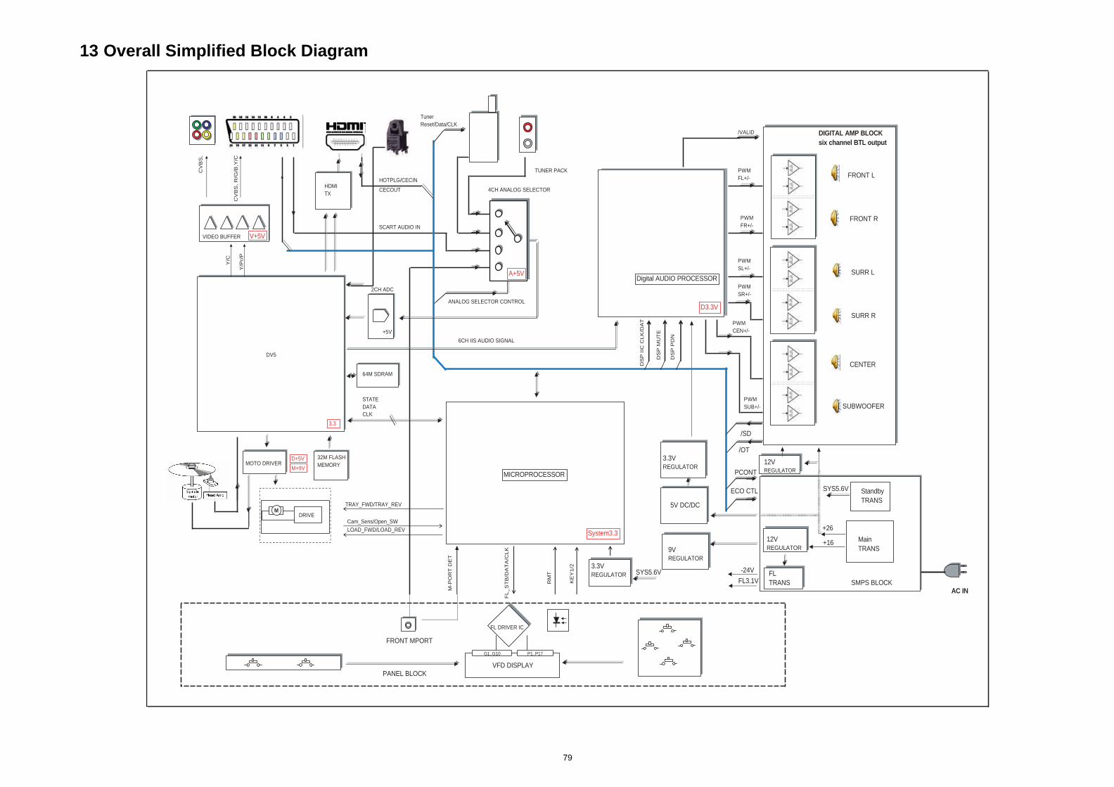
79
13 Overall Simplified Block Diagram
7
Y/C
Y/P
r/P
RM
T
KE
Y1
/2
DS
P P
DN
FRONT L
FRONT R
SURR L
SURR R
CENTER
SUBWOOFER
TUNER PACK
Tuner
Reset/Data/CLK
Standby
TRANS
SYS5.6V
Main
TRANS
+26
+16
-24V
FL3.1V
DV5
CV
BS
,
+5V
System3.3
ESSOR
Digital AUDIO PROCESSOR
DIGITAL AMP BLOCK
six channel BTL output
SMPS BLOCK
HOTPLG/CECIN
CECOUT
AC IN
DS
P M
UT
E
DS
P I
IC C
LK
/DA
T
2CH ADC
6CH IIS AUDIO SIGNAL
ANALOG SELECTOR CONTROL
4CH ANALOG SELECTOR
/VALID
/SD
/OT
PCONT
ECO CTL
SCART AUDIO IN
CV
BS
, R
/G/B
,Y/C
PWM
FL+/-
PWM
FR+/-
PWM
SL+/-
PWM
SR+/-
PWM
CEN+/-
PWM
SUB+/-
5V DC/DC
9VREGULATOR
12VREGULATOR
3.3VREGULATOR
FL
TRANS
D3.3V
A+5V
V+5V
3.3VREGULATOR
12VREGULATOR
SYS5.6V
VIDEO BUFFER
HDMI
TX
G1..G10 P1..P1
MDRIVE
TRAY_FWD/TRAY_REV
Cam_Sens/Open_SW
LOAD_FWD/LOAD_REV
FL
_S
TB
/DA
TA
/CL
K
MICROPROC
VFD DISPLAYPANEL BLOCK
FRONT MPORT
FL DRIVER IC
STATE
DATA
CLK
64M SDRAM
32M FLASH
MEMORY
3.3
M-P
OR
T D
ET
MOTO DRIVERM+9V
D+5V
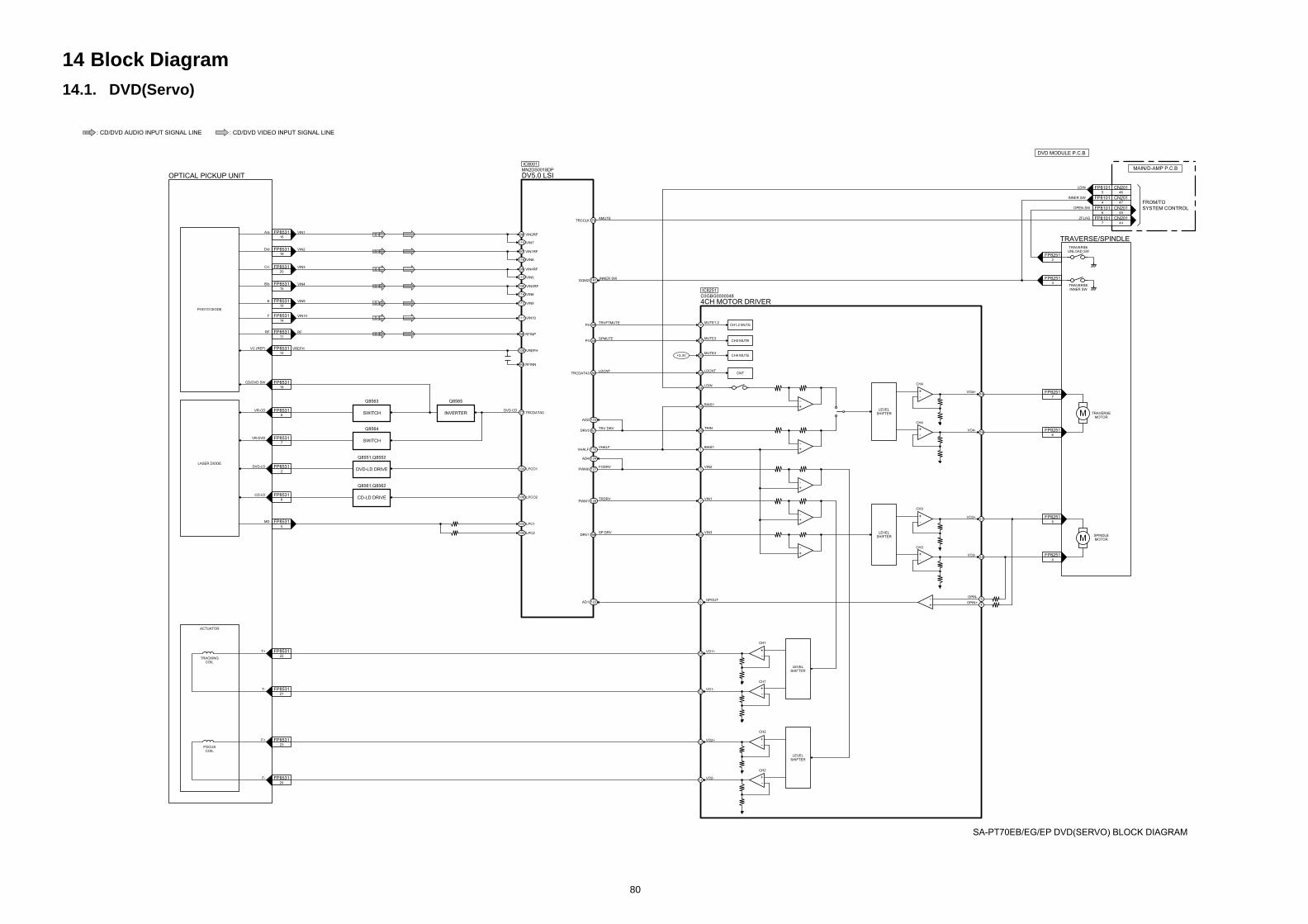
80
14 Block Diagram14.1. DVD(Servo)
SA-PT70EB/EG/EP DVD(SERVO) BLOCK DIAGRAM
: CD/DVD VIDEO INPUT SIGNAL LINE: CD/DVD AUDIO INPUT SIGNAL LINE
FROM/TO
SYSTEM CONTROL
M
M
Q8565
INVERTER
Q8563
SWITCH
+
-
-
+
DV5.0 LSIOPTICAL PICKUP UNIT
TRAVERSE/SPINDLE
MN2DS0018DP
IC8001
4CH MOTOR DRIVERC0GBG0000048
IC8251
A/a VIN1
P4 49
TRCCLK 76
AD2 123
DQM2 191
100
TRVFTMUTE
AMUTE
INNER SW
98 VIN2RF
D/d VIN297 VIN1RF
C/c
PHOTO DIODE
CH1,2 MUTE
TRAVERSEMOTOR
TRAVERSEINNER SW
SPINDLEMOTOR
VIN399 VIN4RF
95 RFINN
77 TRCDATA0
B/b VIN4VIN3RF
115 VIN7
116 VIN8
113 VIN5
114 VIN6
112 VIN9
111 VIN10
E VIN9
F VIN10
RF RF96 RFINP
9MUTE1,2
TRCDATA3
VO4+
CH4
CH4
CH3
CH3
VO4-
VO3+
VO3-
80LDCNT
V
CNT
LEVELSHIFTER
LEVELSHIFTER
28LDCNT
26TRIN
1BIAS1
+
-
24LDIN
25
15
-
+16
-
+17
-
+
-
+
18
OPIN-5
OPIN+4
CH1
CH1
VO1+
VO1-
LEVELSHIFTER
-
+14
OPOUT6
-
+13
CH2
CH2
VO2+
VO2-
LEVELSHIFTER
-
+12
-
+11
BIAS1
+
-
3VIN2
+
-
2VIN1
+
-
23VIN3
P3 48SPMUTE
CH3 MUTE27MUTE3
CH4 MUTE20MUTE4
16
FP8531
19
FP8531
20
FP8531
15
FP8531
10
FP8531
14
FP8531
109 VREFHVC (REF) VREFH
12
FP8531
CD/DVD SW
DVD CD
OPEN SW
INNER SW
18
FP8531
VR-CD
8
FP8531
17
FP8531
4
FP8251
5
FP8251
7
FP8251
3
FP8251
TRAVERSEUNLOAD SW
2
FP8251
6
FP8251
+3.3V
474
CN201FP8101
LDIN
465
CN201FP8101
456
CN201FP8101
ZFLAG
447
CN201FP8101
MAIN/D-AMP P.C.B
DVD MODULE P.C.B
Q8564
SWITCH
AD4 124
PWM0 127
PWM1 126
VHALF 110
LASER DIODE
ACTUATOR
TRACKINGCOIL
DRV0 67
DRV1 66
TRV DR
VHALF
FODRV
SP DRV
TRDRV
AD1 122
104 LPCO1
103 LPC1
105 LPC2
VR-DVD
7
FP8531
Q8551,Q8552
DVD-LD DRIVEDVD-LD
2
FP8531
106 LPCO2
Q8561,Q8562
CD-LD DRIVECD-LD
6
FP8531
T+
22
FP8531
T-
21
FP8531
FOCUSCOIL
F+
23
FP8531
F-
24
FP8531
MD
5
FP8531
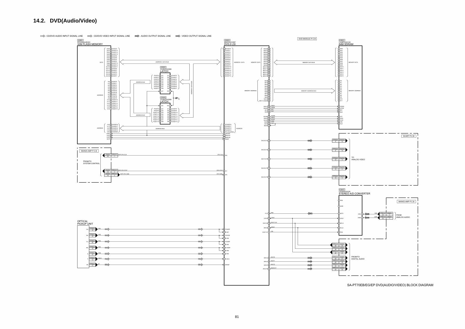
81
14.2. DVD(Audio/Video)
SA-PT70EB/EG/EP DVD(AUDIO/VIDEO) BLOCK DIAGRAM
DV5.0 LSIMN2DS0018DP
IC8001
42
41
40
39
38
37
36
29
28
27
26
25
24
23
22
160
162
164
168
170
172
176
178
177
175
171
169
167
163
161
159
EXADT0212
NEXCE212
NEXOE214
DATA
45DQ15
DQ14 43
41DQ13
DQ12 39
36DQ11
DQ10 34
32DQ9
DQ8 30
DQ7 44
DQ6 42
DQ5 40
38DQ4
DQ3 35
33DQ2
31DQ1
DQ0
EXADT1
EXADT3
EXADT5
EXADT7
EXADT9
10A20
A19 9
16A18
A17 17
48A16
RST 12
28XOE
XCE 26
11XWE
EXADR20
EXADR19
EXADR18
EXADR17
EXADR16
EXADT11
EXADT13
EXADT15
EXADT2
EXADT4
EXADT6
EXADT8
EXADT10
EXADT12
EXADT14
EXADT029
ADDRESS
1A15
A14 2
3A13
A12 4
5A11
A10 6
7A9
A8 8
18A7
A6 19
20A5
A4 21
22A3
A2 23
24A1
A0
FEXDT15
FEXDT14
FEXDT13
FEXDT12
FEXDT11
FEXDT10
FEXDT9
FEXDT8
FEXDT7
FEXDT6
FEXDT5
FEXDT4
FEXDT3
FEXDT2
FEXDT1
FEXDT025
ADDRESS
D8 9
D7
D6
8
7
D5
D4
6
5
D3
D2
4
3
D1
EXADT7
EXADT6
EXADT5
EXADT4
EXADT3
EXADT2
EXADT1
EXADT0
FEXDT7
FEXDT6
FEXDT5
FEXDT4
FEXDT3
FEXDT2
FEXDT1
FEXDT0 2
12
13
14
15
16
17
18
19
Q8
OE 111 LE
Q7
Q6
Q5
Q4
Q3
Q2
Q1
ADDRESS / DATAADDRESS / DATA BUS
ADDRESS BUS
ADDRESS BUS
ADDRESS BUS
AD
DR
ES
S / D
AT
A B
US
ADDRESS
EXADT15
EXADT14
EXADT13
EXADT12
EXADT11
21
35
34
30
45 P0 (EXADR20)
EXADR19
EXADR18
EXADR17
EXADR16
31 NEXWE
P8
P6
70 NRST
EXADT10
EXADT9
EXADT8
EXADT7
EXADT6
EXADT5
EXADT4
EXADT3
EXADT2
EXADT1
64M SDRAMC3ABPG000160
IC8051
4
5
7
8
10
11
13
42
44
45
47
48
50
51
53
MEMORY DATA
MEMORY ADDRESS
DQ15
DQ14
DQ13
DQ12
DQ11
DQ10
DQ9
DQ8
DQ7
DQ6
DQ5
DQ4
DQ3
DQ2
DQ1
2 DQ0
24
25
26
29
30
31
32
33
34
22
35 A11
A10
A9
A8
A7
A6
A5
A4
A3
A2
A1
23 A0
32M FLASH MEMORYRFKWMH42B3D0
IC8651
LATCHC0JBAZ002999
IC9001
D8 9
D7
D6
8
7
D5
D4
6
5
D3
D2
4
3
D1
EXADT15
EXADT14
EXADT13
EXADT12
EXADT11
EXADT10
EXADT9
EXADT8
FEXDT15
FEXDT14
FEXDT13
FEXDT12
FEXDT11
FEXDT10
FEXDT9
FEXDT8 2
12
13
14
15
16
17
18
19
Q8
OE 111 LE
Q7
Q6
Q5
Q4
Q3
Q2
Q1
LATCHC0JBAZ002999
IC9002
MEMORY ADDRESS
MEMORY DATA MEMORY DATA BUS
MEMORY ADDRESS BUS
MDQ15
MDQ14
MDQ13
MDQ12
MDQ11
MDQ10
MDQ9
MDQ8
MDQ7
MDQ6
MDQ5
MDQ4
MDQ3
MDQ2
MDQ1
MDQ0
201
203
207
209
208
206
202
200
198
194
199
192(MA11) DQM3
MA10
MA9
MA8
MA7
19
18
17
16
38 CLK
/WE
/CAS
/RAS
/CS
CLK
NWE
NCAS
NRAS
NCSM190
189
188
181
183MCK
185MCKI
NWE
NCAS
NRAS
NCSM
39
15
21
20 BA0
BA1
LDQM
UDQM
BA0
BA1
DMQ0
DMQ1180
179
197
193BA0
BA1
DMQ0
DMQ1
MA6
MA5
MA4
MA3
MA2
MA1
MA0
P7
MAIN/D-AMP P.C.B
TO
ANALOG VIDEO
DVD MODULE P.C.B
DAC5OUT
DAC4OUT
DAC1OUT
DAC2OUT
DAC3OUT
139
138
131
130
129513
CN4001FP8301
612
CN4001FP8301
126
CN4001FP8301
108
CN4001FP8301
810
CN4001FP8301
SCART P.C.B
VIN2RF
VIN1RF
VIN4RF
VIN3RF
VIN7
VIN8
VIN5
VIN6
VIN9
VIN10
RFINP
48 3
FP8101 CN201
50 1
FP8101 CN201
AINL
AINR
P12 59AIN0
9 SDT0
LRCKLRCK
10 LRCK
ADAC-CLK11 MCLK
SRCK12 SCLK
EXDT10 4
DRV3 64
DRV4 63
DRV5 62
150
DACCK 148
SRCK 149
ADOUT 151
STB13 PDN
2 AINL
1 AINR
2AINL
1AINR
STEREO A/D CONVERTERC0FBAK000026
IC8422
1536
CN201FP8101
AOUT0
2130
CN201FP8101
AOUT1
1932
CN201FP8101
AOUT2
1734
CN201FP8101
DMIXOUT
2625
CN201FP8101
2328
CN201FP8101
2526
CN201FP8101
FROM/TO
DIGITAL AUDIO
FROM
ANALOG AUDIO
MAIN/D-AMP P.C.B
: CD/DVD VIDEO INPUT SIGNAL LINE: CD/DVD AUDIO INPUT SIGNAL LINE : AUDIO OUTPUT SIGNAL LINE : VIDEO OUTPUT SIGNAL LINE
DOP CPU CLK55
CPU CLK
53CPU CMD
150
FP8101CN201
DOP CPU STAT
DOP CPU CMD
54CPU STAT
348
FP8101CN201
249
FP8101CN201
FROM/TO
SYSTEM CONTROL
OPTICALPICKUP UNIT
A/aVIN1
100
98
D/dVIN2
97
C/cVIN3
99
B/bVIN4
115
116
113
114
112
111
EVIN9
FVIN10
RFRF
96
16
FP8531
19
FP8531
20
FP8531
15
FP8531
10
FP8531
14
FP8531
17
FP8531
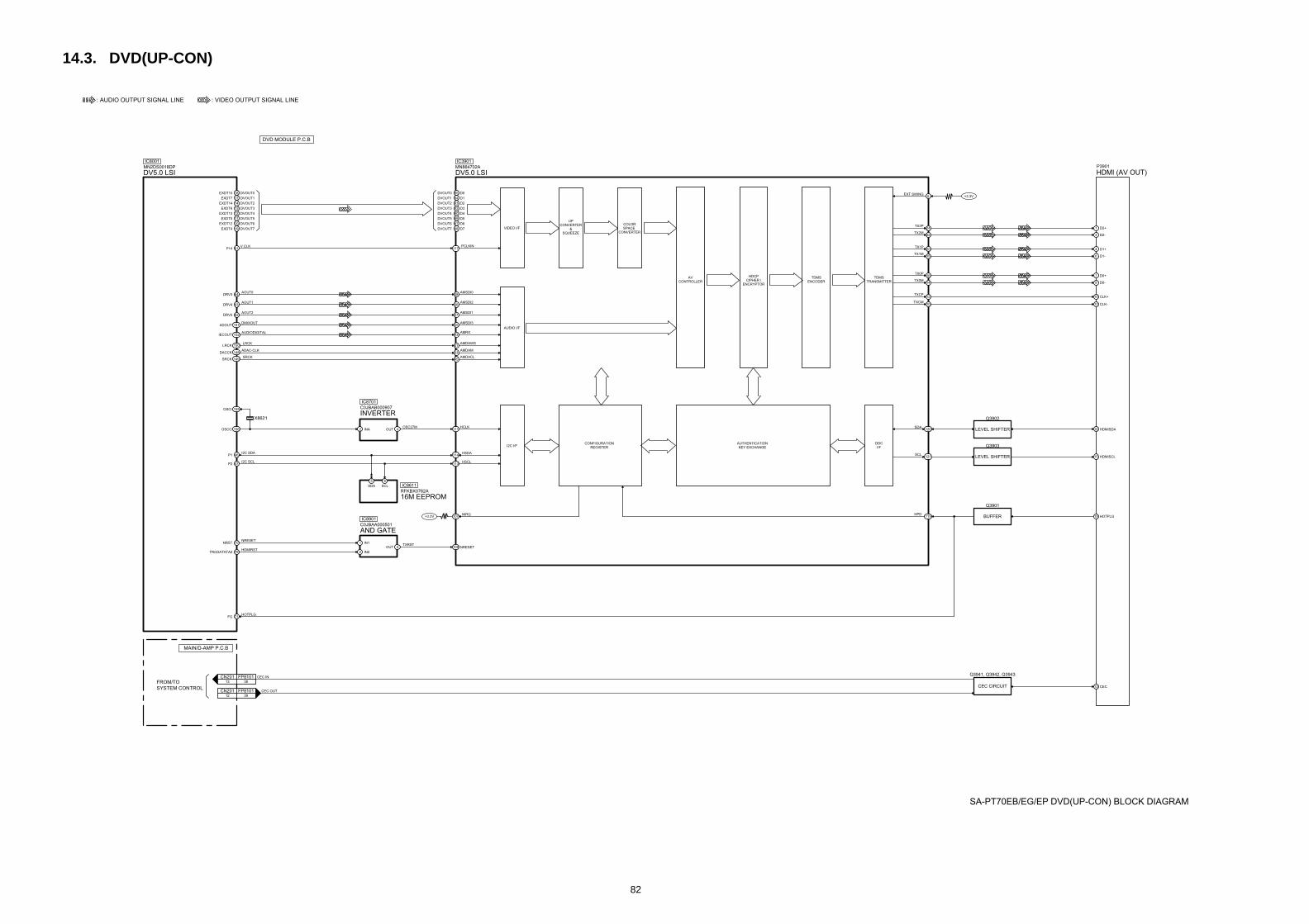
82
14.3. DVD(UP-CON)
SA-PT70EB/EG/EP DVD(UP-CON) BLOCK DIAGRAM
: AUDIO OUTPUT SIGNAL LINE : VIDEO OUTPUT SIGNAL LINE
X8621
+3.3V
HDMI (AV OUT)P3901
Q3902
LEVEL SHIFTER
DV5.0 LSIMN2DS0018DP
IC8001
DV5.0 LSIMN864702A
IC3901
INVERTERC0JBAB000907
IC8701
EXDT15 18 EXT SWING8
TX2P24
TX2M22
TX1P20
TX1M18
TX0P16
TX0M14
TXCP12
TXCM10
DVOUT0
EXDT7 17 DVOUT1
EXDT14 14 DVOUT2
EXDT6 13 DVOUT3
EXDT13 12 DVOUT4
EXDT5 11 DVOUT5
EXDT12 10 DVOUT6
EXDT4 19 DVOUT7
DVOUT0
DVOUT1
DVOUT2
DVOUT3
DVOUT4
DVOUT5
DVOUT6
DVOUT7
P14 61V CLK
95 D0
94 D1
93 D2
92 D3
90 D4
89 D5
87 D6
88 D7
38AMSDI0
36AMSDI2
37AMSDI1
35AMSDI3
41AMDAWS
33AMDAM
45AMDACL
1 D2+
3 D2-
4 D1+
6 D1-
7 D0+
9 D0-
10 CLK+
12 CLK-
16 HDMISDA
PCLKIN
VIDEO I/F
AUDIO I/F
N AUTHENTICATIONKEY EXCHANGE
UPCONVERTER
&SQUEEZE
COLORSPACE
CONVERTER
AVCONTROLLER
HDCPCIPHER /
ENCRYPTOR
TDMSENCODER
TDMSTRANSMITTER
DDCI/F
117
120SDA
Q3901
BUFFER
Q3941, Q3942, Q3943
CEC CIRCUIT
19 HOTPLG
13 CEC
119HPD
Q3903
LEVEL SHIFTER 15 HDMISCL121SCL
LRCKLRCK
ADAC-CLK
SRCK
DRV3 64
DRV4 63
DRV5 62
150
DACCK 148
SRCK 149
OSCI 155
ADOUT 151
AOUT0
AOUT1
AOUT2
DMIXOUT
43AMRX
IECOUT 152AUDIODIGITAL
DVD MODULE P.C.B
+3.3V
AND GATEC0JBAA000501
IC8901
OUT 4
NRESET
2 INA
OUT 4
1 IN1
38
CEC IN
13
FP8101CN201
39
CEC OUT
12
FP8101CN201
I2C I/FCONFIGURATIO
REGISTER
111
114
HCLKOSC27M
TXRST
16M EEPROMRFKBX0762A
IC86115 6
SDA SCL
OSCO 156
HSDA
107NIRQ
P1 46I2C SDA
NRST 70NRESET
FG 71HOTPLG
2 IN2TRCDATATA2 79HDMIRST
113
108
HSCLP2 47
I2C SCL
MAIN/D-AMP P.C.B
FROM/TO
SYSTEM CONTROL
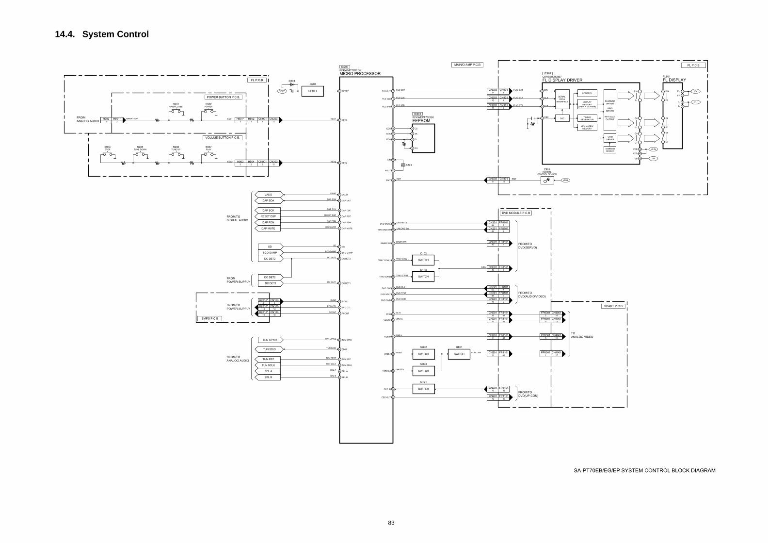
83
14.4. System Control
SA-PT70EB/EG/EP SYSTEM CONTROL BLOCK DIAGRAM
99
CN901CN203
1 CS
2 SK
3 DI
4 DO
MICRO PROCESSORRFKWMPT70EGK
IC200
EEPROMRFKWEPT70EGK
X201
IC201
FL DISPLAY DRIVERC0HBB0000057
IC901
FLD OUT 7 7DINFL IC DAT
810
CN901CN203FLD CLK 6
FL IC CLK
711
CN901CN203
3 2
MPORT SWH902 H901*
FLD STB 5
ECS 78
ECK 77
EDA 76
XIN 15
RESET12
XOUT 13
FL IC STB
108
CN901CN203 RMT
FLD OUT
FLD CLK
FLD STB
LDIN
KEY197KEY1
POWER
KEY1
8CLK
9STB
5
13
43
VDD
VDD
30-VP
OSC
P16
P1
P16
P1
G6
G1
G6
G1
G9
G7
G9
G7
FL901
S902OPEN/CLOSE
S901
FL DISPLAY
SERIAL
DATA
INTERFACE
OSC
CONTROL
DISPLAY
MEMORY(24bits x 12 Words)
SEGMENT
DRIVER
GRID
DRIVER
GRID
DRIVER
KEY SCAN
OUTPUTTIMING
GENERATOR
KEY MATRIXMEMORY
DIMMINGCIRCUIT
+3.3V
-VP
31
32
F+
F+
F+
1
2
F-
F-
F-
VREF
VREF
3 3
H901* H9025 13
CN901 CN203
KEY295KEY2
PLAY
KEY2
S907TUNE UPS906
TUNE DOWNS905
STOPS904
2 2
H903 H9046 12
CN901 CN203
REMOTECONTROL SENSOR
Z901
Q203D203
RESET
DVD MUTE 60DVD MUTE
RMT 18RMT
44 7
CN201 FP8101
INNER SW 57INNER SW
447
FP8101CN201
Q102
SWITCH
UNLOAD SW 56UNLOAD SW
45 6
CN201 FP8101
DVD CLK 26DVD CLK
50 1
CN201 FP8101
DVD STAT 29
DVD CMD 30
DVD STAT
DVD CMD
48 3
CN201 FP8101
TRAY CCW L 58TRAY CCW L
546
FP8101CN201
249
FP8101CN201
Q103
SWITCHTRAY CW H 59TRAY CW H
DAP CLK36DAP SCK
DAP SCK
DAP RST71RESET DSP
RESET DSP
DAP PDN72DAP PDN
DAP PDN
DAP MUTE34DAP MUTE
DAP MUTE
/SD21SD
SD
FROM
ANALOG AUDIO
FROM/TO
DIGITAL AUDIO
DAP DAT35DAP SDA
DAP SDA
VALID75VALID
VALID
FROM/TO
DVD(SERVO)
FROM/TO
DVD(AUDIO/VIDEO)
FROM/TO
DVD(UP-CON)
TO
ANALOG VIDEO
FL P.C.B
FL P.C.B
POWER BUTTON P.C.B.
VOLUME BUTTON P.C.B.
DVD MODULE P.C.B
Q801
SWITCH
Q802
SWITCH
Q803
SWITCH
162
CN4001FP8301
125
CN4001FP8301
153
CN4001FP8301
YC H
VMUTE
RGB H
FUNC SW
171
CN4001FP8301
4110
FP8101CN201
429
FP8101CN201
438
FP8101CN201
4011
FP8101CN201
YC H 54
VMUTE 54
RGB H 51
WIDE1WIDE1 68
VMUTE2VMUTE2 52
SCART P.C.B
MAIN/D-AMP P.C.B
3813
FP8101CN201
3912
FP8101CN201
Q121
BUFFERCEC IN
CEC OUT
74
73
PCONT24PCONT
10 10
H2016* CN103
ECO CTL4ECO CTL
14 14
H2016* CN103
SYNC19SYNC
DC DET125DC DET1
6 6
H2016* CN103
DC DET1
ECO DAMP94ECO DAMP
ECO DAMP
TUN RST37TUN REST
TUN RST
TUN SCLK39TUN SCLK
TUN SCLK
SEL A48SEL A
SEL A
SEL B49SEL B
SEL B
DC DET226DC DET2
DC DET2
TUN GPIO42TUN GP102
TUN GP102
SDIO38TUN SDIO
DC DET2
FROM/TO
POWER SUPPLY
FROM/TO
ANALOG AUDIO
FROM
POWER SUPPLY
TUN SDIO
SMPS P.C.B
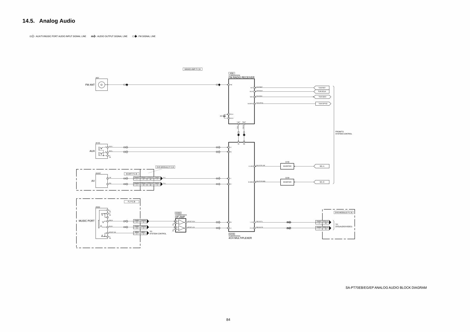
84
14.5. Analog Audio
: AUX/TV/MUSIC PORT AUDIO INPUT SIGNAL LINE : AUDIO OUTPUT SIGNAL LINE : FM SIGNAL LINE
SA-PT70EB/EG/EP ANALOG AUDIO BLOCK DIAGRAM
X51
FM ANT
JK51
Q108
INVERTER
Q109
INVERTER
483
FP8101CN201
501
FP8101CN201
R
L
AUX
JK100
2
3
4CH MULTIPLEXERC0JBAR000540
IC2105
FM RADIO RECEIVERC1AB00003204
IC52
L CH 3
RST 5
SCLK 7
SDIO 8
GCGPO2 18
R CH 13
AUX L
RECOUT-L
TUN REST
TUN SCLK
TUN SDIO
TUN GP102
RECOUT-R
5 L1
A (LSB) 10SELETOR LSB
B (MSB) 9SELETOR MSB
2
1
L0
12
R0
14
LOUT
TU
N L
TU
N R
13
ROUT
L2
2 FMI
AUX L15 R2
17 DCLK
9 RCLK
14 R1
11 R3
4 L3
TO
DVD(AUDIO/VIDEO)
FROM/TO
SYSTEM CONTROL
DVD MODULE P.C.B
MAIN/D-AMP P.C.B
TUN RST
TUN SCLK
SEL A
SEL B
TUN GP102
TUN SDIO
2
31
67
5
AV
MUSIC PORT
JK4001
JK902
TV L
744
CN201FP8101171
FP8301CN4001
817
CN203CN901
1
OP-AMPC0ABBB000244
IC3002
LIN6
TV L
MPORT RCH
MPORT LCH
546
CN201FP8101153
FP8301CN4001RIN
MRCH
2
315
CN203CN901MLCH
MPORT SW
7
6
2
5
3
4
1
+
-
+
-
TO
SYSTEM CONTROL3 2
H902 H901*
DVD MODULE P.C.B
FL P.C.B
SCART P.C.B
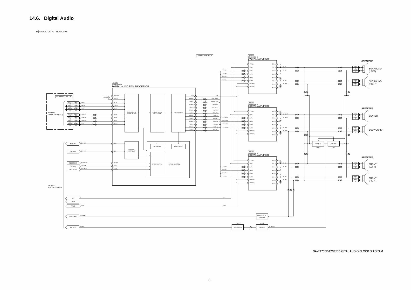
85
14.6. Digital Audio
SA-PT70EB/EG/EP DIGITAL AUDIO BLOCK DIAGRAM
: AUDIO OUTPUT SIGNAL LINE
-
+
-
+
-
+
-
+
-
+
-
+
PWM SECTIONDIGITAL AUDIOPROCESSOR
CLOCK, PLL & SERIAL DATAI/F
PWM M 1 PWM SUBW-
PWM SUBW+
PWM CENT-
PWM CENT+
PWM FR-
PWM FR+
PWM FL-
PWM FL+
PWM SR-
PWM SR+
PWM SL-
PWM SL+
40
VALID VALID
PWM SUBW-
PWM SUBW+
PWM CENT-
PWM CENT+
39
PWM P 141
PWM M 242
PWM P 243
PWM M 344
PWM P 345
PWM M 446
PWM P 447
PWM M 549
PWM P 550
PWM M 651
PWM P 652
2 OTW(L)
5 SD(L)
6 PWM A
8 PWM B
16 PWM C
18 PWM D
7 RST AB(L)
17 RST CD(L)
OUT ASP CENT-
SP CENT+
SP SUB-
SP SUB+
39
BST A 43
OUT B 36
BST B 34
OUT D 28
BST D 24
OUT C 31
BST C 33
DIGITAL AMPLIFIERSPEAKERS
CENTER
SUBWOOFER
C1AB00003217
IC403
PWM SR-
PWM SR+
PWM SL-
PWM SL+
2 OTW(L)
5 SD(L)
6 PWM A
8 PWM B
16 PWM C
18 PWM D
7 RST AB(L)
17 RST CD(L)
OUT ASP SL-
SP SL+
SP SR-
SP SR+
39
BST A 43
OUT B 36
BST B 34
OUT D 28
BST D 24
OUT C 31
BST C 33
DIGITAL AMPLIFIERSPEAKERS
SURROUND
(LEFT)
SURROUND
(RIGHT)
C1AB00003217
IC404
DIGITAL AUDIO PWM PROCESSORC1AB00003216
X400
IC401
PWM FR-
PWM FR+
PWM FL-
PWM FL+
SD
VALID
MCLK63
LRCLK26
SCLK
MCLK
LRCLK
BICK27
XTL OUT19
XTL IN20
2 OTW(L)
5 SD(L)
6 PWM A
8 PWM B
16 PWM C
18 PWM D
7 RST AB(L)
17 RST CD(L)
OUT ASP FL-
SP FL+
SP FR-
SP FR+
SP PROTCT
39
BST A 43
OUT B 36
BST B 34
OUT D 28
BST D 24
OUT C 31
BST C 33
DIGITAL AMPLIFIERSPEAKERS
FRONT
(LEFT)
FRONT
(RIGHT)
C1AB00003217
IC405
1536
CN201FP8101
SDIN131
SDATA0
2130
CN201FP8101
SDIN230
SDATA1
1932
CN201FP8101
SDIN328
SDATA2
1734
CN201FP8101
SDIN429
DMIX
2625
CN201FP8101
2328
CN201FP8101
2526
CN201FP8101
4
JK401
3
JK401
2
JK401
1
JK401
12
JK401
11
JK401
10
JK401
9
JK401
8
JK401
7
JK401
6
JK401
5
JK401
FROM/TO
DVD(AUDIO/VIDEO)
Q500
SWITCH
Q116
SWITCH
ECO SUPLLY
CIRCUIT
Q114
DC DETECT
Q501
SWITCH
DVD MODULE P.C.B
MAIN/D-AMP P.C.B
DEVICE CONTROL
IIC SERIALCONTROL I/F
SYSTEM CONTROL
DAP CONTROL PWM CONTROL
RESET11
SD
RESET DSP
PDN13
DAP PDN
SDA24
DAP SDA
SCL25
DAP SCK
MUTE14
DAP MUTE
VALID
DC DET2
ECO DAMP
FROM/TO
SYSTEM CONTROL
DAP SCK
RESET DSP
SD
ECO DAMP
DC DET2
OTW
DAP PDN
DAP MUTE
DAP SDA
VALID
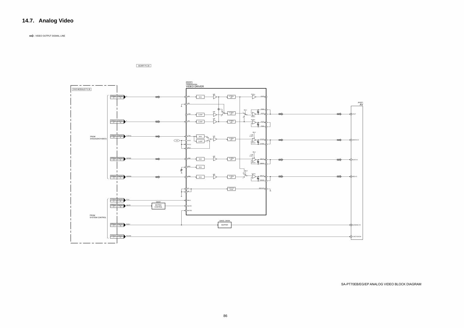
86
14.7. Analog Video
: VIDEO OUTPUT SIGNAL LINE
SA-PT70EB/EG/EP ANALOG VIDEO BLOCK DIAGRAM
COUTCIN
75Ohm6dB
6dB
6.75MHzLPF
13.5MHzLPF
BIAS
6.75MHzLPF
L
L
H
H
L
H
+5V
32
19 VOUT
11 GREEN I/O
7 BLUE I/O
15 RED I/O
8 FUNCTION SW
16 BLANKING I/O
YOUT
75Ohm6.75MHz
LPF 27
YSAG26
CYOUT
75Ohm
L:ONH:OFF
24
CYSAG23
VSAG29
VOUT
75Ohm
SEL3
H
L
SEL3
SEL3
13.5MHzLPF
CBOUT
75Ohm
L:ONH:OFF
21
CBSAG20
SEL3
30
4
13.5MHzLPF
S-DCOUTS1/S2
CROUT
75Ohm
18
SDCOUT18
CRSAG17
SEL7
SEL210
CYINBIAS
CLAMP
11
CVINCLAMP6
6dB
6dB
YINCLAMP8
1
16
VCC1
VCC2
VIDEO DRIVERC9ZB00000584
AVJK4001
Q4002, Q4004
BUFFER
IC4101
C
126
CN4001FP8301
Y
108
CN4001FP8301
CY/PY/G
810
CN4001FP8301
DVD MODULE P.C.B
SCART P.C.B
FROM
DVD(AUDIO/VIDEO)
CBIN
6dB
BIAS13
CRIN
6dB
BIAS15
S12
S23
BIASBIAS9
28 SEL3
5 MUTE1
14 MUTE2
YC H
Q4001
MUTING
CONTROL
162
CN4001FP8301
VMUTE
125
CN4001FP8301
RGB H
153
CN4001FP8301
FUN SW
171
CN4001FP8301
CR/PR/R
513
CN4001FP8301
CB/PB/B
612
CN4001FP8301
FROM
SYSTEM CONTROL
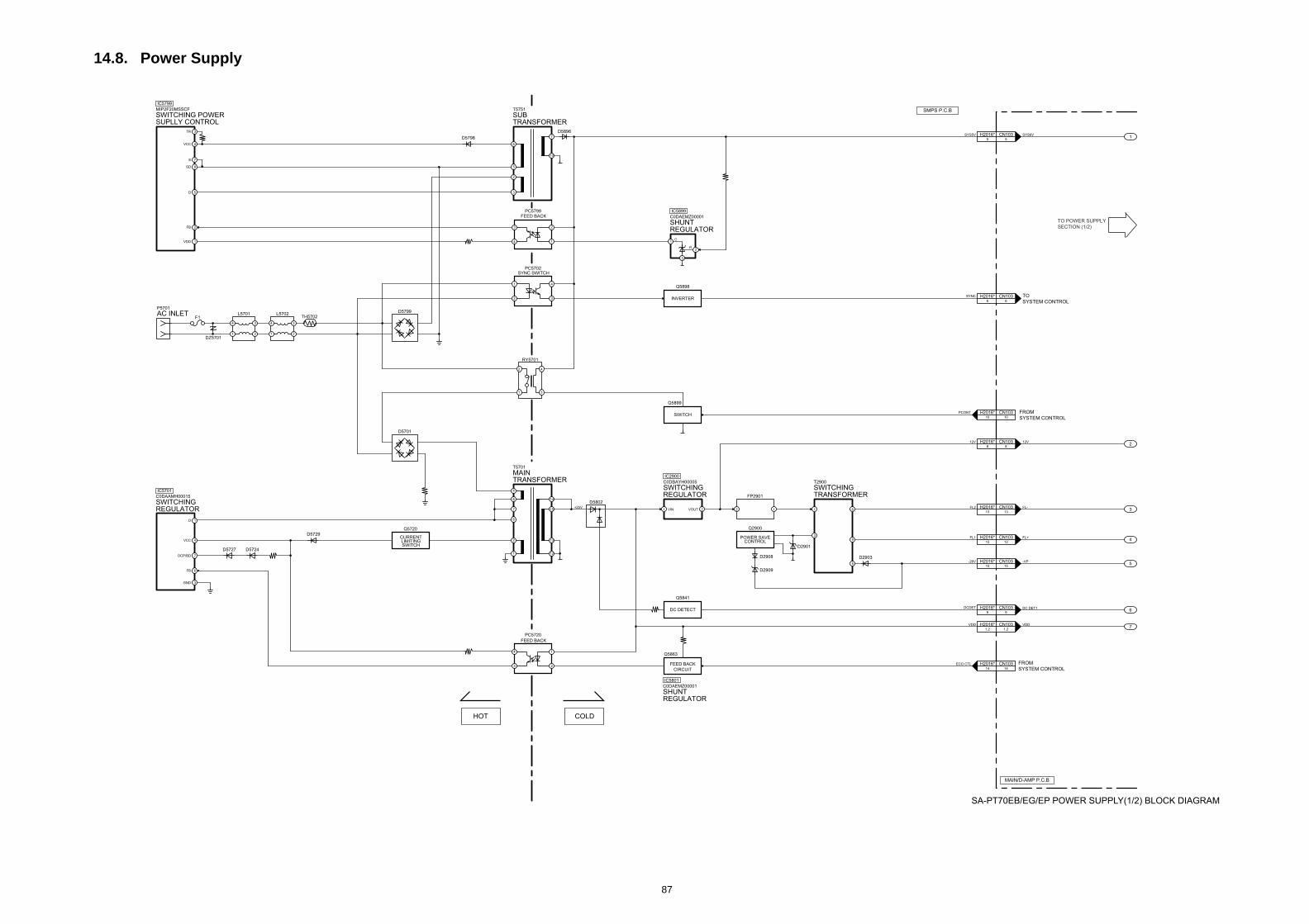
87
14.8. Power Supply
1
2
3
4
5
6
7
SA-PT70EB/EG/EP POWER SUPPLY(1/2) BLOCK DIAGRAM
TO POWER SUPPLY
SECTION (1/2)
AC INLETP5701
F1
DZ5701
L5701
1,21,2
CN103H2016*
1414
CN103H2016*
99
CN103H2016*
66
CN103H2016*
1010
CN103H2016*
VDDVDD
55
CN103H2016* SYS6VSYS5V
88
CN103H2016* 12V12V
1212
CN103H2016* FL+FL1
1313
CN103H2016* FL-FL2
1515
CN103H2016* -VP
DC DET1
-26V
SD 8
S 7
FB 2
VDD 1
D 5
1C
SHUNTREGULATOR
C0DAEMZ00001
IC5899
SWITCHING POWERSUPLLY CONTROL
MIP2F20MSSCF
IC5799
R2
3
SHUNTREGULATOR
C0DAEMZ00001
IC5801
5
VCC 4
TR 3
6
3
4
2
1
3
2
SUBTRANSFORMER
T5751
7
10
SWITCHINGTRANSFORMER
T2900
8
9
5
1
3
1 VIN
SWITCHINGREGULATOR
C0DBAYH00005
IC2900
VOUT 2
FP2901
2 1
4
1
3
2
L5702TH5702
D5799
4
1
3
2
RY5701
2
1
4
3
D5896
D5798
D2903
D2909
D2908
Q5899
PCONT
ECO CTL
DCDET
SWITCH
Q5841
DC DETECT
Q5863
FEED BACK
CIRCUIT
Q2900
POWER SAVECONTROL
Q5898
SYNC TO
SYSTEM CONTROL
FROM
SYSTEM CONTROL
FROM
SYSTEM CONTROL
INVERTER
PC5799FEED BACK
1
2
4
3
PC5702SYNC SWITCH
SMPS P.C.B
MAIN/D-AMP P.C.B
D2901
4
1
2
12
13
MAINTRANSFORMER
T5701
14
+25V15
6
7
8
D5701
D5729
D5802
D5724D5727
Q5720
CURRENTLIMITINGSWITCH
4
3
1
2
PC5720
HOT COLD
FEED BACK
SWITCHINGREGULATOR
C0DAAMH00015
IC5701
VCC 4
OCP/BD 7
FB 6
GND 3
D 1
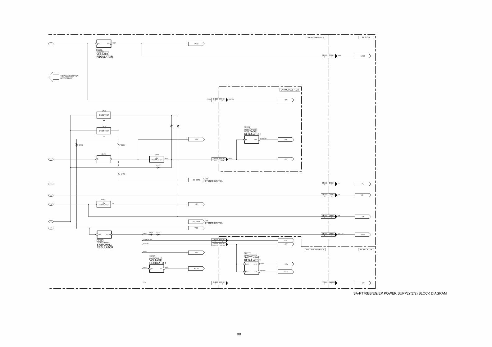
88
1
2
SA-PT70EB/EG/EP POWER SUPPLY(2/2) BLOCK DIAGRAM
TO POWER SUPPLY
SECTION (1/2)
3 IN
VOLTAGEREGULATOR
C0CBABC00117
IP100
IC202
VREF
12V
FL+
FL-
-VP
+3.3V
+3.3V
+1.2V
+6V
VREF
2427
FP8101CN201 NSW+6V
+9V
+5V
FP8101CN201 M+9V
SYS6V
126
CN901CN203
144
CN4001FP8301
SW+3.3V
M+9V
1215
CN901CN203
1316
CN901CN203
FL+
-VP
FL-
117
CN901CN203
OUT 1
5 IN
VOLTAGEREGULATOR
C0CBCDC00063
IC3952
DVD D+5VOUT 4
1 VCC
3 VCC
SWITCHINGREGULATOR
C0DBFZG00001
IC8111
D3.3VD3.3V 6
NSW1.2V1.2V 7
+5V
+5V
+5V
1 2
VREF117
CN901CN203 VREF
Q107
+9V
Q106
DC DETECT
Q105
DC DETECT
FL P.C.B
SCART P.C.B
DVD MODULE P.C.B
DVD MODULE P.C.B
MAIN/D-AMP P.C.B
D204D113
3
4
5
6
7 VDD
DC DET1
-5V
DC DET2
20,2229,31
843
FP8101CN201
12,14,16,1833,35,37,39
FP8101CN201
1041
FP8101CN201
+3.3V3 IN
VOLTAGEREGULATOR
C0CBABC00117
IC107
D3.3VOUT 1
+5V
1 VIN
SWITCHINGREGULATOR
C0DBAYH00005
IC106
SW5V
DVD D5V
V+5V
DVD ADAC+5V
SW5V
SW5V
VOUT 2
D703 D702
D402
D110
TO
SYSTEM CONTROL
TO
SYSTEM CONTROL
REGULATOR
-5V
Q2011
-5VREGULATOR
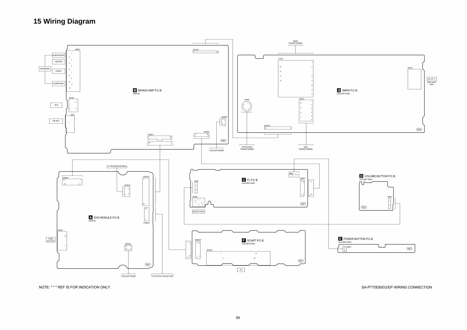
89
15 Wiring Diagram
SA-PT70EB/EG/EP WIRING CONNECTION
B MAIN/D-AMP P.C.B. (SIDE:B)
G SMPS P.C.B. (SOLDER SIDE)
C FL P.C.B.(SOLDER SIDE)
F SCART P.C.B.(SOLDER SIDE)
E POWER BUTTON P.C.B.(SOLDER SIDE)
D VOLUME BUTTON P.C.B.(SOLDER SIDE)
JK401
JK100
CN201
CN203
CN206
CN103
JK51
SUBWOOFER
CENTER
FRONT
SURROUND
AUX
FM ANT
SPEAKERS
3
2
1
1
12
11
10
9
8
7
6
5
4
3
2
501
50 1
2
1
16
17
21
78
151
1
AV
H902
CN901
13
21
1617
21
1617
H903
1
3
21
20
H901*1
3
H2016*
T2900
T5701
T5751
SWITCHING
TRANSFORMERFOR SOFTWARE
SUB
TRANSFORMER
MAIN
TRANSFORMER
15 1
9
8
76 5
4
3
21
15
14
13
12
8
6
4
2
1
5
7
10
7
8
9
6
1
2
3
4
5
P5701
220V-240V
50Hz
AC IN
PbF
PbF
PbF
PbF
PbF
PbF
NOTE: " * " REF IS FOR INDICATION ONLY.
FP8031
FP8251
TO OPTICAL PICKUP UNIT
TO TRAVERSE/SPINDLE
FP8101
FP8531
P3901
FP8301
HDMI
(AV OUT)
1
10 2
9
1
7
2
6
1
50
1
24
19
1
117
216
A DVD MODULE P.C.B. (SIDE:B)
MUSIC PORT
JK902
H904
7
6
5
4
3
2
1
1
3
JK4001
CN4001
2
1
12
1716
12
1716
PbF
FOR SOFTWARE

90
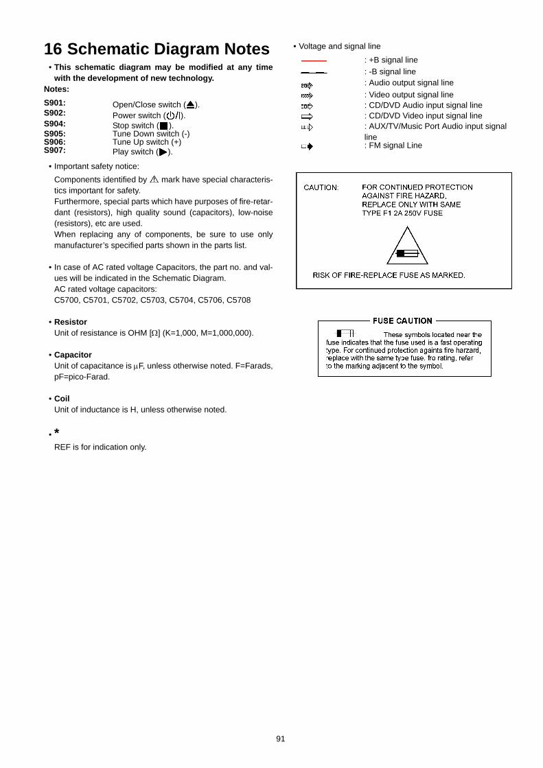
16 Schematic Diagram Notes• This schematic diagram may be modified at any time
with the development of new technology.Notes:
• Important safety notice:
Components identified by mark have special characteris-tics important for safety.Furthermore, special parts which have purposes of fire-retar-dant (resistors), high quality sound (capacitors), low-noise(resistors), etc are used.When replacing any of components, be sure to use onlymanufacturer’s specified parts shown in the parts list.
• In case of AC rated voltage Capacitors, the part no. and val-ues will be indicated in the Schematic Diagram.AC rated voltage capacitors:C5700, C5701, C5702, C5703, C5704, C5706, C5708
• ResistorUnit of resistance is OHM [Ω] (K=1,000, M=1,000,000).
• CapacitorUnit of capacitance is µF, unless otherwise noted. F=Farads,pF=pico-Farad.
• CoilUnit of inductance is H, unless otherwise noted.
• *REF is for indication only.
• Voltage and signal line
S901: Open/Close switch ( ).S902: Power switch ( ).S904: Stop switch ( ).S905: Tune Down switch (-)S906: Tune Up switch (+)S907: Play switch ( ).
: +B signal line: -B signal line: Audio output signal line
: Video output signal line: CD/DVD Audio input signal line : CD/DVD Video input signal line: AUX/TV/Music Port Audio input signal line: FM signal Line
91

92
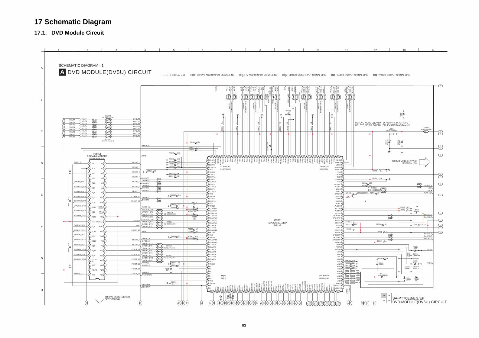
93
17 Schematic Diagram17.1. DVD Module Circuit
AA DVD MODULE(DV5U) CIRCUIT
SCHEMATIC DIAGRAM - 1
SA-PT70EB/EG/EP DVD MODULE(DV5U) CIRCUIT
2/4
4/4
1/4
3/4
P1
10
14
17
18
19
20
2
3
4
5
6
7
8
9
TO DVD MODULE(DV5U)SECTION (2/4)
BE
AQ
AR
AS
AT
AU
AV
AW
AX
AY
AZ
BA
BC
BD
BF
BG
BH BI
BJ
BK
BL
BM
BN
BO
BP
BQ
BR
BS
BT
BU
BV
BW
BX
BY
BZ
CA
CB
CC
CD
CE
CF
CG
CH
CI
CM
CJ
CK
CL
: +B SIGNAL LINE : TV AUDIO INPUT SIGNAL LINE : CD/DVD VIDEO INPUT SIGNAL LINE : VIDEO OUTPUT SIGNAL LINE: CD/DVD AUDIO INPUT SIGNAL LINE : AUDIO OUTPUT SIGNAL LINE
A
B
C
1 2 3 4 5 6 7 8 9 10 11 12 13 14
FODRV
TRDRV
R8225
C8222820P
C82261000P
R82218.2K
8.2K
C8301 6.3V220
C83026.3V33
1000PC8221
1000P
C8225
J0JHC0000045LB8001
LB8011J0JHC0000045
1200PC8211 R8211
10K
8
6 5
7
1
3
2
4
8
6 5
7
1
3
2
4
DVOUT7
DVOUT2
DVOUT4
DVOUT3
DVOUT0
DVOUT1
DVOUT6
D1H84714A043RX3707
D1H84714A043RX3708
DVOUT5
R9084
R9047 10K
4747R9083
VOUT6
VOUT4
VOUT2
VOUT0
VOUT1
VOUT3
VOUT5
VOUT7VOUT6
VOUT4
VOUT2
VOUT0
VOUT1
VOUT3
VOUT5
VOUT7
IC8651
VH
ALF
MD
Q_5
DQ
M1
RX
8019
D1H
422020001
DQ
M0
NC
AS
NR
AS
NC
SM
RX
8018
D1H
422020001
22R8011
NW
ER
8012
22
C8003
0.1
C8013
0.1
MD
Q_6
MD
Q_9
C8014
0.1
MD
Q_7
RX
8014
D1H
88204A
043
MD
Q_8
MD
Q_12
MD
Q_1
MD
Q_0
MD
Q_14
MD
Q_2
MD
Q_13
MD
Q_11
MD
Q_10
MD
Q_4
D1H
88204A
043
RX
8013
MD
Q_3
D1H
88204A
043
RX
8012
C8015
0.1
MA
_4
MA
_3
10KR9045
EXADR_0
C8004
0.1
R9042
10K
C8016
0.1
C8012
0.1
207 173174 166 165167 163164171 170172 168169187188 184 183186 185191 189190 178 177181182 179180194 193203204 200202 201206 205 196 195199 197198 192 175176
106989694929088868482807876747270686664 65 67 69 71 73 75 77 79 81 83 85 87 89 91 93 95 97 99 103100 102101 105104 108107
109
115
113
114
118
117
121
120
125
124
129
130
127
128
135
133
134
139
140
137
136
138
131
132
126
122
123
119
116
110
112
111
161
159
151
152
149
150
154
156
158
157
155
153
141
143
142
147
148
144
146
145
160
162
DV5.0 LSI
MN2DS0018DPIC8001
MA
_6
MA
_0
MA
_1
BA
1
22
R8013
BA
0
D1H
422020001
RX
8020
D1H
88204A
043
RX
8016
D1H
88204A
043
RX
8015
MA
_9
MA
_10
MA
_8
MA
_11
MA
_7
MA
_5
D1H
88204A
043
RX
8017
MA
_2
MA2J1110GLD8211
ADAC-CLK
C8305 0.1
C8304 0.1
4
21
3
RX8401
D1H410120001
J0JCC0000308LB8401
LRCK
SRCK
R8541 15K
R8501 10K
R8502 10K
R8503 10K
R8504 10K
C8202 0.1
4700PC8541
R8314 15K
C8303 0.1
0.1C8005
C8026 0.1
C8001
4V
330
6.3
V100
C8312
1
1
C8313
15KR8313
R8401 100
R8403 100
VIN4
VR
EF
H
VIN3
VIN9
VIN10
1
2
3
4
5
6
7
8
1
2
3
4
5
6
7
8
1
2
3
4
5
6
7
8
1
2
3
4
1
2
3
4
1
2
3
4
1
2
3
4
5
6
7
8
1
2
3
4
5
6
7
8
1
2
3
4
5
6
7
8
1
2
3
4
5
6
7
8
D1H
88204A
043
RX
8011
C8429 0.1
MD
Q_15
VIN1
VIN2
DMIXOUT
MA
9
BA
1
MA
6
MA
0
MA
5
VS
S
HD
HD
HD
HD
HD
HD
HD
HD
MA
2
MA
1
MA
8
MA
7
VS
S
MA
10
MD
Q4
MD
Q3
NW
E
MC
K
BA
0
CLK
CK
E
VS
S
VS
S
VS
S
MD
Q9
MD
Q7
DQ
M1
NC
AS
NC
SM
DQ
M3
DQ
M2
NR
AS
MC
KI
DQ
M0
MD
Q6
MD
Q8
MD
Q5
VD
D33
VD
D33
VD
D33
MD
Q10
VD
D33
VD
D12
VD
D33
MD
Q12
MD
Q11
MDQ0
MDQ1
VS
S
MDQ14
VDD33
OSCO
OSCI
AN
AM
ON
I1
VIN
4R
F
VR
EF
H5
LP
C2
VREFH
LP
CO
2
LP
C1
LP
CO
1
VHALF
VR
EF
L5
VIN
3R
F
RF
INP
RF
INN
VIN
2R
F
VIN
1R
F
[107]AVDDB
VIN4
VIN3
VIN2
VIN6
VIN8
VIN7
AD4
PWM1
VREF
SRCK
LRCK
ROUT
LOUT
PWM0
AD0
VIN1
AD2
AD1
AVDDH
COMP2
AVSSI
ADOUT
AVDDI
AVSSF
AVDDE
AVSSG
DACCK
AVDDG
AVSSE
COMP1
AVDDF
IREF1
DAC4OUT
DAC5OUTDAC4OUT
DAC5OUT
DAC3OUT
DAC1OUT
DAC2OUTDAC3OUT
DAC1OUT
DAC2OUT
AVSSH
[108]AVSSB
VIN10
VIN5
VIN9
AN
AM
ON
I2
EX
TR
G0
VD
D12
AV
SS
D
CC
AP
A
AV
DD
C
CD
AT
A
AV
SS
C
AV
DD
D
VS
S
TR
CS
T
PLF
IL1
VR
EF
L7
VR
EF
H7
EX
TR
G1
TR
CC
LK
TR
CD
AT
A3
TR
CD
AT
A2
TR
CD
AT
A1
TR
CD
AT
A0
DR
V1
DR
V2
VS
S
FG
NR
ST
DR
V0
SC
LO
CK
SD
AT
A
VD
D33
DR
V3
VSS
IECOUT
VDD12[164]MDQ2MDQ15[163]MDQ13
VSS
INN
ER
_S
W
R8406 10
HD: DVD MODULE(HDMI): SCHEMATIC DIAGRAM - 5DV: DVD MODULE(DV5U): SCHEMATIC DIAGRAM 1 - 4
C8011
10K
R9082
TO DVD MODULE(DV5U)SECTION (3/4)
AC
AD
AE
AF
AG
AH AI
AK
AL
AN
AO
AP
AA
P1
AM
D
E
F
G
H
R9044
R9046
R9023
R9048
R9049
EXADR13_DT9
EXADR2_DT7
EXADR1_DT15
EXADR14_DT1 FEXDT_7
EXADR3_DT14
DVOUT1
DVOUT0
0.1C8020
DVOUT2
FEXDT_12
FEXDT_13
EXADR1_DT15
FEXDT_11EXADR2_DT7
FEXDT_14
FEXDT_15
EXADR_17
EXADR_18
EXADR_20
XWE
FEXDT_9
FEXDT_10
FEXDT_8
EXADR4_DT6
EXADR5_DT13
C8652
0.1
EXADR3_DT14
EXADR7_DT12
EXADR9_DT11
EXADR11_DT10
EXADR12_DT2
EXADR10_DT3
EXADR8_DT4
EXADR6_DT5
C8651
0.1
47R9086
R9041 10K
47R9087
C8022
0.1
C8007 0.1
R9088 47
CPU-CMD
CPU-STAT
TRVFTMUTE
SPMUTE
0.1C8021
EXADR_18
EXADR_17
XWE
EXADR_20
10KR9040
R9085 47
R9080
10K
10KR8001
R8003 10K
EXADR_0
D1H85604A043
RX9017
EXADR0_DT0
0.1C8006
EXADR_16
EXADR_16
EXADR9_DT11
EXADR11_DT10
8
65
7
1
3
2
4
8
65
7
1
3
2
4
8
65
7
1
3
2
4
8
65
7
1
3
2
4D1H85604A043
RX9014
EXADR15_DT8
EXADR13_DT9
EXADR12_DT2
EXADR14_DT1
EXADR10_DT3
EXADR8_DT4
R9043 10K
10K
10K
10K
10K
10K
0.1C8018
DVOUT3
EXADR5_DT13
EXADR7_DT12
RX9015
D1H85604A043
EXADR6_DT5
DVOUT5
DVOUT7
RSTB
DVOUT6
EXADR4_DT6
D1H85604A043
RX9016
DVOUT4
FEXDT_3
FEXDT_2
FEXDT_1FEXDT_0
FEXDT_6
FEXDT_5EXADR0_DT0
EXADR15_DT8
FEXDT_4
22
23
21
14
15
13
18
17
20
19
16
3
5
4
6
1
2
12
10
8
7
9
11
26
28
30
32
39
40
36
37
34
35
38
47
45
46
48
41
43
44
42
33
31
29
27
2425
32M FLASH MEMORYRFKWMH42B3D0 215 213 211 209 208210212214
62605856 57 59 61 63
2
4
3
1
8
9
5
7
6
11
10
17
16
19
18
13
15
14
26
27
22
23
20
21
25
24
12
216
53
50
51
46
48
47
42
43
38
39
34
35
30
31
28
29
33
32
37
36
41
40
45
44
49
52
54
55
EXDT2
EXDT1
MA
4
VS
S
MA
3
EXDT9A0 A1 E
XA
DT
0
NE
XO
E
NE
XC
E
VD
D12
A3VSSVDD33
XWE
A20
XRESETXRESET
A9
A12
A13
A10
A11
A15
A14
A8
A19
DQ4
DQ12
VDD
VSS
A16
DQ6
DQ5
DQ7
XBYTE
DQ15/A-1
DQ13
DQ14
A18
A6
A4
A5
A7
A17
NC
WP/ACC
RDY/XBSY
DQ2
DQ10
DQ1
DQ0
XOE
DQ8
DQ9
DQ3
DQ11
EXDT5
VSS
EXDT7
VSS
P3
P1
P2
P5
P7
P6
P4
P0
VSS
VSS
VSS
NEXWE
VDD12
VDD33
VDD33
VDD12
VDD33
EXDT6
EXDT3
EXDT4
VSSXCE A2
EXDT11
EXDT13
EXDT15
EXADT14
P13
P14
DR
V5
DR
V4
EXADT11
EXADT12
EXADT8
EXADT3
EXADT1
EXADT2
EXADT6
EXADT7
EXADT4
EXADT5
EXADT9
P11
P10
P12
[55]P8
[56]P9
EXADR19
EXADR17
EXADR18
EXADT10
EXADT13
EXADR16
EXADT15
EXDT14
EXDT12
[215]STBDACEXDT10
[216]FPGACS
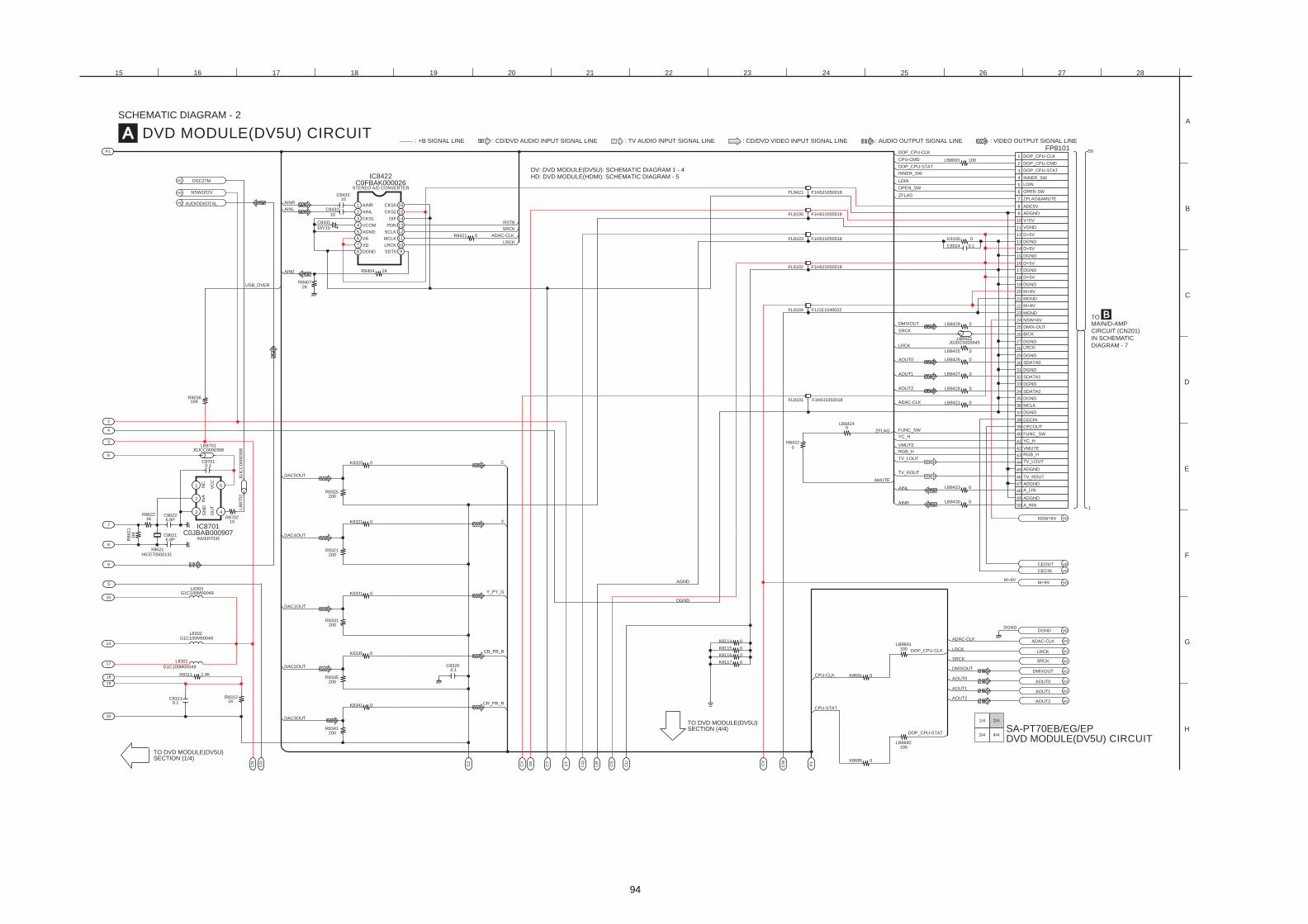
94
TO DVD MODULE(DV5U)SECTION (4/4)
P1
CS
CU
CV
CW
2
P1
A DVD MODULE(DV5U) CIRCUIT
SCHEMATIC DIAGRAM - 2
SA-PT70EB/EG/EP DVD MODULE(DV5U) CIRCUIT
2/4
4/4
1/4
3/4
BTOMAIN/D-AMP
CIRCUIT (CN201)
IN SCHEMATIC
DIAGRAM - 7
: +B SIGNAL LINE : TV AUDIO INPUT SIGNAL LINE : CD/DVD VIDEO INPUT SIGNAL LINE : VIDEO OUTPUT SIGNAL LINE: CD/DVD AUDIO INPUT SIGNAL LINE : AUDIO OUTPUT SIGNAL LINE
15 16 17 18 19 20 21 22 23 24 25 26 27 28
A
B
D
E
F
H
G
C
IC8422C0FBAK000026
98
7
6 11
10LRCK
SDT0
MCLKVA
VD
DGND
5
4
3
2
1 16
15
14
13
12
PDN
R8404AIN0 1K
DIF
CKS0
CKS2
SCLKAGND
AINL
VCOM
CKS1
AINRAINL
AINR
RSTB
AOUT2AOUT2
AUDIODIGITAL
AOUT0AOUT0
AOUT1AOUT1
OSC27M
DGNDDGND
AINL
AINR
100LB8691
100LB8692
0LB8423
0LB8430
M+9VM+9V
STEREO A/D CONVERTER
0R8421
CPU-CLK
CPU-STAT
SRCK
LRCK
SRCK
LRCK
DMIXOUTDMIXOUT
ADAC-CLKADAC-CLK
C8431
C8432
C843310
10
16V10
AOUT1
AOUT2
LRCK
DMIXOUT
AOUT0
AMUTE
USB_OVER
SRCK
ADAC-CLK
ADAC-CLK
DGND
AGND HD
NSW+6V HD
CECIN HD
CEOUT HD
HD
HD
HD
HD
NSW1R2VHD
HD
HD
HD
HD
HD
HD
FL8101 F1H0J1050018
HD: DVD MODULE(HDMI): SCHEMATIC DIAGRAM - 5DV: DVD MODULE(DV5U): SCHEMATIC DIAGRAM 1 - 4
LB8693 100
K8114 0
K8115 0
K8116 0
K8117 0
10KR9036
2KR8407
K8691 0
K8695 0
ZFLAG
INNER_SW
K8100 0
C8024 0.1
F1J1E1040022FL8104
F1H0J1050018FL8102
F1H0J1050018FL8103
F1H0J1050018FL8105
F1H0J1050018FL8421OPEN_SW
ZFLAG
LDIN
6
7
5
9
47
44
39
40
35
31
27
24
21
20
22
16
15
18
17
11
13
12
10
14
19
23
26
25
30
28
29
34
32
33
38
36
37
43
41
42
46
45
49
48
8
1
1
50
3
4
2
50
FP8101
0R8422
LB8422J0JDC0000045
LB8427
LB8426
LB8428
LB8429
LB8421
LB8425 0
0
0
0
0
0
LB84240
DGND
DGND
DGND
MGND
RGB_HRGB_H
VMUTEVMUTE
MGND
BICK
DGND
DGND
DGND
DGND
MCLK
DGND
DGND
LRCKLRCK
SRCK
SDATA1
SDATA2
SDATA0
FUNC_SWFUNC_SW
M+9V
YC_HYC_H
CECIN
CECOUT
A_LIN
ADGND
A_RIN
ADGND
ADGND
TV_ROUTTV_ROUT
TV_LOUTTV_LOUT
M+9V
D+5V
D+5V
D+5V
V+5V
VGND
ADC5V
ADGND
D+5V
DGND
LDIN
INNER_SW
OPEN SW
NSW+6V
DMIX-OUT
ZFLAG&AMUTE
DOP_CPU-CLK
DOP_CPU-CMD
DOP_CPU-STAT
DOP_CPU-CLK
CPU-CMD
DOP_CPU-STAT
DOP_CPU-CLK
DOP_CPU-STAT
TO DVD MODULE(DV5U)SECTION (1/4)
CN
CO
CQ
CR
CT
CX
DA
CZ
CY
14
17
18
19
20
10
3
6
7
8
9
4
5
3
1
2
4
5
C0JBAB000907IC8701
INVERTER
R83121K
R8311 2.4K
L8302G1C100M00049
L8301
G1C100M00049
C83110.1
C86216.8P
10
G1C100M00049L8303
H0J270500131X8621
C86226.8P
R8621
1M
R8622R87021K
LB
8702
J0JC
C0000308
C87010.1
LB8701J0JCC0000308
R8325200
R8321200
R8331200
R8335200
R8341200
C
Y
Y_PY_G
CB_PB_B
CR_PR_R
INA
VC
C
NC
DAC4OUT
DAC5OUT
DAC3OUT
DAC1OUT
DAC2OUT
OU
T
GN
D
K8325 0
K8321 0
K8331 0
K8335 0
K8341 0
0.1C8320
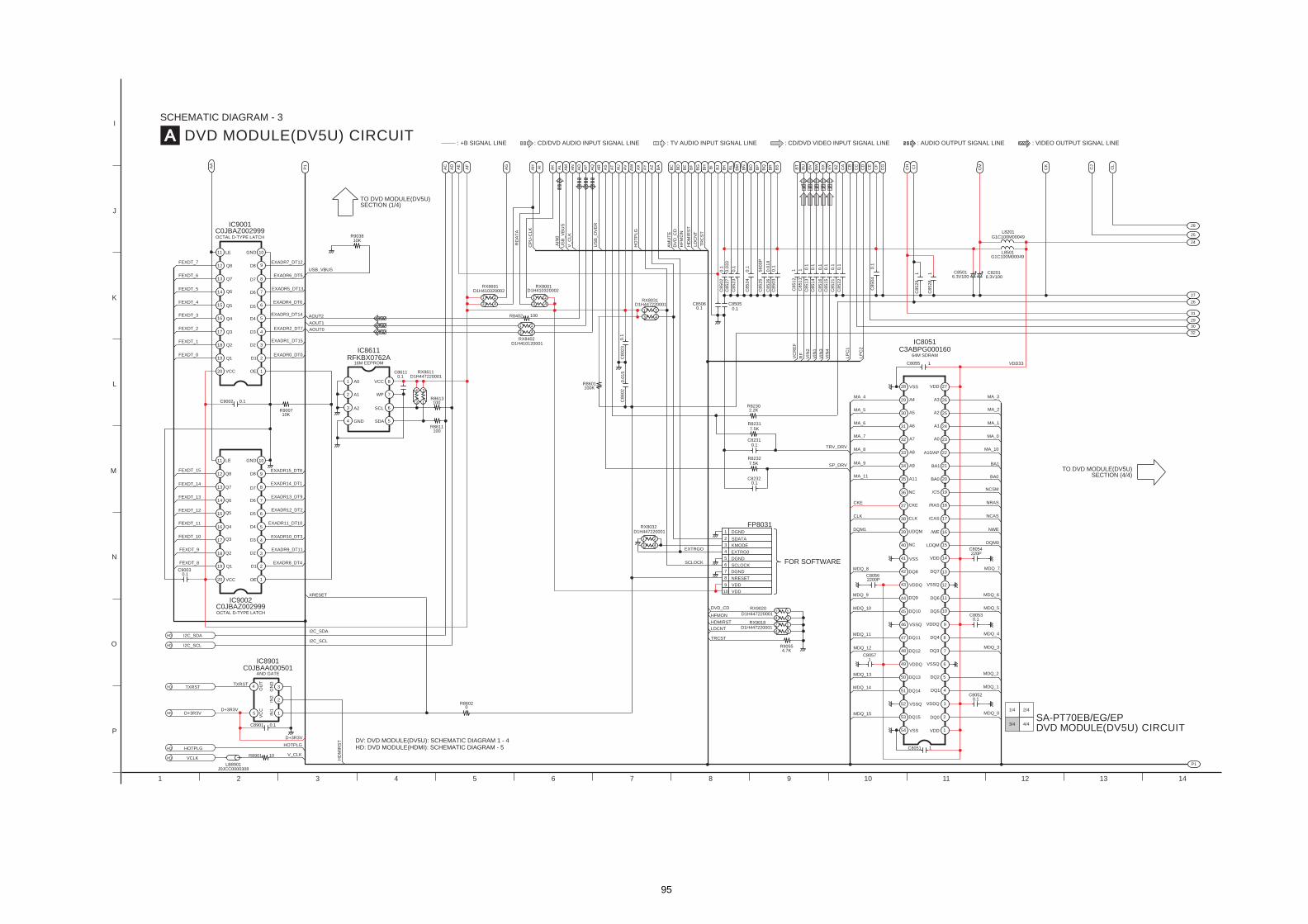
95
A DVD MODULE(DV5U) CIRCUIT
SCHEMATIC DIAGRAM - 3
BEAA
P1
AC
AD
AE
AF
AG
BT
BU
BV
BW
BX
BY
BZ
CA
CB
CC
CD
CE
CF
CG
CH
CI
CM
CJ
CK
CL
AH AI
AK
AL
AN
AO
AP
AQ
AR
AS
AT
AU
AV
AW
AX
AY
AZ
BA
BC
BD
BF
BG
BH BI
BJ
BK
BL
BM
BN
BO
BP
BQ
BR
BS
AM
TO DVD MODULE(DV5U)SECTION (1/4)
TO DVD MODULE(DV5U)SECTION (4/4)
24
25
26
27
28
31
P1
29
30
SA-PT70EB/EG/EP DVD MODULE(DV5U) CIRCUIT
2/4
4/4
1/4
3/4
32
FOR SOFTWARE
: +B SIGNAL LINE : TV AUDIO INPUT SIGNAL LINE : CD/DVD VIDEO INPUT SIGNAL LINE : VIDEO OUTPUT SIGNAL LINE: CD/DVD AUDIO INPUT SIGNAL LINE : AUDIO OUTPUT SIGNAL LINE
8 9 10 11 12 13 14
I
J
L
K
AOUT2
USB_VBUS
FEXDT_6 EXADR6_DT5
FEXDT_4 EXADR4_DT6
EXADR3_DT14FEXDT_3
FEXDT_1 EXADR1_DT15
EXADR0_DT0FEXDT_0
0.0
15
C8602
FEXDT_2 EXADR2_DT7
C8511
1
C8512
1
VIN
4
VIN
3
FEXDT_5 EXADR5_DT13
AOUT1
C8023
0.1
0.1C8505
R8601100K
AOUT0
C85060.1
R8402 100 4
21
3
RX8031D1H447220001
4
21
3
4
21
34
21
3
RX8402D1H410120001
VIN
1
VIN
2
AM
UT
E
LD
CN
T
DV
D_C
D
HO
TP
LG
HD
MIR
ST
TR
CS
T
AIN
0
V_C
LK
US
B_O
VE
R
MDQ_10
DQM1
MDQ_8
MDQ_9
2200PC8056
MDQ_6
MDQ_5
220PC8054
NWE
NRAS
NCAS
MDQ_7
DQM0
MDQ_13
MDQ_15
MDQ_14
MDQ_12
MDQ_11
1C8057
0.1C8052
MDQ_3
MDQ_0
MDQ_2
MDQ_1
0.1C8053
MDQ_4
MA_3
MA_0
MA_1
MA_10
BA0
NCSM
BA1
MA_2
1C8055
MA_6
MA_5
MA_9
MA_11
MA_7
MA_8
MA_4
RX8001D1H410320002
RX8691D1H410320002
EXADR7_DT12FEXDT_7
RD
AT
A
CP
U-C
LK
C8503
0.1
0.0
18
C8513
0.1
C8523
0.1
C8524
0.1
C8502
0.1
0.0
33
C8527
C8525
5600P
C8515
0.1
C8516
C8526
0.1
C8514
0.1
C8504
0.1
C8522
0.1
C8521
0.1
L8501G1C100M00049
G1C100M00049L8201
6.3V100C8501 C8201
6.3V100
C8051 1
C8528
1
C8529
1
29
28
30
31
27
26
24
25
20
21
19
16
12
14
15
13
18
17
9
10
8
7
6
11
2
3
1
4
5
34
36
39
41
42
40
38
49
52
51
54
53
50
44
43
45
47
48
46
37
35
23
22
32
33
64M SDRAMC3ABPG000160
IC8051
SP_DRV7.5KR8232
C82320.1
4
21
3
RX8032D1H447220001
TRCST
R90554.7K
1
2
3
4
8
7
6
5
TRV_DRV
C86110.1
DVD_CD
HFMON
HDMIRST
LDCNT
2.2KR8230
4
2 1
3
4
2 1
3
RX9020
D1H447220001
D1H447220001RX9018
C9002 0.1
R900710K
100R8613
4 2
13
RX8611D1H447220001
7
8
9
6
1
2
5
3
4
12
14
16
18
19
20
17
15
13
1011
C0JBAZ002999IC9001
16M EEPROM
IC8611RFKBX0762A
C82310.1
7.5KR8231
RF
VC
RE
F
LP
C1
LP
C2
A11 BA0
A9 BA1
A1A6
A2A5
VSS VDD
A3A4
A8 A10/AP
A7 A0
DQ11 DQ4
VDDQ
DQ12
VSSQ
DQ3
DQ8 DQ7
NC LDQM
/CS
/CAS
/RAS
NC
CLKCLK
CKECKE
/WEUDQM
VDDVSS
DQ9 DQ6
DQ5DQ10
VSSQ VDDQ
VSSQVDDQ
VDD33
DQ15
VSS
DQ14
VSSQ
DQ0
VDD
DQ1
VDDQ
DQ13 DQ2
OE
D6
D5
D8
D7
D1
D2
D4
D3
GND
Q3
Q2
Q4
Q1
Q7
Q6
Q8
Q5
LE
VCC
OCTAL D-TYPE LATCH
SCL
WP
VCC
SDA
A2
A0
A1
GND
HF
MO
N
6
8
9
7
2
1
4
5
3
10
FP8031
DGND
VDD
VDD
SCLOCK
NRESET
DGND
KMODE
SDATA
EXTRG0EXTRGO
SCLOCK
DGND
US
B_V
BU
S
R903810K
1 2 3 4 5 6 7
M
N
P
O
EXADR14_DT1
EXADR12_DT2
EXADR13_DT9
FEXDT_14
FEXDT_12
FEXDT_13
EXADR15_DT8FEXDT_15
100R8611
EXADR8_DT4
J0JCC0000308LB8901
D+3R3V
D+3R3V
D+3R3V
VCLK
HOTPLG
C8901 0.1
TXRST
IN1
IN2
GN
D
OU
TV
CC
AND GATE
3
1
2
4
5
IC8901C0JBAA000501
TXRST
I2C_SDA
I2C_SCL
V_CLK
HOTPLG
HD
MIR
ST
FEXDT_8
0.1C9003
FEXDT_11 EXADR11_DT10
FEXDT_9
EXADR10_DT3FEXDT_10
EXADR9_DT11
1011
912
813
714
615
516
417
318
219
120
I2C_SDA
R8901
I2C_SCL
XRESET
D3
D4
OE
D2
D8
D6
D5
D7
D1
GND
Q6
Q7
Q3
Q4
Q2
HD
HD
HD
HD
HD
HD
Q5
LE
Q8
Q1
VCC
C0JBAZ002999IC9002
HD: DVD MODULE(HDMI): SCHEMATIC DIAGRAM - 5DV: DVD MODULE(DV5U): SCHEMATIC DIAGRAM 1 - 4
OCTAL D-TYPE LATCH
10
R86020
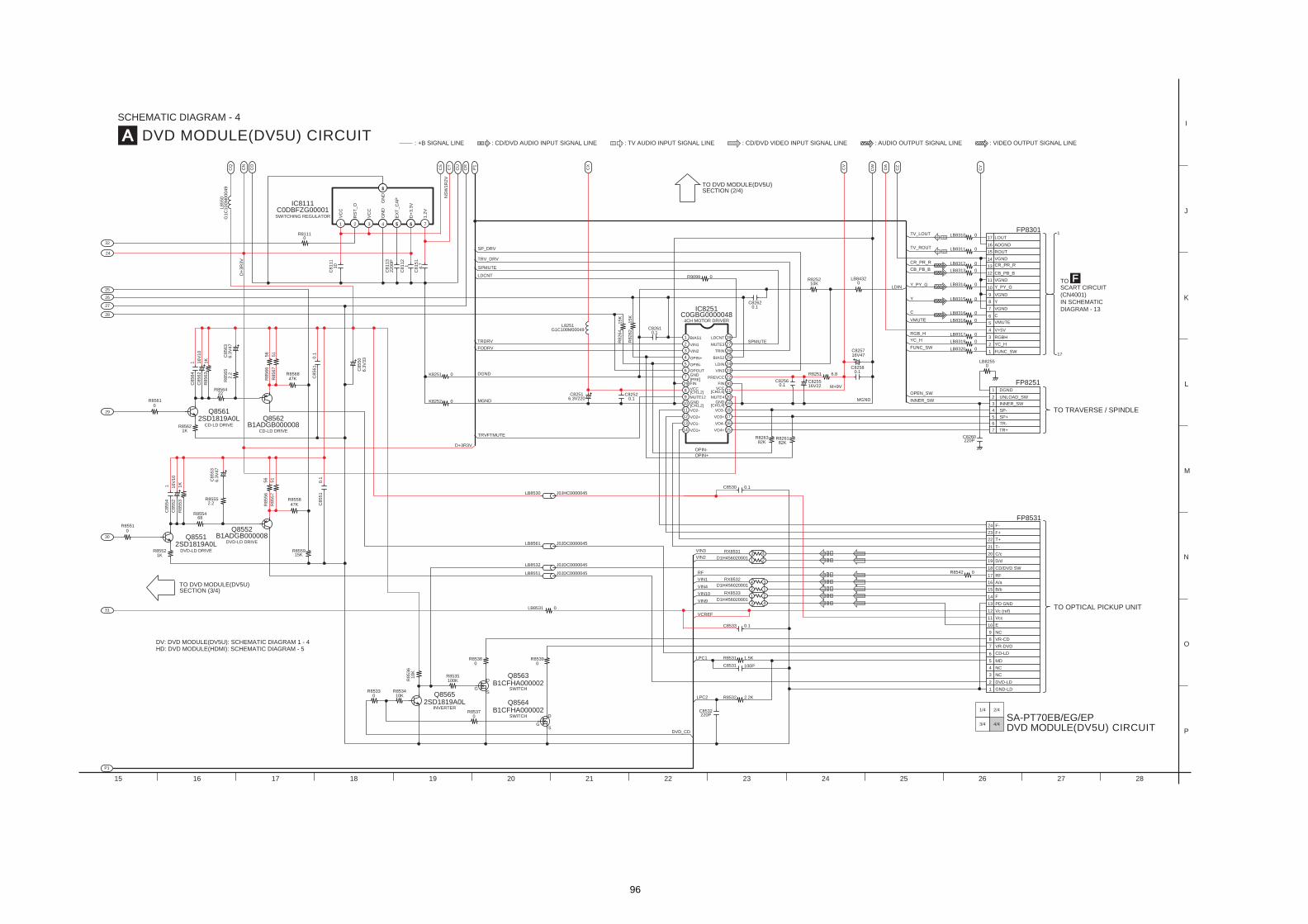
96
25
26
27
28
29
24
32
A DVD MODULE(DV5U) CIRCUIT
SCHEMATIC DIAGRAM - 4
TO DVD MODULE(DV5U)SECTION (2/4)
TO TRAVERSE / SPINDLE
TO OPTICAL PICKUP UNIT
CN
CO
P1
CQ
CR
CS
CT
CU
CV
DA
CX
CW
CZ
CY
SA-PT70EB/EG/EP DVD MODULE(DV5U) CIRCUIT
2/4
4/4
1/4
3/4
FTOSCART CIRCUIT
(CN4001)
IN SCHEMATIC
DIAGRAM - 13
: +B SIGNAL LINE : TV AUDIO INPUT SIGNAL LINE : CD/DVD VIDEO INPUT SIGNAL LINE : VIDEO OUTPUT SIGNAL LINE: CD/DVD AUDIO INPUT SIGNAL LINE : AUDIO OUTPUT SIGNAL LINE
22 23 24 25 26 27 28
I
J
L
M
N
P
O
K
1
1 1
22R8564
47KR8568
0.1
C8561
10
C8111
1C
8112
4.7
C8151
2200P
C8113
R8563
1K
R8567
51
R8566
56
2.2
R8565
C8563
6.3
V47
R826182K82K
R8263
C82580.1
16V47C8257
R8251 6.8
R825210K
LB84320
C825516V22
C82560.1
0.1C8262
3
5
4
2
7
6
FP8251
K8251
R9099
0
K8252 0
0
R8262
15K
R8264
15K
0.1C8261
TRDRV
FODRV
LDCNT
NS
W1R
2V
C82516.3V220 0.1
C8252
1
2
3
4
5
6
7
8
9
29 30
10
11
14
12
13
19
20
21
22
23
24
25
26
27
28
18
15
17
16
4CH MOTOR DRIVERC0GBG0000048
IC8251
SPMUTE
SPMUTE
TRV_DRV
SP_DRV
D+
3R
3V
L8550
G1C
100M
00049
6.3
V33
C8550
C8532220P
C8530 0.1
C8533 0.1
C8531 100P
1.5KR8531
2.2KR8532
4
21
3D1H456020001
RX8531VIN3
VIN2
DVD_CD
Q8562
L8251G1C100M00049
C8562
16V
10
C8564
1
2SD1819A0LQ8561
0R8561
LPC1
LPC2
MUTE4
FIN
LDIN
VIN3
VCC[CH3,4]
M+9V
VO4-
VO4+
VO3+
VO3-
GND[CH3,4]
PREVCC
LDCNT
TRIN
MUTE3
BIAS2
INNER_SW
UNLOAD_SW
1 DGND
SP-
TR-
SP+
MGND
TR+
OPIN-
OPIN+
VO2-
VO1+
VO2+
VO1-
FIN
OPOUT
GND[CH1,2]
MUTE12
VCC[CH1,2]
BIAS1
VIN2
VIN1
OPIN-
OPIN+
GND[PRE]
MGND
DGND
1 2 3 4
VC
C
RS
T_O
VC
C
GN
D
EX
T_C
AP
IC8111C0DBFZG00001
D+
3.3
V
1.2
V
GN
D
0LB8255
SWITCHING REGULATOR
INNER_SW
8
5 6 7
R81110
220PC8260
OPEN_SW
LDIN
17
1
Y_PY_G
CR_PR_R
CB_PB_B
LB8319
LB8318
LB8317
LB8320
Y
C LB8316
LB8312
LB8313
6
5
8
9
11
12
10
14
15
13
7
2
1
4
3
17
16
FP8301
LB8311
LB8315
LB8314
0
0
0
0
0
0
0
0
LB8310 0
0
0
VIN9
VIN10
VIN4
0R8542
4
21
3
RX8533
D1H456020001
4
2 1
3RX8532
D1H456020001
VIN1
6
7
5
9
13
15
14
11
10
12
21
22
18
16
17
20
19
8
1
3
4
2
24
23
FP8531
MD
NC
NC
CD-LD
NC
VR-CD
DVD-LD
GND-LD
VR-DVD
RGB_H
VMUTE
TV_ROUT
TV_LOUT
YC_HYC_H
ROUT
VGND
ADGND
Y
C
VGND
RGBH
VGND
VGND
V+5V
CB_PB_B
CR_PR_R
VMUTE
Y_PY_G
FUNC_SWFUNC_SW
LOUT
E
F
T-
D/d
RF
C/c
F+
T+
B/b
Vcc
A/a
PD GND
CD/DVD SW
Vc (ref)VCREF
RF
F-
TO DVD MODULE(DV5U)SECTION (3/4)
P1
30
31
15 16 17 18 19 20 21
0R8538
0R8539
10K
R8536
100KR8535
0R8537
10KR8534
0R8533
TRVFTMUTE
68R8554
R8553
1K
0LB8531
LB8530 J0JHC0000045
LB8561 J0JDC0000045
LB8532 J0JDC0000045
LB8551 J0JDC0000045
B1CFHA000002Q8563
B1CFHA000002Q85642SD1819A0L
Q8565
47KR8558
15KR8559
0.1
C8551
2.2R8555
6.3
V47
C8553
DVD-LD DRIVE
Q8552B1ADGB000008
CD-LD DRIVE
B1ADGB000008
R8557
51
56
R8556
D+3R3V
R85621K
R85521K
C8554
1
C8552
16V
10
0R8551
DVD-LD DRIVE
2SD1819A0LQ8551
CD-LD DRIVE
S
D
SWITCH
SWITCH
INVERTER
G
S
D
G
HD: DVD MODULE(HDMI): SCHEMATIC DIAGRAM - 5DV: DVD MODULE(DV5U): SCHEMATIC DIAGRAM 1 - 4
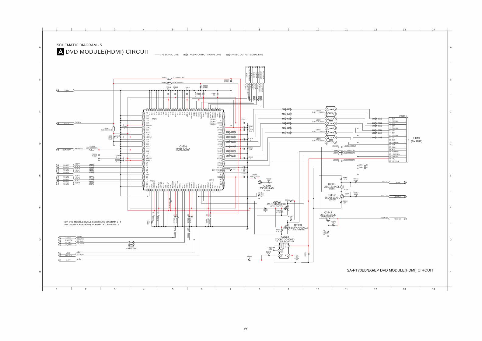
97
: +B SIGNAL LINE
HDMI
(AV OUT)
A DVD MODULE(HDMI) CIRCUIT
SCHEMATIC DIAGRAM - 5
SA-PT70EB/EG/EP DVD MODULE(HDMI) CIRCUIT
: VIDEO OUTPUT SIGNAL LINE: AUDIO OUTPUT SIGNAL LINE
A
B
C
D
1 2 3 4 5 6 7 8 9 10 11 12 13 14
8 9 10 11 12 13 14
A
B
D
E
F
H
G
C
4
3
1
2
4
3
1
2
1C
3956
J0JCC0000042LB3906
R3943100K
R3942220K
2.7KR3946
J0JCC0000042LB3905
R394127K
R3944220
2SD1819A0LQ3941
10K
R3945
Q39432SD1819A0L
C3941
220P
LB3903 J0JCC0000042
4
3
1
2
4
3
1
2
J0JCC0000042LB3904
6
7
5
9
12
10
11
18
19
16
17
13
15
14
8
1
3
4
2
P3901
D+3R3VD+3R3V
1C3917
C3901
LB3901J0JHC0000045
0.1C3929
C39400.1
C39111
AO
UT
1
AO
UT
2
AD
AC
-CLK
DM
IXO
UT
4V330C3904
SR
CK
LR
CK
AO
UT
0
AU
DIO
DIG
ITA
L
AO
UT
1
AO
UT
2
AD
AC
-CLK
DM
IXO
UT
SR
CK
LR
CK
AO
UT
0
AU
DIO
DIG
ITA
L
C39070.1
DGND
LB3907 J0JHC0000045
C39024V330
1C
3909
LB3902 J0JHC0000045
C39140.1
C39100.1 1
C3924
C3908
0.1
C39231
C39280.1
10
MA2J7280GLD3901
R390210K
R3903
10K
0K3903
0K3905
0.01C3955
10KR3947
1C3915
C3913
C39301
NSW1R2VNSW1R2V
LB3908J0JHC0000045
C39064V330
1
0.1C3926
C3932
63 5052 51 4547 46 4142 38 343637 3540 3944 4349 486062 61 5657 5355 5459 5864
80
81
72
67
65
66
71
69
68
70
76
78
79
77
73
75
74
83
82 15
16
14
31
29
23
26
27
24
25
18
19
17
22
20
21
28
30
32
33
2KR3905
R39072K
S
D
G
C3954
S
D
G
3
1
2
4
5
4.7KR3906
4.7KR3904
RSV
CEC
+5V
CLK-
CLK+
D2-
D2+
D1-
D0-
D0+
D1+
CLKGND
HDMISCL
HOTPLG
CECGND
HDMISDA
D2GND
D0GND
D1GND
DV
NSW+6V DV
CECOUT DV
CECIN
NSW+6V
CECOUT
CECINDV
DV
DV
NC
AM
DA
M
VSS
AM
SD
I0
VS
S
VD
D12
AM
RX
AM
DA
WS
VD
D33
AM
SD
I1
AVSS
AVDD
VD
D33
AM
SD
I3
AVSS
AVDD
AVSS
AVDD
TX2P
TX2M
VDD33
VDD12
TX1P
TX1M
AM
SD
I2
[32]NC
[31]NC
[30]NC
TXOP
TX0M
Q39012SD1819A0L
D9
NC
DS
D0
D35
D32
D29
D27
D25
D23
D24
D26
VS
S
D30
D34
D33
VS
S
VD
D33
D22 VD
D12
D20
D18
VSS
D15
D13
D12
D10
D11
VSS
D14
D16
D17
D19
VDD12
VDD33
D21 [65]NC
VD
D12
AM
DA
CL
D31
D28
DV
DV
DV
DV
DV
DV
DV
DV
OU
TIN
GN
DN
ois
eB
ypass
VC
IC3901MN864702AHDMI TRANSMITTER
LEVEL SHIFTER
LEVEL SHIFTER
VOLTAGE REGULATOR
Q3903B1CFHA000002
IC3952C0CBCDC00063
Q3902B1CFHA000002
BUFFER
L3903G1BYYYC00026
L3904G1BYYYC00026
L3905G1BYYYC00026
L3906G1BYYYC00026
POWER SUPPLY
2SD1819A0LQ3942
DIODE
SWITCH
4V
330
0.1
K3911 0.1
K3909 0.1
E
F
G
H
1 2 3 4 5 6 7
VOUT6
VOUT7
VOUT4
VOUT1
VOUT2
VOUT0
VOUT3
R3901 5VOUT5
VOUT6
VOUT7
VOUT4
VOUT1
VOUT2
VOUT0
VOUT3
VOUT5
00.1
C3916
R3924
C3925
0.1
C3927
1 0.1
C3921
C3918
0.1
0.1
C3964
C3919
1
TXRST
R3921
0
C3920
1
10K
R3925
HOTPLG
VCLK
M+9V
4
2 1
3
RX3901D1H410120001
OSC27M
I2C_SDA
I2C_SCL
TXRST
HOTPLG
VCLK
M+9V
OSC27M
I2C_SDA
I2C_SCL
0.1
0.1C3922
127125123117116 118115 120 1211199897 99 105104 106102100 101 103 113111109108 110 112 114107 122 124 126
95
92
93
88
89
84
85
87
86
91
90
94
96
9
10
7
8
12
13
11
1
4
2
3
6
5
128
DV
DV
DV
DV
DV
DV
DV
DV PVDD1
TXCM
PVSS1
EXT_SWING
AVDD
AVSS
TXCP
NC
NC
PV
DD
2
NC
NC
NC
PV
SS
2
HP
D
VS
S
SC
L
VS
S
VD
D12
SD
A
NC
NC
VDD12
[1]NC
D7
D5
D3
D1
D0
D2
D4
D6
D8
VD
D12
PC
LK
IN
VD
D12
NR
ES
ET
HC
LK
HC
LK
DIV
NC
VSS
NC
VDD12
VDD33
LP
SA
VS
S
HS
YN
C
NIR
Q
NT
ES
T
DE
[96]NC
VD
D12
VD
D33
VS
YN
C
HS
CL
HS
DA
VD
D33
VS
S
DV
DV
DV
DV
DV
DV
DV
HD: DVD MODULE(HDMI): SCHEMATIC DIAGRAM - 5DV: DVD MODULE(DV5U): SCHEMATIC DIAGRAM 1 - 4
C3965
10P
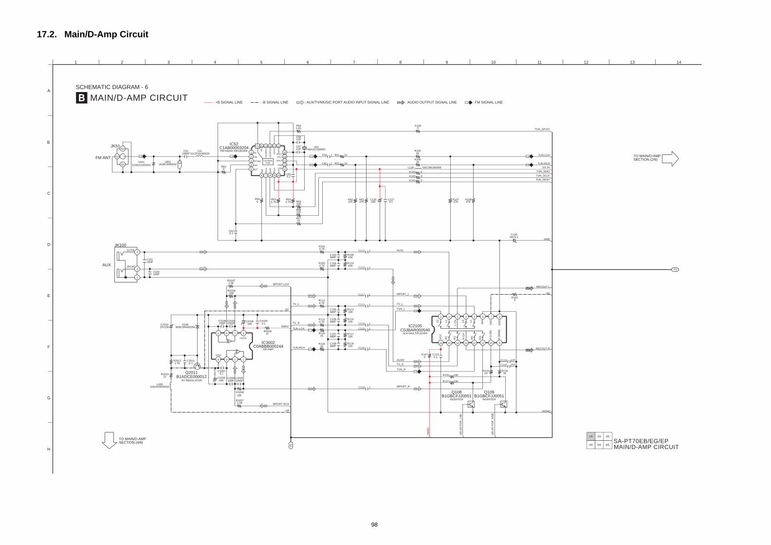
98
17.2. Main/D-Amp Circuit
P1
TO MAIN/D-AMPSECTION (2/6)
SA-PT70EB/EG/EP MAIN/D-AMP CIRCUIT
2/6 3/6
5/6
1/6
4/6 6/6
MAIN/D-AMP CIRCUIT
SCHEMATIC DIAGRAM - 6
B: +B SIGNAL LINE : -B SIGNAL LINE : AUX/TV/MUSIC PORT AUDIO INPUT SIGNAL LINE : AUDIO OUTPUT SIGNAL LINE : FM SIGNAL LINE
A
B
C
D
1 2 3 4 5 6 7 8 9 10 11 12 13 14
GND
SW
5V
K1470
R52 1K
R51 1K
C1230.1
0.1C61
R56220
R55220
R571K
R592.2K
22PC58
22PC57
R630
G2
G3
G1
JK51
FM ANTVA51
EZAEG2A50AX
LB51J0JBC0000032
C511000P
4.7KR101
0.1C62
R534.7K
R544.7K
R640
L51G1CR18JA0020
JK100
4 12
1
2 14
T1 1719 18 16
15
20
3 13THERMALPAD
5 11
108 976
C1AB00003204FM RADIO RECEIVER
IC52
C60 1
C59 1
X51H0A327200097
111 1
112 1
115 1
116 1
117 1
118 1
113 1
114 1
1KR105
1KR106
C126100
C1270.1
0K141
K143 0
0K142
L120 G0C390JA0055
0K140
TUN_GP102
R10747K
R10847K
TUN-RCH
TUN-LCH
D3.3V
TUN_SCLK
TUN_SDIO
TUN_REST
SE
LE
CT
OR
_L
SB
1KR125
1KR130
SE
LE
CT
OR
_M
SB
AGND
B1GBCFJJ0051Q108
B1GBCFJJ0051Q109
0R103
-5V
C119 47P
C120 47P
RECOUT-L
RECOUT-R
10KR126
10KR127
R6247K
R6147K
75 61 432
1012141516 13 11
8
9
C0JBAR0005404CH MULTIPLEXER
IC2105
C13650V3.3
A (
LS
B)
VE
E
INH
R3
B (
MS
B)
GN
DL2
L C
H
R2
R1
VC
C
TV_R
AUXR
AUXL
TUN_R
L0
TV_L
TUN_L
MPORT_L
MPORT_R
RST
SE
NN
C
RFGND
FMI
NC
AMI GND
ROUT
RC
LK
VIO
VDD
SC
LK
SD
IO
DF
S
DC
LK
GC
GP
O2
LOUT
DOUT
GC
GP
O1
[LCH]
L1
R0
L3
R C
H
INVERTER INVERTER
P1
TO MAIN/D-AMPSECTION (4/6)
E
F
G
H
330PC3106
L428G0A200D00002
C201025V100
D106B0BC5R6A0266
R20122.7K
R201022
0.1C3207
100C3208
0.1C2011
330PC3206
SW5V
R3209476 75
24 3
8
1
IC3002C0ABBB000244
OP-AMP
Q2011B1ADCE000012
-5V
R3208
10K
C32051000P
C103680P
C104680P
R10910K
10KR110
C105680P 10K
R113
C106680P 10K
R114
C107680P 10K
R117
C108680P 10K
R118
C101100P
TV_L 4.7KR111
4.7KR112
1KR115
1KR116
4.7KR102
C102100P
1
2
3
TV_R
TUN-LCH
C3108100
C31040.1
MPORT-LCH
C31051000P
10KR3108
1.5KR3107
MPORT-RCH
-VP
1.5KR3207
TUN-RCH
C
C
C
C
C
C
C
C
+VCC
-VCC
[RCH]AUX
-5V REGULATOR
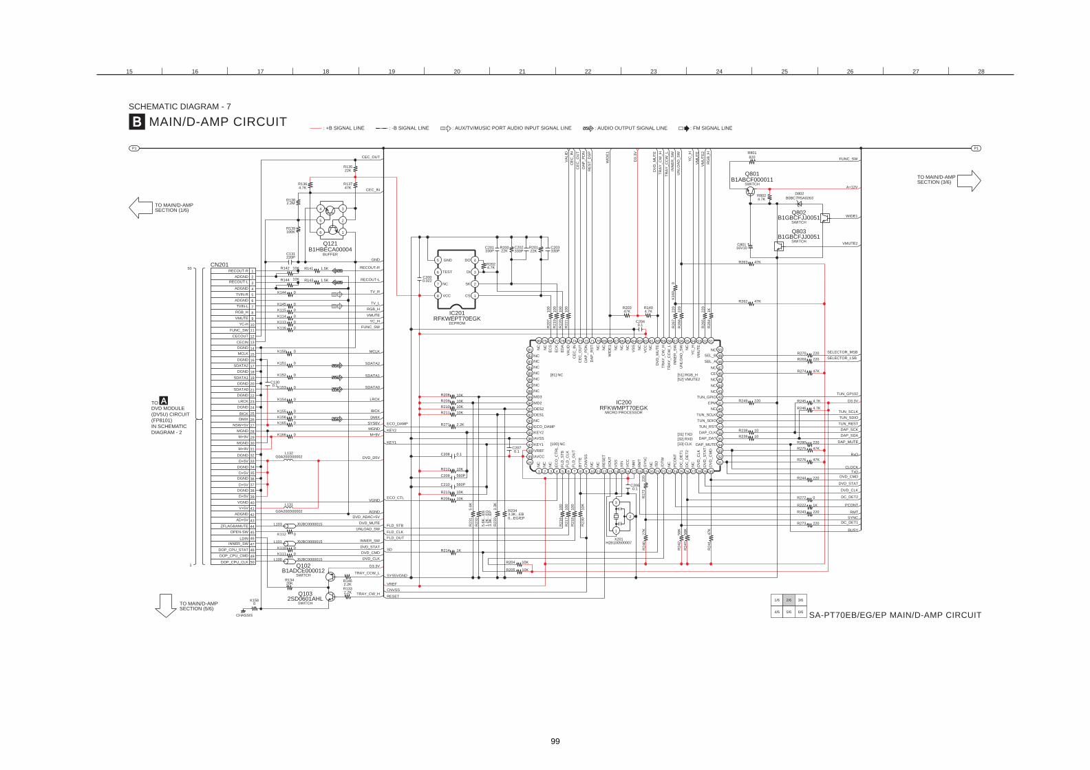
99
P1 P1
TO MAIN/D-AMPSECTION (1/6)
TO MAIN/D-AMPSECTION (3/6)
SA-PT70EB/EG/EP MAIN/D-AMP CIRCUIT
2/6 3/6
5/6
1/6
4/6 6/6
MAIN/D-AMP CIRCUIT
SCHEMATIC DIAGRAM - 7
B
50
: +B SIGNAL LINE : -B SIGNAL LINE : AUX/TV/MUSIC PORT AUDIO INPUT SIGNAL LINE : AUDIO OUTPUT SIGNAL LINE : FM SIGNAL LINE
15 16 17 18 19 20 21 22 23 24 25 26 27 28
WIDE1
VMUTE2
A+12V
GND
Q803B1GBCFJJ0051
B1GBCFJJ0051Q802
D802
B0BC7R5A0263R8024.7K
220R280
R275 47K
DAP_MUTE
DAP_SDA
47KR276
R263 47K
47KR262
TUN_REST
DAP_SCK
4.7KR245
4.7KR246
TUN_SDIO
D3.3V
TUN_SCLK
R1404.7K
R20347K
DV
D_
MU
TE
TR
AY
_C
W_
H
R2024.7K
C2000.022
C203330P
C202330P
R20122K
C201330P
R20022K
10
0R
20
7
CEC_IN4.7KR136
R13522K
CEC_OUT
2.2MR138
47KR137
6
7
5
2
4
3
8 1
RFKWEPT70EGKEEPROM
IC201
0.1C204
WID
E1
VA
LID
10
0R
22
0
10
0R
22
1
D3
.3V
CE
C_
OU
T
CE
C_
IN
RE
ST
_D
SP
DA
P_
PD
N
10
0R
21
9
R270 220
R2
65
22
0
R2
64
1K
R2
66
22
0
R2
67
22
0
Q801B1ABCF000011
SELECTOR_MSB
R269 220 SELECTOR_LSB
INN
ER
_S
WK
16
00
C80116V10
UN
LO
AD
_S
W R801
820 FUNC_SWYC
_H
TR
AY
_C
CW
_L
RG
B_
H
VM
UT
E2
VM
UT
E
0K116
0K113
VMUTE
FUNC_SW
YC_H
0K150 MCLK
R139100K
C131220P
RECOUT-R
0K145
0K144
0K114
0K115
R141 1.5KR142 10K
R144 10K
6
7
5
9
11
13
12
10
14
8
1
3
4
2
CN201
R143 1.5K
TV_L
RGB_H
RECOUT-L
TV_R
2
3
1
5
4
6
B1HBECA00004Q121
DVD_CMD
0.1C206
R243 220
220R244
0R272
1KR222
22
0R
17
2
RMT
DC_DET2
SYNC
PCONT
DVD_STAT
DVD_CLK
47
KR
24
1
27
KR
24
0
56
KR
24
7
DC_DET1220R273
56
KR
24
2
3
1
2
X201H2B100500007
R2
30
10
K
10
0R
21
8
10
0R
21
7
10
0R
21
6
TUN_GP102
R249 220
10R238
R239 10
3 42 5
98
94
95
92
91
93
97
96
1
100
99
80 78 767779
87
86
88
89
82
84
83
81
85
90
1614 15 1711 1312
69 67 65 64666870 51
49
45
47
46
41
44
42
43
48
50
30
39
37
35
32
31
34
33
36
38
40
22 2320 21 26 282724 2518 19
53555762 60 596163 58 56 54
29
5275 73 717274
976 8 10
IC200RFKWMPT70EGK
NC
NC
NC
NC
MD3
VA
LID
ED
A
NC
NC
[81] NC
NC
NC
NC
EC
S
EC
K
TUN_GPIO
TR
AY
_C
W_
H
NC
INN
ER
_S
W
TR
AY
_C
CW
_L
DV
D_
MU
TE
CE
SEL_A
[51] RGB_H
NC
NC
YC
_H
VM
UT
E
SEL_B
NC
UN
LO
AD
_S
W
[52] VMUTE2
NC
NC
NC
CE
C_
OU
T
DA
P_
PD
N
CE
C_
IN NC
VC
C
NC
NC
NC
NC
NC
VS
S
DA
P_
RS
T
WID
E1
FL
D_
CL
K
EC
O_
CT
RL
FL
D_
ST
B
FL
D_
OU
T
MD2
[100] NC
MICRO PROCESSOR
AVCC
NC
NC
NC
VREF
ECO_DAMP
NC
NC
/SD
NM
I
XIN
VC
C
RM
T
SY
NC
TxD
CLOCK
RxD
BUSY
TUN_SDIO
TUN_SCLK
[32] RXD
PC
ON
T
DC
_D
ET
1
[31] TXD
NC
[33] CLK
DV
D_
CM
D
NC
DV
D_
CL
K
DC
_D
ET
2
DAP_DAT
DAP_CLK
TUN_RST
DV
D_
ST
AT
DAP_MUTE
/OT
W
NC
BY
TE
CN
VS
S
VS
S
XO
UT
NC
RE
SE
T
EPM
ADGND
RECOUT-R
SK
DO
DI
CS
NC
TEST
GND
VCC
DES2
RGB_H
YC-H
VMUTE
RECOUT-L
ADGND
ADGND
TVIN-R
TVIN-L
MCLK
DGND
FUNC_SW
CECIN
CECOUT
KEY2
AVSS
KEY1
DES1
NC
BUFFER
SWITCH
SWITCH
SWITCH
47KR274
TO MAIN/D-AMPSECTION (5/6)
1
ATODVD MODULE
(DV5U) CIRCUIT
(FP8101)
IN SCHEMATIC
DIAGRAM - 2
ECO_CTL
RESET
CNVSS
R213 10K
R206 10K
VREF
R212 10K
0K158
K166 0
K165 0
0K110
K111 0
0K112
0K152
0K154
0K155
0K156
0K153
0K151
2.2KR1332.2KR146
0.1C130
B1ADCE000012Q102
J0JBC0000015L103
J0JBC0000015L101
J0JBC0000015L100
L132G0A200D00002
L131
G0A200D00002
R13420K
2SD0601AHLQ103
DVD_D5V
LRCK
SDATA2
SDATA0
SDATA1
DMIX
BICK
SYS6V
DVD_CLK
TRAY_CW_H
TRAY_CCW_L
D3.3V
UNLOAD_SW
DVD_CMD
DVD_STAT
DVD_MUTE
DVD_ADAC+5V
AGND
INNER_SW
R209 10K
R208 10K
R211 10K
R210 10K
ECO_DAMP 2.2KR271
47
44
39
40
35
31
27
24
21
20
22
16
15
18
17
19
23
26
25
30
28
29
34
32
33
38
36
37
43
41
42
46
45
49
48
50
C209 560P
560PC210
C208 0.1
R2
31
5.6
K
R2
32
5.6
K..
.EB
1.2
K..
.EG
3.3
K..
.EP R234
3.3K...EB0...EG/EP
R2
33
3.3
K
SD 1KR214
FLD_STB
R204 10K
R205 10K
FLD_CLK
FLD_OUT
M+9V
C2070.1
KEY2
KEY1
MGND
SYS5VGND
VGND
DGND
D+5V
VGND
V+5V
D+5V
D+5V
DGND
AD+5V
DOP_CPU_CMD
DOP_CPU_STAT
DOP_CPU_CLK
CHASSIS
OPEN-SW
ZFLAG&AMUTE
INNER_SW
LDIN
ADGND
SDATA0
DGND
DGND
SDATA2
SDATA1
DGND
DGND
MGND
DGND
DGND
D+5V
M+9V
M+9V
MGND
DGND
LRCK
DMIX
BICK
NSW+5V
SWITCH
SWITCH
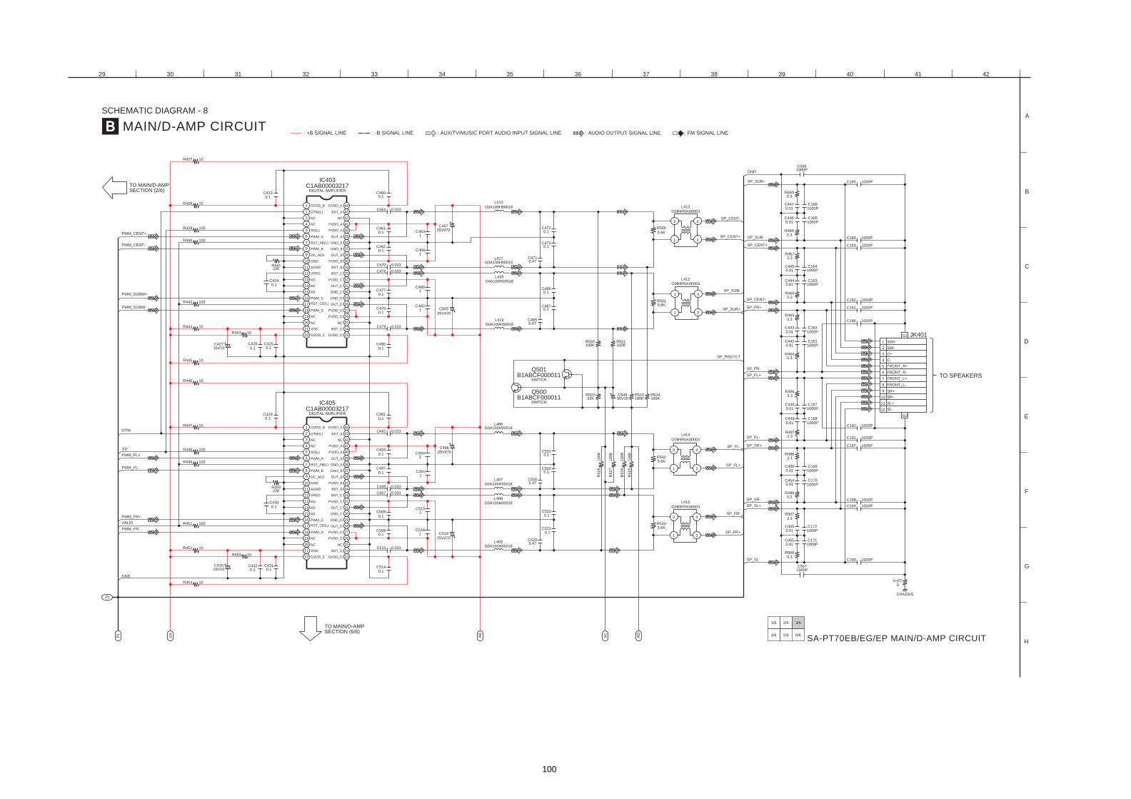
100
AC
AD
TO MAIN/D-AMPSECTION (2/6)
SA-PT70EB/EG/EP MAIN/D-AMP CIRCUIT
2/6 3/6
5/6
1/6
4/6 6/6
B MAIN/D-AMP CIRCUIT
SCHEMATIC DIAGRAM - 8
: +B SIGNAL LINE : -B SIGNAL LINE : AUX/TV/MUSIC PORT AUDIO INPUT SIGNAL LINE : AUDIO OUTPUT SIGNAL LINE : FM SIGNAL LINE
29 30 31 32 33 34 35 36 37 38 39 40 41 42
A
B
D
E
F
H
G
C
SP_SL-
C5671000P
R5063.3
0K157
SP_CENT+
C479 0.033
SP_SUB+
SP_SUB-
PWM_SUBW-
R444 10
C4250.1
SP_CENT-3.3
R466
C185 1000P
R524100K
C184 1000P
BCF000011Q500
BCF000011Q501
R523100K
R521100K
R520100K
33KR522
SP_PROTCT
C1641000P
3.3R467
C4450.01
50V10C548
C1631000P
C4440.01
C4900.1
SP_FL+
3.3R464
3.3R465
C186 1000P
SP_FL-
0.1C501
5.6KR502
C1621000P
1000PC161
C4430.01
2
43
1
G0B9R5K00003
L414
C4420.01
5000.47
0.1C502
SP_FR+
C183 1000P
R5
28
10
0K
C181 1000P
C182 1000P
10
0K
R5
25
R5
27
10
0K
R5
26
10
0K
R443 10
C4260.1
10R445
C42716V10
R428 10
R427 10
C4230.1
C5661000P
0.033C464
SP_CENT-
C4600.1
C4770.1
SP_SUB-
3.3R468
R5015.6K
G0A100H00018L418
C4860.1
C1661000P
C1651000P
C4460.01
C4801
C4780.1
G0A100H00018L419 C485
0.47
C4870.1
2
43
1
L412G0B9R5K00003
C50525V470
C4821
C4240.1
PWM_SUBW+
R442 100
C470 0.033R44122K
R440 100
R429 1005.6KR500
SP_CENT+
L410
G0A100H00018
G0A100H00018L417
SP_SUB+
3.3R469
C4730.1C462
0.11
C466
C4710.47
2
43
1
L413
G0B9R5K00003
C4720.125V470
C467C4610.1
1C463
C476 0.033
43
11
9
10
34
36
35
12 33
6
7
5
39
38
41
40
8 37
2322
20
18
16
14
13
15
17
19
31
32
28
26
25
27
30
29
21 24
3
4
2
1
42
44
IC403
DIGITAL AMPLIFIERC1AB00003217
C4470.01
PWM_CENT-
PWM_CENT+
SP_FL+
SP_FR-
3.3R496
0.1C522
3.3R497
SP_FR+
C192 1000P
SP_FL- C191 1000P
C4490.01
R5035.6K
0.1C523
5200.47
C1671000P
C4480.01
2
43
1
G0B9R5K00003
L415
C1681000P
C4540.01
C190 1000P
1000PC169
0.01C450
SP_SR-
SP_SL+
1000PC170
3.3R499
C187 1000P
3.3R498
C189 1000P
C188 1000P
SP_SR+
SP_FR-
C4550.01 1000P
C171
R5073.3
C1721000P
C4560.01
1
G1
8
9
11
10
12
5
6
2
4
3
7
G2
JK401
GND
CHASSIS
FRONT_R-
C-
FRONT_R+
SR+
SL-
SL+
SR-
FRONT_L+
FRONT_L-
SW-
NC
OUT_C
BST_C
OUT_D
GND_C
GND_D
NC
OUT_A
BST_A
BST_B
GND_A
OUT_B
GND_B
SW+
BST_D
PVDD_D
PVDD_D
PVDD_A
PVDD_B
GVDD_A
PVDD_A
PVDD_C
GVDD_D
C+
NC
M2
NC
NC
M3
M1
GND
NC
VDD
VREG
AGND
PWM_B
PWM_D
PWM_C
SD(L)
PWM_A
OC_ADJ
GVDD_B
OTW(L)
GVDD_C
RST_AB(L)
RST_CD(L)
TO SPEAKERSSWITCH
SWITCH
P1
P1
AA
AB
TO MAIN/D-AMPSECTION (6/6)
OTW
SD
B1A
B1A
C4290.1
C49625V470
C
G0A100H00018L406
C497
0.1
C4930.1
C4911
1C494
C492 0.033
0.1C481
PWM_FL+
PWM_FL-
R448 100
R449 100
R446 10
R447 10
IC405
DIGITAL AMPLIFIERC1AB00003217
PWM_FR+
C508
0.1
G0A100H00018
L408
C5151
C4300.1
0.033C510R452 10
R453 10
PWM_FR-
R451 100
C5161
C5090.1
G0A100H00018L409 C
C51925V470
VALID
C4310.1
C4320.1
10R454
C43316V10
C5140.1
R45022K
C498 0.033
C507 0.033
G0A100H00018L407
GND
43
11
9
10
34
36
35
12 33
6
7
5
39
38
41
40
8 37
2322
20
18
16
14
13
15
17
19
31
32
28
26
25
27
30
29
21 24
3
4
2
1
42
44
NC
OUT_C
BST_C
OUT_D
GND_C
GND_D
NC
OUT_A
BST_A
BST_B
GND_A
OUT_B
GND_B
BST_D
PVDD_D
PVDD_D
PVDD_A
PVDD_B
GVDD_A
PVDD_A
PVDD_C
GVDD_D
NC
M2
NC
NC
M3
M1
GND
NC
VDD
VREG
AGND
PWM_B
PWM_D
PWM_C
SD(L)
PWM_A
OC_ADJ
GVDD_B
OTW(L)
GVDD_C
RST_AB(L)
RST_CD(L)
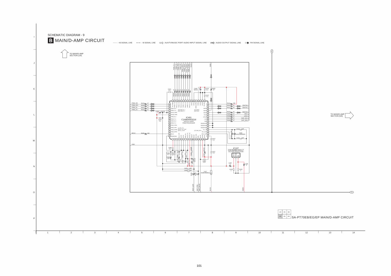
101
P1
P1
TO MAIN/D-AMPSECTION (5/6)
TO MAIN/D-AMPSECTION (1/6)
SA-PT70EB/EG/EP MAIN/D-AMP CIRCUIT
2/6 3/6
5/6
1/6
4/6 6/6
MAIN/D-AMP CIRCUIT
SCHEMATIC DIAGRAM - 9
B: +B SIGNAL LINE : -B SIGNAL LINE : AUX/TV/MUSIC PORT AUDIO INPUT SIGNAL LINE : AUDIO OUTPUT SIGNAL LINE : FM SIGNAL LINE
8 9 10 11 12 13 14
I
J
L
K
R431 47
R432 47
16V10C406
0.1C407
C42016V10
R430 47
R419 47
PW
M_
FL
+
0.1C421
PW
M_
FR
+
PW
M_
CE
NT
-
PW
M_
CE
NT
+
PW
M_
SU
BW
-
VA
LID
PW
M_
SU
BW
+
47
R4
21
R4
16
47
R4
20
47
PW
M_
FR
-
47
R4
22
47
R4
23
PW
M_
FL
-R
41
74
7
R4
24
47
R4
18
47
0.1C417
DAP_SCK
BICKR409 47
LRCK
C4120.1
C4110.1
X400H0J135000003
R407 47
R408 47
R406 47
10PC413
10PC415
DAP_SDA
1M
R4
04
SDATA0
SDATA2R410 47
R414 10K
SDATA1R412 47
R413 47
4748 4445 4041 36 3335 343839 3743 4246
58
57
59
53
50
49
52
51
55
56
54
9
23
24
21
18
19
17
20
22
1612 1310 11 1514
31
29
30
32
27
28
25
26IC401C1AB00003216
0.1C416
47R403
DM
IX
VOLTAGE REGULATOR
0.01C453
RE
ST
_D
SP
C4
08
16
V1
0
D3
.3V
DA
P_
PD
N
L4260
L4250
C4191
C4181
SW
5V
1K
R4
36
R4
35
10
0 J0JBC0000015L427
DA
P_
MU
TE
15P
15P
0.1
C4
05
2 31
IC107C0CBABC00117
16
V1
0C
41
0
C4
09
10
00
P
PWM_SR-
PWM_SL-
PWM_SL+
PWM_SR+
VR
_P
WM
IN
VB
GA
P
RE
SE
T
[17] VRD_DPLL
PD
N
MU
TE
DV
SS
DV
DD
HP
_S
EL
AV
DD
_P
LL
XTL_IN
RESERVED
SCL
SDIN4
SCLK
LRCLK
[31] SDIN1[32] PSVC SDIN3
SDIN2
SDA
DV
SS
VR
_D
IG
RESERVED
RESERVED
XTL_OUT
OSC_CAP
VA
LID
PW
M_
M_
1
PW
M_
M_
3
PW
M_
M_
4
PW
M_
P_
4
PW
M_
P_
3
PW
M_
P_
1
PW
M_
P_
2
PW
M_
M_
2
DIGITAL AUDIO
PWM PROCESSOR
DV
DD
DV
SS
BK
ND
_E
RR
DV
SS
OU
T
GN
D
[50] PWM_P_7
DVSS_PWM
PWM_HPML
DVDD_PWM
PWM_P_8
PWM_P_5
PWM_P_6
PWM_M_6
PWM_M_5
PWM_M_8
[49] PWM_M_7
1 2 3 4 5 6 7
M
N
P
O
0.1C400
1
62
63
60
61
64
874 652 3
22
0
R4
01
0.1
C4
02
3.3
R4
02
C451
C452
0.1
C4
04
0.1
C4
03
220
C4010.1
R400
0.0
1C
41
4
R495 100MCLK
GND
MCLK
RESERVED
[3] PLL_FLTM
AV
SS
AV
SS
AV
SS
_P
LL
VR
D_
PL
L
PL
L_
FL
TP
[1] VRA_PLL
[2] PLL_FLT_RETPWM_HPMR
PWM_HPPR
PWM_HPPL
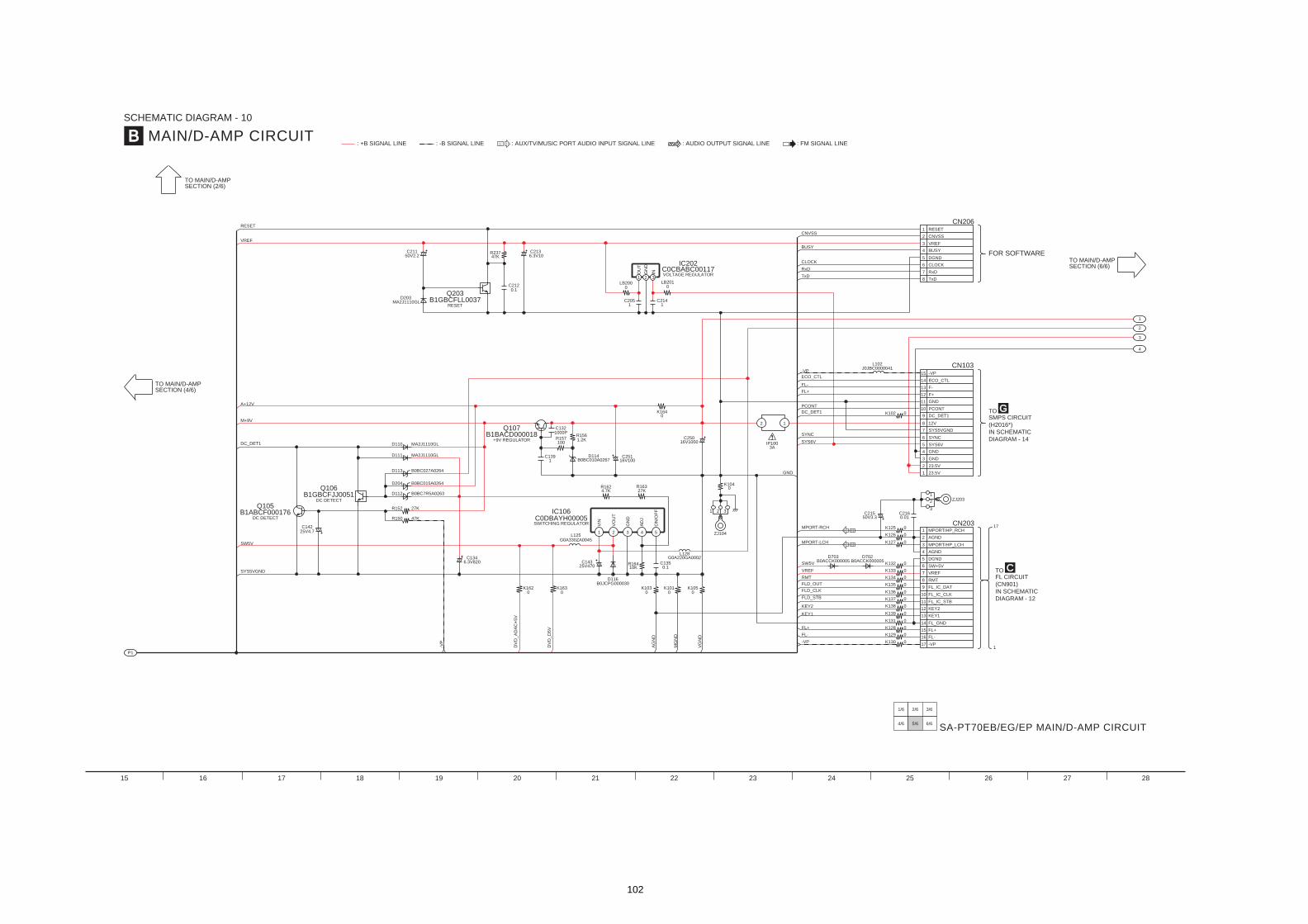
102
1
2
3
4
TO MAIN/D-AMPSECTION (4/6)
TO MAIN/D-AMPSECTION (2/6)
TO MAIN/D-AMPSECTION (6/6)
SA-PT70EB/EG/EP MAIN/D-AMP CIRCUIT
2/6 3/6
5/6
1/6
4/6 6/6
MAIN/D-AMP CIRCUIT
SCHEMATIC DIAGRAM - 10
B
CTOFL CIRCUIT
(CN901)
IN SCHEMATIC
DIAGRAM - 12
GTOSMPS CIRCUIT
(H2016*)
IN SCHEMATIC
DIAGRAM - 14
17
1
: +B SIGNAL LINE : -B SIGNAL LINE : AUX/TV/MUSIC PORT AUDIO INPUT SIGNAL LINE : AUDIO OUTPUT SIGNAL LINE : FM SIGNAL LINE
22 23 24 25 26 27 28
DC_DET1
PCONT
SYNC
R16327K
0K102
0K104
FL+
SYS6V
321
ZJ104
10KR164
L128G0A220GA0002
0.1C135
42 3 5
116000030
K1050
K1010
FL-
ECO_CTL
L102J0JBC0000041
8
9
13
11
10
12
2
3
1
5
7
6
4
15
14
CN103
12
3AIP100
C25016V1000
K1640
A+12V
-VP
16V100C251
MPORT-RCH
MPORT-LCH 0K127
VREF
SW5V
0K125
0K126
-VP
FL- 0K129
FL+
0
K128 0
K131
0K130
FLD_OUT 0K135
FLD_STB
FLD_CLK
RMT 0K134
KEY1
KEY2
0K137
0K138
0K139
0K136
K132 0
D703B0ACCK000005
D702B0ACCK000005
0K133
3
2
1ZJ203
6
5
8
9
11
12
10
14
15
13
7
2
1
4
3
17
16
CN203
C21650V3.3C215
M+9V
MG
ND
0.01
FL_IC_CLK
KEY2
FL_IC_STB
VREF
RMT
FL_IC_DAT
AD
J
ON
/OF
F
23.5V
GND
SYNC
SYS6V
GND
23.5V
12V
F+
GND
PCONT
SYS5VGND
DC_DET1
FL+
-VP
FL-
FL_GND
KEY1
GN
D
VO
UT
F-
ECO_CTL
-VP
AGND
MPORT/HP_RCH
AGND
MPORT/HP_LCH
DGND
SW+5V
VG
ND
K1030
AG
ND
GND
5
6
1
3
4
2
8
7
CN206
FOR SOFTWARE
CNVSS
VREF
C2051
C2141
LB2000
LB2010
D203MA2J1110GL
C21150V2.2
C2120.1
Q203B1GBCFLL0037
C2136.3V10
R23747K
BUSY
VREF
CNVSS
DGND
CLOCK
RESET
TxD
RxD
BUSY
CLOCK
TxD
RxD
RESET
RESET
VOLTAGE REGULATOR2 31
IC202C0CBABC00117
INOU
T
GN
D
P1
15 16 17 18 19 20 21
R1624.7K
DV
D_A
DA
C+
5V
6.3V820C134
L125G0A330ZA0045
SW5V
1
C0DBAYH00005SWITCHING REGULATOR
IC106
25V470C143
DB0JCPG
B0BC7R5A0263D112
B0BC015A0264D204
B1ABCF000176Q105
C14225V4.7
K1620
DV
D_D
5V
K1630
-VP
R150 47K
R152 27K
B1GBCFJJ0051Q106
Q107B1BACD000018
DC_DET1
B0BC027A0264D113
MA2J1110GLD111
MA2J1110GLD110
1C139 D114
B0BC010A0267
1000PC132
1.2KR156
R157100
SYS5VGND
VIN
DC DETECT
DC DETECT
+9V REGULATOR
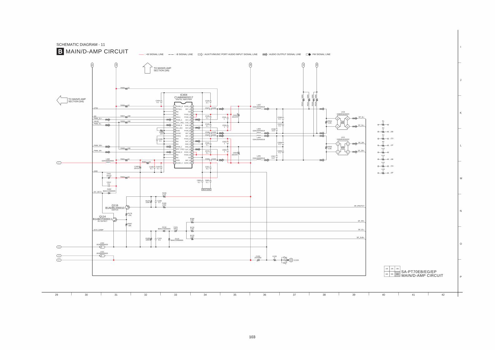
103
AA
AD
AC
AB
P1
TO MAIN/D-AMPSECTION (5/6)
TO MAIN/D-AMPSECTION (3/6)
SA-PT70EB/EG/EP MAIN/D-AMP CIRCUIT
2/6 3/6
5/6
1/6
4/6 6/6
B MAIN/D-AMP CIRCUIT
SCHEMATIC DIAGRAM - 11
: +B SIGNAL LINE : -B SIGNAL LINE : AUX/TV/MUSIC PORT AUDIO INPUT SIGNAL LINE : AUDIO OUTPUT SIGNAL LINE : FM SIGNAL LINE
36 37 38 39 40 41 42
I
J
L
M
N
P
O
K
K10
K3
...EB
...EG
...EP
0
K40
K90
K120
K14
...EB
...EG
...EP
0
K150
K200
C5531C574
0.1
SP_SR+
G0A100H00018
L405
G0A100H00018
L404
C5590.1
C5570.47
SP_SR-
C55425V470
PWM_SR+
R460 100
PWM_SR-
R461 10 C550 0.033
C5521 C558
0.1
R5055.6K
2
43
1
L411
G0B9R5K00003C4360.1
C5460.1
SP_FL+
SP_SUB+
SP_FR+
OTW
SD
IC404
DIGITAL AMPLIFIERC1AB00003217
C4340.1
VALID
R455 10
PWM_SL+
R456 10
100K
R530
100K
R532
100K
R531
100K
R529
C5260.1
SP_SL-
C527 0.033
C547 0.033
C5360.47
0.1C540
G0A100H00018L403
G0A100H00018L402
25V470C533
5.6KR504
2
43
1
L416
G0B9R5K00003
SP_SL+C5370.1
R458 100
R457 100
PWM_SL-
C5311
C5280.1
1C532
C5290.1
R45922K
C530 0.033
G0A200D00002L400
0K159C150
25V1000
SP_PROTCT
3
2
1
ZJ159
43
11
9
10
34
36
35
12 33
6
7
5
39
38
41
40
8 37
20
18
16
14
13
15
17
19
31
32
28
26
25
27
30
29
21 24
3
4
2
1
42
44
NC
OUT_C
BST_C
OUT_D
GND_C
GND_D
NC
OUT_A
BST_A
BST_B
GND_A
OUT_B
GND_B
BST_D
PVDD_D
PVDD_D
PVDD_A
PVDD_B
GVDD_A
PVDD_A
PVDD_C
NC
M2
NC
NC
M3
M1
GND
NC
VDD
VREG
AGND
PWM_B
PWM_D
PWM_C
SD(L)
PWM_A
OC_ADJ
GVDD_B
OTW(L)
RST_AB(L)
RST_CD(L)
1
2
3
4
29 30 31 32 33 34 35
R462 10
C5510.1
5.6KR184
5.6KR176
5.6KR175
0.1C802
0.1C803
R463 10
C4380.1
C4370.1
16V33
C441
C5120.1
C43916V10
GND
50V1C151
D119B0ACCK000005
220KR179 C158
0.1
100KR168 C153
0.1
R17847K
Q116B1ADBL000010
Q114B1ABCF000011
R58756K
220KR180
4.7KR236
D118B0ACCK000005
L421J0JKB0000020
L422J0JKB0000020
D402B0ACCK000005
DC_DET2
ECO_DAMP
HEATSINK
2322 GVDD_DGVDD_C
DC DETECT
SWITCH
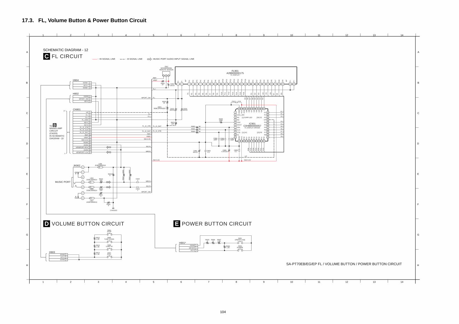
104
17.3. FL, Volume Button & Power Button Circuit
BBTOMAIN/D-AMP
CIRCUIT
(CN203)
IN SCHEMATIC
DIAGRAM - 10
17
C FL CIRCUIT
TON CIRCUIT
SCHEMATIC DIAGRAM - 12
SA-PT70EB/EG/EP FL / VOLUME BUTTON / POWER BUTTON CIRCUIT
: +B SIGNAL LINE : -B SIGNAL LINE : MUSIC PORT AUDIO INPUT SIGNAL LINE
A
B
C
D
1 2 3 4 5 6 7 8 9 10 11 12 13 14
8 9 10 11 12 13 14
A
B
D
E
F
H
G
C
C91550V22
P13
P15
P14
P6
P5
P7
P2
P1
P4
P3
P10
P12
P11
P8
P9
C91350V22
22KR923
P8
P7
C904100P
P9
C907100P
C906100P
G5
G3
G4
P6
G8
G7
G5
G4
G8
G6
G7
G1
P1
G2
G3
P4
P5
P2
P3
G9
C912 0.01
G9
G6
100KR905
21
5
6
3
1
2
4
19
9
7
8
16 17
11
10
12 151413 18 20
35374244 43 39 3841 40 36
33
22
31
29
27
24
23
26
25
28
30
32
34
IC901C0HBB0000057
G2
P16
G1
312 8 2621 232219 20 2524 28 292712 1310 14 16157 32
FL901A2BB00000175
68R902
68R904
R903 68
P14
P13
P16
P15
P11
P10
P12
6.3V220C905
0.1C909
-VP
R9221
3
2
H904
1.5KR907
R9081.2K
S901
S902
1
3
2
H902
R92410
B0BC2R4A0263D901
C93116V10
1
B3RAB0000081Z901
SW+3.3V
MLCH
RMT
6
5
8
9
11
12
10
14
15
13
7
2
1
4
3
CN901
F-
REMOTE SENSOR
F-
P3
P1
P11
P12
P10
G2
G3
G1
F+
F+
G6
G7
G4
G5
NP
G8
G9
NC
P15
P16
P13
P14
P9
P5
P6
P4
P8
P7
NP
P2
[23] P9STB [11] K2
DIN
DOUT
CLK P6
P7
P4
P5
P12
P17
P16
K1
GN
D
VC
C
P18
P13
P15
P14
P10
P11
P8
P1
P2
G1G3
P3
-VP
NC
GN
D
G9
G8
G1
0
VC
C
JOG_LED
[1] SURR LED
G5
G4
[34] G2
G7
G6
NC
OSC
RMTRMT
VREF
VREF
VREF
DGND
-VP
KEY2
DGND
FL+FL+
FL+
FL-FL-
FL-
DGND
KEY1
MPORT_SWMPORT_SW
DGND
AGND
FL_IC_STBFL_IC_STB
FL_IC_STB
KEY2
SW+3.3VSW+3.3V
FL_IC_CLK
FL_IC_DATFL_IC_DAT
FL_IC_DAT
HP/MPORT-RCH
KEY1
FL_GND
POWER
OPEN/CLOSE
1 4 5 6 9 11 17 18
2 3
47
FL DISPLAY DRIVER
FL DISPLAY
1
D VOLUME BUTTON CIRCUIT E POWER BUT
E
F
G
H
1 2 3 4 5 6 7
R954
6800
1C918R
953
6800
R919220
1C919R920
220
50V22C901
JK902
L904J0JBC0000014
R9290
J0JBC0000019L906
L905J0JBC0000014
0R930
L907J0JBC0000019
R9210
C9030.1
R9131.5K
R9122.2K
S904
S906
S905
R9060
R9150
S907R9141.2K
1
3
2
H901*
1
3
2
H903
SW+3.3V
MRCH
MRCH
MLCH
MPORT_SW
17
16
DGND
DGND
KEY1
KEY2
DGND
MPORT
CHASSIS
MUSIC PORT
AGND
HP/MPORT-LCH
PLAY
STOP
TUNE UP
TUNE DOWN
1
7
6
3
4
2
5
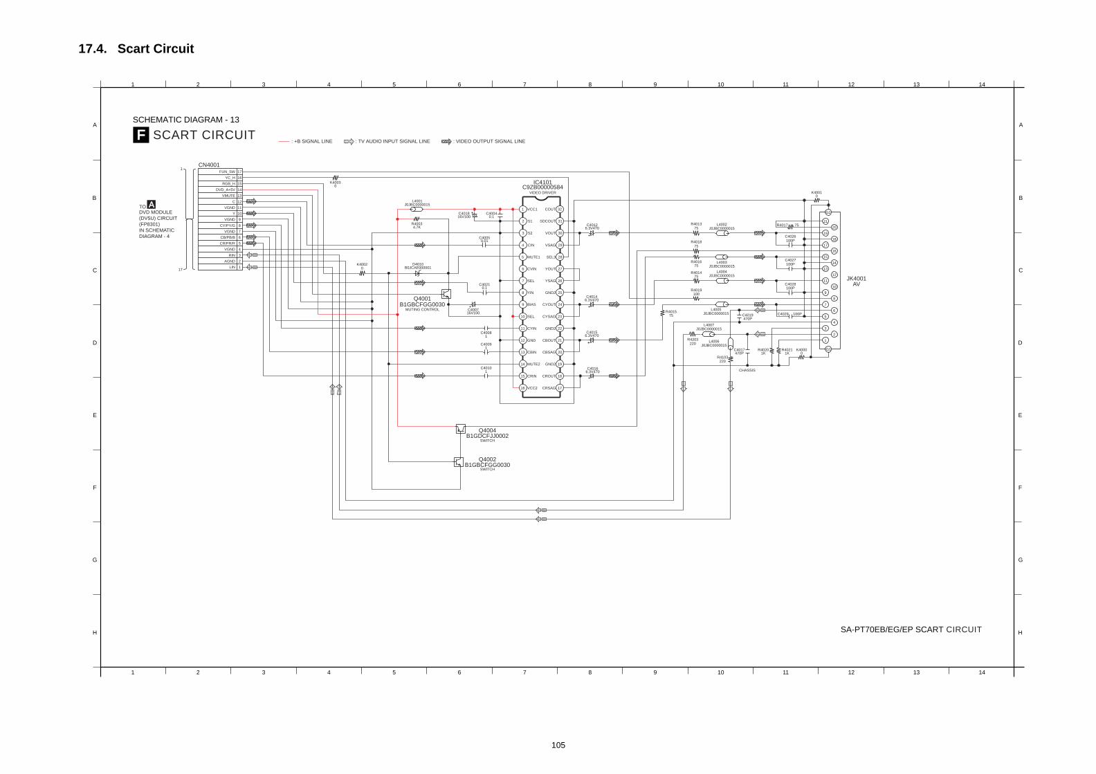
105
17.4. Scart Circuit
AATODVD MODULE
(DV5U) CIRCUIT
(FP8301)
IN SCHEMATIC
DIAGRAM - 4
17
1
F SCART CIRCUIT
SCHEMATIC DIAGRAM - 13
SA-PT70EB/EG/EP SCART CIRCUIT
: +B SIGNAL LINE : VIDEO OUTPUT SIGNAL LINE: TV AUDIO INPUT SIGNAL LINE
A
B
C
D
1 2 3 4 5 6 7 8 9 10 11 12 13 14
8 9 10 11 12 13 14
A
B
D
E
F
H
G
C
K4000
18
14
16
20
19
15
13
17
21
G2
8
10
4
2
6
12
9
5
1
3
7
G1
11
K4001
D4010B0JCAE000001
L4001J0JBC0000015
R4003
K4003
K4002
L4002J0JBC0000015
L4003J0JBC0000015
L4004J0JBC0000015
L4005J0JBC0000015
L4007J0JBC0000015
L4006J0JBC0000015
R401375
R4017 75C40126.3V470
6.3V470
6.3V470
6.3V470
R401875
100PC4026
C4027100P
R401475
R401675
100R4019
100PC4028
C4014
C40040.1
Q4001B1GBCFGG0030
C4005
C40210.1
C401816V100
6
5
8
9
11
12
10
14
15
13
7
2
1
4
3
17
16
CN4001
R401575
220R4203
C4019470P
100PC4029
R4103220
R4021R4020470P
C4017
C40081
16V100C4007
C4015
C40091
C4016
26
25
27
28
17
18
20
22
24
23
21
19
8
7
5
6
10
9
13
11
12
3
1
2
30
32
31
4 29
IC4101
CHASSIS
SEL CYSAG
UTE2
RIN
C2
CYIN
GND
CBIN
GND2
CROUT
CRSAG
GND2
CBOUT
CBSAG
CVIN
CIN
MUTE1
YIN
SEL
BIAS
VCC1
S1
S2
SEL3
VOUT
VSAG
GND2
YOUT
YSAG
SDCOUT
COUT
CYOUT
VGND
C
Y
YC_H
RGB_H
DVD_A+5V
FUN_SW
VGND
VMUTE
VGND
LIN
RIN
AGND
VGND
CR/PR/R
CB/PB/B
CY/PY/G
0
0
01K 1K
0.01
4.7K
0
C9ZB00000584VIDEO DRIVER
JK4001AV
MUTING CONTROL
E
F
G
H
1 2 3 4 5 6 7
Q4002B1GBCFGG0030
Q4004B1GDCFJJ0002
C40101
16
15
14 M
C
VC
SWITCH
SWITCH
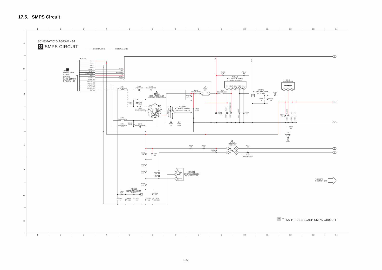
106
17.5. SMPS Circuit
P1
3
4
2
1
SA-PT70EB/EG/EP SMPS CIRCUIT2/21/2
SMPS CIRCUIT
SCHEMATIC DIAGRAM - 14
TO SMPSSECTION (2/2)
G: +B SIGNAL LINE : -B SIGNAL LINE
BTOMAIN/D-AMP
CIRCUIT
(CN103)
IN SCHEMATIC
DIAGRAM - 10
A
B
C
D
1 2 3 4 5 6 7 8 9 10 11 12 13 14
8 9 10 11 12 13 14
31 2
B0HBSM000054D5802
2.2KR5843
C5801
0.0
1
0.0
1
2.2KR5834
25V
1000
C5808
R5842
330
C5839
D5725
B0BC6R2A0266
IC5801C0DAEMZ00001
SHUNT REGULATOR
R57301K
3 21
ZJ5802
0.01C5800
R58082.2K
R5807330
R5809330
4
3
1
2
B3PBA0000454FEED BACK
PC5720
47K
R2914
30KR2906R2905
4.7K
G0C390JA0055L2910
1 2
1AFP2901
C290016V33
D2908
B0EAMM000057MAZ8240GHL
D2909
4.7KR2900
421 3 5
C0DBAYH00005SWITCHING REGULATOR
IC2900
SYS5V
SYNC
R2902
L2915J0JBC0000041
L2916C2912
D2906
B0B
C036A
0264
D2901
L2914
J0JBC0000041
8
9
13
11
10
12
2
3
1
5
7
6
4
15
14
H2016*
B0EAMM000057D2903
5 3
4
8
7
6 2
1
9
T2900G4D1A0000118
SWITCHING TRANSFORMER
C2903
35V33
C29080.1
R2907
3.9
K
B0JC
PG
000030
D2907
25V
100
C2907
16V820C2906
L2900G0A330ZA0045
Q2900B1BABK000001
PCONT
C290200P
Q5841B1GBCFGG0030
DC DETECT
1
C5843
-26V
3.9V(FL2)
ECO CTL
VDD
VDD
SYS5V
GND
GND
PCONT
DCDETDCDET
DC
DE
T
SYNC
12VGND
12V12V
12
V
SYS5VGNDSYS5VGND
3.9V(FL1)
VIN GND ON/OFFADJVOUT
POWER SAVE CONTROL
E
F
G
H
1 2 3 4 5 6 7
R58042.7K
R58032.7K
A
R
3
2
C1
R580615K
C58180.1
R5866100K
C58700.01
R58654.7K
C58640.1
22R5829
6.3V2200C5820
R58012.7K
560R5817
Q5863B1ABCF000176
R580218K
C5810
0.1
47J0JBC000004116V100
B0JAME000029 56
SWITCH
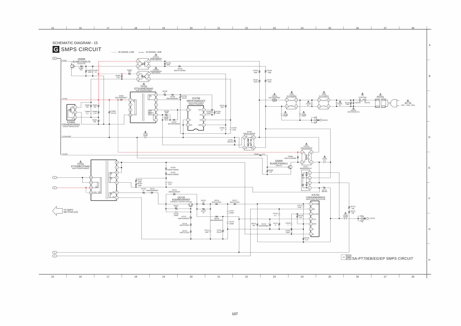
107
P1
SA-PT70EB/EG/EP SMPS CIRCUIT2/21/2
G SMPS CIRCUIT
SCHEMATIC DIAGRAM - 15
: +B SIGNAL LINE : -B SIGNAL LINE
15 16 17 18 19 20 21 22 23 24 25 26 27 28
22 23 24 25 26 27 28
A
B
D
E
F
H
G
C
SYS5VGND
4
3
1
2
B3PBA0000454FEED BACK
PC5799
B3PBA0000454SYNC SWITCH
PC5702
4
3
1
2
R5708820K
D5798B0EAMM000057
R579822
B0ECET000002D5730
C57061000P
R5786200K
D5793B0HAMP000094
2200PC5790
R572433K
400V68C5711
4
3
1
2
D5799B0EDKT000009
R57013.9M
DZ5701ERZV10V511CS
P5701
ZA5702 ZA5701
F1T2AH 250V
3
2ZJ5702
3
2
4
1
L5701ELF17N007A
L5702ELF18N006A
C5701
D4CAA5R10001TH5702
C57041000P
C5702
C57081000P
3
2
4
1
R5723
33K
3
2
4
1
D5701B0EBNR000015
4
3 1
2
K6B1AEA00003RY5701
C5703
D5899B0ACCK000005
50V10C5798
R5704
180K 180K
R5705
R5706
220K
R5898 4.7K
47KR5899
400V6.8C5799
15KR5797
470P
C5797
0.1
C5796
Q5899B1ABCF000011
R5707
220K
470KR5795C5795
1000P
7
8
5
1
2
4
3
IC5799MIP2F20MSSCF
SWITCHING POWERSUPPLY CONTROL
C5722
2200P
2200P
C5727
D5727MA2J1110GL
R57260.27
470PC5723
C57301
6
3
1
5
7
IC5701C0DAAMH00015SWITCHING REGULATOR
47KR5733 C5700
2200P 3
2
1
ZJ5700
R5732
100D5732
MAZ83000ML
C5747560P
K57210
0.1
C5725
D5896B0EAMM000057
SYS5V
A
R
3
2
C1
C0DAEMZ00001SHUNT REGULATOR
IC5899
C5899
10V220
R589339K
R589515K
R58924.7K
33KR5891
C58980.1
0.1C5897
SYNCB1ABCF000176
Q5898
R5886
INVERTER
100
100KR5887
330R5894
R58902.2K
9
10
7
8
2
1
6
4
ETS19AB2A6AGSUB TRANSFORMER
T5751
D
GND
FB
OLP/SS
VCC
S
OCP/BD
0.1
0.1
S
SD
FB
VDD
VCCD
TR
0.1 220V ~ 240V 50HzAC IN
5
3
4
2
1
SWITCH
3
4
2
1
TO SMPSSECTION (1/2)
15 16 17 18 19 20 21
B0EAKT000062
D5703
B0EAKT000061
D5700
100K
R5702
D5729B0EAMM000057
C5726
50V10
MA2J1110GLD5724
D5726MA2J1110GL
D5722
B0BC018A0267
D5723MA2J1110GL
1000PC5720
R5703
100K0.01
C5713
D5731B0EAMM000057
R572022
B0BC020A0267D5721
R572110K
B1BABG000007Q5720
8
14
12
13
15 2
1
7
5
ETS35BC2T6ADMAIN TRANSFORMER
T5701
R57222K
R57252K
220P
C5721
PCONT
+25V V1
V2
6
4
CURRENT LIMITING SWITCH
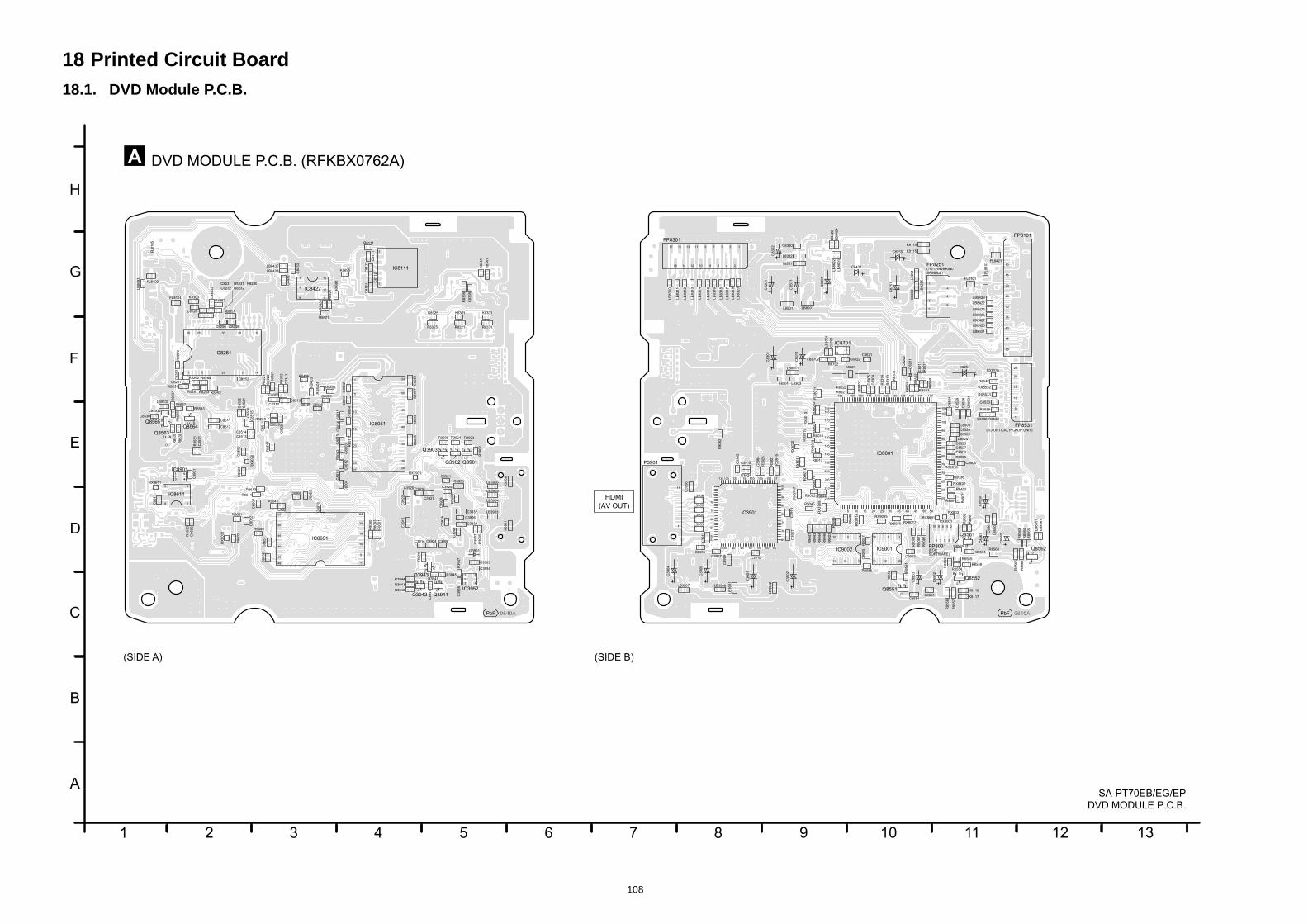
108
18 Printed Circuit Board18.1. DVD Module P.C.B.
17 8 9
F
G
H
10 1 12 13
A DVD MODULE P.C.B. (RFKBX0762A)
SA-PT70EB/EG/EP
DVD MODULE P.C.B.
E B)
0640A0640A
R8403
C8511
R8221
R8225
R8312
R8406
R8401
C8221
C8222
5C8226
C8313C8312
C8303
C8311
41
C8429 C8026
C8515
C8516C
8521
C8522
C8015
14
C8005
C8052
C8053
C8054
RX
8401
IC8051
C8057
C8056
C8051
LB8430
LB8423 C8433
C8432
R8421
R8404
IC8422
K8695
K8691
LB
8693
LB
8432
R8111
C8111
C8112
C8151
R8533LB8532
R8537
R8536
LB8530
C8530
Q8565
R8534
R9099
R8231 R8230C8231
C8232 R8232
R8252
C8258C8256
R8251
C8252
K8252R8263
R8264
IC8251
R8261
C8261
C8262
R8262
K8251
C8113
FL8102
K8325
R8325
K8321
R8321
K8331
R8331
K8335
R8335
K8341
R8341
C8024
K8100
IC8111
FL8105
FL8104
R8407
LB8011
C8011
R9085
C8301
IC8001
IC9002 IC9001FP8031
X8621
IC8701
RX
8011
RX
8012
RX
8013
RX
8014
RX
8015
RX
8016
RX
8017
RX
8018R
X8019
RX
9014
RX9015
RX9016 RX9017
R9043
R9044
R9046
R9023
R9048
R9086
R9087
R9088
RX8691RX8001
RX8031
C8502
C8527
C8523
C8524
C8525
C8504
C8529
C8528
R9055
C8304
C8305
L8301 R8313
R8314
R8011
R9083 R9084
R9045
R8621
R8622
C8622
C8621
LB
8701
C8701
R8311
L8303
C9002
R9007
R8013
R9036
R9049
RX9018
RX
3708
RX
8020
RX
3707
C8503
C9003
LB
8901
R8702
R8901
LB
8401
R9047
D8211
C8202
RX8402
R8402
L8251
C8255
C8257
C8251
C8260
FP8251
R8553 R8555
R8554
Q8552
R8557
R8556
C8552
R8558
R8559(FORSOFTWARE)
(TO OPTICAL PICKUP UNIT)
(TO TRAVERSE/SPINDLE)
R8551
R8552
C8553
C8554
Q8551C8551
L8550
C8550
R8561
R8563
R8565
R8564
Q8562R8568
R8567
R8566
C8562
C8563
C8564
Q8561
R8562
C8561
LB8421
LB8428
LB8427
LB8426
LB8425
LB8422
FL8101
FL8103
FP8101
L8501 LB8001
L8201
L8302
R8422
K8114
K8115
K8116
K8117
LB
8424
C8431
R8532C8532
R8539
C8533
RX8531
RX8533
LB
8551
LB
8561
FP8531
R8542
C8001
LB
8692
C3956
L3906
L3905
L3904
L3903
LB3908
K3905
C3906
C3904
LB3907
LB
3901
C3901
LB
3902
C3902
C3917
C3907
C3909
C3910
C3911
C3919
R3921
R3925
C3964
C3918
R3924
C3965
C3913
IC3901
R9082
C8501
C8201
C8320
C8302
LB
8315
LB
8320
LB
8314
LB
8319
LB
8313
LB
8318
LB
8312
LB
8317
LB
8311
LB
8310
LB
8691
LB
8531
C8505
R8211
C8211
RX8532R8503
R8504
R8501 R
8502
LB
8316
LB8702
P3901
C8526
FL8421
LB
8255
FP8301
LB8429
MI
OUT)
G
D
SB
C
B
C
E
B
C
E
B
C
E
B
C
E
PbF
1 5 10 15 20 25 30 35 40 45 50 54
55
60
65
70
75
80
85
90
95
100
105
108
109115120125130135140145150155162
163
165
170
175
180
185
190
195
200
205
210
216
1510
11 15 20
1510
11 15 20
15 3
10 2
7
4
9
68
1234
5
1
3
5
7
2
4
6
1
5
10
15
20
25
30
35
40
50
45
1
5
10
15
20
24
1
5
10
15
20
25
30
32
3335 40 45 50 55 60 64
65
70
75
80
85
90
9596
97100105110115120125128
19
1
15791117
246816
15
101214
313
28 25 20 15
141051
30
29
16
12
98
4
1
7
1
1
5
1045
50
54
1 2 3 4 5 6
A
B
C
D
E
(SIDE A) (SID
0640A0640A
IC8651
R8012
R8601
R8541
C822
C85
C8006
RX
9020
C8513
C8506
C8023
RX
8032
C8022
C8007
C8021
C8020
C8018
C80
C8013
C8003
C8012
C8016
C8004
R9042
R8001
R8003
R9080
R9041
R9040
C8651
C8652
C8055
C8514
C8901IC8901
RX8611
IC8611
C8611
C8602
R9038
R8538Q8563
R8535
Q8564
C8531
R8531
C8512
R8602
K3911
K3909
R3903
LB3906R
3902
Q3901
D3901
LB3905
LB3904
LB3903
R3904R3906
Q3902
Q3903
R3907
R3905
K3903
R3945Q3943
R3946
R3944
R3943
Q3942
C3941R3942
R3941
Q3941
C3954R3947
C3955 IC3952
R8611
R8613
RX3901
C3915
C3922
C3920 C3916
C3927
C3921
C3923
C3925
C3928
C3932
C3926
C3929
C3940
C3930
C3914 C3924 C3908
R3901
HD
(AV
E
BC
E
B
C
EB
C
E
G
D
S G
D
S B
C
E
G
D
S
PbF
123 4
5
8
5 4
1
1
5
10
15
2425
35
40
48
2030
45
15
20
2728
35
40
3025
5
4
1
2
3
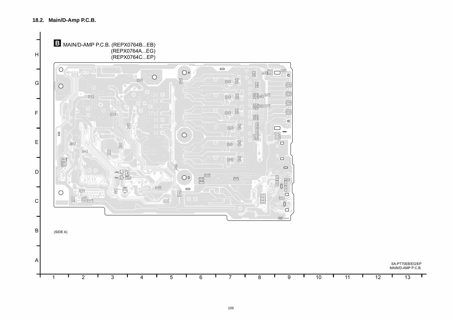
109
18.2. Main/D-Amp P.C.B.
17 8 9
E
F
G
H
10 1 12 13
B MAIN/D-AMP P.C.B. (REPX0764B...EB)
(REPX0764A...EG)
(REPX0764C...EP)
SA-PT70EB/EG/EP
MAIN/D-AMP P.C.B.
PbF
K141
K143
K142
K140
R500
R501
R502
R503
R504
R505
C473
C472
C487
C486
C502
C501
C522
C523
C537
C540
C558 C559
K157 C567
R532
R528
R527
R526
R525
R529
R530
R531
R175
R184
R176
C802K159
K105
R274
K101
C190
C182
C183
C184
C185
C186
C187
C188
C191
C192
C181
C189
K20...EP
K103
R203
C51
C59
L51
LB51
R51
R63
0644A0644A
1 2 3 4 5 6
A
B
C
D
(SIDE A)
C803
K116
C130
R276
R275
K131
K130
Q801
R280
K128
K129
R271
D203
R801
Q803 R802
Q802
D802
K14...EB
K15...EG
K12...PT70
D703
C216
B
C
E
BC
E
BC
E
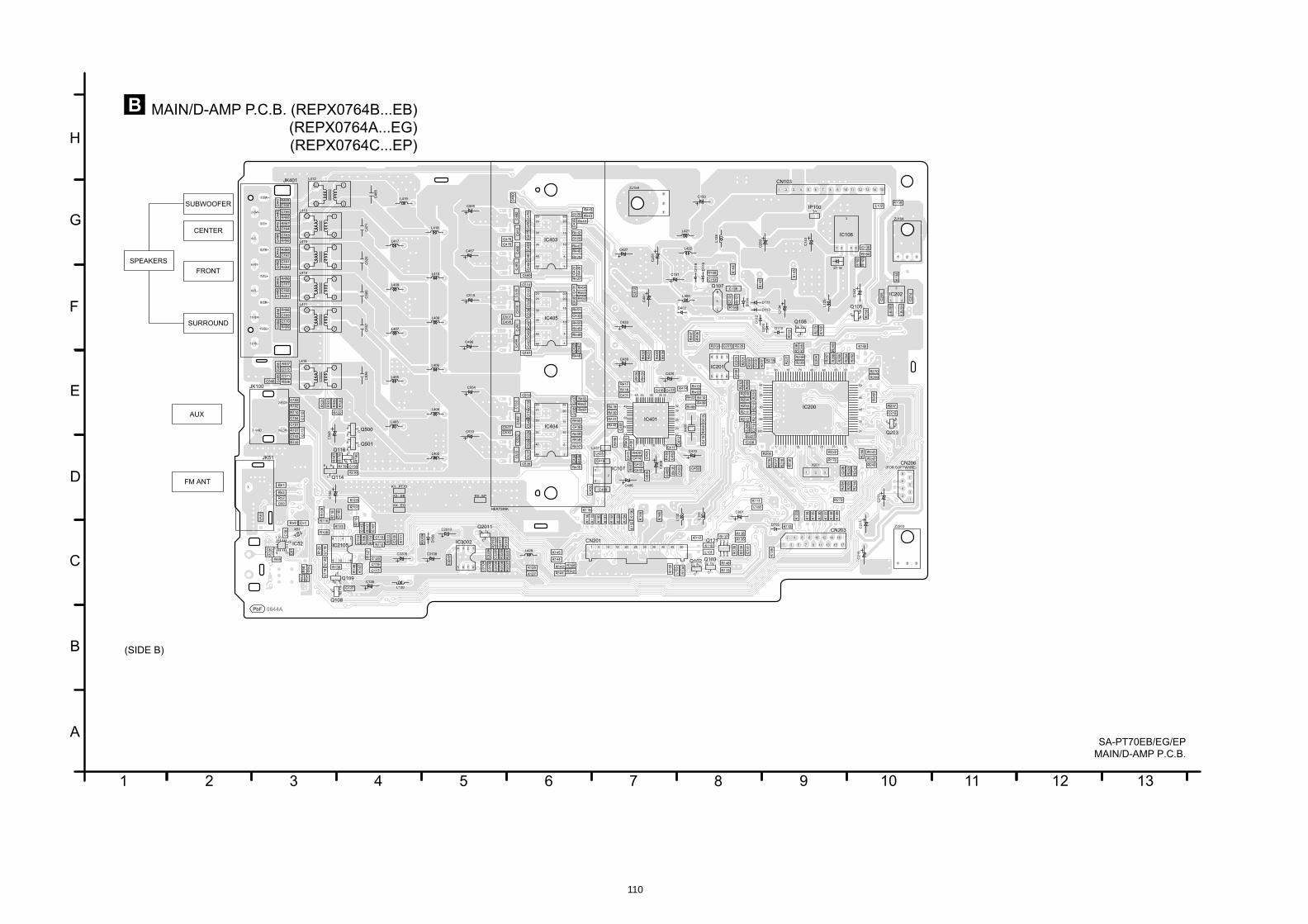
110
17 8 9
E
F
G
H
10 1 12 13
B
SA-PT70EB/EG/EP
MAIN/D-AMP P.C.B.
MAIN/D-AMP P.C.B. (REPX0764B...EB)
(REPX0764A...EG)
(REPX0764C...EP)
IC403
C461
C462
C463
C466
C477
C478
C480
C482
C490
C460
C479
C476
C470
C464
C492
C498
C507
C510
C481
C514
C516
C515 C
509
C508
C491
C494
C497
C493
IC405
C550
C551
C553
C552 C
574
546
L413
L414
L415
L416
L411
JK401 L412
JK100
C505
C467
C496
C554
C536
C471
C485
C500
C520
C557
L405
L403
L404
L409
L406
L407
L408
L417
L410
L419
L418
R522
R523
R520
R521
R524
C112
C104
R110
C101
C102
R102
R468C446
C166C447
C165
R469
R466C444 C163
C164
R467
C445
R464C442 C161
C162C443 R465
R497
C168
C449
C448
C167
R496
R499C454 C170
C169C450 R498
R506C455 C171
C172
R507
C456
C566
C519
R401
R400
R404
L103
R140
L101
R134
K110
K112
IC401
R418
R417
R424
R423 C420
C417C416R414
R413
C413
C415
R419
R430
C421
C406
C407
R495
C400
C401
C402
C414
C403
R402
C404
C408
C412
R436
R435
C452
IC107
32
R431
R412
R410
R409R408
X400
C439
C405
K153
K154
K152
K155
L132
C409
L131
R422
R421
R420
R416
C423
R428
R427
R429
R440
R441
C424
R442
R443
R444
C426
C425
R445
C427
C433
R454
C431
C432 R452
R453
R451
C430
R450
R449
R448
R446
R447
C429
R463
C437
C438
R461
R462
R460
C512
C411
C441
L102
3A
R221
Q107
D118
D119
C153
R168
C139
R157
R156
D114
C132
R172
L128
C151
L422
L421
C251
L125
C250
CN203
C214
C205
LB
200
LB
201
IC202
K102
IC106
D110
D112
D111
D204
Q106
Q105
D116
R162
R164
R163
C135
R219
R220
R207
L400
R406
R407
R239 C204
K133
K139
K136
K132
K134
K138
K137
K135
K126
K111
R237
Q203
C212
CN206(FOR SOFTWARE)
IC201
IC200
R272
R273
C131
R139
Q121 R135R137
R136
R138
R152
X201
R133
R146Q102 Q103
R214
R262
L100
C801
R242
C203
R263
C211
C213
C200
R201
C202
R200
C201R202
R267
R266
R265
R264
R269
R270
R249
R206
R246
R245
R247
R234
R233
R232
R231
R213
C210
C209
R212
R208
R209
R210
R211
C207
C208
R243
R244
R241
R240
R238
C206R
230
R218
R217
R216
C150
C410
C453
C451
D402D113
R222
R205
R204
CN103
K160
K158
IP100
C142
C134
D702
C143
K166
K162
K163
K164
K165
C215
ZJ104
ZJ159
ZJ203
K104
R403
K156
R150
SUBWOOFER
CENTER
FRONT
SURROUND
AUX
SPEAKERS
B
C
EB
C
E
BC
E
BC
E
B
C
E
B
C
E
44
40
35
30
25
23 22
20
15
10
5
1
44
40
35
30
25
23 22
20
15
10
5
1
30
25
23 22
20
15
2-RCH
4 3
2 1
4 3
2 1
4 3
2 1
4 3
2 1
4 3
2 1
1-SW+
12-SL-
11-SL+
10-SR-
9-SR+
8-FL-
7-FL+
6-FR-
5-FR+
4-C-
3-C+
2-SW-
4 3
2 1
5045403530252015
1 5 10 16
17
20
25
30
32
3335404548
49
55
60
64
2
1
4
3
6
5
8
7 9
16
17
14
15
12
13
10
11
1
2
3
54
3
21
2
1
4
3
6
5
7
8
3 2 1
4 5 6
1 32
124 3
5 6 7 8
1 5 10 15 20 25 30
51556065707580
31
35
40
45
5081
85
90
95
100
1514131211101 2 3 4 5 6 7 8 9
321
3
2
1
321
1 2 3 4 5 6
A
B
C
D
(SIDE B)
PbF
R143 R144
R141R142
K125
K127
C527
C530
C547
C526
C
C532
C531
C529
C528
IC404
C126
C115
R117
C107R
115
R105
R107
R108
R106
R116
C108
R118
C116
C123
R130
R125
C119
C120
R111
C105C113
R113
R114
C114
C106
R112
C118
C117
IC2105
C127 L120
R126
Q109
Q108
R127
R103
K147
C533
L402
R180
C158R179
Q116
R178
R587
Q114
C548
Q500
Q501
C103
R109
C111R101
R236
CN201
K113
K115
K114
L425
C418
C419
L426
R4
K150
K151
K144
K145
C436
R459
R458
R457
R455
R456
C434
L427
K3...EB
K4...EG
K9...EP
K1...PT70
C3108
C136
C3208
Q2011C2010
L428
IC3002
C3106
C3105
R3108
R3107
R3207
R3208
C3205
C3206
C3207
R2010
C2011
R2012
D106
C3104
R3209
C57
C60
IC52
R52
R53
R54
R55
R56
R59
X51
R61
R62
VA
51
C61C62
R64
R57
JK51
C58
FM ANT
0644A0644A
HEATSINK
BC
E
BC
E
B
C
EB
C
E
B
C
E
B
C
E
BC
E
44
40
35 10
5
1
16129
8 4 1
3-LCH1-GND
1051
1
2
3
124 3
5 6 7 8
20
15
116
5
1
1
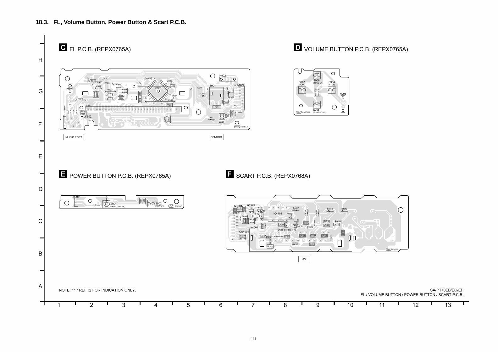
111
18.3. FL, Volume Button, Power Button & Scart P.C.B.
17 8 9
E
F
G
H
10 1 12 13
C FL P.C.B. (REPX0765A) D VOLUME BUTTON P.C.B. (REPX0765A)
ART P.C.B. (REPX0768A)
SA-PT70EB/EG/EP
FL / VOLUME BUTTON / POWER BUTTON / SCART P.C.B.
0648A0648A
0645AA0645AA
0645AB0645AB
IC4101
C4017L4007 R4020
K4000
4203
C4029 L4005
R4015
C4019
L4006
4103
R4019
C4028
R4014
L4004
C4027
L4003
R4016
R4018
C4026
L4002
R4013
R4017
K4001
C4010
C4009
C4008 C4004
L4001
Q4002
C4005
C4021
Q4001
D4010
R4003
K4002
W782
W780 W781
W783
W784
R4021
JK4001
N4001
C4012
C4014
C4015
C4016C4007
C4018
W751
W752
AV
MUSIC PORT SENSOR
R902
R903
R904
R905
R919
R920
R921
R922
C903
C904
C906
C907
C909
C912
R929
R930
C931
IC901
L904
L905
L906
L907
D901
R923 R924
W921
W923
W924
C918
R953
C919
R954
C901
C905
C913
C915
H902
JK902
Z901H904
W908
W907
W910
W909W904
W900
W903
W902
W905
W901
W912
W906
W911
CN901
FL901
W915
R912
R913
R914
H903
S904(STOP)
S905(TUNE DOWN)
S906(TUNE UP)S907
(PLAY)
B
C
EB
C
E
PbF
PbF
PbF
21
20
19
18
17
16
15
14
13
12
119
102
1
4
3
6
5
8
7
1 4 8 12 16
1720242832
13 2
7
6
5
4
3
2
1
13 2
1
3
2
21
43
65
87
9
1617
1415
1213
1011
14567893132 229 28 27 26 25 24 23 22 21 20 19 18 17 16 15 14 13 12 11 10
1
3
2
1
11
12
22 23
6
28
33
34
17
39
44
1 2 3 4 5 6
A
B
C
D
E POWER BUTTON P.C.B. (REPX0765A) F SC
NOTE: " * " REF IS FOR INDICATION ONLY.
0645AC0645AC
R
R
Q4004
K4003
C
S902(POWER)
S901(OPEN / CLOSE)
R915
R908
R907R906H901*
B
C
EPbF
12
34
67
9
5
8
1716
1514
1312
1110
1
3
2
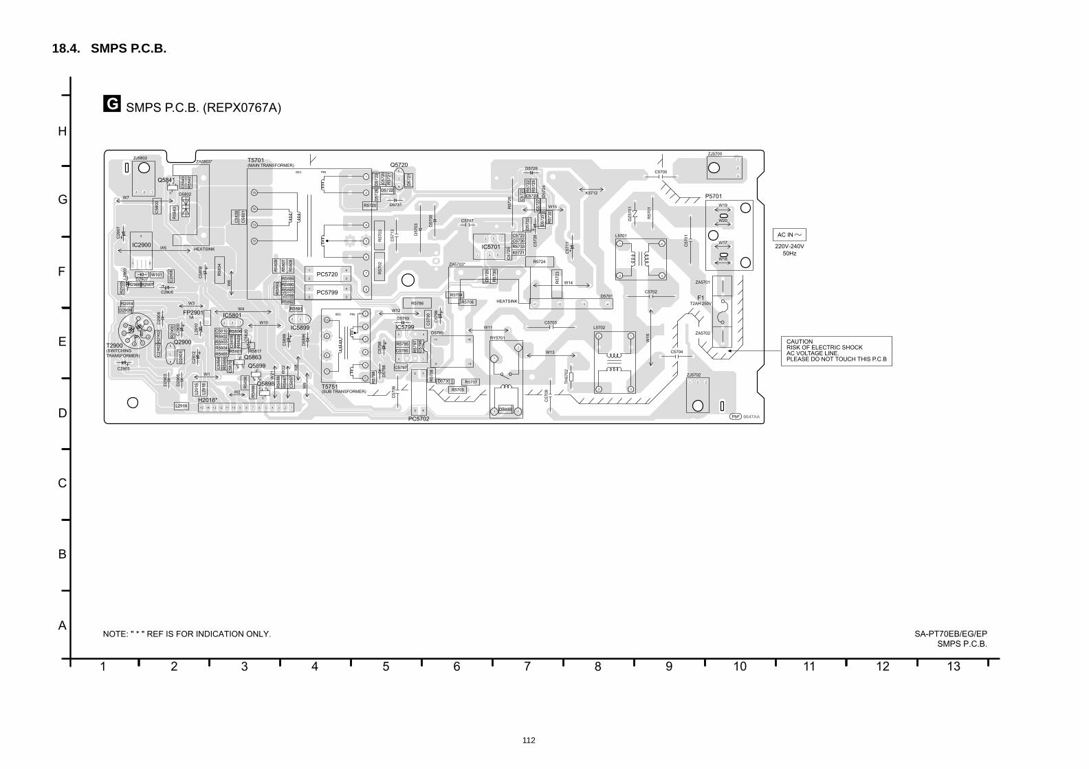
112
18.4. SMPS P.C.B.
17 8 9
E
F
G
H
10 1 12 13
G SMPS P.C.B. (REPX0767A)
SA-PT70EB/EG/EP
SMPS P.C.B.
0647AA0647AA
2902
C2908
C5720
C5721
C5722
C5723
C5725
C5727
C5730
C5790
C5795 C5796
C5800
C5801
C5810
C5818
C5839
C5843
C5898
1
D2909
D5721
D5722
D5723
D5724
D5725
D5726
D5727
D5732
D5799
9
FP29011A
IC2900
K5721
PC5720
PC5799
Q5841
R2900
R2902
R2905
R2906 R2907
R2914
R5702
R5703
R5704
R5706
R5720
R5721
R5722
R5723
R5724
R5725
R5730
R5732
R5733
R5786
R5795
R5797
R5802
R5803
R5804
R5806
R5807
R5808
R5809
R5817
R5829
R5834
R5842
R5843
R5890
R5891
R5892
R5893
R5894
R5895
R5801
D2907W101
C2900
C2906
C2907
2
C5700
C5701
C5702
C5703
C5708
C5711
C5713
C5726
C5747
C5798
C5799
C5808
C5820
C5899
D2908
D5700
D5701
D5703
D5729
D5731
D5793
D5896
DZ
5701
IC5701
IC5799
IC5801
IC5899
K5712
L2900
L2910
L5701
L5702
P5701
Q2900
Q5720
R5701R
5726
RY5701
T2900
T5701(MAIN TRANSFORMER)
TH
5702
ZA5701
F1T2AH 250V
ZA5702
ZJ5700
ZJ5702
ZJ5802
W10
W20
W17
W3
W4
W6
W11
W12
W14
W15
W13
W5
ZA5703*
W19
W18
W7
ZA5803*
HEATSINK
HEATSINK
D5802
C5704
W16
(SWITCHING
220V-240V
50Hz
AC IN
CAUTIONRISK OF ELECTRIC SHOCKAC VOLTAGE LINE.PLEASE DO NOT TOUCH THIS P.C.B
B
C
E
2 3 12 3 1
B
B
C
E
PRI
PRI
SEC
SEC
PbF
+1 -4~3~2
7
6
5
4
3
1
5 812
3 4
9
8
7
6 5
4
3
2
1
15
14
13
12
8
6
4
2
1
5
7
10
9
1
2
3
4
3
2
1
321
3 2 1
5
3
1
+1 ~4
4
32
1
4
32
1
4
2
1 4
2 3
1 2 3 4 5 6
A
B
C
D
NOTE: " * " REF IS FOR INDICATION ONLY.
C
C5864
C5870
C5897
D290
D5730
D589L2914
L2915
L2916
PC5702
Q5863
Q5898
Q5899
R5705
R5707R5708
R5798
R5865
R5866
R5886
R5887
R5898
R5899
C5797C2903
C291
C5706
D2903
D2906 D5798
T5751(SUB TRANSFORMER)
W8
W9
W2
W21 W
22
TRANSFORMER)
H2016*
W1
B
C
E
B
C
E
B
C
E
C
E14
7
8
6
5
43
2 1
-2 ~3
3
1
15 1234567891011121314
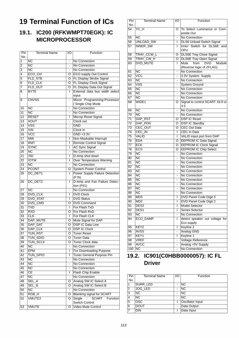
19 Terminal Function of ICs19.1. IC200 (RFKWMPT70EGK): IC
MICROPROCESSOR
19.2. IC901(C0HBB0000057): IC FL Driver
Pin No.
Terminal Name I/O Function
1 NC - No Connection2 NC - No Connection3 NC - No Connection4 ECO_Ctrl O ECO supply Out Control5 FLD_STB O FL Display Strobe Signal6 FLD_CLK O FL Display Clock Signal7 FLD_OUT O FL Display Data Out Signal8 BYTE I External data bus width select
input9 CNVSS - Micon Programming-Processor
/ Single Chip Mode10 NC - No Connection11 NC - No Connection12 RESET I Microp Reset Signal13 XOUT - Clock out14 VSS - GND15 XIN - Clock In16 VCC - GND +3.3V17 NMI I Non Maskable Interrupt18 RMT I Remote Control Signal19 SYNC I AC Sync Signal20 NC - No Connection21 /SD I D-Amp shut down22 /OTW I Over Temperature Warning23 NC - No Connection24 PCONT O System Power Control25 DC_DET1 I Power Supply Failure Detection
(F76)26 DC_DET2 I D-Amp and Fan Failure Detec-
tion (F61)27 NC - No Connection28 DVD_CLK I DVD Clock29 DVD_STAT I DVD Status30 DVD_CMD O DVD Command31 TXD I For Flash TxD32 RXD O For Flash RxD33 CLK I For Flash CLK34 DAP_MUTE O Mute Signal for DAP35 DAP_DAT O DSP IC Data Line36 DAP_CLK O DSP IC Clock37 TUN_RST O Tuner Reset38 TUN_SDIO O Tuner Data39 TUN_SCLK O Tuner Clock data40 NC - No Connection41 EPM I For Downloading Purpose42 TUN_GPIO I Tuner General Purpose Pin43 NC - No Connection44 NC - No Connection45 NC - No Connection46 CE I Flash Chip Enable47 NC - No Connection48 SEL_A O Analog SW IC Select A49 SEL_B O Analog SW IC Select B50 NC - No Connection51 RGB_H O Blanking signal for SCART 52 VMUTE2 O Single : SCART Function
Switch Control53 VMUTE O Video Mute Control
54 YC_H O To Select Luminance or Com-posite Out
55 NC - No Connection56 UNLOAD_SW I DLS6 Unload Switch Signal57 INNER_SW I Inner Switch for DLS6E and
OPU58 TRAY_CCW_L O DLS6E Tray Close Signal59 TRAY_CW_H O DLS6E Tray Open Signal60 DVD_MUTE I Mute from DVD Module
(Reverse logic of ZFLAG)61 NC - No Connection62 VCC - 3.3V System Supply 63 NC - No Connection64 VSS - System Ground 65 NC - No Connection66 NC - No Connection67 NC - No Connection68 WIDE1 O Signal to control SCART 16:9 or
4:369 NC - No Connection70 NC - No Connection71 DAP_RST O DSP IC Reset72 DAP_PDN O DSP IC Standby73 CEC_OUT O CEC Out Data74 CEC_IN I CEC In Data75 VALID I VALID input port from DAP76 EDA O EEPROM IC Data Signal77 ECK O EEPROM IC Clock Signal78 ECS O EEPROM IC Chip Select79 NC - No Connection80 NC - No Connection81 NC - No Connection82 NC - No Connection83 NC - No Connection84 NC - No Connection85 NC - No Connection86 NC - No Connection87 NC - No Connection88 NC - No Connection89 MD3 I DVD Panel Code Digit 390 MD2 I DVD Panel Code Digit 291 DES2 I Model Selector92 DES1 I Series Selector93 NC - No Connection94 ECO_DAMP I detect speaker out voltage for
Eco supply95 KEY2 I Keyline 296 AVSS - Analog GND 97 KEY1 I Keyline 198 VREF - Voltage Reference99 AVCC - Analog +5V Supply100 NC - No Connection
Pin No.
Terminal Name I/O Function
1 SURR_LED - NC2 JOG_LED - NC3 NC - NC4 NC - NC5 OSC I Oscillator Input6 DOUT - Data Output7 DIN I Data Input
Pin No.
Terminal Name I/O Function
113
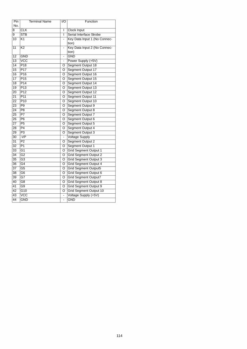
8 CLK I Clock Input9 STB I Serial Interface Strobe10 K1 - Key Data Input 1 (No Connec-
tion)11 K2 - Key Data Input 2 (No Connec-
tion)12 GND - GND13 VCC - Power Supply (+5V)14 P18 O Segment Output 1815 P17 O Segment Output 1716 P16 O Segment Output 1617 P15 O Segment Output 1518 P14 O Segment Output 1419 P13 O Segment Output 1320 P12 O Segment Output 1221 P11 O Segment Output 1122 P10 O Segment Output 1023 P9 O Segment Output 924 P8 O Segment Output 825 P7 O Segment Output 726 P6 O Segment Output 627 P5 O Segment Output 528 P4 O Segment Output 429 P3 O Segment Output 330 -VP - Voltage Supply31 P2 O Segment Output 232 P1 O Segment Output 133 G1 O Grid Segment Output 134 G2 O Grid Segment Output 235 G3 O Grid Segment Output 336 G4 O Grid Segment Output 437 G5 O Grid Segment Output538 G6 O Grid Segment Output 639 G7 O Grid Segment Output740 G8 O Grid Segment Output 841 G9 O Grid Segment Output 942 G10 O Grid Segment Output 1043 VCC - Voltage Supply (+5V)44 GND - GND
Pin No.
Terminal Name I/O Function
114
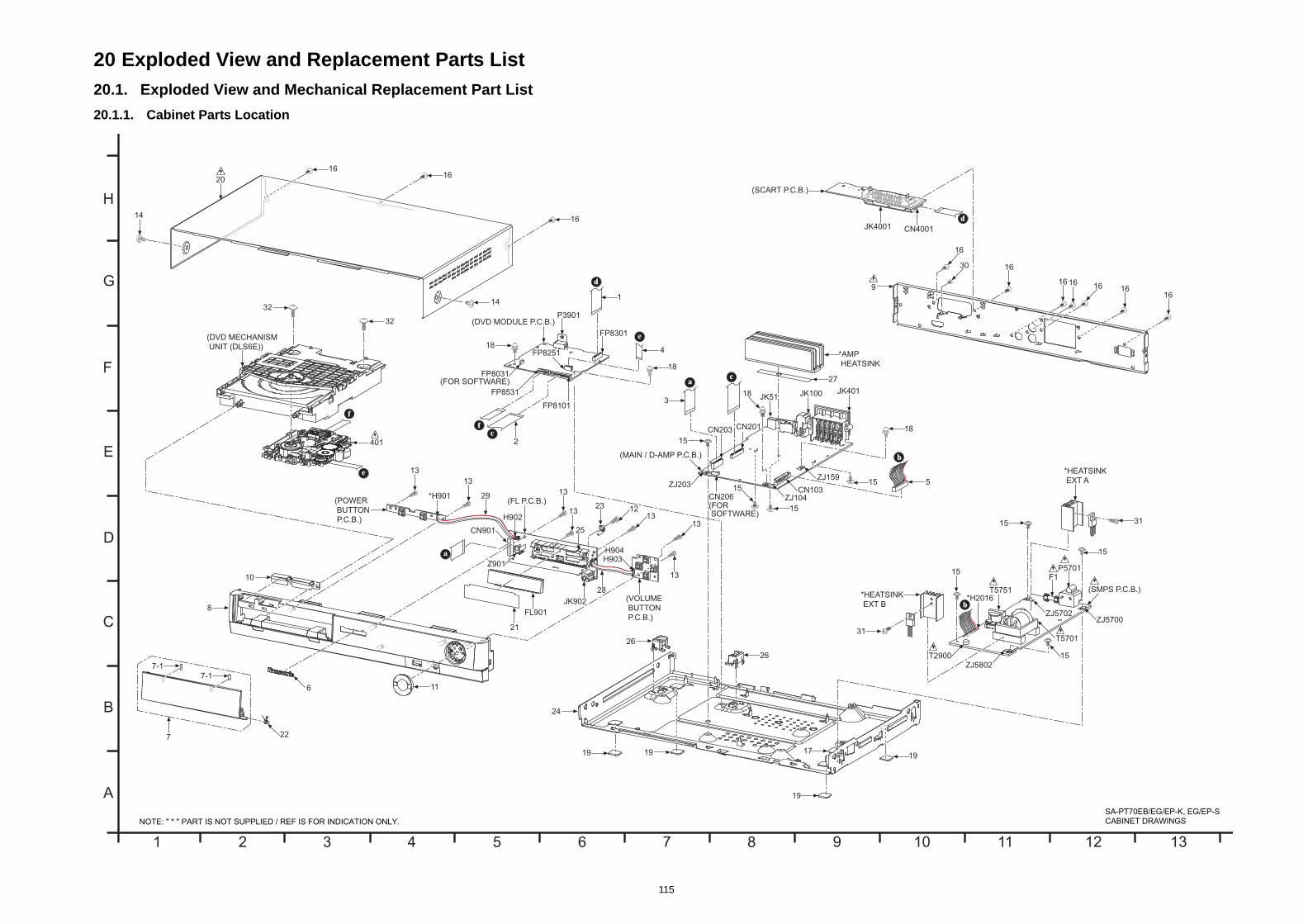
115
20 Exploded View and Replacement Parts List20.1. Exploded View and Mechanical Replacement Part List
20.1.1. Cabinet Parts Location
OLUME
UTTON
C.B.)
(SMPS P.C.B.)
(SCART P.C.B.)
IN / D-AMP P.C.B.)
(DVD MODULE P.C.B.)
ZJ5802
ZJ5702ZJ5700
ZJ203ZJ159
ZJ104
T5751
T5701
T2900
P5701
P3901
JK4001
JK401JK100JK51
*H2016
FP8531
FP8301
FP8251
FP8101
FP8031(FOR SOFTWARE)
F1
CN4001
CN206(FORSOFTWARE)
CN203 CN201
CN103
*HEATSINK
EXT A
*HEATSINK
EXT B
*AMP
HEATSINK
(DVD MECHANISM
UNIT (DLS6E))
32
32
31
31
30
27
26
20
19
19 19
18
18
18
18
17
1616
16
16
16
16 16 16 1616
15
15
15
15
15
15
15
15
14
14
1313
13
2
9
5
4
3
1
a
b
b
c
d
d
e
f
7 8 9
F
G
H
10 11 12 13
SA-PT70EB/EG/EP-K, EG/EP-S
CABINET DRAWINGS
(V
B
P.
(POWER
BUTTON
P.C.B.)
(MA
(FL P.C.B.)
Z901
JK902
H904H903
H902
*H901
FL901
CN901
401
29
28
26
25
24
23
22
21
19
13
13
13
13 1
11
10
8
7-1
7-1
7
6
2
a
c
e
f
1 2 3 4 5 6
A
B
C
D
E
NOTE: " * " PART IS NOT SUPPLIED / REF IS FOR INDICATION ONLY.
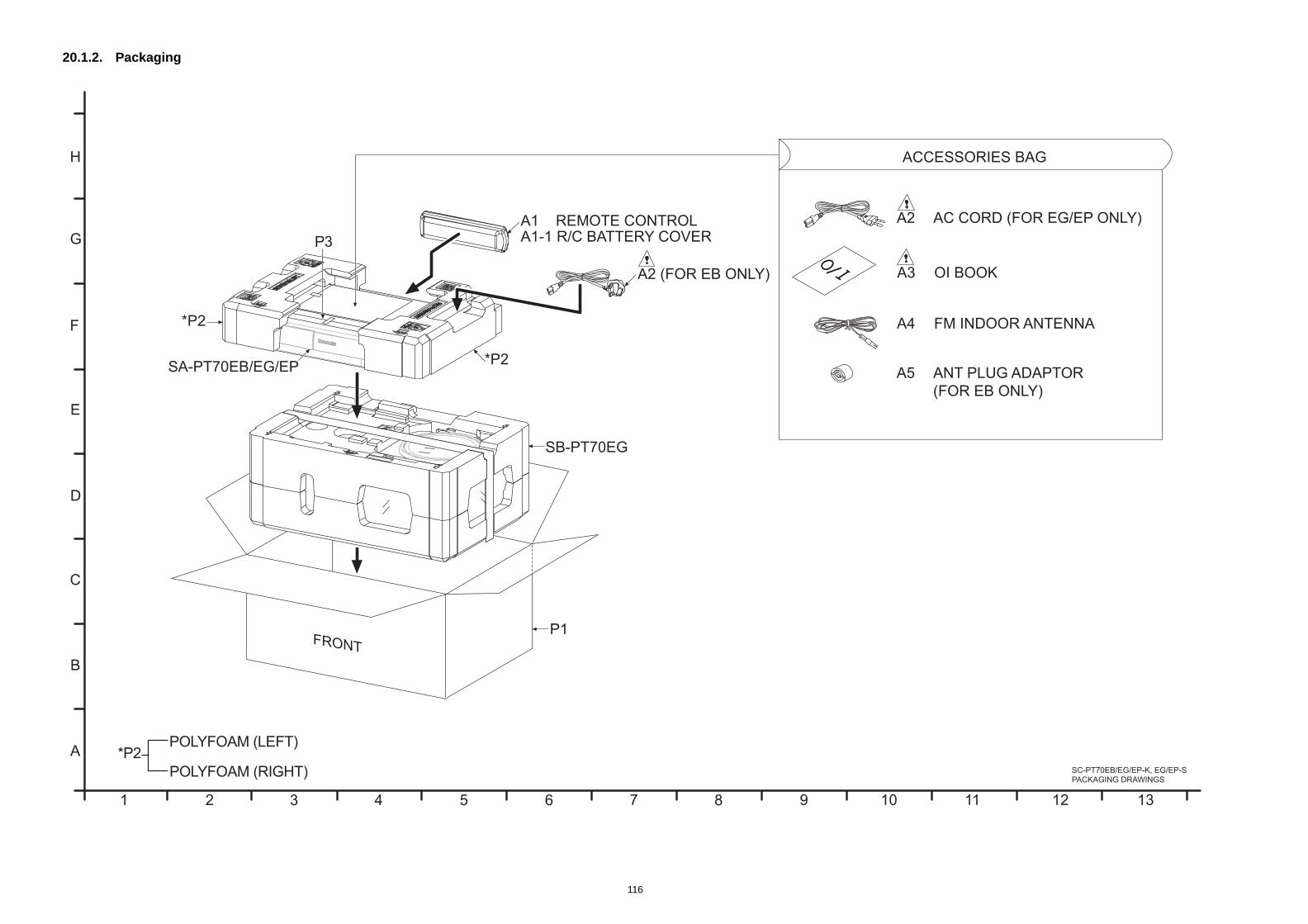
116
20.1.2. Packaging
G
SA-PT70EB/EG/EP
ACCESSORIES BAG
A5 ANT PLUG ADAPTOR
(FOR EB ONLY)
A4 FM INDOOR ANTENNA
A3 OI BOOKA2 (FOR EB ONLY)
A2 AC CORD (FOR EG/EP ONLY)
R/C BATTERY COVERA1-1A1 REMOTE CONTROL
P3
*P2
*P2
7 8 9
E
F
G
H
10 11 12 13
SC-PT70EB/EG/EP-K, EG/EP-S
PACKAGING DRAWINGS
SB-PT70E
FRONT
P1
1 2 3 4 5 6
A
B
C
D
POLYFOAM (LEFT)
POLYFOAM (RIGHT)
*P2
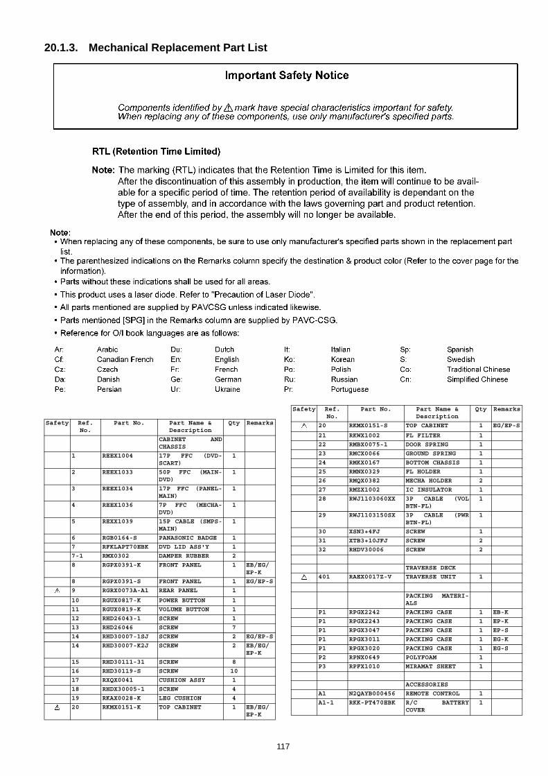
20.1.3. Mechanical Replacement Part List
Safety Ref. No.
Part No. Part Name & Description
Qty Remarks
CABINET ANDCHASSIS
1 REEX1004 17P FFC (DVD-SCART)
1
2 REEX1033 50P FFC (MAIN-DVD)
1
3 REEX1034 17P FFC (PANEL-MAIN)
1
4 REEX1036 7P FFC (MECHA-DVD)
1
5 REXX1039 15P CABLE (SMPS-MAIN)
1
6 RGB0164-S PANASONIC BADGE 1
7 RFKLAPT70EBK DVD LID ASS'Y 1
7-1 RMX0302 DAMPER RUBBER 2
8 RGPX0391-K FRONT PANEL 1 EB/EG/EP-K
8 RGPX0391-S FRONT PANEL 1 EG/EP-S
9 RGRX0073A-A1 REAR PANEL 1
10 RGUX0817-K POWER BUTTON 1
11 RGUX0819-K VOLUME BUTTON 1
12 RHD26043-1 SCREW 1
13 RHD26046 SCREW 7
14 RHD30007-1SJ SCREW 2 EG/EP-S
14 RHD30007-K2J SCREW 2 EB/EG/EP-K
15 RHD30111-31 SCREW 8
16 RHD30119-S SCREW 10
17 RXQX0041 CUSHION ASSY 1
18 RHDX30005-1 SCREW 4
19 RKAX0028-K LEG CUSHION 4
20 RKMX0151-K TOP CABINET 1 EB/EG/EP-K
20 RKMX0151-S TOP CABINET 1 EG/EP-S
21 RKWX1002 FL FILTER 1
22 RMBX0075-1 DOOR SPRING 1
23 RMCX0066 GROUND SPRING 1
24 RMKX0167 BOTTOM CHASSIS 1
25 RMNX0329 FL HOLDER 1
26 RMQX0382 MECHA HOLDER 2
27 RMZX1002 IC INSULATOR 1
28 RWJ1103060XX 3P CABLE (VOLBTN-FL)
1
29 RWJ1103150SX 3P CABLE (PWRBTN-FL)
1
30 XSN3+4FJ SCREW 1
31 XTB3+10JFJ SCREW 2
32 RHDV30006 SCREW 2
TRAVERSE DECK
401 RAEX0017Z-V TRAVERSE UNIT 1
PACKING MATERI-ALS
P1 RPGX2242 PACKING CASE 1 EB-K
P1 RPGX2243 PACKING CASE 1 EP-K
P1 RPGX3047 PACKING CASE 1 EP-S
P1 RPGX3011 PACKING CASE 1 EG-K
P1 RPGX3020 PACKING CASE 1 EG-S
P2 RPNX0649 POLYFOAM 1
P3 RPFX1010 MIRAMAT SHEET 1
ACCESSORIES
A1 N2QAYB000456 REMOTE CONTROL 1
A1-1 RKK-PT470EBK R/C BATTERYCOVER
1
Safety Ref. No.
Part No. Part Name & Description
Qty Remarks
117
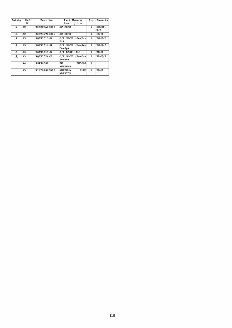
A2 K2CQ2CA00007 AC CORD 1 EG/EP-K/S
A2 K2CZ3YY00005 AC CORD 1 EB-K
A3 RQTX1013-D O/I BOOK (Ge/Fr/It)
1 EG-K/S
A3 RQTX1014-H O/I BOOK (Du/Sw/Da/Sp)
1 EG-K/S
A3 RQTX1019-B O/I BOOK (En) 1 EB-K
A3 RQTX1024-Z O/I BOOK (En/Cz/Po/Hu)
1 EP-K/S
A4 RSAX0002 FM INDOORANTENNA
1
A5 K1YZ02000013 ANTENNA PLUGADAPTOR
1 EB-K
Safety Ref. No.
Part No. Part Name & Description
Qty Remarks
118
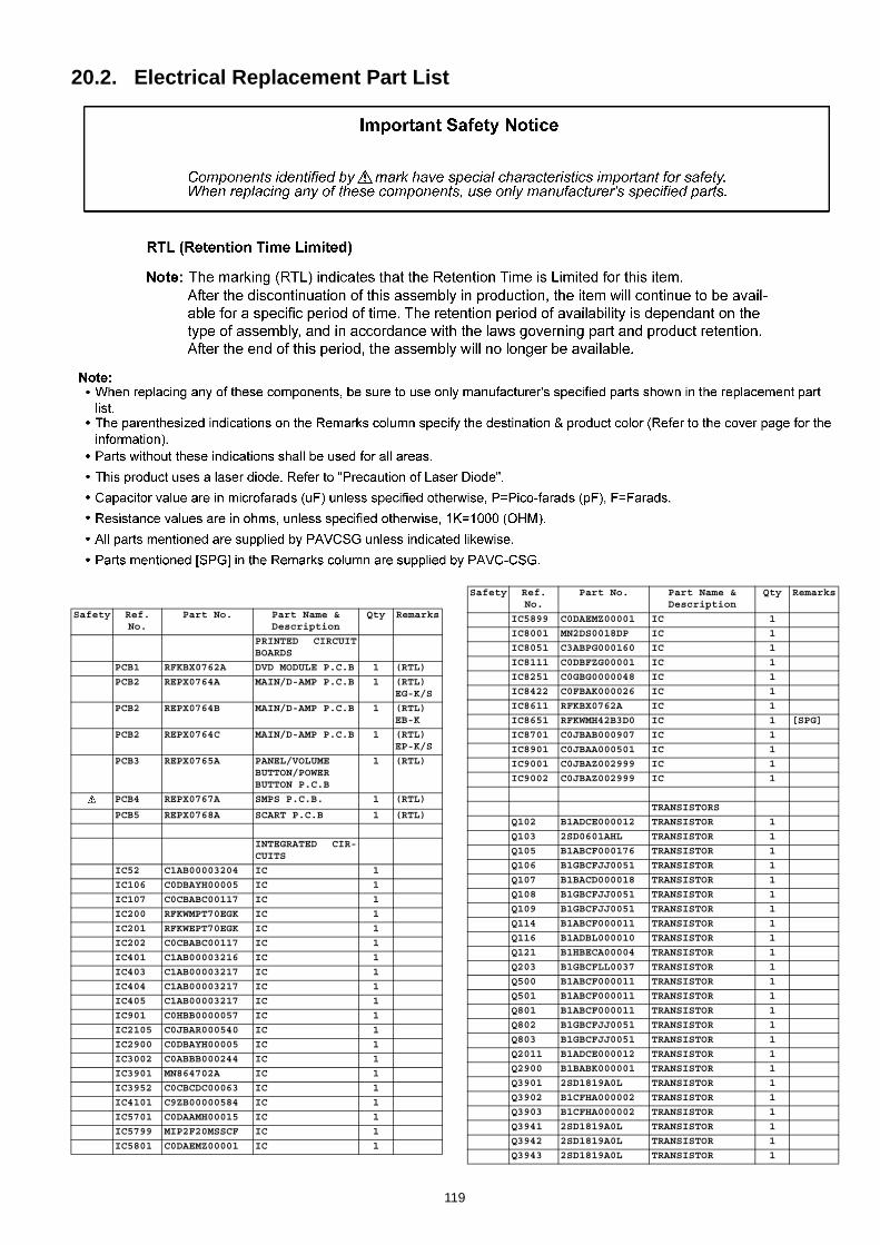
20.2. Electrical Replacement Part List
Safety Ref. No.
Part No. Part Name & Description
Qty Remarks
PRINTED CIRCUITBOARDS
PCB1 RFKBX0762A DVD MODULE P.C.B 1 (RTL)
PCB2 REPX0764A MAIN/D-AMP P.C.B 1 (RTL)EG-K/S
PCB2 REPX0764B MAIN/D-AMP P.C.B 1 (RTL)EB-K
PCB2 REPX0764C MAIN/D-AMP P.C.B 1 (RTL)EP-K/S
PCB3 REPX0765A PANEL/VOLUMEBUTTON/POWERBUTTON P.C.B
1 (RTL)
PCB4 REPX0767A SMPS P.C.B. 1 (RTL)
PCB5 REPX0768A SCART P.C.B 1 (RTL)
INTEGRATED CIR-CUITS
IC52 C1AB00003204 IC 1
IC106 C0DBAYH00005 IC 1
IC107 C0CBABC00117 IC 1
IC200 RFKWMPT70EGK IC 1
IC201 RFKWEPT70EGK IC 1
IC202 C0CBABC00117 IC 1
IC401 C1AB00003216 IC 1
IC403 C1AB00003217 IC 1
IC404 C1AB00003217 IC 1
IC405 C1AB00003217 IC 1
IC901 C0HBB0000057 IC 1
IC2105 C0JBAR000540 IC 1
IC2900 C0DBAYH00005 IC 1
IC3002 C0ABBB000244 IC 1
IC3901 MN864702A IC 1
IC3952 C0CBCDC00063 IC 1
IC4101 C9ZB00000584 IC 1
IC5701 C0DAAMH00015 IC 1
IC5799 MIP2F20MSSCF IC 1
IC5801 C0DAEMZ00001 IC 1
IC5899 C0DAEMZ00001 IC 1
IC8001 MN2DS0018DP IC 1
IC8051 C3ABPG000160 IC 1
IC8111 C0DBFZG00001 IC 1
IC8251 C0GBG0000048 IC 1
IC8422 C0FBAK000026 IC 1
IC8611 RFKBX0762A IC 1
IC8651 RFKWMH42B3D0 IC 1 [SPG]
IC8701 C0JBAB000907 IC 1
IC8901 C0JBAA000501 IC 1
IC9001 C0JBAZ002999 IC 1
IC9002 C0JBAZ002999 IC 1
TRANSISTORS
Q102 B1ADCE000012 TRANSISTOR 1
Q103 2SD0601AHL TRANSISTOR 1
Q105 B1ABCF000176 TRANSISTOR 1
Q106 B1GBCFJJ0051 TRANSISTOR 1
Q107 B1BACD000018 TRANSISTOR 1
Q108 B1GBCFJJ0051 TRANSISTOR 1
Q109 B1GBCFJJ0051 TRANSISTOR 1
Q114 B1ABCF000011 TRANSISTOR 1
Q116 B1ADBL000010 TRANSISTOR 1
Q121 B1HBECA00004 TRANSISTOR 1
Q203 B1GBCFLL0037 TRANSISTOR 1
Q500 B1ABCF000011 TRANSISTOR 1
Q501 B1ABCF000011 TRANSISTOR 1
Q801 B1ABCF000011 TRANSISTOR 1
Q802 B1GBCFJJ0051 TRANSISTOR 1
Q803 B1GBCFJJ0051 TRANSISTOR 1
Q2011 B1ADCE000012 TRANSISTOR 1
Q2900 B1BABK000001 TRANSISTOR 1
Q3901 2SD1819A0L TRANSISTOR 1
Q3902 B1CFHA000002 TRANSISTOR 1
Q3903 B1CFHA000002 TRANSISTOR 1
Q3941 2SD1819A0L TRANSISTOR 1
Q3942 2SD1819A0L TRANSISTOR 1
Q3943 2SD1819A0L TRANSISTOR 1
Safety Ref. No.
Part No. Part Name & Description
Qty Remarks
119
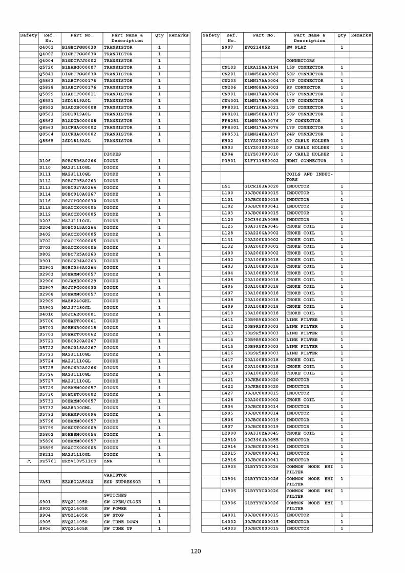
Q4001 B1GBCFGG0030 TRANSISTOR 1
Q4002 B1GBCFGG0030 TRANSISTOR 1
Q4004 B1GDCFJJ0002 TRANSISTOR 1
Q5720 B1BABG000007 TRANSISTOR 1
Q5841 B1GBCFGG0030 TRANSISTOR 1
Q5863 B1ABCF000176 TRANSISTOR 1
Q5898 B1ABCF000176 TRANSISTOR 1
Q5899 B1ABCF000011 TRANSISTOR 1
Q8551 2SD1819A0L TRANSISTOR 1
Q8552 B1ADGB000008 TRANSISTOR 1
Q8561 2SD1819A0L TRANSISTOR 1
Q8562 B1ADGB000008 TRANSISTOR 1
Q8563 B1CFHA000002 TRANSISTOR 1
Q8564 B1CFHA000002 TRANSISTOR 1
Q8565 2SD1819A0L TRANSISTOR 1
DIODES
D106 B0BC5R6A0266 DIODE 1
D110 MA2J1110GL DIODE 1
D111 MA2J1110GL DIODE 1
D112 B0BC7R5A0263 DIODE 1
D113 B0BC027A0264 DIODE 1
D114 B0BC010A0267 DIODE 1
D116 B0JCPG000030 DIODE 1
D118 B0ACCK000005 DIODE 1
D119 B0ACCK000005 DIODE 1
D203 MA2J1110GL DIODE 1
D204 B0BC015A0264 DIODE 1
D402 B0ACCK000005 DIODE 1
D702 B0ACCK000005 DIODE 1
D703 B0ACCK000005 DIODE 1
D802 B0BC7R5A0263 DIODE 1
D901 B0BC2R4A0263 DIODE 1
D2901 B0BC036A0264 DIODE 1
D2903 B0EAMM000057 DIODE 1
D2906 B0JAME000029 DIODE 1
D2907 B0JCPG000030 DIODE 1
D2908 B0EAMM000057 DIODE 1
D2909 MAZ8240GHL DIODE 1
D3901 MA2J7280GL DIODE 1
D4010 B0JCAE000001 DIODE 1
D5700 B0EAKT000061 DIODE 1
D5701 B0EBNR000015 DIODE 1
D5703 B0EAKT000062 DIODE 1
D5721 B0BC020A0267 DIODE 1
D5722 B0BC018A0267 DIODE 1
D5723 MA2J1110GL DIODE 1
D5724 MA2J1110GL DIODE 1
D5725 B0BC6R2A0266 DIODE 1
D5726 MA2J1110GL DIODE 1
D5727 MA2J1110GL DIODE 1
D5729 B0EAMM000057 DIODE 1
D5730 B0ECET000002 DIODE 1
D5731 B0EAMM000057 DIODE 1
D5732 MAZ8300GML DIODE 1
D5793 B0HAMP000094 DIODE 1
D5798 B0EAMM000057 DIODE 1
D5799 B0EDKT000009 DIODE 1
D5802 B0HBSM000054 DIODE 1
D5896 B0EAMM000057 DIODE 1
D5899 B0ACCK000005 DIODE 1
D8211 MA2J1110GL DIODE 1
DZ5701 ERZV10V511CS ZNR 1
VARISTOR
VA51 EZAEG2A50AX ESD SUPRESSOR 1
SWITCHES
S901 EVQ21405R SW OPEN/CLOSE 1
S902 EVQ21405R SW POWER 1
S904 EVQ21405R SW STOP 1
S905 EVQ21405R SW TUNE DOWN 1
S906 EVQ21405R SW TUNE UP 1
Safety Ref. No.
Part No. Part Name & Description
Qty Remarks
S907 EVQ21405R SW PLAY 1
CONNECTORS
CN103 K1KA15AA0194 15P CONNECTOR 1
CN201 K1MN50AA0082 50P CONNECTOR 1
CN203 K1MN17AA0004 17P CONNECTOR 1
CN206 K1MN08AA0003 8P CONNECTOR 1
CN901 K1MN17AA0004 17P CONNECTOR 1
CN4001 K1MN17BA0005 17P CONNECTOR 1
FP8031 K1MY10AA0021 10P CONNECTOR 1
FP8101 K1MN50BA0173 50P CONNECTOR 1
FP8251 K1MN07AA0076 7P CONNECTOR 1
FP8301 K1MN17AA0076 17P CONNECTOR 1
FP8531 K1MN24BA0197 24P CONNECTOR 1
H902 K1YZ03000010 3P CABLE HOLDER 1
H903 K1YZ03000010 3P CABLE HOLDER 1
H904 K1YZ03000010 3P CABLE HOLDER 1
P3901 K1FY119E0002 HDMI CONNECTOR 1
COILS AND INDUC-TORS
L51 G1CR18JA0020 INDUCTOR 1
L100 J0JBC0000015 INDUCTOR 1
L101 J0JBC0000015 INDUCTOR 1
L102 J0JBC0000041 INDUCTOR 1
L103 J0JBC0000015 INDUCTOR 1
L120 G0C390JA0055 INDUCTOR 1
L125 G0A330ZA0045 CHOKE COIL 1
L128 G0A220GA0002 CHOKE COIL 1
L131 G0A200D00002 CHOKE COIL 1
L132 G0A200D00002 CHOKE COIL 1
L400 G0A200D00002 CHOKE COIL 1
L402 G0A100H00018 CHOKE COIL 1
L403 G0A100H00018 CHOKE COIL 1
L404 G0A100H00018 CHOKE COIL 1
L405 G0A100H00018 CHOKE COIL 1
L406 G0A100H00018 CHOKE COIL 1
L407 G0A100H00018 CHOKE COIL 1
L408 G0A100H00018 CHOKE COIL 1
L409 G0A100H00018 CHOKE COIL 1
L410 G0A100H00018 CHOKE COIL 1
L411 G0B9R5K00003 LINE FILTER 1
L412 G0B9R5K00003 LINE FILTER 1
L413 G0B9R5K00003 LINE FILTER 1
L414 G0B9R5K00003 LINE FILTER 1
L415 G0B9R5K00003 LINE FILTER 1
L416 G0B9R5K00003 LINE FILTER 1
L417 G0A100H00018 CHOKE COIL 1
L418 G0A100H00018 CHOKE COIL 1
L419 G0A100H00018 CHOKE COIL 1
L421 J0JKB0000020 INDUCTOR 1
L422 J0JKB0000020 INDUCTOR 1
L427 J0JBC0000015 INDUCTOR 1
L428 G0A200D00002 CHOKE COIL 1
L904 J0JBC0000014 INDUCTOR 1
L905 J0JBC0000014 INDUCTOR 1
L906 J0JBC0000019 INDUCTOR 1
L907 J0JBC0000019 INDUCTOR 1
L2900 G0A330ZA0045 CHOKE COIL 1
L2910 G0C390JA0055 INDUCTOR 1
L2914 J0JBC0000041 INDUCTOR 1
L2915 J0JBC0000041 INDUCTOR 1
L2916 J0JBC0000041 INDUCTOR 1
L3903 G1BYYYC00026 COMMON MODE EMIFILTER
1
L3904 G1BYYYC00026 COMMON MODE EMIFILTER
1
L3905 G1BYYYC00026 COMMON MODE EMIFILTER
1
L3906 G1BYYYC00026 COMMON MODE EMIFILTER
1
L4001 J0JBC0000015 INDUCTOR 1
L4002 J0JBC0000015 INDUCTOR 1
L4003 J0JBC0000015 INDUCTOR 1
Safety Ref. No.
Part No. Part Name & Description
Qty Remarks
120
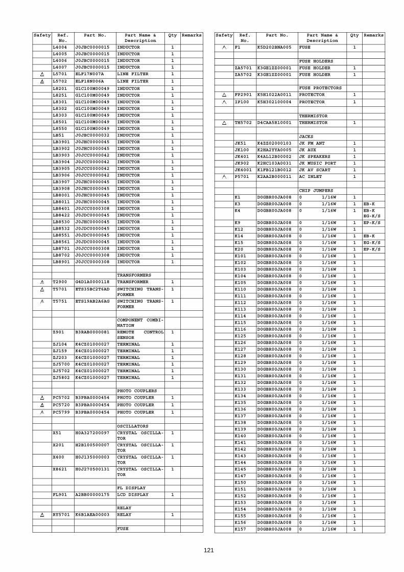
L4004 J0JBC0000015 INDUCTOR 1
L4005 J0JBC0000015 INDUCTOR 1
L4006 J0JBC0000015 INDUCTOR 1
L4007 J0JBC0000015 INDUCTOR 1
L5701 ELF17N007A LINE FILTER 1
L5702 ELF18N006A LINE FILTER 1
L8201 G1C100M00049 INDUCTOR 1
L8251 G1C100M00049 INDUCTOR 1
L8301 G1C100M00049 INDUCTOR 1
L8302 G1C100M00049 INDUCTOR 1
L8303 G1C100M00049 INDUCTOR 1
L8501 G1C100M00049 INDUCTOR 1
L8550 G1C100M00049 INDUCTOR 1
LB51 J0JBC0000032 INDUCTOR 1
LB3901 J0JHC0000045 INDUCTOR 1
LB3902 J0JHC0000045 INDUCTOR 1
LB3903 J0JCC0000042 INDUCTOR 1
LB3904 J0JCC0000042 INDUCTOR 1
LB3905 J0JCC0000042 INDUCTOR 1
LB3906 J0JCC0000042 INDUCTOR 1
LB3907 J0JHC0000045 INDUCTOR 1
LB3908 J0JHC0000045 INDUCTOR 1
LB8001 J0JHC0000045 INDUCTOR 1
LB8011 J0JHC0000045 INDUCTOR 1
LB8401 J0JCC0000308 INDUCTOR 1
LB8422 J0JDC0000045 INDUCTOR 1
LB8530 J0JHC0000045 INDUCTOR 1
LB8532 J0JDC0000045 INDUCTOR 1
LB8551 J0JDC0000045 INDUCTOR 1
LB8561 J0JDC0000045 INDUCTOR 1
LB8701 J0JCC0000308 INDUCTOR 1
LB8702 J0JCC0000308 INDUCTOR 1
LB8901 J0JCC0000308 INDUCTOR 1
TRANSFORMERS
T2900 G4D1A0000118 TRANSFORMER 1
T5701 ETS35BC2T6AD SWITCHING TRANS-FORMER
1
T5751 ETS19AB2A6AG SWITCHING TRANS-FORMER
1
COMPONENT COMBI-NATION
Z901 B3RAB0000081 REMOTE CONTROLSENSOR
1
ZJ104 K4CZ01000027 TERMINAL 1
ZJ159 K4CZ01000027 TERMINAL 1
ZJ203 K4CZ01000027 TERMINAL 1
ZJ5700 K4CZ01000027 TERMINAL 1
ZJ5702 K4CZ01000027 TERMINAL 1
ZJ5802 K4CZ01000027 TERMINAL 1
PHOTO COUPLERS
PC5702 B3PBA0000454 PHOTO COUPLER 1
PC5720 B3PBA0000454 PHOTO COUPLER 1
PC5799 B3PBA0000454 PHOTO COUPLER 1
OSCILLATORS
X51 H0A327200097 CRYSTAL OSCILLA-TOR
1
X201 H2B100500007 CRYSTAL OSCILLA-TOR
1
X400 H0J135000003 CRYSTAL OSCILLA-TOR
1
X8621 H0J270500131 CRYSTAL OSCILLA-TOR
1
FL DISPLAY
FL901 A2BB00000175 LCD DISPLAY 1
RELAY
RY5701 K6B1AEA00003 RELAY 1
FUSE
Safety Ref. No.
Part No. Part Name & Description
Qty Remarks
F1 K5D202BNA005 FUSE 1
FUSE HOLDERS
ZA5701 K3GE1ZZ00001 FUSE HOLDER 1
ZA5702 K3GE1ZZ00001 FUSE HOLDER 1
FUSE PROTECTORS
FP2901 K5H1022A0011 PROTECTOR 1
IP100 K5H302100004 PROTECTOR 1
THERMISTOR
TH5702 D4CAA5R10001 THERMISTOR 1
JACKS
JK51 K4ZZ02000103 JK FM ANT 1
JK100 K2HA2YYA0005 JK AUX 1
JK401 K4AL12B00002 JK SPEAKERS 1
JK902 K2HC103A0031 JK MUSIC PORT 1
JK4001 K1FB121B0012 JK AV SCART 1
P5701 K2AA2B000011 AC INLET 1
CHIP JUMPERS
K1 D0GBR00JA008 0 1/16W 1
K3 D0GBR00JA008 0 1/16W 1 EB-K
K4 D0GBR00JA008 0 1/16W 1 EB-KEG-K/S
K9 D0GBR00JA008 0 1/16W 1 EP-K/S
K12 D0GBR00JA008 0 1/16W 1
K14 D0GBR00JA008 0 1/16W 1 EB-K
K15 D0GBR00JA008 0 1/16W 1 EG-K/S
K20 D0GBR00JA008 0 1/16W 1 EP-K/S
K101 D0GBR00JA008 0 1/16W 1
K102 D0GBR00JA008 0 1/16W 1
K103 D0GBR00JA008 0 1/16W 1
K104 D0GBR00JA008 0 1/16W 1
K105 D0GBR00JA008 0 1/16W 1
K110 D0GBR00JA008 0 1/16W 1
K111 D0GBR00JA008 0 1/16W 1
K112 D0GBR00JA008 0 1/16W 1
K113 D0GBR00JA008 0 1/16W 1
K114 D0GBR00JA008 0 1/16W 1
K115 D0GBR00JA008 0 1/16W 1
K116 D0GBR00JA008 0 1/16W 1
K125 D0GBR00JA008 0 1/16W 1
K126 D0GBR00JA008 0 1/16W 1
K127 D0GBR00JA008 0 1/16W 1
K128 D0GBR00JA008 0 1/16W 1
K129 D0GBR00JA008 0 1/16W 1
K130 D0GBR00JA008 0 1/16W 1
K131 D0GBR00JA008 0 1/16W 1
K132 D0GBR00JA008 0 1/16W 1
K133 D0GBR00JA008 0 1/16W 1
K134 D0GBR00JA008 0 1/16W 1
K135 D0GBR00JA008 0 1/16W 1
K136 D0GBR00JA008 0 1/16W 1
K137 D0GBR00JA008 0 1/16W 1
K138 D0GBR00JA008 0 1/16W 1
K139 D0GBR00JA008 0 1/16W 1
K140 D0GBR00JA008 0 1/16W 1
K141 D0GBR00JA008 0 1/16W 1
K142 D0GBR00JA008 0 1/16W 1
K143 D0GBR00JA008 0 1/16W 1
K144 D0GBR00JA008 0 1/16W 1
K145 D0GBR00JA008 0 1/16W 1
K147 D0GBR00JA008 0 1/16W 1
K150 D0GBR00JA008 0 1/16W 1
K151 D0GBR00JA008 0 1/16W 1
K152 D0GBR00JA008 0 1/16W 1
K153 D0GBR00JA008 0 1/16W 1
K154 D0GBR00JA008 0 1/16W 1
K155 D0GBR00JA008 0 1/16W 1
K156 D0GBR00JA008 0 1/16W 1
K157 D0GBR00JA008 0 1/16W 1
Safety Ref. No.
Part No. Part Name & Description
Qty Remarks
121
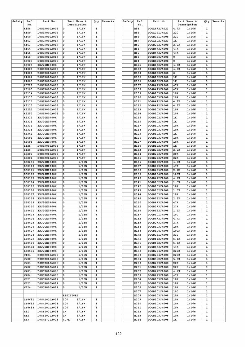
K158 D0GBR00JA008 0 1/16W 1
K159 D0GBR00JA008 0 1/16W 1
K160 D0GBR00JA008 0 1/16W 1
K162 D0GDR00JA017 0 1/10W 1
K163 D0GDR00JA017 0 1/10W 1
K164 D0GDR00JA017 0 1/10W 1
K165 D0GDR00JA017 0 1/10W 1
K166 D0GDR00JA017 0 1/10W 1
K3903 D0GBR00JA008 0 1/16W 1
K3905 ERJ2GE0R00X 0 1/16W 1
K4000 D0GBR00JA008 0 1/16W 1
K4001 D0GBR00JA008 0 1/16W 1
K4002 D0GBR00JA008 0 1/16W 1
K4003 D0GBR00JA008 0 1/16W 1
K5721 D0GBR00JA008 0 1/16W 1
K8100 D0GBR00JA008 0 1/16W 1
K8114 D0GBR00JA008 0 1/16W 1
K8115 D0GBR00JA008 0 1/16W 1
K8116 D0GBR00JA008 0 1/16W 1
K8117 D0GBR00JA008 0 1/16W 1
K8251 D0GBR00JA008 0 1/16W 1
K8252 D0GBR00JA008 0 1/16W 1
K8321 ERJ2GE0R00X 0 1/16W 1
K8325 ERJ2GE0R00X 0 1/16W 1
K8331 ERJ2GE0R00X 0 1/16W 1
K8335 ERJ2GE0R00X 0 1/16W 1
K8341 ERJ2GE0R00X 0 1/16W 1
K8691 ERJ2GE0R00X 0 1/16W 1
K8695 ERJ2GE0R00X 0 1/16W 1
L425 D0GBR00JA008 0 1/16W 1
L426 D0GBR00JA008 0 1/16W 1
LB200 D0GBR00JA008 0 1/16W 1
LB201 D0GBR00JA008 0 1/16W 1
LB8255 ERJ2GE0R00X 0 1/16W 1
LB8310 ERJ2GE0R00X 0 1/16W 1
LB8311 ERJ2GE0R00X 0 1/16W 1
LB8312 ERJ2GE0R00X 0 1/16W 1
LB8313 ERJ2GE0R00X 0 1/16W 1
LB8314 ERJ2GE0R00X 0 1/16W 1
LB8315 ERJ2GE0R00X 0 1/16W 1
LB8316 ERJ2GE0R00X 0 1/16W 1
LB8317 ERJ2GE0R00X 0 1/16W 1
LB8318 ERJ2GE0R00X 0 1/16W 1
LB8319 ERJ2GE0R00X 0 1/16W 1
LB8320 ERJ2GE0R00X 0 1/16W 1
LB8421 ERJ2GE0R00X 0 1/16W 1
LB8423 ERJ2GE0R00X 0 1/16W 1
LB8424 ERJ2GE0R00X 0 1/16W 1
LB8425 ERJ2GE0R00X 0 1/16W 1
LB8426 ERJ2GE0R00X 0 1/16W 1
LB8427 ERJ2GE0R00X 0 1/16W 1
LB8428 ERJ2GE0R00X 0 1/16W 1
LB8429 ERJ2GE0R00X 0 1/16W 1
LB8430 ERJ2GE0R00X 0 1/16W 1
LB8432 ERJ2GE0R00X 0 1/16W 1
LB8531 ERJ2GE0R00X 0 1/16W 1
W101 D0GBR00JA008 0 1/16W 1
W780 D0GBR00JA008 0 1/16W 1
W781 D0GBR00JA008 0 1/16W 1
W782 D0GDR00JA017 0 1/10W 1
W783 D0GBR00JA008 0 1/16W 1
W784 D0GBR00JA008 0 1/16W 1
W921 D0GDR00JA017 0 1/10W 1
W923 D0GDR00JA017 0 1/10W 1
W924 D0GDR00JA017 0 1/10W 1
RESISTORS
LB8691 D0GA101JA023 100 1/16W 1
LB8692 D0GA101JA023 100 1/16W 1
LB8693 D0GA101JA023 100 1/16W 1
R51 D0GB102JA008 1K 1/16W 1
R52 D0GB102JA008 1K 1/16W 1
R53 D0GA472JA023 4.7K 1/16W 1
Safety Ref. No.
Part No. Part Name & Description
Qty Remarks
R54 D0GA472JA023 4.7K 1/16W 1
R55 D0GA221JA023 220 1/16W 1
R56 D0GB221JA008 220 1/16W 1
R57 D0GA102JA023 1K 1/16W 1
R59 D0GB222JA008 2.2K 1/16W 1
R61 D0GB473JA008 47K 1/16W 1
R62 D0GB473JA008 47K 1/16W 1
R63 D0GBR00JA008 0 1/16W 1
R64 D0GBR00JA008 0 1/16W 1
R101 D0GB472JA008 4.7K 1/16W 1
R102 D0GB472JA008 4.7K 1/16W 1
R103 D0GBR00JA008 0 1/16W 1
R105 D0GB102JA008 1K 1/16W 1
R106 D0GB102JA008 1K 1/16W 1
R107 D0GB473JA008 47K 1/16W 1
R108 D0GB473JA008 47K 1/16W 1
R109 D0GB103JA008 10K 1/16W 1
R110 D0GB103JA008 10K 1/16W 1
R111 D0GB472JA008 4.7K 1/16W 1
R112 D0GB472JA008 4.7K 1/16W 1
R113 D0GB103JA008 10K 1/16W 1
R114 D0GB103JA008 10K 1/16W 1
R115 D0GB102JA008 1K 1/16W 1
R116 D0GB102JA008 1K 1/16W 1
R117 D0GB103JA008 10K 1/16W 1
R118 D0GB103JA008 10K 1/16W 1
R125 D0GB102JA008 1K 1/16W 1
R126 D0GB103JA008 10K 1/16W 1
R127 D0GB103JA008 10K 1/16W 1
R130 D0GB102JA008 1K 1/16W 1
R133 D0GB222JA008 2.2K 1/16W 1
R134 D0GB203JA008 20K 1/16W 1
R135 D0GB223JA008 22K 1/16W 1
R136 D0GB472JA008 4.7K 1/16W 1
R137 D0GB473JA008 47K 1/16W 1
R138 D0GB225JA008 2.2M 1/16W 1
R139 D0GB104JA008 100K 1/16W 1
R140 D0GB472JA008 4.7K 1/16W 1
R141 D0GB152JA008 1.5K 1/16W 1
R142 D0GB103JA008 10K 1/16W 1
R143 D0GB152JA008 1.5K 1/16W 1
R144 D0GB103JA008 10K 1/16W 1
R146 D0GB222JA008 2.2K 1/16W 1
R150 D0GB473JA008 47K 1/16W 1
R152 D0GB273JA008 27K 1/16W 1
R156 D0GB122JA008 1.2K 1/16W 1
R157 D0GB101JA008 100 1/16W 1
R162 D0GB472JA008 4.7K 1/16W 1
R163 D0GB273JA008 27K 1/16W 1
R164 D0GB103JA008 10K 1/16W 1
R168 D0GB104JA008 100K 1/16W 1
R172 D0GB221JA008 220 1/16W 1
R175 D0GB562JA008 5.6K 1/16W 1
R176 D0GB562JA008 5.6K 1/16W 1
R178 D0GB473JA008 47K 1/16W 1
R179 D0GB224JA008 220K 1/16W 1
R180 D0GB224JA008 220K 1/16W 1
R184 D0GB562JA008 5.6K 1/16W 1
R200 D0GB223JA008 22K 1/16W 1
R201 D0GB223JA008 22K 1/16W 1
R202 D0GB472JA008 4.7K 1/16W 1
R203 D0GB473JA008 47K 1/16W 1
R204 D0GB103JA008 10K 1/16W 1
R205 D0GB103JA008 10K 1/16W 1
R206 D0GB103JA008 10K 1/16W 1
R207 D0GB101JA008 100 1/16W 1
R208 D0GB103JA008 10K 1/16W 1
R209 D0GB103JA008 10K 1/16W 1
R210 D0GB103JA008 10K 1/16W 1
R211 D0GB103JA008 10K 1/16W 1
R212 D0GB103JA008 10K 1/16W 1
R213 D0GB103JA008 10K 1/16W 1
R214 D0GB102JA008 1K 1/16W 1
Safety Ref. No.
Part No. Part Name & Description
Qty Remarks
122
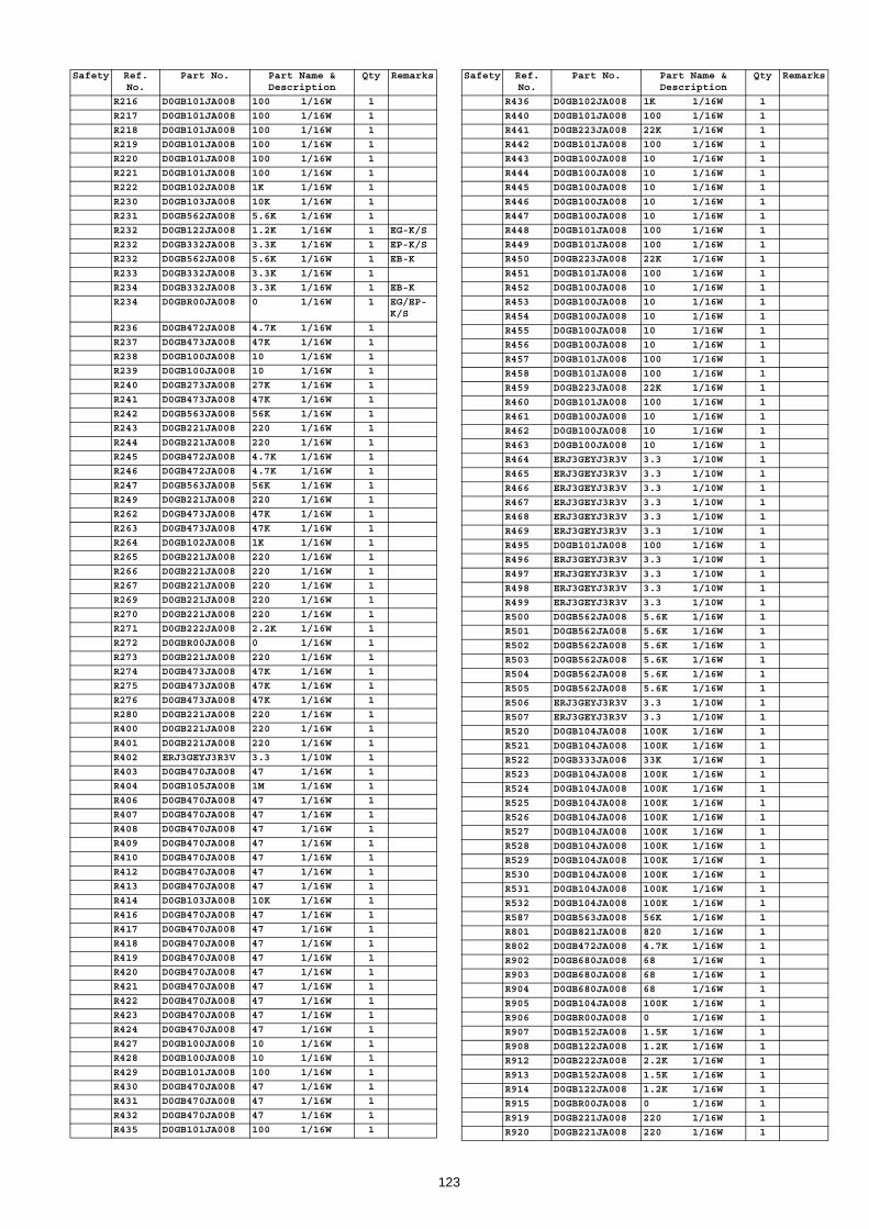
R216 D0GB101JA008 100 1/16W 1
R217 D0GB101JA008 100 1/16W 1
R218 D0GB101JA008 100 1/16W 1
R219 D0GB101JA008 100 1/16W 1
R220 D0GB101JA008 100 1/16W 1
R221 D0GB101JA008 100 1/16W 1
R222 D0GB102JA008 1K 1/16W 1
R230 D0GB103JA008 10K 1/16W 1
R231 D0GB562JA008 5.6K 1/16W 1
R232 D0GB122JA008 1.2K 1/16W 1 EG-K/S
R232 D0GB332JA008 3.3K 1/16W 1 EP-K/S
R232 D0GB562JA008 5.6K 1/16W 1 EB-K
R233 D0GB332JA008 3.3K 1/16W 1
R234 D0GB332JA008 3.3K 1/16W 1 EB-K
R234 D0GBR00JA008 0 1/16W 1 EG/EP-K/S
R236 D0GB472JA008 4.7K 1/16W 1
R237 D0GB473JA008 47K 1/16W 1
R238 D0GB100JA008 10 1/16W 1
R239 D0GB100JA008 10 1/16W 1
R240 D0GB273JA008 27K 1/16W 1
R241 D0GB473JA008 47K 1/16W 1
R242 D0GB563JA008 56K 1/16W 1
R243 D0GB221JA008 220 1/16W 1
R244 D0GB221JA008 220 1/16W 1
R245 D0GB472JA008 4.7K 1/16W 1
R246 D0GB472JA008 4.7K 1/16W 1
R247 D0GB563JA008 56K 1/16W 1
R249 D0GB221JA008 220 1/16W 1
R262 D0GB473JA008 47K 1/16W 1
R263 D0GB473JA008 47K 1/16W 1
R264 D0GB102JA008 1K 1/16W 1
R265 D0GB221JA008 220 1/16W 1
R266 D0GB221JA008 220 1/16W 1
R267 D0GB221JA008 220 1/16W 1
R269 D0GB221JA008 220 1/16W 1
R270 D0GB221JA008 220 1/16W 1
R271 D0GB222JA008 2.2K 1/16W 1
R272 D0GBR00JA008 0 1/16W 1
R273 D0GB221JA008 220 1/16W 1
R274 D0GB473JA008 47K 1/16W 1
R275 D0GB473JA008 47K 1/16W 1
R276 D0GB473JA008 47K 1/16W 1
R280 D0GB221JA008 220 1/16W 1
R400 D0GB221JA008 220 1/16W 1
R401 D0GB221JA008 220 1/16W 1
R402 ERJ3GEYJ3R3V 3.3 1/10W 1
R403 D0GB470JA008 47 1/16W 1
R404 D0GB105JA008 1M 1/16W 1
R406 D0GB470JA008 47 1/16W 1
R407 D0GB470JA008 47 1/16W 1
R408 D0GB470JA008 47 1/16W 1
R409 D0GB470JA008 47 1/16W 1
R410 D0GB470JA008 47 1/16W 1
R412 D0GB470JA008 47 1/16W 1
R413 D0GB470JA008 47 1/16W 1
R414 D0GB103JA008 10K 1/16W 1
R416 D0GB470JA008 47 1/16W 1
R417 D0GB470JA008 47 1/16W 1
R418 D0GB470JA008 47 1/16W 1
R419 D0GB470JA008 47 1/16W 1
R420 D0GB470JA008 47 1/16W 1
R421 D0GB470JA008 47 1/16W 1
R422 D0GB470JA008 47 1/16W 1
R423 D0GB470JA008 47 1/16W 1
R424 D0GB470JA008 47 1/16W 1
R427 D0GB100JA008 10 1/16W 1
R428 D0GB100JA008 10 1/16W 1
R429 D0GB101JA008 100 1/16W 1
R430 D0GB470JA008 47 1/16W 1
R431 D0GB470JA008 47 1/16W 1
R432 D0GB470JA008 47 1/16W 1
R435 D0GB101JA008 100 1/16W 1
Safety Ref. No.
Part No. Part Name & Description
Qty Remarks
R436 D0GB102JA008 1K 1/16W 1
R440 D0GB101JA008 100 1/16W 1
R441 D0GB223JA008 22K 1/16W 1
R442 D0GB101JA008 100 1/16W 1
R443 D0GB100JA008 10 1/16W 1
R444 D0GB100JA008 10 1/16W 1
R445 D0GB100JA008 10 1/16W 1
R446 D0GB100JA008 10 1/16W 1
R447 D0GB100JA008 10 1/16W 1
R448 D0GB101JA008 100 1/16W 1
R449 D0GB101JA008 100 1/16W 1
R450 D0GB223JA008 22K 1/16W 1
R451 D0GB101JA008 100 1/16W 1
R452 D0GB100JA008 10 1/16W 1
R453 D0GB100JA008 10 1/16W 1
R454 D0GB100JA008 10 1/16W 1
R455 D0GB100JA008 10 1/16W 1
R456 D0GB100JA008 10 1/16W 1
R457 D0GB101JA008 100 1/16W 1
R458 D0GB101JA008 100 1/16W 1
R459 D0GB223JA008 22K 1/16W 1
R460 D0GB101JA008 100 1/16W 1
R461 D0GB100JA008 10 1/16W 1
R462 D0GB100JA008 10 1/16W 1
R463 D0GB100JA008 10 1/16W 1
R464 ERJ3GEYJ3R3V 3.3 1/10W 1
R465 ERJ3GEYJ3R3V 3.3 1/10W 1
R466 ERJ3GEYJ3R3V 3.3 1/10W 1
R467 ERJ3GEYJ3R3V 3.3 1/10W 1
R468 ERJ3GEYJ3R3V 3.3 1/10W 1
R469 ERJ3GEYJ3R3V 3.3 1/10W 1
R495 D0GB101JA008 100 1/16W 1
R496 ERJ3GEYJ3R3V 3.3 1/10W 1
R497 ERJ3GEYJ3R3V 3.3 1/10W 1
R498 ERJ3GEYJ3R3V 3.3 1/10W 1
R499 ERJ3GEYJ3R3V 3.3 1/10W 1
R500 D0GB562JA008 5.6K 1/16W 1
R501 D0GB562JA008 5.6K 1/16W 1
R502 D0GB562JA008 5.6K 1/16W 1
R503 D0GB562JA008 5.6K 1/16W 1
R504 D0GB562JA008 5.6K 1/16W 1
R505 D0GB562JA008 5.6K 1/16W 1
R506 ERJ3GEYJ3R3V 3.3 1/10W 1
R507 ERJ3GEYJ3R3V 3.3 1/10W 1
R520 D0GB104JA008 100K 1/16W 1
R521 D0GB104JA008 100K 1/16W 1
R522 D0GB333JA008 33K 1/16W 1
R523 D0GB104JA008 100K 1/16W 1
R524 D0GB104JA008 100K 1/16W 1
R525 D0GB104JA008 100K 1/16W 1
R526 D0GB104JA008 100K 1/16W 1
R527 D0GB104JA008 100K 1/16W 1
R528 D0GB104JA008 100K 1/16W 1
R529 D0GB104JA008 100K 1/16W 1
R530 D0GB104JA008 100K 1/16W 1
R531 D0GB104JA008 100K 1/16W 1
R532 D0GB104JA008 100K 1/16W 1
R587 D0GB563JA008 56K 1/16W 1
R801 D0GB821JA008 820 1/16W 1
R802 D0GB472JA008 4.7K 1/16W 1
R902 D0GB680JA008 68 1/16W 1
R903 D0GB680JA008 68 1/16W 1
R904 D0GB680JA008 68 1/16W 1
R905 D0GB104JA008 100K 1/16W 1
R906 D0GBR00JA008 0 1/16W 1
R907 D0GB152JA008 1.5K 1/16W 1
R908 D0GB122JA008 1.2K 1/16W 1
R912 D0GB222JA008 2.2K 1/16W 1
R913 D0GB152JA008 1.5K 1/16W 1
R914 D0GB122JA008 1.2K 1/16W 1
R915 D0GBR00JA008 0 1/16W 1
R919 D0GB221JA008 220 1/16W 1
R920 D0GB221JA008 220 1/16W 1
Safety Ref. No.
Part No. Part Name & Description
Qty Remarks
123
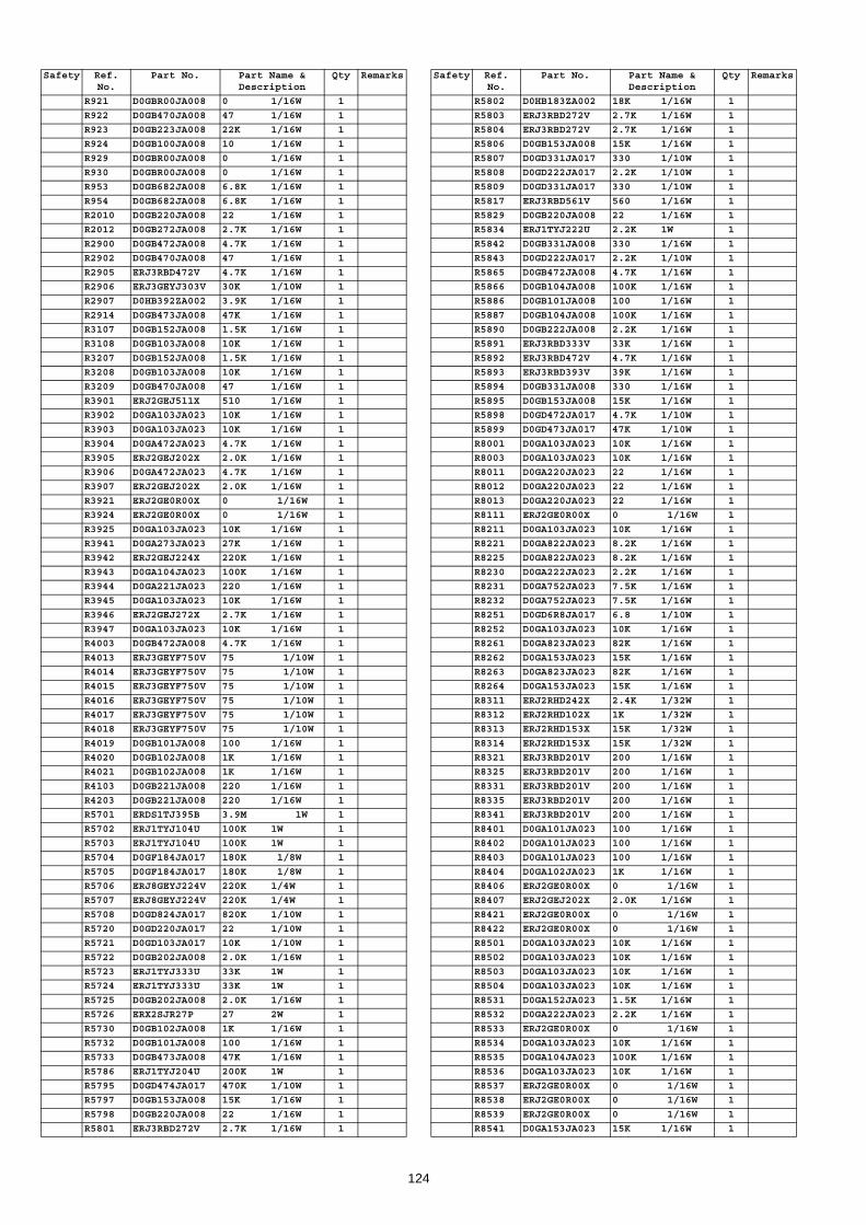
R921 D0GBR00JA008 0 1/16W 1
R922 D0GB470JA008 47 1/16W 1
R923 D0GB223JA008 22K 1/16W 1
R924 D0GB100JA008 10 1/16W 1
R929 D0GBR00JA008 0 1/16W 1
R930 D0GBR00JA008 0 1/16W 1
R953 D0GB682JA008 6.8K 1/16W 1
R954 D0GB682JA008 6.8K 1/16W 1
R2010 D0GB220JA008 22 1/16W 1
R2012 D0GB272JA008 2.7K 1/16W 1
R2900 D0GB472JA008 4.7K 1/16W 1
R2902 D0GB470JA008 47 1/16W 1
R2905 ERJ3RBD472V 4.7K 1/16W 1
R2906 ERJ3GEYJ303V 30K 1/10W 1
R2907 D0HB392ZA002 3.9K 1/16W 1
R2914 D0GB473JA008 47K 1/16W 1
R3107 D0GB152JA008 1.5K 1/16W 1
R3108 D0GB103JA008 10K 1/16W 1
R3207 D0GB152JA008 1.5K 1/16W 1
R3208 D0GB103JA008 10K 1/16W 1
R3209 D0GB470JA008 47 1/16W 1
R3901 ERJ2GEJ511X 510 1/16W 1
R3902 D0GA103JA023 10K 1/16W 1
R3903 D0GA103JA023 10K 1/16W 1
R3904 D0GA472JA023 4.7K 1/16W 1
R3905 ERJ2GEJ202X 2.0K 1/16W 1
R3906 D0GA472JA023 4.7K 1/16W 1
R3907 ERJ2GEJ202X 2.0K 1/16W 1
R3921 ERJ2GE0R00X 0 1/16W 1
R3924 ERJ2GE0R00X 0 1/16W 1
R3925 D0GA103JA023 10K 1/16W 1
R3941 D0GA273JA023 27K 1/16W 1
R3942 ERJ2GEJ224X 220K 1/16W 1
R3943 D0GA104JA023 100K 1/16W 1
R3944 D0GA221JA023 220 1/16W 1
R3945 D0GA103JA023 10K 1/16W 1
R3946 ERJ2GEJ272X 2.7K 1/16W 1
R3947 D0GA103JA023 10K 1/16W 1
R4003 D0GB472JA008 4.7K 1/16W 1
R4013 ERJ3GEYF750V 75 1/10W 1
R4014 ERJ3GEYF750V 75 1/10W 1
R4015 ERJ3GEYF750V 75 1/10W 1
R4016 ERJ3GEYF750V 75 1/10W 1
R4017 ERJ3GEYF750V 75 1/10W 1
R4018 ERJ3GEYF750V 75 1/10W 1
R4019 D0GB101JA008 100 1/16W 1
R4020 D0GB102JA008 1K 1/16W 1
R4021 D0GB102JA008 1K 1/16W 1
R4103 D0GB221JA008 220 1/16W 1
R4203 D0GB221JA008 220 1/16W 1
R5701 ERDS1TJ395B 3.9M 1W 1
R5702 ERJ1TYJ104U 100K 1W 1
R5703 ERJ1TYJ104U 100K 1W 1
R5704 D0GF184JA017 180K 1/8W 1
R5705 D0GF184JA017 180K 1/8W 1
R5706 ERJ8GEYJ224V 220K 1/4W 1
R5707 ERJ8GEYJ224V 220K 1/4W 1
R5708 D0GD824JA017 820K 1/10W 1
R5720 D0GD220JA017 22 1/10W 1
R5721 D0GD103JA017 10K 1/10W 1
R5722 D0GB202JA008 2.0K 1/16W 1
R5723 ERJ1TYJ333U 33K 1W 1
R5724 ERJ1TYJ333U 33K 1W 1
R5725 D0GB202JA008 2.0K 1/16W 1
R5726 ERX2SJR27P 27 2W 1
R5730 D0GB102JA008 1K 1/16W 1
R5732 D0GB101JA008 100 1/16W 1
R5733 D0GB473JA008 47K 1/16W 1
R5786 ERJ1TYJ204U 200K 1W 1
R5795 D0GD474JA017 470K 1/10W 1
R5797 D0GB153JA008 15K 1/16W 1
R5798 D0GB220JA008 22 1/16W 1
R5801 ERJ3RBD272V 2.7K 1/16W 1
Safety Ref. No.
Part No. Part Name & Description
Qty Remarks
R5802 D0HB183ZA002 18K 1/16W 1
R5803 ERJ3RBD272V 2.7K 1/16W 1
R5804 ERJ3RBD272V 2.7K 1/16W 1
R5806 D0GB153JA008 15K 1/16W 1
R5807 D0GD331JA017 330 1/10W 1
R5808 D0GD222JA017 2.2K 1/10W 1
R5809 D0GD331JA017 330 1/10W 1
R5817 ERJ3RBD561V 560 1/16W 1
R5829 D0GB220JA008 22 1/16W 1
R5834 ERJ1TYJ222U 2.2K 1W 1
R5842 D0GB331JA008 330 1/16W 1
R5843 D0GD222JA017 2.2K 1/10W 1
R5865 D0GB472JA008 4.7K 1/16W 1
R5866 D0GB104JA008 100K 1/16W 1
R5886 D0GB101JA008 100 1/16W 1
R5887 D0GB104JA008 100K 1/16W 1
R5890 D0GB222JA008 2.2K 1/16W 1
R5891 ERJ3RBD333V 33K 1/16W 1
R5892 ERJ3RBD472V 4.7K 1/16W 1
R5893 ERJ3RBD393V 39K 1/16W 1
R5894 D0GB331JA008 330 1/16W 1
R5895 D0GB153JA008 15K 1/16W 1
R5898 D0GD472JA017 4.7K 1/10W 1
R5899 D0GD473JA017 47K 1/10W 1
R8001 D0GA103JA023 10K 1/16W 1
R8003 D0GA103JA023 10K 1/16W 1
R8011 D0GA220JA023 22 1/16W 1
R8012 D0GA220JA023 22 1/16W 1
R8013 D0GA220JA023 22 1/16W 1
R8111 ERJ2GE0R00X 0 1/16W 1
R8211 D0GA103JA023 10K 1/16W 1
R8221 D0GA822JA023 8.2K 1/16W 1
R8225 D0GA822JA023 8.2K 1/16W 1
R8230 D0GA222JA023 2.2K 1/16W 1
R8231 D0GA752JA023 7.5K 1/16W 1
R8232 D0GA752JA023 7.5K 1/16W 1
R8251 D0GD6R8JA017 6.8 1/10W 1
R8252 D0GA103JA023 10K 1/16W 1
R8261 D0GA823JA023 82K 1/16W 1
R8262 D0GA153JA023 15K 1/16W 1
R8263 D0GA823JA023 82K 1/16W 1
R8264 D0GA153JA023 15K 1/16W 1
R8311 ERJ2RHD242X 2.4K 1/32W 1
R8312 ERJ2RHD102X 1K 1/32W 1
R8313 ERJ2RHD153X 15K 1/32W 1
R8314 ERJ2RHD153X 15K 1/32W 1
R8321 ERJ3RBD201V 200 1/16W 1
R8325 ERJ3RBD201V 200 1/16W 1
R8331 ERJ3RBD201V 200 1/16W 1
R8335 ERJ3RBD201V 200 1/16W 1
R8341 ERJ3RBD201V 200 1/16W 1
R8401 D0GA101JA023 100 1/16W 1
R8402 D0GA101JA023 100 1/16W 1
R8403 D0GA101JA023 100 1/16W 1
R8404 D0GA102JA023 1K 1/16W 1
R8406 ERJ2GE0R00X 0 1/16W 1
R8407 ERJ2GEJ202X 2.0K 1/16W 1
R8421 ERJ2GE0R00X 0 1/16W 1
R8422 ERJ2GE0R00X 0 1/16W 1
R8501 D0GA103JA023 10K 1/16W 1
R8502 D0GA103JA023 10K 1/16W 1
R8503 D0GA103JA023 10K 1/16W 1
R8504 D0GA103JA023 10K 1/16W 1
R8531 D0GA152JA023 1.5K 1/16W 1
R8532 D0GA222JA023 2.2K 1/16W 1
R8533 ERJ2GE0R00X 0 1/16W 1
R8534 D0GA103JA023 10K 1/16W 1
R8535 D0GA104JA023 100K 1/16W 1
R8536 D0GA103JA023 10K 1/16W 1
R8537 ERJ2GE0R00X 0 1/16W 1
R8538 ERJ2GE0R00X 0 1/16W 1
R8539 ERJ2GE0R00X 0 1/16W 1
R8541 D0GA153JA023 15K 1/16W 1
Safety Ref. No.
Part No. Part Name & Description
Qty Remarks
124
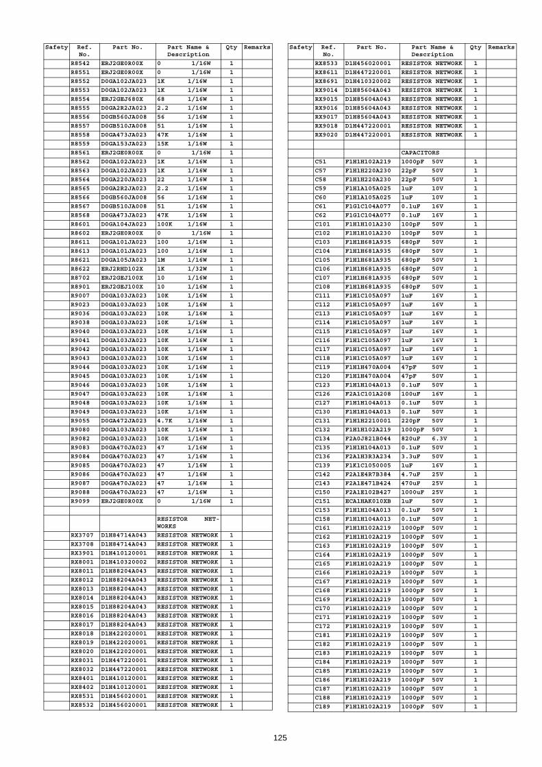
R8542 ERJ2GE0R00X 0 1/16W 1
R8551 ERJ2GE0R00X 0 1/16W 1
R8552 D0GA102JA023 1K 1/16W 1
R8553 D0GA102JA023 1K 1/16W 1
R8554 ERJ2GEJ680X 68 1/16W 1
R8555 D0GA2R2JA023 2.2 1/16W 1
R8556 D0GB560JA008 56 1/16W 1
R8557 D0GB510JA008 51 1/16W 1
R8558 D0GA473JA023 47K 1/16W 1
R8559 D0GA153JA023 15K 1/16W 1
R8561 ERJ2GE0R00X 0 1/16W 1
R8562 D0GA102JA023 1K 1/16W 1
R8563 D0GA102JA023 1K 1/16W 1
R8564 D0GA220JA023 22 1/16W 1
R8565 D0GA2R2JA023 2.2 1/16W 1
R8566 D0GB560JA008 56 1/16W 1
R8567 D0GB510JA008 51 1/16W 1
R8568 D0GA473JA023 47K 1/16W 1
R8601 D0GA104JA023 100K 1/16W 1
R8602 ERJ2GE0R00X 0 1/16W 1
R8611 D0GA101JA023 100 1/16W 1
R8613 D0GA101JA023 100 1/16W 1
R8621 D0GA105JA023 1M 1/16W 1
R8622 ERJ2RHD102X 1K 1/32W 1
R8702 ERJ2GEJ100X 10 1/16W 1
R8901 ERJ2GEJ100X 10 1/16W 1
R9007 D0GA103JA023 10K 1/16W 1
R9023 D0GA103JA023 10K 1/16W 1
R9036 D0GA103JA023 10K 1/16W 1
R9038 D0GA103JA023 10K 1/16W 1
R9040 D0GA103JA023 10K 1/16W 1
R9041 D0GA103JA023 10K 1/16W 1
R9042 D0GA103JA023 10K 1/16W 1
R9043 D0GA103JA023 10K 1/16W 1
R9044 D0GA103JA023 10K 1/16W 1
R9045 D0GA103JA023 10K 1/16W 1
R9046 D0GA103JA023 10K 1/16W 1
R9047 D0GA103JA023 10K 1/16W 1
R9048 D0GA103JA023 10K 1/16W 1
R9049 D0GA103JA023 10K 1/16W 1
R9055 D0GA472JA023 4.7K 1/16W 1
R9080 D0GA103JA023 10K 1/16W 1
R9082 D0GA103JA023 10K 1/16W 1
R9083 D0GA470JA023 47 1/16W 1
R9084 D0GA470JA023 47 1/16W 1
R9085 D0GA470JA023 47 1/16W 1
R9086 D0GA470JA023 47 1/16W 1
R9087 D0GA470JA023 47 1/16W 1
R9088 D0GA470JA023 47 1/16W 1
R9099 ERJ2GE0R00X 0 1/16W 1
RESISTOR NET-WORKS
RX3707 D1H84714A043 RESISTOR NETWORK 1
RX3708 D1H84714A043 RESISTOR NETWORK 1
RX3901 D1H410120001 RESISTOR NETWORK 1
RX8001 D1H410320002 RESISTOR NETWORK 1
RX8011 D1H88204A043 RESISTOR NETWORK 1
RX8012 D1H88204A043 RESISTOR NETWORK 1
RX8013 D1H88204A043 RESISTOR NETWORK 1
RX8014 D1H88204A043 RESISTOR NETWORK 1
RX8015 D1H88204A043 RESISTOR NETWORK 1
RX8016 D1H88204A043 RESISTOR NETWORK 1
RX8017 D1H88204A043 RESISTOR NETWORK 1
RX8018 D1H422020001 RESISTOR NETWORK 1
RX8019 D1H422020001 RESISTOR NETWORK 1
RX8020 D1H422020001 RESISTOR NETWORK 1
RX8031 D1H447220001 RESISTOR NETWORK 1
RX8032 D1H447220001 RESISTOR NETWORK 1
RX8401 D1H410120001 RESISTOR NETWORK 1
RX8402 D1H410120001 RESISTOR NETWORK 1
RX8531 D1H456020001 RESISTOR NETWORK 1
RX8532 D1H456020001 RESISTOR NETWORK 1
Safety Ref. No.
Part No. Part Name & Description
Qty Remarks
RX8533 D1H456020001 RESISTOR NETWORK 1
RX8611 D1H447220001 RESISTOR NETWORK 1
RX8691 D1H410320002 RESISTOR NETWORK 1
RX9014 D1H85604A043 RESISTOR NETWORK 1
RX9015 D1H85604A043 RESISTOR NETWORK 1
RX9016 D1H85604A043 RESISTOR NETWORK 1
RX9017 D1H85604A043 RESISTOR NETWORK 1
RX9018 D1H447220001 RESISTOR NETWORK 1
RX9020 D1H447220001 RESISTOR NETWORK 1
CAPACITORS
C51 F1H1H102A219 1000pF 50V 1
C57 F1H1H220A230 22pF 50V 1
C58 F1H1H220A230 22pF 50V 1
C59 F1H1A105A025 1uF 10V 1
C60 F1H1A105A025 1uF 10V 1
C61 F1G1C104A077 0.1uF 16V 1
C62 F1G1C104A077 0.1uF 16V 1
C101 F1H1H101A230 100pF 50V 1
C102 F1H1H101A230 100pF 50V 1
C103 F1H1H681A935 680pF 50V 1
C104 F1H1H681A935 680pF 50V 1
C105 F1H1H681A935 680pF 50V 1
C106 F1H1H681A935 680pF 50V 1
C107 F1H1H681A935 680pF 50V 1
C108 F1H1H681A935 680pF 50V 1
C111 F1H1C105A097 1uF 16V 1
C112 F1H1C105A097 1uF 16V 1
C113 F1H1C105A097 1uF 16V 1
C114 F1H1C105A097 1uF 16V 1
C115 F1H1C105A097 1uF 16V 1
C116 F1H1C105A097 1uF 16V 1
C117 F1H1C105A097 1uF 16V 1
C118 F1H1C105A097 1uF 16V 1
C119 F1H1H470A004 47pF 50V 1
C120 F1H1H470A004 47pF 50V 1
C123 F1H1H104A013 0.1uF 50V 1
C126 F2A1C101A208 100uF 16V 1
C127 F1H1H104A013 0.1uF 50V 1
C130 F1H1H104A013 0.1uF 50V 1
C131 F1H1H2210001 220pF 50V 1
C132 F1H1H102A219 1000pF 50V 1
C134 F2A0J821B044 820uF 6.3V 1
C135 F1H1H104A013 0.1uF 50V 1
C136 F2A1H3R3A234 3.3uF 50V 1
C139 F1K1C1050005 1uF 16V 1
C142 F2A1E4R7B384 4.7uF 25V 1
C143 F2A1E471B424 470uF 25V 1
C150 F2A1E102B427 1000uF 25V 1
C151 ECA1HAK010XB 1uF 50V 1
C153 F1H1H104A013 0.1uF 50V 1
C158 F1H1H104A013 0.1uF 50V 1
C161 F1H1H102A219 1000pF 50V 1
C162 F1H1H102A219 1000pF 50V 1
C163 F1H1H102A219 1000pF 50V 1
C164 F1H1H102A219 1000pF 50V 1
C165 F1H1H102A219 1000pF 50V 1
C166 F1H1H102A219 1000pF 50V 1
C167 F1H1H102A219 1000pF 50V 1
C168 F1H1H102A219 1000pF 50V 1
C169 F1H1H102A219 1000pF 50V 1
C170 F1H1H102A219 1000pF 50V 1
C171 F1H1H102A219 1000pF 50V 1
C172 F1H1H102A219 1000pF 50V 1
C181 F1H1H102A219 1000pF 50V 1
C182 F1H1H102A219 1000pF 50V 1
C183 F1H1H102A219 1000pF 50V 1
C184 F1H1H102A219 1000pF 50V 1
C185 F1H1H102A219 1000pF 50V 1
C186 F1H1H102A219 1000pF 50V 1
C187 F1H1H102A219 1000pF 50V 1
C188 F1H1H102A219 1000pF 50V 1
C189 F1H1H102A219 1000pF 50V 1
Safety Ref. No.
Part No. Part Name & Description
Qty Remarks
125
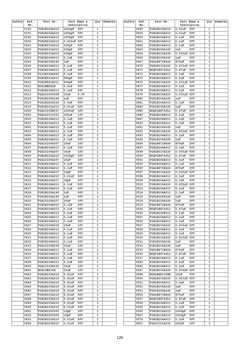
C190 F1H1H102A219 1000pF 50V 1
C191 F1H1H102A219 1000pF 50V 1
C192 F1H1H102A219 1000pF 50V 1
C200 F1H1H223A219 0.022uF 50V 1
C201 F1H1H331A013 330pF 50V 1
C202 F1H1H331A013 330pF 50V 1
C203 F1H1H331A013 330pF 50V 1
C204 F1H1H104A013 0.1uF 50V 1
C205 F1K1H105A149 1uF 50V 1
C206 F1H1H104A013 0.1uF 50V 1
C207 F1H1H104A013 0.1uF 50V 1
C208 F1J1H104A459 0.1uF 50V 1
C209 F1H1H561A013 560pF 50V 1
C210 F1H1H561A013 560pF 50V 1
C211 ECA1HM2R2B 2.2uF 50V 1
C212 F1H1H104A013 0.1uF 50V 1
C213 F2A0J1000008 10uF 6.3V 1
C214 F1K1H105A149 1uF 50V 1
C215 F2A1H3R3A234 3.3uF 50V 1
C216 F1H1H103A219 0.01uF 50V 1
C250 F2A1C102B037 1000uF 16V 1
C251 F2A1C1010033 100uF 16V 1
C400 F1H1H104A013 0.1uF 50V 1
C401 F1H1H104A013 0.1uF 50V 1
C402 F1H1H104A013 0.1uF 50V 1
C403 F1H1H104A013 0.1uF 50V 1
C404 F1H1H104A013 0.1uF 50V 1
C405 F1H1H104A013 0.1uF 50V 1
C406 F2A1C100A207 10uF 16V 1
C407 F1H1H104A013 0.1uF 50V 1
C408 F2A1C100A207 10uF 16V 1
C409 F1H1H102A219 1000pF 50V 1
C410 F2A1C100A207 10uF 16V 1
C411 F1H1H104A013 0.1uF 50V 1
C412 F1H1H104A013 0.1uF 50V 1
C413 F1H1H100A017 10pF 50V 1
C414 F1H1H103A219 0.01uF 50V 1
C415 F1H1H100A017 10pF 50V 1
C416 F1H1H104A013 0.1uF 50V 1
C417 F1H1H104A013 0.1uF 50V 1
C418 F1K1H105A149 1uF 50V 1
C419 F1K1H105A149 1uF 50V 1
C420 F2A1C100A207 10uF 16V 1
C421 F1H1H104A013 0.1uF 50V 1
C423 F1H1H104A013 0.1uF 50V 1
C424 F1H1H104A013 0.1uF 50V 1
C425 F1H1H104A013 0.1uF 50V 1
C426 F1H1H104A013 0.1uF 50V 1
C427 F2A1C100A234 10uF 16V 1
C429 F1H1H104A013 0.1uF 50V 1
C430 F1H1H104A013 0.1uF 50V 1
C431 F1H1H104A013 0.1uF 50V 1
C432 F1H1H104A013 0.1uF 50V 1
C433 F2A1C100A234 10uF 16V 1
C434 F1H1H104A013 0.1uF 50V 1
C436 F1H1H104A013 0.1uF 50V 1
C437 F1H1H104A013 0.1uF 50V 1
C438 F1H1H104A013 0.1uF 50V 1
C439 F2A1C100A234 10uF 16V 1
C441 ECA1CM330B 33uF 16V 1
C442 F1H1H103A219 0.01uF 50V 1
C443 F1H1H103A219 0.01uF 50V 1
C444 F1H1H103A219 0.01uF 50V 1
C445 F1H1H103A219 0.01uF 50V 1
C446 F1H1H103A219 0.01uF 50V 1
C447 F1H1H103A219 0.01uF 50V 1
C448 F1H1H103A219 0.01uF 50V 1
C449 F1H1H103A219 0.01uF 50V 1
C450 F1H1H103A219 0.01uF 50V 1
C451 F1H1H1500009 15pF 50V 1
C452 F1H1H1500009 15pF 50V 1
C453 F1H1H103A219 0.01uF 50V 1
C454 F1H1H103A219 0.01uF 50V 1
Safety Ref. No.
Part No. Part Name & Description
Qty Remarks
C455 F1H1H103A219 0.01uF 50V 1
C456 F1H1H103A219 0.01uF 50V 1
C460 F1H1H104A013 0.1uF 50V 1
C461 F1H1H104A013 0.1uF 50V 1
C462 F1H1H104A013 0.1uF 50V 1
C463 F1K1H105A149 1uF 50V 1
C464 F1H1H333A220 0.033uF 50V 1
C466 F1K1H105A149 1uF 50V 1
C467 F2A1E471B424 470uF 25V 1
C470 F1H1H333A220 0.033uF 50V 1
C471 ECQV1H474JL3 0.47uF 50V 1
C472 F1H1H104A013 0.1uF 50V 1
C473 F1H1H104A013 0.1uF 50V 1
C476 F1H1H333A220 0.033uF 50V 1
C477 F1H1H104A013 0.1uF 50V 1
C478 F1H1H104A013 0.1uF 50V 1
C479 F1H1H333A220 0.033uF 50V 1
C480 F1K1H105A149 1uF 50V 1
C481 F1H1H104A013 0.1uF 50V 1
C482 F1K1H105A149 1uF 50V 1
C485 ECQV1H474JL3 0.47uF 50V 1
C486 F1H1H104A013 0.1uF 50V 1
C487 F1H1H104A013 0.1uF 50V 1
C490 F1H1H104A013 0.1uF 50V 1
C491 F1K1H105A149 1uF 50V 1
C492 F1H1H333A220 0.033uF 50V 1
C493 F1H1H104A013 0.1uF 50V 1
C494 F1K1H105A149 1uF 50V 1
C496 F2A1E471B424 470uF 25V 1
C497 F1H1H104A013 0.1uF 50V 1
C498 F1H1H333A220 0.033uF 50V 1
C500 ECQV1H474JL3 0.47uF 50V 1
C501 F1H1H104A013 0.1uF 50V 1
C502 F1H1H104A013 0.1uF 50V 1
C505 F2A1E471B424 470uF 25V 1
C507 F1H1H333A220 0.033uF 50V 1
C508 F1H1H104A013 0.1uF 50V 1
C509 F1H1H104A013 0.1uF 50V 1
C510 F1H1H333A220 0.033uF 50V 1
C512 F1H1H104A013 0.1uF 50V 1
C514 F1H1H104A013 0.1uF 50V 1
C515 F1K1H105A149 1uF 50V 1
C516 F1K1H105A149 1uF 50V 1
C519 F2A1E471B424 470uF 25V 1
C520 ECQV1H474JL3 0.47uF 50V 1
C522 F1H1H104A013 0.1uF 50V 1
C523 F1H1H104A013 0.1uF 50V 1
C526 F1H1H104A013 0.1uF 50V 1
C527 F1H1H333A220 0.033uF 50V 1
C528 F1H1H104A013 0.1uF 50V 1
C529 F1H1H104A013 0.1uF 50V 1
C530 F1H1H333A220 0.033uF 50V 1
C531 F1K1H105A149 1uF 50V 1
C532 F1K1H105A149 1uF 50V 1
C533 F2A1E471B424 470uF 25V 1
C536 ECQV1H474JL3 0.47uF 50V 1
C537 F1H1H104A013 0.1uF 50V 1
C540 F1H1H104A013 0.1uF 50V 1
C546 F1H1H104A013 0.1uF 50V 1
C547 F1H1H333A220 0.033uF 50V 1
C548 ECA1HAK100XB 10uF 50V 1
C550 F1H1H333A220 0.033uF 50V 1
C551 F1H1H104A013 0.1uF 50V 1
C552 F1K1H105A149 1uF 50V 1
C553 F1K1H105A149 1uF 50V 1
C554 F2A1E471B424 470uF 25V 1
C557 ECQV1H474JL3 0.47uF 50V 1
C558 F1H1H104A013 0.1uF 50V 1
C559 F1H1H104A013 0.1uF 50V 1
C566 F1H1H102A219 1000pF 50V 1
C567 F1H1H102A219 1000pF 50V 1
C574 F1H1H104A013 0.1uF 50V 1
C801 F2A1C101A234 100uF 16V 1
Safety Ref. No.
Part No. Part Name & Description
Qty Remarks
126
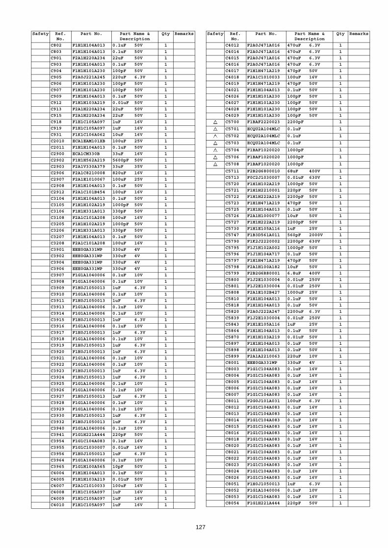
C802 F1H1H104A013 0.1uF 50V 1
C803 F1H1H104A013 0.1uF 50V 1
C901 F2A1H220A234 22uF 50V 1
C903 F1H1H104A013 0.1uF 50V 1
C904 F1H1H101A230 100pF 50V 1
C905 F2A0J221A245 220uF 6.3V 1
C906 F1H1H101A230 100pF 50V 1
C907 F1H1H101A230 100pF 50V 1
C909 F1H1H104A013 0.1uF 50V 1
C912 F1H1H103A219 0.01uF 50V 1
C913 F2A1H220A234 22uF 50V 1
C915 F2A1H220A234 22uF 50V 1
C918 F1H1C105A097 1uF 16V 1
C919 F1H1C105A097 1uF 16V 1
C931 F1K1C106A062 10uF 16V 1
C2010 ECA1EAM101XB 100uF 25V 1
C2011 F1H1H104A013 0.1uF 50V 1
C2900 ECA1CM330B 33uF 16V 1
C2902 F1H1H562A219 5600pF 50V 1
C2903 F2A1V330A379 33uF 35V 1
C2906 F2A1C8210008 820uF 16V 1
C2907 F2A1E1010067 100uF 25V 1
C2908 F1H1H104A013 0.1uF 50V 1
C2912 F2A1C101B454 100uF 16V 1
C3104 F1H1H104A013 0.1uF 50V 1
C3105 F1H1H102A219 1000pF 50V 1
C3106 F1H1H331A013 330pF 50V 1
C3108 F2A1C101A208 100uF 16V 1
C3205 F1H1H102A219 1000pF 50V 1
C3206 F1H1H331A013 330pF 50V 1
C3207 F1H1H104A013 0.1uF 50V 1
C3208 F2A1C101A208 100uF 16V 1
C3901 EEE0GA331WP 330uF 4V 1
C3902 EEE0GA331WP 330uF 4V 1
C3904 EEE0GA331WP 330uF 4V 1
C3906 EEE0GA331WP 330uF 4V 1
C3907 F1G1A1040006 0.1uF 10V 1
C3908 F1G1A1040006 0.1uF 10V 1
C3909 F1H0J1050013 1uF 6.3V 1
C3910 F1G1A1040006 0.1uF 10V 1
C3911 F1H0J1050013 1uF 6.3V 1
C3913 F1G1A1040006 0.1uF 10V 1
C3914 F1G1A1040006 0.1uF 10V 1
C3915 F1H0J1050013 1uF 6.3V 1
C3916 F1G1A1040006 0.1uF 10V 1
C3917 F1H0J1050013 1uF 6.3V 1
C3918 F1G1A1040006 0.1uF 10V 1
C3919 F1H0J1050013 1uF 6.3V 1
C3920 F1H0J1050013 1uF 6.3V 1
C3921 F1G1A1040006 0.1uF 10V 1
C3922 F1G1A1040006 0.1uF 10V 1
C3923 F1H0J1050013 1uF 6.3V 1
C3924 F1H0J1050013 1uF 6.3V 1
C3925 F1G1A1040006 0.1uF 10V 1
C3926 F1G1A1040006 0.1uF 10V 1
C3927 F1H0J1050013 1uF 6.3V 1
C3928 F1G1A1040006 0.1uF 10V 1
C3929 F1G1A1040006 0.1uF 10V 1
C3930 F1H0J1050013 1uF 6.3V 1
C3932 F1H0J1050013 1uF 6.3V 1
C3940 F1G1A1040006 0.1uF 10V 1
C3941 F1G1H221A444 220pF 50V 1
C3954 F1G1C104A083 0.1uF 16V 1
C3955 F1G1C1030007 0.01uF 16V 1
C3956 F1H0J1050013 1uF 6.3V 1
C3964 F1G1A1040006 0.1uF 10V 1
C3965 F1G1H100A565 10pF 50V 1
C4004 F1H1H104A013 0.1uF 50V 1
C4005 F1H1H103A219 0.01uF 50V 1
C4007 F2A1C1010033 100uF 16V 1
C4008 F1H1C105A097 1uF 16V 1
C4009 F1H1C105A097 1uF 16V 1
C4010 F1H1C105A097 1uF 16V 1
Safety Ref. No.
Part No. Part Name & Description
Qty Remarks
C4012 F2A0J471A016 470uF 6.3V 1
C4014 F2A0J471A016 470uF 6.3V 1
C4015 F2A0J471A016 470uF 6.3V 1
C4016 F2A0J471A016 470uF 6.3V 1
C4017 F1H1H471A219 470pF 50V 1
C4018 F2A1C1010033 100uF 16V 1
C4019 F1H1H471A219 470pF 50V 1
C4021 F1H1H104A013 0.1uF 50V 1
C4026 F1H1H101A230 100pF 50V 1
C4027 F1H1H101A230 100pF 50V 1
C4028 F1H1H101A230 100pF 50V 1
C4029 F1H1H101A230 100pF 50V 1
C5700 F1BAF2220023 2200pF 1
C5701 ECQU2A104MLC 0.1uF 1
C5702 ECQU2A104MLC 0.1uF 1
C5703 ECQU2A104MLC 0.1uF 1
C5704 F1BAF1020020 1000pF 1
C5706 F1BAF1020020 1000pF 1
C5708 F1BAF1020020 1000pF 1
C5711 F2B2G6800010 68uF 400V 1
C5713 F0C2J1030007 0.01uF 630V 1
C5720 F1H1H102A219 1000pF 50V 1
C5721 F1H1H2210001 220pF 50V 1
C5722 F1H1H222A219 2200pF 50V 1
C5723 F1H1H471A219 470pF 50V 1
C5725 F1H1H104A013 0.1uF 50V 1
C5726 F2A1H1000077 10uF 50V 1
C5727 F1H1H222A219 2200pF 50V 1
C5730 F1H1E105A116 1uF 25V 1
C5747 F1B3D561A011 560pF 2000V 1
C5790 F1K2J2220002 2200pF 630V 1
C5795 F1J1H102A002 1000pF 50V 1
C5796 F1J1H104A717 0.1uF 50V 1
C5797 F1H1H471A219 470pF 50V 1
C5798 F2A1H100A182 10uF 50V 1
C5799 F2B2G6R80001 6.8uF 400V 1
C5800 F1J2E1030004 0.01uF 250V 1
C5801 F1J2E1030004 0.01uF 250V 1
C5808 F2A1E102B427 1000uF 25V 1
C5810 F1H1H104A013 0.1uF 50V 1
C5818 F1H1H104A013 0.1uF 50V 1
C5820 F2A0J222A247 2200uF 6.3V 1
C5839 F1J2E1030004 0.01uF 250V 1
C5843 F1H1E105A116 1uF 25V 1
C5864 F1H1H104A013 0.1uF 50V 1
C5870 F1H1H103A219 0.01uF 50V 1
C5897 F1H1H104A013 0.1uF 50V 1
C5898 F1H1H104A013 0.1uF 50V 1
C5899 F2A1A2210063 220uF 10V 1
C8001 EEE0GA331WP 330uF 4V 1
C8003 F1G1C104A083 0.1uF 16V 1
C8004 F1G1C104A083 0.1uF 16V 1
C8005 F1G1C104A083 0.1uF 16V 1
C8006 F1G1C104A083 0.1uF 16V 1
C8007 F1G1C104A083 0.1uF 16V 1
C8011 F2G0J101A031 100uF 6.3V 1
C8012 F1G1C104A083 0.1uF 16V 1
C8013 F1G1C104A083 0.1uF 16V 1
C8014 F1G1C104A083 0.1uF 16V 1
C8015 F1G1C104A083 0.1uF 16V 1
C8016 F1G1C104A083 0.1uF 16V 1
C8018 F1G1C104A083 0.1uF 16V 1
C8020 F1G1C104A083 0.1uF 16V 1
C8021 F1G1C104A083 0.1uF 16V 1
C8022 F1G1C104A083 0.1uF 16V 1
C8023 F1G1C104A083 0.1uF 16V 1
C8024 F1G1C104A083 0.1uF 16V 1
C8026 F1G1C104A083 0.1uF 16V 1
C8051 F1H0J1050013 1uF 6.3V 1
C8052 F1G1A1040006 0.1uF 10V 1
C8053 F1G1C104A083 0.1uF 16V 1
C8054 F1G1H221A444 220pF 50V 1
Safety Ref. No.
Part No. Part Name & Description
Qty Remarks
127
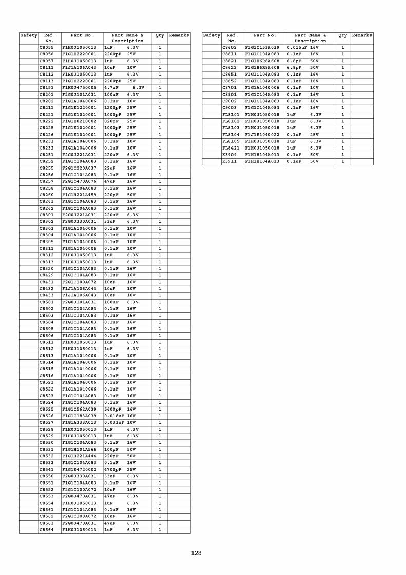
C8055 F1H0J1050013 1uF 6.3V 1
C8056 F1G1E2220001 2200pF 25V 1
C8057 F1H0J1050013 1uF 6.3V 1
C8111 F1J1A106A043 10uF 10V 1
C8112 F1H0J1050013 1uF 6.3V 1
C8113 F1G1E2220001 2200pF 25V 1
C8151 F1H0J4750005 4.7uF 6.3V 1
C8201 F2G0J101A031 100uF 6.3V 1
C8202 F1G1A1040006 0.1uF 10V 1
C8211 F1G1E1220001 1200pF 25V 1
C8221 F1G1E1020001 1000pF 25V 1
C8222 F1G1E8210002 820pF 25V 1
C8225 F1G1E1020001 1000pF 25V 1
C8226 F1G1E1020001 1000pF 25V 1
C8231 F1G1A1040006 0.1uF 10V 1
C8232 F1G1A1040006 0.1uF 10V 1
C8251 F2G0J221A031 220uF 6.3V 1
C8252 F1G1C104A083 0.1uF 16V 1
C8255 F2G1C220A037 22uF 16V 1
C8256 F1G1C104A083 0.1uF 16V 1
C8257 F2G1C470A076 47uF 16V 1
C8258 F1G1C104A083 0.1uF 16V 1
C8260 F1G1H221A459 220pF 50V 1
C8261 F1G1C104A083 0.1uF 16V 1
C8262 F1G1C104A083 0.1uF 16V 1
C8301 F2G0J221A031 220uF 6.3V 1
C8302 F2G0J330A031 33uF 6.3V 1
C8303 F1G1A1040006 0.1uF 10V 1
C8304 F1G1A1040006 0.1uF 10V 1
C8305 F1G1A1040006 0.1uF 10V 1
C8311 F1G1A1040006 0.1uF 10V 1
C8312 F1H0J1050013 1uF 6.3V 1
C8313 F1H0J1050013 1uF 6.3V 1
C8320 F1G1C104A083 0.1uF 16V 1
C8429 F1G1C104A083 0.1uF 16V 1
C8431 F2G1C100A072 10uF 16V 1
C8432 F1J1A106A043 10uF 10V 1
C8433 F1J1A106A043 10uF 10V 1
C8501 F2G0J101A031 100uF 6.3V 1
C8502 F1G1C104A083 0.1uF 16V 1
C8503 F1G1C104A083 0.1uF 16V 1
C8504 F1G1C104A083 0.1uF 16V 1
C8505 F1G1C104A083 0.1uF 16V 1
C8506 F1G1C104A083 0.1uF 16V 1
C8511 F1H0J1050013 1uF 6.3V 1
C8512 F1H0J1050013 1uF 6.3V 1
C8513 F1G1A1040006 0.1uF 10V 1
C8514 F1G1A1040006 0.1uF 10V 1
C8515 F1G1A1040006 0.1uF 10V 1
C8516 F1G1A1040006 0.1uF 10V 1
C8521 F1G1A1040006 0.1uF 10V 1
C8522 F1G1A1040006 0.1uF 10V 1
C8523 F1G1C104A083 0.1uF 16V 1
C8524 F1G1C104A083 0.1uF 16V 1
C8525 F1G1C562A039 5600pF 16V 1
C8526 F1G1C183A039 0.018uF 16V 1
C8527 F1G1A333A013 0.033uF 10V 1
C8528 F1H0J1050013 1uF 6.3V 1
C8529 F1H0J1050013 1uF 6.3V 1
C8530 F1G1C104A083 0.1uF 16V 1
C8531 F1G1H101A566 100pF 50V 1
C8532 F1G1H221A444 220pF 50V 1
C8533 F1G1C104A083 0.1uF 16V 1
C8541 F1G1E4720002 4700pF 25V 1
C8550 F2G0J330A031 33uF 6.3V 1
C8551 F1G1C104A083 0.1uF 16V 1
C8552 F2G1C100A072 10uF 16V 1
C8553 F2G0J470A031 47uF 6.3V 1
C8554 F1H0J1050013 1uF 6.3V 1
C8561 F1G1C104A083 0.1uF 16V 1
C8562 F2G1C100A072 10uF 16V 1
C8563 F2G0J470A031 47uF 6.3V 1
C8564 F1H0J1050013 1uF 6.3V 1
Safety Ref. No.
Part No. Part Name & Description
Qty Remarks
C8602 F1G1C153A039 0.015uF 16V 1
C8611 F1G1C104A083 0.1uF 16V 1
C8621 F1G1H6R8A608 6.8pF 50V 1
C8622 F1G1H6R8A608 6.8pF 50V 1
C8651 F1G1C104A083 0.1uF 16V 1
C8652 F1G1C104A083 0.1uF 16V 1
C8701 F1G1A1040006 0.1uF 10V 1
C8901 F1G1C104A083 0.1uF 16V 1
C9002 F1G1C104A083 0.1uF 16V 1
C9003 F1G1C104A083 0.1uF 16V 1
FL8101 F1H0J1050018 1uF 6.3V 1
FL8102 F1H0J1050018 1uF 6.3V 1
FL8103 F1H0J1050018 1uF 6.3V 1
FL8104 F1J1E1040022 0.1uF 25V 1
FL8105 F1H0J1050018 1uF 6.3V 1
FL8421 F1H0J1050018 1uF 6.3V 1
K3909 F1H1H104A013 0.1uF 50V 1
K3911 F1H1H104A013 0.1uF 50V 1
Safety Ref. No.
Part No. Part Name & Description
Qty Remarks
128

MMH0909
129