Embed Size (px)
Citation preview
GB
CLASS 1LASER PRODUCT
COMPACT
DIGITAL AUDIO
Service Manual
ServiceServiceServiceServiceService
FW-C155/22/25
TABLE OF CONTENTSPage
Location of PCBs & Version variations ......................1-2
Technical Specifications .............................................1-3
Measurement setup ....................................................1-4
Service Aids, Safety Instruction, etc ...........................1-5
Preparations & Controls .............................................2-1
Disassembly Instructions & Service positions ...........3-1
Service Test Programs ...............................................3-3
Set Block diagram ......................................................4-1
Set Wiring diagram .....................................................5-1
Front & Combi Board ..................................................... 6
ECO Power Board ......................................................... 7
Tape Mechanism............................................................ 9
3CDC-LLC-MCD1 Module ........................................... 10
Set Mechanical Exploded view & parts list ................. 11
© Copyright 2001 Philips Consumer Electronics B.V. Eindhoven, The NetherlandsAll rights reserved. No part of this publication may be reproduced, stored in a retrieval system ortransmitted, in any form or by any means, electronic, mechanical, photocopying, or otherwisewithout the prior permission of Philips.
Published by SL 0301 Service Audio Printed in The Netherlands Subject to modification
Mini System
3140 785 32440
Version 1.0
1-2
ECO POWER BOARD
LOCATION OF PRINTED CIRCUIT BOARDS
/21 /22 /34
Incredible Surround
Karaoke
News
RDS
Rotary Encoder (volume control)
Jog Shuttle
Voltage Selector x
Aux Input
Digital Output
Headphone Socket x x x
Line Output
Subwoofer Output
Surround Output
Matrix Surround Loudspeakers
Standby - Clock Display x x x
Standby - Dark
VERSION VARIATIONS:
Type /Versions: FW-C155
Features &Board in used:
COMBI BOARD
FRONTBOARD
CD BOARD
/37
x
x
ECO Power Standby (Clock Display Off)
ECO6 Tuner Board - System Cenelec
x
x
ECO6 Tuner Board - System Non-Cenelec x x x
/25
x
x
x
x
1-3
SPECIFICATIONS
GENERAL:
Mainsvoltage :230V ±10%
Mains frequency : 50Hz
Power consumption : ≤ 11W at Standby
≤ 0.5W at ECO Standby
30W Active
Clock accuracy : < 4 seconds per day
Dimension centre unit
: 265 x 310 x 330mm
TUNER:
FM
Tuning range : 87.5-108MHz
Grid : 50kHz
IF frequency : 10.7MHz ± 20kHz
Aerial input : 75W coaxial
Sensitivity at 26dB S/N : < 22mV
Selectivity at 300kHz bandwidth : > 25dB
Image rejection,98MHz : > 80dB
Distortion at RF=1mV, dev. 75kHz : < 3%
-3dB Limiting point : < 23.5mV
Crosstalk at RF=1mV, dev. 40kHz : > 18dB
MW
Tuning range : 531-1602kHz
Grid : 9kHz
IF frequency : 450kHz ± 1kHz
Aerial input : Frame aerial, 18.1 µH
Sensitivity at 26dB S/N : < 4.4mV/M
Selectivity at 300kHz bandwidth : > 18dB
IF rejection : > 45dB
Image rejection : > 28dB
Distortion at RF=50mV, m=80% : < 5%
AMPLIFIER:
Output power 1) : 2 x 3.5W ±1dB
Frequency response within -3dB : 50Hz-15kHz
Dynamic Bass Boost : DBB1, DBB2, DBB3, DBB Off 2)
Digital Sound Control : Jazz, Techno, Optimal, Rock 2)
Headphone output at 32W : 900mV ± 1dB (max Vol.)
CASSETTE RECORDER:
Number of track : 2 x 2 stereo
Tape speed : 4.76 cm/sec +2.5/-1.5%
Wow and flutter : < 0.35% DIN
Fast-wind/rewind time C60 : 130 sec
Bias system : 75kHz ±5kHz
Rec/Pb frequency response within 8dB : 80Hz - 10kHz
Signal to noise ratio (A-weighted) : ≥ 48dBA
COMPACT DISC:
Measurement done at output conn. of the CDC module.
Frequency response within ± 1.5dB : 20Hz - 20kHz
Output level (in Vrms) : 550mV, Zout = 100W
Signal/Noise ratio (A-weighted) : > 80dBA
Distortion at 1kHz : < 0.003%
Channel unbalance at 1kHz : ±1dB
Channel separation at 1kHz : > 60dB
De-emphasis : 0 or 15/50 mS (Switched by subcode
on the disc)
1) 3W, 1 kHz, 10% THD
2) Frequency response in each setting is software controlled.
Weight (w/o speakers) : 4.6Kg
Frequency response : 80 - 12500Hz (8dB)
LF Generator e.g. PM5110
Recorder
Use Universal Test Cassette CrO2 SBC419 4822 397 30069
LEVEL METERe.g. Sennheiser UPM550
with FF-filter
S/N and distortion metere.g. Sound Technology ST1700B
L
R
DUT
or Universal Test Cassette Fe SBC420 4822 397 30071
LEVEL METERe.g. Sennheiser UPM550
with FF-filter
S/N and distortion metere.g. Sound Technology ST1700B
L
R
DUT
CD
Use Audio Signal Disc(replaces test disc 3)
SBC429 4822 397 30184
Bandpass250Hz-15kHz
e.g. 7122 707 48001LF Voltmeter
e.g. PM2534DUT
S/N and distortion meter e.g. Sound Technology ST1700B
Frame aeriale.g. 7122 707 89001
Tuner AM (MW,LW)
To avoid atmospheric interference all AM-measurements have to be carried out in a Faraday´s cage.Use a bandpass filter (or at least a high pass filter with 250Hz) to eliminate hum (50Hz, 100Hz).
RF Generator e.g. PM5326
Ri=
50Ω
Bandpass250Hz-15kHz
e.g. 7122 707 48001LF Voltmeter
e.g. PM2534DUT
RF Generator e.g. PM5326
S/N and distortion meter e.g. Sound Technology ST1700B
Use a bandpass filter to eliminate hum (50Hz, 100Hz) and disturbance from the pilottone (19kHz, 38kHz).
Ri=
50Ω
Tuner FM
MEASUREMENT SETUP
1-4
1-5
SERVICE AIDS
Service Tools:
Universal Torx driver holder .................................. 4822 395 91019
Torx bit T10 150mm ............................................. 4822 395 50456
Torx driver set T6 - T20 ......................................... 4822 395 50145
Torx driver T10 extended ...................................... 4822 395 50423
Cassette:
SBC419 Test cassette CrO2 ................................. 4822 397 30069
SBC420 Test cassette Fe ..................................... 4822 397 30071
MTT150 Dolby level 200nWb/M ............................ 4822 397 30271
Compact Disc:
SBC426/426A Test disc 5 + 5A ............................ 4822 397 30096
SBC442 Audio Burn-in Test disc 1kHz ................. 4822 397 30155
SBC429 Audio Signals disc .................................. 4822 397 30184
Dolby Pro-logic Test Disc ...................................... 4822 395 10216
ESD Equipment:
Anti-static table mat - large 1200x650x1.25mm ... 4822 466 10953
Anti-static table mat - small 600x650x1.25mm ..... 4822 466 10958
Anti-static wristband .............................................. 4822 395 10223
Connector box (1MΩ) ............................................ 4822 320 11307
Extension cable
(to connect wristband to conn. box) .................. 4822 320 11305
Connecting cable
(to connect table mat to conn. box) .................. 4822 320 11306
Earth cable (to connect product to mat or box) .... 4822 320 11308
Complete kit ESD3
(combining all above products) ......................... 4822 320 10671
Wristband tester .................................................... 4822 344 13999
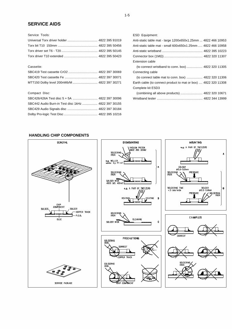
HANDLING CHIP COMPONENTS
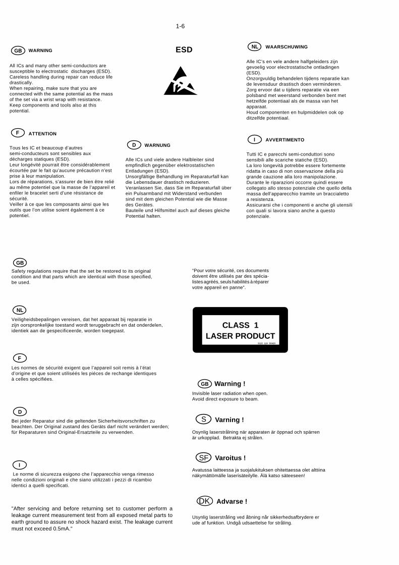
1-6
GB WARNING
All ICs and many other semi-conductors aresusceptible to electrostatic discharges (ESD).Careless handling during repair can reduce lifedrastically.When repairing, make sure that you areconnected with the same potential as the massof the set via a wrist wrap with resistance.Keep components and tools also at thispotential.
F ATTENTION
Tous les IC et beaucoup d’autressemi-conducteurs sont sensibles auxdécharges statiques (ESD).Leur longévité pourrait être considérablementécourtée par le fait qu’aucune précaution n’estprise à leur manipulation.Lors de réparations, s’assurer de bien être reliéau même potentiel que la masse de l’appareil etenfiler le bracelet serti d’une résistance desécurité.Veiller à ce que les composants ainsi que lesoutils que l’on utilise soient également à cepotentiel.
ESD
D WARNUNG
Alle ICs und viele andere Halbleiter sindempfindlich gegenüber elektrostatischenEntladungen (ESD).Unsorgfältige Behandlung im Reparaturfall kandie Lebensdauer drastisch reduzieren.Veranlassen Sie, dass Sie im Reparaturfall überein Pulsarmband mit Widerstand verbundensind mit dem gleichen Potential wie die Massedes Gerätes.Bauteile und Hilfsmittel auch auf dieses gleichePotential halten.
NL WAARSCHUWING
Alle IC’s en vele andere halfgeleiders zijngevoelig voor electrostatische ontladingen(ESD).Onzorgvuldig behandelen tijdens reparatie kande levensduur drastisch doen verminderen.Zorg ervoor dat u tijdens reparatie via eenpolsband met weerstand verbonden bent methetzelfde potentiaal als de massa van hetapparaat.Houd componenten en hulpmiddelen ook opditzelfde potentiaal.
I AVVERTIMENTO
Tutti IC e parecchi semi-conduttori sonosensibili alle scariche statiche (ESD).La loro longevità potrebbe essere fortementeridatta in caso di non osservazione della piùgrande cauzione alla loro manipolazione.Durante le riparazioni occorre quindi esserecollegato allo stesso potenziale che quello dellamassa dell’apparecchio tramite un braccialettoa resistenza.Assicurarsi che i componenti e anche gli utensilicon quali si lavora siano anche a questopotenziale.
“Pour votre sécurité, ces documentsdoivent être utilisés par des spécia-listes agréés, seuls habilités à réparervotre appareil en panne”.
GBSafety regulations require that the set be restored to its originalcondition and that parts which are identical with those specified,be used.
NL
Veiligheidsbepalingen vereisen, dat het apparaat bij reparatie inzijn oorspronkelijke toestand wordt teruggebracht en dat onderdelen,identiek aan de gespecificeerde, worden toegepast.
F
Les normes de sécurité exigent que l’appareil soit remis à l’étatd’origine et que soient utiliséés les piéces de rechange identiquesà celles spécifiées.
D
Bei jeder Reparatur sind die geltenden Sicherheitsvorschriften zubeachten. Der Original zustand des Geräts darf nicht verändert werden;für Reparaturen sind Original-Ersatzteile zu verwenden.
I
Le norme di sicurezza esigono che l’apparecchio venga rimessonelle condizioni originali e che siano utilizzati i pezzi di ricambioidentici a quelli specificati.
"After servicing and before returning set to customer perform aleakage current measurement test from all exposed metal parts toearth ground to assure no shock hazard exist. The leakage currentmust not exceed 0.5mA."
CLASS 1LASER PRODUCT
3122 110 03420
GB Warning !Invisible laser radiation when open.Avoid direct exposure to beam.
S Varning !
Osynlig laserstrålning när apparaten är öppnad och spärrenär urkopplad. Betrakta ej strålen.
SF Varoitus !
Avatussa laitteessa ja suojalukituksen ohitettaessa olet alttiinanäkymättömälle laserisäteilylle. Älä katso säteeseen!
DK Advarse !
Usynlig laserstråling ved åbning når sikkerhedsafbrydere erude af funktion. Undgå udsaettelse for stråling.
PREPARATIONS AND CONTROLS
2-1
Pre
par
atio
ns
Rea
r co
nn
ecti
on
s
The
typ
e p
late
is l
ocat
ed a
t th
e re
ar o
f th
esy
stem
.
APo
wer
Befo
re c
onne
ctin
g th
e A
C p
ow
er c
ord
to t
hew
all o
utle
t, en
sure
tha
t al
l oth
er c
onne
ctio
nsha
ve b
een
mad
e.
WA
RN
ING
!–
For
opti
mal
per
form
ance
, use
onl
y th
eor
igin
al p
ower
cab
le.
–N
ever
mak
e or
cha
nge
any
conn
ecti
ons
wit
h th
e p
ower
sw
itch
ed o
n.
BA
nte
nn
as C
on
nec
tio
n
Con
nect
the
sup
plie
d A
M lo
op a
nten
na a
nd F
Man
tenn
a to
the
res
pect
ive
term
inal
s.
Adj
ust
the
posit
ion
of t
he a
nten
na fo
r op
timal
rec
eptio
n.
AM
An
ten
na
Fix
th
e cl
aw
to t
he
slo
t
P
ositi
on t
he a
nten
na a
s fa
r as
pos
sible
from
a T
V,
VC
R o
r ot
her
radi
atio
n so
urce
.
R+
–
L
spea
ker
(rig
ht)
spea
ker
(left)
FM
wire
ant
enna
AM
loop
an
tenn
a
A
B
C
+
–
AC
pow
er c
ord
VO
LTA
GE
SE
LEC
TOR
110V
-12
7V22
0V-
240V
For
user
s in
the
U.K
.: p
leas
e fo
llow
the
inst
ruct
ions
on
pag
e 2-
3.
Pre
par
atio
ns
FM
An
ten
na
Fo
r be
tter
FM
ste
reo
rece
ptio
n, c
onne
ct a
nou
tdoo
r FM
ant
enna
to
the
FM A
NT
ENN
Ate
rmin
al.
CS
pea
kers
Co
nn
ecti
on
Fro
nt
Sp
eake
rsC
onne
ct th
e sp
eake
r w
ires
to t
he S
PEA
KER
Ste
rmin
als,
right
spe
aker
to
"R" a
nd le
ft sp
eake
r to
"L",
colo
ured
(m
arke
d) w
ire t
o "+
" and
bla
ck(u
nmar
ked)
wire
to
"-".
1
2
Fu
lly in
sert
the
strip
ped
port
ion
of t
he s
peak
erw
ire in
to t
he t
erm
inal
as
sho
wn.
Not
es:
–F o
r op
timal
sou
nd p
erfo
rman
ce, u
se th
esu
pplie
d sp
eake
rs.
–D
o no
t con
nect
mor
e th
an o
ne s
peak
er to
any
one
pair
of +
/- s
peak
er te
rmin
als.
–D
o no
t con
nect
spe
aker
s w
ith im
peda
nce
low
erth
an th
e sp
eake
rs s
uppl
ied.
Ple
ase
refe
r to
the
SPEC
IFIC
ATIO
NS
sect
ion
of th
is m
anua
l.
Inse
rtin
g b
atte
ries
into
th
ere
mo
te c
on
tro
lIn
sert
two
batt
erie
s ty
pe R
03 o
r A
AA
(no
tsu
pplie
d) in
to t
he r
emot
e co
ntro
l with
the
corr
ect
pola
r ity
as
indi
cate
d by
the
"+" a
nd"-
" sym
bols
insid
e th
e ba
tter
y co
mpa
rtm
ent.
CA
UT
ION
!–
Rem
ove
bat
teri
es if
the
y ar
e ex
haus
ted
or w
ill n
ot b
e us
ed f
or a
long
tim
e.–
Do
not
use
old
and
new
or
diff
eren
tty
pes
of
batt
erie
s in
com
bina
tion
.–
Bat
teri
es c
onta
in c
hem
ical
sub
stan
ces,
so
they
sho
uld
be d
isp
osed
off
pro
per
ly.
PREPARATIONS AND CONTROLS
2-2
TU
NE
RT
AP
E
CD
1C
D 2
CD
3
BA
ND
TA
PE
1 • 2
DY
NA
MIC
BA
SS
BO
OS
T
DIG
ITA
LS
OU
ND
CO
NT
RO
LM
AS
TE
R V
OL
UM
E
ST
OP
•CL
EA
R / D
EM
O S
TO
P
SE
AR
CH
•TU
NIN
G
SE
AR
CH
•TU
NIN
G
PL
AY
• PA
US
E
PR
ES
ET
CL
OC
K•T
IME
RD
IM M
OD
EP
RO
GR
AM
P
RE
SE
TP
RE
V/
NE
XT
/
OP
EN
/C
LO
SE
DIS
CC
HA
NG
E
CD
STA
ND
BY
ON
MIN
I H
IFI
SY
ST
EM
FW
-C1
55
DC3
CH
AN
GE
R
CD
/CD
- R/C
D- R
W C
OM
PAT
IBL
E
PLA
Y/R
EC
EC
O
PO
WE
R
VO
LU
ME
DS
C
TECHNO
OP
TIM
AL
JAZZ
KC
OR
1 762 4 5 8 9 0!* & ^ % $ # @
3
£
4
DSC
DB
BM
UTE
2CD
1/2
/3
REPE
A TSH
UFF
LESL
EEP
TUN
ERTA
PE 1
/2D
MU
TEN
EWS/
TAá
á
ëí
ÅÉ
Ç
VOL
( ) ^ 5
%™
2 8
¡2 #
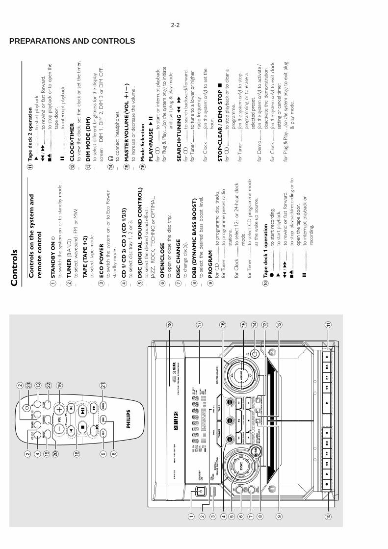
Co
ntr
ols
Co
ntr
ols
on
th
e sy
stem
an
dre
mo
te c
on
tro
l
1S
TA
ND
BY
ON
y–
to s
witc
h th
e sy
stem
on
or t
o st
andb
y m
ode
.
2T
UN
ER
(B
AN
D)
–to
sel
ect
wav
eban
d : F
M o
r M
W.
TA
PE
(T
AP
E 1
•2)
–to
sel
ect
tape
mod
e.
3 –to
sw
itch
the
syst
em o
n or
to
Eco
Pow
erst
andb
y m
ode
.
4C
D 1
/ CD
2/ C
D 3
(C
D 1
/2/3
)–
to s
elec
t di
sc t
ray
1, 2
or
3.
5D
SC
(D
IGIT
AL
SO
UN
D C
ON
TR
OL
)–
to s
elec
t th
e de
sired
sou
nd e
ffect
:JA
ZZ
, RO
CK,
TEC
HN
O o
r O
PTIM
AL.
6O
PE
N/C
LO
SE
–to
ope
n or
clo
se t
he d
isc t
ray.
7D
ISC
CH
AN
GE
–to
cha
nge
disc
(s).
8D
BB
(D
YN
AM
IC B
AS
S B
OO
ST
)–
to s
elec
t th
e de
sired
bas
s bo
ost
leve
l.
9P
RO
GR
AM
for
CD
........
........
. to
prog
ram
me
disc
tra
cks.
for T
uner
........
..... t
o pr
ogra
mm
e pr
eset
rad
iost
atio
ns.
for
Clo
ck....
........
to s
elec
t 12-
or
24-h
our
cloc
km
ode
.fo
r Tim
er....
........
. to
sele
ct C
D p
rogr
amm
e m
ode
as t
he w
ake
up s
ourc
e.
0T
ape
dec
k 1
op
erat
ion
â....
........
........
...... t
o st
art
reco
rdin
g.É
........
........
........
.. to
star
t pla
ybac
k.à
/ á
........
.......
to r
ewin
d or
fast
for
war
d.70
........
........
........
to s
top
play
back
/rec
ordi
ng o
r to
open
the
tap
e do
or.
Å....
........
........
......
to in
terr
upt
play
back
or
reco
rdin
g.
!T
ape
dec
k 2
op
erat
ion
É....
........
........
......t
o st
art p
layb
ack.
à / á
........
.......
to r
ewin
d or
fast
for
war
d.70
........
........
........
to s
top
play
back
or
to o
pen
the
tape
doo
r .Å
........
........
........
.. to
inte
rrup
t pl
ayba
ck.
@C
LO
CK
•TIM
ER
–to
vie
w t
he c
lock
, se
t th
e cl
ock
or s
et t
he ti
mer
.
#D
IM M
OD
E (
DIM
)–
to s
elec
t di
ffere
nt b
right
ness
for
the
disp
lay
scre
en
: DIM
1, D
IM 2
, DIM
3 o
r D
IM O
FF.
$n
–to
con
nect
hea
dpho
nes.
%M
AS
TE
R V
OL
UM
E
(VO
L +
/-)
–to
incr
ease
or
decr
ease
the
vol
ume
.
^M
od
e S
elec
tio
n
PL
AY
•PA
US
E ÉÅ
for
CD
........
........
. to
star
t or
inte
rrup
t pl
ayba
ck.
for
Plug
& P
lay…
(on
the
syst
em o
nly)
to
initi
ate
and
star
t plu
g &
pla
y m
ode
.
SE
AR
CH
•TU
NIN
G à
á
for
CD
........
........
. to
sear
ch b
ackw
ard/
forw
ard.
for T
uner
........
..... t
o tu
ne t
o a
low
er o
r hi
gher
radi
o fr
eque
ncy.
for
Clo
ck....
........
(on
the
syst
em o
nly)
to
set
the
hour
.
ST
OP
•CL
EA
R /
DE
MO
ST
OP
Çfo
r C
D....
........
.....t
o st
op p
layb
ack
or t
o cl
ear
apr
ogra
mm
e.
for T
uner
........
.....(
on th
e sy
stem
onl
y) t
o st
oppr
ogra
mm
ing
or t
o er
ase
ase
lect
ed p
rese
t.fo
r D
emo
........
...(o
n th
e sy
stem
onl
y) t
o ac
tivat
e/
deac
tivat
e th
e de
mon
stra
tion.
for
Clo
ck....
........
(on
the
syst
em o
nly)
to
exit
cloc
kse
ttin
g or
can
cel t
imer
.fo
r Pl
ug &
Pla
y…(o
n th
e sy
stem
onl
y) t
o ex
it pl
ug&
pla
y m
ode
.
EC
O P
OW
ER
PREPARATIONS AND CONTROLS
2-3
PR
EV
í /
PR
ES
ET
4N
EX
T ë
/ P
RE
SE
T3
for
CD
........
........
. to
skip
to
the
begi
nnin
g of
the
curr
ent,
pre
viou
s, or
nex
t tr
ack.
for T
uner
........
..... t
o se
lect
a p
rese
t r a
dio
stat
ion.
for
Clo
ck....
........
(on
the
syst
em o
nly)
to
set
the
min
ute
.
&D
isp
lay
scre
en–
to v
iew
the
cur
rent
sta
tus
of t
he s
yste
m.
*D
isc
tray
(R
EP
EA
T–
to p
layb
ack
trac
k(s)
/disc
(s)/
prog
ram
me
repe
ated
ly.
)S
HU
FF
LE
–to
pla
ybac
k al
l ava
ilabl
e di
scs
and
thei
r tr
acks
/pr
ogra
mm
e in
ran
dom
ord
er.
¡M
UT
E–
to in
terr
upt
or r
esum
e so
und
repr
oduc
tion.
™S
LE
EP
–to
act
ivat
e/de
activ
ate
or s
et t
he s
leep
tim
er.
£B
–to
sw
itch
the
syst
em t
o st
andb
y m
ode
.–
to s
witc
h th
e sy
stem
to
Eco
Pow
er s
tand
bym
ode
.
Not
es f
or re
mot
e co
ntro
l:–
Firs
t, se
lect
the
sou
rce
you
wis
h to
cont
rol b
y p
ress
ing
one
of t
he s
ourc
e se
lect
keys
on
the
rem
ote
cont
rol (
CD
1/2
/3 o
rT
UN
ER
, for
exa
mp
le).
–T
hen
sele
ct t
he d
esir
ed f
unct
ion
( É,
í, ë
, fo
r ex
amp
le).
Co
ntr
ols
Imp
orta
nt
not
es fo
r u
sers
in t
he
U.K
.
Mai
ns
plu
gT
his
appa
ratu
s is
fitte
d w
ith a
n ap
prov
ed 1
3A
mp
plug
. To
cha
nge
a fu
se in
thi
s ty
pe o
f plu
gpr
ocee
d as
fol
low
s:
1R
emov
e fu
se c
over
and
fuse
.
2Fi
x ne
w fu
se w
hich
sho
uld
be a
BS1
362
5 A
mp,
A.S
.T.A
. or
BSI a
ppro
ved
type
.
3R
efit
the
fuse
cov
er.
If th
e fit
ted
plug
is n
ot s
uita
b le
for
your
soc
ket
outle
ts,
it sh
ould
be
cut
off a
nd a
n ap
prop
riat
epl
ug f
itted
in it
s pl
ace.
If th
e m
ains
plu
g co
ntai
ns a
fuse
, thi
s sh
ould
have
a v
alue
of 5
Am
p. If
a p
lug
with
out
a fu
seis
used
, th
e fu
se a
t th
e di
strib
utio
n bo
ard
shou
ld n
ot b
e gr
eate
r th
an 5
Am
p.
Not
e: T
hese
vere
d pl
ug m
ust b
e di
spos
ed o
f to
avoi
d a
poss
ible
sho
ck h
azar
d sh
ould
it b
ein
sert
ed in
to a
13
Amp
sock
et e
lsew
here
.
How
to
co
nn
ect
a p
lug
The
wire
s in
the
mai
ns le
ad a
re c
olou
red
with
the
follo
win
g co
de: b
lue
= n
eutr
al (
N),
bro
wn
= li
ve (
L).
¶A
s th
ese
colo
urs
ma
y no
t co
rre
spon
d w
ith t
heco
lour
mar
king
s id
entif
ying
the
ter
min
als
inyo
ur p
lug,
pro
ceed
as
follo
ws:
–C
onne
ct t
he b
lue
wire
to
the
term
inal
mar
ked
N o
r co
lour
ed b
lack
.–
Con
nect
the
bro
wn
wire
to
the
term
inal
mar
ked
L or
col
oure
d re
d.–
Do
not
conn
ect
eith
er w
ire t
o th
e ea
rth
term
inal
in t
he p
lug,
mar
ked
E (o
r e)
orco
lour
ed g
reen
(or
gre
en a
nd y
ello
w).
Befo
re r
epla
cing
the
plu
g co
ver,
mak
e ce
rtai
nth
at t
he c
ord
grip
is c
lam
ped
over
the
she
ath
of t
he le
ad -
not
sim
ply
over
the
tw
o w
ires.
Co
pyri
ght
in t
he
U.K
.R
ecor
ding
and
pla
ybac
k of
mat
eria
l may
requ
ire c
onse
nt. S
ee C
opyr
ight
Act
195
6 an
dT
he P
erfo
rmer
’s Pr
otec
tion
Act
s 19
58 t
o 19
72.
No
rge
Type
skilt
fin
nes
på a
ppar
aten
s un
ders
ide.
Obs
erve
r: N
ettb
ryte
ren
er s
ekun
dert
innk
ople
t. D
en in
neby
gde
netd
elen
er
derf
or ik
ke f
rako
ple
t ne
ttet
så
leng
eap
par
atet
er
tils
lutt
et n
ettk
onta
kten
.
For
å re
duse
re fa
ren
for
bran
n el
ler
elek
trisk
støt
, ska
l app
arat
et ik
ke u
tset
tes
for
regn
elle
rfu
ktig
het.
Ita
liaD
ICH
IAR
AZ
ION
E D
I C
ON
FO
RM
ITA
’
Si d
ichi
ara
che
l’app
arec
chio
FW
-C71
7 Ph
ilips
rispo
nde
alle
pre
scr iz
ioni
del
l’art
. 2 c
omm
a 1
del D
.M. 2
8 A
gost
o 19
95 n
. 54
8.
Fatt
o a
Eind
hove
n
Phili
ps C
onsu
mer
Ele
ctro
nics
Philip
s, G
lasla
an 2
5616
JB E
indh
oven
,
The
Net
herla
nds
CA
UT
ION
Use
of
cont
rols
or
adju
stm
ents
or
per
form
ance
of
pro
cedu
res
othe
r th
anhe
rein
may
res
ult
in h
azar
dous
radi
atio
n ex
pos
ure
or o
ther
uns
afe
oper
atio
n.
Mai
nte
nan
ce
Cle
anin
g th
e C
abin
et
Use
a s
oft
clot
h sli
ghtly
moi
sten
ed w
ith a
mild
dete
rgen
t so
lutio
n. D
o no
t us
e a
solu
tion
cont
aini
ng a
lcoh
ol, s
piri
ts, a
mm
onia
or
abra
sives
.
Cle
anin
g D
iscs
¶W
hen
a di
sc b
ecom
es d
irty
,cl
ean
it w
ith a
cle
anin
g cl
oth.
Wip
e th
e di
sc fr
om t
he c
entr
eou
t. D
o no
t w
ipe
in a
circ
ular
mot
ion.
¶D
o no
t us
e so
lven
ts s
uch
asbe
nzen
e, t
hinn
er, c
omm
erci
ally
avai
labl
e cl
eane
rs, o
r an
tista
tic s
pray
inte
nded
for
anal
ogue
rec
ords
.
Cle
anin
g th
e d
isc
len
s
Afte
r pr
olon
ged
use,
dir
t or
dus
t m
ayac
cum
ulat
e at
the
disc
lens
. T
o en
sure
goo
dpl
ayba
ck q
ualit
y, cl
ean
the
disc
lens
with
Phi
lips
CD
Len
s C
lean
er o
r an
y co
mm
erci
ally
ava
ilabl
ecl
eane
r. Fo
llow
the
inst
ruct
ions
sup
plie
d w
ith t
hecl
eane
r.
Cle
anin
g th
e H
ead
s an
d t
he
Tap
e P
ath
s
To e
nsur
e go
od r
ecor
ding
and
pla
ybac
k qu
ality
,cl
ean
the
head
s A
, the
cap
stan
(s) B
, and
pres
sure
rol
ler(
s) C
afte
r ev
ery
50 h
ours
of
tape
ope
ratio
n.
Use
a c
otto
n sw
ab s
light
ly m
oist
ened
with
clea
ning
flui
d or
alc
ohol
.
You
also
can
cle
an t
he h
eads
by
pla
ying
acl
eani
ng t
ape
once
.
CC
BB
A
Dem
agn
etis
ing
the
hea
ds
¶U
se a
dem
agne
tisin
g ta
pe a
vaila
ble
at y
our
deal
er.
Tro
ubl
esh
oo
tin
g
WA
RN
ING
Und
er n
o ci
rcum
stan
ces
shou
ld y
ou t
ry t
o re
pai
r th
e sy
stem
you
rsel
f, a
s th
is w
ill in
valid
ate
the
war
rant
y. D
o no
t op
en t
he s
yste
m a
s th
ere
is a
ris
k of
ele
ctri
c sh
ock.
If a
faul
t oc
curs
, fir
st c
heck
the
poi
nts
liste
d be
low
bef
ore
taki
ng t
he s
yste
m f
or r
epai
r. If
you
are
unab
le t
o re
med
y a
pro
blem
by
follo
win
g th
ese
hint
s, c
onsu
lt y
our
deal
er o
r se
rvic
e ce
ntre
.
Pro
blem
So
luti
on
CD
OP
ER
AT
ION
“NO DISC
” is
dis
pla
yed
.–
Inse
rt a
disc
.–
Che
ck if
the
disc
is in
sert
ed u
psid
e do
wn.
–W
ait
until
the
moi
stur
e co
nden
satio
n at
the
lens
has
clea
red.
–R
epla
ce o
r cl
ean
the
disc
, see
“M
aint
enan
ce”.
“DISC NOT FINALIZED
” is
dis
pla
yed
.–
Use
a f
inal
ised
CD
-R(W
) or
CD
-R.
Tro
ub
lesh
oo
tin
g
RA
DIO
RE
CE
PT
ION
Rad
io r
ecep
tio
n is
po
or.
–If
the
signa
l is
too
wea
k, a
djus
t th
e an
tenn
a or
conn
ect
an e
xter
nal a
nten
na f
or b
ette
r re
cept
ion.
–In
crea
se t
he d
istan
ce b
etw
een
the
Min
i HiF
iSy
stem
and
you
r TV
or
VC
R.
TA
PE
OP
ER
AT
ION
/RE
CO
RD
ING
Rec
ord
ing
or
pla
ybac
k ca
nn
ot
be
mad
e.–
Cle
an d
eck
par t
s, s
ee “
Mai
nten
ance
”.–
Use
onl
y N
OR
MA
L (IE
C I)
tape
.–
App
ly a
pie
ce o
f adh
esiv
e ta
pe o
ver
the
miss
ing
tab
spac
e.
Th
e ta
pe
dec
k d
oo
r ca
nn
ot
op
en.
–R
emo
ve a
nd r
econ
nect
the
AC
po
wer
plu
g an
dsw
itch
on t
he s
yste
m a
gain
.
GE
NE
RA
L
Th
e sy
stem
do
es n
ot
reac
t w
hen
bu
tto
ns
–R
emo
ve a
nd r
econ
nect
the
AC
po
wer
plu
g an
dar
e p
ress
ed.
switc
h on
the
sys
tem
aga
in.
So
un
d c
ann
ot
be
hea
rd o
r is
of
po
or
–A
djus
t th
e vo
lum
e.
qu
alit
y.–
Disc
onne
ct t
he h
eadp
hone
s.–
Che
ck t
hat
the
spea
kers
are
con
nect
ed c
orre
ctly.
–C
heck
if t
he s
trip
ped
spea
ker
wire
is c
lam
ped.
Th
e le
ft a
nd
rig
ht
sou
nd
ou
tpu
ts a
re–
Che
ck t
he s
peak
er c
onne
ctio
ns a
nd lo
catio
n.re
vers
ed.
Th
e r e
mo
te c
on
tro
l do
es n
ot
fun
ctio
n–
Sele
ct t
he s
ourc
e (C
D o
r T
UN
ER,
for
exam
ple)
pro
per
ly.
befo
re p
ress
ing
the
func
tion
butt
on (É
,í,ë
).–
Red
uce
the
dist
ance
bet
wee
n th
e re
mot
e co
ntro
lan
d th
e sy
stem
.–
Inse
rt t
he b
atte
rie
s w
ith t
heir
pola
ritie
s(+
/– s
igns
) al
igne
d as
indi
cate
d.–
Rep
lace
the
bat
ter i
es.
–Po
int
the
rem
ote
cont
rol i
n th
e di
rect
ion
of t
hesy
stem
’s IR
sen
sor.
Th
e ti
mer
is n
ot
wo
rkin
g.–
Set
the
cloc
k co
rrec
tly.
–Pr
ess
TIM
ER O
N/O
FF t
o sw
itch
on t
he t
imer
.–
If re
cord
ing
is in
pro
gres
s, st
op r
ecor
ding
.
No
t al
l lig
hte
d b
utt
on
s ar
e sh
owin
g lig
ht.
–Pr
ess
DIS
PLA
Y t
o se
lect
NO
RM
AL
or M
OD
E 1
disp
lay m
ode
.
Th
e C
lock
/Tim
er s
etti
ng
is e
rase
d.
–Po
wer
has
bee
n in
terr
upte
d or
the
pow
er c
ord
has
been
disc
onne
cted
. Res
et t
he c
lock
/tim
er.
Th
e sy
stem
dis
pla
ys fe
atu
res
–Pr
ess
and
hold
DEM
O S
TOP Ç
on t
he s
yste
mau
tom
atic
ally
an
d b
utt
on
s st
art
flash
ing.
to s
witc
h of
f the
dem
onst
ratio
n.
MAINTENANCE AND TROUBLESHOOTING
2-4
2-1 2-1
DISMANTLING INSTRUCTIONS
Dismantling of the Lens Cassette
1) Uncatch 4 catches along the edge of the Cassette door
(pos 5) as shown in figure 1 and 2 to remove the Lens
cassette (pos 2).
Figure 2: Left Cassette door
Figure 1
1) Loosen the 4 screws, slide Cover top (pos 30) towards the
rear and remove it upwards.
2) Loosen 3 screws slide the Panel right (pos 26) towards the
rear and remove it outwards. Do likewise for the Panel left
(pos 27).
3) Push the gear slowly towards the front as shown in figure
Dismantling the 3CDC Module
3 until the CDC tray starts to move out of the Front Cabinet
(pos 8). The CDC tray is now disengage and can be pulled
out completely.
4) Remove the Cover Tray (pos 29) as shown in figure 4.
5) Loosen 4 screws A to remove the CDC Module (pos 28) as
shown in figure 3.
A
A
A
Turn the Gear towards the Fronttill the CDC Tray starts to open
Figure 3
Figure 4
C1
Press Inwards
Pull RearPanel out
1
2
Figure 5
Dismantling of the Panel Rear
1) Loosen 6 screws C on the Panel rear (pos 24).
2) Press the 2 catches C1 inwards and dismantle the Panel
rear by pulling it towards the rear.
2-2 2-2
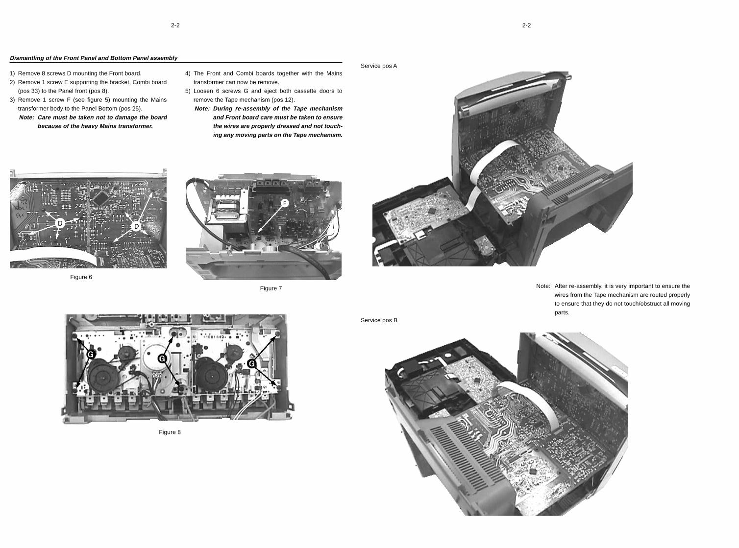
Service pos A
Service pos B
Note: After re-assembly, it is very important to ensure the
wires from the Tape mechanism are routed properly
to ensure that they do not touch/obstruct all moving
parts.
Dismantling of the Front Panel and Bottom Panel assembly
Figure 6
Figure 7
Figure 8
1) Remove 8 screws D mounting the Front board.
2) Remove 1 screw E supporting the bracket, Combi board
(pos 33) to the Panel front (pos 8).
3) Remove 1 screw F (see figure 5) mounting the Mains
transformer body to the Panel Bottom (pos 25).
Note: Care must be taken not to damage the boardbecause of the heavy Mains transformer.
4) The Front and Combi boards together with the Mains
transformer can now be remove.
5) Loosen 6 screws G and eject both cassette doors to
remove the Tape mechanism (pos 12).
Note: During re-assembly of the Tape mechanismand Front board care must be taken to ensurethe wires are properly dressed and not touch-ing any moving parts on the Tape mechanism.
3-1 3-1
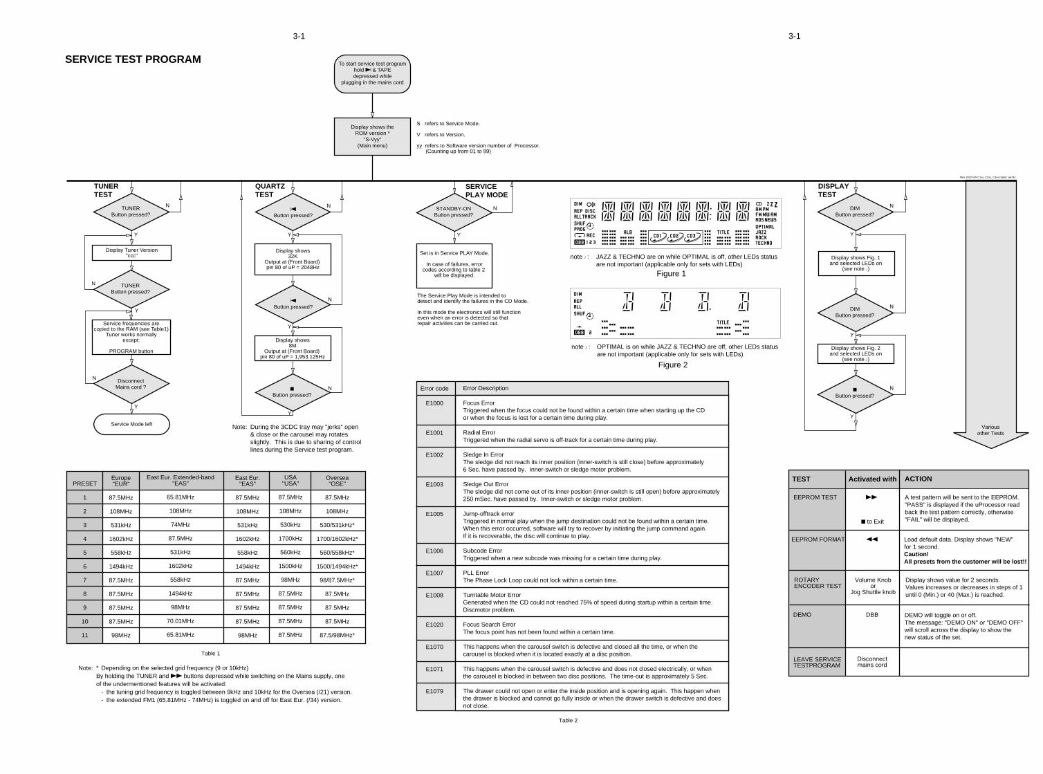
Variousother Tests
Activated with ACTIONTEST
QEEPROM FORMAT Load default data. Display shows "NEW" for 1 second.Caution!All presets from the customer will be lost!!
Disconnectmains cord
LEAVE SERVICETESTPROGRAM
R
9 to Exit
EEPROM TEST A test pattern will be sent to the EEPROM."PASS" is displayed if the uProcessor readback the test pattern correctly, otherwise"FAIL" will be displayed.
Volume Knobor
Jog Shuttle knob
ROTARYENCODER TEST
Display shows value for 2 seconds.Values increases or decreases in steps of 1until 0 (Min.) or 40 (Max.) is reached.
DBBDEMO DEMO will toggle on or off.The message: "DEMO ON" or "DEMO OFF"will scroll across the display to show thenew status of the set.
STANDBY-ONButton pressed?
Y
N
Set is in Service PLAY Mode.
The Service Play Mode is intended todetect and identify the failures in the CD Mode.
In this mode the electronics will still functioneven when an error is detected so thatrepair activities can be carried out.
SERVICEPLAY MODE
In case of failures, errorcodes according to table 2
will be displayed.
OButton pressed?
Y
Y
Y
N
N
N
OButton pressed?
9Button pressed?
Display shows8M
Output at (Front Board) pin 80 of uP = 1,953.125Hz
Display shows32K
Output at (Front Board) pin 80 of uP = 2048Hz
QUARTZTEST
Note: During the 3CDC tray may "jerks" open& close or the carousel may rotatesslightly. This is due to sharing of controllines during the Service test program.
TUNERButton pressed?
DisconnectMains cord ?
Y
N
N
Y
Service frequencies arecopied to the RAM (see Table1)
Tuner works normallyexcept:
PROGRAM button
Service Mode left
TUNERTEST
Display Tuner Version"ccc"
TUNERButton pressed?
N
Y
PRESET
1
2
3
4
5
6
7
8
9
10
11
Europe"EUR"
87.5MHz
108MHz
531kHz
1602kHz
558kHz
1494kHz
87.5MHz
87.5MHz
87.5MHz
87.5MHz
98MHz
East Eur."EAS"
87.5MHz
108MHz
531kHz
1602kHz
558kHz
1494kHz
87.5MHz
87.5MHz
87.5MHz
87.5MHz
98MHz
USA"USA"
87.5MHz
108MHz
530kHz
1700kHz
560kHz
1500kHz
98MHz
87.5MHz
87.5MHz
87.5MHz
87.5MHz
Oversea"OSE"
87.5MHz
108MHz
530/531kHz*
1700/1602kHz*
560/558kHz*
1500/1494kHz*
98/87.5MHz*
87.5MHz
87.5MHz
87.5MHz
87.5/98MHz*
Table 1
East Eur. Extended-band"EAS"
65.81MHz
108MHz
74MHz
87.5MHz
531kHz
1602kHz
558kHz
1494kHz
98MHz
70.01MHz
65.81MHz
Note: * Depending on the selected grid frequency (9 or 10kHz)By holding the TUNER and R buttons depressed while switching on the Mains supply, oneof the undermentioned features will be activated:
- the tuning grid frequency is toggled between 9kHz and 10kHz for the Oversea (/21) version.- the extended FM1 (65.81MHz - 74MHz) is toggled on and off for East Eur. (/34) version.
Y
N
Y
N
Y
N
DIMButton pressed?
DIMButton pressed?
9Button pressed?
DISPLAYTEST
Display shows Fig. 2and selected LEDs on
(see note 2)
Display shows Fig. 1and selected LEDs on
(see note 1)Figure 1
Figure 2
note 2 : OPTIMAL is on while JAZZ & TECHNO are off, other LEDs statusare not important (applicable only for sets with LEDs)
note 1 : JAZZ & TECHNO are on while OPTIMAL is off, other LEDs statusare not important (applicable only for sets with LEDs)
Table 2
Error code
E1000
E1001
E1002
E1003
E1005
E1006
E1007
E1008
E1020
E1070
E1071
E1079
Error Description
Focus ErrorTriggered when the focus could not be found within a certain time when starting up the CDor when the focus is lost for a certain time during play.
Radial ErrorTriggered when the radial servo is off-track for a certain time during play.
Sledge In ErrorThe sledge did not reach its inner position (inner-switch is still close) before approximately6 Sec. have passed by. Inner-switch or sledge motor problem.
Sledge Out ErrorThe sledge did not come out of its inner position (inner-switch is still open) before approximately250 mSec. have passed by. Inner-switch or sledge motor problem.
Jump-offtrack errorTriggered in normal play when the jump destination could not be found within a certain time.When this error occurred, software will try to recover by initiating the jump command again.If it is recoverable, the disc will continue to play.
Subcode ErrorTriggered when a new subcode was missing for a certain time during play.
PLL ErrorThe Phase Lock Loop could not lock within a certain time.
Turntable Motor ErrorGenerated when the CD could not reached 75% of speed during startup within a certain time.Discmotor problem.
Focus Search ErrorThe focus point has not been found within a certain time.
This happens when the carousel switch is defective and closed all the time, or when thecarousel is blocked when it is located exactly at a disc position.
This happens when the carousel switch is defective and does not closed electrically, or whenthe carousel is blocked in between two disc positions. The time-out is approximately 5 Sec.
The drawer could not open or enter the inside position and is opening again. This happen whenthe drawer is blocked and cannot go fully inside or when the drawer switch is defective and doesnot close.
To start service test programhold P & TAPEdepressed while
plugging in the mains cord
Display shows theROM version *
"S-Vyy"(Main menu)
S refers to Service Mode.
V refers to Version.
yy refers to Software version number of Processor. (Counting up from 01 to 99)
SERVICE TEST PROGRAM
Mini 2002 FW-C1xx, C2xx, C3xx Dated: wk141
4-1
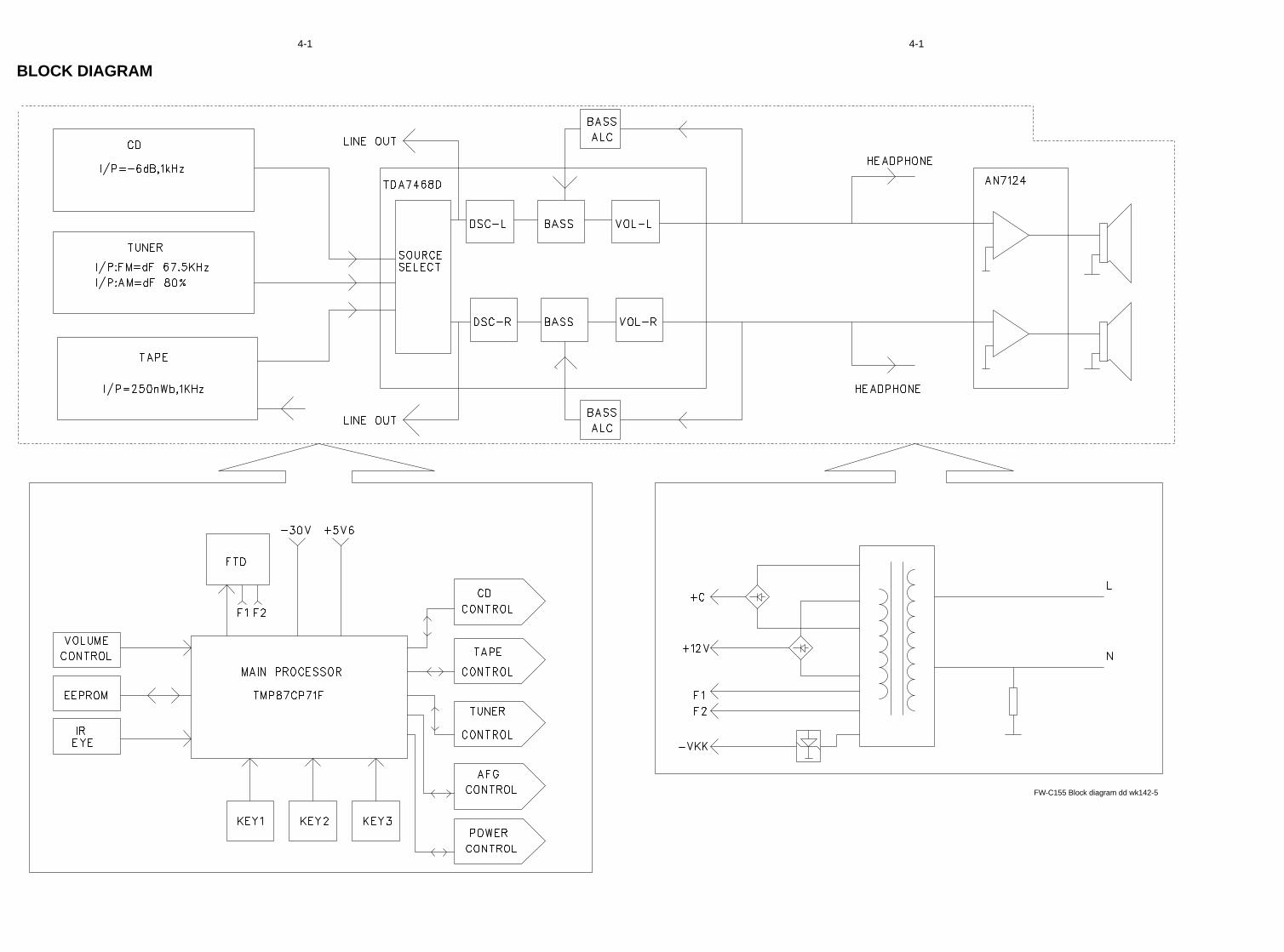
BLOCK DIAGRAM
4-1
FW-C155 Block diagram dd wk142-5
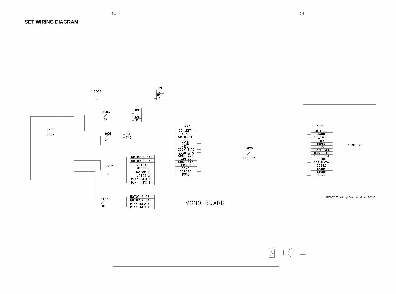
5-1
SET WIRING DIAGRAM
5-1
FW-C155 Wiring Diagram dd wk142-5
6-16-1
COMBI & FRONT BOARDS
TABLE OF CONTENTS
FTD Display pin connection .......................................... 6-1
Tape Adjustment & Mesurement ................................... 6-2
Tuner Adjustment Table ................................................. 6-2
Combi part Component Layout ..................................... 6-3
Combi part SMD Layout ................................................ 6-4
Tuner Circuit .................................................................. 6-5
Supply & Power Amplifier Circuit ................................... 6-6
Tape Circuit .................................................................... 6-7
Front Circuit ................................................................... 6-8
Front part SMD Layout .................................................. 6-9
Front part Component Layout ..................................... 6-10
TDA7468 & TMP87CN71 Internal Block diagram ....... 6-11
Electrical parts list ........................................................ 6-11
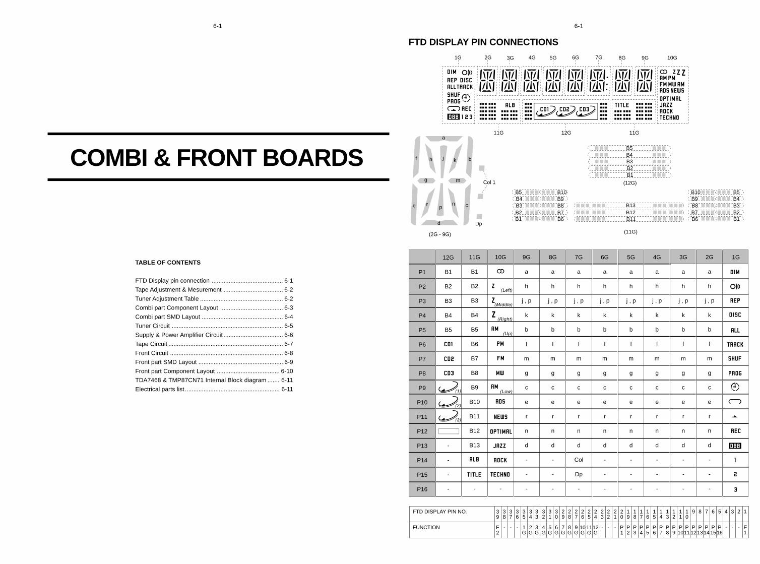
FTD DISPLAY PIN CONNECTIONS
FTD DISPLAY PIN NO.
FUNCTION
34
2G
35
1G
36
-
37
-
38
-
39
F2
33
3G
31
5G
30
6G
29
7G
28
8G
32
4G
26
10G
25
11G
24
12G
23
-
27
9G
22
-
21
-
20
P1
19
P2
18
P3
17
P4
16
P5
14
P7
13
P8
12
P9
11
P10
15
P6
10
P11
9
P12
8
P13
7
P14
6
P15
5
P16
4
-
3
-
2
-
1
F1
4G
a
h
j , p
k
b
f
m
g
c
e
r
n
d
-
-
-
10G
-
6G
a
h
j , p
k
b
f
m
g
c
e
r
n
d
-
-
-
12G
B1
B2
B3
B4
B5
-
-
-
-
5G
a
h
j , p
k
b
f
m
g
c
e
r
n
d
-
-
-
3G
a
h
j , p
k
b
f
m
g
c
e
r
n
d
-
-
-
1G7G
a
h
j , p
k
b
f
m
g
c
e
r
n
d
Col
Dp
-
8G
a
h
j , p
k
b
f
m
g
c
e
r
n
d
-
-
-
9G
a
h
j , p
k
b
f
m
g
c
e
r
n
d
-
-
-
11G
B1
B2
B3
B4
B5
B6
B7
B8
B9
B10
B11
B12
B13
-
P1
P2
P3
P4
P5
P6
P7
P8
P9
P10
P11
P12
P13
P14
P15
P16
2G
a
h
j , p
k
b
f
m
g
c
e
r
n
d
-
-
-
(Left)
(Middle)
(Right)
(Up)
(Low)(1)
(2)
(3)
B5B4
B1B2B3
B10B9B8B7B6
B5B4B3B2B1
B10B9B8B7B6
B13B12B11
B5B4B3B2B1
Col 1
(11G)
(12G)
a
khf bj
Dp
n
g m
pe cr
d
(2G - 9G)
1G 2G 10G
11G
8G 9G3G 4G 5G 6G 7G
12G 11G
6-26-2
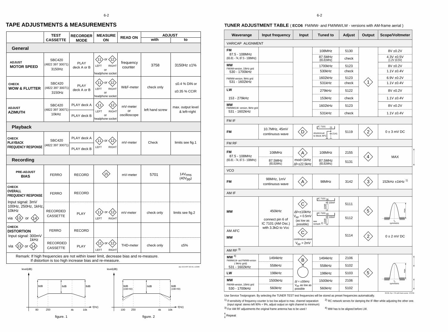
VARICAP ALIGNMENT
FM RF
FM IF
VCO
AM IF
AM RF 3)
108MHz
87.5MHz(65.81MHz)
87.5MHz(65.81MHz)
87.5MHz(65.81MHz)
279kHz
153kHz
1602kHz
531kHz
5130
check
5122
check
5123
check
8V ±0.2V
4.3V ±0.5V(1.2V ±0.5V)
8V ±0.2V
1.1V ±0.4V
8V ±0.2V
1.1V ±0.4V
1494kHz
558kHz
560kHz 5102
1500kHz
5103198kHz
1494kHz
558kHz
560kHz
1500kHz
198kHz
2106
5102
2106
3142 152kHz ±1kHz 1)98MHz
5112
MAX
FM 87.5 - 108MHz(65.81 - 74, 87.5 - 108MHz)
LW
153 - 279kHz
MWFM/MW/LW- version, 9kHz grid 531 - 1602kHz
1700kHz
530kHz
5123
check
8V ±0.2V
1.1V ±0.4V
1602kHz
531kHz
5123
check
6.9V ±0.2V
1.1V ±0.4V
108MHz 108MHz 2155
5131
MWFM/AM-version, 10kHz grid 530 - 1700kHz
FM
MW
LW
98MHz, 1mVcontinuous wave
450kHz
connect pin 6 ofIC 7101 (AM Osc.)with 3.3kΩ to Vcc
Use Service Testprogram. By selecting the TUNER TEST test frequencies will be stored as preset frequencies automatically.
4
1
3
5
5
A
A
5119FM10.7MHz, 45mVcontinuous wave 2D
mod=1kHz∆f=±22.5kHz
1) If sensitivity of frequency counter is too low adjust to max. channel separation (input signal: stereo left 90% + 9%, adjust output on right channel to minimum)
Repeat
ECO6, Sys + PA with frame aerial, 070799
TUNER ADJUSTMENT TABLE ( ECO6 FM/MW- and FM/MW/LW - versions with AM-frame aerial )
∆f=±10kHzVRF = 0.5mV
C
see remark 2)
220R
100nF36IC 7101
220R
100nF40IC 7101
2141shortcircuitto block AFC
21IC 7101
max
.
symmetricfo
AM AFC
MWC
continuous wave
VRF = 2mV
5111
5114 2 0 ± 2 mV DC
0 ± 3 mV DC
MW 4)
FM/MW/LW- and FM/MW-version ( 9kHz grid)
531 - 1602kHz
B
∆f = ±30kHzVRF as low aspossible
max
.
symmetricfoMW
FM/AM-version, 10kHz grid
530 - 1700kHz
3) For AM RF adjustments the original frame antenna has to be used !
2) RC network serves for damping the IF-filter while adjusting the other one.
4) MW has to be aligned before LW.
Waverange Input frequency Input Tuned to Adjust Output Scope/Voltmeter
FM 87.5 - 108MHz(65.81 - 74, 87.5 - 108MHz)
FM/MW-version, 9kHz grid 531 - 1602kHz
(as low aspossible)
Playback
LEFT RIGHT
mV-meter Check limits see fig.1SBC420
(4822 397 30071)
CHECKPLAYBACKFREQUENCY RESPONSE
General
TESTCASSETTE
RECORDER MODE
MEASURE ON
READ ONADJUST
with to
ADJUST
MOTOR SPEED
SBC420(4822 397 30071)
3150Hz
PLAYdeck A or B
PLAYdeck A or B
or
LEFT RIGHTfrequency counter 3758
SBC420(4822 397 30071)
3150HzLEFT RIGHT
SBC420(4822 397 30071)
10kHzLEFT RIGHT
PLAY deck A
W&F-meter check only
mV-meteror
oscilloscope
left hand screwmax. output level
& left=right
CHECK
WOW & FLUTTER
ADJUST
AZIMUTH
3150Hz ±1%
≤0.4 % DIN or
≤0.35 % CCIR
figure. 1
f(Hz)
level(dB)
8dB6dB
10k4k25080
8dB
orheadphone socket
orheadphone socket
orheadphone socket
PLAY deck B
PLAY deck A
PLAY deck B
figure. 2
f(Hz)
level(dB)
6dB
10k4k250100
8dB(10dB HSD)
8dB(10dB HSD)
adj. ECO MTF DD AS, 110399
11 12
or11 12
11 12
or11 12
Recording
mV-meter 5701
RECORDEDCASSETTE
LEFT RIGHT
PLAY mV-meter check only limits see fig.2
FERRO
FERRO
RECORDEDCASSETTE
LEFT RIGHTPLAY THD-meter check only ≤5%
PRE-ADJUST
BIAS
Input signal: 3mV100Hz, 250Hz, 1kHz,10kHz
via or
CHECKOVERALLFREQUENCY RESPONSE
CHECK
DISTORTIONInput signal: 300mV
1kHz
via or
Remark: If high frequencies are not within lower limit, decrease bias and re-measure. If distortion is too high increase bias and re-measure.
14Vrms(40Vpp)
RECORD
RECORD
RECORD
FERRO 15
or11 12
or11 1213 14
13 14
TAPE ADJUSTMENTS & MEASUREMENTS
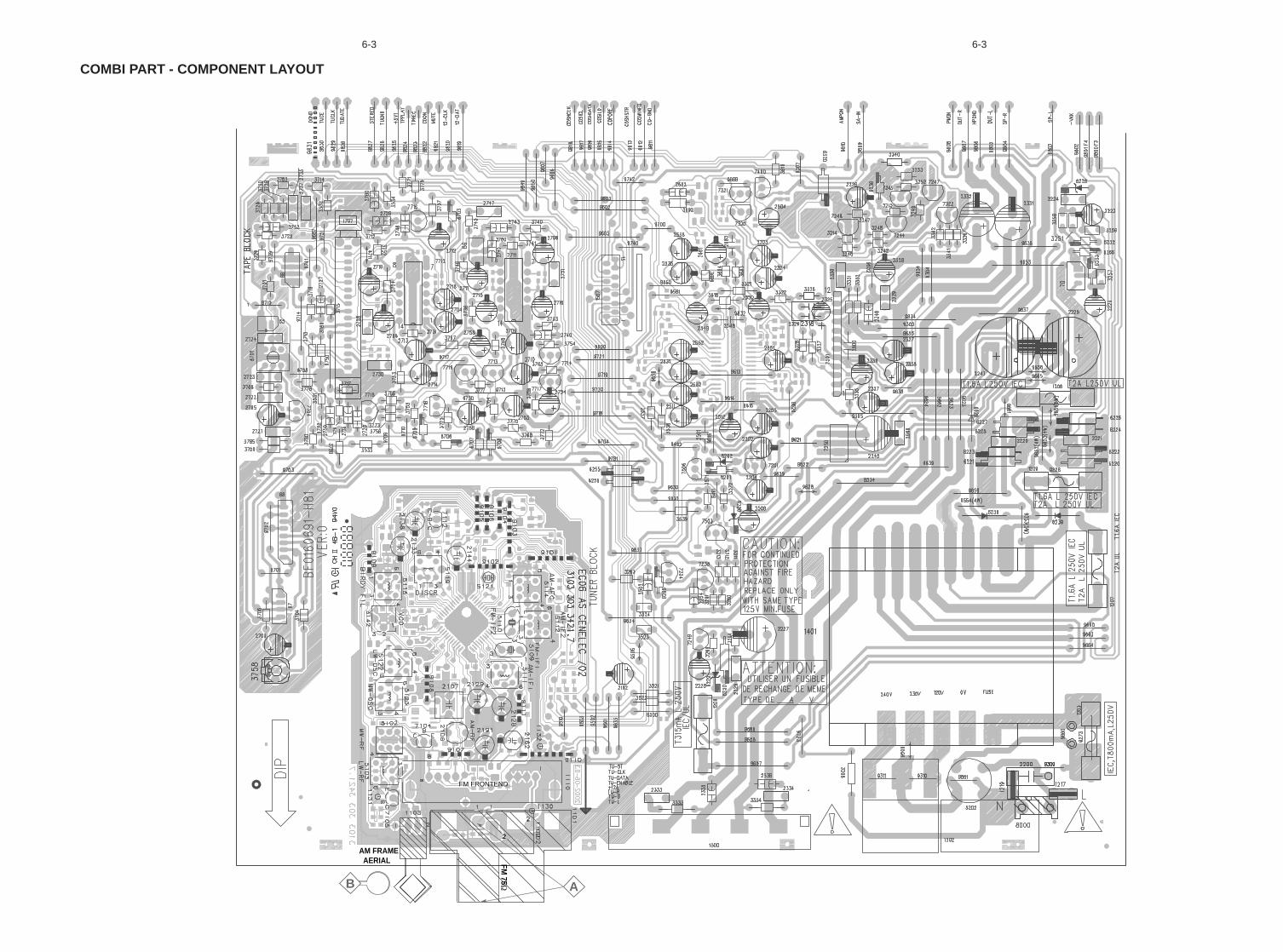
6-36-3
AM FRAME AERIAL FM
75ΩFM FRONTEND
B A
COMBI PART - COMPONENT LAYOUT
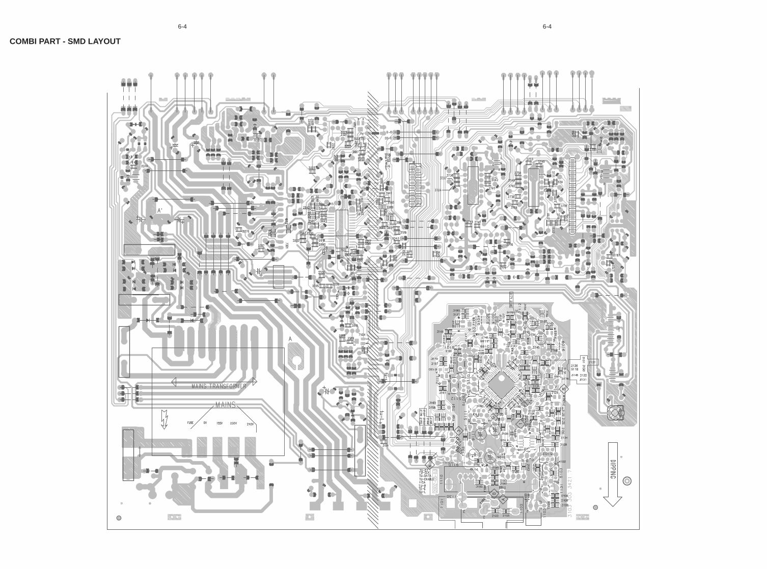
6-4 6-4
COMBI PART - SMD LAYOUT
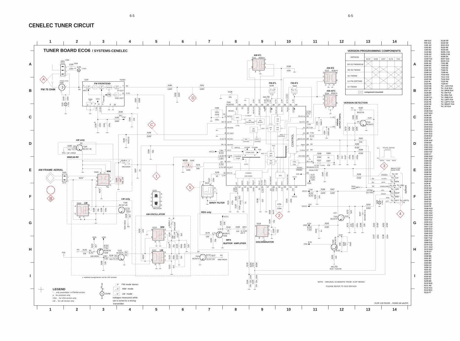
CENELEC TUNER CIRCUIT
6-5 6-5
MIXER
varic
ap
FM FRONTEND
GND
PRE-
SCALER
MULTI-
PLEXER
VSTABA
AM-IF
MONO/
XTAL
AGC
CO
NT
RO
L
OSC
AM DET
AMOSC
AGC
VCC2
AGC
PUMP
AMMIXER
DECODER
CHARGE
FMIF1
FRONTENDAM
VSTABB
DET
FM
CONTROL
FIL
TE
R
AMIF
AM
DET
STEREO
STEREO
FMIF2
RIPPLE
AGC
STABILIZER
AFC
VDD
CTRL
AGC
mono
7.5V
RDS only
MPX
BUFFER
1.3V
0V
0.8V
(10-14V)
AM-IF1
2V
VCO
8.3V
DATA
CLOCK
TUNER BOARD ECO6
STEREO
8.2V RIGHT
ENABLE/MPX
E
F
G
H
I
AM G13FM G131101 A21102 B11103 E21110 B2
AM-AFC
BIRDY FILTER
0.7V
450kHz
MW/LW-RF
from2169
0V
8.2V
2V
0.2V
0V
AM-OSCILLATOR
LW=HIGH
LW
8
1V
LW
MW
8.2V
0V
1 2 3 4 5 6 7 8 9 10 11
FM-IF2
to/fr
om
0.7V
1.4V
1.1V
0V
stereo
0.2V
152 kHz, 50mVpp
kHz
HN1V02H
6105
component mounted
12 13 14
1 2 3 4 5 6 7 8 9
0.1V
1.1V
0V
0V
PR
OG
R.
1V
1-8V
OU
TP
UT
PO
RT
S
1.4V
AM-IF2
GND
7.8V
/00 /02 FM/MW/LW
1.4V
10 11 12 13 14
A
B
C
D
E
F
G
H
I
A
B
C
D
7.8V
mono 4.8V
0V
0V
/00 /02 FM/MW
7111
FM 75 OHM
1
marked components not for LW version
from
DISCRIMINATOR
8.3V
1130 A21131 C11132 F132102 B22105 A22106 E32107 E42108 G32109 G32118 G62119 H62120 G62122 I62123 H62124 H62125 H62127 E72128 B8
7.5V
12V
/14 FM-OIRT/MW
/17 FM/AM
/ SYSTEMS-CENELEC
LW only
AM FRAME AERIAL
VERSION
stereo 0.4V
7101/39
1.2V
450kHz
0V
11V
8.2V
0.1V
9.6V
7.5V
7.4V
2129 C72130 F112131 F82132 F82133 F82134 I82135 I92136 H142137 H13
LW =HIGH
0V
stereo
AMPLIFIER
8.2V
8.9V
8.2V
VERSION PROGRAMMING COMPONENTS
0.1V
stereo 0.2V
2138 F92139 G92140 G92141 F102143 G122144 G112145 E112146 E122147 E122148 E122149 H72150 A102159 D52161 C112162 H122163 D112164 F102165 C72166 D122167 E122169 G8
7
6
VCC
VERSION DETECTION
1.3V
0.7V
mono 4.8V
54
3
2180 C42190 C32191 C33105 D53108 D23109 G43123 H33125 H23128 H33130 I83131 I93132 G43134 H63135 E73137 H73141 E73142 E63143 G73144 G83145 F83146 G13
MW=HIGH
1.4V
MW
0V
3150 H123151 H123152 G143153 G133154 F133155 G113156 C123157 C123158 E133159 D133160 D133161 D133167 F123168 F113169 D113170 C123171 G123172 G123176 G73180 I33190 B63191 B73192 B63193 B43194 C43195 C44101 E24102 F3
0.7V
0.7V
0V
9V
0.7V
0V
2
3170
8V
4104 H55102 E35103 F25109 B95110 B105111 A95112 A115114 B115115 F7
5118 G95119 G95121 E115122 H55123 G56105-1 E46105-2 G66106 D46107 G136120 C137101 B87103 G87104 D27105 F4
1V 11V
0.6V
to 1120pin 5
0.8V
0V
7.2V
0V
8.3V
7109 H37110 H127111 C137112 G127122 H47124 H7TU_+12V F14TU_CLK E14TU_DATA E14TU_EN F14TU_EN1 F14TU_GND F14TU_LEFT F14TU_LEFT1 F14TU_RIGHT F14TU_ST E14
6.7V
1.2V
MW
=H
IGH
FM-IF1
1.2V
0.7V
6120 3156
8.9V
3157
1.4V
0.7V
450kHz
/01 FM/MW
5V
1.1V
0.7V
LW only
0.1V
1.4V
0V
0.15
V
1.6-8V
1.4V
0V
0V
7.5V
0.1V
12Vtyp
7.5V
0V
1.6-
8V
LEFT
0.6V
0.4V
5109
2G
1I 3O
2159
33p
5112
7P
2127
220n
7112BC547C
10K
3180
7122BC847C
22p_
LW18
p
BC857B7109
2165
1130C-PAD
1101USA
YKD21
1
2
3
2118 2p
2
3123
3125
10K
RF
-GN
D2
15
RIG
HT
RIPPLE1
7 VCC1
22
VCC2
9 VCO
23VDD
38
VS
TAB
A
VS
TAB
B
34
29WRITE-EN
25
2K2
3128
10u
2128
1132
C-P
AD TU_LEFT
TU_GND
VCC1
MPX
2105 USA
2143
220n
3161
22K
470R
3152
2144 1u
47K
3171
220n
2136
2130
22n
3153
470R
470n
2164
2140
82p
BAS216
6120
120R
3167
2106
11p
20p_
LW
2169
2n2
BC337-407105
2133
56K
3141
1u
100u
2129
2K2
3145
2124
10n
*
2137
220n
2u2
2138
2139
15p
2n2
2148
2147
220p
2145
220p
150K
3169
2167
12p
1K
3144
3142
100K
22K
3143
220R
3105
2102
100n
100n
2
34
6
78
2191
100u
5111
1
150R
3155
7104BC337-40
2107 1u
3194
2K2
22n_
US
A
2141
100n
678
2134
15n
5119
1
2
34
7111BC847C
1102YKD31-0432
1
2
5110
G2
I1O3
100K
3170
p21
19
10p
1
2
34
6
78
2123
390p
470R
3158
5122
2132
470n
8
470n
2131
8
5102
7KL
1
2
34
5
6
7
5115
123
4 6
7
15n
2135
22n_
US
A
22K
3137
220p
2146
5118
0u10
2125
560p
BC847C7124
3190
120R
2109
10p
120R
3191
34
6
78
100n
2163
5103
1
2
LW
3109
4K7
22R
3146
2K2
3108
3157
100K
22u
2162
3172
5K6
10K
3150
TU_LEFT1
4101*
4102
*
4104
*
34
6
78
BA
S21
6
6106
5123
1
2
3159
470R
470R
3160
330R
3154
53 6
DT-381
5121
75
22K
3134
HN
1V02
H
6105
-221
2021
22
3n3
4K7
p
33FM-IF2-IN
FM-OSC5
8 I-TUNE
17
IF-G
ND
14
LEF
T
12
LPF
24
11 MPX-IN
13
MU
TE
43
NC
30P0
31P1
16
PIL
OT
4 RF-GND1
42
AG
C
32AM-AFC
41
AM
-IF
1-IN
36
AM
-IF
2
40
AM
-MIX
OU
T
6 AM-OSC
2 AM-RF
39
AM
|FM
27CLOCK
28DATA
26DIG-GND
21
FIE
LDS
TR
-IN
D
18
FM
-DE
MO
D
3 FM-GND
37
FM
-IF
1-IN
35
FM
-IF
2
7101TEA5762
10 AF-OUT
20
AF
C+
19
AF
C-
4410
8
OSC-OUT
V5
VCC
6
p21
90
100n
7 8
FE4501110
ANT
1
23 4
IF-OUT
7
9
5114
7P
1
2
3 4
6
47R
3132
1103
XH-S1
2
2108
100p
2161
100n
p
2150
100n
7110
BC
857B
BC857C7103
3135
1K
100K
3156
330R
3192
3130
820R
820R
3131
TU_+12V
TU_RIGHT
TU_DATA
TU_EN
TU_CLK
TU_ST
C-P
AD
TU_EN1
1131
33K
3176
2149
33p
100R
3195
330R
3193
BZ
X28
4-C
11
6107
1
2
3 4
6
7 8
2166
1n
HN1V02H
6105-11 2
7
100n
68K
3151
3168
120R
2180
10n
P1
P0
P0
P01
VCC1
MPX
VCC2
VDD
VCC1
VDD
VCC2
P1+FM
AM_FM
+FM
AM_FM
VDDVDD
P0
P01
P0
3139 118 55160 ...91660 dd wk203
PLEASE REFER TO 3103 308 6424
NOTE : ORIGINAL SCHEMATIC FROM ICAP VIENNA
p ...for provision only
* ... only assembled in FM/AM-version
USA ... for USA version only
LW ... for LW version only
LEGEND ...V MW mode
transmitter
...V LW mode
voltages measured while
V EVM
set is tuned to a strong
...V FM mode stereo
B
D
3
2 4
C
A
5
1
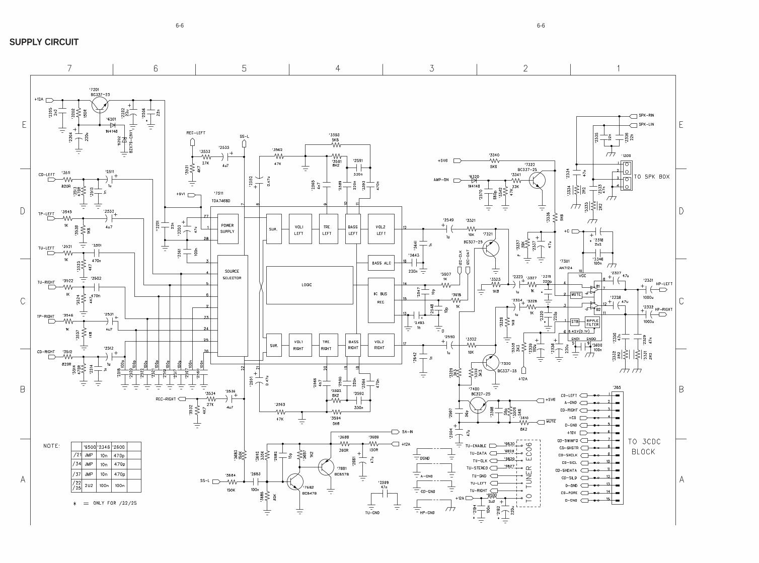
SUPPLY CIRCUIT
6-6 6-6
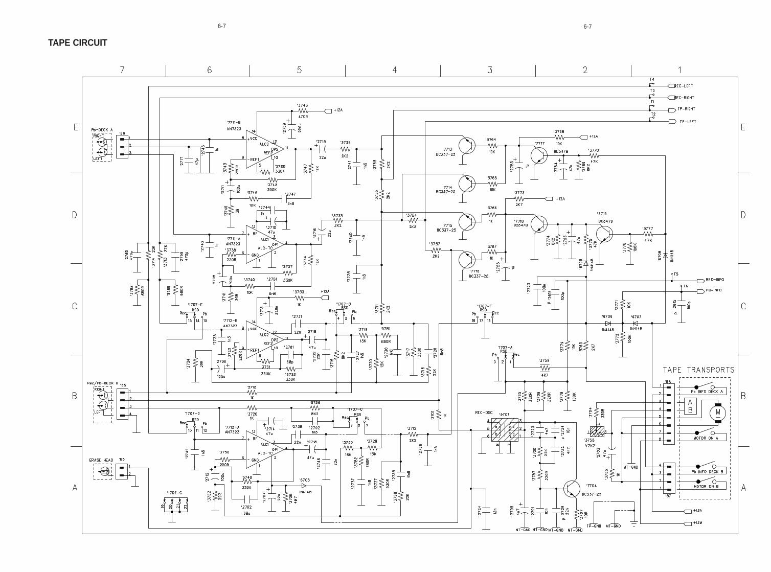
TAPE CIRCUIT
6-7 6-7
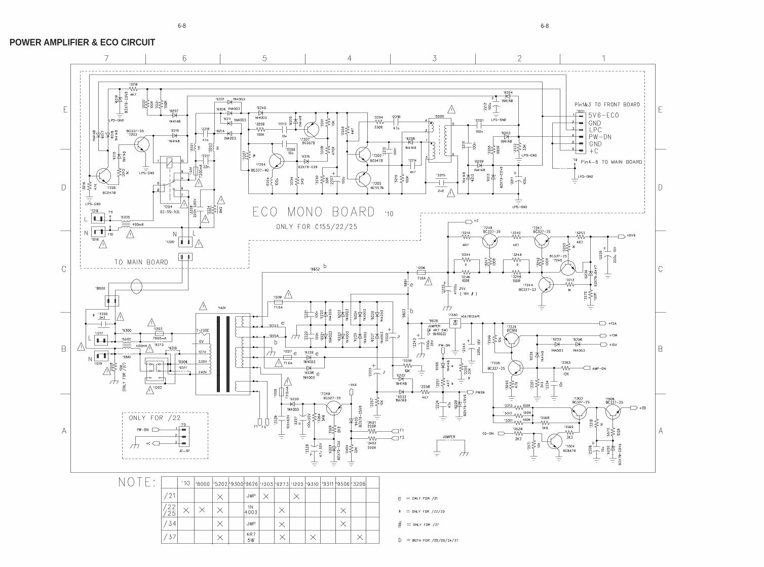
POWER AMPLIFIER & ECO CIRCUIT
6-8 6-8
6-96-9
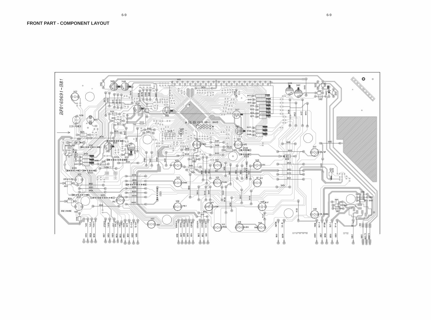
FRONT PART - COMPONENT LAYOUT
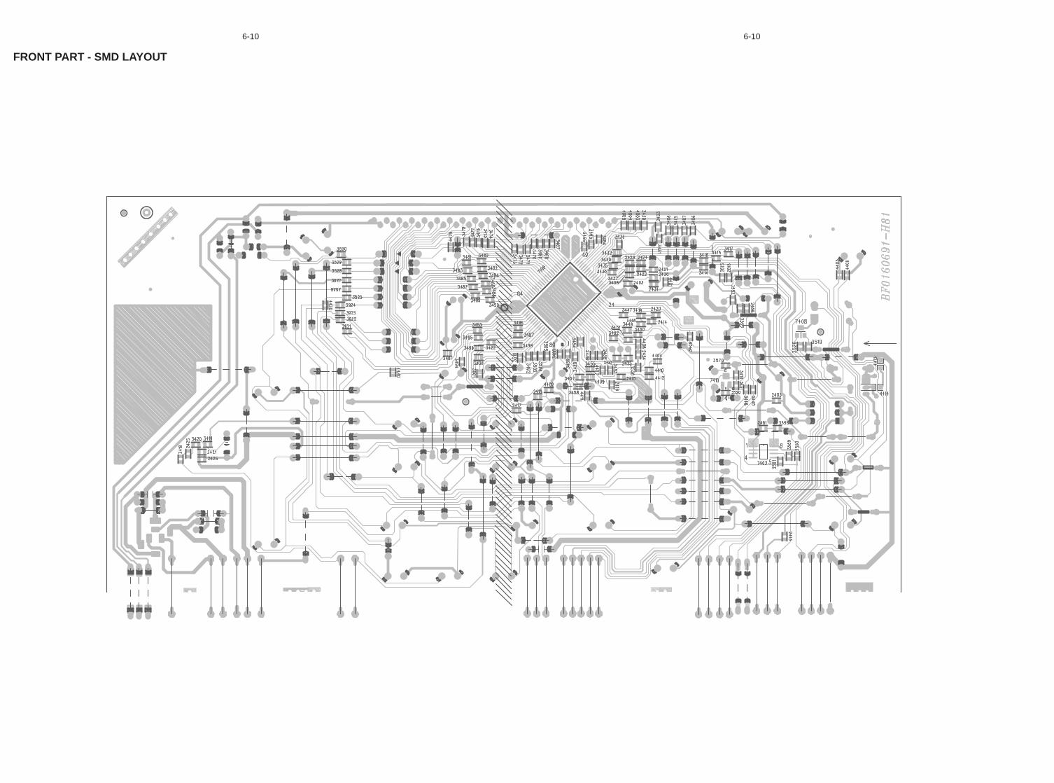
6-10 6-10
FRONT PART - SMD LAYOUT
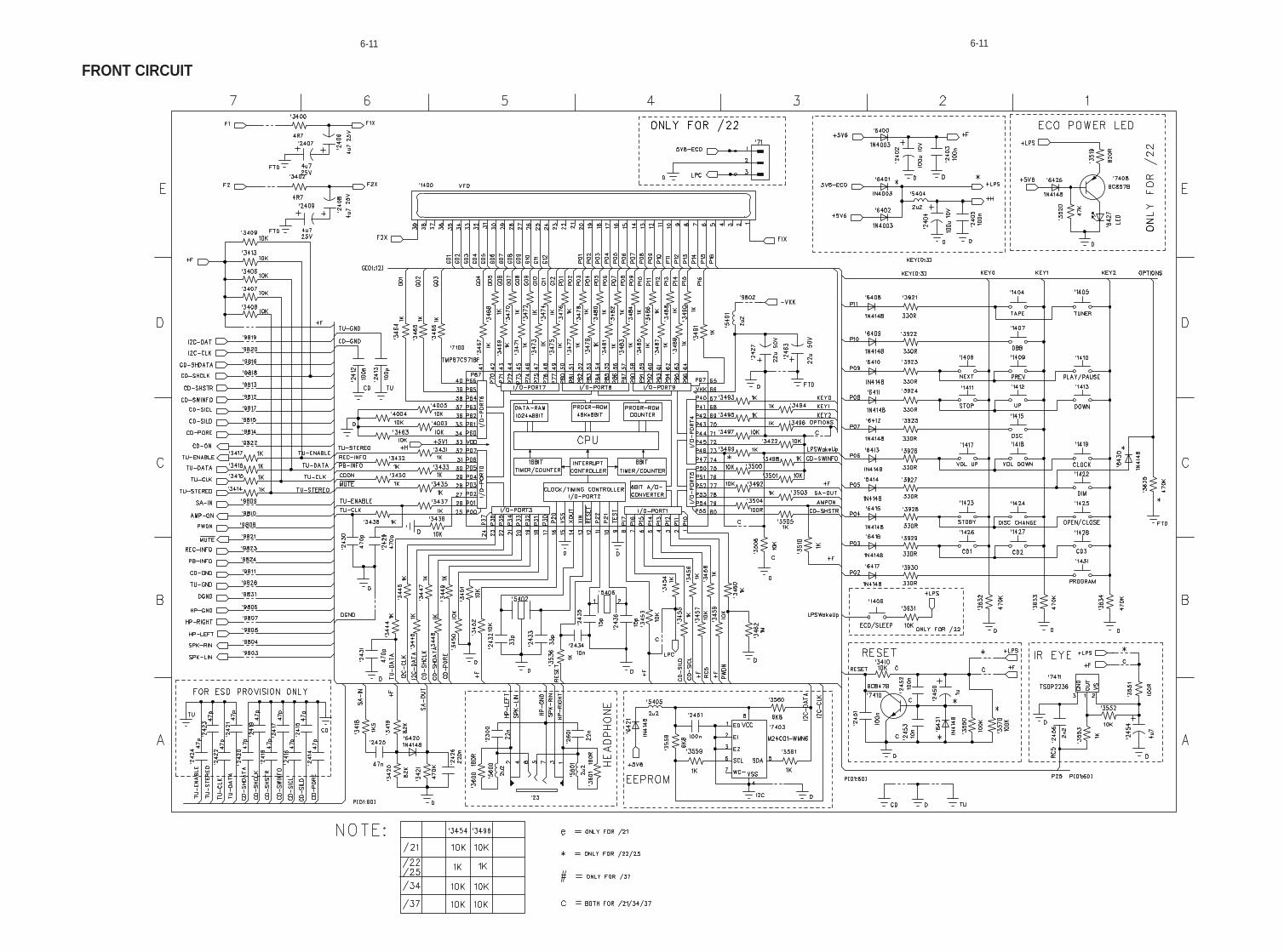
FRONT CIRCUIT
6-11 6-11
6-12 6-12
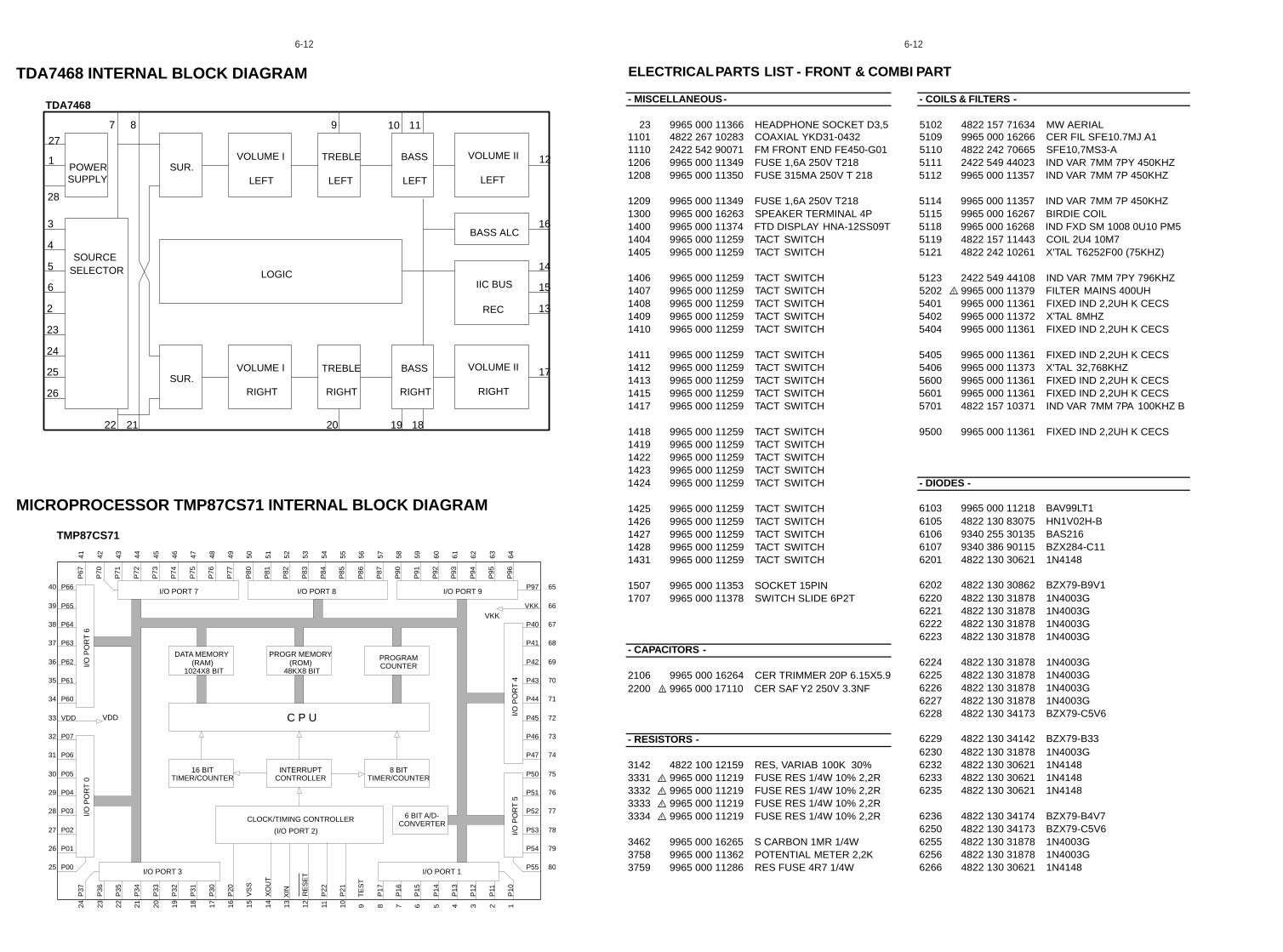
TDA7468 INTERNAL BLOCK DIAGRAM
VOLUME I
RIGHTSUR.
SOURCE
SUPPLYPOWER
SELECTOR
TREBLE
LEFT
VOLUME II
LOGIC
LEFT
REC
IIC BUS
BASS ALC
BASS
LEFT
VOLUME I
LEFTSUR.
TREBLE
RIGHT
VOLUME II
RIGHT
BASS
RIGHT
17
14
15
9
20
1
13
28
3
26
4
25
5
24
6
23
8
21
2
7
22
12
TDA7468
16
10
19
11
18
27
TMP87CS71
25 P00
26 P01
27 P02
28 P03
29 P04
30 P05
31 P06
32 P07
1P
10
2P
11
3P
12
4P
13
5P
14
6P
15
7P
16
8P
17
16P
20
10P
21
11P
22
17P
30
18P
31
19P
32
20P
33
21P
34
22P
35
23P
36
24P
37
67P40
68P41
69P42
70P43
71P44
72P45
73P46
74P47
75P50
76P51
77P52
78P53
79P54
80P55
34 P60
35 P61
36 P62
37 P63
38 P64
39 P65
40 P66
41P
67
42P
70
43P
71
44P
72
45P
73
46P
74
47P
75
48P
76
49P
77
50P
80
51P
81
52P
82
53P
83
54P
84
55P
85
56P
86
57P
87
58P
90
59P
91
60P
92
61P
93
62P
94
63P
95
64P
96
65P97
12R
ES
ET
9T
ES
T
33 VDD
66VKK
15V
SS
13X
IN
14X
OU
T
CLOCK/TIMING CONTROLLER
(I/O PORT 2)
C P U
I/O PORT 8
VDD
VKK
PROGR MEMORY(ROM)
48KX8 BIT
8 BITTIMER/COUNTER
16 BITTIMER/COUNTER
INTERRUPTCONTROLLER
6 BIT A/D-CONVERTER
I/O PORT 7 I/O PORT 9
I/O PORT 1
I/O P
OR
T 0
I/O P
OR
T 6
I/O P
OR
T 4
I/O P
OR
T 5
I/O PORT 3
DATA MEMORY(RAM)
1024X8 BIT
PROGRAMCOUNTER
MICROPROCESSOR TMP87CS71 INTERNAL BLOCK DIAGRAM
ELECTRICAL PARTS LIST - FRONT & COMBI PART
- MISCELLANEOUS - - COILS & FILTERS -
23 9965 000 11366 HEADPHONE SOCKET D3,5 5102 4822 157 71634 MW AERIAL1101 4822 267 10283 COAXIAL YKD31-0432 5109 9965 000 16266 CER FIL SFE10.7MJ A11110 2422 542 90071 FM FRONT END FE450-G01 5110 4822 242 70665 SFE10,7MS3-A1206 9965 000 11349 FUSE 1,6A 250V T218 5111 2422 549 44023 IND VAR 7MM 7PY 450KHZ1208 9965 000 11350 FUSE 315MA 250V T 218 5112 9965 000 11357 IND VAR 7MM 7P 450KHZ
1209 9965 000 11349 FUSE 1,6A 250V T218 5114 9965 000 11357 IND VAR 7MM 7P 450KHZ1300 9965 000 16263 SPEAKER TERMINAL 4P 5115 9965 000 16267 BIRDIE COIL1400 9965 000 11374 FTD DISPLAY HNA-12SS09T 5118 9965 000 16268 IND FXD SM 1008 0U10 PM51404 9965 000 11259 TACT SWITCH 5119 4822 157 11443 COIL 2U4 10M71405 9965 000 11259 TACT SWITCH 5121 4822 242 10261 X'TAL T6252F00 (75KHZ)
1406 9965 000 11259 TACT SWITCH 5123 2422 549 44108 IND VAR 7MM 7PY 796KHZ1407 9965 000 11259 TACT SWITCH 5202 9965 000 11379 FILTER MAINS 400UH1408 9965 000 11259 TACT SWITCH 5401 9965 000 11361 FIXED IND 2,2UH K CECS 1409 9965 000 11259 TACT SWITCH 5402 9965 000 11372 X'TAL 8MHZ1410 9965 000 11259 TACT SWITCH 5404 9965 000 11361 FIXED IND 2,2UH K CECS
1411 9965 000 11259 TACT SWITCH 5405 9965 000 11361 FIXED IND 2,2UH K CECS 1412 9965 000 11259 TACT SWITCH 5406 9965 000 11373 X'TAL 32,768KHZ1413 9965 000 11259 TACT SWITCH 5600 9965 000 11361 FIXED IND 2,2UH K CECS 1415 9965 000 11259 TACT SWITCH 5601 9965 000 11361 FIXED IND 2,2UH K CECS 1417 9965 000 11259 TACT SWITCH 5701 4822 157 10371 IND VAR 7MM 7PA 100KHZ B
1418 9965 000 11259 TACT SWITCH 9500 9965 000 11361 FIXED IND 2,2UH K CECS 1419 9965 000 11259 TACT SWITCH1422 9965 000 11259 TACT SWITCH1423 9965 000 11259 TACT SWITCH1424 9965 000 11259 TACT SWITCH - DIODES -
1425 9965 000 11259 TACT SWITCH6105 4822 130 83075 HN1V02H-B1426 9965 000 11259 TACT SWITCH6106 9340 255 30135 BAS2161427 9965 000 11259 TACT SWITCH6107 9340 386 90115 BZX284-C111428 9965 000 11259 TACT SWITCH6201 4822 130 30621 1N41481431 9965 000 11259 TACT SWITCH
6202 4822 130 30862 BZX79-B9V11507 9965 000 11353 SOCKET 15PIN6220 4822 130 31878 1N4003G1707 9965 000 11378 SWITCH SLIDE 6P2T6221 4822 130 31878 1N4003G6222 4822 130 31878 1N4003G6223 4822 130 31878 1N4003G
6224 4822 130 31878 1N4003G- CAPACITORS -
6225 4822 130 31878 1N4003G2106 9965 000 16264 CER TRIMMER 20P 6.15X5.9 6226 4822 130 31878 1N4003G
6227 4822 130 31878 1N4003G6228 4822 130 34173 BZX79-C5V6
6229 4822 130 34142 BZX79-B33- RESISTORS -6230 4822 130 31878 1N4003G
3142 4822 100 12159 RES, VARIAB 100K 30% 6232 4822 130 30621 1N41483331 9965 000 11219 FUSE RES 1/4W 10% 2,2R 6233 4822 130 30621 1N41483332 9965 000 11219 FUSE RES 1/4W 10% 2,2R 6235 4822 130 30621 1N41483333 9965 000 11219 FUSE RES 1/4W 10% 2,2R
6236 4822 130 34174 BZX79-B4V73334 9965 000 11219 FUSE RES 1/4W 10% 2,2R 6250 4822 130 34173 BZX79-C5V6
3462 9965 000 16265 S CARBON 1MR 1/4W 6255 4822 130 31878 1N4003G3758 9965 000 11362 POTENTIAL METER 2,2K 6256 4822 130 31878 1N4003G3759 9965 000 11286 RES FUSE 4R7 1/4W 6266 1N4148
!
!
!
!
!
4822 130 30621
2200 9965 000 17110 CER SAF Y2 250V 3.3NF!
6103 9965 000 11218 BAV99LT1
6-13 6-13
ELECTRICAL PARTS LIST
- DIODES - - IC & TRANSISTORS -
6320 4822 130 30621 1N41486400 4822 130 31878 1N4003G6401 4822 130 31878 1N4003G6402 4822 130 31878 1N4003G6403 4822 130 34173 BZX79-C5V6
7408 4822 130 60373 BC856B
6408 4822 130 30621 1N4148
7410 5322 130 60159 BC846B
6409 4822 130 30621 1N4148
7411 9965 000 11375 SENSOR RECEIVER
6410 4822 130 30621 1N4148
7504 5322 130 60159 BC846B
6411 4822 130 30621 1N4148
7506 4822 130 40981 BC337-25
6412 4822 130 30621 1N4148
7511 9322 150 74668 IC SM TDA7468D (ST00) R
6413 4822 130 30621 1N4148
7681 4822 130 60373 BC856B
6414 4822 130 30621 1N4148
7682 5322 130 60159 BC846B
6415 4822 130 30621 1N4148
7704 4822 130 40981 BC337-25
6416 4822 130 30621 1N4148
7711 4822 209 17498 AN7323
6417 4822 130 30621 1N4148
7712 4822 209 17498 AN7323
6420 4822 130 30621 1N4148
7713 4822 130 40981 BC337-25
6421 4822 130 30621 1N4148
7714 4822 130 40981 BC337-25
6426 4822 130 30621 1N4148
7715 4822 130 40981 BC337-25
6427 9322 179 76676 LED VS LTL-816EELC
7716 4822 130 40981 BC337-25
6430 4822 130 30621 1N4148
7717 4822 130 40959 BC547B7718 4822 130 40959 BC547B7719 4822 130 40959 BC547B
6703 4822 130 30621 1N41486706 4822 130 30621 1N41486707 4822 130 30621 1N41486708 4822 130 30621 1N4148
6709 4822 130 30621 1N41489626 4822 130 31878 1N4003G
- IC & TRANSISTORS -
7100 3139 110 53480 TMP87CS71BF7101 9351 772 20557 IC SM TEA5762H/V1 7110 4822 130 60373 BC856B7111 5322 130 42755 BC847C7112 4822 130 40959 BC547B
7201 4822 130 40981 BC337-257234 5322 130 44593 BC3697235 4822 130 40981 BC337-257244 4822 130 40981 BC337-257245 4822 130 40981 BC337-25
Note : Only these parts mentioned in the list are
7247 4822 130 40981 BC337-25
normal service parts.
7248 4822 130 40981 BC337-257249 4822 130 41246 BC327-257250 9965 000 11394 IC KIA7812API7301 4822 209 12925 AN7124
7320 BC337-257321 4822 130 40981 BC337-257322 4822 130 40981 BC337-257400 4822 130 41246 BC327-25
- IC & TRANSISTORS -
9630 4822 157 11477 FIXED IND. 2.2µH
6431 4822 130 30621 1N4148
7403 9965 000 04931 M24C01-WMN6
4822 130 40981

7-1
ECO POWER BOARD
TABLE OF CONTENTS
ECO Power Circuit ................................................................... 11-2
ECO Power Layout ................................................................... 11-3
Electrical Parts List ................................................................... 11-4
7-1
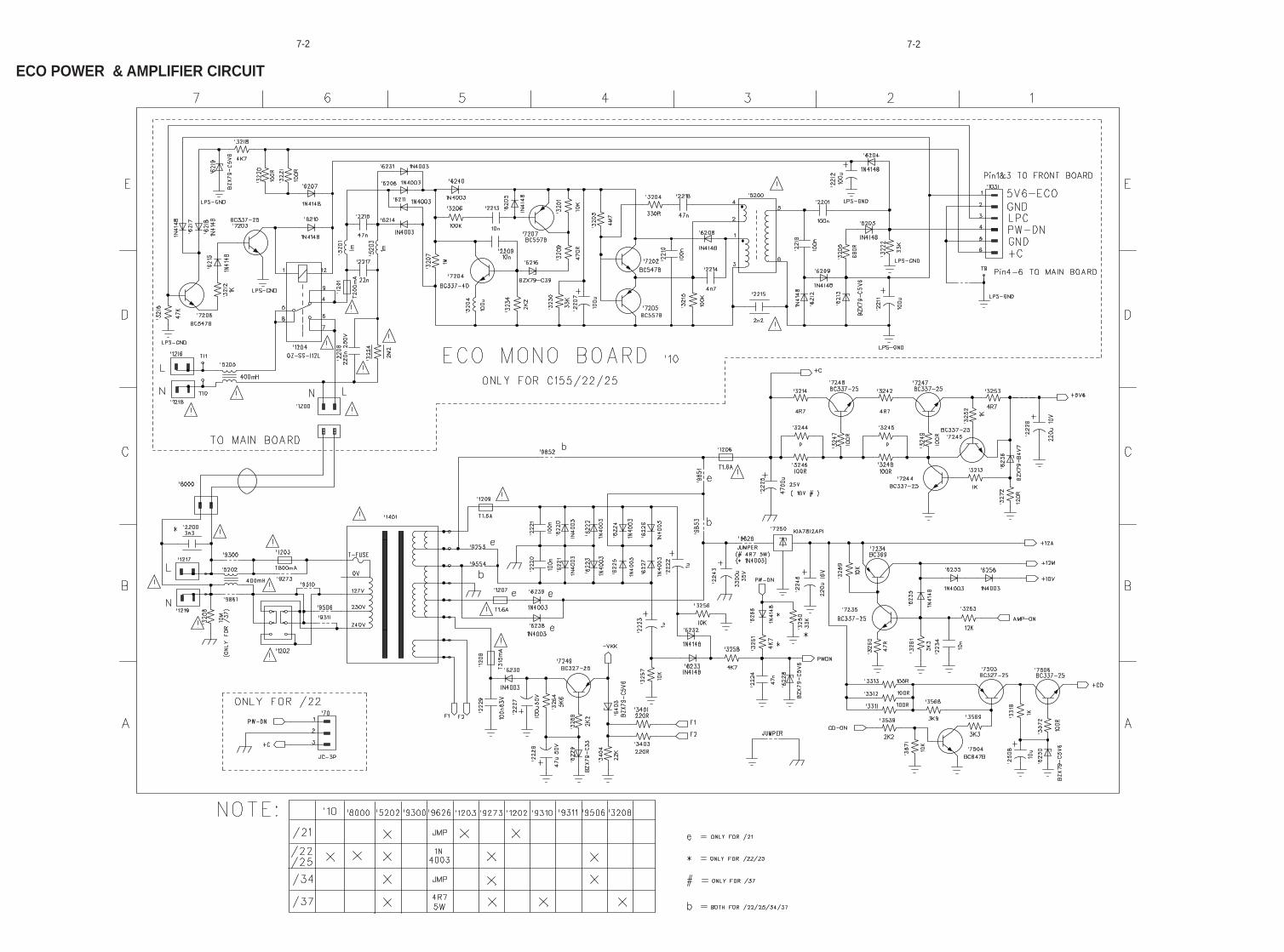
ECO POWER & AMPLIFIER CIRCUIT
7-2 7-2
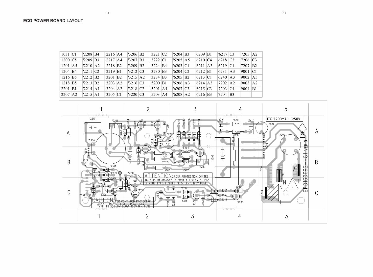
ECO POWER BOARD LAYOUT
7-3 7-3
'1031 C1 '2208 B4 '2216 A4 '3206 B2 '3221 C2 '5204 B3 '6209 B1 '6217 C3 7205 A2
'1200 C5 '2209 B3 '2217 A4 '3207 B3 '3222 C1 '5205 A5 '6210 C4 6218 C3 7206 C3
'1201 A5 '2210 A2 '2218 B2 '3209 B2 '3224 B4 '6203 C1 '6211 A3 6219 C1 7207 B2
'1204 B4 '2211 C2 '2219 B1 '3212 C3 '3230 B3 '6204 C2 '6212 B1 6231 A3 9001 C1
'1216 B5 '2212 B2 '3201 B2 '3215 A2 '3234 B3 '6205 B2 '6213 C1 6240 A3 9002 A5
'1218 B5 '2213 B2 '3203 A2 '3216 C3 '5200 B1 '6206 A3 '6214 A3 7202 A2 9003 A2
'2201 B1 '2214 A1 '3204 A2 '3218 C2 '5201 A4 '6207 C3 '6215 C3 7203 C4 9004 B1
'2207 A2 '2215 A1 '3205 C1 '3220 C3 '5203 A4 '6208 A2 '6216 B3 7204 B3
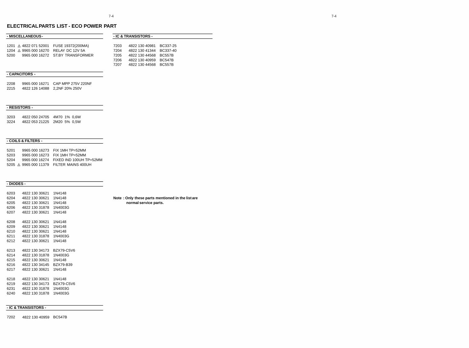
7-4 7-4
ELECTRICAL PARTS LIST - ECO POWER PART
- MISCELLANEOUS - - IC & TRANSISTORS -
1201 4822 071 52001 FUSE 19372(200MA) 7203 4822 130 40981 BC337-251204 9965 000 16270 RELAY DC 12V 5A 7204 4822 130 41344 BC337-405200 9965 000 16272 ST.BY TRANSFORMER 7205 4822 130 44568 BC557B
7206 4822 130 40959 BC547B7207 4822 130 44568 BC557B
- CAPACITORS -
2208 9965 000 16271 CAP MPP 275V 220NF2215 4822 126 14088 2,2NF 20% 250V
- RESISTORS -
3203 4822 050 24705 4M70 1% 0,6W3224 4822 053 21225 2M20 5% 0,5W
- COILS & FILTERS -
5201 9965 000 16273 FIX 1MH TP=52MM5203 9965 000 16273 FIX 1MH TP=52MM5204 9965 000 16274 FIXED IND 100UH TP=52MM5205 9965 000 11379 FILTER MAINS 400UH
- DIODES -
6203 4822 130 30621 1N41486204 4822 130 30621 1N4148 Note : Only these parts mentioned in the list are6205 4822 130 30621 1N4148 normal service parts.6206 4822 130 31878 1N4003G6207 4822 130 30621 1N4148
6208 4822 130 30621 1N41486209 4822 130 30621 1N41486210 4822 130 30621 1N41486211 4822 130 31878 1N4003G6212 4822 130 30621 1N4148
6213 4822 130 34173 BZX79-C5V66214 4822 130 31878 1N4003G6215 4822 130 30621 1N41486216 4822 130 34145 BZX79-B396217 4822 130 30621 1N4148
6218 4822 130 30621 1N41486219 4822 130 34173 BZX79-C5V66231 4822 130 31878 1N4003G6240 4822 130 31878 1N4003G
- IC & TRANSISTORS -
7202 BC547B
!
!
!
4822 130 40959
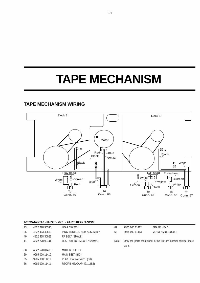
9-1
TAPE MECHANISM
RedScreen
WhiteYellow
Screen
White
R/P head Erase headPlay head
Red
White Screen
White
Black
Black
Blue
Blue
White
RedBlack
Motor
Deck 2 Deck 1
ToConn. 67
ToConn. 68
ToConn. 66
ToConn. 65
ToConn. 69
TAPE MECHANISM WIRING
MECHANICAL PARTS LIST - TAPE MECHANISM
23 4822 278 90596 LEAF SWITCH
35 4822 403 40513 PINCH ROLLER ARM ASSEMBLY
40 4822 358 30921 RF BELT (SMALL)
41 4822 278 90744 LEAF SWITCH MSW-17820MVD
58 4822 528 81415 MOTOR PULLEY
59 9965 000 11410 MAIN BELT (BIG)
65 9965 000 11411 PLAY HEAD AP-4211L(S3)
66 9965 000 11411 REC/PB HEAD AP-4211L(S3)
67 9965 000 11412 ERASE HEAD
68 9965 000 11413 MOTOR M9T12U20-T
Note: Only the parts mentioned in this list are normal service spare
parts.
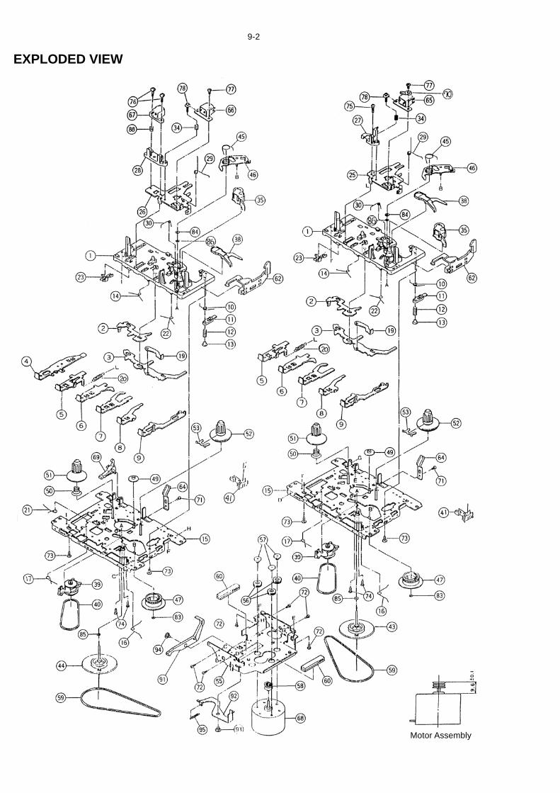
9-2
EXPLODED VIEW
Motor Assembly
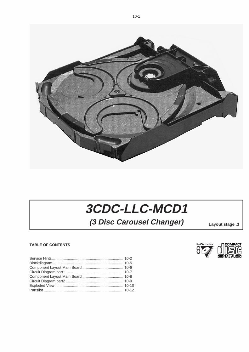
10-1
TABLE OF CONTENTS
Service Hints .....................................................................10-2Blockdiagram ....................................................................10-5Component Layout Main Board ........................................10-6Circuit Diagram part1 ........................................................10-7Component Layout Main Board ........................................10-8Circuit Diagram part2 ........................................................10-9Exploded View ..................................................................10-10Partslist .............................................................................10-12
3CDC-LLC-MCD1(3 Disc Carousel Changer) Layout stage .3
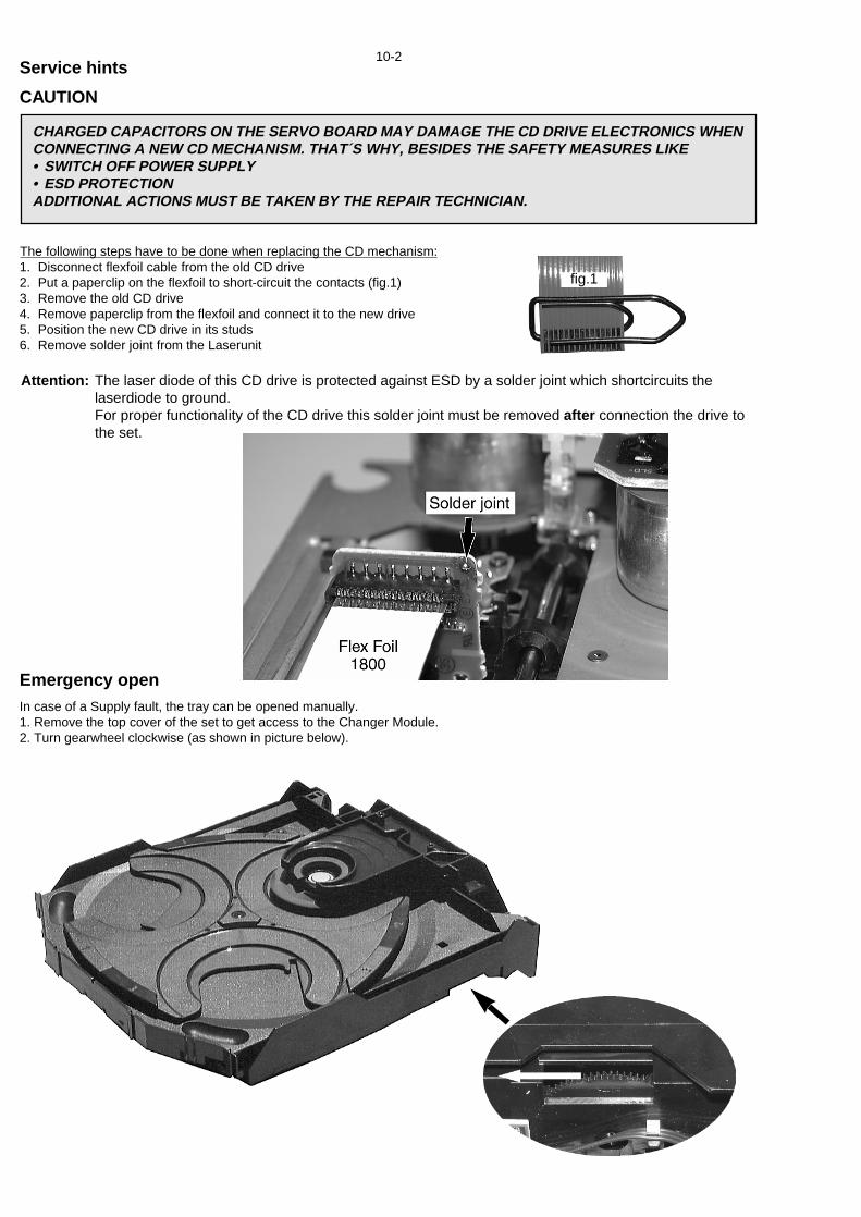
10-2
The following steps have to be done when replacing the CD mechanism:1. Disconnect flexfoil cable from the old CD drive2. Put a paperclip on the flexfoil to short-circuit the contacts (fig.1)3. Remove the old CD drive4. Remove paperclip from the flexfoil and connect it to the new drive 5. Position the new CD drive in its studs6. Remove solder joint from the Laserunit
CHARGED CAPACITORS ON THE SERVO BOARD MAY DAMAGE THE CD DRIVE ELECTRONICS WHENCONNECTING A NEW CD MECHANISM. THAT´S WHY, BESIDES THE SAFETY MEASURES LIKE• SWITCH OFF POWER SUPPLY• ESD PROTECTIONADDITIONAL ACTIONS MUST BE TAKEN BY THE REPAIR TECHNICIAN.
fig.1
Attention: The laser diode of this CD drive is protected against ESD by a solder joint which shortcircuits thelaserdiode to ground.For proper functionality of the CD drive this solder joint must be removed after connection the drive tothe set.
Emergency open
Service hints
In case of a Supply fault, the tray can be opened manually.1. Remove the top cover of the set to get access to the Changer Module.2. Turn gearwheel clockwise (as shown in picture below).
CAUTION
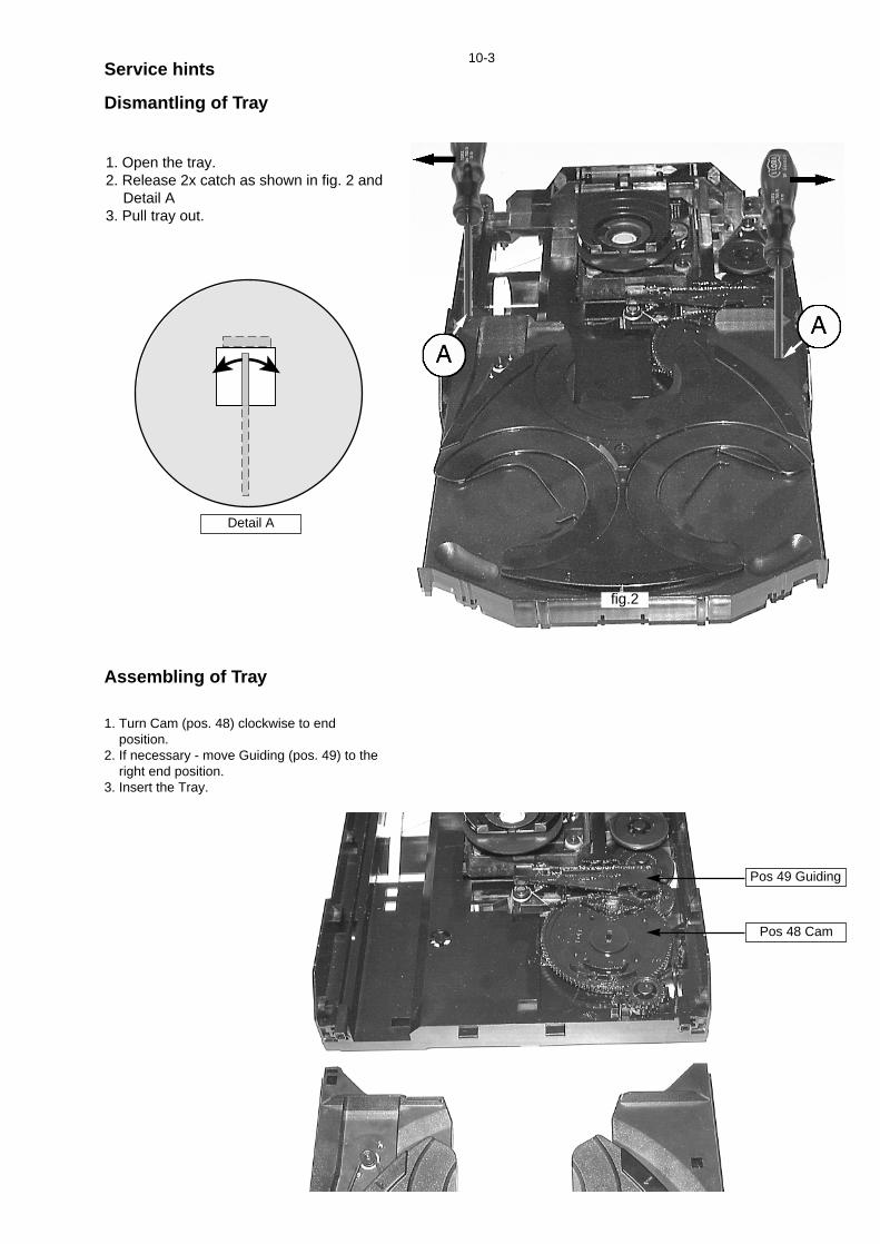
10-3
Pos 49 Guiding
Pos 48 Cam
Detail A
Dismantling of Tray
Service hints
1. Open the tray.2. Release 2x catch as shown in fig. 2 and
Detail A3. Pull tray out.
fig.2
Assembling of Tray
1. Turn Cam (pos. 48) clockwise to endposition.
2. If necessary - move Guiding (pos. 49) to theright end position.
3. Insert the Tray.
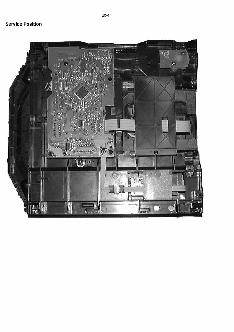
10-4
Service Position
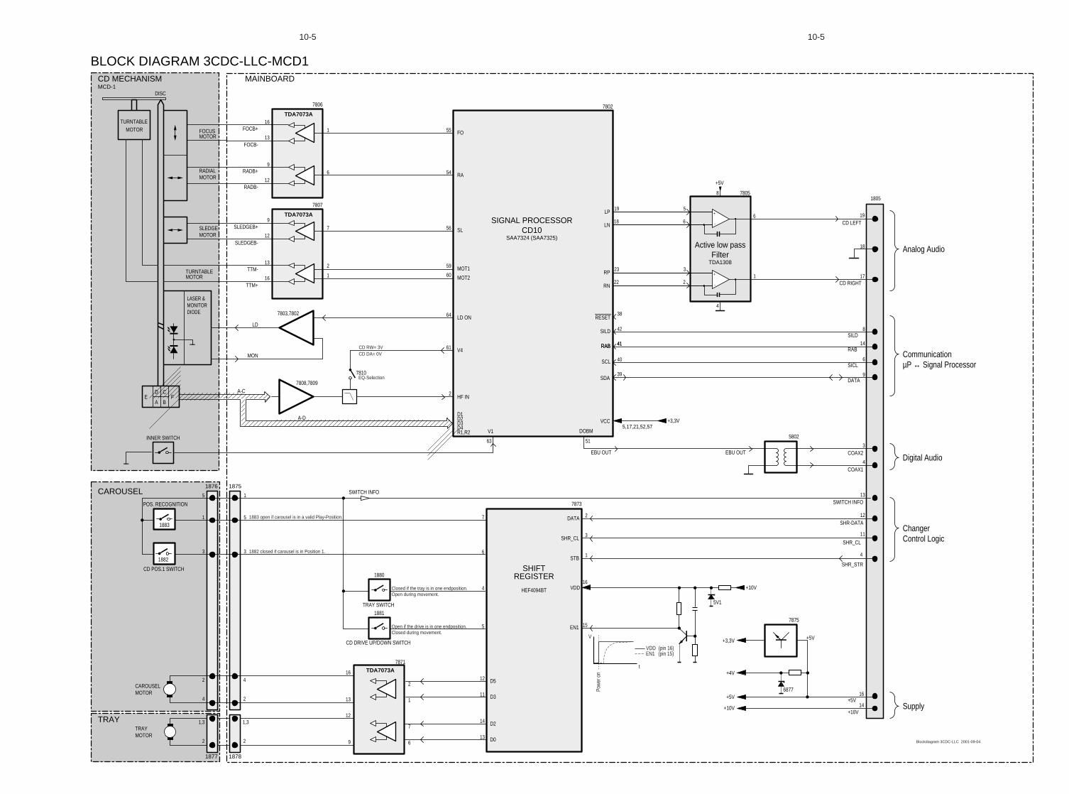
10-510-5
SDA
VCC
DOBM
A-D
A-C
7871
1876 1875
1877 1878
7873
HEF4094BT
LD ON
HF IN
V1
D1D2D3D4R1,R2
MOT1
REGISTERSHIFT
SIGNAL PROCESSORCD10
SAA7324 (SAA7325)
TRAYMOTOR
CAROUSELMOTOR
SL
D5
VDD
D3
D2
D0
RA
FO
DIODESPHOTO
FE
INNER SWITCH
SWITCH INFO
LASER &MONITORDIODE
TURNTABLEMOTOR
DISC
CD MECHANISM
CAROUSEL
TRAY
MAINBOARD
DATA
SHR_CL
7802
38
42
40
39
5,17,21,52,57
64
V461
2
63 51
2
3
STB 1
12
11
16
13
9
121,3
2
2
4
1,3
2
4
2
3
5
1
3
1
5
14
13
2
1
7
6
+3,3V
SCL
SILD
RESET
Blockdiagram 3CDC-LLC 2001-09-04
+5V
+4V
+3,3V
+10V
7875
+5V
6877
BLOCK DIAGRAM 3CDC-LLC-MCD1
+10V
15
16
5V1
V
t
EN1
CD DRIVE UP/DOWN SWITCH
1881
1880
TRAY SWITCH
1882
CD POS.1 SWITCH
POS. RECOGNITION
6
7
4
5
1882 closed if carousel is in Position 1.
18831883 open if carousel is in a valid Play-Position.
CD RW= 3VCD DA= 0V
EQ-Selection
Closed if the tray is in one endposition.Open during movement.
Open if the drive is in one endposition.Closed during movement.
VDD (pin 16)EN1 (pin 15)
Pow
er o
n
FOCUSMOTOR
RADIALMOTOR
SLEDGEMOTOR
MOTORTURNTABLE
55
54
56
59
1
16
13
9
12
9
12
13
16
6
7
2
7806
TDA7073A
7807
7808,7809
7803,7802
7810
TDA7073A
TTM+
TTM-
LD
MON
SLEDGEB-
SLEDGEB+
RADB-
RADB+
FOCB-
FOCB+
MOT2601
BA
CD
EBU OUT
MCD-1
RAB 41
4
SHR_STR
TDA7073A
1805
17
18
19
14
16
13
3
4
11
SHR-DATA12
8
6
9
Active low passFilter
TDA1308
7805
12
3
6
56
+5V
8
4
+
-
+
-
CD LEFT
CD RIGHT22
23
18
19
RN
RP
LN
LP
DATA
SHR_CL
SWITCH INFO
COAX1
COAX2
14RAB
41RAB
EBU OUT
5802
SICL
SILD
+5V
+10VSupply
Digital Audio
ChangerControl Logic
Analog Audio
CommunicationµP ↔ Signal Processor
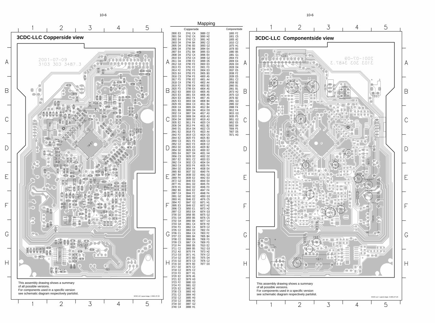
10-6 10-6
This assembly drawing shows a summaryof all possible versions.For components used in a specific versionsee schematic diagram respectively partslist.
3CDC-LLC Layout stage .3 2001-07-25
3CDC-LLC Componentside view
This assembly drawing shows a summaryof all possible versions.For components used in a specific versionsee schematic diagram respectively partslist.
3CDC-LlC Layout stage .3 2001-07-25
3CDC-LLC Copperside view2800 E32801 D42802 E42803 D42805 D42806 D42807 E42808 D42810 E42811 D42812 G32813 F32814 F22815 E42816 C32817 F32818 C42819 F22820 F32822 E32823 E32824 E32825 E32829 H32830 C42831 B32832 C42833 C42834 D42835 E22836 D42840 D12841 E22842 F22844 E22850 C32852 C22853 D22854 D22855 E42856 C32857 E22862 C42863 C42864 D22865 B32867 B42869 F42872 G22877 H12878 H12882 B32887 C42891 G22893 H12894 F22895 E32896 C32897 C23700 D23701 G43702 G43703 G43704 F33705 C23706 C13707 C23708 C23709 C33710 F43711 C23712 A33713 G33714 G23715 G23716 D23717 D23718 C23719 F33720 E23721 E23723 F23724 F23725 E23730 C33731 C23732 C23733 C23734 D23740 C4
3741 C43742 C43743 C33744 B43746 B33750 B43751 B43752 C43753 C43789 F23790 F33791 F23792 F33793 F33794 F33795 E23796 F23798 E43799 E43800 E33801 E43802 F43803 D43804 C33805 D43806 D43807 D43808 D43809 D23811 F43813 F43814 D43818 F33819 C33820 F33821 F33822 F33825 E33826 E33827 D43828 D23831 C23832 C33833 F43834 F43837 D23838 D23839 E23840 E33841 D23842 D23843 E23844 F23845 D23846 E23847 G23849 E23850 E13853 E43858 B53859 B53860 B43861 C43862 C43863 D23864 C43865 B43866 B53867 C43868 B53869 B53870 F43871 H13872 B33873 C33874 B33875 C23876 C23877 H13878 A53879 H33880 G33881 G23882 H23883 H33884 H33885 H33886 H23887 G23888 H1
3889 C23890 H23891 H23892 C23893 G23894 E43895 E33896 E43898 G23899 D53900 E33901 F33904 E33905 B34800 A54801 A44802 A44803 B24804 A54805 A54806 A54807 A54808 B44811 B44812 B44814 D34817 A34818 A34819 A34820 C44821 B24822 C54823 A44824 C54825 B34826 C34828 C24829 B24830 E24831 H44832 D24833 E34834 E44835 F44838 E44840 F44841 G24842 E34844 E44845 F44846 F34847 F44848 F44850 G34876 C56871 H16872 H26873 H26874 G36875 G26876 C56877 C46878 H26879 C27802 F47803 F27805 B47808 F37809 F37810 E27812 G37873 H27874 C27875 D47876 C27877 D3
1800 F21801 C51805 A21810 C21875 H11878 B31880 B51881 G12804 F32809 E42826 D32828 D42837 E52838 F22839 E52851 C22858 B22860 B12861 B12873 H22875 G32876 B22881 G32885 D22888 F43812 F43815 G33835 F53851 G23852 E55802 B47806 F57807 D57871 H3
MappingCopperside Componentside
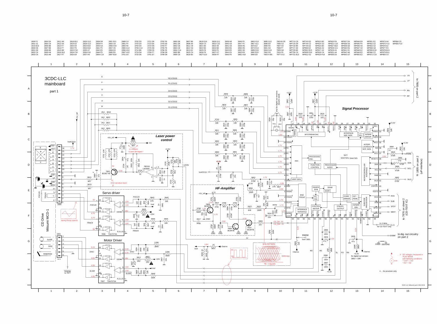
10-710-7
+
-
+
-
VDDINTERFACEVERSATILE
DEMODEFM
PLLDIG.
STAGESOUTPUT
CONTROLMOTOR
KILL
INTERF.LOOPBACKSER. DATA
INTERF.VERSAT.
INTERFACESER. DATABITSTREAM DACT
IMIN
G
INT
ER
FAC
EM
ICR
OC
ON
TR
OLL
ERPROCESSOR
AUDIO
PROCESSING
PRE-
FUNCTIONCONTROL
SRAM
ADDR
INTERF.EBU
DET.PEAK
CORR.ERROR
PR
OC
ES
SO
RS
UB
CO
DE
ENDFRONT
VREF GEN.
ADC
+
-
+
-
VDD
MP847 H2MP848 E2MP849 E2MP850 E2
MP851 E2MP852 G2MP853 G2
120K
LDON
+
MP730 C9
TR
AC
K
C
FOCUS
on78
76
1V
F
(CD
-TE
XT
IC)
4.7V
MP841 F6MP842 H6MP843 G7
MP844 E9MP845 F4MP846 H2
3789 F83790 F73791 E7
3792 F8
+
Servo driver
_Motor Driver
+
2851 B11
_
7808 F77809 G87810 F97877 D12
MP713 C9MP715 D9MP716 B9MP717 A9MP729 B9
3842 E63843 E53844 E5
(uP
-inte
rfac
e)
B
to
180K
TRACK
3798 D8
11.3 MHz
CD
Driv
e
control
to 7805 on part 2
3704 D43709 C143710 B83719 D43720 D5
3721 D63723 E63724 D63725 D6
2838 D82839 F4
3863 = 33R
part
2
2802 C8
B
SLIDE
_
D
A
2801 D8
E
2840 G42841 F52842 E52844 F52850 C14
3828 G113832 C153833 A83834 B83835 F53837 G73838 H7
3839 H63840 G53841 G5
E
R1 (CD10)
from 1801
on
2820 D4
_
C
Laser power
2816 B122817 F7
2818 B113793 E83794 F73795 F83796 F8
2822 F92823 F102824 F102825 E9
2826 G122828 G132833 B102834 B102835 H72836 E102837 H4
1 2 3 4 5 6
1810 B102800 D8
2855 C82856 D152857 H52869 D32885 E92887 B10
2888 C42891 F42894 F82895 G122896 H122897 H123701 D3
E
+
MON
VREF
D
only
for
digi
tal o
ut v
ersi
ons
D
E
F
G
H
A
B
2819 E5
D
E
F
G
H
1800 F11801 G1
TRACK
SLIDE
D4 (CD10)
7 8 9 10 11 12 13 14 15
2 3 4 5 6 7 8
INNERSW.
D3 (CD10)
PIN50DISC
to
dig. out circuitry
#.... for provision only
T+
A
(Qua
rtz
used
)
DISC DISC
F
1805
for digital out version:
F+
R2 (CD10)
C
10 11 12 13 14 15
A
SLIDE
B
C
/ SAA7325
D1 (CD10)
on
mainboard
GND
3CDC-LLC
_
D
F-
part 1
B
#
+
FO
CU
S3702 D3
1
2803 C8
2804 D42805 C82806 B82807 B82808 B92809 H42810 A8
2811 A92812 D52813 F72814 F72815 B8
GND
LD
for CD TEXT only
to
shee
t 2
7803-B D57806 G37807 H3
3815 C43818 B3
3819 D143820 C33821 B33822 B33825 F93826 F9
9
3799 D8
3800 D83801 D83802 C83803 C83804 C143805 B83806 C8
3807 B93808 A93811 C83812 H43813 E2
_
FOCUS
MP818 C4MP819 F10
MP820 F8
VCC
3845 F6
3846 F53847 F53849 H53850 H53852 H53853 E93862 A10
3703 D3 3867 A113870 E23873 D143889 D153892 E153894 E9
3895 G123896 E93900 F93901 D43904 G107802 D37803-A B5
A
MP883 C4
MP884 C5MP893 F10
part 2
to 7877
120K
D2 (CD10)
MP821 C15MP827 B10MP828 G11MP829 A3MP831 A4MP836 D3
MP837 D4MP838 G6MP839 G6
3827 E10 MP731 B13
MP743 D2MP744 C2MP745 E2MP800 E2MP802 B15MP809 D10MP812 G2
MP813 B3MP814 G2MP815 B3MP816 A3MP817 A3
Signal Processor
MP840 E6
T-
HF-Amplifier
DO
BM
F
C
#
3863 G13
+
MP858 G8MP859 E10MP860 C2MP872 C15
MP873 H4MP875 F13MP876 E2MP877 E3MP878 B13MP879 B11
39K
3721
47n
2835
470n
2894
100n
2820
2812
33p
2834
33p
GND GND
3704
1R
27p
2856
3800
2826
47u
3802
2K2
3795
10K
3803
33p
2833
2836 47
n
1810TF01
EBUGND
2807
2815
GND
GND
+3.3V
330K
3849
1K
3837
58
VS
SD
3
35WCLI
28
WC
LK
470R3873
63
V1
34V2|V3
61
V4
62
V5
5 VDDA1
17
VDDA2
52
VD
DD
1P
57
VD
DD
2C
20
VN
EG
21
VP
OS
7 VRIN
4 VSSA1
14 VSSA2
33VSSD1
50
VS
SD
2
RP
48SBSY
40SCL
37SCLI
29
SC
LK
39SDA
36SDI
24
SE
LPLL
47SFSY
42SILD
56
SL
43STATUS
46SUB
25
TE
ST
1
31
TE
ST
2
44TEST3
IREF
3 ISLICE
32KILL
64
LDON
18
LN
19
LP
59
MO
TO1
60
MO
TO2
12 R1
13 R2
54
RA
41RAB
45RCK
38RESETn
22
RN
23
49
CL11|4
26
CL1
6
16 CRIN
15 CROUT
8 D1
9 D2
10 D3
11 D4
27
DAT
A
51
DO
EM
30
EF
55
FO
2 HFIN
1 HFREF
6
5
6
7
8
4
SAA7324
7877
53
CF
LG
4K7
3870
7803-BLM358D
10K
4
8,11,15
8,11,15
3842
7806 TDA7073A
14
10
2
1
6
7
16
13
9
12
5
32822
1n2819
470R
3889
3834
10K
3832
220n
2809
+3servo
47R
4R7
3835
3701
2804
47u
+3.3V
3789
470R
220p
2805
2806
220p
3846
2816
1n5
47K
3811
3710
1n
BC847B7810
2841
2840
100n
2825
47R
3702
3820
1K38
38
2K2
1K 3798
BC847B7808
2855
2891
1n5
14
15
16
2
3
4
5
6
7
8
9
18001
10
11
12
13
2824
47R
3703
GND
3844
3806
10K
3K9
2800
2823
10K
+3.3V
3892
470R
2808
220p
3805
7
16
13
9
12
5
3
4
TDA7073A7807
14
10
2
1
6
2814
2802
3862
120R
1
2
3
4
5
6
3840
47u
2888
1801
PH-S
1K
3719
3801
10K
3853
470R
2839
47u
10n
3895
15R
+3servo
2857
3807
10K
10u
2838
2K7
3900
3894
100R
+10V
2801
220p
+3.3V
2850
1n
+3servo
3845
10K
1K 3799
+3.3V28
69
47n
2K2 3821
470R
3819
3863
100R
560R
3790
2828
47u
1n 2844
+3.3V
3796
3K3
1n5
2818
10K
3901
3812
2R2
3850
10K
470K
3720
2K2 3818
2813
82p
3826
120R
3867
3724
8K2
2817
560p
2842
1n5
10K
3841
3815
4R7
2811
220p
3808
10K
BC807-407802
4u7
+10V
2851
220u
2885
2K2 3822
5K6
3847
3K3
3792
2803
3791
220p
3813
4R7
3833
2K7
3723
100n
2897
100n
2895
100n
2896
3794
3852
2R2
3828
22K
BC847B7809
27K 3827
47K
3843
+5V
3725
47u
2837
3896
220K
100n
2887
3904
100K
3839
470R
3793
2810
3825
RN
RP
SBSY
SFSY
SL
SUB
Innersw
+5V_HF
+3.3V
+5V
_HF
CL11
DOBM
FO
LN
LP
M1M2RA
RCK
Vref
Innersw
Vref
+5V_HF
VrefCD10
+3.3V
VrefCD10
SILD
SICL
SDA
PORE
Vref
Vref HFIN
18K
18K
150p
330p22K
18K
18K
150p
150p
150p
22K
180p
820R
6n8
3n3
22n
470n
33K
390R
180R
+3.3V
10K
3804
150p
Mits
umi M
CD
-1
3CDC-LLC (Mitsumi) part1 2001 09 06
4.9V
10V
1.7V
1.7V
1.7V
1.7V
1.7V
1.7V
1.7V
3.3V
1.7V
3.2V
1.6V
1.6V
1.6V
3.4V
3.2V
4.8V
1.6V
1.6V
4.6V
3V3V 0V
4.7V
0.8V
10V
0.3V
1.7V
5.1V
1.6V
1.6V
5V
1.6V
3.2V
3.2V
1.6V
1.6V
1.6V
1.7V
5V
0.3V
1.6V
1.7V
1.6V
3.2V
4V
1.8V
1.2V
0.6V
2.4V
2.7V
4.7V
+3.3V
->Laser damaged !U >400mV
CD_RW : 3VCD_DA : 0V
0V
3V
800mVpp
EYE-PATTERN
TB = 0.5us/div
during Focus search
ESD sensitive lines!
. . . V DC voltages measured inPLAY MODEwith following conditions:"+10V" = 10V"+5V" = 5V
EVMV

10-8 10-8
This assembly drawing shows a summaryof all possible versions.For components used in a specific versionsee schematic diagram respectively partslist.
3CDC-LLC Layout stage .3 2001-07-25
3CDC-LLC Componentside view
This assembly drawing shows a summaryof all possible versions.For components used in a specific versionsee schematic diagram respectively partslist.
3CDC-LlC Layout stage .3 2001-07-25
3CDC-LLC Copperside view2800 E32801 D42802 E42803 D42805 D42806 D42807 E42808 D42810 E42811 D42812 G32813 F32814 F22815 E42816 C32817 F32818 C42819 F22820 F32822 E32823 E32824 E32825 E32829 H32830 C42831 B32832 C42833 C42834 D42835 E22836 D42840 D12841 E22842 F22844 E22850 C32852 C22853 D22854 D22855 E42856 C32857 E22862 C42863 C42864 D22865 B32867 B42869 F42872 G22877 H12878 H12882 B32887 C42891 G22893 H12894 F22895 E32896 C32897 C23700 D23701 G43702 G43703 G43704 F33705 C23706 C13707 C23708 C23709 C33710 F43711 C23712 A33713 G33714 G23715 G23716 D23717 D23718 C23719 F33720 E23721 E23723 F23724 F23725 E23730 C33731 C23732 C23733 C23734 D23740 C4
3741 C43742 C43743 C33744 B43746 B33750 B43751 B43752 C43753 C43789 F23790 F33791 F23792 F33793 F33794 F33795 E23796 F23798 E43799 E43800 E33801 E43802 F43803 D43804 C33805 D43806 D43807 D43808 D43809 D23811 F43813 F43814 D43818 F33819 C33820 F33821 F33822 F33825 E33826 E33827 D43828 D23831 C23832 C33833 F43834 F43837 D23838 D23839 E23840 E33841 D23842 D23843 E23844 F23845 D23846 E23847 G23849 E23850 E13853 E43858 B53859 B53860 B43861 C43862 C43863 D23864 C43865 B43866 B53867 C43868 B53869 B53870 F43871 H13872 B33873 C33874 B33875 C23876 C23877 H13878 A53879 H33880 G33881 G23882 H23883 H33884 H33885 H33886 H23887 G23888 H1
3889 C23890 H23891 H23892 C23893 G23894 E43895 E33896 E43898 G23899 D53900 E33901 F33904 E33905 B34800 A54801 A44802 A44803 B24804 A54805 A54806 A54807 A54808 B44811 B44812 B44814 D34817 A34818 A34819 A34820 C44821 B24822 C54823 A44824 C54825 B34826 C34828 C24829 B24830 E24831 H44832 D24833 E34834 E44835 F44838 E44840 F44841 G24842 E34844 E44845 F44846 F34847 F44848 F44850 G34876 C56871 H16872 H26873 H26874 G36875 G26876 C56877 C46878 H26879 C27802 F47803 F27805 B47808 F37809 F37810 E27812 G37873 H27874 C27875 D47876 C27877 D3
1800 F21801 C51805 A21810 C21875 H11878 B31880 B51881 G12804 F32809 E42826 D32828 D42837 E52838 F22839 E52851 C22858 B22860 B12861 B12873 H22875 G32876 B22881 G32885 D22888 F43812 F43815 G33835 F53851 G23852 E55802 B47806 F57807 D57871 H3
MappingCopperside Componentside
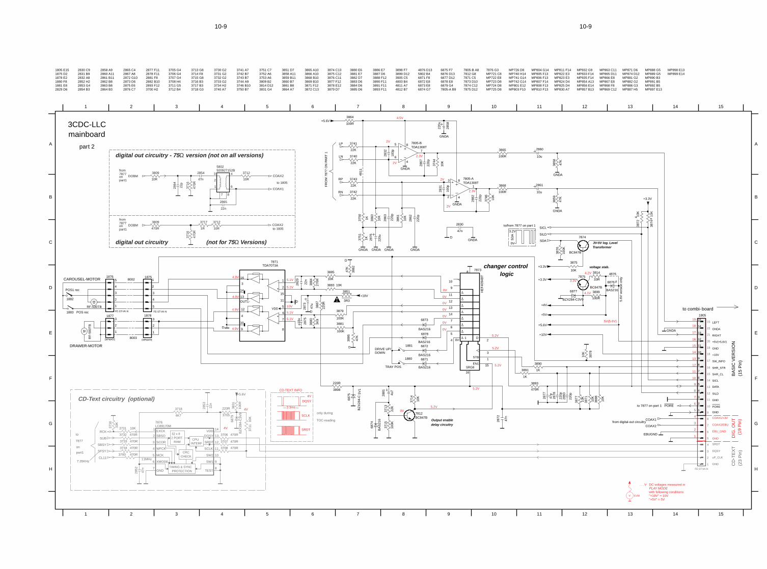
10-910-9
+
-
+
-
VDD
STB
D1
EN1SRG8
M
M
9 10 11 12
CAROUSEL-MOTOR
delay circuitry
PORE
C
D
E
F
voltage stab.
D
3
1 2 3 4 5 6 7 8 9 10 11 12 13 14 15
1 2 3 4 5 6 7 8
2873 D62875 E62876 C7
2877 F11
SILD
DRAWER-MOTOR
board
GND
SHR_STR
2 5.6V
ver
sion
onl
y
GNDA
13 14 15
A
B
C
D
E
F
G
H
A
B
3714 F83715 G83716 B33717 B3
1882
mainboard
(19
Pin
)
3CDC-LLC
D
D
1883
2852 H22853 G42854 B3
2858 A92860 A112861 B112862 B82863 B82864 B3
2865 C42867 A82872 G10
3750 B7
3751 C73752 A63753 A6
3V-5V log. Level
DIG
. OU
T
POS rec FE-ST-VK-N
LEFT
DIPMATE
1
from digital-out circuitry
SD
A
to 7877 on part 1
DOWN
1
2878 F112881 F82882 B102893 F123700 H2
3705 G43706 G43707 G43708 H43711 G53712 B4
3713 G8
3876 C113877 F123878 E123879 D7
3
RF
-500
TB
RF-500TB
1876
2
changer control
GND
COAX2/EBU
DRIVE UP/
3718 G3
3730 G23731 G23732 G23733 G23734 H23740 A7
3741 A73742 B73743 B73744 A93746 B10 MP724 D8
MP725 D8
MP726 D8MP740 H14
to/from 7877 on part 1
D
3809 B23814 D123831 G4
3851 D73858 A113859 B113860 B73861 B83864 A7
3865 A103866 A103868 B103869 B103871 F123872 C13
3874 C133875 C12
MP811 F14MP822 E3MP823 E3MP824 D4
BA
SIC
VE
RS
ION
COAX1/+3V
6871 F86872 E86873 E86874 G7
6875 F76876 D136877 D126878 E86879 G47805-A B9
7805-B A87812 G87871 C57873 D107874 C127875 D12
7876 G3MP721 C8MP722 E8MP723 D8
MP886 G3MP887 H5
MP888 G5MP889 G5
FR
OM
787
7 O
N P
AR
T 1
SHR_CL
3.2V
SICL
5V1
MP741 G14MP742 G14MP801 E12MP803 F10
MP804 G14MP805 F13MP806 F13MP807 F14MP808 F13MP810 F13
4803 B44811 A74812 B7
4876 D135802 B4
+5V(+5.6V)
DATA
GND
MP825 D4MP830 A7
MP832 G9MP833 F14MP835 F14MP854 A13MP856 E14MP857 B13
MP863 C11MP865 D11MP866 E8MP867 E8MP868 F8MP869 C12
MP871 D6MP874 D12MP881 G2MP882 G2
EBU_GND
5
8003
Transformer
1877
#
#
#
3880 E63881 E73882 D73883 D63884 D63885 D6
3886 E73887 D63888 F123890 F113891 F113893 F11
3898 F73899 D123905 C5
4
D
logic
(15
Pin
)
0V
G
H
1805 E151875 D21878 E21880 F81881 E82829 D6
2830 C92831 B92832 A8
Output enable
+10V
GND
part 2
MP890 B3MP891 B5MP892 B5MP897 E13
MP898 E13MP899 E14
0V
to combi-
D
TRAY POS
8002
SW_INFO
POS1 rec
RIGHT
EBUGND
2860
10u
2878
220p
3874
10K
3858
47K
1K
3891
BAS216
6876
1880
10K
3878
9
125
3
4
8
11
15
7871TDA7073A
14
10
2
1
6
7
16
13
OUT1-
220R
3898
1
2
3
4
5
GNDA
1875
FE-ST-VK-N
220R
3887
47p
2877
3744
10K
3741
22K
7875
BC847B3899
100R3R3
3851
4811
3872
10K
2867
220p
3746
10K
3860
220p
2862
3715
100K
10K
22K
3713
3879
100K
2858
220u
470R
3893
10K
3714
3742
22K
220p
2893
BC847B7812
8
4
TDA1308T7805-A3
2
1
BAS216
6871
1K3750
13
12
11
9
10
1
16
8
HE
F40
94B
T
7873
3
2
15
4
5
6
7
14
10K
3877
2863
220p
10u
GNDA
3875
10K
2875
6874
BA
S21
6
BZX284-C3V9
6877
33R
3814 4876
3740
22K
BZ
X28
4-C
6875
2872
47n
2861
10u100R
3868
100R
3865
3864
100R
GNDA
22n
2829
3884
270R
3859
47K
31878
DIPMATE
1
2
2831
100p
3876
100K
3883 10K
1881
BAS216
6873
GNDA
47K
3880
3K9
3882
3885
10K
GNDA
7874
BC847B
GNDA
3861
10K
10K
3871
BAS216
6872
100K
3881
10K
3888
3886
47K
3751
1K
2873
4u7
2881
47u
3743
22K
2882
220p
TDA1308T5
6
7
8
4
7805-B
6
7
8
9
17
18
19
2
20
21
22
23
3
4
5
1
10
11
12
13
14
156
7
8
9
2
3
4
5
1
10
11
12
13
14
15
16
6
7
8
9
17
18
19
2
3
4
5
1
10
11
12
13
14
15
16
1805
6878
BAS216
GNDA
GNDA
2832
100p
GNDA
GNDA
47n
2830
3890
1K28
76
220u
GNDA
COAX1
+5.6V
+3.3V
+3.3V
+5V
RN
RP
LN
LP
COAX2
+4V
+5.6V
+10V
+3.3V
+10V
SICL
SDA
PORE
SILD
CD
-TE
XT
GND
DQSY
(23
Pin
)
uP_CLK
SRDT
FE-ST-VK-NPROTECTION
TIMING & SYNC
CHECKCRC
INTERFCPU
RAM2 PORT32 x 8
only during
11MHz
TOC-reading
DQSY
3.3ms
CD-Text circuitry (optional)
7.35KHz
on
to
SRDT
4V
SCLK
CD-TEXT INFO
part1
7877
2853
22n
470R3734
470R3733
10K
371133
K
3730
470R3708
470R3732
3707 470R
3700 470R
47n
2852
3705
220R
470R3706
3718
4K7
10K3731
8
VDD 14
WFCK4
XMODE6
13DQSY
1 EXCK
GND7
MCK5
2 SBSO
SCLK 11
SCOR3 SRDT 12
9SW1
SW2 10
TEST
7876LC89170M
6879
BZ
X28
4-C
3V9
3831
100R
+5.6V
RCK
SUB
SBSY
SFSY
CL11
4.9V
2V
0V
4V
2.3V
2V
4.9V
0V
4V
4.9V
4.1V
5.2V
10V
5.2V
0V
5.2V
5.1V
5.2V
3.3V
4.2V
5V(5.6V)
2.3V
0V
2V
0V
0V
4.9V
0V
2V
5.2V
0V
5.1V
5.1V
5.1V
. . . V DC voltages measured inPLAY MODEwith following conditions:"+10V" = 10V"+5V" = 5V
EVMV
4.5V
7877from
onpart1 10R
3809
470R
3809
2864
22p
2854
47n
3716
470R
3716
470R
DOBM
7877from
onpart1
DOBM
10R
3712
1R
3717
10R
3712
to 1805
to 1805
COAX2
COAX2
COAX1
5802920927152B
1
2
3 4
6
7 8
2865
22n
digital out circuitry - 75Ω version (not on all versions)
digital out circuitry (not for 75Ω Versions)
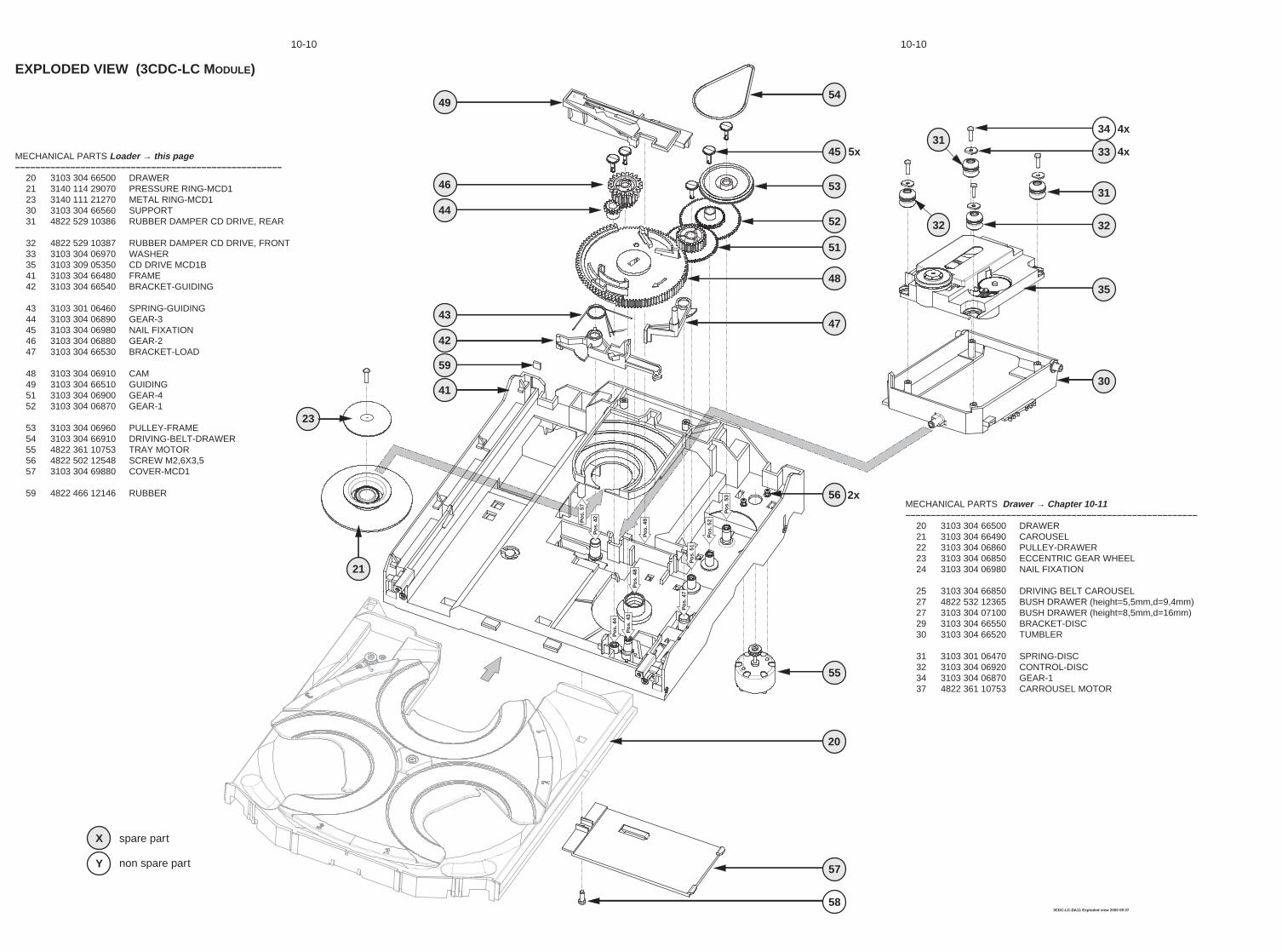
3CDC-LC-DA11 Exploded view 2000 09 07
Po
s. 5
1
Po
s. 5
3
Po
s. 5
2
Po
s. 4
7
Po
s. 4
8
Po
s. 4
9
Po
s. 4
3
Po
s. 4
4
Po
s. 4
2
Po
s. 5
7
54
53
47
55
56
31
30
35
32
31
32
33
34
X spare part
non spare partY 57
58
52
48
45 5x 4x
4x
46
49
44
43
42
59
41
21
20
51
23
2x
EXPLODED VIEW (3CDC-LC MODULE)
MECHANICAL PARTS Loader → this page–––––––––––––––––––––––––––––––––––––––––––––––––––––
20 3103 304 66500 DRAWER21 3140 114 29070 PRESSURE RING-MCD123 3140 111 21270 METAL RING-MCD130 3103 304 66560 SUPPORT31 4822 529 10386 RUBBER DAMPER CD DRIVE, REAR
32 4822 529 10387 RUBBER DAMPER CD DRIVE, FRONT33 3103 304 06970 WASHER35 3103 309 05350 CD DRIVE MCD1B41 3103 304 66480 FRAME42 3103 304 66540 BRACKET-GUIDING
43 3103 301 06460 SPRING-GUIDING44 3103 304 06890 GEAR-345 3103 304 06980 NAIL FIXATION46 3103 304 06880 GEAR-247 3103 304 66530 BRACKET-LOAD
48 3103 304 06910 CAM49 3103 304 66510 GUIDING51 3103 304 06900 GEAR-452 3103 304 06870 GEAR-1
53 3103 304 06960 PULLEY-FRAME54 3103 304 66910 DRIVING-BELT-DRAWER55 4822 361 10753 TRAY MOTOR56 4822 502 12548 SCREW M2,6X3,557 3103 304 69880 COVER-MCD1
59 4822 466 12146 RUBBERMECHANICAL PARTS Drawer → Chapter 10-11––––––––––––––––––––––––––––––––––––––––––––––––––––––––––
20 3103 304 66500 DRAWER21 3103 304 66490 CAROUSEL22 3103 304 06860 PULLEY-DRAWER23 3103 304 06850 ECCENTRIC GEAR WHEEL24 3103 304 06980 NAIL FIXATION
25 3103 304 66850 DRIVING BELT CAROUSEL27 4822 532 12365 BUSH DRAWER (height=5,5mm,d=9,4mm)27 3103 304 07100 BUSH DRAWER (height=8,5mm,d=16mm)29 3103 304 66550 BRACKET-DISC30 3103 304 66520 TUMBLER
31 3103 301 06470 SPRING-DISC32 3103 304 06920 CONTROL-DISC34 3103 304 06870 GEAR-137 4822 361 10753 CARROUSEL MOTOR
10-10 10-10
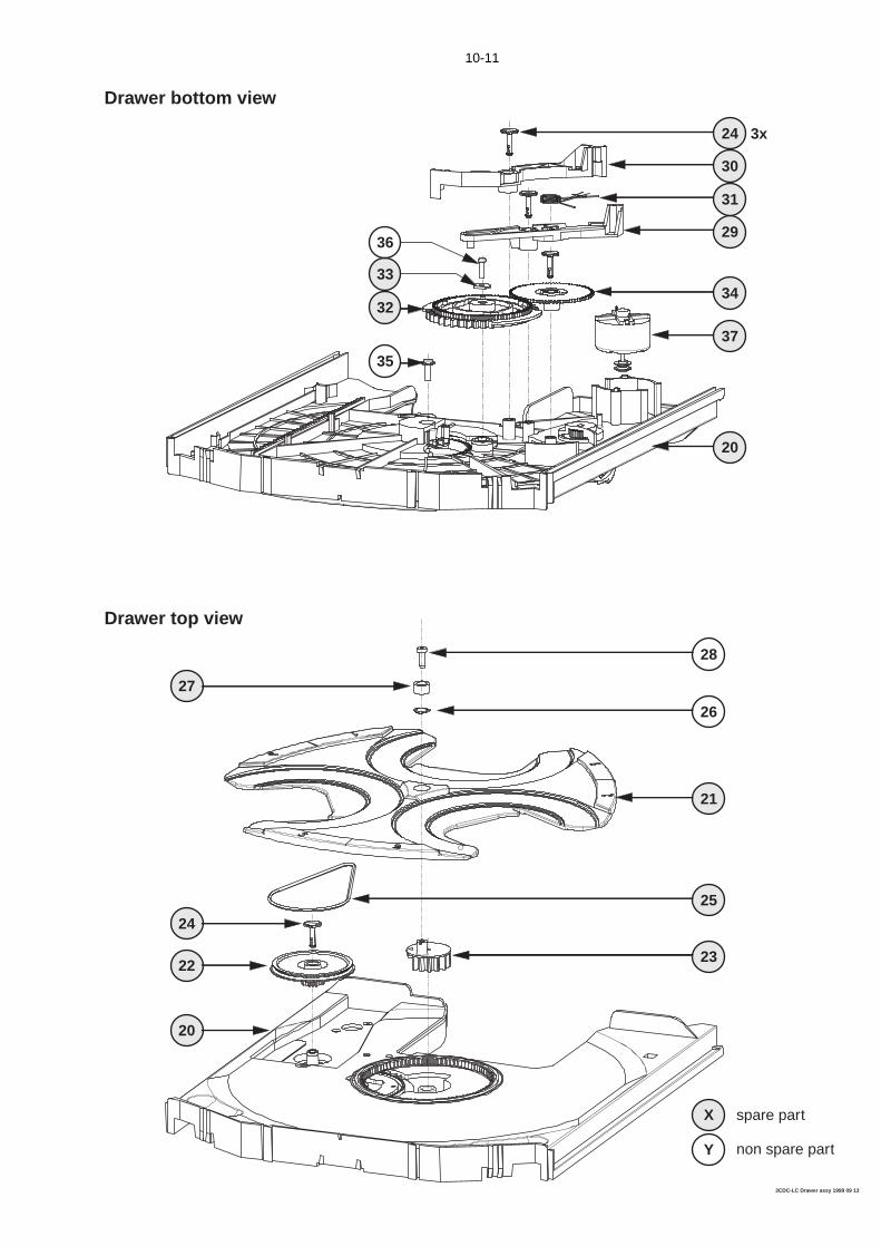
10-11
3CDC-LC Drawer assy 1999 09 13
37
20
32
35
33
3629
31
34
24
30
3x
27
24
22
20
23
25
21
26
28
Drawer top view
Drawer bottom view
X spare part
non spare partY
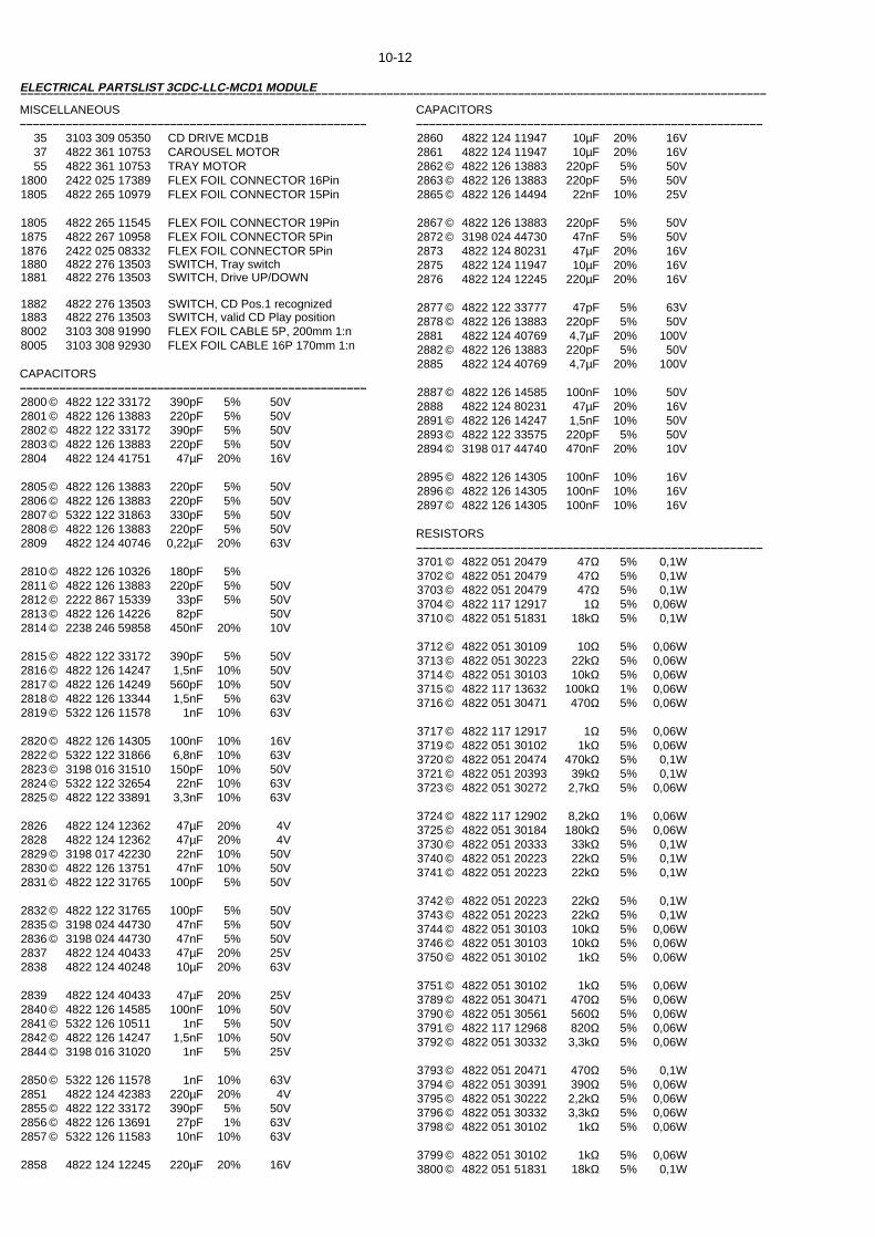
10-12
MISCELLANEOUS–––––––––––––––––––––––––––––––––––––––––––––––––––––
35 3103 309 05350 CD DRIVE MCD1B37 4822 361 10753 CAROUSEL MOTOR55 4822 361 10753 TRAY MOTOR
1800 2422 025 17389 FLEX FOIL CONNECTOR 16Pin1805 4822 265 10979 FLEX FOIL CONNECTOR 15Pin
1805 4822 265 11545 FLEX FOIL CONNECTOR 19Pin1875 4822 267 10958 FLEX FOIL CONNECTOR 5Pin1876 2422 025 08332 FLEX FOIL CONNECTOR 5Pin1880 4822 276 13503 SWITCH, Tray switch1881 4822 276 13503 SWITCH, Drive UP/DOWN
1882 4822 276 13503 SWITCH, CD Pos.1 recognized1883 4822 276 13503 SWITCH, valid CD Play position8002 3103 308 91990 FLEX FOIL CABLE 5P, 200mm 1:n8005 3103 308 92930 FLEX FOIL CABLE 16P 170mm 1:n
CAPACITORS–––––––––––––––––––––––––––––––––––––––––––––––––––––2800 © 4822 122 33172 390pF 5% 50V2801 © 4822 126 13883 220pF 5% 50V2802 © 4822 122 33172 390pF 5% 50V2803 © 4822 126 13883 220pF 5% 50V2804 4822 124 41751 47µF 20% 16V
2805 © 4822 126 13883 220pF 5% 50V2806 © 4822 126 13883 220pF 5% 50V2807 © 5322 122 31863 330pF 5% 50V2808 © 4822 126 13883 220pF 5% 50V2809 4822 124 40746 0,22µF 20% 63V
2810 © 4822 126 10326 180pF 5%2811 © 4822 126 13883 220pF 5% 50V2812 © 2222 867 15339 33pF 5% 50V2813 © 4822 126 14226 82pF 50V2814 © 2238 246 59858 450nF 20% 10V
2815 © 4822 122 33172 390pF 5% 50V2816 © 4822 126 14247 1,5nF 10% 50V2817 © 4822 126 14249 560pF 10% 50V2818 © 4822 126 13344 1,5nF 5% 63V2819 © 5322 126 11578 1nF 10% 63V
2820 © 4822 126 14305 100nF 10% 16V2822 © 5322 122 31866 6,8nF 10% 63V2823 © 3198 016 31510 150pF 10% 50V2824 © 5322 122 32654 22nF 10% 63V2825 © 4822 122 33891 3,3nF 10% 63V
2826 4822 124 12362 47µF 20% 4V2828 4822 124 12362 47µF 20% 4V2829 © 3198 017 42230 22nF 10% 50V2830 © 4822 126 13751 47nF 10% 50V2831 © 4822 122 31765 100pF 5% 50V
2832 © 4822 122 31765 100pF 5% 50V2835 © 3198 024 44730 47nF 5% 50V2836 © 3198 024 44730 47nF 5% 50V2837 4822 124 40433 47µF 20% 25V2838 4822 124 40248 10µF 20% 63V
2839 4822 124 40433 47µF 20% 25V2840 © 4822 126 14585 100nF 10% 50V2841 © 5322 126 10511 1nF 5% 50V2842 © 4822 126 14247 1,5nF 10% 50V2844 © 3198 016 31020 1nF 5% 25V
2850 © 5322 126 11578 1nF 10% 63V2851 4822 124 42383 220µF 20% 4V2855 © 4822 122 33172 390pF 5% 50V2856 © 4822 126 13691 27pF 1% 63V2857 © 5322 126 11583 10nF 10% 63V
2858 4822 124 12245 220µF 20% 16V
CAPACITORS–––––––––––––––––––––––––––––––––––––––––––––––––––––2860 4822 124 11947 10µF 20% 16V2861 4822 124 11947 10µF 20% 16V2862 © 4822 126 13883 220pF 5% 50V2863 © 4822 126 13883 220pF 5% 50V2865 © 4822 126 14494 22nF 10% 25V
2867 © 4822 126 13883 220pF 5% 50V2872 © 3198 024 44730 47nF 5% 50V2873 4822 124 80231 47µF 20% 16V2875 4822 124 11947 10µF 20% 16V2876 4822 124 12245 220µF 20% 16V
2877 © 4822 122 33777 47pF 5% 63V2878 © 4822 126 13883 220pF 5% 50V2881 4822 124 40769 4,7µF 20% 100V2882 © 4822 126 13883 220pF 5% 50V2885 4822 124 40769 4,7µF 20% 100V
2887 © 4822 126 14585 100nF 10% 50V2888 4822 124 80231 47µF 20% 16V2891 © 4822 126 14247 1,5nF 10% 50V2893 © 4822 122 33575 220pF 5% 50V2894 © 3198 017 44740 470nF 20% 10V
2895 © 4822 126 14305 100nF 10% 16V2896 © 4822 126 14305 100nF 10% 16V2897 © 4822 126 14305 100nF 10% 16V
RESISTORS–––––––––––––––––––––––––––––––––––––––––––––––––––––3701 © 4822 051 20479 47Ω 5% 0,1W3702 © 4822 051 20479 47Ω 5% 0,1W3703 © 4822 051 20479 47Ω 5% 0,1W3704 © 4822 117 12917 1Ω 5% 0,06W3710 © 4822 051 51831 18kΩ 5% 0,1W
3712 © 4822 051 30109 10Ω 5% 0,06W3713 © 4822 051 30223 22kΩ 5% 0,06W3714 © 4822 051 30103 10kΩ 5% 0,06W3715 © 4822 117 13632 100kΩ 1% 0,06W3716 © 4822 051 30471 470Ω 5% 0,06W
3717 © 4822 117 12917 1Ω 5% 0,06W3719 © 4822 051 30102 1kΩ 5% 0,06W3720 © 4822 051 20474 470kΩ 5% 0,1W3721 © 4822 051 20393 39kΩ 5% 0,1W3723 © 4822 051 30272 2,7kΩ 5% 0,06W
3724 © 4822 117 12902 8,2kΩ 1% 0,06W3725 © 4822 051 30184 180kΩ 5% 0,06W3730 © 4822 051 20333 33kΩ 5% 0,1W3740 © 4822 051 20223 22kΩ 5% 0,1W3741 © 4822 051 20223 22kΩ 5% 0,1W
3742 © 4822 051 20223 22kΩ 5% 0,1W3743 © 4822 051 20223 22kΩ 5% 0,1W3744 © 4822 051 30103 10kΩ 5% 0,06W3746 © 4822 051 30103 10kΩ 5% 0,06W3750 © 4822 051 30102 1kΩ 5% 0,06W
3751 © 4822 051 30102 1kΩ 5% 0,06W3789 © 4822 051 30471 470Ω 5% 0,06W3790 © 4822 051 30561 560Ω 5% 0,06W3791 © 4822 117 12968 820Ω 5% 0,06W3792 © 4822 051 30332 3,3kΩ 5% 0,06W
3793 © 4822 051 20471 470Ω 5% 0,1W3794 © 4822 051 30391 390Ω 5% 0,06W3795 © 4822 051 30222 2,2kΩ 5% 0,06W3796 © 4822 051 30332 3,3kΩ 5% 0,06W3798 © 4822 051 30102 1kΩ 5% 0,06W
3799 © 4822 051 30102 1kΩ 5% 0,06W3800 © 4822 051 51831 18kΩ 5% 0,1W
ELECTRICAL PARTSLIST 3CDC-LLC-MCD1 MODULE––––––––––––––––––––––––––––––––––––––––––––––––––––––––––––––––––––––––––––––––––––––––––––––––––––––––––––––––––
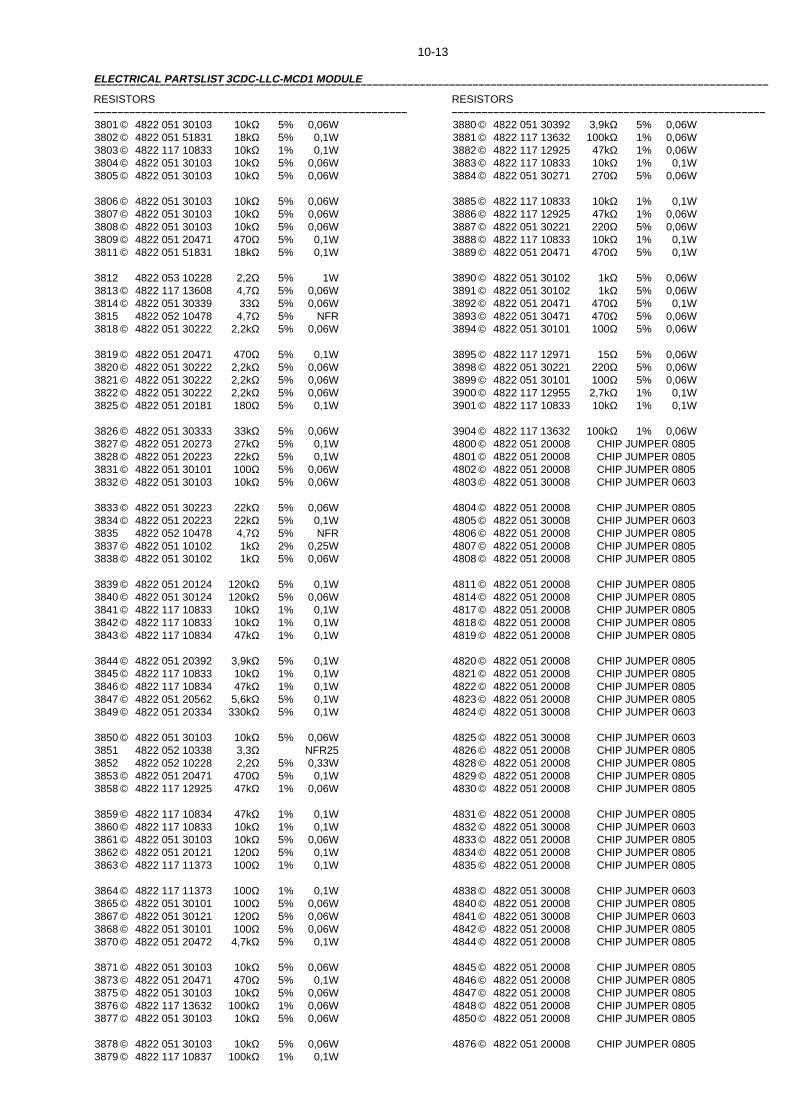
10-13
RESISTORS–––––––––––––––––––––––––––––––––––––––––––––––––––––3801 © 4822 051 30103 10kΩ 5% 0,06W3802 © 4822 051 51831 18kΩ 5% 0,1W3803 © 4822 117 10833 10kΩ 1% 0,1W3804 © 4822 051 30103 10kΩ 5% 0,06W3805 © 4822 051 30103 10kΩ 5% 0,06W
3806 © 4822 051 30103 10kΩ 5% 0,06W3807 © 4822 051 30103 10kΩ 5% 0,06W3808 © 4822 051 30103 10kΩ 5% 0,06W3809 © 4822 051 20471 470Ω 5% 0,1W3811 © 4822 051 51831 18kΩ 5% 0,1W
3812 4822 053 10228 2,2Ω 5% 1W3813 © 4822 117 13608 4,7Ω 5% 0,06W3814 © 4822 051 30339 33Ω 5% 0,06W3815 4822 052 10478 4,7Ω 5% NFR3818 © 4822 051 30222 2,2kΩ 5% 0,06W
3819 © 4822 051 20471 470Ω 5% 0,1W3820 © 4822 051 30222 2,2kΩ 5% 0,06W3821 © 4822 051 30222 2,2kΩ 5% 0,06W3822 © 4822 051 30222 2,2kΩ 5% 0,06W3825 © 4822 051 20181 180Ω 5% 0,1W
3826 © 4822 051 30333 33kΩ 5% 0,06W3827 © 4822 051 20273 27kΩ 5% 0,1W3828 © 4822 051 20223 22kΩ 5% 0,1W3831 © 4822 051 30101 100Ω 5% 0,06W3832 © 4822 051 30103 10kΩ 5% 0,06W
3833 © 4822 051 30223 22kΩ 5% 0,06W3834 © 4822 051 20223 22kΩ 5% 0,1W3835 4822 052 10478 4,7Ω 5% NFR3837 © 4822 051 10102 1kΩ 2% 0,25W3838 © 4822 051 30102 1kΩ 5% 0,06W
3839 © 4822 051 20124 120kΩ 5% 0,1W3840 © 4822 051 30124 120kΩ 5% 0,06W3841 © 4822 117 10833 10kΩ 1% 0,1W3842 © 4822 117 10833 10kΩ 1% 0,1W3843 © 4822 117 10834 47kΩ 1% 0,1W
3844 © 4822 051 20392 3,9kΩ 5% 0,1W3845 © 4822 117 10833 10kΩ 1% 0,1W3846 © 4822 117 10834 47kΩ 1% 0,1W3847 © 4822 051 20562 5,6kΩ 5% 0,1W3849 © 4822 051 20334 330kΩ 5% 0,1W
3850 © 4822 051 30103 10kΩ 5% 0,06W3851 4822 052 10338 3,3Ω NFR253852 4822 052 10228 2,2Ω 5% 0,33W3853 © 4822 051 20471 470Ω 5% 0,1W3858 © 4822 117 12925 47kΩ 1% 0,06W
3859 © 4822 117 10834 47kΩ 1% 0,1W3860 © 4822 117 10833 10kΩ 1% 0,1W3861 © 4822 051 30103 10kΩ 5% 0,06W3862 © 4822 051 20121 120Ω 5% 0,1W3863 © 4822 117 11373 100Ω 1% 0,1W
3864 © 4822 117 11373 100Ω 1% 0,1W3865 © 4822 051 30101 100Ω 5% 0,06W3867 © 4822 051 30121 120Ω 5% 0,06W3868 © 4822 051 30101 100Ω 5% 0,06W3870 © 4822 051 20472 4,7kΩ 5% 0,1W
3871 © 4822 051 30103 10kΩ 5% 0,06W3873 © 4822 051 20471 470Ω 5% 0,1W3875 © 4822 051 30103 10kΩ 5% 0,06W3876 © 4822 117 13632 100kΩ 1% 0,06W3877 © 4822 051 30103 10kΩ 5% 0,06W
3878 © 4822 051 30103 10kΩ 5% 0,06W3879 © 4822 117 10837 100kΩ 1% 0,1W
RESISTORS–––––––––––––––––––––––––––––––––––––––––––––––––––––3880 © 4822 051 30392 3,9kΩ 5% 0,06W3881 © 4822 117 13632 100kΩ 1% 0,06W3882 © 4822 117 12925 47kΩ 1% 0,06W3883 © 4822 117 10833 10kΩ 1% 0,1W3884 © 4822 051 30271 270Ω 5% 0,06W
3885 © 4822 117 10833 10kΩ 1% 0,1W3886 © 4822 117 12925 47kΩ 1% 0,06W3887 © 4822 051 30221 220Ω 5% 0,06W3888 © 4822 117 10833 10kΩ 1% 0,1W3889 © 4822 051 20471 470Ω 5% 0,1W
3890 © 4822 051 30102 1kΩ 5% 0,06W3891 © 4822 051 30102 1kΩ 5% 0,06W3892 © 4822 051 20471 470Ω 5% 0,1W3893 © 4822 051 30471 470Ω 5% 0,06W3894 © 4822 051 30101 100Ω 5% 0,06W
3895 © 4822 117 12971 15Ω 5% 0,06W3898 © 4822 051 30221 220Ω 5% 0,06W3899 © 4822 051 30101 100Ω 5% 0,06W3900 © 4822 117 12955 2,7kΩ 1% 0,1W3901 © 4822 117 10833 10kΩ 1% 0,1W
3904 © 4822 117 13632 100kΩ 1% 0,06W4800 © 4822 051 20008 CHIP JUMPER 08054801 © 4822 051 20008 CHIP JUMPER 08054802 © 4822 051 20008 CHIP JUMPER 08054803 © 4822 051 30008 CHIP JUMPER 0603
4804 © 4822 051 20008 CHIP JUMPER 08054805 © 4822 051 30008 CHIP JUMPER 06034806 © 4822 051 20008 CHIP JUMPER 08054807 © 4822 051 20008 CHIP JUMPER 08054808 © 4822 051 20008 CHIP JUMPER 0805
4811 © 4822 051 20008 CHIP JUMPER 08054814 © 4822 051 20008 CHIP JUMPER 08054817 © 4822 051 20008 CHIP JUMPER 08054818 © 4822 051 20008 CHIP JUMPER 08054819 © 4822 051 20008 CHIP JUMPER 0805
4820 © 4822 051 20008 CHIP JUMPER 08054821 © 4822 051 20008 CHIP JUMPER 08054822 © 4822 051 20008 CHIP JUMPER 08054823 © 4822 051 20008 CHIP JUMPER 08054824 © 4822 051 30008 CHIP JUMPER 0603
4825 © 4822 051 30008 CHIP JUMPER 06034826 © 4822 051 20008 CHIP JUMPER 08054828 © 4822 051 20008 CHIP JUMPER 08054829 © 4822 051 20008 CHIP JUMPER 08054830 © 4822 051 20008 CHIP JUMPER 0805
4831 © 4822 051 20008 CHIP JUMPER 08054832 © 4822 051 30008 CHIP JUMPER 06034833 © 4822 051 20008 CHIP JUMPER 08054834 © 4822 051 20008 CHIP JUMPER 08054835 © 4822 051 20008 CHIP JUMPER 0805
4838 © 4822 051 30008 CHIP JUMPER 06034840 © 4822 051 20008 CHIP JUMPER 08054841 © 4822 051 30008 CHIP JUMPER 06034842 © 4822 051 20008 CHIP JUMPER 08054844 © 4822 051 20008 CHIP JUMPER 0805
4845 © 4822 051 20008 CHIP JUMPER 08054846 © 4822 051 20008 CHIP JUMPER 08054847 © 4822 051 20008 CHIP JUMPER 08054848 © 4822 051 20008 CHIP JUMPER 08054850 © 4822 051 20008 CHIP JUMPER 0805
4876 © 4822 051 20008 CHIP JUMPER 0805
ELECTRICAL PARTSLIST 3CDC-LLC-MCD1 MODULE––––––––––––––––––––––––––––––––––––––––––––––––––––––––––––––––––––––––––––––––––––––––––––––––––––––––––––––––––
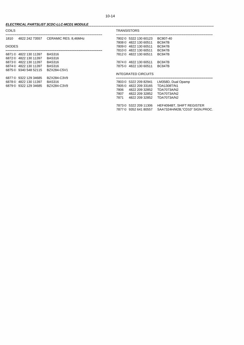
10-14
COILS–––––––––––––––––––––––––––––––––––––––––––––––––––––1810 4822 242 73557 CERAMIC RES. 8,46MHz
DIODES–––––––––––––––––––––––––––––––––––––––––––––––––––––6871 © 4822 130 11397 BAS3166872 © 4822 130 11397 BAS3166873 © 4822 130 11397 BAS3166874 © 4822 130 11397 BAS3166875 © 9340 548 52115 BZX284-C5V1
6877 © 9322 129 34685 BZX284-C3V96878 © 4822 130 11397 BAS3166879 © 9322 129 34685 BZX284-C3V9
TRANSISTORS–––––––––––––––––––––––––––––––––––––––––––––––––––––7802 © 5322 130 60123 BC807-407808 © 4822 130 60511 BC847B7809 © 4822 130 60511 BC847B7810 © 4822 130 60511 BC847B7812 © 4822 130 60511 BC847B
7874 © 4822 130 60511 BC847B7875 © 4822 130 60511 BC847B
INTEGRATED CIRCUITS–––––––––––––––––––––––––––––––––––––––––––––––––––––7803 © 5322 209 82941 LM358D, Dual Opamp7805 © 4822 209 33165 TDA1308T/N17806 4822 209 32852 TDA7073A/N27807 4822 209 32852 TDA7073A/N27871 4822 209 32852 TDA7073A/N2
7873 © 5322 209 11306 HEF4094BT, SHIFT REGISTER7877 © 9352 641 80557 SAA7324H/M2B,“CD10“ SIGN.PROC.
ELECTRICAL PARTSLIST 3CDC-LLC-MCD1 MODULE––––––––––––––––––––––––––––––––––––––––––––––––––––––––––––––––––––––––––––––––––––––––––––––––––––––––––––––––––
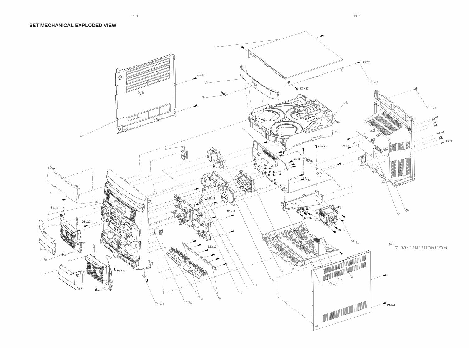
11-1 11-1
SET MECHANICAL EXPLODED VIEW
D3 x 10
D3 x 12
D3 x 10
D3 x 10
D3 x 12
D3 x 12
M2 x 3
D3 x 10
D3 x 10
D3 x 10
D3 x 10
D3 x 12
M3 x 6
M3 x 6
1401
D3 x 10
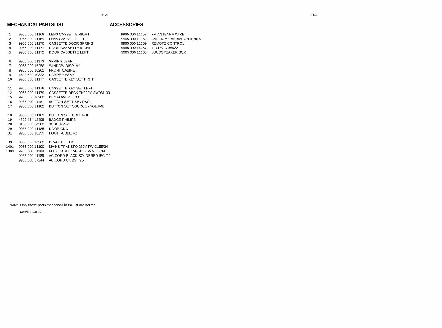
11-2 11-2
MECHANICAL PARTSLIST ACCESSORIES
1 9965 000 11168 LENS CASSETTE RIGHT 9965 000 11157 FM ANTENNA WIRE2 9965 000 11169 LENS CASSETTE LEFT 9965 000 11162 AM FRAME AERIAL ANTENNA3 9965 000 11170 CASSETTE DOOR SPRING 9965 000 11159 REMOTE CONTROL 4 9965 000 11171 DOOR CASSETTE RIGHT 9965 000 16257 IFU FW-C155/225 9965 000 11172 DOOR CASSETTE LEFT 9965 000 11163 LOUDSPEAKER BOX
6 9965 000 11173 SPRING LEAF7 9965 000 16258 WINDOW DISPLAY8 9965 000 16261 FRONT CABINET9 4822 529 10322 DAMPER ASSY
10 9965 000 11177 CASSETTE KEY SET RIGHT
11 9965 000 11178 CASSETTE KEY SET LEFT12 9965 000 11179 CASSETTE DECK TK20FX-SW981-00115 9965 000 16260 KEY POWER ECO16 9965 000 11181 BUTTON SET DBB / DSC17 9965 000 11182 BUTTON SET SOURCE / VOLUME
18 9965 000 11183 BUTTON SET CONTROL19 4822 454 13408 BADGE PHILIPS28 3103 308 54360 3CDC ASSY29 9965 000 11185 DOOR CDC31 9965 000 16259 FOOT RUBBER-2
33 9965 000 16262 BRACKET FTD1401 9965 000 11190 MAINS TRANSFO 230V FW-C155/341800 9965 000 11188 FLEX CABLE 15PIN 1,25MM 35CM
9965 000 11189 AC CORD BLACK SOLDERED IEC /22
Note: Only these parts mentioned in the list are normal
service parts.
9965 000 17244 AC CORD UK 2M /25


