Embed Size (px)
Citation preview
ARTICLE IN PRESS
Energy Policy 36 (2008) 4390–4396
Contents lists available at ScienceDirect
Energy Policy
0301-42
doi:10.1
$ Wh
are thos
Governm� Corr
E-m
journal homepage: www.elsevier.com/locate/enpol
Photovoltaic technologies$
Darren M. Bagnall a,�, Matt Boreland b
a Electronics and Computer Science, University of Southampton, Southampton SO17 1BJ, UKb School of Photovoltaic and Renewable Energy Engineering, University of New South Wales, Sydney NSW 2052, Australia
a r t i c l e i n f o
Keywords:
Silicon
Cadmium telluride
Thin-film semiconductor
15/$ - see front matter & 2008 Queen’s Print
016/j.enpol.2008.09.070
ile the Government Office for Science commis
e of the author(s), are independent of Govern
ent policy.
esponding author. Tel.: +44 0 23 8059 7609; f
ail address: [email protected] (D.M. Bagna
a b s t r a c t
Photovoltaics is already a billion dollar industry. It is experiencing rapid growth as concerns over fuel
supplies and carbon emissions mean that governments and individuals are increasingly prepared to
ignore its current high costs. It will become truly mainstream when its costs are comparable to other
energy sources. At the moment, it is around four times too expensive for competitive commercial
production. Three generations of photovoltaics have been envisaged that will take solar power into the
mainstream. Currently, photovoltaic production is 90% first-generation and is based on silicon wafers.
These devices are reliable and durable, but half of the cost is the silicon wafer and efficiencies are
limited to around 20%. A second generation of solar cells would use cheap semiconductor thin films
deposited on low-cost substrates to produce devices of slightly lower efficiency. A number of thin-film
device technologies account for around 5–6% of the current market. As second-generation technology
reduces the cost of active material, the substrate will eventually be the cost limit and higher efficiency
will be needed to maintain the cost-reduction trend. Third-generation devices will use new
technologies to produce high-efficiency devices. Advances in nanotechnology, photonics, optical
metamaterials, plasmonics and semiconducting polymer sciences offer the prospect of cost-competitive
photovoltaics. It is reasonable to expect that cost reductions, a move to second-generation technologies
and the implementation of new technologies and third-generation concepts can lead to fully cost-
competitive solar energy in 10–15 years.
& 2008 Queen’s Printer and Controller of HMSO. Published by Elsevier Ltd. All rights reserved.
1. Introduction
Why photovoltaics? There was a time when this was a difficultquestion to answer. Fossil fuel was plentiful and apparentlywithout end, and the Earth’s environment appeared resilient. Thephotovoltaic (PV) industry was based on the niche applications ofpowering satellites and remote locations. However, the tide haschanged dramatically, with growing recognition of the environ-mental impact of non-renewable energy sources and the econom-ic volatility that comes from reliance on oil and gas.
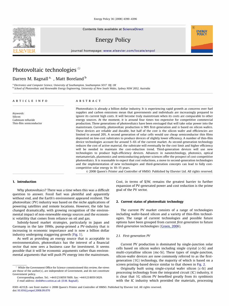
Subsidy-based market strategies, particularly in Japan andGermany in the late 1990s, pump-primed a PV-industry that isincreasing in economic importance and is now a billion dollarindustry undergoing staggering growth (Fig. 1).
As well as providing an energy source that is acceptable toenvironmentalists, photovoltaics has the interest of a financialsector that now sees a business case for investment. It seemspossible that it will be economic arguments rather than environ-mental arguments that will push PV energy into the mainstream.
er and Controller of HMSO. Publish
sioned this review, the views
ment, and do not constitute
ax: +44 0 23 8059 3029.
ll).
Cost, in terms of $/W, remains the greatest barrier to furtherexpansion of PV-generated power and cost reduction is the primegoal of the PV sector.
2. Current status of photovoltaic technology
The current PV market consists of a range of technologiesincluding wafer-based silicon and a variety of thin-film technol-ogies. The range of current technologies and possible futureoptions have been grouped from current first-generation to futurethird-generation technologies (Green, 2006).
2.1. First-generation PV
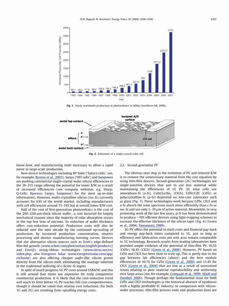
Current PV production is dominated by single-junction solarcells based on silicon wafers including single crystal (c-Si) andmulti-crystalline silicon (mc-Si). These types of single-junction,silicon-wafer devices are now commonly referred to as the first-generation (1G) technology, the majority of which is based on ascreen printing-based device similar to that shown in Fig. 2.
Originally built using single-crystal wafer silicon (c-Si) andprocessing technology from the integrated circuit (IC) industry, itis clear that 1G silicon PV benefited greatly from its symbiosiswith the IC industry which provided the materials, processing
ed by Elsevier Ltd. All rights reserved.
ARTICLE IN PRESS
4000
3500
3000
2500
2000
1500
1000
500
01993
69.1 69.4 77.6 88.6 125.8 154.9 199.9288.5 401.4
557.8759
1196
1771.2
2473.7
3733
1994 1995 1996 1997 1998 1999 2000
Year
Wor
ldw
ide
Pho
tovo
ltaic
Cel
l Pro
duct
ion
(MW
p)
2001 2002 2003 2004 2005 2006 2007
Fig. 1. Yearly worldwide production in photovoltaics in MWp (EurObserv’ER, 2008).
Fig. 2. Schematic of a single-crystal solar cell.
D.M. Bagnall, M. Boreland / Energy Policy 36 (2008) 4390–4396 4391
know-how, and manufacturing tools necessary to allow a rapidmove to large-scale production.
New device technologies including BP Solar (‘Saturn cells’; see,for example, Bruton et al., 2003), Sanyo (‘HIT cells’) and Sunpowerare pushing commercial single-crystal wafer silicon efficiencies tothe 18–21% range offering the potential for lower $/W as a resultof increased efficiencies (see company websites, e.g. Sharp;Q-Cells; Kyocera; Sanyo; Sunpower) for the most up-to-dateinformation). However, multi-crystalline silicon (mc-Si) currentlyaccounts for 63% of the world market, including manufacturerswith cell efficiencies around 13–14% but at overall lower $/W cost.
Half of the cost of first-generation photovoltaics is the cost ofthe 200–250-mm-thick silicon wafer—a cost incurred for largelymechanical reasons since the majority of solar absorption occursin the top few tens of microns. So reduction of wafer thicknessoffers cost-reduction potential. Production costs will also bereduced over the next decade by the continued up-scaling ofproduction, by increased production concentration, smarterprocessing and shorter manufacturing learning curves. Devicesthat use alternative silicon sources such as Scott’s edge-definedfilm-fed growth (www.schott.com/photovoltaic/english/products/)and EverQ’s string-ribbon technologies (www.sitrus.net/en/index.php; also Evergreen Solar: www.evergreensolar.com/app/en/home) are also offering cheaper wafer-like silicon growndirectly from the silicon-melt, eliminating the wastage inherentin the traditional wafering of c-Si/mc-Si ingots.
In spite of much progress, 1G PV costs around US$4/W, and thisis still around four times too expensive for truly competitivecommercial production. It is likely that the cost-reduction trendwill reach its limit before 1G PV reaches full cost-competitiveness,though it should be noted that relative cost reductions (for both1G and 2G) are resulting from spiralling energy costs.
2.2. Second-generation PV
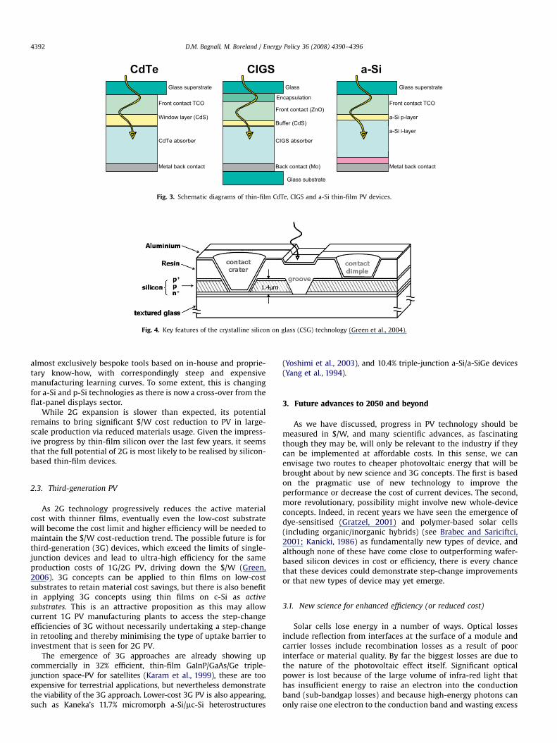
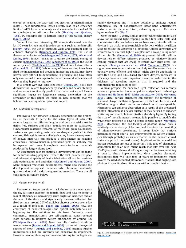
The obvious next step in the evolution of PV and reduced $/Wis to remove the unnecessary material from the cost equation byusing thin-film devices. Second-generation (2G) technologies aresingle-junction devices that aim to use less material whilemaintaining the efficiencies of 1G PV. 2G solar cells useamorphous-Si (a-Si), CuIn(Ga)Se2 (CIGS), CdTe/CdS (CdTe) orpolycrystalline-Si (p-Si) deposited on low-cost substrates suchas glass (Fig. 3). These technologies work because CdTe, CIGS anda-Si absorb the solar spectrum much more efficiently than c-Si ormc-Si and use only 1–10mm of active material. Meanwhile, in verypromising work of the last few years, p-Si has been demonstratedto produce �10% efficient devices using light-trapping schemes toincrease the effective thickness of the silicon layer (Fig. 4) (Greenet al., 2004; Yamamoto, 1999).
2G PV offers the potential to slash costs and financial pay-backand energy pay-back times compared to 1G, just as long asefficiency and fabrication costs per unit area remain comparableto 1G technology. Research results from leading laboratories haveprovided ample evidence of the potential of thin-film PV, 16.5%(CdTe), 18.4% (CIGS) (Green et al., 2006). However, PV based onCdTe and CIGS has been slow to scale up. This is partly due to thegap between lab efficiencies (above) and the best moduleefficiencies of 10.7% for CdTe (Green et al., 2006) and 13.4% forCIGS (Green et al., 2004) that are low as a result of unresolvedissues relating to poor material reproducibility and uniformityover large areas (see, for example, Compaan et al., 1999; Noufi andZweibel, 2006). Though perhaps the fundamental issue for bothCdTe and CIGS technologies is the historical absence of symbiosiswith a highly profitable IC industry. In comparison with silicon-wafer processes, thin-film process tools and production lines are
ARTICLE IN PRESS
Front contact TCO
Metal back contact
CdTe absorber
Window layer (CdS)
Glass superstrate
Front contact (ZnO)
Glass substrate
Back contact (Mo)
CIGS absorber
Buffer (CdS)
Glass
EncapsulationFront contact TCO
Metal back contact
a-Si i-layer
a-Si p-layer
Glass superstrate
Fig. 3. Schematic diagrams of thin-film CdTe, CIGS and a-Si thin-film PV devices.
Fig. 4. Key features of the crystalline silicon on glass (CSG) technology (Green et al., 2004).
D.M. Bagnall, M. Boreland / Energy Policy 36 (2008) 4390–43964392
almost exclusively bespoke tools based on in-house and proprie-tary know-how, with correspondingly steep and expensivemanufacturing learning curves. To some extent, this is changingfor a-Si and p-Si technologies as there is now a cross-over from theflat-panel displays sector.
While 2G expansion is slower than expected, its potentialremains to bring significant $/W cost reduction to PV in large-scale production via reduced materials usage. Given the impress-ive progress by thin-film silicon over the last few years, it seemsthat the full potential of 2G is most likely to be realised by silicon-based thin-film devices.
2.3. Third-generation PV
As 2G technology progressively reduces the active materialcost with thinner films, eventually even the low-cost substratewill become the cost limit and higher efficiency will be needed tomaintain the $/W cost-reduction trend. The possible future is forthird-generation (3G) devices, which exceed the limits of single-junction devices and lead to ultra-high efficiency for the sameproduction costs of 1G/2G PV, driving down the $/W (Green,2006). 3G concepts can be applied to thin films on low-costsubstrates to retain material cost savings, but there is also benefitin applying 3G concepts using thin films on c-Si as active
substrates. This is an attractive proposition as this may allowcurrent 1G PV manufacturing plants to access the step-changeefficiencies of 3G without necessarily undertaking a step-changein retooling and thereby minimising the type of uptake barrier toinvestment that is seen for 2G PV.
The emergence of 3G approaches are already showing upcommercially in 32% efficient, thin-film GaInP/GaAs/Ge triple-junction space-PV for satellites (Karam et al., 1999), these are tooexpensive for terrestrial applications, but nevertheless demonstratethe viability of the 3G approach. Lower-cost 3G PV is also appearing,such as Kaneka’s 11.7% micromorph a-Si/mc-Si heterostructures
(Yoshimi et al., 2003), and 10.4% triple-junction a-Si/a-SiGe devices(Yang et al., 1994).
3. Future advances to 2050 and beyond
As we have discussed, progress in PV technology should bemeasured in $/W, and many scientific advances, as fascinatingthough they may be, will only be relevant to the industry if theycan be implemented at affordable costs. In this sense, we canenvisage two routes to cheaper photovoltaic energy that will bebrought about by new science and 3G concepts. The first is basedon the pragmatic use of new technology to improve theperformance or decrease the cost of current devices. The second,more revolutionary, possibility might involve new whole-deviceconcepts. Indeed, in recent years we have seen the emergence ofdye-sensitised (Gratzel, 2001) and polymer-based solar cells(including organic/inorganic hybrids) (see Brabec and Sariciftci,2001; Kanicki, 1986) as fundamentally new types of device, andalthough none of these have come close to outperforming wafer-based silicon devices in cost or efficiency, there is every chancethat these devices could demonstrate step-change improvementsor that new types of device may yet emerge.
3.1. New science for enhanced efficiency (or reduced cost)
Solar cells lose energy in a number of ways. Optical lossesinclude reflection from interfaces at the surface of a module andcarrier losses include recombination losses as a result of poorinterface or material quality. By far the biggest losses are due tothe nature of the photovoltaic effect itself. Significant opticalpower is lost because of the large volume of infra-red light thathas insufficient energy to raise an electron into the conductionband (sub-bandgap losses) and because high-energy photons canonly raise one electron to the conduction band and wasting excess
ARTICLE IN PRESS
Fig. 5. SEM micrograph of a silicon ‘moth-eye’ antireflective surface (Boden and
Bagnall, 2006).
D.M. Bagnall, M. Boreland / Energy Policy 36 (2008) 4390–4396 4393
energy by heating the solar cell (hot-electron or thermalisationlosses). These fundamental losses directly lead to an efficiencylimit of �40% for all commonly used semiconductors and 43.9%for single-junction silicon solar cells (Shockley and Queisser,1961). 3G concepts aim to harness some of this wasted energy(Green, 2006).
Some of the most interesting 3G concepts discussed over thelast 30 years include multi-junction systems such as tandem cells(Henry, 1980), the use of quantum wells and quantum dots toenhance absorption (Barnham and Duggan, 1990), the use offluorescent collectors (Goetzberger and Greubel, 1977; Weber andLambe, 1976), impact ionisation to utilise the kinetic energy ofcarriers (Kolodinski et al., 1993; Landsberg et al., 1993), the use ofimpurity levels (Corkish and Green, 1993) and hot-electron effects(Ross and Nozik, 1982). While many of these exciting ideas havefired the imagination and provided interesting debate, most haveproven very difficult to demonstrate in principle and have oftenonly ever served to manage to decrease the overall efficiencies ofdevices they hoped to improve.
In a similar way, dye-sensitised cells (Gratzel, 2001) still facedifficult issues related to poor charge mobility and device stabilityand we cannot confidently predict that these devices will have asignificant impact on large-scale energy generation. In theremainder of this paper we focus on new concepts that webelieve can have significant practical impact.
3.2. Materials developments
Photovoltaic performance is heavily dependent on the proper-ties of materials. In particular, the active layers of solar cellsrequire long carrier diffusion lengths and bulk material must bedefect-free, surfaces and grain boundaries must be passivated.Fundamental materials research, of materials, grain boundaries,surfaces and passivating materials can always be justified in thiscontext. Although it seems unlikely that any future developmentsof known materials can produce a step-change in headlineefficiencies, improvements in production yield or stability canbe expected and research emphasis needs to be on materialsproduced by large-volume tools.
An exceptional case for materials developments can be madefor semiconducting polymers, where the vast parameter spaceand inherent simplicity of device fabrication allows for consider-able optimisation and optimism (McConnell and Matson, 2004).More complex ‘materials’ developments might also include thedevelopment of optical metamaterials, plasmonic materials,quantum dots and bandgap-engineering materials. These are allconsidered in context below.
3.3. Optical metamaterials
Photovoltaic arrays can either track the sun as it moves acrossthe sky (at some expense) or remain fixed and have to accept aloss of efficiency as increasingly acute angles of incidence reducethe area of the device and significantly increase reflection. Forfixed systems, around 20% of available photons are lost over a dayas a result of reflection (Boden and Bagnall, 2006), now, theemergence of nanotechnologies and optical metamaterials arebeginning to offer solutions to this issue. Currently, somecommercial manufacturers use self-organised nanostructuredglass surfaces to improve system efficiencies by around 10%(Wohlgemuth et al., 2005). More carefully constructed siliconnanostructures (Boden and Bagnall, 2006) that mimic the eyes ofspecies of moth (Vukusic and Sambles, 2003) promise furtherimprovements but are currently too expensive to implement.However, nano-embossing and nano-imprinting technologies are
rapidly developing and it is now possible to envisage regularcommercial use of nanostructured broad-band antireflectivesurfaces within the near future, enhancing system efficienciesby more than 10% (Fig. 5).
Over the next 10 years, similar optical technologies might alsoallow for improved light-trapping in thin-film solar cells andconcentrator cells (see below). As we have seen, thin-film silicondevices in particular require multiple reflections within the siliconlayer to ensure the absorption of photons. Optical constructs arerequired to ensure that light is coupled into a waveguiding modeof the thin film (Heine et al., 1996). At present, thin-film silicondevices rely on diffuse reflectors produced by relatively simpleetching regimes that are cheap to realise over large areas (forexample, Chuangsuwanich et al., 2004; Yamamoto, 1999). De-signed nanostructured surfaces are likely to offer routes that areoptically more efficient and which might also be applicable toultra-thin CdTe and CIGS-based thin-film devices. Increases inefficiency here are less important than the reduction in thethickness of absorbing material that is required and thecommensurate reduction in cost.
A final prospect for enhanced light collection has recentlyarisen as plasmonics has emerged as a significant technology(Bohren and Huffman, 1983; Maier and Atwater, 2005; Mulvaney,2001). Metal surface structures can support the formation ofresonant charge oscillations (plasmons) with finite lifetimes anddiffusion lengths that can be considered as a quasi-particle.Plasmonics can enhance absorption as a result of the prolongedphoton interaction at a device surface or may be used to enhancescattering and direct photons into thin absorbing layers. By tuningthe size of metallic nanostructures, it is possible to modify thewavelength response to cover a broad spectral range (Mulvaney,2001). Meanwhile, the non-locality of photons allows only arelatively sparse density of features and therefore the possibilityof inhomogeneous broadening. It seems likely that surfaceplasmonics might offer 5–10% improvements in system efficien-cies (though probably as an alternative to the nanostructuredsurface approach outlined above). Implications for material orprocess reduction are just as important. This type of plasmonicsapplication for solar cells might reach maturity over the next10–15 years, with chemical self-organising mechanisms providinga route to cheap implementation. More complex plasmonicpossibilities that will take tens of years to implement mightinvolve the used of coupled plasmonic structures that might guidephotons to specific absorption sites within complex devices.
ARTICLE IN PRESS
D.M. Bagnall, M. Boreland / Energy Policy 36 (2008) 4390–43964394
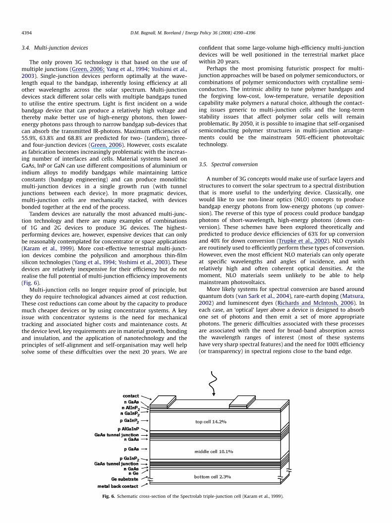
3.4. Multi-junction devices
The only proven 3G technology is that based on the use ofmultiple junctions (Green, 2006; Yang et al., 1994; Yoshimi et al.,2003). Single-junction devices perform optimally at the wave-length equal to the bandgap, inherently losing efficiency at allother wavelengths across the solar spectrum. Multi-junctiondevices stack different solar cells with multiple bandgaps tunedto utilise the entire spectrum. Light is first incident on a widebandgap device that can produce a relatively high voltage andthereby make better use of high-energy photons, then lower-energy photons pass through to narrow bandgap sub-devices thatcan absorb the transmitted IR-photons. Maximum efficiencies of55.9%, 63.8% and 68.8% are predicted for two- (tandem), three-and four-junction devices (Green, 2006). However, costs escalateas fabrication becomes increasingly problematic with the increas-ing number of interfaces and cells. Material systems based onGaAs, InP or GaN can use different compositions of aluminium orindium alloys to modify bandgaps while maintaining latticeconstants (bandgap engineering) and can produce monolithicmulti-junction devices in a single growth run (with tunneljunctions between each device). In more pragmatic devices,multi-junction cells are mechanically stacked, with devicesbonded together at the end of the process.
Tandem devices are naturally the most advanced multi-junc-tion technology and there are many examples of combinationsof 1G and 2G devices to produce 3G devices. The highest-performing devices are, however, expensive devices that can onlybe reasonably contemplated for concentrator or space applications(Karam et al., 1999). More cost-effective terrestrial multi-junct-ion devices combine the polysilicon and amorphous thin-filmsilicon technologies (Yang et al., 1994; Yoshimi et al., 2003). Thesedevices are relatively inexpensive for their efficiency but do notrealise the full potential of multi-junction efficiency improvements(Fig. 6).
Multi-junction cells no longer require proof of principle, butthey do require technological advances aimed at cost reduction.These cost reductions can come about by the capacity to producemuch cheaper devices or by using concentrator systems. A keyissue with concentrator systems is the need for mechanicaltracking and associated higher costs and maintenance costs. Atthe device level, key requirements are in material growth, bondingand insulation, and the application of nanotechnology and theprinciples of self-alignment and self-organisation may well helpsolve some of these difficulties over the next 20 years. We are
Fig. 6. Schematic cross-section of the Spectrola
confident that some large-volume high-efficiency multi-junctiondevices will be well positioned in the terrestrial market placewithin 20 years.
Perhaps the most promising futuristic prospect for multi-junction approaches will be based on polymer semiconductors, orcombinations of polymer semiconductors with crystalline semi-conductors. The intrinsic ability to tune polymer bandgaps andthe forgiving low-cost, low-temperature, versatile depositioncapability make polymers a natural choice, although the contact-ing issues generic to multi-junction cells and the long-termstability issues that affect polymer solar cells will remainproblematic. By 2050, it is possible to imagine that self-organisedsemiconducting polymer structures in multi-junction arrange-ments could be the mainstream 50%-efficient photovoltaictechnology.
3.5. Spectral conversion
A number of 3G concepts would make use of surface layers andstructures to convert the solar spectrum to a spectral distributionthat is more useful to the underlying device. Classically, onewould like to use non-linear optics (NLO) concepts to producebandgap energy photons from low-energy photons (up conver-sion). The reverse of this type of process could produce bandgapphotons of short-wavelength, high-energy photons (down con-version). These schemes have been explored theoretically andpredicted to produce device efficiencies of 63% for up conversionand 40% for down conversion (Trupke et al., 2002). NLO crystalsare routinely used to efficiently perform these types of conversion.However, even the most efficient NLO materials can only operateat specific wavelengths and angles of incidence, and withrelatively high and often coherent optical densities. At themoment, NLO materials seem unlikely to be able to helpmainstream photovoltaics.
More likely systems for spectral conversion are based aroundquantum dots (van Sark et al., 2004), rare-earth doping (Matsura,2002) and luminescent dyes (Richards and McIntosh, 2006). Ineach case, an ‘optical’ layer above a device is designed to absorbone set of photons and then emit a set of more appropriatephotons. The generic difficulties associated with these processesare associated with the need for broad-band absorption acrossthe wavelength ranges of interest (most of these systemshave very sharp spectral features) and the need for 100% efficiency(or transparency) in spectral regions close to the band edge.
b triple-junction cell (Karam et al., 1999).
ARTICLE IN PRESS
D.M. Bagnall, M. Boreland / Energy Policy 36 (2008) 4390–4396 4395
Broad-band absorption can be achieved by the use ofinhomogeneous broadening mechanisms. In the case of quantumdots, this would be readily achieved by changing the sizedistribution of the dots. For rare-earth doping systems, broad-ening requires variation in the material supporting the atoms andthis is more problematic. Meanwhile, mixtures of dyes are neededto broaden absorption. In each case, broadening the absorptionleads to broadening of the emission and this will normallydecrease the optical conversion efficiency.
It is therefore likely that spectral conversion will always be adifficult issue, and it seems unlikely that very-high-efficiencydevices could be created. We can, however, anticipate twopromising avenues for exploitation that might have an impacton commercial production. First, it seems highly probable thatquantum dots embedded in dielectric layers directly abovetraditional devices might readily add 3–5% to device efficiencywith little extra cost (van Sark et al., 2004). Second, spectralconversion could be applied within fluorescent collectors(Goetzberger and Greubel, 1977; Weber and Lambe, 1976), wherelarge-area waveguiding layers containing dye molecules, quantumdots or nanocrystals could be used to concentrate light into thesides of small-area pn junctions. Here the benefit is not high-efficiency devices, instead it is in semiconductor volume reduc-tion; two orders of magnitude less silicon might be needed toproduce 20% devices (Markvart, 2006).
3.6. Self-organised quantum devices and nanostructures
In addition to the possible use of quantum dots as spectralconverters, the use of quantum wells and quantum dots has alsobeen proposed to extend the bandgap (Barnham and Duggan,1990) and as a means to provide multiple electrons from a singlephoton through impact ionisation (Kolodinski et al., 1993; Rossand Nozik, 1982).
Quantum wells, wires or dots can be used to engineer thebandgap of materials. An example would be the growth of SiGequantum wells or Ge quantum dots by chemical vapour deposi-tion on a silicon wafer. The SiGe would provide regions ofnarrowed bandgap, allowing increased absorption in the infra-red.Invariably, such enhancements might result in increased absorp-tion, but the quantum features also introduce carrier traps andmore defective crystal growth, and this in turn leads to increasedcarrier recombination. To overcome this, quantum dots could existin a layer separated by a thin insulator, which should in principlereduce the loss mechanisms, but will also reduce carrier transferfrom dot to bulk semiconductor.
Impact ionisation is a process in which absorbed photons insemiconductors of at least twice the bandgap can producemultiple electron–hole pairs. Kolodinski et al. (1995) proposedthe use of Ge superlattices for this purpose. Alternatively, Si/Ge orSi/SiO2 superlattices could be used (Green, 2006), or certainquantum dots (Ellinson et al., 2005) that can generate two or threeexcitons (electron–hole pairs) per photon, which could tunnel ortransfer (via polariton modes) from surface layers into theconduction band of 1G or 2G devices and thereby increase theefficiency. The prospects for impact ionisation will be limited bythe finite flux of high-energy photons and the need for effects overa broad spectral range. As with some of the other concepts alreadydiscussed, the most likely practical implementation would be inthe simple addition of a cheap layer of self-organised structuresthat might add 2% or 3% to device efficiency.
A truly futuristic and nanotechnological approach to photo-voltaics might involve the use of self-organised structures. Most ofmainstream PV to date has been based on layered, large-areadevices. An alternative would be the use of arrays of high densities
of self-forming nanodevices. Many semiconductors have beengrown in nanowire or nanorod form (Kayes et al., 2005) viavapour–liquid–solid (VLS) techniques. It is also possible toimagine other seeded or selective growth techniques to providesmall high-quality crystallites that could also form the basis ofnanodevices. Advantages of such approaches would include thereduction of material volume, uniformity of device behaviour,good crystalline growth on amorphous substrates and prospectsfor multi-junctions.
4. Conclusions
Over the next 20 years, we can foresee only small improve-ments in the production efficiencies of 1G silicon technologies.However, we can expect fabrication, installation and operationalcost reductions (up to 30%) that will continue to provide reduced$/W and increasing completion. In the same period, we willwitness a change from predominantly 1G production to an era of2G devices probably based on thin-film silicon (up to 30% costreduction). While these two mainstreams will dominate thecommercial PV sector, we expect that we will see increasing use ofnew and 3G technologies that will enhance the performance(or reduce the cost) of 1G and 2G solar cells. These technologiesare very likely to include some multi-junction concepts andconstructs based on the emerging fields of optical metamaterials,plasmonics, quantum technology, nanotechnology and polymersemiconductor science.
By 2020 and possibly much sooner, we fully expect photo-voltaics to have become a truly cost-competitive energy supply,though the timing of this will depend on levels of researchinvestment, the levels of national, international and multinationalco-operation and the rate of increase in the cost of non-renewableenergy supplies.
References
Barnham, K.W.J., Duggan, G., 1990. A new approach to high-efficiency multi-band-gap solar cells. Journal of Applied Physics 67, 3490–3493.
Boden, S.A., Bagnall, D.M., 2006. Bio-mimetic subwavelength surface for near-zeroreflection sunrise to sunset. In: Proceedings of the Fourth World Conference onPhotovoltaic Energy Conversion, Hawaii.
Bohren, C.F., Huffman, D.R., 1983. Absorption and Scattering of Light by SmallParticles. Wiley, New York.
Brabec, C.J., Sariciftci, S.N., 2001. Recent developments in conjugated polymer-based plastic solar cells. Chemical Monthly 132, 421.
Bruton, T., Mason, N., Roberts, S., Hartley, O.N., Gledhill, S., Fernandez, J., Russell, R.,Warta, W., Glunz, S., Schultz, O., Hermle, M., Willeke, G., 2003. Towards 20%efficient silicon solar cells manufactured at 60 MWp per annum. In:Proceedings of the Third World Conference on Photovoltaic Energy Conversion,Osaka.
Chuangsuwanich, N., Widenborg, P.I., Campbell, P., Aberle, A.G., 2004. Technicaldigest. In: 14th International Photovoltaic Solar Energy Conference, Bangkok,325pp.
Compaan, A.D., Sites, J.R., Birkmire, R.W., Ferekides, C.S., Fahrenbruch, A.L., 1999.Critical issues and research needs for CdTe-based solar cells. In: Photovoltaicsfor the 21st Century, Electrochemical Society Symposium Proceedings, ECS99-11.
Corkish, R., Green, M.A., 1993. Recombination of carriers in quantum well solarcells. In: Conference Record, 23rd IEEE Photovoltaic Specialists’ Conference,Louisville, pp. 675–680.
Ellinson, R., Beard, M., Johnson, J., Yu, O.I., Micic, A., Shabaev, A., Efros, L., Nozik, A.J.,2005. Highly efficient multiple exciton generation in colloidal PbSe and PbSquantum dots. Nano Letters (American Chemical Society) 5 (5), 865–871.
EurObserv’ER, 2008. Photovoltaic Energy Barometer: /http://ec.europa.eu/energy/res/publications/barometers_en.htmS (accessed 25 May 2008).
Evergreensolar: /http://www.evergreensolar.com/app/en/home/S (accessed 25May 2008).
EverQ: /http://www.sitrus.net/en/index.phpS (accessed 25 May 2008).Goetzberger, A., Greubel, W., 1977. Solar-energy conversion with fluorescent
collectors. Applied Physics 14, 123–139.Gratzel, M., 2001. Photoelectrochemical cells. Nature 414, 338.Green, M., 2006. Third-Generation Photovoltaics: Advanced Solar Energy Conver-
sion. Springer, Berlin.
ARTICLE IN PRESS
D.M. Bagnall, M. Boreland / Energy Policy 36 (2008) 4390–43964396
Green, M., Basore, P.A., Chang, N., Clugston, D., Egan, R., Evans, R., Hogg, D.,Jarnason, S., Keevers, M., Lasswell, P., O’Sullivan, J., Schubert, U., Turner, A.,Wenham, S.R., Young, T., 2004. Crystalline silicon on glass (CSG) thin-film solarcell modules. Solar Energy Materials and Solar Cells 77, 857–863.
Green, M., Emery, K., King, D., Igari, S., Warta, W., 2006. Solar cell efficiency tables(Version 27). Progress in Photovoltaics: Research and Applications 14, 45–51.
Heine, C., Morf, R.H., Gale, M.T., 1996. Coated submicron gratings for broadbandantireflection in solar energy applications. Journal of Modern Optics 43,1371–1377.
Henry, C.H., 1980. Limiting efficiencies of ideal single- and multiple-energy-gapterrestrial solar cells. Journal of Applied Physics 51, 4494–4500.
Kanicki, J., 1986. Polymeric semiconductor contacts and photovoltaic applications.In: Skotheim, T.A. (Ed.), Handbook of Conducting Polymers. Dekker, New York.
Karam, N.H., King, R.R., Cavicchi, B.T., Krut, D.D., Ermer, J.H., Haddad, M., Cai Li,Joslin, D.E., Takahashi, M., Eldredge, J.W., Nishikawa, W.T., Lillington, D.R.,Keyes, B.M., Ahrenkiel, R.K., 1999. Development and characterization of high-efficiency Ga0.5In0.5P/GaAs/Ge dual- and triple-junction solar cells. IEEETransactions on Electron Devices 46 (10), 2116–2125.
Kayes, B.M., Richardson, C.E., Lewis, N.S., Atwater, H.A., 2005. Radial pn junctionnanorod solar cells: device physics principles and routes to fabrication insilicon. In: Conference Record, 31st IEEE Photovoltaic Specialists’ Conference,Orlando, vol. 1, 55p.
Kolodinski, S., Werner, J.H., Wittchen, T., Queisser, H.J., 1993. Quantum efficienciesexceeding unity due to impact ionization in silicon solar cells. Applied PhysicsLetters 63 (17), 2405–2407.
Kolodinski, S., Werner, J.H., Queisser, H.J., 1995. Applied Physics A 61, 535.Kyocera: /http://www.kyocerasolar.comS (accessed 25 May 2008).Landsberg, P.T., Nussbaumer, H., Willeke, G., 1993. Band–band impact ionization
and solar cell efficiency. Journal of Applied Physics 74, 1451.Maier, S.A., Atwater, H.A., 2005. Plasmonic: localization and guiding of electromagnetic
energy in metal/dielectric structures. Journal of Applied Physics 98, 01101.Markvart, T., 2006. Detailed balance method for ideal single-stage fluorescent
collectors. Journal of Applied Physics 99, 26101.Matsura, D., 2002. Structure property and visible upconversion of Er3+ doped
Gd2O3 nanocrystals. Applied Physics Letters 81, 4526.McConnell, R., Matson, R., 2004. Next-generation photovoltaic technologies in the
United States. In: Proceedings of the 19th European Photovoltaic Solar EnergyConference and Exhibition, Paris.
Mulvaney, P., 2001. Not all that is gold does glitter. MRS Bulletin 26, 1009–1014.
Noufi, R., Zweibel, K., 2006. High-efficiency CdTe and CIGS thin-film solar cells:highlights and challenges. In: Fourth World Conference on Photovoltaic EnergyConversion, Hawaii.
Q-Cells: /http://www.q-cells.comS (accessed 25 May 2008).Richards, B.S., McIntosh, K.R., 2006. Increased mc-Si module efficiency using
fluorescent organic dyes: a ray-tracing study. In: Proceedings of the FourthWorld Conference on Photovoltaic Energy Conversion, Hawaii.
Ross, R.T., Nozik, A.J., 1982. Efficiency of hot-carrier solar energy converters. Journalof Applied Physics 5, 3813–3818.
Sanyo: /http://www.sanyo.co.jp/clean/solar/hit_e/module.htmlS (accessed 25May 2008).
Scott: /http://www.schott.com/photovoltaic/english/products/S (accessed 25May 2008).
Sharp: /http://www.unlimited-power.co.uk/S (accessed 25 May 2008).Shockley, W., Queisser, H.J., 1961. Detailed balance limit of efficiency of p–n
junction solar cells. Journal of Applied Physics 32, 510.Sunpower: /http://www.sunpowercorp.comS (accessed 25 May 2008).Trupke, T., Green, M.A., Wurfel, P., 2002. Improving solar cell efficiencies by up-
conversion of sub-band-gap light. Journal of Applied Physics 92, 4117.Weber, W.H., Lambe, J., 1976. Limiting efficiencies of ideal single and multiple
energy gap terrestrial solar cells. Applied Optics 15, 2299.Wohlgemuth, J.H., Cunningham, D.W., Nguyen, A.M., Shaner, J., Ransome, S.J.,
Artigao, A., Fernandez, J.M., 2005. Increased energy collection using anti-reflective coated glass. In: 20th European Photovoltaic Solar Energy Con-ference, Barcelona.
van Sark, W.G.J.H.M., De Mello Donega, C., Harkisoen, C., Kinderman, R., vanRoosmalen, J.A.M., Schropp, R.E.I., Lysen, E.H., 2004. Improvement of spectralresponse of solar cells by deployment of spectral converters containingsemiconductor nanocrystals. In: Proceedings of the 19th European Photo-voltaic Solar Energy Conference, Paris.
Vukusic, P., Sambles, J.R., 2003. Photonic structures in biology. Nature 424,852–855.
Yamamoto, K., 1999. Very thin film crystalline silicon solar cells on glass substratefabricated at low temperature. Transactions on Electron Devices 46, 2041–2047.
Yang, J., Banerjee, A., Glatfelter, T., Hoffman, K., Xu, X., Guha, S., 1994. In: ConferenceRecord, First World Conference on Photovoltaic Energy Conversion, Hawaii, 380pp.
Yoshimi, M., Sasaki, T., Sawada, T., Suezaki, T., Meguro, T., Matsuda, T., Santo, K., Wadano,K., Ichikawa, M., Nakajima, A., Yamamoto, K., 2003. In: Conference Record, ThirdWorld Conference on Photovoltaic Energy Conversion, Osaka, 1566pp.


