Embed Size (px)
Citation preview

Optical Materials 33 (2011) 958–967
Contents lists available at ScienceDirect
Optical Materials
journal homepage: www.elsevier .com/locate /optmat
New aliphatic–aromatic tetraphenylphthalic-based diimides: Thermal, opticaland electrical study
Agnieszka Iwan a,⇑, Ewa Schab-Balcerzak b,c,⇑, Mariola Siwy b, Andrzej Sikora a, Marcin Palewicz a,Henryk Janeczek b, Maciej Sibinski d
a Electrotechnical Institute, Division of Electrotechnology and Materials Science, M. Sklodowskiej-Curie 55/61 Street, 50-369 Wroclaw, Polandb Centre of Polymer and Carbon Materials, Polish Academy of Sciences, 34 M. Curie-Sklodowska Street, 41-819 Zabrze, Polandc Institute of Chemistry, University of Silesia, Szkolna 9, 40-006 Katowice, Polandd Department of Semiconductor and Optoelectronic Devices, Technical University of Łódz, Poland
a r t i c l e i n f o a b s t r a c t
Article history:Received 2 July 2010Received in revised form 3 December 2010Accepted 27 December 2010Available online 18 February 2011
Keywords:ImidesAzomethinesLiquid crystalsThermotropic compoundsPhotovoltaic measurements
0925-3467/$ - see front matter � 2011 Elsevier B.V. Adoi:10.1016/j.optmat.2010.12.017
⇑ Corresponding authors. Address: Centre of PolyPolish Academy of Sciences, 34 M. Curie-Sklodowska(E. Schab-Balcerzak).
E-mail addresses: [email protected] (A. Iwan), eedu.pl, [email protected] (E. Schab-Balc
The thermal and opto-electrical properties of new thermotropic compounds based on tetraphenylphtha-lic-based imides have been explored. Energy band gap (Eopt:
g ) was calculated from absorption spectrumand absorption coefficient a. Current–voltage (I–V) measurements were performed on ITO/compound/Al, ITO/compound:PCBM/Al and ITO/PEDOT:PSS/compound:PCBM/Al devices before and after irradiationwith light (under illumination 1000 W/m2). Compounds were blended with [6,6]-phenyl C61 butyric acidmethyl ester (PCBM) in the weight ratio 1:1 and additionally tested using various AFM techniques. Themesogenic properties were characterized by POM and DSC. Both compounds exhibited liquid crystallineproperties. Preliminary photovoltaic experiments were carried out for two kinds of bulk heterojunctiondevices (BHJ) and compared with reference device. For the first time, to the best our knowledge, tetra-phenylphthalic-based imides with liquid crystalline properties were examined and described in thearticle.
� 2011 Elsevier B.V. All rights reserved.
1. Introduction
During past decade, considerable attention has been focused onnew materials applicable in organic electronics devices such aslight emitting diodes (OLEDs), solar cells, and field effect transis-tors (FETs) [1–3]. For some of these materials self-organizationmight supply an efficient path for charge transporting [4]. Lowand high molecular weight liquid crystals (LCs) are particularlyinteresting owing to their ability to form large aligned domains,which enable the formation of well-ordered thin films [2]. Organicsemiconductors can function either as p-channel or n-channelcharge carrier. Although impressive progress was done in develop-ing electron-rich character (p-type) organic materials, the pursuitfor n-type semiconductors, capable of electron transport, stilllagged behind that of p-type systems [1]. A lot of effort have beendevoted to synthesizes of n-type organic semiconductors with highelectron mobilities, good environmental stability, and good pro-cessability [1]. To allow for efficient electron injection from
ll rights reserved.
mer and Carbon Materials,Street, 41-819 Zabrze, Poland
common metal electrodes, a critical threshold electron affinity of3.0 eV is required for n-type semiconductor materials [5].
Among many designed and synthesized organic materials, com-pounds with imide groups are particularly interesting. It is ex-pected that introduction of electron-withdrawing dicarboxylicimide units into compounds may increase the electron affinity inconjugation with thermal, air and chemical stability. Since the re-port of naphthalenetetracarboxylic diimides as air stable n-channelmaterials, a large number of either naphthalene or perylene tetra-carboxylic diimides has been synthesized and investigated [6–11].Such imides contain six-membered imide rings.
Other kinds of imides are compounds with five-memberedimide rings, that are, tetracarboxylic diimides. It is quite surprisingthat they are only occasionally investigated as semiconductors. Tothe best of our knowledge, only three articles described such inves-tigations [2,12,13]. Mark et al. reported a new electron-deficientsemiconductors based on the anthracenedicarboxyimide [12].Pyromellitic diimide derivatives were investigated as materialsfor organic field effect transistors by Katz et al. [2] Dingemanset al. studied diimides from 3,30,4,40-biphenyltetracarboxylic dian-hydride (BPDA) and meta-substituted aryl-ether amines, whichexhibited excellent electron injection properties [13].
On the other hand aromatic imides group are almost planar,rigid, polar and thermostable, and thus should be favorable compo-nents of liquid crystalline (LC) polymers regardless of whether
O
O
O
2
O
O
OO O
ONH2
H2N
+
+ O O31
NH2H2N
N
O
OO
O
OO O
ON
O
O
I1
N
O
O
O O N
O
O31
I2
a
a
CO
OO
OO
CO
CH
N
CH
NAZ
C
O
OCH3
PCBM
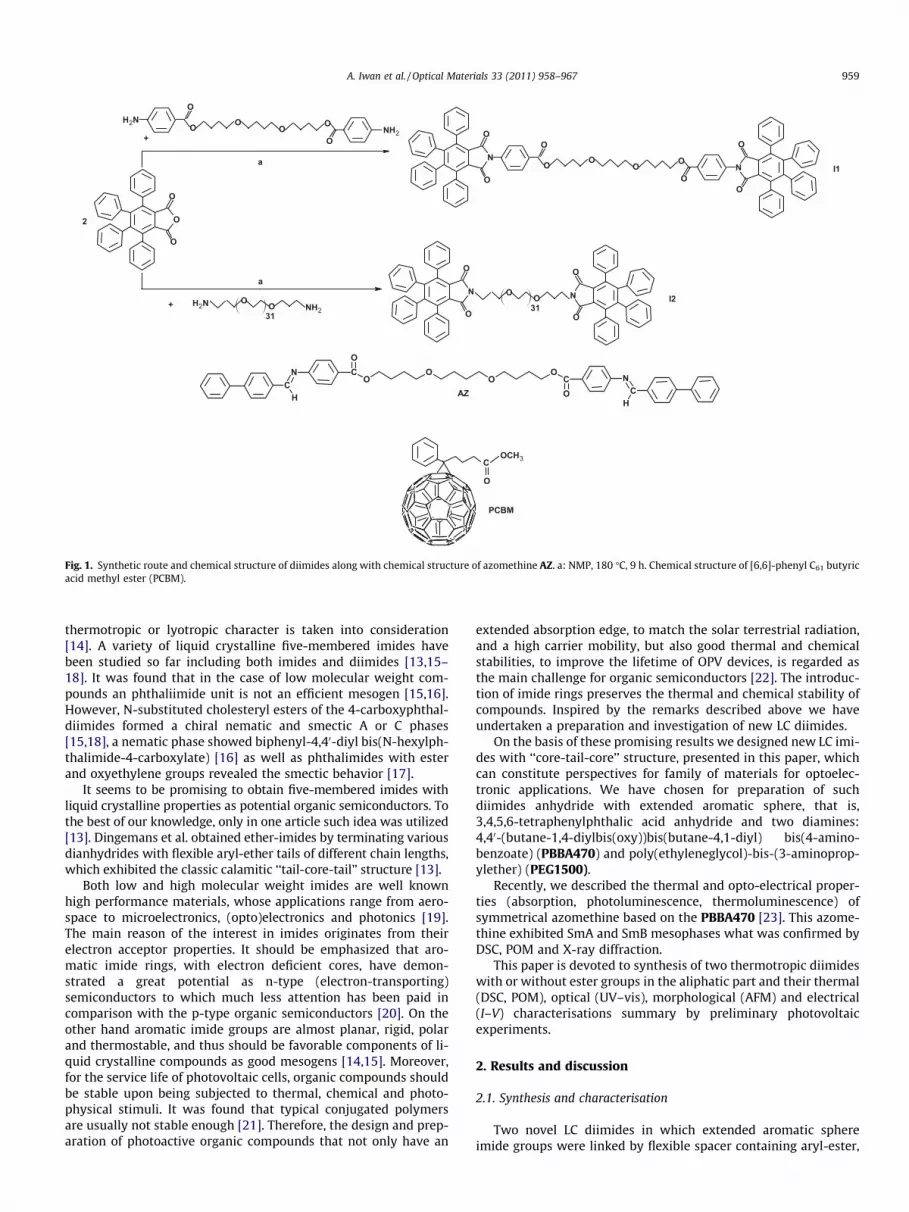
Fig. 1. Synthetic route and chemical structure of diimides along with chemical structure of azomethine AZ. a: NMP, 180 �C, 9 h. Chemical structure of [6,6]-phenyl C61 butyricacid methyl ester (PCBM).
A. Iwan et al. / Optical Materials 33 (2011) 958–967 959
thermotropic or lyotropic character is taken into consideration[14]. A variety of liquid crystalline five-membered imides havebeen studied so far including both imides and diimides [13,15–18]. It was found that in the case of low molecular weight com-pounds an phthaliimide unit is not an efficient mesogen [15,16].However, N-substituted cholesteryl esters of the 4-carboxyphthal-diimides formed a chiral nematic and smectic A or C phases[15,18], a nematic phase showed biphenyl-4,40-diyl bis(N-hexylph-thalimide-4-carboxylate) [16] as well as phthalimides with esterand oxyethylene groups revealed the smectic behavior [17].
It seems to be promising to obtain five-membered imides withliquid crystalline properties as potential organic semiconductors. Tothe best of our knowledge, only in one article such idea was utilized[13]. Dingemans et al. obtained ether-imides by terminating variousdianhydrides with flexible aryl-ether tails of different chain lengths,which exhibited the classic calamitic ‘‘tail-core-tail’’ structure [13].
Both low and high molecular weight imides are well knownhigh performance materials, whose applications range from aero-space to microelectronics, (opto)electronics and photonics [19].The main reason of the interest in imides originates from theirelectron acceptor properties. It should be emphasized that aro-matic imide rings, with electron deficient cores, have demon-strated a great potential as n-type (electron-transporting)semiconductors to which much less attention has been paid incomparison with the p-type organic semiconductors [20]. On theother hand aromatic imide groups are almost planar, rigid, polarand thermostable, and thus should be favorable components of li-quid crystalline compounds as good mesogens [14,15]. Moreover,for the service life of photovoltaic cells, organic compounds shouldbe stable upon being subjected to thermal, chemical and photo-physical stimuli. It was found that typical conjugated polymersare usually not stable enough [21]. Therefore, the design and prep-aration of photoactive organic compounds that not only have an
extended absorption edge, to match the solar terrestrial radiation,and a high carrier mobility, but also good thermal and chemicalstabilities, to improve the lifetime of OPV devices, is regarded asthe main challenge for organic semiconductors [22]. The introduc-tion of imide rings preserves the thermal and chemical stability ofcompounds. Inspired by the remarks described above we haveundertaken a preparation and investigation of new LC diimides.
On the basis of these promising results we designed new LC imi-des with ‘‘core-tail-core’’ structure, presented in this paper, whichcan constitute perspectives for family of materials for optoelec-tronic applications. We have chosen for preparation of suchdiimides anhydride with extended aromatic sphere, that is,3,4,5,6-tetraphenylphthalic acid anhydride and two diamines:4,40-(butane-1,4-diylbis(oxy))bis(butane-4,1-diyl) bis(4-amino-benzoate) (PBBA470) and poly(ethyleneglycol)-bis-(3-aminoprop-ylether) (PEG1500).
Recently, we described the thermal and opto-electrical proper-ties (absorption, photoluminescence, thermoluminescence) ofsymmetrical azomethine based on the PBBA470 [23]. This azome-thine exhibited SmA and SmB mesophases what was confirmed byDSC, POM and X-ray diffraction.
This paper is devoted to synthesis of two thermotropic diimideswith or without ester groups in the aliphatic part and their thermal(DSC, POM), optical (UV–vis), morphological (AFM) and electrical(I–V) characterisations summary by preliminary photovoltaicexperiments.
2. Results and discussion
2.1. Synthesis and characterisation
Two novel LC diimides in which extended aromatic sphereimide groups were linked by flexible spacer containing aryl-ester,

Table 1Transition temperatures T (�C) and enthalpy changes DH (kJ/mol) (in parentheses)along with entropy changes DS (J/K �mol) (italic) of I1–I2 and AZ detected from DSC.
Code T (DH) (DS) Refs.
I1a 214.7 (0.65) (1.34); 260.6 (0.87) (1.63) Thiswork
I2b 3.8 (�14.08) (�50.84); 21.6 (10.40) (35.30); 39.7 (7.75)(24.77)
Thiswork
AZc 88.9 (�41.49) (�114.59); 126.1 (45.25) (113.34); 149.8(6.96) (16.47)
[21]
a Heating 2 deg/min.b Heating 1.6 deg/min.c Heating 1 deg/min.
960 A. Iwan et al. / Optical Materials 33 (2011) 958–967
and/or ether linkages with aliphatic groups were obtained andcharacterized. Chemical structure of the compounds synthesizedin this research is presented in Fig. 1.
Tetraphenyl phthalic anhydride and 4,40-(butane-1,4-diyl-bis(oxy))bis(butane-4,1-diyl) bis(4-aminobenzoate) (PBBA470)was utilized for preparation of diimide I1 and poly(ethylenegly-col)-bis-(3-aminopropylether) (PEG1500) for I2. Such diamineswere chosen, because, it was found that the presence of both: oxy-ethylene and aryl-ester spacer promotes the LC behavior [16,23].Extended aromatic sphere anhydride seems to be sufficient forobtaining of imide mesogen. First time, tetraphenylphthalic anhy-dride and PBBA470 were applied to synthesis of LC diimides. Tothe best of our knowledge, such anhydride was applied for (i) syn-thesis imide containing perylene core, as bulky peripheral units forthe control of fluorescent dye aggregation in solution [24] and (ii)for preparation of bisphenol containing the 1,2,4-triazole moietywith pendant phthalimide group attached through a NAN linkagebetween tetraphenylphthalic anhydride and an N-amino-1,2,4-triazole [25].
Both compounds showed good solubility in common solventssuch as chloroform, DMA, NMP. The assigned chemical structuresof synthesized diimides I1 and I2 were identified through the datafrom 1H NMR, FTIR spectroscopy measurements and elementalanalysis. The FTIR spectra of the compounds exhibited characteris-tic absorption bands of a five-membered aromatic imide at 1720,1780 (imide C@O stretch); 1344 (CAN stretch); 809 and 745(CAH bend) and 2917 and 2849 (aliphatic CAH stretch) cm�1.The 1H NMR spectra showed signals for the protons of the aromaticrings at 8.04–6.73 ppm in the case of I1 and 7.26–6.75 ppm in I-2spectrum. In 1H NMR spectrum of I1 signals at 4.32–4.31 ppmcharacteristic for AC(O)OACH2A, at 3.45–3.41 ppm for AOACH2Aand at 1.83–1.61 ppm for CH2 were observed. 1H NMR spectrum ofI2 exhibited signals for the protons of NACH2A at 3.64 ppm,AOACH2A at 3.47 ppm and CH2 at 1.87–1.80 ppm.
2.2. Thermal properties
In order to investigate the mesomorphic behavior of diimideswe performed differential scanning calorimetry (DSC) experimentsunder nitrogen atmosphere using different heating and coolingrates in a temperature range from �60 �C to over the clearingpoint. Both compounds exhibited liquid crystalline properties.The transition temperatures and enthalpies of the diimides I1–I2determined by DSC are presented in Table 1.
DSC studies revealed that the imide I1 exhibited a clearing pointtemperature higher than 255 �C, while compound I2 showed iso-tropisation higher than 39 �C and broad thermal range of the meso-phase (Table 1). DSC thermograms of the diimides I1, I2 andazomethine AZ are shown in Fig. 2.
Phase behavior of both compounds was investigated addition-ally by polarized optical microscopy. Both compounds formedtwo stable smectic (Sm) mesophases. Photomicrographs of the
optical textures of mesophases obtained for the I1 and I2 are pre-sented in Fig. 3. The differences in the isotropisation temperatureof investigated imides were observed. This behavior showed therole of the diamine structure in creating their mesomorphic prop-erties of diimides.
In previous work [23] the authors investigated azomethine AZobtained from PBBA470 and it is seem to be interesting to comparethe mesomorphic properties of the diimide I1 and azomethine AZ.Therefore, the structure of the azomethine AZ is presented in Fig. 1.Being into consideration the temperature of isotropisation the fol-lowing scenario was observed: 255 �C (I1) > 150 �C (AZ) > 59 �C(I2). It was surprise that introduction the azomethine bonds as inAZ influenced on huge decrease (105 �C) of the temperature of iso-tropisation in comparison with diimide (I1). Contrary, the presenceof poly(ethyleneglycol)-bis-(3-aminopropylether) as in the case ofI2 influences on the decrease of the isotropisation temperature(compare I2 and I1 or I2 and AZ). This behavior suggested thatmesomorphic properties of the investigated compounds dependon the kind of aliphatic part and kind of the bond (imide or imine).Thermal parameters of diimides and azomethine AZ are presentedin Table 1.
It is know, that all observed phase transitions can be quantita-tively analyzed basing on their entropy (DS) values. However, thisvalue is not widely investigated in the papers [26,27]. Conse-quently entropy changes (DS) of phase transitions were calculatedby using following formula:
DS ¼ DH=T
where enthalpy DH and temperature T of phase transitions were ta-ken from the DSC calorimetry. All measurements were performedby using the identical calorimetric setup.
In our case the highest value of entropy exhibited azomethineAZ (Table 1). On the other hand along with increase of the lengthof the aliphatic part as it is in I2, the increase of entropy valueswas observed in comparison with I1.
Parameters of heating and cooling process of I1 and AZ were sim-ilar. Diimide I1 and azomethine AZ exhibited reversible thermalbehavior as determined by DSC and POM experiments. CompoundAZ showed a liquid crystal to isotropic transition at 149.8 �C with aDH = 8.7 J/g on the heating rate 1 deg/min (Fig. 2b). On cooling fromthe isotropic state to room temperature, an exothermic peak ap-peared at 147.2 �C with a DH = 8.9 J/g, corresponding to the transi-tion from the isotropic state to the liquid crystalline phase(Fig. 2b). Moreover, it should be note that during heating of the sam-ple (after rapid cooling) so called ‘‘cold’’ crystallization was observedat 88.9 �C (Fig. 2b). Compound I2 also exhibited ‘‘cold’’ crystalliza-tion at 3.8 �C (Fig. 2a) during heating of the sample. Moreover,diimide I2 during cooling of the sample was organized very slowly.Compound I1 showed a liquid crystal to isotropic transition at260.6 �C on the heating rate 2 deg/min. On cooling from the isotropicstate to room temperature, an exothermic peak appeared at 255.5 �C(DH = 0.7 J/g), corresponding to the transition from the isotropicstate to the liquid crystalline phase. Additionally, during cooling ofthe I1 second exothermic peak at 155.4 �C with DH = 0.7 J/g wasfound.
The compounds I1 and I2 were investigated by DSC during dif-ferent heating and cooling cycles. DSC traces of the I1 during cool-ing at 0.9 deg/min showed two peaks with maxima at 116.2 �C and200.5 �C with DH = 3.4 J/g and 2.4 J/g, respectively. During heatingof the I1 at 0.9 deg/min also two peaks at 109.3 �C and 260.1 �Cwith DH = 1.7 J/g and 1.1 J/g, respectively was found.
DSC traces of the I2 during heating of the sample at 0.5 deg/minshowed two peaks at 29.4 �C and 41.1 �C, with the value of enthal-py DH = 0.5 J/g and 0.4 J/g, respectively. During heating of the I2 at0.3 deg/min also two peaks at 31.4 �C and 41.4 �C with DH = 0.4 J/gand 0.5 J/g, respectively was found. DSC traces of the I2 during
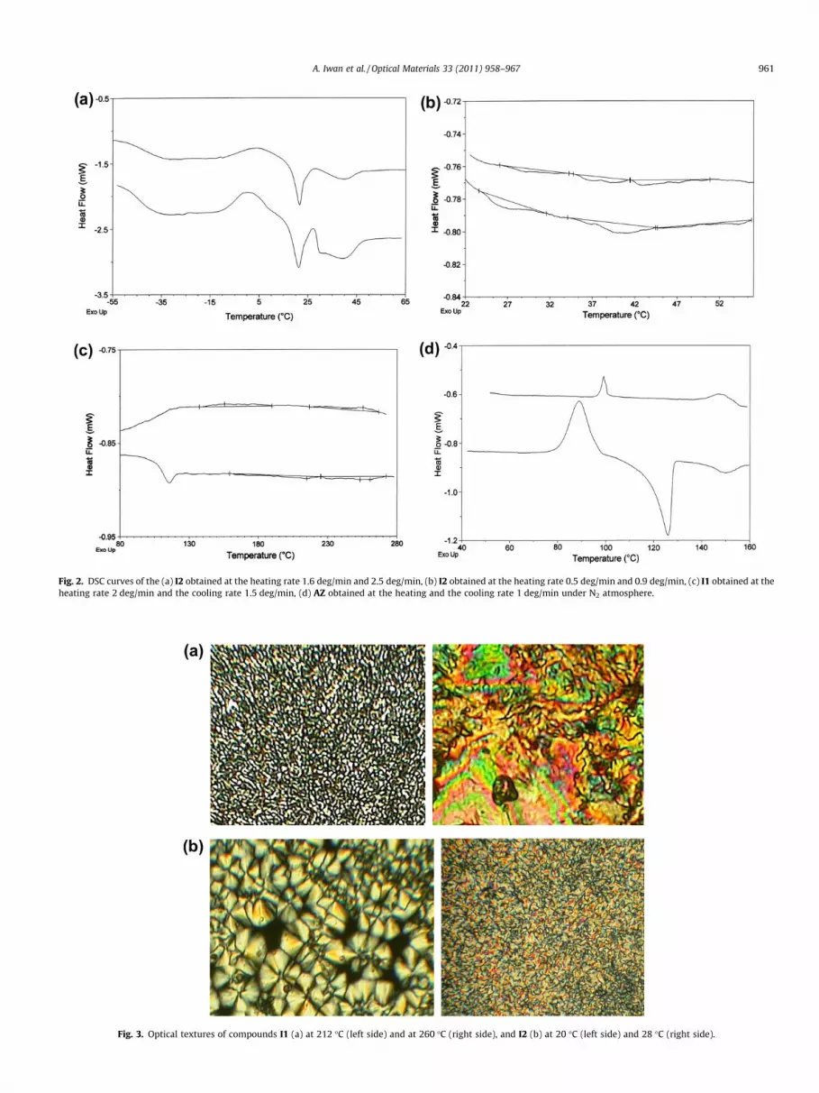
Fig. 2. DSC curves of the (a) I2 obtained at the heating rate 1.6 deg/min and 2.5 deg/min, (b) I2 obtained at the heating rate 0.5 deg/min and 0.9 deg/min, (c) I1 obtained at theheating rate 2 deg/min and the cooling rate 1.5 deg/min, (d) AZ obtained at the heating and the cooling rate 1 deg/min under N2 atmosphere.
Fig. 3. Optical textures of compounds I1 (a) at 212 �C (left side) and at 260 �C (right side), and I2 (b) at 20 �C (left side) and 28 �C (right side).
A. Iwan et al. / Optical Materials 33 (2011) 958–967 961

Fig. 4. AFM images of the following diimides (from the top): I1–I2 and AZ, respectively. Topography (left) processed with Inclination transformation (central) and the PhaseImaging (right) are presented.
Table 2The surface parameters of I1 and I2 and for comparison for AZ.
Code Surface statisticsa Refs.
Ra (nm) Rms (nm) Skew Kurtosis Surface area ratio
I1 0.65 0.88 1.33 7.01 1.0004 This workI2 145.3 180.4 0.57 �0.42 1.0129 This workAZ 36.20 50.00 1.59 2.08 1.1333 [21]
a Values calculated for scanning field 10 lm � 10 lm (100 lm2 scan area).
962 A. Iwan et al. / Optical Materials 33 (2011) 958–967
cooling at 0.3 deg/min showed two peaks with maxima at 32.3 �Cand 41.9 �C with DH = 0.2 J/g and 0.3 J/g, respectively.
2.3. AFM study
In our experiments we investigated the influences of the chem-ical structure of the imides on the surface morphology of the mate-rials. Films on the glass substrates were obtained by dissolving atroom temperature the compound in chloroform to form a homog-enous solution. Residual solvent was removed by heating of thefilm. Fig. 4 shows an AFM images obtained for both compounds.
Films of the imides obtained by casting from chloroform solutionshow a very interesting morphology, characteristic for systemscapable of forming organized supramolecular structures in linearstructure of the compounds with different type of sub-unit. AFMimages of the I1–I2 presented typical, planar view of the topographyas well as Inclination transformation, which we use to provide a bet-ter view of fine structures and features. Also Phase Image was placed,which shows maps of viscoelastic forces, useful for imaging inhomo-geneous materials (Fig. 4). Surface of I1 sample showed no particularfeatures related to its macromolecular structure. However, I2 re-vealed highly ordered, 5 nm thick step-like structures.

Table 3Summary of UV–vis experiments of I1 and I2 in films on the quartz slides.
Code kmax (nm) Eopt:g (eV) Er¼2
g (eV) Er¼0:5g (eV)
I1 264, 335 3.15 3.04 3.31I2 226, 323 3.11 2.90 3.35
A. Iwan et al. / Optical Materials 33 (2011) 958–967 963
As we reported in [23] the film of AZ showed ordered, planar-oriented morphology (see Fig. 4). AFM images of AZ, revealedterraces-like organizational features as we could clear see in theInclination transformation. The AZ exhibited layered structure [23].
When the topography is measured, one can determine certaindata describing the properties of the surface. Typical parameteris roughness (Ra, Rms). However, more practical is to use otherparameters named skew (the unbalance of height distributionmaximum) and kurtosis (the peak’s width on height distribution).Mentioned parameters, measured for two investigated surface arepresented in Table 2.
2.4. UV–vis spectra
UV–vis spectra of the diimides were measured for thin film onthe quartz substrate. Thin films were prepared from chloroformsolution of compounds (11 mg of I1 and 15 mg of I2 were dissolvedin 1 mL of chloroform). The solutions were spread on quartz glassusing spin-coating method. Quartz substrates were purified usingsuch organic solvents as chloroform and acetone. Characteristicparameters related with speed (880 turn per minute) and time(10 s) of rotation were applied to spin-coating equipment.
All parameters (transmission, reflectivity, film thickness) whichare necessary to calculate absorption coefficient (a) were mea-sured using spectrophotometer JASCO V670 and original programsconnected with this apparatus. Calculation of layer thickness (d)was made in UV/Vis range from reflectance measurements(dI1 = 200 nm and dI2 = 200 nm). The scattering phenomenon wastaken into consideration.
UV–vis parameters of the diimides are presented in Table 3 andFig. 5.
Energy band gap was calculated from absorption spectrum(abbreviation Eopt:
g ) and additionally from absorption coefficient(a) (abbreviation Er¼0:5
g and Er¼2g ). Absorption coefficient was calcu-
lated from reflectivity and transmission using the following equa-tion [28,29].
a ¼ 1d
lnð1� RÞ2
T
!ð1Þ
where T is the transmission, R the reflectivity, d is the film thickness.Eq. (1) represents absorption coefficient as a function of reflec-
tivity, transmission and thickness of layer. Absorption coefficientplots of the I1 and I2 thin layers are presented in Fig. 5b.
To delimitated energy band gaps following equations wereapplied:
Eg ¼ 1240=k ð2Þ
a � E ¼ AðE� EgÞr ð3Þ
where a is the absorption coefficient, A the parameter independentfrom photon energy, E the photon energy, Eg the energy band gap, ris the index corresponds with band to band transition.
The energy band gap of investigated diimides was calculated forindex r equal to 0.5 and 2, which correspond to direct (r = 0.5) andindirect (r = 2) band to band transition.
Linear approximation of absorption edge was obtained from thebelow equation:
ðaEÞ1r ¼ f ðEÞ ð4Þ
Linear approximations of absorption edge of the diimides thin lay-ers on quartz are shown in Fig. 5c.
Differences between value of energy band gap derived fromabsorption spectrum and calculated from absorption coefficientare presented in Table 3. Value of energy band gap of I1 and I2 de-tected from absorption spectrum (Eopt:
g ) was lower than the value of(Eðr¼0:5Þ
g , calculated from Eq. (3). However, Eopt:g was higher than the
(Eðr¼2Þg , calculated from Eq. (3) for r = 2. The Eopt:
g values detectedfrom absorption spectra for both diimides were similar. Analogousobservation was detected for energy band gap calculated fromabsorption coefficient (see Table 3). Differences between value ofenergy band gap obtained from absorption spectrum and calcu-lated form absorption coefficient were small and were in the rangeof 0.11–0.24 eV.
The UV–vis spectra of the diimides in the solid state as thin filmprovided evidence confirming their molecular structures. Bothcompounds exhibited two well defined absorption bands, first inthe range of 226–264 nm and the second one in the range of323–335 nm, being responsible for p–p� transition (see Table 3and Fig. 5).
Additionally, the effect of incorporation of PBBA470 or PEG1500into the compound backbone, on the optical properties was tested.For example, the presence of PBBA470 group in I1 results in a bath-ochromic shift of both absorption bands in comparison with I2. Onthe other hand, azomethine AZ which contains PBBA470 exhibitedtwo absorption maxima at 230 and 311 nm. Both absorption bandsof AZ were blue shifted in comparison with I1. This behavior clearlyshowed influence of imide and imine bond on absorption propertiesin UV–vis range of investigated compounds.
2.5. Current–voltage measurements
Devices with the following architecture: ITO/compound/Al, ITO/compound:PCBM/Al and ITO/PEDOT:PSS/compound:PCBM/Al wereconstructed. Firstly, current–voltage (I–V) measurements of I2 per-formed on ITO/I2/Al device before and after irradiation with light(halogen lamp, about 1000 W/m2) was investigated. From obtainedresults it was possible to calculate a luminal voltage for illumi-nated and dark measurements. Differences between device ITO/I2/Al illuminated and not illuminated were observed. For example,the turn-on voltage of the device ITO/I2/Al was observed at about0.5 V in room temperature under 1000 W/m2 and in dark condi-tions it was observed at about 1.0 V in room temperature. As anexample, current–voltage curves of ITO/I2/Al before and underirradiation are shown in Fig. 6a.
Differences were found along with change of the device structure.It can be seen that for the device ITO/I2:PCBM/Al the turn-on voltagewas observed at about 2.0 V in room temperature without and underillumination 1000 W/m2. Opposite behavior was observed for thedevice with such construction as ITO/I1:PCBM/Al. For this devicethe turn-on voltage was observed at about 3.0 V in room tempera-ture without illumination and at about 1.5 V under illumination1000 W/m2. Current–voltage curves of ITO/I2:PCBM/Al and ITO/I1:PCBM/Al before and after irradiation are shown in Fig. 6b and c.
Additionally, we investigated also influence of PEDOT:PSS layerfor current–voltage characteristic of such device as ITO/PEDOT:PSS/I2:PCBM/Al. Differences between device illuminated and noilluminated were observed. For example, for the device ITO/PEDOT:PSS/I2:PCBM/Al under illumination 1000 W/m2 the turn-onvoltage was observed at about 8.0 V in room temperature, whilefor the same device without illumination was found about 3 V(Fig. 6d). This behavior confirmed the influence of the azometinestructure, fullerenes and PEDOT:PSS on the I–V characteristic ofthe polymers. The differences found in the I–V characteristic of

200 250 300 350 400 450 500 550 600 650 700 750 800Wawenumber [nm]
Abs
orba
nce
(a.u
.)
I1 I2
1,75 2,00 2,25 2,50 2,75 3,00 3,25 3,50 3,75 4,00 4,25 4,50 4,750,0
2,0x10⁴
4,0x10⁴
6,0x10⁴
8,0x10⁴
1,0x10⁵
1,2x10⁵
1,4x10⁵
α (c
m-1)
Energy [eV]
I1 I2
2.50 2.75 3.00 3.25 3.50 3.75 4.00 4.25 4.50 4.750
100
200
300
400
500
600
700
800
Energy [eV]
( αE)
1/2 [
(eV/
cm)1/
2 ]
I1 I2
3,00 3,15 3,30 3,45 3,60 3,75 3,90 4,05 4,200,0
3,0x10⁹
6,0x10⁹
9,0x10⁹
1,2x10¹⁰
1,5x10¹⁰
1,8x10¹⁰
2,1x10¹⁰
2,4x10¹⁰
I1 I2
Energy [eV]
(αE)
2 [(e
V/cm
)2 ]
(c)
(b)
(a)
Fig. 5. (a) Room temperature solid-state UV–vis absorption spectra of diimides. Films were spin casted on quartz substrate, (b) absorption coefficient of diimides and (c)linear approximation of absorption edge of diimides for r = 2 (left side) and for r = 0.5 (right side).
964 A. Iwan et al. / Optical Materials 33 (2011) 958–967
the azomethine confirm both the different planarity and conforma-tions of the compound in film.
For devices with active layer diimide:PCBM significant foto-generation of charges (electrons) were found (see Fig. 6). Moreover,it was possible to observe that for the devices ITOncom-pound:PCBMnAl foto-current effect appeared during illuminationthe device (Fig. 5b and c). Additionally, for deviceITOnPEDOT:PSSnazometine:PCBMnAl the same phenomenon wasobserved but at lower value of voltage and also in this case valueof current was higher than in the case of device without PEDOT:PSSlayer. On the other hand it was not possible observed foto-currenteffect in device ITO/compound/Al.
Additionally in Fig. 7 are shown current density–voltage (J–V)characteristics of devices before and after irradiation under1000 W/m2.
Both characteristics it means I–V and J–V of all devices weresimilar.
2.6. Photovoltaic measurements
Preliminary series of I–V characteristics were taken for eachtype of investigated cell structure. Basing on these results open cir-cuit voltage VOC and short circuit current JSC were obtained. Theranges of measurements were adjusted experimentally for each

0,0 0,5 1,0 1,5 2,0 2,5 3,0 3,5 4,0 4,5 5,00
20
40
60
80
100
120
140
160
180
200
ITO\I2\Al dark illumination
I [µA
]
U [V]0,0 0,8 1,6 2,4 3,2 4,0 4,8 5,6 6,4 7,2
4
6
8
10
12
14
16
18
20
22
24
ITO\I2:PCBM\Al dark illumination
U [V]
I [nA
]
0,0 0,5 1,0 1,5 2,0 2,5 3,0 3,5 4,0
0,0
0,3
0,6
0,9
1,2
1,5
1,8
2,1
2,4
2,7
3,0
3,3
ITO\M11:PCBM(1:1)\Al dark illumination
I [m
A]
U [V]0 1 2 3 4 5 6 7 8 9 10 11 12 13 14 15
0102030405060708090
100110120130140
ITO\PEDOT:PSS\I2:PCBM(1:1)\Al dark illumination
U [V]
I [µ A
]
(b)
(d)(c)
(a)
Fig. 6. Current–voltage curves of (a) ITO/I2/Al, (b) ITO/I2:PCBM/Al, (c) ITO/I1:PCBM/Al and (d) ITO/PEDOT:PSS/I2:PCBM/Al devices before and after irradiation under 1000 W/m2.
Table 4Photovoltaic parameters of ITOnI2nAl, ITOnI2:PCBMnAl, ITOnPEDOT:PSSnI2:PCBMnAl.
Device Jsc (mA/cm2) Voc (mV)
ITOnI2nAl 0.0034 3.01ITOnI2:PCBMnAl 0.54 660ITOnPEDOT:PSSnI2:PCBMnAl 0.56 166
A. Iwan et al. / Optical Materials 33 (2011) 958–967 965
cell and the final outcomes were the mean values of ten measure-ments at each point.
Obtained results confirm the photovoltaic effects in all testedconstructions. Measured efficiencies were very low (below0.00001%). Results are presented in Table 4 and in Fig. 8.
Fullerenes and PEDOT:PSS influences positively on the value of JSC.There are several reasons for such behavior. I2 is not fully conjugatedand we attribute the poor photovoltaic performance to difficulty incharge hopping between monomer units. There are several possibili-ties limiting the JSC of the devices, for example, low photolumines-cence efficiency in the compound film. As one of the obviousreasons of very low value of efficiencies, high series resistance maybe identified. For further experiments several features of the cellsshould be improved. Among them better quality of the ITO and metal-lic contacts is needed for higher test reliability. It is clear that the I2 isprobably not promising material for photovoltaic applications.
3. Conclusion
Two mesogenic diimides based on 3,4,5,6-tetraphenylphthalicacid anhydride were prepared. It was found that the mesophases
depended on aliphatic chain chemical structure. Preliminary inves-tigations of the current–voltage characteristics carried out beforeand after irradiation with light for devices with following structureITO/compound/Al, ITO/compound:PCBM/Al and ITO/PEDOT:PSS/compound:PCBM/Al prepared from obtained diimides, confirmedsemiconductivity properties of the organic thin film. Both diimidescovered the absorption spectrum to about 340 nm and exhibitedcurrent response at low value of voltage. These advantages of dii-mides investigated in this paper together with their mesomorphicbehavior are promising for used them in organic electronics.
4. Experimental
4.1. Materials
All chemicals and reagents were used as received from Aldrich.
4.1.1. Synthesis of the diimidesTetraphenylphthalic anhydride (1 mmol, 0.4525 g) and PABA
470 (0.5 mmol, 0.240 g) for preparation of I1 or poly(ethylenegly-col)-bis-(3-aminopropylether) (PEG-1500) (0.5 mmol, 0.75 g) forI2 were placed in a flask equipped with a nitrogen gas inlet and dis-solved in 2.8 or 4.8 mL of anhydrous N-methyl-pyrrolidone (NMP).The obtained mixture was stirred and headed to 180 �C during 3 hand maintained at that temperature for 6 h. During the heating,water produced by the imidization reaction was removed continu-ously with a stream of nitrogen. The reaction mixture was thencooled to room temperature.

0.0 0.5 1.0 1.5 2.0 2.5 3.0 3.5 4.0 4.5 5.00
1
2
3
4
5
6
7
8
U [V]
J [ µ
A/c
m2 ]
ITO\I2\Al dark illumination
0,0 0,5 1,0 1,5 2,0 2,5 3,0 3,5 4,0 4,5 5,0 5,5 6,0 6,5 7,00,1
0,2
0,3
0,4
0,5
0,6
0,7
0,8
0,9
1,0
J [n
A/c
m2 ]
U [V]
ITO\I2:PCBM\Al dark illumination
0,0 0,5 1,0 1,5 2,0 2,5 3,0 3,5 4,0
0
10
20
30
40
50
60
70
80
90
ITO\I1:PCBM(1:1)\Al dark illumination
J [ µ
A/c
m2 ]
U [V]0 1 2 3 4 5 6 7 8 9 10 11 12 13 14 15
0,0
0,5
1,0
1,5
2,0
2,5
3,0
3,5
4,0
4,5
5,0
5,5
6,0
U [V]
J [µ
A/c
m2 ]
ITO\PEDOT:PSS\I2:PCBM(1:1)\Al dark illumination
(a) (b)
(c) (d)
Fig. 7. Current density–voltage (J–U) curves of (a) ITO/I2/Al, (b) ITO/I2:PCBM/Al, (c) ITO/I1:PCBM/Al and (d) ITO/PEDOT:PSS/I2:PCBM/Al devices before and after irradiationunder 1000 W/m2.
-0,7 -0,6 -0,5 -0,4 -0,3 -0,2 -0,1 0,0 0,1 0,2 0,3 0,4 0,5 0,6 0,7-1,5
-1,2
-0,9
-0,6
-0,3
0,0
0,3
0,6
0,9
1,2
1,5
U [V]
J [m
A/c
m2 ]
Dark ITO\I2Al ITO\I2:PCBM\Al ITO\PEDOT:PSS\I2:PCBM\Al
Fig. 8. J–U characteristics of ITOnI2nAl, ITOnI2:PCBMnAl, ITOnPEDOT:PSSnI2:PCBMnAl.
966 A. Iwan et al. / Optical Materials 33 (2011) 958–967
Compound I1 was precipitated with mixture of methanol:water (1:1), and then was crystallized from methanol with water(1:1) and dried in a vacuum oven. Compound I2 was precipitatedand crystallized with water and dried in a vacuum oven.
I1: FTIR (KBr, cm�1): 2943, 2861 (aliphatic groups), 1778, 1723,1363, 1109, 731 (imide); 1H NMR (300 MHz, CDCl3, TMS) D, ppm:aromatic protons 8.04–8.03 (m, 4H), 7.50–7.49 (m, 4H), 7.25–6.73(m, 40H), 4.32–4.31 (m, 4H, ACOOACH2A), 3.45–3.41 (m, 8H,AOACH2A), 1.83–1.61 (m, 12H, ACH2ACH2ACH2A). 13C NMR(75 MHz, CDCl3, TMS) d, ppm: 25.56, 25.67, 26.28, 26.38, 26.45,
64.16, 64.99, 70.13, 70.26, 70.56, 70.65, 113.75, 126.05, 126.40,126.71, 127.03, 127.17, 127.37, 127.47, 127.52, 127.61, 127.90,129.70, 129.81, 129.93, 130.48, 130.66, 131.52, 134.38, 135.41,137.29, 137.83, 140.02, 141.35, 148.52, 149.97, 161.62, 165.77. Anal.Calcd. for (C90H72N2O10)n (1341.53): C 78.67, H 5.31, N 2.04; Found C78.69, H 5.15, N 1.70.
I2: FTIR (KBr, cm�1): 2873 (aliphatic groups), 1768, 1711, 1366,1106, 698 (imide); 1H NMR (300 MHz, CDCl3, TMS) d, ppm: aromaticprotons 7.26–6.75 (m, 40H), 3.64 (m, 4H, NACH2ACH2A), 3.47 (m,128H, ACH2AOA), 1.87–1.80 (m, 4H, ACH2ACH2ACH2A). 13C NMR(75 MHz, CDCl3, TMS) d, ppm: 28.49, 35.49, 68.89, 70.12, 70.48,70.53, 126.22, 126.92, 127.22, 127.27, 129.86, 130.72, 135.63,138.03, 139.20, 147.62, 167.19. Anal. Calcd. for (C132H180N2O36)n
(2370.78): C 66.87, H 7.65, N 1.18; Found C 63.13, H 7.04, N 1.86.
4.2. Measurements
Fourier transform infrared (FTIR) spectra were acquired on aBIO-RAD FTS 40 A Spectrometer in transmission mode using KBrpellets. Proton nuclear magnetic resonance (1H NMR) spectra wererecorded on a Bruker AC 300 MHz spectrometer using chloroform(CDCl3) as a solvent and tetramethyl silane (TMS) as an internalstandard. UV–vis absorption spectra were recorded in solid stateas films casted on quartz using spectrophotometer Jasco V670. Dif-ferential scanning calorimetry (DSC) was performed with a TA-DSC2010 apparatus, under nitrogen atmosphere using sealed alumi-num pans. The transition temperatures were read at the top ofthe endothermic and exothermic peaks. The textures of theliquid–crystalline phase were observed with a polarized optical

(a)
(b)
(c)
(d)
Fig. 9. Adaptation of measurement setup for testing of compound one-sidecontacted cells: (a) original measurement table with probes, (b) isolating screenof the base brass contact, (c) polymer bottom-contacted solar cell, (d) additionalemitter contacts for signal transferring.
A. Iwan et al. / Optical Materials 33 (2011) 958–967 967
microscope (POM) Zeiss (Opton-Axioplan) equipped with a NikonCoolpix 4500 color digital camera, and Mettler FP82 hot plate withMettler FP80 temperature controller. Current–voltage characteris-tics were detected using electrometer Keithley 6517B.
The surface morphology investigation of the diimides was per-formed in air using a commercial Innova AFM system from VeecoCompany. Measurements were done in Tapping Mode and PhaseImaging. Also local contrast data processing was made. Typicalcantilever (about 40 N/m and <10 nm tip curvature) was used.
4.3. Device fabrication
Current–voltage measurements were performed on ITO/com-pound/Al, ITOncompound:PCBMnAl and ITOnPEDOT:PSSncom-pound:PCBMnAl. ITO-glass substrates were cleaned in ultrasonicwasher at 15 min in acetone and after that in such organic solventsas isopropanol and acetone. The water solution of PEDOT:PSS(poly(3,4-ethylenedioxythiophene:poly(styrenesulfonate)) layerwas spread on ITO substrate using spin–coating equipment withrotating speed about 3000 turns per minute for 15 s. Thin organiclayers based on azomethine or mixture azometine:PCBM in weightratio 1:1 were dissolved at chloroform and next spread. The activelayers based on azometine or azometine:PCBM (called blend) wasspin-coating onto ITO-covered glass substrate or ITO/PEDOT:PSSsubstrate with angular speed 900 turn per minute by 10 s at roomtemperature. Al electrode (about 28 cm2 area) was prepared on theazomethine film surface by thermal evaporation method at pres-sure of 5 � 10�4 Torr.
4.4. General description of measurement photovoltaic setup
I–V characteristics and parameters were obtained by the help ofintegrated measurement setup, calibrated for STC conditions(AM1,5G, 1000 W/m2 and room temperature 25 �C) according tointernational standards (IEC 60904-1 [30] and IEC 60904-3 [31]).Measurement setup consists of solar simulator equipped with fourxenon bulbs Xenophot HLX and water dispersion filter and dataacquisition system. Solar simulator operates in C+ standard accord-ing to IEC 60904-9 norm [32] at surface of 100 cm2. The light condi-tion is controlled by auto-calibration system equipped withphotocell and on-line regulated impulse power supply. The temper-ature is controlled on-line and may be stabilized by water thermo-stat with accuracy of 0.5 �C.
4.5. Adaptation for polymer solar cells measurements
Towards effective measurements of polymer solar cells theadaptation of I–V tracer was needed. One-side contacting system,shown in Fig. 9, with additional isolation of brass base contactswas elaborated.
Additionally the measurement and simulation model was cali-brated according to expected parameters of polymer device.
Acknowledgements
The authors thank Dr. P. Rannou for gift of anhydride and dia-mines PBBA470 and PEG1500.
References
[1] H. Qu, J. Luo, X. Zhang, Ch. Chi, J. Polym. Sci., Part A Polym. Chem. 48 (2010)186–194.
[2] Q. Zheng, J. Huang, A. Sarjeant, H.E. Katz, J. Am. Chem. Soc. 130 (2008)14410–14411.
[3] J.C. Maunoury, J.R. Howse, M.L. Turner, Adv. Mater. 19 (2007) 805–809.[4] J.B. Bodapati, H. Icil, Dyes Pigm. 79 (2008) 224–235.[5] C.R. Newman, C.D. Frisbie, D.A. da Silna Filio, J.L. Brudas, P.C. Ewbank, K.R.
Mann, Chem. Mater. 16 (2004) 4436–4451.[6] J.G. Laquindanum, H.E. Katz, A. Dodabalapur, A.J. Lovinger, J. Am. Chem. Soc.
118 (1996) 11331–11332.[7] Sh.V. Bhosale, Ch.H. Jani, S.J. Langford, Chem. Soc. Rev. 37 (2008) 331–342.[8] P. Gawrys, D. Boudinet, M. Zagorska, D. Djurado, J.-M. Verilhac, G. Horowitz, J.
Pecaud, S. Pouget, A. Pron, Synth. Met. 159 (2009) 1478–1485.[9] J.Y. Kim, A.J. Bard, Chem. Phys. Lett. 383 (2004) 11–15.
[10] Z. An, J. Yo, B. Domercq, S.C. Jones, S. Barlow, B. Kippelen, S.R. Marder, J. Mater.Chem. 19 (2009) 6688–6698.
[11] A. Wicklein, A. Lang, M. Muth, M. Thelakkat, J. Am. Chem. Soc. 131 (2009)14442–14453.
[12] Z. Wang, C. Kim, A. Facchetti, T.J. Marks, J. Am. Chem. Soc. 129 (2007)13362–13363.
[13] T.J. Dingemans, S.J. Picken, N.S. Murthy, P. Mark, T.L. StClair, E.T. Samulski,Chem. Mater. 16 (2004) 966–974.
[14] H.R. Kricheldorf, V. Linzer, Polymer 36 (1995) 1893–1902.[15] E. Bialecka-Florjanczyk, A. Orzeszko, Liq. Cryst. 15 (1993) 255–258.[16] A. Orzeszko, Macromol. Chem. Phys. 197 (1996) 2461–2465.[17] I. Sledzinska, E. Bialecka-Florjanczyk, A. Orzeszko, Eur. Polym. J. 32 (1996)
1345–1350.[18] E. Bialecka-Florjanczyk, A. Orzeszko, I. Sledzinska, E. Gorecka, J. Mater. Chem. 9
(1999) 371–374.[19] (a) M.K. Gosh, K.L. Mittal, Polyimides: fundamentals and applications, Dekker,
New York, 1996;(b) M. Hasegawa, K. Horie, Prog. Polym. Sci. 26 (2002) 259–335;(c) E. Schab-Balcerzak, M. Siwy, M. Kawalec, A. Sobolewska, A. Chamera, A.Miniewicz, J. Phys. Chem. A 113 (2009) 8765–8780.
[20] J.E. Anthony, A. Facchetti, M. Heeny, S.R. Marder, X. Zhan, Adv. Mater. (2010),doi:10.1002/adma.200903628.
[21] K.M. Coakley, M.D. McGehee, Chem. Mater. 16 (2004) 4533–4542.[22] J.L. Delgado, P.A. Bouit, S. Filippone, M.A. Herranz, N. Martin, Chem. Commun.
46 (2010) 4853–4865.[23] A. Iwan, P. Bilski, H. Janeczek, B. Jarzabek, P. Rannou, A. Sikora, D. Pociecha, B.
Kaczmarczyk, J Mol. Str. 963 (2010) 175–182.[24] H. Langhals, R. Ismael, O. Yürük, Tetrahedron 56 (2000) 5435–5441.[25] A.A.G. Shaikh, A.R. Hlil, P.A. Shaikh, A.S. Hay, Macromolecules 35 (2002)
8728–8737.[26] J. Godzwon, M.J. Sienkowska, Z. Galewski, J. Mol. Str. (2007) 844–845.
259–267.[27] J. Godzwon, M.J. Sienkowska, Z. Galewski, Thermochim. Acta 491 (2009)
71–79.[28] G.I. Rusu, A. Airinei, M. Rusu, P. Prepelit, L. Marin, V. Cozan, I.I. Rusu, Acta
Mater. 55 (2007) 433–442.[29] B. Jarzabek, J. Weszka, A. Burian, G. Pocztowski, Thin Solid Films 279 (1996)
204–208.[30] IEC 60904-1 Photovoltaic devices – Part 1: Measurement of PV current–
voltage characteristics.[31] IEC 60904-3 Photovoltaic devices – Part 3: Measurement principles for
terrestrial photovoltaic (PV) solar devices with reference spectral irradiancedata.
[32] IEC 60904-9 Photovoltaic devices – Part 9: Solar simulator performancerequirements.


![An Experimental Study on the Effect of Substituents on Aromatic-Aromatic Interactions in Dithia[3,3]-metaparacyclophanes](https://img.dokumen.tips/doc/110x75/6352299c85f87b9f8602c92f/an-experimental-study-on-the-effect-of-substituents-on-aromatic-aromatic-interactions.jpg)


