Embed Size (px)
Citation preview
Keysight N9030A PXA Signal AnalyzerThis manual provides documentation for the following instruments:
N9030A Option 503 (3 Hz – 3.6 GHz)
N9030A Option 508 (3 Hz – 8.4 GHz)
N9030A Option 513 (3 Hz – 13.6 GHz)
N9030A Option 526 (3 Hz – 26.5 GHz)
Notice: This document contains references to Agilent. Please note that Agilent’s Test and Measurement business has become Keysight Technologies. For more information, go to www.keysight.com.
Service Guide
N9030A Option 543 (3 Hz – 43 GHz)
N9030A Option 544 (3 Hz – 44 GHz)
N9030A Option 550 (3 Hz – 50 GHz)
Manufacturing Part Number: N9030-90030
NoticeThe information contained in this document is subject to change without notice.
Agilent Technologies makes no warranty of any kind with regard to this material, including but not limited to, the implied warranties of merchantability and fitness for a particular purpose. Agilent Technologies shall not be liable for errors contained herein or for incidental or consequential damages in connection with the furnishing, performance, or use of this material.
Safety InformationThe following safety notes are used throughout this manual. Familiarize yourself with each of the notes and it’s meaning before operating this instrument.
WARNING Warning denotes a hazard. It calls attention to a procedure which, if not correctly performed or adhered to, could result in injury or loss of life. Do not proceed beyond a warning note until the indicated conditions are fully understood and met.
CAUTION Caution denotes a hazard. It calls attention to a procedure that, if not correctly performed or adhered to, could result in damage to or destruction of the instrument. Do not proceed beyond a caution sign until the indicated conditions are fully understood and met.
WARNING This is a Safety Class 1 Product (provided with a protective earthing ground incorporated in the power cord). The mains plug shall only be inserted in a socket outlet provided with a protected earth contact. Any interruption of the protective conductor inside or outside of the product is likely to make the product dangerous. Intentional interruption is prohibited.
Supersedes: February 2012
Printed in USA
August 2014
© Copyright 2011 - 2014 Keysight Technologies, Inc.
2
WARNING The power cord is connected to internal capacitors that may remain live for 5 seconds after disconnecting the plug from it’s power supply.
WARNING The detachable power cord is the instrument disconnecting device. It disconnects the mains circuits from the mains supply before other parts of the instrument. The front panel switch is only a standby switch and is not a LINE switch (disconnecting device).
WARNING The opening of covers or removal of parts is likely to expose dangerous voltages. Disconnect the product from all voltage sources before starting to open.
WARNING These servicing instructions are for use by qualified personnel only. To avoid electrical shock, do not perform any servicing unless you are qualified to do so.
Lithium Battery DisposalThe X-Series Signal Analyzer uses an internal 3.0 VDC battery that contains Lithium/Manganese Dioxide (Li/MnO2). The battery is located on the A4 CPU assembly to power the instrument clock and back up data in SRAM. When the battery is exhausted and ready for disposal, dispose of it according to your country’s requirements. The Agilent part number is 1420-0356 (CR2032). The manufacturer’s part number is CR2032. You can return the battery to your nearest Agilent Technologies Sales and Service office for disposal, if required. Refer to “Contacting Agilent Technologies” on page 41 for a list of Agilent Technologies Sales and Service offices.
3
WarrantyThis Agilent Technologies instrument product is warranted against defects in material and workmanship for a period of one year from date of shipment. During the warranty period, Agilent Technologies Company will, at its option, either repair or replace products which prove to be defective.
For warranty service or repair, this product must be returned to a service facility designated by Agilent Technologies. Buyer shall prepay shipping charges to Agilent Technologies and Agilent Technologies shall pay shipping charges to return the product to Buyer. However, Buyer shall pay all shipping charges, duties, and taxes for products returned to Agilent Technologies from another country.
Agilent Technologies warrants that its software and firmware designated by Agilent Technologies for use with an instrument will execute its programming instructions when properly installed on that instrument. Agilent Technologies does not warrant that the operation of the instrument, or software, or firmware will be uninterrupted or error-free.
LIMITATION OF WARRANTYThe foregoing warranty shall not apply to defects resulting from improper or inadequate maintenance by Buyer, Buyer-supplied software or interfacing, unauthorized modification or misuse, operation outside of the environmental specifications for the product, or improper site preparation or maintenance.
NO OTHER WARRANTY IS EXPRESSED OR IMPLIED. AGILENT TECHNOLOGIES SPECIFICALLY DISCLAIMS THE IMPLIED WARRANTIES OF MERCHANTABILITY AND FITNESS FOR A PARTICULAR PURPOSE.
EXCLUSIVE REMEDIESTHE REMEDIES PROVIDED HEREIN ARE BUYER’S SOLE AND EXCLUSIVE REMEDIES. AGILENT TECHNOLOGIES SHALL NOT BE LIABLE FOR ANY DIRECT, INDIRECT, SPECIAL, INCIDENTAL, OR CONSEQUENTIAL DAMAGES, WHETHER BASED ON CONTRACT, TORT, OR ANY OTHER LEGAL THEORY.
4
Is your product software up-to-date?Periodically, Agilent releases software updates to fix known defects and incorporate product enhancements. To search for software updates for your product, go to the Agilent Technical Support website at:
www.agilent.com/find/techsupport
Trademark AcknowledgementsMicrosoft ® is a U.S. registered trademark of Microsoft Corporation.
Windows ® and MS Windows ® are U.S. registered trademarks of Microsoft Corporation.
Adobe Reader ® is a U.S. registered trademark of Adobe System Incorporated.
Java™ is a U.S. trademark of Sun Microsystems, Inc.
MATLAB ® is a U.S. registered trademark of Math Works, Inc.
Norton Ghost™ is a U.S. trademark of Symantec Corporation.
5

6
Contents
1. OverviewWhat You Will Find in This Chapter . . . . . . . . . . . . . . . . . . . . . . . . . . . . . . . . . . . . . . . . . . . . . . . . . . . . . . 16Agilent PXA Signal Analyzer Overview . . . . . . . . . . . . . . . . . . . . . . . . . . . . . . . . . . . . . . . . . . . . . . . . . . . 17
Virus Information . . . . . . . . . . . . . . . . . . . . . . . . . . . . . . . . . . . . . . . . . . . . . . . . . . . . . . . . . . . . . . . . . . . 17Instrument Option Descriptions . . . . . . . . . . . . . . . . . . . . . . . . . . . . . . . . . . . . . . . . . . . . . . . . . . . . . . . . . . 18Signal Analyzer Accessories . . . . . . . . . . . . . . . . . . . . . . . . . . . . . . . . . . . . . . . . . . . . . . . . . . . . . . . . . . . . 20
Manual Set on CD-ROM . . . . . . . . . . . . . . . . . . . . . . . . . . . . . . . . . . . . . . . . . . . . . . . . . . . . . . . . . . . . . 2050 Ohm Load. . . . . . . . . . . . . . . . . . . . . . . . . . . . . . . . . . . . . . . . . . . . . . . . . . . . . . . . . . . . . . . . . . . . . . . 2150 Ohm/75 Ohm Minimum Loss Pad . . . . . . . . . . . . . . . . . . . . . . . . . . . . . . . . . . . . . . . . . . . . . . . . . . . 2175 Ohm Matching Transformer . . . . . . . . . . . . . . . . . . . . . . . . . . . . . . . . . . . . . . . . . . . . . . . . . . . . . . . . 21AC Probe . . . . . . . . . . . . . . . . . . . . . . . . . . . . . . . . . . . . . . . . . . . . . . . . . . . . . . . . . . . . . . . . . . . . . . . . . 21AC Probe (Low Frequency) . . . . . . . . . . . . . . . . . . . . . . . . . . . . . . . . . . . . . . . . . . . . . . . . . . . . . . . . . . . 21Broadband Preamplifiers and Power Amplifiers . . . . . . . . . . . . . . . . . . . . . . . . . . . . . . . . . . . . . . . . . . . 22RF and Transient Limiters . . . . . . . . . . . . . . . . . . . . . . . . . . . . . . . . . . . . . . . . . . . . . . . . . . . . . . . . . . . . 22Power Splitters . . . . . . . . . . . . . . . . . . . . . . . . . . . . . . . . . . . . . . . . . . . . . . . . . . . . . . . . . . . . . . . . . . . . . 22Static Safe Accessories . . . . . . . . . . . . . . . . . . . . . . . . . . . . . . . . . . . . . . . . . . . . . . . . . . . . . . . . . . . . . . . 22
Before You Start Troubleshooting . . . . . . . . . . . . . . . . . . . . . . . . . . . . . . . . . . . . . . . . . . . . . . . . . . . . . . . . 23ESD Information. . . . . . . . . . . . . . . . . . . . . . . . . . . . . . . . . . . . . . . . . . . . . . . . . . . . . . . . . . . . . . . . . . . . . . 25
Protection from Electrostatic Discharge . . . . . . . . . . . . . . . . . . . . . . . . . . . . . . . . . . . . . . . . . . . . . . . . . . 25Handling of Electronic Components and ESD . . . . . . . . . . . . . . . . . . . . . . . . . . . . . . . . . . . . . . . . . . . . . 26Test Equipment Usage and ESD . . . . . . . . . . . . . . . . . . . . . . . . . . . . . . . . . . . . . . . . . . . . . . . . . . . . . . . . 26For Additional Information about ESD. . . . . . . . . . . . . . . . . . . . . . . . . . . . . . . . . . . . . . . . . . . . . . . . . . . 26
Service Equipment You Will Need . . . . . . . . . . . . . . . . . . . . . . . . . . . . . . . . . . . . . . . . . . . . . . . . . . . . . . . 27Tools you will need . . . . . . . . . . . . . . . . . . . . . . . . . . . . . . . . . . . . . . . . . . . . . . . . . . . . . . . . . . . . . . . . . . 27Calibration Application Software . . . . . . . . . . . . . . . . . . . . . . . . . . . . . . . . . . . . . . . . . . . . . . . . . . . . . . . 27Front End Controller Troubleshooting Kit . . . . . . . . . . . . . . . . . . . . . . . . . . . . . . . . . . . . . . . . . . . . . . . . 28USB Keyboard and Mouse . . . . . . . . . . . . . . . . . . . . . . . . . . . . . . . . . . . . . . . . . . . . . . . . . . . . . . . . . . . . 29USB Storage Device . . . . . . . . . . . . . . . . . . . . . . . . . . . . . . . . . . . . . . . . . . . . . . . . . . . . . . . . . . . . . . . . . 29Required Test Equipment List. . . . . . . . . . . . . . . . . . . . . . . . . . . . . . . . . . . . . . . . . . . . . . . . . . . . . . . . . . 30
After an Instrument Repair . . . . . . . . . . . . . . . . . . . . . . . . . . . . . . . . . . . . . . . . . . . . . . . . . . . . . . . . . . . . . . 40Contacting Agilent Technologies . . . . . . . . . . . . . . . . . . . . . . . . . . . . . . . . . . . . . . . . . . . . . . . . . . . . . . . . . 41
Instrument Serial Numbers . . . . . . . . . . . . . . . . . . . . . . . . . . . . . . . . . . . . . . . . . . . . . . . . . . . . . . . . . . . . 43How to Return Your Instrument for Service. . . . . . . . . . . . . . . . . . . . . . . . . . . . . . . . . . . . . . . . . . . . . . . . . 44
Service Order Number . . . . . . . . . . . . . . . . . . . . . . . . . . . . . . . . . . . . . . . . . . . . . . . . . . . . . . . . . . . . . . . 44Original Packaging . . . . . . . . . . . . . . . . . . . . . . . . . . . . . . . . . . . . . . . . . . . . . . . . . . . . . . . . . . . . . . . . . . 44Other Packaging . . . . . . . . . . . . . . . . . . . . . . . . . . . . . . . . . . . . . . . . . . . . . . . . . . . . . . . . . . . . . . . . . . . . 45
2. Boot Up and Initialization TroubleshootingWhat You Will Find in This Chapter . . . . . . . . . . . . . . . . . . . . . . . . . . . . . . . . . . . . . . . . . . . . . . . . . . . . . . 48Check the Basics . . . . . . . . . . . . . . . . . . . . . . . . . . . . . . . . . . . . . . . . . . . . . . . . . . . . . . . . . . . . . . . . . . . . . . 49PXA Instrument Boot Up Process . . . . . . . . . . . . . . . . . . . . . . . . . . . . . . . . . . . . . . . . . . . . . . . . . . . . . . . . 50
Typical instrument boot-up process flow . . . . . . . . . . . . . . . . . . . . . . . . . . . . . . . . . . . . . . . . . . . . . . . . . 51Potential Problems During Boot Process . . . . . . . . . . . . . . . . . . . . . . . . . . . . . . . . . . . . . . . . . . . . . . . . . . . 54
Yellow Standby LED Does Not Illuminate . . . . . . . . . . . . . . . . . . . . . . . . . . . . . . . . . . . . . . . . . . . . . . . . 54Green Power On LED Does Not Illuminate . . . . . . . . . . . . . . . . . . . . . . . . . . . . . . . . . . . . . . . . . . . . . . . 56Fan(s) Are Not Operating . . . . . . . . . . . . . . . . . . . . . . . . . . . . . . . . . . . . . . . . . . . . . . . . . . . . . . . . . . . . . 60No Agilent Splash Screen Displayed . . . . . . . . . . . . . . . . . . . . . . . . . . . . . . . . . . . . . . . . . . . . . . . . . . . . 62Instrument Hangs at the Agilent Splash Screen . . . . . . . . . . . . . . . . . . . . . . . . . . . . . . . . . . . . . . . . . . . . 64Instrument Cannot Completely Load or Run the Operating System . . . . . . . . . . . . . . . . . . . . . . . . . . . . 65
7
Contents
Troubleshooting a Blank Display . . . . . . . . . . . . . . . . . . . . . . . . . . . . . . . . . . . . . . . . . . . . . . . . . . . . . . . 65Verify LCD Backlight Functionality. . . . . . . . . . . . . . . . . . . . . . . . . . . . . . . . . . . . . . . . . . . . . . . . . . . . . 66Verify Video Signal Path Integrity . . . . . . . . . . . . . . . . . . . . . . . . . . . . . . . . . . . . . . . . . . . . . . . . . . . . . . 69Video Controller / LCD Troubleshooting . . . . . . . . . . . . . . . . . . . . . . . . . . . . . . . . . . . . . . . . . . . . . . . . . 69Initializations Did Not Complete . . . . . . . . . . . . . . . . . . . . . . . . . . . . . . . . . . . . . . . . . . . . . . . . . . . . . . . 69Fails an Initial Alignment . . . . . . . . . . . . . . . . . . . . . . . . . . . . . . . . . . . . . . . . . . . . . . . . . . . . . . . . . . . . . 70
Signal Level Verification . . . . . . . . . . . . . . . . . . . . . . . . . . . . . . . . . . . . . . . . . . . . . . . . . . . . . . . . . . . . . . . 76Signal Level Problem with Input Frequencies < 3.6 GHz . . . . . . . . . . . . . . . . . . . . . . . . . . . . . . . . . . . . . . . . . . . . . . . . . . . . . . . . . . 76Signal Level Problem with Input Frequencies > 3.6 GHz . . . . . . . . . . . . . . . . . . . . . . . . . . . . . . . . . . . . . . . . . . . . . . . . . . . . . . . . . . 77
3. Instrument MessagesIntroduction . . . . . . . . . . . . . . . . . . . . . . . . . . . . . . . . . . . . . . . . . . . . . . . . . . . . . . . . . . . . . . . . . . . . . . . . . 80
Event and Condition Categories . . . . . . . . . . . . . . . . . . . . . . . . . . . . . . . . . . . . . . . . . . . . . . . . . . . . . . . . 80Event Message Format . . . . . . . . . . . . . . . . . . . . . . . . . . . . . . . . . . . . . . . . . . . . . . . . . . . . . . . . . . . . . . . 81Event Queues . . . . . . . . . . . . . . . . . . . . . . . . . . . . . . . . . . . . . . . . . . . . . . . . . . . . . . . . . . . . . . . . . . . . . . 82
Advisory Messages. . . . . . . . . . . . . . . . . . . . . . . . . . . . . . . . . . . . . . . . . . . . . . . . . . . . . . . . . . . . . . . . . . . . 84Event Messages . . . . . . . . . . . . . . . . . . . . . . . . . . . . . . . . . . . . . . . . . . . . . . . . . . . . . . . . . . . . . . . . . . . . . . 90
–800, Operation Complete Event . . . . . . . . . . . . . . . . . . . . . . . . . . . . . . . . . . . . . . . . . . . . . . . . . . . . . . . 90–700, Request Control Event . . . . . . . . . . . . . . . . . . . . . . . . . . . . . . . . . . . . . . . . . . . . . . . . . . . . . . . . . . 90–600, User Request Event . . . . . . . . . . . . . . . . . . . . . . . . . . . . . . . . . . . . . . . . . . . . . . . . . . . . . . . . . . . . 90–500, Power on Event . . . . . . . . . . . . . . . . . . . . . . . . . . . . . . . . . . . . . . . . . . . . . . . . . . . . . . . . . . . . . . . 90–400 to –499, Query Errors . . . . . . . . . . . . . . . . . . . . . . . . . . . . . . . . . . . . . . . . . . . . . . . . . . . . . . . . . . . 91–300 to –399, Device-Specific Errors. . . . . . . . . . . . . . . . . . . . . . . . . . . . . . . . . . . . . . . . . . . . . . . . . . . . 91–221 Settings Conflict Errors . . . . . . . . . . . . . . . . . . . . . . . . . . . . . . . . . . . . . . . . . . . . . . . . . . . . . . . . . . 95–200 to –299, Execution Errors . . . . . . . . . . . . . . . . . . . . . . . . . . . . . . . . . . . . . . . . . . . . . . . . . . . . . . . 107–100 to –199, Command Errors . . . . . . . . . . . . . . . . . . . . . . . . . . . . . . . . . . . . . . . . . . . . . . . . . . . . . . . 1170 Error . . . . . . . . . . . . . . . . . . . . . . . . . . . . . . . . . . . . . . . . . . . . . . . . . . . . . . . . . . . . . . . . . . . . . . . . . . . 119
Condition Messages . . . . . . . . . . . . . . . . . . . . . . . . . . . . . . . . . . . . . . . . . . . . . . . . . . . . . . . . . . . . . . . . . . 120Condition errors 1 to 99, Calibration . . . . . . . . . . . . . . . . . . . . . . . . . . . . . . . . . . . . . . . . . . . . . . . . . . . 120Condition Errors 101 to 199, Measurement Integrity. . . . . . . . . . . . . . . . . . . . . . . . . . . . . . . . . . . . . . . 125Condition Errors 201 to 299, Signal Integrity . . . . . . . . . . . . . . . . . . . . . . . . . . . . . . . . . . . . . . . . . . . . 130Condition Errors 301 to 399, Uncalibrated Integrity . . . . . . . . . . . . . . . . . . . . . . . . . . . . . . . . . . . . . . . 136Condition Errors 401 to 499, Power . . . . . . . . . . . . . . . . . . . . . . . . . . . . . . . . . . . . . . . . . . . . . . . . . . . . 140Condition Errors 501 to 599, Frequency . . . . . . . . . . . . . . . . . . . . . . . . . . . . . . . . . . . . . . . . . . . . . . . . 141Condition Errors 601 to 699, Error Summaries . . . . . . . . . . . . . . . . . . . . . . . . . . . . . . . . . . . . . . . . . . . 142Condition Errors 701 to 799, Operation . . . . . . . . . . . . . . . . . . . . . . . . . . . . . . . . . . . . . . . . . . . . . . . . . 144Condition Errors 801 to 899, Temperature . . . . . . . . . . . . . . . . . . . . . . . . . . . . . . . . . . . . . . . . . . . . . . . 145
4. RF Section Troubleshooting(RF/Microwave Analyzers)
What You Will Find in This Chapter . . . . . . . . . . . . . . . . . . . . . . . . . . . . . . . . . . . . . . . . . . . . . . . . . . . . . 148RF Section Description. . . . . . . . . . . . . . . . . . . . . . . . . . . . . . . . . . . . . . . . . . . . . . . . . . . . . . . . . . . . . . . . 149
A9 Input Attenuator A . . . . . . . . . . . . . . . . . . . . . . . . . . . . . . . . . . . . . . . . . . . . . . . . . . . . . . . . . . . . . . 151A10 Input Attenuator B . . . . . . . . . . . . . . . . . . . . . . . . . . . . . . . . . . . . . . . . . . . . . . . . . . . . . . . . . . . . . 151A11 Low Band Switch . . . . . . . . . . . . . . . . . . . . . . . . . . . . . . . . . . . . . . . . . . . . . . . . . . . . . . . . . . . . . . 152A12 YTF Preselector . . . . . . . . . . . . . . . . . . . . . . . . . . . . . . . . . . . . . . . . . . . . . . . . . . . . . . . . . . . . . . . 152
8
Contents
A20 YTO Assembly . . . . . . . . . . . . . . . . . . . . . . . . . . . . . . . . . . . . . . . . . . . . . . . . . . . . . . . . . . . . . . . . 152A13 RF Front End Assembly . . . . . . . . . . . . . . . . . . . . . . . . . . . . . . . . . . . . . . . . . . . . . . . . . . . . . . . . . 153
Troubleshooting . . . . . . . . . . . . . . . . . . . . . . . . . . . . . . . . . . . . . . . . . . . . . . . . . . . . . . . . . . . . . . . . . . . . . 155Quick Check to Verify the Low Band Signal Path . . . . . . . . . . . . . . . . . . . . . . . . . . . . . . . . . . . . . . . . . 155Troubleshooting a Low Band Problem . . . . . . . . . . . . . . . . . . . . . . . . . . . . . . . . . . . . . . . . . . . . . . . . . . 158Quick Check to Verify High Band RF Path . . . . . . . . . . . . . . . . . . . . . . . . . . . . . . . . . . . . . . . . . . . . . . 163Troubleshooting a High Band Problem. . . . . . . . . . . . . . . . . . . . . . . . . . . . . . . . . . . . . . . . . . . . . . . . . . 167
5. RF Section Troubleshooting(Millimeter-Wave Analyzers)
What You Will Find in This Chapter . . . . . . . . . . . . . . . . . . . . . . . . . . . . . . . . . . . . . . . . . . . . . . . . . . . . . 174RF Section Description . . . . . . . . . . . . . . . . . . . . . . . . . . . . . . . . . . . . . . . . . . . . . . . . . . . . . . . . . . . . . . . . 175
A9 Input Attenuator A. . . . . . . . . . . . . . . . . . . . . . . . . . . . . . . . . . . . . . . . . . . . . . . . . . . . . . . . . . . . . . . 177A10 Input Attenuator B. . . . . . . . . . . . . . . . . . . . . . . . . . . . . . . . . . . . . . . . . . . . . . . . . . . . . . . . . . . . . . 177A11 Low Band Switch . . . . . . . . . . . . . . . . . . . . . . . . . . . . . . . . . . . . . . . . . . . . . . . . . . . . . . . . . . . . . . 178A12 YTF Preselector. . . . . . . . . . . . . . . . . . . . . . . . . . . . . . . . . . . . . . . . . . . . . . . . . . . . . . . . . . . . . . . . 178A20 YTO Assembly . . . . . . . . . . . . . . . . . . . . . . . . . . . . . . . . . . . . . . . . . . . . . . . . . . . . . . . . . . . . . . . . 178A13 RF Front End Assembly (Options 543, 544, 550). . . . . . . . . . . . . . . . . . . . . . . . . . . . . . . . . . . . . . 179
Troubleshooting . . . . . . . . . . . . . . . . . . . . . . . . . . . . . . . . . . . . . . . . . . . . . . . . . . . . . . . . . . . . . . . . . . . . . 181Quick Check to Verify the Low Band Signal Path . . . . . . . . . . . . . . . . . . . . . . . . . . . . . . . . . . . . . . . . . 181Troubleshooting a Low Band Problem . . . . . . . . . . . . . . . . . . . . . . . . . . . . . . . . . . . . . . . . . . . . . . . . . . 184Quick Check to Verify High Band RF Path . . . . . . . . . . . . . . . . . . . . . . . . . . . . . . . . . . . . . . . . . . . . . . 189Troubleshooting a High Band Problem. . . . . . . . . . . . . . . . . . . . . . . . . . . . . . . . . . . . . . . . . . . . . . . . . . 193
6. Front End Control TroubleshootingWhat You Will Find in This Chapter . . . . . . . . . . . . . . . . . . . . . . . . . . . . . . . . . . . . . . . . . . . . . . . . . . . . . 200A15 Front End Control Description . . . . . . . . . . . . . . . . . . . . . . . . . . . . . . . . . . . . . . . . . . . . . . . . . . . . . . 201
Purpose . . . . . . . . . . . . . . . . . . . . . . . . . . . . . . . . . . . . . . . . . . . . . . . . . . . . . . . . . . . . . . . . . . . . . . . . . . 201A15 Front End Control Assembly Troubleshooting . . . . . . . . . . . . . . . . . . . . . . . . . . . . . . . . . . . . . . . . . . 205
Verifying Input Attenuator A, Input Attenuator B, Low Band Switch Logic and Power Supplies . . . . 206Preselector Tune Output . . . . . . . . . . . . . . . . . . . . . . . . . . . . . . . . . . . . . . . . . . . . . . . . . . . . . . . . . . . . . 214Verifying SW3 (Option LNP only) . . . . . . . . . . . . . . . . . . . . . . . . . . . . . . . . . . . . . . . . . . . . . . . . . . . . . 216Verifying SW1 and SW2 (Option MPB only). . . . . . . . . . . . . . . . . . . . . . . . . . . . . . . . . . . . . . . . . . . . . 216Verifying Microwave Preselector Bypass Switch (Option MPB). . . . . . . . . . . . . . . . . . . . . . . . . . . . . . 217Oscilloscope Test. . . . . . . . . . . . . . . . . . . . . . . . . . . . . . . . . . . . . . . . . . . . . . . . . . . . . . . . . . . . . . . . . . . 218
7. Analog/Digital IF TroubleshootingWhat You Will Find in This Chapter . . . . . . . . . . . . . . . . . . . . . . . . . . . . . . . . . . . . . . . . . . . . . . . . . . . . . 228A2 Analog IF Assembly Description . . . . . . . . . . . . . . . . . . . . . . . . . . . . . . . . . . . . . . . . . . . . . . . . . . . . . 229A2 Analog IF Assembly Theory of Operation . . . . . . . . . . . . . . . . . . . . . . . . . . . . . . . . . . . . . . . . . . . . . . 230A2 Analog IF Troubleshooting . . . . . . . . . . . . . . . . . . . . . . . . . . . . . . . . . . . . . . . . . . . . . . . . . . . . . . . . . . 233
Verifying the 322.5 MHz Input Power . . . . . . . . . . . . . . . . . . . . . . . . . . . . . . . . . . . . . . . . . . . . . . . . . . 233Verifying the 22.5 MHz Output Power . . . . . . . . . . . . . . . . . . . . . . . . . . . . . . . . . . . . . . . . . . . . . . . . . . 236Verifying the 300 MHz LO Input Power from the A16 Reference Assembly . . . . . . . . . . . . . . . . . . . . 238
A3 Digital IF Assembly Description . . . . . . . . . . . . . . . . . . . . . . . . . . . . . . . . . . . . . . . . . . . . . . . . . . . . . 240A3 Digital IF Assembly Theory of Operation . . . . . . . . . . . . . . . . . . . . . . . . . . . . . . . . . . . . . . . . . . . . . . 241A3 Digital IF Troubleshooting . . . . . . . . . . . . . . . . . . . . . . . . . . . . . . . . . . . . . . . . . . . . . . . . . . . . . . . . . . 243
Verifying the 22.5 MHz Input Power . . . . . . . . . . . . . . . . . . . . . . . . . . . . . . . . . . . . . . . . . . . . . . . . . . . 243
9
Contents
Verifying the 250 MHz IF Input Power (Option B40 only) . . . . . . . . . . . . . . . . . . . . . . . . . . . . . . . . . . 246Verifying the 100 MHz Reference Input. . . . . . . . . . . . . . . . . . . . . . . . . . . . . . . . . . . . . . . . . . . . . . . . . 249
8. LO Synthesizer/Reference TroubleshootingWhat You Will Find in This Chapter . . . . . . . . . . . . . . . . . . . . . . . . . . . . . . . . . . . . . . . . . . . . . . . . . . . . . 252A14 LO Synthesizer Assembly Description. . . . . . . . . . . . . . . . . . . . . . . . . . . . . . . . . . . . . . . . . . . . . . . . 253
Purpose . . . . . . . . . . . . . . . . . . . . . . . . . . . . . . . . . . . . . . . . . . . . . . . . . . . . . . . . . . . . . . . . . . . . . . . . . . 253A14 LO Synthesizer Theory of Operation . . . . . . . . . . . . . . . . . . . . . . . . . . . . . . . . . . . . . . . . . . . . . . . . . 254
Single Loop Operation . . . . . . . . . . . . . . . . . . . . . . . . . . . . . . . . . . . . . . . . . . . . . . . . . . . . . . . . . . . . . . 254Dual Loop Operation . . . . . . . . . . . . . . . . . . . . . . . . . . . . . . . . . . . . . . . . . . . . . . . . . . . . . . . . . . . . . . . 254Manual Selection of Single versus Dual Loop Operation . . . . . . . . . . . . . . . . . . . . . . . . . . . . . . . . . . . 255Brief Description of the Major Blocks: . . . . . . . . . . . . . . . . . . . . . . . . . . . . . . . . . . . . . . . . . . . . . . . . . 256
A14 LO Synthesizer and A20 YTO Troubleshooting . . . . . . . . . . . . . . . . . . . . . . . . . . . . . . . . . . . . . . . . 257Verifying the 4800 MHz 1st LO Reference Power and Frequency Stability:. . . . . . . . . . . . . . . . . . . . . 259Verifying the 100 MHz LO Synth Reference Power and Frequency Stability: . . . . . . . . . . . . . . . . . . . 262Verifying the 1st LO Power and Frequency: . . . . . . . . . . . . . . . . . . . . . . . . . . . . . . . . . . . . . . . . . . . . . 265
A16 Reference Assembly Description . . . . . . . . . . . . . . . . . . . . . . . . . . . . . . . . . . . . . . . . . . . . . . . . . . . . 269Purpose . . . . . . . . . . . . . . . . . . . . . . . . . . . . . . . . . . . . . . . . . . . . . . . . . . . . . . . . . . . . . . . . . . . . . . . . . . 269
A16 Reference Assembly Troubleshooting . . . . . . . . . . . . . . . . . . . . . . . . . . . . . . . . . . . . . . . . . . . . . . . . 271Diagnostic LEDs. . . . . . . . . . . . . . . . . . . . . . . . . . . . . . . . . . . . . . . . . . . . . . . . . . . . . . . . . . . . . . . . . . . 278
9. CPU/Disk Drive TroubleshootingWhat You Will Find in This Chapter . . . . . . . . . . . . . . . . . . . . . . . . . . . . . . . . . . . . . . . . . . . . . . . . . . . . . 280A4 CPU Description. . . . . . . . . . . . . . . . . . . . . . . . . . . . . . . . . . . . . . . . . . . . . . . . . . . . . . . . . . . . . . . . . . 281
Disk Drive. . . . . . . . . . . . . . . . . . . . . . . . . . . . . . . . . . . . . . . . . . . . . . . . . . . . . . . . . . . . . . . . . . . . . . . . 281Front Panel Interface. . . . . . . . . . . . . . . . . . . . . . . . . . . . . . . . . . . . . . . . . . . . . . . . . . . . . . . . . . . . . . . . 281Graphics Controller. . . . . . . . . . . . . . . . . . . . . . . . . . . . . . . . . . . . . . . . . . . . . . . . . . . . . . . . . . . . . . . . . 281Power Supply Control. . . . . . . . . . . . . . . . . . . . . . . . . . . . . . . . . . . . . . . . . . . . . . . . . . . . . . . . . . . . . . . 281Rear Panel Connectivity . . . . . . . . . . . . . . . . . . . . . . . . . . . . . . . . . . . . . . . . . . . . . . . . . . . . . . . . . . . . . 282System Memory . . . . . . . . . . . . . . . . . . . . . . . . . . . . . . . . . . . . . . . . . . . . . . . . . . . . . . . . . . . . . . . . . . . 282System Processor . . . . . . . . . . . . . . . . . . . . . . . . . . . . . . . . . . . . . . . . . . . . . . . . . . . . . . . . . . . . . . . . . . 282CPU Battery . . . . . . . . . . . . . . . . . . . . . . . . . . . . . . . . . . . . . . . . . . . . . . . . . . . . . . . . . . . . . . . . . . . . . . 282
A4 Processor Board Assembly Troubleshooting . . . . . . . . . . . . . . . . . . . . . . . . . . . . . . . . . . . . . . . . . . . . 283Boot-Up or Initialization Problems. . . . . . . . . . . . . . . . . . . . . . . . . . . . . . . . . . . . . . . . . . . . . . . . . . . . . 283Remote Monitor Troubleshooting. . . . . . . . . . . . . . . . . . . . . . . . . . . . . . . . . . . . . . . . . . . . . . . . . . . . . . 283BIOS Settings . . . . . . . . . . . . . . . . . . . . . . . . . . . . . . . . . . . . . . . . . . . . . . . . . . . . . . . . . . . . . . . . . . . . . 284
A5 Disk Drive. . . . . . . . . . . . . . . . . . . . . . . . . . . . . . . . . . . . . . . . . . . . . . . . . . . . . . . . . . . . . . . . . . . . . . . 294Overview. . . . . . . . . . . . . . . . . . . . . . . . . . . . . . . . . . . . . . . . . . . . . . . . . . . . . . . . . . . . . . . . . . . . . . . . . 295
Troubleshooting software related issues. . . . . . . . . . . . . . . . . . . . . . . . . . . . . . . . . . . . . . . . . . . . . . . . . . . 296Reloading the X-Series Software . . . . . . . . . . . . . . . . . . . . . . . . . . . . . . . . . . . . . . . . . . . . . . . . . . . . . . . . 297Disk Drive Recovery Process. . . . . . . . . . . . . . . . . . . . . . . . . . . . . . . . . . . . . . . . . . . . . . . . . . . . . . . . . . . 298
Replacing the instrument disk drive . . . . . . . . . . . . . . . . . . . . . . . . . . . . . . . . . . . . . . . . . . . . . . . . . . . . 300
10. Power Supply/Midplane TroubleshootingWhat You Will Find in This Chapter . . . . . . . . . . . . . . . . . . . . . . . . . . . . . . . . . . . . . . . . . . . . . . . . . . . . . 302A6 Power Supply Description . . . . . . . . . . . . . . . . . . . . . . . . . . . . . . . . . . . . . . . . . . . . . . . . . . . . . . . . . . 303
Purpose . . . . . . . . . . . . . . . . . . . . . . . . . . . . . . . . . . . . . . . . . . . . . . . . . . . . . . . . . . . . . . . . . . . . . . . . . . 303Power Supply Theory of Operation . . . . . . . . . . . . . . . . . . . . . . . . . . . . . . . . . . . . . . . . . . . . . . . . . . . . 304
10
Contents
A6 Power Supply Assembly Troubleshooting . . . . . . . . . . . . . . . . . . . . . . . . . . . . . . . . . . . . . . . . . . . . . . 307Supply Voltages. . . . . . . . . . . . . . . . . . . . . . . . . . . . . . . . . . . . . . . . . . . . . . . . . . . . . . . . . . . . . . . . . . . . 307Control Inputs . . . . . . . . . . . . . . . . . . . . . . . . . . . . . . . . . . . . . . . . . . . . . . . . . . . . . . . . . . . . . . . . . . . . . 308Status Outputs . . . . . . . . . . . . . . . . . . . . . . . . . . . . . . . . . . . . . . . . . . . . . . . . . . . . . . . . . . . . . . . . . . . . . 308
A7 Midplane Board Assembly Description . . . . . . . . . . . . . . . . . . . . . . . . . . . . . . . . . . . . . . . . . . . . . . . . 310Midplane Board Connections . . . . . . . . . . . . . . . . . . . . . . . . . . . . . . . . . . . . . . . . . . . . . . . . . . . . . . . . . 310
A7 Midplane Board Assembly Troubleshooting . . . . . . . . . . . . . . . . . . . . . . . . . . . . . . . . . . . . . . . . . . . . 312Instrument Power Supply LEDs and Test Points . . . . . . . . . . . . . . . . . . . . . . . . . . . . . . . . . . . . . . . . . . 312Additional Power Supply Regulation . . . . . . . . . . . . . . . . . . . . . . . . . . . . . . . . . . . . . . . . . . . . . . . . . . . 312Instrument Secure Storage. . . . . . . . . . . . . . . . . . . . . . . . . . . . . . . . . . . . . . . . . . . . . . . . . . . . . . . . . . . . 312Power Supply Dithering . . . . . . . . . . . . . . . . . . . . . . . . . . . . . . . . . . . . . . . . . . . . . . . . . . . . . . . . . . . . . 312
11. Front Panel/Motherboard TroubleshootingWhat You Will Find in This Chapter . . . . . . . . . . . . . . . . . . . . . . . . . . . . . . . . . . . . . . . . . . . . . . . . . . . . . 316A8 Motherboard Description . . . . . . . . . . . . . . . . . . . . . . . . . . . . . . . . . . . . . . . . . . . . . . . . . . . . . . . . . . . 317
Purpose . . . . . . . . . . . . . . . . . . . . . . . . . . . . . . . . . . . . . . . . . . . . . . . . . . . . . . . . . . . . . . . . . . . . . . . . . . 317A8 Motherboard Troubleshooting. . . . . . . . . . . . . . . . . . . . . . . . . . . . . . . . . . . . . . . . . . . . . . . . . . . . . . 319
A1 Front Panel Assembly . . . . . . . . . . . . . . . . . . . . . . . . . . . . . . . . . . . . . . . . . . . . . . . . . . . . . . . . . . . . . . 320A1A2 Front Panel Interface Board . . . . . . . . . . . . . . . . . . . . . . . . . . . . . . . . . . . . . . . . . . . . . . . . . . . . . 320A1A3 LCD . . . . . . . . . . . . . . . . . . . . . . . . . . . . . . . . . . . . . . . . . . . . . . . . . . . . . . . . . . . . . . . . . . . . . . . 320A1A4 LCD Inverter Board/DC-DC Converter . . . . . . . . . . . . . . . . . . . . . . . . . . . . . . . . . . . . . . . . . . . . 320A1A5 Front Panel USB Interface Board. . . . . . . . . . . . . . . . . . . . . . . . . . . . . . . . . . . . . . . . . . . . . . . . . 320
12. Hardware OptionsWhat You Will Find in This Chapter . . . . . . . . . . . . . . . . . . . . . . . . . . . . . . . . . . . . . . . . . . . . . . . . . . . . . 322A25 Wideband Analog IF and A26 Digital IF Troubleshooting . . . . . . . . . . . . . . . . . . . . . . . . . . . . . . . . 325
A25 Wideband Analog IF Assembly Description. . . . . . . . . . . . . . . . . . . . . . . . . . . . . . . . . . . . . . . . . . 325A25 Wideband Analog IF Assembly Theory of Operation . . . . . . . . . . . . . . . . . . . . . . . . . . . . . . . . . . 327A25 Wideband Troubleshooting . . . . . . . . . . . . . . . . . . . . . . . . . . . . . . . . . . . . . . . . . . . . . . . . . . . . . . . 328A26 140 MHz Wideband Digital IF Troubleshooting. . . . . . . . . . . . . . . . . . . . . . . . . . . . . . . . . . . . . . . 330
Option BBA Analog I/Q Baseband Inputs Description . . . . . . . . . . . . . . . . . . . . . . . . . . . . . . . . . . . . . . . 331A17 LED Board . . . . . . . . . . . . . . . . . . . . . . . . . . . . . . . . . . . . . . . . . . . . . . . . . . . . . . . . . . . . . . . . . . . 331A18 BBIQ Interface Board . . . . . . . . . . . . . . . . . . . . . . . . . . . . . . . . . . . . . . . . . . . . . . . . . . . . . . . . . . . 331A19 BBIQ Main Board . . . . . . . . . . . . . . . . . . . . . . . . . . . . . . . . . . . . . . . . . . . . . . . . . . . . . . . . . . . . . . 332
13. Block DiagramsWhat You Will Find in This Chapter . . . . . . . . . . . . . . . . . . . . . . . . . . . . . . . . . . . . . . . . . . . . . . . . . . . . . 334Block Diagrams . . . . . . . . . . . . . . . . . . . . . . . . . . . . . . . . . . . . . . . . . . . . . . . . . . . . . . . . . . . . . . . . . . . . . 335
Analog IF Block Diagram . . . . . . . . . . . . . . . . . . . . . . . . . . . . . . . . . . . . . . . . . . . . . . . . . . . . . . . . . . . . 353Digital IF Block Diagram . . . . . . . . . . . . . . . . . . . . . . . . . . . . . . . . . . . . . . . . . . . . . . . . . . . . . . . . . . . . 355PXA Computer Block Diagram . . . . . . . . . . . . . . . . . . . . . . . . . . . . . . . . . . . . . . . . . . . . . . . . . . . . . . . 357
14. Service and Diagnostics MenusOverview. . . . . . . . . . . . . . . . . . . . . . . . . . . . . . . . . . . . . . . . . . . . . . . . . . . . . . . . . . . . . . . . . . . . . . . . . . . 360
Controlling Access . . . . . . . . . . . . . . . . . . . . . . . . . . . . . . . . . . . . . . . . . . . . . . . . . . . . . . . . . . . . . . . . . 360Secure service access . . . . . . . . . . . . . . . . . . . . . . . . . . . . . . . . . . . . . . . . . . . . . . . . . . . . . . . . . . . . . . . 361
Menus . . . . . . . . . . . . . . . . . . . . . . . . . . . . . . . . . . . . . . . . . . . . . . . . . . . . . . . . . . . . . . . . . . . . . . . . . . . . . 362Service Key Descriptions . . . . . . . . . . . . . . . . . . . . . . . . . . . . . . . . . . . . . . . . . . . . . . . . . . . . . . . . . . . . . . 368
11
Contents
Timebase . . . . . . . . . . . . . . . . . . . . . . . . . . . . . . . . . . . . . . . . . . . . . . . . . . . . . . . . . . . . . . . . . . . . . . . . . 368Corrections . . . . . . . . . . . . . . . . . . . . . . . . . . . . . . . . . . . . . . . . . . . . . . . . . . . . . . . . . . . . . . . . . . . . . . . 369Band Lock. . . . . . . . . . . . . . . . . . . . . . . . . . . . . . . . . . . . . . . . . . . . . . . . . . . . . . . . . . . . . . . . . . . . . . . . 371LO Band Lock . . . . . . . . . . . . . . . . . . . . . . . . . . . . . . . . . . . . . . . . . . . . . . . . . . . . . . . . . . . . . . . . . . . . 372Low Noise Path. . . . . . . . . . . . . . . . . . . . . . . . . . . . . . . . . . . . . . . . . . . . . . . . . . . . . . . . . . . . . . . . . . . . 373LO Control . . . . . . . . . . . . . . . . . . . . . . . . . . . . . . . . . . . . . . . . . . . . . . . . . . . . . . . . . . . . . . . . . . . . . . . 373Align . . . . . . . . . . . . . . . . . . . . . . . . . . . . . . . . . . . . . . . . . . . . . . . . . . . . . . . . . . . . . . . . . . . . . . . . . . . . 374
15. Replaceable PartsWhat You Will Find in This Chapter . . . . . . . . . . . . . . . . . . . . . . . . . . . . . . . . . . . . . . . . . . . . . . . . . . . . . 380
How to Order Parts . . . . . . . . . . . . . . . . . . . . . . . . . . . . . . . . . . . . . . . . . . . . . . . . . . . . . . . . . . . . . . . . . 381Replaceable Parts . . . . . . . . . . . . . . . . . . . . . . . . . . . . . . . . . . . . . . . . . . . . . . . . . . . . . . . . . . . . . . . . . . . . 382Hardware . . . . . . . . . . . . . . . . . . . . . . . . . . . . . . . . . . . . . . . . . . . . . . . . . . . . . . . . . . . . . . . . . . . . . . . . . . 397
16. Assembly Replacement ProceduresWhat You Will Find in This Chapter . . . . . . . . . . . . . . . . . . . . . . . . . . . . . . . . . . . . . . . . . . . . . . . . . . . . . 428
Before Starting . . . . . . . . . . . . . . . . . . . . . . . . . . . . . . . . . . . . . . . . . . . . . . . . . . . . . . . . . . . . . . . . . . . . 429Safety . . . . . . . . . . . . . . . . . . . . . . . . . . . . . . . . . . . . . . . . . . . . . . . . . . . . . . . . . . . . . . . . . . . . . . . . . . . 429
Tools you will need . . . . . . . . . . . . . . . . . . . . . . . . . . . . . . . . . . . . . . . . . . . . . . . . . . . . . . . . . . . . . . . . . . 430Adjustments Tests after an instrument repair . . . . . . . . . . . . . . . . . . . . . . . . . . . . . . . . . . . . . . . . . . . . . 430
Major Assembly Locations. . . . . . . . . . . . . . . . . . . . . . . . . . . . . . . . . . . . . . . . . . . . . . . . . . . . . . . . . . . . . 431Instrument Outer Case . . . . . . . . . . . . . . . . . . . . . . . . . . . . . . . . . . . . . . . . . . . . . . . . . . . . . . . . . . . . . . . . 432
Removal . . . . . . . . . . . . . . . . . . . . . . . . . . . . . . . . . . . . . . . . . . . . . . . . . . . . . . . . . . . . . . . . . . . . . . . . . 432Replacement . . . . . . . . . . . . . . . . . . . . . . . . . . . . . . . . . . . . . . . . . . . . . . . . . . . . . . . . . . . . . . . . . . . . . . 433
Top Brace and Power Supply Bracket . . . . . . . . . . . . . . . . . . . . . . . . . . . . . . . . . . . . . . . . . . . . . . . . . . . . 434Removal . . . . . . . . . . . . . . . . . . . . . . . . . . . . . . . . . . . . . . . . . . . . . . . . . . . . . . . . . . . . . . . . . . . . . . . . . 434
RF Area (Options 503, 508, 513, 526) . . . . . . . . . . . . . . . . . . . . . . . . . . . . . . . . . . . . . . . . . . . . . . . . . . . . 436Attenuators . . . . . . . . . . . . . . . . . . . . . . . . . . . . . . . . . . . . . . . . . . . . . . . . . . . . . . . . . . . . . . . . . . . . . . . 438Low Band Switch . . . . . . . . . . . . . . . . . . . . . . . . . . . . . . . . . . . . . . . . . . . . . . . . . . . . . . . . . . . . . . . . . . 441YTF Preselector . . . . . . . . . . . . . . . . . . . . . . . . . . . . . . . . . . . . . . . . . . . . . . . . . . . . . . . . . . . . . . . . . . . 444YTO . . . . . . . . . . . . . . . . . . . . . . . . . . . . . . . . . . . . . . . . . . . . . . . . . . . . . . . . . . . . . . . . . . . . . . . . . . . . 447Options MPB and LNP . . . . . . . . . . . . . . . . . . . . . . . . . . . . . . . . . . . . . . . . . . . . . . . . . . . . . . . . . . . . . . 449
RF Area (Options 543, 544, 550) . . . . . . . . . . . . . . . . . . . . . . . . . . . . . . . . . . . . . . . . . . . . . . . . . . . . . . . . 471Attenuators . . . . . . . . . . . . . . . . . . . . . . . . . . . . . . . . . . . . . . . . . . . . . . . . . . . . . . . . . . . . . . . . . . . . . . . 473Low Band Switch . . . . . . . . . . . . . . . . . . . . . . . . . . . . . . . . . . . . . . . . . . . . . . . . . . . . . . . . . . . . . . . . . . 475YTF Preselector . . . . . . . . . . . . . . . . . . . . . . . . . . . . . . . . . . . . . . . . . . . . . . . . . . . . . . . . . . . . . . . . . . . 478YTO . . . . . . . . . . . . . . . . . . . . . . . . . . . . . . . . . . . . . . . . . . . . . . . . . . . . . . . . . . . . . . . . . . . . . . . . . . . . 481Options MPB and LNP . . . . . . . . . . . . . . . . . . . . . . . . . . . . . . . . . . . . . . . . . . . . . . . . . . . . . . . . . . . . . . 483
RF Front End Assembly . . . . . . . . . . . . . . . . . . . . . . . . . . . . . . . . . . . . . . . . . . . . . . . . . . . . . . . . . . . . . . . 491Removal . . . . . . . . . . . . . . . . . . . . . . . . . . . . . . . . . . . . . . . . . . . . . . . . . . . . . . . . . . . . . . . . . . . . . . . . . 491Replacement . . . . . . . . . . . . . . . . . . . . . . . . . . . . . . . . . . . . . . . . . . . . . . . . . . . . . . . . . . . . . . . . . . . . . . 493
Front End Control Assembly . . . . . . . . . . . . . . . . . . . . . . . . . . . . . . . . . . . . . . . . . . . . . . . . . . . . . . . . . . . 494Removal . . . . . . . . . . . . . . . . . . . . . . . . . . . . . . . . . . . . . . . . . . . . . . . . . . . . . . . . . . . . . . . . . . . . . . . . . 494Replacement . . . . . . . . . . . . . . . . . . . . . . . . . . . . . . . . . . . . . . . . . . . . . . . . . . . . . . . . . . . . . . . . . . . . . . 495
LO Synthesizer Assembly . . . . . . . . . . . . . . . . . . . . . . . . . . . . . . . . . . . . . . . . . . . . . . . . . . . . . . . . . . . . . 496Removal . . . . . . . . . . . . . . . . . . . . . . . . . . . . . . . . . . . . . . . . . . . . . . . . . . . . . . . . . . . . . . . . . . . . . . . . . 496Replacement . . . . . . . . . . . . . . . . . . . . . . . . . . . . . . . . . . . . . . . . . . . . . . . . . . . . . . . . . . . . . . . . . . . . . . 497
Reference Assembly. . . . . . . . . . . . . . . . . . . . . . . . . . . . . . . . . . . . . . . . . . . . . . . . . . . . . . . . . . . . . . . . . . 498
12
Contents
Removal . . . . . . . . . . . . . . . . . . . . . . . . . . . . . . . . . . . . . . . . . . . . . . . . . . . . . . . . . . . . . . . . . . . . . . . . . 498Replacement . . . . . . . . . . . . . . . . . . . . . . . . . . . . . . . . . . . . . . . . . . . . . . . . . . . . . . . . . . . . . . . . . . . . . . 500
Option B1X. . . . . . . . . . . . . . . . . . . . . . . . . . . . . . . . . . . . . . . . . . . . . . . . . . . . . . . . . . . . . . . . . . . . . . . . . 501Removal . . . . . . . . . . . . . . . . . . . . . . . . . . . . . . . . . . . . . . . . . . . . . . . . . . . . . . . . . . . . . . . . . . . . . . . . . 501Replacement . . . . . . . . . . . . . . . . . . . . . . . . . . . . . . . . . . . . . . . . . . . . . . . . . . . . . . . . . . . . . . . . . . . . . . 502
Option BBA . . . . . . . . . . . . . . . . . . . . . . . . . . . . . . . . . . . . . . . . . . . . . . . . . . . . . . . . . . . . . . . . . . . . . . . . 503Removal . . . . . . . . . . . . . . . . . . . . . . . . . . . . . . . . . . . . . . . . . . . . . . . . . . . . . . . . . . . . . . . . . . . . . . . . . 503Replacement . . . . . . . . . . . . . . . . . . . . . . . . . . . . . . . . . . . . . . . . . . . . . . . . . . . . . . . . . . . . . . . . . . . . . . 503
Midplane Board Assembly . . . . . . . . . . . . . . . . . . . . . . . . . . . . . . . . . . . . . . . . . . . . . . . . . . . . . . . . . . . . . 504Removal . . . . . . . . . . . . . . . . . . . . . . . . . . . . . . . . . . . . . . . . . . . . . . . . . . . . . . . . . . . . . . . . . . . . . . . . . 504Midplane Board Replacement . . . . . . . . . . . . . . . . . . . . . . . . . . . . . . . . . . . . . . . . . . . . . . . . . . . . . . . . 505
Rear Panel . . . . . . . . . . . . . . . . . . . . . . . . . . . . . . . . . . . . . . . . . . . . . . . . . . . . . . . . . . . . . . . . . . . . . . . . . . 506Removal . . . . . . . . . . . . . . . . . . . . . . . . . . . . . . . . . . . . . . . . . . . . . . . . . . . . . . . . . . . . . . . . . . . . . . . . . 506Replacement . . . . . . . . . . . . . . . . . . . . . . . . . . . . . . . . . . . . . . . . . . . . . . . . . . . . . . . . . . . . . . . . . . . . . . 506
Power Supply Assembly . . . . . . . . . . . . . . . . . . . . . . . . . . . . . . . . . . . . . . . . . . . . . . . . . . . . . . . . . . . . . . . 507Removal . . . . . . . . . . . . . . . . . . . . . . . . . . . . . . . . . . . . . . . . . . . . . . . . . . . . . . . . . . . . . . . . . . . . . . . . . 507Replacement . . . . . . . . . . . . . . . . . . . . . . . . . . . . . . . . . . . . . . . . . . . . . . . . . . . . . . . . . . . . . . . . . . . . . . 508
CPU Assembly . . . . . . . . . . . . . . . . . . . . . . . . . . . . . . . . . . . . . . . . . . . . . . . . . . . . . . . . . . . . . . . . . . . . . . 509Removal . . . . . . . . . . . . . . . . . . . . . . . . . . . . . . . . . . . . . . . . . . . . . . . . . . . . . . . . . . . . . . . . . . . . . . . . . 509Replacement . . . . . . . . . . . . . . . . . . . . . . . . . . . . . . . . . . . . . . . . . . . . . . . . . . . . . . . . . . . . . . . . . . . . . . 509
Disk Drive. . . . . . . . . . . . . . . . . . . . . . . . . . . . . . . . . . . . . . . . . . . . . . . . . . . . . . . . . . . . . . . . . . . . . . . . . . 510Drive Removal and Replacement . . . . . . . . . . . . . . . . . . . . . . . . . . . . . . . . . . . . . . . . . . . . . . . . . . . . . . 510Disk Drive Interconnect . . . . . . . . . . . . . . . . . . . . . . . . . . . . . . . . . . . . . . . . . . . . . . . . . . . . . . . . . . . . . 514
AIF/DIF Assembly . . . . . . . . . . . . . . . . . . . . . . . . . . . . . . . . . . . . . . . . . . . . . . . . . . . . . . . . . . . . . . . . . . . 516Removal . . . . . . . . . . . . . . . . . . . . . . . . . . . . . . . . . . . . . . . . . . . . . . . . . . . . . . . . . . . . . . . . . . . . . . . . . 516Separate AIF/DIF Assembly . . . . . . . . . . . . . . . . . . . . . . . . . . . . . . . . . . . . . . . . . . . . . . . . . . . . . . . . . . 518Replacement . . . . . . . . . . . . . . . . . . . . . . . . . . . . . . . . . . . . . . . . . . . . . . . . . . . . . . . . . . . . . . . . . . . . . . 519
Motherboard Assembly. . . . . . . . . . . . . . . . . . . . . . . . . . . . . . . . . . . . . . . . . . . . . . . . . . . . . . . . . . . . . . . . 520Removal . . . . . . . . . . . . . . . . . . . . . . . . . . . . . . . . . . . . . . . . . . . . . . . . . . . . . . . . . . . . . . . . . . . . . . . . . 520Replacement . . . . . . . . . . . . . . . . . . . . . . . . . . . . . . . . . . . . . . . . . . . . . . . . . . . . . . . . . . . . . . . . . . . . . . 524
Fan Assembly . . . . . . . . . . . . . . . . . . . . . . . . . . . . . . . . . . . . . . . . . . . . . . . . . . . . . . . . . . . . . . . . . . . . . . . 525Removal . . . . . . . . . . . . . . . . . . . . . . . . . . . . . . . . . . . . . . . . . . . . . . . . . . . . . . . . . . . . . . . . . . . . . . . . . 525Replacement . . . . . . . . . . . . . . . . . . . . . . . . . . . . . . . . . . . . . . . . . . . . . . . . . . . . . . . . . . . . . . . . . . . . . . 528
Input Connector Assembly . . . . . . . . . . . . . . . . . . . . . . . . . . . . . . . . . . . . . . . . . . . . . . . . . . . . . . . . . . . . . 529Removal . . . . . . . . . . . . . . . . . . . . . . . . . . . . . . . . . . . . . . . . . . . . . . . . . . . . . . . . . . . . . . . . . . . . . . . . . 529Replacement . . . . . . . . . . . . . . . . . . . . . . . . . . . . . . . . . . . . . . . . . . . . . . . . . . . . . . . . . . . . . . . . . . . . . . 530
Front Frame Assembly . . . . . . . . . . . . . . . . . . . . . . . . . . . . . . . . . . . . . . . . . . . . . . . . . . . . . . . . . . . . . . . . 531Removal . . . . . . . . . . . . . . . . . . . . . . . . . . . . . . . . . . . . . . . . . . . . . . . . . . . . . . . . . . . . . . . . . . . . . . . . . 531Replacement . . . . . . . . . . . . . . . . . . . . . . . . . . . . . . . . . . . . . . . . . . . . . . . . . . . . . . . . . . . . . . . . . . . . . . 532Front Frame Assembly Components - LCD . . . . . . . . . . . . . . . . . . . . . . . . . . . . . . . . . . . . . . . . . . . . . . 533Front Frame Assembly Components - LED . . . . . . . . . . . . . . . . . . . . . . . . . . . . . . . . . . . . . . . . . . . . . . 542
17. Post-Repair ProceduresWhat You Will Find in This Chapter . . . . . . . . . . . . . . . . . . . . . . . . . . . . . . . . . . . . . . . . . . . . . . . . . . . . . 552
Before Starting . . . . . . . . . . . . . . . . . . . . . . . . . . . . . . . . . . . . . . . . . . . . . . . . . . . . . . . . . . . . . . . . . . . . 552Post-Repair Procedures. . . . . . . . . . . . . . . . . . . . . . . . . . . . . . . . . . . . . . . . . . . . . . . . . . . . . . . . . . . . . . . . 553
Additional Tasks . . . . . . . . . . . . . . . . . . . . . . . . . . . . . . . . . . . . . . . . . . . . . . . . . . . . . . . . . . . . . . . . . . . 557
13
Contents
18. Functional TestsFunctional Test Versus Performance Verification . . . . . . . . . . . . . . . . . . . . . . . . . . . . . . . . . . . . . . . . . . . . . . . . . . . . . . . . . . . . . . 574Before Performing a Functional Test . . . . . . . . . . . . . . . . . . . . . . . . . . . . . . . . . . . . . . . . . . . . . . . . . . . . . 575Test Equipment . . . . . . . . . . . . . . . . . . . . . . . . . . . . . . . . . . . . . . . . . . . . . . . . . . . . . . . . . . . . . . . . . . . . . . 576Displayed Average Noise Level (DANL) . . . . . . . . . . . . . . . . . . . . . . . . . . . . . . . . . . . . . . . . . . . . . . . . . 579
Procedure . . . . . . . . . . . . . . . . . . . . . . . . . . . . . . . . . . . . . . . . . . . . . . . . . . . . . . . . . . . . . . . . . . . . . . . . 579Frequency Readout Accuracy. . . . . . . . . . . . . . . . . . . . . . . . . . . . . . . . . . . . . . . . . . . . . . . . . . . . . . . . . . . 581
Procedure . . . . . . . . . . . . . . . . . . . . . . . . . . . . . . . . . . . . . . . . . . . . . . . . . . . . . . . . . . . . . . . . . . . . . . . . 582Second Harmonic Distortion (SHD) . . . . . . . . . . . . . . . . . . . . . . . . . . . . . . . . . . . . . . . . . . . . . . . . . . . . . 583
Procedure . . . . . . . . . . . . . . . . . . . . . . . . . . . . . . . . . . . . . . . . . . . . . . . . . . . . . . . . . . . . . . . . . . . . . . . . 584Amplitude Accuracy at 50 MHz. . . . . . . . . . . . . . . . . . . . . . . . . . . . . . . . . . . . . . . . . . . . . . . . . . . . . . . . . 586
Procedure . . . . . . . . . . . . . . . . . . . . . . . . . . . . . . . . . . . . . . . . . . . . . . . . . . . . . . . . . . . . . . . . . . . . . . . . 587Testing Preamp Option (P03, P08, P13, P26). . . . . . . . . . . . . . . . . . . . . . . . . . . . . . . . . . . . . . . . . . . . . 589
Frequency Response (Flatness) . . . . . . . . . . . . . . . . . . . . . . . . . . . . . . . . . . . . . . . . . . . . . . . . . . . . . . . . . 590Procedure . . . . . . . . . . . . . . . . . . . . . . . . . . . . . . . . . . . . . . . . . . . . . . . . . . . . . . . . . . . . . . . . . . . . . . . . 591
Frequency Response (Flatness), Preamp On . . . . . . . . . . . . . . . . . . . . . . . . . . . . . . . . . . . . . . . . . . . . . . . 594Procedure . . . . . . . . . . . . . . . . . . . . . . . . . . . . . . . . . . . . . . . . . . . . . . . . . . . . . . . . . . . . . . . . . . . . . . . . 595
Scale Fidelity . . . . . . . . . . . . . . . . . . . . . . . . . . . . . . . . . . . . . . . . . . . . . . . . . . . . . . . . . . . . . . . . . . . . . . . 598Procedure . . . . . . . . . . . . . . . . . . . . . . . . . . . . . . . . . . . . . . . . . . . . . . . . . . . . . . . . . . . . . . . . . . . . . . . . 600
BBIQ Input Frequency Response (Option BBA only) . . . . . . . . . . . . . . . . . . . . . . . . . . . . . . . . . . . . . . . . . . . . . . . . . . . . . . . . . . . . . . . . . . . 602
Procedure . . . . . . . . . . . . . . . . . . . . . . . . . . . . . . . . . . . . . . . . . . . . . . . . . . . . . . . . . . . . . . . . . . . . . . . . 604
19. Instrument SoftwareWhat You Will Find in This Chapter . . . . . . . . . . . . . . . . . . . . . . . . . . . . . . . . . . . . . . . . . . . . . . . . . . . . . 610Instrument Software Overview. . . . . . . . . . . . . . . . . . . . . . . . . . . . . . . . . . . . . . . . . . . . . . . . . . . . . . . . . . 611
Software Licensing . . . . . . . . . . . . . . . . . . . . . . . . . . . . . . . . . . . . . . . . . . . . . . . . . . . . . . . . . . . . . . . . . 611Software Updates . . . . . . . . . . . . . . . . . . . . . . . . . . . . . . . . . . . . . . . . . . . . . . . . . . . . . . . . . . . . . . . . . . . . 612
Instrument Measurement Application Software . . . . . . . . . . . . . . . . . . . . . . . . . . . . . . . . . . . . . . . . . . . 61289601 VSA Software . . . . . . . . . . . . . . . . . . . . . . . . . . . . . . . . . . . . . . . . . . . . . . . . . . . . . . . . . . . . . . . 612
14

1 Overview
15
Overview
What You Will Find in This Chapter
What You Will Find in This Chapter
This chapter provides overview information on your spectrum analyzer.
The following sections are found in this chapter:
Agilent PXA Signal Analyzer Overview on page 17
Instrument Option Descriptions on page 18
Before You Start Troubleshooting on page 23
ESD Information on page 25
Service Equipment You Will Need on page 27
Required Test Equipment List on page 30
Contacting Agilent Technologies on page 41
How to Return Your Instrument for Service on page 44
16 Chapter 1
Overview
Agilent PXA Signal Analyzer Overview
Agilent PXA Signal Analyzer Overview
The Agilent PXA signal analyzer measures and monitors complex RF and microwave signals. The analyzer integrates traditional spectrum measurements with advanced vector signal analysis to optimize speed, accuracy, and dynamic
range. The PXA has Windows XP Pro built in as the operating system, which expands the usability of the analyzer. You will be able to manipulate various file types on your analyzer just like your personal computer. Having a Windows based instrument provides many benefits such as easier file management, built-in Windows based programs such as Internet Explorer, and much more.
The Agilent PXA signal analyzer is readily adaptable to meet changing measurement needs. Optional features, whether hardware or measurement application software, will enable the analyzer to be configured as a comprehensive analytical tool to test communications systems and components.
If customer requirements should change or expand, post sale upgrades can be purchased at any time. Most measurement application upgrades require a license key, which is obtained using the Agilent Software Licensing service. If the email delivery option is ordered, the entitlement certificate will be emailed to the customer the same day and the license key can be generated and installed in the signal analyzer within minutes (the instrument software may require updating). Once the license key is entered into the analyzer, the new option is enabled and fully functional.
The service strategy for the PXA is assembly level repair, not component level.
Hardware upgrades may require installation of optional hardware, and often require readjustment and verification of the hardware option.
Virus Information
Agilent Technologies does not load anti-virus software into the signal analyzer. It is the customer’s responsibility to install anti-virus software.
Chapter 1 17
Overview
Instrument Option Descriptions
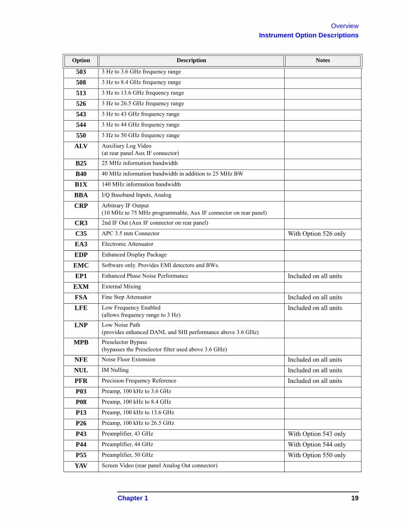
Instrument Option Descriptions
The PXA signal analyzer has a variety of hardware and measurement application options. Several of these options are “standard” so they are automatically installed on all PXA analyzers. All options require license files to be present in instrument memory before the option can be used, or viewed on the Show, System screen.
From the front panel, press System, Show, System to view a list of all installed options.
A current list of all instrument options and retrofit requirements is available on the Agilent web site for the PXA signal analyzer.
18 Chapter 1
Overview
Instrument Option Descriptions
Option Description Notes
503 3 Hz to 3.6 GHz frequency range
508 3 Hz to 8.4 GHz frequency range
513 3 Hz to 13.6 GHz frequency range
526 3 Hz to 26.5 GHz frequency range
543 3 Hz to 43 GHz frequency range
544 3 Hz to 44 GHz frequency range
550 3 Hz to 50 GHz frequency range
ALV Auxiliary Log Video (at rear panel Aux IF connector)
B25 25 MHz information bandwidth
B40 40 MHz information bandwidth in addition to 25 MHz BW
B1X 140 MHz information bandwidth
BBA I/Q Baseband Inputs, Analog
CRP Arbitrary IF Output (10 MHz to 75 MHz programmable, Aux IF connector on rear panel)
CR3 2nd IF Out (Aux IF connector on rear panel)
C35 APC 3.5 mm Connector With Option 526 only
EA3 Electronic Attenuator
EDP Enhanced Display Package
EMC Software only. Provides EMI detectors and BWs.
EP1 Enhanced Phase Noise Performance Included on all units
EXM External Mixing
FSA Fine Step Attenuator Included on all units
LFE Low Frequency Enabled(allows frequency range to 3 Hz)
Included on all units
LNP Low Noise Path(provides enhanced DANL and SHI performance above 3.6 GHz)
MPB Preselector Bypass(bypasses the Preselector filter used above 3.6 GHz)
NFE Noise Floor Extension Included on all units
NUL IM Nulling Included on all units
PFR Precision Frequency Reference Included on all units
P03 Preamp, 100 kHz to 3.6 GHz
P08 Preamp, 100 kHz to 8.4 GHz
P13 Preamp, 100 kHz to 13.6 GHz
P26 Preamp, 100 kHz to 26.5 GHz
P43 Preamplifier, 43 GHz With Option 543 only
P44 Preamplifier, 44 GHz With Option 544 only
P55 Preamplifier, 50 GHz With Option 550 only
YAV Screen Video (rear panel Analog Out connector)
Chapter 1 19
Overview
Signal Analyzer Accessories
Signal Analyzer Accessories
A number of accessories are available from Agilent Technologies to help you configure your analyzer for your specific applications. They can be ordered through your local Agilent Sales and Service Office and are listed below.
Manual Set on CD-ROM
The entire documentation set excluding the PXA Service Guide is shipped with the instrument on CD-ROM. The documentation that exists on the CD-ROM can also be accessed anytime via the web athttp://www.agilent.com/find/PXA_manuals.
Each manual is described below:
• Getting Started and Troubleshooting Guide: Describes analyzer features in detail. In addition, this manual covers unpacking and setting up the analyzer, analyzer features, and information on options and accessories, and what to do if you have a problem.
• Specifications Guide: Documents specifications, safety, and regulatory information.
• Instrument Messages: Includes instrument messages (and suggestions for troubleshooting them).
• Functional Tests: Includes manual functional tests.
• User’s/Programmer’s References: Multiple manuals which include programming information and SCPI command descriptions for basic spectrum analyzers and for applications such as IQ analyzer, WCDMA, and 802.16 OFDMA.
NOTE Refer to the front of the CD-ROM, for installation information.
NOTE Service documentation is not included in the standard documentation set. Refer to http://www.agilent.com/find/PXA_upgrades
20 Chapter 1
Overview
Signal Analyzer Accessories
50 Ohm Load
The Agilent 909 series loads come in several models and options providing a variety of frequency ranges and VSWRs. Also, they are available in either 50 ohm or 75 Ohm. Some examples include the:
909A: DC to 18 GHz909C: DC to 2 GHz909D: DC to 26.5 GHz
50 Ohm/75 Ohm Minimum Loss Pad
The Agilent 11852B is a low VSWR minimum loss pad that allows you to make measurements on 75 Ohm devices using an analyzer with a 50 Ohm input. It is effective over a frequency range of dc to 2 GHz.
75 Ohm Matching Transformer
The Agilent 11694A allows you to make measurements in 75 Ohm systems using an analyzer with a 50 Ohm input. It is effective over a frequency range of 3 to 500 MHz.
AC Probe
The Agilent 85024A high frequency probe performs in-circuit measurements without adversely loading the circuit under test. The probe has an input capacitance of 0.7 pF shunted by 1 MΩ of resistance and operates over a frequency range of 300 kHz to 3 GHz. High probe sensitivity and low distortion levels allow measurements to be made while taking advantage of the full dynamic range of the spectrum analyzer.
AC Probe (Low Frequency)
The Agilent 41800A low frequency probe has a low input capacitance and a frequency range of 5 Hz to 500 MHz.
Chapter 1 21
Overview
Signal Analyzer Accessories
Broadband Preamplifiers and Power Amplifiers
Preamplifiers and power amplifiers can be used with your spectrum analyzer to enhance measurements of very low-level signals.
• The Agilent 8447D preamplifier provides a minimum of 25 dB gain from 100 kHz to 1.3 GHz.
• The Agilent 87405B preamplifier provides a minimum of 22 dB gain from 10 MHz to 4 GHz. (Power is supplied by the probe power output of the analyzer.)
• The Agilent 83006A preamplifier provides a minimum of 26 dB gain from 10 MHz to 26.5 GHz.
• The 11909A low noise preamplifier provides a minimum of 32 dB gain from 9 kHz to 1 GHz and a typical noise figure of 1.8 dB.
RF and Transient Limiters
The Agilent 11867A and N9355C RF Limiters protect the analyzer input circuits from damage due to high power levels. The 11867A operates over a frequency range of dc to 1800 MHz and begins reflecting signal levels over 1 mW up to 10 W average power and 100 watts peak power. The N9355C microwave limiter (0.01 to 26.5 GHz) guards against input signals over 10 milliwatts up to 1 watt average power.
The Agilent 11947A Transient Limiter protects the analyzer input circuits from damage due to signal transients. It specifically is needed for use with a line impedance stabilization network (LISN). It operates over a frequency range of 9 kHz to 200 MHz, with 10 dB of insertion loss.
Power Splitters
The Agilent 11667A/B/C power splitters are two-resistor type splitters that provide excellent output SWR, at 50 Ω impedance. The tracking between the two output arms, over a broad frequency range, allows wideband measurements to be made with a minimum of uncertainty.
11667A: DC to 18 GHz11667B: DC to 26.5 GHz11667C: DC to 50 GHz
Static Safe Accessories
9300-1367 Wrist-strap, color black, stainless steel. Four adjustable links and a 7 mm post-type connection.
9300-0980 Wrist-strap cord 1.5 m (5 ft.)
9300-0797 2 ft by 4 ft conductive mat with 15 ft grounding wire
22 Chapter 1
Overview
Before You Start Troubleshooting
Before You Start Troubleshooting
Before troubleshooting, complete the following tasks:
❏ Familiarize yourself with the safety symbols marked on the instrument and read the general safety considerations in the front of this guide.
❏ Read the ESD information below.
❏ Familiarize yourself with the troubleshooting information in Chapter 2, “Boot Up and Initialization Troubleshooting”, and how it relates to information on troubleshooting the other assemblies.
WARNING These servicing instructions are for use by qualified personnel only. To avoid electrical shock, do not perform any servicing unless you are qualified to do so.
WARNING The opening of covers or removal of parts is likely to expose dangerous voltages. Disconnect the product from all voltage sources while it is being opened.
WARNING The detachable power cord is the instrument disconnecting device. It disconnects the mains circuits from the mains supply before other parts of the instrument. The front panel switch is only a standby switch and is not a LINE switch (disconnecting device).
CAUTION Always position the instrument for easy access to the disconnecting device (detachable power cord).
WARNING To prevent electrical shock, disconnect the analyzer from mains before cleaning. Use a dry cloth or one slightly dampened with water to clean the external case parts. Do not attempt to clean internally.
Chapter 1 23
Overview
Before You Start Troubleshooting
WARNING This is a Safety Class 1 Product (provided with a protective earthing ground incorporated in the power cord). The mains plug shall only be inserted in a socket outlet provided with a protective earth contact. Any interruption of the protective conductor inside or outside of the product is likely to make the product dangerous. Intentional interruption is prohibited.
CAUTION Always use the three-prong ac power cord supplied with this product. Failure to ensure adequate earth grounding by not using this cord may cause product damage.
CAUTION This instrument has an autoranging line voltage input; be sure the supply voltage is within the specified range.
24 Chapter 1
Overview
ESD Information
ESD Information
Protection from Electrostatic Discharge
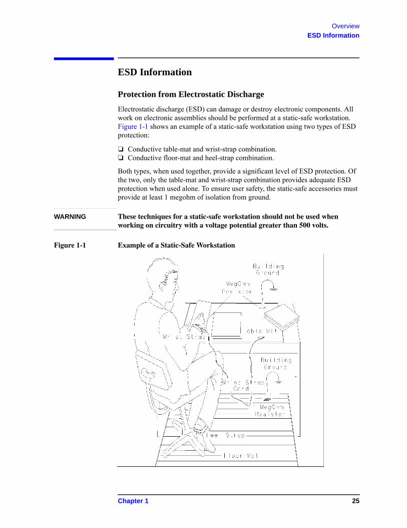
Electrostatic discharge (ESD) can damage or destroy electronic components. All work on electronic assemblies should be performed at a static-safe workstation. Figure 1-1 shows an example of a static-safe workstation using two types of ESD protection:
❏ Conductive table-mat and wrist-strap combination.❏ Conductive floor-mat and heel-strap combination.
Both types, when used together, provide a significant level of ESD protection. Of the two, only the table-mat and wrist-strap combination provides adequate ESD protection when used alone. To ensure user safety, the static-safe accessories must provide at least 1 megohm of isolation from ground.
WARNING These techniques for a static-safe workstation should not be used when working on circuitry with a voltage potential greater than 500 volts.
Figure 1-1 Example of a Static-Safe Workstation
Chapter 1 25
Overview
ESD Information
Handling of Electronic Components and ESD
The possibility of unseen damage caused by ESD is present whenever components are transported, stored, or used. The risk of ESD damage can be greatly reduced by paying close attention to how all components are handled.
❏ Perform work on all components at a static-safe workstation.
❏ Keep static-generating materials at least one meter away from all components.
❏ Store or transport components in static-shielding containers.
CAUTION Always handle printed circuit board assemblies by the edges. This will reduce the possibility of ESD damage to components and prevent contamination of exposed plating.
Test Equipment Usage and ESD
❏ Before connecting any coaxial cable to an analyzer connector, momentarily short the center and outer conductors of the cable together.
❏ Personnel should be grounded with a 1 megohm resistor-isolated wrist-strap before touching the center pin of any connector and before removing any assembly from the analyzer.
❏ Be sure that all analyzers are properly earth-grounded to prevent build-up of static charge.
For Additional Information about ESD
For more information about preventing ESD damage, contact the Electrical Over Stress/Electrostatic Discharge (EOS/ESD) Association, Inc. The ESD standards developed by this agency are sanctioned by the American National Standards Institute (ANSI).
26 Chapter 1
Overview
Service Equipment You Will Need
Service Equipment You Will Need
There are certain things that will be required to troubleshoot, adjust, and test the PXA Signal Analyzer. They include the following:
• Calibration Application Software• Front End Controller Troubleshooting Kit• USB Keyboard and Mouse• USB Storage Device• Test Equipment
Tools you will need
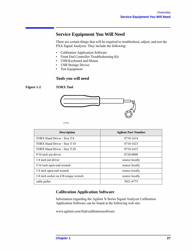
Figure 1-2 TORX Tool
Calibration Application Software
Information regarding the Agilent X-Series Signal Analyzer Calibration Application Software can be found at the following web site:
www.agilent.com/find/calibrationsoftware
Description Agilent Part Number
TORX Hand Driver - Size T-8 8710-1614
TORX Hand Driver - Size T-10 8710-1623
TORX Hand Driver - Size T-20 8710-1615
9/16 inch nut driver 8720-0008
1/4 inch nut driver source locally
5/16 inch open-end wrench source locally
1/4 inch open-end wrench source locally
1/4 inch socket on 4 lb torque wrench source locally
cable puller 5021-6773
Chapter 1 27
Overview
Service Equipment You Will Need
Front End Controller Troubleshooting Kit
The Front End Troubleshooting kit contains a PC board, required cables, and installation instructions to verify the switch control logic from the A15 Front End Control board to the lower level front end components is correct. Oftentimes when troubleshooting an RF front end problem, the logic needs to be verified before one of the front end components is changed. This troubleshooting kit will help identify the defective area in a timely manner. In order to effectively isolate A15 Front End Control board problems from front end component problems, it is highly recommended that the N9020-60005 Front End Troubleshooting kit is purchased.
The Front End Troubleshooting kit lower level items can be purchased individually or as a complete kit with instructions. The complete listing of kit components, descriptions, and part numbers can be found below.
Agilent Part Agilent Part Number Notes
Front End Troubleshooting kit N9020-60005
Front End Troubleshooting board E4410-60115 Part of N9020-60005 Troubleshooting kit
Cable, Low Band switch E4410-60160 Part of N9020-60005 Troubleshooting kit
Cable, RF Downconverter E4410-60156 Part of N9020-60005 Troubleshooting kit
Cable, YTF Preselector E4410-60158 Part of N9020-60005 Troubleshooting kit
Cable, Input Attenuators E4410-60157 Part of N9020-60005 Troubleshooting kit
Cable, Troubleshooting 8121-1400 Right-angle sma (m) to right-angle mmcx (m)(must be ordered separately)
Connector, MMCX (f) to SMA (f) n/a www.hubersuhner.comitem number: 31_MMCX-SMZ-50-1/111_OE(must be ordered separately)
28 Chapter 1
Overview
Service Equipment You Will Need
USB Keyboard and Mouse
A USB keyboard and mouse will be needed to accomplish many of the different troubleshooting tasks, as well as updating the instrument software. Any standard USB keyboard and mouse should work, but you can use the optional keyboard and mouse sold for the instrument. These can be purchased as:
USB Storage Device
The main reason why a USB storage device will be needed is to download instrument software and backup calibration data when the hard drive in an instrument needs to be replaced. The instrument software is about 1 GB. The calibration files are around 30 megabytes.
Description Option Number Upgrade Option Part Number
USB Keyboard N9030A-KYB N9030AK-KYB 0960-2961
USB Mouse N9030A-MSE N9030AK-MSE 0960-2670
Chapter 1 29
Overview
Service Equipment You Will Need
Required Test Equipment List
The following table identifies the equipment recommended for troubleshooting, adjusting, and verifying the performance of the instrument. Only the recommended and alternate equipment is compatible with the performance verification testing. Some tests can use various models of a particular equipment type. The “Recommended Agilent Model” is the preferred equipment. However, the “Alternative Agilent Model” is an acceptable substitute.
Table 1-1 Required Test Equipment
Instrument Critical Specifications Recommended Agilent
Model Numbera or Vendor Model Number
Alternative Agilent Model
Numbera
Useb
Signal Sources
Microwave Signal Generator #1 Frequency: 10 MHz to 50 GHzFrequency Resolution: 1 HzHarmonic level: < −30 dBcAmplitude range: −40 dBm to +13 dBmAmplitude resolution: 0.02VSWR: < 20 GHz: 1.6:1
≤ 31 GHz: 1.8:1
E8257D (Option 567, 1EA/1EU, 1E1) (Option 007, Analog Ramp Sweep, required for Frequency Response Adjustments)
For Adjustments:83630A/B/L(Option 001, 008),83640A/B/L(Option 001, 008), 83650A/B/L(Option 001, 008),
PSGc
For Performance Tests:83630A/B(Option 001, 008),83640A/B(Option 001, 008), 83650A/B(Option 001, 008)
PSGc
A, P, T
Microwave Signal Generator #2(only required for Third Order Intermodulation and Gain Compression)
Frequency: 10 MHz to 26.5 GHzFrequency Resolution: 1 HzHarmonic level: < −30 dBcAmplitude range: −20 dBm to +13Amplitude resolution: 0.02VSWR: < 20 GHz: 1.6:1
≤ 31 GHz: 1.8:1
E8257D(Option 1EA/1EU)
83630A/B(Option 008),83640A/B(Option 008), 83650A/B(Option 008)
PSGc
P
Low NoiseSignal Generator(one PSG may be used formultiple sources.
See footnote c)
Frequency: 50 MHz to 1.0 GHz Harmonics: < -30 dBc ≤ +13 dBmSpectral Purity SSB Phase Noise @ 1 GHz:
−112 dBc at 100 Hz offset−121 dBc at 1 kHz offset−131 dBc at 10 kHz offset
VSWR: < 1.5:1
E8257D(Options UNR, UNX, or UNY)
8663A
PSGc
(Options UNR, UNX, or UNY)
A, P, T
30 Chapter 1
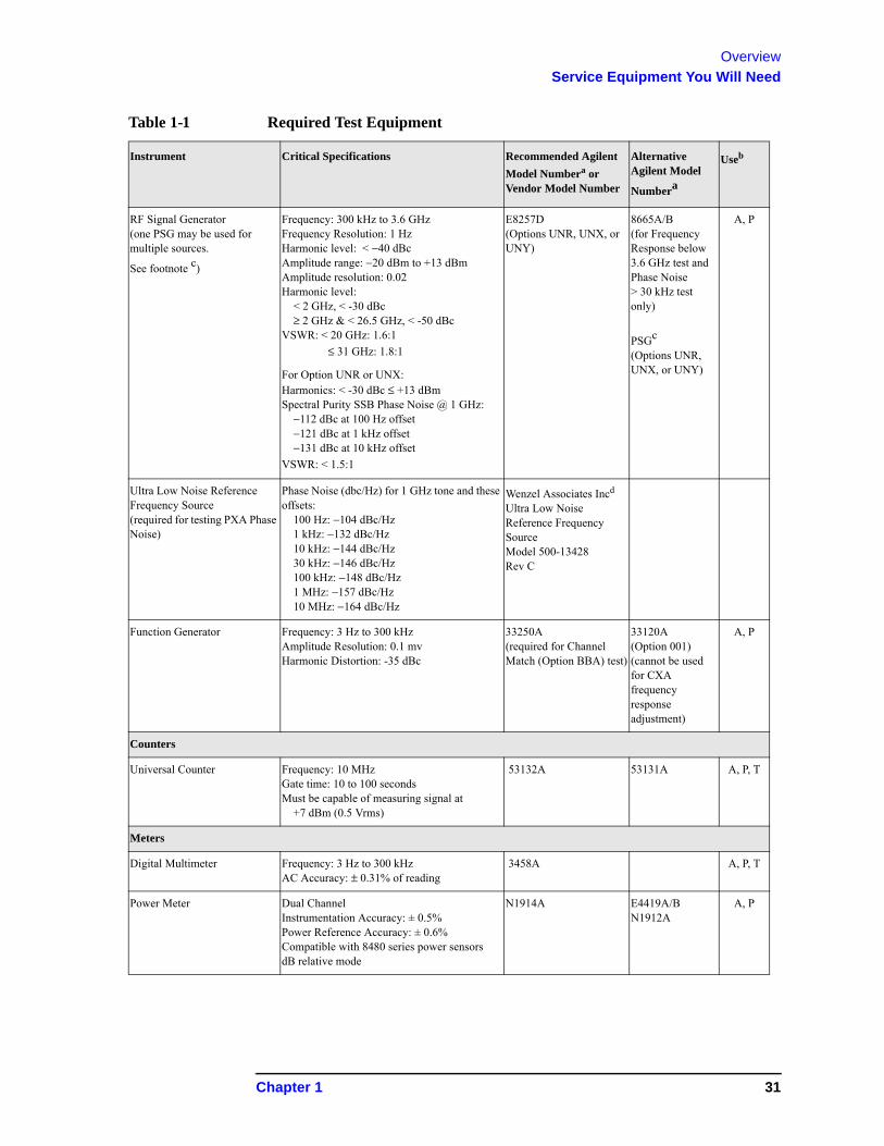
Overview
Service Equipment You Will Need
RF Signal Generator(one PSG may be used formultiple sources.
See footnote c)
Frequency: 300 kHz to 3.6 GHzFrequency Resolution: 1 HzHarmonic level: < −40 dBcAmplitude range: −20 dBm to +13 dBmAmplitude resolution: 0.02Harmonic level:
< 2 GHz, < -30 dBc ≥ 2 GHz & < 26.5 GHz, < -50 dBc
VSWR: < 20 GHz: 1.6:1
≤ 31 GHz: 1.8:1
For Option UNR or UNX:Harmonics: < -30 dBc ≤ +13 dBmSpectral Purity SSB Phase Noise @ 1 GHz:
−112 dBc at 100 Hz offset−121 dBc at 1 kHz offset−131 dBc at 10 kHz offset
VSWR: < 1.5:1
E8257D(Options UNR, UNX, or UNY)
8665A/B(for Frequency Response below 3.6 GHz test and Phase Noise > 30 kHz test only)
PSGc
(Options UNR, UNX, or UNY)
A, P
Ultra Low Noise Reference Frequency Source(required for testing PXA Phase Noise)
Phase Noise (dbc/Hz) for 1 GHz tone and these offsets:
100 Hz: −104 dBc/Hz1 kHz: −132 dBc/Hz10 kHz: −144 dBc/Hz30 kHz: −146 dBc/Hz100 kHz: −148 dBc/Hz1 MHz: −157 dBc/Hz10 MHz: −164 dBc/Hz
Wenzel Associates Incd
Ultra Low NoiseReference Frequency SourceModel 500-13428Rev C
Function Generator Frequency: 3 Hz to 300 kHzAmplitude Resolution: 0.1 mvHarmonic Distortion: -35 dBc
33250A(required for Channel Match (Option BBA) test)
33120A(Option 001)(cannot be used for CXA frequency response adjustment)
A, P
Counters
Universal Counter Frequency: 10 MHzGate time: 10 to 100 secondsMust be capable of measuring signal at
+7 dBm (0.5 Vrms)
53132A 53131A A, P, T
Meters
Digital Multimeter Frequency: 3 Hz to 300 kHzAC Accuracy: ± 0.31% of reading
3458A A, P, T
Power Meter Dual ChannelInstrumentation Accuracy: ± 0.5%Power Reference Accuracy: ± 0.6%Compatible with 8480 series power sensorsdB relative mode
N1914A E4419A/BN1912A
A, P
Table 1-1 Required Test Equipment
Instrument Critical Specifications Recommended Agilent
Model Numbera or Vendor Model Number
Alternative Agilent Model
Numbera
Useb
Chapter 1 31
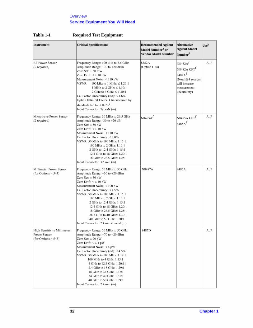
Overview
Service Equipment You Will Need
RF Power Sensor(2 required)
Frequency Range: 100 kHz to 3.6 GHzAmplitude Range: −30 to +20 dBmZero Set: ± 50 mWZero Drift: < ± 10 nWMeasurement Noise: < 110 nWVSWR 100 kHz to 1 MHz: ≤ 1.20:1
1 MHz to 2 GHz: ≤ 1.10:12 GHz to 3 GHz: ≤ 1.30:1
Cal Factor Uncertainty (std): < 1.6%Option H84 Cal Factor: Characterized by
standards lab to: ± 0.6%e
Input Connector: Type-N (m)
8482A(Option H84)
N8482Af
N8482A CFTf
8482Af
(Non H84 sensors will increase measurement uncertainty)
A, P
Microwave Power Sensor(2 required)
Frequency Range: 50 MHz to 26.5 GHzAmplitude Range: -30 to +20 dBZero Set: ± 50 nWZero Drift: < ± 10 nWMeasurement Noise: < 110 nWCal Factor Uncertainty: < 3.0%VSWR: 50 MHz to 100 MHz: 1.15:1
100 MHz to 2 GHz: 1.10:1 2 GHz to 12.4 GHz: 1.15:1 12.4 GHz to 18 GHz: 1.20:1 18 GHz to 26.5 GHz: 1.25:1
Input Connector: 3.5 mm (m)
N8485Af N8485A CFTf
8485Af
A, P
Millimeter Power Sensor(for Options > 543)
Frequency Range: 50 MHz to 50 GHzAmplitude Range: −30 to +20 dBmZero Set: ± 50 nWZero Drift: < ± 10 nWMeasurement Noise: < 100 nWCal Factor Uncertainty: < 4.5%VSWR: 50 MHz to 100 MHz: 1.15:1
100 MHz to 2 GHz: 1.10:1 2 GHz to 12.4 GHz: 1.15:1 12.4 GHz to 18 GHz: 1.20:1 18 GHz to 26.5 GHz: 1.25:126.5 GHz to 40 GHz: 1.30:140 GHz to 50 GHz: 1.50:1
Input Connector: 2.4 mm coaxial (m)
N8487A 8487A A, P
High Sensitivity Millimeter Power Sensor(for Options > 543)
Frequency Range: 50 MHz to 50 GHzAmplitude Range: −70 to −20 dBmZero Set: ± 20 pWZero Drift: < ± 4 pWMeasurement Noise: < 4 pWCal Factor Uncertainty (std): < 4.5%VSWR: 50 MHz to 100 MHz: 1.19:1
100 MHz to 4 GHz: 1.15:14 GHz to 12.4 GHz: 1.20:112.4 GHz to 18 GHz: 1.29:118 GHz to 34 GHz: 1.37:134 GHz to 40 GHz: 1.61:140 GHz to 50 GHz: 1.89:1
Input Connector: 2.4 mm (m)
8487D A, P
Table 1-1 Required Test Equipment
Instrument Critical Specifications Recommended Agilent
Model Numbera or Vendor Model Number
Alternative Agilent Model
Numbera
Useb
32 Chapter 1
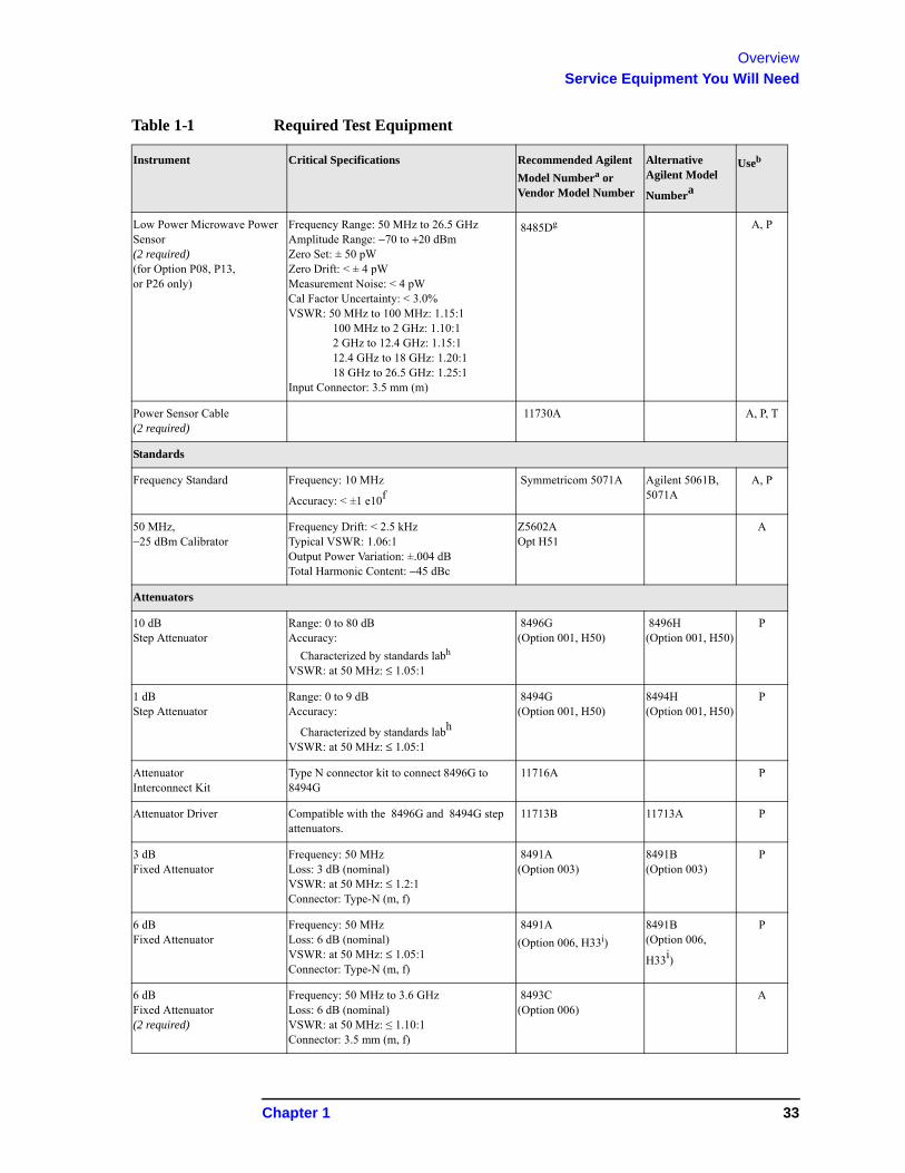
Overview
Service Equipment You Will Need
Low Power Microwave Power Sensor(2 required)(for Option P08, P13, or P26 only)
Frequency Range: 50 MHz to 26.5 GHzAmplitude Range: −70 to +20 dBmZero Set: ± 50 pWZero Drift: < ± 4 pWMeasurement Noise: < 4 pWCal Factor Uncertainty: < 3.0%VSWR: 50 MHz to 100 MHz: 1.15:1
100 MHz to 2 GHz: 1.10:1 2 GHz to 12.4 GHz: 1.15:1 12.4 GHz to 18 GHz: 1.20:1 18 GHz to 26.5 GHz: 1.25:1
Input Connector: 3.5 mm (m)
8485Dg A, P
Power Sensor Cable(2 required)
11730A A, P, T
Standards
Frequency Standard Frequency: 10 MHz
Accuracy: < ±1 e10fSymmetricom 5071A Agilent 5061B,
5071AA, P
50 MHz,−25 dBm Calibrator
Frequency Drift: < 2.5 kHzTypical VSWR: 1.06:1Output Power Variation: ±.004 dBTotal Harmonic Content: −45 dBc
Z5602A Opt H51
A
Attenuators
10 dB Step Attenuator
Range: 0 to 80 dBAccuracy:
Characterized by standards labh
VSWR: at 50 MHz: ≤ 1.05:1
8496G(Option 001, H50)
8496H(Option 001, H50)
P
1 dB Step Attenuator
Range: 0 to 9 dBAccuracy:
Characterized by standards labh
VSWR: at 50 MHz: ≤ 1.05:1
8494G(Option 001, H50)
8494H(Option 001, H50)
P
Attenuator Interconnect Kit
Type N connector kit to connect 8496G to 8494G
11716A P
Attenuator Driver Compatible with the 8496G and 8494G step attenuators.
11713B 11713A P
3 dB Fixed Attenuator
Frequency: 50 MHzLoss: 3 dB (nominal)VSWR: at 50 MHz: ≤ 1.2:1Connector: Type-N (m, f)
8491A(Option 003)
8491B(Option 003)
P
6 dB Fixed Attenuator
Frequency: 50 MHzLoss: 6 dB (nominal)VSWR: at 50 MHz: ≤ 1.05:1Connector: Type-N (m, f)
8491A
(Option 006, H33i)
8491B(Option 006,
H33i)
P
6 dB Fixed Attenuator(2 required)
Frequency: 50 MHz to 3.6 GHzLoss: 6 dB (nominal)VSWR: at 50 MHz: ≤ 1.10:1Connector: 3.5 mm (m, f)
8493C(Option 006)
A
Table 1-1 Required Test Equipment
Instrument Critical Specifications Recommended Agilent
Model Numbera or Vendor Model Number
Alternative Agilent Model
Numbera
Useb
Chapter 1 33
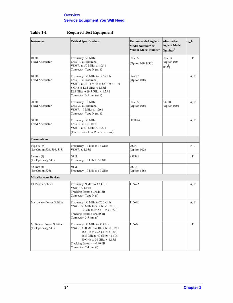
Overview
Service Equipment You Will Need
10 dB Fixed Attenuator
Frequency: 50 MHzLoss: 10 dB (nominal)VSWR: at 50 MHz: ≤ 1.05:1Connector: Type-N (m, f)
8491A
(Option 010, H33i)
8491B(Option 010,
H33i)
P
10 dB Fixed Attenuator
Frequency: 50 MHz to 19.5 GHzLoss: 10 dB (nominal)VSWR: at 321.4 MHz to 8 GHz: ≤ 1.1:18 GHz to 12.4 GHz: < 1.15:112.4 GHz to 19.5 GHz: < 1.25:1Connector: 3.5 mm (m, f)
8493C(Option 010)
A, P
20 dB Fixed Attenuator
Frequency: 10 MHzLoss: 20 dB (nominal)VSWR: 10 MHz: ≤ 1.20:1Connector: Type-N (m, f)
8491A(Option 020)
8491B(Option 020)
A, P
30 dB Fixed Attenuator
Frequency: 50 MHzLoss: 30 dB ±.0.05 dBVSWR: at 50 MHz: ≤ 1.05:1
(For use with Low Power Sensors)
11708A A, P
Terminations
Type-N (m)(for Option 503, 508, 513)
Frequency: 10 kHz to 18 GHzVSWR: ≤ 1.05:1
909A (Option 012)
P, T
2.4 mm (f)(for Options > 543)
50 ΩFrequency: 10 kHz to 50 GHz
85138B P
3.5 mm (f)(for Option 526)
50 ΩFrequency: 10 kHz to 50 GHz
909D(Option 526)
Miscellaneous Devices
RF Power Splitter Frequency: 9 kHz to 3.6 GHzVSWR: ≤ 1.10:1Tracking Error: < ± 0.15 dBConnector: Type-N (f)
11667A A, P
Microwave Power Splitter Frequency: 50 MHz to 26.5 GHzVSWR: 50 MHz to 3 GHz: < 1.22:1
3 GHz to 26.5 GHz: < 1.22:1Tracking Error: < ± 0.40 dBConnector: 3.5 mm (f)
11667B A, P
Millimeter Power Splitter (for Options > 543)
Frequency: 50 MHz to 50 GHzVSWR: ≤ 50 MHz to 18 GHz: < 1.29:1
18 GHz to 26.5 GHz: <1.20:126.5 GHz to 40 GHz: < 1.50:140 GHz to 50 GHz: < 1.65:1
Tracking Error: < ± 0.40 dBConnector: 2.4 mm (f)
11667C P
Table 1-1 Required Test Equipment
Instrument Critical Specifications Recommended Agilent
Model Numbera or Vendor Model Number
Alternative Agilent Model
Numbera
Useb
34 Chapter 1
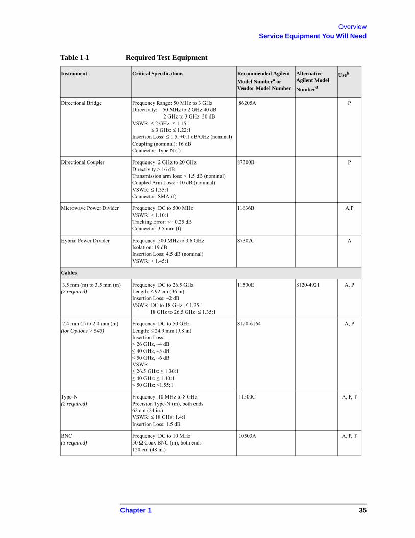
Overview
Service Equipment You Will Need
Directional Bridge Frequency Range: 50 MHz to 3 GHzDirectivity: 50 MHz to 2 GHz:40 dB
2 GHz to 3 GHz: 30 dBVSWR: ≤ 2 GHz: ≤ 1.15:1
≤ 3 GHz: ≤ 1.22:1Insertion Loss: ≤ 1.5, +0.1 dB/GHz (nominal)Coupling (nominal): 16 dBConnector: Type N (f)
86205A P
Directional Coupler Frequency: 2 GHz to 20 GHzDirectivity > 16 dBTransmission arm loss: < 1.5 dB (nominal)Coupled Arm Loss: ~10 dB (nominal) VSWR: ≤ 1.35:1Connector: SMA (f)
87300B P
Microwave Power Divider Frequency: DC to 500 MHzVSWR: < 1.10:1Tracking Error: <± 0.25 dBConnector: 3.5 mm (f)
11636B A,P
Hybrid Power Divider Frequency: 500 MHz to 3.6 GHzIsolation: 19 dBInsertion Loss: 4.5 dB (nominal)VSWR: < 1.45:1
87302C A
Cables
3.5 mm (m) to 3.5 mm (m)(2 required)
Frequency: DC to 26.5 GHzLength: ≤ 92 cm (36 in) Insertion Loss: ~2 dBVSWR: DC to 18 GHz: ≤ 1.25:1
18 GHz to 26.5 GHz: ≤ 1.35:1
11500E 8120-4921 A, P
2.4 mm (f) to 2.4 mm (m)(for Options > 543)
Frequency: DC to 50 GHzLength: ≤ 24.9 mm (9.8 in)Insertion Loss:≤ 26 GHz, ~4 dB≤ 40 GHz, ~5 dB≤ 50 GHz, ~6 dBVSWR:≤ 26.5 GHz: ≤ 1.30:1≤ 40 GHz: ≤ 1.40:1≤ 50 GHz: ≤1.55:1
8120-6164 A, P
Type-N(2 required)
Frequency: 10 MHz to 8 GHzPrecision Type-N (m), both ends62 cm (24 in.) VSWR: ≤ 18 GHz: 1.4:1 Insertion Loss: 1.5 dB
11500C A, P, T
BNC(3 required)
Frequency: DC to 10 MHz50 Ω Coax BNC (m), both ends120 cm (48 in.)
10503A A, P, T
Table 1-1 Required Test Equipment
Instrument Critical Specifications Recommended Agilent
Model Numbera or Vendor Model Number
Alternative Agilent Model
Numbera
Useb
Chapter 1 35
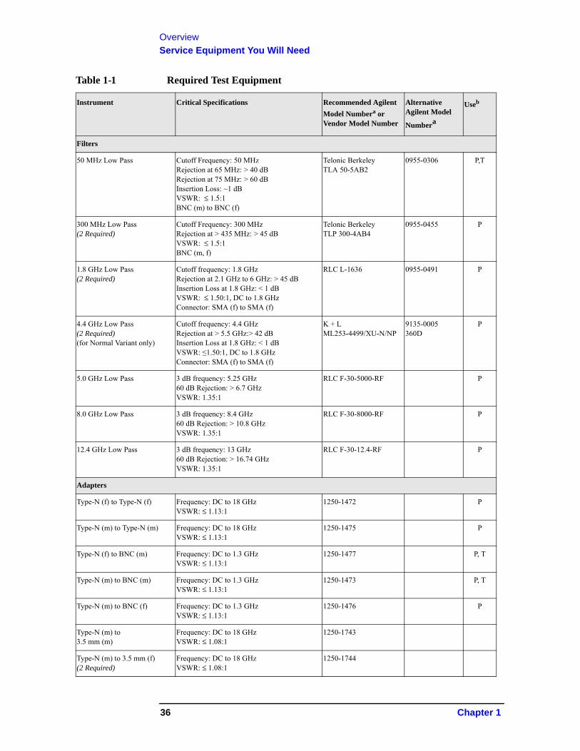
Overview
Service Equipment You Will Need
Filters
50 MHz Low Pass Cutoff Frequency: 50 MHzRejection at 65 MHz: > 40 dBRejection at 75 MHz: > 60 dBInsertion Loss: ~1 dBVSWR: ≤ 1.5:1 BNC (m) to BNC (f)
Telonic BerkeleyTLA 50-5AB2
0955-0306 P,T
300 MHz Low Pass(2 Required)
Cutoff Frequency: 300 MHzRejection at > 435 MHz: > 45 dBVSWR: ≤ 1.5:1BNC (m, f)
Telonic BerkeleyTLP 300-4AB4
0955-0455 P
1.8 GHz Low Pass(2 Required)
Cutoff frequency: 1.8 GHzRejection at 2.1 GHz to 6 GHz: > 45 dBInsertion Loss at 1.8 GHz: < 1 dBVSWR: ≤ 1.50:1, DC to 1.8 GHzConnector: SMA (f) to SMA (f)
RLC L-1636 0955-0491 P
4.4 GHz Low Pass(2 Required)(for Normal Variant only)
Cutoff frequency: 4.4 GHzRejection at > 5.5 GHz:> 42 dBInsertion Loss at 1.8 GHz: < 1 dBVSWR: ≤1.50:1, DC to 1.8 GHzConnector: SMA (f) to SMA (f)
K + L ML253-4499/XU-N/NP
9135-0005360D
P
5.0 GHz Low Pass 3 dB frequency: 5.25 GHz60 dB Rejection: > 6.7 GHzVSWR: 1.35:1
RLC F-30-5000-RF P
8.0 GHz Low Pass 3 dB frequency: 8.4 GHz60 dB Rejection: > 10.8 GHzVSWR: 1.35:1
RLC F-30-8000-RF P
12.4 GHz Low Pass 3 dB frequency: 13 GHz60 dB Rejection: > 16.74 GHzVSWR: 1.35:1
RLC F-30-12.4-RF P
Adapters
Type-N (f) to Type-N (f) Frequency: DC to 18 GHzVSWR: ≤ 1.13:1
1250-1472 P
Type-N (m) to Type-N (m) Frequency: DC to 18 GHzVSWR: ≤ 1.13:1
1250-1475 P
Type-N (f) to BNC (m) Frequency: DC to 1.3 GHzVSWR: ≤ 1.13:1
1250-1477 P, T
Type-N (m) to BNC (m) Frequency: DC to 1.3 GHzVSWR: ≤ 1.13:1
1250-1473 P, T
Type-N (m) to BNC (f) Frequency: DC to 1.3 GHzVSWR: ≤ 1.13:1
1250-1476 P
Type-N (m) to 3.5 mm (m)
Frequency: DC to 18 GHzVSWR: ≤ 1.08:1
1250-1743
Type-N (m) to 3.5 mm (f)(2 Required)
Frequency: DC to 18 GHzVSWR: ≤ 1.08:1
1250-1744
Table 1-1 Required Test Equipment
Instrument Critical Specifications Recommended Agilent
Model Numbera or Vendor Model Number
Alternative Agilent Model
Numbera
Useb
36 Chapter 1
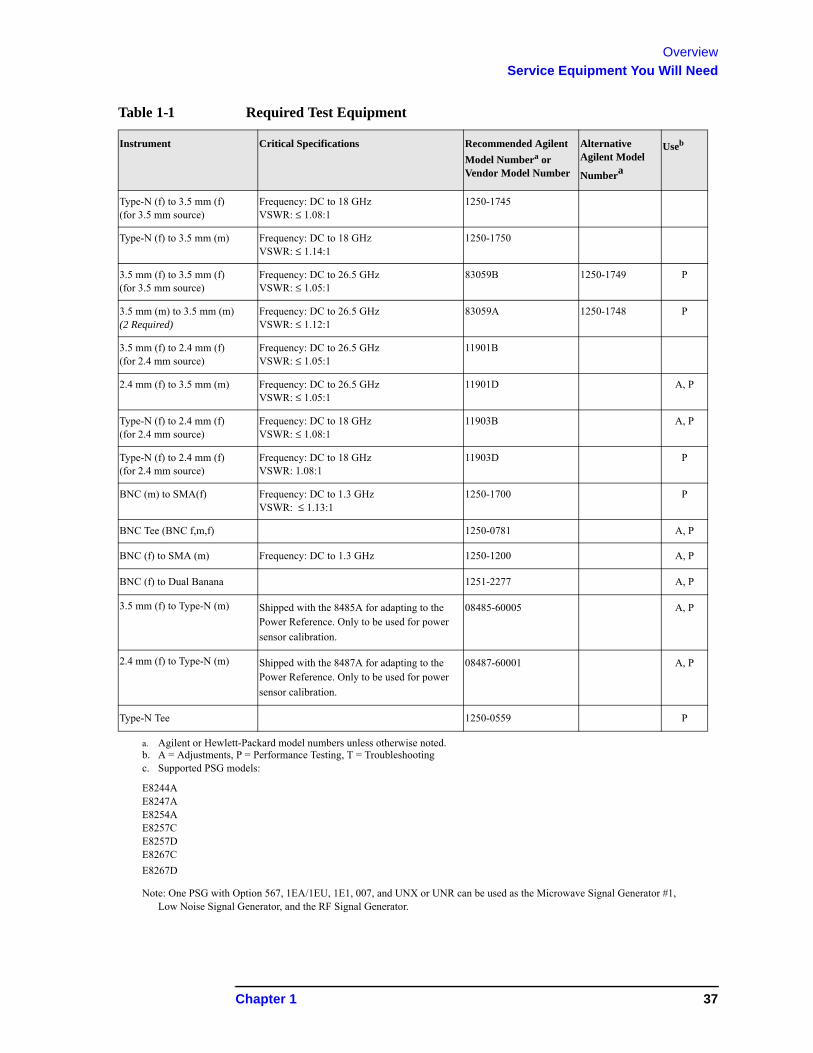
Overview
Service Equipment You Will Need
Type-N (f) to 3.5 mm (f)(for 3.5 mm source)
Frequency: DC to 18 GHzVSWR: ≤ 1.08:1
1250-1745
Type-N (f) to 3.5 mm (m) Frequency: DC to 18 GHzVSWR: ≤ 1.14:1
1250-1750
3.5 mm (f) to 3.5 mm (f)(for 3.5 mm source)
Frequency: DC to 26.5 GHzVSWR: ≤ 1.05:1
83059B 1250-1749 P
3.5 mm (m) to 3.5 mm (m)(2 Required)
Frequency: DC to 26.5 GHzVSWR: ≤ 1.12:1
83059A 1250-1748 P
3.5 mm (f) to 2.4 mm (f)(for 2.4 mm source)
Frequency: DC to 26.5 GHzVSWR: ≤ 1.05:1
11901B
2.4 mm (f) to 3.5 mm (m) Frequency: DC to 26.5 GHzVSWR: ≤ 1.05:1
11901D A, P
Type-N (f) to 2.4 mm (f)(for 2.4 mm source)
Frequency: DC to 18 GHzVSWR: ≤ 1.08:1
11903B A, P
Type-N (f) to 2.4 mm (f)(for 2.4 mm source)
Frequency: DC to 18 GHzVSWR: 1.08:1
11903D P
BNC (m) to SMA(f) Frequency: DC to 1.3 GHzVSWR: ≤ 1.13:1
1250-1700 P
BNC Tee (BNC f,m,f) 1250-0781 A, P
BNC (f) to SMA (m) Frequency: DC to 1.3 GHz 1250-1200 A, P
BNC (f) to Dual Banana 1251-2277 A, P
3.5 mm (f) to Type-N (m) Shipped with the 8485A for adapting to the Power Reference. Only to be used for power
sensor calibration.
08485-60005 A, P
2.4 mm (f) to Type-N (m) Shipped with the 8487A for adapting to the Power Reference. Only to be used for power
sensor calibration.
08487-60001 A, P
Type-N Tee 1250-0559 P
a. Agilent or Hewlett-Packard model numbers unless otherwise noted.b. A = Adjustments, P = Performance Testing, T = Troubleshootingc. Supported PSG models:
E8244AE8247AE8254AE8257CE8257DE8267C
E8267D
Note: One PSG with Option 567, 1EA/1EU, 1E1, 007, and UNX or UNR can be used as the Microwave Signal Generator #1, Low Noise Signal Generator, and the RF Signal Generator.
Table 1-1 Required Test Equipment
Instrument Critical Specifications Recommended Agilent
Model Numbera or Vendor Model Number
Alternative Agilent Model
Numbera
Useb
Chapter 1 37
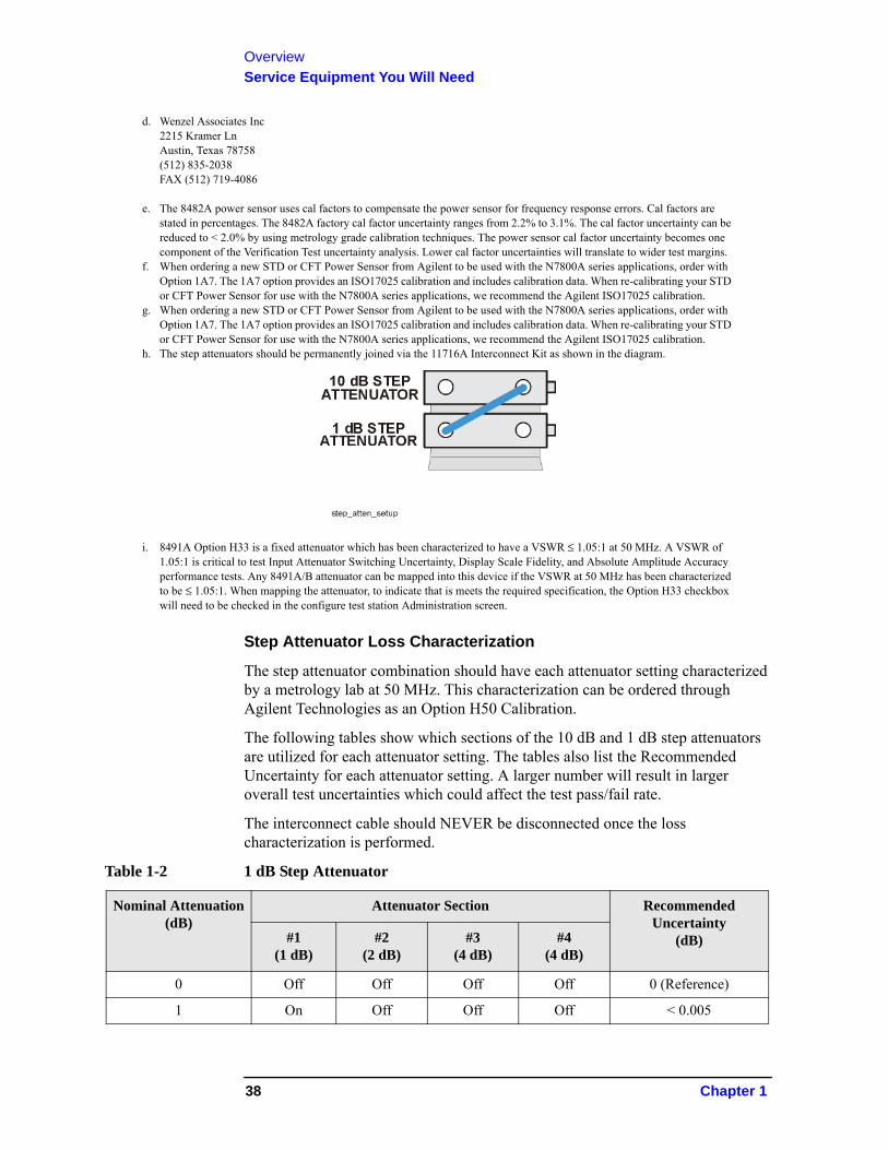
Overview
Service Equipment You Will Need
Step Attenuator Loss Characterization
The step attenuator combination should have each attenuator setting characterized by a metrology lab at 50 MHz. This characterization can be ordered through Agilent Technologies as an Option H50 Calibration.
The following tables show which sections of the 10 dB and 1 dB step attenuators are utilized for each attenuator setting. The tables also list the Recommended Uncertainty for each attenuator setting. A larger number will result in larger overall test uncertainties which could affect the test pass/fail rate.
The interconnect cable should NEVER be disconnected once the loss characterization is performed.
d. Wenzel Associates Inc2215 Kramer LnAustin, Texas 78758(512) 835-2038FAX (512) 719-4086
e. The 8482A power sensor uses cal factors to compensate the power sensor for frequency response errors. Cal factors are stated in percentages. The 8482A factory cal factor uncertainty ranges from 2.2% to 3.1%. The cal factor uncertainty can be reduced to < 2.0% by using metrology grade calibration techniques. The power sensor cal factor uncertainty becomes one component of the Verification Test uncertainty analysis. Lower cal factor uncertainties will translate to wider test margins.
f. When ordering a new STD or CFT Power Sensor from Agilent to be used with the N7800A series applications, order with Option 1A7. The 1A7 option provides an ISO17025 calibration and includes calibration data. When re-calibrating your STD or CFT Power Sensor for use with the N7800A series applications, we recommend the Agilent ISO17025 calibration.
g. When ordering a new STD or CFT Power Sensor from Agilent to be used with the N7800A series applications, order with Option 1A7. The 1A7 option provides an ISO17025 calibration and includes calibration data. When re-calibrating your STD or CFT Power Sensor for use with the N7800A series applications, we recommend the Agilent ISO17025 calibration.
h. The step attenuators should be permanently joined via the 11716A Interconnect Kit as shown in the diagram.
i. 8491A Option H33 is a fixed attenuator which has been characterized to have a VSWR ≤ 1.05:1 at 50 MHz. A VSWR of 1.05:1 is critical to test Input Attenuator Switching Uncertainty, Display Scale Fidelity, and Absolute Amplitude Accuracy performance tests. Any 8491A/B attenuator can be mapped into this device if the VSWR at 50 MHz has been characterized to be ≤ 1.05:1. When mapping the attenuator, to indicate that is meets the required specification, the Option H33 checkbox will need to be checked in the configure test station Administration screen.
Table 1-2 1 dB Step Attenuator
Nominal Attenuation (dB)
Attenuator Section Recommended Uncertainty
(dB)#1 (1 dB)
#2 (2 dB)
#3 (4 dB)
#4 (4 dB)
0 Off Off Off Off 0 (Reference)
1 On Off Off Off < 0.005
38 Chapter 1
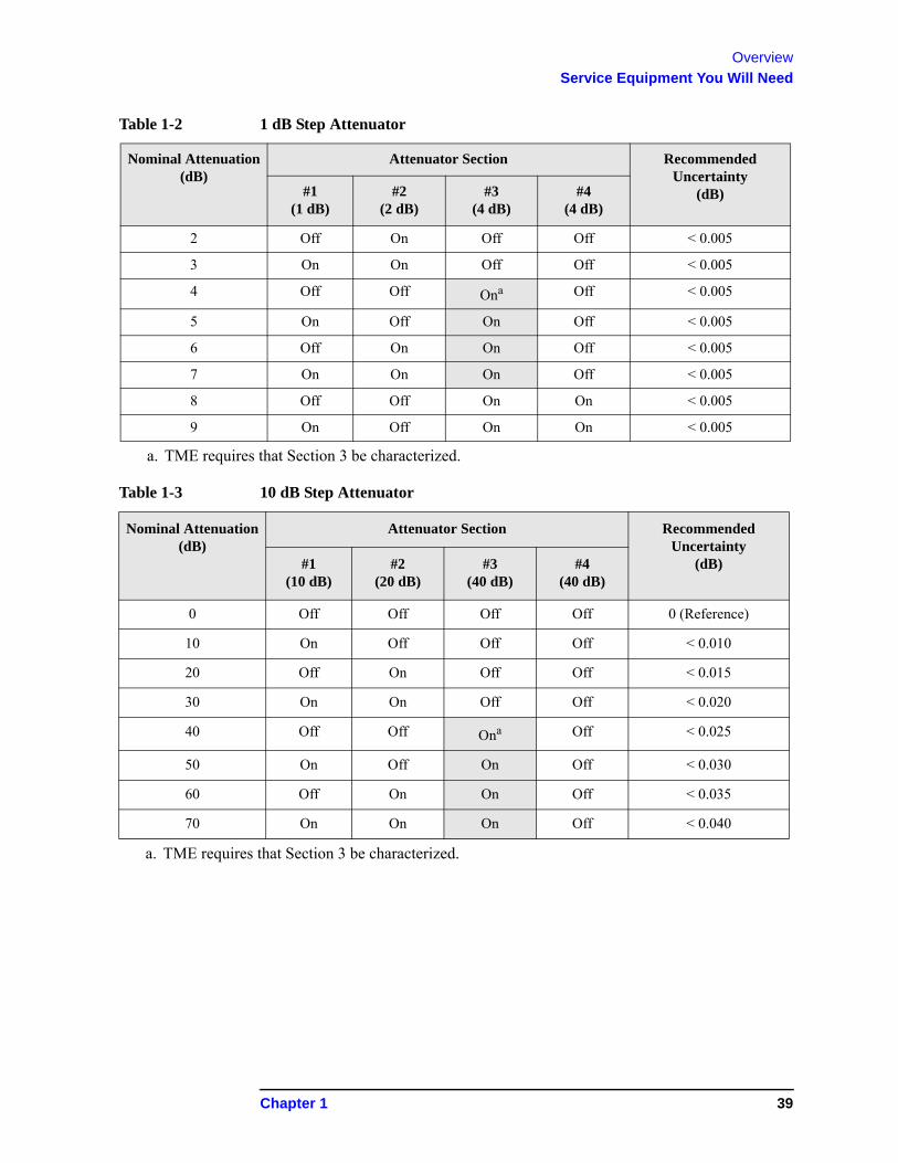
Overview
Service Equipment You Will Need
2 Off On Off Off < 0.005
3 On On Off Off < 0.005
4 Off Off Ona Off < 0.005
5 On Off On Off < 0.005
6 Off On On Off < 0.005
7 On On On Off < 0.005
8 Off Off On On < 0.005
9 On Off On On < 0.005
a. TME requires that Section 3 be characterized.
Table 1-3 10 dB Step Attenuator
Nominal Attenuation (dB)
Attenuator Section Recommended Uncertainty
(dB)#1 (10 dB)
#2 (20 dB)
#3 (40 dB)
#4 (40 dB)
0 Off Off Off Off 0 (Reference)
10 On Off Off Off < 0.010
20 Off On Off Off < 0.015
30 On On Off Off < 0.020
40 Off Off Ona Off < 0.025
50 On Off On Off < 0.030
60 Off On On Off < 0.035
70 On On On Off < 0.040
a. TME requires that Section 3 be characterized.
Table 1-2 1 dB Step Attenuator
Nominal Attenuation (dB)
Attenuator Section Recommended Uncertainty
(dB)#1 (1 dB)
#2 (2 dB)
#3 (4 dB)
#4 (4 dB)
Chapter 1 39
Overview
After an Instrument Repair
After an Instrument Repair
If any instrument assemblies have been repaired or replaced, perform the related adjustments and performance verification tests. These tests are done using the N7814A Agilent X-Series Signal Analyzer Calibration Application Software. Refer to Chapter 17 , “Post-Repair Procedures” for a list of post-repair adjustments and performance tests based on which hardware has been changed.
Information regarding the N7814A Agilent X-Series Signal Analyzer Calibration Application Software can be found at
http://www.agilent.com/find/calibrationsoftware
40 Chapter 1
Overview
Contacting Agilent Technologies
Contacting Agilent Technologies
If you have a problem with your instrument, see Chapter 2, “Boot Up and Initialization Troubleshooting”. This section contains a checklist that will help identify some of the most common problems.
There is also support on the world-wide web. The address is:
http://www.agilent.com/find/pxa_support
FAQs, instrument software updates, documentation, and other support information can be accessed from this site.
To obtain servicing information or to order replacement parts, contact the nearest Agilent office listed in Table 1-4. In any correspondence or telephone conversations, refer to the instrument by its model number (N9030A) and full serial number (ex. MY49250887). With this information, the Agilent representative can quickly determine whether your unit is still within its warranty period.
By internet, phone, or fax, get assistance with all your test and measurement needs.
Chapter 1 41
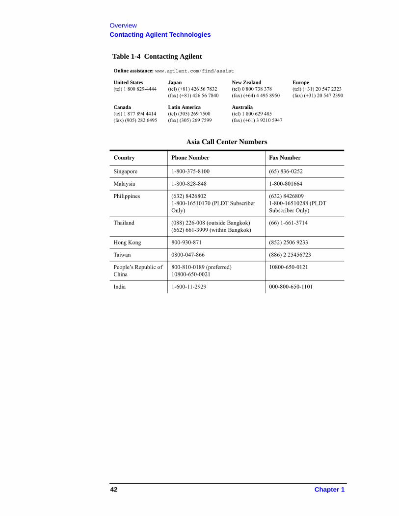
Overview
Contacting Agilent Technologies
Table 1-4 Contacting Agilent
Online assistance: www.agilent.com/find/assist
United States(tel) 1 800 829-4444
Japan(tel) (+81) 426 56 7832(fax) (+81) 426 56 7840
New Zealand(tel) 0 800 738 378(fax) (+64) 4 495 8950
Europe(tel) (+31) 20 547 2323(fax) (+31) 20 547 2390
Canada(tel) 1 877 894 4414(fax) (905) 282 6495
Latin America(tel) (305) 269 7500(fax) (305) 269 7599
Australia(tel) 1 800 629 485(fax) (+61) 3 9210 5947
Asia Call Center Numbers
Country Phone Number Fax Number
Singapore 1-800-375-8100 (65) 836-0252
Malaysia 1-800-828-848 1-800-801664
Philippines (632) 84268021-800-16510170 (PLDT Subscriber Only)
(632) 84268091-800-16510288 (PLDT Subscriber Only)
Thailand (088) 226-008 (outside Bangkok)(662) 661-3999 (within Bangkok)
(66) 1-661-3714
Hong Kong 800-930-871 (852) 2506 9233
Taiwan 0800-047-866 (886) 2 25456723
People’s Republic of China
800-810-0189 (preferred)10800-650-0021
10800-650-0121
India 1-600-11-2929 000-800-650-1101
42 Chapter 1
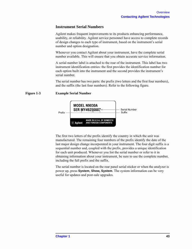
Overview
Contacting Agilent Technologies
Instrument Serial Numbers
Agilent makes frequent improvements to its products enhancing performance, usability, or reliability. Agilent service personnel have access to complete records of design changes to each type of instrument, based on the instrument’s serial number and option designation.
Whenever you contact Agilent about your instrument, have the complete serial number available. This will ensure that you obtain accurate service information.
A serial number label is attached to the rear of the instrument. This label has two instrument identification entries: the first provides the identification number for each option built into the instrument and the second provides the instrument’s serial number.
The serial number has two parts: the prefix (two letters and the first four numbers), and the suffix (the last four numbers). Refer to the following figure.
Figure 1-3 Example Serial Number
The first two letters of the prefix identify the country in which the unit was manufactured. The remaining four numbers of the prefix identify the date of the last major design change incorporated in your instrument. The four digit suffix is a sequential number and, coupled with the prefix, provides a unique identification for each unit produced. Whenever you list the serial number or refer to it in obtaining information about your instrument, be sure to use the complete number, including the full prefix and the suffix.
The serial number is located on the rear panel serial sticker or when the analyzer is power up, press System, Show, System. The system information can be very useful for updates and post-sale upgrades.
Chapter 1 43
Overview
How to Return Your Instrument for Service
How to Return Your Instrument for Service
Service Order Number
If an instrument is being returned to Agilent for servicing, the phone numbers are mentioned in Table 1-4, “Contacting Agilent,” on page 42. In order for Agilent to expedite the repair please be as specific as possible about the nature of the failure.
Helpful failure descriptions:
• Signal level measures 10 dB too low at 1 GHz
• LO Unlock error message appears on screen in spans < 10 MHz
• Analyzer will not complete boot up sequence to signal analyzer mode
Failure descriptions that will most likely increase repair time:
• Analyzer broken
• Analyzer will not make accurate measurements
• Signal drifts
If you have recorded any error messages that appeared on the analyzer display, or have completed a Functional Test or Performance Verification Test, or have any other specific data on the performance of the instrument, please send a copy of this information with the instrument.
Original Packaging
Before shipping, pack the unit in the original factory packaging materials if they are available. If the original materials were not retained, see “Other Packaging” on page 45.
44 Chapter 1
Overview
How to Return Your Instrument for Service
Other Packaging
CAUTION Instrument damage can result from using packaging materials other than those specified. Never use styrene pellets in any shape as packaging materials. They do not adequately cushion the equipment or prevent it from shifting in the carton. They cause equipment damage by generating static electricity and by lodging in the instrument louvers, blocking airflow.
You can repackage the instrument with commercially available materials, as follows:
1. Protect the control panel with cardboard.
2. Wrap the instrument in antistatic plastic to reduce the possibility of damage caused by electrostatic discharge.
3. Use a strong shipping container. A double-walled, corrugated cardboard carton with 159 kg (350 lb) bursting strength is adequate. The carton must be both large enough and strong enough to accommodate the instrument. Allow at least 3 to 4 inches on all sides of the instrument for packing material.
4. Surround the equipment with three to four inches of packing material and prevent the equipment from moving in the carton. If packing foam is not available, the best alternative is S.D.-240 Air Cap™ from Sealed Air Corporation, Hayward, California, 94545.
Air Cap looks like a plastic sheet filled with 1-1/4 inch air bubbles. Use the pink-colored Air Cap to reduce static electricity. Wrapping the equipment several times in this material should both protect the equipment and prevent it from moving in the carton.
5. Seal the shipping container securely with strong nylon adhesive tape.
6. Mark the shipping container “FRAGILE, HANDLE WITH CARE” to assure careful handling.
7. Retain copies of all shipping papers.
Chapter 1 45

Overview
How to Return Your Instrument for Service
46 Chapter 1

2 Boot Up and Initialization Troubleshooting
47
Boot Up and Initialization Troubleshooting
What You Will Find in This Chapter
What You Will Find in This Chapter
This chapter provides information that is useful when starting to troubleshoot a spectrum analyzer. It includes procedures for troubleshooting common failures and provides information on isolating problems in the analyzer.
The following sections are found in this chapter:
Check the Basics on page 49
PXA Instrument Boot Up Process on page 50
Typical instrument boot-up process flow on page 51
Potential Problems During Boot Process on page 54
Yellow Standby LED Does Not Illuminate on page 54
Green Power On LED Does Not Illuminate on page 56
Fan(s) Are Not Operating on page 60
No Agilent Splash Screen Displayed on page 62
Instrument Hangs at the Agilent Splash Screen on page 64
Instrument Cannot Completely Load or Run the Operating System on page 65
Troubleshooting a Blank Display on page 65
Initializations Did Not Complete on page 69
Fails an Initial Alignment on page 70
Signal Level Problem with Input Frequencies < 3.6 GHz on page 76
Signal Level Problem with Input Frequencies > 3.6 GHz on page 77
48 Chapter 2
Boot Up and Initialization Troubleshooting
Check the Basics
Check the Basics
Before calling Agilent Technologies or returning the instrument for service, please make the following checks:
1. Is there power at the power outlet? At the power receptacle on the instrument?
2. Is the instrument turned on? Check to see if the front panel LED is green, which indicates the power supply is on.
3. If other equipment, cables, and connectors are being used with the instrument, make sure they are connected properly.
4. Review the procedure for the measurement being performed when the problem appeared. Are all the settings correct?
5. If the instrument is not functioning as expected, return the unit to a known state by pressing the Mode Preset key.
6. Is the measurement being performed, and the results that are expected, within the specifications and capabilities of the instrument? Refer to the Specifications Guide for specifications.
7. In order to meet specifications, the instrument must be aligned. Press System, Alignments, Align Now, All. The diagnostic tests should all pass. If the instrument displays a failure during these tests, refer to “Fails an Initial Alignment” on page 70.
8. Check to see if the instrument has the latest firmware before starting the troubleshooting procedure. Press System, Show, System. The firmware revision is listed under Firmware Revision. For more information, refer to Chapter 19 , “Instrument Software,” on page 609.
9. Is the instrument displaying an error message? If so, refer to Chapter 3 , “Instrument Messages,” on page 79 for more information.
10. If the necessary test equipment is available, perform the functional checks in Chapter 18 , “Functional Tests,” on page 573.
Chapter 2 49
Boot Up and Initialization Troubleshooting
PXA Instrument Boot Up Process
PXA Instrument Boot Up Process
This section describes the N9030A Signal Analyzer boot up process from initial AC power to a normal analyzer sweep. The boot process time from start to finish will take 6 to 8 minutes. This boot time will vary slightly depending on the analyzer hardware configuration, installed options and the number of measurement applications.
By default, the measurement applications will preload before the spectrum analyzer application is fully booted. The analyzer boot time can be shortened if needed by turning off the preload process for applications that are not going to be used. If this is done, the preload process will be bypassed during the application boot up. If a certain measurement mode is selected that did not preload during the original boot, that measurement application will preload at that time. When this occurs the mode switching time will take longer. Once the application is loaded all subsequent mode switches will be much faster.
If the user does not want the measurement applications to preload during the application boot process, select the Configure Applications icon on the desktop. This will bring up a window as shown in Figure 2-1 that shows the various applications and what is selected to preload. By default all applications are checked and therefore, will preload when the PXA application is launched. Uncheck any applications to bypass the preloading process, select Apply, and then OK to close the Configure Applications window when finished.
50 Chapter 2
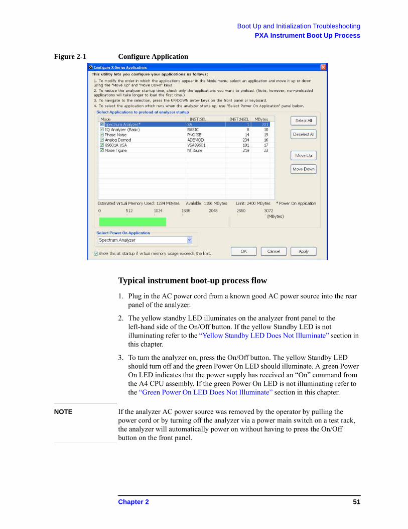
Boot Up and Initialization Troubleshooting
PXA Instrument Boot Up Process
Figure 2-1 Configure Application
Typical instrument boot-up process flow
1. Plug in the AC power cord from a known good AC power source into the rear panel of the analyzer.
2. The yellow standby LED illuminates on the analyzer front panel to the left-hand side of the On/Off button. If the yellow Standby LED is not illuminating refer to the “Yellow Standby LED Does Not Illuminate” section in this chapter.
3. To turn the analyzer on, press the On/Off button. The yellow Standby LED should turn off and the green Power On LED should illuminate. A green Power On LED indicates that the power supply has received an “On” command from the A4 CPU assembly. If the green Power On LED is not illuminating refer to the “Green Power On LED Does Not Illuminate” section in this chapter.
NOTE If the analyzer AC power source was removed by the operator by pulling the power cord or by turning off the analyzer via a power main switch on a test rack, the analyzer will automatically power on without having to press the On/Off button on the front panel.
Chapter 2 51
Boot Up and Initialization Troubleshooting
PXA Instrument Boot Up Process
4. The instrument fans should start running. The fans are mounted on the left-hand side of the analyzer and draw air into the instrument to cool the internal circuitry. If a fan is not running refer to the “Fan(s) Are Not Operating” section in this chapter.
5. The Agilent Technologies splash screen is displayed in white font on a dark background for ~5-10 seconds after the analyzer is turned on. If the Agilent Technologies logo is not displayed refer to the “No Agilent Splash Screen Displayed” section in this chapter. If the instrument hangs at the Agilent Technologies splash screen refer to the “Instrument Hangs at the Agilent Splash Screen” section in this chapter.
6. Verify text is displayed on screen where the user has the option of booting Windows XP or running the Agilent Recovery System. The default selection is to boot Windows XP. If a recovery is required, press the Down Arrow key on the front panel of the analyzer within 5 seconds to highlight “Agilent Recovery System” and press the Enter key on the analyzer, otherwise Windows XP will begin to boot. If the Windows XP boot screen is not displayed within a few seconds refer to the “Instrument Cannot Completely Load or Run the Operating System” section in this chapter.
7. If the recovery system is not selected the Windows XP Professional operating system will begin to boot up. This will take ~20-30 seconds.
NOTE If a recovery was selected follow the on-screen instructions and perform a system recovery. Additional information about performing a system recovery can be found in Chapter 9 , “CPU/Disk Drive Troubleshooting,” on page 279 in this manual.
8. The Agilent Technologies logo is displayed in white font on a blue background while Windows finishes loading user preferences. This can take up to 4 minutes. If this does not occur refer to the “Instrument Cannot Completely Load or Run the Operating System” section in this chapter.
9. By default, the initialization process of the PXA Spectrum Analyzer application begins loading. The N9030A PXA Signal Analyzer screen appears. This screen remains for slightly over 1 minute. If any of the initializing processes do not complete, refer to the “Initializations Did Not Complete” section in this chapter.
10.While the application software is loading the instrument will perform a number of internal alignments before the analyzer begins to sweep. A screen with a black background appears and the alignment progress is shown in a yellow box. The number of alignments is dependent on which hardware options are present. If an alignment fails, refer to the “Fails an Initial Alignment” section in this chapter.
52 Chapter 2
Boot Up and Initialization Troubleshooting
PXA Instrument Boot Up Process
11. If any of the initial alignments fail, check the alignment history for troubleshooting hints.
The instrument alignment history can be found at:
E:\AlignDataStorage\AlignmentHistory.txt
Look for any failed status for the various internal hardware items listed in this file.
Once the PXA application is fully initialized and aligned, the sweep should resemble Figure 2-2 when delivered from the factory. This completes the boot process from initial AC power to the spectrum analyzer application.
IMPORTANT If the power up state has been changed from the factory power on state by the user, the analyzer will boot to that state.
Figure 2-2 Typical Instrument Sweep at Power-up (Display theme changed for printing clarity)
Chapter 2 53
Boot Up and Initialization Troubleshooting
Potential Problems During Boot Process
Potential Problems During Boot Process
This section describes potential problems that may occur if there is an internal hardware issue that prohibits the instrument from completing a full boot up to the spectrum analyzer application.
Yellow Standby LED Does Not Illuminate
Control of the yellow front panel Standby LED comes from the A4 Processor board assembly. This signal is routed through the A7 Midplane board and is then buffered on the A8 Motherboard before being sent to the A1A2 Front Panel Interface board through W1. Of course, the power for this all originates with the A6 Power Supply Assembly. When the Standby LED does not come on it could be due to any one of these assemblies. This procedure will help to determine which one is the cause.
If the instrument turns on and operates properly but the yellow Standby LED does not work then all that will need to be done is to trace where the control signal for the LED is being lost using the routing information in the preceding paragraph.
1. The Standby LED will only turn on when the instrument is connected to an AC power source that has a voltage level and frequency of that specified for the instrument. Before proceeding verify that these requirements are being met. Refer to the instrument rear panel for these requirements.
2. Remove the AC power cord and then remove the instrument cover. Refer to Chapter 16, “Assembly Replacement Procedures,” on page 427 in this manual.
3. Referring to Figure 2-3, verify the +5.1VSB LED on the A7 Midplane board is on (green).
Figure 2-3 A7 Midplane Board +5.1VSB LED
54 Chapter 2
Boot Up and Initialization Troubleshooting
Potential Problems During Boot Process
NOTE Most DC power supplies come from the A6 Power Supply assembly. However, the most convenient measurement location for all the DC supplies is the A7 Midplane. All power supply LED's are accessible once the instrument cover has been removed.
Is the +5.1VSB LED on the A7 Midplane board on?
If yes:
After verifying that the connections from the yellow front panel Standby LED back to the A4 Processor board are not at fault, replace the A4 Processor board.
If not:
Replace the A6 Power Supply assembly.
NOTE Before replacing the power supply, verify the midplane and motherboard interconnects are mechanically secure.
Chapter 2 55
Boot Up and Initialization Troubleshooting
Potential Problems During Boot Process
Green Power On LED Does Not Illuminate
Control of the green front panel Power On LED comes from the A4 Processor board assembly. This signal is routed through the A7 Midplane board and is then buffered on the A8 Motherboard before being sent to the A1A2 Front Panel Interface board through W1. Of course, the power for this all originates with the A6 Power Supply Assembly. When the Power On LED does not come on it could be due to any one of these assemblies. This procedure will help to determine which one is the cause.
This procedure assumes that the yellow Standby LED does turn on when the AC power is connected to the rear panel of the instrument. If it doesn't, refer to the “Yellow Standby LED Does Not Illuminate” section before proceeding.
If the instrument turns on and operates properly but the green Power On LED does not work then all that will need to be done is to trace where the control signal for the LED is being lost using the routing information in the preceding paragraph.
1. The Power On LED will only turn on when the instrument is connected to an AC power source that has a voltage level and frequency of that specified for the instrument and the front panel On/Off button has been pressed. Before proceeding verify that these requirements are being met. Refer to the instrument rear panel for these requirements.
2. Remove the AC power cord and then remove the instrument cover. Refer to Chapter 16, “Assembly Replacement Procedures,” on page 427 in this manual.
3. Remove the Top Brace. Refer to Chapter 16, “Assembly Replacement Procedures,” on page 427 in this manual.
4. With AC power connected to the rear of the instrument but without turning it on, leaving it in standby mode, measure the voltage at Test Point 518 (POWER_ON_L) of the A7 Midplane board assembly. See Figure 2-4 for Test Point 518 location.
Does the voltage at Test Point 518 measure 5 VDC?
If yes:
Proceed to step 5.
If not:
Replace the A6 Power Supply assembly.
NOTE Before replacing the power supply, verify the midplane and motherboard interconnects are mechanically secure.
56 Chapter 2
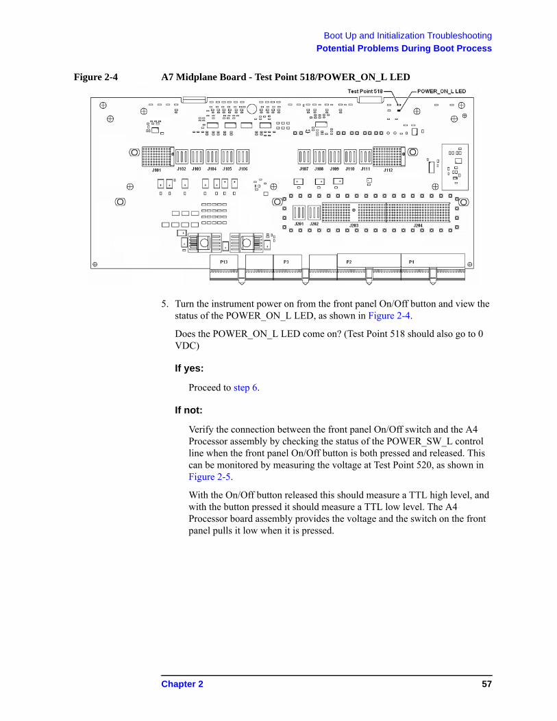
Boot Up and Initialization Troubleshooting
Potential Problems During Boot Process
Figure 2-4 A7 Midplane Board - Test Point 518/POWER_ON_L LED
5. Turn the instrument power on from the front panel On/Off button and view the status of the POWER_ON_L LED, as shown in Figure 2-4.
Does the POWER_ON_L LED come on? (Test Point 518 should also go to 0 VDC)
If yes:
Proceed to step 6.
If not:
Verify the connection between the front panel On/Off switch and the A4 Processor assembly by checking the status of the POWER_SW_L control line when the front panel On/Off button is both pressed and released. This can be monitored by measuring the voltage at Test Point 520, as shown in Figure 2-5.
With the On/Off button released this should measure a TTL high level, and with the button pressed it should measure a TTL low level. The A4 Processor board assembly provides the voltage and the switch on the front panel pulls it low when it is pressed.
Chapter 2 57
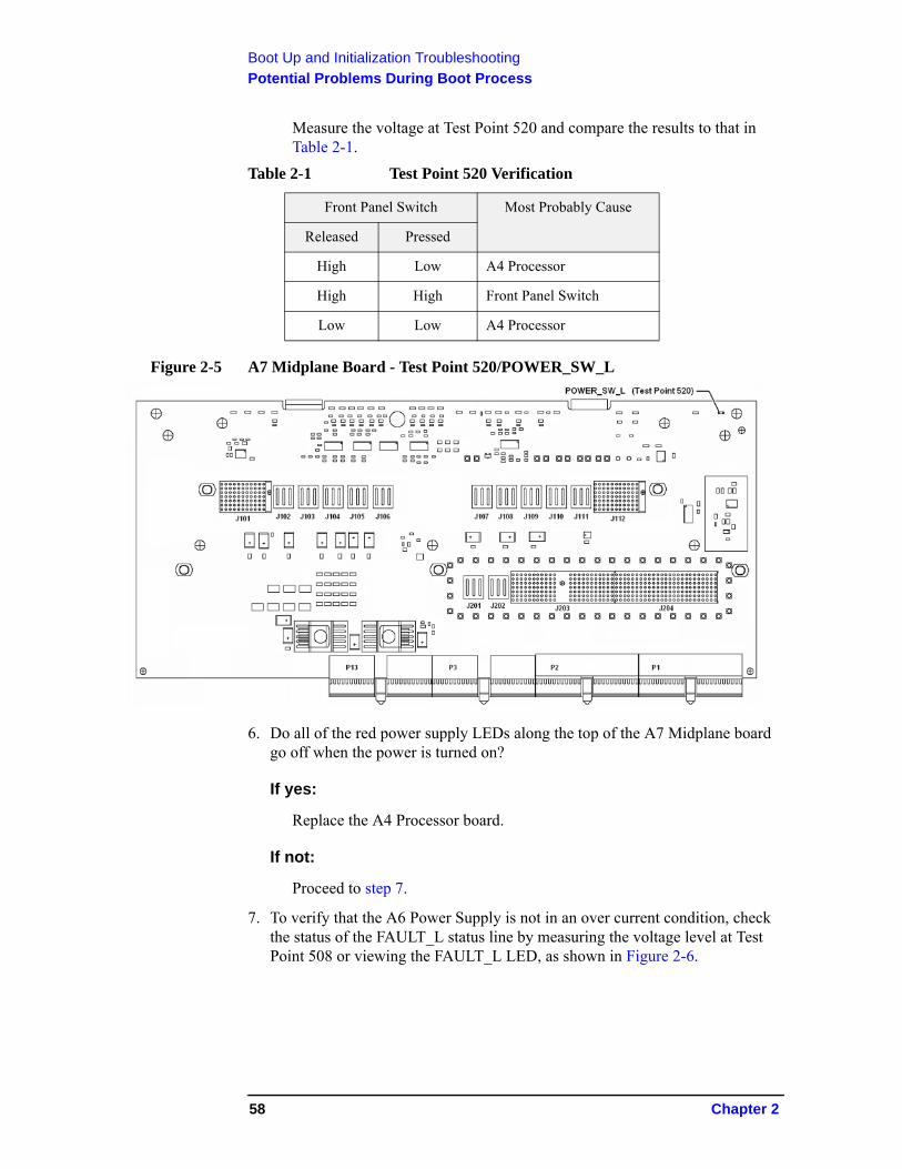
Boot Up and Initialization Troubleshooting
Potential Problems During Boot Process
Measure the voltage at Test Point 520 and compare the results to that in Table 2-1.
Figure 2-5 A7 Midplane Board - Test Point 520/POWER_SW_L
6. Do all of the red power supply LEDs along the top of the A7 Midplane board go off when the power is turned on?
If yes:
Replace the A4 Processor board.
If not:
Proceed to step 7.
7. To verify that the A6 Power Supply is not in an over current condition, check the status of the FAULT_L status line by measuring the voltage level at Test Point 508 or viewing the FAULT_L LED, as shown in Figure 2-6.
Table 2-1 Test Point 520 Verification
Front Panel Switch Most Probably Cause
Released Pressed
High Low A4 Processor
High High Front Panel Switch
Low Low A4 Processor
58 Chapter 2
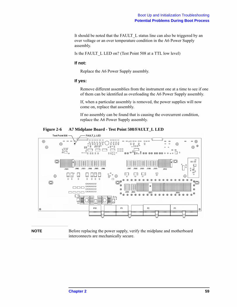
Boot Up and Initialization Troubleshooting
Potential Problems During Boot Process
It should be noted that the FAULT_L status line can also be triggered by an over voltage or an over temperature condition in the A6 Power Supply assembly.
Is the FAULT_L LED on? (Test Point 508 at a TTL low level)
If not:
Replace the A6 Power Supply assembly.
If yes:
Remove different assemblies from the instrument one at a time to see if one of them can be identified as overloading the A6 Power Supply assembly.
If, when a particular assembly is removed, the power supplies will now come on, replace that assembly.
If no assembly can be found that is causing the overcurrent condition, replace the A6 Power Supply assembly.
Figure 2-6 A7 Midplane Board - Test Point 508/FAULT_L LED
NOTE Before replacing the power supply, verify the midplane and motherboard interconnects are mechanically secure.
Chapter 2 59
Boot Up and Initialization Troubleshooting
Potential Problems During Boot Process
Fan(s) Are Not Operating
Control of the instrument fans comes from the A6 Power Supply assembly. This signal is routed from the A6 Power Supply through the A7 Midplane board, where there is a test point and LED to monitor the level, and is then routed to the A8 Motherboard where it is filtered before being sent to the Fans. When the Fans do not come on it could be due to any one of these assemblies. This procedure will help to determine which one is the cause.
This procedure assumes that the green Power On LED on the front panel does turn on when the instrument is turned on. If it doesn't, refer to the “Green Power On LED Does Not Illuminate” section before proceeding.
1. The instrument fans will only turn on when the instrument is connected to an AC power source that has a voltage level and frequency of that specified for the instrument and the front panel On/Off button has been pressed. Before proceeding verify that these requirements are being met. Refer to the instrument rear panel for these requirements.
2. Remove the AC power cord and then remove the instrument cover. Refer to Chapter 16, “Assembly Replacement Procedures,” on page 427 in this manual.
3. Are all three fans not spinning?
If yes:
Proceed to step 4.
If not:
Proceed to step 6.
4. Remove the Top Brace. Refer to Chapter 16, “Assembly Replacement Procedures,” on page 427 in this manual.
60 Chapter 2
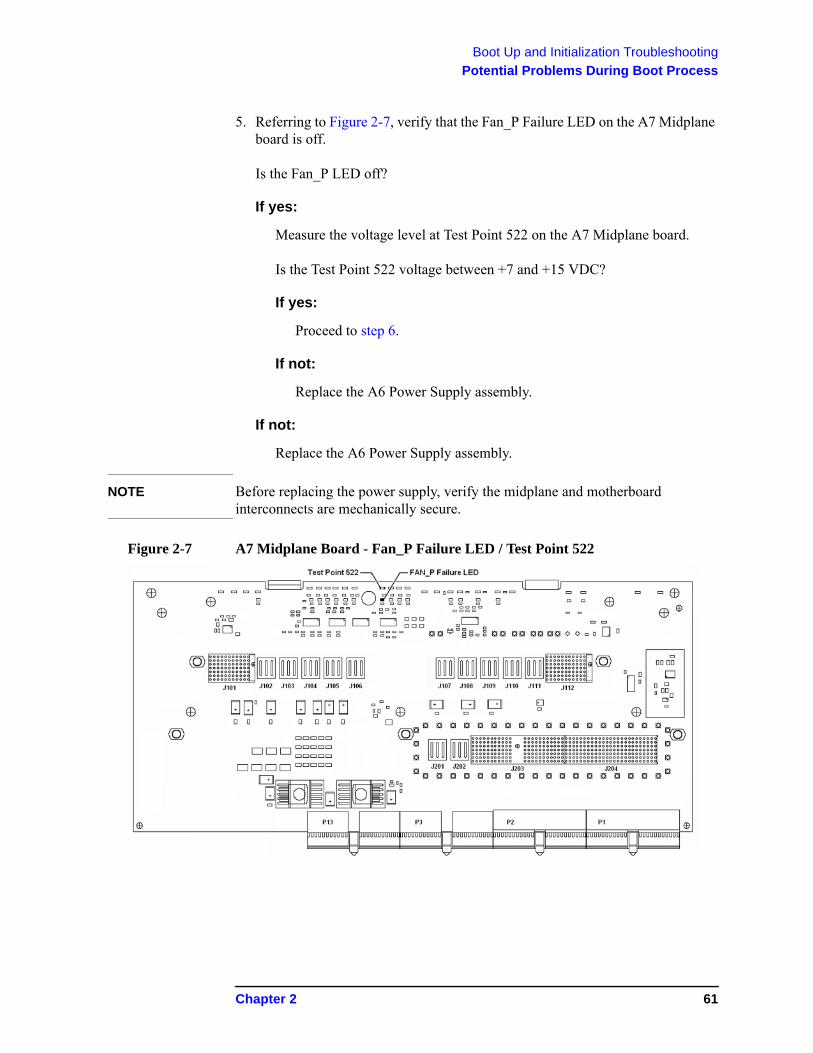
Boot Up and Initialization Troubleshooting
Potential Problems During Boot Process
5. Referring to Figure 2-7, verify that the Fan_P Failure LED on the A7 Midplane board is off.
Is the Fan_P LED off?
If yes:
Measure the voltage level at Test Point 522 on the A7 Midplane board.
Is the Test Point 522 voltage between +7 and +15 VDC?
If yes:
Proceed to step 6.
If not:
Replace the A6 Power Supply assembly.
If not:
Replace the A6 Power Supply assembly.
NOTE Before replacing the power supply, verify the midplane and motherboard interconnects are mechanically secure.
Figure 2-7 A7 Midplane Board - Fan_P Failure LED / Test Point 522
Chapter 2 61
Boot Up and Initialization Troubleshooting
Potential Problems During Boot Process
6. With the instrument turned off, and the AC power cord removed, remove the Fan Assembly including unplugging all fans from the A8 Motherboard. Refer to Chapter 16, “Assembly Replacement Procedures,” on page 427 in this manual.
7. Turn the instrument power back on and measure the fan voltage at all three of the fan connectors (J6, J7, & J8) on the A8 Motherboard.
Each connector has three pins. The outer conductors on all connectors are the FAN_P supply and the center conductors are FAN_N. The voltage between FAN_P and chassis ground should be between +7 and +15 VDC on all three connectors.
Does the A8 Motherboard fan connector for the fan(s) that do not work have the required voltage level?
If yes:
Replace the fan(s) that is not working
If not:
After verifying that the connections between the A7 Midplane board and the A8 Motherboard are mechanically and electrically secure replace the A8 Motherboard.
No Agilent Splash Screen Displayed
(Black background with white “Agilent Technologies” text)
A problem of not displaying the Agilent splash screen could be caused by many different things. It could be due to a down power supply, a processor hardware problem, an instrument boot-up process error, a display section failure, etc.
This procedure assumes that the green Power On LED on the front panel does turn on when the instrument is turned on. If it doesn't, refer to the “Green Power On LED Does Not Illuminate” section before proceeding.
1. Remove the AC power cord and then remove the instrument cover. Refer to Chapter 16, “Assembly Replacement Procedures,” on page 427 in this manual.
2. Remove the Top Brace. Refer to Chapter 16, “Assembly Replacement Procedures,” on page 427 in this manual.
3. With the AC power applied and the On/Off button turned on, verify that all of the power supply voltages are at their proper level. This can easily be done by viewing the power supply LEDs on the back side of the A7 Midplane board. Refer to the "A7 Midplane Board Assembly Troubleshooting" on page 312.
62 Chapter 2
Boot Up and Initialization Troubleshooting
Potential Problems During Boot Process
Are all of the power supply voltages at the proper level?
If yes:
Proceed to step 4.
If not:
After verifying that the connections between the A6 Power Supply, the A7 Midplane board, and the A8 Motherboard are all mechanically and electrically secure, replace the A6 Power Supply assembly.
4. Connect an external VGA monitor to the rear panel display output.
Does the external monitor display the correct information?
If yes:
Proceed to the “Troubleshooting a Blank Display” section in this chapter.
If not:
Replace the A4 Processor Board assembly.
Chapter 2 63
Boot Up and Initialization Troubleshooting
Potential Problems During Boot Process
Instrument Hangs at the Agilent Splash Screen
A problem of the instrument hanging at the Agilent splash screen could be caused by many different things. It could be due to a down power supply, a processor hardware problem, an instrument boot-up process error, etc.
1. Remove the AC power cord and then remove the instrument cover. Refer to Chapter 16, “Assembly Replacement Procedures,” on page 427 in this manual.
2. Remove the Top Brace. Refer to Chapter 16, “Assembly Replacement Procedures,” on page 427 in this manual.
3. With the AC power applied and the On/Off button turned on, verify that all of the power supply voltages are at their proper level. This can easily be done by viewing the power supply LEDs on the back side of the A7 Midplane board. See the "A7 Midplane Board Assembly Troubleshooting" on page 312.
Are all of the power supply voltages at the proper level?
If yes:
After verifying that the connections from the A7 Midplane board to the A4 Processor board are not at fault, replace the A4 Processor board.
If not:
After verifying that the connections between the A6 Power Supply, the A7 Midplane board, and the A8 Motherboard are all mechanically and electrically secure, replace the A6 Power Supply assembly.
64 Chapter 2
Boot Up and Initialization Troubleshooting
Potential Problems During Boot Process
Instrument Cannot Completely Load or Run the Operating System
A problem of the instrument not loading the operating system can be caused by a few different things. It could be due to a down power supply, a processor hardware problem, an instrument boot-up process error, corrupt disk drive, etc.
This procedure assumes that the instrument can get past the Agilent splash screen at power on. If it doesn't, refer to the “Instrument Hangs at the Agilent Splash Screen” section before proceeding.
1. Verify that there are no external USB storage devices connected to the instrument.
2. Does the instrument get far enough along in the boot process to run the “Agilent Recovery System”?
If yes:
Run the Agilent Recovery System by referring to the “Disk Drive Recovery Process” on page 298. If this does not correct the problem replace the A5 Disk Drive.
If not:
Replace the A5 Disk Drive.
Troubleshooting a Blank Display
This section is intended to troubleshoot a display system problem that would cause the internal LCD to be blank. It is assumed that the rest of the instrument is booting up and functioning properly. To determine if the problem is an internal display issue only, connect an external VGA monitor to the rear panel display output. If the rear panel display output is also not working go to the “No Agilent Splash Screen Displayed” section in this chapter.
Once it has been determined that the rest of the instrument appears to be functioning properly there are a few possible problems that could be causing the display to be blank. They are:
• An LCD Backlight inverter problem
• A video signal path integrity problem
• A video controller / LCD problem
Chapter 2 65
Boot Up and Initialization Troubleshooting
Potential Problems During Boot Process
Verify LCD Backlight Functionality
There are two backlights within the LCD assembly, one across the top and one across the bottom. If only one of the backlights has burnt out, the other will still function. Considering this fact, as well as the fact that the expected life span of the backlights is much longer than the LCD itself, it is not very likely that the backlights themselves would cause a completely blank display.
To determine if a blank display problem is backlight related:
1. Remove the AC power cord and then remove the instrument cover. Refer to Chapter 16, “Assembly Replacement Procedures,” on page 427 in this manual.
2. Remove the Top Brace. Refer to Chapter 16, “Assembly Replacement Procedures,” on page 427 in this manual.
3. Turn the instrument on and allow enough time for it to completely boot-up.
4. Shine a bright light at the display and look closely for the expected information (a large flashlight should work). Since most of the display section of the screen has a black background you will need to look at either the area next to the softkeys or the area across the top of the screen, since these sections will have the largest areas of lighter information in them.
5. Can the expected display information now be seen?
If yes:
The problem is backlight related. Proceed to step 6.
If not:
The problem is not backlight related. Skip to “Verify Video Signal Path Integrity”.
66 Chapter 2
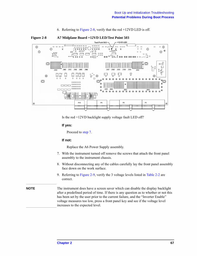
Boot Up and Initialization Troubleshooting
Potential Problems During Boot Process
6. Referring to Figure 2-8, verify that the red +12VD LED is off.
Figure 2-8 A7 Midplane Board +12VD LED/Test Point 503
Is the red +12VD backlight supply voltage fault LED off?
If yes:
Proceed to step 7.
If not:
Replace the A6 Power Supply assembly.
7. With the instrument turned off remove the screws that attach the front panel assembly to the instrument chassis.
8. Without disconnecting any of the cables carefully lay the front panel assembly face down on the work surface.
9. Referring to Figure 2-9, verify the 3 voltage levels listed in Table 2-2 are correct.
NOTE The instrument does have a screen saver which can disable the display backlight after a predefined period of time. If there is any question as to whether or not this has been set by the user prior to the current failure, and the “Inverter Enable” voltage measures too low, press a front panel key and see if the voltage level increases to the expected level.
Chapter 2 67
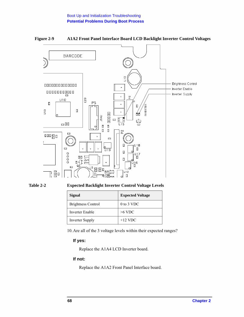
Boot Up and Initialization Troubleshooting
Potential Problems During Boot Process
Figure 2-9 A1A2 Front Panel Interface Board LCD Backlight Inverter Control Voltages
10.Are all of the 3 voltage levels within their expected ranges?
If yes:
Replace the A1A4 LCD Inverter board.
If not:
Replace the A1A2 Front Panel Interface board.
Table 2-2 Expected Backlight Inverter Control Voltage Levels
Signal Expected Voltage
Brightness Control 0 to 3 VDC
Inverter Enable >6 VDC
Inverter Supply +12 VDC
68 Chapter 2
Boot Up and Initialization Troubleshooting
Potential Problems During Boot Process
Verify Video Signal Path Integrity
The video controller is located on the A4 Processor assembly and is routed to the front panel LCD through a few interconnections. These interconnections are:
• A4 Processor assembly to A7 Midplane Board
• A7 Midplane Board to A8 Motherboard assembly
• A8 Motherboard assembly to A1A2 Front Panel Interface assembly via W1 ribbon cable
• A1A2 Front Panel Interface to A1A3 LCD via A1W1 flex-circuit
If all of these connections are properly made and none of the cables are damaged proceed to “Video Controller / LCD Troubleshooting”.
Video Controller / LCD Troubleshooting
The video controller is located on the A4 Processor assembly. The video signals that the controller outputs are LVDS. As described above, these signals are routed to the LCD via the A7 Midplane Board, A8 Motherboard, and A1A2 Front Panel Interface board.
On the A1A2 Front Panel Interface board the LVDS signals are buffered and then sent to the LCD via the A1W1 Flex circuit.
The most likely cause for a video problem is the A4 Processor assembly; however it could be the result of a defective LCD.
Initializations Did Not Complete
During the initialization of the PXA Signal Analyzer Application the following messages will be displayed on the application splash screen:
• Checking for required services (1 of 7)• Initializing License Services (2 of 7)• Initializing Hardware (3 of 7)• Initializing Data Services (4 of 7)• Initializing SCPI Services (5 of 7)• Initializing Message Services (6 of 7)• Initializing Front Panel EEPROM Services (7 of 7)
If there is a problem with any of these initializations not completing or causing an error message to be displayed refer to the instrument Event Log. This can be accessed by using an external USB keyboard and mouse and selecting Start, Run, enter Eventvwr.exe, and select OK.
Once the Event Viewer comes up, look under SA for the latest error entries. Double-click on the entries to view further details, which should give you some idea of what the problem is.
Chapter 2 69
Boot Up and Initialization Troubleshooting
Potential Problems During Boot Process
Fails an Initial Alignment
Troubleshooting Alignment Failures Using the Alignment History Screen
At instrument power on, an initial alignment is automatically performed. It is also possible to manually trigger an alignment by pressing System, Alignments, Align Now, All. The power on alignment performs a few more alignments than the manual Align Now All routine.
The number of alignments depends on the hardware options present in the signal analyzer.
Using an external USB keyboard and mouse, access the alignment history, which can be found in a text file at:
E:AlignDataStorage\AlignmentHistory.txt
You will find the most current alignment information at the bottom of this file. Look for the failed alignments. From the windows task bar you can click Edit, Find and type in FAILED and search for a failure.
Note that the information in the history file usually shows that multiple measurements are made for a given alignment routine, and measured values with upper and lower limits are given. For example, the Mechanical Attenuator Algorithm measures and displays all of the attenuator step values. In this case, you can view which steps fail, and by how much. Then based on the input attenuator drawing on the PXA RF Block Diagram, you can determine which attenuator steps are available on each of the two input attenuators. Then you can view the troubleshooting information for the Front End Controller or deduce from the attenuator steps that fail, which attenuator is faulty.
WARNING Assure there is no 50 MHz signal above 0 dBm applied to the signal analyzer input when the alignment routine is performed. This can cause errors.
The description of the alignment and the alignment hardware dependencies are listed in Table 2-3.
70 Chapter 2
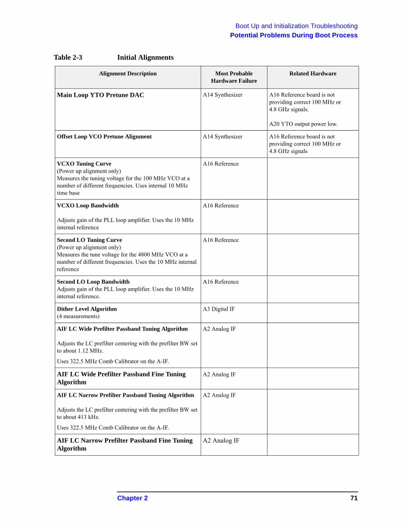
Boot Up and Initialization Troubleshooting
Potential Problems During Boot Process
Table 2-3 Initial Alignments
Alignment Description Most Probable Hardware Failure
Related Hardware
Main Loop YTO Pretune DAC A14 Synthesizer A16 Reference board is not providing correct 100 MHz or 4.8 GHz signals.
A20 YTO output power low.
Offset Loop VCO Pretune Alignment A14 Synthesizer A16 Reference board is not providing correct 100 MHz or 4.8 GHz signals
VCXO Tuning Curve(Power up alignment only)Measures the tuning voltage for the 100 MHz VCO at a number of different frequencies. Uses internal 10 MHz time base
A16 Reference
VCXO Loop Bandwidth
Adjusts gain of the PLL loop amplifier. Uses the 10 MHz internal reference
A16 Reference
Second LO Tuning Curve(Power up alignment only)Measures the tune voltage for the 4800 MHz VCO at a number of different frequencies. Uses the 10 MHz internal reference
A16 Reference
Second LO Loop BandwidthAdjusts gain of the PLL loop amplifier. Uses the 10 MHz internal reference.
A16 Reference
Dither Level Algorithm(4 measurements)
A3 Digital IF
AIF LC Wide Prefilter Passband Tuning Algorithm
Adjusts the LC prefilter centering with the prefilter BW set to about 1.12 MHz.
Uses 322.5 MHz Comb Calibrator on the A-IF.
A2 Analog IF
AIF LC Wide Prefilter Passband Fine Tuning Algorithm
A2 Analog IF
AIF LC Narrow Prefilter Passband Tuning Algorithm
Adjusts the LC prefilter centering with the prefilter BW set to about 413 kHz.
Uses 322.5 MHz Comb Calibrator on the A-IF.
A2 Analog IF
AIF LC Narrow Prefilter Passband Fine Tuning Algorithm
A2 Analog IF
Chapter 2 71
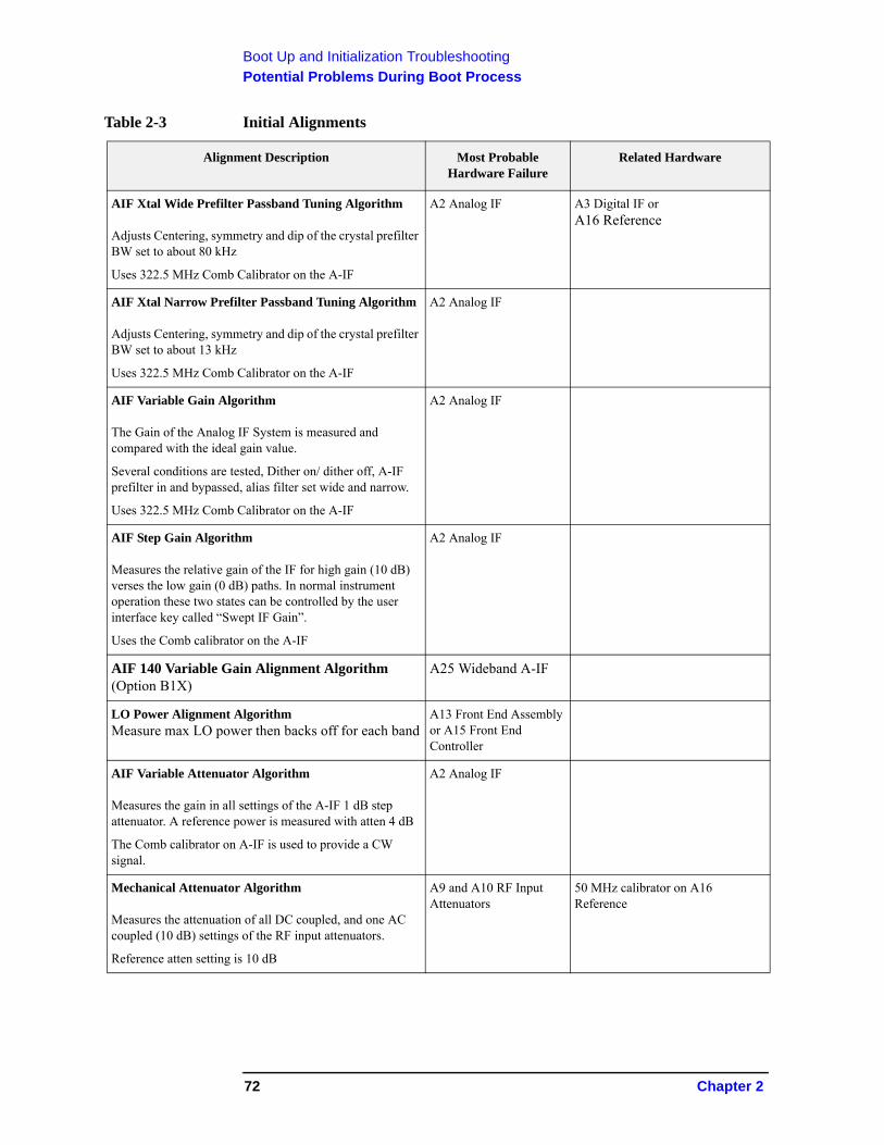
Boot Up and Initialization Troubleshooting
Potential Problems During Boot Process
AIF Xtal Wide Prefilter Passband Tuning Algorithm
Adjusts Centering, symmetry and dip of the crystal prefilter BW set to about 80 kHz
Uses 322.5 MHz Comb Calibrator on the A-IF
A2 Analog IF A3 Digital IF or A16 Reference
AIF Xtal Narrow Prefilter Passband Tuning Algorithm
Adjusts Centering, symmetry and dip of the crystal prefilter BW set to about 13 kHz
Uses 322.5 MHz Comb Calibrator on the A-IF
A2 Analog IF
AIF Variable Gain Algorithm
The Gain of the Analog IF System is measured and compared with the ideal gain value.
Several conditions are tested, Dither on/ dither off, A-IF prefilter in and bypassed, alias filter set wide and narrow.
Uses 322.5 MHz Comb Calibrator on the A-IF
A2 Analog IF
AIF Step Gain Algorithm
Measures the relative gain of the IF for high gain (10 dB) verses the low gain (0 dB) paths. In normal instrument operation these two states can be controlled by the user interface key called “Swept IF Gain”.
Uses the Comb calibrator on the A-IF
A2 Analog IF
AIF 140 Variable Gain Alignment Algorithm(Option B1X)
A25 Wideband A-IF
LO Power Alignment AlgorithmMeasure max LO power then backs off for each band
A13 Front End Assembly or A15 Front End Controller
AIF Variable Attenuator Algorithm
Measures the gain in all settings of the A-IF 1 dB step attenuator. A reference power is measured with atten 4 dB
The Comb calibrator on A-IF is used to provide a CW signal.
A2 Analog IF
Mechanical Attenuator Algorithm
Measures the attenuation of all DC coupled, and one AC coupled (10 dB) settings of the RF input attenuators.
Reference atten setting is 10 dB
A9 and A10 RF Input Attenuators
50 MHz calibrator on A16 Reference
Table 2-3 Initial Alignments
Alignment Description Most Probable Hardware Failure
Related Hardware
72 Chapter 2
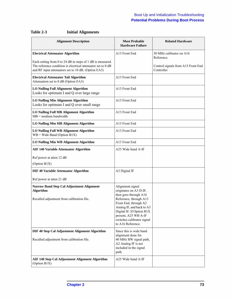
Boot Up and Initialization Troubleshooting
Potential Problems During Boot Process
Electrical Attenuator Algorithm
Each setting from 0 to 24 dB in steps of 1 dB is measured. The reference condition is electrical attenuator set to 0 dB and RF input attenuators set to 10 dB. (Option EA3)
A13 Front End 50 MHz calibrator on A16 Reference.
Control signals from A15 Front End Controller
Electrical Attenuator Tail Algorithm Attenuation set to 0 dB (Option EA3)
A13 Front End
LO Nulling Full Alignment AlgorithmLooks for optimum I and Q over large range
A13 Front End
LO Nulling Min Alignment AlgorithmLooks for optimum I and Q over small range
A13 Front End
LO Nulling Full MB Alignment AlgorithmMB = medium bandwidth
A13 Front End
LO Nulling Min MB Alignment Algorithm A13 Front End
LO Nulling Full WB Alignment AlgorithmWB = Wide Band (Option B1X)
A13 Front End
LO Nulling Min WB Alignment Algorithm A13 Front End
AIF 140 Variable Attenuator Algorithm
Ref power at atten 12 dB
(Option B1X)
A25 Wide band A-IF
DIF 40 Variable Attenuator Algorithm
Ref power at atten 21 dB
A3 Digital IF
Narrow Band Step Cal Adjustment Alignment Algorithm
Recalled adjustment from calibration file.
Alignment signal originates on A3 D-IF, then goes through A16 Reference, through A13 Front End, through A2 Analog IF, and back to A3 Digital IF. If Option B1X present, A25 WB A-IF switches calibrator signal to A16 Reference.
DIF 40 Step Cal Adjustment Alignment Algorithm
Recalled adjustment from calibration file.
Since this is wide band alignment done for 40 MHz BW signal path, A2 Analog IF is not included in the signal path.
AIF 140 Step Cal Adjustment Alignment Algorithm(Option B1X)
A25 Wide band A-IF
Table 2-3 Initial Alignments
Alignment Description Most Probable Hardware Failure
Related Hardware
Chapter 2 73
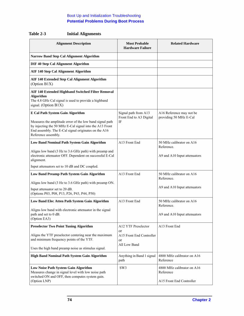
Boot Up and Initialization Troubleshooting
Potential Problems During Boot Process
Narrow Band Step Cal Alignment Algorithm
DIF 40 Step Cal Alignment Algorithm
AIF 140 Step Cal Alignment Algorithm
AIF 140 Extended Step Cal Alignment Algorithm (Option B1X)
AIF 140 Extended Highband Switched Filter Removal AlgorithmThe 4.8 GHz Cal signal is used to provide a highband signal. (Option B1X)
E Cal Path System Gain Algorithm
Measures the amplitude error of the low band signal path by injecting the 50 MHz E-Cal signal into the A13 Front End assembly. The E-Cal signal originates on the A16 Reference assembly.
Signal path from A13 Front End to A3 Digital IF
A16 Reference may not be providing 50 MHz E-Cal
Low Band Nominal Path System Gain Algorithm
Aligns low band (3 Hz to 3.6 GHz path) with preamp and electronic attenuator OFF. Dependent on successful E-Cal alignment.
Input attenuators set to 10 dB and DC coupled.
A13 Front End 50 MHz calibrator on A16 Reference.
A9 and A10 Input attenuators
Low Band Preamp Path System Gain Algorithm
Aligns low band (3 Hz to 3.6 GHz path) with preamp ON.
Input attenuator set to 20 dB.(Options P03, P08, P13, P26, P43, P44, P50)
A13 Front End 50 MHz calibrator on A16 Reference.
A9 and A10 Input attenuators
Low Band Elec Atten Path System Gain Algorithm
Aligns low band with electronic attenuator in the signal path and set to 0 dB.(Option EA3)
A13 Front End 50 MHz calibrator on A16 Reference.
A9 and A10 Input attenuators
Preselector Two Point Tuning Algorithm
Aligns the YTF preselector centering near the maximum and minimum frequency points of the YTF.
Uses the high band preamp noise as stimulus signal.
A12 YTF PreselectororA15 Front End ControllerorAll Low Band
A13 Front End
High Band Nominal Path System Gain Algorithm Anything in Band 1 signal path
4800 MHz calibrator on A16 Reference
Low Noise Path System Gain AlgorithmMeasures change in signal level with low noise path switched ON and OFF, then computes system gain.(Option LNP)
SW3 4800 MHz calibrator on A16 Reference
A15 Front End Controller
Table 2-3 Initial Alignments
Alignment Description Most Probable Hardware Failure
Related Hardware
74 Chapter 2
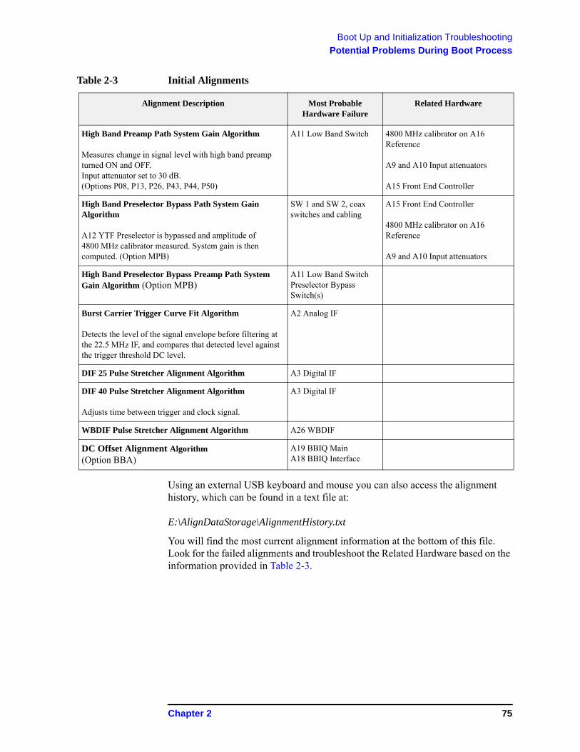
Boot Up and Initialization Troubleshooting
Potential Problems During Boot Process
Using an external USB keyboard and mouse you can also access the alignment history, which can be found in a text file at:
E:\AlignDataStorage\AlignmentHistory.txt
You will find the most current alignment information at the bottom of this file. Look for the failed alignments and troubleshoot the Related Hardware based on the information provided in Table 2-3.
High Band Preamp Path System Gain Algorithm
Measures change in signal level with high band preamp turned ON and OFF.Input attenuator set to 30 dB.(Options P08, P13, P26, P43, P44, P50)
A11 Low Band Switch 4800 MHz calibrator on A16 Reference
A9 and A10 Input attenuators
A15 Front End Controller
High Band Preselector Bypass Path System Gain Algorithm
A12 YTF Preselector is bypassed and amplitude of 4800 MHz calibrator measured. System gain is then computed. (Option MPB)
SW 1 and SW 2, coax switches and cabling
A15 Front End Controller
4800 MHz calibrator on A16 Reference
A9 and A10 Input attenuators
High Band Preselector Bypass Preamp Path System Gain Algorithm (Option MPB)
A11 Low Band SwitchPreselector Bypass Switch(s)
Burst Carrier Trigger Curve Fit Algorithm
Detects the level of the signal envelope before filtering at the 22.5 MHz IF, and compares that detected level against the trigger threshold DC level.
A2 Analog IF
DIF 25 Pulse Stretcher Alignment Algorithm A3 Digital IF
DIF 40 Pulse Stretcher Alignment Algorithm
Adjusts time between trigger and clock signal.
A3 Digital IF
WBDIF Pulse Stretcher Alignment Algorithm A26 WBDIF
DC Offset Alignment Algorithm(Option BBA)
A19 BBIQ MainA18 BBIQ Interface
Table 2-3 Initial Alignments
Alignment Description Most Probable Hardware Failure
Related Hardware
Chapter 2 75
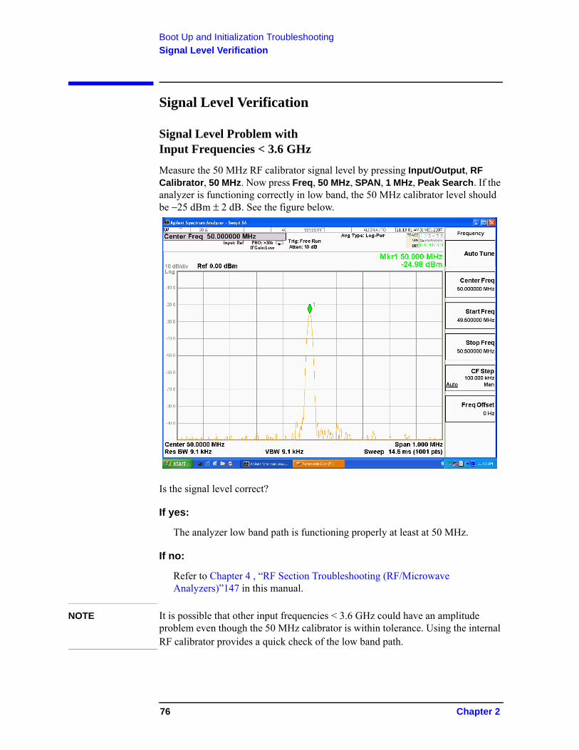
Boot Up and Initialization Troubleshooting
Signal Level Verification
Signal Level Verification
Signal Level Problem with Input Frequencies < 3.6 GHz
Measure the 50 MHz RF calibrator signal level by pressing Input/Output, RF Calibrator, 50 MHz. Now press Freq, 50 MHz, SPAN, 1 MHz, Peak Search. If the analyzer is functioning correctly in low band, the 50 MHz calibrator level should be −25 dBm ± 2 dB. See the figure below.
Is the signal level correct?
If yes:
The analyzer low band path is functioning properly at least at 50 MHz.
If no:
Refer to Chapter 4 , “RF Section Troubleshooting (RF/Microwave Analyzers)”147 in this manual.
NOTE It is possible that other input frequencies < 3.6 GHz could have an amplitude problem even though the 50 MHz calibrator is within tolerance. Using the internal RF calibrator provides a quick check of the low band path.
76 Chapter 2
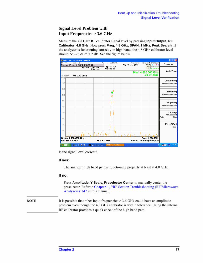
Boot Up and Initialization Troubleshooting
Signal Level Verification
Signal Level Problem with Input Frequencies > 3.6 GHz
Measure the 4.8 GHz RF calibrator signal level by pressing Input/Output, RF Calibrator, 4.8 GHz. Now press Freq, 4.8 GHz, SPAN, 1 MHz, Peak Search. If the analyzer is functioning correctly in high band, the 4.8 GHz calibrator level should be −28 dBm ± 2 dB. See the figure below.
Is the signal level correct?
If yes:
The analyzer high band path is functioning properly at least at 4.8 GHz.
If no:
Press Amplitude, Y-Scale, Preselector Center to manually center the preselector. Refer to Chapter 4 , “RF Section Troubleshooting (RF/Microwave Analyzers)”147 in this manual.
NOTE It is possible that other input frequencies > 3.6 GHz could have an amplitude problem even though the 4.8 GHz calibrator is within tolerance. Using the internal RF calibrator provides a quick check of the high band path.
Chapter 2 77

Boot Up and Initialization Troubleshooting
Signal Level Verification
78 Chapter 2
3 Instrument Messages
79
Instrument Messages
Introduction
Introduction
The Error and Status messaging system of the Agilent Signal Analyzer reports events and conditions in a consistent fashion, as well as logging and reporting event history.
Event vs. Condition Messages
An Event is simply a message indicating that something has happened. Events are sub-divided according to their severity, into Error, Warning or Advisory categories. The sub-divisions are described in more detail in the section “Event and Condition Categories”.
Event messages appear in the Message Line at the bottom left of the analyzer’s display window.
A Condition is a state of the Analyzer, which is characterized by a Detection event and a Clearing event. Conditions may be Errors or Warnings.
Condition messages appear in the Status Panel at the bottom right of the analyzer’s display screen.
Event and Condition Categories
The three categories of severity are described below, for both Events and Conditions.
Errors Error messages appear when a requested operation has failed. (For example, “Detector not available”, “File not saved”.) Error messages are often generated during remote operation when an invalid programming command has been entered. (For example, “Undefined header”.)
Some errors are conditions rather than single events. They exist for a period of time, so they have associated “Detected” and “Cleared” events. (For example, “LO Unlocked” or “External reference out of range”)
Error messages appear in the Status Panel at the bottom of the display. A message remains until you press a key, or another message is displayed in its place.
Error messages are logged in the error queues. If the error is a condition, both the Detected and Cleared events are logged.
80 Chapter 3
Instrument Messages
Introduction
Event Message Format
The event messages are listed in numerical order according to their message number. Advisory messages do not have numbers, and are listed in alphabetical order.
An explanation is included with each error to further clarify its meaning. Some errors are specified in industry standards and there are references to the IEEE
Warnings Warning messages appear when a requested operation has completed successfully, but there are modifications and/or side effects. (For example, if you requested too high a stop frequency, then “Data out of range” is displayed and the analyzer sets itself to the highest available stop frequency.)
Some warnings are conditions rather than single events. They exist for a period of time, so they have a “Detected” event and a “Cleared” event. (For example, if you set the sweep time too fast for a measurement to meet the instrument specifications then the “Meas Uncal” message is displayed until you slow down the sweep time.)
Warning messages appear in the Status Panel at the bottom of the display. The message remains until you press a key, or another message is displayed in its place.
Warnings are logged in the error queues. If the warning is a condition, both the Detected and Cleared event messages are logged.
Advisories Advisory messages tell the front panel user some useful information. (For example, “File saved successfully” or “Measuring the fundamental”.)
Advisory messages appear in the Status Panel at the bottom of the display. The message remains until you press a key, or another message is displayed in its place.
Advisory messages are not logged in the error queues.
Grayout messages are a special type of Advisory, which appear when you attempt to access a function that is not available. This could be a grayed out front panel key, or an inappropriate SCPI command. There are two types of grayout messages: Benign and Forced.
1. Benign: the requested function is not available because it does not make sense with the current instrument settings. Changing it does not affect the current measurement. (For example, setting the number of FFTs/Span when you are not in the FFT mode.)
A benign grayout gives an Advisory type of message only when the front panel key is pressed.
The requested function cannot be changed from the front panel, but it can be changed remotely.
2. Forced: the requested function is not available either because changing it would cause an invalid measurement, or because of hardware limitations, or because the selection conflicts with other settings. (For example, selecting the electrical attenuator when the frequency span includes frequencies above 3.6 GHz.)
A forced grayout function cannot be changed either from the front panel or remotely. It generates a special type of Advisory message. It also only appears on the front panel when the key is pressed. Remotely, the message will appear in the event queue as a warning “-221, Settings conflict; <conflict description>”.
Chapter 3 81
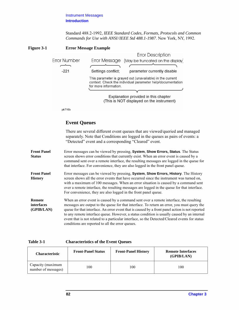
Instrument Messages
Introduction
Standard 488.2-1992, IEEE Standard Codes, Formats, Protocols and Common Commands for Use with ANSI/IEEE Std 488.1-1987. New York, NY, 1992.
Figure 3-1 Error Message Example
Event Queues
There are several different event queues that are viewed/queried and managed separately. Note that Conditions are logged in the queues as pairs of events: a “Detected” event and a corresponding “Cleared” event.
Front Panel Status
Error messages can be viewed by pressing, System, Show Errors, Status. The Status screen shows error conditions that currently exist. When an error event is caused by a command sent over a remote interface, the resulting messages are logged in the queue for that interface. For convenience, they are also logged in the front panel queue.
Front Panel History
Error messages can be viewed by pressing, System, Show Errors, History. The History screen shows all the error events that have occurred since the instrument was turned on, with a maximum of 100 messages. When an error situation is caused by a command sent over a remote interface, the resulting messages are logged in the queue for that interface. For convenience, they are also logged in the front panel queue.
Remote interfaces (GPIB/LAN)
When an error event is caused by a command sent over a remote interface, the resulting messages are output to the queue for that interface. To return an error, you must query the queue for that interface. An error event that is caused by a front panel action is not reported to any remote interface queue. However, a status condition is usually caused by an internal event that is not related to a particular interface, so the Detected/Cleared events for status conditions are reported to all the error queues.
Table 3-1 Characteristics of the Event Queues
CharacteristicFront-Panel Status Front-Panel History Remote Interfaces
(GPIB/LAN)
Capacity (maximum number of messages)
100 100 100
82 Chapter 3
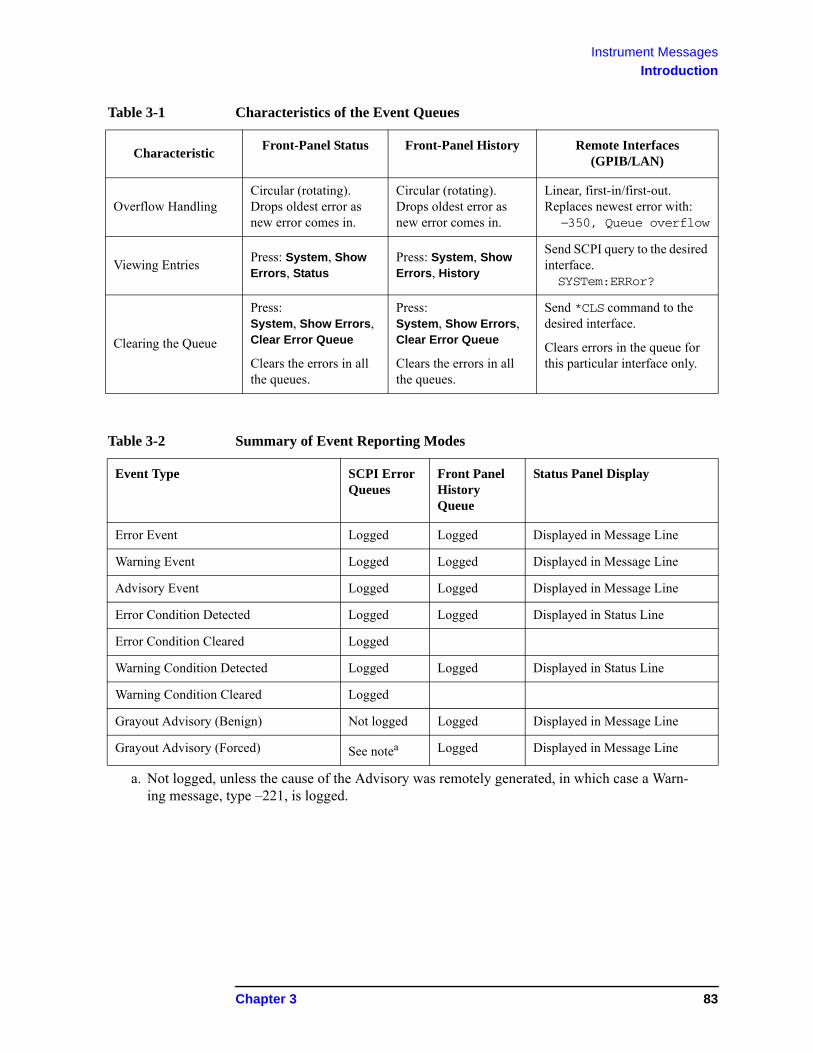
Instrument Messages
Introduction
Overflow HandlingCircular (rotating).Drops oldest error as new error comes in.
Circular (rotating).Drops oldest error as new error comes in.
Linear, first-in/first-out.Replaces newest error with:
−350, Queue overflow
Viewing EntriesPress: System, Show Errors, Status
Press: System, Show Errors, History
Send SCPI query to the desired interface.SYSTem:ERRor?
Clearing the Queue
Press: System, Show Errors, Clear Error Queue
Clears the errors in all the queues.
Press: System, Show Errors, Clear Error Queue
Clears the errors in all the queues.
Send *CLS command to the desired interface.
Clears errors in the queue for this particular interface only.
Table 3-1 Characteristics of the Event Queues
CharacteristicFront-Panel Status Front-Panel History Remote Interfaces
(GPIB/LAN)
Table 3-2 Summary of Event Reporting Modes
Event Type SCPI Error Queues
Front Panel History Queue
Status Panel Display
Error Event Logged Logged Displayed in Message Line
Warning Event Logged Logged Displayed in Message Line
Advisory Event Logged Logged Displayed in Message Line
Error Condition Detected Logged Logged Displayed in Status Line
Error Condition Cleared Logged
Warning Condition Detected Logged Logged Displayed in Status Line
Warning Condition Cleared Logged
Grayout Advisory (Benign) Not logged Logged Displayed in Message Line
Grayout Advisory (Forced) See notea Logged Displayed in Message Line
a. Not logged, unless the cause of the Advisory was remotely generated, in which case a Warn-ing message, type –221, is logged.
Chapter 3 83
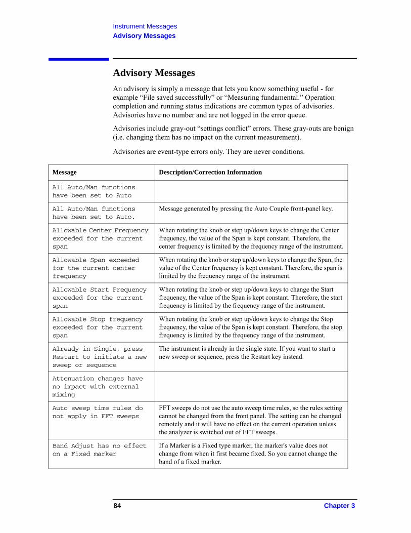
Instrument Messages
Advisory Messages
Advisory Messages
An advisory is simply a message that lets you know something useful - for example “File saved successfully” or “Measuring fundamental.” Operation completion and running status indications are common types of advisories. Advisories have no number and are not logged in the error queue.
Advisories include gray-out “settings conflict” errors. These gray-outs are benign (i.e. changing them has no impact on the current measurement).
Advisories are event-type errors only. They are never conditions.
Message Description/Correction Information
All Auto/Man functions have been set to Auto
All Auto/Man functions have been set to Auto.
Message generated by pressing the Auto Couple front-panel key.
Allowable Center Frequency exceeded for the current span
When rotating the knob or step up/down keys to change the Center frequency, the value of the Span is kept constant. Therefore, the center frequency is limited by the frequency range of the instrument.
Allowable Span exceeded for the current center frequency
When rotating the knob or step up/down keys to change the Span, the value of the Center frequency is kept constant. Therefore, the span is limited by the frequency range of the instrument.
Allowable Start Frequency exceeded for the current span
When rotating the knob or step up/down keys to change the Start frequency, the value of the Span is kept constant. Therefore, the start frequency is limited by the frequency range of the instrument.
Allowable Stop frequency exceeded for the current span
When rotating the knob or step up/down keys to change the Stop frequency, the value of the Span is kept constant. Therefore, the stop frequency is limited by the frequency range of the instrument.
Already in Single, press Restart to initiate a new sweep or sequence
The instrument is already in the single state. If you want to start a new sweep or sequence, press the Restart key instead.
Attenuation changes have no impact with external mixing
Auto sweep time rules do not apply in FFT sweeps
FFT sweeps do not use the auto sweep time rules, so the rules setting cannot be changed from the front panel. The setting can be changed remotely and it will have no effect on the current operation unless the analyzer is switched out of FFT sweeps.
Band Adjust has no effect on a Fixed marker
If a Marker is a Fixed type marker, the marker's value does not change from when it first became fixed. So you cannot change the band of a fixed marker.
84 Chapter 3
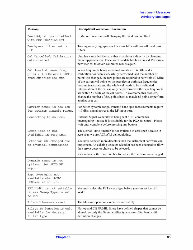
Instrument Messages
Advisory Messages
Band Adjust has no effect with Mkr Function Off
If Marker Function is off changing the band has no effect
Band-pass filter set to OFF
Turning on any high-pass or low-pass filter will turn off band pass filters.
Cal Cancelled; Calibration data cleared
User has cancelled the cal either directly or indirectly by changing the setup parameters. The current cal data has been erased. Perform a new user cal to obtain calibrated results again.
Cal Invalid: meas freq pt(s) > 3.6GHz are > 50MHz from existing Cal pts
When freq points being measured are above 3.6 GHz and a calibration has been successfully performed, and the number of points are changed, the new points are required to be within 50 MHz of the current cal points or the preselector optimize frequencies become inaccurate and the whole cal needs to be invalidated. Interpolation of the cal can only be performed if the new freq points are within 50 MHz of the cal points. To overcome this problem, change the number of freq points back to match cal points or perform another user cal.
Carrier power is too low for optimum dynamic range.
For better dynamic range, transmit band spur measurements require >10 dBm signal power at the RF input port.
Connecting to source… External Signal Generator is being sent SCPI commands interrogating it to see if it is suitable for the PXA to control. Please wait until complete before pressing any buttons.
Demod Time is not available in Zero Span
The Demod Time function is not available in zero span because in zero span we are ALWAYS demodulating.
Detector <X> changed due to physical constraints
You have selected more detectors than the instrument hardware can implement. An existing detector selection has been changed to allow the current detector choice to be selected.
<X> indicates the trace number for which the detector was changed.
Dynamic range is not optimum. Set AUTO RF input.
Exp. Averaging not available when AUTO PhNoise is active.
FFT Width is not settable unless Sweep Type is set to FFT
You must select the FFT sweep type before you can set the FFT Width
File <filename> saved The file save operation executed successfully.
Filter BW function is only available for Gaussian filter type
Flattop and CISPR/MIL filters have defined shapes that cannot be altered. So only the Gaussian filter type allows filter bandwidth definition changes.
Message Description/Correction Information
Chapter 3 85
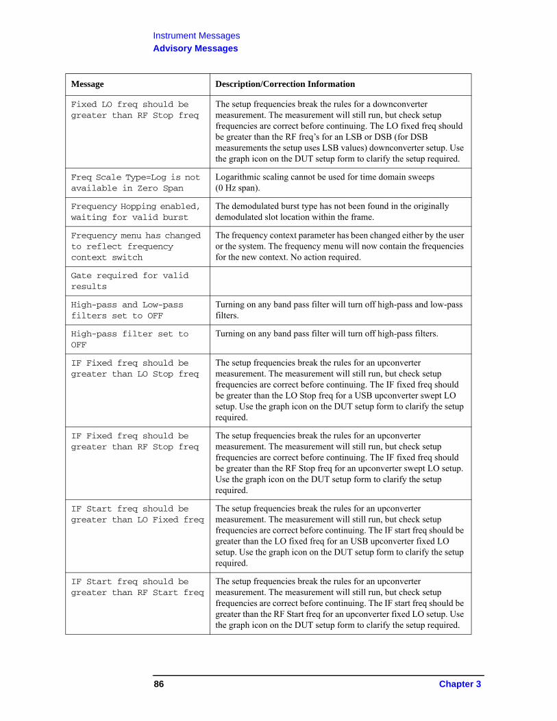
Instrument Messages
Advisory Messages
Fixed LO freq should be greater than RF Stop freq
The setup frequencies break the rules for a downconverter measurement. The measurement will still run, but check setup frequencies are correct before continuing. The LO fixed freq should be greater than the RF freq’s for an LSB or DSB (for DSB measurements the setup uses LSB values) downconverter setup. Use the graph icon on the DUT setup form to clarify the setup required.
Freq Scale Type=Log is not available in Zero Span
Logarithmic scaling cannot be used for time domain sweeps (0 Hz span).
Frequency Hopping enabled, waiting for valid burst
The demodulated burst type has not been found in the originally demodulated slot location within the frame.
Frequency menu has changed to reflect frequency context switch
The frequency context parameter has been changed either by the user or the system. The frequency menu will now contain the frequencies for the new context. No action required.
Gate required for valid results
High-pass and Low-pass filters set to OFF
Turning on any band pass filter will turn off high-pass and low-pass filters.
High-pass filter set to OFF
Turning on any band pass filter will turn off high-pass filters.
IF Fixed freq should be greater than LO Stop freq
The setup frequencies break the rules for an upconverter measurement. The measurement will still run, but check setup frequencies are correct before continuing. The IF fixed freq should be greater than the LO Stop freq for a USB upconverter swept LO setup. Use the graph icon on the DUT setup form to clarify the setup required.
IF Fixed freq should be greater than RF Stop freq
The setup frequencies break the rules for an upconverter measurement. The measurement will still run, but check setup frequencies are correct before continuing. The IF fixed freq should be greater than the RF Stop freq for an upconverter swept LO setup. Use the graph icon on the DUT setup form to clarify the setup required.
IF Start freq should be greater than LO Fixed freq
The setup frequencies break the rules for an upconverter measurement. The measurement will still run, but check setup frequencies are correct before continuing. The IF start freq should be greater than the LO fixed freq for an USB upconverter fixed LO setup. Use the graph icon on the DUT setup form to clarify the setup required.
IF Start freq should be greater than RF Start freq
The setup frequencies break the rules for an upconverter measurement. The measurement will still run, but check setup frequencies are correct before continuing. The IF start freq should be greater than the RF Start freq for an upconverter fixed LO setup. Use the graph icon on the DUT setup form to clarify the setup required.
Message Description/Correction Information
86 Chapter 3
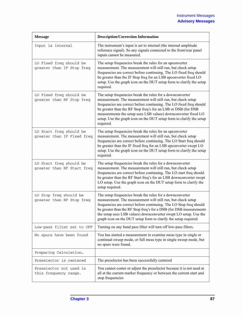
Instrument Messages
Advisory Messages
Input is internal The instrument’s input is set to internal (the internal amplitude reference signal). So any signals connected to the front/rear panel inputs cannot be measured.
LO Fixed freq should be greater than IF Stop freq
The setup frequencies break the rules for an upconverter measurement. The measurement will still run, but check setup frequencies are correct before continuing. The LO fixed freq should be greater than the IF Stop freq for an LSB upconverter fixed LO setup. Use the graph icon on the DUT setup form to clarify the setup required.
LO Fixed freq should be greater than RF Stop freq
The setup frequencies break the rules for a downconverter measurement. The measurement will still run, but check setup frequencies are correct before continuing. The LO fixed freq should be greater than the RF Stop freq’s for an LSB or DSB (for DSB measurements the setup uses LSB values) downconverter fixed LO setup. Use the graph icon on the DUT setup form to clarify the setup required.
LO Start freq should be greater than IF Fixed freq
The setup frequencies break the rules for an upconverter measurement. The measurement will still run, but check setup frequencies are correct before continuing. The LO Start freq should be greater than the IF fixed freq for an LSB upconverter swept LO setup. Use the graph icon on the DUT setup form to clarify the setup required.
LO Start freq should be greater than RF Start freq
The setup frequencies break the rules for a downconverter measurement. The measurement will still run, but check setup frequencies are correct before continuing. The LO start freq should be greater than the RF Start freq’s for an LSB downconverter swept LO setup. Use the graph icon on the DUT setup form to clarify the setup required.
LO Stop freq should be greater than RF Stop freq
The setup frequencies break the rules for a downconverter measurement. The measurement will still run, but check setup frequencies are correct before continuing. The LO Stop freq should be greater than the RF Stop freq’s for a DSB (for DSB measurements the setup uses LSB values) downconverter swept LO setup. Use the graph icon on the DUT setup form to clarify the setup required.
Low-pass filter set to OFF Turning on any band pass filter will turn off low-pass filters.
No spurs have been found You has started a measurement in examine meas type in single or continual sweep mode, or full meas type in single sweep mode, but no spurs were found.
Preparing Calculation…
Preselector is centered The preselector has been successfully centered
Preselector not used in this frequency range.
You cannot center or adjust the preselector because it is not used at all at the current marker frequency or between the current start and stop frequencies
Message Description/Correction Information
Chapter 3 87
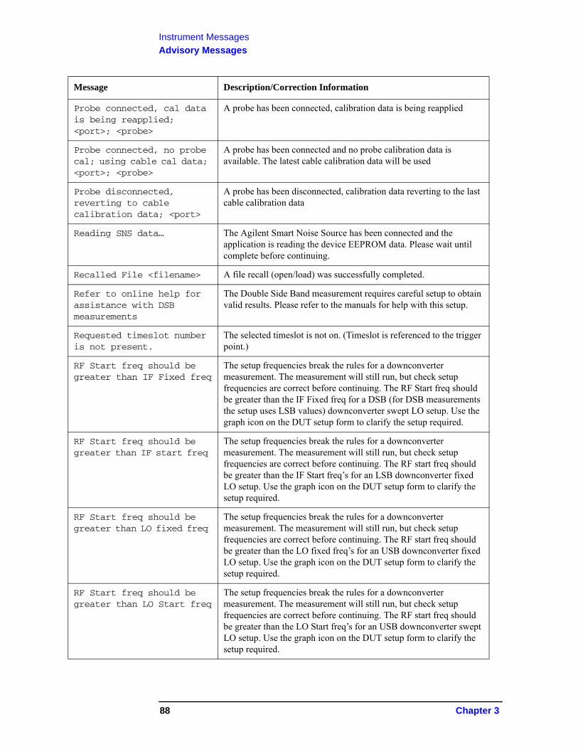
Instrument Messages
Advisory Messages
Probe connected, cal data is being reapplied; <port>; <probe>
A probe has been connected, calibration data is being reapplied
Probe connected, no probe cal; using cable cal data; <port>; <probe>
A probe has been connected and no probe calibration data is available. The latest cable calibration data will be used
Probe disconnected, reverting to cable calibration data; <port>
A probe has been disconnected, calibration data reverting to the last cable calibration data
Reading SNS data… The Agilent Smart Noise Source has been connected and the application is reading the device EEPROM data. Please wait until complete before continuing.
Recalled File <filename> A file recall (open/load) was successfully completed.
Refer to online help for assistance with DSB measurements
The Double Side Band measurement requires careful setup to obtain valid results. Please refer to the manuals for help with this setup.
Requested timeslot number is not present.
The selected timeslot is not on. (Timeslot is referenced to the trigger point.)
RF Start freq should be greater than IF Fixed freq
The setup frequencies break the rules for a downconverter measurement. The measurement will still run, but check setup frequencies are correct before continuing. The RF Start freq should be greater than the IF Fixed freq for a DSB (for DSB measurements the setup uses LSB values) downconverter swept LO setup. Use the graph icon on the DUT setup form to clarify the setup required.
RF Start freq should be greater than IF start freq
The setup frequencies break the rules for a downconverter measurement. The measurement will still run, but check setup frequencies are correct before continuing. The RF start freq should be greater than the IF Start freq’s for an LSB downconverter fixed LO setup. Use the graph icon on the DUT setup form to clarify the setup required.
RF Start freq should be greater than LO fixed freq
The setup frequencies break the rules for a downconverter measurement. The measurement will still run, but check setup frequencies are correct before continuing. The RF start freq should be greater than the LO fixed freq’s for an USB downconverter fixed LO setup. Use the graph icon on the DUT setup form to clarify the setup required.
RF Start freq should be greater than LO Start freq
The setup frequencies break the rules for a downconverter measurement. The measurement will still run, but check setup frequencies are correct before continuing. The RF start freq should be greater than the LO Start freq’s for an USB downconverter swept LO setup. Use the graph icon on the DUT setup form to clarify the setup required.
Message Description/Correction Information
88 Chapter 3
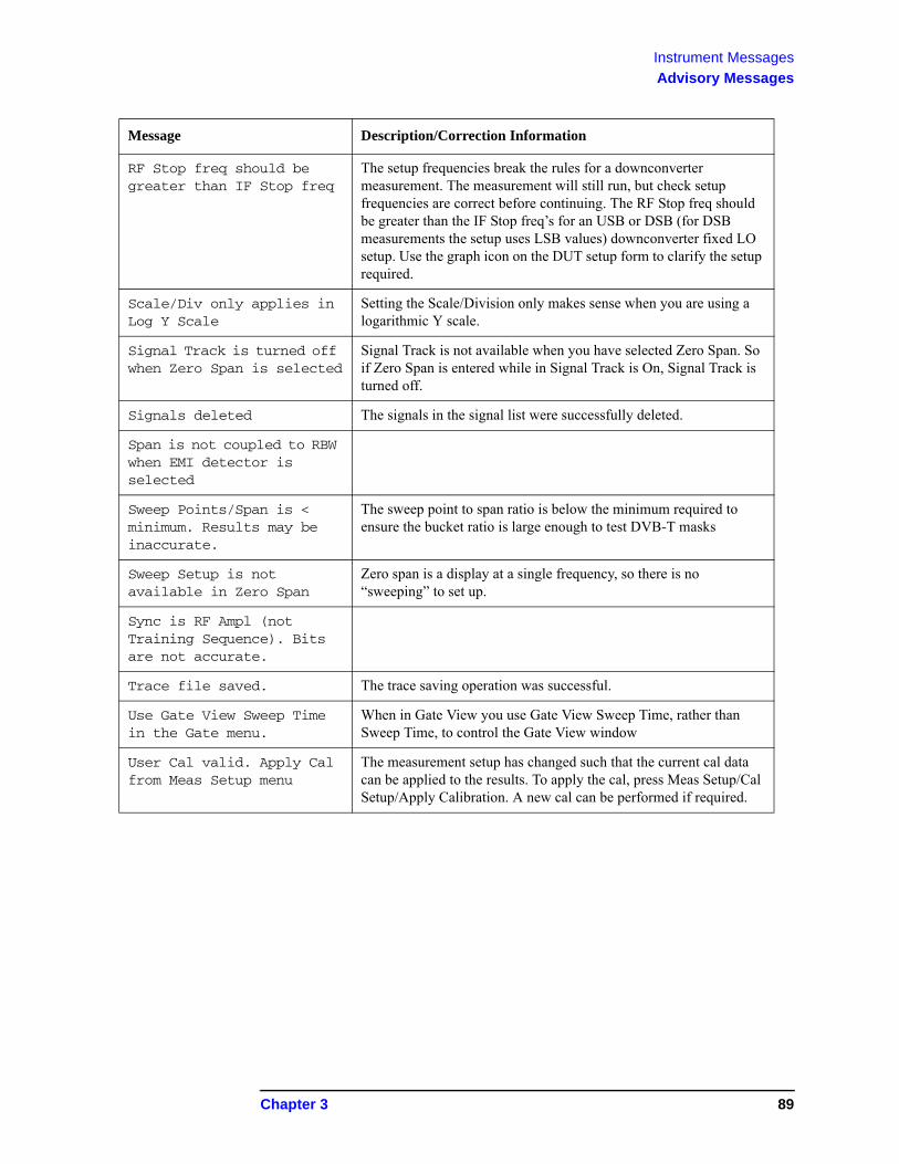
Instrument Messages
Advisory Messages
RF Stop freq should be greater than IF Stop freq
The setup frequencies break the rules for a downconverter measurement. The measurement will still run, but check setup frequencies are correct before continuing. The RF Stop freq should be greater than the IF Stop freq’s for an USB or DSB (for DSB measurements the setup uses LSB values) downconverter fixed LO setup. Use the graph icon on the DUT setup form to clarify the setup required.
Scale/Div only applies in Log Y Scale
Setting the Scale/Division only makes sense when you are using a logarithmic Y scale.
Signal Track is turned off when Zero Span is selected
Signal Track is not available when you have selected Zero Span. So if Zero Span is entered while in Signal Track is On, Signal Track is turned off.
Signals deleted The signals in the signal list were successfully deleted.
Span is not coupled to RBW when EMI detector is selected
Sweep Points/Span is < minimum. Results may be inaccurate.
The sweep point to span ratio is below the minimum required to ensure the bucket ratio is large enough to test DVB-T masks
Sweep Setup is not available in Zero Span
Zero span is a display at a single frequency, so there is no “sweeping” to set up.
Sync is RF Ampl (not Training Sequence). Bits are not accurate.
Trace file saved. The trace saving operation was successful.
Use Gate View Sweep Time in the Gate menu.
When in Gate View you use Gate View Sweep Time, rather than Sweep Time, to control the Gate View window
User Cal valid. Apply Cal from Meas Setup menu
The measurement setup has changed such that the current cal data can be applied to the results. To apply the cal, press Meas Setup/Cal Setup/Apply Calibration. A new cal can be performed if required.
Message Description/Correction Information
Chapter 3 89
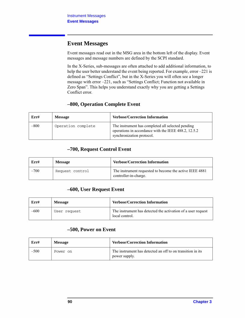
Instrument Messages
Event Messages
Event Messages
Event messages read out in the MSG area in the bottom left of the display. Event messages and message numbers are defined by the SCPI standard.
In the X-Series, sub-messages are often attached to add additional information, to help the user better understand the event being reported. For example, error –221 is defined as “Settings Conflict”, but in the X-Series you will often see a longer message with error –221, such as “Settings Conflict; Function not available in Zero Span”. This helps you understand exactly why you are getting a Settings Conflict error.
–800, Operation Complete Event
–700, Request Control Event
–600, User Request Event
–500, Power on Event
Err# Message Verbose/Correction Information
–800 Operation complete The instrument has completed all selected pending operations in accordance with the IEEE 488.2, 12.5.2 synchronization protocol.
Err# Message Verbose/Correction Information
–700 Request control The instrument requested to become the active IEEE 4881 controller-in-charge.
Err# Message Verbose/Correction Information
–600 User request The instrument has detected the activation of a user request local control.
Err# Message Verbose/Correction Information
–500 Power on The instrument has detected an off to on transition in its power supply.
90 Chapter 3
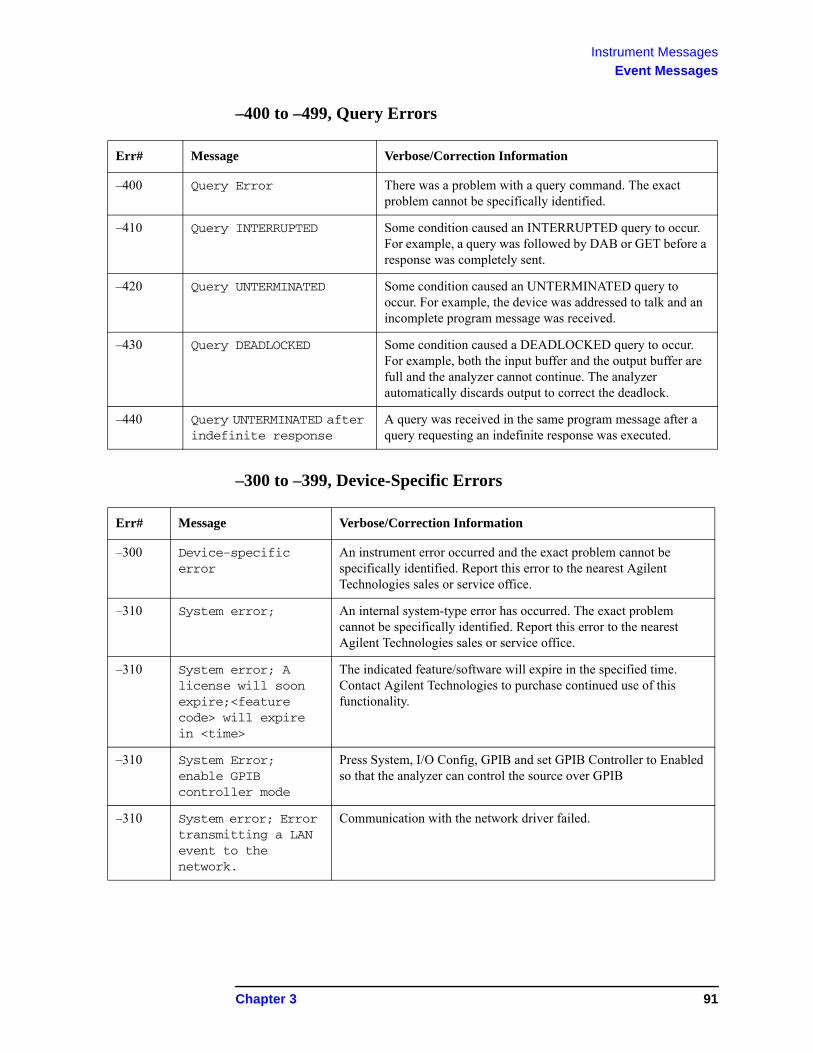
Instrument Messages
Event Messages
–400 to –499, Query Errors
–300 to –399, Device-Specific Errors
Err# Message Verbose/Correction Information
–400 Query Error There was a problem with a query command. The exact problem cannot be specifically identified.
–410 Query INTERRUPTED Some condition caused an INTERRUPTED query to occur. For example, a query was followed by DAB or GET before a response was completely sent.
–420 Query UNTERMINATED Some condition caused an UNTERMINATED query to occur. For example, the device was addressed to talk and an incomplete program message was received.
–430 Query DEADLOCKED Some condition caused a DEADLOCKED query to occur. For example, both the input buffer and the output buffer are full and the analyzer cannot continue. The analyzer automatically discards output to correct the deadlock.
–440 Query UNTERMINATED after indefinite response
A query was received in the same program message after a query requesting an indefinite response was executed.
Err# Message Verbose/Correction Information
–300 Device-specific error
An instrument error occurred and the exact problem cannot be specifically identified. Report this error to the nearest Agilent Technologies sales or service office.
–310 System error; An internal system-type error has occurred. The exact problem cannot be specifically identified. Report this error to the nearest Agilent Technologies sales or service office.
–310 System error; A license will soon expire;<feature code> will expire in <time>
The indicated feature/software will expire in the specified time. Contact Agilent Technologies to purchase continued use of this functionality.
–310 System Error; enable GPIB controller mode
Press System, I/O Config, GPIB and set GPIB Controller to Enabled so that the analyzer can control the source over GPIB
–310 System error; Error transmitting a LAN event to the network.
Communication with the network driver failed.
Chapter 3 91
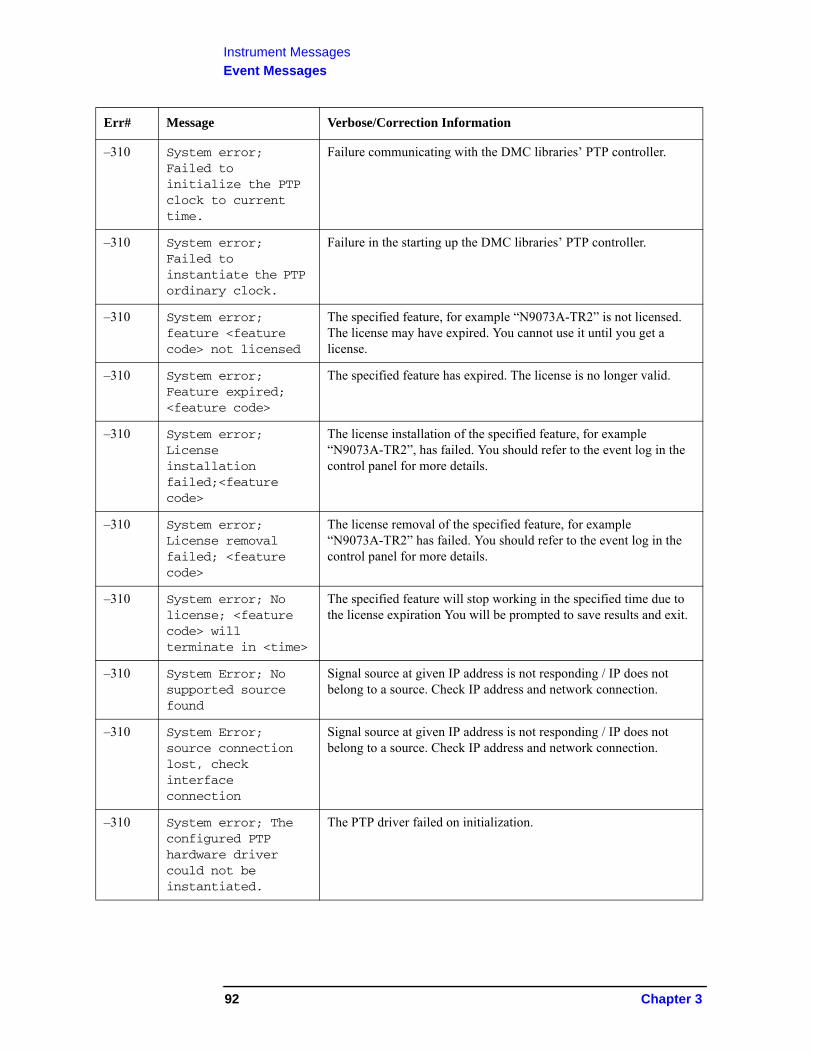
Instrument Messages
Event Messages
–310 System error; Failed to initialize the PTP clock to current time.
Failure communicating with the DMC libraries’ PTP controller.
–310 System error; Failed to instantiate the PTP ordinary clock.
Failure in the starting up the DMC libraries’ PTP controller.
–310 System error; feature <feature code> not licensed
The specified feature, for example “N9073A-TR2” is not licensed. The license may have expired. You cannot use it until you get a license.
–310 System error; Feature expired; <feature code>
The specified feature has expired. The license is no longer valid.
–310 System error; License installation failed;<feature code>
The license installation of the specified feature, for example “N9073A-TR2”, has failed. You should refer to the event log in the control panel for more details.
–310 System error; License removal failed; <feature code>
The license removal of the specified feature, for example “N9073A-TR2” has failed. You should refer to the event log in the control panel for more details.
–310 System error; No license; <feature code> will terminate in <time>
The specified feature will stop working in the specified time due to the license expiration You will be prompted to save results and exit.
–310 System Error; No supported source found
Signal source at given IP address is not responding / IP does not belong to a source. Check IP address and network connection.
–310 System Error; source connection lost, check interface connection
Signal source at given IP address is not responding / IP does not belong to a source. Check IP address and network connection.
–310 System error; The configured PTP hardware driver could not be instantiated.
The PTP driver failed on initialization.
Err# Message Verbose/Correction Information
92 Chapter 3
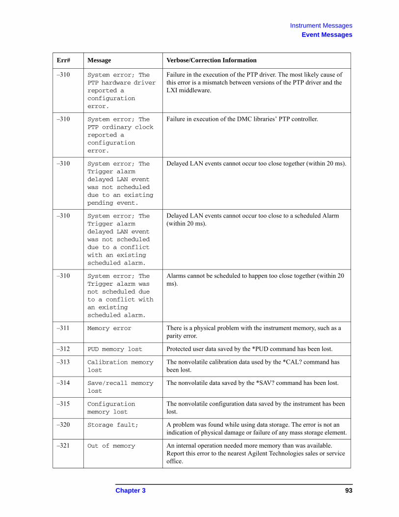
Instrument Messages
Event Messages
–310 System error; The PTP hardware driver reported a configuration error.
Failure in the execution of the PTP driver. The most likely cause of this error is a mismatch between versions of the PTP driver and the LXI middleware.
–310 System error; The PTP ordinary clock reported a configuration error.
Failure in execution of the DMC libraries’ PTP controller.
–310 System error; The Trigger alarm delayed LAN event was not scheduled due to an existing pending event.
Delayed LAN events cannot occur too close together (within 20 ms).
–310 System error; The Trigger alarm delayed LAN event was not scheduled due to a conflict with an existing scheduled alarm.
Delayed LAN events cannot occur too close to a scheduled Alarm (within 20 ms).
–310 System error; The Trigger alarm was not scheduled due to a conflict with an existing scheduled alarm.
Alarms cannot be scheduled to happen too close together (within 20 ms).
–311 Memory error There is a physical problem with the instrument memory, such as a parity error.
–312 PUD memory lost Protected user data saved by the *PUD command has been lost.
–313 Calibration memory lost
The nonvolatile calibration data used by the *CAL? command has been lost.
–314 Save/recall memory lost
The nonvolatile data saved by the *SAV? command has been lost.
–315 Configuration memory lost
The nonvolatile configuration data saved by the instrument has been lost.
–320 Storage fault; A problem was found while using data storage. The error is not an indication of physical damage or failure of any mass storage element.
–321 Out of memory An internal operation needed more memory than was available. Report this error to the nearest Agilent Technologies sales or service office.
Err# Message Verbose/Correction Information
Chapter 3 93
Instrument Messages
Event Messages
–330 Self-test failed A self-test failure occurred. Report this error to the nearest Agilent Technologies sales or service office.
–340 Calibration failed The instrument requires an Align All Now. Restore the alignment by pressing System, Alignments, Align All Now.
–340 Calibration failed; <failure msg> <port>
The calibration for one of the I-Q ports did not succeed. The information in the “failure msg” field can be used to troubleshoot this problem. Contact Agilent technical support if necessary.
–350 Queue overflow An error occurred that did not get put in the error queue because the queue was full.
–360 Communication error There was a problem with instrument remote communications. The exact problem cannot be specifically identified.
–360 Communication error; SNS data read failure. Disconnect then reconnect SNS
The Agilent Smart Noise Source connected to the PXA has failed to be read by the application. Please disconnect and reconnect the SNS. If this continues to fail, then the SNS may have had its EEPROM corrupted or another hardware fault exists. Check SNS on another instrument, NFA and ESA are also SNS compatible instruments. Check the device is not an Agilent power sensor which uses the same cable interface.
–361 Parity error in program message
A parity bit was not correct when the data was received. For example, on a parallel port.
–362 Framing error in program message
A stop bit was not detected when data was received. For example, on a remote bus port.
–363 Input buffer overrun
A software or hardware input buffer on a port overflowed with data because of improper or nonexistent pacing.
–365 Time out error There was a time-out problem in the instrument. The exact problem cannot be specifically identified.
Err# Message Verbose/Correction Information
94 Chapter 3
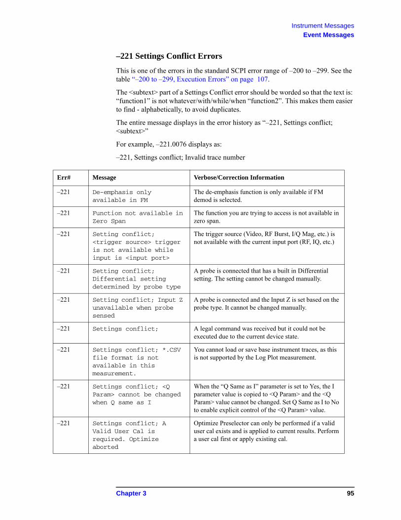
Instrument Messages
Event Messages
–221 Settings Conflict Errors
This is one of the errors in the standard SCPI error range of –200 to –299. See the table “–200 to –299, Execution Errors” on page 107.
The <subtext> part of a Settings Conflict error should be worded so that the text is: “function1” is not whatever/with/while/when “function2”. This makes them easier to find - alphabetically, to avoid duplicates.
The entire message displays in the error history as “–221, Settings conflict; <subtext>”
For example, –221.0076 displays as:
–221, Settings conflict; Invalid trace number
Err# Message Verbose/Correction Information
–221 De-emphasis only available in FM
The de-emphasis function is only available if FM demod is selected.
–221 Function not available in Zero Span
The function you are trying to access is not available in zero span.
–221 Setting conflict; <trigger source> trigger is not available while input is <input port>
The trigger source (Video, RF Burst, I/Q Mag, etc.) is not available with the current input port (RF, IQ, etc.)
–221 Setting conflict; Differential setting determined by probe type
A probe is connected that has a built in Differential setting. The setting cannot be changed manually.
–221 Setting conflict; Input Z unavailable when probe sensed
A probe is connected and the Input Z is set based on the probe type. It cannot be changed manually.
–221 Settings conflict; A legal command was received but it could not be executed due to the current device state.
–221 Settings conflict; *.CSV file format is not available in this measurement.
You cannot load or save base instrument traces, as this is not supported by the Log Plot measurement.
–221 Settings conflict; <Q Param> cannot be changed when Q same as I
When the “Q Same as I” parameter is set to Yes, the I parameter value is copied to <Q Param> and the <Q Param> value cannot be changed. Set Q Same as I to No to enable explicit control of the <Q Param> value.
–221 Settings conflict; A Valid User Cal is required. Optimize aborted
Optimize Preselector can only be performed if a valid user cal exists and is applied to current results. Perform a user cal first or apply existing cal.
Chapter 3 95
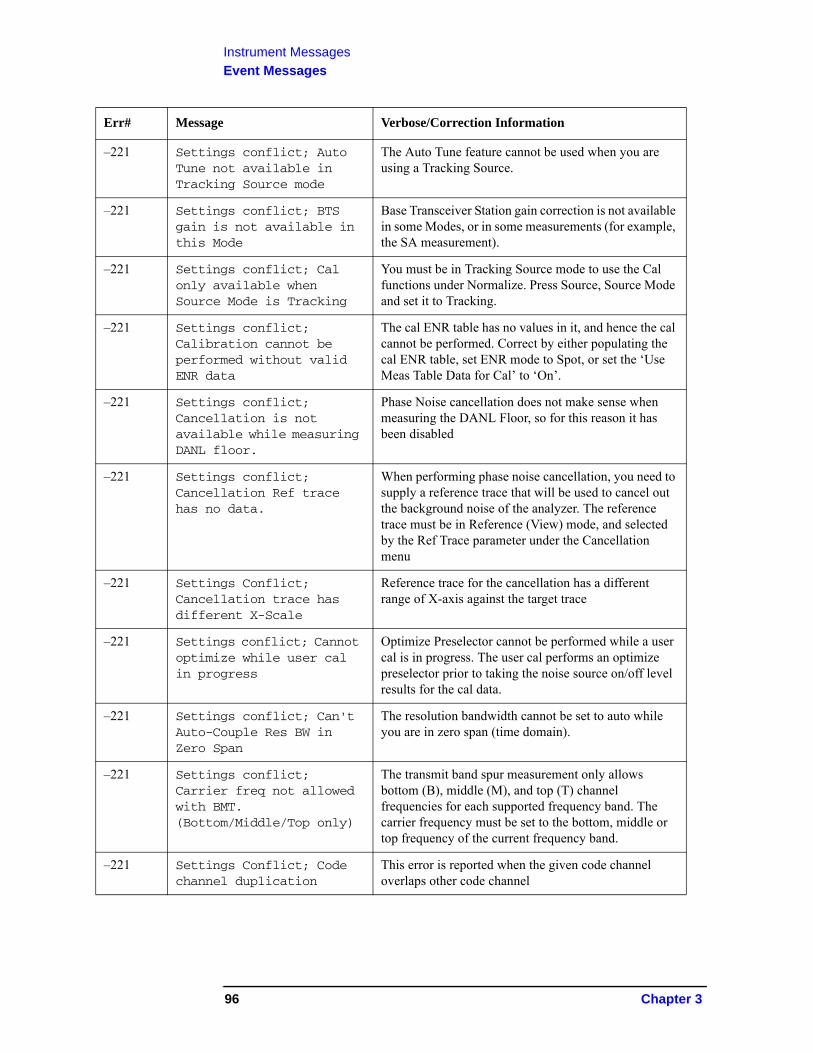
Instrument Messages
Event Messages
–221 Settings conflict; Auto Tune not available in Tracking Source mode
The Auto Tune feature cannot be used when you are using a Tracking Source.
–221 Settings conflict; BTS gain is not available in this Mode
Base Transceiver Station gain correction is not available in some Modes, or in some measurements (for example, the SA measurement).
–221 Settings conflict; Cal only available when Source Mode is Tracking
You must be in Tracking Source mode to use the Cal functions under Normalize. Press Source, Source Mode and set it to Tracking.
–221 Settings conflict; Calibration cannot be performed without valid ENR data
The cal ENR table has no values in it, and hence the cal cannot be performed. Correct by either populating the cal ENR table, set ENR mode to Spot, or set the ‘Use Meas Table Data for Cal’ to ‘On’.
–221 Settings conflict; Cancellation is not available while measuring DANL floor.
Phase Noise cancellation does not make sense when measuring the DANL Floor, so for this reason it has been disabled
–221 Settings conflict; Cancellation Ref trace has no data.
When performing phase noise cancellation, you need to supply a reference trace that will be used to cancel out the background noise of the analyzer. The reference trace must be in Reference (View) mode, and selected by the Ref Trace parameter under the Cancellation menu
–221 Settings Conflict; Cancellation trace has different X-Scale
Reference trace for the cancellation has a different range of X-axis against the target trace
–221 Settings conflict; Cannot optimize while user cal in progress
Optimize Preselector cannot be performed while a user cal is in progress. The user cal performs an optimize preselector prior to taking the noise source on/off level results for the cal data.
–221 Settings conflict; Can't Auto-Couple Res BW in Zero Span
The resolution bandwidth cannot be set to auto while you are in zero span (time domain).
–221 Settings conflict; Carrier freq not allowed with BMT. (Bottom/Middle/Top only)
The transmit band spur measurement only allows bottom (B), middle (M), and top (T) channel frequencies for each supported frequency band. The carrier frequency must be set to the bottom, middle or top frequency of the current frequency band.
–221 Settings Conflict; Code channel duplication
This error is reported when the given code channel overlaps other code channel
Err# Message Verbose/Correction Information
96 Chapter 3
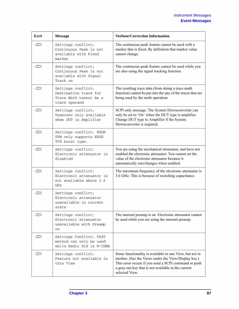
Instrument Messages
Event Messages
–221 Settings conflict; Continuous Peak is not available with Fixed marker
The continuous peak feature cannot be used with a marker that is fixed. By definition that marker value cannot change.
–221 Settings conflict; Continuous Peak is not available with Signal Track on
The continuous peak feature cannot be used while you are also using the signal tracking function.
–221 Settings conflict; Destination trace for Trace Math cannot be a trace operand
The resulting trace data (from doing a trace math function) cannot be put into the any of the traces that are being used by the math operation.
–221 Settings conflict; Downconv only available when DUT is Amplifier
SCPI only message. The System Downconverter can only be set to ‘On’ when the DUT type is amplifier. Change DUT type to Amplifier if the System Downconverter is required.
–221 Settings conflict; EDGE EVM only supports EDGE TCH burst type.
–221 Settings conflict; Electronic attenuator is disabled
You are using the mechanical attenuator, and have not enabled the electronic attenuator. You cannot set the value of the electronic attenuator because it automatically sets/changes when enabled.
–221 Settings conflict; Electronic attenuator is not available above 3.6 GHz
The maximum frequency of the electronic attenuator is 3.6 GHz. This is because of switching capacitance.
–221 Settings conflict; Electronic attenuator unavailable in current state
–221 Settings conflict; Electronic attenuator unavailable with Preamp on
The internal preamp is on. Electronic attenuator cannot be used while you are using the internal preamp.
–221 Settings Conflict; FAST method can only be used while Radio Std is W-CDMA
–221 Settings conflict; Feature not available in this View
Some functionality is available in one View, but not in another. (See the Views under the View/Display key.) This error occurs if you send a SCPI command or push a gray-out key that is not available in the current selected View.
Err# Message Verbose/Correction Information
Chapter 3 97
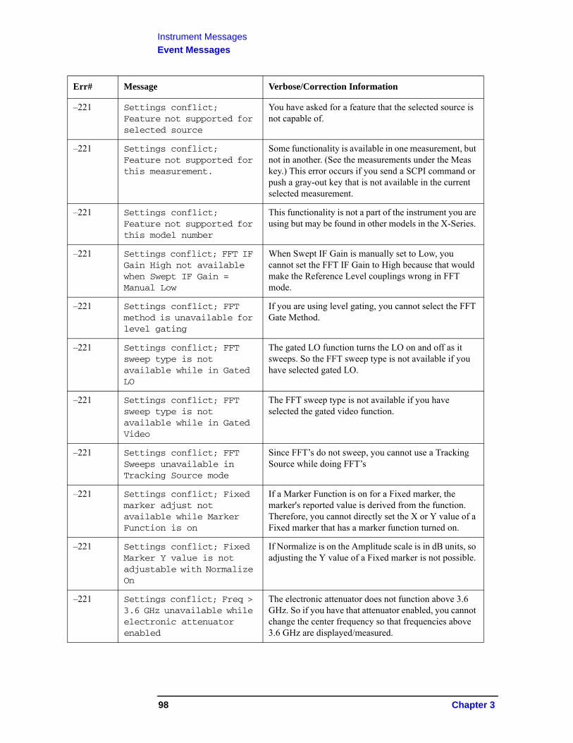
Instrument Messages
Event Messages
–221 Settings conflict; Feature not supported for selected source
You have asked for a feature that the selected source is not capable of.
–221 Settings conflict; Feature not supported for this measurement.
Some functionality is available in one measurement, but not in another. (See the measurements under the Meas key.) This error occurs if you send a SCPI command or push a gray-out key that is not available in the current selected measurement.
–221 Settings conflict; Feature not supported for this model number
This functionality is not a part of the instrument you are using but may be found in other models in the X-Series.
–221 Settings conflict; FFT IF Gain High not available when Swept IF Gain = Manual Low
When Swept IF Gain is manually set to Low, you cannot set the FFT IF Gain to High because that would make the Reference Level couplings wrong in FFT mode.
–221 Settings conflict; FFT method is unavailable for level gating
If you are using level gating, you cannot select the FFT Gate Method.
–221 Settings conflict; FFT sweep type is not available while in Gated LO
The gated LO function turns the LO on and off as it sweeps. So the FFT sweep type is not available if you have selected gated LO.
–221 Settings conflict; FFT sweep type is not available while in Gated Video
The FFT sweep type is not available if you have selected the gated video function.
–221 Settings conflict; FFT Sweeps unavailable in Tracking Source mode
Since FFT’s do not sweep, you cannot use a Tracking Source while doing FFT’s
–221 Settings conflict; Fixed marker adjust not available while Marker Function is on
If a Marker Function is on for a Fixed marker, the marker's reported value is derived from the function. Therefore, you cannot directly set the X or Y value of a Fixed marker that has a marker function turned on.
–221 Settings conflict; Fixed Marker Y value is not adjustable with Normalize On
If Normalize is on the Amplitude scale is in dB units, so adjusting the Y value of a Fixed marker is not possible.
–221 Settings conflict; Freq > 3.6 GHz unavailable while electronic attenuator enabled
The electronic attenuator does not function above 3.6 GHz. So if you have that attenuator enabled, you cannot change the center frequency so that frequencies above 3.6 GHz are displayed/measured.
Err# Message Verbose/Correction Information
98 Chapter 3
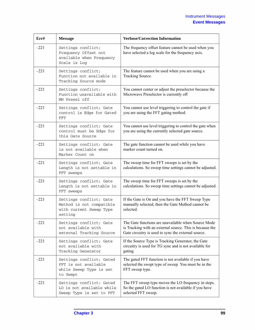
Instrument Messages
Event Messages
–221 Settings conflict; Frequency Offset not available when Frequency Scale is Log
The frequency offset feature cannot be used when you have selected a log scale for the frequency axis.
–221 Settings conflict; Function not available in Tracking Source mode
The feature cannot be used when you are using a Tracking Source.
–221 Settings conflict; Function unavailable with MW Presel off
You cannot center or adjust the preselector because the Microwave Preselector is currently off
–221 Settings conflict; Gate control is Edge for Gated FFT
You cannot use level triggering to control the gate if you are using the FFT gating method.
–221 Settings conflict; Gate control must be Edge for this Gate Source
You cannot use level triggering to control the gate when you are using the currently selected gate source.
–221 Settings conflict; Gate is not available when Marker Count on
The gate function cannot be used while you have marker count turned on.
–221 Settings conflict; Gate Length is not settable in FFT sweeps
The sweep time for FFT sweeps is set by the calculations. So sweep time settings cannot be adjusted.
–221 Settings conflict; Gate Length is not settable in FFT sweeps
The sweep time for FFT sweeps is set by the calculations. So sweep time settings cannot be adjusted.
–221 Settings conflict; Gate Method is not compatible with current Sweep Type setting
If the Gate is On and you have the FFT Sweep Type manually selected, then the Gate Method cannot be selected.
–221 Settings conflict; Gate not available with external Tracking Source
The Gate functions are unavailable when Source Mode is Tracking with an external source. This is because the Gate circuitry is used to sync the external source.
–221 Settings conflict; Gate not available with Tracking Generator
If the Source Type is Tracking Generator, the Gate circuitry is used for TG sync and is not available for gating
–221 Settings conflict; Gated FFT is not available while Sweep Type is set to Swept
The gated FFT function is not available if you have selected the swept type of sweep. You must be in the FFT sweep type.
–221 Settings conflict; Gated LO is not available while Sweep Type is set to FFT
The FFT sweep type moves the LO frequency in steps. So the gated LO function is not available if you have selected FFT sweep.
Err# Message Verbose/Correction Information
Chapter 3 99
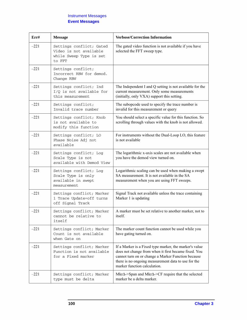
Instrument Messages
Event Messages
–221 Settings conflict; Gated Video is not available while Sweep Type is set to FFT
The gated video function is not available if you have selected the FFT sweep type.
–221 Settings conflict; Incorrect RBW for demod. Change RBW
–221 Settings conflict; Ind I/Q is not available for this measurement
The Independent I and Q setting is not available for the current measurement. Only some measurements (initially, only VXA) support this setting.
–221 Settings conflict; Invalid trace number
The subopcode used to specify the trace number is invalid for this measurement or query
–221 Settings conflict; Knob is not available to modify this function
You should select a specific value for this function. So scrolling through values with the knob is not allowed.
–221 Settings conflict; LO Phase Noise Adj not available
For instruments without the Dual-Loop LO, this feature is not available
–221 Settings conflict; Log Scale Type is not available with Demod View
The logarithmic x-axis scales are not available when you have the demod view turned on.
–221 Settings conflict; Log Scale Type is only available in swept measurement
Logarithmic scaling can be used when making a swept SA measurement. It is not available in the SA measurement when you are using FFT sweeps.
–221 Settings conflict; Marker 1 Trace Update=off turns off Signal Track
Signal Track not available unless the trace containing Marker 1 is updating
–221 Settings conflict; Marker cannot be relative to itself
A marker must be set relative to another marker, not to itself.
–221 Settings conflict; Marker Count is not available when Gate on
The marker count function cannot be used while you have gating turned on.
–221 Settings conflict; Marker Function is not available for a Fixed marker
If a Marker is a Fixed type marker, the marker's value does not change from when it first became fixed. You cannot turn on or change a Marker Function because there is no ongoing measurement data to use for the marker function calculation.
–221 Settings conflict; Marker type must be delta
MkrΔ->Span and MkrΔ->CF require that the selected marker be a delta marker.
Err# Message Verbose/Correction Information
100 Chapter 3
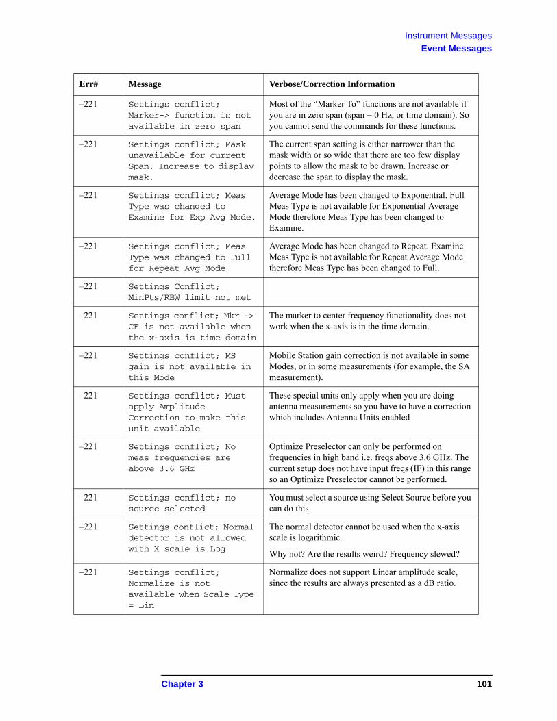
Instrument Messages
Event Messages
–221 Settings conflict; Marker-> function is not available in zero span
Most of the “Marker To” functions are not available if you are in zero span (span = 0 Hz, or time domain). So you cannot send the commands for these functions.
–221 Settings conflict; Mask unavailable for current Span. Increase to display mask.
The current span setting is either narrower than the mask width or so wide that there are too few display points to allow the mask to be drawn. Increase or decrease the span to display the mask.
–221 Settings conflict; Meas Type was changed to Examine for Exp Avg Mode.
Average Mode has been changed to Exponential. Full Meas Type is not available for Exponential Average Mode therefore Meas Type has been changed to Examine.
–221 Settings conflict; Meas Type was changed to Full for Repeat Avg Mode
Average Mode has been changed to Repeat. Examine Meas Type is not available for Repeat Average Mode therefore Meas Type has been changed to Full.
–221 Settings Conflict; MinPts/RBW limit not met
–221 Settings conflict; Mkr -> CF is not available when the x-axis is time domain
The marker to center frequency functionality does not work when the x-axis is in the time domain.
–221 Settings conflict; MS gain is not available in this Mode
Mobile Station gain correction is not available in some Modes, or in some measurements (for example, the SA measurement).
–221 Settings conflict; Must apply Amplitude Correction to make this unit available
These special units only apply when you are doing antenna measurements so you have to have a correction which includes Antenna Units enabled
–221 Settings conflict; No meas frequencies are above 3.6 GHz
Optimize Preselector can only be performed on frequencies in high band i.e. freqs above 3.6 GHz. The current setup does not have input freqs (IF) in this range so an Optimize Preselector cannot be performed.
–221 Settings conflict; no source selected
You must select a source using Select Source before you can do this
–221 Settings conflict; Normal detector is not allowed with X scale is Log
The normal detector cannot be used when the x-axis scale is logarithmic.
Why not? Are the results weird? Frequency slewed?
–221 Settings conflict; Normalize is not available when Scale Type = Lin
Normalize does not support Linear amplitude scale, since the results are always presented as a dB ratio.
Err# Message Verbose/Correction Information
Chapter 3 101
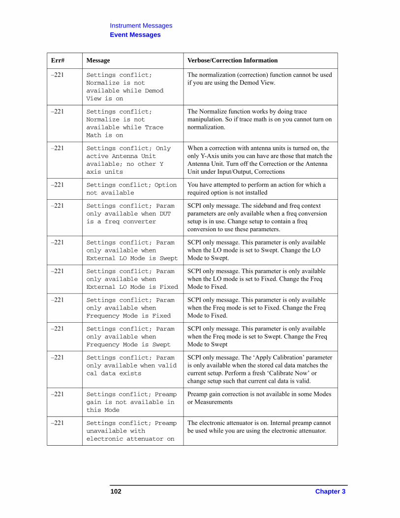
Instrument Messages
Event Messages
–221 Settings conflict; Normalize is not available while Demod View is on
The normalization (correction) function cannot be used if you are using the Demod View.
–221 Settings conflict; Normalize is not available while Trace Math is on
The Normalize function works by doing trace manipulation. So if trace math is on you cannot turn on normalization.
–221 Settings conflict; Only active Antenna Unit available; no other Y axis units
When a correction with antenna units is turned on, the only Y-Axis units you can have are those that match the Antenna Unit. Turn off the Correction or the Antenna Unit under Input/Output, Corrections
–221 Settings conflict; Option not available
You have attempted to perform an action for which a required option is not installed
–221 Settings conflict; Param only available when DUT is a freq converter
SCPI only message. The sideband and freq context parameters are only available when a freq conversion setup is in use. Change setup to contain a freq conversion to use these parameters.
–221 Settings conflict; Param only available when External LO Mode is Swept
SCPI only message. This parameter is only available when the LO mode is set to Swept. Change the LO Mode to Swept.
–221 Settings conflict; Param only available when External LO Mode is Fixed
SCPI only message. This parameter is only available when the LO mode is set to Fixed. Change the Freq Mode to Fixed.
–221 Settings conflict; Param only available when Frequency Mode is Fixed
SCPI only message. This parameter is only available when the Freq mode is set to Fixed. Change the Freq Mode to Fixed.
–221 Settings conflict; Param only available when Frequency Mode is Swept
SCPI only message. This parameter is only available when the Freq mode is set to Swept. Change the Freq Mode to Swept
–221 Settings conflict; Param only available when valid cal data exists
SCPI only message. The ‘Apply Calibration’ parameter is only available when the stored cal data matches the current setup. Perform a fresh ‘Calibrate Now’ or change setup such that current cal data is valid.
–221 Settings conflict; Preamp gain is not available in this Mode
Preamp gain correction is not available in some Modes or Measurements
–221 Settings conflict; Preamp unavailable with electronic attenuator on
The electronic attenuator is on. Internal preamp cannot be used while you are using the electronic attenuator.
Err# Message Verbose/Correction Information
102 Chapter 3
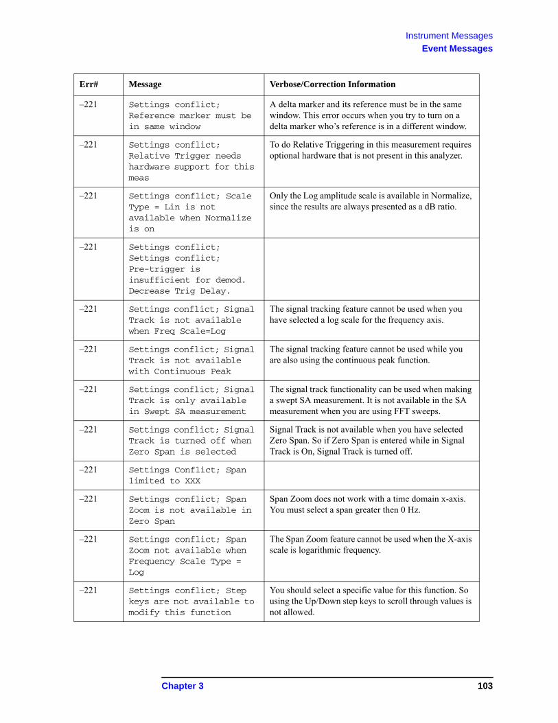
Instrument Messages
Event Messages
–221 Settings conflict; Reference marker must be in same window
A delta marker and its reference must be in the same window. This error occurs when you try to turn on a delta marker who’s reference is in a different window.
–221 Settings conflict; Relative Trigger needs hardware support for this meas
To do Relative Triggering in this measurement requires optional hardware that is not present in this analyzer.
–221 Settings conflict; Scale Type = Lin is not available when Normalize is on
Only the Log amplitude scale is available in Normalize, since the results are always presented as a dB ratio.
–221 Settings conflict; Settings conflict; Pre-trigger is insufficient for demod. Decrease Trig Delay.
–221 Settings conflict; Signal Track is not available when Freq Scale=Log
The signal tracking feature cannot be used when you have selected a log scale for the frequency axis.
–221 Settings conflict; Signal Track is not available with Continuous Peak
The signal tracking feature cannot be used while you are also using the continuous peak function.
–221 Settings conflict; Signal Track is only available in Swept SA measurement
The signal track functionality can be used when making a swept SA measurement. It is not available in the SA measurement when you are using FFT sweeps.
–221 Settings conflict; Signal Track is turned off when Zero Span is selected
Signal Track is not available when you have selected Zero Span. So if Zero Span is entered while in Signal Track is On, Signal Track is turned off.
–221 Settings Conflict; Span limited to XXX
–221 Settings conflict; Span Zoom is not available in Zero Span
Span Zoom does not work with a time domain x-axis. You must select a span greater then 0 Hz.
–221 Settings conflict; Span Zoom not available when Frequency Scale Type = Log
The Span Zoom feature cannot be used when the X-axis scale is logarithmic frequency.
–221 Settings conflict; Step keys are not available to modify this function
You should select a specific value for this function. So using the Up/Down step keys to scroll through values is not allowed.
Err# Message Verbose/Correction Information
Chapter 3 103
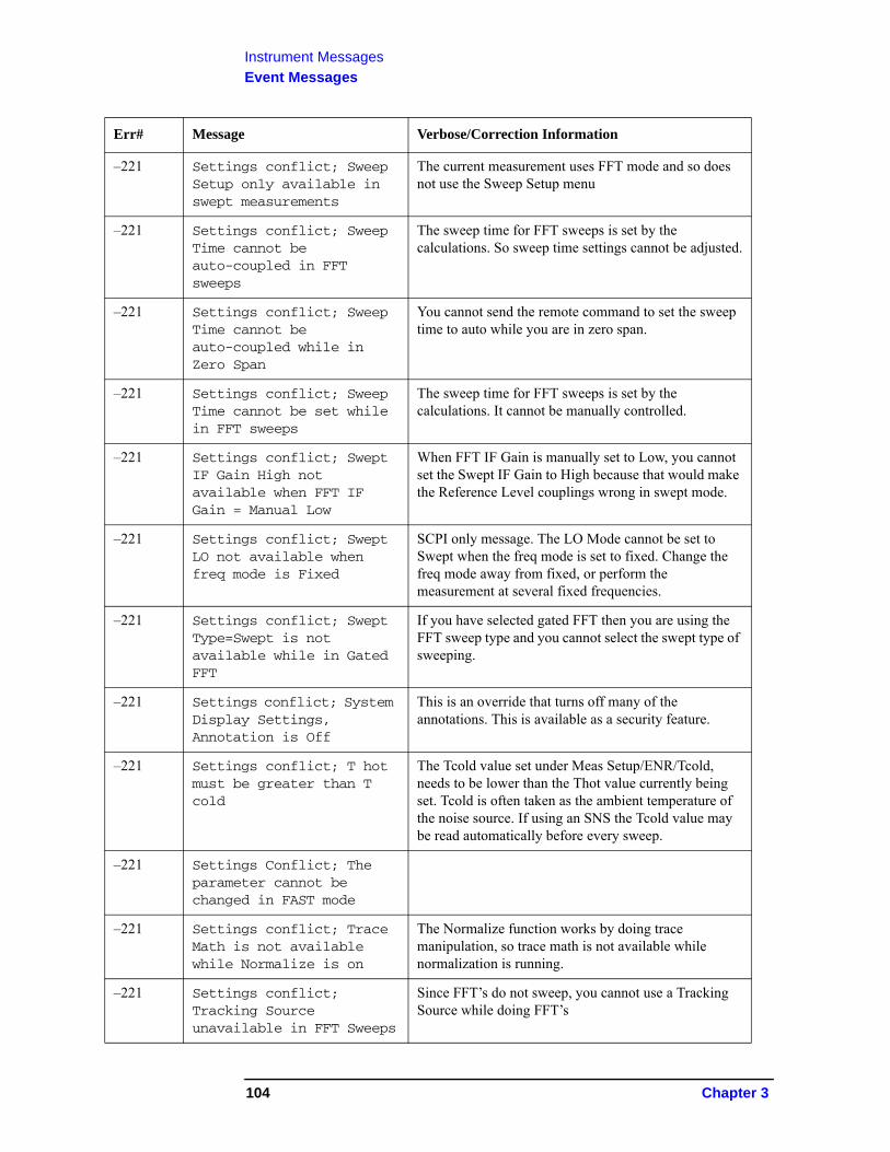
Instrument Messages
Event Messages
–221 Settings conflict; Sweep Setup only available in swept measurements
The current measurement uses FFT mode and so does not use the Sweep Setup menu
–221 Settings conflict; Sweep Time cannot be auto-coupled in FFT sweeps
The sweep time for FFT sweeps is set by the calculations. So sweep time settings cannot be adjusted.
–221 Settings conflict; Sweep Time cannot be auto-coupled while in Zero Span
You cannot send the remote command to set the sweep time to auto while you are in zero span.
–221 Settings conflict; Sweep Time cannot be set while in FFT sweeps
The sweep time for FFT sweeps is set by the calculations. It cannot be manually controlled.
–221 Settings conflict; Swept IF Gain High not available when FFT IF Gain = Manual Low
When FFT IF Gain is manually set to Low, you cannot set the Swept IF Gain to High because that would make the Reference Level couplings wrong in swept mode.
–221 Settings conflict; Swept LO not available when freq mode is Fixed
SCPI only message. The LO Mode cannot be set to Swept when the freq mode is set to fixed. Change the freq mode away from fixed, or perform the measurement at several fixed frequencies.
–221 Settings conflict; Swept Type=Swept is not available while in Gated FFT
If you have selected gated FFT then you are using the FFT sweep type and you cannot select the swept type of sweeping.
–221 Settings conflict; System Display Settings, Annotation is Off
This is an override that turns off many of the annotations. This is available as a security feature.
–221 Settings conflict; T hot must be greater than T cold
The Tcold value set under Meas Setup/ENR/Tcold, needs to be lower than the Thot value currently being set. Tcold is often taken as the ambient temperature of the noise source. If using an SNS the Tcold value may be read automatically before every sweep.
–221 Settings Conflict; The parameter cannot be changed in FAST mode
–221 Settings conflict; Trace Math is not available while Normalize is on
The Normalize function works by doing trace manipulation, so trace math is not available while normalization is running.
–221 Settings conflict; Tracking Source unavailable in FFT Sweeps
Since FFT’s do not sweep, you cannot use a Tracking Source while doing FFT’s
Err# Message Verbose/Correction Information
104 Chapter 3
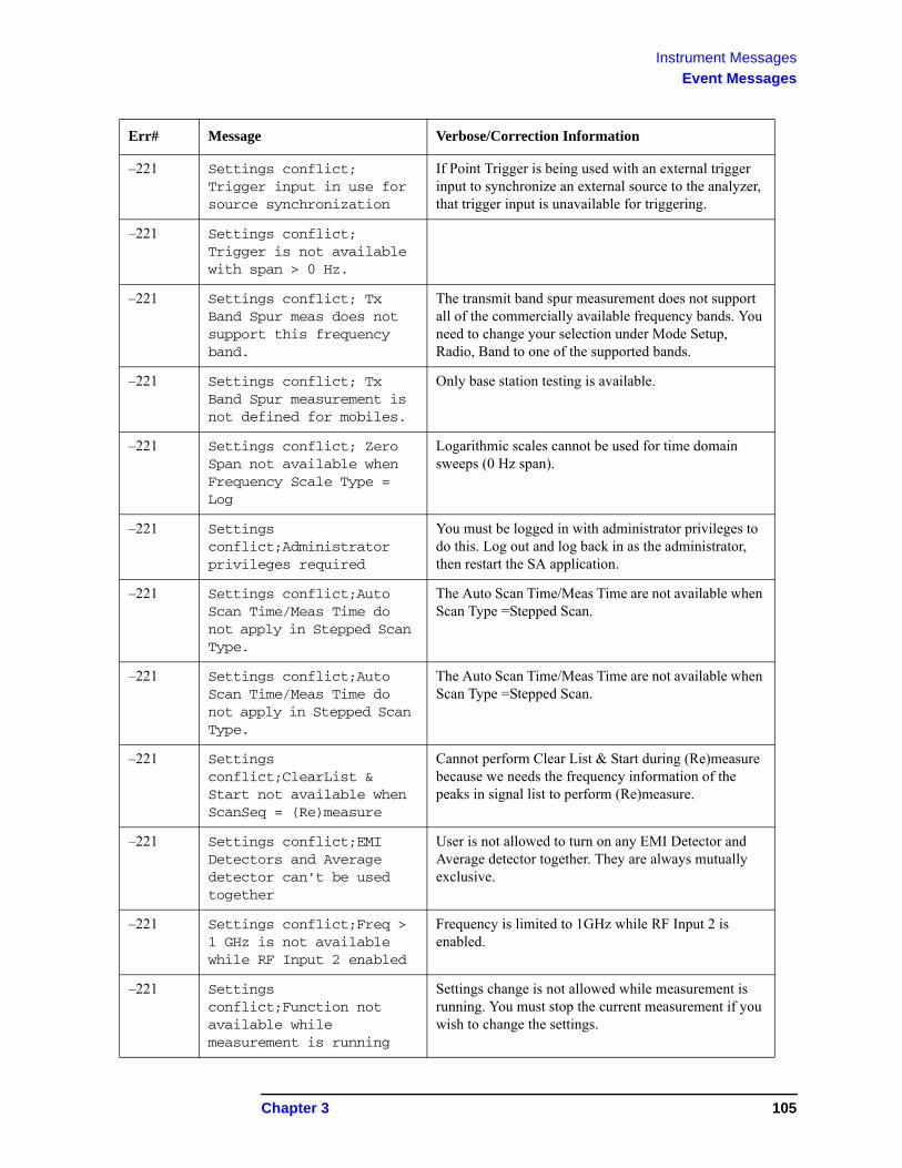
Instrument Messages
Event Messages
–221 Settings conflict; Trigger input in use for source synchronization
If Point Trigger is being used with an external trigger input to synchronize an external source to the analyzer, that trigger input is unavailable for triggering.
–221 Settings conflict; Trigger is not available with span > 0 Hz.
–221 Settings conflict; Tx Band Spur meas does not support this frequency band.
The transmit band spur measurement does not support all of the commercially available frequency bands. You need to change your selection under Mode Setup, Radio, Band to one of the supported bands.
–221 Settings conflict; Tx Band Spur measurement is not defined for mobiles.
Only base station testing is available.
–221 Settings conflict; Zero Span not available when Frequency Scale Type = Log
Logarithmic scales cannot be used for time domain sweeps (0 Hz span).
–221 Settings conflict;Administrator privileges required
You must be logged in with administrator privileges to do this. Log out and log back in as the administrator, then restart the SA application.
–221 Settings conflict;Auto Scan Time/Meas Time do not apply in Stepped Scan Type.
The Auto Scan Time/Meas Time are not available when Scan Type =Stepped Scan.
–221 Settings conflict;Auto Scan Time/Meas Time do not apply in Stepped Scan Type.
The Auto Scan Time/Meas Time are not available when Scan Type =Stepped Scan.
–221 Settings conflict;ClearList & Start not available when ScanSeq = (Re)measure
Cannot perform Clear List & Start during (Re)measure because we needs the frequency information of the peaks in signal list to perform (Re)measure.
–221 Settings conflict;EMI Detectors and Average detector can’t be used together
User is not allowed to turn on any EMI Detector and Average detector together. They are always mutually exclusive.
–221 Settings conflict;Freq > 1 GHz is not available while RF Input 2 enabled
Frequency is limited to 1GHz while RF Input 2 is enabled.
–221 Settings conflict;Function not available while measurement is running
Settings change is not allowed while measurement is running. You must stop the current measurement if you wish to change the settings.
Err# Message Verbose/Correction Information
Chapter 3 105
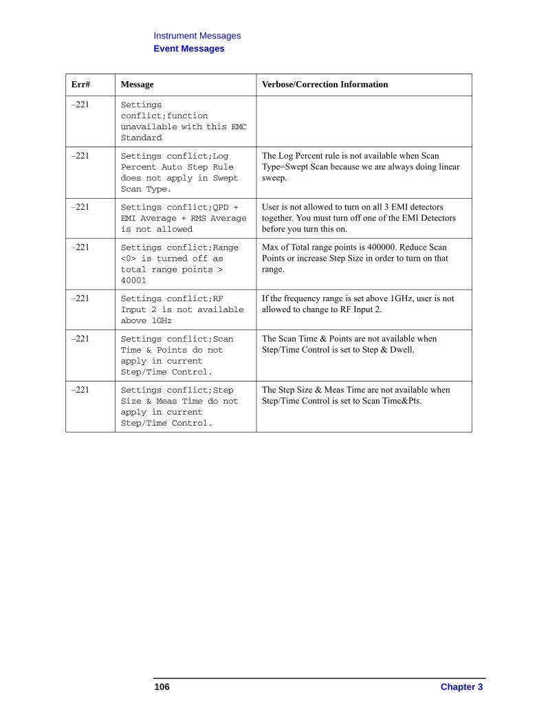
Instrument Messages
Event Messages
–221 Settings conflict;function unavailable with this EMC Standard
–221 Settings conflict;Log Percent Auto Step Rule does not apply in Swept Scan Type.
The Log Percent rule is not available when Scan Type=Swept Scan because we are always doing linear sweep.
–221 Settings conflict;QPD + EMI Average + RMS Average is not allowed
User is not allowed to turn on all 3 EMI detectors together. You must turn off one of the EMI Detectors before you turn this on.
–221 Settings conflict;Range <0> is turned off as total range points > 40001
Max of Total range points is 400000. Reduce Scan Points or increase Step Size in order to turn on that range.
–221 Settings conflict;RF Input 2 is not available above 1GHz
If the frequency range is set above 1GHz, user is not allowed to change to RF Input 2.
–221 Settings conflict;Scan Time & Points do not apply in current Step/Time Control.
The Scan Time & Points are not available when Step/Time Control is set to Step & Dwell.
–221 Settings conflict;Step Size & Meas Time do not apply in current Step/Time Control.
The Step Size & Meas Time are not available when Step/Time Control is set to Scan Time&Pts.
Err# Message Verbose/Correction Information
106 Chapter 3
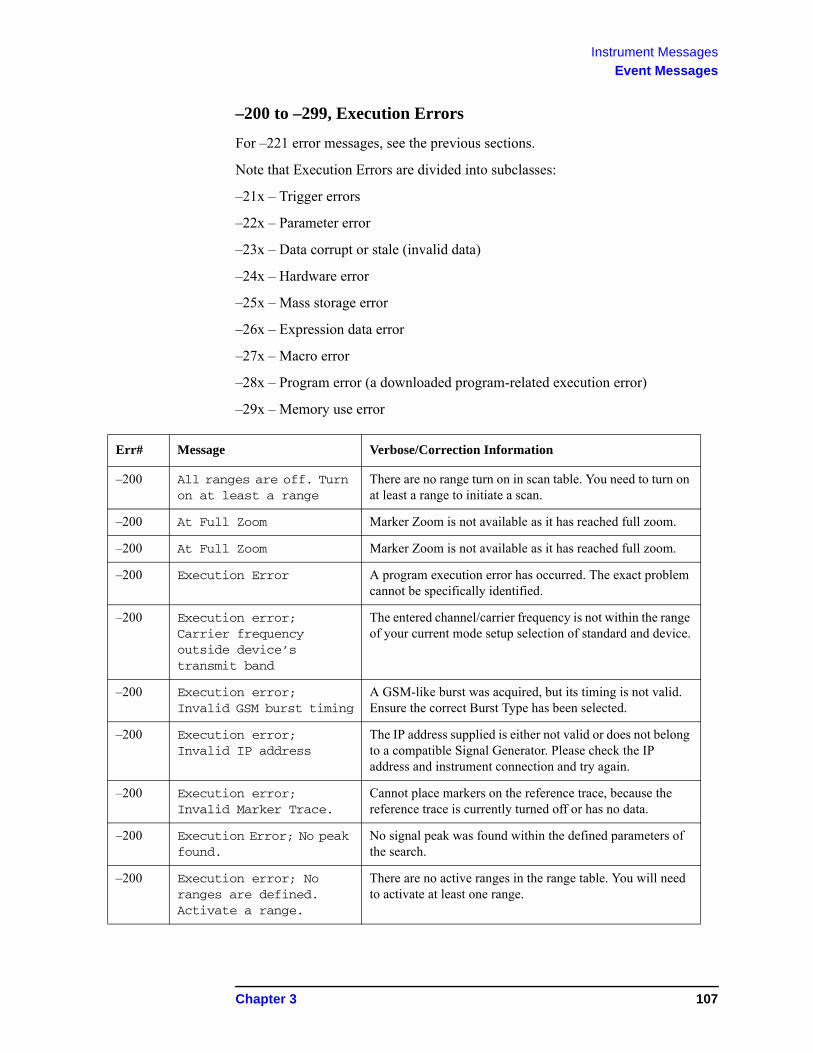
Instrument Messages
Event Messages
–200 to –299, Execution Errors
For –221 error messages, see the previous sections.
Note that Execution Errors are divided into subclasses:
–21x – Trigger errors
–22x – Parameter error
–23x – Data corrupt or stale (invalid data)
–24x – Hardware error
–25x – Mass storage error
–26x – Expression data error
–27x – Macro error
–28x – Program error (a downloaded program-related execution error)
–29x – Memory use error
Err# Message Verbose/Correction Information
–200 All ranges are off. Turn on at least a range
There are no range turn on in scan table. You need to turn on at least a range to initiate a scan.
–200 At Full Zoom Marker Zoom is not available as it has reached full zoom.
–200 At Full Zoom Marker Zoom is not available as it has reached full zoom.
–200 Execution Error A program execution error has occurred. The exact problem cannot be specifically identified.
–200 Execution error; Carrier frequency outside device’s transmit band
The entered channel/carrier frequency is not within the range of your current mode setup selection of standard and device.
–200 Execution error; Invalid GSM burst timing
A GSM-like burst was acquired, but its timing is not valid. Ensure the correct Burst Type has been selected.
–200 Execution error; Invalid IP address
The IP address supplied is either not valid or does not belong to a compatible Signal Generator. Please check the IP address and instrument connection and try again.
–200 Execution error; Invalid Marker Trace.
Cannot place markers on the reference trace, because the reference trace is currently turned off or has no data.
–200 Execution Error; No peak found.
No signal peak was found within the defined parameters of the search.
–200 Execution error; No ranges are defined. Activate a range.
There are no active ranges in the range table. You will need to activate at least one range.
Chapter 3 107
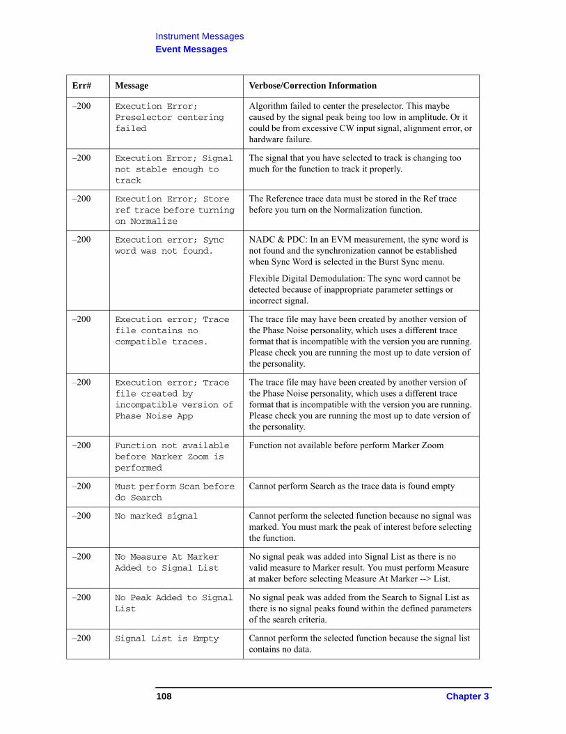
Instrument Messages
Event Messages
–200 Execution Error; Preselector centering failed
Algorithm failed to center the preselector. This maybe caused by the signal peak being too low in amplitude. Or it could be from excessive CW input signal, alignment error, or hardware failure.
–200 Execution Error; Signal not stable enough to track
The signal that you have selected to track is changing too much for the function to track it properly.
–200 Execution Error; Store ref trace before turning on Normalize
The Reference trace data must be stored in the Ref trace before you turn on the Normalization function.
–200 Execution error; Sync word was not found.
NADC & PDC: In an EVM measurement, the sync word is not found and the synchronization cannot be established when Sync Word is selected in the Burst Sync menu.
Flexible Digital Demodulation: The sync word cannot be detected because of inappropriate parameter settings or incorrect signal.
–200 Execution error; Trace file contains no compatible traces.
The trace file may have been created by another version of the Phase Noise personality, which uses a different trace format that is incompatible with the version you are running. Please check you are running the most up to date version of the personality.
–200 Execution error; Trace file created by incompatible version of Phase Noise App
The trace file may have been created by another version of the Phase Noise personality, which uses a different trace format that is incompatible with the version you are running. Please check you are running the most up to date version of the personality.
–200 Function not available before Marker Zoom is performed
Function not available before perform Marker Zoom
–200 Must perform Scan before do Search
Cannot perform Search as the trace data is found empty
–200 No marked signal Cannot perform the selected function because no signal was marked. You must mark the peak of interest before selecting the function.
–200 No Measure At Marker Added to Signal List
No signal peak was added into Signal List as there is no valid measure to Marker result. You must perform Measure at maker before selecting Measure At Marker --> List.
–200 No Peak Added to Signal List
No signal peak was added from the Search to Signal List as there is no signal peaks found within the defined parameters of the search criteria.
–200 Signal List is Empty Cannot perform the selected function because the signal list contains no data.
Err# Message Verbose/Correction Information
108 Chapter 3
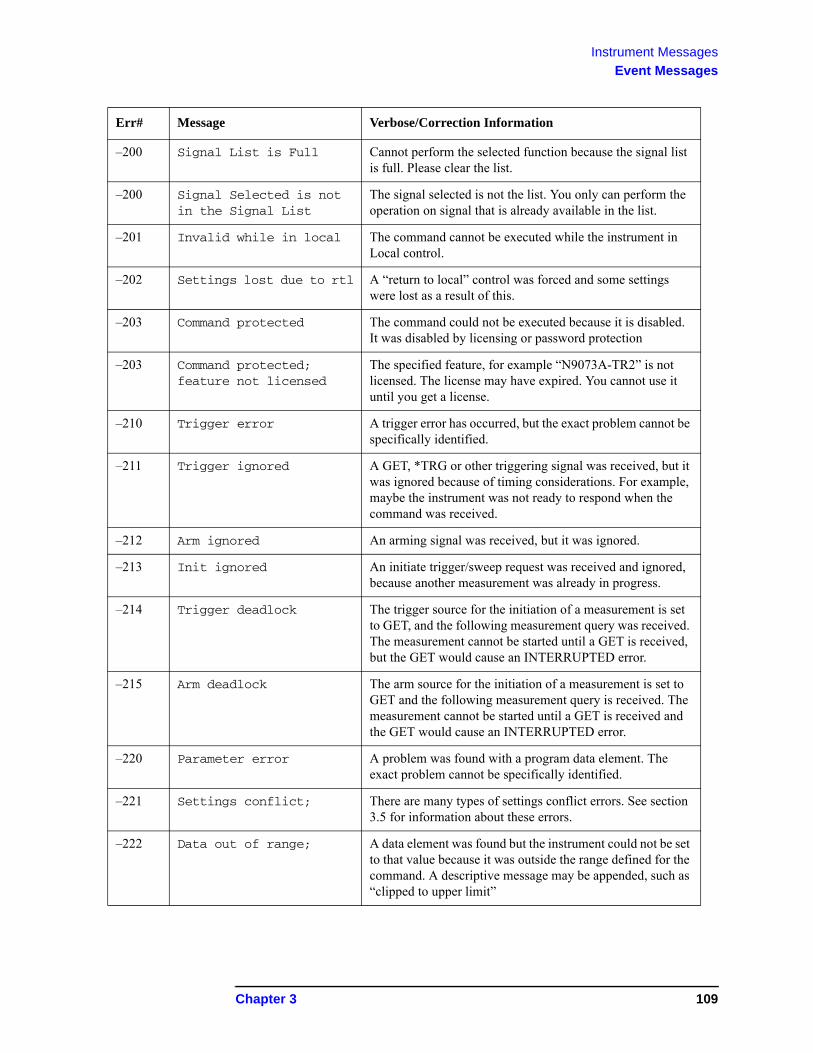
Instrument Messages
Event Messages
–200 Signal List is Full Cannot perform the selected function because the signal list is full. Please clear the list.
–200 Signal Selected is not in the Signal List
The signal selected is not the list. You only can perform the operation on signal that is already available in the list.
–201 Invalid while in local The command cannot be executed while the instrument in Local control.
–202 Settings lost due to rtl A “return to local” control was forced and some settings were lost as a result of this.
–203 Command protected The command could not be executed because it is disabled. It was disabled by licensing or password protection
–203 Command protected; feature not licensed
The specified feature, for example “N9073A-TR2” is not licensed. The license may have expired. You cannot use it until you get a license.
–210 Trigger error A trigger error has occurred, but the exact problem cannot be specifically identified.
–211 Trigger ignored A GET, *TRG or other triggering signal was received, but it was ignored because of timing considerations. For example, maybe the instrument was not ready to respond when the command was received.
–212 Arm ignored An arming signal was received, but it was ignored.
–213 Init ignored An initiate trigger/sweep request was received and ignored, because another measurement was already in progress.
–214 Trigger deadlock The trigger source for the initiation of a measurement is set to GET, and the following measurement query was received. The measurement cannot be started until a GET is received, but the GET would cause an INTERRUPTED error.
–215 Arm deadlock The arm source for the initiation of a measurement is set to GET and the following measurement query is received. The measurement cannot be started until a GET is received and the GET would cause an INTERRUPTED error.
–220 Parameter error A problem was found with a program data element. The exact problem cannot be specifically identified.
–221 Settings conflict; There are many types of settings conflict errors. See section 3.5 for information about these errors.
–222 Data out of range; A data element was found but the instrument could not be set to that value because it was outside the range defined for the command. A descriptive message may be appended, such as “clipped to upper limit”
Err# Message Verbose/Correction Information
Chapter 3 109
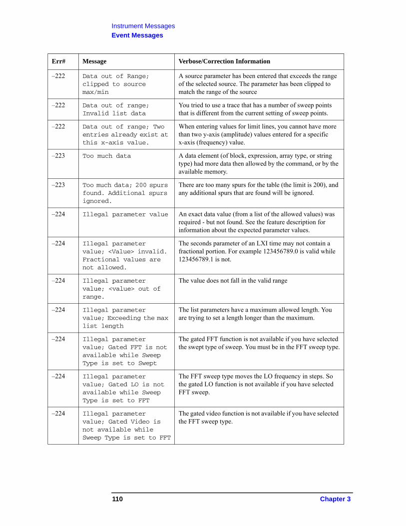
Instrument Messages
Event Messages
–222 Data out of Range; clipped to source max/min
A source parameter has been entered that exceeds the range of the selected source. The parameter has been clipped to match the range of the source
–222 Data out of range; Invalid list data
You tried to use a trace that has a number of sweep points that is different from the current setting of sweep points.
–222 Data out of range; Two entries already exist at this x-axis value.
When entering values for limit lines, you cannot have more than two y-axis (amplitude) values entered for a specific x-axis (frequency) value.
–223 Too much data A data element (of block, expression, array type, or string type) had more data then allowed by the command, or by the available memory.
–223 Too much data; 200 spurs found. Additional spurs ignored.
There are too many spurs for the table (the limit is 200), and any additional spurs that are found will be ignored.
–224 Illegal parameter value An exact data value (from a list of the allowed values) was required - but not found. See the feature description for information about the expected parameter values.
–224 Illegal parameter value; <Value> invalid. Fractional values are not allowed.
The seconds parameter of an LXI time may not contain a fractional portion. For example 123456789.0 is valid while 123456789.1 is not.
–224 Illegal parameter value; <value> out of range.
The value does not fall in the valid range
–224 Illegal parameter value; Exceeding the max list length
The list parameters have a maximum allowed length. You are trying to set a length longer than the maximum.
–224 Illegal parameter value; Gated FFT is not available while Sweep Type is set to Swept
The gated FFT function is not available if you have selected the swept type of sweep. You must be in the FFT sweep type.
–224 Illegal parameter value; Gated LO is not available while Sweep Type is set to FFT
The FFT sweep type moves the LO frequency in steps. So the gated LO function is not available if you have selected FFT sweep.
–224 Illegal parameter value; Gated Video is not available while Sweep Type is set to FFT
The gated video function is not available if you have selected the FFT sweep type.
Err# Message Verbose/Correction Information
110 Chapter 3
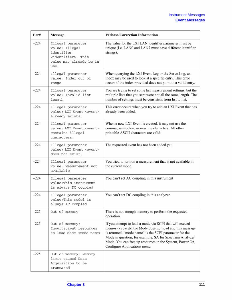
Instrument Messages
Event Messages
–224 Illegal parameter value; Illegal identifier <identifier>. This value may already be in use.
The value for the LXI LAN identifier parameter must be unique (i.e. LAN0 and LAN7 must have different identifier strings).
–224 Illegal parameter value; Index out of range
When querying the LXI Event Log or the Servo Log, an index may be used to look at a specific entry. This error occurs if the index provided does not point to a valid entry.
–224 Illegal parameter value; Invalid list length
You are trying to set some list measurement settings, but the multiple lists that you sent were not all the same length. The number of settings must be consistent from list to list.
–224 Illegal parameter value; LXI Event <event> already exists.
This error occurs when you try to add an LXI Event that has already been added.
–224 Illegal parameter value; LXI Event <event> contains illegal characters.
When a new LXI Event is created, it may not use the comma, semicolon, or newline characters. All other printable ASCII characters are valid.
–224 Illegal parameter value; LXI Event <event> does not exist.
The requested event has not been added yet.
–224 Illegal parameter value; Measurement not available
You tried to turn on a measurement that is not available in the current mode.
–224 Illegal parameter value;This instrument is always DC coupled
You can’t set AC coupling in this instrument
–224 Illegal parameter value;This model is always AC coupled
You can’t set DC coupling in this analyzer
–225 Out of memory There is not enough memory to perform the requested operation.
–225 Out of memory; Insufficient resources to load Mode <mode name>
If you attempt to load a mode via SCPI that will exceed memory capacity, the Mode does not load and this message is returned. “mode name” is the SCPI parameter for the Mode in question, for example, SA for Spectrum Analyzer Mode. You can free up resources in the System, Power On, Configure Applications menu
–225 Out of memory; Memory limit caused Data Acquisition to be truncated
Err# Message Verbose/Correction Information
Chapter 3 111
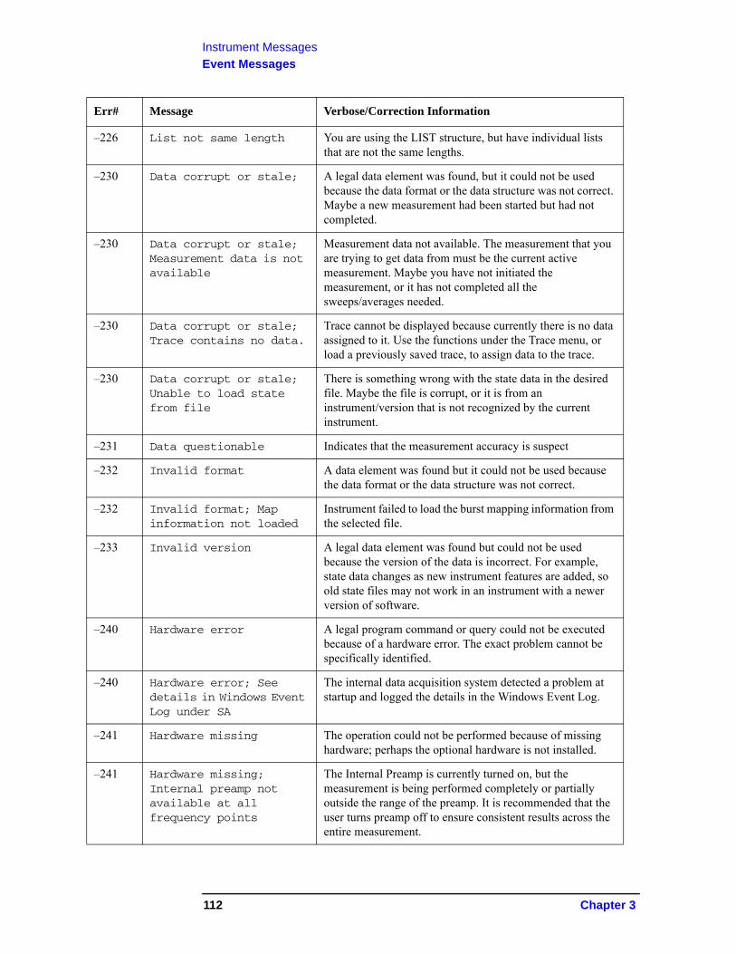
Instrument Messages
Event Messages
–226 List not same length You are using the LIST structure, but have individual lists that are not the same lengths.
–230 Data corrupt or stale; A legal data element was found, but it could not be used because the data format or the data structure was not correct. Maybe a new measurement had been started but had not completed.
–230 Data corrupt or stale; Measurement data is not available
Measurement data not available. The measurement that you are trying to get data from must be the current active measurement. Maybe you have not initiated the measurement, or it has not completed all the sweeps/averages needed.
–230 Data corrupt or stale; Trace contains no data.
Trace cannot be displayed because currently there is no data assigned to it. Use the functions under the Trace menu, or load a previously saved trace, to assign data to the trace.
–230 Data corrupt or stale; Unable to load state from file
There is something wrong with the state data in the desired file. Maybe the file is corrupt, or it is from an instrument/version that is not recognized by the current instrument.
–231 Data questionable Indicates that the measurement accuracy is suspect
–232 Invalid format A data element was found but it could not be used because the data format or the data structure was not correct.
–232 Invalid format; Map information not loaded
Instrument failed to load the burst mapping information from the selected file.
–233 Invalid version A legal data element was found but could not be used because the version of the data is incorrect. For example, state data changes as new instrument features are added, so old state files may not work in an instrument with a newer version of software.
–240 Hardware error A legal program command or query could not be executed because of a hardware error. The exact problem cannot be specifically identified.
–240 Hardware error; See details in Windows Event Log under SA
The internal data acquisition system detected a problem at startup and logged the details in the Windows Event Log.
–241 Hardware missing The operation could not be performed because of missing hardware; perhaps the optional hardware is not installed.
–241 Hardware missing; Internal preamp not available at all frequency points
The Internal Preamp is currently turned on, but the measurement is being performed completely or partially outside the range of the preamp. It is recommended that the user turns preamp off to ensure consistent results across the entire measurement.
Err# Message Verbose/Correction Information
112 Chapter 3
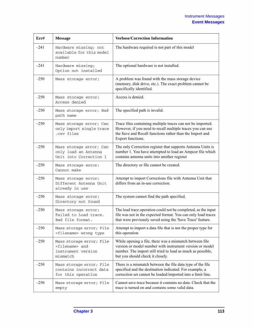
Instrument Messages
Event Messages
–241 Hardware missing; not available for this model number
The hardware required is not part of this model
–241 Hardware missing; Option not installed
The optional hardware is not installed.
–250 Mass storage error; A problem was found with the mass storage device (memory, disk drive, etc.). The exact problem cannot be specifically identified.
–250 Mass storage error; Access denied
Access is denied.
–250 Mass storage error; Bad path name
The specified path is invalid.
–250 Mass storage error; Can only import single trace .csv files
Trace files containing multiple traces can not be imported. However, if you need to recall multiple traces you can use the Save and Recall functions rather than the Import and Export functions.
–250 Mass storage error; Can only load an Antenna Unit into Correction 1
The only Correction register that supports Antenna Units is number 1. You have attempted to load an Ampcor file which contains antenna units into another register
–250 Mass storage error; Cannot make
The directory or file cannot be created.
–250 Mass storage error; Different Antenna Unit already in use
Attempt to import Corrections file with Antenna Unit that differs from an in-use correction.
–250 Mass storage error; Directory not found
The system cannot find the path specified.
–250 Mass storage error; Failed to Load trace. Bad file format.
The load trace operation could not be completed, as the input file was not in the expected format. You can only load traces that were previously saved using the 'Save Trace' feature.
–250 Mass storage error; File <filename> wrong type
Attempt to import a data file that is not the proper type for this operation.
–250 Mass storage error; File <filename> and instrument version mismatch
While opening a file, there was a mismatch between file version or model number with instrument version or model number. The import still tried to load as much as possible, but you should check it closely.
–250 Mass storage error; File contains incorrect data for this operation
There is a mismatch between the file data type of the file specified and the destination indicated. For example, a correction set cannot be loaded/imported into a limit line.
–250 Mass storage error; File empty
Cannot save trace because it contains no data. Check that the trace is turned on and contains some valid data.
Err# Message Verbose/Correction Information
Chapter 3 113
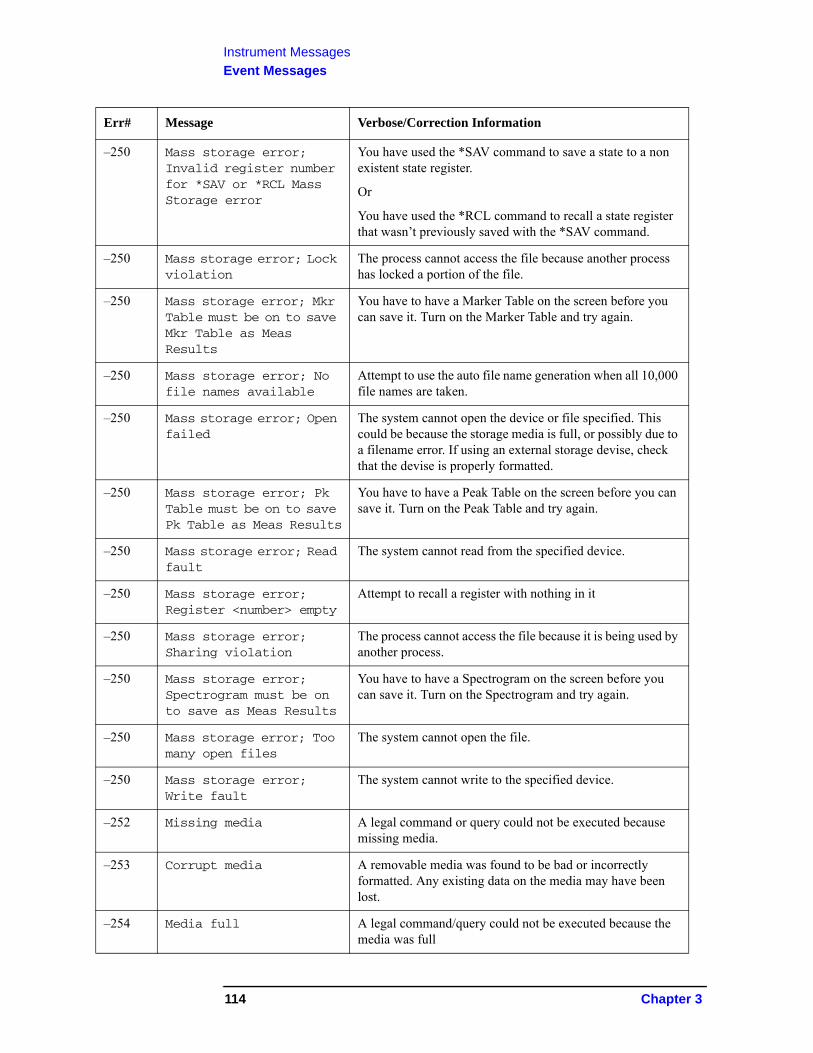
Instrument Messages
Event Messages
–250 Mass storage error; Invalid register number for *SAV or *RCL Mass Storage error
You have used the *SAV command to save a state to a non existent state register.
Or
You have used the *RCL command to recall a state register that wasn’t previously saved with the *SAV command.
–250 Mass storage error; Lock violation
The process cannot access the file because another process has locked a portion of the file.
–250 Mass storage error; Mkr Table must be on to save Mkr Table as Meas Results
You have to have a Marker Table on the screen before you can save it. Turn on the Marker Table and try again.
–250 Mass storage error; No file names available
Attempt to use the auto file name generation when all 10,000 file names are taken.
–250 Mass storage error; Open failed
The system cannot open the device or file specified. This could be because the storage media is full, or possibly due to a filename error. If using an external storage devise, check that the devise is properly formatted.
–250 Mass storage error; Pk Table must be on to save Pk Table as Meas Results
You have to have a Peak Table on the screen before you can save it. Turn on the Peak Table and try again.
–250 Mass storage error; Read fault
The system cannot read from the specified device.
–250 Mass storage error; Register <number> empty
Attempt to recall a register with nothing in it
–250 Mass storage error; Sharing violation
The process cannot access the file because it is being used by another process.
–250 Mass storage error; Spectrogram must be on to save as Meas Results
You have to have a Spectrogram on the screen before you can save it. Turn on the Spectrogram and try again.
–250 Mass storage error; Too many open files
The system cannot open the file.
–250 Mass storage error; Write fault
The system cannot write to the specified device.
–252 Missing media A legal command or query could not be executed because missing media.
–253 Corrupt media A removable media was found to be bad or incorrectly formatted. Any existing data on the media may have been lost.
–254 Media full A legal command/query could not be executed because the media was full
Err# Message Verbose/Correction Information
114 Chapter 3
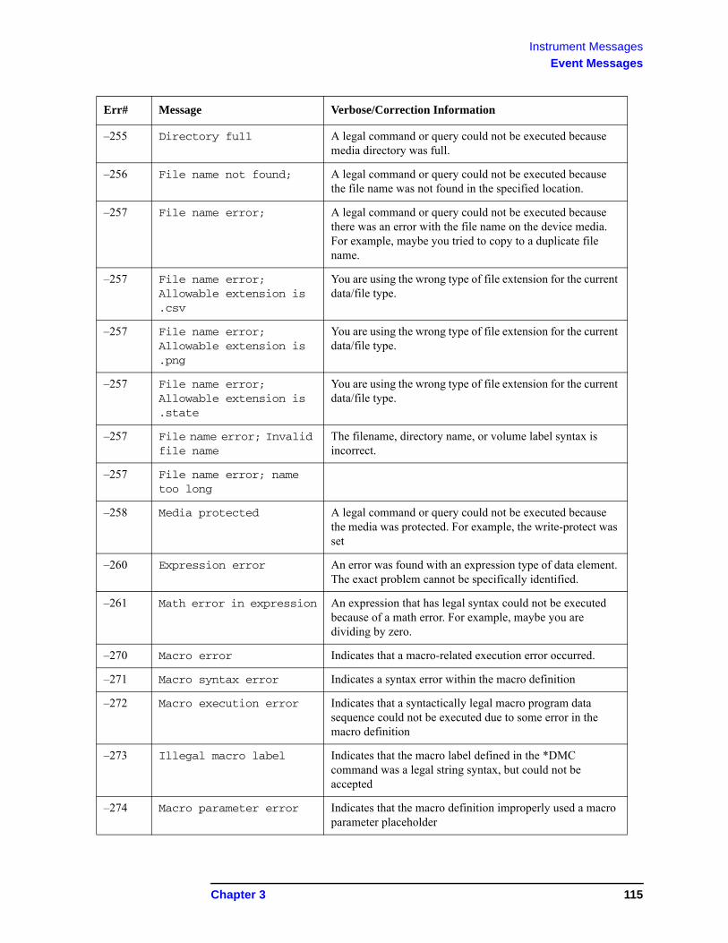
Instrument Messages
Event Messages
–255 Directory full A legal command or query could not be executed because media directory was full.
–256 File name not found; A legal command or query could not be executed because the file name was not found in the specified location.
–257 File name error; A legal command or query could not be executed because there was an error with the file name on the device media. For example, maybe you tried to copy to a duplicate file name.
–257 File name error; Allowable extension is .csv
You are using the wrong type of file extension for the current data/file type.
–257 File name error; Allowable extension is .png
You are using the wrong type of file extension for the current data/file type.
–257 File name error; Allowable extension is .state
You are using the wrong type of file extension for the current data/file type.
–257 File name error; Invalid file name
The filename, directory name, or volume label syntax is incorrect.
–257 File name error; name too long
–258 Media protected A legal command or query could not be executed because the media was protected. For example, the write-protect was set
–260 Expression error An error was found with an expression type of data element. The exact problem cannot be specifically identified.
–261 Math error in expression An expression that has legal syntax could not be executed because of a math error. For example, maybe you are dividing by zero.
–270 Macro error Indicates that a macro-related execution error occurred.
–271 Macro syntax error Indicates a syntax error within the macro definition
–272 Macro execution error Indicates that a syntactically legal macro program data sequence could not be executed due to some error in the macro definition
–273 Illegal macro label Indicates that the macro label defined in the *DMC command was a legal string syntax, but could not be accepted
–274 Macro parameter error Indicates that the macro definition improperly used a macro parameter placeholder
Err# Message Verbose/Correction Information
Chapter 3 115
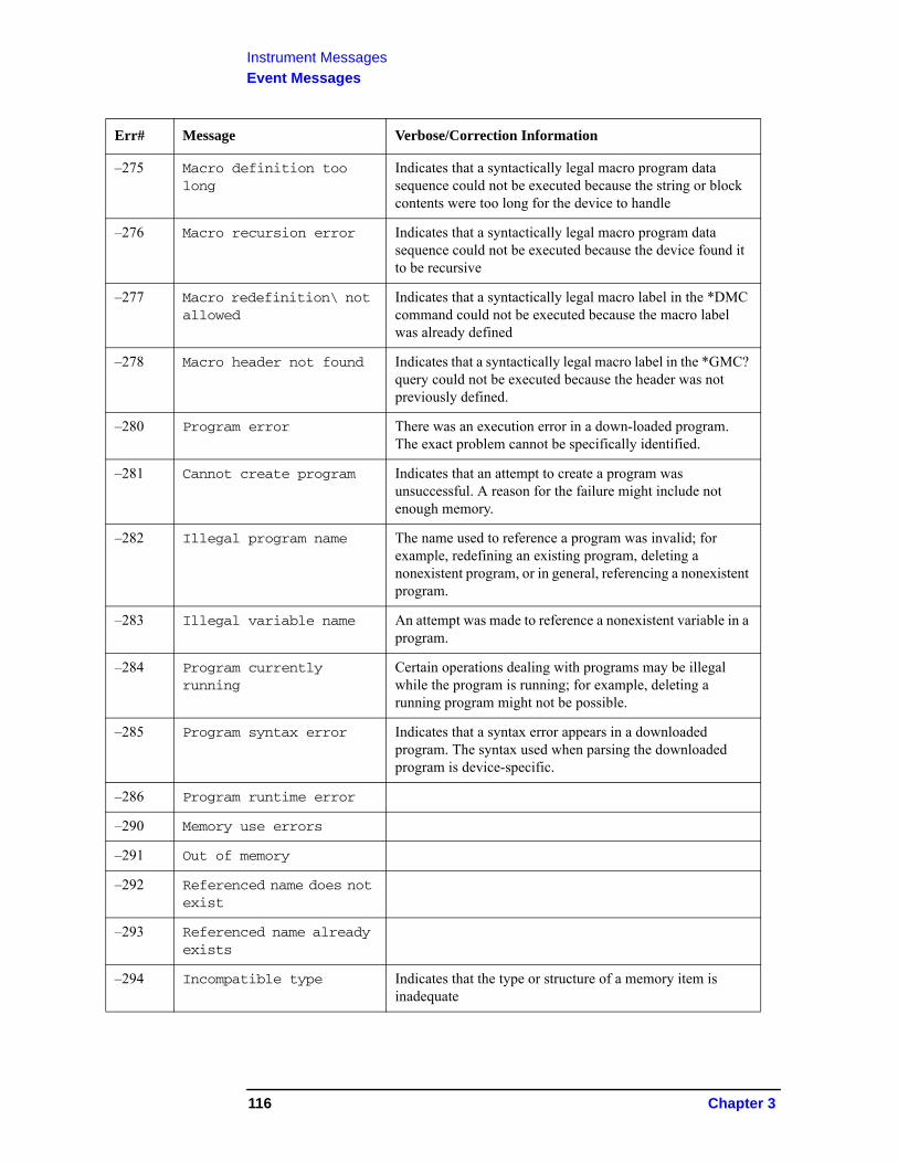
Instrument Messages
Event Messages
–275 Macro definition too long
Indicates that a syntactically legal macro program data sequence could not be executed because the string or block contents were too long for the device to handle
–276 Macro recursion error Indicates that a syntactically legal macro program data sequence could not be executed because the device found it to be recursive
–277 Macro redefinition\ not allowed
Indicates that a syntactically legal macro label in the *DMC command could not be executed because the macro label was already defined
–278 Macro header not found Indicates that a syntactically legal macro label in the *GMC? query could not be executed because the header was not previously defined.
–280 Program error There was an execution error in a down-loaded program. The exact problem cannot be specifically identified.
–281 Cannot create program Indicates that an attempt to create a program was unsuccessful. A reason for the failure might include not enough memory.
–282 Illegal program name The name used to reference a program was invalid; for example, redefining an existing program, deleting a nonexistent program, or in general, referencing a nonexistent program.
–283 Illegal variable name An attempt was made to reference a nonexistent variable in a program.
–284 Program currently running
Certain operations dealing with programs may be illegal while the program is running; for example, deleting a running program might not be possible.
–285 Program syntax error Indicates that a syntax error appears in a downloaded program. The syntax used when parsing the downloaded program is device-specific.
–286 Program runtime error
–290 Memory use errors
–291 Out of memory
–292 Referenced name does not exist
–293 Referenced name already exists
–294 Incompatible type Indicates that the type or structure of a memory item is inadequate
Err# Message Verbose/Correction Information
116 Chapter 3
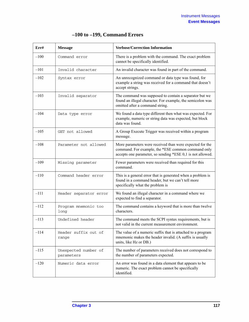
Instrument Messages
Event Messages
–100 to –199, Command Errors
Err# Message Verbose/Correction Information
–100 Command error There is a problem with the command. The exact problem cannot be specifically identified.
–101 Invalid character An invalid character was found in part of the command.
–102 Syntax error An unrecognized command or data type was found, for example a string was received for a command that doesn’t accept strings.
–103 Invalid separator The command was supposed to contain a separator but we found an illegal character. For example, the semicolon was omitted after a command string.
–104 Data type error We found a data type different then what was expected. For example, numeric or string data was expected, but block data was found.
–105 GET not allowed A Group Execute Trigger was received within a program message.
–108 Parameter not allowed More parameters were received than were expected for the command. For example, the *ESE common command only accepts one parameter, so sending *ESE 0,1 is not allowed.
–109 Missing parameter Fewer parameters were received than required for this command.
–110 Command header error This is a general error that is generated when a problem is found in a command header, but we can’t tell more specifically what the problem is
–111 Header separator error We found an illegal character in a command where we expected to find a separator.
–112 Program mnemonic too long
The command contains a keyword that is more than twelve characters.
–113 Undefined header The command meets the SCPI syntax requirements, but is not valid in the current measurement environment.
–114 Header suffix out of range
The value of a numeric suffix that is attached to a program mnemonic makes the header invalid. (A suffix is usually units, like Hz or DB.)
–115 Unexpected number of parameters
The number of parameters received does not correspond to the number of parameters expected.
–120 Numeric data error An error was found in a data element that appears to be numeric. The exact problem cannot be specifically identified.
Chapter 3 117
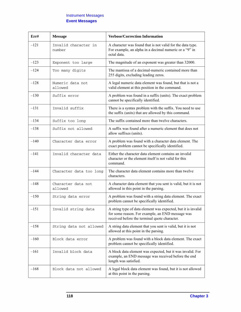
Instrument Messages
Event Messages
–121 Invalid character in number
A character was found that is not valid for the data type. For example, an alpha in a decimal numeric or a “9” in octal data.
–123 Exponent too large The magnitude of an exponent was greater than 32000.
–124 Too many digits The mantissa of a decimal-numeric contained more than 255 digits, excluding leading zeros.
–128 Numeric data not allowed
A legal numeric data element was found, but that is not a valid element at this position in the command.
–130 Suffix error A problem was found in a suffix (units). The exact problem cannot be specifically identified.
–131 Invalid suffix There is a syntax problem with the suffix. You need to use the suffix (units) that are allowed by this command.
–134 Suffix too long The suffix contained more than twelve characters.
–138 Suffix not allowed A suffix was found after a numeric element that does not allow suffixes (units).
–140 Character data error A problem was found with a character data element. The exact problem cannot be specifically identified.
–141 Invalid character data Either the character data element contains an invalid character or the element itself is not valid for this command.
–144 Character data too long The character data element contains more than twelve characters.
–148 Character data not allowed
A character data element that you sent is valid, but it is not allowed in this point in the parsing.
–150 String data error A problem was found with a string data element. The exact problem cannot be specifically identified.
–151 Invalid string data A string type of data element was expected, but it is invalid for some reason. For example, an END message was received before the terminal quote character.
–158 String data not allowed A string data element that you sent is valid, but it is not allowed at this point in the parsing.
–160 Block data error A problem was found with a block data element. The exact problem cannot be specifically identified.
–161 Invalid block data A block data element was expected, but it was invalid. For example, an END message was received before the end length was satisfied.
–168 Block data not allowed A legal block data element was found, but it is not allowed at this point in the parsing.
Err# Message Verbose/Correction Information
118 Chapter 3
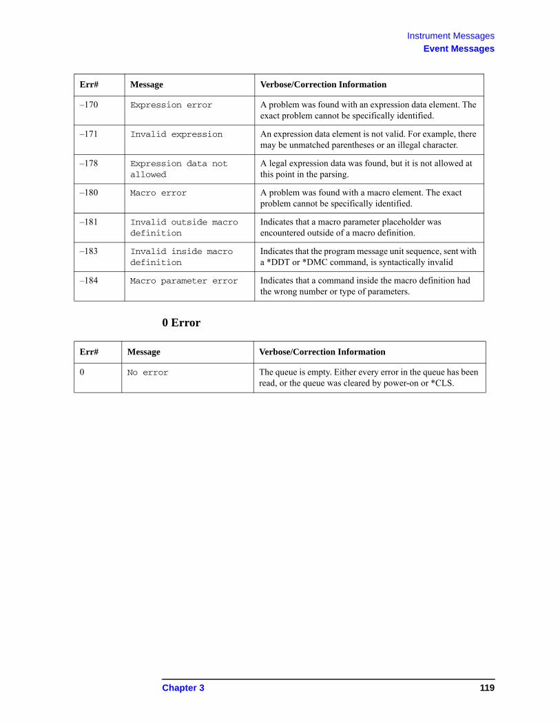
Instrument Messages
Event Messages
0 Error
–170 Expression error A problem was found with an expression data element. The exact problem cannot be specifically identified.
–171 Invalid expression An expression data element is not valid. For example, there may be unmatched parentheses or an illegal character.
–178 Expression data not allowed
A legal expression data was found, but it is not allowed at this point in the parsing.
–180 Macro error A problem was found with a macro element. The exact problem cannot be specifically identified.
–181 Invalid outside macro definition
Indicates that a macro parameter placeholder was encountered outside of a macro definition.
–183 Invalid inside macro definition
Indicates that the program message unit sequence, sent with a *DDT or *DMC command, is syntactically invalid
–184 Macro parameter error Indicates that a command inside the macro definition had the wrong number or type of parameters.
Err# Message Verbose/Correction Information
Err# Message Verbose/Correction Information
0 No error The queue is empty. Either every error in the queue has been read, or the queue was cleared by power-on or *CLS.
Chapter 3 119
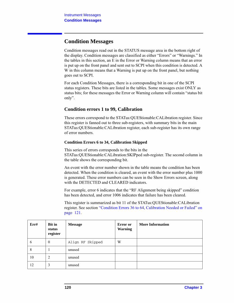
Instrument Messages
Condition Messages
Condition Messages
Condition messages read out in the STATUS message area in the bottom right of the display. Condition messages are classified as either “Errors” or “Warnings.” In the tables in this section, an E in the Error or Warning column means that an error is put up on the front panel and sent out to SCPI when this condition is detected. A W in this column means that a Warning is put up on the front panel, but nothing goes out to SCPI.
For each Condition Messages, there is a corresponding bit in one of the SCPI status registers. These bits are listed in the tables. Some messages exist ONLY as status bits; for these messages the Error or Warning column will contain “status bit only”.
Condition errors 1 to 99, Calibration
These errors correspond to the STATus:QUEStionable:CALibration register. Since this register is fanned out to three sub-registers, with summary bits in the main STATus:QUEStionable:CALibration register, each sub-register has its own range of error numbers.
Condition Errors 6 to 34, Calibration Skipped
This series of errors corresponds to the bits in the STATus:QUEStionable:CALibration:SKIPped sub-register. The second column in the table shows the corresponding bit.
An event with the error number shown in the table means the condition has been detected. When the condition is cleared, an event with the error number plus 1000 is generated. These error numbers can be seen in the Show Errors screen, along with the DETECTED and CLEARED indicators.
For example, error 6 indicates that the “RF Alignment being skipped” condition has been detected, and error 1006 indicates that failure has been cleared.
This register is summarized as bit 11 of the STATus:QUEStionable:CALibration register. See section “Condition Errors 36 to 64, Calibration Needed or Failed” on page 121.
Err# Bit in status register
Message Error or Warning
More Information
6 0 Align RF Skipped W
8 1 unused
10 2 unused
12 3 unused
120 Chapter 3
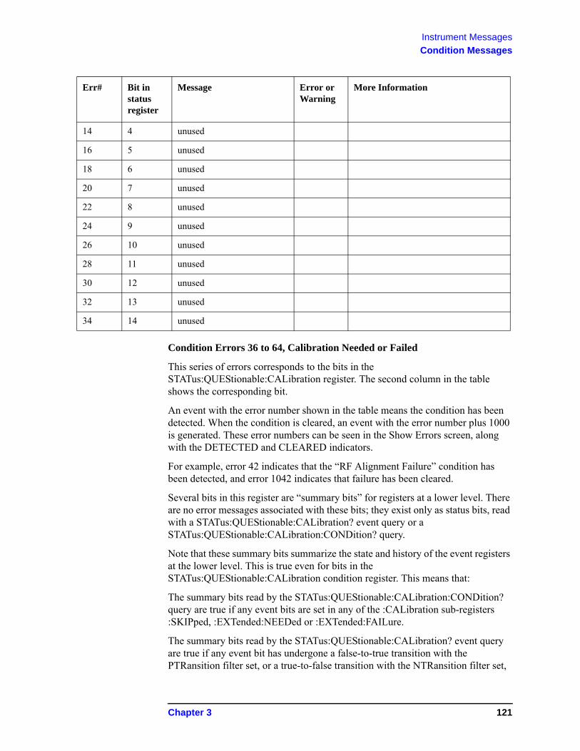
Instrument Messages
Condition Messages
Condition Errors 36 to 64, Calibration Needed or Failed
This series of errors corresponds to the bits in the STATus:QUEStionable:CALibration register. The second column in the table shows the corresponding bit.
An event with the error number shown in the table means the condition has been detected. When the condition is cleared, an event with the error number plus 1000 is generated. These error numbers can be seen in the Show Errors screen, along with the DETECTED and CLEARED indicators.
For example, error 42 indicates that the “RF Alignment Failure” condition has been detected, and error 1042 indicates that failure has been cleared.
Several bits in this register are “summary bits” for registers at a lower level. There are no error messages associated with these bits; they exist only as status bits, read with a STATus:QUEStionable:CALibration? event query or a STATus:QUEStionable:CALibration:CONDition? query.
Note that these summary bits summarize the state and history of the event registers at the lower level. This is true even for bits in the STATus:QUEStionable:CALibration condition register. This means that:
The summary bits read by the STATus:QUEStionable:CALibration:CONDition? query are true if any event bits are set in any of the :CALibration sub-registers :SKIPped, :EXTended:NEEDed or :EXTended:FAILure.
The summary bits read by the STATus:QUEStionable:CALibration? event query are true if any event bit has undergone a false-to-true transition with the PTRansition filter set, or a true-to-false transition with the NTRansition filter set,
14 4 unused
16 5 unused
18 6 unused
20 7 unused
22 8 unused
24 9 unused
26 10 unused
28 11 unused
30 12 unused
32 13 unused
34 14 unused
Err# Bit in status register
Message Error or Warning
More Information
Chapter 3 121
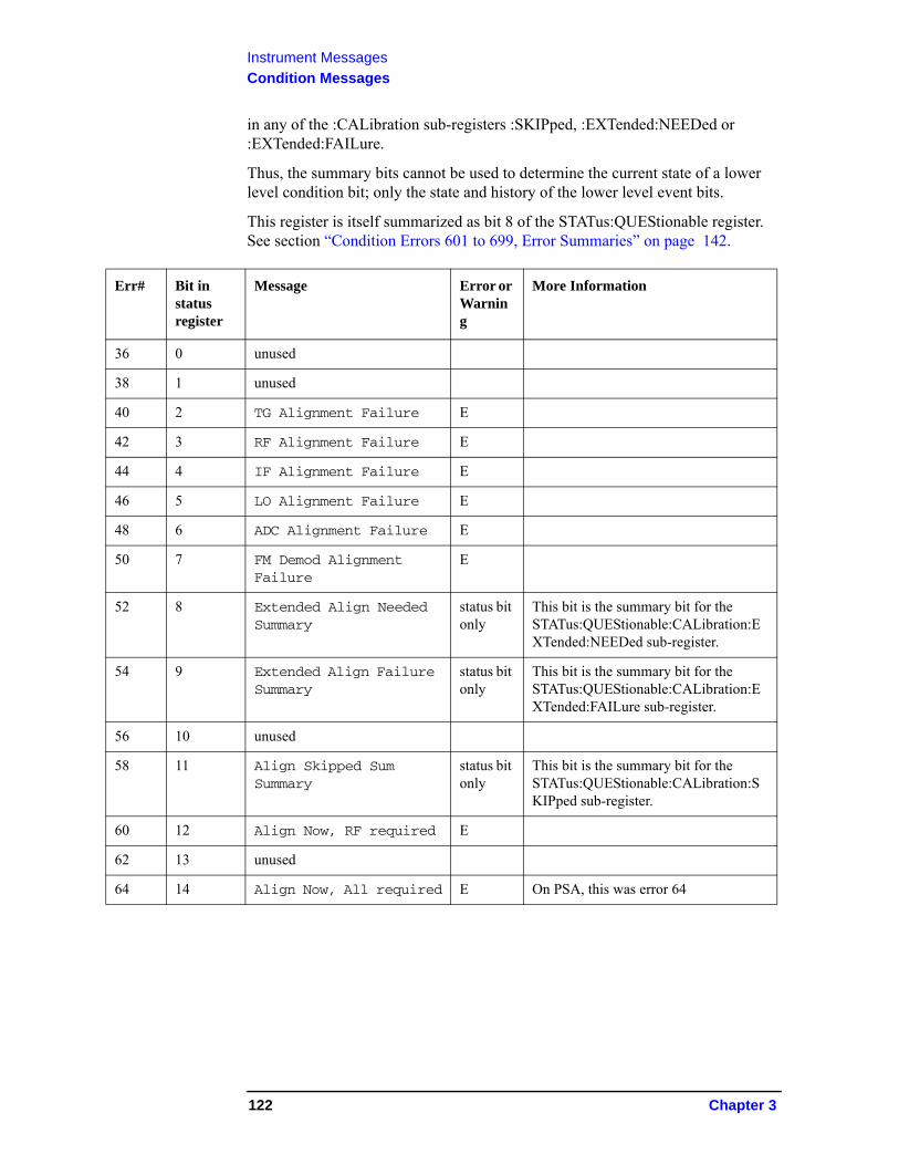
Instrument Messages
Condition Messages
in any of the :CALibration sub-registers :SKIPped, :EXTended:NEEDed or :EXTended:FAILure.
Thus, the summary bits cannot be used to determine the current state of a lower level condition bit; only the state and history of the lower level event bits.
This register is itself summarized as bit 8 of the STATus:QUEStionable register. See section “Condition Errors 601 to 699, Error Summaries” on page 142.
Err# Bit in status register
Message Error or Warning
More Information
36 0 unused
38 1 unused
40 2 TG Alignment Failure E
42 3 RF Alignment Failure E
44 4 IF Alignment Failure E
46 5 LO Alignment Failure E
48 6 ADC Alignment Failure E
50 7 FM Demod Alignment Failure
E
52 8 Extended Align Needed Summary
status bit only
This bit is the summary bit for the STATus:QUEStionable:CALibration:EXTended:NEEDed sub-register.
54 9 Extended Align Failure Summary
status bit only
This bit is the summary bit for the STATus:QUEStionable:CALibration:EXTended:FAILure sub-register.
56 10 unused
58 11 Align Skipped Sum Summary
status bit only
This bit is the summary bit for the STATus:QUEStionable:CALibration:SKIPped sub-register.
60 12 Align Now, RF required E
62 13 unused
64 14 Align Now, All required E On PSA, this was error 64
122 Chapter 3
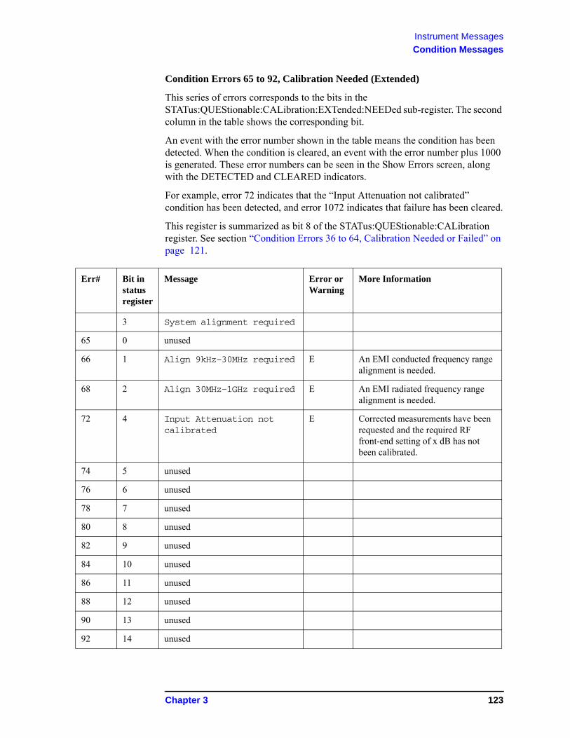
Instrument Messages
Condition Messages
Condition Errors 65 to 92, Calibration Needed (Extended)
This series of errors corresponds to the bits in the STATus:QUEStionable:CALibration:EXTended:NEEDed sub-register. The second column in the table shows the corresponding bit.
An event with the error number shown in the table means the condition has been detected. When the condition is cleared, an event with the error number plus 1000 is generated. These error numbers can be seen in the Show Errors screen, along with the DETECTED and CLEARED indicators.
For example, error 72 indicates that the “Input Attenuation not calibrated” condition has been detected, and error 1072 indicates that failure has been cleared.
This register is summarized as bit 8 of the STATus:QUEStionable:CALibration register. See section “Condition Errors 36 to 64, Calibration Needed or Failed” on page 121.
Err# Bit in status register
Message Error or Warning
More Information
3 System alignment required
65 0 unused
66 1 Align 9kHz–30MHz required E An EMI conducted frequency range alignment is needed.
68 2 Align 30MHz–1GHz required E An EMI radiated frequency range alignment is needed.
72 4 Input Attenuation not calibrated
E Corrected measurements have been requested and the required RF front-end setting of x dB has not been calibrated.
74 5 unused
76 6 unused
78 7 unused
80 8 unused
82 9 unused
84 10 unused
86 11 unused
88 12 unused
90 13 unused
92 14 unused
Chapter 3 123
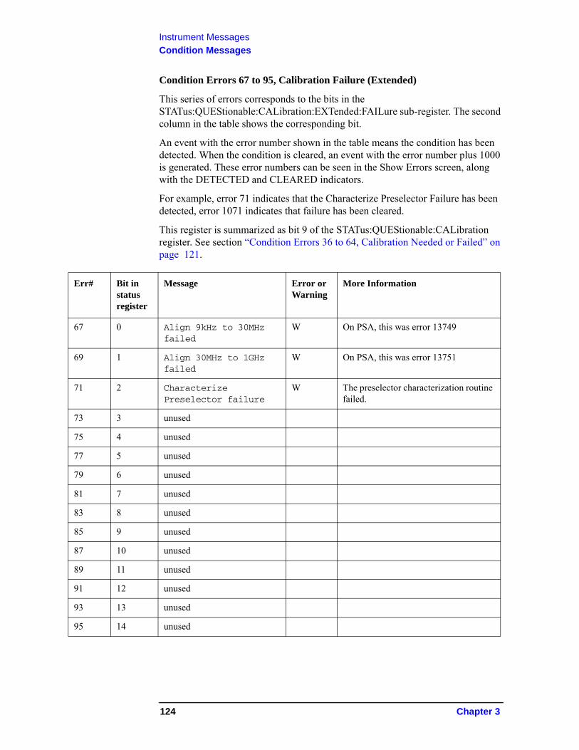
Instrument Messages
Condition Messages
Condition Errors 67 to 95, Calibration Failure (Extended)
This series of errors corresponds to the bits in the STATus:QUEStionable:CALibration:EXTended:FAILure sub-register. The second column in the table shows the corresponding bit.
An event with the error number shown in the table means the condition has been detected. When the condition is cleared, an event with the error number plus 1000 is generated. These error numbers can be seen in the Show Errors screen, along with the DETECTED and CLEARED indicators.
For example, error 71 indicates that the Characterize Preselector Failure has been detected, error 1071 indicates that failure has been cleared.
This register is summarized as bit 9 of the STATus:QUEStionable:CALibration register. See section “Condition Errors 36 to 64, Calibration Needed or Failed” on page 121.
Err# Bit in status register
Message Error or Warning
More Information
67 0 Align 9kHz to 30MHz failed
W On PSA, this was error 13749
69 1 Align 30MHz to 1GHz failed
W On PSA, this was error 13751
71 2 Characterize Preselector failure
W The preselector characterization routine failed.
73 3 unused
75 4 unused
77 5 unused
79 6 unused
81 7 unused
83 8 unused
85 9 unused
87 10 unused
89 11 unused
91 12 unused
93 13 unused
95 14 unused
124 Chapter 3
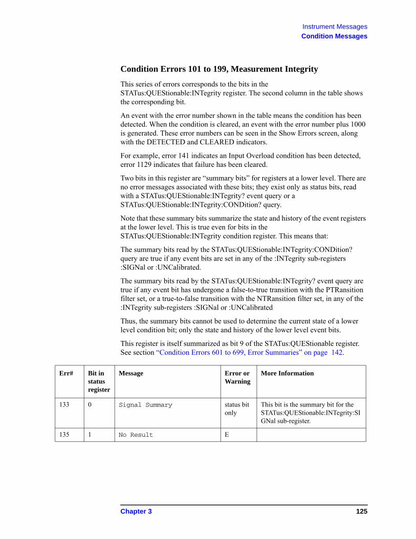
Instrument Messages
Condition Messages
Condition Errors 101 to 199, Measurement Integrity
This series of errors corresponds to the bits in the STATus:QUEStionable:INTegrity register. The second column in the table shows the corresponding bit.
An event with the error number shown in the table means the condition has been detected. When the condition is cleared, an event with the error number plus 1000 is generated. These error numbers can be seen in the Show Errors screen, along with the DETECTED and CLEARED indicators.
For example, error 141 indicates an Input Overload condition has been detected, error 1129 indicates that failure has been cleared.
Two bits in this register are “summary bits” for registers at a lower level. There are no error messages associated with these bits; they exist only as status bits, read with a STATus:QUEStionable:INTegrity? event query or a STATus:QUEStionable:INTegrity:CONDition? query.
Note that these summary bits summarize the state and history of the event registers at the lower level. This is true even for bits in the STATus:QUEStionable:INTegrity condition register. This means that:
The summary bits read by the STATus:QUEStionable:INTegrity:CONDition? query are true if any event bits are set in any of the :INTegrity sub-registers :SIGNal or :UNCalibrated.
The summary bits read by the STATus:QUEStionable:INTegrity? event query are true if any event bit has undergone a false-to-true transition with the PTRansition filter set, or a true-to-false transition with the NTRansition filter set, in any of the :INTegrity sub-registers :SIGNal or :UNCalibrated
Thus, the summary bits cannot be used to determine the current state of a lower level condition bit; only the state and history of the lower level event bits.
This register is itself summarized as bit 9 of the STATus:QUEStionable register. See section “Condition Errors 601 to 699, Error Summaries” on page 142.
Err# Bit in status register
Message Error or Warning
More Information
133 0 Signal Summary status bit only
This bit is the summary bit for the STATus:QUEStionable:INTegrity:SIGNal sub-register.
135 1 No Result E
Chapter 3 125
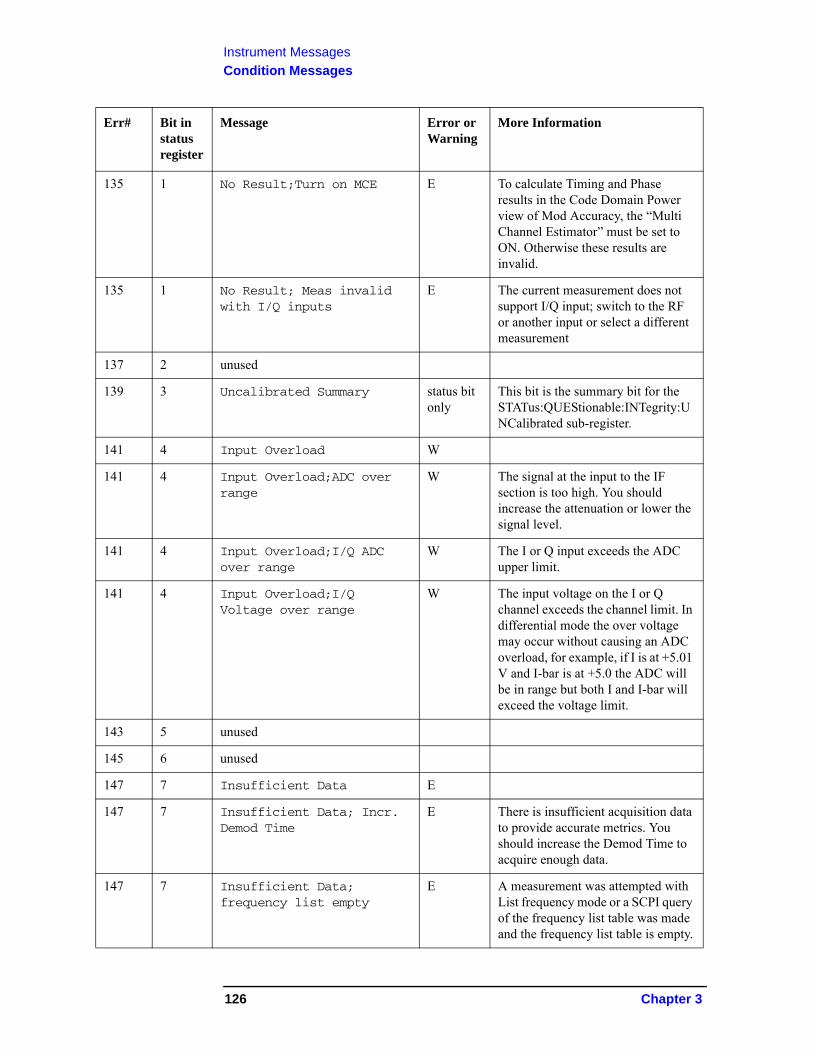
Instrument Messages
Condition Messages
135 1 No Result;Turn on MCE E To calculate Timing and Phase results in the Code Domain Power view of Mod Accuracy, the “Multi Channel Estimator” must be set to ON. Otherwise these results are invalid.
135 1 No Result; Meas invalid with I/Q inputs
E The current measurement does not support I/Q input; switch to the RF or another input or select a different measurement
137 2 unused
139 3 Uncalibrated Summary status bit only
This bit is the summary bit for the STATus:QUEStionable:INTegrity:UNCalibrated sub-register.
141 4 Input Overload W
141 4 Input Overload;ADC over range
W The signal at the input to the IF section is too high. You should increase the attenuation or lower the signal level.
141 4 Input Overload;I/Q ADC over range
W The I or Q input exceeds the ADC upper limit.
141 4 Input Overload;I/Q Voltage over range
W The input voltage on the I or Q channel exceeds the channel limit. In differential mode the over voltage may occur without causing an ADC overload, for example, if I is at +5.01 V and I-bar is at +5.0 the ADC will be in range but both I and I-bar will exceed the voltage limit.
143 5 unused
145 6 unused
147 7 Insufficient Data E
147 7 Insufficient Data; Incr. Demod Time
E There is insufficient acquisition data to provide accurate metrics. You should increase the Demod Time to acquire enough data.
147 7 Insufficient Data; frequency list empty
E A measurement was attempted with List frequency mode or a SCPI query of the frequency list table was made and the frequency list table is empty.
Err# Bit in status register
Message Error or Warning
More Information
126 Chapter 3
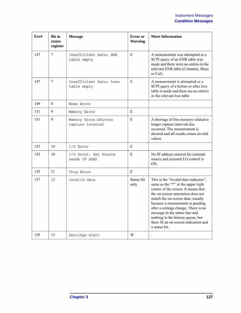
Instrument Messages
Condition Messages
147 7 Insufficient Data; ENR table empty
E A measurement was attempted or a SCPI query of an ENR table was made and there were no entries in the relevant ENR table (Common, Meas or Cal).
147 7 Insufficient Data; Loss table empty
E A measurement is attempted or a SCPI query of a before or after loss table is made and there are no entries in the relevant loss table
149 8 Meas Error
151 9 Memory Error E
151 9 Memory Error;Shorten capture interval
E A shortage of free memory related to longer capture intervals has occurred. The measurement is aborted and all results return invalid values
153 10 I/O Error E
153 10 I/O Error; Ext Source needs IP Addr
E No IP address entered for external source and external LO control is ON.
155 11 Trig Error E
157 12 Invalid Data Status bit only
This is the “invalid data indicator”, same as the “*” in the upper right corner of the screen. It means that the on-screen annotation does not match the on-screen data, usually because a measurement is pending after a settings change. There is no message in the status line and nothing in the history queue, but there IS an on-screen indication and a status bit.
159 13 Settings Alert W .
Err# Bit in status register
Message Error or Warning
More Information
Chapter 3 127
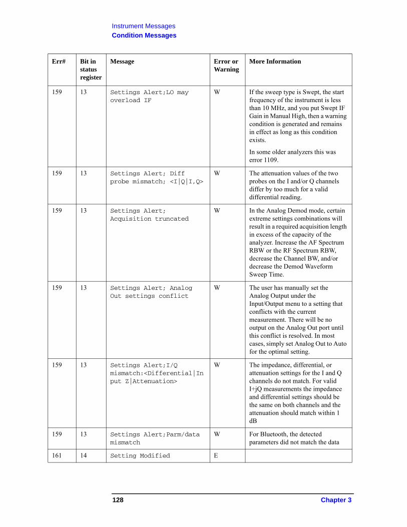
Instrument Messages
Condition Messages
159 13 Settings Alert;LO may overload IF
W If the sweep type is Swept, the start frequency of the instrument is less than 10 MHz, and you put Swept IF Gain in Manual High, then a warning condition is generated and remains in effect as long as this condition exists.
In some older analyzers this was error 1109.
159 13 Settings Alert; Diff probe mismatch; <I|Q|I,Q>
W The attenuation values of the two probes on the I and/or Q channels differ by too much for a valid differential reading.
159 13 Settings Alert; Acquisition truncated
W In the Analog Demod mode, certain extreme settings combinations will result in a required acquisition length in excess of the capacity of the analyzer. Increase the AF Spectrum RBW or the RF Spectrum RBW, decrease the Channel BW, and/or decrease the Demod Waveform Sweep Time.
159 13 Settings Alert; Analog Out settings conflict
W The user has manually set the Analog Output under the Input/Output menu to a setting that conflicts with the current measurement. There will be no output on the Analog Out port until this conflict is resolved. In most cases, simply set Analog Out to Auto for the optimal setting.
159 13 Settings Alert;I/Q mismatch:<Differential|Input Z|Attenuation>
W The impedance, differential, or attenuation settings for the I and Q channels do not match. For valid I+jQ measurements the impedance and differential settings should be the same on both channels and the attenuation should match within 1 dB
159 13 Settings Alert;Parm/data mismatch
W For Bluetooth, the detected parameters did not match the data
161 14 Setting Modified E
Err# Bit in status register
Message Error or Warning
More Information
128 Chapter 3
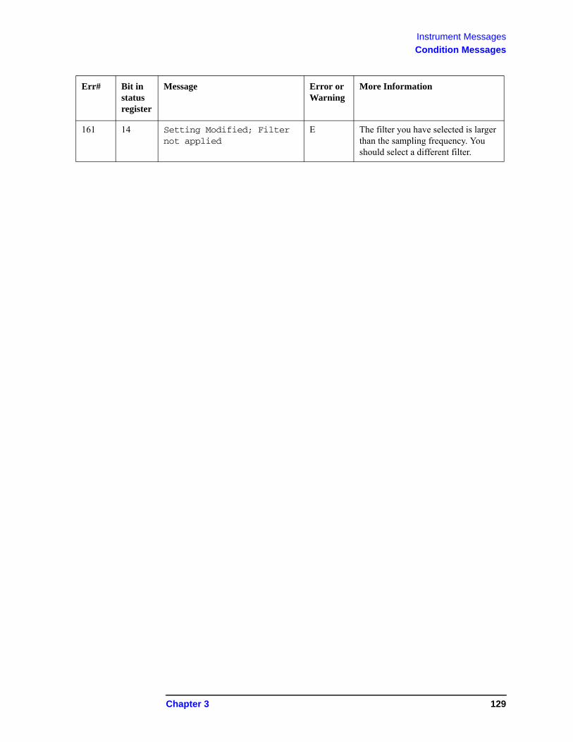
Instrument Messages
Condition Messages
161 14 Setting Modified; Filter not applied
E The filter you have selected is larger than the sampling frequency. You should select a different filter.
Err# Bit in status register
Message Error or Warning
More Information
Chapter 3 129
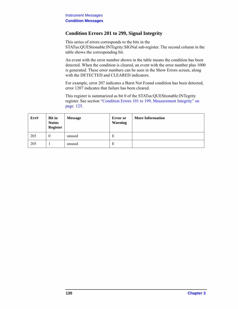
Instrument Messages
Condition Messages
Condition Errors 201 to 299, Signal Integrity
This series of errors corresponds to the bits in the STATus:QUEStionable:INTegrity:SIGNal sub-register. The second column in the table shows the corresponding bit.
An event with the error number shown in the table means the condition has been detected. When the condition is cleared, an event with the error number plus 1000 is generated. These error numbers can be seen in the Show Errors screen, along with the DETECTED and CLEARED indicators.
For example, error 207 indicates a Burst Not Found condition has been detected, error 1207 indicates that failure has been cleared.
This register is summarized as bit 0 of the STATus:QUEStionable:INTegrity register. See section “Condition Errors 101 to 199, Measurement Integrity” on page 125.
Err# Bit in Status Register
Message Error or Warning
More Information
203 0 unused E
205 1 unused E
130 Chapter 3
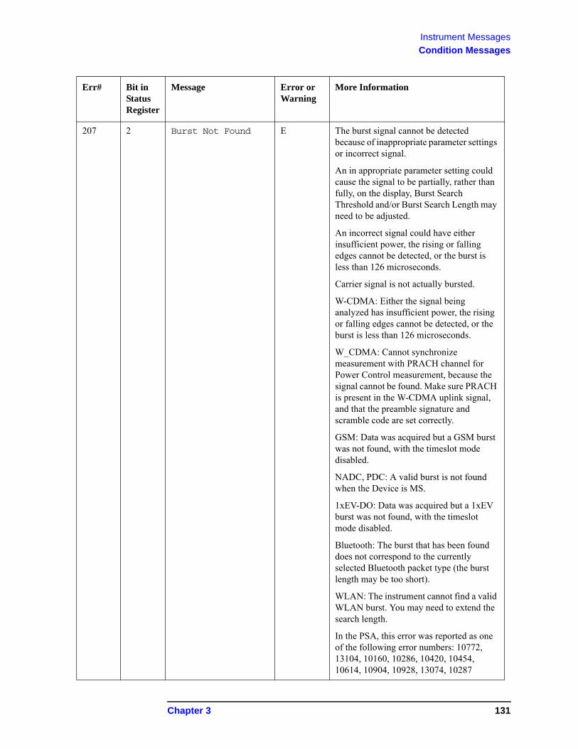
Instrument Messages
Condition Messages
207 2 Burst Not Found E The burst signal cannot be detected because of inappropriate parameter settings or incorrect signal.
An in appropriate parameter setting could cause the signal to be partially, rather than fully, on the display, Burst Search Threshold and/or Burst Search Length may need to be adjusted.
An incorrect signal could have either insufficient power, the rising or falling edges cannot be detected, or the burst is less than 126 microseconds.
Carrier signal is not actually bursted.
W-CDMA: Either the signal being analyzed has insufficient power, the rising or falling edges cannot be detected, or the burst is less than 126 microseconds.
W_CDMA: Cannot synchronize measurement with PRACH channel for Power Control measurement, because the signal cannot be found. Make sure PRACH is present in the W-CDMA uplink signal, and that the preamble signature and scramble code are set correctly.
GSM: Data was acquired but a GSM burst was not found, with the timeslot mode disabled.
NADC, PDC: A valid burst is not found when the Device is MS.
1xEV-DO: Data was acquired but a 1xEV burst was not found, with the timeslot mode disabled.
Bluetooth: The burst that has been found does not correspond to the currently selected Bluetooth packet type (the burst length may be too short).
WLAN: The instrument cannot find a valid WLAN burst. You may need to extend the search length.
In the PSA, this error was reported as one of the following error numbers: 10772, 13104, 10160, 10286, 10420, 10454, 10614, 10904, 10928, 13074, 10287
Err# Bit in Status Register
Message Error or Warning
More Information
Chapter 3 131
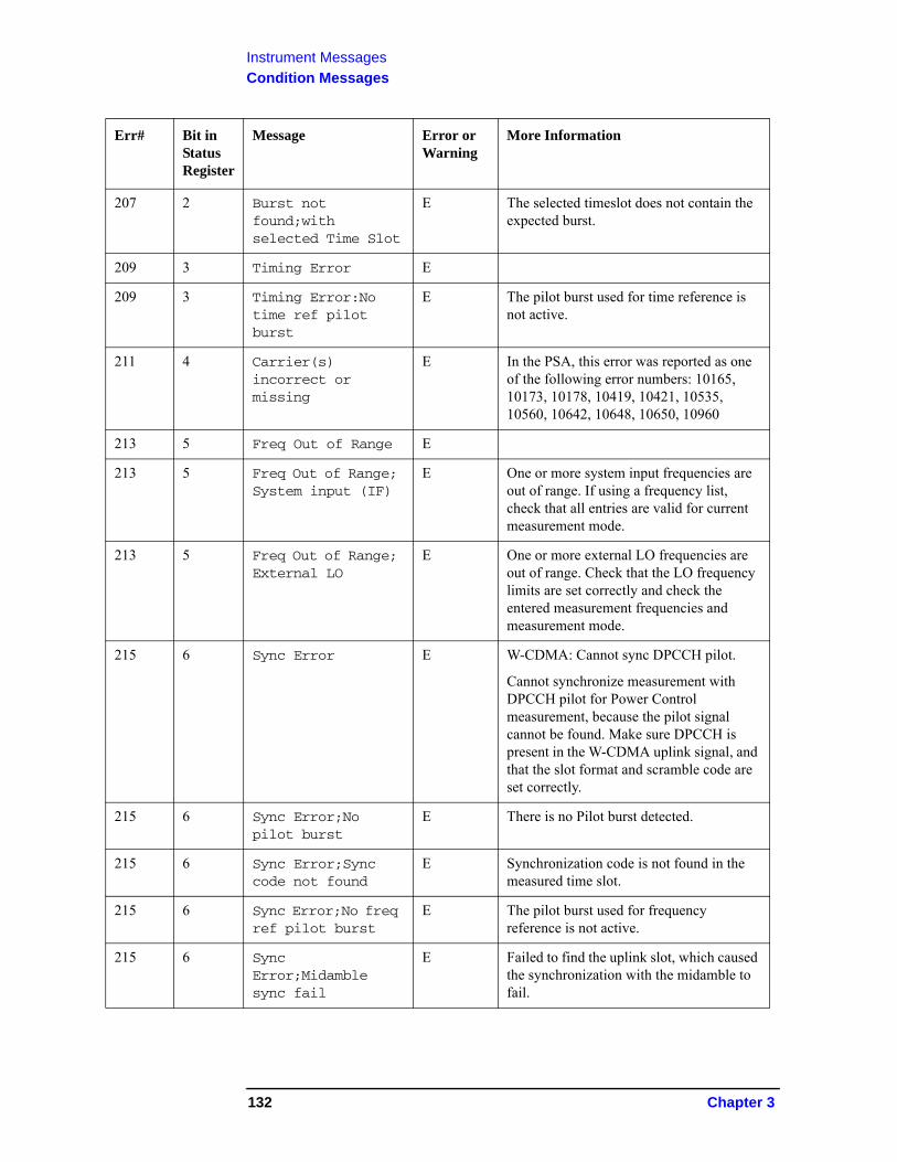
Instrument Messages
Condition Messages
207 2 Burst not found;with selected Time Slot
E The selected timeslot does not contain the expected burst.
209 3 Timing Error E
209 3 Timing Error:No time ref pilot burst
E The pilot burst used for time reference is not active.
211 4 Carrier(s) incorrect or missing
E In the PSA, this error was reported as one of the following error numbers: 10165, 10173, 10178, 10419, 10421, 10535, 10560, 10642, 10648, 10650, 10960
213 5 Freq Out of Range E
213 5 Freq Out of Range; System input (IF)
E One or more system input frequencies are out of range. If using a frequency list, check that all entries are valid for current measurement mode.
213 5 Freq Out of Range; External LO
E One or more external LO frequencies are out of range. Check that the LO frequency limits are set correctly and check the entered measurement frequencies and measurement mode.
215 6 Sync Error E W-CDMA: Cannot sync DPCCH pilot.
Cannot synchronize measurement with DPCCH pilot for Power Control measurement, because the pilot signal cannot be found. Make sure DPCCH is present in the W-CDMA uplink signal, and that the slot format and scramble code are set correctly.
215 6 Sync Error;No pilot burst
E There is no Pilot burst detected.
215 6 Sync Error;Sync code not found
E Synchronization code is not found in the measured time slot.
215 6 Sync Error;No freq ref pilot burst
E The pilot burst used for frequency reference is not active.
215 6 Sync Error;Midamble sync fail
E Failed to find the uplink slot, which caused the synchronization with the midamble to fail.
Err# Bit in Status Register
Message Error or Warning
More Information
132 Chapter 3
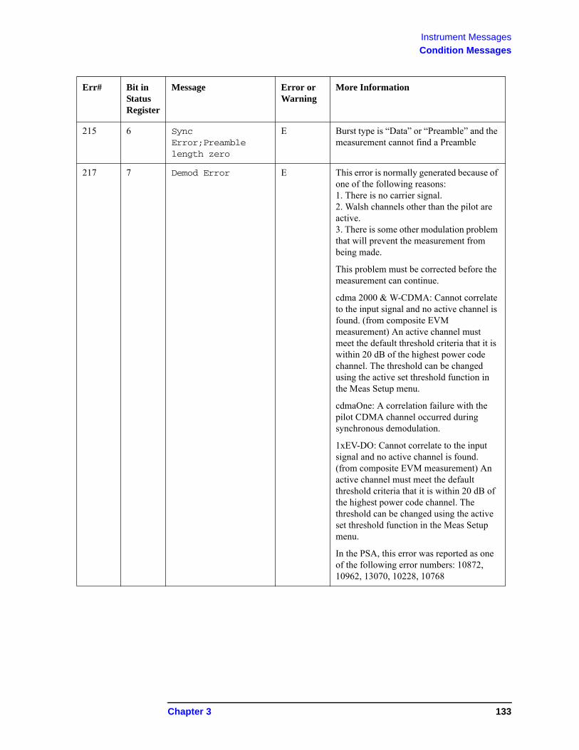
Instrument Messages
Condition Messages
215 6 Sync Error;Preamble length zero
E Burst type is “Data” or “Preamble” and the measurement cannot find a Preamble
217 7 Demod Error E This error is normally generated because of one of the following reasons: 1. There is no carrier signal.2. Walsh channels other than the pilot are active. 3. There is some other modulation problem that will prevent the measurement from being made.
This problem must be corrected before the measurement can continue.
cdma 2000 & W-CDMA: Cannot correlate to the input signal and no active channel is found. (from composite EVM measurement) An active channel must meet the default threshold criteria that it is within 20 dB of the highest power code channel. The threshold can be changed using the active set threshold function in the Meas Setup menu.
cdmaOne: A correlation failure with the pilot CDMA channel occurred during synchronous demodulation.
1xEV-DO: Cannot correlate to the input signal and no active channel is found. (from composite EVM measurement) An active channel must meet the default threshold criteria that it is within 20 dB of the highest power code channel. The threshold can be changed using the active set threshold function in the Meas Setup menu.
In the PSA, this error was reported as one of the following error numbers: 10872, 10962, 13070, 10228, 10768
Err# Bit in Status Register
Message Error or Warning
More Information
Chapter 3 133
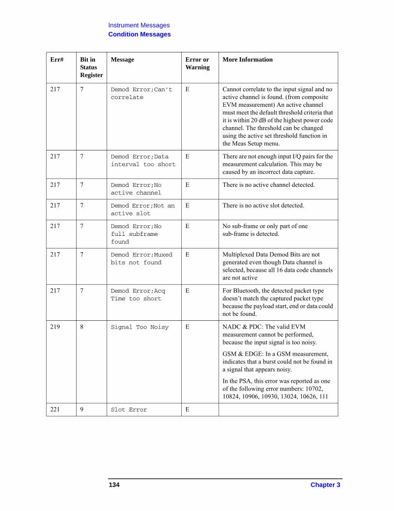
Instrument Messages
Condition Messages
217 7 Demod Error;Can’t correlate
E Cannot correlate to the input signal and no active channel is found. (from composite EVM measurement) An active channel must meet the default threshold criteria that it is within 20 dB of the highest power code channel. The threshold can be changed using the active set threshold function in the Meas Setup menu.
217 7 Demod Error;Data interval too short
E There are not enough input I/Q pairs for the measurement calculation. This may be caused by an incorrect data capture.
217 7 Demod Error;No active channel
E There is no active channel detected.
217 7 Demod Error;Not an active slot
E There is no active slot detected.
217 7 Demod Error;No full subframe found
E No sub-frame or only part of one sub-frame is detected.
217 7 Demod Error;Muxed bits not found
E Multiplexed Data Demod Bits are not generated even though Data channel is selected, because all 16 data code channels are not active
217 7 Demod Error;Acq Time too short
E For Bluetooth, the detected packet type doesn’t match the captured packet type because the payload start, end or data could not be found.
219 8 Signal Too Noisy E NADC & PDC: The valid EVM measurement cannot be performed, because the input signal is too noisy.
GSM & EDGE: In a GSM measurement, indicates that a burst could not be found in a signal that appears noisy.
In the PSA, this error was reported as one of the following error numbers: 10702, 10824, 10906, 10930, 13024, 10626, 111
221 9 Slot Error E
Err# Bit in Status Register
Message Error or Warning
More Information
134 Chapter 3
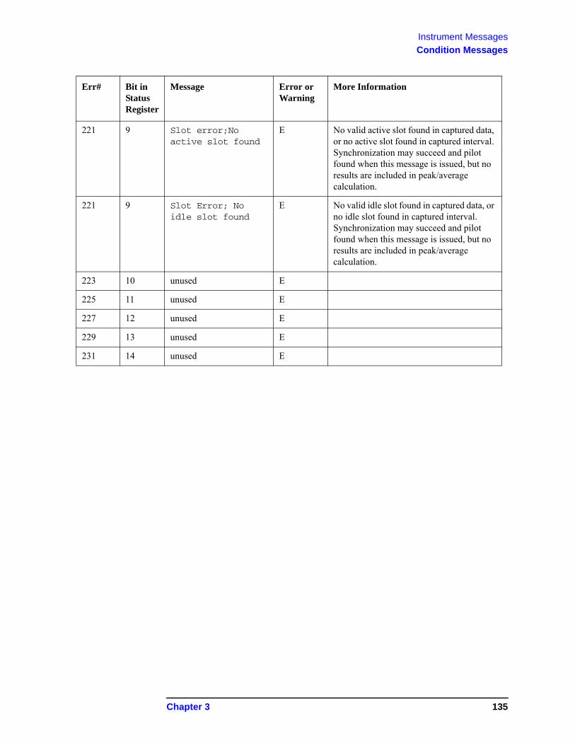
Instrument Messages
Condition Messages
221 9 Slot error;No active slot found
E No valid active slot found in captured data, or no active slot found in captured interval. Synchronization may succeed and pilot found when this message is issued, but no results are included in peak/average calculation.
221 9 Slot Error; No idle slot found
E No valid idle slot found in captured data, or no idle slot found in captured interval. Synchronization may succeed and pilot found when this message is issued, but no results are included in peak/average calculation.
223 10 unused E
225 11 unused E
227 12 unused E
229 13 unused E
231 14 unused E
Err# Bit in Status Register
Message Error or Warning
More Information
Chapter 3 135
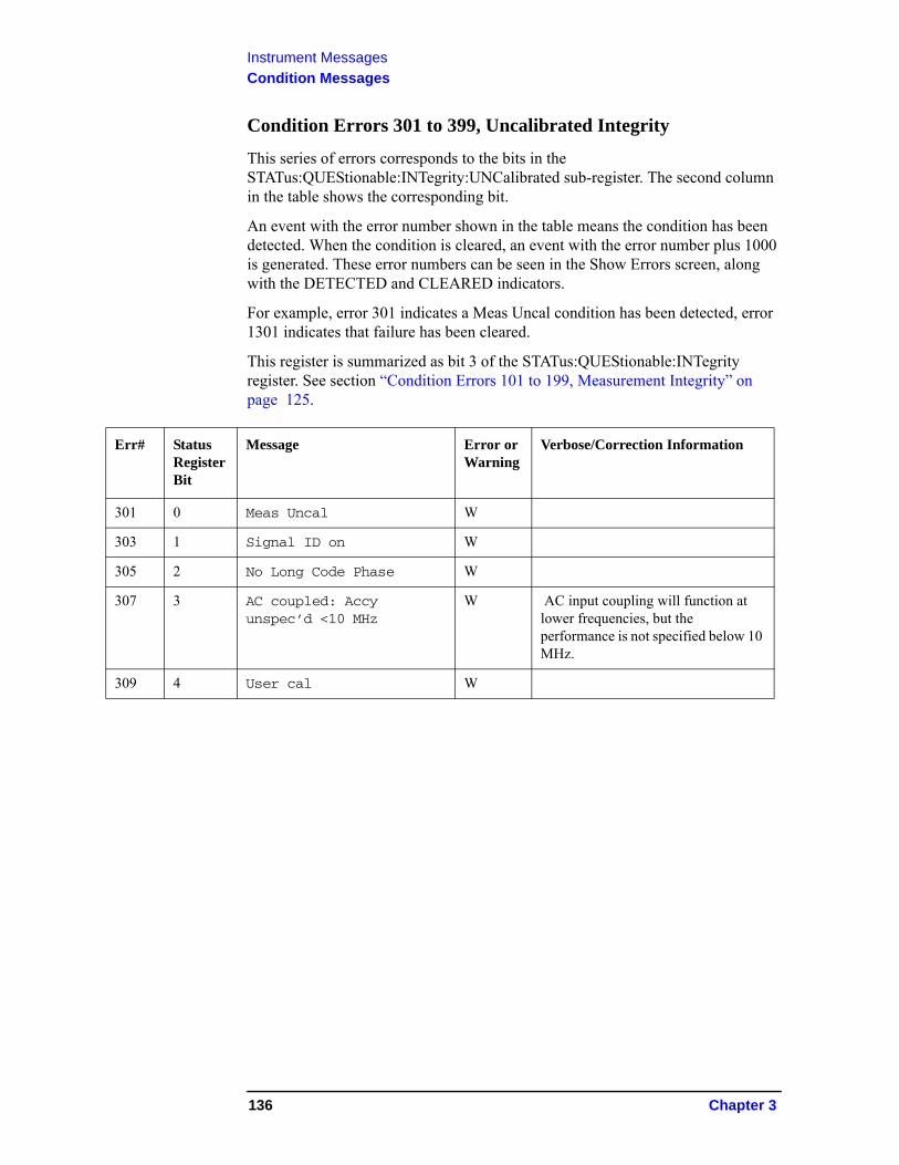
Instrument Messages
Condition Messages
Condition Errors 301 to 399, Uncalibrated Integrity
This series of errors corresponds to the bits in the STATus:QUEStionable:INTegrity:UNCalibrated sub-register. The second column in the table shows the corresponding bit.
An event with the error number shown in the table means the condition has been detected. When the condition is cleared, an event with the error number plus 1000 is generated. These error numbers can be seen in the Show Errors screen, along with the DETECTED and CLEARED indicators.
For example, error 301 indicates a Meas Uncal condition has been detected, error 1301 indicates that failure has been cleared.
This register is summarized as bit 3 of the STATus:QUEStionable:INTegrity register. See section “Condition Errors 101 to 199, Measurement Integrity” on page 125.
Err# Status Register Bit
Message Error or Warning
Verbose/Correction Information
301 0 Meas Uncal W
303 1 Signal ID on W
305 2 No Long Code Phase W
307 3 AC coupled: Accy unspec’d <10 MHz
W AC input coupling will function at lower frequencies, but the performance is not specified below 10 MHz.
309 4 User cal W
136 Chapter 3
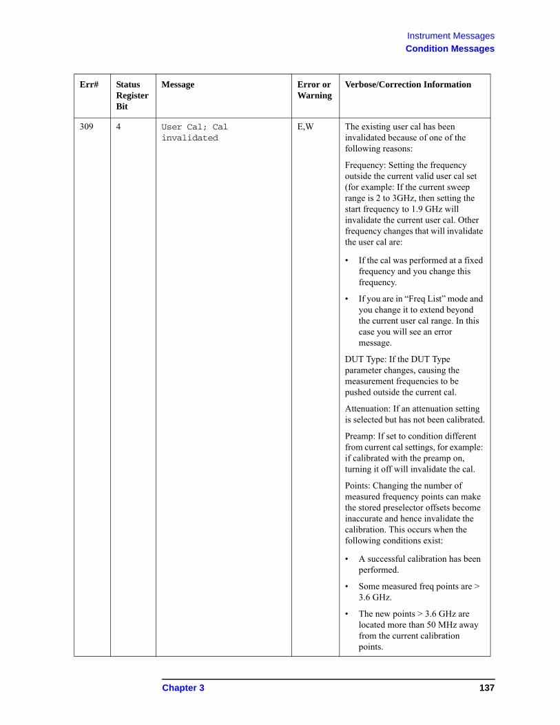
Instrument Messages
Condition Messages
309 4 User Cal; Cal invalidated
E,W The existing user cal has been invalidated because of one of the following reasons:
Frequency: Setting the frequency outside the current valid user cal set (for example: If the current sweep range is 2 to 3GHz, then setting the start frequency to 1.9 GHz will invalidate the current user cal. Other frequency changes that will invalidate the user cal are:
• If the cal was performed at a fixed frequency and you change this frequency.
• If you are in “Freq List” mode and you change it to extend beyond the current user cal range. In this case you will see an error message.
DUT Type: If the DUT Type parameter changes, causing the measurement frequencies to be pushed outside the current cal.
Attenuation: If an attenuation setting is selected but has not been calibrated.
Preamp: If set to condition different from current cal settings, for example: if calibrated with the preamp on, turning it off will invalidate the cal.
Points: Changing the number of measured frequency points can make the stored preselector offsets become inaccurate and hence invalidate the calibration. This occurs when the following conditions exist:
• A successful calibration has been performed.
• Some measured freq points are > 3.6 GHz.
• The new points > 3.6 GHz are located more than 50 MHz away from the current calibration points.
Err# Status Register Bit
Message Error or Warning
Verbose/Correction Information
Chapter 3 137
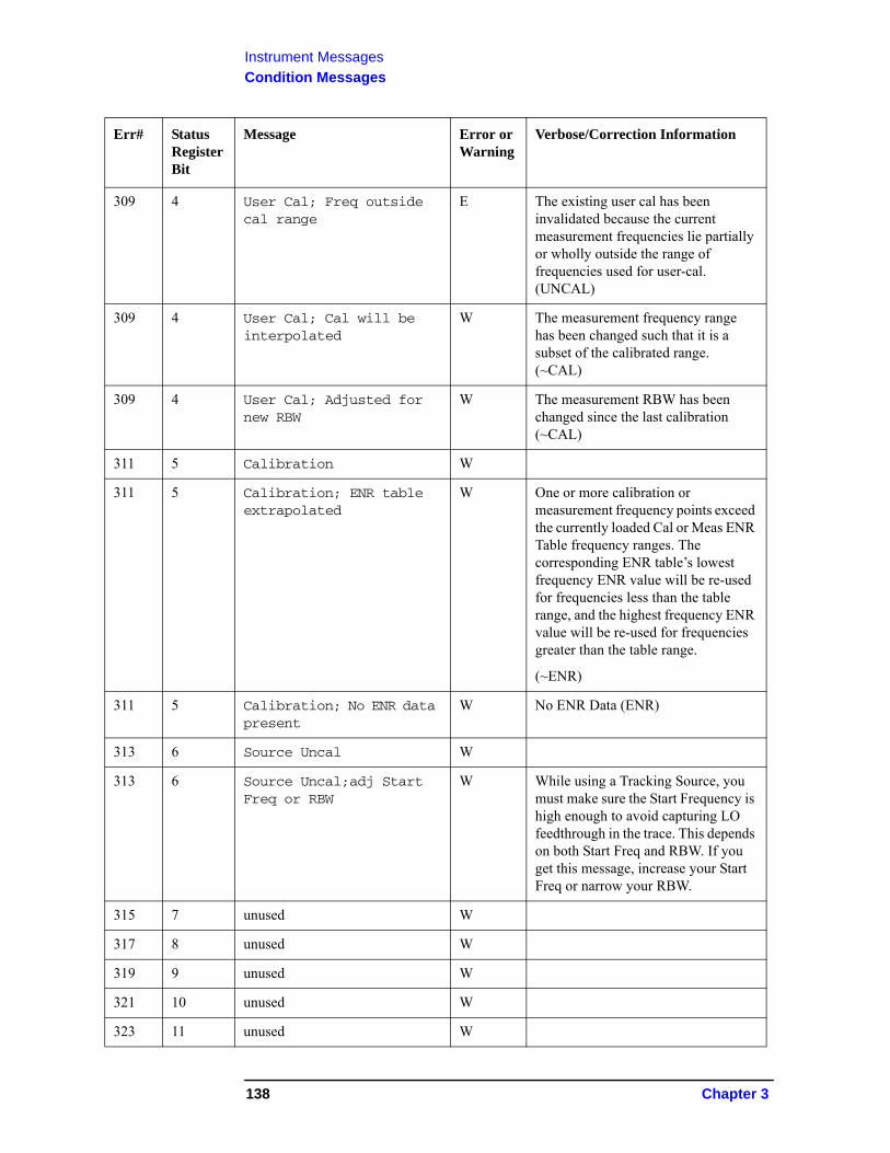
Instrument Messages
Condition Messages
309 4 User Cal; Freq outside cal range
E The existing user cal has been invalidated because the current measurement frequencies lie partially or wholly outside the range of frequencies used for user-cal. (UNCAL)
309 4 User Cal; Cal will be interpolated
W The measurement frequency range has been changed such that it is a subset of the calibrated range. (~CAL)
309 4 User Cal; Adjusted for new RBW
W The measurement RBW has been changed since the last calibration (~CAL)
311 5 Calibration W
311 5 Calibration; ENR table extrapolated
W One or more calibration or measurement frequency points exceed the currently loaded Cal or Meas ENR Table frequency ranges. The corresponding ENR table’s lowest frequency ENR value will be re-used for frequencies less than the table range, and the highest frequency ENR value will be re-used for frequencies greater than the table range.
(~ENR)
311 5 Calibration; No ENR data present
W No ENR Data (ENR)
313 6 Source Uncal W
313 6 Source Uncal;adj Start Freq or RBW
W While using a Tracking Source, you must make sure the Start Frequency is high enough to avoid capturing LO feedthrough in the trace. This depends on both Start Freq and RBW. If you get this message, increase your Start Freq or narrow your RBW.
315 7 unused W
317 8 unused W
319 9 unused W
321 10 unused W
323 11 unused W
Err# Status Register Bit
Message Error or Warning
Verbose/Correction Information
138 Chapter 3
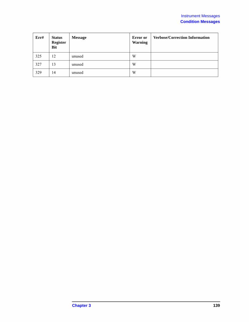
Instrument Messages
Condition Messages
325 12 unused W
327 13 unused W
329 14 unused W
Err# Status Register Bit
Message Error or Warning
Verbose/Correction Information
Chapter 3 139
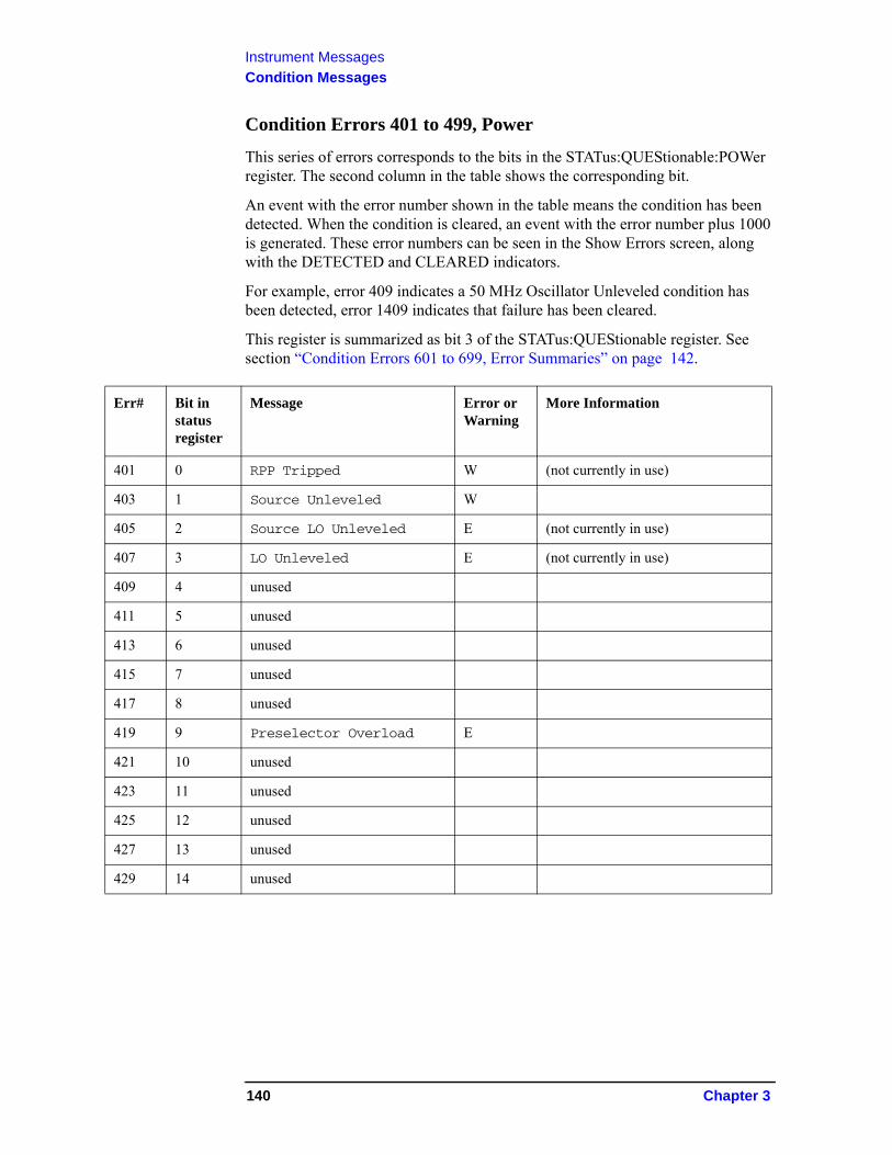
Instrument Messages
Condition Messages
Condition Errors 401 to 499, Power
This series of errors corresponds to the bits in the STATus:QUEStionable:POWer register. The second column in the table shows the corresponding bit.
An event with the error number shown in the table means the condition has been detected. When the condition is cleared, an event with the error number plus 1000 is generated. These error numbers can be seen in the Show Errors screen, along with the DETECTED and CLEARED indicators.
For example, error 409 indicates a 50 MHz Oscillator Unleveled condition has been detected, error 1409 indicates that failure has been cleared.
This register is summarized as bit 3 of the STATus:QUEStionable register. See section “Condition Errors 601 to 699, Error Summaries” on page 142.
Err# Bit in status register
Message Error or Warning
More Information
401 0 RPP Tripped W (not currently in use)
403 1 Source Unleveled W
405 2 Source LO Unleveled E (not currently in use)
407 3 LO Unleveled E (not currently in use)
409 4 unused
411 5 unused
413 6 unused
415 7 unused
417 8 unused
419 9 Preselector Overload E
421 10 unused
423 11 unused
425 12 unused
427 13 unused
429 14 unused
140 Chapter 3
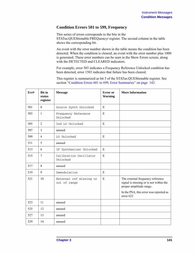
Instrument Messages
Condition Messages
Condition Errors 501 to 599, Frequency
This series of errors corresponds to the bits in the STATus:QUEStionable:FREQuencyr register. The second column in the table shows the corresponding bit.
An event with the error number shown in the table means the condition has been detected. When the condition is cleared, an event with the error number plus 1000 is generated. These error numbers can be seen in the Show Errors screen, along with the DETECTED and CLEARED indicators.
For example, error 503 indicates a Frequency Reference Unlocked condition has been detected, error 1503 indicates that failure has been cleared.
This register is summarized as bit 5 of the STATus:QUEStionable register. See section “Condition Errors 601 to 699, Error Summaries” on page 142.
Err# Bit in status register
Message Error or Warning
More Information
501 0 Source Synth Unlocked E
503 1 Frequency Reference Unlocked
E
505 2 2nd LO Unlocked E
507 3 unused
509 4 LO Unlocked E
511 5 unused
513 6 IF Synthesizer Unlocked E
515 7 Calibration Oscillator Unlocked
E
517 8 unused
519 9 Demodulation E
521 10 External ref missing or out of range
E The external frequency reference signal is missing or is not within the proper amplitude range.
In the PSA, this error was reported as error 622
523 11 unused
525 12 unused
527 13 unused
529 14 unused
Chapter 3 141
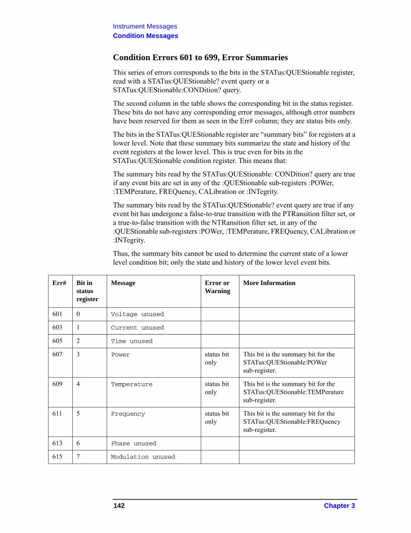
Instrument Messages
Condition Messages
Condition Errors 601 to 699, Error Summaries
This series of errors corresponds to the bits in the STATus:QUEStionable register, read with a STATus:QUEStionable? event query or a STATus:QUEStionable:CONDition? query.
The second column in the table shows the corresponding bit in the status register. These bits do not have any corresponding error messages, although error numbers have been reserved for them as seen in the Err# column; they are status bits only.
The bits in the STATus:QUEStionable register are “summary bits” for registers at a lower level. Note that these summary bits summarize the state and history of the event registers at the lower level. This is true even for bits in the STATus:QUEStionable condition register. This means that:
The summary bits read by the STATus:QUEStionable: CONDition? query are true if any event bits are set in any of the :QUEStionable sub-registers :POWer, :TEMPerature, FREQuency, CALibration or :INTegrity.
The summary bits read by the STATus:QUEStionable? event query are true if any event bit has undergone a false-to-true transition with the PTRansition filter set, or a true-to-false transition with the NTRansition filter set, in any of the :QUEStionable sub-registers :POWer, :TEMPerature, FREQuency, CALibration or :INTegrity.
Thus, the summary bits cannot be used to determine the current state of a lower level condition bit; only the state and history of the lower level event bits.
Err# Bit in status register
Message Error or Warning
More Information
601 0 Voltage unused
603 1 Current unused
605 2 Time unused
607 3 Power status bit only
This bit is the summary bit for the STATus:QUEStionable:POWer sub-register.
609 4 Temperature status bit only
This bit is the summary bit for the STATus:QUEStionable:TEMPerature sub-register.
611 5 Frequency status bit only
This bit is the summary bit for the STATus:QUEStionable:FREQuency sub-register.
613 6 Phase unused
615 7 Modulation unused
142 Chapter 3
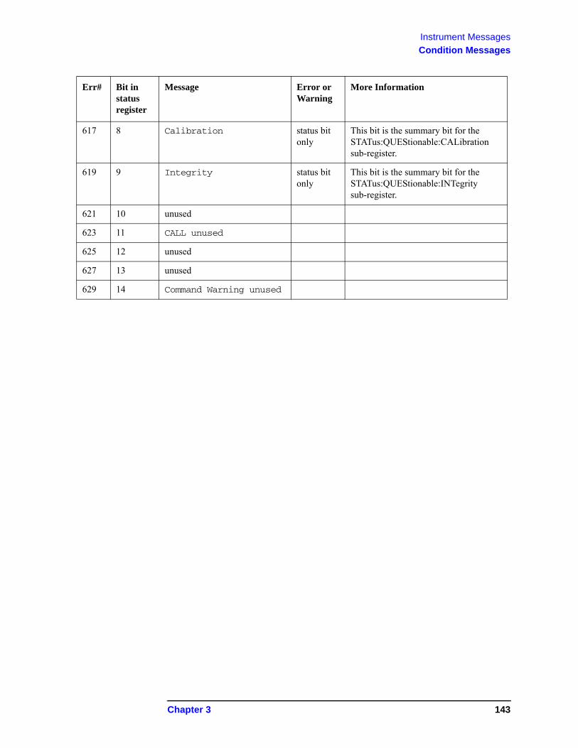
Instrument Messages
Condition Messages
617 8 Calibration status bit only
This bit is the summary bit for the STATus:QUEStionable:CALibration sub-register.
619 9 Integrity status bit only
This bit is the summary bit for the STATus:QUEStionable:INTegrity sub-register.
621 10 unused
623 11 CALL unused
625 12 unused
627 13 unused
629 14 Command Warning unused
Err# Bit in status register
Message Error or Warning
More Information
Chapter 3 143
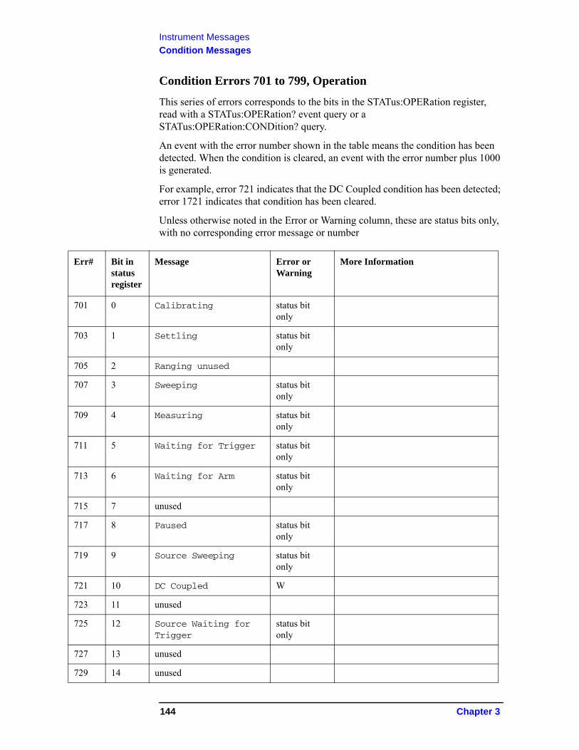
Instrument Messages
Condition Messages
Condition Errors 701 to 799, Operation
This series of errors corresponds to the bits in the STATus:OPERation register, read with a STATus:OPERation? event query or a STATus:OPERation:CONDition? query.
An event with the error number shown in the table means the condition has been detected. When the condition is cleared, an event with the error number plus 1000 is generated.
For example, error 721 indicates that the DC Coupled condition has been detected; error 1721 indicates that condition has been cleared.
Unless otherwise noted in the Error or Warning column, these are status bits only, with no corresponding error message or number
Err# Bit in status register
Message Error or Warning
More Information
701 0 Calibrating status bit only
703 1 Settling status bit only
705 2 Ranging unused
707 3 Sweeping status bit only
709 4 Measuring status bit only
711 5 Waiting for Trigger status bit only
713 6 Waiting for Arm status bit only
715 7 unused
717 8 Paused status bit only
719 9 Source Sweeping status bit only
721 10 DC Coupled W
723 11 unused
725 12 Source Waiting for Trigger
status bit only
727 13 unused
729 14 unused
144 Chapter 3
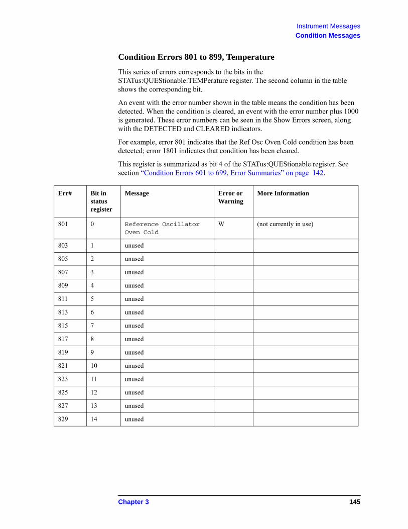
Instrument Messages
Condition Messages
Condition Errors 801 to 899, Temperature
This series of errors corresponds to the bits in the STATus:QUEStionable:TEMPerature register. The second column in the table shows the corresponding bit.
An event with the error number shown in the table means the condition has been detected. When the condition is cleared, an event with the error number plus 1000 is generated. These error numbers can be seen in the Show Errors screen, along with the DETECTED and CLEARED indicators.
For example, error 801 indicates that the Ref Osc Oven Cold condition has been detected; error 1801 indicates that condition has been cleared.
This register is summarized as bit 4 of the STATus:QUEStionable register. See section “Condition Errors 601 to 699, Error Summaries” on page 142.
Err# Bit in status register
Message Error or Warning
More Information
801 0 Reference Oscillator Oven Cold
W (not currently in use)
803 1 unused
805 2 unused
807 3 unused
809 4 unused
811 5 unused
813 6 unused
815 7 unused
817 8 unused
819 9 unused
821 10 unused
823 11 unused
825 12 unused
827 13 unused
829 14 unused
Chapter 3 145

Instrument Messages
Condition Messages
146 Chapter 3
4 RF Section Troubleshooting(RF/Microwave Analyzers)
147

RF Section Troubleshooting (RF/Microwave Analyzers)
What You Will Find in This Chapter
What You Will Find in This Chapter
The following information is found in this chapter:
1. Theory of operation of the RF section.2. Isolating the cause of an hardware problem by verifying the functionality of
assemblies in the RF section signal path.
NOTE Each section describes how the assembly works and gives information to help you troubleshoot the assembly. Each description covers the purpose of the assembly, describes the main components, and lists external connections to the assembly.
The following sections are found in this chapter:
RF Section Description on page 149
Quick Check to Verify the Low Band Signal Path on page 155
Troubleshooting a Low Band Problem on page 158
Quick Check to Verify High Band RF Path on page 163
Troubleshooting a High Band Problem on page 167
148 Chapter 4
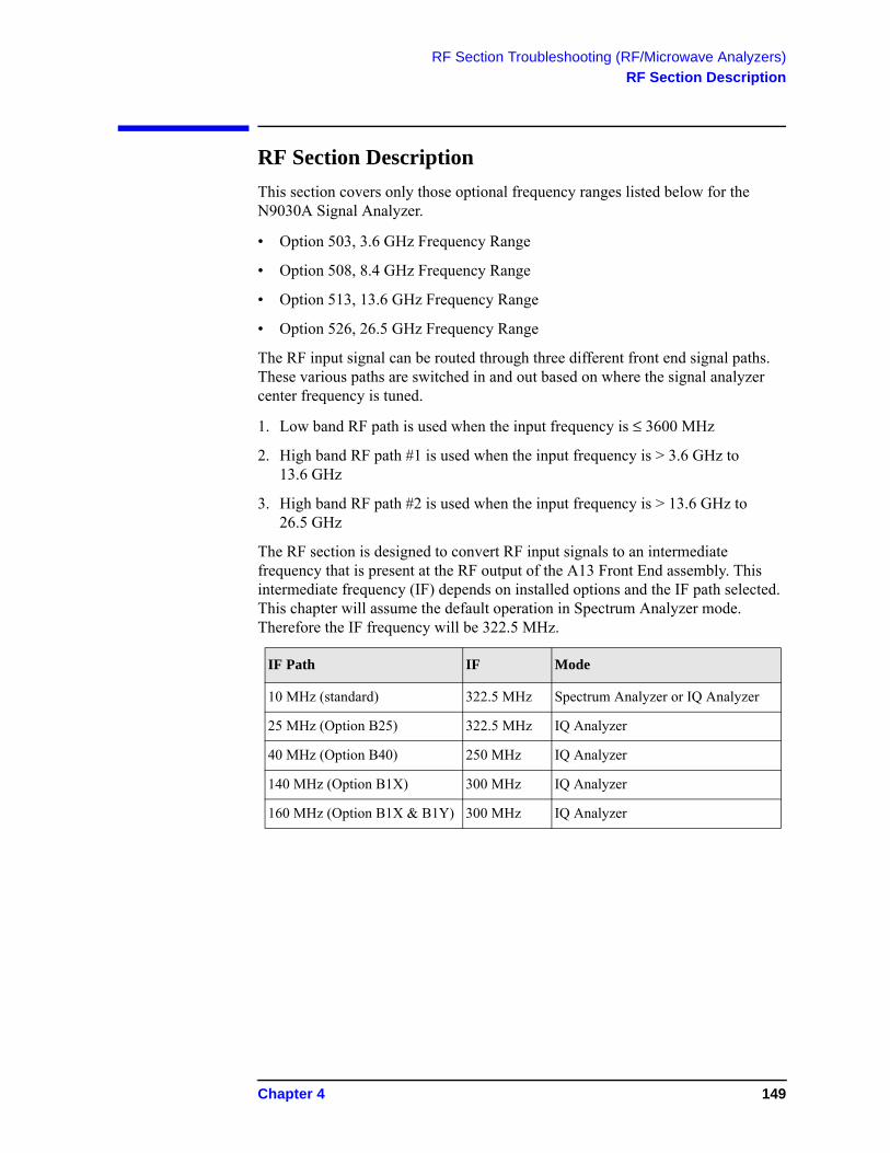
RF Section Troubleshooting (RF/Microwave Analyzers)
RF Section Description
RF Section Description
This section covers only those optional frequency ranges listed below for the N9030A Signal Analyzer.
• Option 503, 3.6 GHz Frequency Range
• Option 508, 8.4 GHz Frequency Range
• Option 513, 13.6 GHz Frequency Range
• Option 526, 26.5 GHz Frequency Range
The RF input signal can be routed through three different front end signal paths. These various paths are switched in and out based on where the signal analyzer center frequency is tuned.
1. Low band RF path is used when the input frequency is ≤ 3600 MHz
2. High band RF path #1 is used when the input frequency is > 3.6 GHz to 13.6 GHz
3. High band RF path #2 is used when the input frequency is > 13.6 GHz to 26.5 GHz
The RF section is designed to convert RF input signals to an intermediate frequency that is present at the RF output of the A13 Front End assembly. This intermediate frequency (IF) depends on installed options and the IF path selected. This chapter will assume the default operation in Spectrum Analyzer mode. Therefore the IF frequency will be 322.5 MHz.
IF Path IF Mode
10 MHz (standard) 322.5 MHz Spectrum Analyzer or IQ Analyzer
25 MHz (Option B25) 322.5 MHz IQ Analyzer
40 MHz (Option B40) 250 MHz IQ Analyzer
140 MHz (Option B1X) 300 MHz IQ Analyzer
160 MHz (Option B1X & B1Y) 300 MHz IQ Analyzer
Chapter 4 149
RF Section Troubleshooting (RF/Microwave Analyzers)
RF Section Description
The RF section is comprised of the following major assemblies:
• A9 Input Attenuator A
• A10 Input Attenuator B
• A11 Low Band Switch Assembly
• A12 YTF Preselector
• A20 Yig Tuned Oscillator
• A13 RF Front End Assembly - shown on the block diagram as A13A1 and A13A2, however the entire A13 assembly must be replaced.
• A15 Front End Control Assembly
• Option LNP - Low Noise Path
• Option MPB - Microwave Preselector Bypass
1. RF input frequencies < 3600 MHz route through the low band path. Refer to the RF Lowband Path Block Diagram in Chapter 13 for details.
The RF input signal level can be optimized by Input Attenuator A and/or Input Attenuator B. The low band switch assembly contains a limiter that offers added protection for the mixer, and routes the input signal to the low band input of the A13 RF Front End assembly. There are (3) different signal paths on the input of the RF Front End assembly that the signal can be routed through depending on installed options and front panel settings.
• Electronic Attenuator path, 0-24 dB (Option EA3)• Low Band Preamplifier path, 20 dB nominal gain (Option P03)• Direct to Mixer #1
NOTE The RF input signal can route through the Electronic Attenuator section or the Preamplifier, but not both. All RF input frequencies < 3600 MHz go to Mixer #1.
The RF input signal is then mixed with the 1st LO from the A20 YTO assembly
to a 1st intermediate frequency of 5122.5 MHz. Since the RF input signal is <3600 MHz for low band, this RF input signal is upconverted in Mixer #1 to
the 1st IF. This 1st IF signal is then downconverted in Mixer #2 using the
4800 MHz 2nd LO generated on the A16 Reference assembly to a 2nd
intermediate frequency of 322.5 MHz (5122.5 MHz (1st IF) − 4800 MHz
(2nd LO)). The 2nd IF output is at A13A1J7. This signal path is used for all frequency range options when the RF input frequencies are < 3600 MHz. The control voltages and biasing for these assemblies come from the A15 Front End Control assembly.
150 Chapter 4
RF Section Troubleshooting (RF/Microwave Analyzers)
RF Section Description
2. RF input frequencies from 3.6 GHz to 13.6 GHz go through the high band path. Refer to the RF Highband Path #1 Block Diagram in Chapter 13 for details.
The input signal level can be optimized by Input Attenuator A and/or Input Attenuator B. The Low Band Switch assembly routes the signal through the A12 YTF Preselector. If one of the optional high band preamps is licensed, the signal can be routed through the preamp. The A15 Front End Controller provides switching signals.
The Low Band Switch assembly performs the following tasks:
• Provides a limiter that offers added protection for the mixer and optional preamp.
• Contains the high band preamp.• Routes the input signal to the A12 YTF Preselector. If Options LNP or MPB
are installed, the signal is routed through switches.
The high band input switch in the Front End Assembly routes the RF input
signal to Mixer #2, where it mixes with the LO and provides a 1st intermediate frequency of 322.5 MHz. The 322.5 MHz IF output is at A13A1J7. This is the signal path for Option 508, 8.4 GHz Frequency Range, Option 513, 13.6 GHz Frequency Range, and Option 526, 26.5 GHz Frequency Range (up to 13.6 GHz). The control voltages and biasing are provided by the A15 Front End Control Assembly.
3. RF input frequencies from 13.6 GHz to 26.5 GHz go through the high band path. Refer to the RF Highband Path #2 Block Diagram in Chapter 13 for details.
The signal path for 13.6 GHz to 26.5 Ghz operation is almost the same as the 3.6 GHz to 13.6 GHz path. The only difference is that Mixer #3 is used in this path. The LO is doubled at tuned frequencies above 17 GHz.
A9 Input Attenuator A
This assembly has two 2 dB attenuator sections, a DC block and a cal signal input port. With the DC block switched in (AC coupled mode), the low end minimum frequency range increases from 3 Hz to 10 MHz due to capacitive effects.
A10 Input Attenuator B
This assembly has a total of 66 dB of attenuation to control the signal level into the Low Band Switch assembly. There is a 6 dB, 10 dB, 20 dB, and 30 dB section in the A10 assembly. Total input attenuation with the A9 and the A10 combined is 70 dB in 2 dB steps.
Chapter 4 151
RF Section Troubleshooting (RF/Microwave Analyzers)
RF Section Description
A11 Low Band Switch
This assembly operates across the entire frequency range of the analyzer. The switch has 3 main functions:
• Switch RF input frequencies from 3 Hz to 3.59 GHz RF Output to A13 RF Front End Assembly.
• Switch input frequencies from 3.6 GHz to 26.5 GHz Microwave RF Output to A12, YTF Preselector.
• Contains optional high band preamplifier, which has a typical gain of 30 dB and a noise figure from 9 to 12 dB up to 18 GHz.
A12 YTF Preselector
The YTF Preselector is used for input frequencies greater than 3.6 GHz. Signals less than 3.6 GHz bypass the YTF assembly and are routed to the low band input of the A13 RF Front End Assembly. The YTF Preselector is a YIG tunable bandpass filter whose main purpose is to track the input signal and to filter out unwanted spurious or image response signals. The YTF Preselector has a 3 dB bandwidth greater than 40 MHz and an insertion loss of ~ 6.5 dB.
The preselector requires centering for optimum amplitude accuracy. The Auto Align routine will perform a rough centering during the preselector two point tuning algorithm. However, when troubleshooting, press Amplitude, Preselector Center to manually center the preselector.
The YTF Preselector is not present in analyzers with Option 503, 3.6 GHz frequency range.
A20 YTO Assembly
Provides the 1st LO signal that is required for the A13 RF Front End Assembly.
The 1st LO has a frequency range from 3.80 to 8.73 GHz. The output power is +13 to +18 dBm. In order to maximize the conversion efficiency and avoid LO unlock, sufficient LO power must be supplied.
152 Chapter 4
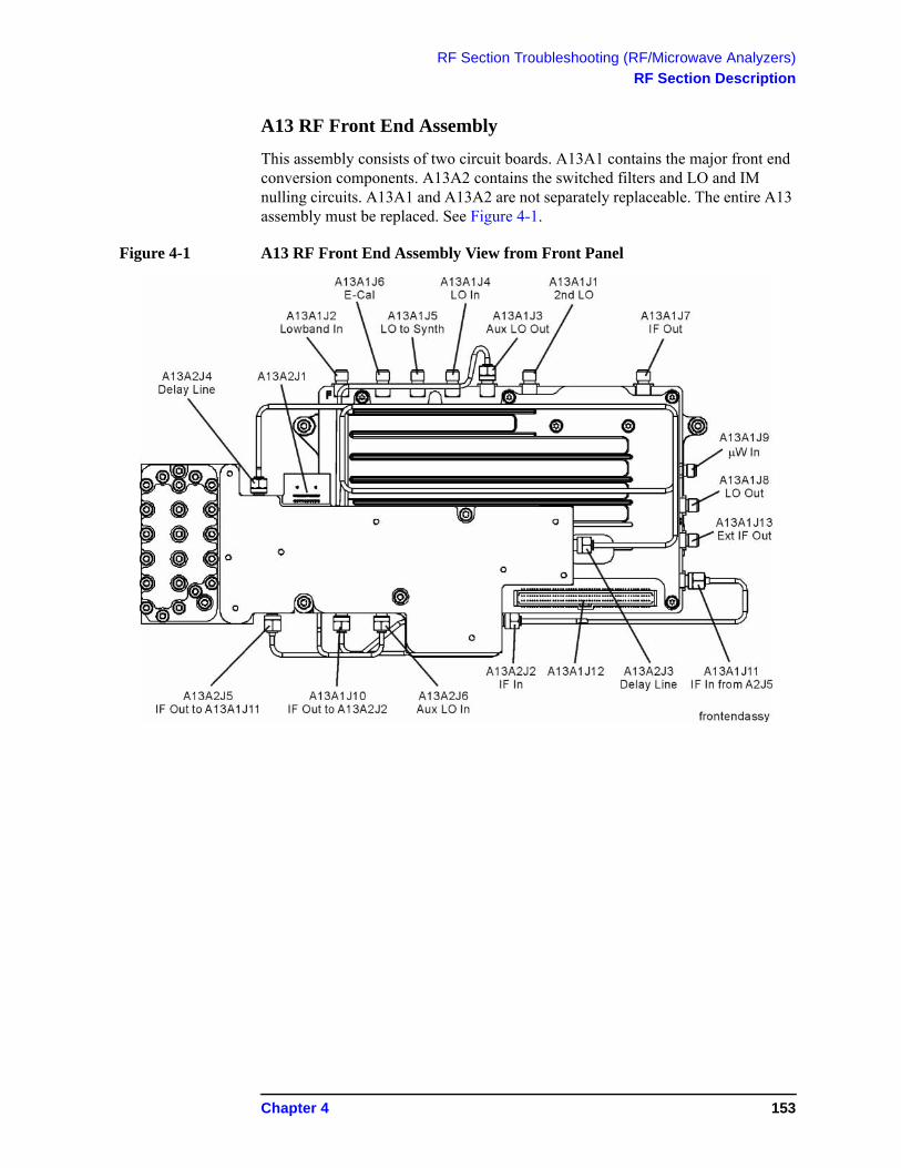
RF Section Troubleshooting (RF/Microwave Analyzers)
RF Section Description
A13 RF Front End Assembly
This assembly consists of two circuit boards. A13A1 contains the major front end conversion components. A13A2 contains the switched filters and LO and IM nulling circuits. A13A1 and A13A2 are not separately replaceable. The entire A13 assembly must be replaced. See Figure 4-1.
Figure 4-1 A13 RF Front End Assembly View from Front Panel
Chapter 4 153
RF Section Troubleshooting (RF/Microwave Analyzers)
RF Section Description
This assembly contains the following circuits:
• Input Low-pass filter (RF input signals < 3.6 GHz)
• Optional Low Band Electronic Attenuator (0-24 dB attenuation control)
• Optional Low Band Preamplifier and Limiter
• RF Mixer #1 (RF input signals < 3.6 GHz)
• 1st LO Sub-system (3.8 GHz to 8.7 GHz)
• 1st IF Amplifier (5122.5 MHz)
• Switched Filters (A13A2) provides wide BW band pass filter (low band)
• LO and IM nulling (A13A2)
• Mixer #2 (RF input signals 3.6 GHz to 13.599 GHz)
• Microwave Input Amplifier
• Mixer #3 (RF input signals 13.6 GHz to 26.5 GHz)
• LO Doubler
• External Mixing Diplexer
A15 Front End Control Assembly
Provides the correct biasing and switch control logic to the following RF assemblies:
• Input Attenuator A
• Input Attenuator B
• Low Band Switch
• (Option LNP) Low Noise Path
• YTF Preselector (Input signals > 3.6 GHz)
• (Option MPB) Microwave Preselector Bypass
• Front End Assembly including switched filter
• (Optional) High Band Preamplifier
• (Optional) Low Band Preamplifier
• (Option EA3) Electronic Attenuator (0-24 dB)
NOTE Refer to Chapter 6 , “Front End Control Troubleshooting” for detailed descriptions & troubleshooting procedures
154 Chapter 4
RF Section Troubleshooting (RF/Microwave Analyzers)
Troubleshooting
Troubleshooting
Quick Check to Verify the Low Band Signal Path
The analyzer has an internal 50 MHz amplitude reference signal that is used to verify the low band path. This 50 MHz calibrator is used when the analyzer performs many of the internal alignment routines. Therefore, the functionality of the 50 MHz calibrator and low band path are critical to passing Align All Now. Refer to the RF Lowband Path Block Diagram (Options 503, 508, 513, and 526) in Chapter 13 for details. Reference the instrument settings box on the block diagram.
Equipment needed:
Spectrum Analyzer with frequency range to 8 GHz
Signal source with output power 0 dBm and frequency range to at least 3.6 GHz
Power splitter, 11667B
2 each, quality SMA or 3.5 mm cables
90° SMA (m) to SMA (f) adapter
MMCX (f) to SMA (f) cable
SMA (f) to SMA (f) adapter
SMA (m) to SMA (m) adapter
NOTE To perform the following checks, it will be necessary to remove the outer cover and the top brace. See Chapter 16 for removal procedures.
Turn the instrument on and allow it to complete its full boot up process to Spectrum Analyzer mode. Use the internal 50 MHz, −25 dBm calibrator signal as a reference for troubleshooting by pressing Mode Preset, Input/Output, RF Calibrator, 50 MHz on the analyzer. Now press FREQ (Channel), 50 MHz, SPAN (X Scale), 1 MHz, Peak Search. The 50 MHz reference signal should measure 50 MHz @ −25 dBm ± 2 dB on the analyzer display. If the power level is within tolerance, the low band path is functioning correctly at 50 MHz. If the power level is incorrect, select the 4.8 GHz RF Calibrator and set the analyzer center frequency to 4.8 GHz. Since several of the same signal path components are shared between low band and high band, determining if the problem appears in both paths is helpful.
To verify the high band path go to “Quick Check to Verify High Band RF Path” on page 163.
If the power level is not within tolerance, press SPAN (X Scale), Zero Span, AMPTD (Y Scale), Attenuation, 10 dB.
Chapter 4 155
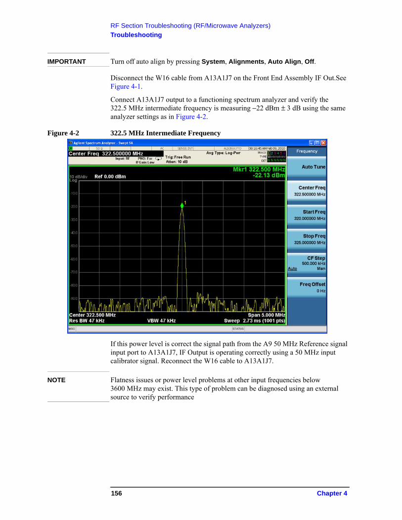
RF Section Troubleshooting (RF/Microwave Analyzers)
Troubleshooting
IMPORTANT Turn off auto align by pressing System, Alignments, Auto Align, Off.
Disconnect the W16 cable from A13A1J7 on the Front End Assembly IF Out.See Figure 4-1.
Connect A13A1J7 output to a functioning spectrum analyzer and verify the 322.5 MHz intermediate frequency is measuring −22 dBm ± 3 dB using the same analyzer settings as in Figure 4-2.
Figure 4-2 322.5 MHz Intermediate Frequency
If this power level is correct the signal path from the A9 50 MHz Reference signal input port to A13A1J7, IF Output is operating correctly using a 50 MHz input calibrator signal. Reconnect the W16 cable to A13A1J7.
NOTE Flatness issues or power level problems at other input frequencies below 3600 MHz may exist. This type of problem can be diagnosed using an external source to verify performance
156 Chapter 4
RF Section Troubleshooting (RF/Microwave Analyzers)
Troubleshooting
If this power level is incorrect, the following assemblies need to be verified using the 50 MHz internal calibrator signal. Be sure the 50 MHz calibrator is turned on. Press Input/Output, RF Calibrator, 50 MHz when verifying the performance.
1. A11 Low Band Switch
2. A10 Input Attenuator B
3. A9 Input Attenuator A
4. A16 Reference Assembly (50 MHz calibrator, 2nd LO)
5. A20 YTO
6. A13 RF Front End Assembly
NOTE In order to gain access to the front end components, remove the front frame assembly, but leave the ribbon cable connected so you can still control the instrument. Remove the right side chassis. Refer to the removal procedures in Chapter 16, “Assembly Replacement Procedures”.
Chapter 4 157
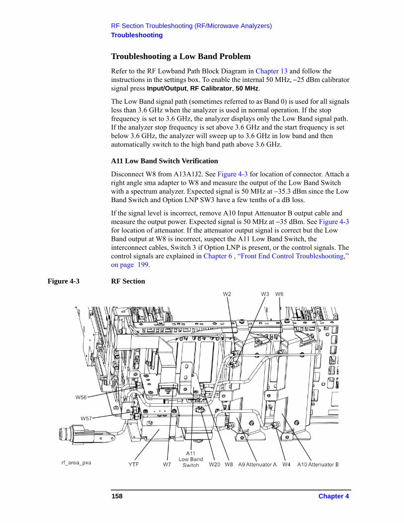
RF Section Troubleshooting (RF/Microwave Analyzers)
Troubleshooting
Troubleshooting a Low Band Problem
Refer to the RF Lowband Path Block Diagram in Chapter 13 and follow the instructions in the settings box. To enable the internal 50 MHz, −25 dBm calibrator signal press Input/Output, RF Calibrator, 50 MHz.
The Low Band signal path (sometimes referred to as Band 0) is used for all signals less than 3.6 GHz when the analyzer is used in normal operation. If the stop frequency is set to 3.6 GHz, the analyzer displays only the Low Band signal path. If the analyzer stop frequency is set above 3.6 GHz and the start frequency is set below 3.6 GHz, the analyzer will sweep up to 3.6 GHz in low band and then automatically switch to the high band path above 3.6 GHz.
A11 Low Band Switch Verification
Disconnect W8 from A13A1J2. See Figure 4-3 for location of connector. Attach a right angle sma adapter to W8 and measure the output of the Low Band Switch with a spectrum analyzer. Expected signal is 50 MHz at −35.3 dBm since the Low Band Switch and Option LNP SW3 have a few tenths of a dB loss.
If the signal level is incorrect, remove A10 Input Attenuator B output cable and measure the output power. Expected signal is 50 MHz at −35 dBm. See Figure 4-3 for location of attenuator. If the attenuator output signal is correct but the Low Band output at W8 is incorrect, suspect the A11 Low Band Switch, the interconnect cables, Switch 3 if Option LNP is present, or the control signals. The control signals are explained in Chapter 6 , “Front End Control Troubleshooting,” on page 199.
Figure 4-3 RF Section
158 Chapter 4
RF Section Troubleshooting (RF/Microwave Analyzers)
Troubleshooting
A9 Input Attenuator and A10 Input Attenuator Verification
Calibrator Switch Test
On the A16 Reference assembly, disconnect semi rigid cable W3 from A16J701 and measure A16J701 with a spectrum analyzer. Expected signal is 50 MHz at −25 dBm ± 0.5 dB. If signal level is incorrect, suspect A16 Reference assembly is faulty, or the 50 MHz calibrator amplitude requires adjustment using the field calibration software.
To verify calibrator switch operation, connect external signal source set to 50 MHz and −25 dBm to the RF input connector of analyzer under test. Press Input/Output, RF Calibrator, Off. If the signal level at the attenuator output is now correct, suspect the A9 Attenuator cal switch or a faulty control signal from the A15 Front End Controller assembly.
Attenuator Check
Set the signal source connected to the analyzer input port to 0 dBm. On the analyzer, press Amplitude, Attenuation, and change input attenuation to 0 dB. The measuring spectrum analyzer connected to A10 Attenuator output port should indicate a 0 dBm level.
Change the input attenuation on the analyzer under test to 2 dB. See the chart below for expected measurement values at the A10 Attenuator output port.
Analyzer Under TestAttenuator Setting (dB)
Power at A10 Output Port
Input Attenuator Being Tested
0 0 dBm (reference) Both set to through path
2 −2 A9
4 −4 A9
6 −6 A10
8 −8 A9 set to 2 dB, A10 set to 6 dB
10 −10 A10
20 −20 A10
30 −30 A10
40 −40 A10
50 −50 A10
60 −60 A10
70 −70 A9 set to 4 dB, A10 set to 66 dB
Chapter 4 159
RF Section Troubleshooting (RF/Microwave Analyzers)
Troubleshooting
Second LO Level Verification
The second LO signal comes from the A16 Reference Assembly and is only used in Low Band. The second LO signal can be measured on the Front End Assembly at A13A1J1 or the A16 Reference Assembly at A16J702. Expected signal is 4800 MHz at +10 dBm when a low loss test cable is used and with the measuring spectrum analyzer input attenuator set to at least 20 dB to prevent overload.
First LO Level Verification
The first LO is the A20 YTO assembly. The first LO is phased locked by the A14 Synthesizer assembly and controlled by tuning signals from the A15 Front End Controller.
To assure the first LO is tuned to the correct frequency and power, measure the A13 Front End assembly at A13A1J3 when the analyzer center frequency is 50 MHz. This test port is chosen because removing cable W19 will not cause the analyzer LO phase lock loop to unlock, which would affect the LO frequency measurement.
The LO signal should measure 5172.5 MHz at +10 dBm ± 3 dB.
If the signal level is incorrect, measure the signal coming from the A20 YTO at A13A1J4. In order to measure this signal and avoid an LO Unlock, you will need to install a power splitter at A13A1J4. Connect one arm of the splitter to A13A1J4 using a sma (m) to sma (m) adapter. Connect the input of the splitter to W20 using the sma 90 degree adapter and short sma cable. Connect the measuring spectrum analyzer to the other arm of the splitter. Add the loss through the splitter arm which is 6 dB for the Agilent 11667B splitter.
The signal should be 5172.5 MHz at +10 dBm ± 3 dB
When measuring A13A1J5, Synth Out, the splitter must also be used. The expected signal level is 5172.5 MHz at +10 dBm ± 3 dB
A13 Front End Assembly Verification
NOTE The A13 Front End assembly is shown as A13A1 and A13A2 for troubleshooting clarification. However, A13A1 and A13A2 are not separately replaceable. The entire A13 assembly must be replaced.
Many portions of the Front End Assembly have been verified earlier in the Low Band troubleshooting process outlined above.
The input signal level was measured on W8 as part of the A11 Low Band Switch verification.
The output signal level was measured at A13A1J7 during the quick check to verify the Low Band Signal Path.
The Second LO input was tested during the Second LO Verification.
The LO input at W20, and the LO outputs were tested when performing the First LO Verification.
160 Chapter 4

RF Section Troubleshooting (RF/Microwave Analyzers)
Troubleshooting
It is possible to measure the W48 input cable to the Switched Filter where it connects to A13A2J2, and the output of the Switched Filter at W49 where it connects to A13A1J11. The A13A2 Switched Filter is not separately replaceable, but being able to determine where the signal level is faulty, can aid in verifying the faulty assembly. See the block diagram for signal levels
CAUTION When measuring W48, the analyzer must be powered down and ribbon cable W28 on the Switched Filter removed to gain access to W48. Once the measuring spectrum analyzer is connected to W48, the W28 ribbon cable must be reinstalled, and only then can the analyzer be powered back up. The ribbon cable is fragile so it cannot be bent out of the way to access the cable, and should not be removed and installed with power applied.
Electronic Attenuator Test (Option EA3)
The electronic attenuator is aligned as part of the System Gain internal alignment process. See the description of the initial alignments and the location of the alignment history file in the Boot Up and Initialization Troubleshooting chapter. Viewing the Alignment History file will tell you if other alignment tests failed, and reveal which electronic attenuator steps failed.
To verify the electronic attenuator operation on instruments with Option EA3, set up the analyzer to view the 50 MHz calibrator signal on screen. Press Input/Output, RF Calibrator, 50 MHz, Center Frequency, 50 MHz, Span, 500 kHz
Press Peak Search to place a marker on the calibrator signal, then press Marker Delta
Activate the electronic attenuator. Press AMPTD, Attenuation, Enable Elec Atten. Then press Elec Atten.
Press the up arrow key to step through all attenuator steps while monitoring the marker delta readout. The signal level should not change more than 0.4 dB as indicated by the marker delta readout.
If the attenuator switches slowly, or the signal is not present when the electronic attenuator is switched into the signal path or the signal appears only when the attenuator is switched on, suspect the control signals from the A15 Front End Controller are faulty or the A13 Front End assembly is faulty. If the attenuator switches, but the switching error between attenuator settings is greater than ± 0.4 dB, assure that any other internal alignment failures are resolved since the System Gain alignment must run before optimum performance is possible. Assure you have evaluated all causes before you replace the Front End assembly.
If you determine the problem is at a frequency other than 50 MHz, perform the low band flatness adjustment before replacing the Front End assembly.
Chapter 4 161
RF Section Troubleshooting (RF/Microwave Analyzers)
Troubleshooting
Low Band Preamp (Option P03, P08, P13, P26)
The Preamp is aligned as part of the System Gain internal alignment process. See the description of the initial alignments and the location of the alignment history file in Chapter 2, “Boot Up and Initialization Troubleshooting,” on page 47. Viewing the Alignment History file will tell you if other alignment tests failed, and reveal pass or fail information for the preamp.
If any of the preamp options are installed, the Low Band preamp can be verified as follows:
Set up the analyzer to view the 50 MHz calibrator signal on screen
Press AMPTD, Attenuation, and verify that the Enable Elec Atten key is set to Off. It is not possible to turn on both the electronic attenuator and preamp at the same time.
Press AMPTD, More, Internal Preamp, Low Band to activate the preamp.
The expected operation is the signal level will not change more than ± 0.5 dB and the noise floor will increase due to the fact the input attenuator is automatically increased. If the amplitude error when switching the preamp on and off is greater than 0.5 dB, assure that any other internal alignment failures are resolved since the System Gain alignment must run before optimum performance is possible. Assure you have evaluated all causes including A15 Front End Controller switching problems, before you replace the Front End assembly.
If you determine the problem is at a frequency other than 50 MHz, perform the low band flatness adjustment before replacing the Front End assembly.
Low Band Mixing Equations
Low Band first mixer:
RF = LO − IFIF = LO − RFLO = IF + RF
where RF is the input signal at the signal analyzer
Low Band second mixer:
RF = LO + IFIF = RF − LOLO = RF − IF
where RF in this case is the first IF signal (signal at A13A1J11)
162 Chapter 4
RF Section Troubleshooting (RF/Microwave Analyzers)
Troubleshooting
Quick Check to Verify High Band RF Path
Refer to the RF Highband Path #1 Block Diagram in Chapter 13 .
The High Band signal path (sometimes referred to as Band 1-Band 4) is used for all signals 3.6 GHz and above. If the start frequency is set to 3.6 GHz and above, the analyzer displays only the High Band signal path. If the analyzer start frequency is below 3.6 GHz and the Stop frequency is set above 3.6 GHz, the analyzer will start sweeping in Low Band up to 3.6 GHz, and then automatically switch to the high band path above 3.6 GHz.
Equipment needed:
Spectrum Analyzer with frequency range to 14 GHz
Signal source with output power 0 dBm and frequency range to at least 26 GHz
Power splitter, 11667B
2 each, quality SMA or 3.5 mm cables
90° SMA (m) to SMA (f) adapter
MMCX (f) to SMA (f) cable
SMA (f) to SMA (f) adapter
SMA (m) to SMA (m) adapter
NOTE To perform the following checks, it will be necessary to remove the outer cover and the top brace. See Chapter 16 for removal procedures.
Turn the instrument on and allow it to complete its full boot up process to Signal Analyzer mode. Use the internal 4.8 GHz, −28 dBm calibrator signal as a reference for troubleshooting by pressing Mode Preset, Input/Output, RF Calibrator, 4.8 GHz on the analyzer. Now press FREQ (Channel), 4.8 GHz, SPAN (X Scale), 1 MHz, Peak Search).
The 4.8 GHz reference signal should measure −28 dBm ± 2 dB on the analyzer display. If the power level is within tolerance, the 3.6 GHz to 13.6 Ghz path is functioning correctly at 4.8 Ghz.
If the power level is incorrect, select the 50 MHz RF calibrator and set the analyzer center frequency to 50 MHz. Since several of the same signal path components are shared between high band and low band, determining if the problem appears in both paths is helpful
IMPORTANT Turn off auto align by pressing System, Alignments, Auto Align, Off.
Chapter 4 163
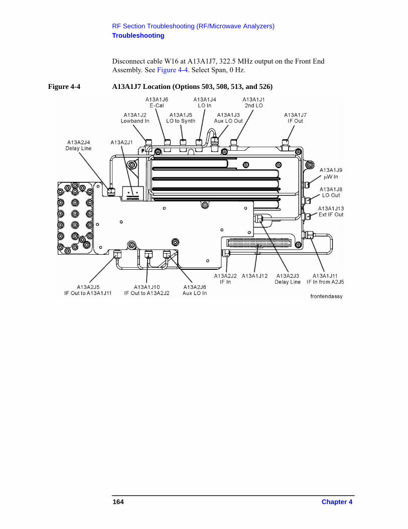
RF Section Troubleshooting (RF/Microwave Analyzers)
Troubleshooting
Disconnect cable W16 at A13A1J7, 322.5 MHz output on the Front End Assembly. See Figure 4-4. Select Span, 0 Hz.
Figure 4-4 A13A1J7 Location (Options 503, 508, 513, and 526)
164 Chapter 4
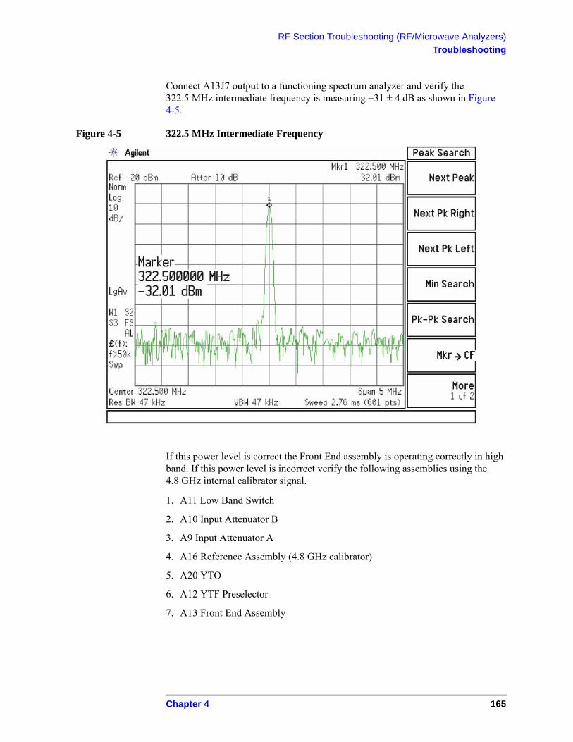
RF Section Troubleshooting (RF/Microwave Analyzers)
Troubleshooting
Connect A13J7 output to a functioning spectrum analyzer and verify the 322.5 MHz intermediate frequency is measuring −31 ± 4 dB as shown in Figure 4-5.
Figure 4-5 322.5 MHz Intermediate Frequency
If this power level is correct the Front End assembly is operating correctly in high band. If this power level is incorrect verify the following assemblies using the 4.8 GHz internal calibrator signal.
1. A11 Low Band Switch
2. A10 Input Attenuator B
3. A9 Input Attenuator A
4. A16 Reference Assembly (4.8 GHz calibrator)
5. A20 YTO
6. A12 YTF Preselector
7. A13 Front End Assembly
Chapter 4 165
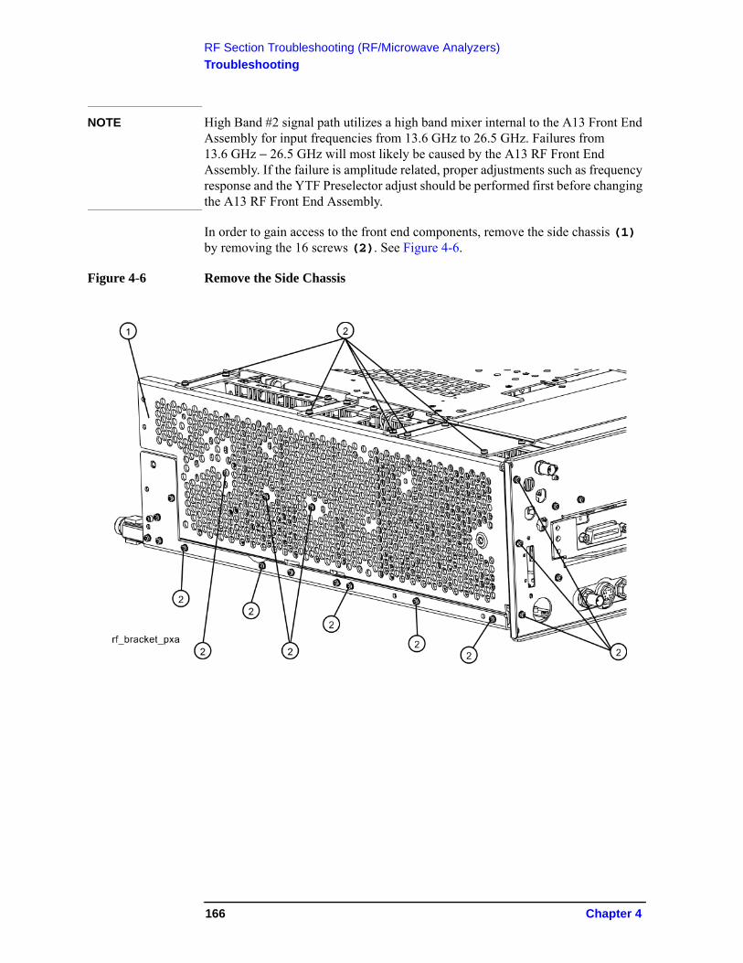
RF Section Troubleshooting (RF/Microwave Analyzers)
Troubleshooting
NOTE High Band #2 signal path utilizes a high band mixer internal to the A13 Front End Assembly for input frequencies from 13.6 GHz to 26.5 GHz. Failures from 13.6 GHz − 26.5 GHz will most likely be caused by the A13 RF Front End Assembly. If the failure is amplitude related, proper adjustments such as frequency response and the YTF Preselector adjust should be performed first before changing the A13 RF Front End Assembly.
In order to gain access to the front end components, remove the side chassis (1) by removing the 16 screws (2). See Figure 4-6.
Figure 4-6 Remove the Side Chassis
166 Chapter 4
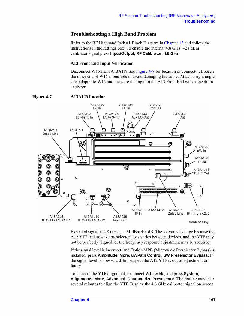
RF Section Troubleshooting (RF/Microwave Analyzers)
Troubleshooting
Troubleshooting a High Band Problem
Refer to the RF Highband Path #1 Block Diagram in Chapter 13 and follow the instructions in the settings box. To enable the internal 4.8 GHz, −28 dBm calibrator signal press Input/Output, RF Calibrator, 4.8 GHz.
A13 Front End Input Verification
Disconnect W15 from A13A1J9 See Figure 4-7 for location of connector. Loosen the other end of W15 if possible to avoid damaging the cable. Attach a right angle sma adapter to W15 and measure the input to the A13 Front End with a spectrum analyzer.
Figure 4-7 A13A1J9 Location
Expected signal is 4.8 GHz at −51 dBm ± 4 dB. The tolerance is large because the A12 YTF (microwave preselector) loss varies between devices, and the YTF may not be perfectly aligned, or the frequency response adjustment may be required.
If the signal level is incorrect, and Option MPB (Microwave Preselector Bypass) is installed, press Amplitude, More, uWPath Control, uW Preselector Bypass. If the signal level is now −52 dBm, suspect the A12 YTF is out of adjustment or faulty.
To perform the YTF alignment, reconnect W15 cable, and press System, Alignments, More, Advanced, Characterize Preselector. The routine may take several minutes to align the YTF. Display the 4.8 GHz calibrator signal on screen
Chapter 4 167
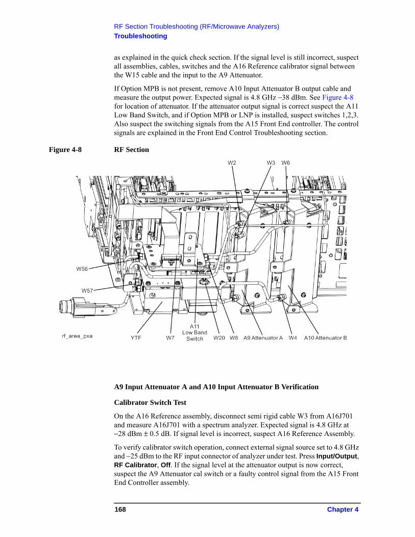
RF Section Troubleshooting (RF/Microwave Analyzers)
Troubleshooting
as explained in the quick check section. If the signal level is still incorrect, suspect all assemblies, cables, switches and the A16 Reference calibrator signal between the W15 cable and the input to the A9 Attenuator.
If Option MPB is not present, remove A10 Input Attenuator B output cable and measure the output power. Expected signal is 4.8 GHz −38 dBm. See Figure 4-8 for location of attenuator. If the attenuator output signal is correct suspect the A11 Low Band Switch, and if Option MPB or LNP is installed, suspect switches 1,2,3. Also suspect the switching signals from the A15 Front End controller. The control signals are explained in the Front End Control Troubleshooting section.
Figure 4-8 RF Section
A9 Input Attenuator A and A10 Input Attenuator B Verification
Calibrator Switch Test
On the A16 Reference assembly, disconnect semi rigid cable W3 from A16J701 and measure A16J701 with a spectrum analyzer. Expected signal is 4.8 GHz at −28 dBm ± 0.5 dB. If signal level is incorrect, suspect A16 Reference Assembly.
To verify calibrator switch operation, connect external signal source set to 4.8 GHz and −25 dBm to the RF input connector of analyzer under test. Press Input/Output, RF Calibrator, Off. If the signal level at the attenuator output is now correct, suspect the A9 Attenuator cal switch or a faulty control signal from the A15 Front End Controller assembly.
168 Chapter 4
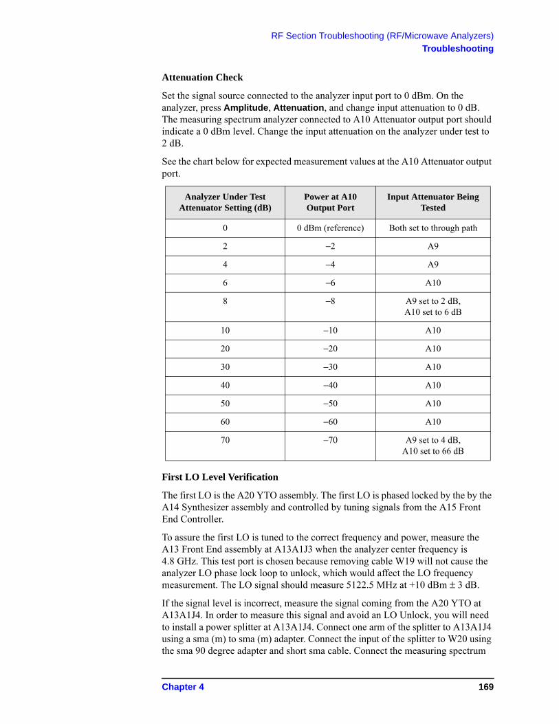
RF Section Troubleshooting (RF/Microwave Analyzers)
Troubleshooting
Attenuation Check
Set the signal source connected to the analyzer input port to 0 dBm. On the analyzer, press Amplitude, Attenuation, and change input attenuation to 0 dB. The measuring spectrum analyzer connected to A10 Attenuator output port should indicate a 0 dBm level. Change the input attenuation on the analyzer under test to 2 dB.
See the chart below for expected measurement values at the A10 Attenuator output port.
First LO Level Verification
The first LO is the A20 YTO assembly. The first LO is phased locked by the by the A14 Synthesizer assembly and controlled by tuning signals from the A15 Front End Controller.
To assure the first LO is tuned to the correct frequency and power, measure the A13 Front End assembly at A13A1J3 when the analyzer center frequency is 4.8 GHz. This test port is chosen because removing cable W19 will not cause the analyzer LO phase lock loop to unlock, which would affect the LO frequency measurement. The LO signal should measure 5122.5 MHz at +10 dBm ± 3 dB.
If the signal level is incorrect, measure the signal coming from the A20 YTO at A13A1J4. In order to measure this signal and avoid an LO Unlock, you will need to install a power splitter at A13A1J4. Connect one arm of the splitter to A13A1J4 using a sma (m) to sma (m) adapter. Connect the input of the splitter to W20 using the sma 90 degree adapter and short sma cable. Connect the measuring spectrum
Analyzer Under TestAttenuator Setting (dB)
Power at A10 Output Port
Input Attenuator Being Tested
0 0 dBm (reference) Both set to through path
2 −2 A9
4 −4 A9
6 −6 A10
8 −8 A9 set to 2 dB, A10 set to 6 dB
10 −10 A10
20 −20 A10
30 −30 A10
40 −40 A10
50 −50 A10
60 −60 A10
70 −70 A9 set to 4 dB, A10 set to 66 dB
Chapter 4 169
RF Section Troubleshooting (RF/Microwave Analyzers)
Troubleshooting
analyzer to the other arm of the splitter. Add the loss through the splitter arm which is 6 dB for the Agilent 11667B splitter. The signal should be 5122.5 MHz at +10 dBm ± 3 dB.
When measuring A13A1J5, Synth Out, the splitter must also be used. The expected signal level is 5122.5 MHz at +10 dBm ± 3 dB
A13 Front End Assembly Verification
NOTE The A13 Front End assembly is shown as A13A1 and A13A2 for troubleshooting clarification. However, A13A1 and A13A2 are not separately replaceable. The entire A13 assembly must be replaced.
Many portions of the Front End Assembly have been verified earlier in the High Band troubleshooting process outlined above.
The input signal level was measured on W15 as part of the A13 Front End Input Verification.
The output signal level was measured at A13A1J7 during the quick check to verify the High Band signal path.
The LO input at W20, and the LO outputs were tested when performing the First LO Verification.
High Band Preamp (Option P08, P13, P26)
If a preamp option listed above is installed, the High Band preamp can be verified as follows:
View the 4.8 GHz calibrator signal on screen. Press AMPTD, More, Internal Preamp, Full Range to activate the preamp.The expected operation is the signal level will not change more than +/- 0.5 dB and the noise floor will increase due to the fact the input attenuation was automatically increased.
If the amplitude error when switching the preamp on and off is greater than 0.5 dB, assure that any other internal alignment failures are resolved since the System Gain alignment must run before optimum performance is possible. The amplitude error could be caused by poor frequency response, and performing the high band frequency response adjustment (using the calibration software) will adjust the preamp on, high band path. Assure you have evaluated all causes including A15 Front End Controller switching problems, before you replace the Front End assembly.
170 Chapter 4
RF Section Troubleshooting (RF/Microwave Analyzers)
Troubleshooting
High Band Mixing Equations
For input signal frequencies from 3.6 GHz to 8.4 GHz and 13.6 GHz to 17 GHz:
RF = LO x N − IFIF = LO x N − RFLO x N = IF + RF
where RF is the input signal at the signal analyzerwhere N is the harmonic mixing mode:
N = 1 for 3.5 GHz to 8.4 GHzN = 2 for 13.5 GHz to 17 GHz
For input signal frequencies above 8.4 GHz to 13.6 GHzand 17 GHz to 26.5 GHz:
RF = LO x 2 x N − IFIF = LO x 2 x N − RFLO x 2 x N = RF + IF
where RF is the input signal at the signal analyzerwhere N is the harmonic mixing mode:
N = 1 for 8.4 GHz to 13.6 GHzN = 2 for 17 GHz to 26.5 GHz
Low Noise Path (Option LNP)
Allows the Lowband Switch assembly to be bypassed, improving sensitivity in highband path.
Press Amplitude, uW Path Control, Low Noise Path Enable key. The Low Noise Path will be enabled only after the following conditions are met:
1. The start frequency must be 3.6 GHz or greater.
2. The high band preamp (option P08, P18, P26) must be Off.
When Switch 3 changes state, you will hear a click. The amplitude of the displayed signal should not change.
Microwave Preselector Bypass (Option MPB)
Allows the YTF to be bypassed improving amplitude accuracy.
Assure start frequency is 3.6 GHz or greater. Press Amplitude, uW Path Control, uW Preselector Bypass.
When the bypass switches Switch 1 and Switch 2 change state you will hear a click. Depending on the signal source connected, you may see many “signals” appear on screen because without preselection, the analyzer will display images and multiples. The real input signal should not change amplitude when you switch the uW Preselector Bypass on and off.
Chapter 4 171

RF Section Troubleshooting (RF/Microwave Analyzers)
Troubleshooting
172 Chapter 4
5 RF Section Troubleshooting(Millimeter-Wave Analyzers)
173
RF Section Troubleshooting (Millimeter-Wave Analyzers)
What You Will Find in This Chapter
What You Will Find in This Chapter
The following information is found in this chapter:
1. Theory of operation of the RF section.2. Isolating the cause of an hardware problem by verifying the functionality of
assemblies in the RF section signal path.
NOTE Each section describes how the assembly works and gives information to help you troubleshoot the assembly. Each description covers the purpose of the assembly, describes the main components, and lists external connections to the assembly.
The following sections are found in this chapter:
RF Section Description on page 175
Quick Check to Verify the Low Band Signal Path on page 181
Troubleshooting a Low Band Problem on page 184
Quick Check to Verify High Band RF Path on page 189
Troubleshooting a High Band Problem on page 193
174 Chapter 5
RF Section Troubleshooting (Millimeter-Wave Analyzers)
RF Section Description
RF Section Description
This section covers only those optional frequency ranges listed below for the N9030A Signal Analyzer.
• Option 543, 43 GHz Frequency Range
• Option 544, 44 GHz Frequency Range
• Option 550, 50 GHz Frequency Range
The RF input signal can be routed through four different front end signal paths. These various paths are switched in and out based on where the signal analyzer center frequency is tuned.
1. Low band RF path is used when the input frequency is ≤ 3600 MHz
2. High band RF path #1 is used when the input frequency is > 3.6 GHz to 17.1 GHz
3. High band RF path #2 is used when the input frequency is > 17 GHz to 34.5 GHz
4. High band RF Path #3 is used when the input frequency is > 34.4 GHz to 50 GHz
The RF section is designed to convert RF input signals to an intermediate frequency that is present at the RF output of the A13 Front End assembly. This intermediate frequency (IF) depends on installed options and the IF path selected. This chapter will assume the default operation in Spectrum Analyzer mode. Therefore the IF frequency will be 322.5 MHz.
IF Path IF Mode
10 MHz (standard) 322.5 MHz Spectrum Analyzer or IQ Analyzer
25 MHz (Option B25) 322.5 MHz IQ Analyzer
40 MHz (Option B40) 250 MHz IQ Analyzer
140 MHz (Option B1X) 300 MHz IQ Analyzer
160 MHz (Option B1X & B1Y) 300 MHz IQ Analyzer
Chapter 5 175
RF Section Troubleshooting (Millimeter-Wave Analyzers)
RF Section Description
The RF section is comprised of the following major assemblies:
• A9 Input Attenuator A
• A10 Input Attenuator B
• A11 Low Band Switch Assembly
• A12 YTF Preselector
• A20 Yig Tuned Oscillator
• A13 RF Front End Assembly - shown on the block diagram as A13A1 and A13A2, however the entire A13 assembly must be replaced.
• A15 Front End Control Assembly
• Option LNP - Low Noise Path
• Option MPB - Microwave Preselector Bypass
1. RF input frequencies < 3600 MHz route through the low band path. Refer to the RF Lowband Path Block Diagram in Chapter 13 for details.
The RF input signal level can be optimized by Input Attenuator A and/or Input Attenuator B. The low band switch assembly contains a limiter that offers added protection for the mixer, and routes the input signal to the low band input of the A13 RF Front End assembly. There are (3) different signal paths on the input of the RF Front End assembly that the signal can be routed through depending on installed options and front panel settings.
• Electronic Attenuator path, 0-24 dB (Option EA3)• Low Band Preamplifier path, 20 dB nominal gain (Any preamp option)• Direct to Mixer #1
NOTE The RF input signal can route through the Electronic Attenuator section or the Preamplifier, but not both. All RF input frequencies < 3600 MHz go to Mixer #1.
The RF input signal is then mixed with the 1st LO from the A20 YTO assembly
to a 1st intermediate frequency of 5122.5 MHz. Since the RF input signal is <3600 MHz for low band, this RF input signal is upconverted in Mixer #1 to
the 1st IF. This 1st IF signal is then downconverted in Mixer #2 using the
4800 MHz 2nd LO generated on the A16 Reference assembly to a 2nd
intermediate frequency of 322.5 MHz (5122.5 MHz (1st IF) − 4800 MHz
(2nd LO)). The 2nd IF output is at A13A1J7. This signal path is used for all frequency range options when the RF input frequencies are < 3600 MHz. The control voltages and biasing for these assemblies come from the A15 Front End Control assembly.
176 Chapter 5
RF Section Troubleshooting (Millimeter-Wave Analyzers)
RF Section Description
2. RF input frequencies from 3.6 GHz to 17.1 GHz go through the high band path. Refer to the RF Highband Path #1 Block Diagram (Millimeter-Wave Analyzers) in Chapter 13 for details.
The input signal level can be optimized by Input Attenuator A and/or Input Attenuator B. The Low Band Switch assembly routes the signal through the A12 YTF Preselector. If one of the optional high band preamps is licensed, the signal can be routed through the preamp. The A15 Front End Controller provides switching signals.
The Low Band Switch assembly performs the following tasks:
• Provides a limiter that offers added protection for the mixer and optional preamp.
• Contains the high band preamp.• Routes the input signal to either the low band input of the A13 Front End
assembly or to the A12 YTF Preselector. If Options LNP or MPB are installed, the signal is routed through switches.
The high band input switch in the Front End Assembly routes the RF input
signal to Mixer #2, where it mixes with the LO and provides a 1st intermediate frequency of 322.5 MHz. The 322.5 MHz IF output is at A13A1J7. The control voltages and biasing are provided by the A15 Front End Control Assembly. The LO is doubled for tuned frequencies > 8.4 GHz in this path.
3. RF input frequencies from 17.1 GHz to 34.5 GHz go through the high band path. Refer to the RF Highband Path #2 Block Diagram (Millimeter-Wave Analyzers) in Chapter 13 for details.
The signal path for 17.1 GHz to 34.5 GHz operation is almost the same as the 3.6 GHz to 17.1 GHz path. The only difference is that Mixer #3 is used in this path. The LO is doubled for all tuned frequencies in this path.
4. RF input frequencies from 34.5 GHz to 50 GHz go through the high band path. Refer to the RF Highband Path #3 Block Diagram (Millimeter-Wave Analyzers) in Chapter 13 for details.
The signal path for 34.5 GHz to 50 GHz operation is almost the same as the 3.6 GHz to 17.1 GHz path. The only difference is that Mixer #4 is used in this path. The LO is doubled for all tuned frequencies in this path.
A9 Input Attenuator A
This assembly has two 2 dB attenuator sections, a 6 dB attenuator section, and a cal signal input port.
A10 Input Attenuator B
This assembly has a total of 60 dB of attenuation to control the signal level into the Low Band Switch assembly. There is a 10 dB, 20 dB, and 30 dB section in the A10 assembly. Total input attenuation with the A9 and the A10 combined is 70 dB in 2 dB steps.
Chapter 5 177
RF Section Troubleshooting (Millimeter-Wave Analyzers)
RF Section Description
A11 Low Band Switch
This assembly operates across the entire frequency range of the analyzer. The switch has 3 main functions:
• Switch RF input frequencies from 3 Hz to 3.59 GHz RF Output to A13 RF Front End Assembly.
• Switch input frequencies from 3.6 GHz to 50 GHz Millimeter-Wave RF Output to A12, YTF Preselector.
• Contains optional high band preamplifier, which has a typical gain of 35 dB to 40 dB and a noise figure from 9 to 23 dB up to 50 GHz.
A12 YTF Preselector
The YTF Preselector is used for input frequencies greater than 3.6 GHz. Signals less than 3.6 GHz bypass the YTF assembly and are routed to the low band input of the A13 RF Front End Assembly. The YTF Preselector is a YIG tunable bandpass filter whose main purpose is to track the input signal and to filter out unwanted spurious or image response signals. The YTF Preselector has a 3 dB bandwidth greater than 40 MHz and an insertion loss of ~ 6.5 dB.
The preselector requires centering for optimum amplitude accuracy. The Auto Align routine will perform a rough centering during the preselector two point tuning algorithm. However, when troubleshooting, press Amplitude, Preselector Center to manually center the preselector.
A20 YTO Assembly
Provides the 1st LO signal that is required for the A13 RF Front End Assembly.
The 1st LO has a frequency range from 3.80 to 8.73 GHz. The output power is +13 to +18 dBm. In order to maximize the conversion efficiency and avoid LO unlock, sufficient LO power must be supplied.
178 Chapter 5
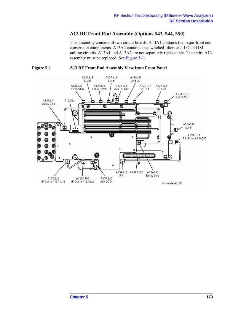
RF Section Troubleshooting (Millimeter-Wave Analyzers)
RF Section Description
A13 RF Front End Assembly (Options 543, 544, 550)
This assembly consists of two circuit boards. A13A1 contains the major front end conversion components. A13A2 contains the switched filters and LO and IM nulling circuits. A13A1 and A13A2 are not separately replaceable. The entire A13 assembly must be replaced. See Figure 5-1.
Figure 5-1 A13 RF Front End Assembly View from Front Panel
Chapter 5 179
RF Section Troubleshooting (Millimeter-Wave Analyzers)
RF Section Description
This assembly contains the following circuits:
• Input Low-pass filter (RF input signals < 3.6 GHz)
• Optional Low Band Electronic Attenuator (0-24 dB attenuation control)
• Optional Low Band Preamplifier and Limiter
• RF Mixer #1 (RF input signals < 3.6 GHz)
• 1st LO Sub-system (3.8 GHz to 8.7 GHz)
• 1st IF Amplifier (5122.5 MHz)
• Switched Filters (A13A2) provides wide BW band pass filter (low band)
• LO and IM nulling (A13A2)
• Mixer #2 (RF input signals 3.6 GHz to 17.1 GHz)
• Microwave Input Amplifier
• Mixer #3 (RF input signals 17 GHz to 34.5 GHz)
• Mixer #4 (RF input signals 34.4 GHz to 50 GHz)
• LO Doubler
• External Mixing Diplexer
A15 Front End Control Assembly
Provides the correct biasing and switch control logic to the following RF assemblies:
• Input Attenuator A
• Input Attenuator B
• Low Band Switch
• (Option LNP) Low Noise Path
• YTF Preselector (Input signals > 3.6 GHz)
• (Option MPB) Microwave Preselector Bypass
• Front End Assembly including switched filter
• (Optional) High Band Preamplifier
• (Optional) Low Band Preamplifier
• (Option EA3) Electronic Attenuator (0-24 dB)
NOTE Refer to Chapter 6 , “Front End Control Troubleshooting” for detailed descriptions & troubleshooting procedures
180 Chapter 5
RF Section Troubleshooting (Millimeter-Wave Analyzers)
Troubleshooting
Troubleshooting
Quick Check to Verify the Low Band Signal Path
The analyzer has an internal 50 MHz amplitude reference signal that is used to verify the low band path. This 50 MHz calibrator is used when the analyzer performs many of the internal alignment routines. Therefore, the functionality of the 50 MHz calibrator and low band path are critical to passing Align All Now. Refer to the RF Lowband Path Block Diagram (Millimeter-Wave Analyzers) in Chapter 13 for details. Reference the instrument settings box on the block diagram.
Equipment needed:
Spectrum Analyzer with frequency range to 8 GHz
Signal source with output power 0 dBm and frequency range to at least 3.6 GHz
Power splitter, 11667B or 11667C
2 each, quality SMA or 3.5 mm cables
90° SMA (m) to SMA (f) adapter
MMCX (f) to SMA (f) cable
SMA (f) to SMA (f) adapter
SMA (m) to SMA (m) adapter
3.5mm (f) to 2.4mm (m) adapters (2 required)
NOTE To perform the following checks, it will be necessary to remove the outer cover and the top brace. See Chapter 16 for removal procedures.
Turn the instrument on and allow it to complete its full boot up process to Spectrum Analyzer mode. Use the internal 50 MHz, −25 dBm calibrator signal as a reference for troubleshooting by pressing Mode Preset, Input/Output, RF Calibrator, 50 MHz on the analyzer. Now press FREQ (Channel), 50 MHz, SPAN (X Scale), 1 MHz, Peak Search. The 50 MHz reference signal should measure 50 MHz @ −25 dBm ± 2 dB on the analyzer display. If the power level is within tolerance, the low band path is functioning correctly at 50 MHz. If the power level is incorrect, select the 4.8 GHz RF Calibrator and set the analyzer center frequency to 4.8 GHz. Since several of the same signal path components are shared between low band and high band, determining if the problem appears in both paths is helpful.
To verify the high band path go to “Quick Check to Verify High Band RF Path” on page 189.
If the power level is not within tolerance, press SPAN (X Scale), Zero Span, AMPTD (Y Scale), Attenuation, 10 dB.
Chapter 5 181
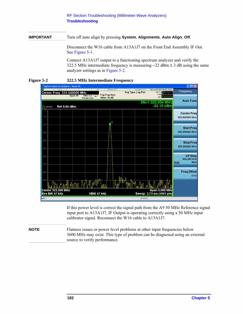
RF Section Troubleshooting (Millimeter-Wave Analyzers)
Troubleshooting
IMPORTANT Turn off auto align by pressing System, Alignments, Auto Align, Off.
Disconnect the W16 cable from A13A1J7 on the Front End Assembly IF Out.See Figure 5-1.
Connect A13A1J7 output to a functioning spectrum analyzer and verify the 322.5 MHz intermediate frequency is measuring −22 dBm ± 3 dB using the same analyzer settings as in Figure 5-2.
Figure 5-2 322.5 MHz Intermediate Frequency
If this power level is correct the signal path from the A9 50 MHz Reference signal input port to A13A1J7, IF Output is operating correctly using a 50 MHz input calibrator signal. Reconnect the W16 cable to A13A1J7.
NOTE Flatness issues or power level problems at other input frequencies below 3600 MHz may exist. This type of problem can be diagnosed using an external source to verify performance.
182 Chapter 5
RF Section Troubleshooting (Millimeter-Wave Analyzers)
Troubleshooting
If this power level is incorrect, the following assemblies need to be verified using the 50 MHz internal calibrator signal. Be sure the 50 MHz calibrator is turned on. Press Input/Output, RF Calibrator, 50 MHz when verifying the performance.
1. A11 Low Band Switch
2. A10 Input Attenuator B
3. A9 Input Attenuator A
4. A16 Reference Assembly (50 MHz calibrator, 2nd LO)
5. A20 YTO
6. A13 RF Front End Assembly
NOTE In order to gain access to the front end components, remove the front frame assembly, but leave the ribbon cable connected so you can still control the instrument. Remove the right side chassis. Refer to the removal procedures in Chapter 16, “Assembly Replacement Procedures”.
Chapter 5 183
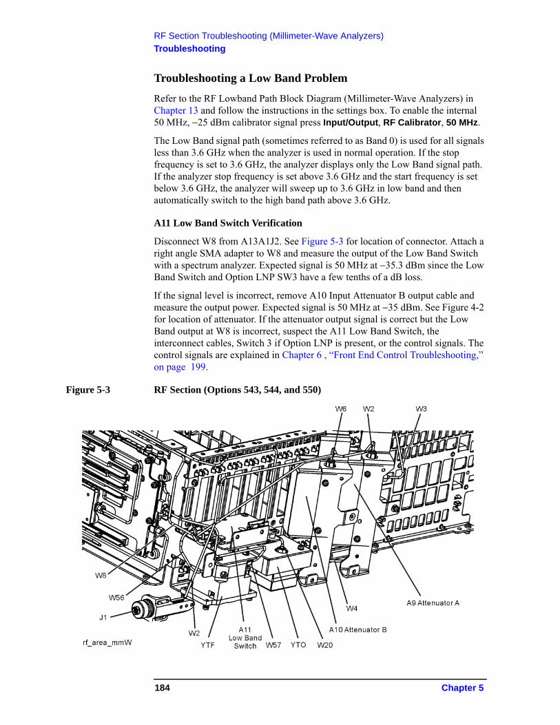
RF Section Troubleshooting (Millimeter-Wave Analyzers)
Troubleshooting
Troubleshooting a Low Band Problem
Refer to the RF Lowband Path Block Diagram (Millimeter-Wave Analyzers) in Chapter 13 and follow the instructions in the settings box. To enable the internal 50 MHz, −25 dBm calibrator signal press Input/Output, RF Calibrator, 50 MHz.
The Low Band signal path (sometimes referred to as Band 0) is used for all signals less than 3.6 GHz when the analyzer is used in normal operation. If the stop frequency is set to 3.6 GHz, the analyzer displays only the Low Band signal path. If the analyzer stop frequency is set above 3.6 GHz and the start frequency is set below 3.6 GHz, the analyzer will sweep up to 3.6 GHz in low band and then automatically switch to the high band path above 3.6 GHz.
A11 Low Band Switch Verification
Disconnect W8 from A13A1J2. See Figure 5-3 for location of connector. Attach a right angle SMA adapter to W8 and measure the output of the Low Band Switch with a spectrum analyzer. Expected signal is 50 MHz at −35.3 dBm since the Low Band Switch and Option LNP SW3 have a few tenths of a dB loss.
If the signal level is incorrect, remove A10 Input Attenuator B output cable and measure the output power. Expected signal is 50 MHz at −35 dBm. See Figure 4-2 for location of attenuator. If the attenuator output signal is correct but the Low Band output at W8 is incorrect, suspect the A11 Low Band Switch, the interconnect cables, Switch 3 if Option LNP is present, or the control signals. The control signals are explained in Chapter 6 , “Front End Control Troubleshooting,” on page 199.
Figure 5-3 RF Section (Options 543, 544, and 550)
184 Chapter 5
RF Section Troubleshooting (Millimeter-Wave Analyzers)
Troubleshooting
A9 Input Attenuator and A10 Input Attenuator Verification
Calibrator Switch Test
On the A16 Reference assembly, disconnect semi rigid cable W3 from A16J701 and measure A16J701 with a spectrum analyzer. Expected signal is 50 MHz at −25 dBm ± 0.5 dB. If signal level is incorrect, suspect A16 Reference assembly is faulty, or the 50 MHz calibrator amplitude requires adjustment using the field calibration software.
To verify calibrator switch operation, connect external signal source set to 50 MHz and −25 dBm to the RF input connector of analyzer under test. Press Input/Output, RF Calibrator, Off. If the signal level at the attenuator output is now correct, suspect the A9 Attenuator cal switch or a faulty control signal from the A15 Front End Controller assembly.
Attenuator Check
Set the signal source connected to the analyzer input port to 0 dBm. On the analyzer, press Amplitude, Attenuation, and change input attenuation to 0 dB. The measuring spectrum analyzer connected to A10 Attenuator output port should indicate a 0 dBm level.
Change the input attenuation on the analyzer under test to 2 dB. See the chart below for expected measurement values at the A10 Attenuator output port.
Analyzer Under TestAttenuator Setting
(dB)
Power at A10 Output Port
(dBm)
Input Attenuator Being Tested
(Options 543, 544, and 550)
0 0 dBm (reference) Both set to through path
2 −2 A9
4 −4 A9
6 −6 A9
8 −8 A9
10 −10 A10
20 −20 A10
30 −30 A10
40 −40 A10
50 −50 A10
60 −60 A10
70 −70 A9 set to 10 dB, A10 set to 60 dB
Chapter 5 185

RF Section Troubleshooting (Millimeter-Wave Analyzers)
Troubleshooting
Second LO Level Verification
The second LO signal comes from the A16 Reference Assembly and is only used in Low Band. The second LO signal can be measured on the Front End Assembly at A13A1J1 or the A16 Reference Assembly at A16J702. Expected signal is 4800 MHz at +10 dBm when a low loss test cable is used and with the measuring spectrum analyzer input attenuator set to at least 20 dB to prevent overload.
First LO Level Verification
The first LO is the A20 YTO assembly. The first LO is phased locked by the A14 Synthesizer assembly and controlled by tuning signals from the A15 Front End Controller.
To assure the first LO is tuned to the correct frequency and power, measure the A13 Front End assembly at A13A1J3 when the analyzer center frequency is 50 MHz. This test port is chosen because removing cable W19 will not cause the analyzer LO phase lock loop to unlock, which would affect the LO frequency measurement.
The LO signal should measure 5172.5 MHz at +10 dBm ± 3 dB.
If the signal level is incorrect, measure the signal coming from the A20 YTO at A13A1J4. In order to measure this signal and avoid an LO Unlock, you will need to install a power splitter at A13A1J4. Connect one arm of the splitter to A13A1J4 using a SMA (m) to SMA (m) adapter. Connect the input of the splitter to W20 using the SMA 90 degree adapter and short SMA cable. Connect the measuring spectrum analyzer to the other arm of the splitter. Add the loss through the splitter arm which is 6 dB for the Agilent 11667B splitter.
The signal should be 5172.5 MHz at +10 dBm ± 3 dB
When measuring A13A1J5, Synth Out, the splitter must also be used. The expected signal level is 5172.5 MHz at +10 dBm ± 3 dB.
A13 Front End Assembly Verification
NOTE The A13 Front End assembly is shown as A13A1 and A13A2 for troubleshooting clarification. However, A13A1 and A13A2 are not separately replaceable. The entire A13 assembly must be replaced.
Many portions of the Front End Assembly have been verified earlier in the Low Band troubleshooting process outlined above.
The input signal level was measured on W8 as part of the A11 Low Band Switch verification.
The output signal level was measured at A13A1J7 during the quick check to verify the Low Band Signal Path.
The Second LO input was tested during the Second LO Verification.
The LO input at W20, and the LO outputs were tested when performing the First LO Verification.
186 Chapter 5
RF Section Troubleshooting (Millimeter-Wave Analyzers)
Troubleshooting
It is possible to measure the W48 input cable to the Switched Filter where it connects to A13A2J2, and the output of the Switched Filter at W49 where it connects to A13A1J11. The A13A2 Switched Filter is not separately replaceable, but being able to determine where the signal level is faulty, can aid in verifying the faulty assembly. See the block diagram for signal levels.
CAUTION When measuring W48, the analyzer must be powered down and ribbon cable W28 on the Switched Filter removed to gain access to W48. Once the measuring spectrum analyzer is connected to W48, the W28 ribbon cable must be reinstalled, and only then can the analyzer be powered back up. The ribbon cable is fragile so it cannot be bent out of the way to access the cable, and should not be removed and installed with power applied.
Electronic Attenuator Test (Option EA3)
The electronic attenuator is aligned as part of the System Gain internal alignment process. See the description of the initial alignments and the location of the alignment history file in the Boot Up and Initialization Troubleshooting chapter. Viewing the Alignment History file will tell you if other alignment tests failed, and reveal which electronic attenuator steps failed.
To verify the electronic attenuator operation on instruments with Option EA3, set up the analyzer to view the 50 MHz calibrator signal on screen. Press Input/Output, RF Calibrator, 50 MHz, Center Frequency, 50 MHz, Span, 500 kHz
Press Peak Search to place a marker on the calibrator signal, then press Marker Delta
Activate the electronic attenuator. Press AMPTD, Attenuation, Enable Elec Atten. Then press Elec Atten.
Press the up arrow key to step through all attenuator steps while monitoring the marker delta readout. The signal level should not change more than 0.4 dB as indicated by the marker delta readout.
If the attenuator switches slowly, or the signal is not present when the electronic attenuator is switched into the signal path or the signal appears only when the attenuator is switched on, suspect the control signals from the A15 Front End Controller are faulty or the A13 Front End assembly is faulty. If the attenuator switches, but the switching error between attenuator settings is greater than ± 0.4 dB, assure that any other internal alignment failures are resolved since the System Gain alignment must run before optimum performance is possible. Assure you have evaluated all causes before you replace the Front End assembly.
If you determine the problem is at a frequency other than 50 MHz, perform the low band flatness adjustment before replacing the Front End assembly.
Chapter 5 187
RF Section Troubleshooting (Millimeter-Wave Analyzers)
Troubleshooting
Low Band Preamp (Option P03, P08, P13, P26, P43, P44, P50)
The Preamp is aligned as part of the System Gain internal alignment process. See the description of the initial alignments and the location of the alignment history file in Chapter 2, “Boot Up and Initialization Troubleshooting,” on page 47. Viewing the Alignment History file will tell you if other alignment tests failed, and reveal pass or fail information for the preamp.
If any of the preamp options are installed, the Low Band preamp can be verified as follows:
Set up the analyzer to view the 50 MHz calibrator signal on screen
Press AMPTD, Attenuation, and verify that the Enable Elec Atten key is set to Off. It is not possible to turn on both the electronic attenuator and preamp at the same time.
Press AMPTD, More, Internal Preamp, Low Band to activate the preamp.
The expected operation is the signal level will not change more than ± 0.5 dB and the noise floor will increase due to the fact the input attenuator is automatically increased. If the amplitude error when switching the preamp on and off is greater than 0.5 dB, assure that any other internal alignment failures are resolved since the System Gain alignment must run before optimum performance is possible. Assure you have evaluated all causes including A15 Front End Controller switching problems, before you replace the Front End assembly.
If you determine the problem is at a frequency other than 50 MHz, perform the low band flatness adjustment before replacing the Front End assembly.
Low Band Mixing Equations
Low Band first mixer:
RF = LO − IFIF = LO − RFLO = IF + RF
where RF is the input signal at the signal analyzer
Low Band second mixer:
RF = LO + IFIF = RF − LOLO = RF − IF
where RF in this case is the first IF signal (signal at A13A1J11)
188 Chapter 5
RF Section Troubleshooting (Millimeter-Wave Analyzers)
Troubleshooting
Quick Check to Verify High Band RF Path
Refer to the RF Highband Path #1 Block Diagram (Options 543, 544, and 550) in Chapter 13 .
The High Band signal path (sometimes referred to as Band 1-Band 6) is used for all signals 3.6 GHz and above. If the start frequency is set to 3.6 GHz and above, the analyzer displays only the High Band signal path. If the analyzer start frequency is below 3.6 GHz and the Stop frequency is set above 3.6 GHz, the analyzer will start sweeping in Low Band up to 3.6 GHz, and then automatically switch to the high band path above 3.6 GHz.
Equipment needed:
Spectrum Analyzer with frequency range to 14 GHz
Signal source with output power 0 dBm and frequency range to at least the maximum frequency of the PXA
Power splitter, 11667C
2 each, quality 2.4 mm cables
90° SMA (m) to SMA (f) adapter
MMCX (f) to SMA (f) cable
SMA (f) to SMA (f) adapter
SMA (m) to SMA (m) adapter
3.5mm (f) to 2.4 mm (m) adapters (2 required)
3.5 mm (m) to 2.4 mm (f) adapter
NOTE To perform the following checks, it will be necessary to remove the outer cover and the top brace. See Chapter 16 for removal procedures.
Turn the instrument on and allow it to complete its full boot up process to Signal Analyzer mode. Use the internal 4.8 GHz, −28 dBm calibrator signal as a reference for troubleshooting by pressing Mode Preset, Input/Output, RF Calibrator, 4.8 GHz on the analyzer. Now press FREQ (Channel), 4.8 GHz, SPAN (X Scale), 1 MHz, Peak Search).
The 4.8 GHz reference signal should measure −28 dBm ± 2 dB on the analyzer display. If the power level is within tolerance, the 3.6 GHz to 17.1 Ghz path is functioning correctly at 4.8 Ghz.
If the power level is incorrect, select the 50 MHz RF calibrator and set the analyzer center frequency to 50 MHz. Since several of the same signal path components are shared between high band and low band, determining if the problem appears in both paths is helpful.
IMPORTANT Turn off auto align by pressing System, Alignments, Auto Align, Off.
Chapter 5 189
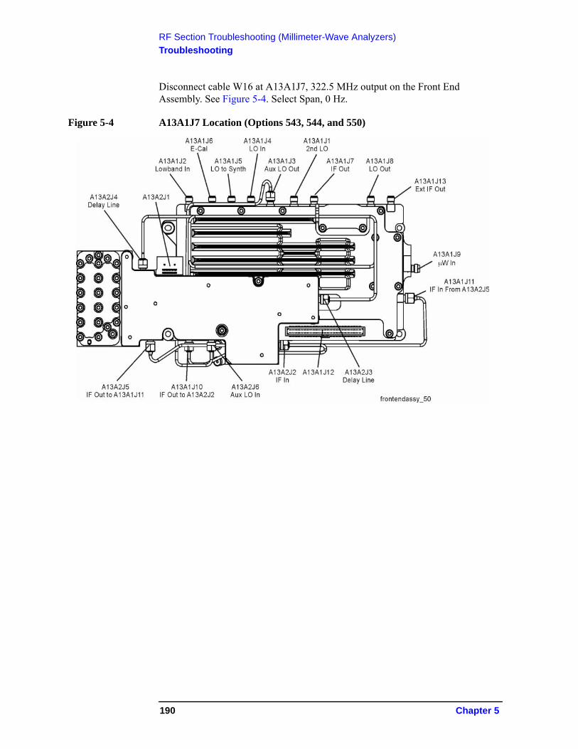
RF Section Troubleshooting (Millimeter-Wave Analyzers)
Troubleshooting
Disconnect cable W16 at A13A1J7, 322.5 MHz output on the Front End Assembly. See Figure 5-4. Select Span, 0 Hz.
Figure 5-4 A13A1J7 Location (Options 543, 544, and 550)
190 Chapter 5

RF Section Troubleshooting (Millimeter-Wave Analyzers)
Troubleshooting
Connect A13J7 output to a functioning spectrum analyzer and verify the 322.5 MHz intermediate frequency is measuring −31 ± 4 dB as shown in Figure 5-5.
Figure 5-5 322.5 MHz Intermediate Frequency
If this power level is correct the Front End assembly is operating correctly in high band. If this power level is incorrect verify the following assemblies using the 4.8 GHz internal calibrator signal.
1. A11 Low Band Switch
2. A10 Input Attenuator B
3. A9 Input Attenuator A
4. A16 Reference Assembly (4.8 GHz calibrator)
5. A20 YTO
6. A12 YTF Preselector
7. A13 Front End Assembly
Chapter 5 191
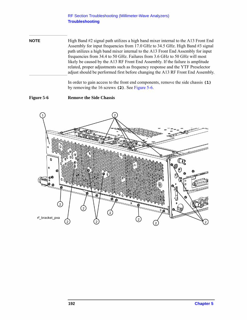
RF Section Troubleshooting (Millimeter-Wave Analyzers)
Troubleshooting
NOTE High Band #2 signal path utilizes a high band mixer internal to the A13 Front End Assembly for input frequencies from 17.0 GHz to 34.5 GHz. High Band #3 signal path utilizes a high band mixer internal to the A13 Front End Assembly for input frequencies from 34.4 to 50 GHz. Failures from 3.6 GHz to 50 GHz will most likely be caused by the A13 RF Front End Assembly. If the failure is amplitude related, proper adjustments such as frequency response and the YTF Preselector adjust should be performed first before changing the A13 RF Front End Assembly.
In order to gain access to the front end components, remove the side chassis (1) by removing the 16 screws (2). See Figure 5-6.
Figure 5-6 Remove the Side Chassis
192 Chapter 5
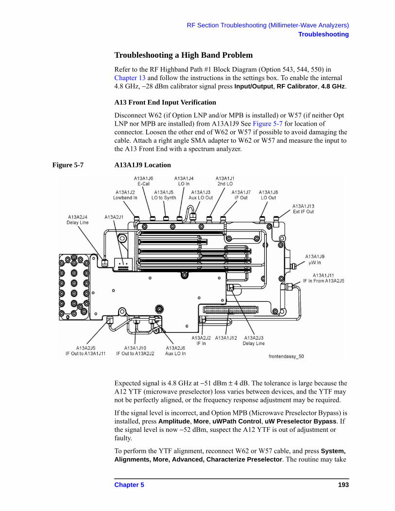
RF Section Troubleshooting (Millimeter-Wave Analyzers)
Troubleshooting
Troubleshooting a High Band Problem
Refer to the RF Highband Path #1 Block Diagram (Option 543, 544, 550) in Chapter 13 and follow the instructions in the settings box. To enable the internal 4.8 GHz, −28 dBm calibrator signal press Input/Output, RF Calibrator, 4.8 GHz.
A13 Front End Input Verification
Disconnect W62 (if Option LNP and/or MPB is installed) or W57 (if neither Opt LNP nor MPB are installed) from A13A1J9 See Figure 5-7 for location of connector. Loosen the other end of W62 or W57 if possible to avoid damaging the cable. Attach a right angle SMA adapter to W62 or W57 and measure the input to the A13 Front End with a spectrum analyzer.
Figure 5-7 A13A1J9 Location
Expected signal is 4.8 GHz at −51 dBm ± 4 dB. The tolerance is large because the A12 YTF (microwave preselector) loss varies between devices, and the YTF may not be perfectly aligned, or the frequency response adjustment may be required.
If the signal level is incorrect, and Option MPB (Microwave Preselector Bypass) is installed, press Amplitude, More, uWPath Control, uW Preselector Bypass. If the signal level is now −52 dBm, suspect the A12 YTF is out of adjustment or faulty.
To perform the YTF alignment, reconnect W62 or W57 cable, and press System, Alignments, More, Advanced, Characterize Preselector. The routine may take
Chapter 5 193
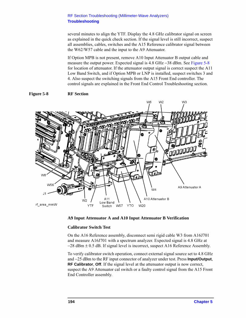
RF Section Troubleshooting (Millimeter-Wave Analyzers)
Troubleshooting
several minutes to align the YTF. Display the 4.8 GHz calibrator signal on screen as explained in the quick check section. If the signal level is still incorrect, suspect all assemblies, cables, switches and the A15 Reference calibrator signal between the W62/W57 cable and the input to the A9 Attenuator.
If Option MPB is not present, remove A10 Input Attenuator B output cable and measure the output power. Expected signal is 4.8 GHz −38 dBm. See Figure 5-8 for location of attenuator. If the attenuator output signal is correct suspect the A11 Low Band Switch, and if Option MPB or LNP is installed, suspect switches 3 and 4. Also suspect the switching signals from the A15 Front End controller. The control signals are explained in the Front End Control Troubleshooting section.
Figure 5-8 RF Section
A9 Input Attenuator A and A10 Input Attenuator B Verification
Calibrator Switch Test
On the A16 Reference assembly, disconnect semi rigid cable W3 from A16J701 and measure A16J701 with a spectrum analyzer. Expected signal is 4.8 GHz at −28 dBm ± 0.5 dB. If signal level is incorrect, suspect A16 Reference Assembly.
To verify calibrator switch operation, connect external signal source set to 4.8 GHz and −25 dBm to the RF input connector of analyzer under test. Press Input/Output, RF Calibrator, Off. If the signal level at the attenuator output is now correct, suspect the A9 Attenuator cal switch or a faulty control signal from the A15 Front End Controller assembly.
194 Chapter 5
RF Section Troubleshooting (Millimeter-Wave Analyzers)
Troubleshooting
Attenuation Check
Set the signal source connected to the analyzer input port to 0 dBm. On the analyzer, press Amplitude, Attenuation, and change input attenuation to 0 dB. The measuring spectrum analyzer connected to A10 Attenuator output port should indicate a 0 dBm level. Change the input attenuation on the analyzer under test to 2 dB.
See the chart below for expected measurement values at the A10 Attenuator output port.
First LO Level Verification
The first LO is the A20 YTO assembly. The first LO is phased locked by the by the A14 Synthesizer assembly and controlled by tuning signals from the A15 Front End Controller.
To assure the first LO is tuned to the correct frequency and power, measure the A13 Front End assembly at A13A1J3 when the analyzer center frequency is 4.8 GHz. This test port is chosen because removing cable W19 will not cause the analyzer LO phase lock loop to unlock, which would affect the LO frequency measurement. The LO signal should measure 5122.5 MHz at +10 dBm ± 3 dB.
If the signal level is incorrect, measure the signal coming from the A20 YTO at A13A1J4. In order to measure this signal and avoid an LO Unlock, you will need to install a power splitter at A13A1J4. Connect one arm of the splitter to A13A1J4 using a SMA (m) to SMA (m) adapter. Connect the input of the splitter to W20 using the SMA 90 degree adapter and short SMA cable. Connect the measuring spectrum analyzer to the other arm of the splitter. Add the loss through the splitter
Analyzer Under TestAttenuator Setting (dB)
Power at A10 Output Port (dBm)
Input Attenuator Being Tested
0 0 dBm (reference) Both set to through path
2 −2 A9
4 −4 A9
6 −6 A9
8 −8 A9
10 −10 A10
20 −20 A10
30 −30 A10
40 −40 A10
50 −50 A10
60 −60 A10
70 −70 A9 set to 10 dB, A10 set to 60 dB
Chapter 5 195
RF Section Troubleshooting (Millimeter-Wave Analyzers)
Troubleshooting
arm which is 6 dB for the Agilent 11667B or 11667C splitter. The signal should be 5122.5 MHz at +10 dBm ± 3 dB.
A13 Front End Assembly Verification
NOTE The A13 Front End assembly is shown as A13A1 and A13A2 for troubleshooting clarification. However, A13A1 and A13A2 are not separately replaceable. The entire A13 assembly must be replaced.
Many portions of the Front End Assembly have been verified earlier in the High Band troubleshooting process outlined above.
The input signal level was measured on W15 as part of the A13 Front End Input Verification.
The output signal level was measured at A13A1J7 during the quick check to verify the High Band signal path.
The LO input at W20, and the LO outputs were tested when performing the First LO Verification.
High Band Preamp (Option P08, P13, P26, P43, P44, P50)
If a preamp option listed above is installed, the High Band preamp can be verified as follows:
View the 4.8 GHz calibrator signal on screen. Press AMPTD, More, Internal Preamp, Full Range to activate the preamp.The expected operation is the signal level will not change more than +/- 0.5 dB and the noise floor will increase due to the fact the input attenuation was automatically increased.
If the amplitude error when switching the preamp on and off is greater than 0.5 dB, assure that any other internal alignment failures are resolved since the System Gain alignment must run before optimum performance is possible. The amplitude error could be caused by poor frequency response, and performing the high band frequency response adjustment (using the calibration software) will adjust the preamp on, high band path. Assure you have evaluated all causes including A15 Front End Controller switching problems, before you replace the Front End assembly.
196 Chapter 5
RF Section Troubleshooting (Millimeter-Wave Analyzers)
Troubleshooting
High Band Mixing Equations
For input signal frequencies from 3.6 GHz to 8.4 GHz:
RF = LO x N − IFIF = LO x N − RFLO x N = IF + RF
where RF is the input signal at the signal analyzerwhere N is the harmonic mixing mode:
N = 1 for 3.5 GHz to 8.4 GHz
For input signal frequencies above 8.4 GHz to 50 GHz:
RF = LO x 2 x N − IFIF = LO x 2 x N − RFLO x 2 x N = RF + IF
where RF is the input signal at the signal analyzerwhere N is the harmonic mixing mode:
N = 1 for 8.4 GHz to 17.1 GHzN = 2 for 17.1 GHz to 34.0 GHzN = 4 for 34.0 GHz to 50 GHz
Low Noise Path (Option LNP)
Allows the Lowband Switch assembly to be bypassed, improving sensitivity in highband path.
Press Amplitude, uW Path Control, Low Noise Path Enable key. The Low Noise Path will be enabled only after the following conditions are met:
1. The start frequency must be 3.6 GHz or greater.
2. The high band preamp (option P08, P18, P26, P43, P44, P50) must be Off.
When Switch 3 changes state, you will hear a click. The amplitude of the displayed signal should not change.
Microwave Preselector Bypass (Option MPB)
Allows the YTF to be bypassed improving amplitude accuracy.
Assure start frequency is 3.6 GHz or greater. Press Amplitude, uW Path Control, uW Preselector Bypass. When the bypass switch, Switch 4, changes state you will hear a click. Depending on the signal source connected, you may see many “signals” appear on screen because without preselection, the analyzer will display images and multiples. The real input signal should not change amplitude when you switch the uW Preselector Bypass on and off.
Chapter 5 197

RF Section Troubleshooting (Millimeter-Wave Analyzers)
Troubleshooting
198 Chapter 5
6 Front End Control Troubleshooting
199
Front End Control Troubleshooting
What You Will Find in This Chapter
What You Will Find in This Chapter
The following information is presented in this chapter:
1. Theory of operation of the Front End Control section.2. Isolating the cause of a hardware problem by verifying the functionality of
assemblies of the Front End Control.
NOTE Each of the following sections first describes how the assembly works, then gives information to help you troubleshoot the assembly. Each description explains the purpose of the assembly, describes the main components, and lists external connections to the assembly.
The following information is found in this chapter:
A15 Front End Control Description on page 201
A15 Front End Control Assembly Troubleshooting on page 205
200 Chapter 6
Front End Control Troubleshooting
A15 Front End Control Description
A15 Front End Control Description
Purpose
The A15 Front End Controller board functionality can be broken down into (3) main categories
1. Provides switch control logic and bias voltages to the major RF front end assemblies in the N9030A Signal Analyzer.
2. Contains on board circuitry providing various signal outputs to other locations within the analyzer.
3. Provides control logic for various instrument options within the analyzer.
These signals are routed to and from the A15 via ribbon cables, wiring harnesses and coaxial cables. The RF front end assemblies require the correct control logic and bias in order to function properly. If the voltages from the A15 are not correct, the RF input signals will most likely be displayed at an incorrect power level if they even get displayed at all.
Standard RF Assemblies Controlled by the A15:
• A9 Input Attenuator A (4 dB total for Opt 503, 508, 513, 526; 10 dB total for Opt 543, 544, 550)
• A10 Input Attenuator B (66 dB total for Opt 503, 508, 513, 526; 60 dB total for Opt 543, 544, 550)
• A11 Low Band Switch
• A12 YIG Tuned Filter
• A13 RF Front End Assembly
A15 On Board Circuits:
• RF Burst Trigger (When set to Relative Trigger or when start frequency is > 300 MHz.)
• Switched IF Filter Control
• 1st L.O. Optimization
• YTF Tune Ramp
• Preselector Tune Out (Provides output voltage, not specified, reserved for future use)
• Mixer Bias
• Amplifier Bias
• Switch Control
Chapter 6 201
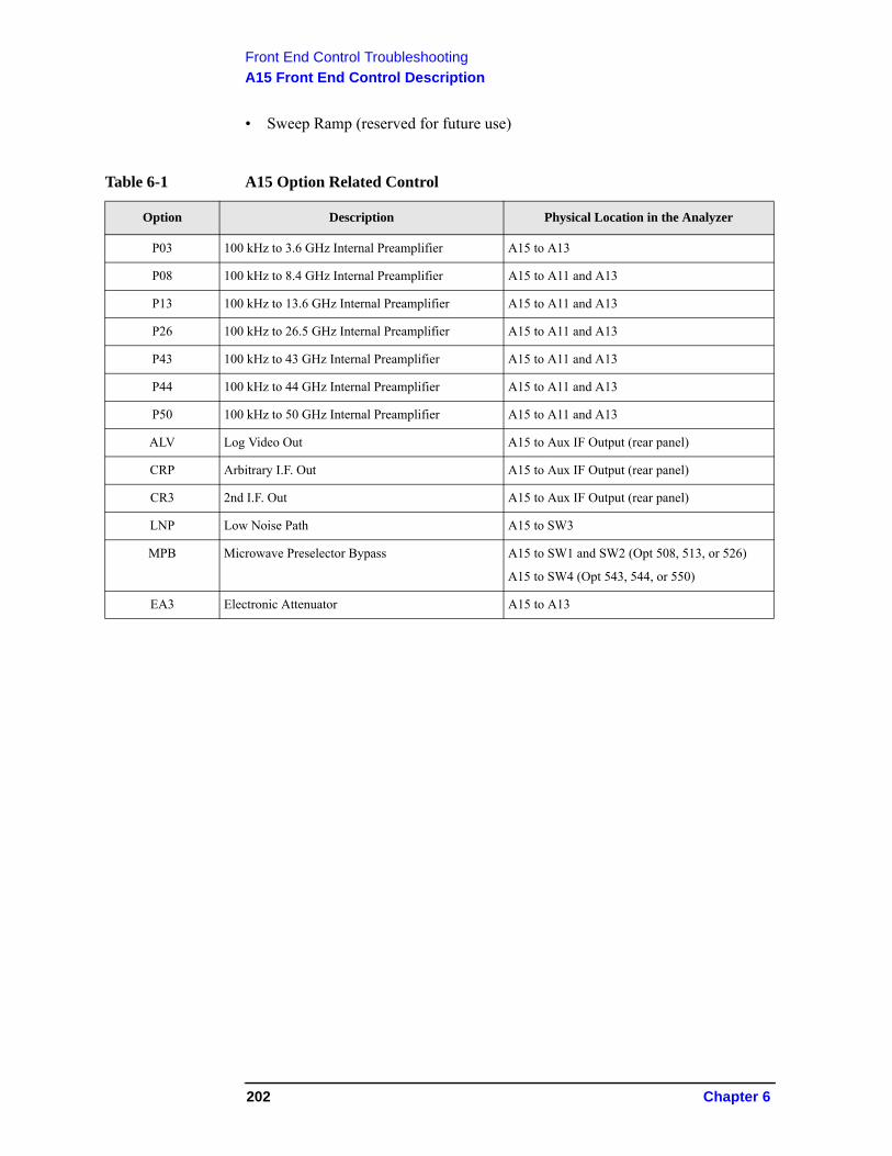
Front End Control Troubleshooting
A15 Front End Control Description
• Sweep Ramp (reserved for future use)
Table 6-1 A15 Option Related Control
Option Description Physical Location in the Analyzer
P03 100 kHz to 3.6 GHz Internal Preamplifier A15 to A13
P08 100 kHz to 8.4 GHz Internal Preamplifier A15 to A11 and A13
P13 100 kHz to 13.6 GHz Internal Preamplifier A15 to A11 and A13
P26 100 kHz to 26.5 GHz Internal Preamplifier A15 to A11 and A13
P43 100 kHz to 43 GHz Internal Preamplifier A15 to A11 and A13
P44 100 kHz to 44 GHz Internal Preamplifier A15 to A11 and A13
P50 100 kHz to 50 GHz Internal Preamplifier A15 to A11 and A13
ALV Log Video Out A15 to Aux IF Output (rear panel)
CRP Arbitrary I.F. Out A15 to Aux IF Output (rear panel)
CR3 2nd I.F. Out A15 to Aux IF Output (rear panel)
LNP Low Noise Path A15 to SW3
MPB Microwave Preselector Bypass A15 to SW1 and SW2 (Opt 508, 513, or 526)
A15 to SW4 (Opt 543, 544, or 550)
EA3 Electronic Attenuator A15 to A13
202 Chapter 6
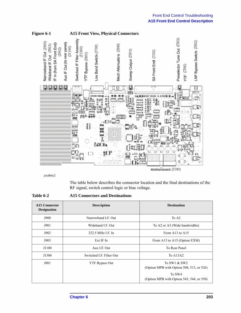
Front End Control Troubleshooting
A15 Front End Control Description
Figure 6-1 A15 Front View, Physical Connectors
The table below describes the connector location and the final destinations of the RF signal, switch control logic or bias voltage.
Table 6-2 A15 Connectors and Destinations
A15 Connector Designation
Description Destination
J900 Narrowband I.F. Out To A2
J901 Wideband I.F. Out To A2 or A3 (Wide bandwidths)
J902 322.5 MHz I.F. In From A13 to A15
J903 Ext IF In From A13 to A15 (Option EXM)
J1100 Aux I.F. Out To Rear Panel
J1300 Switched I.F. Filter Out To A13A2
J801 YTF Bypass Out To SW1 & SW2 (Option MPB with Option 508, 513, or 526)
To SW4(Option MPB with Option 543, 544, or 550)
Chapter 6 203
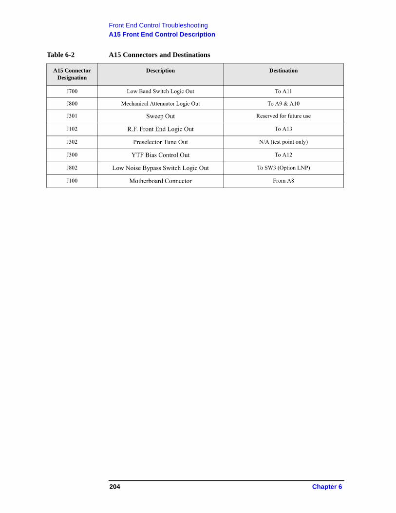
Front End Control Troubleshooting
A15 Front End Control Description
J700 Low Band Switch Logic Out To A11
J800 Mechanical Attenuator Logic Out To A9 & A10
J301 Sweep Out Reserved for future use
J102 R.F. Front End Logic Out To A13
J302 Preselector Tune Out N/A (test point only)
J300 YTF Bias Control Out To A12
J802 Low Noise Bypass Switch Logic Out To SW3 (Option LNP)
J100 Motherboard Connector From A8
Table 6-2 A15 Connectors and Destinations
A15 Connector Designation
Description Destination
204 Chapter 6
Front End Control Troubleshooting
A15 Front End Control Assembly Troubleshooting
A15 Front End Control Assembly Troubleshooting
The N9020A, MXA Signal Analyzer utilizes an RF front end troubleshooting board that can be used to verify some, but not all of the control circuitry on the N9030A, PXA Signal Analyzer due to the additions of front end assemblies. The troubleshooting board kit part number is N9020-60005 and includes the troubleshooting board and required interconnect cables. If you have the interconnect cables, you can order the board by itself using part number E4410-60115. When using the troubleshooting board and cables on a PXA the control logic for Input Attenuator A, Input Attenuator B, Low Band Switch and some of the power supplies can be verified. The remaining control voltages and RF signals can be measured directly with a voltmeter, oscilloscope or functioning spectrum analyzer.
In order to verify the wide bandwidth I.F.'s and Aux I.F. output frequencies and power levels the following specialty cables and connector will be needed:
MMCX (m) to SMB (f) cable, p/n 8121-0655
MMCX (f) to MMCX (f) barrel. Huber & Suhner 31_mmcx-50-0-1/111_0E
Visit: http://www.hubersuhner.com/de/ie70/hs-index
Other standard cables and connectors need to be used to adapt to the voltmeter or the RF input of the functioning spectrum analyzer.
Chapter 6 205
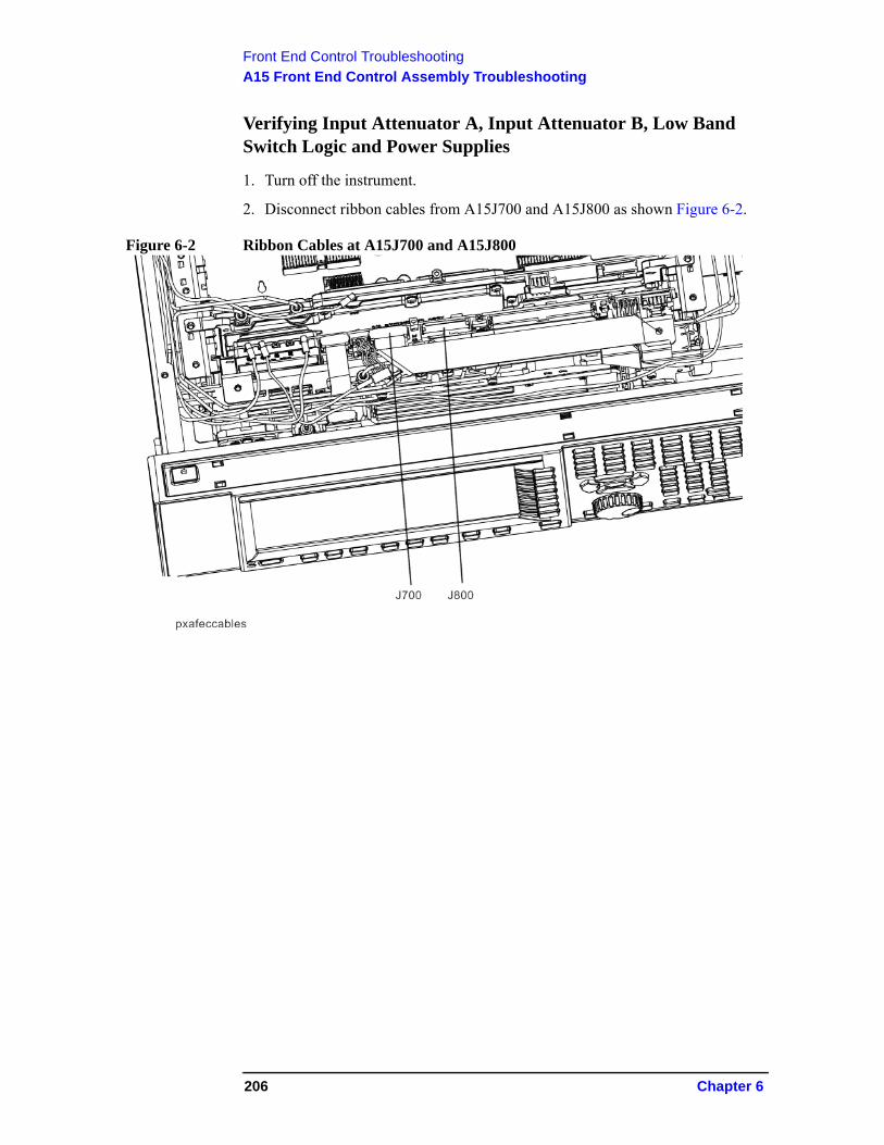
Front End Control Troubleshooting
A15 Front End Control Assembly Troubleshooting
Verifying Input Attenuator A, Input Attenuator B, Low Band Switch Logic and Power Supplies
1. Turn off the instrument.
2. Disconnect ribbon cables from A15J700 and A15J800 as shown Figure 6-2.
Figure 6-2 Ribbon Cables at A15J700 and A15J800
206 Chapter 6
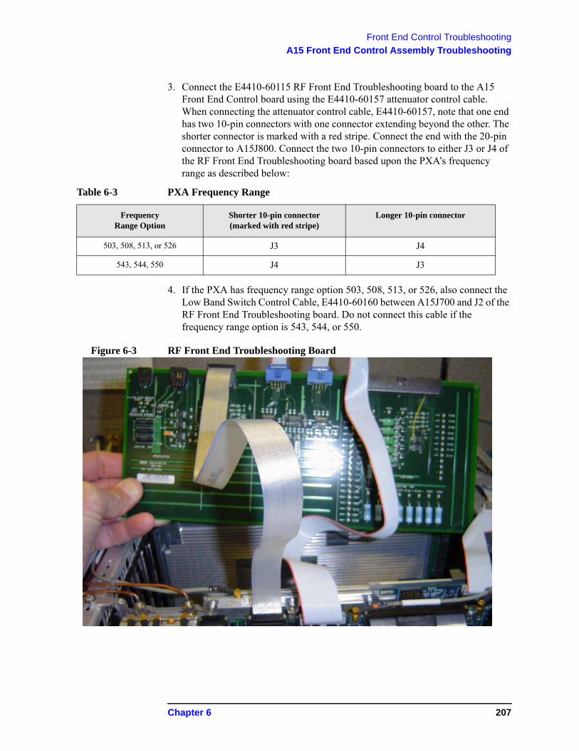
Front End Control Troubleshooting
A15 Front End Control Assembly Troubleshooting
3. Connect the E4410-60115 RF Front End Troubleshooting board to the A15 Front End Control board using the E4410-60157 attenuator control cable. When connecting the attenuator control cable, E4410-60157, note that one end has two 10-pin connectors with one connector extending beyond the other. The shorter connector is marked with a red stripe. Connect the end with the 20-pin connector to A15J800. Connect the two 10-pin connectors to either J3 or J4 of the RF Front End Troubleshooting board based upon the PXA’s frequency range as described below:
4. If the PXA has frequency range option 503, 508, 513, or 526, also connect the Low Band Switch Control Cable, E4410-60160 between A15J700 and J2 of the RF Front End Troubleshooting board. Do not connect this cable if the frequency range option is 543, 544, or 550.
Figure 6-3 RF Front End Troubleshooting Board
Table 6-3 PXA Frequency Range
FrequencyRange Option
Shorter 10-pin connector (marked with red stripe)
Longer 10-pin connector
503, 508, 513, or 526 J3 J4
543, 544, 550 J4 J3
Chapter 6 207
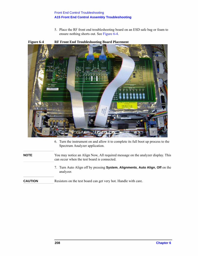
Front End Control Troubleshooting
A15 Front End Control Assembly Troubleshooting
5. Place the RF front end troubleshooting board on an ESD safe bag or foam to ensure nothing shorts out. See Figure 6-4.
Figure 6-4 RF Front End Troubleshooting Board Placement
6. Turn the instrument on and allow it to complete its full boot up process to the Spectrum Analyzer application.
NOTE You may notice an Align Now, All required message on the analyzer display. This can occur when the test board is connected.
7. Turn Auto Align off by pressing System, Alignments, Auto Align, Off on the analyzer.
CAUTION Resistors on the test board can get very hot. Handle with care.
208 Chapter 6
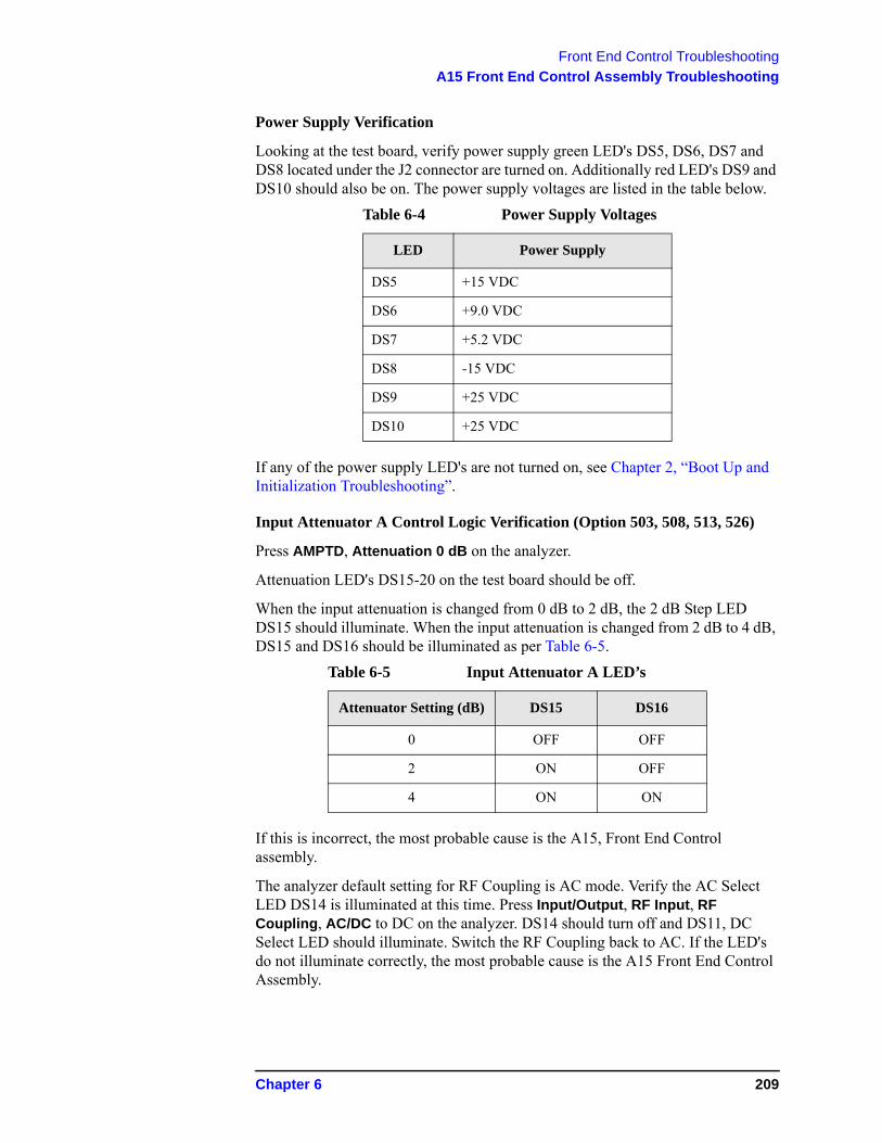
Front End Control Troubleshooting
A15 Front End Control Assembly Troubleshooting
Power Supply Verification
Looking at the test board, verify power supply green LED's DS5, DS6, DS7 and DS8 located under the J2 connector are turned on. Additionally red LED's DS9 and DS10 should also be on. The power supply voltages are listed in the table below.
If any of the power supply LED's are not turned on, see Chapter 2, “Boot Up and Initialization Troubleshooting”.
Input Attenuator A Control Logic Verification (Option 503, 508, 513, 526)
Press AMPTD, Attenuation 0 dB on the analyzer.
Attenuation LED's DS15-20 on the test board should be off.
When the input attenuation is changed from 0 dB to 2 dB, the 2 dB Step LED DS15 should illuminate. When the input attenuation is changed from 2 dB to 4 dB, DS15 and DS16 should be illuminated as per Table 6-5.
If this is incorrect, the most probable cause is the A15, Front End Control assembly.
The analyzer default setting for RF Coupling is AC mode. Verify the AC Select LED DS14 is illuminated at this time. Press Input/Output, RF Input, RF Coupling, AC/DC to DC on the analyzer. DS14 should turn off and DS11, DC Select LED should illuminate. Switch the RF Coupling back to AC. If the LED's do not illuminate correctly, the most probable cause is the A15 Front End Control Assembly.
Table 6-4 Power Supply Voltages
LED Power Supply
DS5 +15 VDC
DS6 +9.0 VDC
DS7 +5.2 VDC
DS8 -15 VDC
DS9 +25 VDC
DS10 +25 VDC
Table 6-5 Input Attenuator A LED’s
Attenuator Setting (dB) DS15 DS16
0 OFF OFF
2 ON OFF
4 ON ON
Chapter 6 209
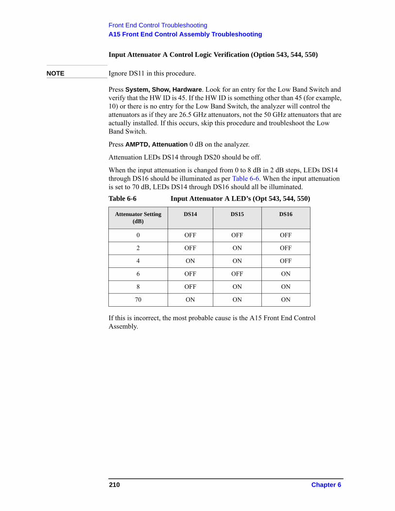
Front End Control Troubleshooting
A15 Front End Control Assembly Troubleshooting
Input Attenuator A Control Logic Verification (Option 543, 544, 550)
NOTE Ignore DS11 in this procedure.
Press System, Show, Hardware. Look for an entry for the Low Band Switch and verify that the HW ID is 45. If the HW ID is something other than 45 (for example, 10) or there is no entry for the Low Band Switch, the analyzer will control the attenuators as if they are 26.5 GHz attenuators, not the 50 GHz attenuators that are actually installed. If this occurs, skip this procedure and troubleshoot the Low Band Switch.
Press AMPTD, Attenuation 0 dB on the analyzer.
Attenuation LEDs DS14 through DS20 should be off.
When the input attenuation is changed from 0 to 8 dB in 2 dB steps, LEDs DS14 through DS16 should be illuminated as per Table 6-6. When the input attenuation is set to 70 dB, LEDs DS14 through DS16 should all be illuminated.
If this is incorrect, the most probable cause is the A15 Front End Control Assembly.
Table 6-6 Input Attenuator A LED’s (Opt 543, 544, 550)
Attenuator Setting (dB)
DS14 DS15 DS16
0 OFF OFF OFF
2 OFF ON OFF
4 ON ON OFF
6 OFF OFF ON
8 OFF ON ON
70 ON ON ON
210 Chapter 6
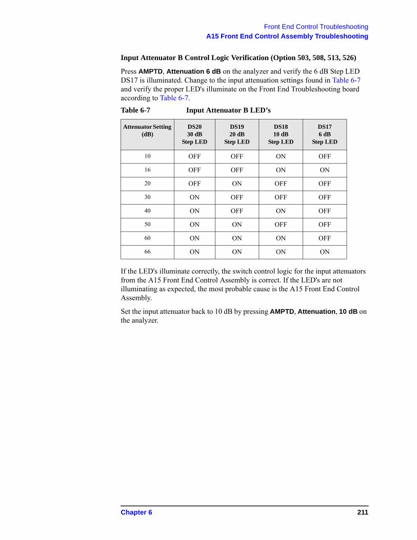
Front End Control Troubleshooting
A15 Front End Control Assembly Troubleshooting
Input Attenuator B Control Logic Verification (Option 503, 508, 513, 526)
Press AMPTD, Attenuation 6 dB on the analyzer and verify the 6 dB Step LED DS17 is illuminated. Change to the input attenuation settings found in Table 6-7 and verify the proper LED's illuminate on the Front End Troubleshooting board according to Table 6-7.
If the LED's illuminate correctly, the switch control logic for the input attenuators from the A15 Front End Control Assembly is correct. If the LED's are not illuminating as expected, the most probable cause is the A15 Front End Control Assembly.
Set the input attenuator back to 10 dB by pressing AMPTD, Attenuation, 10 dB on the analyzer.
Table 6-7 Input Attenuator B LED’s
Attenuator Setting (dB)
DS2030 dB
Step LED
DS1920 dB
Step LED
DS1810 dB
Step LED
DS176 dB
Step LED
10 OFF OFF ON OFF
16 OFF OFF ON ON
20 OFF ON OFF OFF
30 ON OFF OFF OFF
40 ON OFF ON OFF
50 ON ON OFF OFF
60 ON ON ON OFF
66 ON ON ON ON
Chapter 6 211
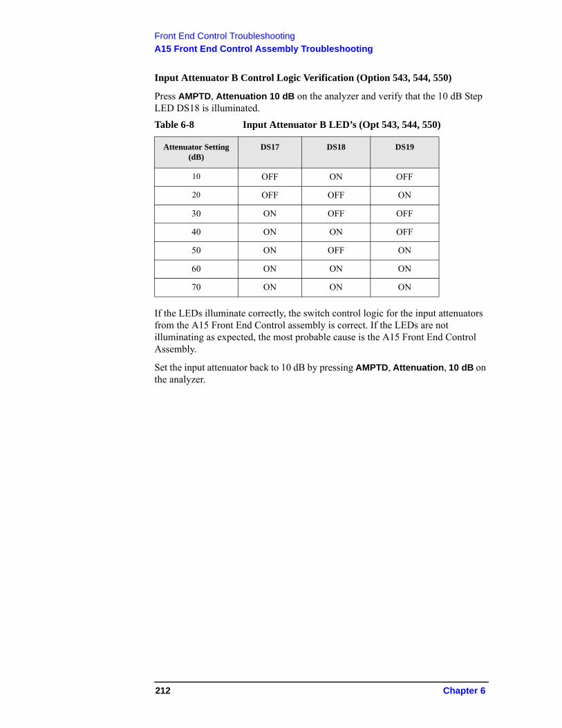
Front End Control Troubleshooting
A15 Front End Control Assembly Troubleshooting
Input Attenuator B Control Logic Verification (Option 543, 544, 550)
Press AMPTD, Attenuation 10 dB on the analyzer and verify that the 10 dB Step LED DS18 is illuminated.
If the LEDs illuminate correctly, the switch control logic for the input attenuators from the A15 Front End Control assembly is correct. If the LEDs are not illuminating as expected, the most probable cause is the A15 Front End Control Assembly.
Set the input attenuator back to 10 dB by pressing AMPTD, Attenuation, 10 dB on the analyzer.
Table 6-8 Input Attenuator B LED’s (Opt 543, 544, 550)
Attenuator Setting (dB)
DS17 DS18 DS19
10 OFF ON OFF
20 OFF OFF ON
30 ON OFF OFF
40 ON ON OFF
50 ON OFF ON
60 ON ON ON
70 ON ON ON
212 Chapter 6
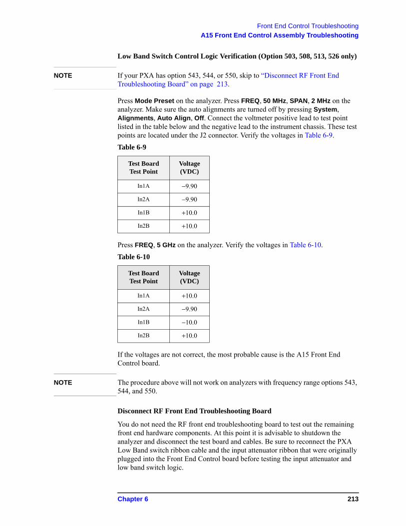
Front End Control Troubleshooting
A15 Front End Control Assembly Troubleshooting
Low Band Switch Control Logic Verification (Option 503, 508, 513, 526 only)
NOTE If your PXA has option 543, 544, or 550, skip to “Disconnect RF Front End Troubleshooting Board” on page 213.
Press Mode Preset on the analyzer. Press FREQ, 50 MHz, SPAN, 2 MHz on the analyzer. Make sure the auto alignments are turned off by pressing System, Alignments, Auto Align, Off. Connect the voltmeter positive lead to test point listed in the table below and the negative lead to the instrument chassis. These test points are located under the J2 connector. Verify the voltages in Table 6-9.
Press FREQ, 5 GHz on the analyzer. Verify the voltages in Table 6-10.
If the voltages are not correct, the most probable cause is the A15 Front End Control board.
NOTE The procedure above will not work on analyzers with frequency range options 543, 544, and 550.
Disconnect RF Front End Troubleshooting Board
You do not need the RF front end troubleshooting board to test out the remaining front end hardware components. At this point it is advisable to shutdown the analyzer and disconnect the test board and cables. Be sure to reconnect the PXA Low Band switch ribbon cable and the input attenuator ribbon that were originally plugged into the Front End Control board before testing the input attenuator and low band switch logic.
Table 6-9
Test Board Test Point
Voltage (VDC)
In1A −9.90
In2A −9.90
In1B +10.0
In2B +10.0
Table 6-10
Test BoardTest Point
Voltage (VDC)
In1A +10.0
In2A −9.90
In1B −10.0
In2B +10.0
Chapter 6 213
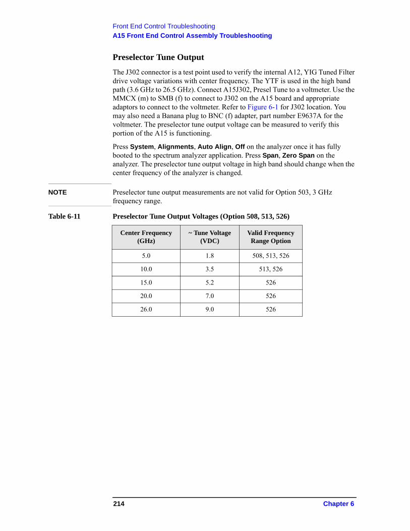
Front End Control Troubleshooting
A15 Front End Control Assembly Troubleshooting
Preselector Tune Output
The J302 connector is a test point used to verify the internal A12, YIG Tuned Filter drive voltage variations with center frequency. The YTF is used in the high band path (3.6 GHz to 26.5 GHz). Connect A15J302, Presel Tune to a voltmeter. Use the MMCX (m) to SMB (f) to connect to J302 on the A15 board and appropriate adaptors to connect to the voltmeter. Refer to Figure 6-1 for J302 location. You may also need a Banana plug to BNC (f) adapter, part number E9637A for the voltmeter. The preselector tune output voltage can be measured to verify this portion of the A15 is functioning.
Press System, Alignments, Auto Align, Off on the analyzer once it has fully booted to the spectrum analyzer application. Press Span, Zero Span on the analyzer. The preselector tune output voltage in high band should change when the center frequency of the analyzer is changed.
NOTE Preselector tune output measurements are not valid for Option 503, 3 GHz frequency range.
Table 6-11 Preselector Tune Output Voltages (Option 508, 513, 526)
Center Frequency (GHz)
~ Tune Voltage (VDC)
Valid Frequency Range Option
5.0 1.8 508, 513, 526
10.0 3.5 513, 526
15.0 5.2 526
20.0 7.0 526
26.0 9.0 526
214 Chapter 6
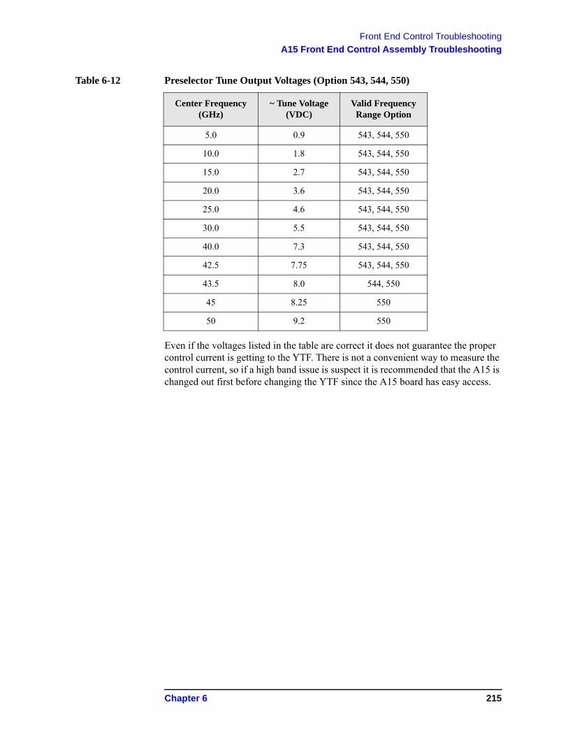
Front End Control Troubleshooting
A15 Front End Control Assembly Troubleshooting
Even if the voltages listed in the table are correct it does not guarantee the proper control current is getting to the YTF. There is not a convenient way to measure the control current, so if a high band issue is suspect it is recommended that the A15 is changed out first before changing the YTF since the A15 board has easy access.
Table 6-12 Preselector Tune Output Voltages (Option 543, 544, 550)
Center Frequency (GHz)
~ Tune Voltage (VDC)
Valid Frequency Range Option
5.0 0.9 543, 544, 550
10.0 1.8 543, 544, 550
15.0 2.7 543, 544, 550
20.0 3.6 543, 544, 550
25.0 4.6 543, 544, 550
30.0 5.5 543, 544, 550
40.0 7.3 543, 544, 550
42.5 7.75 543, 544, 550
43.5 8.0 544, 550
45 8.25 550
50 9.2 550
Chapter 6 215
Front End Control Troubleshooting
A15 Front End Control Assembly Troubleshooting
Verifying SW3 (Option LNP only)
Since there is a ribbon cable from the A15J802 to SW3, it is not feasible to use a voltmeter or oscilloscope to measure the control voltages. For testing SW3, the “click” test can be used.
Press Mode Preset on the analyzer. Press FREQ, 5 GHz, SPAN, 1 MHz. Verify the optional preamplifier is off by pressing AMPTD, More 1 of 2. The Internal Preamp softkey must be Off in order to test SW3. Press AMPTD, More 1 of 2, uW Path Ctrl, Low Noise Path Enable on the analyzer. You should hear a distinct “click” noise from SW3 when the low noise path is selected. Now press uW Path Ctrl and select Standard Path. SW3 will “click” again and return to the standard RF path.
Another way of testing this switch is using an RF signal. This is described in the RF Section Troubleshooting chapter, under the high band troubleshooting section.
Verifying SW1 and SW2 (Option MPB only)
SW1 and SW2 can be verified three different ways:
• “Click” Test
• Oscilloscope
• R.F. Signal Tracing
“Click” Test
This test changes between two different path modes. When this is done a distinct “click” noise from SW1 and SW2 can be heard. Since both switches switch at the same time, it is difficult to decipher if one is switching and the other is not.
Press Mode, Preset on the analyzer. Press FREQ, 5 GHz, SPAN, 1 MHz, AMPTD, More 1 of 2, uW Path Ctrl. Standard Path is the default. Select uW Preselector Bypass and you should hear a distinct “click” noise if the control logic from the A15 Front End Control board is getting to SW1 and SW2.
216 Chapter 6
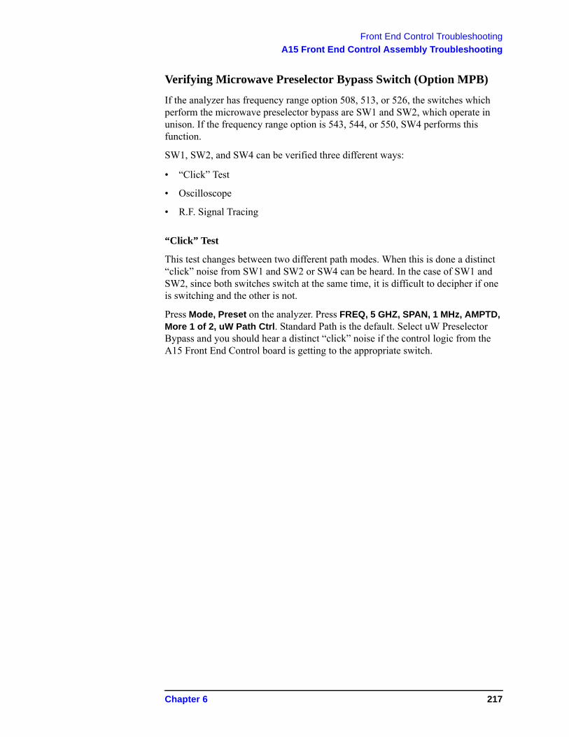
Front End Control Troubleshooting
A15 Front End Control Assembly Troubleshooting
Verifying Microwave Preselector Bypass Switch (Option MPB)
If the analyzer has frequency range option 508, 513, or 526, the switches which perform the microwave preselector bypass are SW1 and SW2, which operate in unison. If the frequency range option is 543, 544, or 550, SW4 performs this function.
SW1, SW2, and SW4 can be verified three different ways:
• “Click” Test
• Oscilloscope
• R.F. Signal Tracing
“Click” Test
This test changes between two different path modes. When this is done a distinct “click” noise from SW1 and SW2 or SW4 can be heard. In the case of SW1 and SW2, since both switches switch at the same time, it is difficult to decipher if one is switching and the other is not.
Press Mode, Preset on the analyzer. Press FREQ, 5 GHZ, SPAN, 1 MHz, AMPTD, More 1 of 2, uW Path Ctrl. Standard Path is the default. Select uW Preselector Bypass and you should hear a distinct “click” noise if the control logic from the A15 Front End Control board is getting to the appropriate switch.
Chapter 6 217
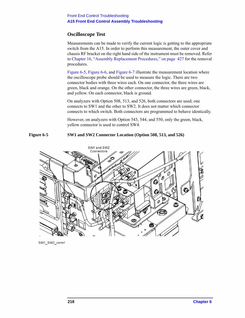
Front End Control Troubleshooting
A15 Front End Control Assembly Troubleshooting
Oscilloscope Test
Measurements can be made to verify the current logic is getting to the appropriate switch from the A15. In order to perform this measurement, the outer cover and chassis RF bracket on the right hand side of the instrument must be removed. Refer to Chapter 16, “Assembly Replacement Procedures,” on page 427 for the removal procedures.
Figure 6-5, Figure 6-6, and Figure 6-7 illustrate the measurement location where the oscilloscope probe should be used to measure the logic. There are two connector bodies with three wires each. On one connector, the three wires are green, black and orange. On the other connector, the three wires are green, black, and yellow. On each connector, black is ground.
On analyzers with Option 508, 513, and 526, both connectors are used; one connects to SW1 and the other to SW2. It does not matter which connector connects to which switch. Both connectors are programmed to behave identically.
However, on analyzers with Option 543, 544, and 550, only the green, black, yellow connector is used to control SW4.
Figure 6-5 SW1 and SW2 Connector Location (Option 508, 513, and 526)
218 Chapter 6
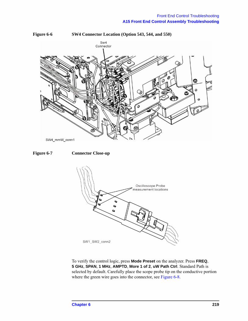
Front End Control Troubleshooting
A15 Front End Control Assembly Troubleshooting
Figure 6-6 SW4 Connector Location (Option 543, 544, and 550)
Figure 6-7 Connector Close-up
To verify the control logic, press Mode Preset on the analyzer. Press FREQ, 5 GHz, SPAN, 1 MHz, AMPTD, More 1 of 2, uW Path Ctrl. Standard Path is selected by default. Carefully place the scope probe tip on the conductive portion where the green wire goes into the connector, see Figure 6-8.
Chapter 6 219
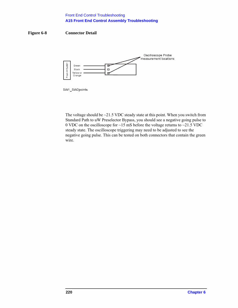
Front End Control Troubleshooting
A15 Front End Control Assembly Troubleshooting
Figure 6-8 Connector Detail
The voltage should be ~21.5 VDC steady state at this point. When you switch from Standard Path to uW Preselector Bypass, you should see a negative going pulse to 0 VDC on the oscilloscope for ~15 mS before the voltage returns to ~21.5 VDC steady state. The oscilloscope triggering may need to be adjusted to see the negative going pulse. This can be tested on both connectors that contain the green wire.
220 Chapter 6
Front End Control Troubleshooting
A15 Front End Control Assembly Troubleshooting
Monitor the yellow or orange wires on each connector, one at a time. The yellow or orange wire starts at ~21.5 VDC. When switching from uW Preselector Bypass to Standard Path, you should see a negative going pulse to 0 VDC on the oscilloscope for ~15 mS before the voltage returns to ~21.5 VDC steady state.
If both the green wires and the yellow or orange wires measure this pulse correctly, the control logic from the A15, Front End Controller board is operating correctly.
The black wire is ground.
RF Signal Tracing
Refer to Chapter 4 , “RF Section Troubleshooting (RF/Microwave Analyzers)” for this method of troubleshooting if you are unable to use an Oscilloscope
Verifying Narrowband IF Out (A15J900)
The outer cover and top shield need to be removed to verify A15J900 I.F. output to the A2 Analog IF assembly. Refer to Chapter 16, “Assembly Replacement Procedures” for the removal procedure. Press Mode, Spectrum Analyzer, Mode Preset on the analyzer. Press Input/Output, RF Calibrator, 50 MHz, Freq, 50 MHz, Span, 0 Hz, Amptd, Attenuation, 10 dB, Amptd, More 1 of 2, Internal Preamp Off, System, Alignments, Auto Align, Off. Disconnect the cable marked J900 that plugs into the top of the A15, Front End Controller board and connect a functioning spectrum analyzer where the cable was plugged in. J900's output should be 322.5 MHz at ~-23 dBm on the functioning spectrum analyzer if the Front End Controller board is switching this level correctly. If -23 dBm is not being measured correctly, remove the cable labeled J902 from the Front End Controller board and measure the output of that cable. This should also measure 322.5 MHz at ~-23 dBm. If the output of the J902 cable measures correctly and yet the output of J900 is incorrect, the most probable cause is the A15, Front End Controller board.
Reconnect all cables to their correct location when finished with the measurements.
IMPORTANT When plugging in an mmcx connector, a distinct “snap” should be heard when the cable is seated correctly.
Chapter 6 221
Front End Control Troubleshooting
A15 Front End Control Assembly Troubleshooting
Verifying Wideband IF Out (A15J901, Option B40 or B1X only)
The outer cover and top shield need to be removed to verify A15J901 output. Refer to Chapter 16, “Assembly Replacement Procedures” for the removal procedure. Press Mode, IQ Analyzer (Basic), Mode Preset on the analyzer. Press Input/Output, RF Calibrator, 50 MHz, Freq, 50 MHz, Amptd, Attenuation, 10 dB, Amptd, More 1 of 2, Internal Preamp Off, System, Alignments, Auto Align, Off. Disconnect the cable marked J901 that plugs into the Front End Controller board and connect a functioning spectrum analyzer where the cable was plugged in. J901's I.F. output will vary depending on the I.F. path that is chosen. Press Mode Setup, IF Path and select 40 MHz. If the switch path is working correctly in the A15 Front End Controller board, the functioning spectrum analyzer should measure 250 MHz at ~-30 dBm.
If Option B1X is installed in the analyzer press Mode Setup, IF Path and select 140 MHz. If the switch path is working correctly in the A15 Front End Controller board, the functioning spectrum analyzer should measure 300 MHz at ~-30 dBm.
In order for these I.F. levels to measure correctly, the I.F. input at A15J902 must be correct. Refer to Chapter 4 , “RF Section Troubleshooting (RF/Microwave Analyzers)”. Reconnect all cables to their correct location when finished.
Verifying Aux IF Out, Rear Panel (Option CR3, CRP, ALV only)
The Aux I.F. output connector on the rear panel of the PXA is installed on each instrument; however the actual Aux I.F. output frequency will vary depending on the options installed. These options are all enabled with a license key. The first step in verifying the Aux I.F. output is the make sure the option is licensed by pressing System, Show, System on the analyzer and make sure the option identifies itself in the table.
The I.F. switch path and frequency generation occurs on the A15, Front End Controller board. This troubleshooting procedure provides the instrument setups to verify options CR3, CRP and ALV. Test the Aux I.F. output based on the options installed in the analyzer.
Standard PXA
No test to perform.
222 Chapter 6
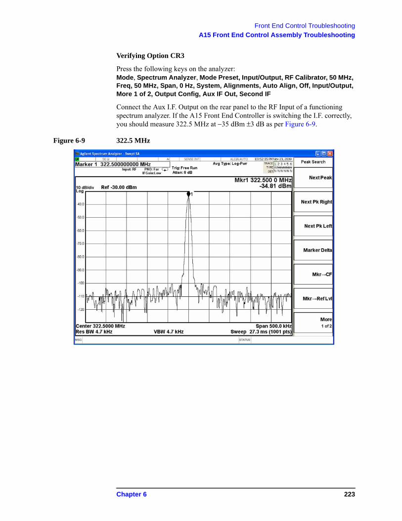
Front End Control Troubleshooting
A15 Front End Control Assembly Troubleshooting
Verifying Option CR3
Press the following keys on the analyzer:Mode, Spectrum Analyzer, Mode Preset, Input/Output, RF Calibrator, 50 MHz, Freq, 50 MHz, Span, 0 Hz, System, Alignments, Auto Align, Off, Input/Output, More 1 of 2, Output Config, Aux IF Out, Second IF
Connect the Aux I.F. Output on the rear panel to the RF Input of a functioning spectrum analyzer. If the A15 Front End Controller is switching the I.F. correctly, you should measure 322.5 MHz at −35 dBm ±3 dB as per Figure 6-9.
Figure 6-9 322.5 MHz
Chapter 6 223
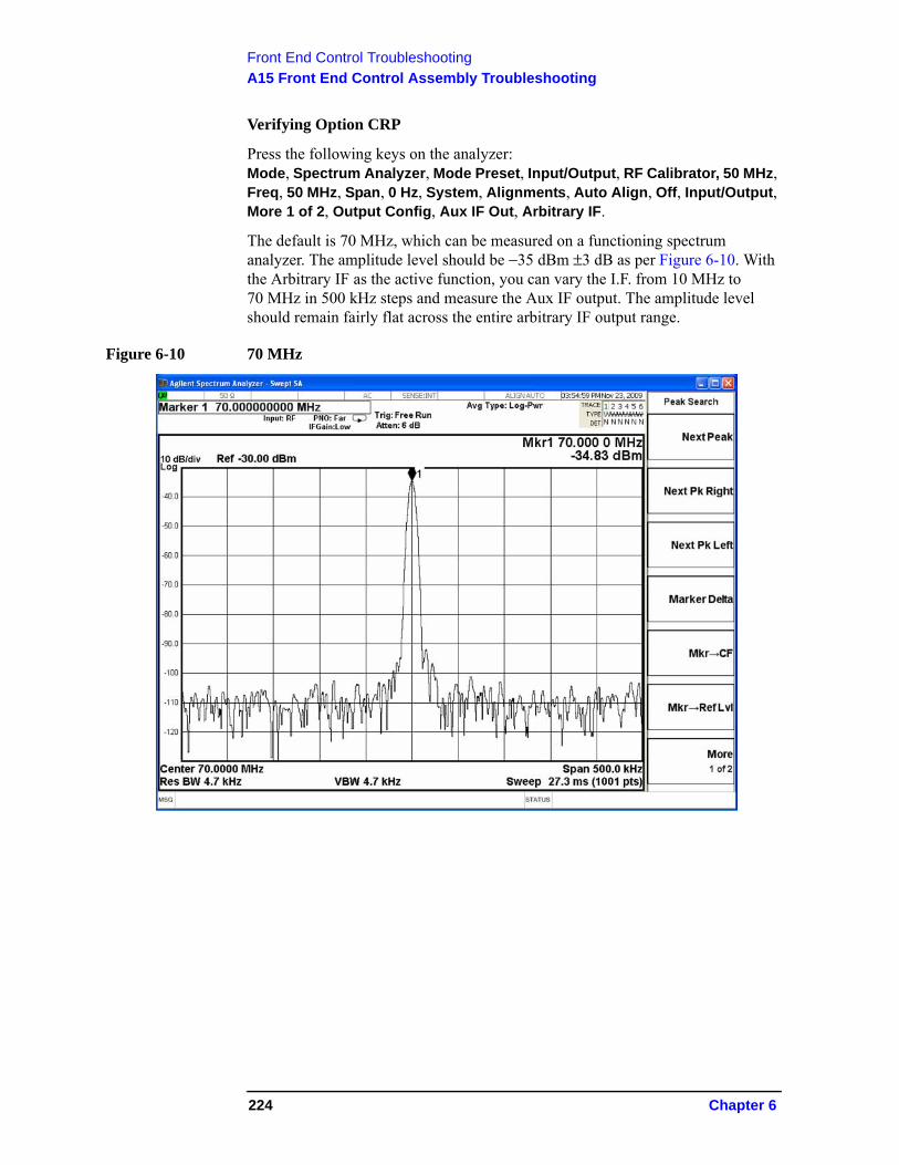
Front End Control Troubleshooting
A15 Front End Control Assembly Troubleshooting
Verifying Option CRP
Press the following keys on the analyzer:Mode, Spectrum Analyzer, Mode Preset, Input/Output, RF Calibrator, 50 MHz, Freq, 50 MHz, Span, 0 Hz, System, Alignments, Auto Align, Off, Input/Output, More 1 of 2, Output Config, Aux IF Out, Arbitrary IF.
The default is 70 MHz, which can be measured on a functioning spectrum analyzer. The amplitude level should be −35 dBm ±3 dB as per Figure 6-10. With the Arbitrary IF as the active function, you can vary the I.F. from 10 MHz to 70 MHz in 500 kHz steps and measure the Aux IF output. The amplitude level should remain fairly flat across the entire arbitrary IF output range.
Figure 6-10 70 MHz
224 Chapter 6
Front End Control Troubleshooting
A15 Front End Control Assembly Troubleshooting
Verifying Option ALV
Equipment needed:
Volt meter
Adapters and cables to connect the volt meter to the Aux IF Out SMA connector on the spectrum analyzer rear panel.
Signal source
Signal source settings:
Frequency: 1 GHz (CW)
Amplitude: −10 dBm
Press the following keys on the analyzer:Mode, Spectrum Analyzer, Mode Preset, FREQ Channel, and set the center frequency to 1 GHz. Press Span, Zero Span, Input/Output, More, Output Config, Aux IF Out, Fast Log Video.
Connect the rear panel Aux IF Out of the signal analyzer to a voltmeter set to measure DC volts.
Verify that signal level appears on the analyzer screen positioned 1 division below top graticule line.
Voltmeter should measure approximately 1.4 Vdc.
Reduce source output power to −20 dBm. Signal should now appear one division lower, and voltmeter should measure approximately 1.2 VDC.
Reduce source output power to −30 dBm. Signal should now appear one division lower, and voltmeter should measure approximately 1.0 VDC.
Chapter 6 225

Front End Control Troubleshooting
A15 Front End Control Assembly Troubleshooting
226 Chapter 6

7 Analog/Digital IF Troubleshooting
227
Analog/Digital IF Troubleshooting
What You Will Find in This Chapter
What You Will Find in This Chapter
The following information is presented in this chapter:
1. Theory of operation of the IF section.2. Isolating the cause of a hardware problem by verifying the functionality of
assemblies in the IF section signal path.
NOTE Each of the following sections first describes how the assembly works, then gives information to help you troubleshoot the assembly. Each description explains the purpose of the assembly, describes the main components, and lists external connections to the assembly.
The following sections are found in this chapter:
• A2 Analog IF Assembly Description on page 229• A2 Analog IF Assembly Theory of Operation on page 230• A2 Analog IF Troubleshooting on page 233• A3 Digital IF Assembly Description on page 240• A3 Digital IF Assembly Theory of Operation on page 241• A3 Digital IF Troubleshooting on page 243
228 Chapter 7
Analog/Digital IF Troubleshooting
A2 Analog IF Assembly Description
A2 Analog IF Assembly Description
When the 10 MHz or 25 MHz IF Path is selected, or when any swept measurement is made, the analyzer's RF input signal is down converted to a 322.5 MHz intermediate frequency in the A13 RF Front End Assembly. This 322.5 MHz signal is routed through the IF MUX on the A15 Front End Control Assembly and then input to the A2 Analog I.F. Assembly.
The Analog I.F. down converts the 322.5 MHz signal to a final 22.5 MHz intermediate frequency. In order to obtain optimal dynamic range and minimize unwanted spurious signals, this signal is filtered, amplified and attenuated throughout this assembly. The final 22.5 MHz signal goes through a series of variable band pass filters each having a specific bandwidth. Three things determine the signal path and which filters are chosen:
• Instrument resolution bandwidth (RBW) setting
• Application used
• Mode applied
This assembly contains one of the two burst carrier trigger (BCT) circuits for performing mobile communication measurements. The BCT on the A2 assembly is relatively narrowband. The other BCT circuit is part of the IF MUX on the A15 Front End Control Assembly and has a much wider bandwidth.
The output of the A2 assembly is a filtered 22.5 MHz signal that goes to one of the two ADCs on the A3 Digital I.F. Assembly.
Inputs to the A2
322.5 MHz signal (from A15 Front End Control Assembly)
LO Input (300 MHz signal from A16 Reference Assembly)
22.5 MHz Cal Comb Signal (from the A3 Digital IF Assembly)
Outputs from the A2
22.5 MHz signal (to A3 Digital IF Assembly)
RF Trigger Detector (to A3 Digital IF Assembly)
Chapter 7 229
Analog/Digital IF Troubleshooting
A2 Analog IF Assembly Theory of Operation
A2 Analog IF Assembly Theory of Operation
NOTE Refer to Chapter 13 , “Block Diagrams”.
Input Switch and Filter
A 322.5 MHz input signal is received from the A15 Front End Control Assembly. The signal then goes through a band pass filter centered at 322.5 MHz with a 25 MHz bandwidth. A comb cal signal can be automatically switched in at the input of the assembly to calibrate the prefilters.
Step Attenuator and Amplifier
A 1 dB step attenuator follows to compensate for band gain differences. The signal then goes through a high-dynamic range amplifier.
Image Filters
One of three different filter paths will be selected automatically, depending on the analyzer mode.
• The through path is selected in IQ Analyzer Mode and wide-band demod.
• The 12 MHz ceramic bandpass filter is used for normal Signal Analyzer swept and FFT operation.
• The 300 kHz Surface Acoustic Wave (SAW) is used for ACP modes.
Mixer
There are two mixers that reside on this assembly. The first mixer is used to down convert the 322.5 MHz input to the final 22.5 MHz IF. The other mixer is described in the IF Comb Cal section.
3rd LO
The 300 MHz 3rd LO signal comes from the A16 Reference Assembly and conditions it for use as an LO in the two mixers that reside on this assembly. The third LO power is ~ +10 dBm to optimize the conversion efficiency of the first mixer.
IF Comb Cal
The 2nd mixer is used to mix the 300 MHz LO from the Reference Assembly with the 22.5 MHz cal comb signal from the A3 Digital IF to allow calibration of the prefilters and overall passband phase and amplitude. The signal is attenuated by 20 dB if necessary.
230 Chapter 7
Analog/Digital IF Troubleshooting
A2 Analog IF Assembly Theory of Operation
Post Down Conversion Amplification and Prefiltering
The 22.5 MHz IF goes through a fixed gain amplifier. Then prefilters are switched in and out. The signal then goes through a variable gain amplifier.
The prefilters provide four single-pole filters to limit the bandwidth of the signal reaching the ADC on the A3 Digital IF assembly. There are five different signal paths for the 22.5 MHz IF when using Signal Analyzer swept mode:
1. LC wide
2. LC narrow
3. Crystal wide
4. Crystal narrow
5. Through path
The LC wide signal path is used when the analyzer Res BW setting is 180 kHz to 390 kHz.
The LC narrow signal path is used when the analyzer Res BW setting is 30 kHz to 160 kHz.
The Crystal wide signal path is used when the analyzer Res BW setting is 4.3 kHz to 27 kHz.
The Crystal narrow signal path is used when the analyzer Res BW setting is < 3.9 kHz.
The through path is used when the analyzer Res BW setting is 430 kHz and greater in analyzer swept mode.
NOTE In IQ Analyzer mode or in Spectrum Analyzer mode with Sweep Type of FFT, the analyzer span setting determines the pre-filter settings.
Chapter 7 231
Analog/Digital IF Troubleshooting
A2 Analog IF Assembly Theory of Operation
Anti-Alias Filter and Final Amplifier
The anti-alias filters attenuate unwanted out-of-band noise and distortion products. The first anti-alias filter is centered at 22.5 MHz and is 25 MHz wide.
The signal can bypass the second anti-alias filter when the analyzer utilizes either the IQ Analyzer swept, or wide-band demod.
The through path is selected when the image filter is in the 25 MHz mode (for IQ Analyzer swept and wide-band demod)
In all other cases the signal will pass through the second 12 MHz anti-alias filter.
The step gain block provides an additional switchable 10 dB gain to overcome the ADC noise floor and provide an additional 2 dB of analyzer sensitivity.
Burst Carrier Trigger
The Burst Carrier Trigger detector provides a binary signal to be used as a trigger based on the presence of an RF input signal or not. The variable gain amplifiers drive a detector and its output drives a comparator which generates the trigger signal.
232 Chapter 7
Analog/Digital IF Troubleshooting
A2 Analog IF Troubleshooting
A2 Analog IF Troubleshooting
There are three steps to verify the A2 Analog IF Assembly.
• Measure the input power and frequency accuracy of the 322.5 MHz signal (from the A13 RF Front End assembly)
• Measure the output power and frequency accuracy of the 22.5 MHz signal (to the A3 Digital IF Assembly)
• Measure the 300 MHz input LO signal (from the A16 Reference Assembly)
Verifying the 322.5 MHz Input Power
1. Turn the instrument off.
2. Remove instrument cover. Refer to Chapter 16, “Assembly Replacement Procedures” in this service guide.
3. Turn on the PXA Signal Analyzer and wait for the instrument to complete the boot up process.
4. Press System, Alignments, Auto Align, Off.
5. Press Input/Output, RF calibrator, 50 MHz.
6. Verify the 50 MHz signal is at −25 dBm on the analyzer display by pressing FREQ, 50 MHz, SPAN, 1 MHz, Peak Search on the PXA. The marker readout should be 50 MHz at −25 dBm ± 3 dB. If this reference signal is measuring incorrectly, see Chapter 4 , “RF Section Troubleshooting (RF/Microwave Analyzers)” in this service guide.
7. To continue verifying press SPAN, Zero Span. Verify the input attenuator on the PXA is set to 10 dB. Look near the top of the display near the center and verify that Atten: 10 dB is visible. If needed change the input attenuator by pressing AMPTD, Attenuation, 10 dB on the analyzer.
Chapter 7 233
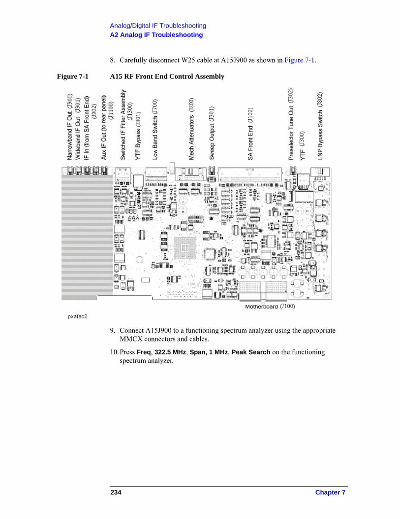
Analog/Digital IF Troubleshooting
A2 Analog IF Troubleshooting
8. Carefully disconnect W25 cable at A15J900 as shown in Figure 7-1.
Figure 7-1 A15 RF Front End Control Assembly
9. Connect A15J900 to a functioning spectrum analyzer using the appropriate MMCX connectors and cables.
10.Press Freq, 322.5 MHz, Span, 1 MHz, Peak Search on the functioning spectrum analyzer.
234 Chapter 7
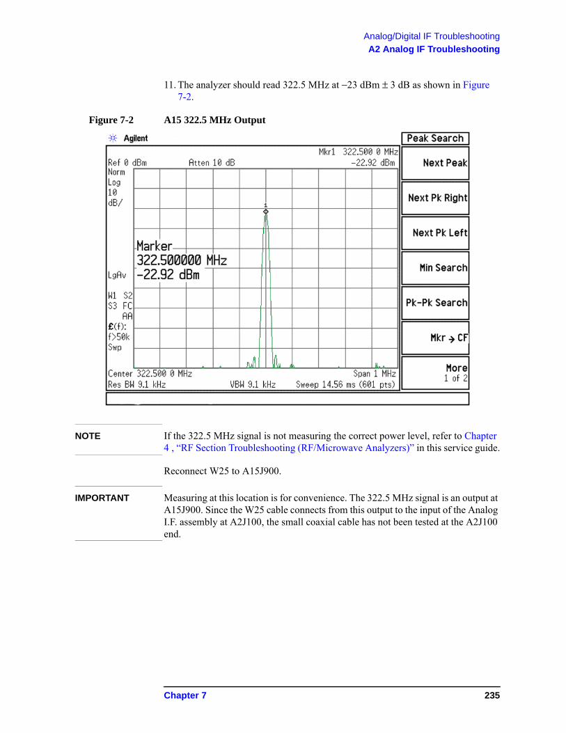
Analog/Digital IF Troubleshooting
A2 Analog IF Troubleshooting
11. The analyzer should read 322.5 MHz at −23 dBm ± 3 dB as shown in Figure 7-2.
Figure 7-2 A15 322.5 MHz Output
NOTE If the 322.5 MHz signal is not measuring the correct power level, refer to Chapter 4 , “RF Section Troubleshooting (RF/Microwave Analyzers)” in this service guide.
Reconnect W25 to A15J900.
IMPORTANT Measuring at this location is for convenience. The 322.5 MHz signal is an output at A15J900. Since the W25 cable connects from this output to the input of the Analog I.F. assembly at A2J100, the small coaxial cable has not been tested at the A2J100 end.
Chapter 7 235
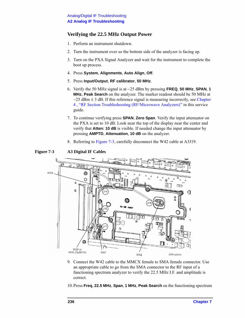
Analog/Digital IF Troubleshooting
A2 Analog IF Troubleshooting
Verifying the 22.5 MHz Output Power
1. Perform an instrument shutdown.
2. Turn the instrument over so the bottom side of the analyzer is facing up.
3. Turn on the PXA Signal Analyzer and wait for the instrument to complete the boot up process.
4. Press System, Alignments, Auto Align, Off.
5. Press Input/Output, RF calibrator, 50 MHz.
6. Verify the 50 MHz signal is at −25 dBm by pressing FREQ, 50 MHz, SPAN, 1 MHz, Peak Search on the analyzer. The marker readout should be 50 MHz at −25 dBm ± 3 dB. If this reference signal is measuring incorrectly, see Chapter 4 , “RF Section Troubleshooting (RF/Microwave Analyzers)” in this service guide.
7. To continue verifying press SPAN, Zero Span. Verify the input attenuator on the PXA is set to 10 dB. Look near the top of the display near the center and verify that Atten: 10 dB is visible. If needed change the input attenuator by pressing AMPTD, Attenuation, 10 dB on the analyzer.
8. Referring to Figure 7-3, carefully disconnect the W42 cable at A3J19.
Figure 7-3 A3 Digital IF Cables
9. Connect the W42 cable to the MMCX female to SMA female connector. Use an appropriate cable to go from the SMA connector to the RF input of a functioning spectrum analyzer to verify the 22.5 MHz I.F. and amplitude is correct.
10.Press Freq, 22.5 MHz, Span, 1 MHz, Peak Search on the functioning spectrum
236 Chapter 7
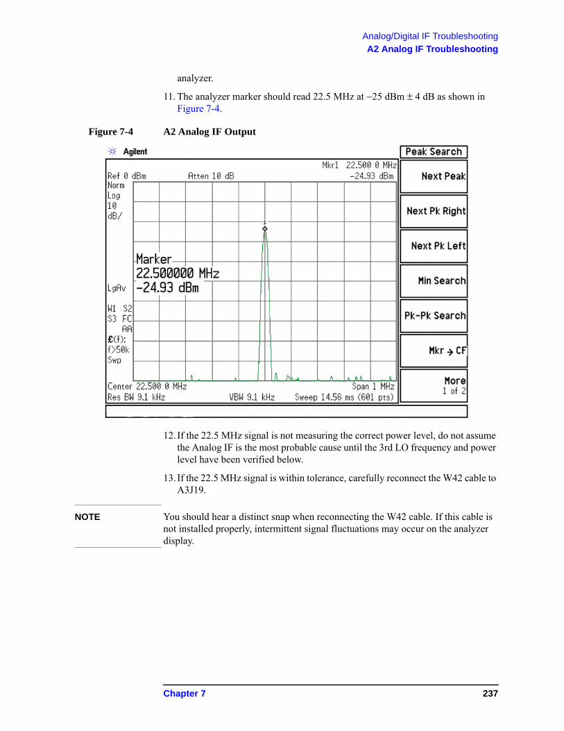
Analog/Digital IF Troubleshooting
A2 Analog IF Troubleshooting
analyzer.
11. The analyzer marker should read 22.5 MHz at −25 dBm ± 4 dB as shown in Figure 7-4.
Figure 7-4 A2 Analog IF Output
12. If the 22.5 MHz signal is not measuring the correct power level, do not assume the Analog IF is the most probable cause until the 3rd LO frequency and power level have been verified below.
13. If the 22.5 MHz signal is within tolerance, carefully reconnect the W42 cable to A3J19.
NOTE You should hear a distinct snap when reconnecting the W42 cable. If this cable is not installed properly, intermittent signal fluctuations may occur on the analyzer display.
Chapter 7 237
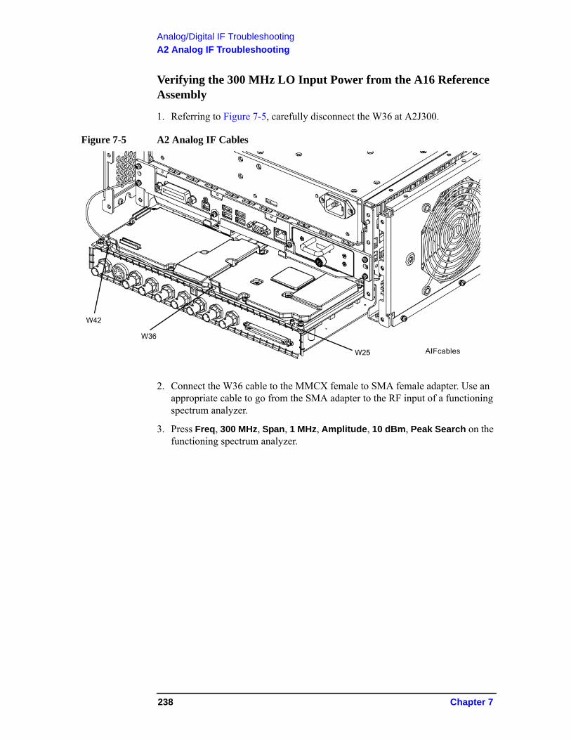
Analog/Digital IF Troubleshooting
A2 Analog IF Troubleshooting
Verifying the 300 MHz LO Input Power from the A16 Reference Assembly
1. Referring to Figure 7-5, carefully disconnect the W36 at A2J300.
Figure 7-5 A2 Analog IF Cables
2. Connect the W36 cable to the MMCX female to SMA female adapter. Use an appropriate cable to go from the SMA adapter to the RF input of a functioning spectrum analyzer.
3. Press Freq, 300 MHz, Span, 1 MHz, Amplitude, 10 dBm, Peak Search on the functioning spectrum analyzer.
238 Chapter 7
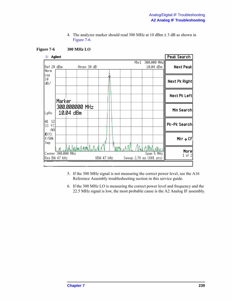
Analog/Digital IF Troubleshooting
A2 Analog IF Troubleshooting
4. The analyzer marker should read 300 MHz at 10 dBm ± 3 dB as shown in Figure 7-6.
Figure 7-6 300 MHz LO
5. If the 300 MHz signal is not measuring the correct power level, see the A16 Reference Assembly troubleshooting section in this service guide.
6. If the 300 MHz LO is measuring the correct power level and frequency and the 22.5 MHz signal is low, the most probable cause is the A2 Analog IF assembly.
Chapter 7 239
Analog/Digital IF Troubleshooting
A3 Digital IF Assembly Description
A3 Digital IF Assembly Description
The A3 Digital I.F. has circuitry that is needed to analyze complex communication signals that can occupy up to 40 MHz of information bandwidth. This assembly has two inputs:
1. The final 22.5 MHz I.F. from the A2 Analog I.F. for IF bandwidth paths up to 25 MHz wide. This input is used for swept and FFT spectrum analysis.
2. The 250 MHz IF from the A15 Front End Control Assembly for IF bandwidth of 40 MHz.
Each input has a separate ADC that processes the time domain continuous data into I/Q (in-phase and quadrature) signals before sending the data to the A4 CPU assembly for further processing and front panel display.
The Digital I.F. has the following main functions:
• Digitizes the 22.5 MHz and the 250 MHz IF signals
— 16 bit ADC with a 100 MHz sample rate to digitize the 22.5 MHz IF
— 12 bit ADC with a 200 MHz sample rate to digitize the 250 MHz IF
• DSP for standard spectrum analysis
• Capture memory for complex signals
• Noise Source Control
• Dither for final I.F
• Provides the alignment sequence generator for wide band alignments
• Provides wide band Comb Calibration Signal
• Trigger interpolation and associated alignment
240 Chapter 7
Analog/Digital IF Troubleshooting
A3 Digital IF Assembly Theory of Operation
A3 Digital IF Assembly Theory of Operation
NOTE Refer to Chapter 13 , “Block Diagrams”.
Data Acquisition
The 22.5 MHz IF comes from the A2 Analog IF assembly. The input level to the A3 Digital IF assembly is −25 dBm when observing the 50 MHz calibrator signal. The IF input has a 25 MHz bandwidth centered at 22.5 MHz. The analog circuitry leading to the ADC converts the singled ended signal from the Analog IF to differential required by the ADC. In addition, it is part of a filter, part of which is on the AIF, which improves distortion. Finally, it couples in the dither signal. The ADC is a 16 bit device sampling continuously at 100 Ms/second.
The 250 MHz IF comes from the A15 Front End Control assembly. The input level is approximately -25 dBm when observing the 50 MHz calibrator signal. The IF input has a 40 MHz bandwidth centered at 250 MHz. The analog circuitry leading to the ADC converts the single-ended signal from the Front End Control to differential required by the ADC. Finally, it couples in the dither signal. The ADC is a 12-bit device sampling continuously at 200 Ms/second.
Rear Panel Triggers
The board has two trigger inputs and two trigger outputs all used via BNC connectors on the rear panel. The trigger inputs are used when an external device has a trigger signal and the user wants to use that external trigger to trigger the signal analyzer. The trigger outputs are used to synchronize other pieces of test equipment to the PXA. These outputs are configurable through the Input/Output menu via the front panel of the instrument.
The trigger inputs each allow trigger levels to be set from −5 to +5 volts using the control DAC. The circuits have relatively high input impedance. The trigger outputs have 50 Ω source impedance with TTL drive levels into no load.
Control DAC
The control DAC is used to set trigger levels and the gain of the reconstruction system. All three outputs can be adjusted from −2.5 to +2.5 volts.
Sample Rate Generator
The 10 MHz reference signal comes from the A16 Reference Assembly. This signal is fairly high power at +10 dBm. The signal goes through a 10 MHz to 30 MHz tripler. A 0 to 5V, 10 MHz square wave is generated. Capacitors form a single-pole band pass filter to select the 3rd harmonic, 30 MHz.
The signal then passes through a 30 MHz to 90 MHz tripler. A 0 to 5V, 30 MHz square wave is generated. Capacitors form a single-pole band pass filter to select the 3rd harmonic, 90 MHz.
Chapter 7 241
Analog/Digital IF Troubleshooting
A3 Digital IF Assembly Theory of Operation
Noise Source Voltage Regulator
Various external noise sources can be connected to the rear panel of the PXA Signal Analyzer. These noise sources require a very accurate 28 volt DC power supply.
The 28 volt BNC output connector is used with the 346 series noise sources.
The Smart Noise Source (SNS) interface includes power switching for the 28 volt and 15 volt power supply. In addition, it has buffers to interface to the SNS I2C bus for control and read back of ENR data automatically. The SNS connector is used with the SNS series noise sources.
DSP
The signal from the ADC is sent to the Digital Signal Processor.
Digital Bus Common Mode Filtering
The Digital Bus is a real time digital interface. It is sometimes referred to as Messenger or LVDS. The implementation on the Digital IF is unidirectional, meaning it can only source data, not receive it. Common mode filtering is required to translate the digital ground referenced signals to analog ground at the rear panel.
242 Chapter 7
Analog/Digital IF Troubleshooting
A3 Digital IF Troubleshooting
A3 Digital IF Troubleshooting
Verifying the 22.5 MHz Input Power
1. Perform an instrument shutdown.
2. Remove the cover of the PXA Signal Analyzer. Refer to Chapter 16, “Assembly Replacement Procedures,” on page 427 in this service guide.
3. Turn the instrument over so that the bottom side of the analyzer is facing up.
4. Turn on the PXA Signal Analyzer and wait for the instrument to complete the boot up process.
5. Press System, Alignments, Auto Align, Off
6. Press Input/Output, RF Calibrator, 50 MHz
7. Verify the 50 MHz signal is at −25 dBm by pressing FREQ, 50 MHz, SPAN, 1 MHz, Peak Search on the analyzer. The marker readout should be 50 MHz at −25 dBm ± 3 dB. If this reference signal is measuring incorrectly, see Chapter 4 , “RF Section Troubleshooting (RF/Microwave Analyzers),” on page 147 in this service guide.
8. To continue verifying press SPAN, Zero Span. Verify the input attenuator on the PXA is set to 10 dB. Look near the top of the display near the center and verify Atten: 10 dB is visible. If needed change the input attenuator by pressing AMPTD, Attenuation, 10 dB on the analyzer.
Chapter 7 243
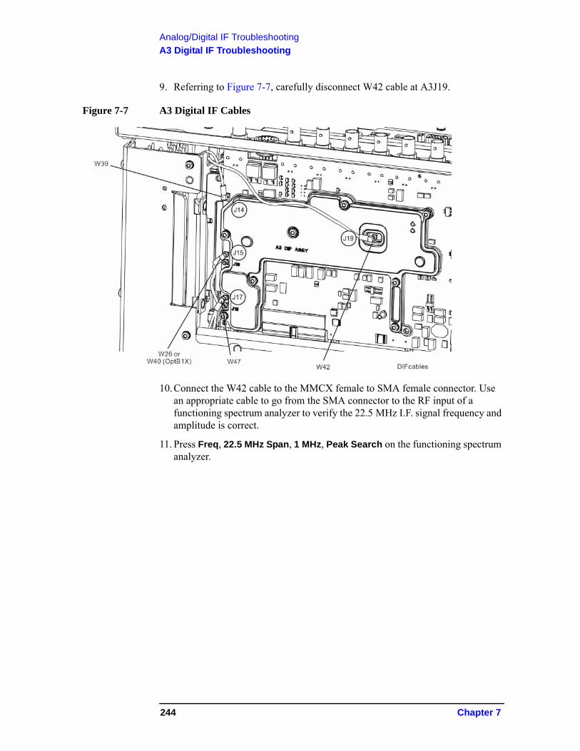
Analog/Digital IF Troubleshooting
A3 Digital IF Troubleshooting
9. Referring to Figure 7-7, carefully disconnect W42 cable at A3J19.
Figure 7-7 A3 Digital IF Cables
10.Connect the W42 cable to the MMCX female to SMA female connector. Use an appropriate cable to go from the SMA connector to the RF input of a functioning spectrum analyzer to verify the 22.5 MHz I.F. signal frequency and amplitude is correct.
11. Press Freq, 22.5 MHz Span, 1 MHz, Peak Search on the functioning spectrum analyzer.
244 Chapter 7
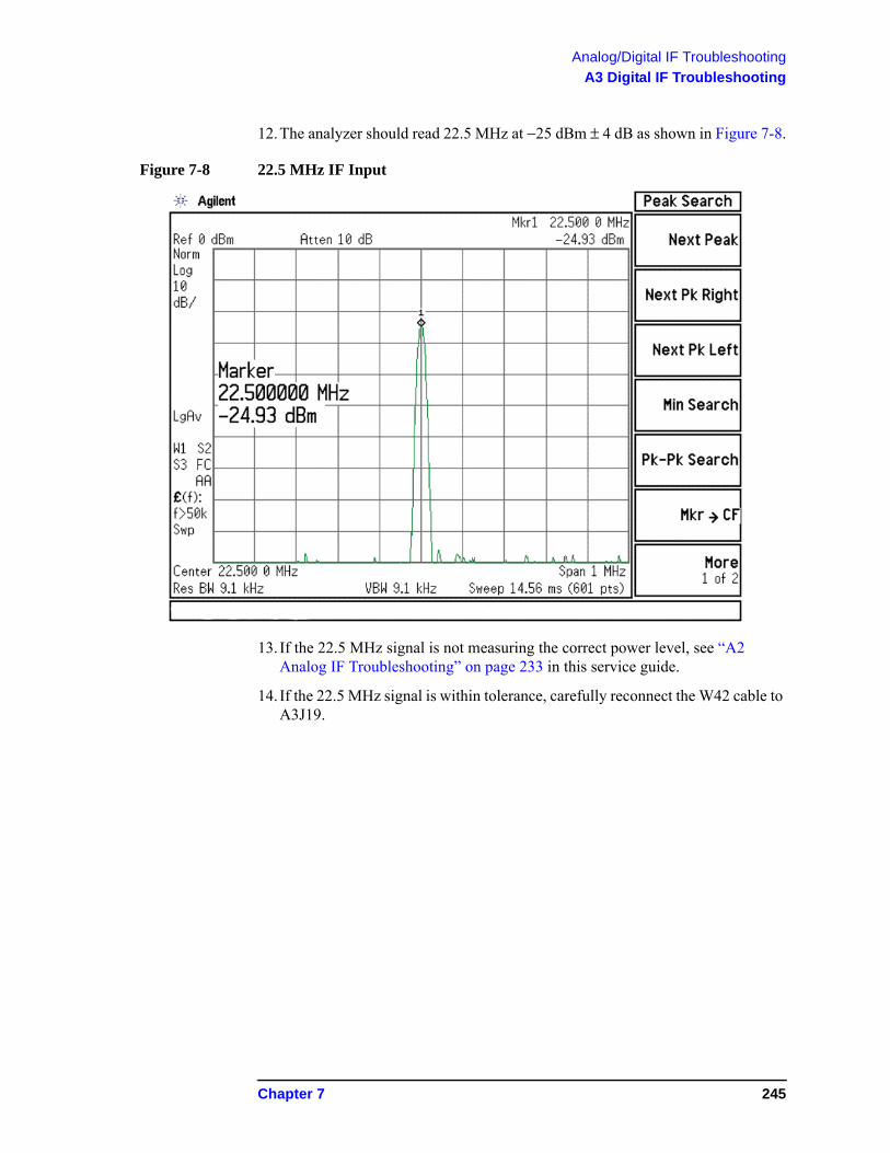
Analog/Digital IF Troubleshooting
A3 Digital IF Troubleshooting
12.The analyzer should read 22.5 MHz at −25 dBm ± 4 dB as shown in Figure 7-8.
Figure 7-8 22.5 MHz IF Input
13. If the 22.5 MHz signal is not measuring the correct power level, see “A2 Analog IF Troubleshooting” on page 233 in this service guide.
14. If the 22.5 MHz signal is within tolerance, carefully reconnect the W42 cable to A3J19.
Chapter 7 245
Analog/Digital IF Troubleshooting
A3 Digital IF Troubleshooting
Verifying the 250 MHz IF Input Power (Option B40 only)
NOTE Perform this procedure only if the analyzer is equipped with Option B40, Analysis Bandwidth, 40 MHz
1. Perform an instrument shutdown.
2. Remove the cover of the PXA Signal Analyzer. Refer to Chapter 16, “Assembly Replacement Procedures,” on page 427 in this service guide.
3. Turn the instrument over so that the bottom side of the analyzer is facing up.
4. Turn on the PXA Signal Analyzer and wait for the instrument to complete the boot up process.
5. Press Mode, IQ Analyzer (Basic), Mode Setup, IF Path, 40 MHz.
6. Press System, Alignments, Auto Align, Off.
7. Press Input/Output, RF calibrator, 50 MHz.
8. Verify the 50 MHz signal is at −25 dBm by pressing FREQ, 50 MHz, SPAN, 1 MHz, Peak Search on the analyzer. The maker readout should be 50 MHz at −25 dBm ± 3 dB. If this reference signal is measuring incorrectly, see Chapter 4 , “RF Section Troubleshooting (RF/Microwave Analyzers),” on page 147 in this service guide.
9. To continue verifying press Meas, IQ Waveform. Verify the input attenuator on the PXA is set to 10 dB. Look near the top of the display near the center and verify Atten: 10 dB is visible. If needed change the input attenuator by pressing AMPTD, Attenuation, 10 dB on the analyzer
10.Referring to Figure 7-11, carefully disconnect W26 or W40 (if analyzer is also equipped with Opt B1X) from A3J15.
246 Chapter 7
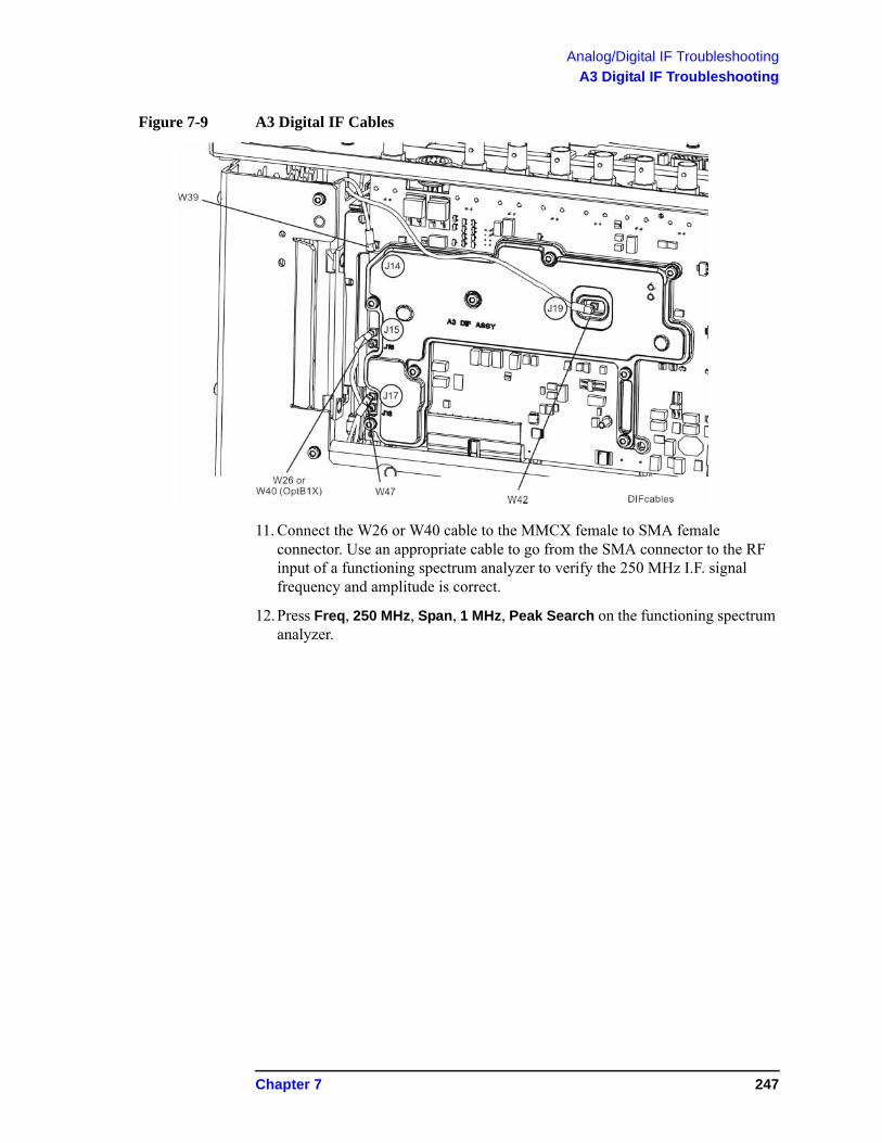
Analog/Digital IF Troubleshooting
A3 Digital IF Troubleshooting
Figure 7-9 A3 Digital IF Cables
11. Connect the W26 or W40 cable to the MMCX female to SMA female connector. Use an appropriate cable to go from the SMA connector to the RF input of a functioning spectrum analyzer to verify the 250 MHz I.F. signal frequency and amplitude is correct.
12.Press Freq, 250 MHz, Span, 1 MHz, Peak Search on the functioning spectrum analyzer.
Chapter 7 247
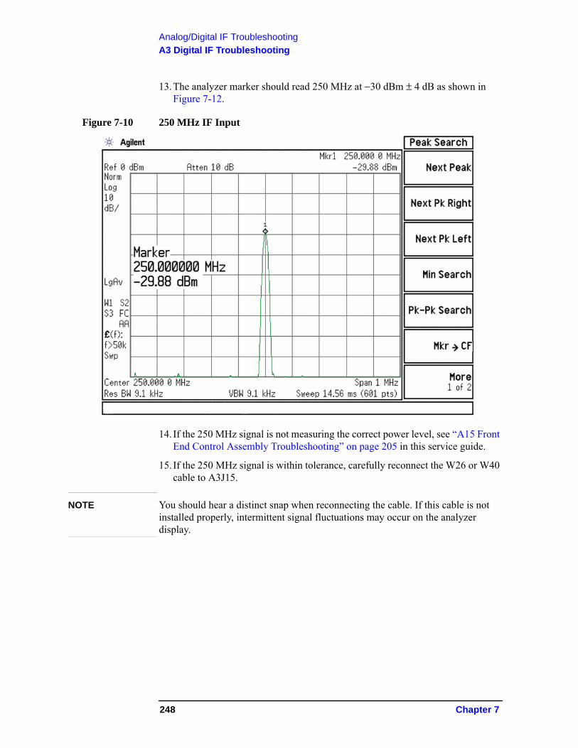
Analog/Digital IF Troubleshooting
A3 Digital IF Troubleshooting
13.The analyzer marker should read 250 MHz at −30 dBm ± 4 dB as shown in Figure 7-12.
Figure 7-10 250 MHz IF Input
14. If the 250 MHz signal is not measuring the correct power level, see “A15 Front End Control Assembly Troubleshooting” on page 205 in this service guide.
15. If the 250 MHz signal is within tolerance, carefully reconnect the W26 or W40 cable to A3J15.
NOTE You should hear a distinct snap when reconnecting the cable. If this cable is not installed properly, intermittent signal fluctuations may occur on the analyzer display.
248 Chapter 7
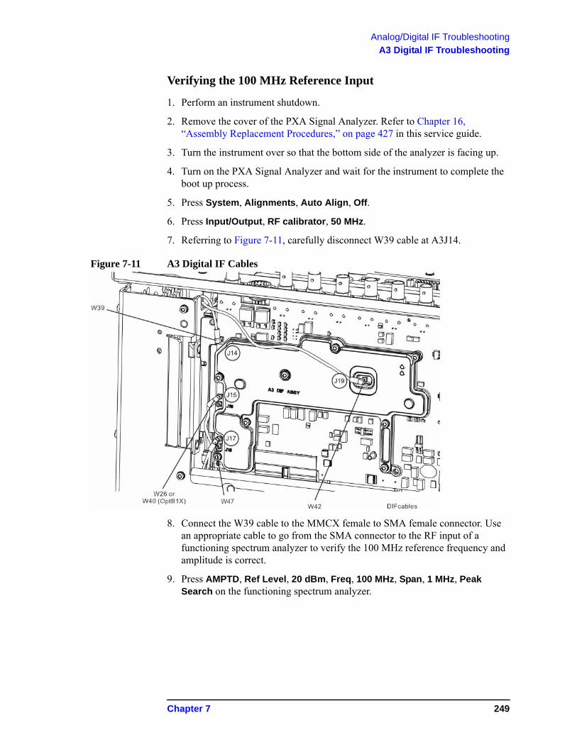
Analog/Digital IF Troubleshooting
A3 Digital IF Troubleshooting
Verifying the 100 MHz Reference Input
1. Perform an instrument shutdown.
2. Remove the cover of the PXA Signal Analyzer. Refer to Chapter 16, “Assembly Replacement Procedures,” on page 427 in this service guide.
3. Turn the instrument over so that the bottom side of the analyzer is facing up.
4. Turn on the PXA Signal Analyzer and wait for the instrument to complete the boot up process.
5. Press System, Alignments, Auto Align, Off.
6. Press Input/Output, RF calibrator, 50 MHz.
7. Referring to Figure 7-11, carefully disconnect W39 cable at A3J14.
Figure 7-11 A3 Digital IF Cables
8. Connect the W39 cable to the MMCX female to SMA female connector. Use an appropriate cable to go from the SMA connector to the RF input of a functioning spectrum analyzer to verify the 100 MHz reference frequency and amplitude is correct.
9. Press AMPTD, Ref Level, 20 dBm, Freq, 100 MHz, Span, 1 MHz, Peak Search on the functioning spectrum analyzer.
Chapter 7 249
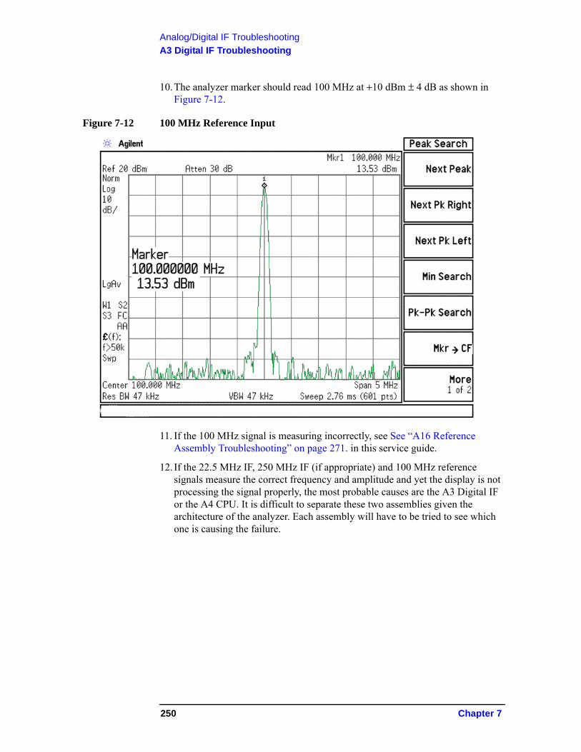
Analog/Digital IF Troubleshooting
A3 Digital IF Troubleshooting
10.The analyzer marker should read 100 MHz at +10 dBm ± 4 dB as shown in Figure 7-12.
Figure 7-12 100 MHz Reference Input
11. If the 100 MHz signal is measuring incorrectly, see See “A16 Reference Assembly Troubleshooting” on page 271. in this service guide.
12. If the 22.5 MHz IF, 250 MHz IF (if appropriate) and 100 MHz reference signals measure the correct frequency and amplitude and yet the display is not processing the signal properly, the most probable causes are the A3 Digital IF or the A4 CPU. It is difficult to separate these two assemblies given the architecture of the analyzer. Each assembly will have to be tried to see which one is causing the failure.
250 Chapter 7

8 LO Synthesizer/Reference Troubleshooting
251
LO Synthesizer/Reference Troubleshooting
What You Will Find in This Chapter
What You Will Find in This Chapter
The following information is presented in this chapter:
1. Theory of operation of the LO Synthesizer/Reference section.2. Isolating the cause of a hardware problem by verifying the functionality of
assemblies in the LO Synthesizer and Reference sections.
NOTE Each of the following sections first describes how the assembly works, then gives information to help you troubleshoot the assembly. Each description explains the purpose of the assembly, describes the main components, and lists external connections to the assembly.
The following information is found in this chapter:
A14 LO Synthesizer Assembly Description on page 253
A14 LO Synthesizer Theory of Operation on page 254
A14 LO Synthesizer and A20 YTO Troubleshooting on page 257
A16 Reference Assembly Description on page 269
A16 Reference Assembly Troubleshooting on page 271
252 Chapter 8
LO Synthesizer/Reference Troubleshooting
A14 LO Synthesizer Assembly Description
A14 LO Synthesizer Assembly Description
Purpose
The L.O. Synthesizer assembly provides the power and drive to the A20 YTO (YIG Tuned Oscillator). The A20 YTO is used as the 1st Local Oscillator (1st LO) in the A13A1 Front End Assembly for RF conversion. The A13A1 Front End distributes the 1st LO to the various mixers and to the A14 LO Synthesizer for purposes of phase locking the 1st LO. The frequency range of the 1st LO is 3.8 to 8.73 GHz.
The RF input signal mixes with the 1st L.O. in one of three possible mixers on the A13A1 Front End Assembly. For more detailed description on the Front End Assembly, see Chapter 4 , “RF Section Troubleshooting (RF/Microwave Analyzers)” in this service guide.
The A14 LO Synthesizer has the following inputs and outputs:
• Power Supply inputs
• Serial Bus input for LO Control
• Sweep input for LO Control
• 4800 MHz input signal from A16 Reference Assembly
• 100 MHz input signal from A16 Reference Assembly
• 1st LO output signal from A13 RF Front End Assembly
• Power and drive signals to the A20 YTO
The input signals to the LO Synthesizer Assembly are the 4800 MHz and 100 MHz reference signals from the A16 Reference Assembly. These signals are used to phase lock the offset loop on the A14 and the 1st LO. On the A16 Reference Assembly, both the 4800 MHz and 100 MHz reference signals are phase locked back to the 10 MHz reference, which is also located on A16.
The quality of the phase lock design that locks the 1st LO has a direct relationship on the overall stability of the analyzer. Users can also provide their own external reference. The frequency accuracy of the user's frequency reference is directly related to the overall frequency accuracy of the signal analyzer.
Chapter 8 253
LO Synthesizer/Reference Troubleshooting
A14 LO Synthesizer Theory of Operation
A14 LO Synthesizer Theory of Operation
NOTE Refer to Chapter 13 , “Block Diagrams”.
The LO Synthesizer can be operated in either dual-loop or single-loop modes. The dual-loop mode provides lower phase noise but slower tuning speed. The single-loop mode provides for fast tuning. The dual-loop mode is used for narrower spans, where phase noise impacts are the greatest, while single-loop mode is used in the wider spans, where tuning speed is most important.
The analyzer automatically chooses dual-loop mode for spans less than or equal to 10 MHz. This is the “customer span”, that is, the span annotated on the screen and visible to the customer. The LO span, which is the span to which the LO hardware is actually set, will be the customer span divided by N, the harmonic mixing number. The single-loop mode is automatically selected for customer spans wider than 10 MHz.
Single Loop Operation
In single-loop mode, the 100 MHz LO Synth reference signal from A16 is divided by two and the resulting 50 MHz signal is used as the reference input to the main loop phase/frequency detector. The 1st LO from A13A1J5, Synth Out, comes into A14J20 and its power is split two ways; one of the splitter outputs is used for dual-loop mode and the other output is used for single-loop mode.
In single-loop mode, the 1st LO signal is divided by two, yielding a range of 1.9 to 4.36 GHz and this divided signal is then fed to the fractional-N divider. The output of the fractional-N divider feeds the other input to the main loop phase/frequency detector. The output of the phase/frequency detector feeds the loop integrator which then drives the YTO Main and FM Coil Drivers.
There are also two types of single-loop modes; single-loop narrowband and single-loop wideband. The single-loop narrowband mode provides lower phase noise at offsets less than approximately 20 kHz.
Dual Loop Operation
In dual-loop mode, both the 100 MHz LO Synth and 4800 MHz 1st LO Reference signals are used. The 4800 MHz reference goes into a power splitter and one splitter output drives the fractional-N divider. The other output is used to drive a mixer in the Offset Loop synthesizer. The 100 MHz reference is split and one output used to drive a sampler in the Offset Loop synthesizer and the other output is divided by either 3 or 6 to yield a 16.6 or 33.3 MHz reference for the offset loop synthesizer.
The offset loop synthesizer is used to create a signal that is typically 33 to 55 MHz offset from the desired 1st LO frequency. To avoid generating synthesis related
254 Chapter 8
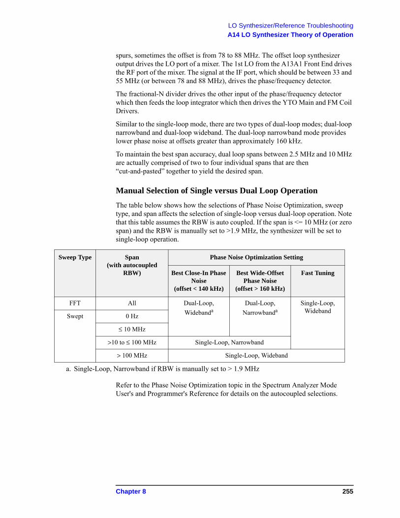
LO Synthesizer/Reference Troubleshooting
A14 LO Synthesizer Theory of Operation
spurs, sometimes the offset is from 78 to 88 MHz. The offset loop synthesizer output drives the LO port of a mixer. The 1st LO from the A13A1 Front End drives the RF port of the mixer. The signal at the IF port, which should be between 33 and 55 MHz (or between 78 and 88 MHz), drives the phase/frequency detector.
The fractional-N divider drives the other input of the phase/frequency detector which then feeds the loop integrator which then drives the YTO Main and FM Coil Drivers.
Similar to the single-loop mode, there are two types of dual-loop modes; dual-loop narrowband and dual-loop wideband. The dual-loop narrowband mode provides lower phase noise at offsets greater than approximately 160 kHz.
To maintain the best span accuracy, dual loop spans between 2.5 MHz and 10 MHz are actually comprised of two to four individual spans that are then “cut-and-pasted” together to yield the desired span.
Manual Selection of Single versus Dual Loop Operation
The table below shows how the selections of Phase Noise Optimization, sweep type, and span affects the selection of single-loop versus dual-loop operation. Note that this table assumes the RBW is auto coupled. If the span is <= 10 MHz (or zero span) and the RBW is manually set to >1.9 MHz, the synthesizer will be set to single-loop operation.
Refer to the Phase Noise Optimization topic in the Spectrum Analyzer Mode User's and Programmer's Reference for details on the autocoupled selections.
Sweep Type Span (with autocoupled
RBW)
Phase Noise Optimization Setting
Best Close-In Phase Noise
(offset < 140 kHz)
Best Wide-Offset Phase Noise
(offset > 160 kHz)
Fast Tuning
FFT All Dual-Loop,
WidebandaDual-Loop,
NarrowbandaSingle-Loop,
WidebandSwept 0 Hz
≤ 10 MHz
>10 to ≤ 100 MHz Single-Loop, Narrowband
> 100 MHz Single-Loop, Wideband
a. Single-Loop, Narrowband if RBW is manually set to > 1.9 MHz
Chapter 8 255
LO Synthesizer/Reference Troubleshooting
A14 LO Synthesizer Theory of Operation
Brief Description of the Major Blocks:
• The Field Programmable Gate Array (FPGA) L.O. Controller has the capability to pretune the A20 YTO, detect unlocks, and control the fractional-N divider, main loop, and offset loop.
• The Main Loop contains the fractional-N divider, phase/frequency detector, loop integrator, YTO Main and FM Coil drivers, the main loop mixer, and switches for selecting either single-loop or dual-loop operation. The input to the fractional-N divider is either the 4800 MHz reference (dual-loop) or the 1st LO signal divided by 2 (single-loop). The input to the phase frequency detector is either the 100 MHz reference divided by 2 (single-loop) or the IF of the main loop mixer (dual-loop).
• The Offset Loop is a very-low phase noise phase locked loop with coarse frequency settability. It is only used in dual-loop operation. Its output frequency is set to be typically 30 to 53 MHz above the desired 1st LO frequency, but the difference will sometimes be 78 to 88 MHz to avoid causing spurs The output of the offset loop is applied to the LO input of the main loop mixer, where it is mixed with the output of the A20 YTO.
• The reference frequency distribution consists of power splitters for each of the two reference signals (4800 MHz and 100 MHz) and a programmable divider for one splitter output of the 100 MHz reference signal. The programmable divider can be set to 2 to generate a 50 MHz reference for use in single-loop operation or to 3 or 6 to generate a 16.6 or 33.3 MHz reference for dual-loop operation.
256 Chapter 8
LO Synthesizer/Reference Troubleshooting
A14 LO Synthesizer and A20 YTO Troubleshooting
A14 LO Synthesizer and A20 YTO Troubleshooting
Turn on the N9030A Signal Analyzer and wait for the instrument to complete the boot up process. There are 8 processes to perform, which will verify the L.O. Synthesizer and YTO assemblies are functioning properly:
• Press Freq, 50 MHz, SPAN, Zero Span. LED's DS1 (yellow), DS2 (orange), and DS3 (red) located near the top of the board next to J9 should all be off. DS4 (green) should be on. See LED location in Figure 8-1 below. The definition of each LED is as follows:
— DS1 (yellow) When lit, indicates the analyzer is sweeping.
— DS2 (orange) When lit, indicates that the Offset Loop integrator exceeds its nominal range and is thus unlocked (applicable only in dual-loop mode).
— DS3 (red) When lit, means the Main Loop Cycle Slipped Detector has detected a cycle slipped condition and the main loop is thus unlocked.
It is normal for DS3 to flash between sweeps when the Main Loop is relocking. This can also occur during multiband sweeps. For example:
• sweeps which cross from one harmonic band to another such as from 2 GHz to 8 GHz.
• dual-loop spans between 2.5 MHz and 10 MHz.
— DS4 (green) When lit, indicates that the FPGA has been configured.
• Press System, Alignments, Align Now, All. If the alignment functions correctly with no error messages on the analyzer display, most of the synthesizer section is working properly.
• Measure 4800 MHz 1st LO Reference frequency (from A16 Reference Assembly)
• Measure 4800 MHz 1st LO Reference power (from A16 Reference Assembly)
• Measure 100 MHz LO Synth reference frequency (from A16 Reference Assembly)
• Measure 100 MHz LO Synth reference power (from A16 Reference Assembly)
• Measure 1st LO output frequency (from A20 YTO)
• Measure 1st LO output power (from A20 YTO)
These items can be checked with a functioning spectrum analyzer using cables and connectors that function well up to 10 GHz. A directional coupler, such as the 87300B, is also required for measuring the 1st LO output frequency and power.
Chapter 8 257
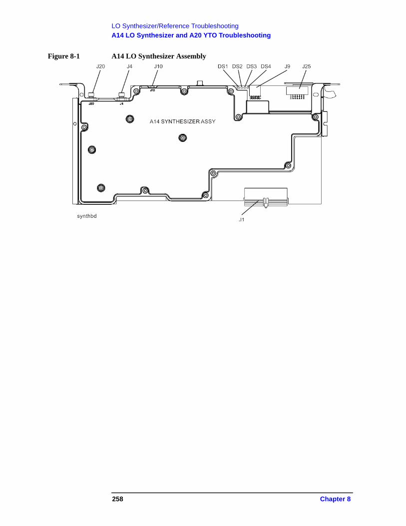
LO Synthesizer/Reference Troubleshooting
A14 LO Synthesizer and A20 YTO Troubleshooting
Figure 8-1 A14 LO Synthesizer Assembly
258 Chapter 8
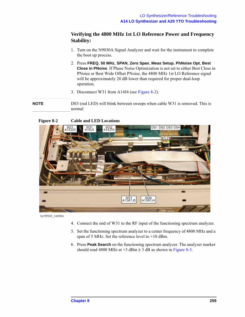
LO Synthesizer/Reference Troubleshooting
A14 LO Synthesizer and A20 YTO Troubleshooting
Verifying the 4800 MHz 1st LO Reference Power and Frequency Stability:
1. Turn on the N9030A Signal Analyzer and wait for the instrument to complete the boot up process.
2. Press FREQ, 50 MHz, SPAN, Zero Span, Meas Setup, PhNoise Opt, Best Close in PNoise. If Phase Noise Optimization is not set to either Best Close in PNoise or Best Wide Offset PNoise, the 4800 MHz 1st LO Reference signal will be approximately 20 dB lower than required for proper dual-loop operation.
3. Disconnect W31 from A14J4 (see Figure 8-2).
NOTE DS3 (red LED) will blink between sweeps when cable W31 is removed. This is normal
Figure 8-2 Cable and LED Locations
4. Connect the end of W31 to the RF input of the functioning spectrum analyzer.
5. Set the functioning spectrum analyzer to a center frequency of 4800 MHz and a span of 5 MHz. Set the reference level to +10 dBm.
6. Press Peak Search on the functioning spectrum analyzer. The analyzer marker should read 4800 MHz at +3 dBm ± 3 dB as shown in Figure 8-3.
Chapter 8 259
LO Synthesizer/Reference Troubleshooting
A14 LO Synthesizer and A20 YTO Troubleshooting
Figure 8-3 4800 MHz Wide Span
260 Chapter 8
LO Synthesizer/Reference Troubleshooting
A14 LO Synthesizer and A20 YTO Troubleshooting
7. Verify the 4800 MHz signal from the A16 Reference Assembly is stable by pressing SPAN, 50 kHz, BW, 1 kHz on the functioning spectrum analyzer. The signal on the functioning spectrum analyzer should be very stable both in frequency and power as shown in Figure 8-4.
8. Reconnect W31 A14J4.
Figure 8-4 4800 MHz Narrow Span
NOTE If the 4800 MHz signal is not measuring the correct power level, see the “A16 Reference Assembly Troubleshooting” section later in this chapter.
Chapter 8 261
LO Synthesizer/Reference Troubleshooting
A14 LO Synthesizer and A20 YTO Troubleshooting
Verifying the 100 MHz LO Synth Reference Power and Frequency Stability:
1. Turn on the N9030A Signal Analyzer and wait for the instrument to complete the boot up process.
2. Press FREQ, 50 MHz, SPAN, Zero Span.
3. Disconnect W32 from A14J10 (see Figure 8-5).
NOTE DS3 (red LED) will illuminate when cable W32 is removed. This is normal.
Figure 8-5 W32 Location
4. Connect the end of W32 to the RF input of the functioning spectrum analyzer.
5. Set the functioning spectrum analyzer to a center frequency of 100 MHz and a span of 5 MHz. Set the reference level to +20 dBm.
262 Chapter 8
LO Synthesizer/Reference Troubleshooting
A14 LO Synthesizer and A20 YTO Troubleshooting
6. Press Peak Search on the functioning spectrum analyzer. The analyzer marker should read 100 MHz at +13 dBm ±3 dB as shown in Figure 8-6.
Figure 8-6 100 MHz Wide Span
Chapter 8 263
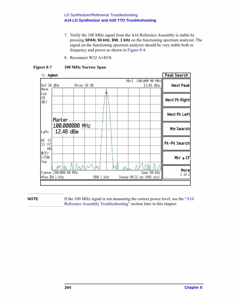
LO Synthesizer/Reference Troubleshooting
A14 LO Synthesizer and A20 YTO Troubleshooting
7. Verify the 100 MHz signal from the A16 Reference Assembly is stable by pressing SPAN, 50 kHz, BW, 1 kHz on the functioning spectrum analyzer. The signal on the functioning spectrum analyzer should be very stable both in frequency and power as shown in Figure 8-4.
8. Reconnect W32 A14J10.
Figure 8-7 100 MHz Narrow Span
NOTE If the 100 MHz signal is not measuring the correct power level, see the “A16 Reference Assembly Troubleshooting” section later in this chapter.
264 Chapter 8
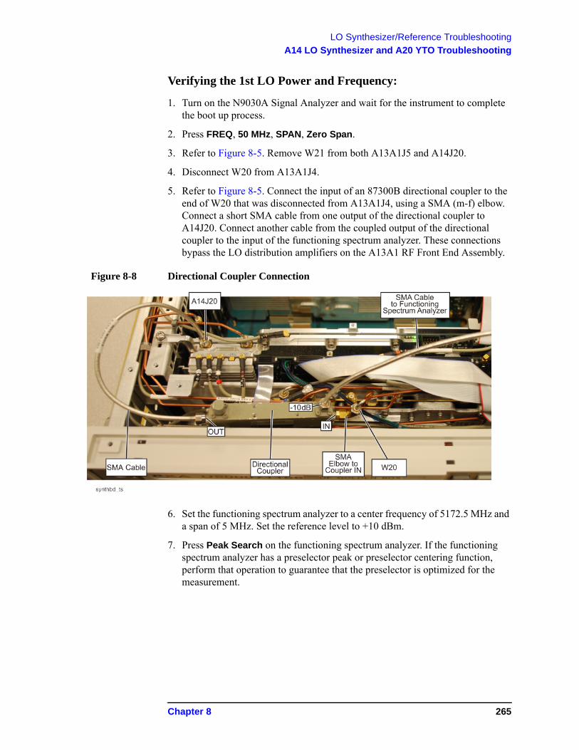
LO Synthesizer/Reference Troubleshooting
A14 LO Synthesizer and A20 YTO Troubleshooting
Verifying the 1st LO Power and Frequency:
1. Turn on the N9030A Signal Analyzer and wait for the instrument to complete the boot up process.
2. Press FREQ, 50 MHz, SPAN, Zero Span.
3. Refer to Figure 8-5. Remove W21 from both A13A1J5 and A14J20.
4. Disconnect W20 from A13A1J4.
5. Refer to Figure 8-5. Connect the input of an 87300B directional coupler to the end of W20 that was disconnected from A13A1J4, using a SMA (m-f) elbow. Connect a short SMA cable from one output of the directional coupler to A14J20. Connect another cable from the coupled output of the directional coupler to the input of the functioning spectrum analyzer. These connections bypass the LO distribution amplifiers on the A13A1 RF Front End Assembly.
Figure 8-8 Directional Coupler Connection
6. Set the functioning spectrum analyzer to a center frequency of 5172.5 MHz and a span of 5 MHz. Set the reference level to +10 dBm.
7. Press Peak Search on the functioning spectrum analyzer. If the functioning spectrum analyzer has a preselector peak or preselector centering function, perform that operation to guarantee that the preselector is optimized for the measurement.
Chapter 8 265
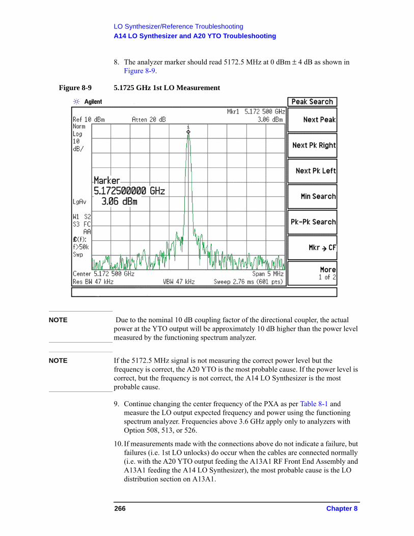
LO Synthesizer/Reference Troubleshooting
A14 LO Synthesizer and A20 YTO Troubleshooting
8. The analyzer marker should read 5172.5 MHz at 0 dBm ± 4 dB as shown in Figure 8-9.
Figure 8-9 5.1725 GHz 1st LO Measurement
NOTE Due to the nominal 10 dB coupling factor of the directional coupler, the actual power at the YTO output will be approximately 10 dB higher than the power level measured by the functioning spectrum analyzer.
NOTE If the 5172.5 MHz signal is not measuring the correct power level but the frequency is correct, the A20 YTO is the most probable cause. If the power level is correct, but the frequency is not correct, the A14 LO Synthesizer is the most probable cause.
9. Continue changing the center frequency of the PXA as per Table 8-1 and measure the LO output expected frequency and power using the functioning spectrum analyzer. Frequencies above 3.6 GHz apply only to analyzers with Option 508, 513, or 526.
10. If measurements made with the connections above do not indicate a failure, but failures (i.e. 1st LO unlocks) do occur when the cables are connected normally (i.e. with the A20 YTO output feeding the A13A1 RF Front End Assembly and A13A1 feeding the A14 LO Synthesizer), the most probable cause is the LO distribution section on A13A1.
266 Chapter 8
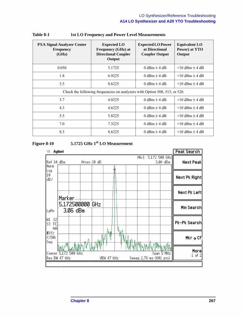
LO Synthesizer/Reference Troubleshooting
A14 LO Synthesizer and A20 YTO Troubleshooting
Figure 8-10 5.1725 GHz 1st LO Measurement
Table 8-1 1st LO Frequency and Power Level Measurements
PXA Signal Analyzer Center Frequency
(GHz)
Expected LO Frequency (GHz) at Directional Coupler
Output
Expected LO Power at Directional
Coupler Output
Equivalent LO Power) at YTO Output
0.050 5.1725 0 dBm ± 4 dB +10 dBm ± 4 dB
1.8 6.9225 0 dBm ± 4 dB +10 dBm ± 4 dB
3.5 8.6225 0 dBm ± 4 dB +10 dBm ± 4 dB
Check the following frequencies on analyzers with Option 508, 513, or 526
3.7 4.0225 0 dBm ± 4 dB +10 dBm ± 4 dB
4.3 4.6225 0 dBm ± 4 dB +10 dBm ± 4 dB
5.5 5.8225 0 dBm ± 4 dB +10 dBm ± 4 dB
7.0 7.3225 0 dBm ± 4 dB +10 dBm ± 4 dB
8.3 8.6225 0 dBm ± 4 dB +10 dBm ± 4 dB
Chapter 8 267
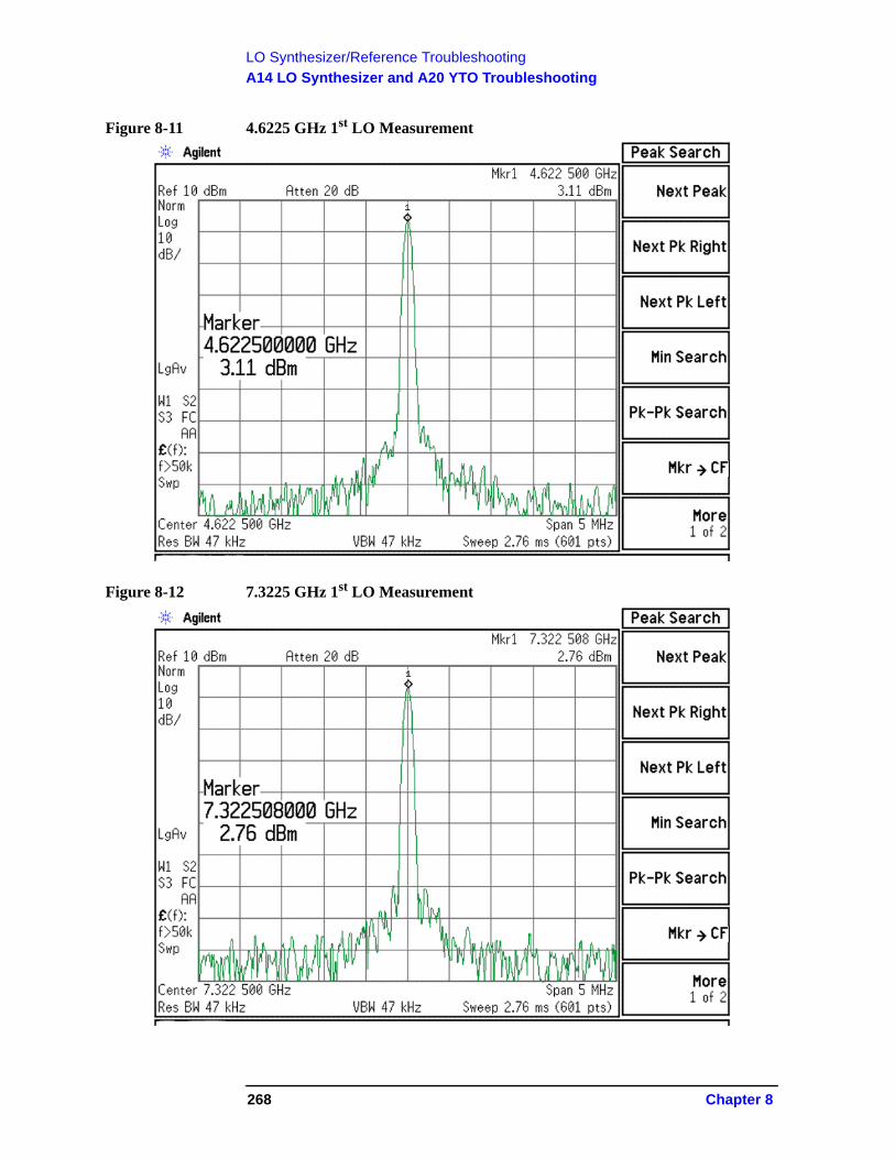
LO Synthesizer/Reference Troubleshooting
A14 LO Synthesizer and A20 YTO Troubleshooting
Figure 8-11 4.6225 GHz 1st LO Measurement
Figure 8-12 7.3225 GHz 1st LO Measurement
268 Chapter 8
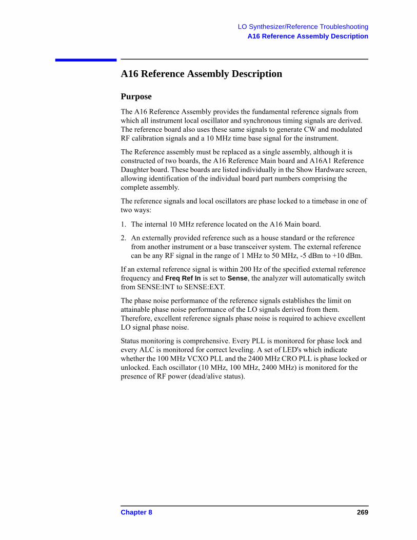
LO Synthesizer/Reference Troubleshooting
A16 Reference Assembly Description
A16 Reference Assembly Description
Purpose
The A16 Reference Assembly provides the fundamental reference signals from which all instrument local oscillator and synchronous timing signals are derived. The reference board also uses these same signals to generate CW and modulated RF calibration signals and a 10 MHz time base signal for the instrument.
The Reference assembly must be replaced as a single assembly, although it is constructed of two boards, the A16 Reference Main board and A16A1 Reference Daughter board. These boards are listed individually in the Show Hardware screen, allowing identification of the individual board part numbers comprising the complete assembly.
The reference signals and local oscillators are phase locked to a timebase in one of two ways:
1. The internal 10 MHz reference located on the A16 Main board.
2. An externally provided reference such as a house standard or the reference from another instrument or a base transceiver system. The external reference can be any RF signal in the range of 1 MHz to 50 MHz, -5 dBm to +10 dBm.
If an external reference signal is within 200 Hz of the specified external reference frequency and Freq Ref In is set to Sense, the analyzer will automatically switch from SENSE:INT to SENSE:EXT.
The phase noise performance of the reference signals establishes the limit on attainable phase noise performance of the LO signals derived from them. Therefore, excellent reference signals phase noise is required to achieve excellent LO signal phase noise.
Status monitoring is comprehensive. Every PLL is monitored for phase lock and every ALC is monitored for correct leveling. A set of LED's which indicate whether the 100 MHz VCXO PLL and the 2400 MHz CRO PLL is phase locked or unlocked. Each oscillator (10 MHz, 100 MHz, 2400 MHz) is monitored for the presence of RF power (dead/alive status).
Chapter 8 269
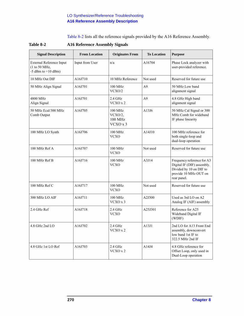
LO Synthesizer/Reference Troubleshooting
A16 Reference Assembly Description
Table 8-2 lists all the reference signals provided by the A16 Reference Assembly.
Table 8-2 A16 Reference Assembly Signals
Signal Description From Location Originates From To Location Purpose
External Reference Input (1 to 50 MHz, -5 dBm to +10 dBm)
Input from User n/a A16704 Phase Lock analyzer with user-provided reference.
10 MHz Out DIF A16J710 10 MHz Reference Not used Reserved for future use
50 MHz Align Signal A16J701 100 MHz VCXO/2
A9 50 MHz Low band alignment signal
4800 MHz Align Signal
A16J701 2.4 GHz VCXO x 2
A9 4.8 GHz High band alignment signal
50 MHz Ecal/300 MHz Comb Output
A16J705 100 MHz VCXO/2, 100 MHz VCXO x 3
A13J6 50 MHz Cal Signal or 300 MHz Comb for wideband IF phase linearity
100 MHz LO Synth A16J706 100 MHz VCXO
A14J10 100 MHz reference for both single-loop and dual-loop operation
100 MHz Ref A A16J707 100 MHz VCXO
Not used Reserved for future use
100 MHz Ref B A16J716 100 MHz VCXO
A3J14 Frequency reference for A3 Digital IF (DIF) assembly. Divided by 10 on DIF to provide 10 MHz OUT on rear panel.
100 MHz Ref C A16J717 100 MHz VCXO
Not used Reserved for future use
300 MHz LO AIF A16J711 100 MHz VCXO x 3
A2J300 Used as 3rd LO on A2 Analog IF (AIF) assembly
2.4 GHz Ref A16J718 2.4 GHz VCXO
A25J301 Reference for A25 Wideband Digital IF (WDIF)
4.8 GHz 2nd LO A16J702 2.4 GHz VCXO x 2
A13J1 2nd LO for A13 Front End assembly, downconvert low band 1st IF to 322.5 MHz 2nd IF
4.8 GHz 1st LO Ref A16J703 2.4 GHz VCXO x 2
A14J4 4.8 GHz reference for Offset Loop, only used in Dual-Loop operation
270 Chapter 8
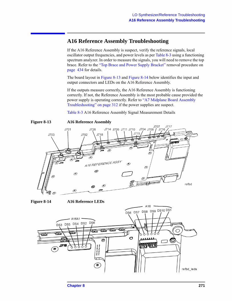
LO Synthesizer/Reference Troubleshooting
A16 Reference Assembly Troubleshooting
A16 Reference Assembly Troubleshooting
If the A16 Reference Assembly is suspect, verify the reference signals, local oscillator output frequencies, and power levels as per Table 8-3 using a functioning spectrum analyzer. In order to measure the signals, you will need to remove the top brace. Refer to the “Top Brace and Power Supply Bracket” removal procedure on page 434 for details.
The board layout in Figure 8-13 and Figure 8-14 below identifies the input and output connectors and LEDs on the A16 Reference Assembly.
If the outputs measure correctly, the A16 Reference Assembly is functioning correctly. If not, the Reference Assembly is the most probable cause provided the power supply is operating correctly. Refer to “A7 Midplane Board Assembly Troubleshooting” on page 312 if the power supplies are suspect.
Table 8-3 A16 Reference Assembly Signal Measurement Details
Figure 8-13 A16 Reference Assembly
Figure 8-14 A16 Reference LEDs
Chapter 8 271
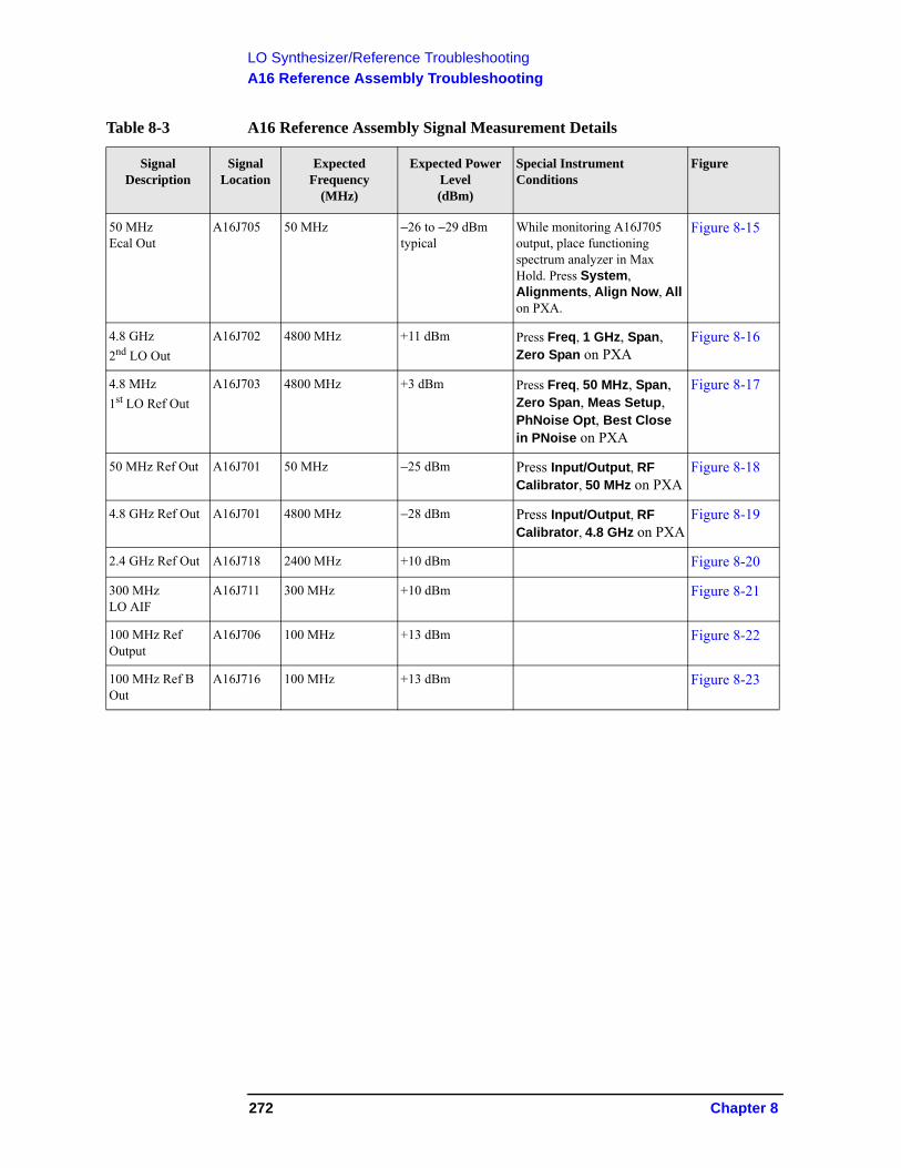
LO Synthesizer/Reference Troubleshooting
A16 Reference Assembly Troubleshooting
Table 8-3 A16 Reference Assembly Signal Measurement Details
Signal Description
Signal Location
Expected Frequency
(MHz)
Expected Power Level(dBm)
Special Instrument Conditions
Figure
50 MHz Ecal Out
A16J705 50 MHz −26 to −29 dBm typical
While monitoring A16J705 output, place functioning spectrum analyzer in Max Hold. Press System, Alignments, Align Now, All on PXA.
Figure 8-15
4.8 GHz
2nd LO Out
A16J702 4800 MHz +11 dBm Press Freq, 1 GHz, Span, Zero Span on PXA
Figure 8-16
4.8 MHz
1st LO Ref Out
A16J703 4800 MHz +3 dBm Press Freq, 50 MHz, Span, Zero Span, Meas Setup, PhNoise Opt, Best Close in PNoise on PXA
Figure 8-17
50 MHz Ref Out A16J701 50 MHz −25 dBm Press Input/Output, RF Calibrator, 50 MHz on PXA
Figure 8-18
4.8 GHz Ref Out A16J701 4800 MHz −28 dBm Press Input/Output, RF Calibrator, 4.8 GHz on PXA
Figure 8-19
2.4 GHz Ref Out A16J718 2400 MHz +10 dBm Figure 8-20
300 MHz LO AIF
A16J711 300 MHz +10 dBm Figure 8-21
100 MHz Ref Output
A16J706 100 MHz +13 dBm Figure 8-22
100 MHz Ref B Out
A16J716 100 MHz +13 dBm Figure 8-23
272 Chapter 8
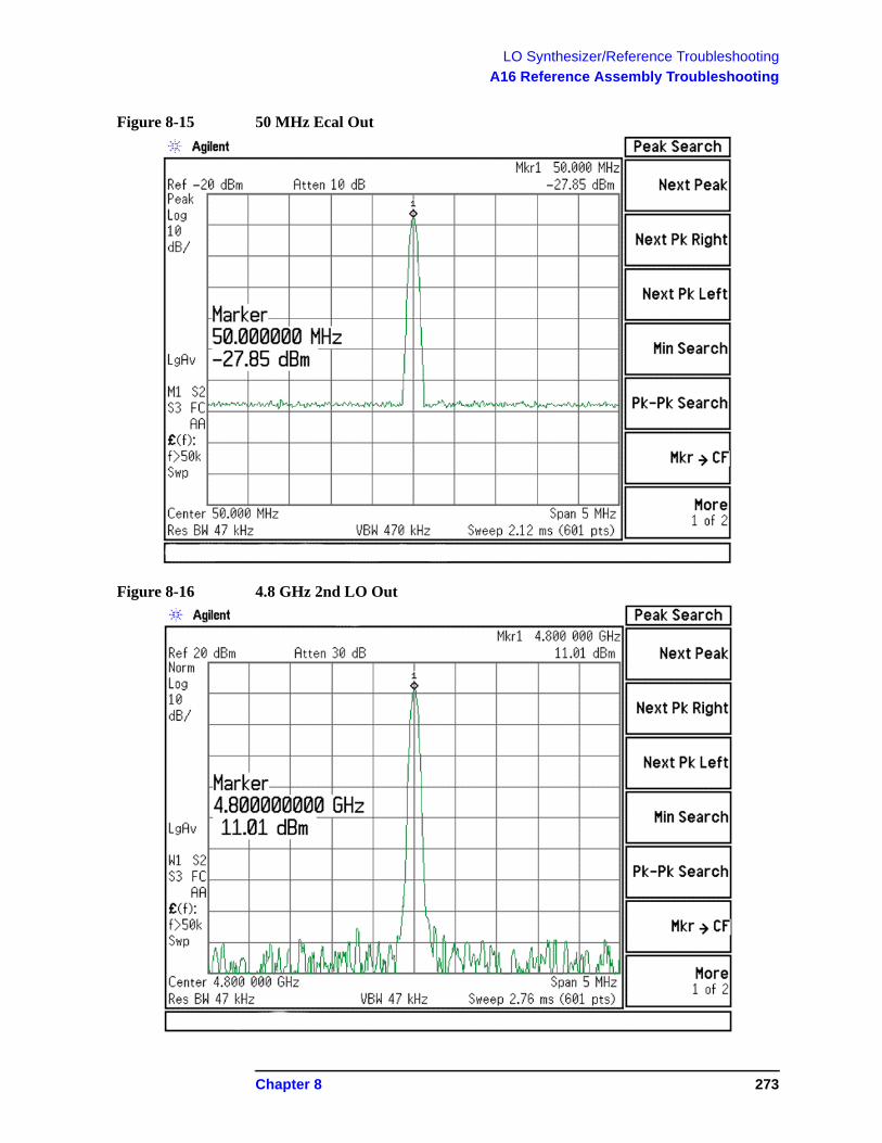
LO Synthesizer/Reference Troubleshooting
A16 Reference Assembly Troubleshooting
Figure 8-15 50 MHz Ecal Out
Figure 8-16 4.8 GHz 2nd LO Out
Chapter 8 273
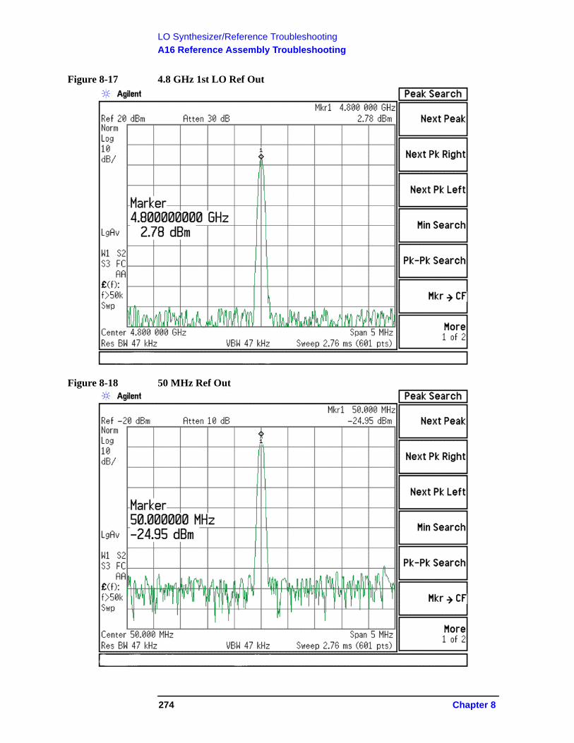
LO Synthesizer/Reference Troubleshooting
A16 Reference Assembly Troubleshooting
Figure 8-17 4.8 GHz 1st LO Ref Out
Figure 8-18 50 MHz Ref Out
274 Chapter 8
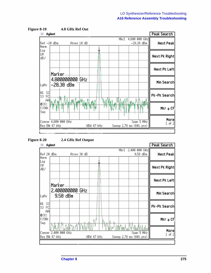
LO Synthesizer/Reference Troubleshooting
A16 Reference Assembly Troubleshooting
Figure 8-19 4.8 GHz Ref Out
Figure 8-20 2.4 GHz Ref Output
Chapter 8 275
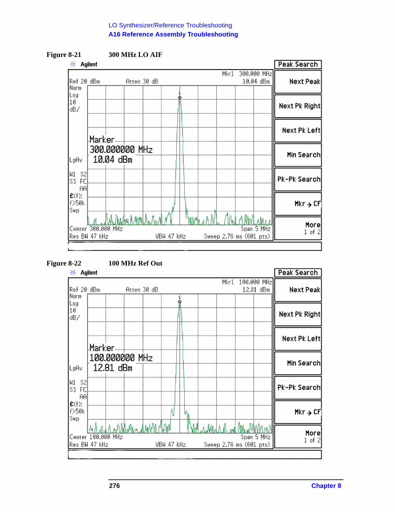
LO Synthesizer/Reference Troubleshooting
A16 Reference Assembly Troubleshooting
Figure 8-21 300 MHz LO AIF
Figure 8-22 100 MHz Ref Out
276 Chapter 8
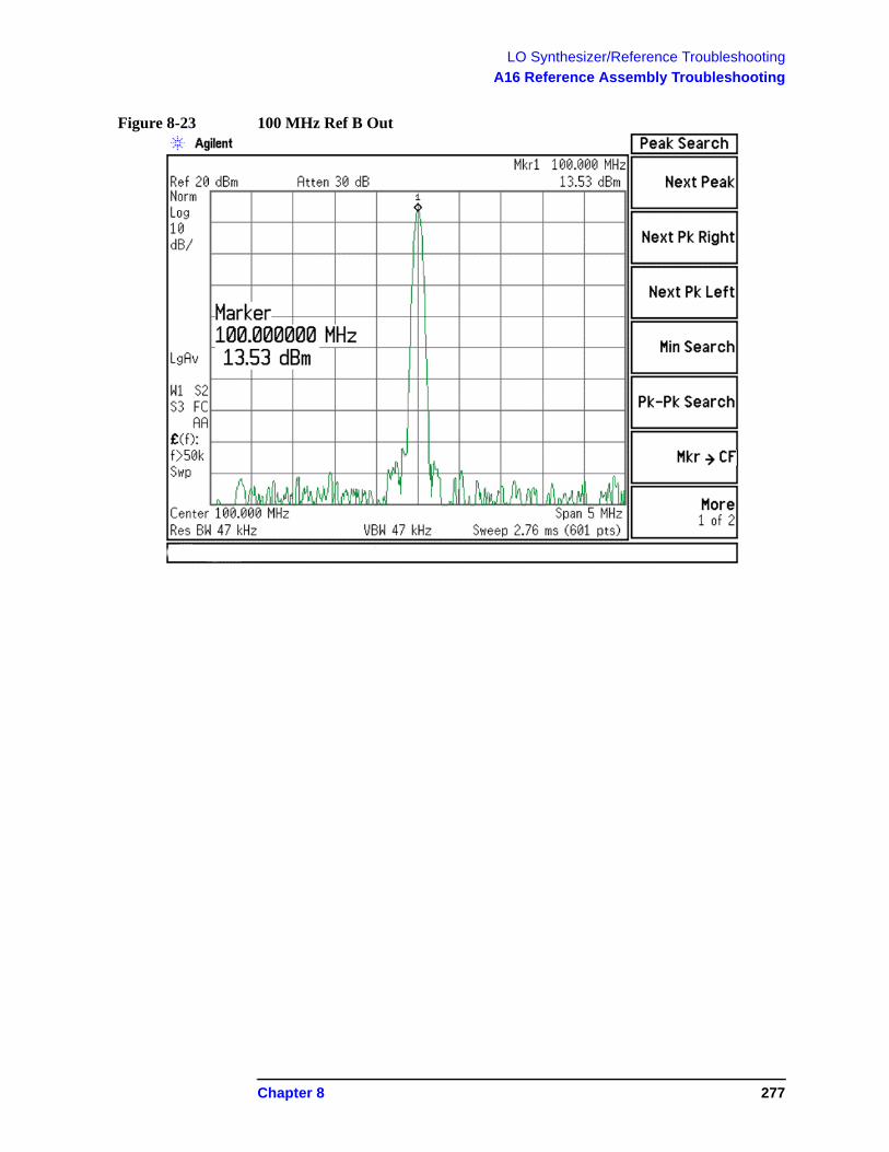
LO Synthesizer/Reference Troubleshooting
A16 Reference Assembly Troubleshooting
Figure 8-23 100 MHz Ref B Out
Chapter 8 277
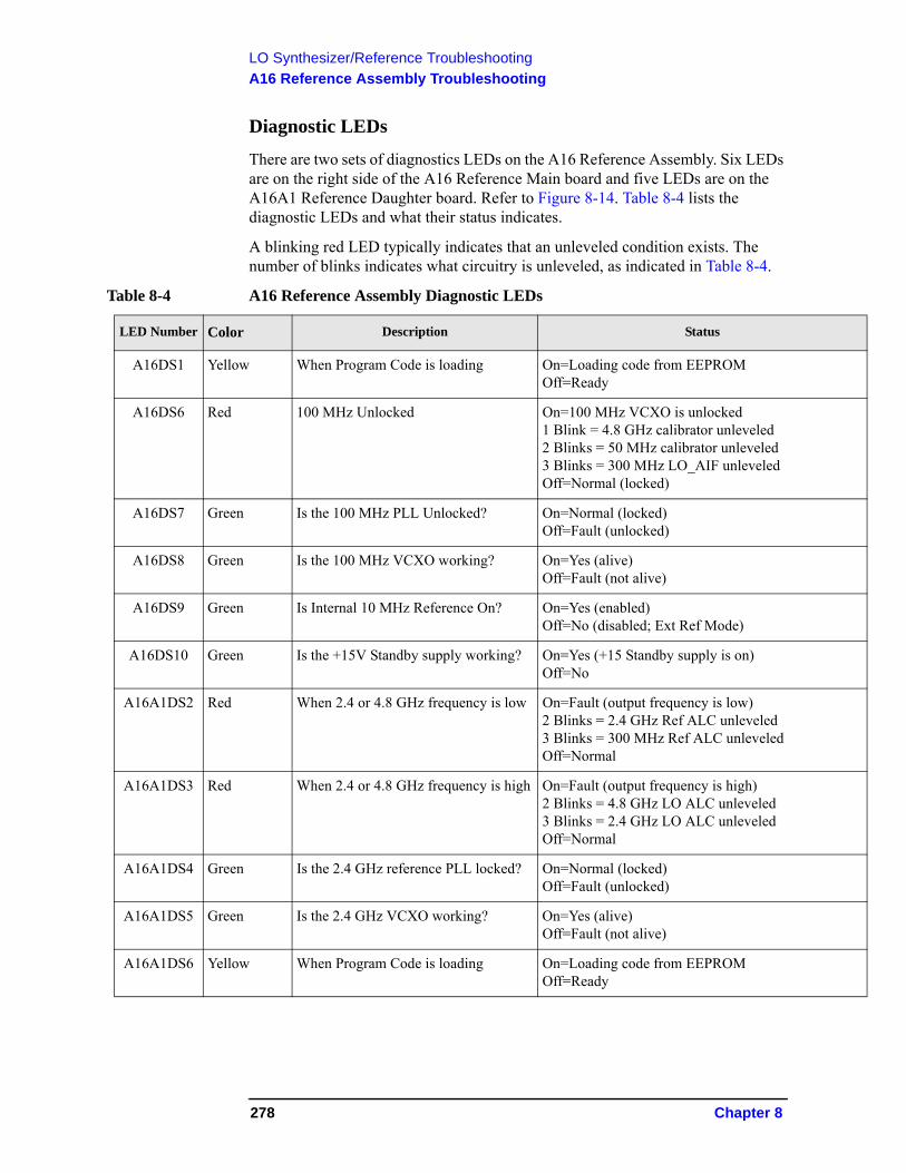
LO Synthesizer/Reference Troubleshooting
A16 Reference Assembly Troubleshooting
Diagnostic LEDs
There are two sets of diagnostics LEDs on the A16 Reference Assembly. Six LEDs are on the right side of the A16 Reference Main board and five LEDs are on the A16A1 Reference Daughter board. Refer to Figure 8-14. Table 8-4 lists the diagnostic LEDs and what their status indicates.
A blinking red LED typically indicates that an unleveled condition exists. The number of blinks indicates what circuitry is unleveled, as indicated in Table 8-4.
Table 8-4 A16 Reference Assembly Diagnostic LEDs
LED Number Color Description Status
A16DS1 Yellow When Program Code is loading On=Loading code from EEPROMOff=Ready
A16DS6 Red 100 MHz Unlocked On=100 MHz VCXO is unlocked1 Blink = 4.8 GHz calibrator unleveled2 Blinks = 50 MHz calibrator unleveled3 Blinks = 300 MHz LO_AIF unleveledOff=Normal (locked)
A16DS7 Green Is the 100 MHz PLL Unlocked? On=Normal (locked)Off=Fault (unlocked)
A16DS8 Green Is the 100 MHz VCXO working? On=Yes (alive)Off=Fault (not alive)
A16DS9 Green Is Internal 10 MHz Reference On? On=Yes (enabled)Off=No (disabled; Ext Ref Mode)
A16DS10 Green Is the +15V Standby supply working? On=Yes (+15 Standby supply is on)Off=No
A16A1DS2 Red When 2.4 or 4.8 GHz frequency is low On=Fault (output frequency is low)2 Blinks = 2.4 GHz Ref ALC unleveled3 Blinks = 300 MHz Ref ALC unleveledOff=Normal
A16A1DS3 Red When 2.4 or 4.8 GHz frequency is high On=Fault (output frequency is high)2 Blinks = 4.8 GHz LO ALC unleveled3 Blinks = 2.4 GHz LO ALC unleveledOff=Normal
A16A1DS4 Green Is the 2.4 GHz reference PLL locked? On=Normal (locked)Off=Fault (unlocked)
A16A1DS5 Green Is the 2.4 GHz VCXO working? On=Yes (alive)Off=Fault (not alive)
A16A1DS6 Yellow When Program Code is loading On=Loading code from EEPROMOff=Ready
278 Chapter 8
9 CPU/Disk Drive Troubleshooting
279
CPU/Disk Drive Troubleshooting
What You Will Find in This Chapter
What You Will Find in This Chapter
The following information is presented in this chapter:
1. Theory of operation of the CPU section.2. Isolating the cause of a hardware problem by verifying the functionality of
assemblies in the CPU section.
NOTE Each section first describes how the assembly works, then gives information to help you troubleshoot the assembly. Each description explains the purpose of the assembly, describes the main components, and lists external connections to the assembly.
This following sections are found in this chapter:
A4 CPU Description on page 281
A4 Processor Board Assembly Troubleshooting on page 283
A5 Disk Drive on page 294
Troubleshooting software related issues on page 296
Reloading the X-Series Software on page 297
Disk Drive Recovery Process on page 298
Replacing the instrument disk drive on page 300
280 Chapter 9
CPU/Disk Drive Troubleshooting
A4 CPU Description
A4 CPU Description
If the CPU board is suspect in an instrument failure, a full description of the instrument boot process is described in Chapter 2, “Boot Up and Initialization Troubleshooting”.
Disk Drive
The A5 Disk Drive can easily be removed from the A4 CPU assembly without removing instrument covers. The disk drive is attached to a tray that is accessed on the rear panel by loosening one screw and pulling the drive out of the CPU assembly. The disk drive mates with the CPU board via the A4A1 Disk Drive Interface Board. If the A4 CPU assembly is replaced, the existing A5 Disk Drive must be transferred to the replacement CPU assembly.
A4A1 Disk Drive Interface Board
The disk drive interface board plugs into a header on the A4 CPU, attaches with screws, and is separately replaceable. There may be situations where the disk drive must be removed and inserted many times such as in a security sensitive environment. Therefore, the low cost disk drive interface board can be replaced if connector wear is an issue.
Front Panel Interface
The instrument USB bus is the electrical interface to the instrument front panel. One of the USB ports on the host controller hub located on the A4 CPU board assembly is routed to the A1A2 Front Panel Interface board for this use. The port is a High Speed USB (2.0) compliant port.
Graphics Controller
The entire graphics subsystem is contained within a single chip, along with the interface logic to map memory from main system memory for the video RAM. There are two outputs of the graphics controller that are used by the instrument. One provides the LCD video data to drive the internal instrument LCD display and the other supplies the rear panel VGA output.
Power Supply Control
The power control line from the front panel momentary power switch connects to the A4 CPU board assembly. When the front panel power switch is turned on the A4 CPU board assembly pulls the PS_ON line to the A6 Power Supply assembly to a TTL low level, which tells the power supply to turn on. Once the +12V D, +5.1V D, and +3.35V D supplies are all on and within specification the A6 Power Supply assembly pulls the PWROK_H line to a TTL high state, which then causes the A4 CPU board to come out of reset and boot-up.
Chapter 9 281
CPU/Disk Drive Troubleshooting
A4 CPU Description
Outputs from the A4 CPU board assembly also drive the two front panel power state LEDs.
Provisions have also been made to allow the CPU board to remember which power state it was in when a power failure occurs. The instrument will return to the same power state after a power failure.
Rear Panel Connectivity
The A4 CPU board assembly has direct access to the rear panel of the instrument. The external connections provided on the A4 CPU board assembly include:
• External VGA• LAN (RJ45) 10/100/1000 based-T Ethernet port• USB
— 4 x Type-A ports (USB 2.0 compatible)— 1 x Type-B port (USB 2.0 compatible) Instrument behaves like a USB
device (client)
• GPIB
System Memory
The type and amount of system RAM in the instrument may vary depending on the age and options installed in an instrument.
Current instruments will have 4 GBytes of DDR SDRAM in two 200-pin SODIMM memory modules.
While the memory controller chips do support a wide range of DDR memory types, only memory fully qualified by Agilent Technologies is supported. Full qualification includes mechanical vibration and shock, thermal and power dissipation and the basic electrical characteristics.
The 200-pin SODIMM memory modules are not field replaceable.
All replacement A4 CPU board assemblies come with the appropriate memory modules installed.
System Processor
The A4 CPU board assembly uses an Intel Pentium-M series processor chip.
CPU Battery
The LI-ION battery powers the instrument clock and maintains the settings for the CMOS BIOS configuration. Agilent changes the boot order setting so the instrument disk drive is first. If the battery fails, the boot order reverts to the USB first. Therefore if a non-bootable USB device is connected when the instrument powers up, a black screen with a message such as: “Failure: No bootable partition in table” will result and may cause the user to believe the instrument is faulty.
282 Chapter 9
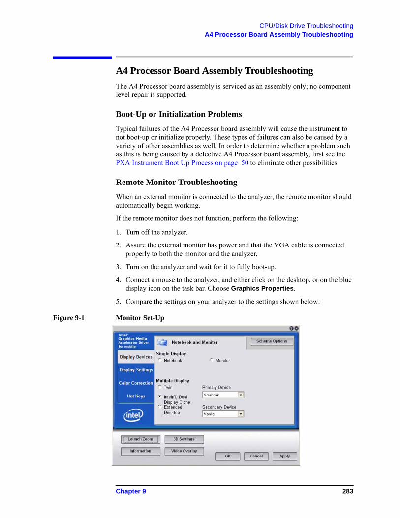
CPU/Disk Drive Troubleshooting
A4 Processor Board Assembly Troubleshooting
A4 Processor Board Assembly Troubleshooting
The A4 Processor board assembly is serviced as an assembly only; no component level repair is supported.
Boot-Up or Initialization Problems
Typical failures of the A4 Processor board assembly will cause the instrument to not boot-up or initialize properly. These types of failures can also be caused by a variety of other assemblies as well. In order to determine whether a problem such as this is being caused by a defective A4 Processor board assembly, first see the PXA Instrument Boot Up Process on page 50 to eliminate other possibilities.
Remote Monitor Troubleshooting
When an external monitor is connected to the analyzer, the remote monitor should automatically begin working.
If the remote monitor does not function, perform the following:
1. Turn off the analyzer.
2. Assure the external monitor has power and that the VGA cable is connected properly to both the monitor and the analyzer.
3. Turn on the analyzer and wait for it to fully boot-up.
4. Connect a mouse to the analyzer, and either click on the desktop, or on the blue display icon on the task bar. Choose Graphics Properties.
5. Compare the settings on your analyzer to the settings shown below:
Figure 9-1 Monitor Set-Up
Chapter 9 283
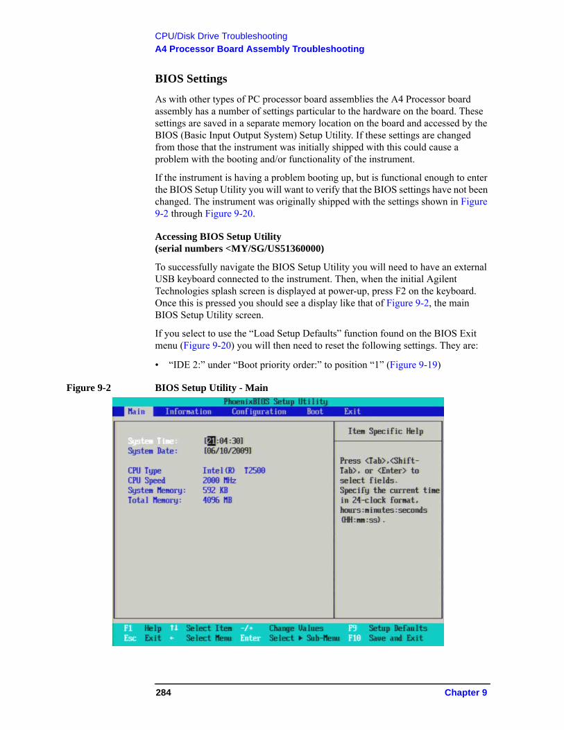
CPU/Disk Drive Troubleshooting
A4 Processor Board Assembly Troubleshooting
BIOS Settings
As with other types of PC processor board assemblies the A4 Processor board assembly has a number of settings particular to the hardware on the board. These settings are saved in a separate memory location on the board and accessed by the BIOS (Basic Input Output System) Setup Utility. If these settings are changed from those that the instrument was initially shipped with this could cause a problem with the booting and/or functionality of the instrument.
If the instrument is having a problem booting up, but is functional enough to enter the BIOS Setup Utility you will want to verify that the BIOS settings have not been changed. The instrument was originally shipped with the settings shown in Figure 9-2 through Figure 9-20.
Accessing BIOS Setup Utility(serial numbers <MY/SG/US51360000)
To successfully navigate the BIOS Setup Utility you will need to have an external USB keyboard connected to the instrument. Then, when the initial Agilent Technologies splash screen is displayed at power-up, press F2 on the keyboard. Once this is pressed you should see a display like that of Figure 9-2, the main BIOS Setup Utility screen.
If you select to use the “Load Setup Defaults” function found on the BIOS Exit menu (Figure 9-20) you will then need to reset the following settings. They are:
• “IDE 2:” under “Boot priority order:” to position “1” (Figure 9-19)
Figure 9-2 BIOS Setup Utility - Main
284 Chapter 9
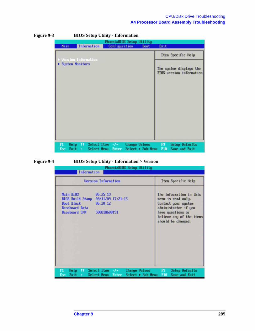
CPU/Disk Drive Troubleshooting
A4 Processor Board Assembly Troubleshooting
Figure 9-3 BIOS Setup Utility - Information
Figure 9-4 BIOS Setup Utility - Information > Version
Chapter 9 285
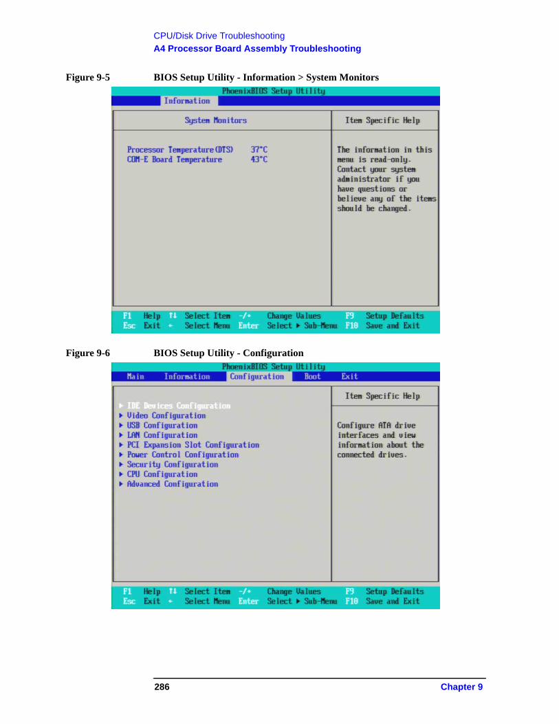
CPU/Disk Drive Troubleshooting
A4 Processor Board Assembly Troubleshooting
Figure 9-5 BIOS Setup Utility - Information > System Monitors
Figure 9-6 BIOS Setup Utility - Configuration
286 Chapter 9
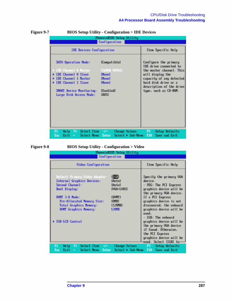
CPU/Disk Drive Troubleshooting
A4 Processor Board Assembly Troubleshooting
Figure 9-7 BIOS Setup Utility - Configuration > IDE Devices
Figure 9-8 BIOS Setup Utility - Configuration > Video
Chapter 9 287
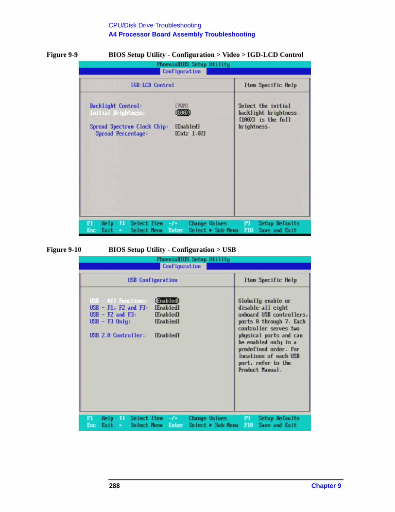
CPU/Disk Drive Troubleshooting
A4 Processor Board Assembly Troubleshooting
Figure 9-9 BIOS Setup Utility - Configuration > Video > IGD-LCD Control
Figure 9-10 BIOS Setup Utility - Configuration > USB
288 Chapter 9
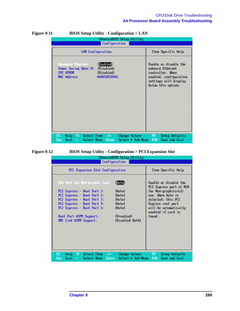
CPU/Disk Drive Troubleshooting
A4 Processor Board Assembly Troubleshooting
Figure 9-11 BIOS Setup Utility - Configuration > LAN
Figure 9-12 BIOS Setup Utility - Configuration > PCI Expansion Slot
Chapter 9 289
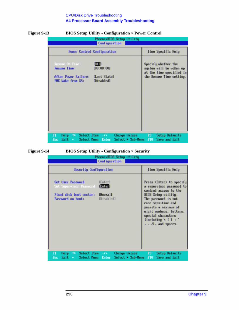
CPU/Disk Drive Troubleshooting
A4 Processor Board Assembly Troubleshooting
Figure 9-13 BIOS Setup Utility - Configuration > Power Control
Figure 9-14 BIOS Setup Utility - Configuration > Security
290 Chapter 9
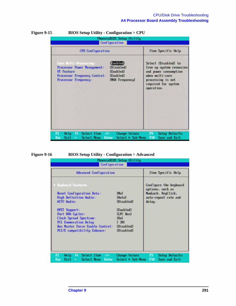
CPU/Disk Drive Troubleshooting
A4 Processor Board Assembly Troubleshooting
Figure 9-15 BIOS Setup Utility - Configuration > CPU
Figure 9-16 BIOS Setup Utility - Configuration > Advanced
Chapter 9 291
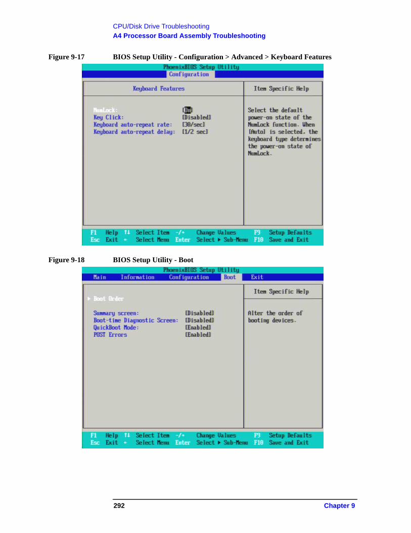
CPU/Disk Drive Troubleshooting
A4 Processor Board Assembly Troubleshooting
Figure 9-17 BIOS Setup Utility - Configuration > Advanced > Keyboard Features
Figure 9-18 BIOS Setup Utility - Boot
292 Chapter 9
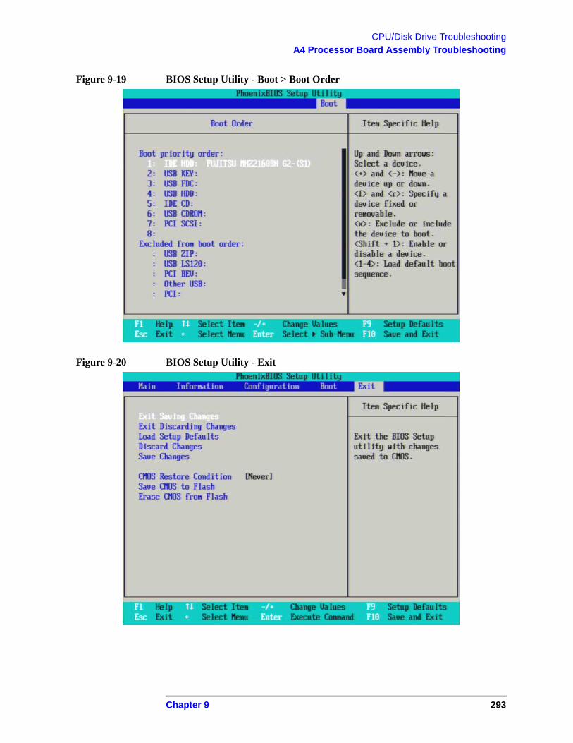
CPU/Disk Drive Troubleshooting
A4 Processor Board Assembly Troubleshooting
Figure 9-19 BIOS Setup Utility - Boot > Boot Order
Figure 9-20 BIOS Setup Utility - Exit
Chapter 9 293
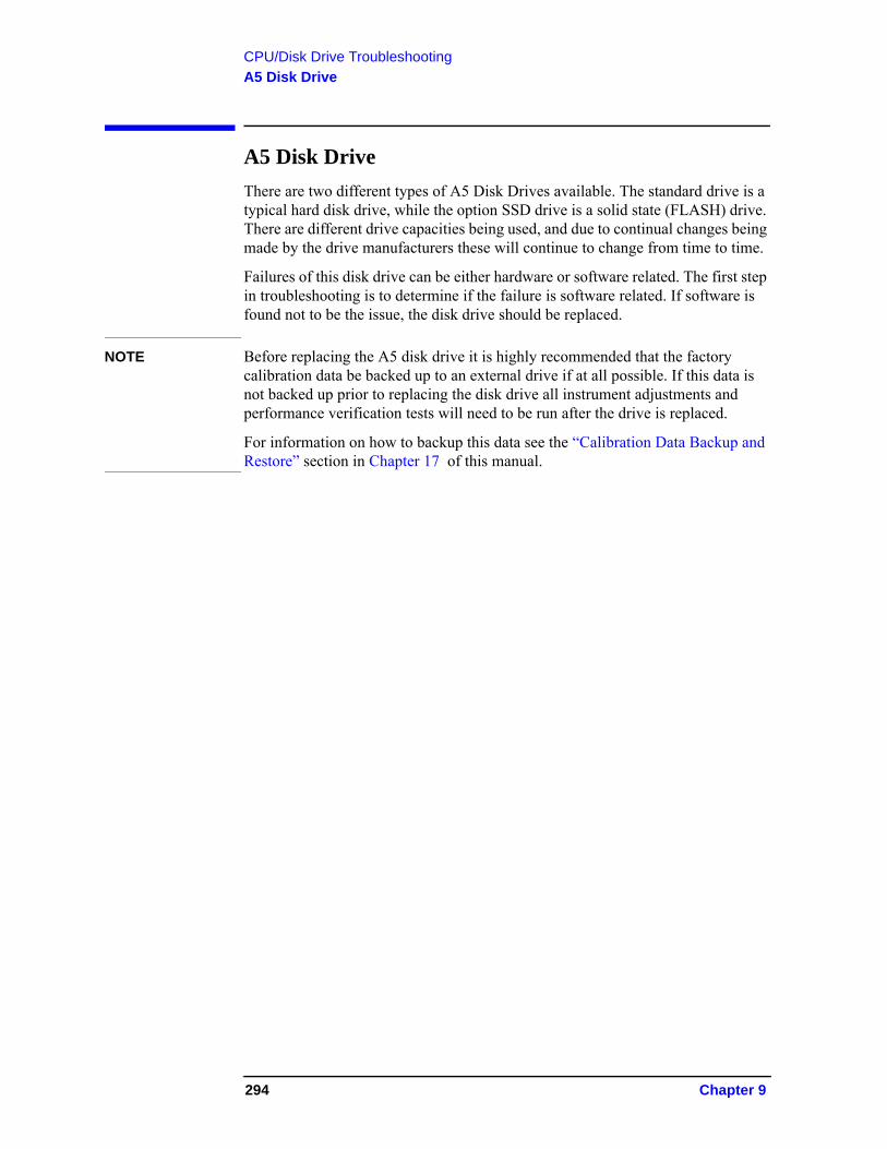
CPU/Disk Drive Troubleshooting
A5 Disk Drive
A5 Disk Drive
There are two different types of A5 Disk Drives available. The standard drive is a typical hard disk drive, while the option SSD drive is a solid state (FLASH) drive. There are different drive capacities being used, and due to continual changes being made by the drive manufacturers these will continue to change from time to time.
Failures of this disk drive can be either hardware or software related. The first step in troubleshooting is to determine if the failure is software related. If software is found not to be the issue, the disk drive should be replaced.
NOTE Before replacing the A5 disk drive it is highly recommended that the factory calibration data be backed up to an external drive if at all possible. If this data is not backed up prior to replacing the disk drive all instrument adjustments and performance verification tests will need to be run after the drive is replaced.
For information on how to backup this data see the “Calibration Data Backup and Restore” section in Chapter 17 of this manual.
294 Chapter 9
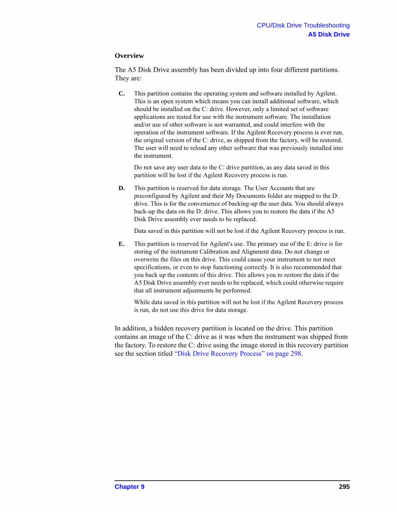
CPU/Disk Drive Troubleshooting
A5 Disk Drive
Overview
The A5 Disk Drive assembly has been divided up into four different partitions. They are:
In addition, a hidden recovery partition is located on the drive. This partition contains an image of the C: drive as it was when the instrument was shipped from the factory. To restore the C: drive using the image stored in this recovery partition see the section titled “Disk Drive Recovery Process” on page 298.
C. This partition contains the operating system and software installed by Agilent. This is an open system which means you can install additional software, which should be installed on the C: drive. However, only a limited set of software applications are tested for use with the instrument software. The installation and/or use of other software is not warranted, and could interfere with the operation of the instrument software. If the Agilent Recovery process is ever run, the original version of the C: drive, as shipped from the factory, will be restored. The user will need to reload any other software that was previously installed into the instrument.
Do not save any user data to the C: drive partition, as any data saved in this partition will be lost if the Agilent Recovery process is run.
D. This partition is reserved for data storage. The User Accounts that are preconfigured by Agilent and their My Documents folder are mapped to the D: drive. This is for the convenience of backing-up the user data. You should always back-up the data on the D: drive. This allows you to restore the data if the A5 Disk Drive assembly ever needs to be replaced.
Data saved in this partition will not be lost if the Agilent Recovery process is run.
E. This partition is reserved for Agilent's use. The primary use of the E: drive is for storing of the instrument Calibration and Alignment data. Do not change or overwrite the files on this drive. This could cause your instrument to not meet specifications, or even to stop functioning correctly. It is also recommended that you back up the contents of this drive. This allows you to restore the data if the A5 Disk Drive assembly ever needs to be replaced, which could otherwise require that all instrument adjustments be performed.
While data saved in this partition will not be lost if the Agilent Recovery process is run, do not use this drive for data storage.
Chapter 9 295
CPU/Disk Drive Troubleshooting
Troubleshooting software related issues
Troubleshooting software related issues
The C: drive contains the Windows XP operating system software and the X-Series software. Boot problems can be caused by either a failure of the Windows XP operating system or the X-Series software. The failure could have occurred due to a failed installation procedure, X-Series software update failure or a virus.
To correct these issues there are two procedures that can be initiated to resolve a software related issue.
• Reload the X-Series software.
• Use the Recovery Process to reinstall the Windows XP operating system and X-Series software as it was when it left the factory.
296 Chapter 9
CPU/Disk Drive Troubleshooting
Reloading the X-Series Software
Reloading the X-Series Software
The X-Series software contains all the required components for the signal analyzer application as well as all software options. If the X-Series software has become corrupt the Windows XP operating system will boot but the X-Series software application will fail to start. In these cases go to Chapter 19 , “Instrument Software,” for information on how to update the X-Series software. This procedure will not affect the instrument’s calibration or user files.
If this does not resolve the boot issue, or the instrument never boots the Windows XP operating system proceed to the “Disk Drive Recovery Process”.
Chapter 9 297
CPU/Disk Drive Troubleshooting
Disk Drive Recovery Process
Disk Drive Recovery Process
The Agilent Recovery System can be used to repair errors on the instrument's C: drive partition or to restore the original factory configuration of the system software. The Agilent Recovery System is stored in a separate hidden hard disk drive partition.
Repairing errors on the hard disk drive may result in loss of data or files. If you need more information about the Windows “chkdsk” error repair process, see the chkdsk documentation in the Microsoft Windows XP Help and Support Center.
Restoring the original factory system software does not restore any of the following items:
• Windows system configurations that were made after the instrument was shipped from the factory. For example, Windows and Service Pack updates, user accounts, and windows configuration settings. After an Agilent Recovery, these configurations need to be redone.
• Additional software that was installed after the instrument was shipped from the factory. After an Agilent Recovery, that software needs to be re-installed.
• Any data or programs saved on the D: or E: drives.
• Any upgrades that were made to the Agilent measurement application software.
Restoring the original factory system software will not synchronize the code in the Field Programmable Gate Arrays (FPGAs) on the various hardware assemblies. As a result, you may see an error dialog box appear during the final boot-up at the end of the recovery process. This typically occurs when there are significant differences between the software version installed prior to performing the recovery and the version restored by the recovery. In these situations, upgrade the software to the latest version.
Calibration data is not lost during this process because it resides on the E drive partition.
298 Chapter 9
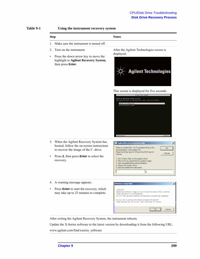
CPU/Disk Drive Troubleshooting
Disk Drive Recovery Process
Table 9-1 Using the instrument recovery system
Step Notes
1. Make sure the instrument is turned off.
2. Turn on the instrument.
• Press the down arrow key to move the highlight to Agilent Recovery System, then press Enter.
After the Agilent Technologies screen is displayed,
This screen is displayed for five seconds.
3. When the Agilent Recovery System has booted, follow the on-screen instructions to recover the image of the C: drive.
• Press 2, then press Enter to select the recovery.
4. A warning message appears.
• Press Enter to start the recovery, which may take up to 25 minutes to complete.
After exiting the Agilent Recovery System, the instrument reboots.
Update the X-Series software to the latest version by downloading it from the following URL:
www.agilent.com/find/xseries_software
Chapter 9 299

CPU/Disk Drive Troubleshooting
Disk Drive Recovery Process
Replacing the instrument disk drive
If the above two procedures did not resolve the booting issue. The disk drive should be replaced. Please refer to the “Disk Drive” replacement section on page 510.
300 Chapter 9

10 Power Supply/Midplane Troubleshooting
301
Power Supply/Midplane Troubleshooting
What You Will Find in This Chapter
What You Will Find in This Chapter
The following information is presented in this chapter:
1. Theory of operation of the Power Supply/Midplane section.2. Isolating the cause of a hardware problem by verifying the functionality of
assemblies in the Power Supply and Midplane sections.
NOTE Each of the following sections first describes how the assembly works, then gives information to help you troubleshoot the assembly. Each description explains the purpose of the assembly, describes the main components, and lists external connections to the assembly.
This following descriptions are found in this chapter:
A6 Power Supply Description on page 303
A6 Power Supply Assembly Troubleshooting on page 307
A7 Midplane Board Assembly Description on page 310
A7 Midplane Board Assembly Troubleshooting on page 312
302 Chapter 10
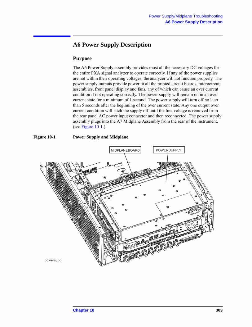
Power Supply/Midplane Troubleshooting
A6 Power Supply Description
A6 Power Supply Description
Purpose
The A6 Power Supply assembly provides most all the necessary DC voltages for the entire PXA signal analyzer to operate correctly. If any of the power supplies are not within their operating voltages, the analyzer will not function properly. The power supply outputs provide power to all the printed circuit boards, microcircuit assemblies, front panel display and fans, any of which can cause an over current condition if not operating correctly. The power supply will remain on in an over current state for a minimum of 1 second. The power supply will turn off no later than 5 seconds after the beginning of the over current state. Any one output over current condition will latch the supply off until the line voltage is removed from the rear panel AC power input connector and then reconnected. The power supply assembly plugs into the A7 Midplane Assembly from the rear of the instrument. (see Figure 10-1.)
Figure 10-1 Power Supply and Midplane
Chapter 10 303
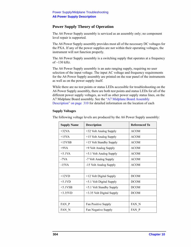
Power Supply/Midplane Troubleshooting
A6 Power Supply Description
Power Supply Theory of Operation
The A6 Power Supply assembly is serviced as an assembly only; no component level repair is supported.
The A6 Power Supply assembly provides most all of the necessary DC voltages for the PXA. If any of the power supplies are not within their operating voltages, the instrument will not function properly.
The A6 Power Supply assembly is a switching supply that operates at a frequency of ~130 kHz.
The A6 Power Supply assembly is an auto ranging supply, requiring no user selection of the input voltage. The input AC voltage and frequency requirements for the A6 Power Supply assembly are printed on the rear panel of the instruments as well as on the power supply itself.
While there are no test points or status LEDs accessible for troubleshooting on the A6 Power Supply assembly, there are both test points and status LEDs for all of the different power supply voltages, as well as other power supply status lines, on the A7 Midplane Board assembly. See the “A7 Midplane Board Assembly Description” on page 310 for detailed information on the location of each
Supply Voltages
The following voltage levels are produced by the A6 Power Supply assembly:
Supply Name Description Referenced To
+32VA +32 Volt Analog Supply ACOM
+15VA +15 Volt Analog Supply ACOM
+15VSB +15 Volt Standby Supply ACOM
+9VA +9 Volt Analog Supply ACOM
+5.1VA +5.1 Volt Analog Supply ACOM
-7VA -7 Volt Analog Supply ACOM
-15VA -15 Volt Analog Supply ACOM
+12VD +12 Volt Digital Supply DCOM
+5.1VD +5.1 Volt Digital Supply DCOM
+5.1VSB +5.1 Volt Standby Supply DCOM
+3.35VD +3.35 Volt Digital Supply DCOM
FAN_P Fan Positive Supply FAN_N
FAN_N Fan Negative Supply FAN_P
304 Chapter 10
Power Supply/Midplane Troubleshooting
A6 Power Supply Description
Control Inputs
There are a number of control inputs for the A6 Power Supply assembly. The ones that you will want to be familiar with are:
POWER_ON_L is a signal that when pulled low tells the A6 Power Supply assembly to turn on all of its outputs. This signal comes from the A4 CPU board assembly and is initiated by pressing the front panel power button.
DITHER is an AC coupled analog signal going to the supply that is used to frequency modulate the power supply switching frequency for the purpose of lowering any power supply related interference. The DITHER signal is generated on the A7 Midplane board assembly.
Control/Status Outputs
There are a number of control and status outputs for the A6 Power Supply assembly. The ones that you will want to be familiar with are:
POWER_OK is used to verify that the +12VD, +5.1VD, and +3.35VD are all on and within specification. A TTL high level on this output brings the CPU out of reset and initiates the instrument boot up process.
LINE_TRIGGER is a TTL level signal that is synchronous to the AC line input. This signal is typically used in spectrum analyzers to trigger an instrument sweep synchronous to the AC power line.
FAULT_L will be a TTL low level signal to indicate that the supply is experiencing an over voltage, over current, or over temperature condition.
Fuse
The A6 Power Supply has no user replaceable fuse. While there is a fuse internal to the supply this is not meant for field replacement. If the internal fuse is blown, the power supply has experienced a major failure and should be replaced.
Standby Supplies
The A6 Power Supply assembly has two standby supplies that should always be on if the AC input voltage requirements are met. These are the +15VSB and the +5.1VSB supplies. These supplies are used by the instrument to keep certain circuits alive even when the power is turned off.
Over Current Protection
The A6 Power Supply assembly has built in over current protection that will shut down the supply if current draw from the instrument is too great. The power supply will remain on in over current state for a minimum of 1 second. The power supply shall turn off no later than 5 seconds after the beginning of the over current state. The power supply shall remain off until the line voltage is removed and then
Chapter 10 305
Power Supply/Midplane Troubleshooting
A6 Power Supply Description
reconnected or the front panel power switch is cycled. Over current shut down does not apply to the standby supplies, the fan voltage, and the +32VA supply.
Thermal Protection
The A6 Power Supply assembly will protect itself by shutting down if it overheats. It will also reset itself with no user interaction after the temperature is reduced by approximately 10 degrees C.
306 Chapter 10
Power Supply/Midplane Troubleshooting
A6 Power Supply Assembly Troubleshooting
A6 Power Supply Assembly Troubleshooting
The A6 Power Supply assembly is serviced as an assembly only; no component level repair is supported.
NOTE The A6 Power Supply has no user replaceable fuse. While there is a fuse internal to the supply this is not meant for field replacement. If the internal fuse is blown, the power supply has experienced a major failure and should be replaced.
If the instrument will not boot up properly, or the display is not turning on, refer to the PXA Instrument Boot Up Process on page 50 before further A6 Power Supply troubleshooting to rule out any other assembly as the cause of the failure.
Supply Voltages
While there are no test points or status LEDs accessible for troubleshooting on the A6 Power Supply assembly, there are both test points and status LEDs for all of the different power supply voltages, as well as other power supply status lines, on the A7 Midplane Board assembly. See the A7 Midplane Board Assembly section in this chapter for detailed information on the location of each.
Chapter 10 307
Power Supply/Midplane Troubleshooting
A6 Power Supply Assembly Troubleshooting
Control Inputs
POWER_ON
POWER_ON is a signal that when pulled low tells the A6 Power Supply assembly to turn on all of its outputs. This signal comes from the A4 Processor board assembly and is initiated by pressing the front panel power button.
If the instrument will not turn on be sure that this line is being pulled low by either measuring the voltage level at Test Point 518 on the A7 Midplane board assembly or by viewing the status of the POWER_ON_L LED. See the "A7 Midplane Board Assembly Troubleshooting" on page 312 for detailed information on the location of this test point and LED as well as the expected status for both when the instrument is operating properly.
Status Outputs
POWER_OK
The POWER_OK status output is an indication of whether or not all of the digital power supply voltages are up to their specified voltage levels or not. If all of these supplies are working properly this output line will be at a TTL high level. If this output is not at a TTL High level the instrument CPU will not come out of its reset state and will not boot-up. Once this output goes to a TTL high level the instrument CPU will start its boot-up process and the POWER_ON_L line coming from the A4 Processor assembly will go to a TTL low level which will tell the A6 Power Supply assembly to turn on the rest of it output voltages.
If the A6 Power Supply assembly is suspected of causing the instrument to not power on properly the status of this output can be verified by either measuring the voltage level at Test Point 506 on the A7 Midplane board assembly or by viewing the status of the POWER_OK LED. See the A7 Midplane Board Assembly Troubleshooting section in this chapter for detailed information on the location of this test point and LED as well as the expected status for both when the instrument is operating properly.
FAULT_L
The FAULT_L status output is an indication of whether or not there is a fault detected by the A6 Power Supply that is keeping it from powering on properly. If all of the required conditions to turn the A6 Power Supply assembly on properly are being met this status output line will be at a TTL high level. The conditions that could cause this status output line to be at a TTL low level include that of an over current condition, an over voltage condition, and an over temperature condition. However, there is no way to know at the A6 Power Supply assembly level which one of these conditions may be the cause of a TTL low level to be on the FAULT_L status output.
While any over voltage or over temperature conditions will most likely be caused by an A6 Power Supply assembly failure, an over current condition
308 Chapter 10

Power Supply/Midplane Troubleshooting
A6 Power Supply Assembly Troubleshooting
will most likely be caused by another assembly in the instrument demanding too much current.
If this output is not at a TTL high level the A6 Power Supply assembly will not turn its non-standby power supplies on, no matter what the A4 Processor assembly tells it to do.
If the A6 Power Supply assembly is suspected of causing the instrument to not power on properly the status of this output line can be verified by either measuring the voltage level at Test Point 508 on the A7 Midplane board assembly or by viewing the status of the FAULT_L LED. See the A7 Midplane Board AssemblyTroubleshooting section in this chapter for detailed information on the location of this test point and LED as well as the expected status for both when the instrument is operating properly.
Chapter 10 309
Power Supply/Midplane Troubleshooting
A7 Midplane Board Assembly Description
A7 Midplane Board Assembly Description
The A7 Midplane board assembly is used to connect the A4 Processor board assembly and the A6 Power Supply assembly to the A8 Motherboard, and thus the rest of the instrument electrical assemblies.
In addition, the A7 Midplane board also provides the following functions:
• Instrument power supply voltage test points and status LEDs
• +3.3V analog linear power supply regulation (+3.3VA)
• -5.2V analog linear power supply regulation (-5.2VA)
• Non-volatile memory for storage of the instrument model number, serial number, and software license keys (Secure Storage).
• Power supply dithering. A triangle wave of approximately 100 Hz is generated and goes directly to the A6 Power Supply assembly. This is used to frequency modulate the power supply switching frequency for the purpose of lowering any power supply related interference.
• Circuitry to phase lock the A4 Processor assembly CPU clock to the instrument reference frequency.
Midplane Board Connections
Connector Connects To Connector Connects To
J101 A6 Power Supply Assembly J111 A6 Power Supply Assembly
J102 A6 Power Supply Assembly J112 A6 Power Supply Assembly
J103 A6 Power Supply Assembly J201 A4 Processor Assembly
J104 A6 Power Supply Assembly J202 A4 Processor Assembly
J105 A6 Power Supply Assembly J203 A4 Processor Assembly
J106 A6 Power Supply Assembly J204 A4 Processor Assembly
J107 A6 Power Supply Assembly P1 A8 Motherboard Assembly
J108 A6 Power Supply Assembly P2 A8 Motherboard Assembly
J109 A6 Power Supply Assembly P3 A8 Motherboard Assembly
J110 A6 Power Supply Assembly P13 A8 Motherboard Assembly
310 Chapter 10
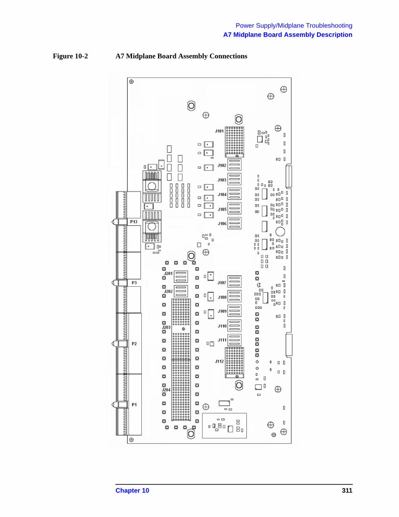
Power Supply/Midplane Troubleshooting
A7 Midplane Board Assembly Description
Figure 10-2 A7 Midplane Board Assembly Connections
Chapter 10 311
Power Supply/Midplane Troubleshooting
A7 Midplane Board Assembly Troubleshooting
A7 Midplane Board Assembly Troubleshooting
The A7 Midplane board assembly is serviced as an assembly only; no component level repair is supported.
Instrument Power Supply LEDs and Test Points
While the A6 Power Supply assembly has no user accessible LEDs or test points the A7 Midplane board assembly does provide these for all of the different instrument power supplies as well as many of the power supply status lines. A complete list of these can be found in Table 10-1 and the location of each can be seen in Figure 10-3.
Additional Power Supply Regulation
There are two analog power supply regulators on the A7 Midplane board assembly. They are the +3.3VA and -5.2VA supplies.
The +3.3VA supply is regulated down from the instrument +5.1VA supply while the -5.2VA supply is regulated down from the -7VA instrument supply.
Both of these supply voltages have test points and LEDs on the A7 Midplane board assembly as seen in Figure 10-3.
Instrument Secure Storage
This is Non-volatile storage of instrument model number, serial number, and software license keys. While the license keys are also contained on the C: drive of the instrument, the model and serial numbers are only saved in this secure memory. There is no way for the user to access this memory in any way. This is reserved for the factory and field software when needed for instrument initialization, as well as the instrument software when installing an option license key. If for some reason any of these cannot be remembered by the instrument there could be a problem with this memory and the A7 Midplane board assembly would need to be replaced.
Power Supply Dithering
A triangle wave of approximately 100 Hz is generated and goes directly to the A6 Power Supply assembly. This is used to frequency modulate the power supply switching frequency for the purpose of lowering any power supply related interference.
If for some reason the level of the power supply related interference is higher than normal this circuitry, or the A6 Power Supply assembly, could be suspect.
312 Chapter 10
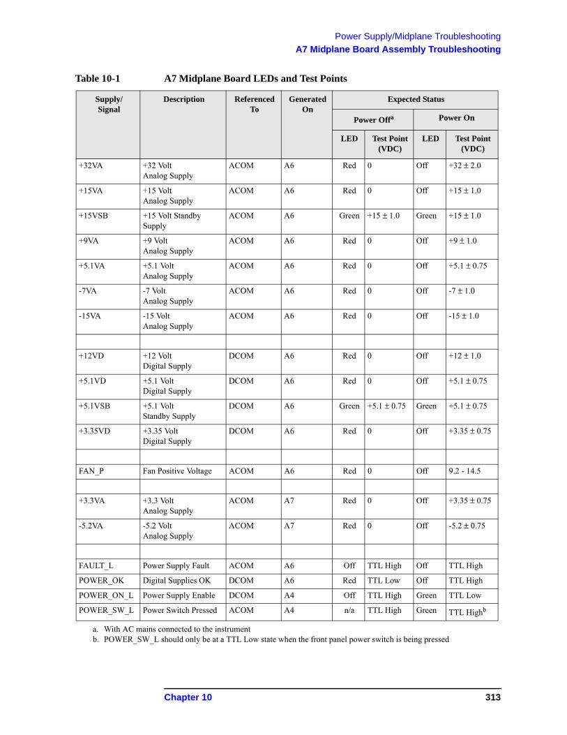
Power Supply/Midplane Troubleshooting
A7 Midplane Board Assembly Troubleshooting
Table 10-1 A7 Midplane Board LEDs and Test Points
Supply/Signal
Description ReferencedTo
Generated On
Expected Status
Power Offa Power On
LED Test Point(VDC)
LED Test Point(VDC)
+32VA +32 Volt Analog Supply
ACOM A6 Red 0 Off +32 ± 2.0
+15VA +15 Volt Analog Supply
ACOM A6 Red 0 Off +15 ± 1.0
+15VSB +15 Volt Standby Supply
ACOM A6 Green +15 ± 1.0 Green +15 ± 1.0
+9VA +9 Volt Analog Supply
ACOM A6 Red 0 Off +9 ± 1.0
+5.1VA +5.1 Volt Analog Supply
ACOM A6 Red 0 Off +5.1 ± 0.75
-7VA -7 Volt Analog Supply
ACOM A6 Red 0 Off -7 ± 1.0
-15VA -15 Volt Analog Supply
ACOM A6 Red 0 Off -15 ± 1.0
+12VD +12 Volt Digital Supply
DCOM A6 Red 0 Off +12 ± 1.0
+5.1VD +5.1 Volt Digital Supply
DCOM A6 Red 0 Off +5.1 ± 0.75
+5.1VSB +5.1 Volt Standby Supply
DCOM A6 Green +5.1 ± 0.75 Green +5.1 ± 0.75
+3.35VD +3.35 Volt Digital Supply
DCOM A6 Red 0 Off +3.35 ± 0.75
FAN_P Fan Positive Voltage ACOM A6 Red 0 Off 9.2 - 14.5
+3.3VA +3.3 Volt Analog Supply
ACOM A7 Red 0 Off +3.35 ± 0.75
-5.2VA -5.2 Volt Analog Supply
ACOM A7 Red 0 Off -5.2 ± 0.75
FAULT_L Power Supply Fault ACOM A6 Off TTL High Off TTL High
POWER_OK Digital Supplies OK DCOM A6 Red TTL Low Off TTL High
POWER_ON_L Power Supply Enable DCOM A4 Off TTL High Green TTL Low
POWER_SW_L Power Switch Pressed ACOM A4 n/a TTL High Green TTL Highb
a. With AC mains connected to the instrumentb. POWER_SW_L should only be at a TTL Low state when the front panel power switch is being pressed
Chapter 10 313
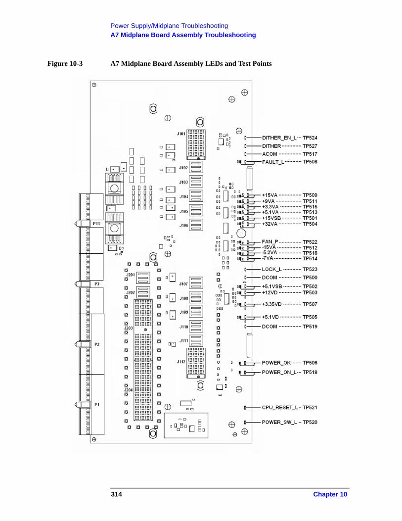
Power Supply/Midplane Troubleshooting
A7 Midplane Board Assembly Troubleshooting
Figure 10-3 A7 Midplane Board Assembly LEDs and Test Points
314 Chapter 10

11 Front Panel/Motherboard Troubleshooting
315
Front Panel/Motherboard Troubleshooting
What You Will Find in This Chapter
What You Will Find in This Chapter
The following information is found in this chapter:
1. Theory of operation of the Motherboard Assembly.2. Theory of operation of the Front Panel Assembly.3. Isolating the cause of an hardware problem by verifying the functionality of
assemblies.
This following descriptions are found in this chapter:
• A8 Motherboard Description ............................................................... page 317• A1 Front Panel Assembly .................................................................... page 320
316 Chapter 11
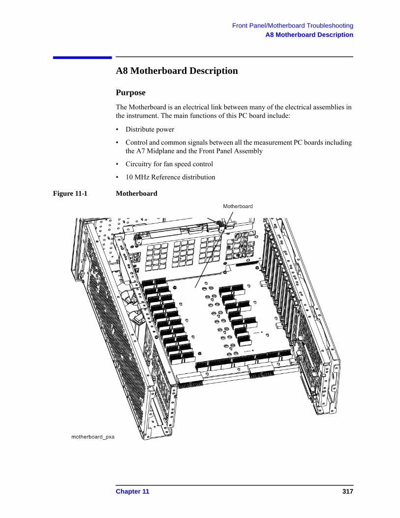
Front Panel/Motherboard Troubleshooting
A8 Motherboard Description
A8 Motherboard Description
Purpose
The Motherboard is an electrical link between many of the electrical assemblies in the instrument. The main functions of this PC board include:
• Distribute power
• Control and common signals between all the measurement PC boards including the A7 Midplane and the Front Panel Assembly
• Circuitry for fan speed control
• 10 MHz Reference distribution
Figure 11-1 Motherboard
Chapter 11 317
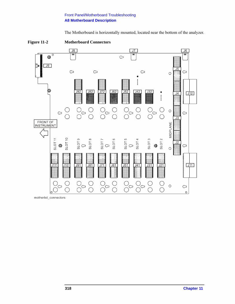
Front Panel/Motherboard Troubleshooting
A8 Motherboard Description
The Motherboard is horizontally mounted, located near the bottom of the analyzer.
Figure 11-2 Motherboard Connectors
318 Chapter 11
Front Panel/Motherboard Troubleshooting
A8 Motherboard Description
A8 Motherboard Troubleshooting
There are no troubleshooting procedures for this assembly. If the Motherboard is suspect, it must be replaced.
MotherboardConnector
What Plugs In? MotherboardConnector
What Plugs In?
J2 A7, Midplane J11 A3, Digital I.F, analog signals
J3 A7, Midplane J12 A3, Digital I.F, analog signals
J4 A7, Midplane J21 A16, Reference
J5 A7, Midplane J31/J32 Option Slots
J6 B3, Fan J41/J42 Option Slots
J7 B2, Fan J51/J52 Option Slots
J8 B1, Fan J61/J62 Option Slots
J9 Front Panel J71/J72 Option Slots
J81/J82 Option Slots
J91/J92 Option Slots
J101 A14, LO Synthesizer
J111 A15, Front End Control
Chapter 11 319
Front Panel/Motherboard Troubleshooting
A1 Front Panel Assembly
A1 Front Panel Assembly
The major components of the A1 Front Frame Assembly are the A1A2 Front Panel Interface Board, A1A3 LCD, A1A4 LCD Inverter Board/DC-DC Converter, and the A1A5 Front Panel USB Interface Board, all of which are serviceable as individual components.
The A1 assembly is used to display the measurement results, accept user input via the keyboard, and connect USB peripheral devices.
A1A2 Front Panel Interface Board
The A1A2 Front Panel Interface board is serviced as an assembly only; no component level repair is supported.
The Front Panel Interface Board contains LCD control, Inverter drive, audio amplifiers, internal speaker, a 4 port USB hub, and a USB keyboard microcontroller.
The two different front panel rubber keypads attach to the back side of the board, which has the keyboard contacts printed on the reverse side.
The 4 ports from the USB hub contained on this board go to the 2 front panel USB connectors, the keyboard microcontroller, and the fourth port is unused.
A1A3 LCD
The LCD used is an 8.4inch XGA TFT display, which has a resolution of 1024 x 768. It has two backlights that are not individually replaceable.
A1A4 LCD Inverter Board/DC-DC Converter
The Inverter Board provides the high voltage required by the LCD backlights used on older PXA’s. Newer PXA’s use a DC-DC converter to power the LED backlights.
A1A5 Front Panel USB Interface Board
The Front Panel USB Interface Board provides the front panel USB connections.
320 Chapter 11
12 Hardware Options
321
Hardware Options
What You Will Find in This Chapter
What You Will Find in This Chapter
The following information is found in this chapter.
A25 Wideband Analog IF and A26 Digital IF Troubleshooting on page 325
Option BBA Analog I/Q Baseband Inputs Description on page 331
The PXA signal analyzer has a variety of hardware options that can be purchased and installed at the time of new instrument sale, or as a post-sale upgrade. Some of these hardware options require the installation of additional hardware, and others require licensing hardware already present in the standard instrument hardware configuration.
A current list of all instrument options and retrofit requirements is available on the Agilent web site for the PXA signal analyzer at:
http://www.agilent.com/find/PXA_upgrades
Table 12-1 Hardware Options
Option Description Additional Hardware or License Only
Service Guide Section
ALV Auxiliary Log Video (at rear panel Aux IF connector)
License Only Chapter 6 , “Front End Control Troubleshooting”
B25 25 MHz Information Bandwidth path License Only Chapter 7 , “Analog/Digital IF Troubleshooting”
B40 40 MHz Information Bandwidth path in addition to 25 MHz BW
License Only Chapter 7 , “Analog/Digital IF Troubleshooting”
B1X 140 MHz Information Bandwidth path in addition to the 25 MHZ and 40 MHz BW
Additional hardware This chapter
B1Y Analysis Bandwidth Extension, 160 MHz
License Only
BBA Analog I/Q Baseband Inputs Additional Hardware This chapter
CRP Arbitrary IF Output (10 MHz to 75 MHz programmable, Aux IF connector on rear panel).
License Only Chapter 6 , “Front End Control Troubleshooting”
CR3 2nd IF Out (Aux IF connector on rear panel)
License Only Chapter 6 , “Front End Control Troubleshooting”
322 Chapter 12
Hardware Options
What You Will Find in This Chapter
EA3 Electronic Attenuator License Only Chapter 4 , “RF Section Troubleshooting (RF/Microwave Analyzers)”
EXM External Mixing Additional Hardware Chapter 4 , “RF Section Troubleshooting (RF/Microwave Analyzers)” and Chapter 5 , “RF Section Troubleshooting (Millimeter-Wave Analyzers)”
LNP Low Noise Path(Bypasses A11 Low Band Switch, used in high band only)
Additional hardware or license only depending on current instrument configuration. Both LNP and MPB hardware installed at same time. However, there may be cases where only one option is licensed.
Chapter 4 , “RF Section Troubleshooting (RF/Microwave Analyzers)”
Chapter 16, “Options MPB and LNP” on page 449
MPB Preselector Bypass(Bypasses the A12 Preselector filter used above 3.6 GHz)
Additional hardware or license only depending on current instrument configuration. Both LNP and MPB hardware installed at same time. However, there may be cases where only one option is licensed
Chapter 4 , “RF Section Troubleshooting (RF/Microwave Analyzers)”
Chapter 16, “Options MPB and LNP” on page 449
P03 Preamp, 100 kHz to 3.6 GHz License Only Chapter 4 , “RF Section Troubleshooting (RF/Microwave Analyzers)”
P08 Preamp, 100 kHz to 8.4 GHz License Only Chapter 4 , “RF Section Troubleshooting (RF/Microwave Analyzers)”
Table 12-1 Hardware Options
Option Description Additional Hardware or License Only
Service Guide Section
Chapter 12 323
Hardware Options
What You Will Find in This Chapter
NOTE See Chapter 13 , “Block Diagrams” for information on how these hardware options are installed in the signal path.
P13 Preamp, 100 kHz to 13.6 GHz License Only Chapter 4 , “RF Section Troubleshooting (RF/Microwave Analyzers)”
P26 Preamp, 100 kHz to 26.5 GHz License Only Chapter 4 , “RF Section Troubleshooting (RF/Microwave Analyzers)”
P43 Preamp, 100 kHz to 43 GHz License Only Chapter 5 , “RF Section Troubleshooting (Millimeter-Wave Analyzers)”
P44 Preamp, 100 kHz to 44 GHz License Only Chapter 5 , “RF Section Troubleshooting (Millimeter-Wave Analyzers)”
P50 Preamp, 100 kHz to 50 GHz License Only Chapter 5 , “RF Section Troubleshooting (Millimeter-Wave Analyzers)”
RTL Data Link that enables rear panel Digital Bus connector.
License Only
YAV Screen Video (at rear panel Analog Out connector)
License Only Chapter 7 , “Analog/Digital IF Troubleshooting”
Table 12-1 Hardware Options
Option Description Additional Hardware or License Only
Service Guide Section
324 Chapter 12
Hardware Options
A25 Wideband Analog IF and A26 Digital IF Troubleshooting
A25 Wideband Analog IF and A26 Digital IF Troubleshooting
A25 Wideband Analog IF Assembly Description
The analyzer's RF input signal is down converted to a 300 MHz intermediate frequency by the A13 Front End assembly and routed through the A15 Front End controller to A15J901. Cable W41 connects A15J901 to the input of the A25 Wideband Analog IF at J101. The signal is filtered, attenuation and gain applied based upon the instrument settings. This signal is then sampled by the ADC and the resultant data is the sent to the A26 Wideband Digital IF for processing via the J2 ribbon cable. The A26 Wideband Digital IF has no service accessible locations and should be troubleshot from the front panel controls.
Chapter 12 325
326
Ch
apter 12
Hardw
are Options
A2
5 Wid
eba
nd
An
alog
IF an
d A
26
Dig
ital IF T
rou
ble
sho
otin
g
Figure 12-1 Analog IF Block Diagram
Hardware Options
A25 Wideband Analog IF and A26 Digital IF Troubleshooting
Inputs to the A25 Assembly
A25J101 300 MHz IF signal (from A15J901 Front End Controller)
A25J301 2400 MHz reference from A16 Reference Assembly via W34 cable
A25J805 Step Calibrator from A3J17 40 MHz Digital IF via W45 cable
Outputs from the A25 Assembly
A25J302 2400 MHz Reference Out
A25J102 300 MHz IF Out to A3J16 of the 40 MHz Digital IF
A25J806 50 MHz Comb Out to A16 Reference assembly A16J726 via W46 cable
A25J2 ADC Data to 140 MHz Digital IF A26J504 via W2 cable
A25 Wideband Analog IF Assembly Theory of Operation
The A25 Wideband Analog IF assembly primary role is to properly filter and apply attenuation or gain to optimize the level going to the ADC and provide sufficient pre-filtering to reject images that would otherwise interfere with the signal of interest. Precision alignments are used to calibrate the filters, attenuators and gain of this assembly. It is not uncommon that the reported failure will come from failures reported when an alignment fails for this assembly. The alignment history file is a good indicator of a failure for this assembly. This file is a text file that can be edited with Notepad. The file is located in the following location:
E:\AlignDataStore\AlignmentHistory.txt
This file will list all alignments that have passed or failed. Alignments reporting a failure of the WBAIF assembly can in many cases be attributed to failure of this assembly. If however these errors follow errors in the RF section of the instrument, it is possible that additional WBAIF error will appear due to missing RF Calibration signals and not related to the A25 Wideband IF assembly.
Manually troubleshoot the assembly is basically verifying the 300 MHz IF signal is present and at the proper level. In addition you will want to verify input and output levels of the various calibration and reference signals.
Additionally, the A25 Analog IF has a built in RF Burst Trigger that is available when the 140 MHz IF path is selected
Chapter 12 327
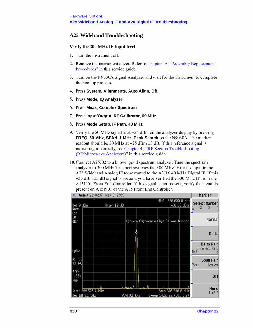
Hardware Options
A25 Wideband Analog IF and A26 Digital IF Troubleshooting
A25 Wideband Troubleshooting
Verify the 300 MHz IF Input level
1. Turn the instrument off.
2. Remove the instrument cover. Refer to Chapter 16, “Assembly Replacement Procedures” in this service guide.
3. Turn on the N9030A Signal Analyzer and wait for the instrument to complete the boot up process.
4. Press System, Alignments, Auto Align, Off.
5. Press Mode, IQ Analyzer
6. Press Meas, Complex Spectrum
7. Press Input/Output, RF Calibrator, 50 MHz
8. Press Mode Setup, IF Path, 40 MHz
9. Verify the 50 MHz signal is at −25 dBm on the analyzer display by pressing FREQ, 50 MHz, SPAN, 1 MHz, Peak Search on the N9030A. The marker readout should be 50 MHz at −25 dBm ±3 dB. If this reference signal is measuring incorrectly, see Chapter 4 , “RF Section Troubleshooting (RF/Microwave Analyzers)” in this service guide.
10.Connect A25J02 to a known good spectrum analyzer. Tune the spectrum analyzer to 300 MHz.This port switches the 300 MHz IF that is input to the A25 Wideband Analog IF to be routed to the A3J16 40 MHz Digital IF. If this −30 dBm ±3 dB signal is present, you have verified the 300 MHz IF from the A15J901 Front End Controller. If this signal is not present, verify the signal is present on A15J901 of the A15 Front End Controller.
328 Chapter 12
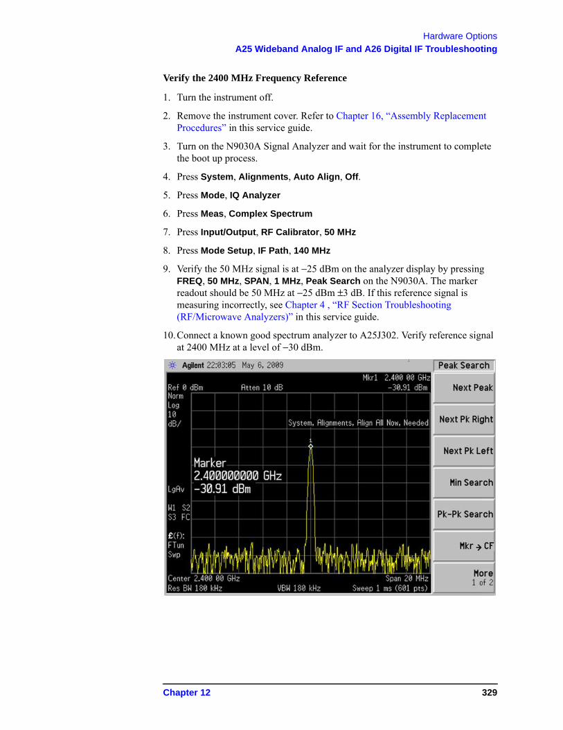
Hardware Options
A25 Wideband Analog IF and A26 Digital IF Troubleshooting
Verify the 2400 MHz Frequency Reference
1. Turn the instrument off.
2. Remove the instrument cover. Refer to Chapter 16, “Assembly Replacement Procedures” in this service guide.
3. Turn on the N9030A Signal Analyzer and wait for the instrument to complete the boot up process.
4. Press System, Alignments, Auto Align, Off.
5. Press Mode, IQ Analyzer
6. Press Meas, Complex Spectrum
7. Press Input/Output, RF Calibrator, 50 MHz
8. Press Mode Setup, IF Path, 140 MHz
9. Verify the 50 MHz signal is at −25 dBm on the analyzer display by pressing FREQ, 50 MHz, SPAN, 1 MHz, Peak Search on the N9030A. The marker readout should be 50 MHz at −25 dBm ±3 dB. If this reference signal is measuring incorrectly, see Chapter 4 , “RF Section Troubleshooting (RF/Microwave Analyzers)” in this service guide.
10.Connect a known good spectrum analyzer to A25J302. Verify reference signal at 2400 MHz at a level of −30 dBm.
Chapter 12 329
Hardware Options
A25 Wideband Analog IF and A26 Digital IF Troubleshooting
A26 140 MHz Wideband Digital IF Troubleshooting
Verify the 300 MHz IF Input level
The A26 Digital IF has a single accessible input at A25J2. It is not advisable to disconnect this cable and make measurements. Normally failure of this assembly will occur during extensive alignments. Verify if there are alignment error related to the WBDIF located in the E:\AlignDataStore\AlignmentHistrory.txt files.
If errors are found related to WBDIF replace the A26 Wideband Digital IF assembly. To troubleshoot this module set the instrument up as below:
1. Turn on the N9030A Signal Analyzer and wait for the instrument to complete the boot up process.
2. Press System, Alignments, Auto Align, Off.
3. Press Mode, IQ Analyzer
4. Press Meas, Complex Spectrum
5. Press Input/Output, RF Calibrator, 50 MHz
6. Press Span, 10 MHz
7. Press Mode Setup, IF Path, 140 MHz
8. Verify the 50 MHz signal is at −25 dBm on the analyzer display by pressing Peak Search on the N9030A. The marker readout should be 50 MHz at −25 dBm ±3 dB.
9. If this signal is not present, determine if the issue is only present with the Wideband 140 MHz path. Press Mode Setup, IF Path, 40 MHz. If the signal is now present, there is a likely failure of the A26 Wideband Digital IF or the A25 Wideband Analog IF
330 Chapter 12
Hardware Options
Option BBA Analog I/Q Baseband Inputs Description
Option BBA Analog I/Q Baseband Inputs Description
The Analog Baseband I/Q inputs is a hardware option for the N9030A, Signal Analyzer. The option can be ordered at the time of sale as N9030A-BBA or as a post-sale upgrade as N9030AK-BBA. This option requires a license key to be fully operational.
The BBIQ option consists of 4 main components:
• LED board
• BBIQ Interface board
• BBIQ Main board
• Low noise ribbon cable that connects the BBIQ Interface board to the BBIQ Main board
A17 LED Board
• Contains two edge connectors; J2 and J1 that plug into J20 and P100 edge connectors on the BBIQ Interface board.
• Five visible LEDs for user information.
• Probe interface contact signals for all four channels I, I, Q, and Q.
A18 BBIQ Interface Board
• Allows switching between Single Ended (SE) and Differential (Balanced) for the two input channels.
• Accommodates 1MΩ and 50Ω input paths.
• Converts all signals to a differential format with a 2.5V common-mode voltage to route to the BBIQ Main board over a 60-pin micro coaxial connector at J1.
• Power and control for the BBIQ Interface board are provided from the BBIQ Main board via a ribbon cable, though some of the power supplies are locally regulated on the BBIQ Interface board to minimize spurious responses.
• A square wave calibration signal is provided to the user via a BNC Cal Out connector on the BBIQ Interface board. This signal originates on the BBIQ Main board and is buffered and attenuated on the BBIQ Interface board.
• Passes signals for the LED board and Infinimax probe ID and power from the 60-pin connector from the BBIQ Main board to a pair of edge connectors that interface to the LED board. ESD protection is provided on the BBIQ Interface board.
• EEPROM is used to identify the board and relay drivers to accommodate the input path switching. Some of the relay drivers that require fast switching (for overvoltage protection) are on the BBIQ Main board.
Chapter 12 331
Hardware Options
Option BBA Analog I/Q Baseband Inputs Description
• Shields are on the board to minimize spurious responses.
A19 BBIQ Main Board
• Provides probe power to the BBIQ Interface board
• Power Supply filtering and regulation
• Contains FPGA (field programmable gate arrays)
• Provides LED control to the LED board
• Receives I, I, Q, and Q data from BBIQ Interface board
• Controls (9) relays on the BBIQ Interface board
• Provides probe identification for system use
• Overload detection
• On board relay control for various gain stages
• Variable gain stages
• Provides square wave calibrator output signal to BBIQ Interface board
• Dither
• 10 MHz input from the Reference board
• Onboard 16 bit 100Ms/S ADC
• Triggering Circuits
332 Chapter 12
13 Block Diagrams
333
Block Diagrams
What You Will Find in This Chapter
What You Will Find in This Chapter
The following sections are found in this chapter:
RF Lowband Path Block Diagram
RF Highband Path #1 Block Diagram
RF Highband Path #2 Block Diagram
Reference and Synthesizer Block Diagram
Analog IF Block Diagram
Digital IF Block Diagram
PXA Computer Block Diagram
334 Chapter 13
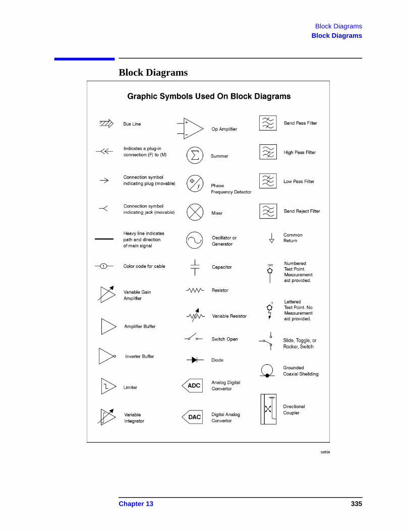
Block Diagrams
Block Diagrams
Block Diagrams
Chapter 13 335

Block Diagrams
Block Diagrams
336 Chapter 13
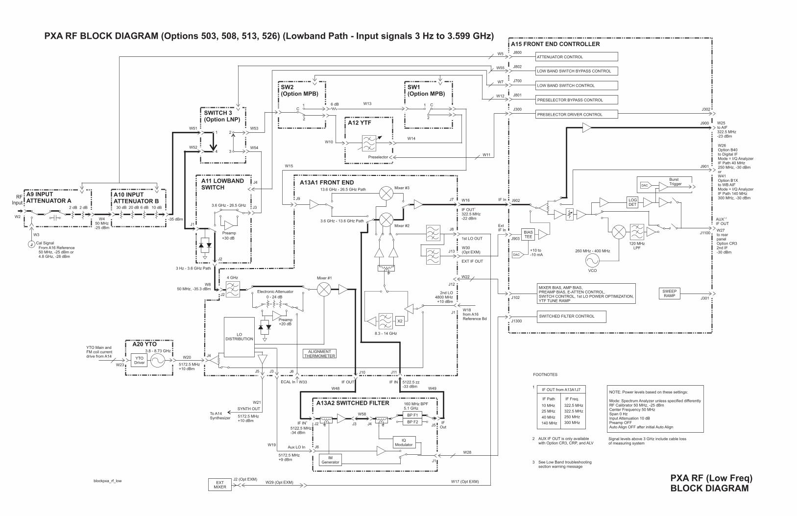
PXA RF BLOCK DIAGRAM (Options 503, 508, 513, 526) (Lowband Path - Input signals 3 Hz to 3.599 GHz)
A9 INPUATTENU
A15 FRONT END CONTROLLER
ED FILTER
YTF
SW1(Option MPB)
1 C
2
Cal SigFrom50 M4.8 G
Path
J7
J8
J13
J1
athMixer #2
Mixer #3
1st LO OUT
2nd LO4800 MHz+10 dBm
W18from A16Reference Bd
260 MHz - 400 MHz
120 MHzLPF
8.3 - 14 GHz
W3
W2
J900
1,2AUX IF OUT
J901
J902IF In
ExtIF In
W16
1IF OUT322.5 MHz-22 dBm
EXT IF OUT
W22
J903
J102 J301
J1300
to AIF322.5 MHz-23 dBm
W25
W26Option B40to Digital IFMode = I/Q AnalyzerIF Path 40 MHz250 MHz, -30 dBmorW41Option B1Xto WB AIFMode = I/Q AnalyzerIF Path 140 MHz300 MHz, -30 dBm
W27to rearpanelOption CR32nd IF-30 dBm
Burst Trigger
J1100
W5
W55
W7
W12
W11
J800
J802
J700
J801
J300 J302
W13
W14
Preselector
J10 J11
ATTENUATOR CONTROL
LOW BAND SWITCH BYPASS CONTROL
LOW BAND SWITCH CONTROL
PRESELECTOR BYPASS CONTROL
PRESELECTOR DRIVER CONTROL
X2
LOGDET
J
RF Input
IQModulator
BP F1
BP F2
VCO
+10 to -10 mA
DAC
DAC
SWITCHED FILTER CONTROL
SWEEPRAMP
IF OUT from A13A1J7NOTE: Power levels based on these settings:
Mode: Spectrum Analyzer unless specified differentlyRF Calibrator 50 MHz, -25 dBmCenter Frequency 50 MHzSpan 0 HzInput Attenuation 10 dBPreamp OFFAuto Align OFF after initial Auto Align
AUX IF OUT is only available with Option CR3, CRP, and ALV
See Low Band troubleshooting section warning message
Signal levels above 3 GHz include cable loss of measuring system
FOOTNOTES
1
2
3
IF Path IF Freq.
10 MHz
25 MHz
40 MHz
140 MHz
322.5 MHz
322.5 MHz
250 MHz
300 MHz
BIASTEE
MIXER BIAS, AMP BIAS, PREAMP BIAS, E-ATTEN CONTROL, SWITCH CONTROL, 1st LO POWER OPTIMIZATION,YTF TUNE RAMP
W58
W49
W28
IF Out
J1
J4 J5
IF IN 5122.5 zz-33 dBm
160 MHz BPF5.1 GHz
J12
W30(Opt EXM)
T ATOR A
A20 YTO
A13A2 SWITCH
A10 INPUT ATTENUATOR B
A11 LOWBAND SWITCH
SWITCH 3(Option LNP)
A12
SW2(Option MPB)
A13A1 FRONT END
30 dB2 dB 2 dB
6 dB1C
2
10 dB
-35 dBm
20 dB 6 dB
0 - 24 dB
+20 dB
nal A16 ReferenceHz, -25 dBm orHz, -28 dBm
13.6 GHz - 26.5 GHz
J9
3.6 GHz - 13.6 GHz P
3.6 GHz - 26.5 GHz
3 Hz - 3.6 GHz Path
4 GHz
+30 dB
Preamp
Preamp
Electronic Attenuator
Mixer #1
3.8 - 8.73 GHz
J1
W450 MHz-25 dBm
W850 MHz, -35.3 dBm
W51 W531
4
2
3W54
W10
W15
W52
J3
J3J5 J6
ALIGNMENTTHERMOMETER
YTO Driver
LO DISTRIBUTION
W19
W21
W33
W48
J2
J4
W20
Aux LO In
J2
J6
J3
W23
YTO Main and FM coil current drive from A14
To A14Synthesizer
ECAL In
3IF IN
IF OUT
5172.5 MHz+10 dBm
5122.5 MHz-34 dBm
5172.5 MHz+9 dBm
SYNTH OUT
5172.5 MHz+10 dBm
J4
IMGenerator
J2
PXA RF (Low Freq) BLOCK DIAGRAM
blockpxa_rf_low J2 (Opt EXM)W29 (Opt EXM)EXT
MIXER
W17 (Opt EXM)
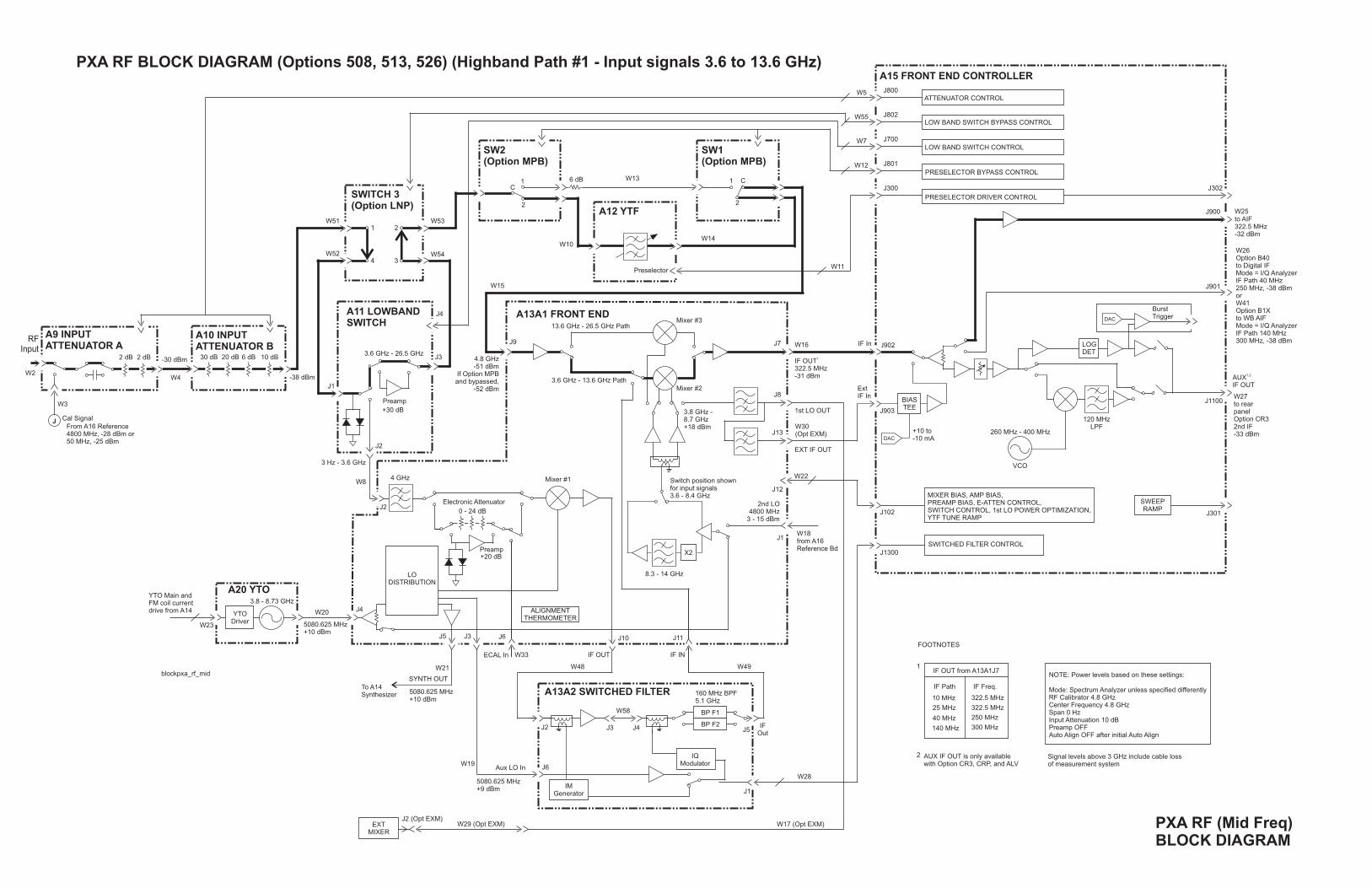
PXA RF BLOCK DIAGRAM (Options 508, 513, 526) (Highband Path #1 - Input signals 3.6 to 13.6 GHz)
A9 INPUATTENU
A15 FRONT END CONTROLLER
YTF
SW1(Option MPB)
1 C
2
Cal SigFrom480050 M
Path
J7
J8
J13
J1
ath
3.8 GHz - 8.7 GHz+18 dBm
1st LO OUT
2nd LO4800 MHz
3 - 15 dBm
Switch position shown for input signals 3.6 - 8.4 GHz
W18from A16Reference Bd
260 MHz - 400 MHz
120 MHzLPF
8.3 - 14 GHz
W3
W2
J900
1,2AUX IF OUT
J901
J902IF In
ExtIF In
W16
1IF OUT322.5 MHz-31 dBm
EXT IF OUT
W22
J903
J102 J301
J1300
to AIF322.5 MHz-32 dBm
W25
W27to rearpanelOption CR32nd IF-33 dBm
Burst Trigger
J1100
W5
W55
W7
W12
W11
J800
J802
J700
J801
J300 J302
W13
W14
Preselector
ATTENUATOR CONTROL
LOW BAND SWITCH BYPASS CONTROL
LOW BAND SWITCH CONTROL
PRESELECTOR BYPASS CONTROL
PRESELECTOR DRIVER CONTROL
X2
LOGDET
J
RF Input
VCO
+10 to -10 mA
DAC
DAC
SWITCHED FILTER CONTROL
IF OUT from A13A1J7NOTE: Power levels based on these settings:
Mode: Spectrum Analyzer unless specified differently RF Calibrator 4.8 GHzCenter Frequency 4.8 GHzSpan 0 HzInput Attenuation 10 dBPreamp OFFAuto Align OFF after initial Auto Align
AUX IF OUT is only available with Option CR3, CRP, and ALV
Signal levels above 3 GHz include cable loss of measurement system
FOOTNOTES
1
2
IF Path IF Freq.
10 MHz
25 MHz
40 MHz
140 MHz
322.5 MHz
322.5 MHz
250 MHz
300 MHz
BIASTEE
MIXER BIAS, AMP BIAS, PREAMP BIAS, E-ATTEN CONTROL, SWITCH CONTROL, 1st LO POWER OPTIMIZATION,YTF TUNE RAMP
J12
W26Option B40to Digital IFMode = I/Q AnalyzerIF Path 40 MHz250 MHz, -38 dBmorW41Option B1Xto WB AIFMode = I/Q AnalyzerIF Path 140 MHz300 MHz, -38 dBm
SWEEPRAMP
ED FILTER
J10 J11
IQModulator
BP F1
BP F2
W58
W49
W28
IF Out
J1
J4 J5
IF IN
160 MHz BPF5.1 GHz
W30(Opt EXM)
Mixer #3
Mixer #2
T ATOR A
A10 INPUT ATTENUATOR B
A11 LOWBAND SWITCH
SWITCH 3(Option LNP)
A12
SW2(Option MPB)
A13A1 FRONT END
30 dB2 dB 2 dB
6 dB1C
2
10 dB-30 dBm
-38 dBm
20 dB 6 dB
0 - 24 dB
nal A16 Reference MHz, -28 dBm orHz, -25 dBm
13.6 GHz - 26.5 GHz
J9
3.6 GHz - 13.6 GHz P
4.8 GHz-51 dBm
If Option MPB and bypassed,
-52 dBm
3.6 GHz - 26.5 GHz
3 Hz - 3.6 GHz
4 GHz
+30 dB
Preamp
Electronic Attenuator
J1
W4
W8
W51 W531
4
2
3W54
W10
W15
W52
J3
J2
J4
blockpxa_rf_mid
J2
A20 YTO
A13A2 SWITCH
+20 dB
3.8 - 8.73 GHz
J3J5 J6
ALIGNMENTTHERMOMETER
YTO Driver
LO DISTRIBUTION
W19
W21
W33
W48
W20
Aux LO In
J2
J6
J3
W23
YTO Main and FM coil current drive from A14
To A14Synthesizer
ECAL In IF OUT
5080.625 MHz+10 dBm
5080.625 MHz+9 dBm
SYNTH OUT
5080.625 MHz+10 dBm
J4
IMGenerator
Preamp
Mixer #1
PXA RF (Mid Freq) BLOCK DIAGRAM
J2 (Opt EXM)W29 (Opt EXM)EXT
MIXERW17 (Opt EXM)

PXA RF BLOCK DIAGRAM (Option 526) (Highband Path #2 - Input signals 13.6 GHz to 26.5 GHz)
A9 INPUATTENU
A15 FRONT END CONTROLLER
ED FILTER
YTF
SW1(Option MPB)
1 C
2
Cal SigFrom4800or50 M
Path
J7
J8
J13
J1
ath
Mixer #3
Mixer #2
8.3 GHz - 14 GHz+18 dBm
1st LO OUT
2nd LO4800 MHz
3 - 15 dBm
Switch position shown for input signals 17 GHz - 26.5 GHz
W18from A16Reference Bd
260 MHz - 400 MHz
120 MHzLPF
8.3 - 14 GHz
W3
W2
J900
1, 2AUX IF OUT
J901
J902IF In
ExtIF In
W16
W30(Opt EXM)
1IF OUT322.5 MHz-37 dBm
EXT IF OUT
W22
J903
J102 J301
J1300
to AIF322.5 MHz-38 dBm
W25
W27to rearpanelOption CR32nd IF-31 dBm
Burst Trigger
J1100
W5
W55
W7
W12
W11
J800
J802
J700
J801
J300 J302
W13
W14
Preselector
J10 J11
ATTENUATOR CONTROL
LOW BAND SWITCH BYPASS CONTROL
LOW BAND SWITCH CONTROL
PRESELECTOR BYPASS CONTROL
PRESELECTOR DRIVER CONTROL
X2
LOGDET
J
RF Input
IQModulator
BP F1
BP F2
VCO
+10 to -10 mA
DAC
DAC
SWITCHED FILTER CONTROL
IF OUT from A13A1J7NOTE: Power levels based on these settings:
Mode: Spectrum Analyzer unless specified differentlyInput Signal 20 GHz, -25 dBmCenter Frequency 20 GHzSpan 0 HzInput Attenuation 10 dBPreamp OFFAuto Align OFF after initial Auto Align
FOOTNOTES
1
IF Path IF Freq.
10 MHz
25 MHz
40 MHz
140 MHz
322.5 MHz
322.5 MHz
250 MHz
300 MHz
BIASTEE
MIXER BIAS, AMP BIAS, PREAMP BIAS, E-ATTEN CONTROL, SWITCH CONTROL, 1st LO POWER OPTIMIZATION
W58
W49
W28
IF Out
J1
J4 J5
IF IN
160 MHz BPF5.1 GHz
J12
AUX IF OUT is only available with Option CR3, CRP, and ALV
Signal levels above 3 GHz include cable loss of measurement system
2
SWEEPRAMP
W26Option B40to Digital IFMode = I/Q AnalyzerIF Path 40 MHz250 MHz, -44 dBmorW41Option B1Xto WB AIFMode = I/Q AnalyzerIF Path 140 MHz300 MHz, -44 dBm
T ATOR A
A20 YTO
A13A2 SWITCH
A10 INPUT ATTENUATOR B
A11 LOWBAND SWITCH
SWITCH 3(Option LNP)
A12
SW2(Option MPB)
A13A1 FRONT END
30 dB2 dB 2 dB
6 dB1C
2
10 dB-28 dBm
-38 dBm
20 dB 6 dB
0 - 24 dB
+20 dB
nal A16 Reference MHz, -28 dBm
Hz, -25 dBm
13.6 GHz - 26.5 GHz
J9
3.6 GHz - 13.6 GHz P
3.6 GHz - 26.5 GHz
3 Hz - 3.6 GHz
4 GHz
+30 dB
Preamp
Mixer #1
Preamp
Electronic Attenuator
3.8 - 8.73 GHz
J1
W4
W8
W51 W531
4
2
3W54
W10
W15
W52
J3
J3J5 J6
ALIGNMENTTHERMOMETER
YTO Driver
LO DISTRIBUTION
W19
W21
W33
W48
J2
J4
W20
Aux LO In
J2
J6
J3
W23
YTO Main and FM coil current drive from A14
To A14Synthesizer
ECAL In IF OUT
5080.625 MHz+10 dBm
5080.625 MHz+9 dBm
SYNTH OUT
5080.625 MHz+10 dBm
J4
IMGenerator
J2
4.8 GHz-59 dBm
If Option MPB and bypassed,
-61 dBm
PXA RF (High Freq) BLOCK DIAGRAM
blockpxa_rf_hiJ2 (Opt EXM)
W29 (Opt EXM)EXTMIXER
W17 (Opt EXM)
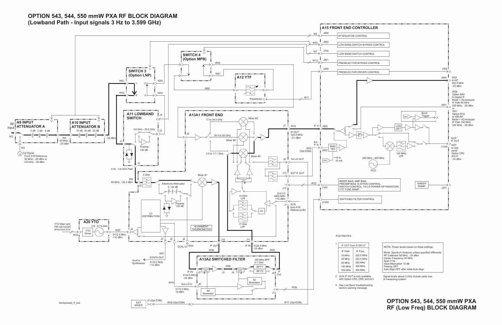
OPTION 543, 544, 550 mmW PXA RF BLOCK DIAGRAM (Lowband Path - Input signals 3 Hz to 3.599 GHz)
A9 INPUATTENU
A15 FRONT END CONTROLLER
ED FILTER
A12 YTF
Cal SigFrom50 M4.8 G
GHz
J7
J8
J13
Mixer #3
Mixer #4
Mixer #21st LO OUT
2nd LO4800 MHz+10 dBm
W18from A16Reference Bd
260 MHz - 400 MHz
120 MHzLPF
14 GHzLPF
17 GHzLPF
W3
W2
J900
1,2AUX IF OUT
J901
J902IF In
ExtIF In
W16
1IF OUT322.5 MHz-21 dBm
EXT IF OUT
W22
W30(Opt EXM) J903
J102 J301
J1300
to AIF322.5 MHz-23 dBm
W25
W26Option B40to Digital IFMode = I/Q AnalyzerIF Path 40 MHz250 MHz, -28 dBmorW41Option B1Xto WB AIFMode = I/Q AnalyzerIF Path 140 MHz300 MHz, -28 dBm
W27to rearpanelOption CR32nd IF-33 dBm
Burst Trigger
J1100
W5
W55
W7
W12
W11
J800
J802
J700
J801
J300 J302
Preselector
J11
ATTENUATOR CONTROL
LOW BAND SWITCH BYPASS CONTROL
LOW BAND SWITCH CONTROL
PRESELECTOR BYPASS CONTROL
PRESELECTOR DRIVER CONTROL
LOGDET
J
RF Input
IQModulator
BP F1
BP F2
VCO
+10 to -10 mA
DAC
DAC
SWITCHED FILTER CONTROL
SWEEPRAMP
IF OUT from A13A1J7NOTE: Power levels based on these settings:
Mode: Spectrum Analyzer unless specified differentlyRF Calibrator 50 MHz, -25 dBmCenter Frequency 50 MHzSpan 0 HzInput Attenuation 10 dBPreamp OFFAuto Align OFF after initial Auto Align
AUX IF OUT is only available with Option CR3, CRP, and ALV
See Low Band troubleshooting section warning message
Signal levels above 3 GHz include cable loss of measuring system
FOOTNOTES
1
2
3
IF Path IF Freq.
10 MHz
25 MHz
40 MHz
140 MHz
160 MHz
322.5 MHz
322.5 MHz
250 MHz
300 MHz
300 MHz
BIASTEE
MIXER BIAS, AMP BIAS, PREAMP BIAS, E-ATTEN CONTROL, SWITCH CONTROL, 1st LO POWER OPTIMIZATION,YTF TUNE RAMP
W58
W49
W28
IF Out
J1
J4 J5
IF IN 5122.5 MHz-33 dBm
160 MHz BPF5.1 GHz
J12
X2
J1
T ATOR A
A20 YTO
A13A2 SWITCH
A10 INPUT ATTENUATOR B
A11 LOWBAND SWITCH
SWITCH 3(Option LNP)
SWITCH 4(Option MPB)
A13A1 FRONT END
20 dB2 dB2 dB 6 dB 10 dB
-35 dBm
30 dB
0 - 24 dB
+20 dB
nal A16 ReferenceHz, -25 dBm orHz, -28 dBm
17 to 34.5 GHz
34.4 to 50 J9
3.6 to 17.1 GHz
3.6 GHz - 26.5 GHz
3 Hz - 3.6 GHz Path
4 GHz
+30 dB
Preamp
Preamp
Electronic Attenuator
Mixer #1
3.8 - 8.73 GHz
J1
W450 MHz, -25 dBm
W850 MHz, -35.3 dBm
W51 W591
4
2
3W54
W62
W61
W60
W52
J3
J3J5 J10J6
ALIGNMENTTHERMOMETER
YTO Driver
LO DISTRIBUTION
W19
W21
W33
W48
J2
J4
W20
Aux LO In
J2
J6
J3
W23
YTO Main and FM coil current drive from A14
To A14Synthesizer
ECAL In
3IF IN
IF OUT
5172.5 MHz+10 dBm
5122.5 MHz-34 dBm
5172.5 MHz+9 dBm
SYNTH OUT
5172.5 MHz+10 dBm
J4
IMGenerator
J2
OPTION 543, 544, 550 mmW PXA RF (Low Freq) BLOCK DIAGRAM
J2 (Opt EXM)W29 (Opt EXM) W17 (Opt EXM)blockpxaopt_rf_low EXT
MIXER
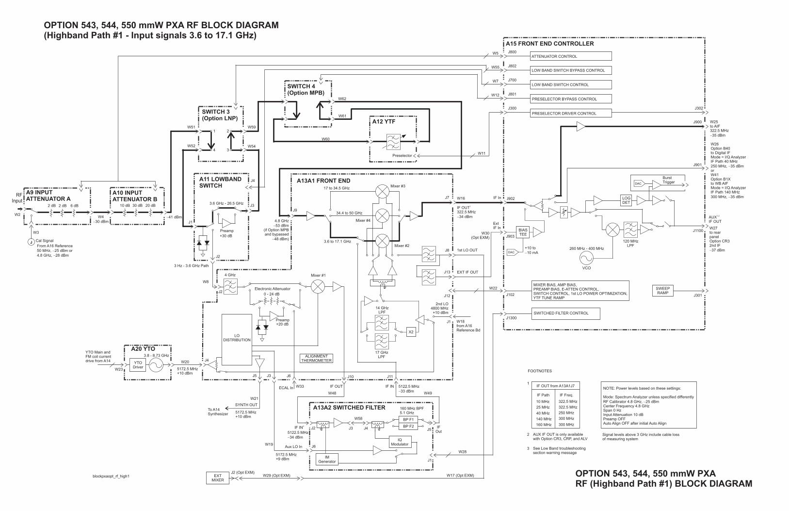
OPTION 543, 544, 550 mmW PXA RF BLOCK DIAGRAM (Highband Path #1 - Input signals 3.6 to 17.1 GHz)
A9 INPUATTENU
A15 FRONT END CONTROLLER
ED FILTER
A12 YTF
Cal Sig
From 50 MH4.8 G
GHz
J7
J8
J13
Mixer #3
Mixer #4
Mixer #21st LO OUT
2nd LO4800 MHz+10 dBm
W18from A16Reference Bd
260 MHz - 400 MHz
120 MHzLPF
14 GHzLPF
17 GHzLPF
W3
W2
J900
1,2AUX IF OUT
J901
J902IF In
ExtIF In
W16
1IF OUT322.5 MHz-34 dBm
EXT IF OUT
W22
W30(Opt EXM) J903
J102 J301
J1300
to AIF322.5 MHz-35 dBm
W25
W26Option B40to Digital IFMode = I/Q AnalyzerIF Path 40 MHz250 MHz, -35 dBmorW41Option B1Xto WB AIFMode = I/Q AnalyzerIF Path 140 MHz300 MHz, -35 dBm
W27to rearpanelOption CR32nd IF-37 dBm
Burst Trigger
J1100
W5
W55
W7
W12
W11
J800
J802
J700
J801
J300 J302
Preselector
J11
ATTENUATOR CONTROL
LOW BAND SWITCH BYPASS CONTROL
LOW BAND SWITCH CONTROL
PRESELECTOR BYPASS CONTROL
PRESELECTOR DRIVER CONTROL
LOGDET
J
RF Input
IQModulator
BP F1
BP F2
VCO
+10 to -10 mA
DAC
DAC
SWITCHED FILTER CONTROL
SWEEPRAMP
IF OUT from A13A1J7NOTE: Power levels based on these settings:
Mode: Spectrum Analyzer unless specified differentlyRF Calibrator 4.8 GHz, -25 dBmCenter Frequency 4.8 GHzSpan 0 HzInput Attenuation 10 dBPreamp OFFAuto Align OFF after initial Auto Align
AUX IF OUT is only available with Option CR3, CRP, and ALV
See Low Band troubleshooting section warning message
Signal levels above 3 GHz include cable loss of measuring system
FOOTNOTES
1
2
3
IF Path IF Freq.
10 MHz
25 MHz
40 MHz
140 MHz
160 MHz
322.5 MHz
322.5 MHz
250 MHz
300 MHz
300 MHz
BIASTEE
MIXER BIAS, AMP BIAS, PREAMP BIAS, E-ATTEN CONTROL, SWITCH CONTROL, 1st LO POWER OPTIMIZATION,YTF TUNE RAMP
W58
W49
W28
IF Out
J1
J4 J5
IF IN 5122.5 MHz-33 dBm
160 MHz BPF5.1 GHz
J12
X2
J1
T ATOR A
A20 YTO
A13A2 SWITCH
A10 INPUT ATTENUATOR B
A11 LOWBAND SWITCH
SWITCH 3(Option LNP)
SWITCH 4(Option MPB)
A13A1 FRONT END
20 dB2 dB2 dB 6 dB 10 dB
-41 dBm
30 dB
0 - 24 dB
+20 dB
nal
A16 Referencez, -25 dBm or
Hz, -28 dBm
17 to 34.5 GHz
34.4 to 50 J9
3.6 to 17.1 GHz
3.6 GHz - 26.5 GHz
3 Hz - 3.6 GHz Path
4 GHz
+30 dB
4.8 GHz-53 dBm
(if Option MPB and bypassed
-48 dBm)
Preamp
Preamp
Electronic Attenuator
Mixer #1
3.8 - 8.73 GHz
J1
W4-30 dBm
W8
W51 W591
4
2
3W54
W62
W61
W60
W52
J3
J3J5 J10J6
ALIGNMENTTHERMOMETER
YTO Driver
LO DISTRIBUTION
W19
W21
W33
W48
J2
J4
W20
Aux LO In
J2
J6
J3
W23
YTO Main and FM coil current drive from A14
To A14Synthesizer
ECAL In
3IF IN
IF OUT
5172.5 MHz+10 dBm
5122.5 MHz-34 dBm
5172.5 MHz+9 dBm
SYNTH OUT
5172.5 MHz+10 dBm
J4
IMGenerator
J2
OPTION 543, 544, 550 mmW PXA RF (Highband Path #1) BLOCK DIAGRAM
J2 (Opt EXM)W29 (Opt EXM) W17 (Opt EXM)blockpxaopt_rf_high1 EXT
MIXER
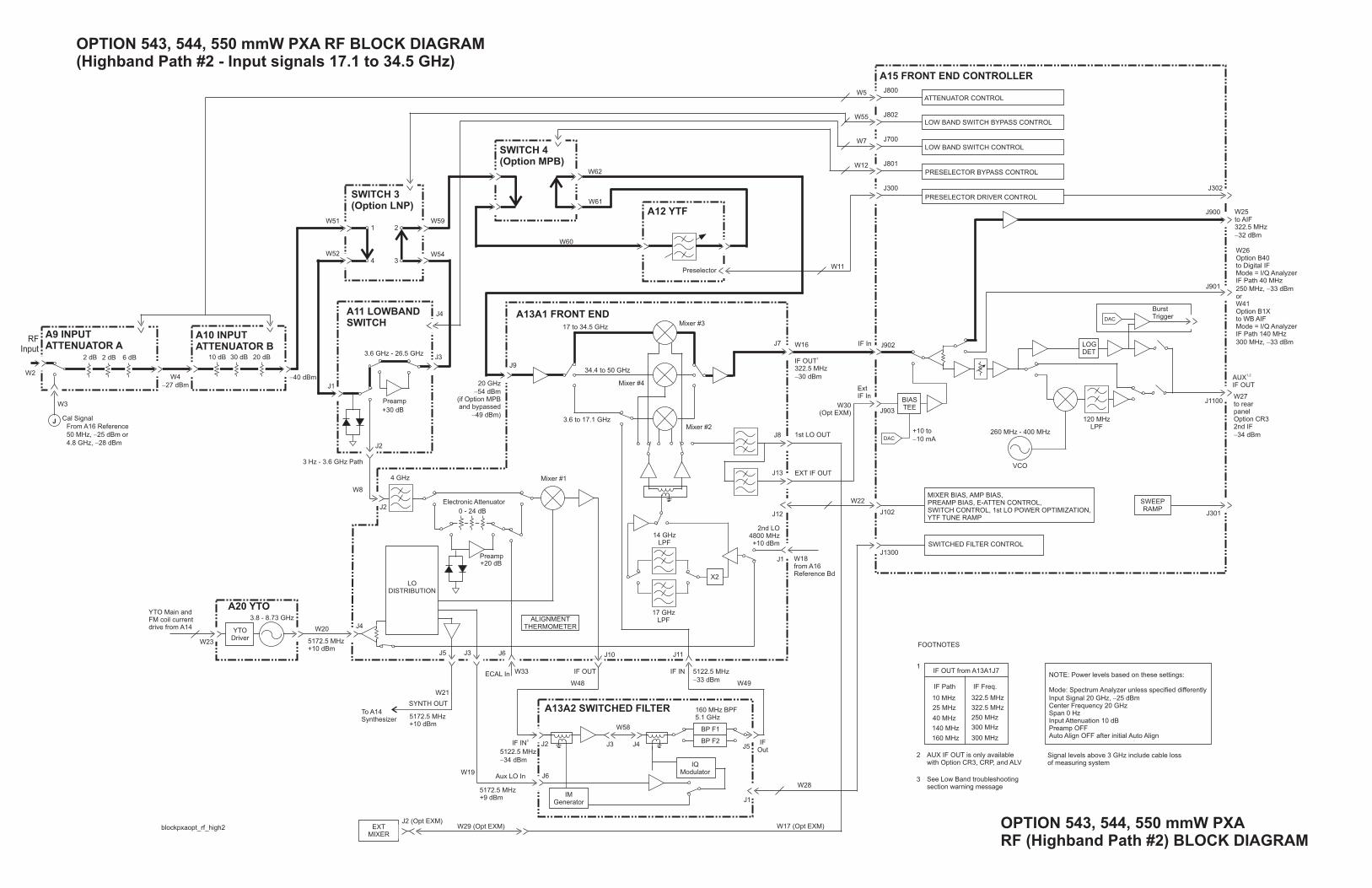
OPTION 543, 544, 550 mmW PXA RF BLOCK DIAGRAM (Highband Path #2 - Input signals 17.1 to 34.5 GHz)
A9 INPUATTENU
A15 FRONT END CONTROLLER
ED FILTER
A12 YTF
Cal SigFrom50 M4.8 G
GHz
J7
J8
J13
Mixer #3
Mixer #4
Mixer #21st LO OUT
2nd LO4800 MHz+10 dBm
W18from A16Reference Bd
260 MHz - 400 MHz
120 MHzLPF
14 GHzLPF
17 GHzLPF
W3
W2
J900
1,2AUX IF OUT
J901
J902IF In
ExtIF In
W16
1IF OUT322.5 MHz-30 dBm
EXT IF OUT
W22
W30(Opt EXM) J903
J102 J301
J1300
to AIF322.5 MHz-32 dBm
W25
W26Option B40to Digital IFMode = I/Q AnalyzerIF Path 40 MHz250 MHz, -33 dBmorW41Option B1Xto WB AIFMode = I/Q AnalyzerIF Path 140 MHz300 MHz, -33 dBm
W27to rearpanelOption CR32nd IF-34 dBm
Burst Trigger
J1100
W5
W55
W7
W12
W11
J800
J802
J700
J801
J300 J302
Preselector
J11
ATTENUATOR CONTROL
LOW BAND SWITCH BYPASS CONTROL
LOW BAND SWITCH CONTROL
PRESELECTOR BYPASS CONTROL
PRESELECTOR DRIVER CONTROL
LOGDET
J
RF Input
IQModulator
BP F1
BP F2
VCO
+10 to -10 mA
DAC
DAC
SWITCHED FILTER CONTROL
SWEEPRAMP
IF OUT from A13A1J7NOTE: Power levels based on these settings:
Mode: Spectrum Analyzer unless specified differentlyInput Signal 20 GHz, -25 dBmCenter Frequency 20 GHzSpan 0 HzInput Attenuation 10 dBPreamp OFFAuto Align OFF after initial Auto Align
AUX IF OUT is only available with Option CR3, CRP, and ALV
See Low Band troubleshooting section warning message
Signal levels above 3 GHz include cable loss of measuring system
FOOTNOTES
1
2
3
IF Path IF Freq.
10 MHz
25 MHz
40 MHz
140 MHz
160 MHz
322.5 MHz
322.5 MHz
250 MHz
300 MHz
300 MHz
BIASTEE
MIXER BIAS, AMP BIAS, PREAMP BIAS, E-ATTEN CONTROL, SWITCH CONTROL, 1st LO POWER OPTIMIZATION,YTF TUNE RAMP
W58
W49
W28
IF Out
J1
J4 J5
IF IN 5122.5 MHz-33 dBm
160 MHz BPF5.1 GHz
J12
X2
J1
T ATOR A
A20 YTO
A13A2 SWITCH
A10 INPUT ATTENUATOR B
A11 LOWBAND SWITCH
SWITCH 3(Option LNP)
SWITCH 4(Option MPB)
A13A1 FRONT END
20 dB2 dB2 dB 6 dB 10 dB
-40 dBm
30 dB
0 - 24 dB
+20 dB
nal A16 ReferenceHz, -25 dBm orHz, -28 dBm
17 to 34.5 GHz
34.4 to 50 J9
3.6 to 17.1 GHz
3.6 GHz - 26.5 GHz
3 Hz - 3.6 GHz Path
4 GHz
+30 dB
Preamp
Preamp
Electronic Attenuator
Mixer #1
3.8 - 8.73 GHz
J1
W4-27 dBm 20 GHz
-54 dBm(if Option MPB and bypassed
-49 dBm)
W8
W51 W591
4
2
3W54
W62
W61
W60
W52
J3
J3J5 J10J6
ALIGNMENTTHERMOMETER
YTO Driver
LO DISTRIBUTION
W19
W21
W33
W48
J2
J4
W20
Aux LO In
J2
J6
J3
W23
YTO Main and FM coil current drive from A14
To A14Synthesizer
ECAL In
3IF IN
IF OUT
5172.5 MHz+10 dBm
5122.5 MHz-34 dBm
5172.5 MHz+9 dBm
SYNTH OUT
5172.5 MHz+10 dBm
J4
IMGenerator
J2
OPTION 543, 544, 550 mmW PXA RF (Highband Path #2) BLOCK DIAGRAM
J2 (Opt EXM)W29 (Opt EXM) W17 (Opt EXM)blockpxaopt_rf_high2 EXT
MIXER
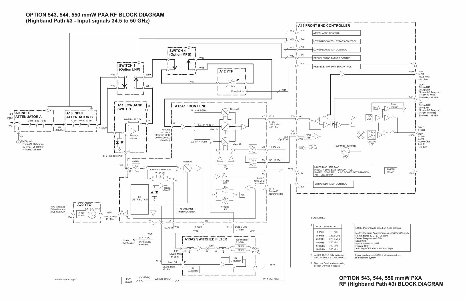
OPTION 543, 544, 550 mmW PXA RF BLOCK DIAGRAM (Highband Path #3 - Input signals 34.5 to 50 GHz)
A9 INPUATTENU
A15 FRONT END CONTROLLER
ED FILTER
A12 YTF
Cal SigFrom50 M4.8 G
GHz
J7
J8
J13
Mixer #3
Mixer #4
Mixer #21st LO OUT
2nd LO4800 MHz+10 dBm
W18from A16Reference Bd
260 MHz - 400 MHz
120 MHzLPF
14 GHzLPF
17 GHzLPF
W3
W2
J900
1,2AUX IF OUT
J901
J902IF In
ExtIF In
W16
1IF OUT322.5 MHz-36 dBm
EXT IF OUT
W22
W30(Opt EXM) J903
J102 J301
J1300
to AIF322.5 MHz-36 dBm
W25
W26Option B40to Digital IFMode = I/Q AnalyzerIF Path 40 MHz250 MHz, -38 dBmorW41Option B1Xto WB AIFMode = I/Q AnalyzerIF Path 140 MHz300 MHz, -38 dBm
W27to rearpanelOption CR32nd IF-32 dBm
Burst Trigger
J1100
W5
W55
W7
W12
W11
J800
J802
J700
J801
J300 J302
Preselector
J11
ATTENUATOR CONTROL
LOW BAND SWITCH BYPASS CONTROL
LOW BAND SWITCH CONTROL
PRESELECTOR BYPASS CONTROL
PRESELECTOR DRIVER CONTROL
LOGDET
J
RF Input
IQModulator
BP F1
BP F2
VCO
+10 to -10 mA
DAC
DAC
SWITCHED FILTER CONTROL
SWEEPRAMP
IF OUT from A13A1J7NOTE: Power levels based on these settings:
Mode: Spectrum Analyzer unless specified differentlyRF Calibrator 40 GHz, -25 dBmCenter Frequency 40 GHzSpan 0 HzInput Attenuation 10 dBPreamp OFFAuto Align OFF after initial Auto Align
AUX IF OUT is only available with Option CR3, CRP, and ALV
See Low Band troubleshooting section warning message
Signal levels above 3 GHz include cable loss of measuring system
FOOTNOTES
1
2
3
IF Path IF Freq.
10 MHz
25 MHz
40 MHz
140 MHz
160 MHz
322.5 MHz
322.5 MHz
250 MHz
300 MHz
300 MHz
BIASTEE
MIXER BIAS, AMP BIAS, PREAMP BIAS, E-ATTEN CONTROL, SWITCH CONTROL, 1st LO POWER OPTIMIZATION,YTF TUNE RAMP
W58
W49
W28
IF Out
J1
J4 J5
IF IN 5122.5 MHz-33 dBm
160 MHz BPF5.1 GHz
J12
X2
J1
T ATOR A
A20 YTO
A13A2 SWITCH
A10 INPUT ATTENUATOR B
A11 LOWBAND SWITCH
SWITCH 3(Option LNP)
SWITCH 4(Option MPB)
A13A1 FRONT END
20 dB2 dB2 dB 6 dB 10 dB
-44 dBm
30 dB
0 - 24 dB
+20 dB
nal A16 ReferenceHz, -25 dBm orHz, -28 dBm
17 to 34.5 GHz
34.4 to 50 J9
3.6 to 17.1 GHz
3.6 GHz - 26.5 GHz
3 Hz - 3.6 GHz Path
40 GHz -61 dBm
(if Option MPBand bypassed,
-54 dBm)
4 GHz
+30 dB
Preamp
Preamp
Electronic Attenuator
Mixer #1
3.8 - 8.73 GHz
J1
W4-33 dBm
W8
W51 W591
4
2
3W54
W62
W61
W60
W52
J3
J3J5 J10J6
ALIGNMENTTHERMOMETER
YTO Driver
LO DISTRIBUTION
W19
W21
W33
W48
J2
J4
W20
Aux LO In
J2
J6
J3
W23
YTO Main and FM coil current drive from A14
To A14Synthesizer
ECAL In
3IF IN
IF OUT
5172.5 MHz+10 dBm
5122.5 MHz-34 dBm
5172.5 MHz+9 dBm
SYNTH OUT
5172.5 MHz+10 dBm
J4
IMGenerator
J2
OPTION 543, 544, 550 mmW PXA RF (Highband Path #3) BLOCK DIAGRAM
J2 (Opt EXM)W29 (Opt EXM) W17 (Opt EXM)blockpxaopt_rf_high3 EXT
MIXER
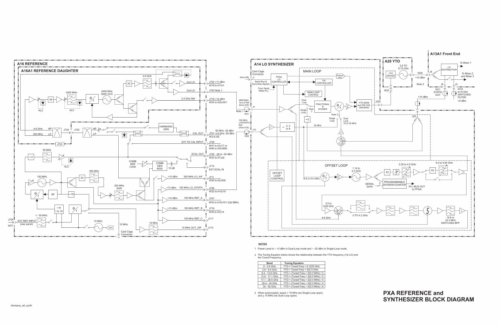
PXA REFERENCE and
blockpxa_ref_syn
A16 RE
A16A
1 (Opt BBA)
or6
1
Note 1
-25 dBm -28 dBm
9 dBm
J704
W37
EXT REF IN
(rear pan
Card CageConnector
A14 LO SYNTHESIZER
MAIN LOOP
OFFSET LOOP
0 TO 4.2 GHz4.8 GHz
3.5 to 9.06 GHz
2.28 to 4.5 GHz
SERIAL DATA PLL MUX OUT
to FPGA
3
4.5 to 9.06 GHz
16.6 or33.3 MHz
SWITCHED BPF
1.14 to 2.3 GHz
3.8 TO8.73 GHz
A20 YTO
A13A1 Front End
J1
J4
J10
FNCONTROLLER
MAIN LOOPCONTROL
(from A8)
W31
4800 MHz1st LO Ref(from A16)
100 MHzLO/SYNTH Ref(from A16)
W32
Serial Bus &Sync/Swp Signals
From Serial Offset PLL
FPGALO
CONTROLLER
PretuneDAC
FRACTIONALN
DIVIDER
YTO MAIN and FM COIL
DRIVERS
Single Loop
50 MHz
Note 3
Note 3
16.6 or 33.3 MHz
Single Loop
DualLoop33 to 55 MHz
DualLoop
LODISTRIBUTION
2, 3or 6
OFFSETLOOP
CONTROL
S
S
IFRF
LO
IFRF
LO
YTO DRIVER
+10 dBm
+10 dBm
+9 dBm
Note 2
W20
W21SYNTH
OUT
J5
J4
J20
J25
W23
J3
W19to A13A2 SWITCHED FILTER
To Mixer 1
To Mixer 2and Mixer 3
f
f
O
O
X2X2
PROGRAMMABLEDIVIDER/COUNTER
S
2
Band Tuning Equation
NOTES
1
3
0 - 3.6 GHz
3.6 - 8.4 GHz
8.4 - 13.6 GHz
13.6 - 17.1 GHz
17.1 - 26.5 GHz
YTO = Tuned Freq + 5.1225 GHz
YTO = Tuned Freq + 322.5 GHz
YTO = (Tuned Freq + 322.5 MHz) / 2
YTO = (Tuned Freq + 322.5 MHz) / 4
YTO = (Tuned Freq + 322.5 MHz) / 2
Power Level is ~ +3 dBm in Dual-Loop mode and ~ -20 dBm in Single-Loop mode.
When autocoupled, spans > 10 MHz are Single-Loop spansand < 10 MHz are Dual-Loop spans.
The Tuning Equation below shows the relationship between the YTO frequency (1st LO) andthe Tuned Frequency.
2
26.4 - 34 GHz YTO = (Tuned Freq + 322.5 MHz) / 4
34 - 50 GHz YTO = (Tuned Freq + 322.5 MHz) / 8
FERENCE
1 REFERENCE DAUGHTER
W18 to A13J1
W3 to A9
W33 to A13J6
W36 to A2J300
EXT ECAL IN
W32 to A14J10
W39 to A3J14
W35 to A19J10
W47 to A3J17 W46 to A25J80
W34 to A25J30
2nd LO
CAL OUT
ECAL OUT
300 MHz LO_AIF
100 MHz LO_SYNTH
+10 dBm
+10 dBm
+13 dBm
+13 dBm
100 MHz REF_A
100 MHz REF_B
100 MHz REF_C
2nd LO
EXT FE CAL INPUT
2.4 GHz Ref
J702 +11 dBm
J725J724
J701
J705
J714
J711
J706
J707
J716
J717
J703 Note 1
J726
J718 +10 dBm
50 MHz 4.8 GHz
-26 to -2
X8
X2
10 MHz
10 MHz
1 - 50 MHz
10 MHz
300 MHzSAW
300 MHz
PUT
el)
100 MHz
2400 MHzSAW VCO
4.8 GHz
2400 MHz
ALC
ALC
ALC
50 MHz
4.8 GHz
300 MHz
HP HP
LP LP
f
fO
fO
O
DAC
HARMONICGEN
COMBGENMOD
COMBSERLVDS
10 dB
J723
2
10
R
NF
1 to 16
Card CageConnector
10 MHz OUT_DIF J710
X3
SYNTHESIZER BLOCK DIAGRAMth
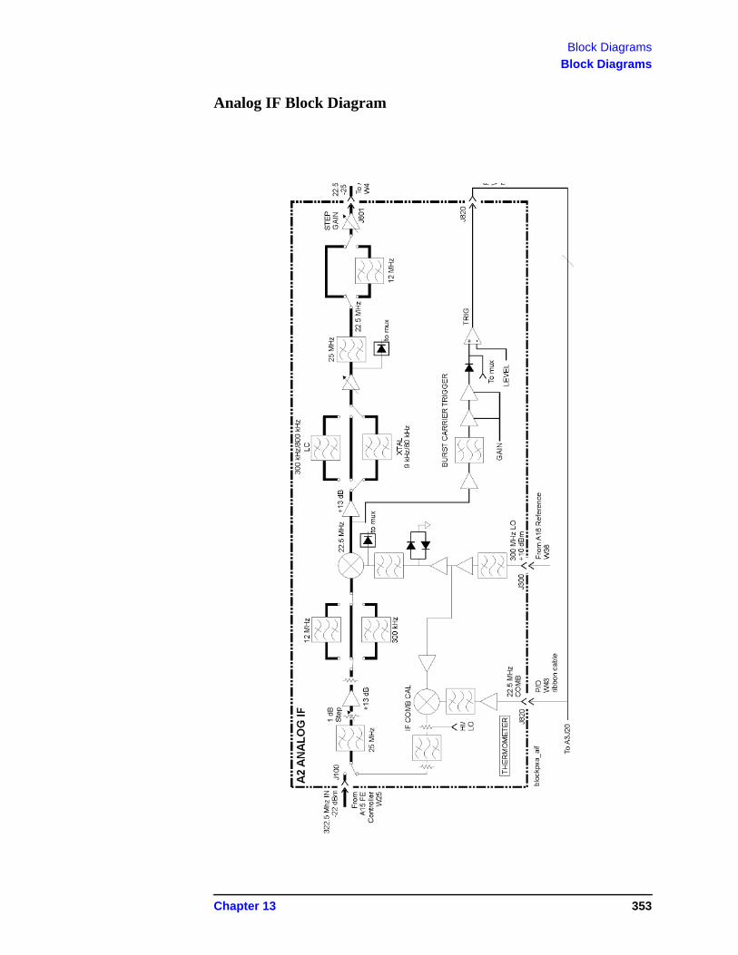
Block Diagrams
Block Diagrams
Analog IF Block Diagram
Chapter 13 353

Block Diagrams
Block Diagrams
354 Chapter 13
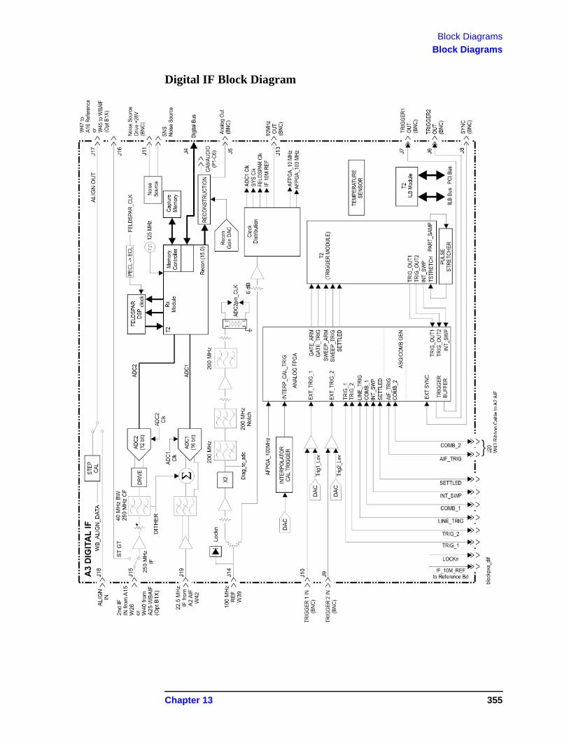
Block Diagrams
Block Diagrams
Digital IF Block Diagram
Chapter 13 355

Block Diagrams
Block Diagrams
356 Chapter 13
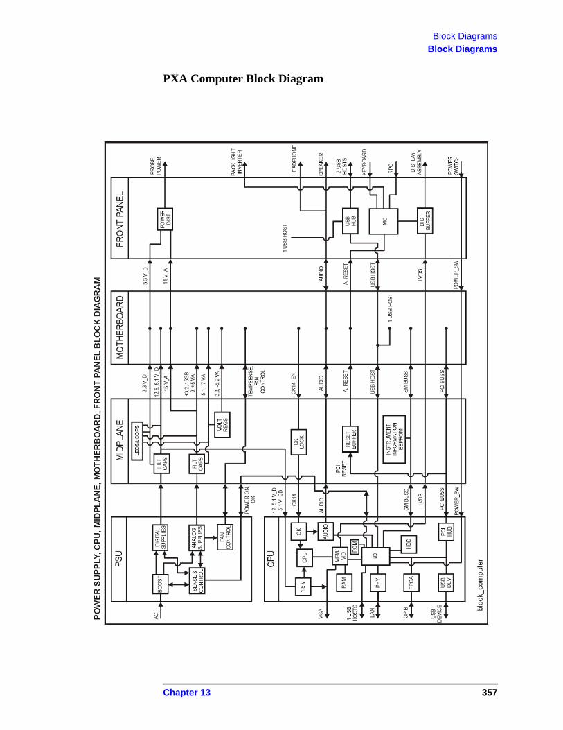
Block Diagrams
Block Diagrams
PXA Computer Block Diagram
Chapter 13 357

Block Diagrams
Block Diagrams
358 Chapter 13
14 Service and Diagnostics Menus
359
Service and Diagnostics Menus
Overview
Overview
The Service capabilities described below are accessed via the Service and Diagnostic menus in the System menu. The Service capabilities are intended for field service technicians. These technicians may be at an Agilent Service Center or at a self-maintaining customer site.
There are two types of Service capabilities:
1. Diagnostics - These are available to any user and will assist in initial troubleshooting of instrument malfunctions. Examples are the ability to read the mechanical relay cycles.
2. Service Functions - These are for use by the factory or field repair technicians, access is controlled. Examples are the ability to band lock the analyzer and control the DAC which sets the 10 MHz Reference frequency.
Controlling Access
There are two levels of service and diagnostics capabilities:
1. “Regular access” to diagnostic capabilities that everyone is allowed access. Care may be required to use a feature appropriately. This is the “Diagnostic” type of Service capability defined above.
2. “Secure service access” to the Service menu. This prevents the casual user from accessing and using these features. It is intended to provide this access to Agilent Service Centers or any customer who purchases the Service Guide. The “Service Functions” type of Service capability is defined above.
To access secured service capabilities the technician is required to enter a specific numeric Service Code that is controlled by the instrument software. The Service Code is defined to be easily entered via the front panel; an external keyboard or mouse will not be required. Once access has been gained, it persists within the execution of the instrument application. If the user exits the instrument application, they must re-enter the Service Code to gain access.
360 Chapter 14
Service and Diagnostics Menus
Overview
Secure service access
To access the secure service capabilities press System, More, Service with the instrument application running. At this point you will see the window shown in Figure 14-1. Enter the Service Code and press Enter.
The Service Code is: -2061
Figure 14-1 Service Code Entry
Chapter 14 361
Ch
apter 14
36
2
Se
rvice an
d D
iag
nostics M
enu
s
Me
nu
s
Service Diagnostics
More
Diagnostics
Service
2 of 2
Menus
Service (in System menu)
Timebase
Timebase DAC1960
Save
†
Service Alignments
LO Bandlock
Off
Band 0
Band 1
Band 2
Band 3
Corrections
LO
Band Lock
Nulling
Band Lock(-1 for no lock)
-1
Lock Funcs
Low Noise
PathNormal
Nulling
More
Timebase
Service
Corrections
Lock
Functions
Align
LO
Control
1 of 2
LO Control
Second LO
Gain DAC0
Ext LO Turnoff
(2 for unlock)0
This menu is onlyavailable on the FactoryImage or with specificlogins, some logins
require a Service Guidefor entry
TG Band Lock(-1 for no lock)
-1
Lock On
Normal
Low Noise Path
Lock Off
Service and Diagnostics Menus
Menus
Corrections Corrections
RF Flatness
IF Flatness
On Off
Snapshot
On Off
RF Flatness
Flatness
Video Shift
On OffTemperature
Gain & Tilt
On Off
Nulling
On OffIntermod
On Off
Nulling
IQ Freq Resp
On Off
IQ Gain
On Off
LO Feedthru
Chapter 14 363
Service and Diagnostics Menus
Menus
Service Alignments
Diagnostics
Align
SubsystemAlign Log...
Visible Align
On Off
Diagnostics
Align Log Mode
Clear Append
Subsystem
ADC
LO
IFRF
Current
System Gain
Current IF
Flatness
IF IF
LO
Phase Noise
Adjustment
364 Chapter 14
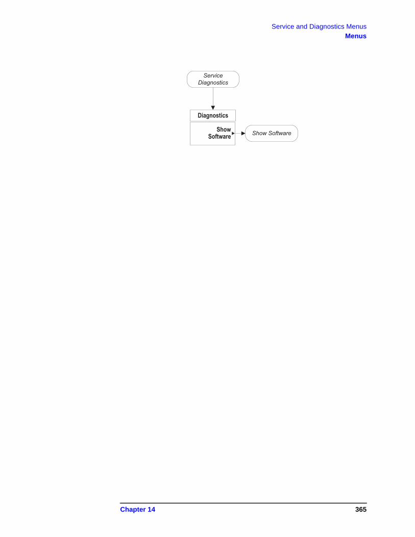
Service and Diagnostics Menus
Menus
Service Diagnostics
Diagnostics
Show Software Show Software
Chapter 14 365
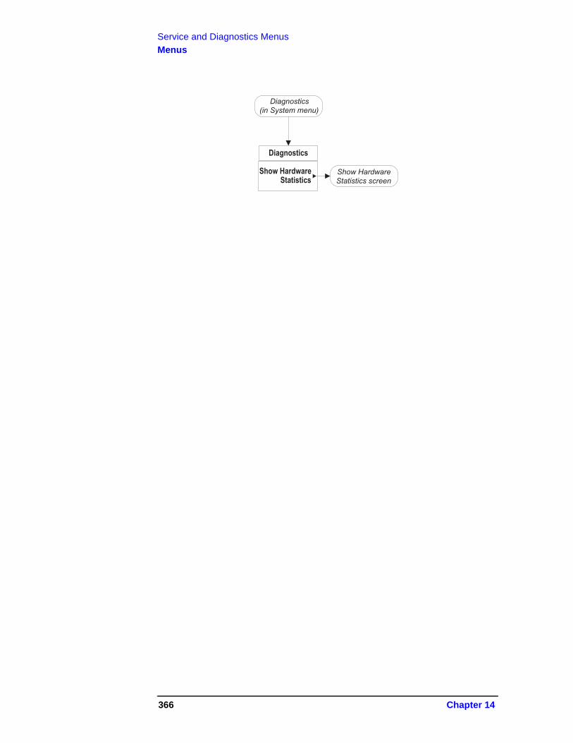
Service and Diagnostics Menus
Menus
Diagnostics(in System menu)
Diagnostics
Show Hardware Statistics
Show HardwareStatistics screen
366 Chapter 14
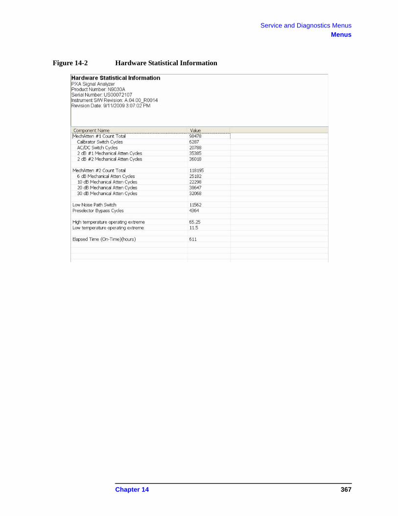
Service and Diagnostics Menus
Menus
Figure 14-2 Hardware Statistical Information
Chapter 14 367
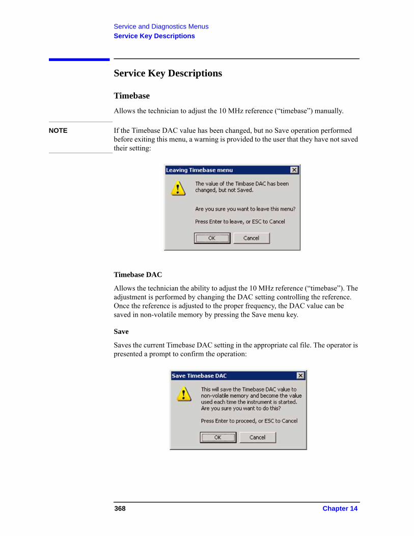
Service and Diagnostics Menus
Service Key Descriptions
Service Key Descriptions
Timebase
Allows the technician to adjust the 10 MHz reference (“timebase”) manually.
NOTE If the Timebase DAC value has been changed, but no Save operation performed before exiting this menu, a warning is provided to the user that they have not saved their setting:
Timebase DAC
Allows the technician the ability to adjust the 10 MHz reference (“timebase”). The adjustment is performed by changing the DAC setting controlling the reference. Once the reference is adjusted to the proper frequency, the DAC value can be saved in non-volatile memory by pressing the Save menu key.
Save
Saves the current Timebase DAC setting in the appropriate cal file. The operator is presented a prompt to confirm the operation:
368 Chapter 14
Service and Diagnostics Menus
Service Key Descriptions
Corrections
The Corrections menu allows the technician to activate and deactivate specific amplitude correction sets. With this capability, the technician can determine if an anomaly is a result of raw hardware performance or incorrect correction data. It also allows the technician the ability to measure the raw hardware performance when all corrections are set to Off.
RF Flatness
Displays a menu which allows the technician to activate and deactivate the corrections unique to the RF flatness of the analyzer. RF Flatness corrections consist of two major parts: raw flatness corrections and temperature corrections. These corrections are summed together and applied by using RF gain, IF gain, and/or “video shift” (post-digitized mathematical offset). The selections in this menu allow the corrections to be applied or not applied to facilitate troubleshooting the cause of flatness-related problems.
Flatness Video Shift On/Off
The Flatness Video Shift turns off the corrections for gain vs. frequency. It does not turn off the corrections for changes in the analog IF gain that accompany flatness changes. This function turns both the gain and video shift on or off, but does not affect the temperature corrections. When set to off, it is possible to measure the raw flatness of the spectrum analyzer while maintaining the temperature corrections.
When Flatness Video Shift is Off, the Advisory Event “Flatness Video Shift OFF” will be displayed.
When Flatness Video Shift is ON, the Advisory Event “Flatness Video Shift OFF” will be cleared.
Temperature Gain & Tilt On/Off
This function controls both temperature adjustment mechanisms: overall gain vs. temperature, and the temperature-proportional tilt of the gain vs. frequency.
When Temperature Gain & Tilt is OFF, the Advisory Event “Flatness Temperature Gain & Tilt OFF” will be displayed.
When Temperature Gain & Tilt is ON, the Advisory Event “Flatness Temperature Gain & Tilt OFF” will be cleared.
Chapter 14 369
Service and Diagnostics Menus
Service Key Descriptions
IF Flatness
This function turns the corrections related to IF flatness On or Off.
When IF Flatness is OFF, the Advisory Event “IF Flatness corrections OFF” will be displayed.
When IF Flatness is ON, the Advisory Event “IF Flatness corrections OFF” will be cleared.
Snapshot Alignments On/Off
During normal auto alignment operation, the firmware will perform an RBW and IQ alignment when the analyzer RBW state is changed, and every 10 minutes thereafter. These alignments can hinder troubleshooting the analyzer since they can change correction factors when the state is changed. Turning snapshot alignments off disables the RBW portion of these alignments for more accurate troubleshooting. (Use IF Flatness ON/OFF to control the IQ alignment.)
When Snapshot Alignments are OFF, the Advisory Event “Snapshot OFF” will be displayed.
When Snapshot Alignments are ON, the Advisory Event “Snapshot OFF” will be cleared.
I/Q Freq Response
This function turns the corrections related to I/Q Frequency Response On or Off. This is only available with the Baseband Analog I/Q option (BBA).
When I/Q Frequency Response is OFF, the Advisory Event “I/Q Freq Response corrections OFF” will be displayed.
When I/Q Frequency Response is ON, the Advisory Event “I/Q Freq Response corrections OFF” will be cleared.
I/Q Gain
This function turns the corrections related to I/Q Gain On or Off. This is only available with the Baseband Analog I/Q option (BBA).
When I/Q Gain is OFF, the Advisory Event “I/Q Gain corrections OFF” will be displayed.
When I/Q Gain is ON, the Advisory Event “I/Q Gain corrections OFF” will be cleared.
370 Chapter 14
Service and Diagnostics Menus
Service Key Descriptions
Band Lock
Provides the ability to tune the analyzer over as large a range as can be accommodated by the specified harmonic number and 1st LO frequency range. As a result, this feature can be used to check performance in the frequency band overlap regions. By definition, multi-band sweeps are not allowed.
When band lock is in effect the Advisory Event “Band Locked: Band <x>” where “x” is a value between 0 and 6.
When band lock is not in affect the Advisory Event “Band Locked: Band <x>” is cleared.
Dependencies/Couplings:
1. Band Lock is only available on analyzers with frequency range options beyond 3.6 GHz
2. The individual bands available for selection also depends upon the particular frequency range option.
Off
Turns Band Lock to Off. Analyzer will tune from band to band normally.
Band 0
Locks the analyzer to Band 0.
Band 1
Locks the analyzer to Band 1.
Band 2
Locks the analyzer to Band 2.
Band 3
Locks the analyzer to Band 3.
Band 4
Locks the analyzer to Band 4.
Band 5
Locks the analyzer to Band 5.
Band 6
Locks the analyzer to Band 6. The Band 6 key label can be different depending on which option is installed.
Chapter 14 371
Service and Diagnostics Menus
Service Key Descriptions
LO Band Lock
Provides the ability to tune the analyzer over as large a range as can be accommodated by the specified LO Band. As a result, this feature can be used to check performance in the LO band overlap regions. By definition, multi-band sweeps are not allowed.
When band lock is in effect the Advisory Event “LO Band Locked: Band <x>” where “x” is a value between 0 and 6.
When band lock is not in affect the Advisory Event “LO Band Locked: Band <x>” is cleared.
Dependencies/Couplings:
LO Bandlock will be grayed-out if Bandlock is OFF. If Harmonic Bandlock is any setting other than OFF, LO Bandlock menu key is enabled. If LO Bandlock is other than OFF, and the Harmonic Bandlock is transitioned to OFF, the LO Bandlock is set to OFF.
Off
Turns LO Band Lock to Off. Analyzer will tune from LO band to LO band normally.
Band 0
Locks the analyzer to LO Band 0.
Band 1
Locks the analyzer to LO Band 1.
Band 2
Locks the analyzer to LO Band 2.
Band 3
Locks the analyzer to LO Band 3.
372 Chapter 14
Service and Diagnostics Menus
Service Key Descriptions
Low Noise Path
Provides the ability to lock the Option (LNP) Low Noise Path switch that is used in the μWave Path Control menu into the ON position, regardless of the state of the μWave Path Control menu or functions. The low noise path flatness corrections are applied.
NOTE In normal operation the Low Noise Path and the Microwave Preselector Bypass (Option MPB) cannot be turned on at the same time. This is done to protect the highband mixer from excessive power.
WARNING Assure the mixer power is < −10 dBm (mixer power = input power - input attenuation)
LO Control
Provides keys that allow you to control the LO. This is only present on analyzers equipped with Opt EXM, External Mixing.
2nd LO Gain DAC
This parameter provides the ability to adjust the output gain of the 2nd LO DAC. The range is from 0 to 4095 where 0 is the minimum gain and 4095 is the maximum gain. Setting a value of 4096 or greater returns control to the instrument. In External Mixing, this DAC controls the level of the 1st LO signal at the front panel EXT MIXER connector.
External LO Turnoff
Disconnects the 1st LO path which will minimize the effect of the 1st LO signal at the front panel EXT MIXER connector.
Chapter 14 373

Service and Diagnostics Menus
Service Key Descriptions
Align
The Align Menu allows accessing Diagnostic capabilities of Alignment, and invoking alignments for individual subsystems.
Diagnostic
The Diagnostic menu contains items for controlling the operating behavior of Alignment and the Alignment reporting capabilities.
Visible Align
Controls the state of Visible Align. Visible Align replaces the “Aligning 1 or X” messages with descriptive messages describing the alignment piece begin executed.
Align Log…
Invokes Notepad with the Alignment Log loaded. The log can be viewed or saved to an external media or drive. Notepad can be closed without a mouse or external keyboard by pressing ALT front-panel key, then arrow down to highlight Exit, then press Enter.
Align Log Mode
The Alignment System places information about the last alignment performed into a log. The log can be configured to operate in clear or append mode. In clear mode the log only contains information on the last alignment performed; the log is cleared with each alignment performed. In append mode each new alignment appends to the log. In append mode, care must be taken by the operator to not allow the log to grow to a size so large as to inhibit system operation.
Subsystem
The Subsystem menu allows invoking individual components of the internal alignments.
ADC
Immediately executes an alignment of the ADC subsystem. The instrument will stop any measurement currently underway, perform the alignment, then restart the measurement from the beginning.
A failure of ADC will set the Error Condition “Align ADC failed”. A failure will not employ new ADC alignment data.
Successful completion of ADC will clear the Error Condition “Align ADC failed”.
The Advisory Event “Alignment complete” is displayed when the alignment is complete.
Align ADC can be interrupted by pressing the Cancel (ESC) front-panel key. When this occurs, no new ADC alignment data will be employed.
374 Chapter 14
Service and Diagnostics Menus
Service Key Descriptions
LO
Immediately executes an alignment of the LO subsystem. The instrument will stop any measurement currently underway, perform the alignment, then restart the measurement from the beginning.
A failure of LO will set the Error Condition “Align LO failed”. A failure will not employ new LO alignment data.
Successful completion of LO will clear the Error Condition “Align LO failed”.
The Advisory Event “Alignment complete” is displayed when the alignment is complete.
Align LO can be interrupted by pressing the Cancel (ESC) front-panel key. When this occurs, no new LO alignment data will be employed.
IF
Immediately executes an alignment of the IF subsystem. The instrument will stop any measurement currently underway, perform the alignment, then restart the measurement from the beginning.
A failure of IF will set the Error Condition “Align IF failed”. A failure will not employ new IF alignment data.
Successful completion of IF will clear the Error Condition “Align IF failed” and clear bit 6 in the Status.
The Advisory Event “Alignment complete” is displayed when the alignment is complete.
Align IF can be interrupted by pressing the Cancel (ESC) front-panel key. When this occurs, no new IF alignment data will be employed.
Current IF Flatness
Immediately executes an alignment of the Current IF Flatness, for the purpose of improving the absolute amplitude accuracy within FFT Sweeps and improving the group delay in some digital demodulation measurements. The instrument will stop any measurement currently underway, perform the alignment, then restart the measurement from the beginning.
The Advisory Event “Alignment complete” is displayed when the alignment is complete.
Align Current IF Flatness can be interrupted by pressing the Cancel (ESC) front-panel key. When this occurs, no new Current IF Flatness alignment data will be employed.
RF
This is exactly the same as the customer accessible Align Now, RF with one exception: the alignment can be invoked even if a previous Align Now, All has not been executed (this key is not grayed-out if using default alignment data). See description of Align Now, RF in the User's Guide.
Chapter 14 375
Service and Diagnostics Menus
Service Key Descriptions
Current System Gain
Immediately executes an alignment of the Current System Gain, for the purpose of improving small amplitude variations that occur as resolution bandwidth is switched. This alignment is done by measuring the response of the current system state configuration to the 50 MHz amplitude reference signal. All subsequent measurements are then compensated appropriately for absolute amplitude accuracy. The instrument will stop any measurement currently underway, perform the alignment, then restart the measurement from the beginning.
The Advisory Event “Alignment complete” is displayed when the alignment is complete.
Align Current System Gain can be interrupted by pressing the Cancel (ESC) front-panel key. When this occurs, no new Current System Gain alignment data will be employed.
LO Phase Noise Adjustment
Immediately executes an optimization for LO Phase Noise. When the optimization is finished the value is stored in non-volatile memory. The instrument will stop any measurement currently underway, perform the alignment, and then restart the measurement from the beginning (similar to pressing the Restart key).
Nulling
The hardware is capable of nulling (cancelling) the LO Feedthru, intermodulation products, or neither. It is physically not capable of nulling both at the same time.
LO Feedthru Nulling
Control is available to set the state of LO Feedthru nulling ON or OFF. In the ON state, the software will determine when it is appropriate to null the LO Feedthru. LO nulling is only available in low band.
Intermod Nulling
Control is available to set the state of Intermod Nulling On or OFF. In the ON state, the software will determine when it is appropriate to null the intermodulation products. IM nulling is only available in low band.
Diagnostics
Pressing Diagnostics in the Service Menu brings up the Service Diagnostics submenu. The functions in this menu allow the technician to do more detailed, lower-level troubleshooting.
376 Chapter 14
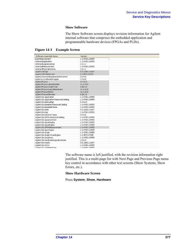
Service and Diagnostics Menus
Service Key Descriptions
Show Software
The Show Software screen displays revision information for Agilent internal software that comprises the embedded application and programmable hardware devices (FPGAs and PLDs).
Figure 14-3 Example Screen
The software name is left justified, with the revision information right justified. This is a multi-page list with Next Page and Previous Page menu key control in accordance with other text screens (Show Systems, Show Errors, etc.).
Show Hardware Screen
Press System, Show, Hardware
Chapter 14 377

Service and Diagnostics Menus
Service Key Descriptions
378 Chapter 14
15 Replaceable Parts
379
Replaceable Parts
What You Will Find in This Chapter
What You Will Find in This Chapter
The following information is found in this chapter:
1. Part number tables for assemblies, mechanical parts, cables, front panel connectors, and labels.
2. Part location diagrams for the following:
Fig. 15-1 Major Assemblies page 397
Fig. 15-2 External Hardware page 398
Fig. 15-3 CPU Assembly page 399
Fig. 15-4 Disk Drive Tray Assembly page 400
Fig. 15-5 Top Brace and Reference Bracket page 401
Fig. 15-6 RF Area (Options 503, 508, 513, 526) page 402
Fig. 15-7 RF Area (Options 543, 544, 550) page 404
Fig. 15-8 Front End Parts (Options 503, 508, 513, 526) page 406
Fig. 15-9 Front End Parts (Options 543, 544, 550) page 407
Fig. 15-10 Front End Cables page 408
Fig. 15-11 Reference Board Cables page 409
Fig. 15-12 AIF Cables page 410
Fig. 15-13 DIF Cables page 410
Fig. 15-14 AIF/DIF Assemblies page 412
Fig. 15-15 Motherboard page 413
Fig. 15-16 Chassis page 414
Fig. 15-17 Fan Hardware page 416
Fig. 15-18 Input Connector page 417
Fig. 15-19 Front Frame Parts - LCD page 418
Fig. 15-20 Front Frame Parts (shields off) - LCD page 419
Fig. 15-21 Front Frame Parts - LED page 420
Fig. 15-22 Front Frame Parts (shields off) - LED page 421
Fig. 15-23 Front Frame Exploded View - LCD page 422
Fig. 15-24 Front Frame Exploded View - LED page 424
380 Chapter 15
Replaceable Parts
What You Will Find in This Chapter
How to Order Parts
To order an assembly or mechanical part listed in this chapter, go to:
www.parts.agilent.com
If you do not have web access, or the parts you are interested in cannot be found in the parts list provided, contact your local Agilent Technologies sales and service office with the following information:
• Product model number• Product serial number• Description of where the part is located, what it looks like,
and its function (if known)• Quantity required
For a list of Agilent Technologies sales and service office locations, refer to “Contacting Agilent Technologies” on page 41.
Chapter 15 381
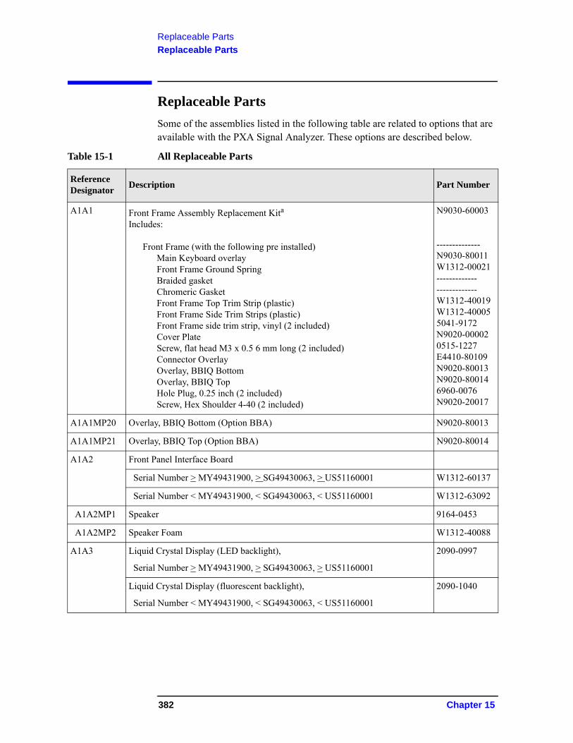
Replaceable Parts
Replaceable Parts
Replaceable Parts
Some of the assemblies listed in the following table are related to options that are available with the PXA Signal Analyzer. These options are described below.
Table 15-1 All Replaceable Parts
Reference Designator
Description Part Number
A1A1 Front Frame Assembly Replacement Kita
Includes:
Front Frame (with the following pre installed)Main Keyboard overlay Front Frame Ground SpringBraided gasketChromeric GasketFront Frame Top Trim Strip (plastic) Front Frame Side Trim Strips (plastic)Front Frame side trim strip, vinyl (2 included)
Cover Plate Screw, flat head M3 x 0.5 6 mm long (2 included) Connector Overlay
Overlay, BBIQ Bottom Overlay, BBIQ Top
Hole Plug, 0.25 inch (2 included)Screw, Hex Shoulder 4-40 (2 included)
N9030-60003
--------------N9030-80011W1312-00021--------------------------W1312-40019W1312-400055041-9172N9020-000020515-1227E4410-80109N9020-80013N9020-800146960-0076N9020-20017
A1A1MP20 Overlay, BBIQ Bottom (Option BBA) N9020-80013
A1A1MP21 Overlay, BBIQ Top (Option BBA) N9020-80014
A1A2 Front Panel Interface Board
Serial Number > MY49431900, > SG49430063, > US51160001 W1312-60137
Serial Number < MY49431900, < SG49430063, < US51160001 W1312-63092
A1A2MP1 Speaker 9164-0453
A1A2MP2 Speaker Foam W1312-40088
A1A3 Liquid Crystal Display (LED backlight),
Serial Number > MY49431900, > SG49430063, > US51160001
2090-0997
Liquid Crystal Display (fluorescent backlight),
Serial Number < MY49431900, < SG49430063, < US51160001
2090-1040
382 Chapter 15
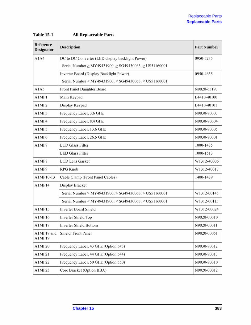
Replaceable Parts
Replaceable Parts
A1A4 DC to DC Converter (LED display backlight Power)
Serial Number > MY49431900, > SG49430063, > US51160001
0950-5235
Inverter Board (Display Backlight Power)
Serial Number < MY49431900, < SG49430063, < US51160001
0950-4635
A1A5 Front Panel Daughter Board N9020-63193
A1MP1 Main Keypad E4410-40100
A1MP2 Display Keypad E4410-40101
A1MP3 Frequency Label, 3.6 GHz N9030-80003
A1MP4 Frequency Label, 8.4 GHz N9030-80004
A1MP5 Frequency Label, 13.6 GHz N9030-80005
A1MP6 Frequency Label, 26.5 GHz N9030-80001
A1MP7 LCD Glass Filter 1000-1435
LED Glass Filter 1000-1513
A1MP8 LCD Lens Gasket W1312-40006
A1MP9 RPG Knob W1312-40017
A1MP10-13 Cable Clamp (Front Panel Cables) 1400-1439
A1MP14 Display Bracket
Serial Number > MY49431900, > SG49430063, > US51160001 W1312-00145
Serial Number < MY49431900, < SG49430063, < US51160001 W1312-00115
A1MP15 Inverter Board Shield W1312-00024
A1MP16 Inverter Shield Top N9020-00010
A1MP17 Inverter Shield Bottom N9020-00011
A1MP18 and A1MP19
Shield, Front Panel N9020-00051
A1MP20 Frequency Label, 43 GHz (Option 543) N9030-80012
A1MP21 Frequency Label, 44 GHz (Option 544) N9030-80013
A1MP22 Frequency Label, 50 GHz (Option 550) N9030-80010
A1MP23 Core Bracket (Option BBA) N9020-00012
Table 15-1 All Replaceable Parts
Reference Designator
Description Part Number
Chapter 15 383
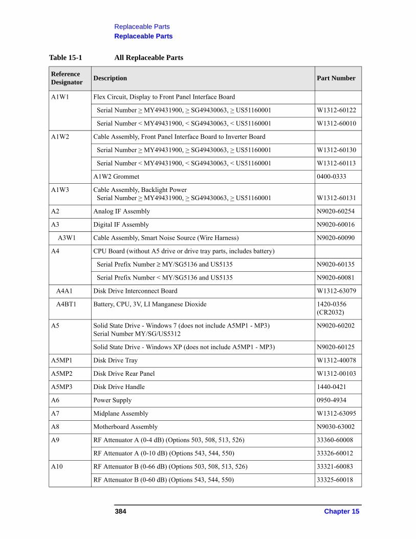
Replaceable Parts
Replaceable Parts
A1W1 Flex Circuit, Display to Front Panel Interface Board
Serial Number > MY49431900, > SG49430063, > US51160001 W1312-60122
Serial Number < MY49431900, < SG49430063, < US51160001 W1312-60010
A1W2 Cable Assembly, Front Panel Interface Board to Inverter Board
Serial Number > MY49431900, > SG49430063, > US51160001 W1312-60130
Serial Number < MY49431900, < SG49430063, < US51160001 W1312-60113
A1W2 Grommet 0400-0333
A1W3 Cable Assembly, Backlight PowerSerial Number > MY49431900, > SG49430063, > US51160001 W1312-60131
A2 Analog IF Assembly N9020-60254
A3 Digital IF Assembly N9020-60016
A3W1 Cable Assembly, Smart Noise Source (Wire Harness) N9020-60090
A4 CPU Board (without A5 drive or drive tray parts, includes battery)
Serial Prefix Number ≥ MY/SG5136 and US5135 N9020-60135
Serial Prefix Number < MY/SG5136 and US5135 N9020-60081
A4A1 Disk Drive Interconnect Board W1312-63079
A4BT1 Battery, CPU, 3V, LI Manganese Dioxide 1420-0356(CR2032)
A5 Solid State Drive - Windows 7 (does not include A5MP1 - MP3)Serial Number MY/SG/US5312
N9020-60202
Solid State Drive - Windows XP (does not include A5MP1 - MP3) N9020-60125
A5MP1 Disk Drive Tray W1312-40078
A5MP2 Disk Drive Rear Panel W1312-00103
A5MP3 Disk Drive Handle 1440-0421
A6 Power Supply 0950-4934
A7 Midplane Assembly W1312-63095
A8 Motherboard Assembly N9030-63002
A9 RF Attenuator A (0-4 dB) (Options 503, 508, 513, 526) 33360-60008
RF Attenuator A (0-10 dB) (Options 543, 544, 550) 33326-60012
A10 RF Attenuator B (0-66 dB) (Options 503, 508, 513, 526) 33321-60083
RF Attenuator B (0-60 dB) (Options 543, 544, 550) 33325-60018
Table 15-1 All Replaceable Parts
Reference Designator
Description Part Number
384 Chapter 15
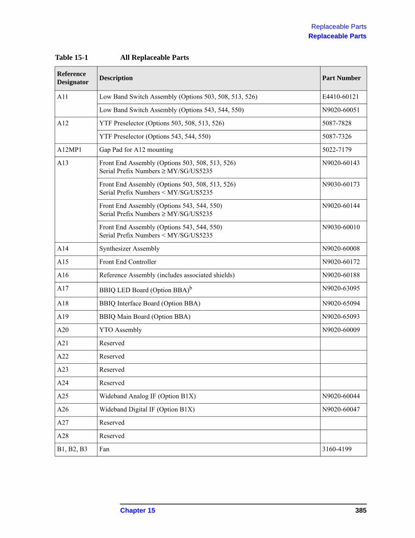
Replaceable Parts
Replaceable Parts
A11 Low Band Switch Assembly (Options 503, 508, 513, 526) E4410-60121
Low Band Switch Assembly (Options 543, 544, 550) N9020-60051
A12 YTF Preselector (Options 503, 508, 513, 526) 5087-7828
YTF Preselector (Options 543, 544, 550) 5087-7326
A12MP1 Gap Pad for A12 mounting 5022-7179
A13 Front End Assembly (Options 503, 508, 513, 526)Serial Prefix Numbers ≥ MY/SG/US5235
N9020-60143
Front End Assembly (Options 503, 508, 513, 526)Serial Prefix Numbers < MY/SG/US5235
N9030-60173
Front End Assembly (Options 543, 544, 550)Serial Prefix Numbers ≥ MY/SG/US5235
N9020-60144
Front End Assembly (Options 543, 544, 550)Serial Prefix Numbers < MY/SG/US5235
N9030-60010
A14 Synthesizer Assembly N9020-60008
A15 Front End Controller N9020-60172
A16 Reference Assembly (includes associated shields) N9020-60188
A17 BBIQ LED Board (Option BBA)b N9020-63095
A18 BBIQ Interface Board (Option BBA) N9020-65094
A19 BBIQ Main Board (Option BBA) N9020-65093
A20 YTO Assembly N9020-60009
A21 Reserved
A22 Reserved
A23 Reserved
A24 Reserved
A25 Wideband Analog IF (Option B1X) N9020-60044
A26 Wideband Digital IF (Option B1X) N9020-60047
A27 Reserved
A28 Reserved
B1, B2, B3 Fan 3160-4199
Table 15-1 All Replaceable Parts
Reference Designator
Description Part Number
Chapter 15 385
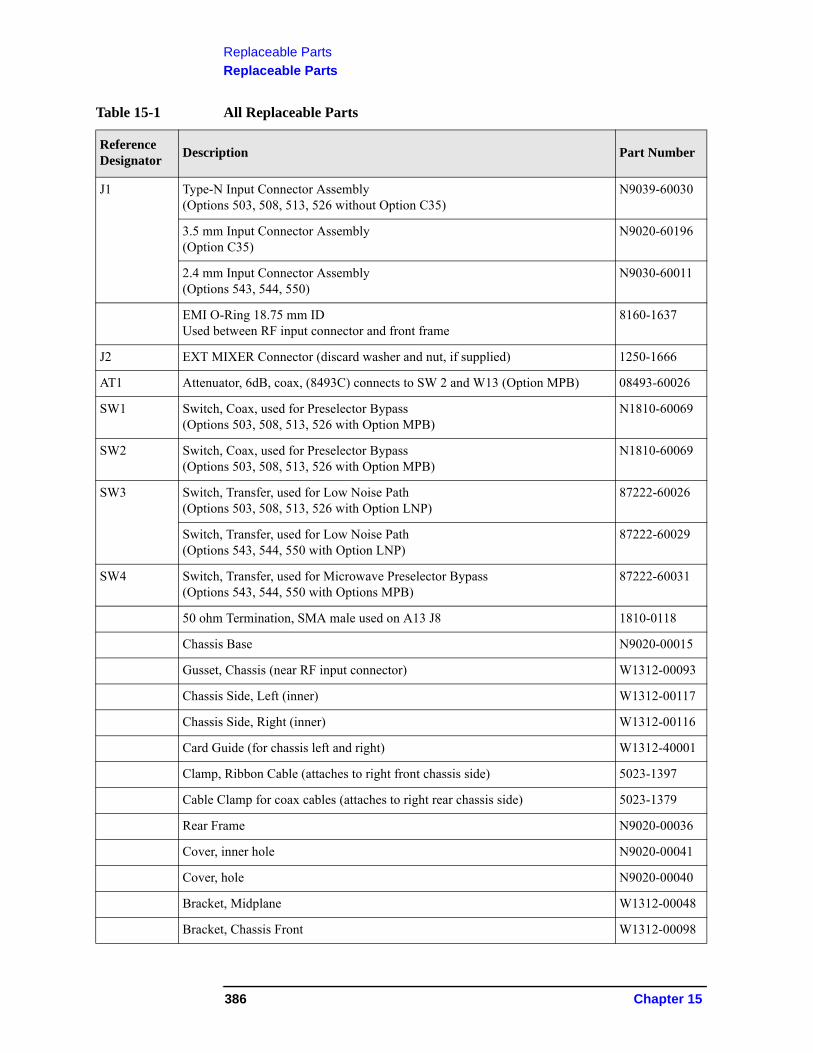
Replaceable Parts
Replaceable Parts
J1 Type-N Input Connector Assembly (Options 503, 508, 513, 526 without Option C35)
N9039-60030
3.5 mm Input Connector Assembly (Option C35)
N9020-60196
2.4 mm Input Connector Assembly (Options 543, 544, 550)
N9030-60011
EMI O-Ring 18.75 mm IDUsed between RF input connector and front frame
8160-1637
J2 EXT MIXER Connector (discard washer and nut, if supplied) 1250-1666
AT1 Attenuator, 6dB, coax, (8493C) connects to SW 2 and W13 (Option MPB) 08493-60026
SW1 Switch, Coax, used for Preselector Bypass (Options 503, 508, 513, 526 with Option MPB)
N1810-60069
SW2 Switch, Coax, used for Preselector Bypass (Options 503, 508, 513, 526 with Option MPB)
N1810-60069
SW3 Switch, Transfer, used for Low Noise Path (Options 503, 508, 513, 526 with Option LNP)
87222-60026
Switch, Transfer, used for Low Noise Path (Options 543, 544, 550 with Option LNP)
87222-60029
SW4 Switch, Transfer, used for Microwave Preselector Bypass(Options 543, 544, 550 with Options MPB)
87222-60031
50 ohm Termination, SMA male used on A13 J8 1810-0118
Chassis Base N9020-00015
Gusset, Chassis (near RF input connector) W1312-00093
Chassis Side, Left (inner) W1312-00117
Chassis Side, Right (inner) W1312-00116
Card Guide (for chassis left and right) W1312-40001
Clamp, Ribbon Cable (attaches to right front chassis side) 5023-1397
Cable Clamp for coax cables (attaches to right rear chassis side) 5023-1379
Rear Frame N9020-00036
Cover, inner hole N9020-00041
Cover, hole N9020-00040
Bracket, Midplane W1312-00048
Bracket, Chassis Front W1312-00098
Table 15-1 All Replaceable Parts
Reference Designator
Description Part Number
386 Chapter 15
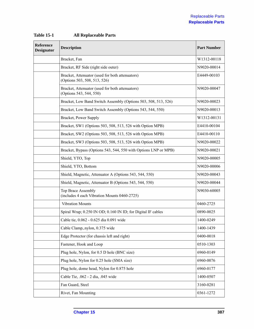
Replaceable Parts
Replaceable Parts
Bracket, Fan W1312-00118
Bracket, RF Side (right side outer) N9020-00014
Bracket, Attenuator (used for both attenuators) (Options 503, 508, 513, 526)
E4449-00103
Bracket, Attenuator (used for both attenuators) (Options 543, 544, 550)
N9020-00047
Bracket, Low Band Switch Assembly (Options 503, 508, 513, 526) N9020-00023
Bracket, Low Band Switch Assembly (Options 543, 544, 550) N9020-00013
Bracket, Power Supply W1312-00131
Bracket, SW1 (Options 503, 508, 513, 526 with Option MPB) E4410-00104
Bracket, SW2 (Options 503, 508, 513, 526 with Option MPB) E4410-00110
Bracket, SW3 (Options 503, 508, 513, 526 with Option MPB) N9020-00022
Bracket, Bypass (Options 543, 544, 550 with Options LNP or MPB) N9020-00021
Shield, YTO, Top N9020-00005
Shield, YTO, Bottom N9020-00006
Shield, Magnetic, Attenuator A (Options 543, 544, 550) N9020-00043
Shield, Magnetic, Attenuator B (Options 543, 544, 550) N9020-00044
Top Brace Assembly(includes 4 each Vibration Mounts 0460-2725)
N9030-60005
Vibration Mounts 0460-2725
Spiral Wrap; 0.250 IN OD; 0.160 IN ID; for Digital IF cables 0890-0025
Cable tie, 0.062 - 0.625 dia 0.091 wide 1400-0249
Cable Clamp,.nylon, 0.375 wide 1400-1439
Edge Protector (for chassis left and right) 0400-0018
Fastener, Hook and Loop 0510-1303
Plug hole, Nylon, for 0.5 D hole (BNC size) 6960-0149
Plug hole, Nylon for 0.25 hole (SMA size) 6960-0076
Plug hole, dome head, Nylon for 0.875 hole 6960-0177
Cable Tie, .062 - 2 dia, .045 wide 1400-0507
Fan Guard, Steel 3160-0281
Rivet, Fan Mounting 0361-1272
Table 15-1 All Replaceable Parts
Reference Designator
Description Part Number
Chapter 15 387
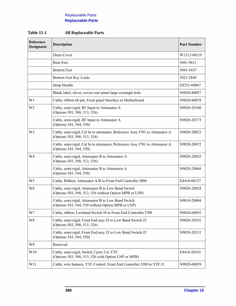
Replaceable Parts
Replaceable Parts
Dress Cover W1312-00119
Rear Feet 5041-9611
Bottom Feet 5041-9167
Bottom Feet Key Locks 5021-2840
Strap Handle E8251-60067
Blank label, silver, covers rear panel large rectangle hole N9020-80057
W1 Cable, ribbon 68 pin, Front panel Interface to Motherboard N9020-60078
W2 Cable, semi-rigid, RF Input to Attenuator A (Options 503, 508, 513, 526)
N9020-20100
Cable, semi-rigid, RF Input to Attenuator A (Options 543, 544, 550)
N9020-20173
W3 Cable, semi-rigid, Cal In to attenuator, Reference Assy J701 to Attenuator A(Options 503, 508, 513, 526)
N9020-20023
Cable, semi-rigid, Cal In to attenuator, Reference Assy J701 to Attenuator A(Options 543, 544, 550)
N9020-20072
W4 Cable, semi-rigid, Attenuator B to Attenuator A (Options 503, 508, 513, 526)
N9020-20025
Cable, semi-rigid, Attenuator B to Attenuator A(Options 543, 544, 550)
N9020-20068
W5 Cable, Ribbon, Attenuator A/B to Front End Controller J800 E4410-60157
W6 Cable, semi-rigid, Attenuator B to Low Band Switch(Options 503, 508, 513, 526 without Option MPB or LNP)
N9020-20024
Cable, semi-rigid, Attenuator B to Low Band Switch(Options 543, 544, 550 without Option MPB or LNP)
N9010-20004
W7 Cable, ribbon, Lowband Switch J4 to Front End Controller J700 N9020-60092
W8 Cable, semi-rigid, Front End assy J2 to Low Band Switch J2(Options 503, 508, 513, 526)
N9020-20101
Cable, semi-rigid, Front End assy J2 to Low Band Switch J2(Options 543, 544, 550)
N9020-20131
W9 Reserved
W10 Cable, semi-rigid, Switch 2 port 2 to YTF (Options 503, 508, 513, 526 with Option LNP or MPB)
E4410-20163
W11 Cable, wire harness, YTF Control, Front End Controller J300 to YTF J1 N9020-60059
Table 15-1 All Replaceable Parts
Reference Designator
Description Part Number
388 Chapter 15
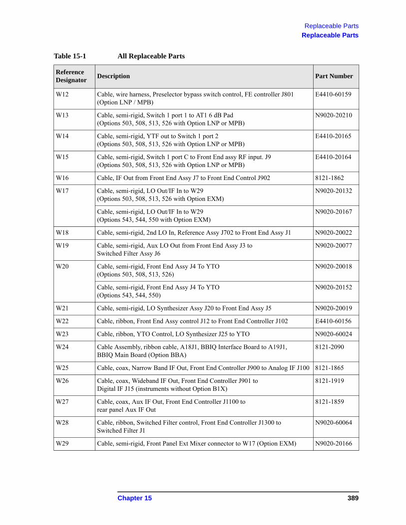
Replaceable Parts
Replaceable Parts
W12 Cable, wire harness, Preselector bypass switch control, FE controller J801 (Option LNP / MPB)
E4410-60159
W13 Cable, semi-rigid, Switch 1 port 1 to AT1 6 dB Pad(Options 503, 508, 513, 526 with Option LNP or MPB)
N9020-20210
W14 Cable, semi-rigid, YTF out to Switch 1 port 2 (Options 503, 508, 513, 526 with Option LNP or MPB)
E4410-20165
W15 Cable, semi-rigid, Switch 1 port C to Front End assy RF input. J9 (Options 503, 508, 513, 526 with Option LNP or MPB)
E4410-20164
W16 Cable, IF Out from Front End Assy J7 to Front End Control J902 8121-1862
W17 Cable, semi-rigid, LO Out/IF In to W29 (Options 503, 508, 513, 526 with Option EXM)
N9020-20132
Cable, semi-rigid, LO Out/IF In to W29 (Options 543, 544, 550 with Option EXM)
N9020-20167
W18 Cable, semi-rigid, 2nd LO In, Reference Assy J702 to Front End Assy J1 N9020-20022
W19 Cable, semi-rigid, Aux LO Out from Front End Assy J3 to Switched Filter Assy J6
N9020-20077
W20 Cable, semi-rigid, Front End Assy J4 To YTO (Options 503, 508, 513, 526)
N9020-20018
Cable, semi-rigid, Front End Assy J4 To YTO (Options 543, 544, 550)
N9020-20152
W21 Cable, semi-rigid, LO Synthesizer Assy J20 to Front End Assy J5 N9020-20019
W22 Cable, ribbon, Front End Assy control J12 to Front End Controller J102 E4410-60156
W23 Cable, ribbon, YTO Control, LO Synthesizer J25 to YTO N9020-60024
W24 Cable Assembly, ribbon cable, A18J1, BBIQ Interface Board to A19J1, BBIQ Main Board (Option BBA)
8121-2090
W25 Cable, coax, Narrow Band IF Out, Front End Controller J900 to Analog IF J100 8121-1865
W26 Cable, coax, Wideband IF Out, Front End Controller J901 to Digital IF J15 (instruments without Option B1X)
8121-1919
W27 Cable, coax, Aux IF Out, Front End Controller J1100 to rear panel Aux IF Out
8121-1859
W28 Cable, ribbon, Switched Filter control, Front End Controller J1300 to Switched Filter J1
N9020-60064
W29 Cable, semi-rigid, Front Panel Ext Mixer connector to W17 (Option EXM) N9020-20166
Table 15-1 All Replaceable Parts
Reference Designator
Description Part Number
Chapter 15 389
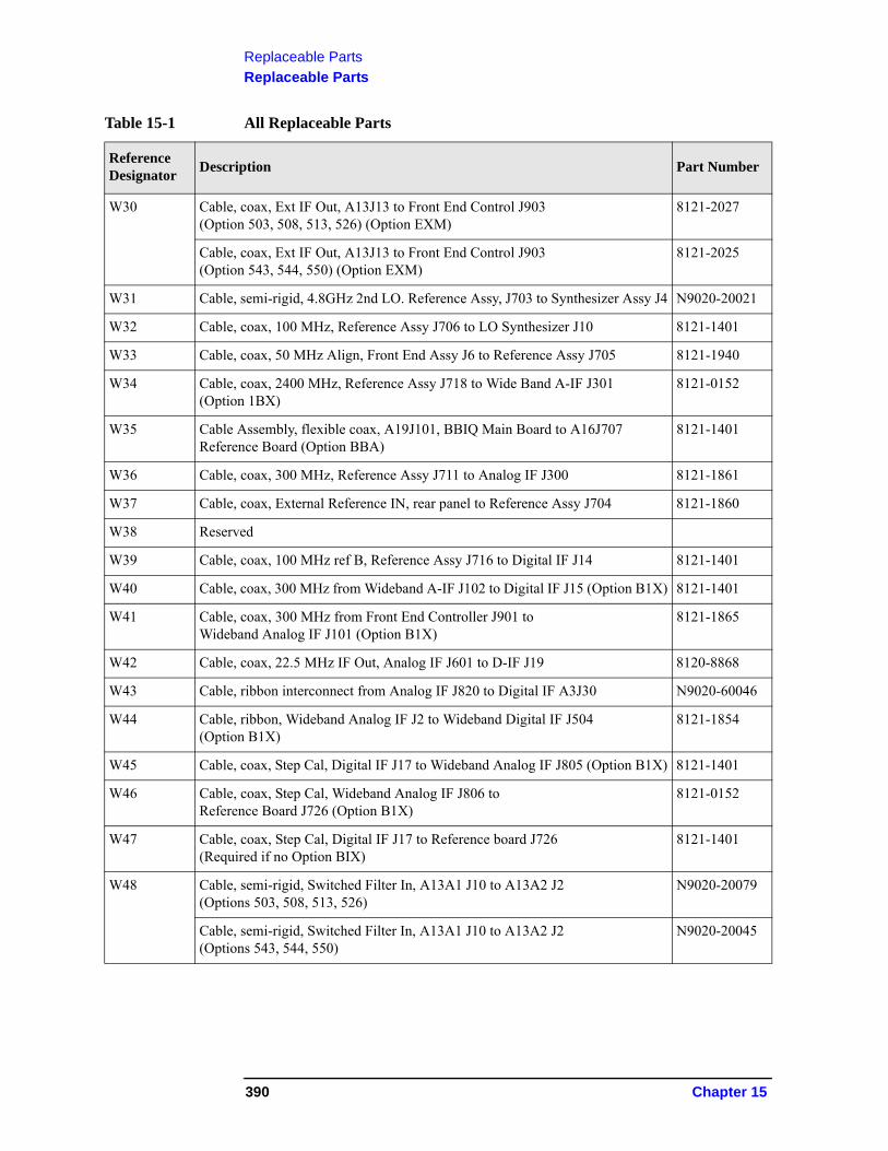
Replaceable Parts
Replaceable Parts
W30 Cable, coax, Ext IF Out, A13J13 to Front End Control J903(Option 503, 508, 513, 526) (Option EXM)
8121-2027
Cable, coax, Ext IF Out, A13J13 to Front End Control J903(Option 543, 544, 550) (Option EXM)
8121-2025
W31 Cable, semi-rigid, 4.8GHz 2nd LO. Reference Assy, J703 to Synthesizer Assy J4 N9020-20021
W32 Cable, coax, 100 MHz, Reference Assy J706 to LO Synthesizer J10 8121-1401
W33 Cable, coax, 50 MHz Align, Front End Assy J6 to Reference Assy J705 8121-1940
W34 Cable, coax, 2400 MHz, Reference Assy J718 to Wide Band A-IF J301 (Option 1BX)
8121-0152
W35 Cable Assembly, flexible coax, A19J101, BBIQ Main Board to A16J707 Reference Board (Option BBA)
8121-1401
W36 Cable, coax, 300 MHz, Reference Assy J711 to Analog IF J300 8121-1861
W37 Cable, coax, External Reference IN, rear panel to Reference Assy J704 8121-1860
W38 Reserved
W39 Cable, coax, 100 MHz ref B, Reference Assy J716 to Digital IF J14 8121-1401
W40 Cable, coax, 300 MHz from Wideband A-IF J102 to Digital IF J15 (Option B1X) 8121-1401
W41 Cable, coax, 300 MHz from Front End Controller J901 to Wideband Analog IF J101 (Option B1X)
8121-1865
W42 Cable, coax, 22.5 MHz IF Out, Analog IF J601 to D-IF J19 8120-8868
W43 Cable, ribbon interconnect from Analog IF J820 to Digital IF A3J30 N9020-60046
W44 Cable, ribbon, Wideband Analog IF J2 to Wideband Digital IF J504 (Option B1X)
8121-1854
W45 Cable, coax, Step Cal, Digital IF J17 to Wideband Analog IF J805 (Option B1X) 8121-1401
W46 Cable, coax, Step Cal, Wideband Analog IF J806 to Reference Board J726 (Option B1X)
8121-0152
W47 Cable, coax, Step Cal, Digital IF J17 to Reference board J726(Required if no Option BIX)
8121-1401
W48 Cable, semi-rigid, Switched Filter In, A13A1 J10 to A13A2 J2(Options 503, 508, 513, 526)
N9020-20079
Cable, semi-rigid, Switched Filter In, A13A1 J10 to A13A2 J2(Options 543, 544, 550)
N9020-20045
Table 15-1 All Replaceable Parts
Reference Designator
Description Part Number
390 Chapter 15
Replaceable Parts
Replaceable Parts
W49 Cable, semi-rigid, Switched Filter Out, A13A2 J5 to A13A1 J11(Options 503, 508, 513, 526)
N9020-20078
Cable, semi-rigid, Switched Filter Out, A13A2 J5 to A13A1 J11(Options 543, 544, 550)
N9020-20110
W50 Reserved
W51 Cable, semi-rigid, Input attenuator B to Switch 3 port 1(Options 503, 508, 513, 526 with Option LNP or MPB)
N9020-20143
Cable, semi-rigid, Input attenuator B to Switch 3 port 1(Options 543, 544, 550 with Option LNP or MPB)
N9020-20171
W52 Cable, semi-rigid, Switch 3 port 4 to A11 Low Band Switch J1 (Options 503, 508, 513, 526 with Option LNP or MPB)
N9020-20146
Cable, semi-rigid, Switch 3 port 4 to A11 Low Band Switch J1 (Options 543, 544, 550 with Option LNP or MPB)
N9020-20125
W53 Cable, semi-rigid, Switch 3 port 2 to Switch 2 Port C (Options 503, 508, 513, 526 with Option LNP or MPB)
N9020-20144
W54 Cable, semi-rigid, Switch 3 port 3 to A11 Low Band Switch J3 (Options 503, 508, 513, 526 with Option LNP or MPB)
N9020-20145
Cable, semi-rigid, Switch 3 port 3 to A11 Low Band Switch J3 (Options 543, 544, 550 with Option LNP or MPB)
N9020-20127
W55 Cable, ribbon, Low Band Switch Bypass Control.Switch 3 to A15 Front End Controller J802(Options 503, 508, 513, 526 with Option LNP or MPB)
N9020-60087
Cable, ribbon, Low Band Switch Bypass Control.Switch 3 to A15 Front End Controller J802(Options 543, 544, 550 with Option LNP or MPB)
N9020-60177
W56 Cable, semi-rigid, Low band Switch assy J3 to YTF input(Options 503, 508, 513, 526 without Option MPB or LNP)
N9020-20123
Cable, semi-rigid, Low band Switch assy J3 to YTF input(Options 543, 544, 550 without Option MPB or LNP)
N9010-20005
W57 Cable, semi-rigid, YTF output to Front End assy J9(Options 503, 508, 513, 526 without Option MPB or LNP)
N9020-20124
Cable, semi-rigid, YTF output to Front End assy J9(Options 543, 544, 550 without Option MPB or LNP)
N9010-20006
W58 Cable, semi-rigid, Delay Line, A13A2 Switched Filter J3 to J4 N9020-20080
W59 Cable, semi-rigid, Switch 3 Port 2 to Switch 4 Port 1(Options 543, 544, 550 with Option LNP or MPB)
N9020-20151
Table 15-1 All Replaceable Parts
Reference Designator
Description Part Number
Chapter 15 391
Replaceable Parts
Replaceable Parts
W60 Cable, semi-rigid, Switch 4 Port 4 to YTF Input(Options 543, 544, 550 with Option LNP or MPB)
N9020-20128
W61 Cable, semi-rigid, YTF Output to Switch 4 Port 3(Options 543, 544, 550 with Option LNP or MPB)
N9020-20129
W62 Cable, semi-rigid, Switch 4 Port 2 to A13A1 Input J9(Options 543, 544, 550 with Option LNP or MPB)
N9020-20130
a. Does not include nameplate, See A1MP3 through A1 MP6 and A1MP20 through A1MP22.b. Does not include A1A1MP20 or A1A1MP21 overlays.
Table 15-1 All Replaceable Parts
Reference Designator
Description Part Number
392 Chapter 15
Ch
apter 15
39
3
Rep
lace
able P
arts
Re
plac
eab
le P
arts
Tool Torque
Torx T-10 9 inch-lbs
Torx T-10 9 inch-lbs
Torx T-10 9 inch-lbs
Torx T-10 9 inch-lbs
Torx T-10 9 inch-lbs
Torx T-10 9 inch-lbs
Torx T-10 9 inch-lbs
Torx T-10 9 inch-lbs
Torx T-10 9 inch-lbs
Torx T-10 9 inch-lbs
Torx T-10 9 inch-lbs
Torx T-10 9 inch-lbs
Torx T-8 5 inch-lbs
Torx T-10 9 inch-lbs
Torx T-10 9 inch-lbs
Table 15-2 Attaching Hardware
Attach To Qty Part Number Type
Analog IF Digital IF 3 0515-0372 M3 X 0.5(8 mm long)
Attenuators Attenuator Bracket 2 per 0515-0372 M3 X 0.5(8 mm long)
Attenuator Bracket Chassis 2 per 0515-0372 M3 X 0.5(8 mm long)
Backlight Inverter Board Inverter Bracket 2 0515-0372 M3 X 0.5(8 mm long)
Backlight Inverter Top Shield Backlight Inverter Bottom Shield 8 0515-0372 M3 X 0.5(8 mm long)
Chassis Bottom Chassis Front & Side Brackets 15 0515-0372 M3 X 0.5(8 mm long)
Chassis Front Bracket Chassis 10 0515-0372 M3 X 0.5(8 mm long)
Chassis Gusset Chassis 3 0515-0372 M3 X 0.5(8 mm long)
Chassis Side (Right Outside)
Chassis 8 0515-0372 M3 X 0.5(8 mm long)
CPU Assembly Chassis 6 0515-0372 M3 X 0.5(8 mm long)
CPU Top Shield CPU Assembly 3 0515-0372 M3 X 0.5(8 mm long)
19 0515-1227 M3 X 0.5(6 mm long)
Display Display Bracket 4 0515-0367 M2.5 X 0.45(8 mm long)
Display Bracket Front Frame 2 0515-0372 M3 X 0.5 (8 mm long)
Disk Drive Disk Drive Tray 4 0515-0372 M3 X 0.5 (8 mm long)
394
Ch
apter 15
Re
place
able
Pa
rts
Re
pla
ceab
le P
arts
Torx T-10 9 inch-lbs
Torx T-10 9 inch-lbs
Torx T-8 6 inch-lbs
n/a n/a
9/16” Nut Driver
21 inch-lbs
n/a n/a
Torx T-10 9 inch-lbs
Torx T-10 9 inch-lbs
Torx T-10 9 inch-lbs
Torx T-10 9 inch-lbs
Torx T-10 9 inch lbs.
Torx T-10 9 inch-lbs
Torx T-10 9 inch-lbs
Torx T-10 9 inch-lbs
Torx T-10 9 inch-lbs
)Torx T-10 9 inch-lbs
Tool Torque
Disk Drive Handle Disk Drive Rear Panel 2 0515-1227 M3 X 0.5 (6 mm long)
Disk Drive Interconnect CPU Assembly 2 0515-0372 M3 X 0.5 (8 mm long)
Disk Drive Rear Panel Disk Drive Tray 4 0515-2219 M2.5 X 0.45(5 mm long)
External Reference BNC Rear Panel 1 2190-0102 Lock Washer
1 0590-2332 Hex Nut
Fan Fan Bracket 4 per 0361-1272 Rivets
Fan Assembly Chassis 7 0515-0372 M3 X 0.5(8 mm long)
Front Frame Assembly Chassis 8 0515-1035 M3 X 0.5(8 mm long)
Front Panel Connector Cover Plate
Front Frame 2 0515-1227 M3 X 0.5 (6 mm long)
Front Panel Daughter Board Front Frame 3 0515-0372 M3 X 0.5(8 mm long)
Front Panel Interface Board Front Frame 13 0515-1521 M3 X 0.5 (5 mm long)
Front Panel Shield Front Frame 4 0515-0372 M3 X 0.5(8 mm long)
LO Synthesizer Assembly Chassis 2 0515-1035 M3 X 0.5(8 mm long)
Low Band Switch Assy. Low Band Switch Bracket 4 0515-0372 M3 X 0.5(8 mm long)
Low Band Switch Bracket. Chassis 2 0515-0372 M3 X 0.5(8 mm long)
Midplane Assembly Midplane Bracket 6 0515-0375 M3 X 0.5(16 mm long
Table 15-2 Attaching Hardware
Attach To Qty Part Number Type
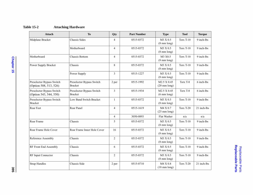
Ch
apter 15
39
5
Rep
lace
able P
arts
Re
plac
eab
le P
arts
Torx T-10 9 inch-lbs
Torx T-10 9 inch-lbs
Torx T-10 9 inch-lbs
Torx T-10 9 inch-lbs
Torx T-10 9 inch-lbs
Torx T-8 6 inch-lbs
Torx T-8 6 inch-lbs
Torx T-10 9 inch-lbs
Torx T-20 21 inch-lbs
n/a n/a
Torx T-10 9 inch-lbs
Torx T-10 9 inch-lbs
Torx T-10 9 inch-lbs
Torx T-10 9 inch-lbs
Torx T-10 9 inch-lbs
Torx T-20 21 inch-lbs
Tool Torque
Midplane Bracket Chassis Sides 4 0515-0372 M3 X 0.5(8 mm long)
Motherboard 4 0515-0372 M3 X 0.5(8 mm long)
Motherboard Chassis Bottom 4 0515-0372 M3 X0.5(8 mm long)
Power Supply Bracket Chassis 8 0515-0372 M3 X 0.5(8 mm long)
Power Supply 3 0515-1227 M3 X 0.5(8 mm long)
Preselector Bypass Switch(Option 508, 513, 526)
Preselector Bypass Switch Bracket
2 per 0515-1992 M2.5 X 0.45(20 mm long)
Preselector Bypass Switch(Option 543, 544, 550)
Preselector Bypass Switch Bracket
3 0515-1934 M2.5 X 0.45(6 mm long)
Preselector Bypass Switch Bracket
Low Band Switch Bracket 1 0515-0372 M3 X 0.5(8 mm long)
Rear Feet Rear Panel 4 0515-1619 M4 X 0.7(25 mm long)
4 3050-0893 Flat Washer
Rear Frame Chassis 5 0515-0372 M3 X 0.5(8 mm long)
Rear Frame Hole Cover Rear Frame Inner Hole Cover 16 0515-0372 M3 X 0.5(8 mm long)
Reference Assembly Chassis 2 0515-0372 M3 X 0.5(8 mm long)
RF Front End Assembly Chassis 6 0515-0372 M3 X 0.5(8 mm long)
RF Input Connector Chassis 2 0515-0372 M3 X 0.5(8 mm long)
Strap Handles Chassis Side 2 per 0515-0710 M4 X 0.8(18 mm long)
Table 15-2 Attaching Hardware
Attach To Qty Part Number Type
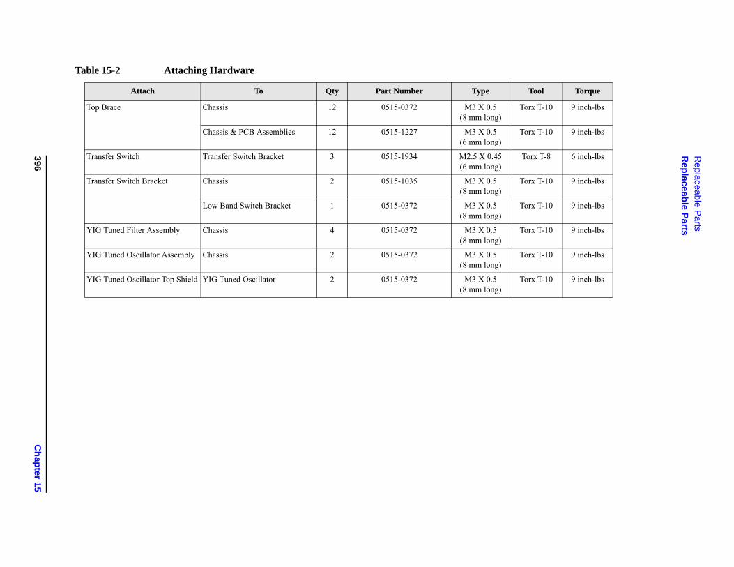
396
Ch
apter 15
Re
place
able
Pa
rts
Re
pla
ceab
le P
arts
Torx T-10 9 inch-lbs
Torx T-10 9 inch-lbs
Torx T-8 6 inch-lbs
Torx T-10 9 inch-lbs
Torx T-10 9 inch-lbs
Torx T-10 9 inch-lbs
Torx T-10 9 inch-lbs
Torx T-10 9 inch-lbs
Tool Torque
Top Brace Chassis 12 0515-0372 M3 X 0.5(8 mm long)
Chassis & PCB Assemblies 12 0515-1227 M3 X 0.5(6 mm long)
Transfer Switch Transfer Switch Bracket 3 0515-1934 M2.5 X 0.45(6 mm long)
Transfer Switch Bracket Chassis 2 0515-1035 M3 X 0.5(8 mm long)
Low Band Switch Bracket 1 0515-0372 M3 X 0.5(8 mm long)
YIG Tuned Filter Assembly Chassis 4 0515-0372 M3 X 0.5(8 mm long)
YIG Tuned Oscillator Assembly Chassis 2 0515-0372 M3 X 0.5(8 mm long)
YIG Tuned Oscillator Top Shield YIG Tuned Oscillator 2 0515-0372 M3 X 0.5(8 mm long)
Table 15-2 Attaching Hardware
Attach To Qty Part Number Type
Replaceable Parts
Hardware
Hardware
Figure 15-1 Major Assemblies
Item Description Agilent Part Number
1 A2 Analog IF AssemblyA3 Digital IF Assembly
N9020-60254N9020-60016
2 A4 CPU Board (without A5 drive or drive tray parts, includes battery)
Serial Prefix Number ≥ MY/SG5136 and US5135
Serial Prefix Number < MY/SG5136 and US5135
N9020-60135
N9020-60081
3 A6 Power Supply 0950-4934
4 A7 Midplane Assembly W1312-63095
5 A16 Reference Assembly (includes associated shields) N9020-60188
6 A25 Wideband Analog IF (Option B1X) N9020-60044
7 A26 Wideband Digital IF (Option B1X) N9020-60047
8 A19 BBIQ Main Board (Option BBA) N9020-65093
9 A14 Synthesizer Assembly N9020-60008
10 A15 Front End Controller N9020-60172
Chapter 15 397
Replaceable Parts
Hardware
Figure 15-2 External Hardware
Item Description Agilent Part Number
1, 2 Strap Handle (includes screws) E8251-60067
3 Screw M4 X 0.7 (25 mm long) 0515-1619
4 Rear Feet 5041-9611
5 Dress Cover W1312-00119
6 Bottom Feet 5041-9167
398 Chapter 15
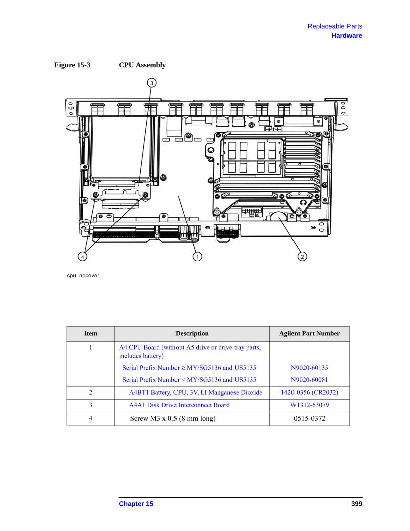
Replaceable Parts
Hardware
Figure 15-3 CPU Assembly
Item Description Agilent Part Number
1 A4 CPU Board (without A5 drive or drive tray parts, includes battery)
Serial Prefix Number ≥ MY/SG5136 and US5135
Serial Prefix Number < MY/SG5136 and US5135
N9020-60135
N9020-60081
2 A4BT1 Battery, CPU, 3V, LI Manganese Dioxide 1420-0356 (CR2032)
3 A4A1 Disk Drive Interconnect Board W1312-63079
4 Screw M3 x 0.5 (8 mm long) 0515-0372
Chapter 15 399
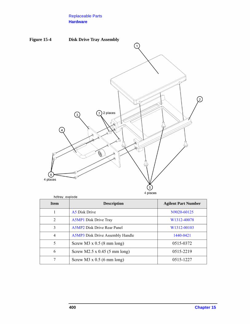
Replaceable Parts
Hardware
Figure 15-4 Disk Drive Tray Assembly
Item Description Agilent Part Number
1 A5 Disk Drive N9020-60125
2 A5MP1 Disk Drive Tray W1312-40078
3 A5MP2 Disk Drive Rear Panel W1312-00103
4 A5MP3 Disk Drive Assembly Handle 1440-0421
5 Screw M3 x 0.5 (8 mm long) 0515-0372
6 Screw M2.5 x 0.45 (5 mm long) 0515-2219
7 Screw M3 x 0.5 (6 mm long) 0515-1227
400 Chapter 15
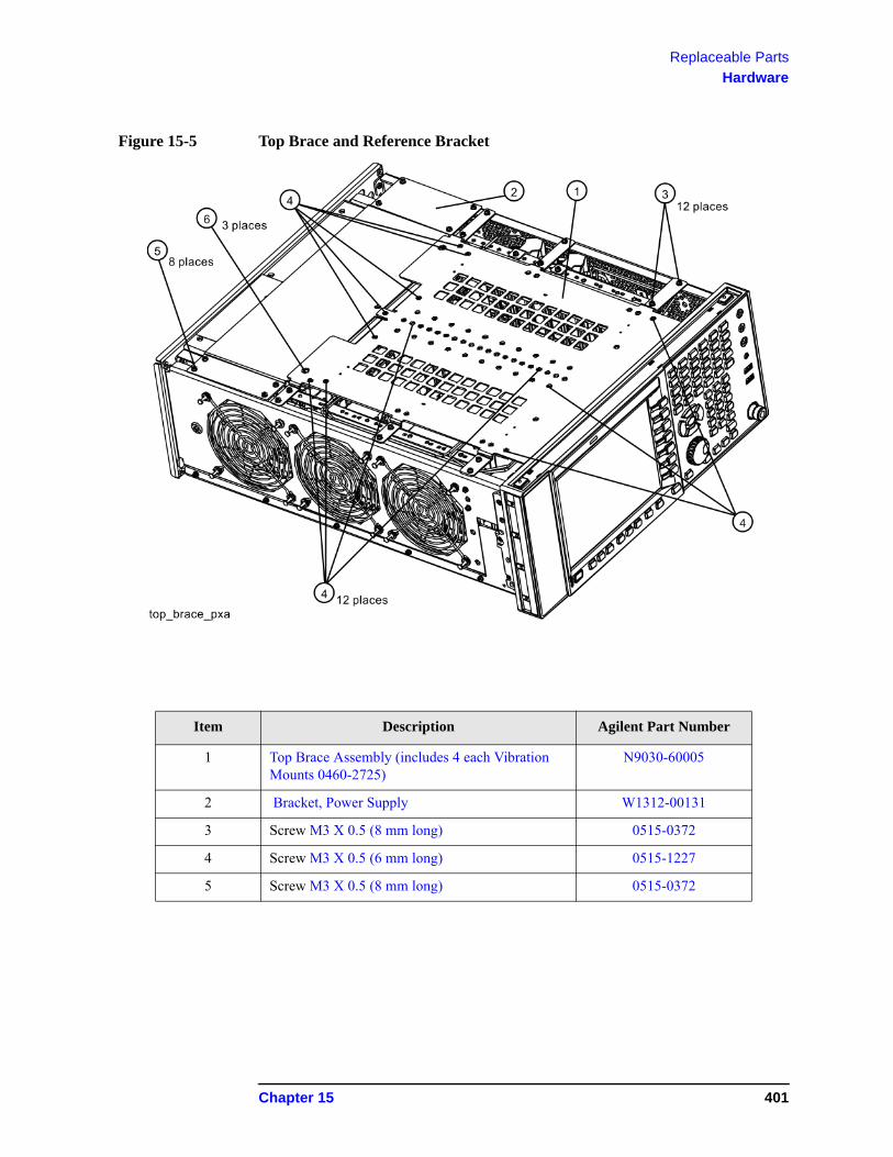
Replaceable Parts
Hardware
Figure 15-5 Top Brace and Reference Bracket
Item Description Agilent Part Number
1 Top Brace Assembly (includes 4 each Vibration Mounts 0460-2725)
N9030-60005
2 Bracket, Power Supply W1312-00131
3 Screw M3 X 0.5 (8 mm long) 0515-0372
4 Screw M3 X 0.5 (6 mm long) 0515-1227
5 Screw M3 X 0.5 (8 mm long) 0515-0372
Chapter 15 401
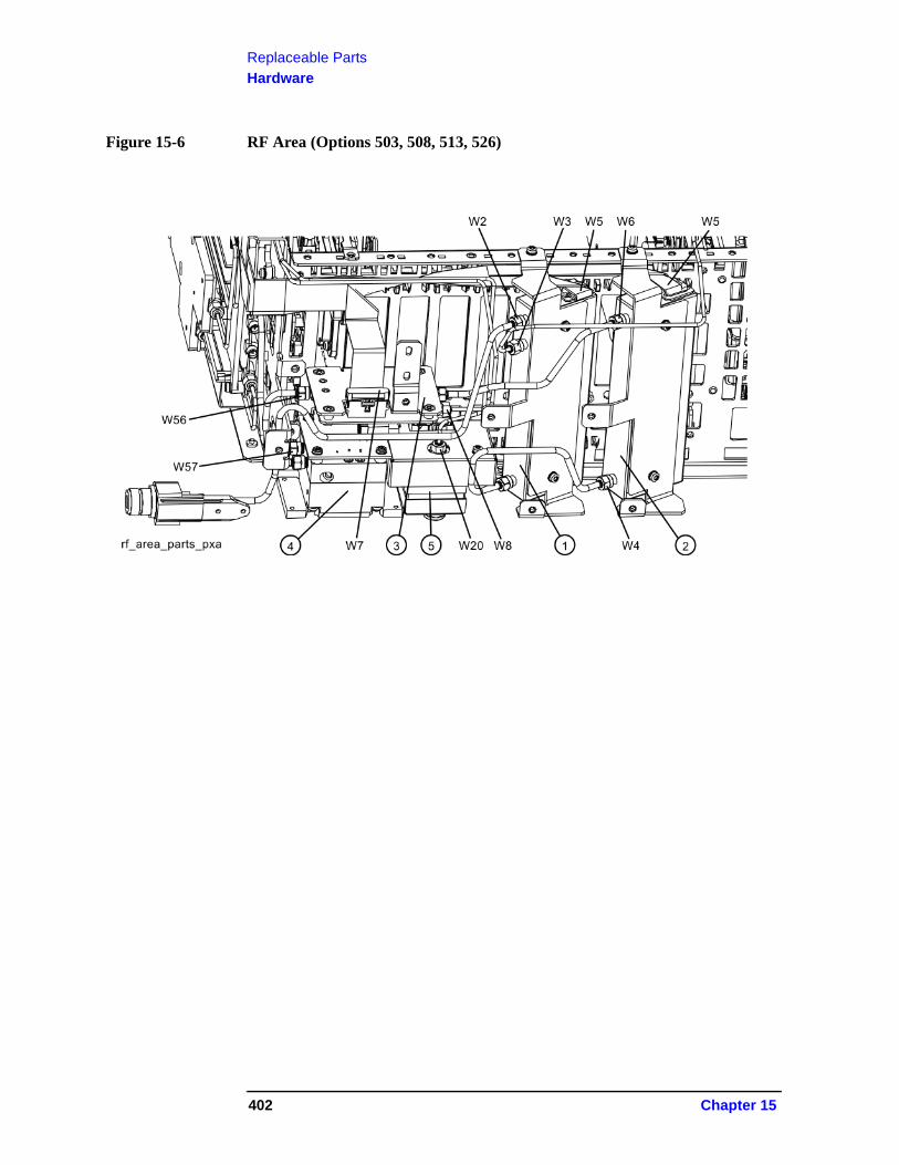
Replaceable Parts
Hardware
Figure 15-6 RF Area (Options 503, 508, 513, 526)
402 Chapter 15
Replaceable Parts
Hardware
Item Description Agilent Part Number
1 A9 RF Attenuator A (0-4 dB) (Options 503, 508, 513, 526) 33360-60008
2 A10 RF Attenuator B (0-66 dB) (Options 503, 508, 513, 526) 33321-60083
3 A11 Low Band Switch Assembly (Options 503, 508, 513, 526) E4410-60121
4 A12 YTF Preselector (Options 503, 508, 513, 526) 5087-7828
5 A20 YTO Assembly N9020-60009
W2 Cable, semi-rigid, RF Input to Attenuator A (Options 503, 508, 513, 526)
N9020-20100
W3 Cable, semi-rigid, Cal In to attenuator, Reference Assy J701 to Attenuator A (Options 503, 508, 513, 526)
N9020-20023
W4 Cable, semi-rigid, Attenuator B to Attenuator A (Options 503, 508, 513, 526)
N9020-20025
W5 Cable, Ribbon, Attenuator A/B to Front End Controller J800 E4410-60157
W6 Cable, semi-rigid, Attenuator B to Low Band Switch (Options 503, 508, 513, 526 without Option MPB or LNP)
N9020-20024
W7 Cable, ribbon, Lowband Switch J4 to Front End Controller J700 N9020-60092
W8 Cable, semi-rigid, Front End assy J2 to Low Band Switch J2 (Options 503, 508, 513, 526)
N9020-20101
W20 Cable, semi-rigid, Front End Assy J4 To YTO (Options 503, 508, 513, 526)
N9020-20018
W56 Cable, semi-rigid, Low band Switch assy J3 to YTF input (Options 503, 508, 513, 526 without Option MPB or LNP)
N9020-20123
W57 Cable, semi-rigid, YTF output to Front End assy J9 (Options 503, 508, 513, 526 without Option MPB or LNP)
N9020-20124
Chapter 15 403
Replaceable Parts
Hardware
Figure 15-7 RF Area (Options 543, 544, 550)
404 Chapter 15
Replaceable Parts
Hardware
Item Description Agilent Part Number
1 A9 RF Attenuator A (0-10 dB) (Options 543, 544, 550) 33326-60012
2 A10 RF Attenuator B (0-60 dB) (Options 543, 544, 550) 33325-60018
3 A11 Low Band Switch Assembly (Options 543, 544, 550) N9020-60051
4 A12 YTF Preselector (Options 543, 544, 550) 5087-7326
5 A20 YTO Assembly N9020-60009
J1 2.4 mm Input Connector Assembly (Options 543, 544, 550) N9030-60011
W2 Cable, semi-rigid, RF Input to Attenuator A (Options 543, 544, 550)
N9020-20173
W3 Cable, semi-rigid, Cal In to attenuator, Reference Assy J701 to Attenuator A (Options 543, 544, 550)
N9020-20072
W4 Cable, semi-rigid, Attenuator B to Attenuator A (Options 543, 544, 550)
N9020-20068
W5 Cable, Ribbon, Attenuator A/B to Front End Controller J800 E4410-60157
W6 Cable, semi-rigid, Attenuator B to Low Band Switch (Options 543, 544, 550 without Option MPB or LNP)
N9010-20004
W7 Cable, ribbon, Lowband Switch J4 to Front End Controller J700 N9020-60092
W8 Cable, semi-rigid, Front End assy J2 to Low Band Switch J2 (Options 543, 544, 550)
N9020-20131
W20 Cable, semi-rigid, Front End Assy J4 To YTO (Options 503, 508, 513, 526)
N9020-20152
W56 Cable, semi-rigid, Low band Switch assy J3 to YTF input (Options 543, 544, 550 without Option MPB or LNP)
N9010-20005
W57 Cable, semi-rigid, YTF output to Front End assy J9 (Options 543, 544, 550 without Option MPB or LNP)
N9010-20006
Chapter 15 405
Replaceable Parts
Hardware
Figure 15-8 Front End Parts (Options 503, 508, 513, 526)
Item Description Agilent Part Number
A13 A13 Front End Assembly (Options 503, 508, 513, 526) Serial Prefix Numbers ≥ MY/SG/US5235
N9020-60143
J1 Type-N Input Connector Assembly (Options 503, 508, 513, 526 without Option C35)
N9039-60030
W16 Cable, IF Out from Front End Assy J7 to Front End Control J902 8121-1862
W18 Cable, semi-rigid, 2nd LO In, Reference Assy J702 to Front End Assy J1 N9020-20022
W19 Cable, semi-rigid, Aux LO Out from Front End Assy J3 to Switched Filter Assy J6
N9020-20077
W20 Cable, semi-rigid, Front End Assy J4 To YTO (Options 503, 508, 513, 526) N9020-20018
W21 Cable, semi-rigid, LO Synthesizer Assy J20 to Front End Assy J5 N9020-20019
W22 Cable, ribbon, Front End Assy control J12 to Front End Controller J102 E4410-60156
W33 Cable, coax, 50 MHz Align, Front End Assy J6 to Reference Assy J705 8121-1940
W48 Cable, semi-rigid, Switched Filter In, A13A1 J10 to A13A2 J2 (Options 503, 508, 513, 526)
N9020-20079
W49 Cable, semi-rigid, Switched Filter Out, A13A2 J5 to A13A1 J11 (Options 503, 508, 513, 526)
N9020-20078
406 Chapter 15
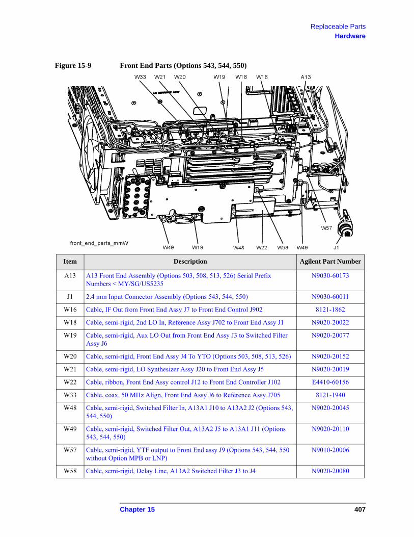
Replaceable Parts
Hardware
Figure 15-9 Front End Parts (Options 543, 544, 550)
Item Description Agilent Part Number
A13 A13 Front End Assembly (Options 503, 508, 513, 526) Serial Prefix Numbers < MY/SG/US5235
N9030-60173
J1 2.4 mm Input Connector Assembly (Options 543, 544, 550) N9030-60011
W16 Cable, IF Out from Front End Assy J7 to Front End Control J902 8121-1862
W18 Cable, semi-rigid, 2nd LO In, Reference Assy J702 to Front End Assy J1 N9020-20022
W19 Cable, semi-rigid, Aux LO Out from Front End Assy J3 to Switched Filter Assy J6
N9020-20077
W20 Cable, semi-rigid, Front End Assy J4 To YTO (Options 503, 508, 513, 526) N9020-20152
W21 Cable, semi-rigid, LO Synthesizer Assy J20 to Front End Assy J5 N9020-20019
W22 Cable, ribbon, Front End Assy control J12 to Front End Controller J102 E4410-60156
W33 Cable, coax, 50 MHz Align, Front End Assy J6 to Reference Assy J705 8121-1940
W48 Cable, semi-rigid, Switched Filter In, A13A1 J10 to A13A2 J2 (Options 543, 544, 550)
N9020-20045
W49 Cable, semi-rigid, Switched Filter Out, A13A2 J5 to A13A1 J11 (Options 543, 544, 550)
N9020-20110
W57 Cable, semi-rigid, YTF output to Front End assy J9 (Options 543, 544, 550 without Option MPB or LNP)
N9010-20006
W58 Cable, semi-rigid, Delay Line, A13A2 Switched Filter J3 to J4 N9020-20080
Chapter 15 407
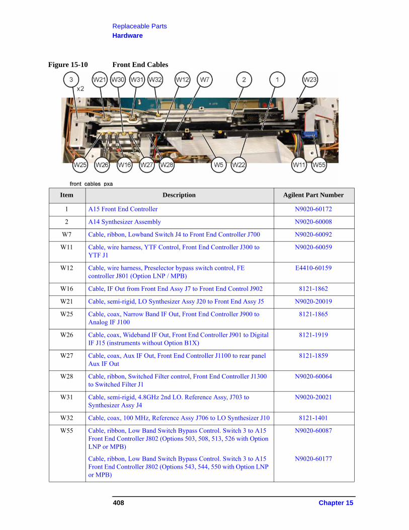
Replaceable Parts
Hardware
Figure 15-10 Front End Cables
Item Description Agilent Part Number
1 A15 Front End Controller N9020-60172
2 A14 Synthesizer Assembly N9020-60008
W7 Cable, ribbon, Lowband Switch J4 to Front End Controller J700 N9020-60092
W11 Cable, wire harness, YTF Control, Front End Controller J300 to YTF J1
N9020-60059
W12 Cable, wire harness, Preselector bypass switch control, FE controller J801 (Option LNP / MPB)
E4410-60159
W16 Cable, IF Out from Front End Assy J7 to Front End Control J902 8121-1862
W21 Cable, semi-rigid, LO Synthesizer Assy J20 to Front End Assy J5 N9020-20019
W25 Cable, coax, Narrow Band IF Out, Front End Controller J900 to Analog IF J100
8121-1865
W26 Cable, coax, Wideband IF Out, Front End Controller J901 to Digital IF J15 (instruments without Option B1X)
8121-1919
W27 Cable, coax, Aux IF Out, Front End Controller J1100 to rear panel Aux IF Out
8121-1859
W28 Cable, ribbon, Switched Filter control, Front End Controller J1300 to Switched Filter J1
N9020-60064
W31 Cable, semi-rigid, 4.8GHz 2nd LO. Reference Assy, J703 to Synthesizer Assy J4
N9020-20021
W32 Cable, coax, 100 MHz, Reference Assy J706 to LO Synthesizer J10 8121-1401
W55 Cable, ribbon, Low Band Switch Bypass Control. Switch 3 to A15 Front End Controller J802 (Options 503, 508, 513, 526 with Option LNP or MPB)
Cable, ribbon, Low Band Switch Bypass Control. Switch 3 to A15 Front End Controller J802 (Options 543, 544, 550 with Option LNP or MPB)
N9020-60087
N9020-60177
408 Chapter 15
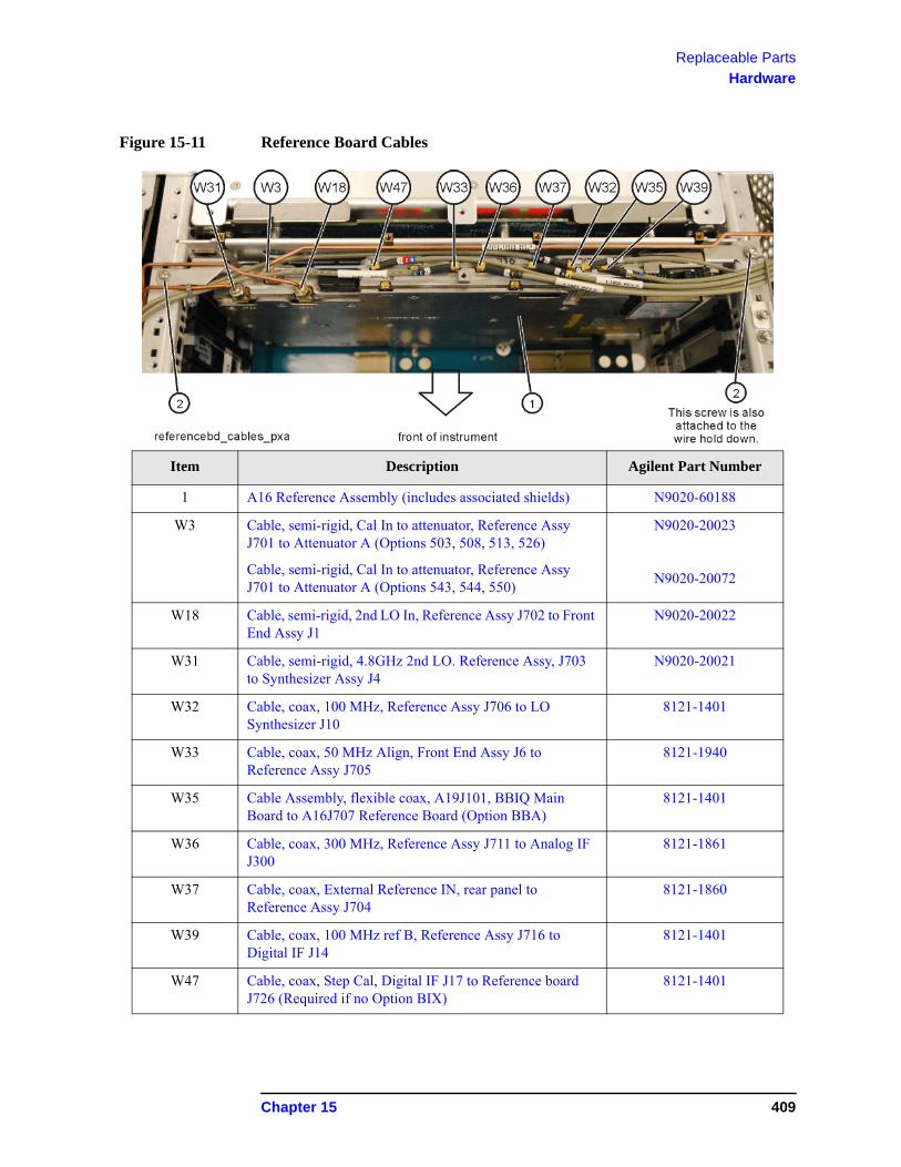
Replaceable Parts
Hardware
Figure 15-11 Reference Board Cables
Item Description Agilent Part Number
1 A16 Reference Assembly (includes associated shields) N9020-60188
W3 Cable, semi-rigid, Cal In to attenuator, Reference Assy J701 to Attenuator A (Options 503, 508, 513, 526)
Cable, semi-rigid, Cal In to attenuator, Reference Assy J701 to Attenuator A (Options 543, 544, 550)
N9020-20023
N9020-20072
W18 Cable, semi-rigid, 2nd LO In, Reference Assy J702 to Front End Assy J1
N9020-20022
W31 Cable, semi-rigid, 4.8GHz 2nd LO. Reference Assy, J703 to Synthesizer Assy J4
N9020-20021
W32 Cable, coax, 100 MHz, Reference Assy J706 to LO Synthesizer J10
8121-1401
W33 Cable, coax, 50 MHz Align, Front End Assy J6 to Reference Assy J705
8121-1940
W35 Cable Assembly, flexible coax, A19J101, BBIQ Main Board to A16J707 Reference Board (Option BBA)
8121-1401
W36 Cable, coax, 300 MHz, Reference Assy J711 to Analog IF J300
8121-1861
W37 Cable, coax, External Reference IN, rear panel to Reference Assy J704
8121-1860
W39 Cable, coax, 100 MHz ref B, Reference Assy J716 to Digital IF J14
8121-1401
W47 Cable, coax, Step Cal, Digital IF J17 to Reference board J726 (Required if no Option BIX)
8121-1401
Chapter 15 409
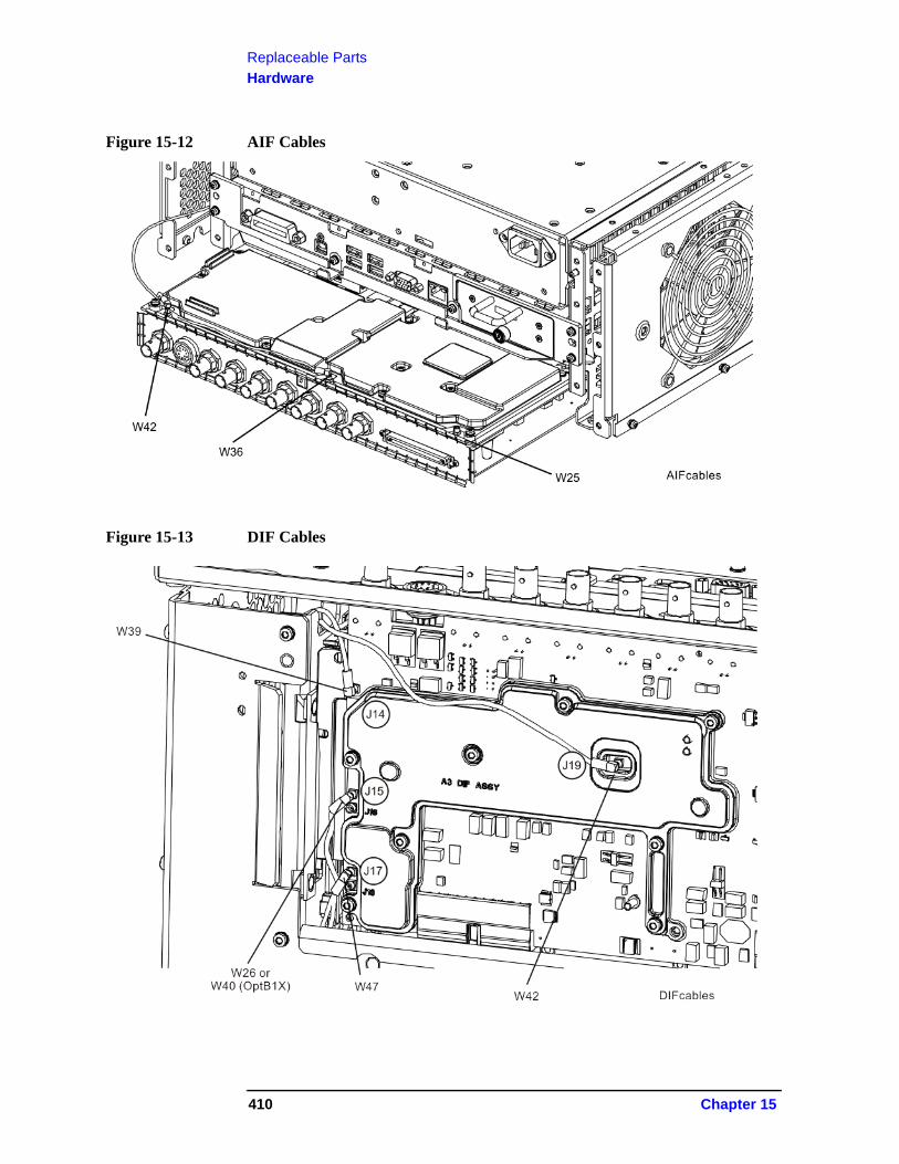
Replaceable Parts
Hardware
Figure 15-12 AIF Cables
Figure 15-13 DIF Cables
410 Chapter 15
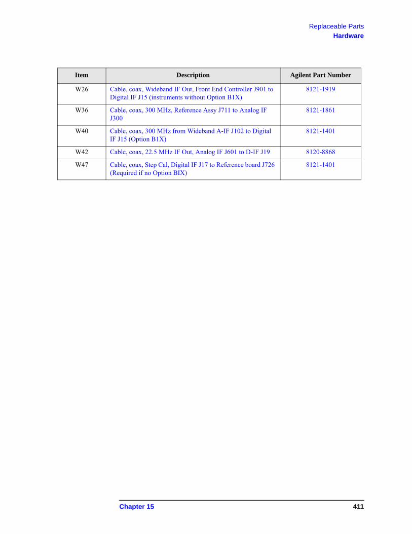
Replaceable Parts
Hardware
Item Description Agilent Part Number
W26 Cable, coax, Wideband IF Out, Front End Controller J901 to Digital IF J15 (instruments without Option B1X)
8121-1919
W36 Cable, coax, 300 MHz, Reference Assy J711 to Analog IF J300
8121-1861
W40 Cable, coax, 300 MHz from Wideband A-IF J102 to Digital IF J15 (Option B1X)
8121-1401
W42 Cable, coax, 22.5 MHz IF Out, Analog IF J601 to D-IF J19 8120-8868
W47 Cable, coax, Step Cal, Digital IF J17 to Reference board J726 (Required if no Option BIX)
8121-1401
Chapter 15 411
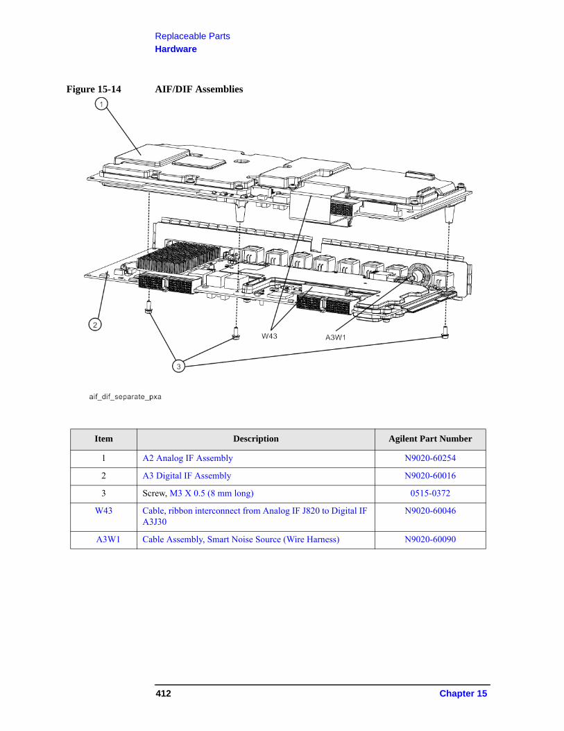
Replaceable Parts
Hardware
Figure 15-14 AIF/DIF Assemblies
Item Description Agilent Part Number
1 A2 Analog IF Assembly N9020-60254
2 A3 Digital IF Assembly N9020-60016
3 Screw, M3 X 0.5 (8 mm long) 0515-0372
W43 Cable, ribbon interconnect from Analog IF J820 to Digital IF A3J30
N9020-60046
A3W1 Cable Assembly, Smart Noise Source (Wire Harness) N9020-60090
412 Chapter 15
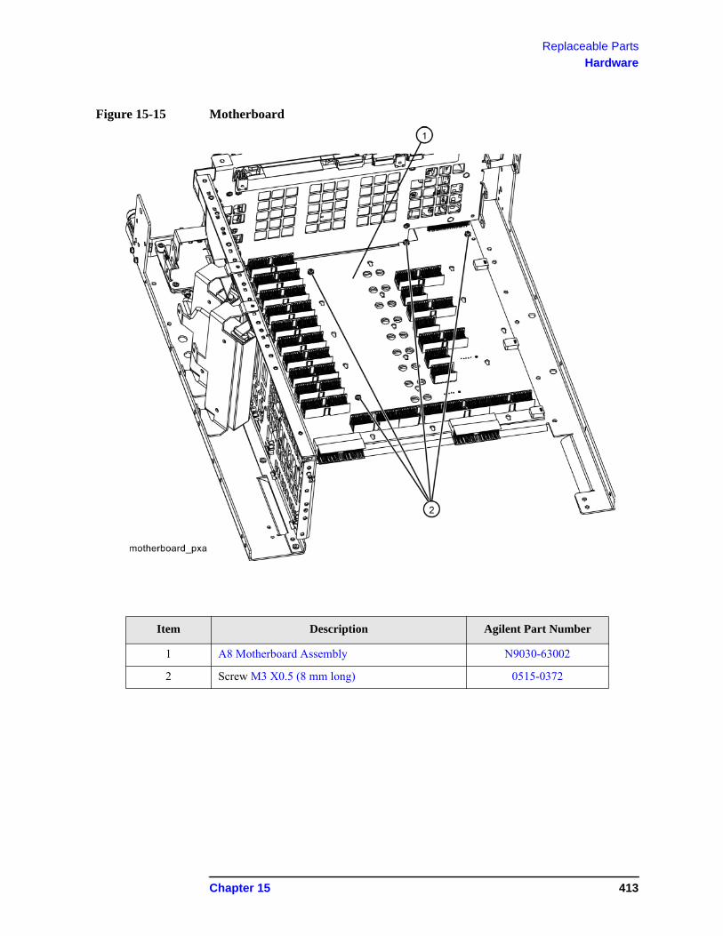
Replaceable Parts
Hardware
Figure 15-15 Motherboard
Item Description Agilent Part Number
1 A8 Motherboard Assembly N9030-63002
2 Screw M3 X0.5 (8 mm long) 0515-0372
Chapter 15 413
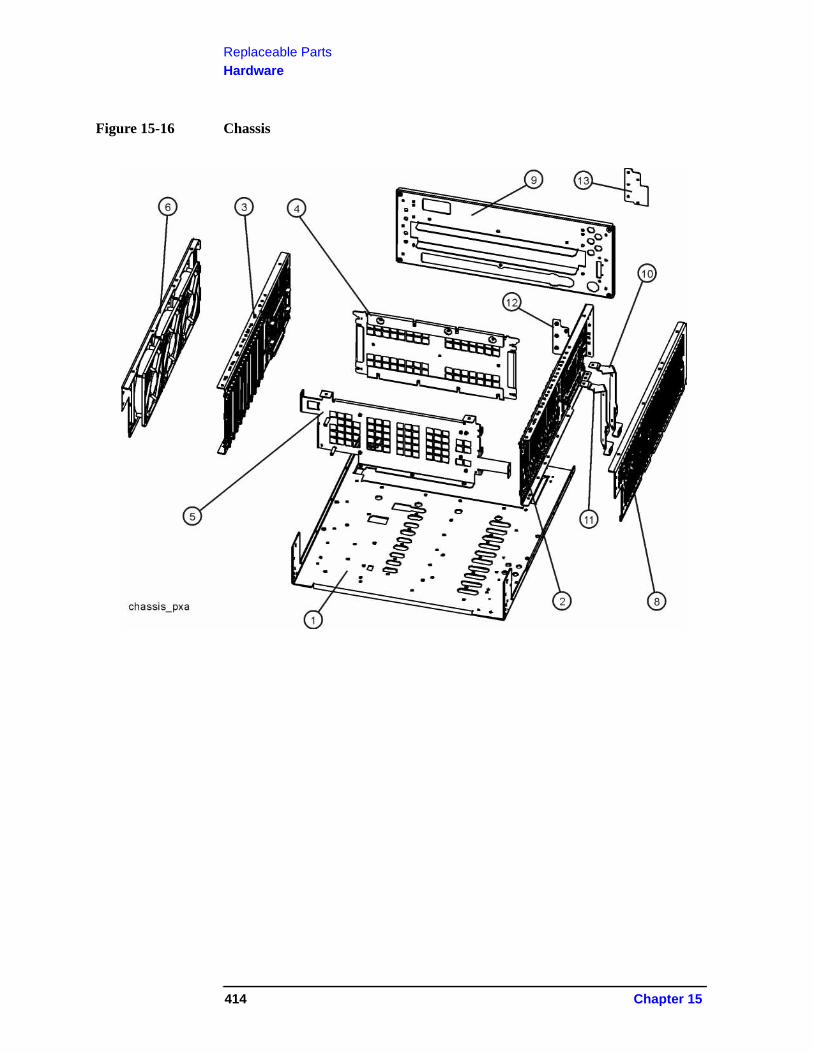
Replaceable Parts
Hardware
Figure 15-16 Chassis
414 Chapter 15
Replaceable Parts
Hardware
Item Description Agilent Part Number
1 Chassis Base N9020-00015
2 Chassis Side, Right (inner) W1312-00116
3 Chassis Side, Left (inner) W1312-00117
4 Bracket, Midplane W1312-00048
5 Bracket, Chassis Front W1312-00098
6 Bracket, Fan W1312-00118
8 Bracket, RF Side (right side outer) N9020-00014
9 Rear Frame N9020-00036
10 + 11 Bracket, Attenuator (used for both attenuators) (Options 503, 508, 513, 526)
Bracket, Attenuator (used for both attenuators) (Options 543, 544, 550)
E4449-00103
N9020-00047
12 Cover, inner hole N9020-00041
13 Cover, hole N9020-00040
Chapter 15 415
Replaceable Parts
Hardware
Figure 15-17 Fan Hardware
Item Description Agilent Part Number
1 B1, B2, B3 Fan 3160-4199
2 Fan Guard, Steel 3160-0281
3 Rivet, Fan Mounting 0361-1272
416 Chapter 15
Replaceable Parts
Hardware
Figure 15-18 Input Connector
Item Description Agilent Part Number
1 Screw M3 X 0.5 (8 mm long) 0515-0372
2 J1 Type-N Input Connector Assembly (Options 503, 508, 513, 526 without Option C35)
J1 3.5 mm Input Connector Assembly (Option C35)
J1 2.4 mm Input Connector Assembly (Options 543, 544, 550)
N9039-60030
N9020-60196
N9030-60011
W2 Cable, semi-rigid, RF Input to Attenuator A (Options 503, 508, 513, 526)
Cable, semi-rigid, RF Input to Attenuator A (Options 543, 544, 550)
N9020-20100
N9020-20173
3 Gusset, Chassis (near RF input connector) W1312-00093
Chapter 15 417
Replaceable Parts
Hardware
Figure 15-19 Front Frame Parts - LCD
Item Description Agilent Part Number
17 A1A5 Front Panel Daughter Board N9020-63193
20 A1MP14 Display Bracket W1312-00115
21 A1MP10-13 Cable Clamp (Front Panel Cables) 1400-1439
22 A1MP18 and A1MP19 Shield, Front Panel N9020-00051
24 A1W2 Cable Assembly, Front Panel Interface Board to Inverter Board
W1312-60113
28 A1MP16 Inverter Shield Top N9020-00010
29 Screw M3 X 0.5 (8 mm long) 0515-0372
32 Screw M3 X 0.5 (8 mm long) 0515-0372
33 A1W2 Grommet 0400-0333
418 Chapter 15
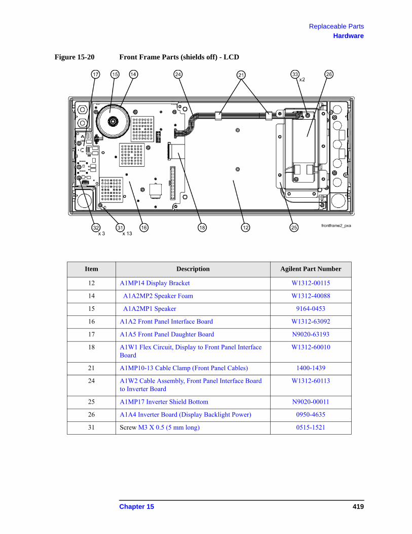
Replaceable Parts
Hardware
Figure 15-20 Front Frame Parts (shields off) - LCD
Item Description Agilent Part Number
12 A1MP14 Display Bracket W1312-00115
14 A1A2MP2 Speaker Foam W1312-40088
15 A1A2MP1 Speaker 9164-0453
16 A1A2 Front Panel Interface Board W1312-63092
17 A1A5 Front Panel Daughter Board N9020-63193
18 A1W1 Flex Circuit, Display to Front Panel Interface Board
W1312-60010
21 A1MP10-13 Cable Clamp (Front Panel Cables) 1400-1439
24 A1W2 Cable Assembly, Front Panel Interface Board to Inverter Board
W1312-60113
25 A1MP17 Inverter Shield Bottom N9020-00011
26 A1A4 Inverter Board (Display Backlight Power) 0950-4635
31 Screw M3 X 0.5 (5 mm long) 0515-1521
Chapter 15 419
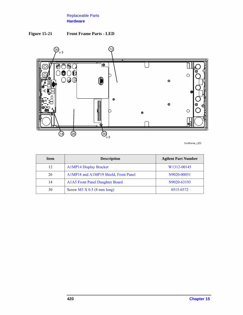
Replaceable Parts
Hardware
Figure 15-21 Front Frame Parts - LED
Item Description Agilent Part Number
12 A1MP14 Display Bracket W1312-00145
26 A1MP18 and A1MP19 Shield, Front Panel N9020-00051
14 A1A5 Front Panel Daughter Board N9020-63193
30 Screw M3 X 0.5 (8 mm long) 0515-0372
420 Chapter 15
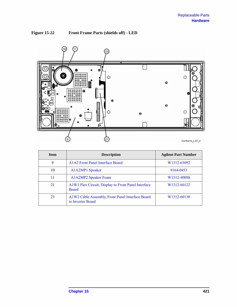
Replaceable Parts
Hardware
Figure 15-22 Front Frame Parts (shields off) - LED
Item Description Agilent Part Number
9 A1A2 Front Panel Interface Board W1312-63092
10 A1A2MP1 Speaker 9164-0453
11 A1A2MP2 Speaker Foam W1312-40088
21 A1W1 Flex Circuit, Display to Front Panel Interface Board
W1312-60122
23 A1W2 Cable Assembly, Front Panel Interface Board to Inverter Board
W1312-60130
Chapter 15 421
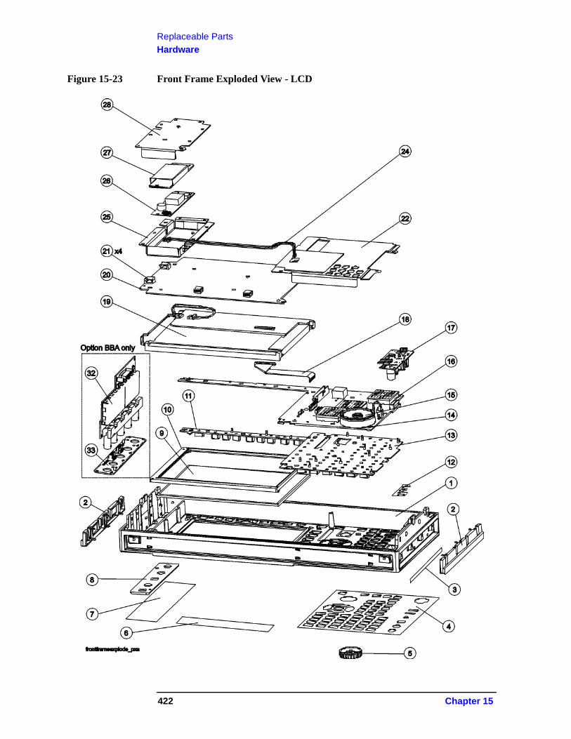
Replaceable Parts
Hardware
Figure 15-23 Front Frame Exploded View - LCD
422 Chapter 15
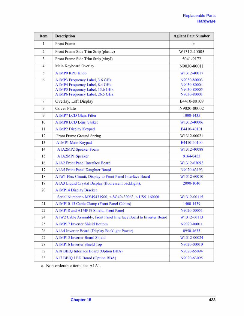
Replaceable Parts
Hardware
Item Description Agilent Part Number
1 Front Frame ---a
2 Front Frame Side Trim Strip (plastic) W1312-40005
3 Front Frame Side Trim Strip (vinyl) 5041-9172
4 Main Keyboard Overlay N9030-80011
5 A1MP9 RPG Knob W1312-40017
6 A1MP3 Frequency Label, 3.6 GHzA1MP4 Frequency Label, 8.4 GHzA1MP5 Frequency Label, 13.6 GHzA1MP6 Frequency Label, 26.5 GHz
N9030-80003N9030-80004N9030-80005N9030-80001
7 Overlay, Left Display E4410-80109
8 Cover Plate N9020-00002
9 A1MP7 LCD Glass Filter 1000-1435
10 A1MP8 LCD Lens Gasket W1312-40006
11 A1MP2 Display Keypad E4410-40101
12 Front Frame Ground Spring W1312-00021
13 A1MP1 Main Keypad E4410-40100
14 A1A2MP2 Speaker Foam W1312-40088
15 A1A2MP1 Speaker 9164-0453
16 A1A2 Front Panel Interface Board W1312-63092
17 A1A5 Front Panel Daughter Board N9020-63193
18 A1W1 Flex Circuit, Display to Front Panel Interface Board W1312-60010
19 A1A3 Liquid Crystal Display (fluorescent backlight), 2090-1040
20 A1MP14 Display Bracket
Serial Number < MY49431900, < SG49430063, < US51160001 W1312-00115
21 A1MP10-13 Cable Clamp (Front Panel Cables) 1400-1439
22 A1MP18 and A1MP19 Shield, Front Panel N9020-00051
24 A1W2 Cable Assembly, Front Panel Interface Board to Inverter Board W1312-60113
25 A1MP17 Inverter Shield Bottom N9020-00011
26 A1A4 Inverter Board (Display Backlight Power) 0950-4635
27 A1MP15 Inverter Board Shield W1312-00024
28 A1MP16 Inverter Shield Top N9020-00010
32 A18 BBIQ Interface Board (Option BBA) N9020-65094
33 A17 BBIQ LED Board (Option BBA) N9020-63095
a. Non-orderable item, see A1A1.
Chapter 15 423
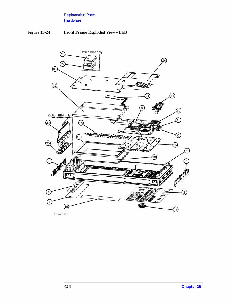
Replaceable Parts
Hardware
Figure 15-24 Front Frame Exploded View - LED
424 Chapter 15
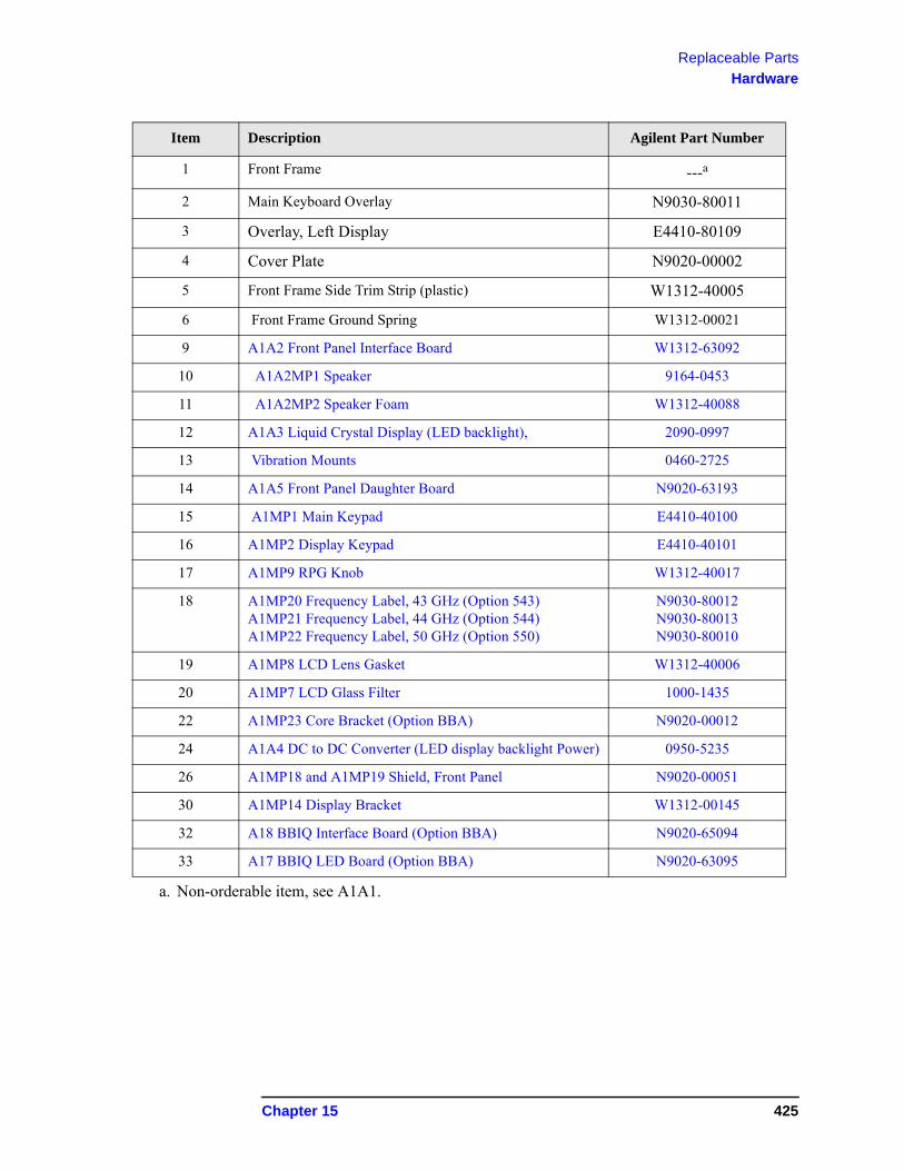
Replaceable Parts
Hardware
Item Description Agilent Part Number
1 Front Frame ---a
2 Main Keyboard Overlay N9030-80011
3 Overlay, Left Display E4410-80109
4 Cover Plate N9020-00002
5 Front Frame Side Trim Strip (plastic) W1312-40005
6 Front Frame Ground Spring W1312-00021
9 A1A2 Front Panel Interface Board W1312-63092
10 A1A2MP1 Speaker 9164-0453
11 A1A2MP2 Speaker Foam W1312-40088
12 A1A3 Liquid Crystal Display (LED backlight), 2090-0997
13 Vibration Mounts 0460-2725
14 A1A5 Front Panel Daughter Board N9020-63193
15 A1MP1 Main Keypad E4410-40100
16 A1MP2 Display Keypad E4410-40101
17 A1MP9 RPG Knob W1312-40017
18 A1MP20 Frequency Label, 43 GHz (Option 543)A1MP21 Frequency Label, 44 GHz (Option 544)A1MP22 Frequency Label, 50 GHz (Option 550)
N9030-80012N9030-80013N9030-80010
19 A1MP8 LCD Lens Gasket W1312-40006
20 A1MP7 LCD Glass Filter 1000-1435
22 A1MP23 Core Bracket (Option BBA) N9020-00012
24 A1A4 DC to DC Converter (LED display backlight Power) 0950-5235
26 A1MP18 and A1MP19 Shield, Front Panel N9020-00051
30 A1MP14 Display Bracket W1312-00145
32 A18 BBIQ Interface Board (Option BBA) N9020-65094
33 A17 BBIQ LED Board (Option BBA) N9020-63095
a. Non-orderable item, see A1A1.
Chapter 15 425

Replaceable Parts
Hardware
426 Chapter 15
16 Assembly Replacement Procedures
427
Assembly Replacement Procedures
What You Will Find in This Chapter
What You Will Find in This Chapter
Procedures in this chapter enable you to locate, remove, and replace the following major assemblies in your instrument.
Refer to Chapter 15 , “Replaceable Parts,” for part numbers, assembly descriptions, and ordering information.
Instrument Outer Case on page 432
Top Brace and Power Supply Bracket on page 434
RF Area (Options 503, 508, 513, 526) on page 436
Microwave Options MPB and LNP on page 449
RF Area (Options 543, 544, 550) on page 471
Millimeter Wave Options MPB and LNP on page 483
RF Front End Assembly on page 491
Front End Control Assembly on page 494
LO Synthesizer Assembly on page 496
Reference Assembly on page 498
Option B1X on page 501
Option BBA on page 503
Midplane Board Assembly on page 504
Rear Panel on page 506
Power Supply Assembly on page 507
CPU Assembly on page 509
Disk Drive on page 510
AIF/DIF Assembly on page 516
Motherboard Assembly on page 520
Fan Assembly on page 525
Input Connector Assembly on page 529
Front Frame Assembly on page 531
Inverter Board Assembly on page 538
Display Assembly - LCD on page 539
Display Assembly - LED on page 547
Daughter Board, Interface Board and Keypad on page 541 and page 549
428 Chapter 16
Assembly Replacement Procedures
What You Will Find in This Chapter
Before Starting
Before starting to disassemble the instrument:
• Check that you are familiar with the safety symbols marked on the instrument. And, read the general safety considerations and the safety note definitions given in the front of this guide.
• The instrument contains static sensitive components. Read the section entitled “ESD Information” on page 25.
Safety
WARNING The opening of covers or removal of parts is likely to expose dangerous voltages. Disconnect the product from all voltage sources while it is being opened.
WARNING The instrument contains potentially hazardous voltages. Refer to the safety symbols on the instrument and the general safety considerations at the beginning of this service guide before operating the unit with the cover removed. Failure to heed the safety precautions can result in severe or fatal injury.
Chapter 16 429
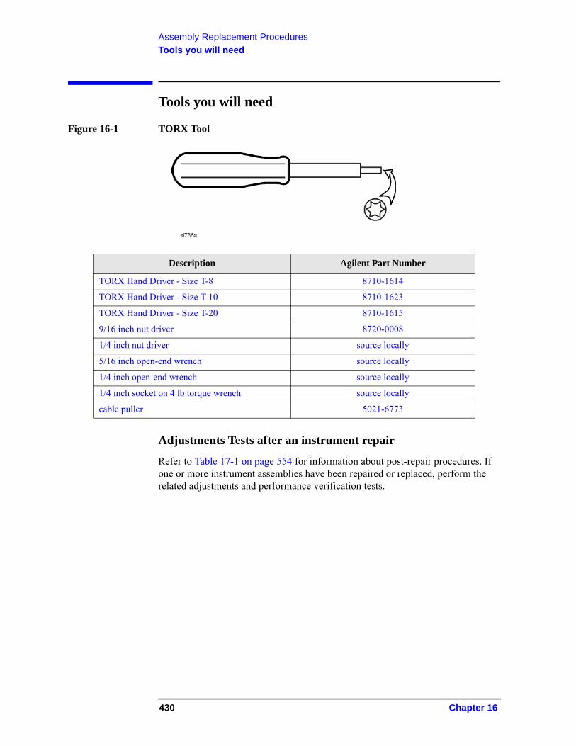
Assembly Replacement Procedures
Tools you will need
Tools you will need
Figure 16-1 TORX Tool
Adjustments Tests after an instrument repair
Refer to Table 17-1 on page 554 for information about post-repair procedures. If one or more instrument assemblies have been repaired or replaced, perform the related adjustments and performance verification tests.
Description Agilent Part Number
TORX Hand Driver - Size T-8 8710-1614
TORX Hand Driver - Size T-10 8710-1623
TORX Hand Driver - Size T-20 8710-1615
9/16 inch nut driver 8720-0008
1/4 inch nut driver source locally
5/16 inch open-end wrench source locally
1/4 inch open-end wrench source locally
1/4 inch socket on 4 lb torque wrench source locally
cable puller 5021-6773
430 Chapter 16
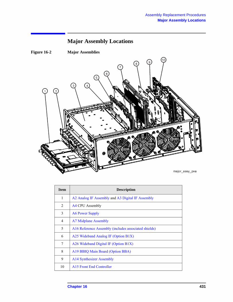
Assembly Replacement Procedures
Major Assembly Locations
Major Assembly Locations
Figure 16-2 Major Assemblies
Item Description
1 A2 Analog IF Assembly and A3 Digital IF Assembly
2 A4 CPU Assembly
3 A6 Power Supply
4 A7 Midplane Assembly
5 A16 Reference Assembly (includes associated shields)
6 A25 Wideband Analog IF (Option B1X)
7 A26 Wideband Digital IF (Option B1X)
8 A19 BBIQ Main Board (Option BBA)
9 A14 Synthesizer Assembly
10 A15 Front End Controller
Chapter 16 431
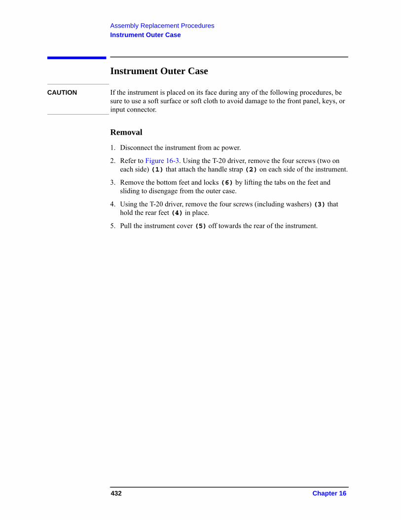
Assembly Replacement Procedures
Instrument Outer Case
Instrument Outer Case
CAUTION If the instrument is placed on its face during any of the following procedures, be sure to use a soft surface or soft cloth to avoid damage to the front panel, keys, or input connector.
Removal
1. Disconnect the instrument from ac power.
2. Refer to Figure 16-3. Using the T-20 driver, remove the four screws (two on each side) (1) that attach the handle strap (2) on each side of the instrument.
3. Remove the bottom feet and locks (6) by lifting the tabs on the feet and sliding to disengage from the outer case.
4. Using the T-20 driver, remove the four screws (including washers) (3) that hold the rear feet (4) in place.
5. Pull the instrument cover (5) off towards the rear of the instrument.
432 Chapter 16
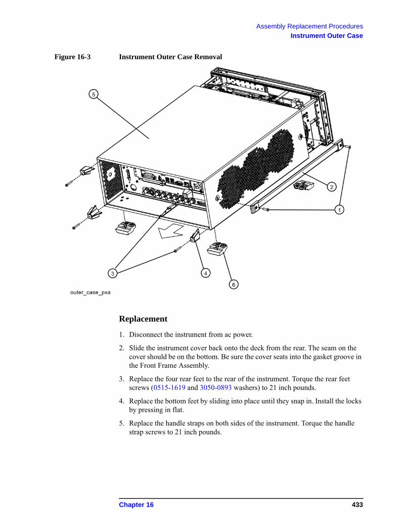
Assembly Replacement Procedures
Instrument Outer Case
Figure 16-3 Instrument Outer Case Removal
Replacement
1. Disconnect the instrument from ac power.
2. Slide the instrument cover back onto the deck from the rear. The seam on the cover should be on the bottom. Be sure the cover seats into the gasket groove in the Front Frame Assembly.
3. Replace the four rear feet to the rear of the instrument. Torque the rear feet screws (0515-1619 and 3050-0893 washers) to 21 inch pounds.
4. Replace the bottom feet by sliding into place until they snap in. Install the locks by pressing in flat.
5. Replace the handle straps on both sides of the instrument. Torque the handle strap screws to 21 inch pounds.
Chapter 16 433
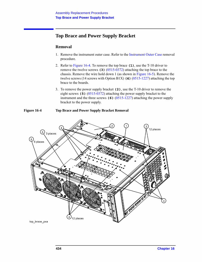
Assembly Replacement Procedures
Top Brace and Power Supply Bracket
Top Brace and Power Supply Bracket
Removal
1. Remove the instrument outer case. Refer to the Instrument Outer Case removal procedure.
2. Refer to Figure 16-4. To remove the top brace (1), use the T-10 driver to remove the twelve screws (3) (0515-0372) attaching the top brace to the chassis. Remove the wire hold down 1 (as shown in Figure 16-5). Remove the twelve screws (14 screws with Option B1X) (4) (0515-1227) attaching the top brace to the boards.
3. To remove the power supply bracket (2), use the T-10 driver to remove the eight screws (5) (0515-0372) attaching the power supply bracket to the instrument and the three screws (6) (0515-1227) attaching the power supply bracket to the power supply.
Figure 16-4 Top Brace and Power Supply Bracket Removal
434 Chapter 16
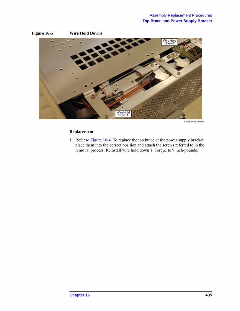
Assembly Replacement Procedures
Top Brace and Power Supply Bracket
Figure 16-5 Wire Hold Downs
Replacement
1. Refer to Figure 16-4. To replace the top brace or the power supply bracket, place them into the correct position and attach the screws referred to in the removal process. Reinstall wire hold down 1. Torque to 9 inch-pounds.
Chapter 16 435
Assembly Replacement Procedures
RF Area (Options 503, 508, 513, 526)
RF Area (Options 503, 508, 513, 526)
Refer to Figure 16-6. The RF area consists of RF attenuator A (1), RF attenuator B (2), low band switch assembly (3), YTF Preselector (4), and YTO (5).
Figure 16-6 RF Area Components and Cables(Options 503, 508, 513, 526)
To gain access to the attenuators, low band switch, YTF Preselector, YTO, Option MPB, or Option LNP for removal, follow these steps:
1. Remove the instrument outer case. Refer to the Instrument Outer Case removal procedure.
2. Remove the front panel. Refer to the Front Frame Assembly removal procedure.
436 Chapter 16
Assembly Replacement Procedures
RF Area (Options 503, 508, 513, 526)
3. Refer to Figure 16-7. Remove the RF bracket (1) by removing the sixteen screws (2) (0515-0372) using the T-10 driver.
Figure 16-7 RF Bracket Removal
Chapter 16 437
Assembly Replacement Procedures
RF Area (Options 503, 508, 513, 526)
Attenuators
Removal
1. Refer to Figure 16-8. To remove Attenuator A (1) or Attenuator B (2), remove the semi-rigid cables W2, W3, W4, or W6 attached to the attenuator using the 5/16 inch wrench.
2. Remove the ribbon cable attached to the attenuator.
3. Remove the two screws (3) or (4) (0515-0372) for each attenuator bracket to remove from the chassis using the T-10 driver.
4. Remove the attenuator from the bracket by removing the two screws (0515-0372).
438 Chapter 16
Assembly Replacement Procedures
RF Area (Options 503, 508, 513, 526)
Figure 16-8 Attenuators Removal
Item Agilent Part Number
W2 N9020-20100
W3 N9020-20023
W4 N9020-20025
W6 N9020-20024
Chapter 16 439
Assembly Replacement Procedures
RF Area (Options 503, 508, 513, 526)
Replacement
1. Refer to Figure 16-8. Position the attenuator in the bracket so that the ribbon connector end is “up”.
2. Replace the two screws (0515-0372) that attach the attenuator to the bracket. Torque to 9 inch-pounds.
3. Position the attenuator and bracket into the chassis and attach with the two screws (0515-0372). Torque to 9 inch-pounds.
4. Replace the ribbon cable and semi-rigid cables W2, W3, W4, or W6 to the attenuator. Torque the semi-rigid cables to 10 inch-pounds.
5. Refer to Figure 16-7. Position the RF bracket onto the chassis and replace the sixteen screws (0515-0372). Torque to 9 inch-pounds.
6. Replace the front panel. Refer to the Front Frame Assembly replacement procedure.
7. Replace the instrument outer case. Refer to the Instrument Outer Case replacement procedure.
440 Chapter 16
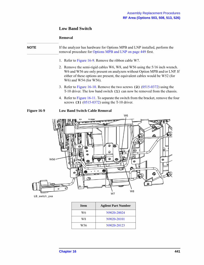
Assembly Replacement Procedures
RF Area (Options 503, 508, 513, 526)
Low Band Switch
Removal
NOTE If the analyzer has hardware for Options MPB and LNP installed, perform the removal procedure for Options MPB and LNP on page 449 first.
1. Refer to Figure 16-9. Remove the ribbon cable W7.
2. Remove the semi-rigid cables W6, W8, and W56 using the 5/16 inch wrench. W6 and W56 are only present on analyzers without Option MPB and/or LNP. If either of these options are present, the equivalent cables would be W52 (for W6) and W54 (for W56).
3. Refer to Figure 16-10. Remove the two screws (2) (0515-0372) using the T-10 driver. The low band switch (1) can now be removed from the chassis.
4. Refer to Figure 16-11. To separate the switch from the bracket, remove the four screws (3) (0515-0372) using the T-10 driver.
Figure 16-9 Low Band Switch Cable Removal
Item Agilent Part Number
W6 N9020-20024
W8 N9020-20101
W56 N9020-20123
Chapter 16 441
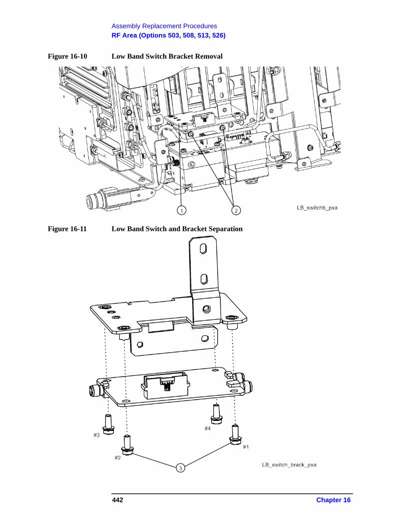
Assembly Replacement Procedures
RF Area (Options 503, 508, 513, 526)
Figure 16-10 Low Band Switch Bracket Removal
Figure 16-11 Low Band Switch and Bracket Separation
442 Chapter 16
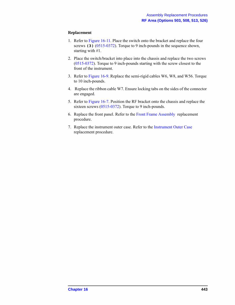
Assembly Replacement Procedures
RF Area (Options 503, 508, 513, 526)
Replacement
1. Refer to Figure 16-11. Place the switch onto the bracket and replace the four screws (3) (0515-0372). Torque to 9 inch-pounds in the sequence shown, starting with #1.
2. Place the switch/bracket into place into the chassis and replace the two screws (0515-0372). Torque to 9 inch-pounds starting with the screw closest to the front of the instrument.
3. Refer to Figure 16-9. Replace the semi-rigid cables W6, W8, and W56. Torque to 10 inch-pounds.
4. Replace the ribbon cable W7. Ensure locking tabs on the sides of the connector are engaged.
5. Refer to Figure 16-7. Position the RF bracket onto the chassis and replace the sixteen screws (0515-0372). Torque to 9 inch-pounds.
6. Replace the front panel. Refer to the Front Frame Assembly replacement procedure.
7. Replace the instrument outer case. Refer to the Instrument Outer Case replacement procedure.
Chapter 16 443
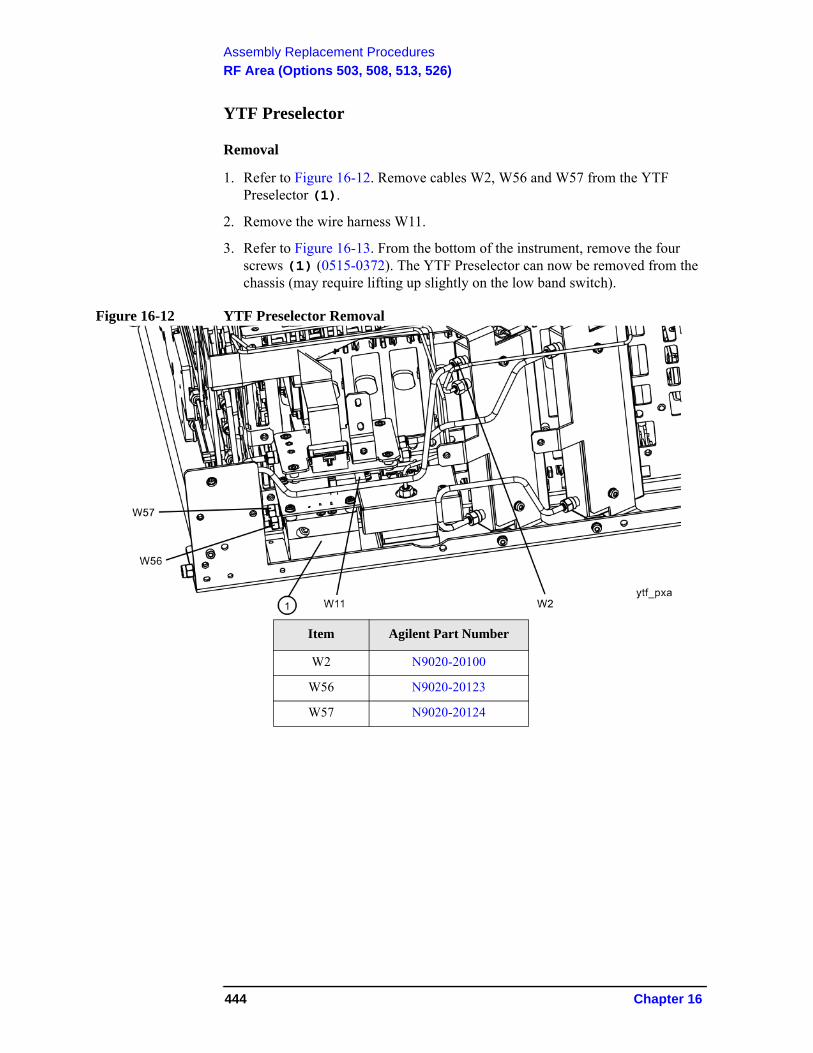
Assembly Replacement Procedures
RF Area (Options 503, 508, 513, 526)
YTF Preselector
Removal
1. Refer to Figure 16-12. Remove cables W2, W56 and W57 from the YTF Preselector (1).
2. Remove the wire harness W11.
3. Refer to Figure 16-13. From the bottom of the instrument, remove the four screws (1) (0515-0372). The YTF Preselector can now be removed from the chassis (may require lifting up slightly on the low band switch).
Figure 16-12 YTF Preselector Removal
Item Agilent Part Number
W2 N9020-20100
W56 N9020-20123
W57 N9020-20124
444 Chapter 16
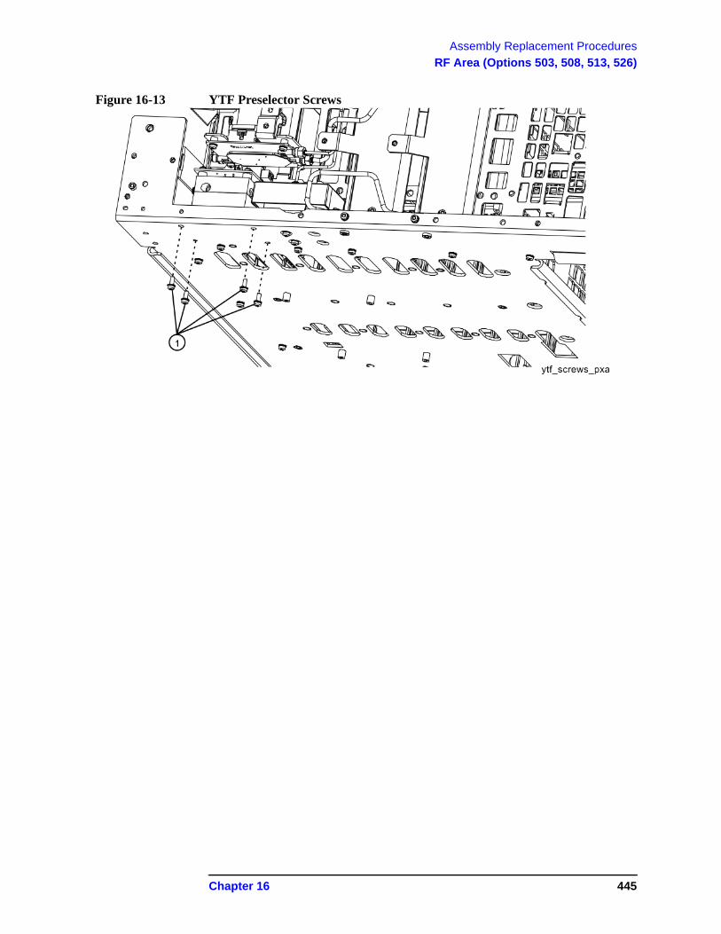
Assembly Replacement Procedures
RF Area (Options 503, 508, 513, 526)
Figure 16-13 YTF Preselector Screws
Chapter 16 445
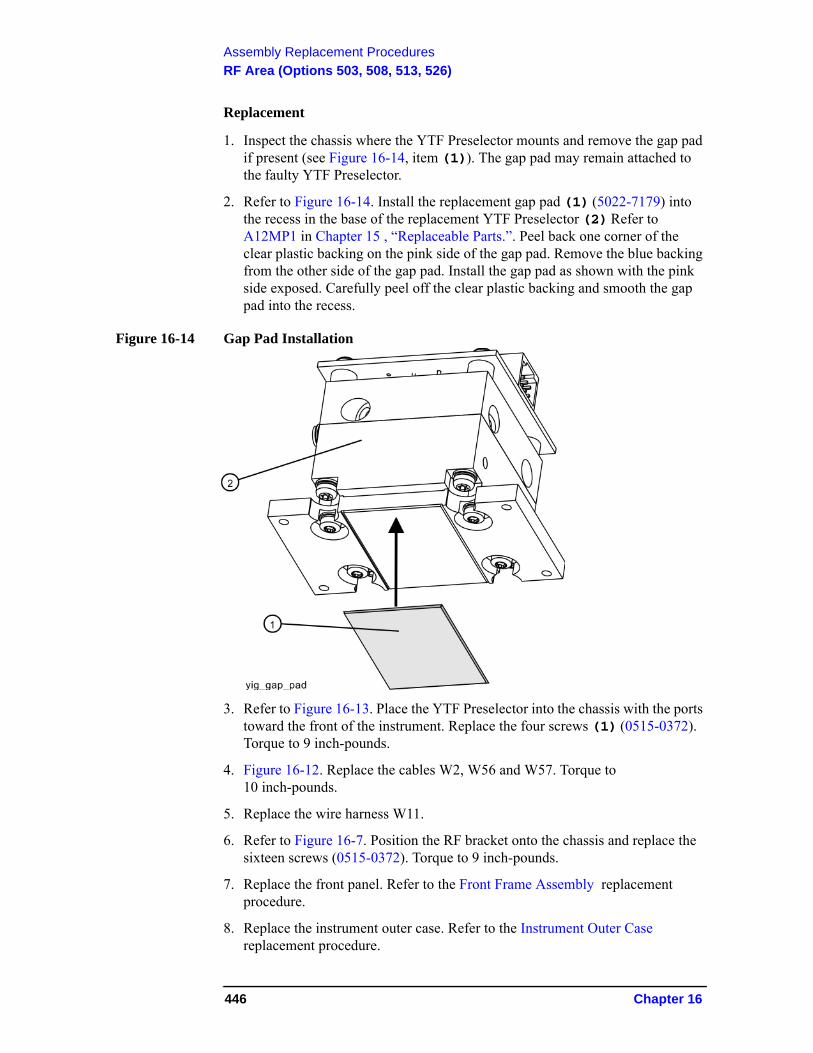
Assembly Replacement Procedures
RF Area (Options 503, 508, 513, 526)
Replacement
1. Inspect the chassis where the YTF Preselector mounts and remove the gap pad if present (see Figure 16-14, item (1)). The gap pad may remain attached to the faulty YTF Preselector.
2. Refer to Figure 16-14. Install the replacement gap pad (1) (5022-7179) into the recess in the base of the replacement YTF Preselector (2) Refer to A12MP1 in Chapter 15 , “Replaceable Parts.”. Peel back one corner of the clear plastic backing on the pink side of the gap pad. Remove the blue backing from the other side of the gap pad. Install the gap pad as shown with the pink side exposed. Carefully peel off the clear plastic backing and smooth the gap pad into the recess.
Figure 16-14 Gap Pad Installation
3. Refer to Figure 16-13. Place the YTF Preselector into the chassis with the ports toward the front of the instrument. Replace the four screws (1) (0515-0372). Torque to 9 inch-pounds.
4. Figure 16-12. Replace the cables W2, W56 and W57. Torque to 10 inch-pounds.
5. Replace the wire harness W11.
6. Refer to Figure 16-7. Position the RF bracket onto the chassis and replace the sixteen screws (0515-0372). Torque to 9 inch-pounds.
7. Replace the front panel. Refer to the Front Frame Assembly replacement procedure.
8. Replace the instrument outer case. Refer to the Instrument Outer Case replacement procedure.
446 Chapter 16
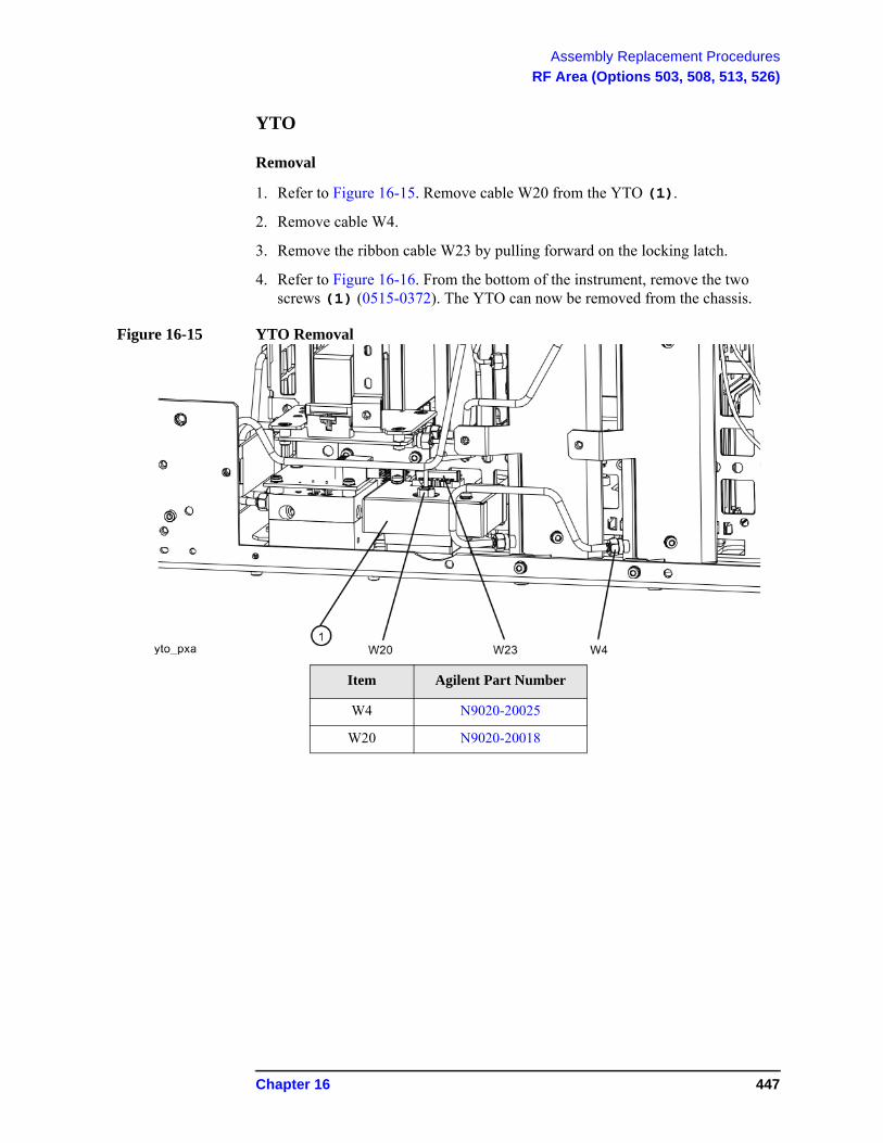
Assembly Replacement Procedures
RF Area (Options 503, 508, 513, 526)
YTO
Removal
1. Refer to Figure 16-15. Remove cable W20 from the YTO (1).
2. Remove cable W4.
3. Remove the ribbon cable W23 by pulling forward on the locking latch.
4. Refer to Figure 16-16. From the bottom of the instrument, remove the two screws (1) (0515-0372). The YTO can now be removed from the chassis.
Figure 16-15 YTO Removal
Item Agilent Part Number
W4 N9020-20025
W20 N9020-20018
Chapter 16 447
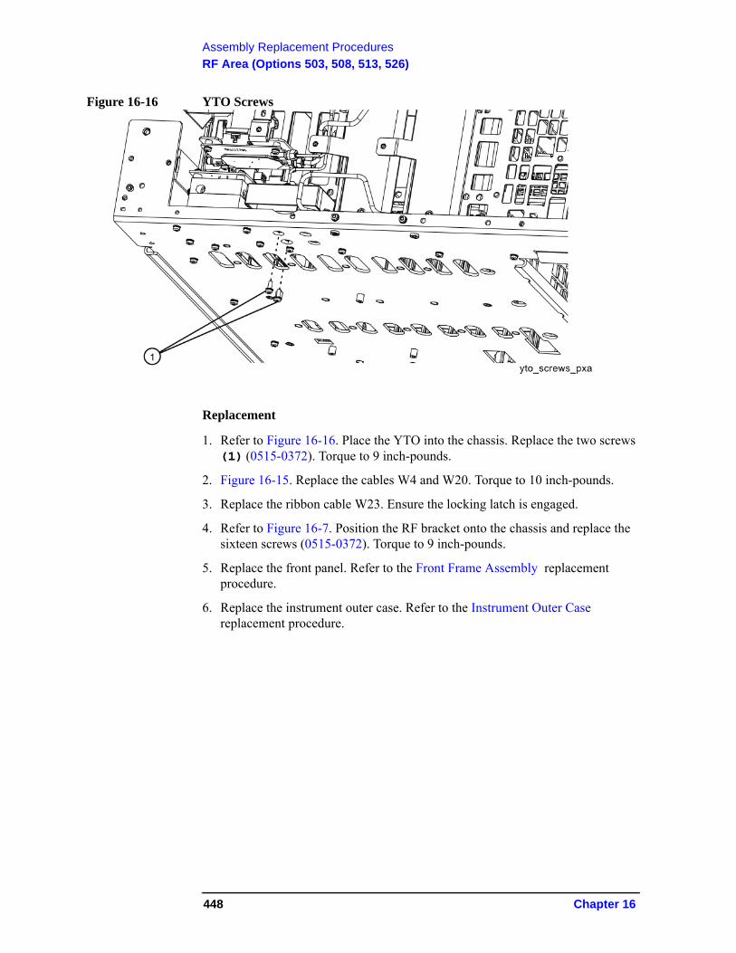
Assembly Replacement Procedures
RF Area (Options 503, 508, 513, 526)
Figure 16-16 YTO Screws
Replacement
1. Refer to Figure 16-16. Place the YTO into the chassis. Replace the two screws (1) (0515-0372). Torque to 9 inch-pounds.
2. Figure 16-15. Replace the cables W4 and W20. Torque to 10 inch-pounds.
3. Replace the ribbon cable W23. Ensure the locking latch is engaged.
4. Refer to Figure 16-7. Position the RF bracket onto the chassis and replace the sixteen screws (0515-0372). Torque to 9 inch-pounds.
5. Replace the front panel. Refer to the Front Frame Assembly replacement procedure.
6. Replace the instrument outer case. Refer to the Instrument Outer Case replacement procedure.
448 Chapter 16
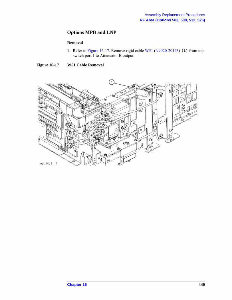
Assembly Replacement Procedures
RF Area (Options 503, 508, 513, 526)
Options MPB and LNP
Removal
1. Refer to Figure 16-17. Remove rigid cable W51 (N9020-20143) (1) from top switch port 1 to Attenuator B output.
Figure 16-17 W51 Cable Removal
Chapter 16 449
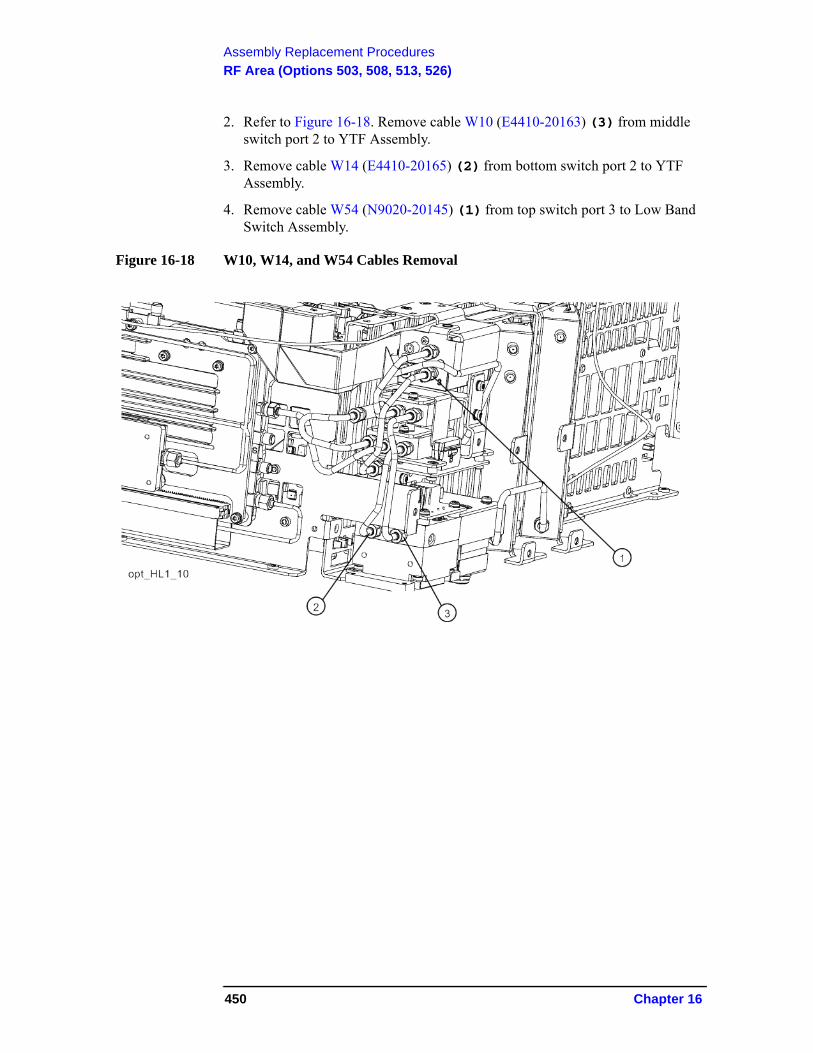
Assembly Replacement Procedures
RF Area (Options 503, 508, 513, 526)
2. Refer to Figure 16-18. Remove cable W10 (E4410-20163) (3) from middle switch port 2 to YTF Assembly.
3. Remove cable W14 (E4410-20165) (2) from bottom switch port 2 to YTF Assembly.
4. Remove cable W54 (N9020-20145) (1) from top switch port 3 to Low Band Switch Assembly.
Figure 16-18 W10, W14, and W54 Cables Removal
450 Chapter 16
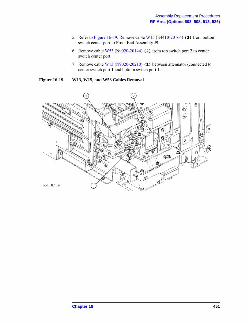
Assembly Replacement Procedures
RF Area (Options 503, 508, 513, 526)
5. Refer to Figure 16-19. Remove cable W15 (E4410-20164) (3) from bottom switch center port to Front End Assembly J9.
6. Remove cable W53 (N9020-20144) (2) from top switch port 2 to center switch center port.
7. Remove cable W13 (N9020-20210) (1) between attenuator (connected to center switch port 1 and bottom switch port 1.
Figure 16-19 W13, W15, and W53 Cables Removal
Chapter 16 451
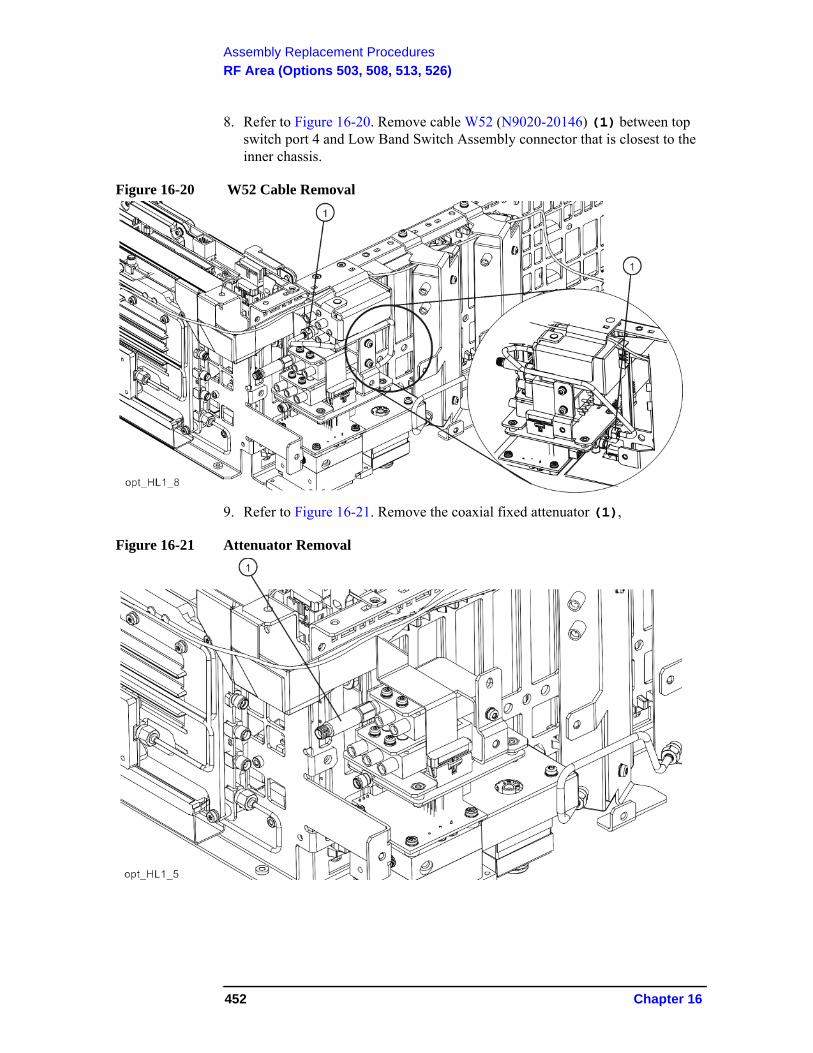
Assembly Replacement Procedures
RF Area (Options 503, 508, 513, 526)
8. Refer to Figure 16-20. Remove cable W52 (N9020-20146) (1) between top switch port 4 and Low Band Switch Assembly connector that is closest to the inner chassis.
Figure 16-20 W52 Cable Removal
9. Refer to Figure 16-21. Remove the coaxial fixed attenuator (1),
Figure 16-21 Attenuator Removal
452 Chapter 16
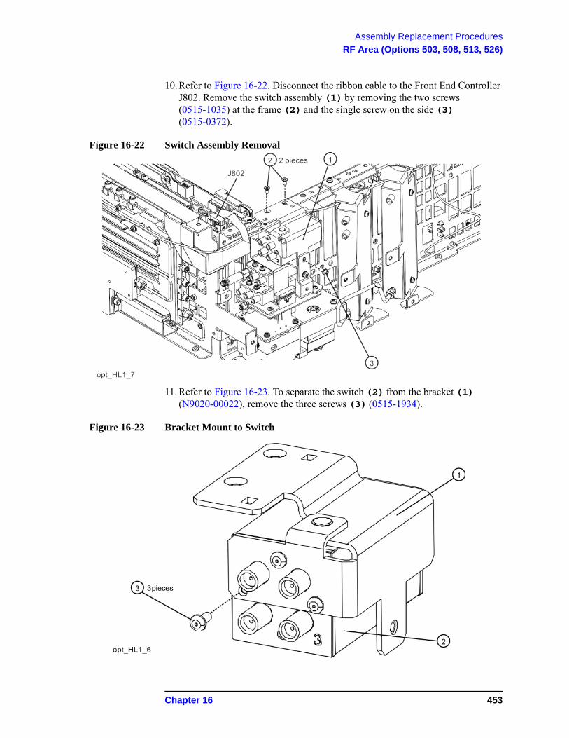
Assembly Replacement Procedures
RF Area (Options 503, 508, 513, 526)
10.Refer to Figure 16-22. Disconnect the ribbon cable to the Front End Controller J802. Remove the switch assembly (1) by removing the two screws (0515-1035) at the frame (2) and the single screw on the side (3) (0515-0372).
Figure 16-22 Switch Assembly Removal
11. Refer to Figure 16-23. To separate the switch (2) from the bracket (1) (N9020-00022), remove the three screws (3) (0515-1934).
Figure 16-23 Bracket Mount to Switch
Chapter 16 453
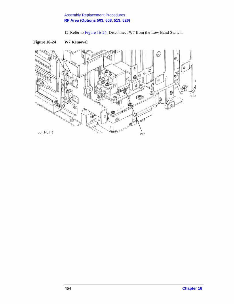
Assembly Replacement Procedures
RF Area (Options 503, 508, 513, 526)
12.Refer to Figure 16-24. Disconnect W7 from the Low Band Switch.
Figure 16-24 W7 Removal
454 Chapter 16
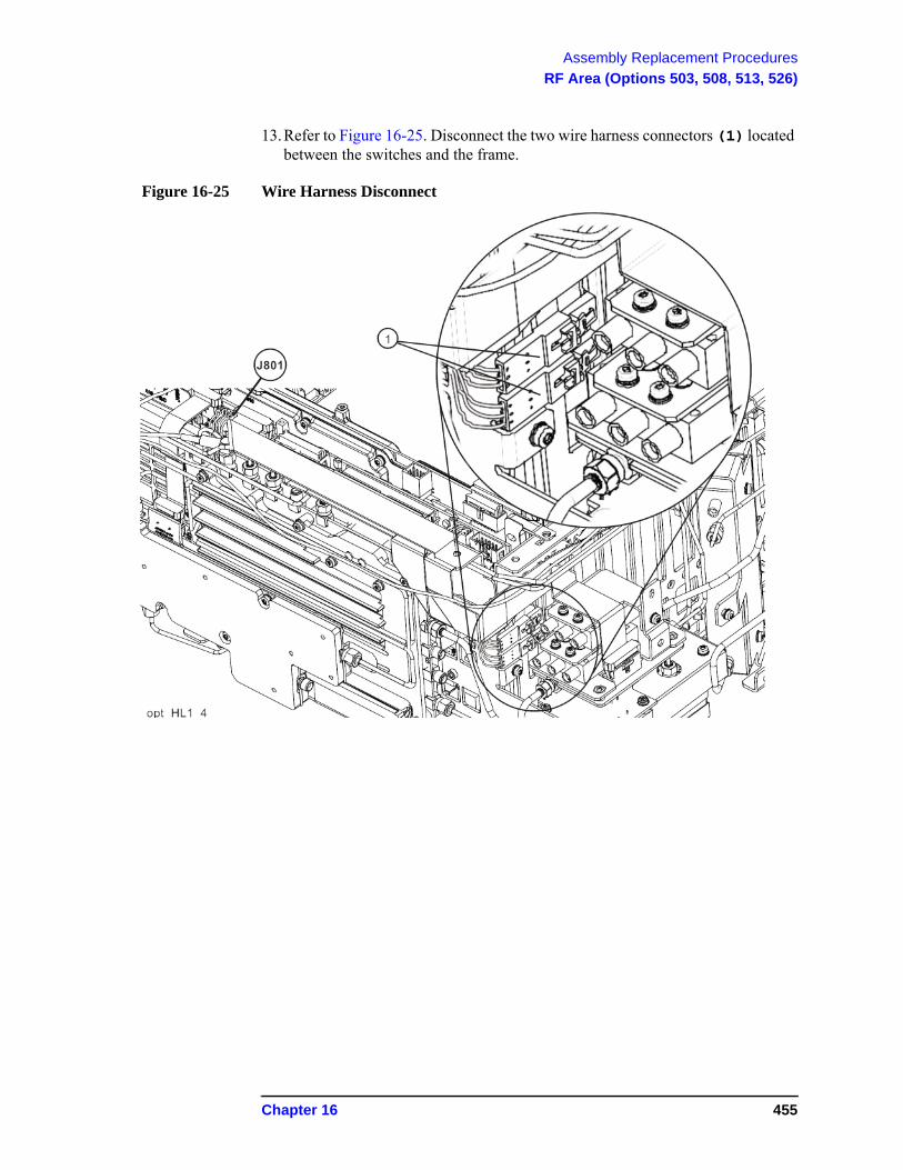
Assembly Replacement Procedures
RF Area (Options 503, 508, 513, 526)
13.Refer to Figure 16-25. Disconnect the two wire harness connectors (1) located between the switches and the frame.
Figure 16-25 Wire Harness Disconnect
Chapter 16 455
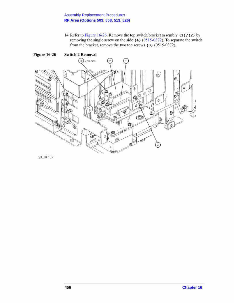
Assembly Replacement Procedures
RF Area (Options 503, 508, 513, 526)
14.Refer to Figure 16-26. Remove the top switch/bracket assembly (1)/(2) by removing the single screw on the side (4) (0515-0372). To separate the switch from the bracket, remove the two top screws (3) (0515-0372).
Figure 16-26 Switch 2 Removal
456 Chapter 16
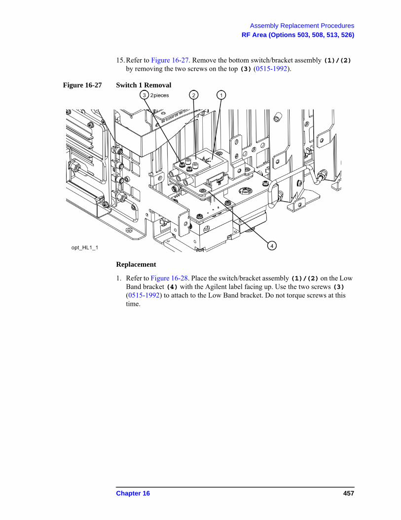
Assembly Replacement Procedures
RF Area (Options 503, 508, 513, 526)
15.Refer to Figure 16-27. Remove the bottom switch/bracket assembly (1)/(2) by removing the two screws on the top (3) (0515-1992).
Figure 16-27 Switch 1 Removal
Replacement
1. Refer to Figure 16-28. Place the switch/bracket assembly (1)/(2) on the Low Band bracket (4) with the Agilent label facing up. Use the two screws (3) (0515-1992) to attach to the Low Band bracket. Do not torque screws at this time.
Chapter 16 457
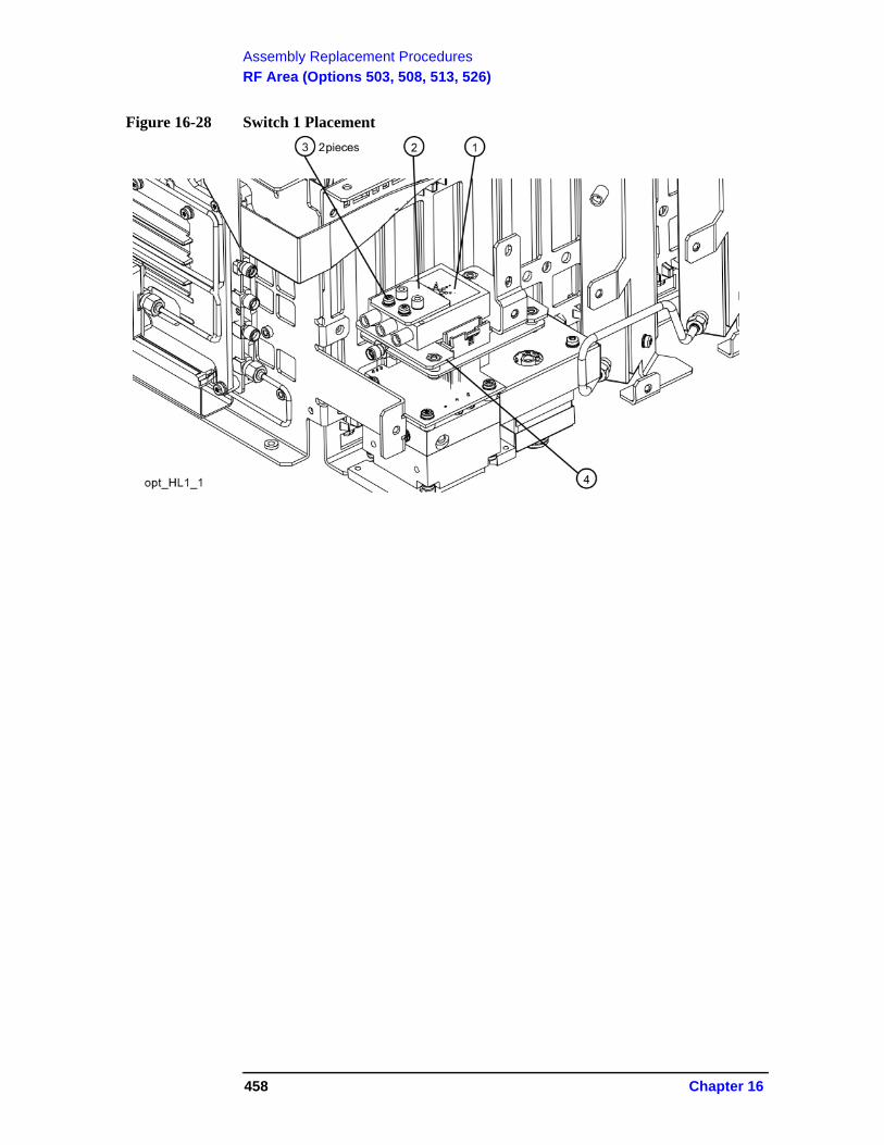
Assembly Replacement Procedures
RF Area (Options 503, 508, 513, 526)
Figure 16-28 Switch 1 Placement
458 Chapter 16
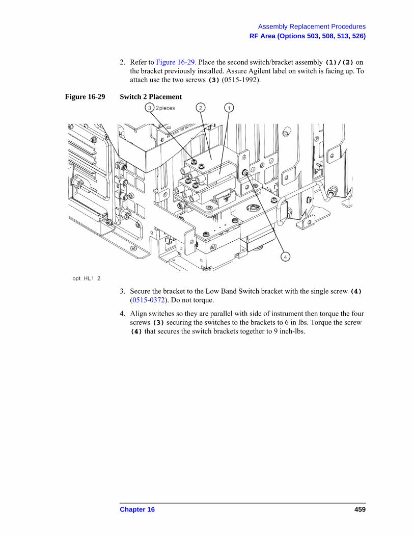
Assembly Replacement Procedures
RF Area (Options 503, 508, 513, 526)
2. Refer to Figure 16-29. Place the second switch/bracket assembly (1)/(2) on the bracket previously installed. Assure Agilent label on switch is facing up. To attach use the two screws (3) (0515-1992).
Figure 16-29 Switch 2 Placement
3. Secure the bracket to the Low Band Switch bracket with the single screw (4) (0515-0372). Do not torque.
4. Align switches so they are parallel with side of instrument then torque the four screws (3) securing the switches to the brackets to 6 in lbs. Torque the screw (4) that secures the switch brackets together to 9 inch-lbs.
Chapter 16 459
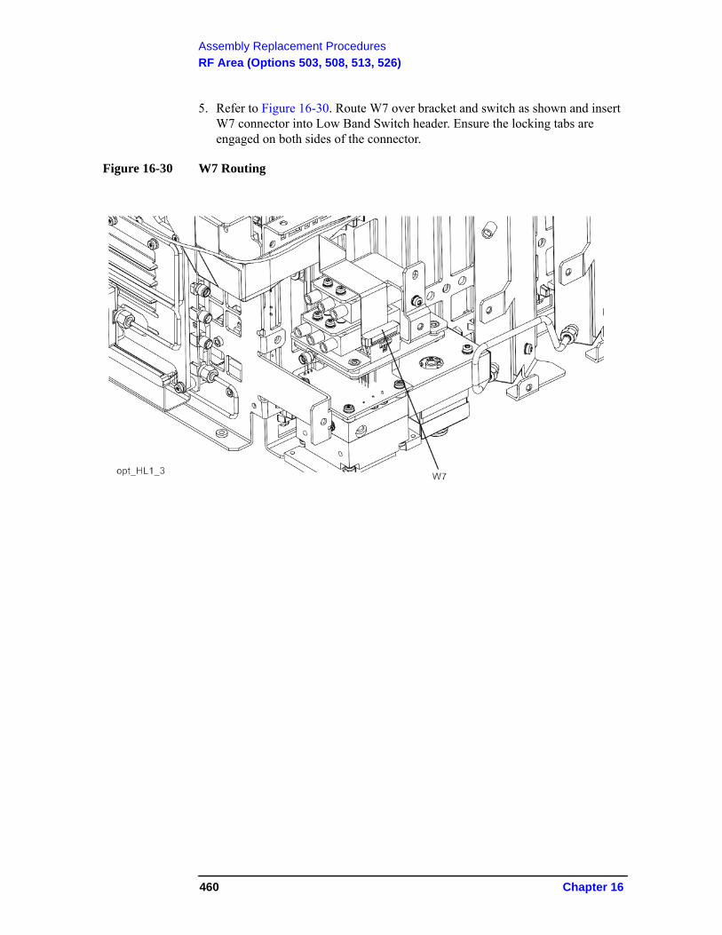
Assembly Replacement Procedures
RF Area (Options 503, 508, 513, 526)
5. Refer to Figure 16-30. Route W7 over bracket and switch as shown and insert W7 connector into Low Band Switch header. Ensure the locking tabs are engaged on both sides of the connector.
Figure 16-30 W7 Routing
460 Chapter 16

Assembly Replacement Procedures
RF Area (Options 503, 508, 513, 526)
6. Refer to Figure 16-31. Reconnect the two wire harness connectors (1). Once connected, position the connections along side the switches.
Figure 16-31 Wire Harness Routing
Chapter 16 461
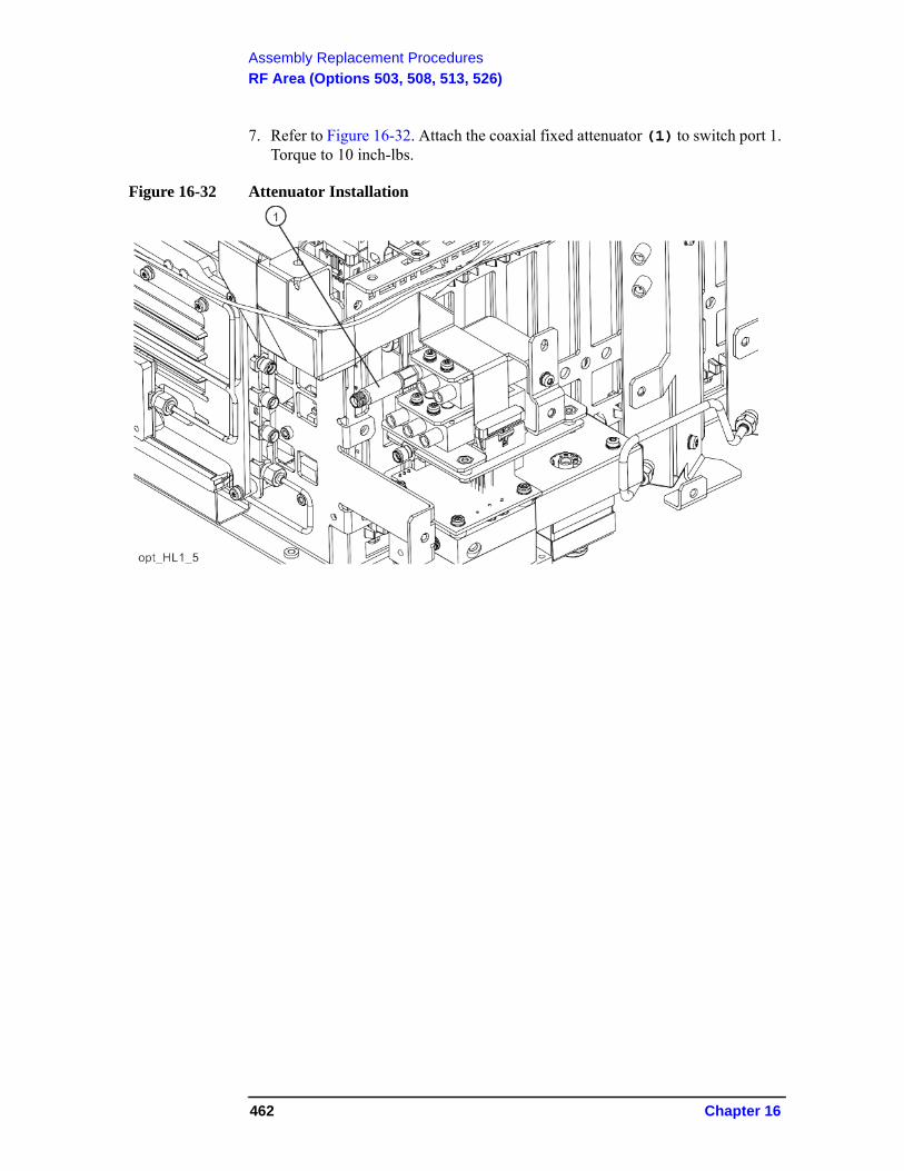
Assembly Replacement Procedures
RF Area (Options 503, 508, 513, 526)
7. Refer to Figure 16-32. Attach the coaxial fixed attenuator (1) to switch port 1. Torque to 10 inch-lbs.
Figure 16-32 Attenuator Installation
462 Chapter 16
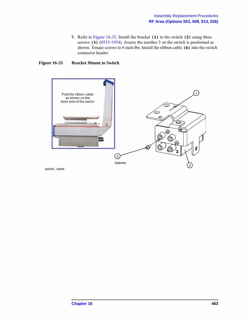
Assembly Replacement Procedures
RF Area (Options 503, 508, 513, 526)
8. Refer to Figure 16-33. Install the bracket (1) to the switch (2) using three screws (3) (0515-1934). Assure the number 3 on the switch is positioned as shown. Torque screws to 6 inch-lbs. Install the ribbon cable (4) into the switch connector header.
Figure 16-33 Bracket Mount to Switch
Chapter 16 463
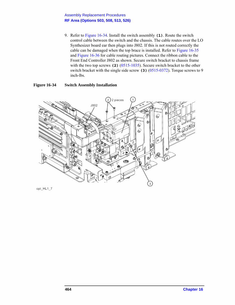
Assembly Replacement Procedures
RF Area (Options 503, 508, 513, 526)
9. Refer to Figure 16-34. Install the switch assembly (1). Route the switch control cable between the switch and the chassis. The cable routes over the LO Synthesizer board ear then plugs into J802. If this is not routed correctly the cable can be damaged when the top brace is installed. Refer to Figure 16-35 and Figure 16-36 for cable routing pictures. Connect the ribbon cable to the Front End Controller J802 as shown. Secure switch bracket to chassis frame with the two top screws (2) (0515-1035). Secure switch bracket to the other switch bracket with the single side screw (3) (0515-0372). Torque screws to 9 inch-lbs.
Figure 16-34 Switch Assembly Installation
464 Chapter 16
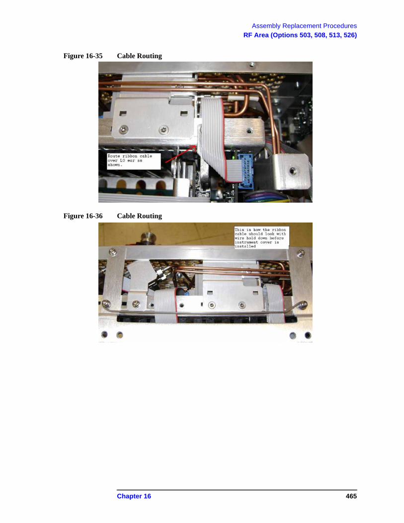
Assembly Replacement Procedures
RF Area (Options 503, 508, 513, 526)
Figure 16-35 Cable Routing
Figure 16-36 Cable Routing
Chapter 16 465
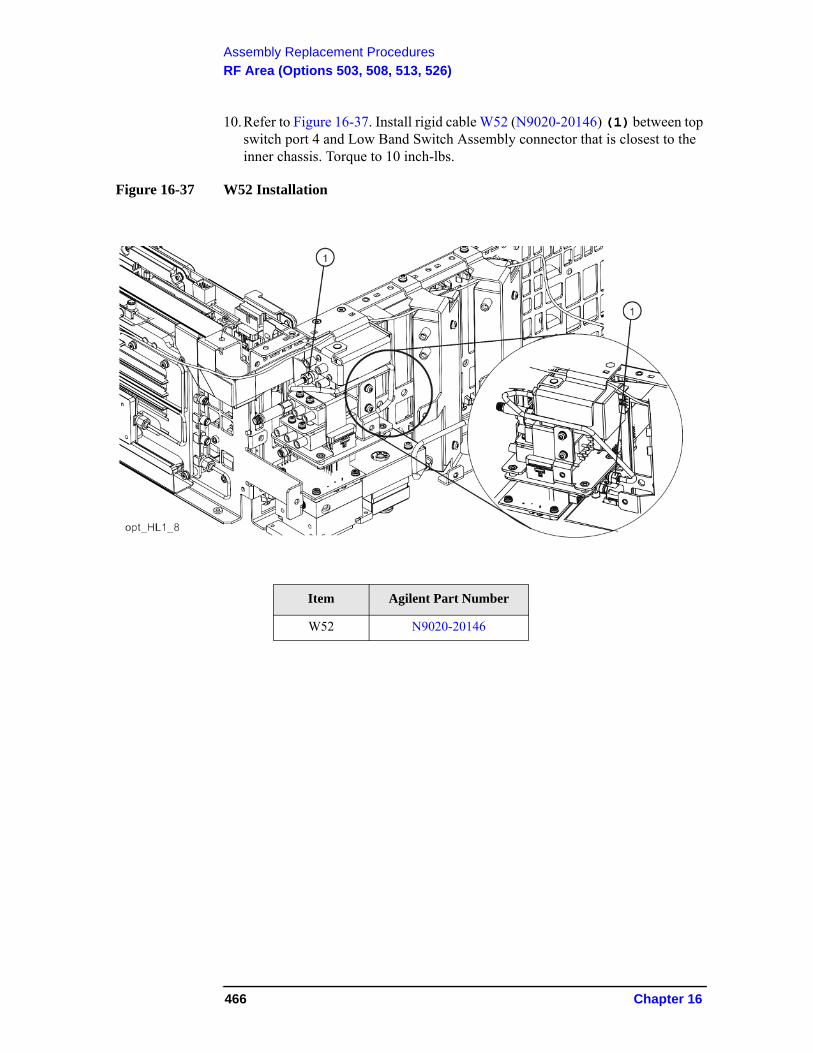
Assembly Replacement Procedures
RF Area (Options 503, 508, 513, 526)
10.Refer to Figure 16-37. Install rigid cable W52 (N9020-20146) (1) between top switch port 4 and Low Band Switch Assembly connector that is closest to the inner chassis. Torque to 10 inch-lbs.
Figure 16-37 W52 Installation
Item Agilent Part Number
W52 N9020-20146
466 Chapter 16
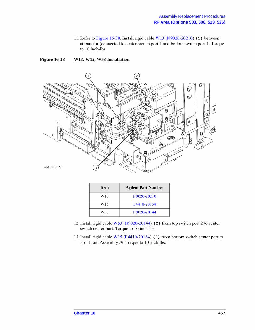
Assembly Replacement Procedures
RF Area (Options 503, 508, 513, 526)
11. Refer to Figure 16-38. Install rigid cable W13 (N9020-20210) (1) between attenuator (connected to center switch port 1 and bottom switch port 1. Torque to 10 inch-lbs.
Figure 16-38 W13, W15, W53 Installation
12. Install rigid cable W53 (N9020-20144) (2) from top switch port 2 to center switch center port. Torque to 10 inch-lbs.
13. Install rigid cable W15 (E4410-20164) (3) from bottom switch center port to Front End Assembly J9. Torque to 10 inch-lbs.
Item Agilent Part Number
W13 N9020-20210
W15 E4410-20164
W53 N9020-20144
Chapter 16 467
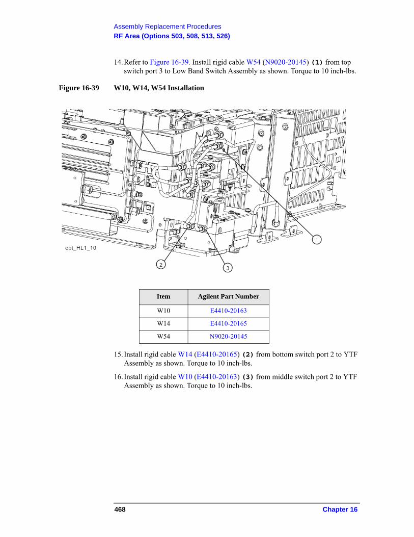
Assembly Replacement Procedures
RF Area (Options 503, 508, 513, 526)
14.Refer to Figure 16-39. Install rigid cable W54 (N9020-20145) (1) from top switch port 3 to Low Band Switch Assembly as shown. Torque to 10 inch-lbs.
Figure 16-39 W10, W14, W54 Installation
15. Install rigid cable W14 (E4410-20165) (2) from bottom switch port 2 to YTF Assembly as shown. Torque to 10 inch-lbs.
16. Install rigid cable W10 (E4410-20163) (3) from middle switch port 2 to YTF Assembly as shown. Torque to 10 inch-lbs.
Item Agilent Part Number
W10 E4410-20163
W14 E4410-20165
W54 N9020-20145
468 Chapter 16
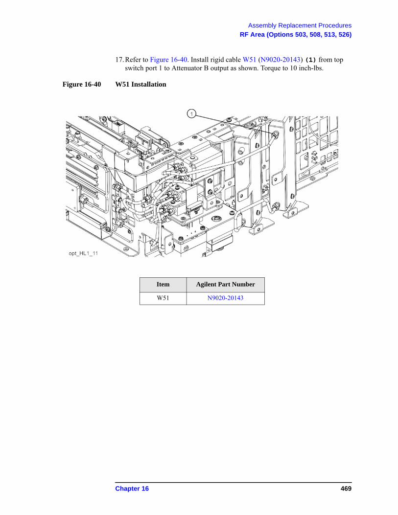
Assembly Replacement Procedures
RF Area (Options 503, 508, 513, 526)
17.Refer to Figure 16-40. Install rigid cable W51 (N9020-20143) (1) from top switch port 1 to Attenuator B output as shown. Torque to 10 inch-lbs.
Figure 16-40 W51 Installation
Item Agilent Part Number
W51 N9020-20143
Chapter 16 469
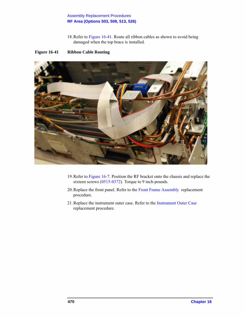
Assembly Replacement Procedures
RF Area (Options 503, 508, 513, 526)
18.Refer to Figure 16-41. Route all ribbon cables as shown to avoid being damaged when the top brace is installed.
Figure 16-41 Ribbon Cable Routing
19.Refer to Figure 16-7. Position the RF bracket onto the chassis and replace the sixteen screws (0515-0372). Torque to 9 inch-pounds.
20.Replace the front panel. Refer to the Front Frame Assembly replacement procedure.
21.Replace the instrument outer case. Refer to the Instrument Outer Case replacement procedure.
470 Chapter 16
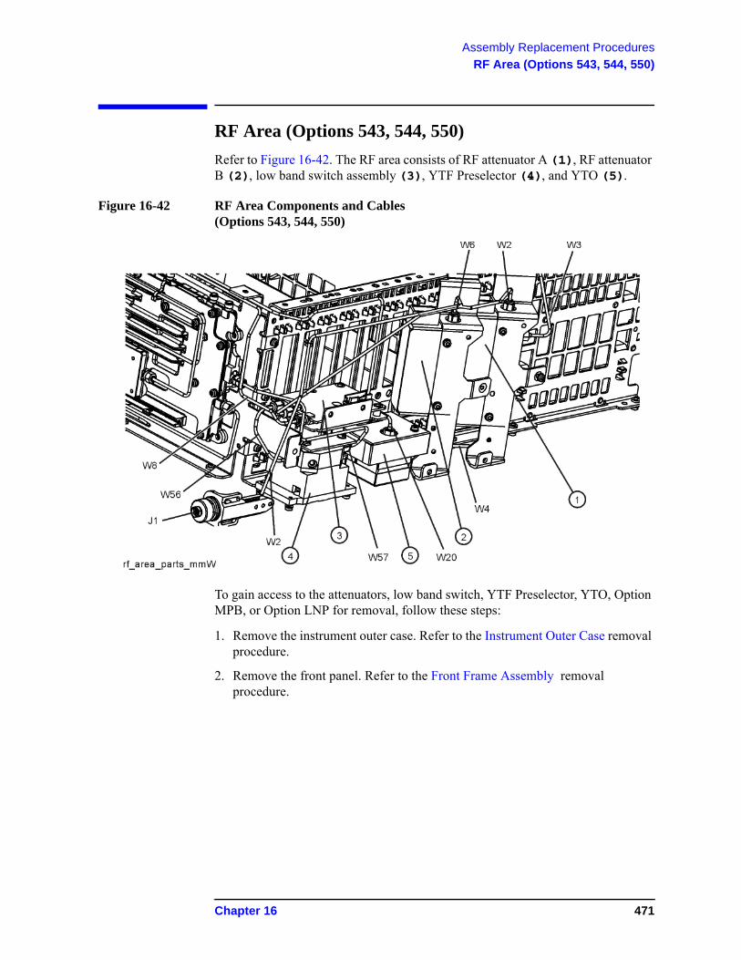
Assembly Replacement Procedures
RF Area (Options 543, 544, 550)
RF Area (Options 543, 544, 550)
Refer to Figure 16-42. The RF area consists of RF attenuator A (1), RF attenuator B (2), low band switch assembly (3), YTF Preselector (4), and YTO (5).
Figure 16-42 RF Area Components and Cables(Options 543, 544, 550)
To gain access to the attenuators, low band switch, YTF Preselector, YTO, Option MPB, or Option LNP for removal, follow these steps:
1. Remove the instrument outer case. Refer to the Instrument Outer Case removal procedure.
2. Remove the front panel. Refer to the Front Frame Assembly removal procedure.
Chapter 16 471
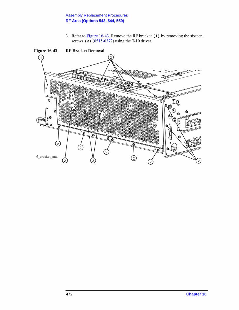
Assembly Replacement Procedures
RF Area (Options 543, 544, 550)
3. Refer to Figure 16-43. Remove the RF bracket (1) by removing the sixteen screws (2) (0515-0372) using the T-10 driver.
Figure 16-43 RF Bracket Removal
472 Chapter 16
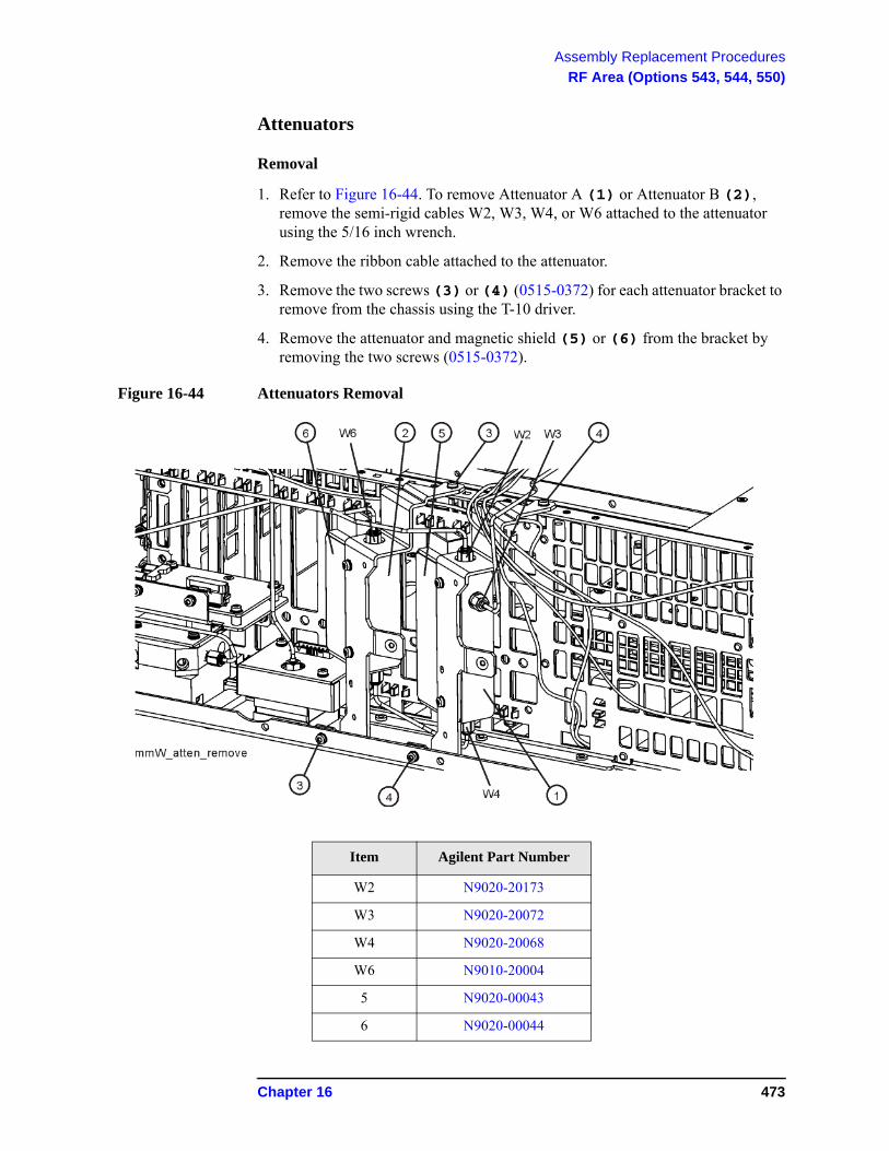
Assembly Replacement Procedures
RF Area (Options 543, 544, 550)
Attenuators
Removal
1. Refer to Figure 16-44. To remove Attenuator A (1) or Attenuator B (2), remove the semi-rigid cables W2, W3, W4, or W6 attached to the attenuator using the 5/16 inch wrench.
2. Remove the ribbon cable attached to the attenuator.
3. Remove the two screws (3) or (4) (0515-0372) for each attenuator bracket to remove from the chassis using the T-10 driver.
4. Remove the attenuator and magnetic shield (5) or (6) from the bracket by removing the two screws (0515-0372).
Figure 16-44 Attenuators Removal
Item Agilent Part Number
W2 N9020-20173
W3 N9020-20072
W4 N9020-20068
W6 N9010-20004
5 N9020-00043
6 N9020-00044
Chapter 16 473
Assembly Replacement Procedures
RF Area (Options 543, 544, 550)
Replacement
1. Refer to Figure 16-44. Position the attenuator and magnetic shield in the bracket so that the attenuator ribbon connector end is “up”.
2. Replace the two screws (0515-0372) that attach the attenuator to the bracket. Torque to 9 inch-pounds.
3. Position the attenuator and bracket into the chassis and attach with the two screws (0515-0372). Torque to 9 inch-pounds.
4. Replace the ribbon cable and semi-rigid cables W2, W3, W4, or W6 to the attenuator. Torque the semi-rigid cables to 10 inch-pounds.
5. Refer to Figure 16-43. Position the RF bracket onto the chassis and replace the sixteen screws (0515-0372). Torque to 9 inch-pounds.
6. Replace the front panel. Refer to the Front Frame Assembly replacement procedure.
7. Replace the instrument outer case. Refer to the Instrument Outer Case replacement procedure.
474 Chapter 16
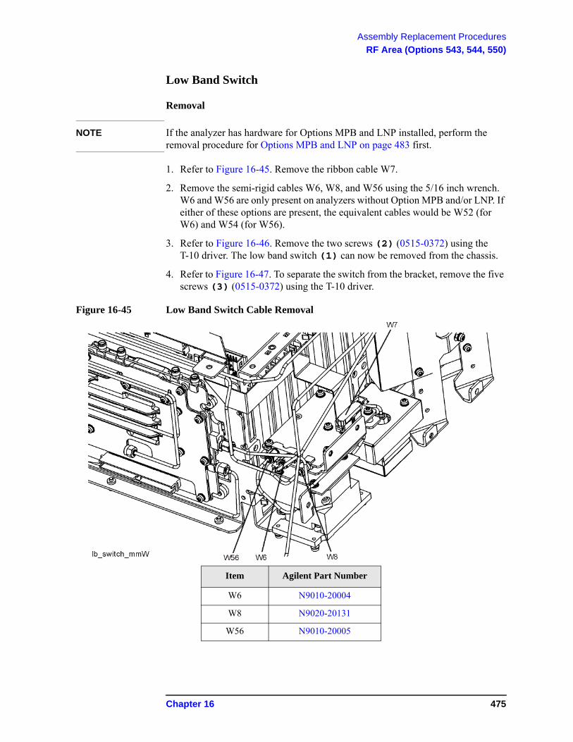
Assembly Replacement Procedures
RF Area (Options 543, 544, 550)
Low Band Switch
Removal
NOTE If the analyzer has hardware for Options MPB and LNP installed, perform the removal procedure for Options MPB and LNP on page 483 first.
1. Refer to Figure 16-45. Remove the ribbon cable W7.
2. Remove the semi-rigid cables W6, W8, and W56 using the 5/16 inch wrench. W6 and W56 are only present on analyzers without Option MPB and/or LNP. If either of these options are present, the equivalent cables would be W52 (for W6) and W54 (for W56).
3. Refer to Figure 16-46. Remove the two screws (2) (0515-0372) using the T-10 driver. The low band switch (1) can now be removed from the chassis.
4. Refer to Figure 16-47. To separate the switch from the bracket, remove the five screws (3) (0515-0372) using the T-10 driver.
Figure 16-45 Low Band Switch Cable Removal
Item Agilent Part Number
W6 N9010-20004
W8 N9020-20131
W56 N9010-20005
Chapter 16 475
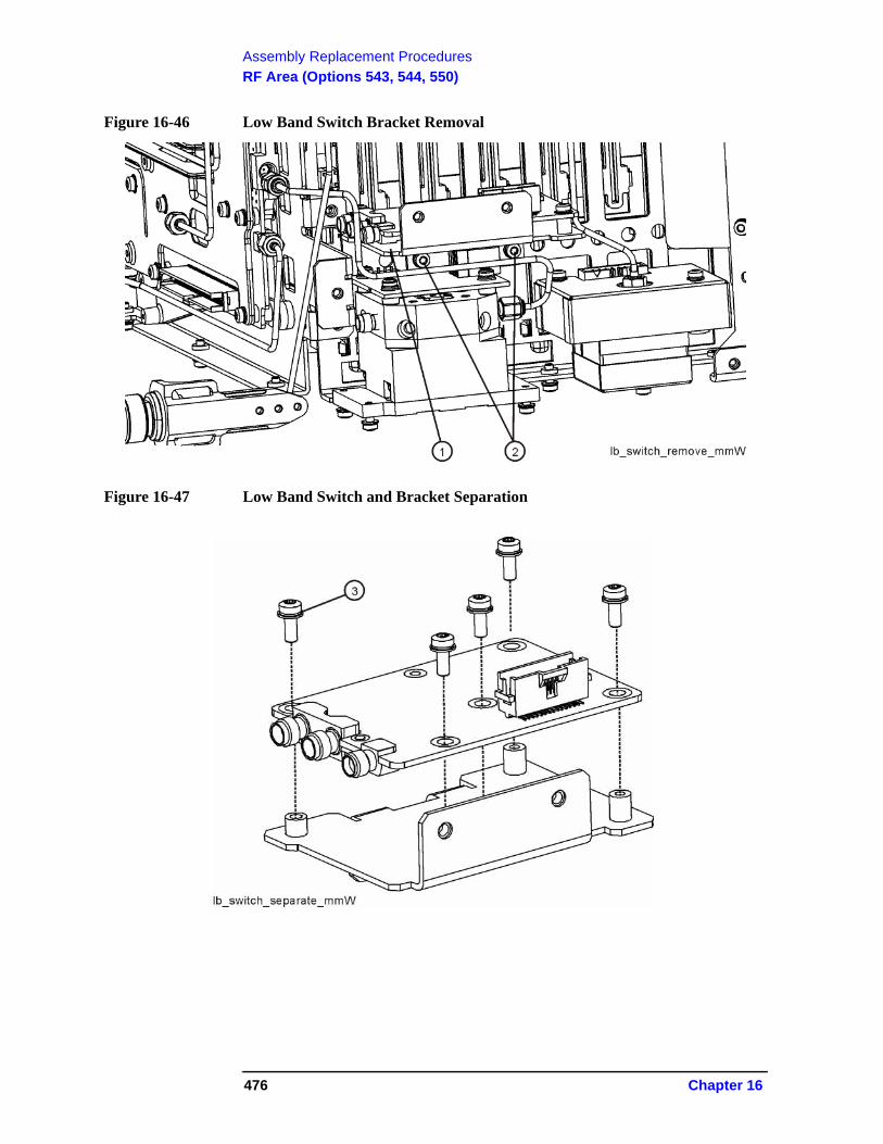
Assembly Replacement Procedures
RF Area (Options 543, 544, 550)
Figure 16-46 Low Band Switch Bracket Removal
Figure 16-47 Low Band Switch and Bracket Separation
476 Chapter 16
Assembly Replacement Procedures
RF Area (Options 543, 544, 550)
Replacement
1. Refer to Figure 16-47. Place the switch onto the bracket and replace the five screws (3) (0515-0372). Torque to 9 inch-pounds.
2. Place the switch/bracket into place into the chassis and replace the two screws (0515-0372). Torque to 9 inch-pounds starting with the screw closest to the front of the instrument.
3. Refer to Figure 16-45. Replace the semi-rigid cables W6, W8, and W56. Torque to 10 inch-pounds.
4. Replace the ribbon cable W7. Ensure locking tabs on the sides of the connector are engaged.
5. Refer to Figure 16-43. Position the RF bracket onto the chassis and replace the sixteen screws (0515-0372). Torque to 9 inch-pounds.
6. Replace the front panel. Refer to the Front Frame Assembly replacement procedure.
7. Replace the instrument outer case. Refer to the Instrument Outer Case replacement procedure.
Chapter 16 477
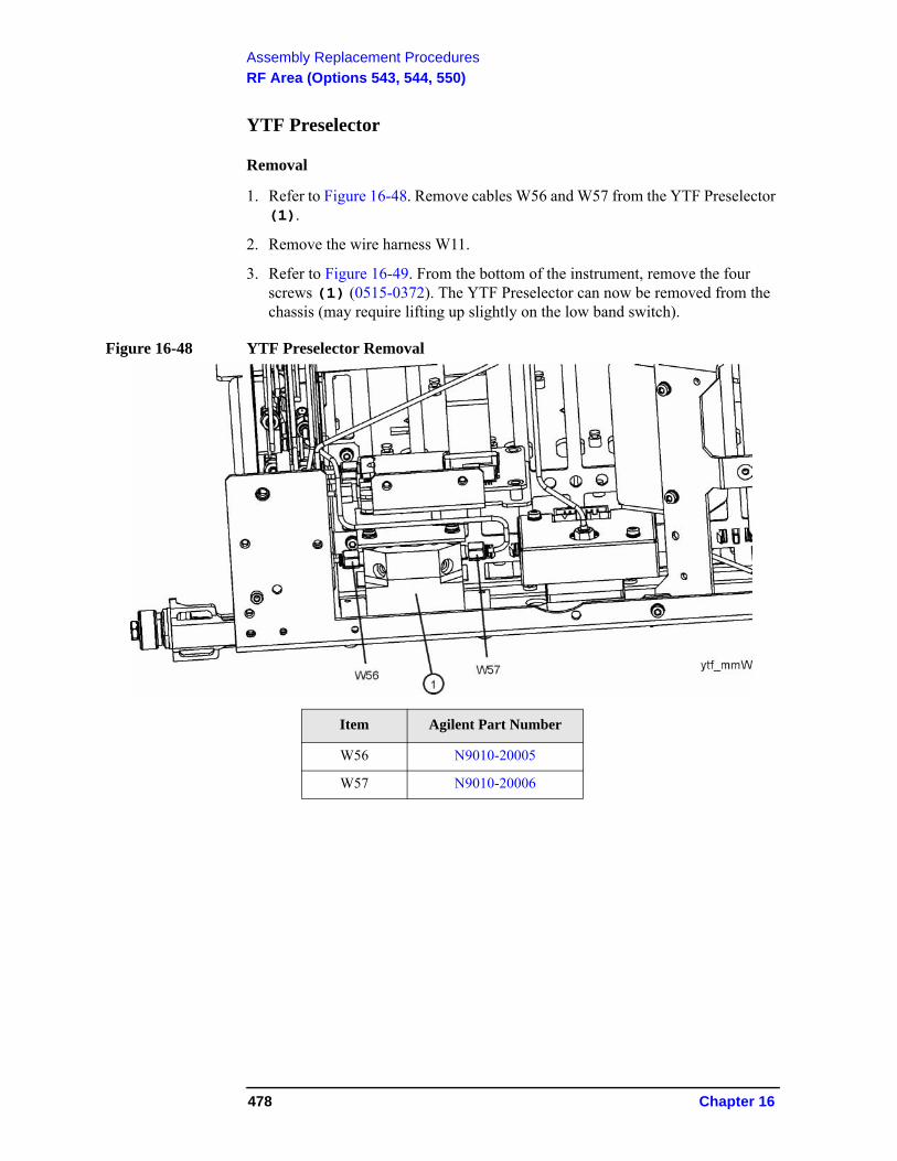
Assembly Replacement Procedures
RF Area (Options 543, 544, 550)
YTF Preselector
Removal
1. Refer to Figure 16-48. Remove cables W56 and W57 from the YTF Preselector (1).
2. Remove the wire harness W11.
3. Refer to Figure 16-49. From the bottom of the instrument, remove the four screws (1) (0515-0372). The YTF Preselector can now be removed from the chassis (may require lifting up slightly on the low band switch).
Figure 16-48 YTF Preselector Removal
Item Agilent Part Number
W56 N9010-20005
W57 N9010-20006
478 Chapter 16
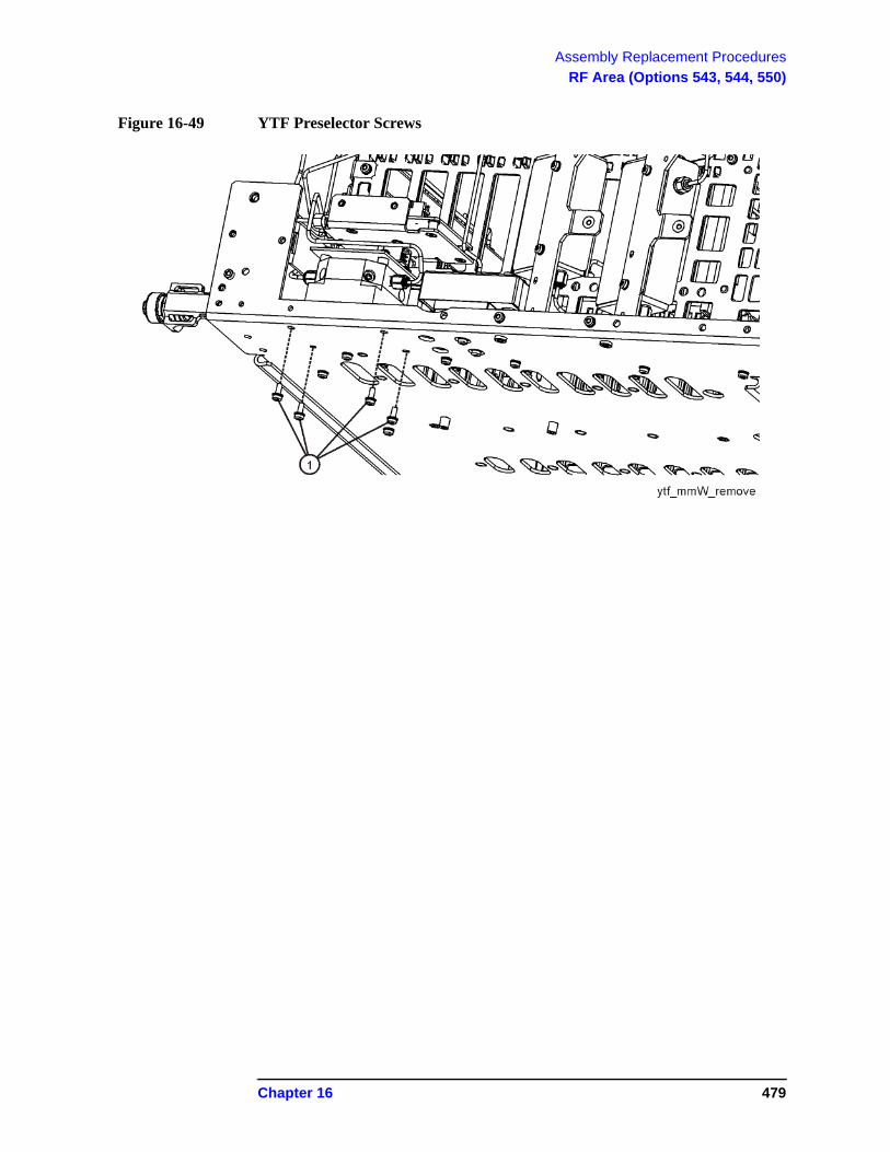
Assembly Replacement Procedures
RF Area (Options 543, 544, 550)
Figure 16-49 YTF Preselector Screws
Chapter 16 479
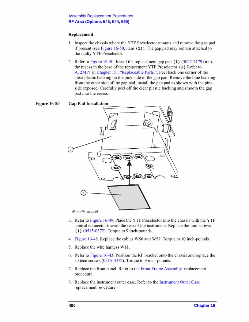
Assembly Replacement Procedures
RF Area (Options 543, 544, 550)
Replacement
1. Inspect the chassis where the YTF Preselector mounts and remove the gap pad if present (see Figure 16-50, item (1)). The gap pad may remain attached to the faulty YTF Preselector.
2. Refer to Figure 16-50. Install the replacement gap pad (1) (5022-7179) into the recess in the base of the replacement YTF Preselector (2) Refer to A12MP1 in Chapter 15 , “Replaceable Parts.”. Peel back one corner of the clear plastic backing on the pink side of the gap pad. Remove the blue backing from the other side of the gap pad. Install the gap pad as shown with the pink side exposed. Carefully peel off the clear plastic backing and smooth the gap pad into the recess.
Figure 16-50 Gap Pad Installation
3. Refer to Figure 16-49. Place the YTF Preselector into the chassis with the YTF control connector toward the rear of the instrument. Replace the four screws (1) (0515-0372). Torque to 9 inch-pounds.
4. Figure 16-48. Replace the cables W56 and W57. Torque to 10 inch-pounds.
5. Replace the wire harness W11.
6. Refer to Figure 16-43. Position the RF bracket onto the chassis and replace the sixteen screws (0515-0372). Torque to 9 inch-pounds.
7. Replace the front panel. Refer to the Front Frame Assembly replacement procedure.
8. Replace the instrument outer case. Refer to the Instrument Outer Case replacement procedure.
480 Chapter 16
Assembly Replacement Procedures
RF Area (Options 543, 544, 550)
YTO
Removal
1. Refer to Figure 16-51. Remove cable W20 from the YTO (1).
2. Remove cable W4.
3. Remove the ribbon cable W23 by pulling forward on the locking latch.
4. Refer to Figure 16-52. From the bottom of the instrument, remove the two screws (1) (0515-0372). The YTO can now be removed from the chassis.
Figure 16-51 YTO Removal
Item Agilent Part Number
W20 N9020-20018
Chapter 16 481
Assembly Replacement Procedures
RF Area (Options 543, 544, 550)
Figure 16-52 YTO Screws
Replacement
1. Refer to Figure 16-52. Place the YTO into the chassis. Replace the two screws (1) (0515-0372). Torque to 9 inch-pounds.
2. Figure 16-51. Replace the cables W20. Torque to 10 inch-pounds.
3. Replace the ribbon cable W23. Ensure the locking latch is engaged.
4. Refer to Figure 16-43. Position the RF bracket onto the chassis and replace the sixteen screws (0515-0372). Torque to 9 inch-pounds.
5. Replace the front panel. Refer to the Front Frame Assembly replacement procedure.
6. Replace the instrument outer case. Refer to the Instrument Outer Case replacement procedure.
482 Chapter 16
Assembly Replacement Procedures
RF Area (Options 543, 544, 550)
Options MPB and LNP
Removal
1. Refer to Figure 16-53. Remove rigid cable W51 (N9020-20171) (1) from top switch port 1 to Attenuator B output.
Figure 16-53 W51 Cable Removal
Chapter 16 483
Assembly Replacement Procedures
RF Area (Options 543, 544, 550)
2. Refer to Figure 16-54 and Figure 16-55. Remove cable W62 (N9020-20130) (3) from bottom switch port 2 to Front End Assembly J9.
3. Remove cable W61 (N9020-20129) (2) from bottom switch port 3 to YTF Assembly.
4. Remove cable W59 (N9020-20151) (1) from top switch port 2 to bottom switch port 1.
Figure 16-54 W62, W61, and W59 Cables Removal
Figure 16-55 Switch Ports
484 Chapter 16
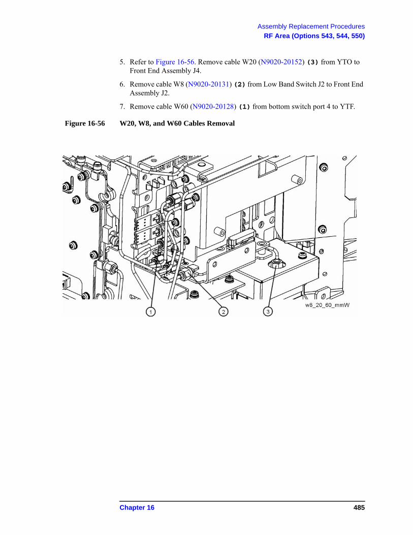
Assembly Replacement Procedures
RF Area (Options 543, 544, 550)
5. Refer to Figure 16-56. Remove cable W20 (N9020-20152) (3) from YTO to Front End Assembly J4.
6. Remove cable W8 (N9020-20131) (2) from Low Band Switch J2 to Front End Assembly J2.
7. Remove cable W60 (N9020-20128) (1) from bottom switch port 4 to YTF.
Figure 16-56 W20, W8, and W60 Cables Removal
Chapter 16 485
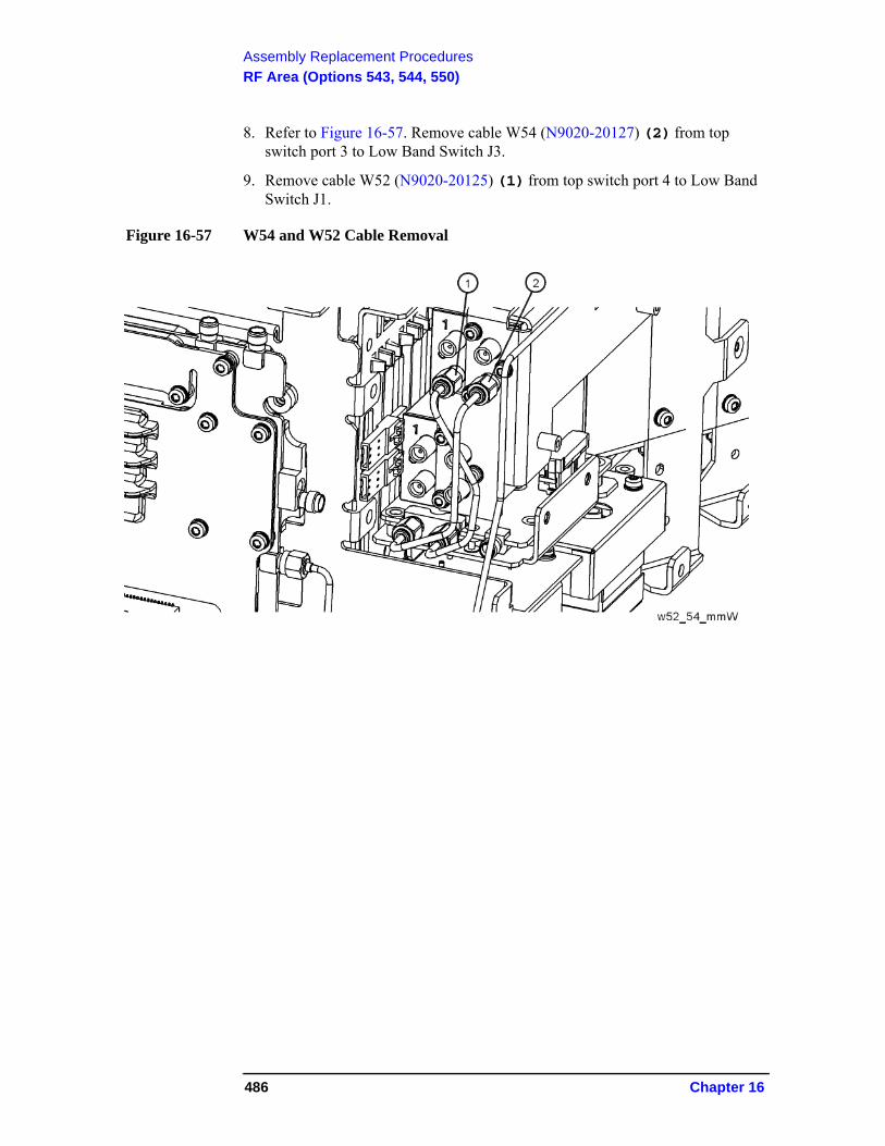
Assembly Replacement Procedures
RF Area (Options 543, 544, 550)
8. Refer to Figure 16-57. Remove cable W54 (N9020-20127) (2) from top switch port 3 to Low Band Switch J3.
9. Remove cable W52 (N9020-20125) (1) from top switch port 4 to Low Band Switch J1.
Figure 16-57 W54 and W52 Cable Removal
486 Chapter 16
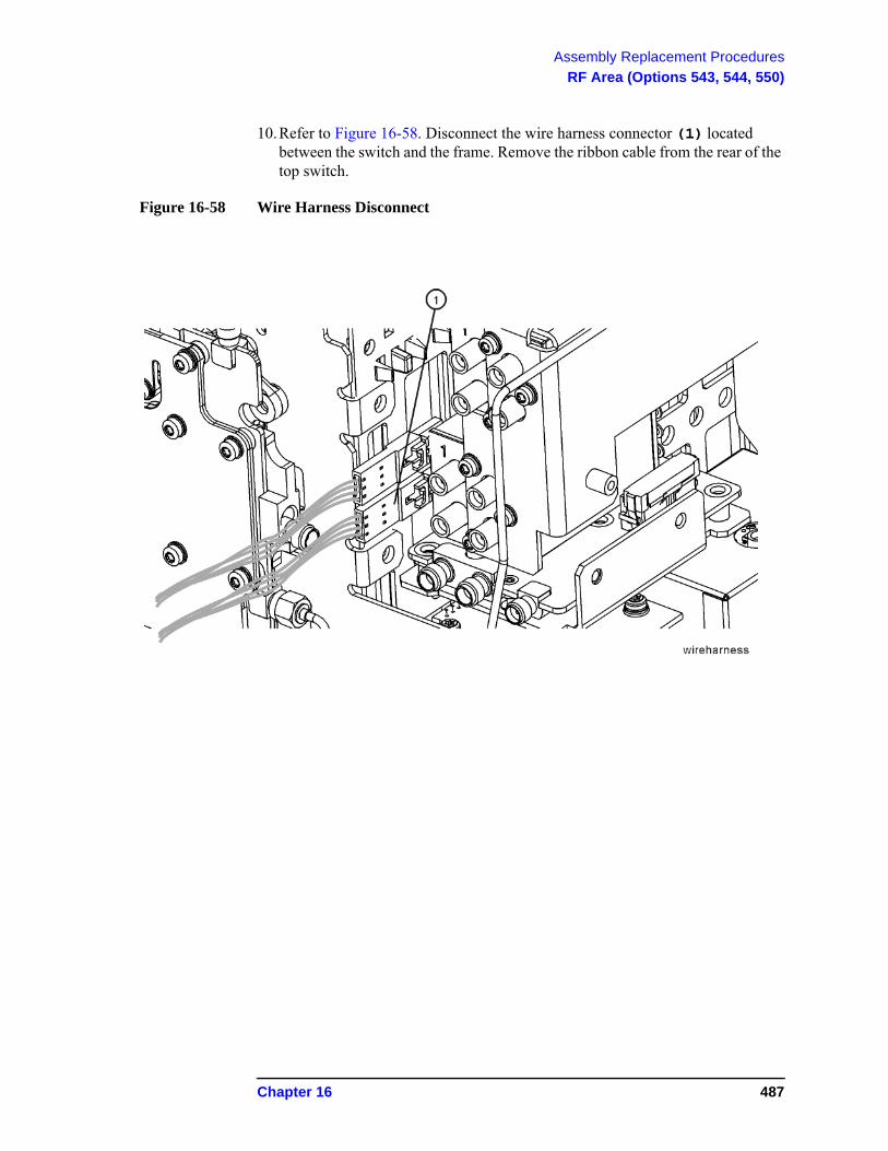
Assembly Replacement Procedures
RF Area (Options 543, 544, 550)
10.Refer to Figure 16-58. Disconnect the wire harness connector (1) located between the switch and the frame. Remove the ribbon cable from the rear of the top switch.
Figure 16-58 Wire Harness Disconnect
Chapter 16 487
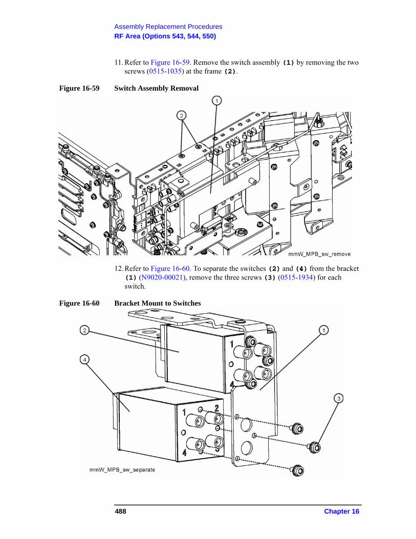
Assembly Replacement Procedures
RF Area (Options 543, 544, 550)
11. Refer to Figure 16-59. Remove the switch assembly (1) by removing the two screws (0515-1035) at the frame (2).
Figure 16-59 Switch Assembly Removal
12.Refer to Figure 16-60. To separate the switches (2) and (4) from the bracket (1) (N9020-00021), remove the three screws (3) (0515-1934) for each switch.
Figure 16-60 Bracket Mount to Switches
488 Chapter 16
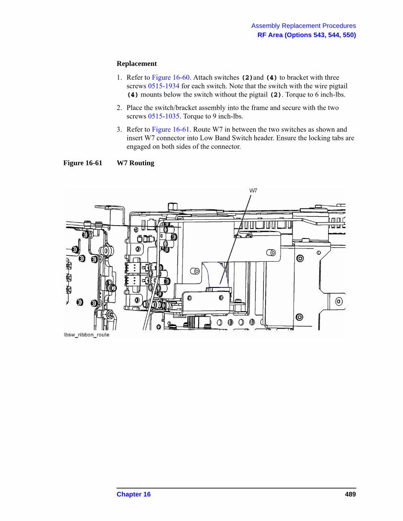
Assembly Replacement Procedures
RF Area (Options 543, 544, 550)
Replacement
1. Refer to Figure 16-60. Attach switches (2)and (4) to bracket with three screws 0515-1934 for each switch. Note that the switch with the wire pigtail (4) mounts below the switch without the pigtail (2). Torque to 6 inch-lbs.
2. Place the switch/bracket assembly into the frame and secure with the two screws 0515-1035. Torque to 9 inch-lbs.
3. Refer to Figure 16-61. Route W7 in between the two switches as shown and insert W7 connector into Low Band Switch header. Ensure the locking tabs are engaged on both sides of the connector.
Figure 16-61 W7 Routing
Chapter 16 489
Assembly Replacement Procedures
RF Area (Options 543, 544, 550)
4. Reconnect the wire harness connector. Once connected, position the connections along side the switches as shown in Figure 16-58. Plug in the ribbon cable to the rear of the top switch.
5. Refer to Figure 16-57. Replace cable W52 (N9020-20125) (1) between top switch port 4 to Low Band Switch J1. Torque to 10 inch-pounds.
6. Replace cable W54 (N9020-20127) (2) between top switch port 3 to Low Band Switch J3. Torque to 10 inch-pounds.
7. Refer to Figure 16-56. Replace cable W60 (N9020-20128) (1) between bottom switch port 4 to YTF. Torque to 10 inch-pounds.
8. Replace cable W8 (N9020-20131) (2) between Low Band Switch J2 to Front End Assembly J2. Torque to 10 inch-pounds.
9. Replace cable W20 (N9020-20152) (3) between YTO to Front End Assembly J4. Torque to 10 inch-pounds.
10.Replace cable W59 (N9020-20151) (1) between top switch port 2 to bottom switch port 1. Torque to 10 inch-pounds.
11. Replace cable W61 (N9020-20129) (2) between bottom switch port 3 to YTF Assembly. Torque to 10 inch-pounds.
12.Refer to Figure 16-54. Replace cable W62 (N9020-20130) (3) between bottom switch port 2 to Front End Assembly J9. Torque to 10 inch-pounds.
13.Refer to Figure 16-53. Replace rigid cable W51 (N9020-20171) (1) between top switch port 1 to Attenuator B output. Torque to 10 inch-pounds.
14.Route all ribbon cables to avoid being damaged when the top brace is installed.
15.Refer to Figure 16-43. Position the RF bracket onto the chassis and replace the sixteen screws (0515-0372). Torque to 9 inch-pounds.
16.Replace the front panel. Refer to the Front Frame Assembly replacement procedure.
17.Replace the instrument outer case. Refer to the Instrument Outer Case replacement procedure.
490 Chapter 16
Assembly Replacement Procedures
RF Front End Assembly
RF Front End Assembly
Removal
1. Remove the instrument outer case. Refer to the Instrument Outer Case removal procedure.
2. Remove the instrument top brace. Refer to the Top Brace and Power Supply Bracket removal procedure.
3. Remove the front panel. Refer to the Front Frame Assembly removal procedure.
4. Refer to Figure 16-62 and Figure 16-63. Using the 5/16 inch wrench, remove the cables attached to A13A1J1, A13A1J2, A13A1J4, A13A1J5, A13A1J6, A13A1J7, A13A1J9 on the RF Front End Assembly. If the analyzer has Option EXM, remove the cables attached to A13A1J8 and A13A1J13 also.
5. Remove the W22 and W28 ribbon cables from Front End Controller board connectors J102 and J1300. The ribbon cables then can be removed from the Front End Assembly connectors A13A1J12 and A13A2J1 once it is out of the instrument.
6. Remove the six screws (1) (0515-0372) using the T-10 driver. The RF Front End Assembly can now be removed from the chassis.
Chapter 16 491
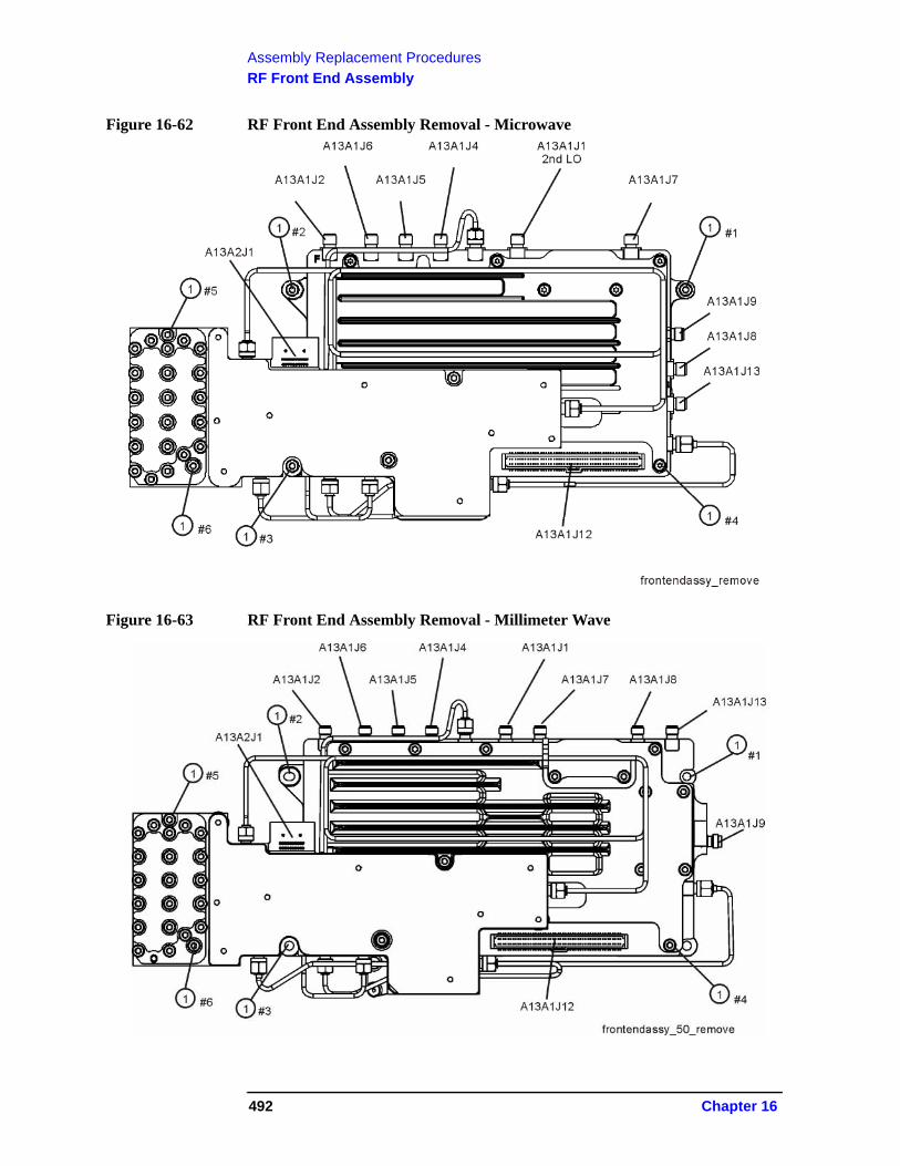
Assembly Replacement Procedures
RF Front End Assembly
Figure 16-62 RF Front End Assembly Removal - Microwave
Figure 16-63 RF Front End Assembly Removal - Millimeter Wave
492 Chapter 16
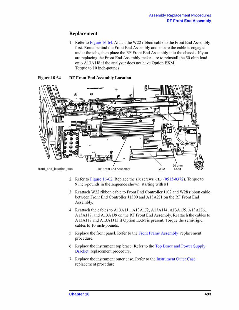
Assembly Replacement Procedures
RF Front End Assembly
Replacement
1. Refer to Figure 16-64. Attach the W22 ribbon cable to the Front End Assembly first. Route behind the Front End Assembly and ensure the cable is engaged under the tabs, then place the RF Front End Assembly into the chassis. If you are replacing the Front End Assembly make sure to reinstall the 50 ohm load onto A13A1J8 if the analyzer does not have Option EXM. Torque to 10 inch-pounds.
Figure 16-64 RF Front End Assembly Location
2. Refer to Figure 16-62. Replace the six screws (1) (0515-0372). Torque to 9 inch-pounds in the sequence shown, starting with #1.
3. Reattach W22 ribbon cable to Front End Controller J102 and W28 ribbon cable between Front End Controller J1300 and A13A2J1 on the RF Front End Assembly.
4. Reattach the cables to A13A1J1, A13A1J2, A13A1J4, A13A1J5, A13A1J6, A13A1J7, and A13A1J9 on the RF Front End Assembly. Reattach the cables to A13A1J8 and A13A1J13 if Option EXM is present. Torque the semi-rigid cables to 10 inch-pounds.
5. Replace the front panel. Refer to the Front Frame Assembly replacement procedure.
6. Replace the instrument top brace. Refer to the Top Brace and Power Supply Bracket replacement procedure.
7. Replace the instrument outer case. Refer to the Instrument Outer Case replacement procedure.
Chapter 16 493
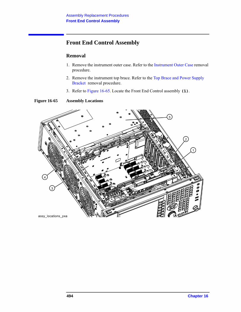
Assembly Replacement Procedures
Front End Control Assembly
Front End Control Assembly
Removal
1. Remove the instrument outer case. Refer to the Instrument Outer Case removal procedure.
2. Remove the instrument top brace. Refer to the Top Brace and Power Supply Bracket removal procedure.
3. Refer to Figure 16-65. Locate the Front End Control assembly (1).
Figure 16-65 Assembly Locations
494 Chapter 16
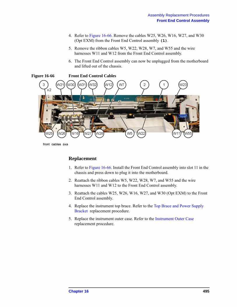
Assembly Replacement Procedures
Front End Control Assembly
4. Refer to Figure 16-66. Remove the cables W25, W26, W16, W27, and W30 (Opt EXM) from the Front End Control assembly (1).
5. Remove the ribbon cables W5, W22, W28, W7, and W55 and the wire harnesses W11 and W12 from the Front End Control assembly.
6. The Front End Control assembly can now be unplugged from the motherboard and lifted out of the chassis.
Figure 16-66 Front End Control Cables
Replacement
1. Refer to Figure 16-66. Install the Front End Control assembly into slot 11 in the chassis and press down to plug it into the motherboard.
2. Reattach the ribbon cables W5, W22, W28, W7, and W55 and the wire harnesses W11 and W12 to the Front End Control assembly.
3. Reattach the cables W25, W26, W16, W27, and W30 (Opt EXM) to the Front End Control assembly.
4. Replace the instrument top brace. Refer to the Top Brace and Power Supply Bracket replacement procedure.
5. Replace the instrument outer case. Refer to the Instrument Outer Case replacement procedure.
Chapter 16 495
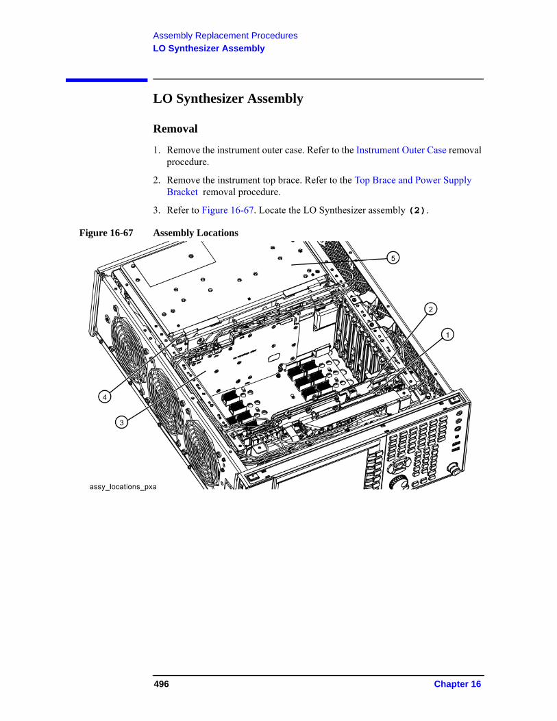
Assembly Replacement Procedures
LO Synthesizer Assembly
LO Synthesizer Assembly
Removal
1. Remove the instrument outer case. Refer to the Instrument Outer Case removal procedure.
2. Remove the instrument top brace. Refer to the Top Brace and Power Supply Bracket removal procedure.
3. Refer to Figure 16-67. Locate the LO Synthesizer assembly (2).
Figure 16-67 Assembly Locations
496 Chapter 16
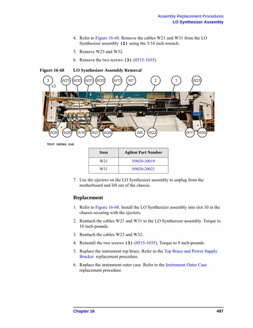
Assembly Replacement Procedures
LO Synthesizer Assembly
4. Refer to Figure 16-68. Remove the cables W21 and W31 from the LO Synthesizer assembly (2) using the 5/16 inch wrench.
5. Remove W23 and W32.
6. Remove the two screws (3) (0515-1035).
Figure 16-68 LO Synthesizer Assembly Removal
7. Use the ejectors on the LO Synthesizer assembly to unplug from the motherboard and lift out of the chassis.
Replacement
1. Refer to Figure 16-68. Install the LO Synthesizer assembly into slot 10 in the chassis securing with the ejectors.
2. Reattach the cables W21 and W31 to the LO Synthesizer assembly. Torque to 10 inch-pounds.
3. Reattach the cables W23 and W32.
4. Reinstall the two screws (3) (0515-1035). Torque to 9 inch-pounds.
5. Replace the instrument top brace. Refer to the Top Brace and Power Supply Bracket replacement procedure.
6. Replace the instrument outer case. Refer to the Instrument Outer Case replacement procedure.
Item Agilent Part Number
W21 N9020-20019
W31 N9020-20021
Chapter 16 497
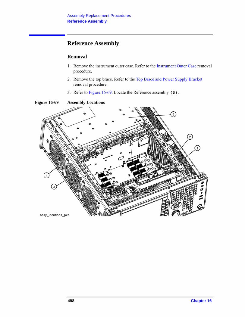
Assembly Replacement Procedures
Reference Assembly
Reference Assembly
Removal
1. Remove the instrument outer case. Refer to the Instrument Outer Case removal procedure.
2. Remove the top brace. Refer to the Top Brace and Power Supply Bracket removal procedure.
3. Refer to Figure 16-69. Locate the Reference assembly (3).
Figure 16-69 Assembly Locations
498 Chapter 16
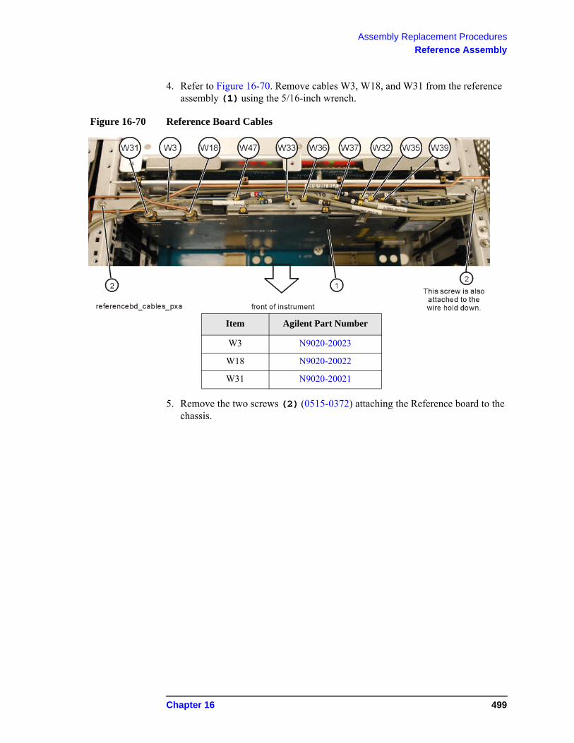
Assembly Replacement Procedures
Reference Assembly
4. Refer to Figure 16-70. Remove cables W3, W18, and W31 from the reference assembly (1) using the 5/16-inch wrench.
Figure 16-70 Reference Board Cables
5. Remove the two screws (2) (0515-0372) attaching the Reference board to the chassis.
Item Agilent Part Number
W3 N9020-20023
W18 N9020-20022
W31 N9020-20021
Chapter 16 499
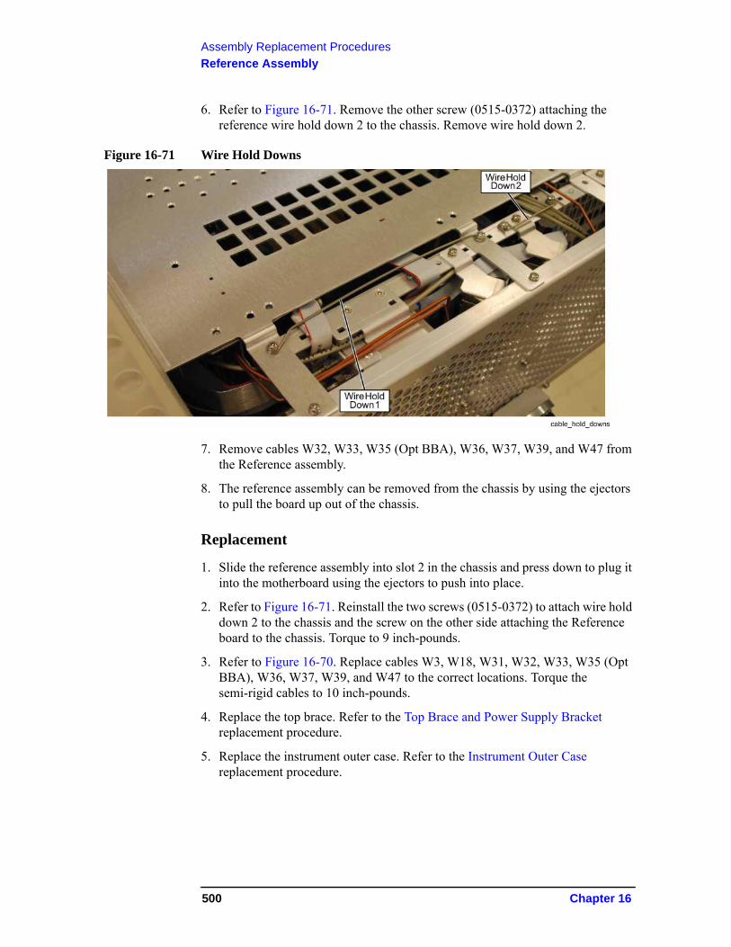
Assembly Replacement Procedures
Reference Assembly
6. Refer to Figure 16-71. Remove the other screw (0515-0372) attaching the reference wire hold down 2 to the chassis. Remove wire hold down 2.
Figure 16-71 Wire Hold Downs
7. Remove cables W32, W33, W35 (Opt BBA), W36, W37, W39, and W47 from the Reference assembly.
8. The reference assembly can be removed from the chassis by using the ejectors to pull the board up out of the chassis.
Replacement
1. Slide the reference assembly into slot 2 in the chassis and press down to plug it into the motherboard using the ejectors to push into place.
2. Refer to Figure 16-71. Reinstall the two screws (0515-0372) to attach wire hold down 2 to the chassis and the screw on the other side attaching the Reference board to the chassis. Torque to 9 inch-pounds.
3. Refer to Figure 16-70. Replace cables W3, W18, W31, W32, W33, W35 (Opt BBA), W36, W37, W39, and W47 to the correct locations. Torque the semi-rigid cables to 10 inch-pounds.
4. Replace the top brace. Refer to the Top Brace and Power Supply Bracket replacement procedure.
5. Replace the instrument outer case. Refer to the Instrument Outer Case replacement procedure.
500 Chapter 16
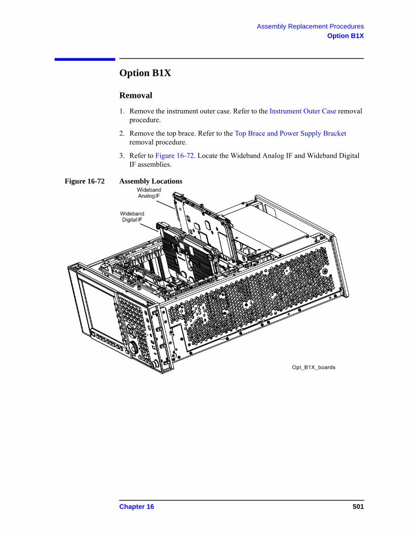
Assembly Replacement Procedures
Option B1X
Option B1X
Removal
1. Remove the instrument outer case. Refer to the Instrument Outer Case removal procedure.
2. Remove the top brace. Refer to the Top Brace and Power Supply Bracket removal procedure.
3. Refer to Figure 16-72. Locate the Wideband Analog IF and Wideband Digital IF assemblies.
Figure 16-72 Assembly Locations
Chapter 16 501
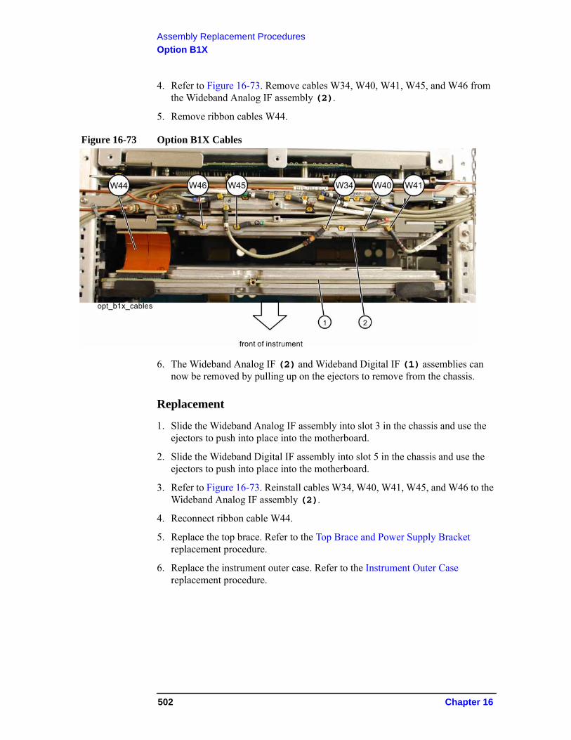
Assembly Replacement Procedures
Option B1X
4. Refer to Figure 16-73. Remove cables W34, W40, W41, W45, and W46 from the Wideband Analog IF assembly (2).
5. Remove ribbon cables W44.
Figure 16-73 Option B1X Cables
6. The Wideband Analog IF (2) and Wideband Digital IF (1) assemblies can now be removed by pulling up on the ejectors to remove from the chassis.
Replacement
1. Slide the Wideband Analog IF assembly into slot 3 in the chassis and use the ejectors to push into place into the motherboard.
2. Slide the Wideband Digital IF assembly into slot 5 in the chassis and use the ejectors to push into place into the motherboard.
3. Refer to Figure 16-73. Reinstall cables W34, W40, W41, W45, and W46 to the Wideband Analog IF assembly (2).
4. Reconnect ribbon cable W44.
5. Replace the top brace. Refer to the Top Brace and Power Supply Bracket replacement procedure.
6. Replace the instrument outer case. Refer to the Instrument Outer Case replacement procedure.
502 Chapter 16
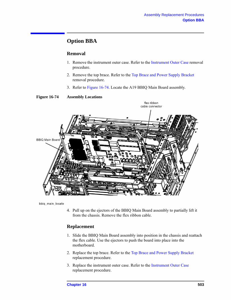
Assembly Replacement Procedures
Option BBA
Option BBA
Removal
1. Remove the instrument outer case. Refer to the Instrument Outer Case removal procedure.
2. Remove the top brace. Refer to the Top Brace and Power Supply Bracket removal procedure.
3. Refer to Figure 16-74. Locate the A19 BBIQ Main Board assembly.
Figure 16-74 Assembly Locations
4. Pull up on the ejectors of the BBIQ Main Board assembly to partially lift it from the chassis. Remove the flex ribbon cable.
Replacement
1. Slide the BBIQ Main Board assembly into position in the chassis and reattach the flex cable. Use the ejectors to push the board into place into the motherboard.
2. Replace the top brace. Refer to the Top Brace and Power Supply Bracket replacement procedure.
3. Replace the instrument outer case. Refer to the Instrument Outer Case replacement procedure.
Chapter 16 503
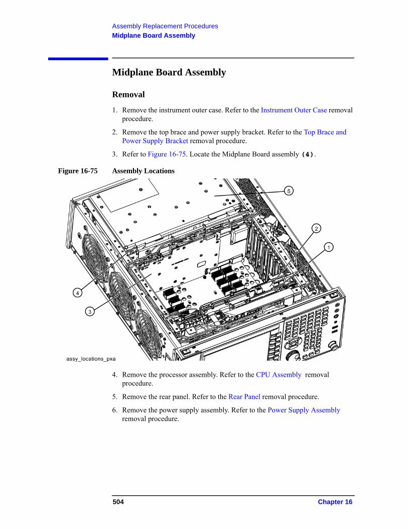
Assembly Replacement Procedures
Midplane Board Assembly
Midplane Board Assembly
Removal
1. Remove the instrument outer case. Refer to the Instrument Outer Case removal procedure.
2. Remove the top brace and power supply bracket. Refer to the Top Brace and Power Supply Bracket removal procedure.
3. Refer to Figure 16-75. Locate the Midplane Board assembly (4).
Figure 16-75 Assembly Locations
4. Remove the processor assembly. Refer to the CPU Assembly removal procedure.
5. Remove the rear panel. Refer to the Rear Panel removal procedure.
6. Remove the power supply assembly. Refer to the Power Supply Assembly removal procedure.
504 Chapter 16
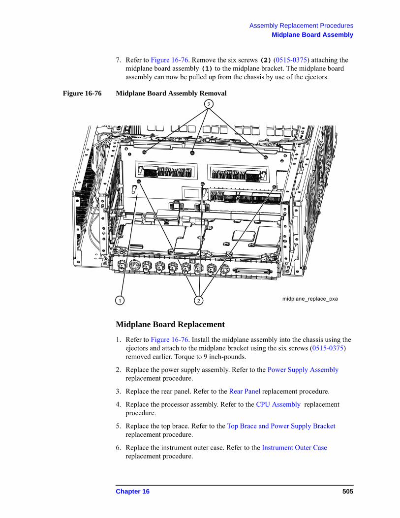
Assembly Replacement Procedures
Midplane Board Assembly
7. Refer to Figure 16-76. Remove the six screws (2) (0515-0375) attaching the midplane board assembly (1) to the midplane bracket. The midplane board assembly can now be pulled up from the chassis by use of the ejectors.
Figure 16-76 Midplane Board Assembly Removal
Midplane Board Replacement
1. Refer to Figure 16-76. Install the midplane assembly into the chassis using the ejectors and attach to the midplane bracket using the six screws (0515-0375) removed earlier. Torque to 9 inch-pounds.
2. Replace the power supply assembly. Refer to the Power Supply Assembly replacement procedure.
3. Replace the rear panel. Refer to the Rear Panel replacement procedure.
4. Replace the processor assembly. Refer to the CPU Assembly replacement procedure.
5. Replace the top brace. Refer to the Top Brace and Power Supply Bracket replacement procedure.
6. Replace the instrument outer case. Refer to the Instrument Outer Case replacement procedure.
Chapter 16 505
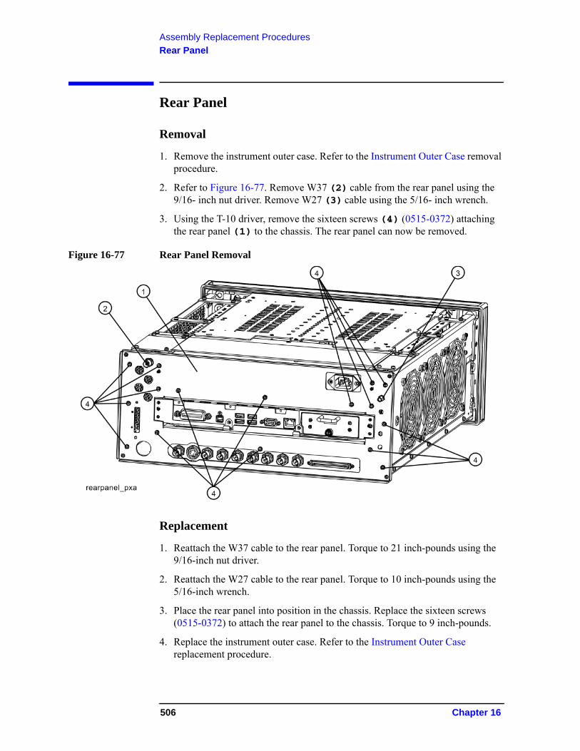
Assembly Replacement Procedures
Rear Panel
Rear Panel
Removal
1. Remove the instrument outer case. Refer to the Instrument Outer Case removal procedure.
2. Refer to Figure 16-77. Remove W37 (2) cable from the rear panel using the 9/16- inch nut driver. Remove W27 (3) cable using the 5/16- inch wrench.
3. Using the T-10 driver, remove the sixteen screws (4) (0515-0372) attaching the rear panel (1) to the chassis. The rear panel can now be removed.
Figure 16-77 Rear Panel Removal
Replacement
1. Reattach the W37 cable to the rear panel. Torque to 21 inch-pounds using the 9/16-inch nut driver.
2. Reattach the W27 cable to the rear panel. Torque to 10 inch-pounds using the 5/16-inch wrench.
3. Place the rear panel into position in the chassis. Replace the sixteen screws (0515-0372) to attach the rear panel to the chassis. Torque to 9 inch-pounds.
4. Replace the instrument outer case. Refer to the Instrument Outer Case replacement procedure.
506 Chapter 16
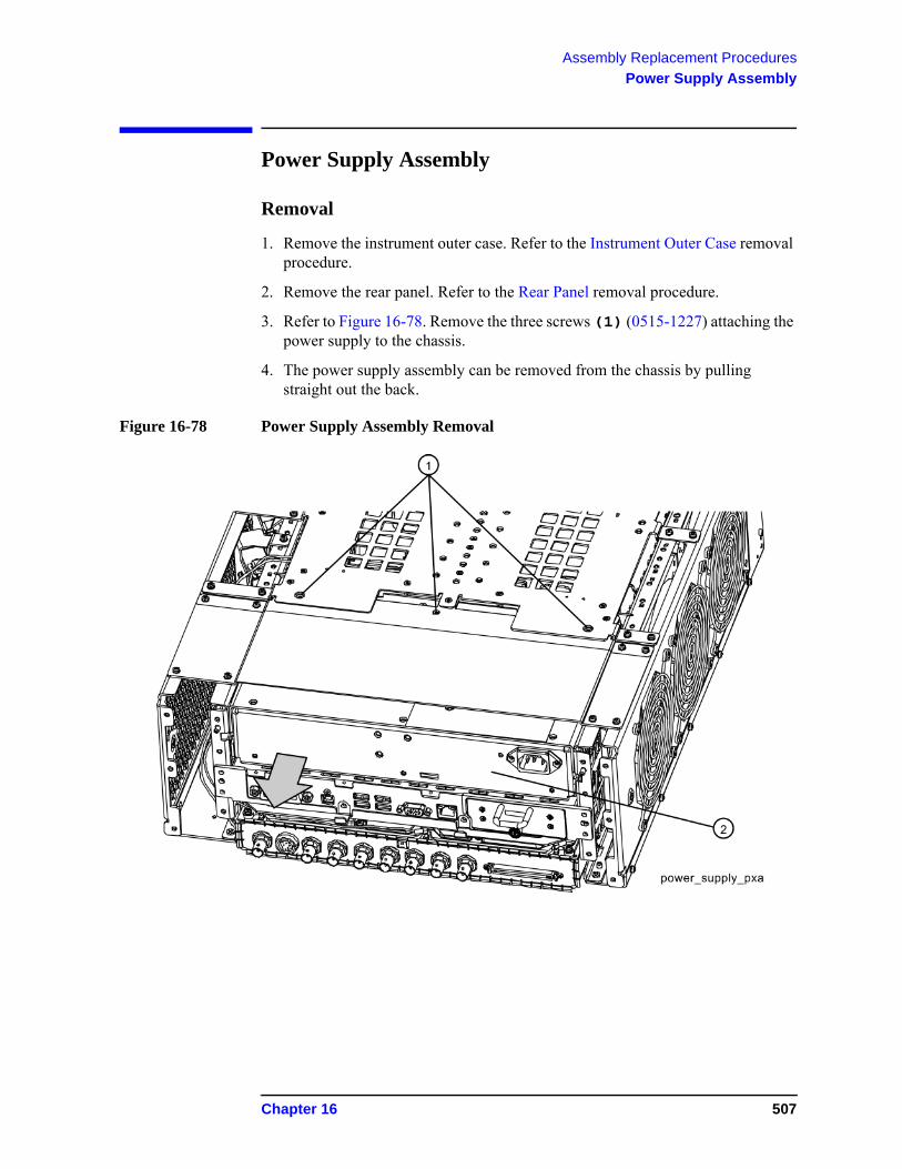
Assembly Replacement Procedures
Power Supply Assembly
Power Supply Assembly
Removal
1. Remove the instrument outer case. Refer to the Instrument Outer Case removal procedure.
2. Remove the rear panel. Refer to the Rear Panel removal procedure.
3. Refer to Figure 16-78. Remove the three screws (1) (0515-1227) attaching the power supply to the chassis.
4. The power supply assembly can be removed from the chassis by pulling straight out the back.
Figure 16-78 Power Supply Assembly Removal
Chapter 16 507
Assembly Replacement Procedures
Power Supply Assembly
Replacement
1. Slide the power supply assembly into the slot at the rear of the instrument and push on the assembly to mate the connectors to the midplane assembly.
2. Refer to Figure 16-78. Replace the three screws (1) (0515-1227) through the power supply bracket and into the power supply. Torque to 9 inch-pounds.
3. Replace the rear panel. Refer to the Rear Panel replacement procedure.
4. Replace the instrument outer case. Refer to the Instrument Outer Case replacement procedure.
508 Chapter 16
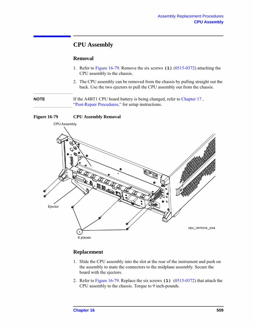
Assembly Replacement Procedures
CPU Assembly
CPU Assembly
Removal
1. Refer to Figure 16-79. Remove the six screws (1) (0515-0372) attaching the CPU assembly to the chassis.
2. The CPU assembly can be removed from the chassis by pulling straight out the back. Use the two ejectors to pull the CPU assembly out from the chassis.
NOTE If the A4BT1 CPU board battery is being changed, refer to Chapter 17 , “Post-Repair Procedures,” for setup instructions.
Figure 16-79 CPU Assembly Removal
Replacement
1. Slide the CPU assembly into the slot at the rear of the instrument and push on the assembly to mate the connectors to the midplane assembly. Secure the board with the ejectors.
2. Refer to Figure 16-79. Replace the six screws (1) (0515-0372) that attach the CPU assembly to the chassis. Torque to 9 inch-pounds.
Chapter 16 509
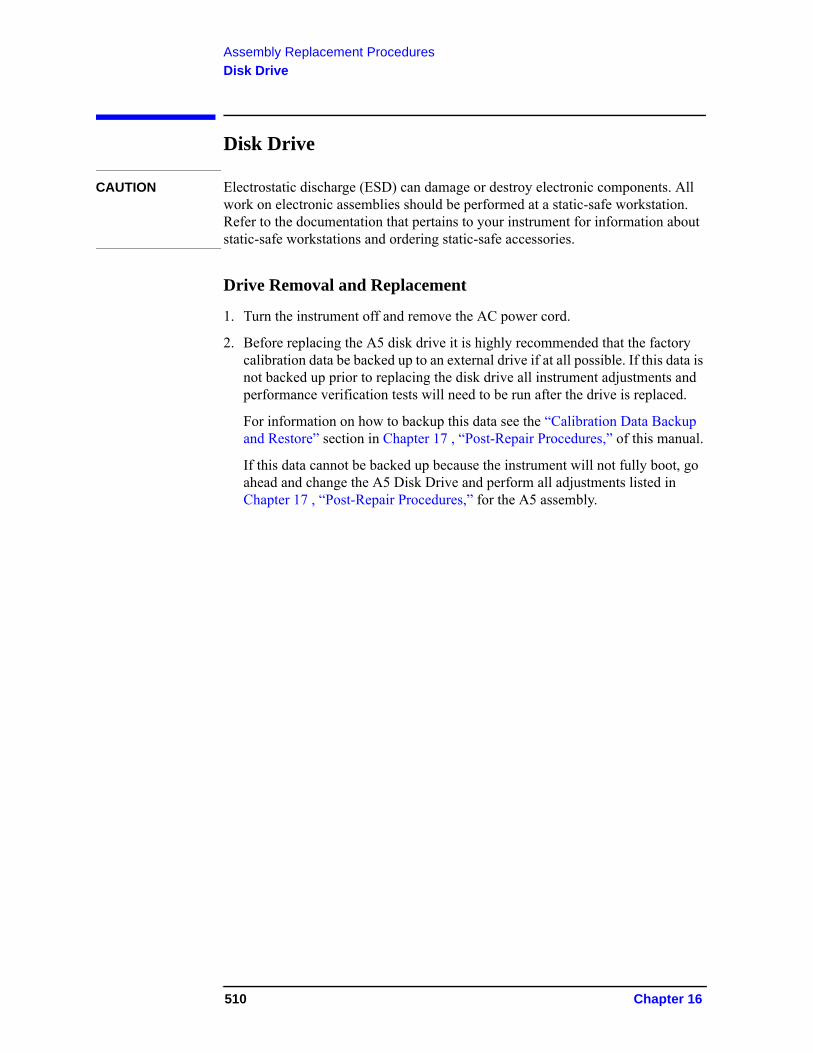
Assembly Replacement Procedures
Disk Drive
Disk Drive
CAUTION Electrostatic discharge (ESD) can damage or destroy electronic components. All work on electronic assemblies should be performed at a static-safe workstation. Refer to the documentation that pertains to your instrument for information about static-safe workstations and ordering static-safe accessories.
Drive Removal and Replacement
1. Turn the instrument off and remove the AC power cord.
2. Before replacing the A5 disk drive it is highly recommended that the factory calibration data be backed up to an external drive if at all possible. If this data is not backed up prior to replacing the disk drive all instrument adjustments and performance verification tests will need to be run after the drive is replaced.
For information on how to backup this data see the “Calibration Data Backup and Restore” section in Chapter 17 , “Post-Repair Procedures,” of this manual.
If this data cannot be backed up because the instrument will not fully boot, go ahead and change the A5 Disk Drive and perform all adjustments listed in Chapter 17 , “Post-Repair Procedures,” for the A5 assembly.
510 Chapter 16
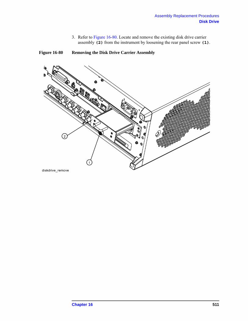
Assembly Replacement Procedures
Disk Drive
3. Refer to Figure 16-80. Locate and remove the existing disk drive carrier assembly (2) from the instrument by loosening the rear panel screw (1).
Figure 16-80 Removing the Disk Drive Carrier Assembly
Chapter 16 511
Assembly Replacement Procedures
Disk Drive
4. Refer to Figure 16-81. Remove the 4 machine screws (1) (0515-0372) from the disk drive carrier assembly that secure the drive (2).
Figure 16-81 Disk Drive Screws
512 Chapter 16
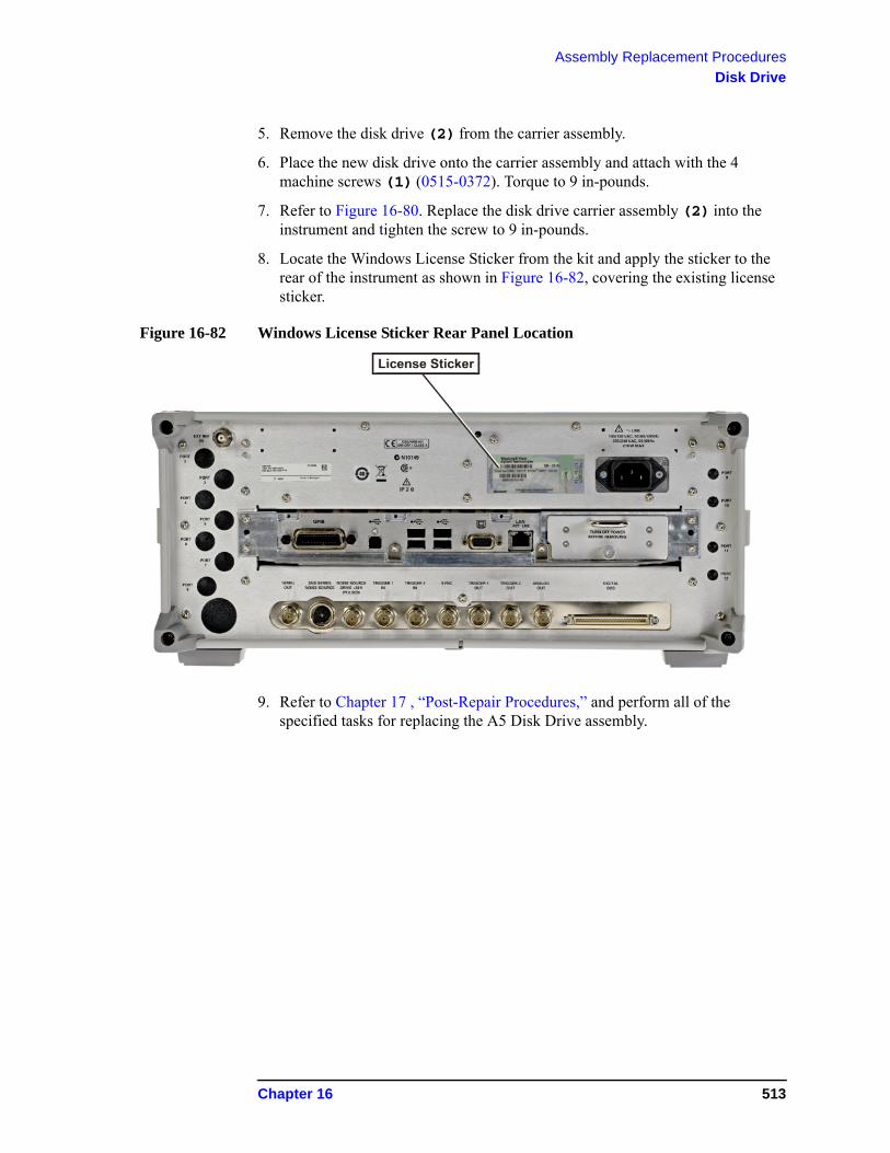
Assembly Replacement Procedures
Disk Drive
5. Remove the disk drive (2) from the carrier assembly.
6. Place the new disk drive onto the carrier assembly and attach with the 4 machine screws (1) (0515-0372). Torque to 9 in-pounds.
7. Refer to Figure 16-80. Replace the disk drive carrier assembly (2) into the instrument and tighten the screw to 9 in-pounds.
8. Locate the Windows License Sticker from the kit and apply the sticker to the rear of the instrument as shown in Figure 16-82, covering the existing license sticker.
Figure 16-82 Windows License Sticker Rear Panel Location
9. Refer to Chapter 17 , “Post-Repair Procedures,” and perform all of the specified tasks for replacing the A5 Disk Drive assembly.
Chapter 16 513
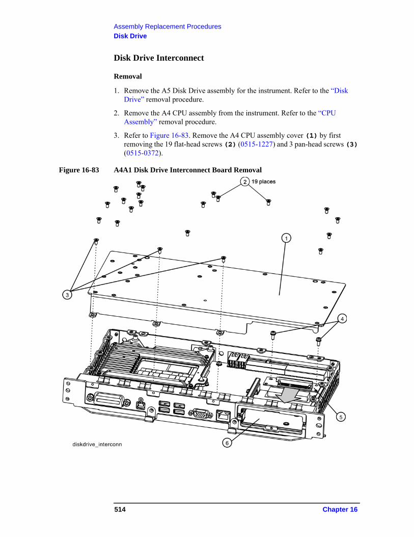
Assembly Replacement Procedures
Disk Drive
Disk Drive Interconnect
Removal
1. Remove the A5 Disk Drive assembly for the instrument. Refer to the “Disk Drive” removal procedure.
2. Remove the A4 CPU assembly from the instrument. Refer to the “CPU Assembly” removal procedure.
3. Refer to Figure 16-83. Remove the A4 CPU assembly cover (1) by first removing the 19 flat-head screws (2) (0515-1227) and 3 pan-head screws (3) (0515-0372).
Figure 16-83 A4A1 Disk Drive Interconnect Board Removal
514 Chapter 16
Assembly Replacement Procedures
Disk Drive
4. Remove the 2 screws (4) (0515-0372) that attached the A4A1 Disk Drive Interconnect board (5) to the A4 CPU assembly.
5. Unplug and remove the A4A1 Disk Drive Interconnect board from the A4 CPU assembly by carefully sliding the board out towards the disk drive bay opening (6).
Installation
1. Refer to Figure 16-83. Plug the A4A1 Disk Drive Interconnect board (5) into the A4 CPU assembly by carefully sliding it into place from the disk drive bay opening (6).
2. Install the 2 screws (4) (0515-0372) that secure the A4A1 Disk Drive Interconnect board to the A4 CPU assembly and torque them to 9 inch-pounds.
3. Replace the A4 CPU assembly cover (1) and attach it with the 19 flat-head screws (2) (0515-1227) and the 3 pan-head screws (3) (0515-0372). Torque all screws to 9 inch-pounds.
4. Re-install the A4 CPU assembly into the instrument. Refer to the CPU Assembly installation procedure.
5. Re-install the A5 Disk Drive assembly into the instrument. Refer to the Disk Drive installation procedure.
Chapter 16 515
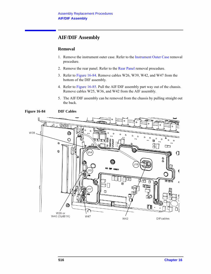
Assembly Replacement Procedures
AIF/DIF Assembly
AIF/DIF Assembly
Removal
1. Remove the instrument outer case. Refer to the Instrument Outer Case removal procedure.
2. Remove the rear panel. Refer to the Rear Panel removal procedure.
3. Refer to Figure 16-84. Remove cables W26, W39, W42, and W47 from the bottom of the DIF assembly.
4. Refer to Figure 16-85. Pull the AIF/DIF assembly part way out of the chassis. Remove cables W25, W36, and W42 from the AIF assembly.
5. The AIF/DIF assembly can be removed from the chassis by pulling straight out the back.
Figure 16-84 DIF Cables
516 Chapter 16
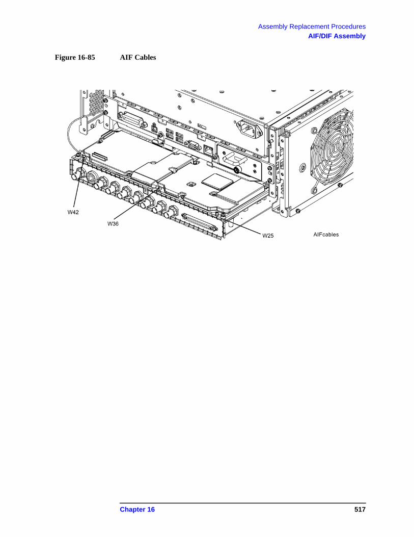
Assembly Replacement Procedures
AIF/DIF Assembly
Figure 16-85 AIF Cables
Chapter 16 517
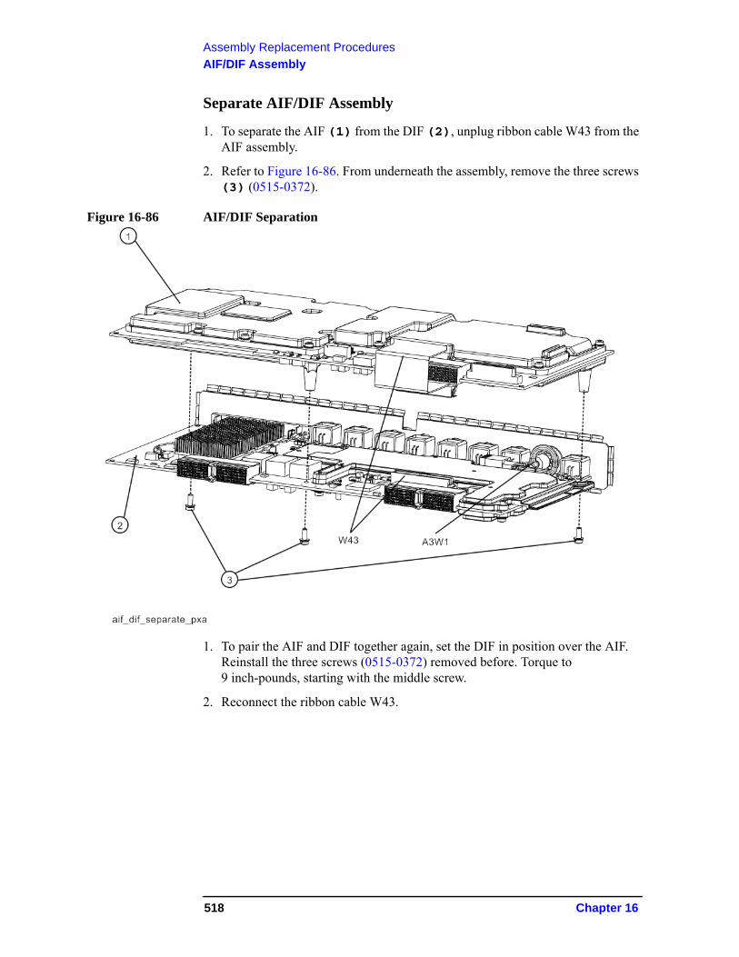
Assembly Replacement Procedures
AIF/DIF Assembly
Separate AIF/DIF Assembly
1. To separate the AIF (1) from the DIF (2), unplug ribbon cable W43 from the AIF assembly.
2. Refer to Figure 16-86. From underneath the assembly, remove the three screws (3) (0515-0372).
Figure 16-86 AIF/DIF Separation
1. To pair the AIF and DIF together again, set the DIF in position over the AIF. Reinstall the three screws (0515-0372) removed before. Torque to 9 inch-pounds, starting with the middle screw.
2. Reconnect the ribbon cable W43.
518 Chapter 16
Assembly Replacement Procedures
AIF/DIF Assembly
Replacement
1. Slide the AIF/DIF assembly into the slot at the rear of the instrument and push on the assembly to mate the connectors to the motherboard assembly.
2. Refer to Figure 16-85. Replace cables W25, W36, and W42 to the AIF assembly.
3. Refer to Figure 16-84. Replace cable W26, W39, W42, and W47 to the bottom of the DIF assembly.
4. Replace the rear panel. Refer to the Rear Panel replacement procedure.
5. Replace the instrument outer case. Refer to the Instrument Outer Case replacement procedure.
Chapter 16 519
Assembly Replacement Procedures
Motherboard Assembly
Motherboard Assembly
Removal
1. Remove the instrument outer case. Refer to the Instrument Outer Case removal procedure.
2. Remove the rear panel. Refer to the Rear Panel removal procedure.
3. Remove the top brace and power supply bracket. Refer to the Top Brace and Power Supply Bracket removal procedure.
4. Remove the Front Frame Assembly. Refer to the Front Frame Assembly removal procedure.
5. Remove the reference assembly. Refer to the Reference Assembly removal procedure.
6. If Option B1X is present in the instrument, remove the two option boards.
7. Remove the CPU assembly. Refer to the CPU Assembly removal procedure.
8. Remove the power supply assembly. Refer to the Power Supply Assembly removal procedure.
9. Remove the AIF/DIF assembly. Refer to the AIF/DIF Assembly removal procedure.
10.Remove the Front End Control assembly. Refer to the Front End Control Assembly removal procedure.
11. Remove the LO Synthesizer assembly. Refer to the LO Synthesizer Assembly removal procedure.
12.Remove the Midplane assembly. Refer to the Midplane Board Assembly removal procedure.
13.Remove the RF bracket. Refer to Figure 16-7 on page 437.
14.Remove the fan assembly. Refer to the Fan Assembly removal procedure.
15.Refer to Figure 16-87 and Figure 16-88. Remove the midplane bracket (1) by removing the eight screws (2) (0515-0372) (two on each side and four on the bottom).
520 Chapter 16
Assembly Replacement Procedures
Motherboard Assembly
Figure 16-87 Midplane Bracket Removal
Figure 16-88 Bottom Screws
Chapter 16 521
Assembly Replacement Procedures
Motherboard Assembly
16.Refer to Figure 16-89. Remove the left side chassis (1) (same side as the fan) by removing the nine screws (2) (0515-0372) (six on the bottom).
Figure 16-89 Chassis Side Removal
522 Chapter 16
Assembly Replacement Procedures
Motherboard Assembly
17.Refer to Figure 16-90. Remove the motherboard (1) by removing the four screws (2) (0515-0372). Slide the motherboard back off the standoffs and lift it up and out.
Figure 16-90 Motherboard Assembly Removal
Chapter 16 523
Assembly Replacement Procedures
Motherboard Assembly
Replacement
1. Refer to Figure 16-90. Place the motherboard (1) on standoffs and slide into position in the chassis and replace the four screws (2) (0515-0372). Torque to 9 inch-pounds.
2. Refer to Figure 16-89. Replace the left side chassis by replacing the nine screws (0515-0372). Torque to 9 inch-pounds.
3. Refer to Figure 16-87. Replace the midplane bracket (1) by replacing the eight screws (2) (0515-0372). Torque to 9 inch-pounds.
4. Replace the fan assembly. Refer to the Fan Assembly replacement procedure.
5. Replace the Midplane assembly. Refer to the Midplane Board Assembly replacement procedure.
6. Replace the Front End Control assembly. Refer to the Front End Control Assembly replacement procedure.
7. Replace the LO Synthesizer assembly. Refer to the LO Synthesizer Assembly replacement procedure.
8. Replace the AIF/DIF assembly. Refer to the AIF/DIF Assembly replacement procedure.
9. Replace the CPU assembly. Refer to the CPU Assembly replacement procedure.
10.Replace the power supply assembly. Refer to the Power Supply Assembly replacement procedure.
11. Replace the reference assembly. Refer to the Reference Assembly replacement procedure.
12.Replace the rear panel. Refer to the Rear Panel replacement procedure.
13. If Option B1X is present in the instrument, install the two option boards.
14.Ensure all cables are plugged in or connected and torqued.
15.Replace the RF bracket. Refer to Figure 16-7 on page 437. Torque the screws to 9 inch-pounds.
16.Replace the Front Frame Assembly. Refer to the Front Frame Assembly replacement procedure.
17.Replace the top brace and reference bracket. Refer to the Top Brace and Power Supply Bracket replacement procedure.
18.Replace the instrument outer case. Refer to the Instrument Outer Case replacement procedure.
524 Chapter 16
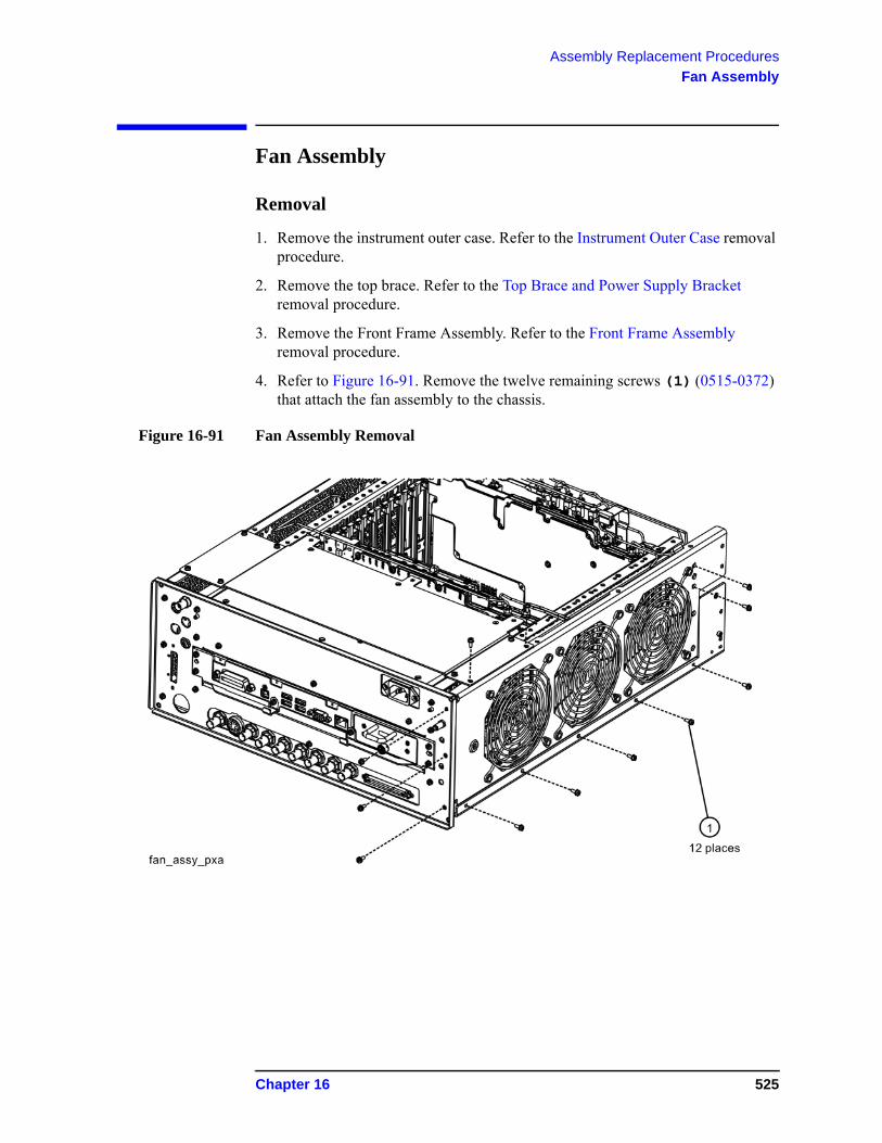
Assembly Replacement Procedures
Fan Assembly
Fan Assembly
Removal
1. Remove the instrument outer case. Refer to the Instrument Outer Case removal procedure.
2. Remove the top brace. Refer to the Top Brace and Power Supply Bracket removal procedure.
3. Remove the Front Frame Assembly. Refer to the Front Frame Assembly removal procedure.
4. Refer to Figure 16-91. Remove the twelve remaining screws (1) (0515-0372) that attach the fan assembly to the chassis.
Figure 16-91 Fan Assembly Removal
Chapter 16 525
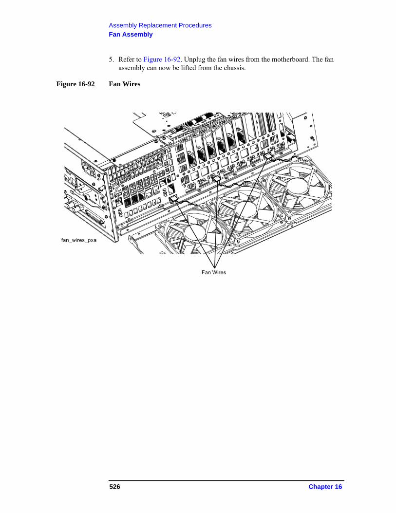
Assembly Replacement Procedures
Fan Assembly
5. Refer to Figure 16-92. Unplug the fan wires from the motherboard. The fan assembly can now be lifted from the chassis.
Figure 16-92 Fan Wires
526 Chapter 16
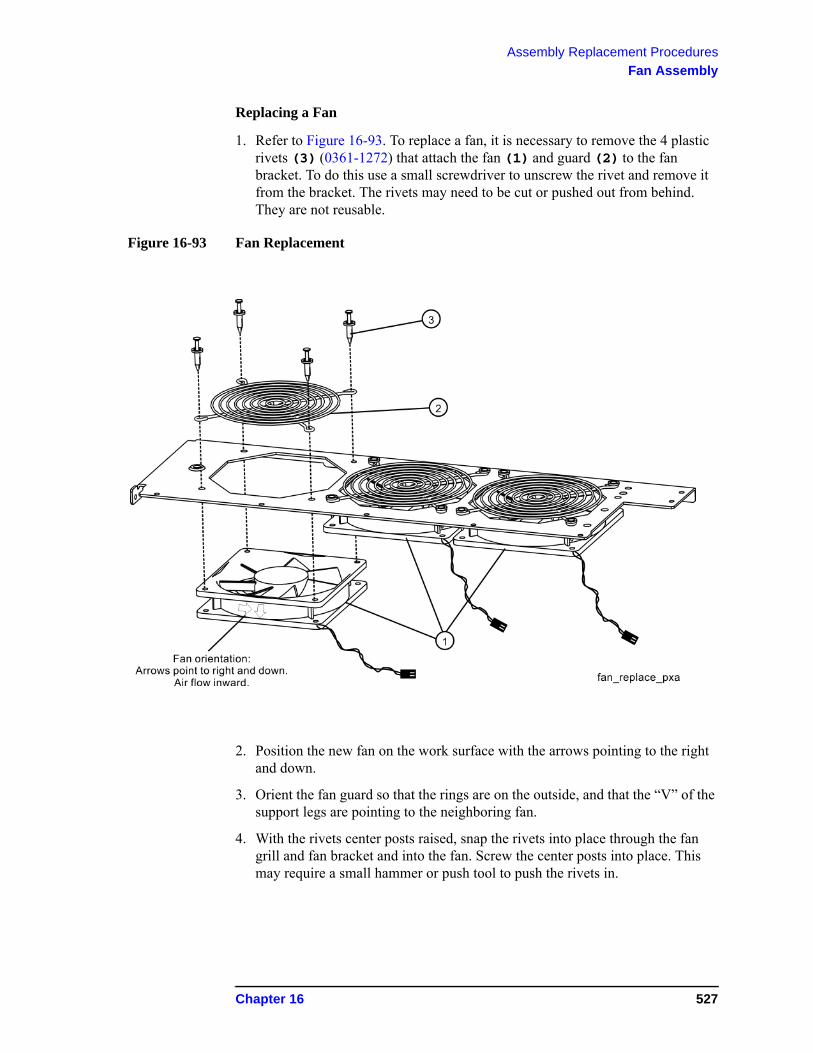
Assembly Replacement Procedures
Fan Assembly
Replacing a Fan
1. Refer to Figure 16-93. To replace a fan, it is necessary to remove the 4 plastic rivets (3) (0361-1272) that attach the fan (1) and guard (2) to the fan bracket. To do this use a small screwdriver to unscrew the rivet and remove it from the bracket. The rivets may need to be cut or pushed out from behind. They are not reusable.
Figure 16-93 Fan Replacement
2. Position the new fan on the work surface with the arrows pointing to the right and down.
3. Orient the fan guard so that the rings are on the outside, and that the “V” of the support legs are pointing to the neighboring fan.
4. With the rivets center posts raised, snap the rivets into place through the fan grill and fan bracket and into the fan. Screw the center posts into place. This may require a small hammer or push tool to push the rivets in.
Chapter 16 527
Assembly Replacement Procedures
Fan Assembly
Replacement
1. Plug the fan wires into the motherboard.
2. Refer to Figure 16-91. Place the fan assembly into position in the chassis. Replace the twelve screws (1) (0515-0372) to attach the fan assembly to the chassis. Ensure the fan wires are not pinched. Torque to 9 inch-pounds.
3. Replace the Front Frame Assembly. Refer to the Front Frame Assembly replacement procedure.
4. Replace the top brace. Refer to the Top Brace and Power Supply Bracket replacement procedure.
5. Replace the instrument outer case. Refer to the Instrument Outer Case replacement procedure.
528 Chapter 16
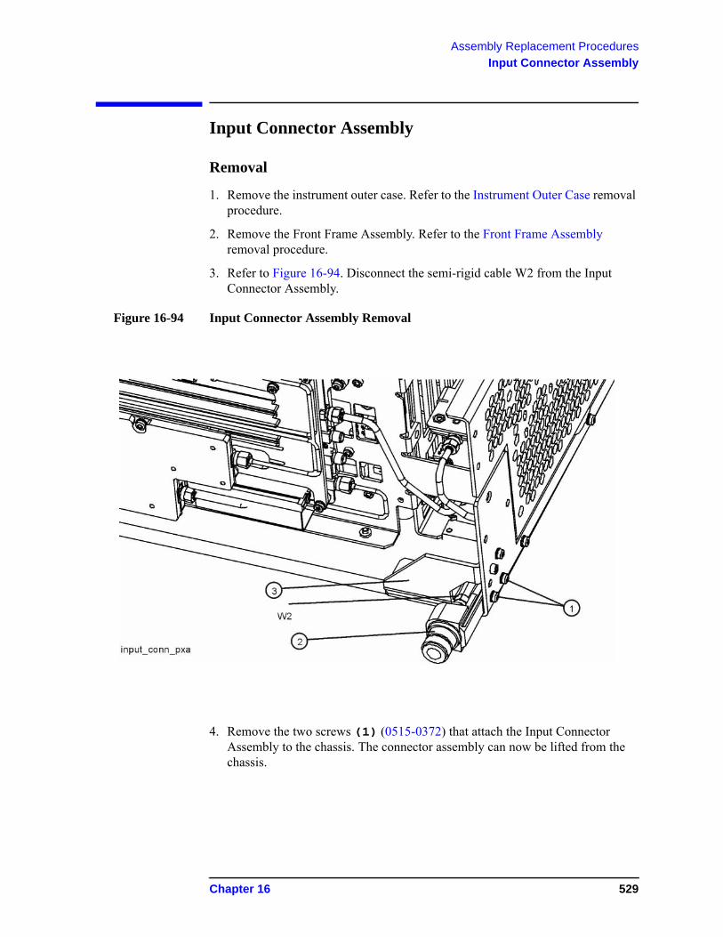
Assembly Replacement Procedures
Input Connector Assembly
Input Connector Assembly
Removal
1. Remove the instrument outer case. Refer to the Instrument Outer Case removal procedure.
2. Remove the Front Frame Assembly. Refer to the Front Frame Assembly removal procedure.
3. Refer to Figure 16-94. Disconnect the semi-rigid cable W2 from the Input Connector Assembly.
Figure 16-94 Input Connector Assembly Removal
4. Remove the two screws (1) (0515-0372) that attach the Input Connector Assembly to the chassis. The connector assembly can now be lifted from the chassis.
Chapter 16 529
Assembly Replacement Procedures
Input Connector Assembly
Replacement
1. Refer to Figure 16-94. Place the Input Connector Assembly into position in the chassis. Replace the two screws (1) (0515-0372) to attach the Input Connector Assembly to the chassis. Torque to 9 inch-pounds.
2. Reconnect the semi-rigid cable W2 to the Input Connector Assembly. Torque to 10 inch-pounds.
3. Replace the Front Frame Assembly. Refer to the Front Frame Assembly replacement procedure.
4. Replace the instrument outer case. Refer to the Instrument Outer Case replacement procedure.
530 Chapter 16
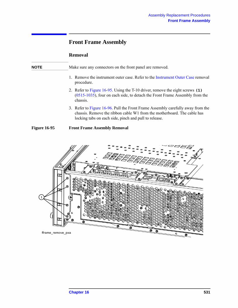
Assembly Replacement Procedures
Front Frame Assembly
Front Frame Assembly
Removal
NOTE Make sure any connectors on the front panel are removed.
1. Remove the instrument outer case. Refer to the Instrument Outer Case removal procedure.
2. Refer to Figure 16-95. Using the T-10 driver, remove the eight screws (1) (0515-1035), four on each side, to detach the Front Frame Assembly from the chassis.
3. Refer to Figure 16-96. Pull the Front Frame Assembly carefully away from the chassis. Remove the ribbon cable W1 from the motherboard. The cable has locking tabs on each side, pinch and pull to release.
Figure 16-95 Front Frame Assembly Removal
Chapter 16 531
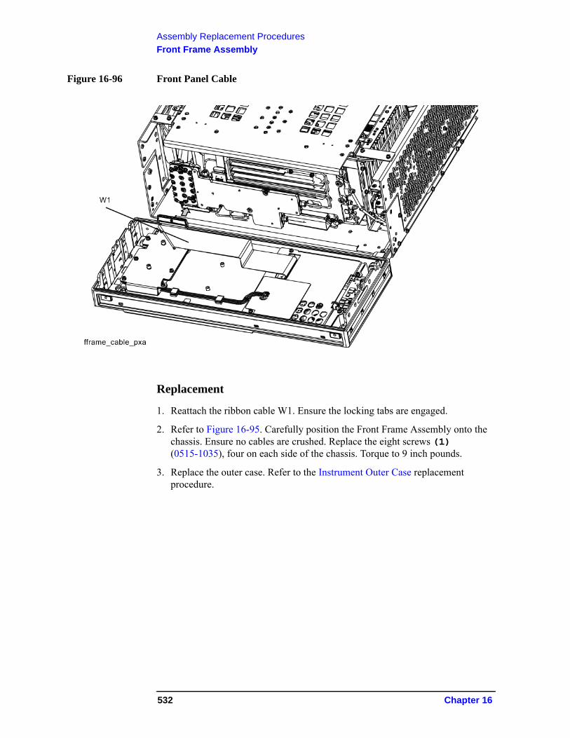
Assembly Replacement Procedures
Front Frame Assembly
Figure 16-96 Front Panel Cable
Replacement
1. Reattach the ribbon cable W1. Ensure the locking tabs are engaged.
2. Refer to Figure 16-95. Carefully position the Front Frame Assembly onto the chassis. Ensure no cables are crushed. Replace the eight screws (1) (0515-1035), four on each side of the chassis. Torque to 9 inch pounds.
3. Replace the outer case. Refer to the Instrument Outer Case replacement procedure.
532 Chapter 16
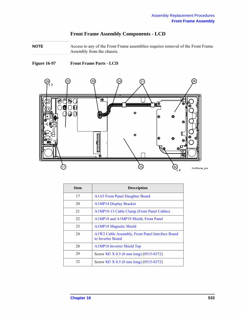
Assembly Replacement Procedures
Front Frame Assembly
Front Frame Assembly Components - LCD
NOTE Access to any of the Front Frame assemblies requires removal of the Front Frame Assembly from the chassis.
Figure 16-97 Front Frame Parts - LCD
Item Description
17 A1A5 Front Panel Daughter Board
20 A1MP14 Display Bracket
21 A1MP10-13 Cable Clamp (Front Panel Cables)
22 A1MP18 and A1MP19 Shield, Front Panel
23 A1MP18 Magnetic Shield
24 A1W2 Cable Assembly, Front Panel Interface Board to Inverter Board
28 A1MP16 Inverter Shield Top
29 Screw M3 X 0.5 (8 mm long) (0515-0372)
32 Screw M3 X 0.5 (8 mm long) (0515-0372)
Chapter 16 533
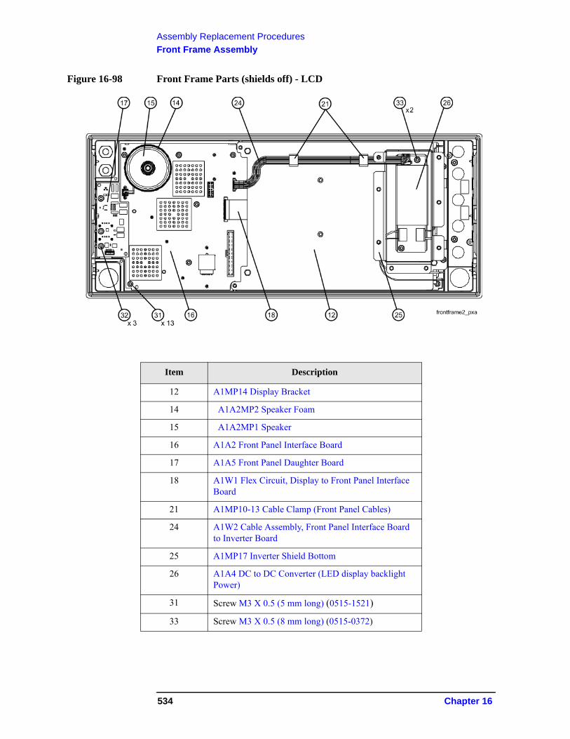
Assembly Replacement Procedures
Front Frame Assembly
Figure 16-98 Front Frame Parts (shields off) - LCD
Item Description
12 A1MP14 Display Bracket
14 A1A2MP2 Speaker Foam
15 A1A2MP1 Speaker
16 A1A2 Front Panel Interface Board
17 A1A5 Front Panel Daughter Board
18 A1W1 Flex Circuit, Display to Front Panel Interface Board
21 A1MP10-13 Cable Clamp (Front Panel Cables)
24 A1W2 Cable Assembly, Front Panel Interface Board to Inverter Board
25 A1MP17 Inverter Shield Bottom
26 A1A4 DC to DC Converter (LED display backlight Power)
31 Screw M3 X 0.5 (5 mm long) (0515-1521)
33 Screw M3 X 0.5 (8 mm long) (0515-0372)
534 Chapter 16
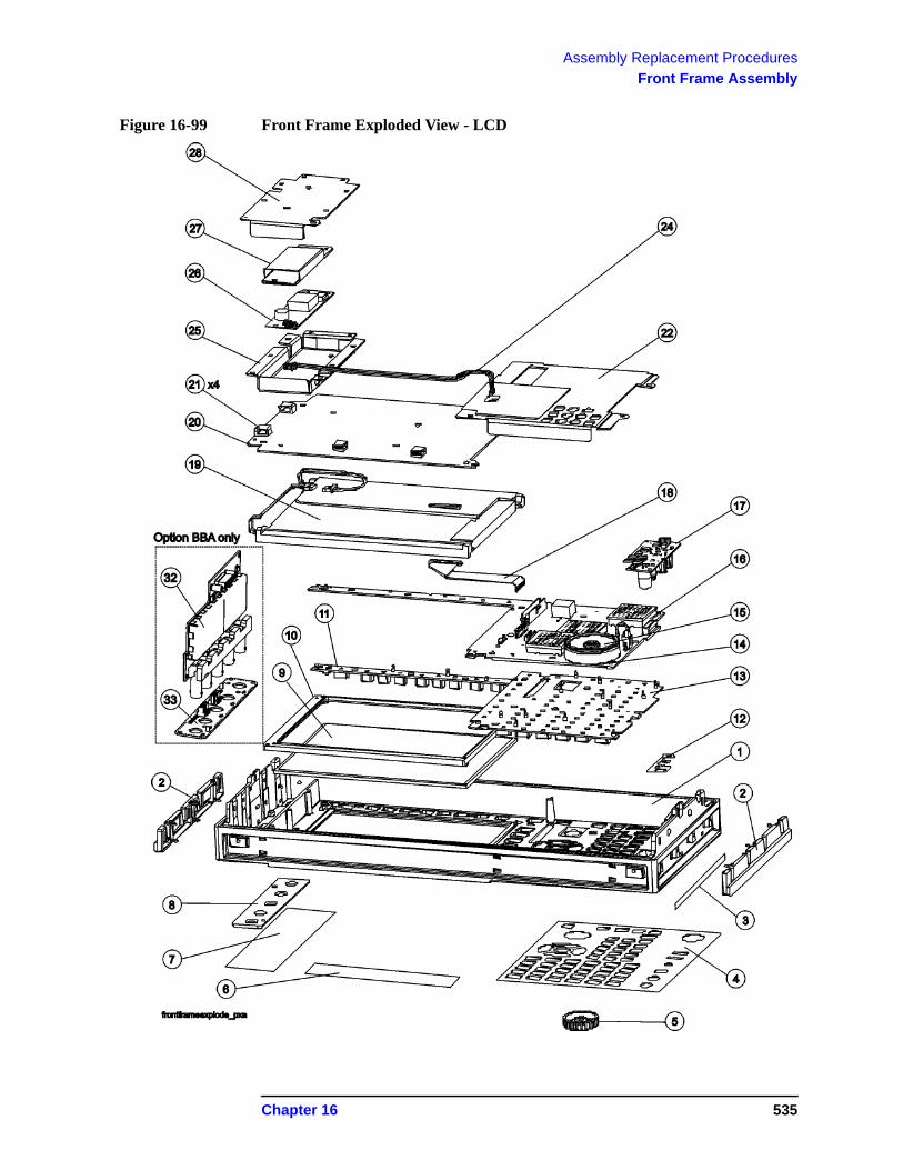
Assembly Replacement Procedures
Front Frame Assembly
Figure 16-99 Front Frame Exploded View - LCD
Chapter 16 535
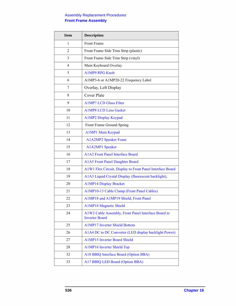
Assembly Replacement Procedures
Front Frame Assembly
Item Description
1 Front Frame
2 Front Frame Side Trim Strip (plastic)
3 Front Frame Side Trim Strip (vinyl)
4 Main Keyboard Overlay
5 A1MP9 RPG Knob
6 A1MP3-6 or A1MP20-22 Frequency Label
7 Overlay, Left Display
8 Cover Plate
9 A1MP7 LCD Glass Filter
10 A1MP8 LCD Lens Gasket
11 A1MP2 Display Keypad
12 Front Frame Ground Spring
13 A1MP1 Main Keypad
14 A1A2MP2 Speaker Foam
15 A1A2MP1 Speaker
16 A1A2 Front Panel Interface Board
17 A1A5 Front Panel Daughter Board
18 A1W1 Flex Circuit, Display to Front Panel Interface Board
19 A1A3 Liquid Crystal Display (fluorescent backlight),
20 A1MP14 Display Bracket
21 A1MP10-13 Cable Clamp (Front Panel Cables)
22 A1MP18 and A1MP19 Shield, Front Panel
23 A1MP18 Magnetic Shield
24 A1W2 Cable Assembly, Front Panel Interface Board to Inverter Board
25 A1MP17 Inverter Shield Bottom
26 A1A4 DC to DC Converter (LED display backlight Power)
27 A1MP15 Inverter Board Shield
28 A1MP16 Inverter Shield Top
32 A18 BBIQ Interface Board (Option BBA)
33 A17 BBIQ LED Board (Option BBA)
536 Chapter 16
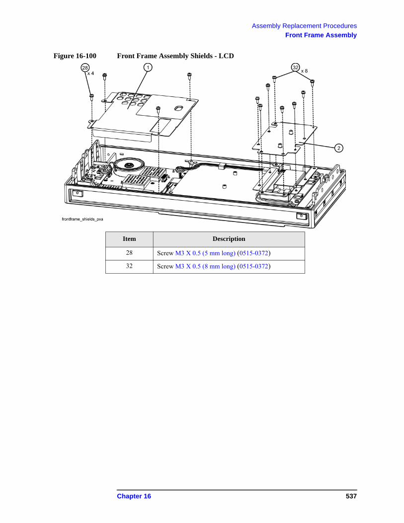
Assembly Replacement Procedures
Front Frame Assembly
Figure 16-100 Front Frame Assembly Shields - LCD
Item Description
28 Screw M3 X 0.5 (5 mm long) (0515-0372)
32 Screw M3 X 0.5 (8 mm long) (0515-0372)
Chapter 16 537
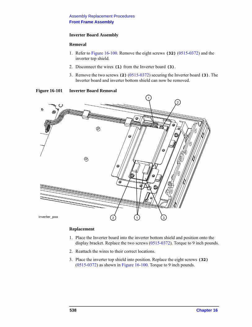
Assembly Replacement Procedures
Front Frame Assembly
Inverter Board Assembly
Removal
1. Refer to Figure 16-100. Remove the eight screws (32) (0515-0372) and the inverter top shield.
2. Disconnect the wires (1) from the Inverter board (3).
3. Remove the two screws (2) (0515-0372) securing the Inverter board (3). The Inverter board and inverter bottom shield can now be removed.
Figure 16-101 Inverter Board Removal
Replacement
1. Place the Inverter board into the inverter bottom shield and position onto the display bracket. Replace the two screws (0515-0372). Torque to 9 inch pounds.
2. Reattach the wires to their correct locations.
3. Place the inverter top shield into position. Replace the eight screws (32) (0515-0372) as shown in Figure 16-100. Torque to 9 inch pounds.
538 Chapter 16
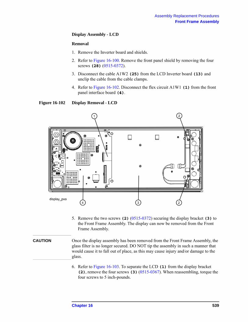
Assembly Replacement Procedures
Front Frame Assembly
Display Assembly - LCD
Removal
1. Remove the Inverter board and shields.
2. Refer to Figure 16-100. Remove the front panel shield by removing the four screws (28) (0515-0372).
3. Disconnect the cable A1W2 (25) from the LCD Inverter board (13) and unclip the cable from the cable clamps.
4. Refer to Figure 16-102. Disconnect the flex circuit A1W1 (1) from the front panel interface board (4).
Figure 16-102 Display Removal - LCD
5. Remove the two screws (2) (0515-0372) securing the display bracket (3) to the Front Frame Assembly. The display can now be removed from the Front Frame Assembly.
CAUTION Once the display assembly has been removed from the Front Frame Assembly, the glass filter is no longer secured. DO NOT tip the assembly in such a manner that would cause it to fall out of place, as this may cause injury and/or damage to the glass.
6. Refer to Figure 16-103. To separate the LCD (1) from the display bracket (2), remove the four screws (3) (0515-0367). When reassembling, torque the four screws to 5 inch-pounds.
Chapter 16 539
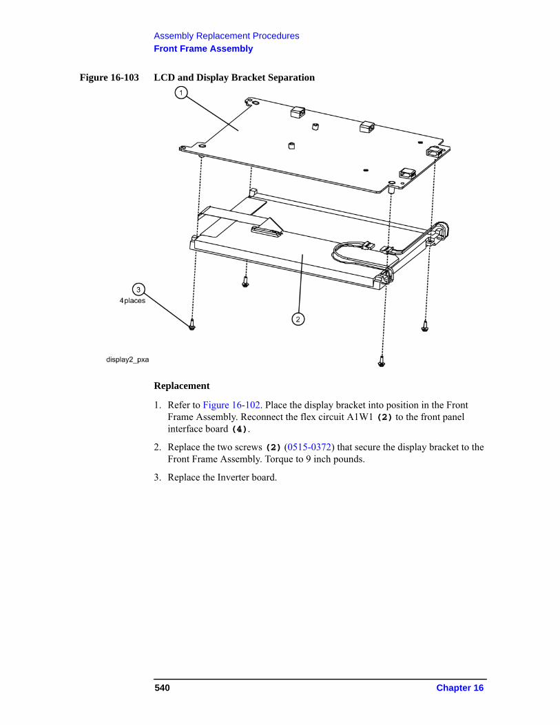
Assembly Replacement Procedures
Front Frame Assembly
Figure 16-103 LCD and Display Bracket Separation
Replacement
1. Refer to Figure 16-102. Place the display bracket into position in the Front Frame Assembly. Reconnect the flex circuit A1W1 (2) to the front panel interface board (4).
2. Replace the two screws (2) (0515-0372) that secure the display bracket to the Front Frame Assembly. Torque to 9 inch pounds.
3. Replace the Inverter board.
540 Chapter 16
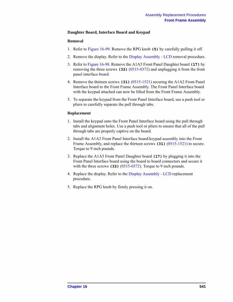
Assembly Replacement Procedures
Front Frame Assembly
Daughter Board, Interface Board and Keypad
Removal
1. Refer to Figure 16-99. Remove the RPG knob (5) by carefully pulling it off.
2. Remove the display. Refer to the Display Assembly - LCD removal procedure.
3. Refer to Figure 16-98. Remove the A1A5 Front Panel Daughter board (17) by removing the three screws (32) (0515-0372) and unplugging it from the front panel interface board.
4. Remove the thirteen screws (31) (0515-1521) securing the A1A2 Front Panel Interface board to the Front Frame Assembly. The Front Panel Interface board with the keypad attached can now be lifted from the Front Frame Assembly.
5. To separate the keypad from the Front Panel Interface board, use a push tool or pliers to carefully separate the pull through tabs.
Replacement
1. Install the keypad onto the Front Panel Interface board using the pull through tabs and alignment holes. Use a push tool or pliers to ensure that all of the pull through tabs are properly captive on the board.
2. Install the A1A2 Front Panel Interface board/keypad assembly into the Front Frame Assembly, and replace the thirteen screws (31) (0515-1521) to secure. Torque to 9 inch pounds.
3. Replace the A1A5 Front Panel Daughter board (17) by plugging it into the Front Panel Interface board using the board to board connectors and secure it with the three screws (32) (0515-0372). Torque to 9 inch pounds.
4. Replace the display. Refer to the Display Assembly - LCD replacement procedure.
5. Replace the RPG knob by firmly pressing it on.
Chapter 16 541
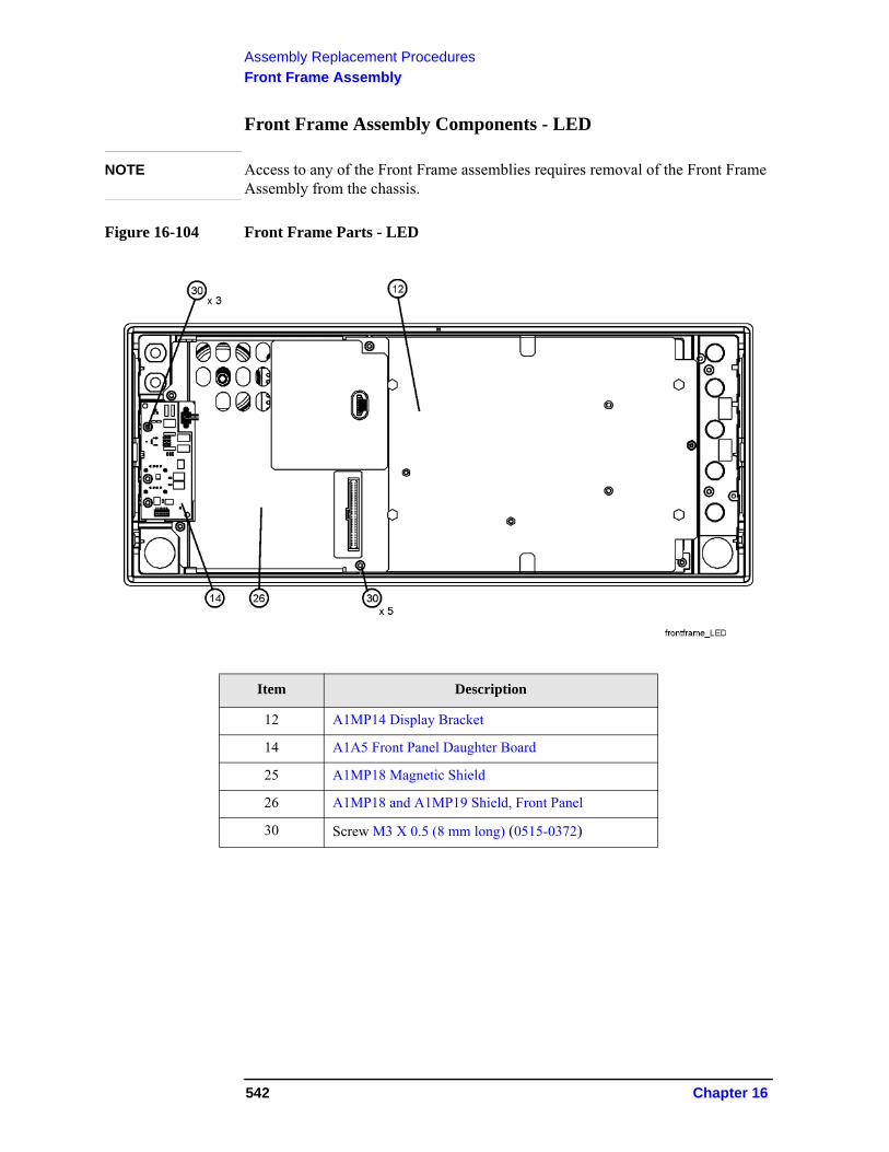
Assembly Replacement Procedures
Front Frame Assembly
Front Frame Assembly Components - LED
NOTE Access to any of the Front Frame assemblies requires removal of the Front Frame Assembly from the chassis.
Figure 16-104 Front Frame Parts - LED
Item Description
12 A1MP14 Display Bracket
14 A1A5 Front Panel Daughter Board
25 A1MP18 Magnetic Shield
26 A1MP18 and A1MP19 Shield, Front Panel
30 Screw M3 X 0.5 (8 mm long) (0515-0372)
542 Chapter 16
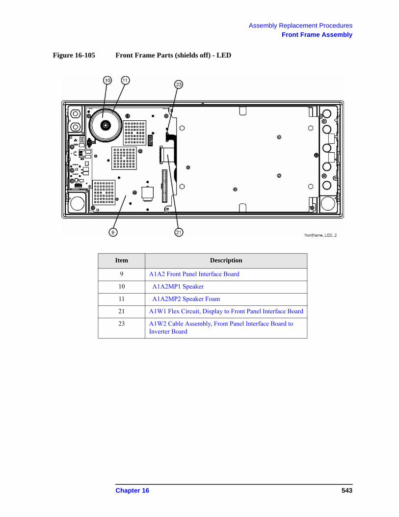
Assembly Replacement Procedures
Front Frame Assembly
Figure 16-105 Front Frame Parts (shields off) - LED
Item Description
9 A1A2 Front Panel Interface Board
10 A1A2MP1 Speaker
11 A1A2MP2 Speaker Foam
21 A1W1 Flex Circuit, Display to Front Panel Interface Board
23 A1W2 Cable Assembly, Front Panel Interface Board to Inverter Board
Chapter 16 543
Assembly Replacement Procedures
Front Frame Assembly
Figure 16-106 Front Frame Exploded View - LED
544 Chapter 16
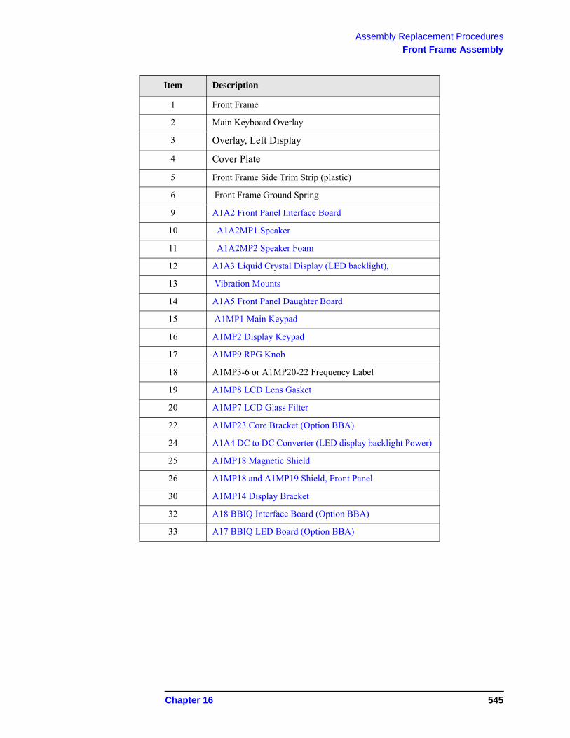
Assembly Replacement Procedures
Front Frame Assembly
Item Description
1 Front Frame
2 Main Keyboard Overlay
3 Overlay, Left Display
4 Cover Plate
5 Front Frame Side Trim Strip (plastic)
6 Front Frame Ground Spring
9 A1A2 Front Panel Interface Board
10 A1A2MP1 Speaker
11 A1A2MP2 Speaker Foam
12 A1A3 Liquid Crystal Display (LED backlight),
13 Vibration Mounts
14 A1A5 Front Panel Daughter Board
15 A1MP1 Main Keypad
16 A1MP2 Display Keypad
17 A1MP9 RPG Knob
18 A1MP3-6 or A1MP20-22 Frequency Label
19 A1MP8 LCD Lens Gasket
20 A1MP7 LCD Glass Filter
22 A1MP23 Core Bracket (Option BBA)
24 A1A4 DC to DC Converter (LED display backlight Power)
25 A1MP18 Magnetic Shield
26 A1MP18 and A1MP19 Shield, Front Panel
30 A1MP14 Display Bracket
32 A18 BBIQ Interface Board (Option BBA)
33 A17 BBIQ LED Board (Option BBA)
Chapter 16 545
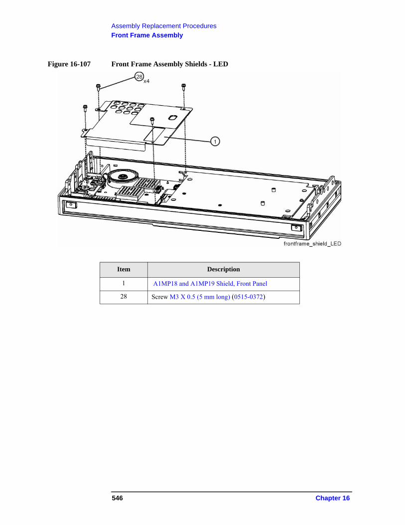
Assembly Replacement Procedures
Front Frame Assembly
Figure 16-107 Front Frame Assembly Shields - LED
Item Description
1 A1MP18 and A1MP19 Shield, Front Panel
28 Screw M3 X 0.5 (5 mm long) (0515-0372)
546 Chapter 16
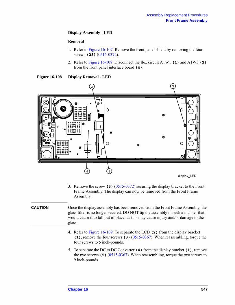
Assembly Replacement Procedures
Front Frame Assembly
Display Assembly - LED
Removal
1. Refer to Figure 16-107. Remove the front panel shield by removing the four screws (28) (0515-0372).
2. Refer to Figure 16-108. Disconnect the flex circuit A1W1 (1) and A1W3 (2) from the front panel interface board (4).
Figure 16-108 Display Removal - LED
3. Remove the screw (3) (0515-0372) securing the display bracket to the Front Frame Assembly. The display can now be removed from the Front Frame Assembly.
CAUTION Once the display assembly has been removed from the Front Frame Assembly, the glass filter is no longer secured. DO NOT tip the assembly in such a manner that would cause it to fall out of place, as this may cause injury and/or damage to the glass.
4. Refer to Figure 16-109. To separate the LCD (2) from the display bracket (1), remove the four screws (3) (0515-0367). When reassembling, torque the four screws to 5 inch-pounds.
5. To separate the DC to DC Converter (4) from the display bracket (1), remove the two screws (5) (0515-0367). When reassembling, torque the two screws to 9 inch-pounds.
Chapter 16 547
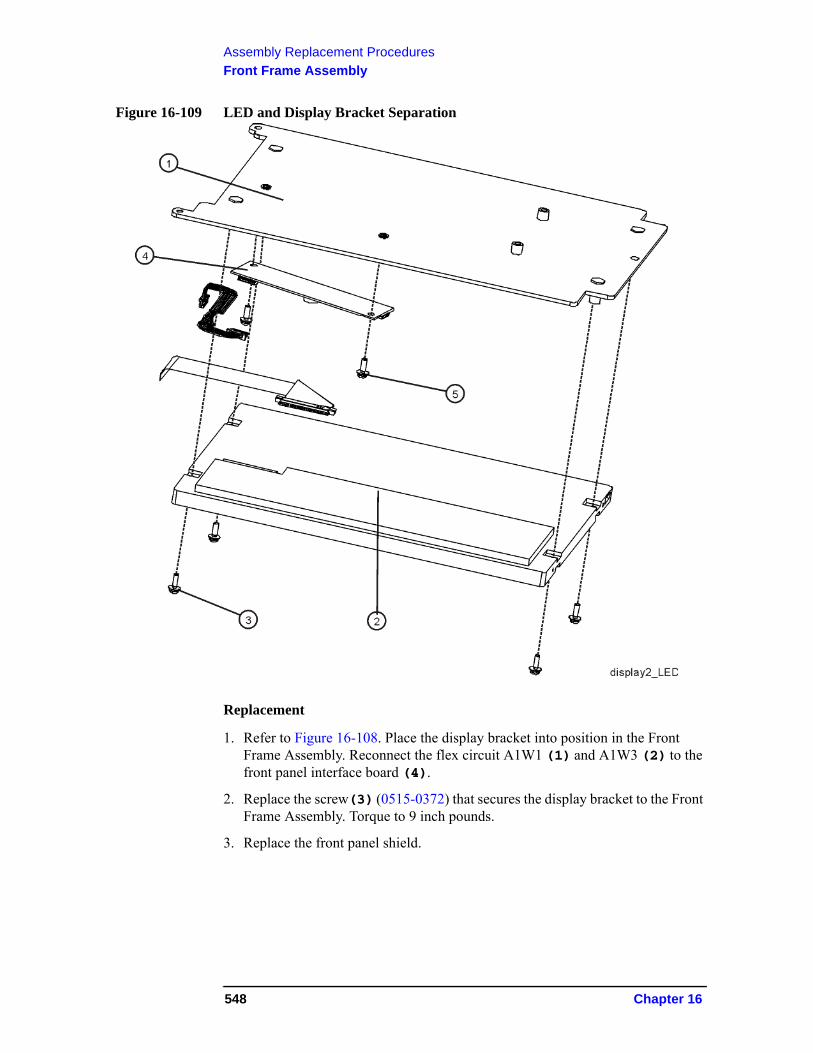
Assembly Replacement Procedures
Front Frame Assembly
Figure 16-109 LED and Display Bracket Separation
Replacement
1. Refer to Figure 16-108. Place the display bracket into position in the Front Frame Assembly. Reconnect the flex circuit A1W1 (1) and A1W3 (2) to the front panel interface board (4).
2. Replace the screw(3) (0515-0372) that secures the display bracket to the Front Frame Assembly. Torque to 9 inch pounds.
3. Replace the front panel shield.
548 Chapter 16
Assembly Replacement Procedures
Front Frame Assembly
Daughter Board, Interface Board and Keypad
Removal
1. Refer to Figure 16-106. Remove the RPG knob (17) by carefully pulling it off.
2. Remove the display. Refer to the Display Assembly - LCD removal procedure.
3. Refer to Figure 16-104. Remove the A1A5 Front Panel Daughter board (14) by removing the three screws (30) (0515-0372) and unplugging it from the front panel interface board.
4. Remove the thirteen screws (0515-1521) securing the A1A2 Front Panel Interface board to the Front Frame Assembly. The Front Panel Interface board with the keypad attached can now be lifted from the Front Frame Assembly.
5. To separate the keypad from the Front Panel Interface board, use a push tool or pliers to carefully separate the pull through tabs.
Replacement
1. Install the keypad onto the Front Panel Interface board using the pull through tabs and alignment holes. Use a push tool or pliers to ensure that all of the pull through tabs are properly captive on the board.
2. Install the A1A2 Front Panel Interface board/keypad assembly into the Front Frame Assembly, and replace the thirteen screws (0515-1521) to secure. Torque to 9 inch pounds.
3. Replace the A1A5 Front Panel Daughter board (14) by plugging it into the Front Panel Interface board using the board to board connectors and secure it with the three screws (30) (0515-0372). Torque to 9 inch pounds.
4. Replace the display. Refer to the Display Assembly - LCD replacement procedure.
5. Replace the RPG knob by firmly pressing it on.
Chapter 16 549

Assembly Replacement Procedures
Front Frame Assembly
550 Chapter 16
17 Post-Repair Procedures
551
Post-Repair Procedures
What You Will Find in This Chapter
What You Will Find in This Chapter
This chapter provides information that will enable you to return an instrument to full operation following the replacement of any instrument assembly. This information includes a table that shows which adjustments and/or performance tests must be executed after replacing an assembly.
Before Starting
There are three things you should do before starting any of the procedures listed or described in this chapter:
❏ Familiarize yourself with the safety symbols, and read the general safety considerations and the safety note definitions in the front of this guide, before you begin the procedures in this chapter.
❏ Check that the analyzer has been turned on and allowed to warm up.
❏ Ensure that the analyzer is operating within a temperature range of 20 °C to 30 °C.
Test equipment you will need
Refer to Table 1-1 on page 30, for a list of recommended equipment and critical test equipment specifications for the performance verification and adjustments.
552 Chapter 17
Post-Repair Procedures
Post-Repair Procedures
Post-Repair Procedures
Table 17-1 lists the adjustments and performance verification tests needed after an assembly replacement.
After an assembly is replaced, find the assembly that has been replaced in the left-hand column, and then perform the recommended adjustment and/or performance verification test. Making the recommended adjustments and/or performance verification tests doesn’t guarantee all published specifications are being met. Only a full instrument calibration will do this.
NOTE Refer to the analyzer user’s guide for information on instrument warm-up before performing any of the procedures listed in this chapter.
The following procedures are also included in the “Additional Tasks” on page 557.
• “Calibration Data Backup and Restore”
• “BIOS Settings Verification”
• “End User License Agreement (EULA) Acceptance”
• “FPGA Synchronization”
• “Programming Model and Serial Numbers”
Chapter 17 553
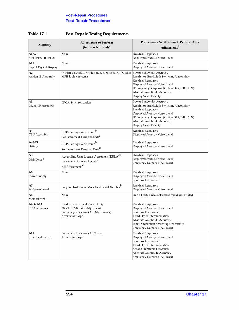
Post-Repair Procedures
Post-Repair Procedures
Table 17-1 Post-Repair Testing Requirements
AssemblyAdjustments to Perform
(in the order listed)a
Performance Verifications to Perform After
Adjustmentsa
A1A2 Front Panel Interface
None Residual ResponsesDisplayed Average Noise Level
A1A3 Liquid Crystal Display
None Residual ResponsesDisplayed Average Noise Level
A2 Analog IF Assembly
IF Flatness Adjust (Option B25, B40, or B1X if Option MPB is also present)
Power Bandwidth AccuracyResolution Bandwidth Switching UncertaintyResidual ResponsesDisplayed Average Noise LevelIF Frequency Response (Option B25, B40, B1X)Absolute Amplitude AccuracyDisplay Scale Fidelity
A3 Digital IF Assembly
FPGA Synchronizationb Power Bandwidth AccuracyResolution Bandwidth Switching UncertaintyResidual ResponsesDisplayed Average Noise LevelIF Frequency Response (Option B25, B40, B1X)Absolute Amplitude AccuracyDisplay Scale Fidelity
A4 CPU Assembly
BIOS Settings Verificationb
Set Instrument Time and Datec
Residual ResponsesDisplayed Average Noise Level
A4BT1 Battery
BIOS Settings Verificationb
Set Instrument Time and Datec
Residual ResponsesDisplayed Average Noise Level
A5
Disk DrivedAccept End User License Agreement (EULA)b
Instrument Software Updatee
All Adjustmentsdf
Residual ResponsesDisplayed Average Noise LevelFrequency Response (All Tests)
A6 Power Supply
None Residual ResponsesDisplayed Average Noise LevelSpurious Responses
A7 Midplane board
Program Instrument Model and Serial Numberb Residual ResponsesDisplayed Average Noise Level
A8 Motherboard
None Run all tests since instrument was disassembled.
A9 & A10 RF Attenuators
Hardware Statistical Reset Utility50 MHz Calibrator AdjustmentFrequency Response (All Adjustments)Attenuator Slope
Residual ResponsesDisplayed Average Noise LevelSpurious ResponsesThird Order IntermodulationAbsolute Amplitude AccuracyInput Attenuation Switching UncertaintyFrequency Response (All Tests)
A11 Low Band Switch
Frequency Response (All Tests)Attenuator Slope
Residual ResponsesDisplayed Average Noise LevelSpurious ResponsesThird Order IntermodulationSecond Harmonic DistortionAbsolute Amplitude AccuracyFrequency Response (All Tests)
554 Chapter 17
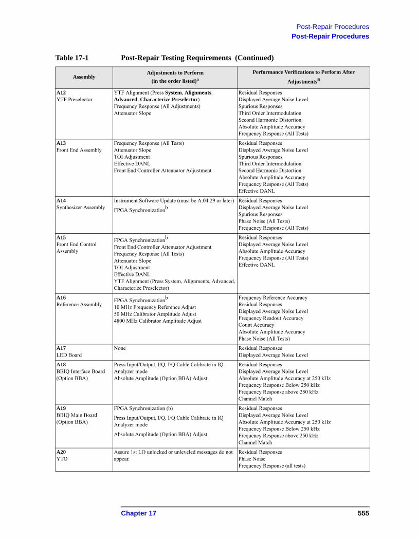
Post-Repair Procedures
Post-Repair Procedures
A12 YTF Preselector
YTF Alignment (Press System, Alignments, Advanced, Characterize Preselector)Frequency Response (All Adjustments)Attenuator Slope
Residual ResponsesDisplayed Average Noise LevelSpurious ResponsesThird Order IntermodulationSecond Harmonic DistortionAbsolute Amplitude AccuracyFrequency Response (All Tests)
A13 Front End Assembly
Frequency Response (All Tests)Attenuator SlopeTOI AdjustmentEffective DANLFront End Controller Attenuator Adjustment
Residual ResponsesDisplayed Average Noise LevelSpurious ResponsesThird Order IntermodulationSecond Harmonic DistortionAbsolute Amplitude AccuracyFrequency Response (All Tests)Effective DANL
A14 Synthesizer Assembly
Instrument Software Update (must be A.04.29 or later)
FPGA SynchronizationbResidual ResponsesDisplayed Average Noise LevelSpurious ResponsesPhase Noise (All Tests)Frequency Response (All Tests)
A15 Front End Control Assembly
FPGA Synchronizationb
Front End Controller Attenuator AdjustmentFrequency Response (All Tests)Attenuator SlopeTOI AdjustmentEffective DANLYTF Alignment (Press System, Alignments, Advanced, Characterize Preselector)
Residual ResponsesDisplayed Average Noise LevelAbsolute Amplitude AccuracyFrequency Response (All Tests)Effective DANL
A16 Reference Assembly
FPGA Synchronizationb
10 MHz Frequency Reference Adjust50 MHz Calibrator Amplitude Adjust4800 MHz Calibrator Amplitude Adjust
Frequency Reference AccuracyResidual ResponsesDisplayed Average Noise LevelFrequency Readout AccuracyCount AccuracyAbsolute Amplitude AccuracyPhase Noise (All Tests)
A17 LED Board
None Residual ResponsesDisplayed Average Noise Level
A18 BBIQ Interface Board (Option BBA)
Press Input/Output, I/Q, I/Q Cable Calibrate in IQ Analyzer modeAbsolute Amplitude (Option BBA) Adjust
Residual ResponsesDisplayed Average Noise LevelAbsolute Amplitude Accuracy at 250 kHzFrequency Response Below 250 kHzFrequency Response above 250 kHzChannel Match
A19 BBIQ Main Board (Option BBA)
FPGA Synchronization (b)
Press Input/Output, I/Q, I/Q Cable Calibrate in IQ Analyzer mode
Absolute Amplitude (Option BBA) Adjust
Residual ResponsesDisplayed Average Noise LevelAbsolute Amplitude Accuracy at 250 kHzFrequency Response Below 250 kHzFrequency Response above 250 kHzChannel Match
A20 YTO
Assure 1st LO unlocked or unleveled messages do not appear.
Residual ResponsesPhase NoiseFrequency Response (all tests)
Table 17-1 Post-Repair Testing Requirements (Continued)
AssemblyAdjustments to Perform
(in the order listed)a
Performance Verifications to Perform After
Adjustmentsa
Chapter 17 555
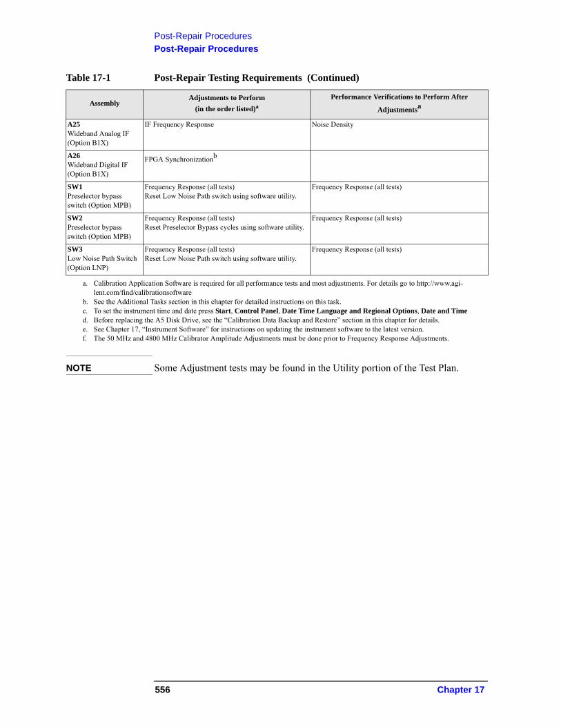
Post-Repair Procedures
Post-Repair Procedures
NOTE Some Adjustment tests may be found in the Utility portion of the Test Plan.
A25 Wideband Analog IF (Option B1X)
IF Frequency Response Noise Density
A26 Wideband Digital IF (Option B1X)
FPGA Synchronizationb
SW1 Preselector bypass switch (Option MPB)
Frequency Response (all tests)Reset Low Noise Path switch using software utility.
Frequency Response (all tests)
SW2 Preselector bypass switch (Option MPB)
Frequency Response (all tests)Reset Preselector Bypass cycles using software utility.
Frequency Response (all tests)
SW3 Low Noise Path Switch (Option LNP)
Frequency Response (all tests)Reset Low Noise Path switch using software utility.
Frequency Response (all tests)
a. Calibration Application Software is required for all performance tests and most adjustments. For details go to http://www.agi-lent.com/find/calibrationsoftware
b. See the Additional Tasks section in this chapter for detailed instructions on this task.c. To set the instrument time and date press Start, Control Panel, Date Time Language and Regional Options, Date and Timed. Before replacing the A5 Disk Drive, see the “Calibration Data Backup and Restore” section in this chapter for details.e. See Chapter 17, “Instrument Software” for instructions on updating the instrument software to the latest version.f. The 50 MHz and 4800 MHz Calibrator Amplitude Adjustments must be done prior to Frequency Response Adjustments.
Table 17-1 Post-Repair Testing Requirements (Continued)
AssemblyAdjustments to Perform
(in the order listed)a
Performance Verifications to Perform After
Adjustmentsa
556 Chapter 17
Post-Repair Procedures
Post-Repair Procedures
Additional Tasks
Calibration Data Backup and Restore
In order for the instrument being repaired to not need all of the instrument adjustments and performance verification tests to be run after the A5 Disk Drive is replaced the calibration data will need to be backed up onto an external drive prior to removing the existing disk drive.
NOTE While the backing up and restoring of the calibration data to the new disk drive will return the instrument performance to the state that it was prior to a repair this does not guarantee that all instrument performance parameters meet their specified values. A full instrument calibration would be required to verify this.
Data Backup
There are two different backup procedures that might need to be followed. Which backup procedure to be run will depend on whether the software will run or not.
If the Instrument Software Application Will Run
1. Connect a USB keyboard and mouse to two of the instrument rear panel USB ports
2. Connect a USB FLASH drive to one of the front panel USB port.
3. Press System, Alignments, Backup or Restore Align Data.
4. The Alignment Data Wizard window as shown in Figure 17-1 will appear.
Chapter 17 557
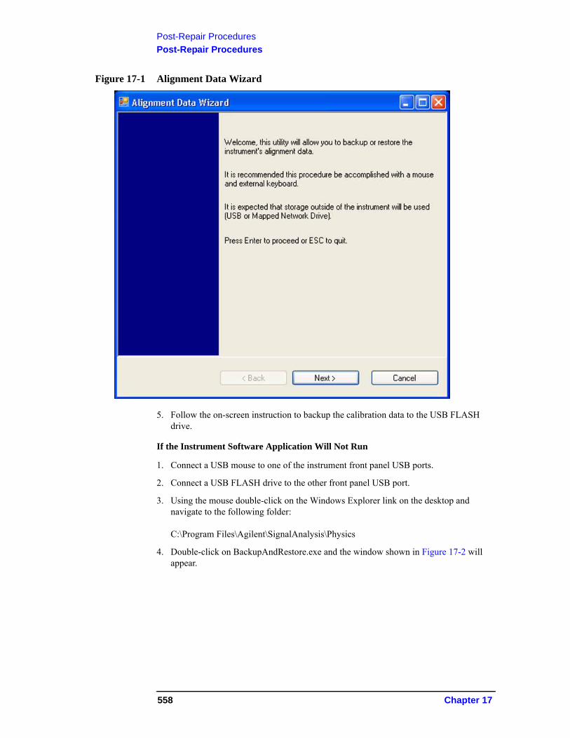
Post-Repair Procedures
Post-Repair Procedures
Figure 17-1 Alignment Data Wizard
5. Follow the on-screen instruction to backup the calibration data to the USB FLASH drive.
If the Instrument Software Application Will Not Run
1. Connect a USB mouse to one of the instrument front panel USB ports.
2. Connect a USB FLASH drive to the other front panel USB port.
3. Using the mouse double-click on the Windows Explorer link on the desktop and navigate to the following folder:
C:\Program Files\Agilent\SignalAnalysis\Physics
4. Double-click on BackupAndRestore.exe and the window shown in Figure 17-2 will appear.
558 Chapter 17
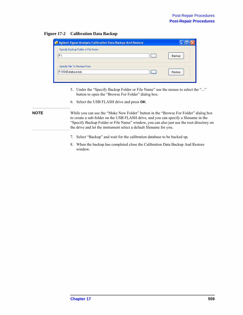
Post-Repair Procedures
Post-Repair Procedures
Figure 17-2 Calibration Data Backup
5. Under the “Specify Backup Folder or File Name” use the mouse to select the “...” button to open the “Browse For Folder” dialog box.
6. Select the USB FLASH drive and press OK.
NOTE While you can use the “Make New Folder” button in the “Browse For Folder” dialog box to create a sub-folder on the USB FLASH drive, and you can specify a filename in the “Specify Backup Folder or File Name” window, you can also just use the root directory on the drive and let the instrument select a default filename for you.
7. Select “Backup” and wait for the calibration database to be backed up.
8. When the backup has completed close the Calibration Data Backup And Restore window.
Chapter 17 559
Post-Repair Procedures
Post-Repair Procedures
Data Restore
1. Connect a USB mouse to one of the instrument front panel USB ports.
2. Locate the USB FLASH drive that was earlier used to backup the instrument calibration file and insert it into one of the instrument front panel USB ports.
3. Restore the instrument calibration data by pressing: System, Alignments, Backup or Restore Align Data... The Alignment Data Wizard window as shown in Figure 17-1 will appear.
4. Follow the on-screen instruction to restore the previously saved calibration data from the USB FLASH drive.
5. Cycle instrument power.
560 Chapter 17
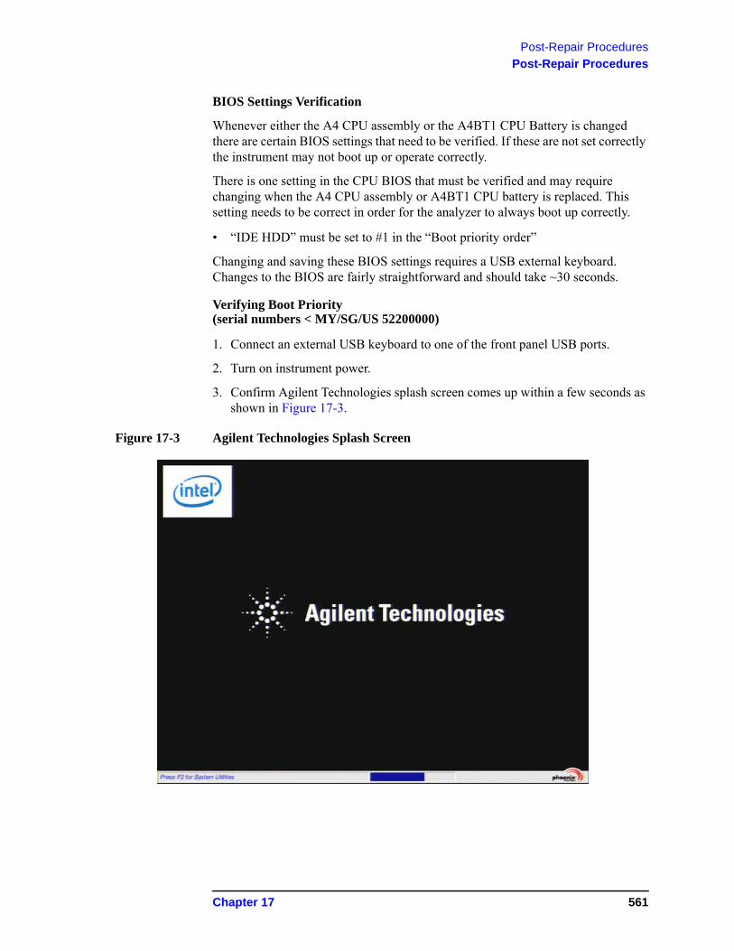
Post-Repair Procedures
Post-Repair Procedures
BIOS Settings Verification
Whenever either the A4 CPU assembly or the A4BT1 CPU Battery is changed there are certain BIOS settings that need to be verified. If these are not set correctly the instrument may not boot up or operate correctly.
There is one setting in the CPU BIOS that must be verified and may require changing when the A4 CPU assembly or A4BT1 CPU battery is replaced. This setting needs to be correct in order for the analyzer to always boot up correctly.
• “IDE HDD” must be set to #1 in the “Boot priority order”
Changing and saving these BIOS settings requires a USB external keyboard. Changes to the BIOS are fairly straightforward and should take ~30 seconds.
Verifying Boot Priority(serial numbers < MY/SG/US 52200000)
1. Connect an external USB keyboard to one of the front panel USB ports.
2. Turn on instrument power.
3. Confirm Agilent Technologies splash screen comes up within a few seconds as shown in Figure 17-3.
Figure 17-3 Agilent Technologies Splash Screen
Chapter 17 561
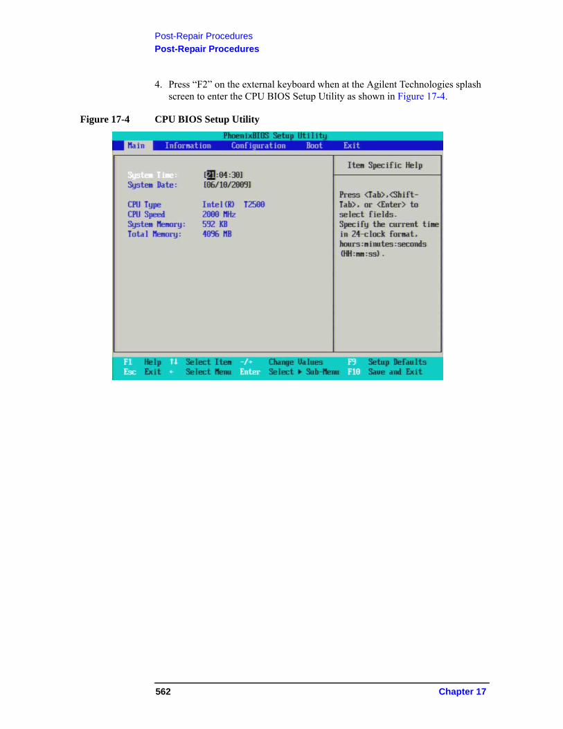
Post-Repair Procedures
Post-Repair Procedures
4. Press “F2” on the external keyboard when at the Agilent Technologies splash screen to enter the CPU BIOS Setup Utility as shown in Figure 17-4.
Figure 17-4 CPU BIOS Setup Utility
562 Chapter 17
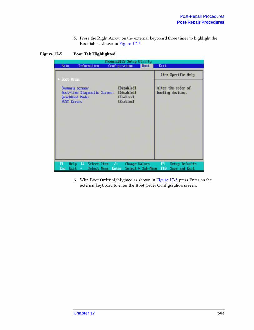
Post-Repair Procedures
Post-Repair Procedures
5. Press the Right Arrow on the external keyboard three times to highlight the Boot tab as shown in Figure 17-5.
Figure 17-5 Boot Tab Highlighted
6. With Boot Order highlighted as shown in Figure 17-5 press Enter on the external keyboard to enter the Boot Order Configuration screen.
Chapter 17 563
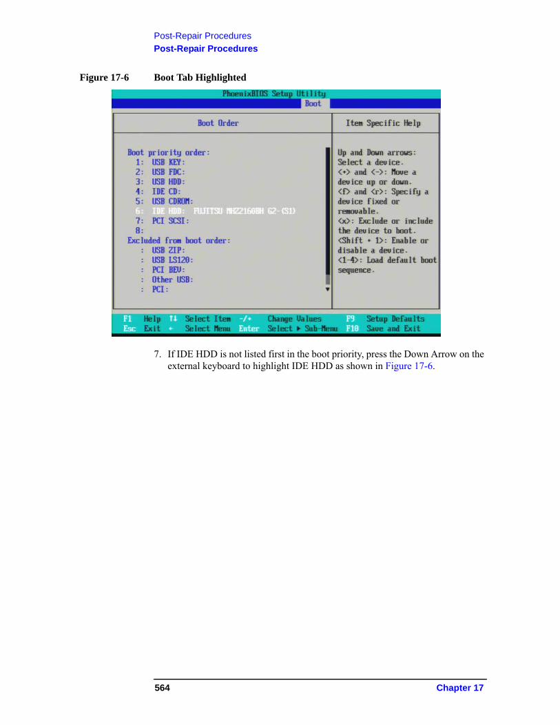
Post-Repair Procedures
Post-Repair Procedures
Figure 17-6 Boot Tab Highlighted
7. If IDE HDD is not listed first in the boot priority, press the Down Arrow on the external keyboard to highlight IDE HDD as shown in Figure 17-6.
564 Chapter 17
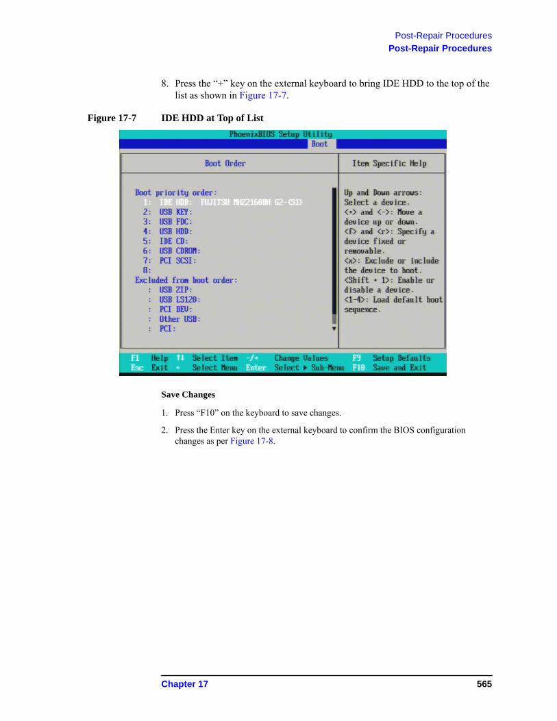
Post-Repair Procedures
Post-Repair Procedures
8. Press the “+” key on the external keyboard to bring IDE HDD to the top of the list as shown in Figure 17-7.
Figure 17-7 IDE HDD at Top of List
Save Changes
1. Press “F10” on the keyboard to save changes.
2. Press the Enter key on the external keyboard to confirm the BIOS configuration changes as per Figure 17-8.
Chapter 17 565
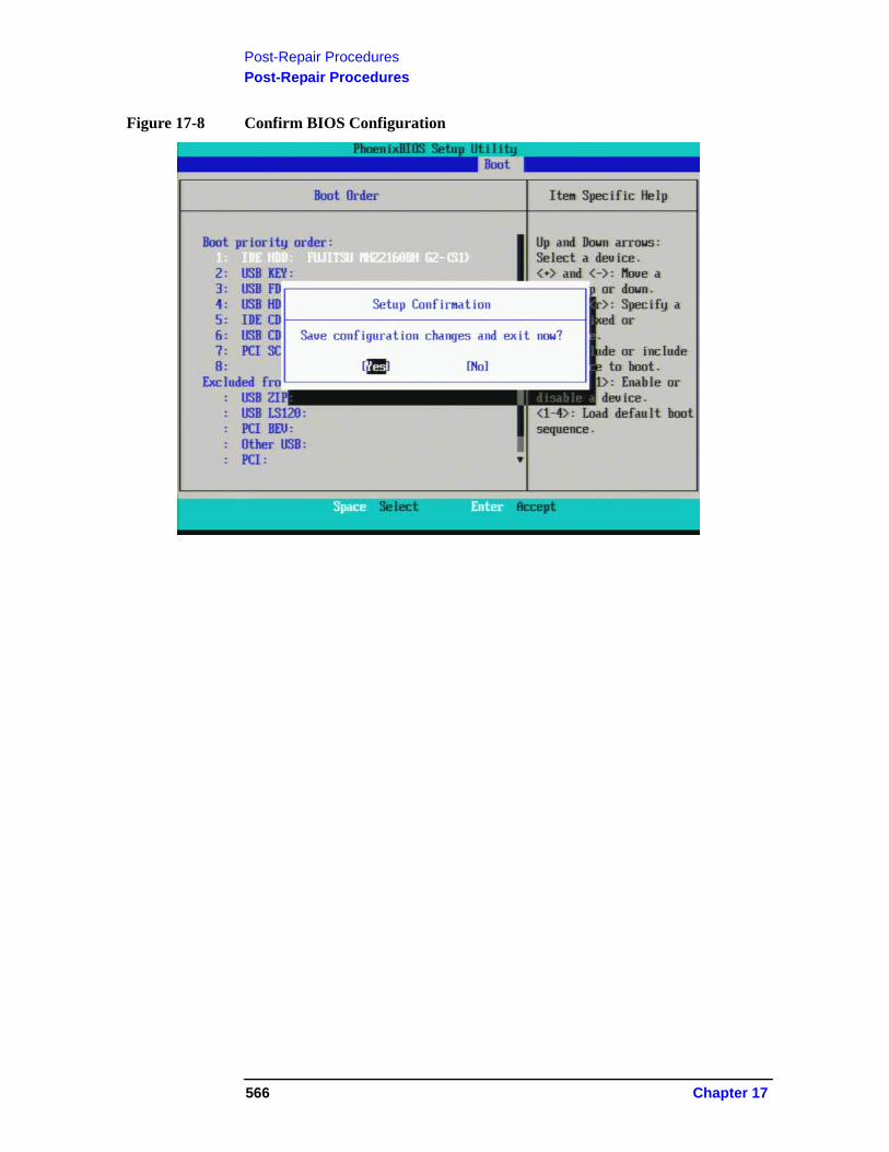
Post-Repair Procedures
Post-Repair Procedures
Figure 17-8 Confirm BIOS Configuration
566 Chapter 17
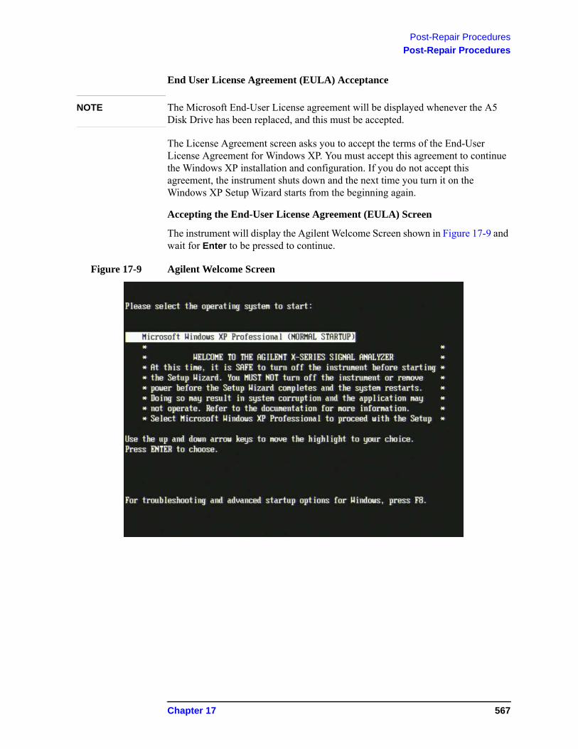
Post-Repair Procedures
Post-Repair Procedures
End User License Agreement (EULA) Acceptance
NOTE The Microsoft End-User License agreement will be displayed whenever the A5 Disk Drive has been replaced, and this must be accepted.
The License Agreement screen asks you to accept the terms of the End-User License Agreement for Windows XP. You must accept this agreement to continue the Windows XP installation and configuration. If you do not accept this agreement, the instrument shuts down and the next time you turn it on the Windows XP Setup Wizard starts from the beginning again.
Accepting the End-User License Agreement (EULA) Screen
The instrument will display the Agilent Welcome Screen shown in Figure 17-9 and wait for Enter to be pressed to continue.
Figure 17-9 Agilent Welcome Screen
Chapter 17 567
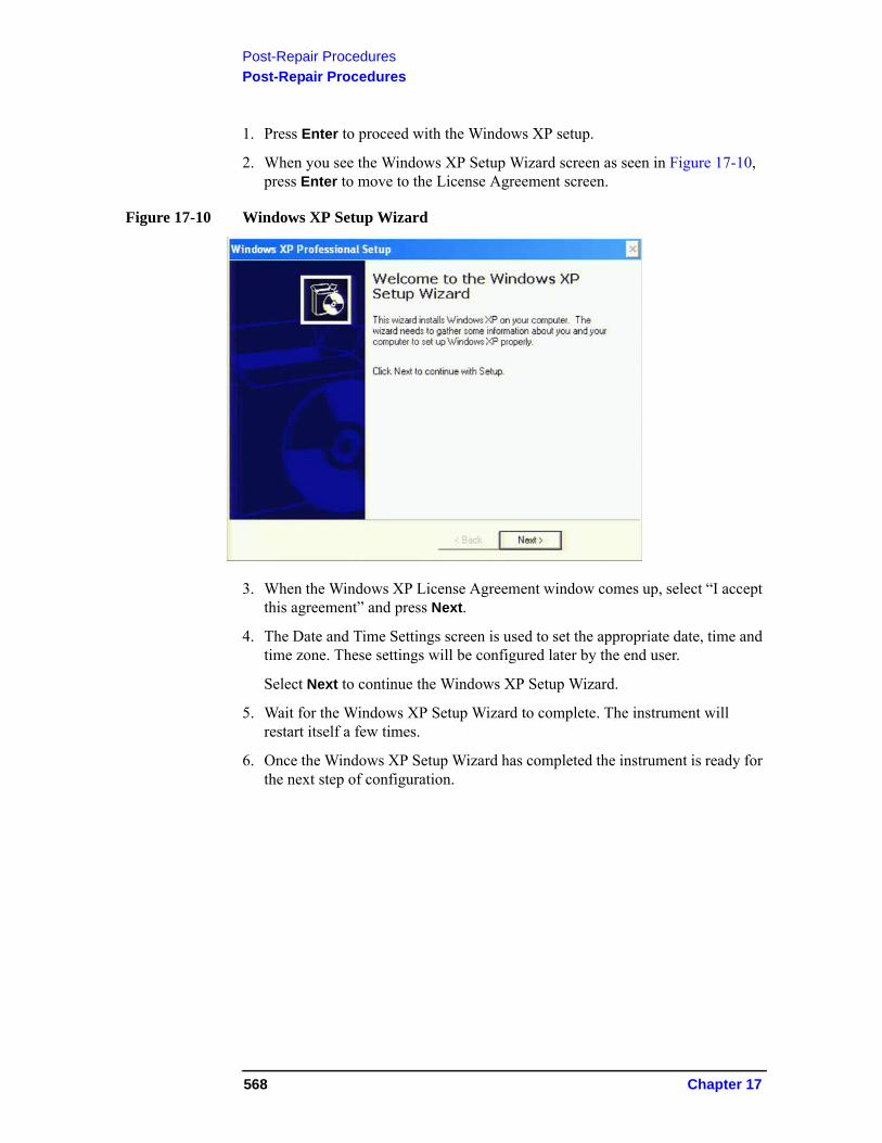
Post-Repair Procedures
Post-Repair Procedures
1. Press Enter to proceed with the Windows XP setup.
2. When you see the Windows XP Setup Wizard screen as seen in Figure 17-10, press Enter to move to the License Agreement screen.
Figure 17-10 Windows XP Setup Wizard
3. When the Windows XP License Agreement window comes up, select “I accept this agreement” and press Next.
4. The Date and Time Settings screen is used to set the appropriate date, time and time zone. These settings will be configured later by the end user.
Select Next to continue the Windows XP Setup Wizard.
5. Wait for the Windows XP Setup Wizard to complete. The instrument will restart itself a few times.
6. Once the Windows XP Setup Wizard has completed the instrument is ready for the next step of configuration.
568 Chapter 17
Post-Repair Procedures
Post-Repair Procedures
FPGA Synchronization
There is FPGA (Field-Programmable Gate Array) program code on many different assemblies inside of the instrument, and all of these must be of a compatible version with the instrument software revision. In order to ensure that this requirement is met when either an assembly is replaced that contains FPGA code on it, or if the A5 Disk Drive is replaced with a drive that has a different version of software than the previous drive, you will need to take certain steps to ensure that the instrument operates properly.
NOTE Even if an instrument appears to work properly when an assembly with FPGA code is replaced, that does not mean that the FPGA code is completely compatible with the software version installed in the instrument. There could be incompatibilities that will only be seen under certain measurement conditions.
Updating the Instrument FPGA Code
All instruments have a utility included in them that will update the FPGA code on all of the different assemblies in the instrument that have it. When this utility is run it will detect the assemblies that need to be updated and will update them to the correct revision.
NOTE Once you start the FPGA programming process you MUST NOT interrupt the process for any reason. This would include turning the instrument off or unplugging the power cord to the instrument. Doing so will result in an inoperative instrument, requiring the affected assembly to be replaced.
1. Close the instrument application software by pressing File, Exit, Enter using the front panel keys.
2. Connect a USB mouse to one of the instrument front panel USB ports.
3. Using the mouse, click Start, Log Off, Log Off.
4. Re-login as “administrator”. The default password is “agilent4u”. Click OK.
5. Using the mouse double-click on the Windows Explorer link on the desktop and navigate to the following folder:
C:\Program Files\Agilent\SignalAnalysis\Physics
6. In this folder find and execute the file named:
FPGA_Prog.bat
7. The FPGA Programming Utility will start and a window as shown in Figure 17-11 will appear.
Chapter 17 569
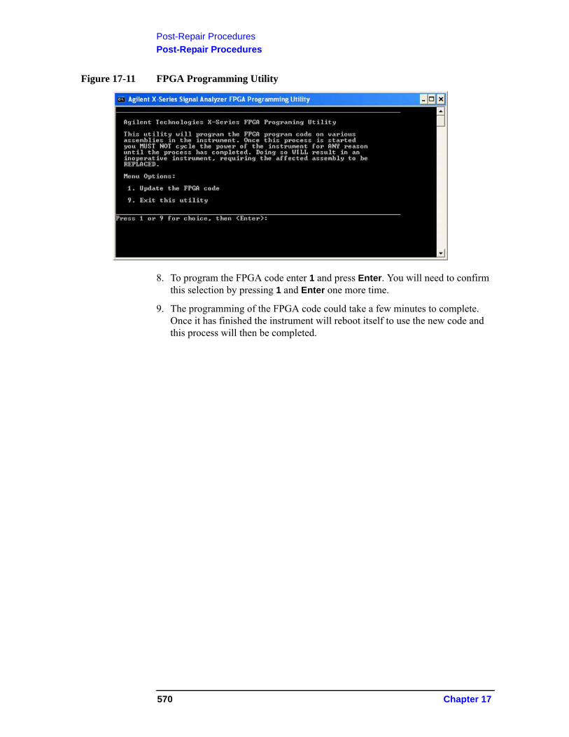
Post-Repair Procedures
Post-Repair Procedures
Figure 17-11 FPGA Programming Utility
8. To program the FPGA code enter 1 and press Enter. You will need to confirm this selection by pressing 1 and Enter one more time.
9. The programming of the FPGA code could take a few minutes to complete. Once it has finished the instrument will reboot itself to use the new code and this process will then be completed.
570 Chapter 17
Post-Repair Procedures
Post-Repair Procedures
Programming Model and Serial Numbers
Since the instrument model and serial numbers are stored only on the A7 Midplane board assembly, this information will be lost when this board assembly is replaced. Until the instrument model and serial numbers are restored the instrument application software will not allow any user measurements to be made, due to the fact that all previously installed license keys will not be accepted. However, the license files will not be automatically deleted. Once the model and serial numbers are restore the license files will then be recognized and accepted, returning the instrument to the capability that was available prior to the A7 Midplane board assembly replacement.
To program the model and serial numbers into a replacement A7 Midplane board assembly the N7814A Agilent X-Series Signal Analyzer Calibration Application Software will be required.
Information regarding N7814A Agilent X-Series Signal Analyzer Calibration Application Software can be found at:
http://www.agilent.com/find/calibrationsoftware
When the calibration software first detects the instrument it will recognize that it does not have a valid model and serial number and will prompt the user to enter the correct values.
NOTE Be very careful when entering the instrument serial number into the software, because once it has been written it can no longer be changed.
Since the instrument model and serial numbers are stored on the A7 Midplane board assembly, this should only be required when this assembly has been replaced with a new one.
Chapter 17 571

Post-Repair Procedures
Post-Repair Procedures
572 Chapter 17

18 Functional Tests
573
Functional Tests
Functional Test Versus Performance Verification
Functional Test Versus Performance Verification
Functional tests are tests of various instrument parameters that give a high degree of confidence that the analyzer is operating correctly. They are recommended as a check of analyzer operation for incoming inspection or after a repair. Measurement uncertainty analysis is not available for functional tests, and the analyzer is checked against limits that are wider than the published specifications. The functional tests are designed to test an analyzer operating within the temperature range defined by the analyzer specifications using a minimum set of test equipment. If a test does not pass, performance verification tests must be run to determine whether a problem exists.
Functional tests use a minimum set of test equipment to check a much smaller range of parameters (and a limited number of data points for each parameter) than do performance verification tests. Functional tests use limits that are wider than the published specifications; measurement uncertainty analysis is not available for functional tests.
NOTE If a functional test does not pass, you must run performance verification tests to determine whether a problem exists.
Performance verification tests span a wide range of instrument parameters and provide the highest level of confidence that the instrument conforms to published specifications. These tests can be time consuming and require extensive test equipment.
574 Chapter 18
Functional Tests
Before Performing a Functional Test
Before Performing a Functional Test
1. Ensure that you have the proper test equipment.
2. Switch on the unit under test (UUT) and let it warm up (in accordance with warm-up requirements in the instrument specifications).
3. Allow sufficient warm-up time for the required test equipment (refer to individual instrument documentation for warm-up specifications).
4. Ensure that the analyzer’s frequency reference is set to Internal:
a. Press the Input/Output, More, Freq Ref In keys.
b. If the Freq Ref In softkey does not show Internal, press the Freq Ref In softkey and select Internal.
5. Following instrument warm-up, perform the auto align routine:
Press System, Alignments, Align Now, All.
NOTE Functional test accuracy depends on the precision of the test equipment used. Ensure that all of the test equipment is calibrated before running a functional test.
Chapter 18 575
Functional Tests
Test Equipment
TEST EQUIPMENT
The table below summarizes the test equipment needed to perform all of the functional tests. Alternate equipment model numbers are given in case the recommended equipment is not available. If neither the recommended nor the alternative test equipment are available, substitute equipment that meets or exceeds the critical specifications listed.
Analyzer Option Item Critical Specifications
RecommendedAgilent Model
Alternate Agilent Model
Adapters
All 3.5 mm (f) to 3.5mm (f)(connector saver for source)
Frequency: 10 MHz to 26.5 GHz
VSWR: < 1.1:183059B
1250-1749
All BNC (f) to SMA (m) Frequency: 40 MHz 1250-1200
All Type N (f) to Type N (f) Frequency: 10 MHz to 18 GHz
VSWR: < 1.05:1
1250-1472 1250-0777
All Type N (m) to 3.5 mm (m)
Frequency: 10 MHz to 18 GHz
VSWR: < 1.1:1
1250-1743
All Type N (m) to 3.5 mm (f) Frequency: 10 MHz to 18 GHz
VSWR: < 1.1:1
1250-1744
All Type N (f) to 3.5 mm (f) Frequency: 10 MHz to 18 GHz
VSWR: < 1.1:1
1250-1745
All Type N (m) to BNC (f) Frequency: 10 MHz to 1 GHz
VSWR: < 1.05:1
1250-1476
Attenuators
All 10 dB Step Attenuator Frequency: 50 MHz
Range: 0 to 70 dB
8495A 8496A
All 10 dB Fixed Attenuator (2 required)
Frequency: 50 MHz
VSWR: < 1.2:1
8493C Option 010
8493A Option 010or
8493B Option 010
PreampOptions(Pxx)
30 dB Fixed Attenuator Accuracy: < 0.05 dB @ 50 MHz 11708A
Cables
All 3.5 mm (1 meter) Frequency: 10 MHz to 26.5 GHz
VSWR: < 1.4:1
Loss: < 2.0 dB
11500E 8120-4921
576 Chapter 18
Functional Tests
Test Equipment
543, 544, 550
2.4 mm (1 meter) Frequency: 10 MHz to 50 GHz
VSWR: < 1.55:1 at 50 GHz
Loss: < 6.0 dB at 50 GHz
8120-6164
All Cable, BNC (3 required)
120 cm (48 in.) BNC cable 10503A
BBA Cable, BNC 120 cm (48 in.) BNC cable
Flatness:(250 kHz to 40 MHz) < 0.5 dB
10503A
BBA Cable, BNC BNC (m)23 cm (9 in) max
10502A
Signal Source
All Synthesized Sweeper Frequency: 10 MHz to 50 GHza
Harmonic level: < − 40 dBcAmplitude range: 10 to − 20 dBmFrequency Accuracy: 0.02%
PSGb 83630B,83640B,83650B
BBA RF Signal Generator Frequency: 250 kHz to 40 MHzAmplitude: ~ − 10 dBmFlatness:< ± 0.75 dB
E4438C 33250A
Power Meter
All Power Meter Power Reference Accuracy: ±1.2%Compatible with power sensor
E4418B E4419B
All Power Sensor Frequency Range: 50 MHz to 3.66 GHz
Amplitude Range: −70 to –20 dBm
8481D 8487D8485D
503, 508, 513
Power Sensor Frequency Range: 50 MHz to 13.66 GHz
Amplitude Range: −30 to +20 dBm
8481A
526 Power Sensor Frequency Range: 50 MHz to 26.5 GHz
Amplitude Range: −30 to +20 dBm
8485A
543, 544, 550
Power Sensor Frequency Range: 50 MHz to 50 GHz
Amplitude Range: −30 to +20 dBm
8487A
P03 Low Power Sensor Frequency Range: 50 MHz to 3.6 GHz
Amplitude Range: –70 to –20 dBm
8481D 8485D8487D
Preamp other than P03
Low Power Sensor Frequency Range: 50 MHz to 50 GHzc
Amplitude Range: –70 to –20 dBm
8487D 8485Dc
Analyzer Option Item Critical Specifications
RecommendedAgilent Model
Alternate Agilent Model
Chapter 18 577
Functional Tests
Test Equipment
Miscellaneous Equipment
All Filter, 50 MHz Low Pass Cutoff Frequency: 50 MHz
Rejection at 65 MHz: > 40 dB
Rejection at 75 MHz: > 60 dB
Rejection at 80 MHz: > 60 dB
Frequency: 10 MHz to 26.5 GHz
0955-0306
543, 544, 550
Power Splitter, 2.4 mm Nominal Insertion Loss: 8.5 dB
Tracking Between Ports: < 0.4 dB
11667C
526 Power Splitter, 3.5 mm Nominal Insertion Loss: 6 dB
Tracking Between Ports: < 0.25 dB
11667B
503, 508, 513
Power Splitter Nominal Insertion Loss: 6 dB
Tracking Between Ports: < 0.25 dB
11667A 11667B
All Termination, 50 Ω Type N (m) Connector
Frequency: 30 Hz to 26.5 GHz
909A Option 012
BBA Termination, 50 Ω BNC (m) Connector
Frequency: 250 kHz to 40 MHz
11593A
a. Maximum frequency equal to or greater than the maximum frequency of the PXA.b. PSG model numbers: E8244A, E8254A, E8247C Option 520, E8247C Option H31 or 540,
E8257D Option 520, E8257D Option 550, E8257D Option 567, E8267D Option 544.c. Maximum frequency equal to or greater than the maximum frequency of the preamplifier
option.
Analyzer Option Item Critical Specifications
RecommendedAgilent Model
Alternate Agilent Model
578 Chapter 18
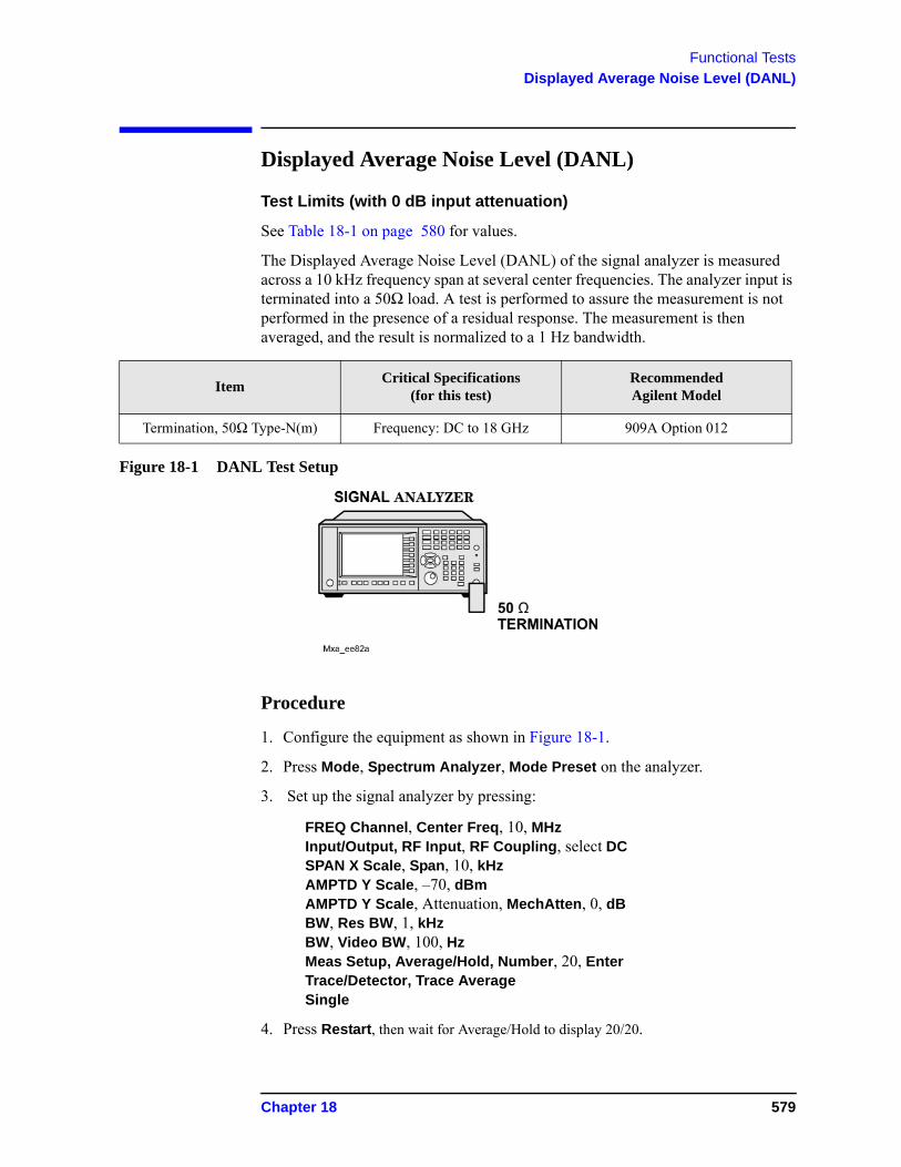
Functional Tests
Displayed Average Noise Level (DANL)
Displayed Average Noise Level (DANL)
Test Limits (with 0 dB input attenuation)
See Table 18-1 on page 580 for values.
The Displayed Average Noise Level (DANL) of the signal analyzer is measured across a 10 kHz frequency span at several center frequencies. The analyzer input is terminated into a 50Ω load. A test is performed to assure the measurement is not performed in the presence of a residual response. The measurement is then averaged, and the result is normalized to a 1 Hz bandwidth.
Figure 18-1 DANL Test Setup
Procedure
1. Configure the equipment as shown in Figure 18-1.
2. Press Mode, Spectrum Analyzer, Mode Preset on the analyzer.
3. Set up the signal analyzer by pressing:
FREQ Channel, Center Freq, 10, MHzInput/Output, RF Input, RF Coupling, select DCSPAN X Scale, Span, 10, kHzAMPTD Y Scale, –70, dBmAMPTD Y Scale, Attenuation, MechAtten, 0, dBBW, Res BW, 1, kHzBW, Video BW, 100, HzMeas Setup, Average/Hold, Number, 20, EnterTrace/Detector, Trace AverageSingle
4. Press Restart, then wait for Average/Hold to display 20/20.
ItemCritical Specifications
(for this test)RecommendedAgilent Model
Termination, 50Ω Type-N(m) Frequency: DC to 18 GHz 909A Option 012
Chapter 18 579
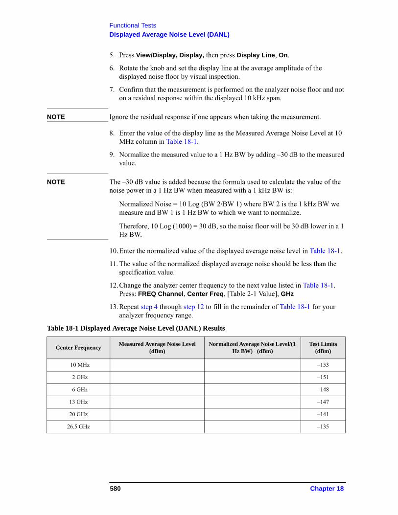
Functional Tests
Displayed Average Noise Level (DANL)
5. Press View/Display, Display, then press Display Line, On.
6. Rotate the knob and set the display line at the average amplitude of the displayed noise floor by visual inspection.
7. Confirm that the measurement is performed on the analyzer noise floor and not on a residual response within the displayed 10 kHz span.
NOTE Ignore the residual response if one appears when taking the measurement.
8. Enter the value of the display line as the Measured Average Noise Level at 10 MHz column in Table 18-1.
9. Normalize the measured value to a 1 Hz BW by adding –30 dB to the measured value.
NOTE The –30 dB value is added because the formula used to calculate the value of the noise power in a 1 Hz BW when measured with a 1 kHz BW is:
Normalized Noise = 10 Log (BW 2/BW 1) where BW 2 is the 1 kHz BW we measure and BW 1 is 1 Hz BW to which we want to normalize.
Therefore, 10 Log (1000) = 30 dB, so the noise floor will be 30 dB lower in a 1 Hz BW.
10.Enter the normalized value of the displayed average noise level in Table 18-1.
11. The value of the normalized displayed average noise should be less than the specification value.
12.Change the analyzer center frequency to the next value listed in Table 18-1. Press: FREQ Channel, Center Freq, [Table 2-1 Value], GHz
13.Repeat step 4 through step 12 to fill in the remainder of Table 18-1 for your analyzer frequency range.
Table 18-1 Displayed Average Noise Level (DANL) Results
Center FrequencyMeasured Average Noise Level
(dBm)Normalized Average Noise Level/(1
Hz BW) (dBm)Test Limits
(dBm)
10 MHz –153
2 GHz –151
6 GHz –148
13 GHz –147
20 GHz –141
26.5 GHz –135
580 Chapter 18
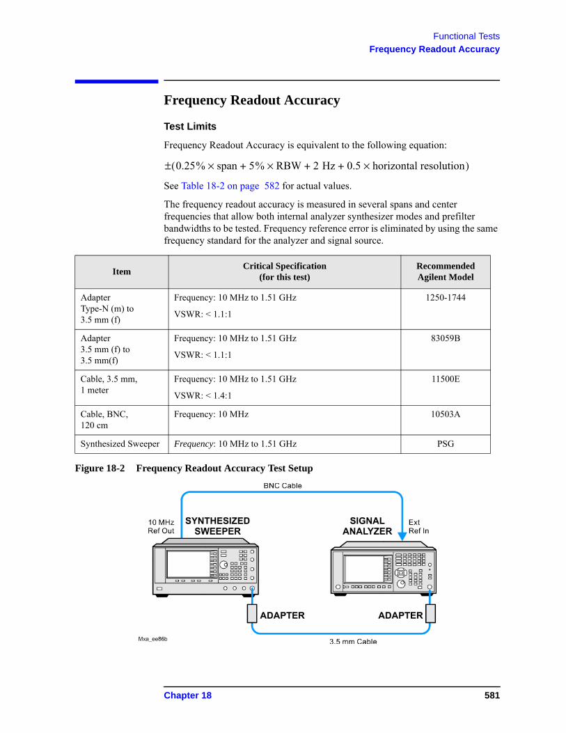
Functional Tests
Frequency Readout Accuracy
Frequency Readout Accuracy
Test Limits
Frequency Readout Accuracy is equivalent to the following equation:
See Table 18-2 on page 582 for actual values.
The frequency readout accuracy is measured in several spans and center frequencies that allow both internal analyzer synthesizer modes and prefilter bandwidths to be tested. Frequency reference error is eliminated by using the same frequency standard for the analyzer and signal source.
Figure 18-2 Frequency Readout Accuracy Test Setup
0.25% span 5% RBW 2 Hz 0.5 horizontal resolution×+ +×+×( )±
ItemCritical Specification
(for this test)Recommended Agilent Model
AdapterType-N (m) to 3.5 mm (f)
Frequency: 10 MHz to 1.51 GHz
VSWR: < 1.1:1
1250-1744
Adapter3.5 mm (f) to 3.5 mm(f)
Frequency: 10 MHz to 1.51 GHz
VSWR: < 1.1:1
83059B
Cable, 3.5 mm, 1 meter
Frequency: 10 MHz to 1.51 GHz
VSWR: < 1.4:1
11500E
Cable, BNC, 120 cm
Frequency: 10 MHz 10503A
Synthesized Sweeper Frequency: 10 MHz to 1.51 GHz PSG
Chapter 18 581
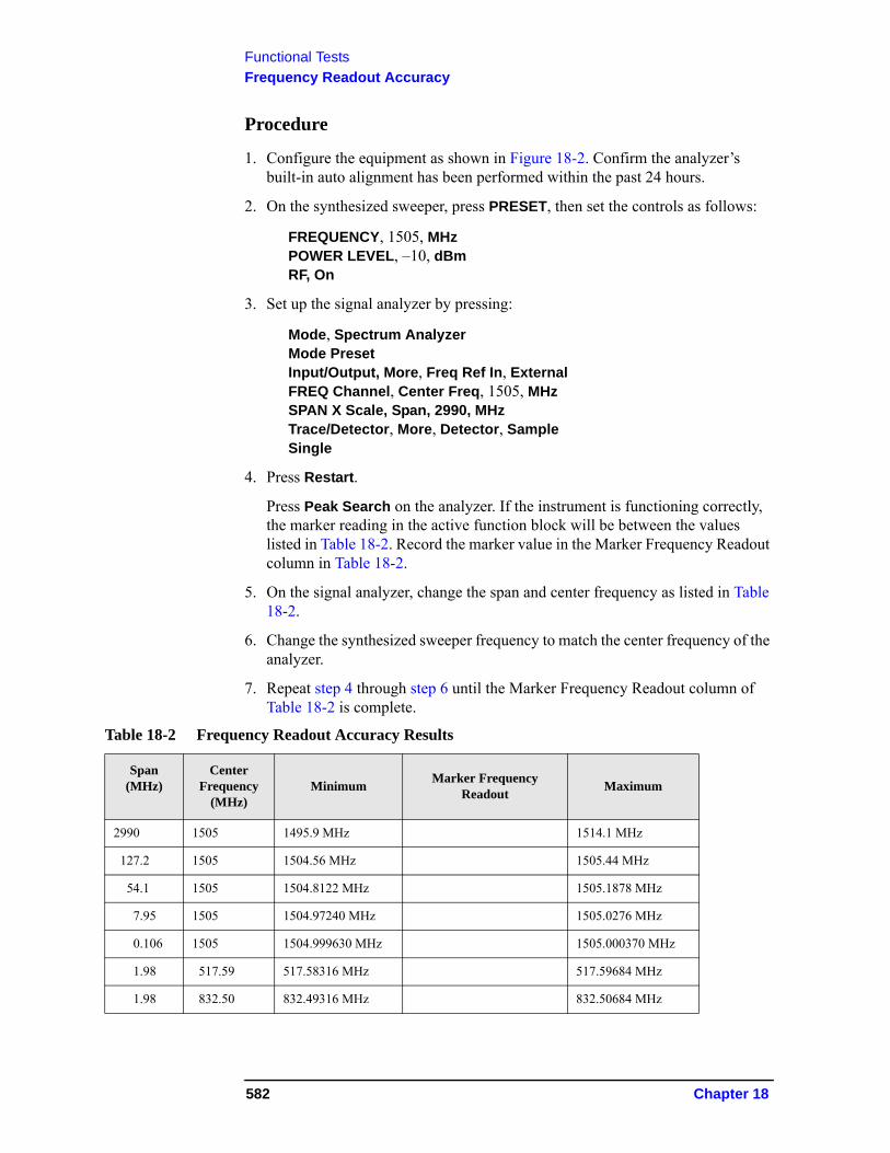
Functional Tests
Frequency Readout Accuracy
Procedure
1. Configure the equipment as shown in Figure 18-2. Confirm the analyzer’s built-in auto alignment has been performed within the past 24 hours.
2. On the synthesized sweeper, press PRESET, then set the controls as follows:
FREQUENCY, 1505, MHzPOWER LEVEL, –10, dBmRF, On
3. Set up the signal analyzer by pressing:
Mode, Spectrum AnalyzerMode PresetInput/Output, More, Freq Ref In, ExternalFREQ Channel, Center Freq, 1505, MHzSPAN X Scale, Span, 2990, MHzTrace/Detector, More, Detector, SampleSingle
4. Press Restart.
Press Peak Search on the analyzer. If the instrument is functioning correctly, the marker reading in the active function block will be between the values listed in Table 18-2. Record the marker value in the Marker Frequency Readout column in Table 18-2.
5. On the signal analyzer, change the span and center frequency as listed in Table 18-2.
6. Change the synthesized sweeper frequency to match the center frequency of the analyzer.
7. Repeat step 4 through step 6 until the Marker Frequency Readout column of Table 18-2 is complete.
Table 18-2 Frequency Readout Accuracy Results
Span(MHz)
CenterFrequency
(MHz)Minimum
Marker Frequency Readout
Maximum
2990 1505 1495.9 MHz 1514.1 MHz
127.2 1505 1504.56 MHz 1505.44 MHz
54.1 1505 1504.8122 MHz 1505.1878 MHz
7.95 1505 1504.97240 MHz 1505.0276 MHz
0.106 1505 1504.999630 MHz 1505.000370 MHz
1.98 517.59 517.58316 MHz 517.59684 MHz
1.98 832.50 832.49316 MHz 832.50684 MHz
582 Chapter 18
Functional Tests
Second Harmonic Distortion (SHD)
Second Harmonic Distortion (SHD)
Test Limits
This test checks the second harmonic distortion of the signal analyzer by tuning to twice the input frequency and examining the level of the distortion product. A low pass filter is inserted between the source and the signal analyzer to prevent the source second harmonic from artificially raising the second harmonic product displayed on the analyzer.
Applied Frequency Mixer Levela
a. Mixer Level = Input Level - RF Attenuation
Distortion
40 MHz –15 dBm < –60 dBc
ItemCritical Specifications
(for this test)Recommended Agilent Model
AdapterType-N (m) to BNC (f)
Frequency: 10 MHz to 80 MHz
VSWR: < 1.05:1
1250-1476
AdapterBNC (f) to SMA (m)
Frequency: 40 to 80 MHz 1250-1200
Adapter3.5 mm (f) to 3.5 mm (f)
Frequency: 10 MHz to 80 MHz
VSWR: < 1.1:1
83059B
Cable, BNC 120 cm (2 required)
Frequency: 10 to 40 MHz 10503A
Filter, 50 MHz Low Pass
Cutoff Frequency: 50 MHzRejection at 65 MHz: > 40 dBRejection at 75 MHz: > 60 dB
0955-0306
Synthesized Sweeper Frequency: 50 MHzSpectral Purity: Better than –30 dBc
PSG
Chapter 18 583
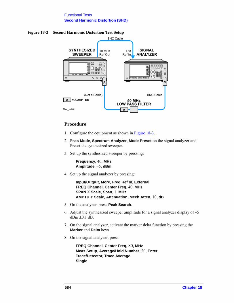
Functional Tests
Second Harmonic Distortion (SHD)
Figure 18-3 Second Harmonic Distortion Test Setup
Procedure
1. Configure the equipment as shown in Figure 18-3.
2. Press Mode, Spectrum Analyzer, Mode Preset on the signal analyzer and Preset the synthesized sweeper.
3. Set up the synthesized sweeper by pressing:
Frequency, 40, MHzAmplitude, –5, dBm
4. Set up the signal analyzer by pressing:
Input/Output, More, Freq Ref In, ExternalFREQ Channel, Center Freq, 40, MHzSPAN X Scale, Span, 1, MHzAMPTD Y Scale, Attenuation, Mech Atten, 10, dB
5. On the analyzer, press Peak Search.
6. Adjust the synthesized sweeper amplitude for a signal analyzer display of –5 dBm ±0.1 dB.
7. On the signal analyzer, activate the marker delta function by pressing the Marker and Delta keys.
8. On the signal analyzer, press:
FREQ Channel, Center Freq, 80, MHzMeas Setup, Average/Hold Number, 20, EnterTrace/Detector, Trace AverageSingle
584 Chapter 18
Functional Tests
Second Harmonic Distortion (SHD)
9. Press Peak Search. Enter the displayed value under the Measured Second Harmonic Distortion (dBc) heading in Table 18-3.
Table 18-3 Second Harmonic Distortion Results
Applied Frequency (MHz)
Measured Second Harmonic Distortion (dBc)
Mixer Level(dBm)
Specification (dBc)
40 –15 –60
Chapter 18 585
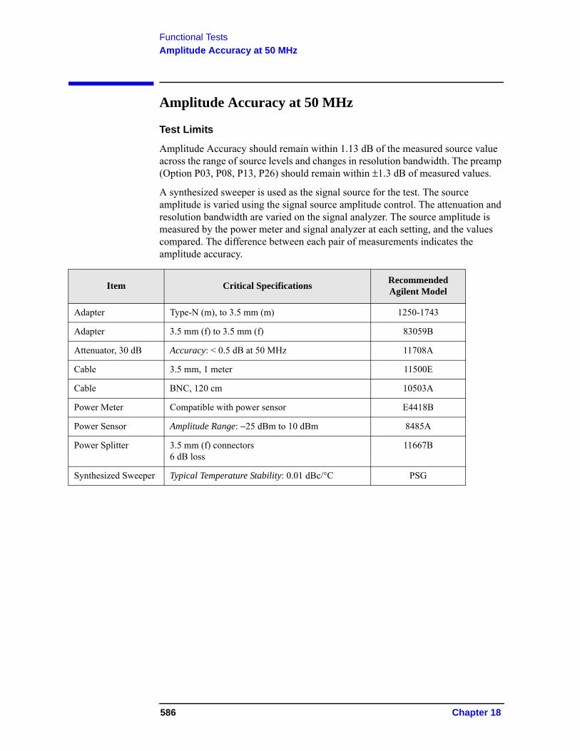
Functional Tests
Amplitude Accuracy at 50 MHz
Amplitude Accuracy at 50 MHz
Test Limits
Amplitude Accuracy should remain within 1.13 dB of the measured source value across the range of source levels and changes in resolution bandwidth. The preamp (Option P03, P08, P13, P26) should remain within ±1.3 dB of measured values.
A synthesized sweeper is used as the signal source for the test. The source amplitude is varied using the signal source amplitude control. The attenuation and resolution bandwidth are varied on the signal analyzer. The source amplitude is measured by the power meter and signal analyzer at each setting, and the values compared. The difference between each pair of measurements indicates the amplitude accuracy.
Item Critical SpecificationsRecommended Agilent Model
Adapter Type-N (m), to 3.5 mm (m) 1250-1743
Adapter 3.5 mm (f) to 3.5 mm (f) 83059B
Attenuator, 30 dB Accuracy: < 0.5 dB at 50 MHz 11708A
Cable 3.5 mm, 1 meter 11500E
Cable BNC, 120 cm 10503A
Power Meter Compatible with power sensor E4418B
Power Sensor Amplitude Range: −25 dBm to 10 dBm 8485A
Power Splitter 3.5 mm (f) connectors6 dB loss
11667B
Synthesized Sweeper Typical Temperature Stability: 0.01 dBc/°C PSG
586 Chapter 18
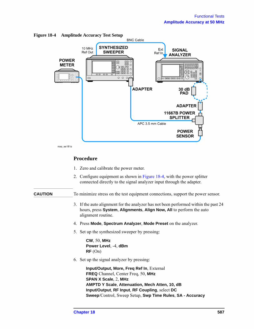
Functional Tests
Amplitude Accuracy at 50 MHz
Figure 18-4 Amplitude Accuracy Test Setup
Procedure
1. Zero and calibrate the power meter.
2. Configure equipment as shown in Figure 18-4, with the power splitter connected directly to the signal analyzer input through the adapter.
CAUTION To minimize stress on the test equipment connections, support the power sensor.
3. If the auto alignment for the analyzer has not been performed within the past 24 hours, press System, Alignments, Align Now, All to perform the auto alignment routine.
4. Press Mode, Spectrum Analyzer, Mode Preset on the analyzer.
5. Set up the synthesized sweeper by pressing:
CW, 50, MHzPower Level, -4, dBmRF (On)
6. Set up the signal analyzer by pressing:
Input/Output, More, Freq Ref In, ExternalFREQ Channel, Center Freq, 50, MHzSPAN X Scale, 2, MHzAMPTD Y Scale, Attenuation, Mech Atten, 10, dBInput/Output, RF Input, RF Coupling, select DCSweep/Control, Sweep Setup, Swp Time Rules, SA - Accuracy
Chapter 18 587
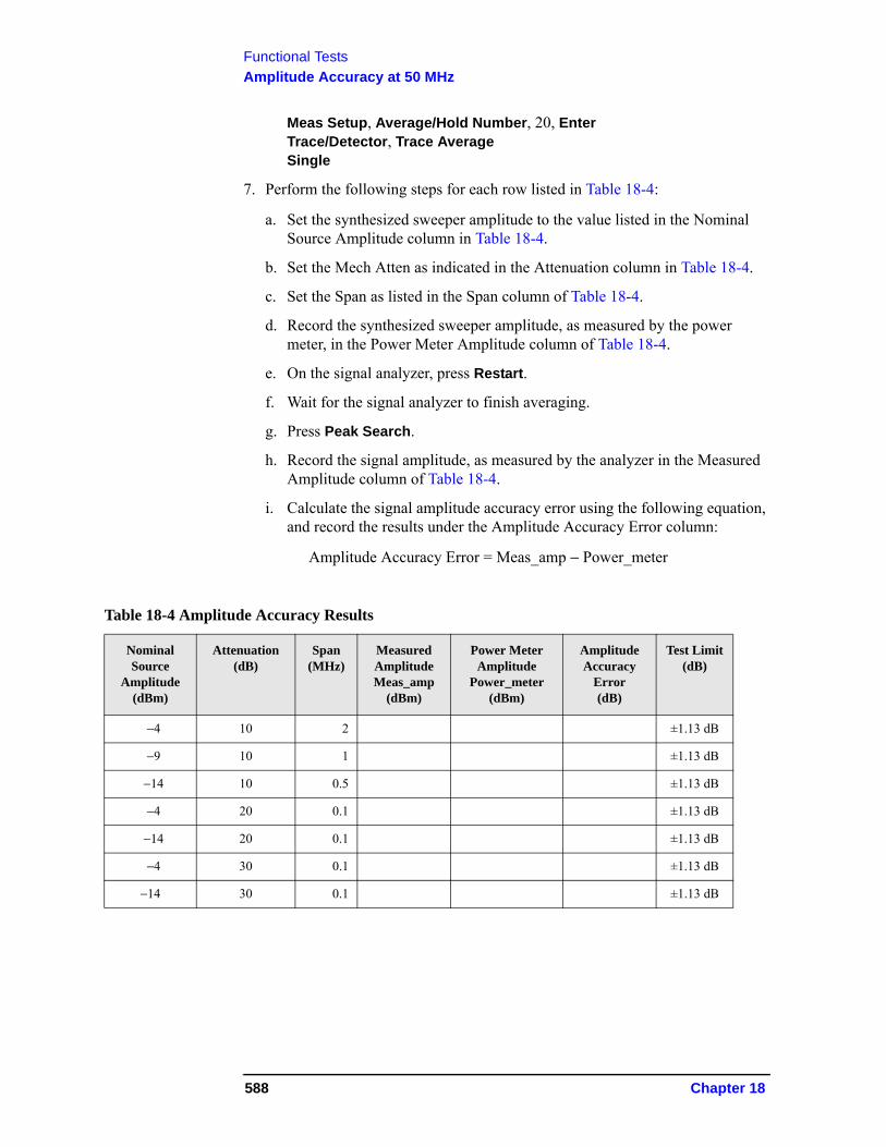
Functional Tests
Amplitude Accuracy at 50 MHz
Meas Setup, Average/Hold Number, 20, EnterTrace/Detector, Trace AverageSingle
7. Perform the following steps for each row listed in Table 18-4:
a. Set the synthesized sweeper amplitude to the value listed in the Nominal Source Amplitude column in Table 18-4.
b. Set the Mech Atten as indicated in the Attenuation column in Table 18-4.
c. Set the Span as listed in the Span column of Table 18-4.
d. Record the synthesized sweeper amplitude, as measured by the power meter, in the Power Meter Amplitude column of Table 18-4.
e. On the signal analyzer, press Restart.
f. Wait for the signal analyzer to finish averaging.
g. Press Peak Search.
h. Record the signal amplitude, as measured by the analyzer in the Measured Amplitude column of Table 18-4.
i. Calculate the signal amplitude accuracy error using the following equation, and record the results under the Amplitude Accuracy Error column:
Amplitude Accuracy Error = Meas_amp − Power_meter
Table 18-4 Amplitude Accuracy Results
NominalSource
Amplitude(dBm)
Attenuation(dB)
Span (MHz)
MeasuredAmplitudeMeas_amp
(dBm)
Power MeterAmplitude
Power_meter(dBm)
AmplitudeAccuracy
Error(dB)
Test Limit(dB)
−4 10 2 ±1.13 dB
−9 10 1 ±1.13 dB
−14 10 0.5 ±1.13 dB
−4 20 0.1 ±1.13 dB
−14 20 0.1 ±1.13 dB
−4 30 0.1 ±1.13 dB
−14 30 0.1 ±1.13 dB
588 Chapter 18
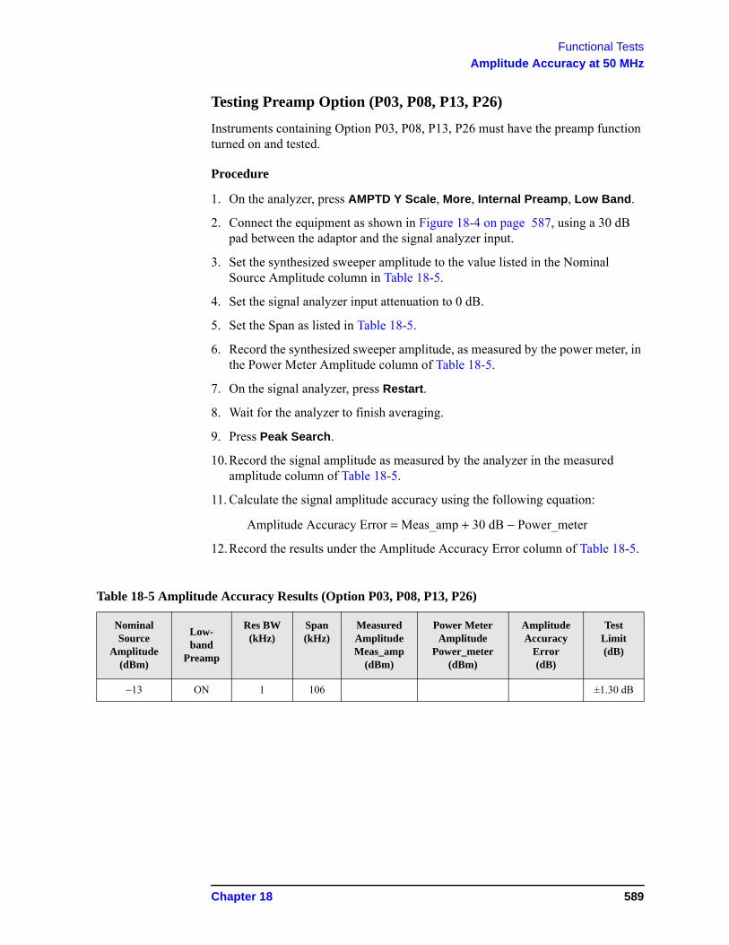
Functional Tests
Amplitude Accuracy at 50 MHz
Testing Preamp Option (P03, P08, P13, P26)
Instruments containing Option P03, P08, P13, P26 must have the preamp function turned on and tested.
Procedure
1. On the analyzer, press AMPTD Y Scale, More, Internal Preamp, Low Band.
2. Connect the equipment as shown in Figure 18-4 on page 587, using a 30 dB pad between the adaptor and the signal analyzer input.
3. Set the synthesized sweeper amplitude to the value listed in the Nominal Source Amplitude column in Table 18-5.
4. Set the signal analyzer input attenuation to 0 dB.
5. Set the Span as listed in Table 18-5.
6. Record the synthesized sweeper amplitude, as measured by the power meter, in the Power Meter Amplitude column of Table 18-5.
7. On the signal analyzer, press Restart.
8. Wait for the analyzer to finish averaging.
9. Press Peak Search.
10.Record the signal amplitude as measured by the analyzer in the measured amplitude column of Table 18-5.
11. Calculate the signal amplitude accuracy using the following equation:
Amplitude Accuracy Error = Meas_amp + 30 dB − Power_meter
12.Record the results under the Amplitude Accuracy Error column of Table 18-5.
Table 18-5 Amplitude Accuracy Results (Option P03, P08, P13, P26)
NominalSource
Amplitude(dBm)
Low- band
Preamp
Res BW (kHz)
Span (kHz)
MeasuredAmplitudeMeas_amp
(dBm)
Power MeterAmplitude
Power_meter(dBm)
AmplitudeAccuracy
Error(dB)
Test Limit(dB)
−13 ON 1 106 ±1.30 dB
Chapter 18 589
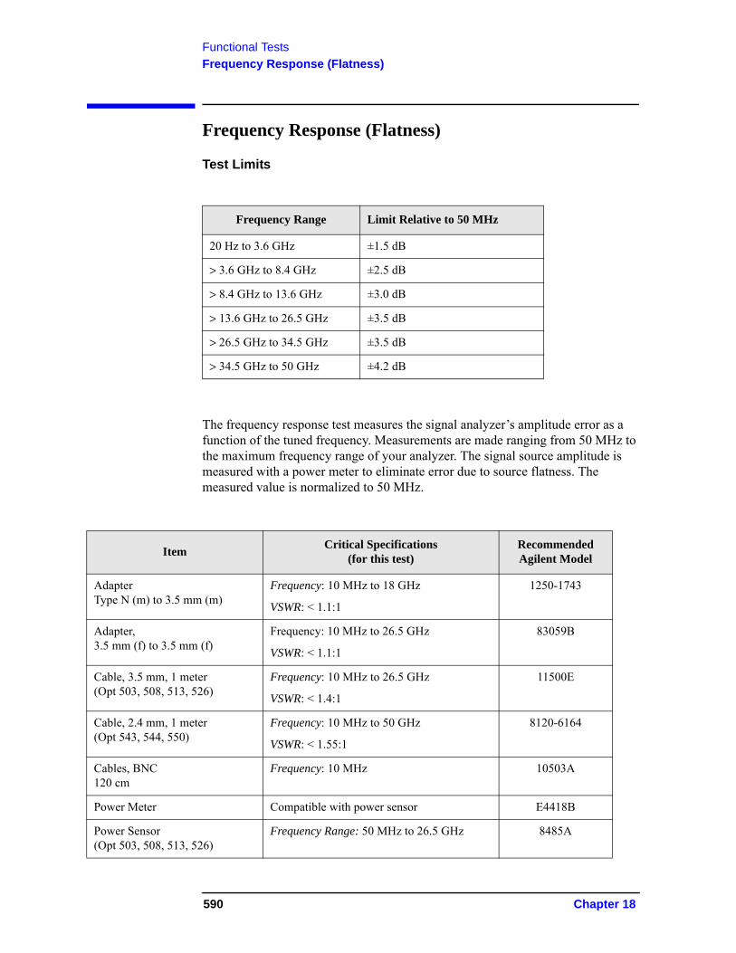
Functional Tests
Frequency Response (Flatness)
Frequency Response (Flatness)
Test Limits
The frequency response test measures the signal analyzer’s amplitude error as a function of the tuned frequency. Measurements are made ranging from 50 MHz to the maximum frequency range of your analyzer. The signal source amplitude is measured with a power meter to eliminate error due to source flatness. The measured value is normalized to 50 MHz.
Frequency Range Limit Relative to 50 MHz
20 Hz to 3.6 GHz ±1.5 dB
> 3.6 GHz to 8.4 GHz ±2.5 dB
> 8.4 GHz to 13.6 GHz ±3.0 dB
> 13.6 GHz to 26.5 GHz ±3.5 dB
> 26.5 GHz to 34.5 GHz ±3.5 dB
> 34.5 GHz to 50 GHz ±4.2 dB
ItemCritical Specifications
(for this test)Recommended Agilent Model
AdapterType N (m) to 3.5 mm (m)
Frequency: 10 MHz to 18 GHz
VSWR: < 1.1:1
1250-1743
Adapter,3.5 mm (f) to 3.5 mm (f)
Frequency: 10 MHz to 26.5 GHz
VSWR: < 1.1:1
83059B
Cable, 3.5 mm, 1 meter(Opt 503, 508, 513, 526)
Frequency: 10 MHz to 26.5 GHz
VSWR: < 1.4:1
11500E
Cable, 2.4 mm, 1 meter(Opt 543, 544, 550)
Frequency: 10 MHz to 50 GHz
VSWR: < 1.55:1
8120-6164
Cables, BNC 120 cm
Frequency: 10 MHz 10503A
Power Meter Compatible with power sensor E4418B
Power Sensor(Opt 503, 508, 513, 526)
Frequency Range: 50 MHz to 26.5 GHz 8485A
590 Chapter 18
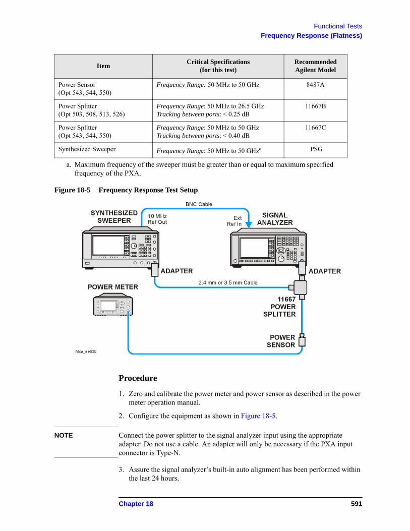
Functional Tests
Frequency Response (Flatness)
Figure 18-5 Frequency Response Test Setup
Procedure
1. Zero and calibrate the power meter and power sensor as described in the power meter operation manual.
2. Configure the equipment as shown in Figure 18-5.
NOTE Connect the power splitter to the signal analyzer input using the appropriate adapter. Do not use a cable. An adapter will only be necessary if the PXA input connector is Type-N.
3. Assure the signal analyzer’s built-in auto alignment has been performed within the last 24 hours.
Power Sensor(Opt 543, 544, 550)
Frequency Range: 50 MHz to 50 GHz 8487A
Power Splitter(Opt 503, 508, 513, 526)
Frequency Range: 50 MHz to 26.5 GHz Tracking between ports: < 0.25 dB
11667B
Power Splitter(Opt 543, 544, 550)
Frequency Range: 50 MHz to 50 GHz Tracking between ports: < 0.40 dB
11667C
Synthesized Sweeper Frequency Range: 50 MHz to 50 GHza PSG
a. Maximum frequency of the sweeper must be greater than or equal to maximum specified frequency of the PXA.
ItemCritical Specifications
(for this test)Recommended Agilent Model
Chapter 18 591
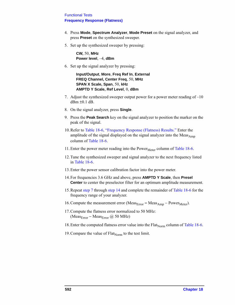
Functional Tests
Frequency Response (Flatness)
4. Press Mode, Spectrum Analyzer, Mode Preset on the signal analyzer, and press Preset on the synthesized sweeper.
5. Set up the synthesized sweeper by pressing:
CW, 50, MHzPower level, –4, dBm
6. Set up the signal analyzer by pressing:
Input/Output, More, Freq Ref In, ExternalFREQ Channel, Center Freq, 50, MHzSPAN X Scale, Span, 50, kHzAMPTD Y Scale, Ref Level, 0, dBm
7. Adjust the synthesized sweeper output power for a power meter reading of –10 dBm ±0.1 dB.
8. On the signal analyzer, press Single.
9. Press the Peak Search key on the signal analyzer to position the marker on the peak of the signal.
10.Refer to Table 18-6, “Frequency Response (Flatness) Results.” Enter the amplitude of the signal displayed on the signal analyzer into the MeasAmp column of Table 18-6.
11. Enter the power meter reading into the PowerMeter column of Table 18-6.
12.Tune the synthesized sweeper and signal analyzer to the next frequency listed in Table 18-6.
13.Enter the power sensor calibration factor into the power meter.
14.For frequencies 3.6 GHz and above, press AMPTD Y Scale, then Presel Center to center the preselector filter for an optimum amplitude measurement.
15.Repeat step 7 through step 14 and complete the remainder of Table 18-6 for the frequency range of your analyzer.
16.Compute the measurement error (MeasError = MeasAmp − PowerMeter).
17.Compute the flatness error normalized to 50 MHz:(MeasError − MeasError @ 50 MHz)
18.Enter the computed flatness error value into the FlatNorm column of Table 18-6.
19.Compare the value of FlatNorm to the test limit.
592 Chapter 18
Functional Tests
Frequency Response (Flatness)
Table 18-6 Frequency Response (Flatness) Results
CenterFrequency
Analyzer Amplitude
Measamp
Power Meter Measurement
Powermeter
Meas Error
Measerror
Flatness Normalizedto 50 MHzFlatNorm
Flatness ErrorTest Limits
(dB)
50 MHz 0 Ref
1 GHz ±1.5 dB
2 GHz 1.5 dB
3 GHz ±1.5 dB
3.5 GHz ±1.5 dB
4 GHz ±2.5 dB
6 GHz ±2.5 dB
8 GHz ±2.5 dB
9 GHz ±3.0 dB
11 GHz ±3.0 dB
13 GHz ±3.0 dB
14 GHz ±3.5 dB
17 GHz ±3.5 dB
20 GHz ±3.5 dB
23 GHz ±3.5 dB
26 GHz ±3.5 dB
29 GHz ±3.5 dB
32 GHz ±3.5 dB
35 GHz ±4.2 dB
38 GHz ±4.2 dB
41 GHz ±4.2 dB
42.5 GHz ±4.2 dB
43.5 GHz ±4.2 dB
46.5 GHz ±4.2 dB
49.5 GHz ±4.2 dB
Chapter 18 593
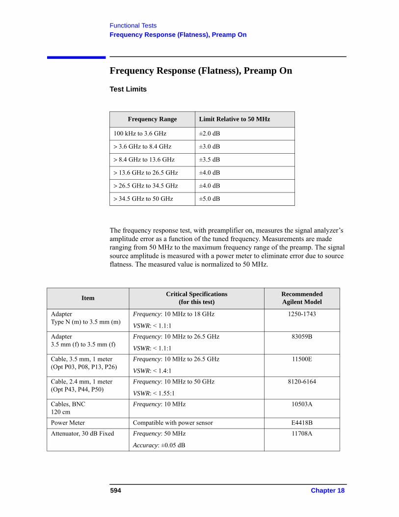
Functional Tests
Frequency Response (Flatness), Preamp On
Frequency Response (Flatness), Preamp On
Test Limits
The frequency response test, with preamplifier on, measures the signal analyzer’s amplitude error as a function of the tuned frequency. Measurements are made ranging from 50 MHz to the maximum frequency range of the preamp. The signal source amplitude is measured with a power meter to eliminate error due to source flatness. The measured value is normalized to 50 MHz.
Frequency Range Limit Relative to 50 MHz
100 kHz to 3.6 GHz ±2.0 dB
> 3.6 GHz to 8.4 GHz ±3.0 dB
> 8.4 GHz to 13.6 GHz ±3.5 dB
> 13.6 GHz to 26.5 GHz ±4.0 dB
> 26.5 GHz to 34.5 GHz ±4.0 dB
> 34.5 GHz to 50 GHz ±5.0 dB
ItemCritical Specifications
(for this test)Recommended Agilent Model
AdapterType N (m) to 3.5 mm (m)
Frequency: 10 MHz to 18 GHz
VSWR: < 1.1:1
1250-1743
Adapter3.5 mm (f) to 3.5 mm (f)
Frequency: 10 MHz to 26.5 GHz
VSWR: < 1.1:1
83059B
Cable, 3.5 mm, 1 meter(Opt P03, P08, P13, P26)
Frequency: 10 MHz to 26.5 GHz
VSWR: < 1.4:1
11500E
Cable, 2.4 mm, 1 meter(Opt P43, P44, P50)
Frequency: 10 MHz to 50 GHz
VSWR: < 1.55:1
8120-6164
Cables, BNC 120 cm
Frequency: 10 MHz 10503A
Power Meter Compatible with power sensor E4418B
Attenuator, 30 dB Fixed Frequency: 50 MHz
Accuracy: ±0.05 dB
11708A
594 Chapter 18
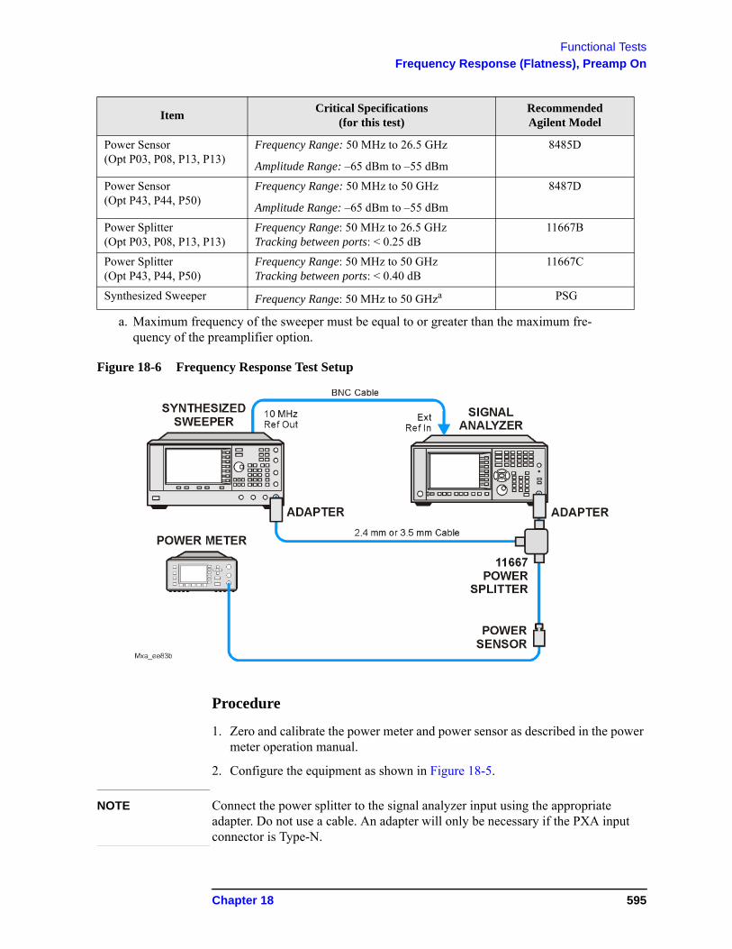
Functional Tests
Frequency Response (Flatness), Preamp On
Figure 18-6 Frequency Response Test Setup
Procedure
1. Zero and calibrate the power meter and power sensor as described in the power meter operation manual.
2. Configure the equipment as shown in Figure 18-5.
NOTE Connect the power splitter to the signal analyzer input using the appropriate adapter. Do not use a cable. An adapter will only be necessary if the PXA input connector is Type-N.
Power Sensor(Opt P03, P08, P13, P13)
Frequency Range: 50 MHz to 26.5 GHz
Amplitude Range: –65 dBm to –55 dBm
8485D
Power Sensor(Opt P43, P44, P50)
Frequency Range: 50 MHz to 50 GHz
Amplitude Range: –65 dBm to –55 dBm
8487D
Power Splitter(Opt P03, P08, P13, P13)
Frequency Range: 50 MHz to 26.5 GHz Tracking between ports: < 0.25 dB
11667B
Power Splitter(Opt P43, P44, P50)
Frequency Range: 50 MHz to 50 GHz Tracking between ports: < 0.40 dB
11667C
Synthesized Sweeper Frequency Range: 50 MHz to 50 GHza PSG
a. Maximum frequency of the sweeper must be equal to or greater than the maximum fre-quency of the preamplifier option.
ItemCritical Specifications
(for this test)Recommended Agilent Model
Chapter 18 595
Functional Tests
Frequency Response (Flatness), Preamp On
3. Assure the signal analyzer’s built-in auto alignment has been performed within the last 24 hours.
4. Press Mode, Spectrum Analyzer, Mode Preset on the signal analyzer, and press Preset on the synthesized sweeper.
5. Set up the synthesized sweeper by pressing:
CW, 50, MHzPower level, –54, dBm
6. Set up the signal analyzer by pressing:
Input/Output, More, Freq Ref In, ExternalFREQ Channel, Center Freq, 50, MHzSPAN X Scale, Span, 50, kHzAMPTD Y Scale, More, Internal Preamp Full RangeAMPTD Y Scale, Attenuation, Mech Atten, 0, dBAMPTD Y Scale, Ref Level, –55, dBm
7. Adjust the synthesized sweeper output power for a power meter reading of –60 dBm ±0.1 dB.
8. On the signal analyzer, press Single.
9. Press the Peak Search key on the signal analyzer to position the marker on the peak of the signal.
10.Refer to Table 18-6, “Frequency Response (Flatness) Results.” Enter the amplitude of the signal displayed on the signal analyzer into the MeasAmp column of Table 18-6.
11. Enter the power meter reading into the PowerMeter column of Table 18-6.
12.Tune the synthesized sweeper and signal analyzer to the next frequency listed in Table 18-6.
13.Enter the power sensor calibration factor into the power meter.
14.For frequencies 3.6 GHz and above, press AMPTD Y Scale, then Presel Center to center the preselector filter for an optimum amplitude measurement.
15.Repeat step 7 through step 14 and complete the remainder of Table 18-6 for the frequency range of your preamp.
16.Compute the measurement error (MeasError = MeasAmp − PowerMeter).
17.Compute the flatness error normalized to 50 MHz:(MeasError − MeasError @ 50 MHz)
18.Enter the computed flatness error value into the FlatNorm column of Table 18-6.
19.Compare the value of FlatNorm to the test limit.
596 Chapter 18
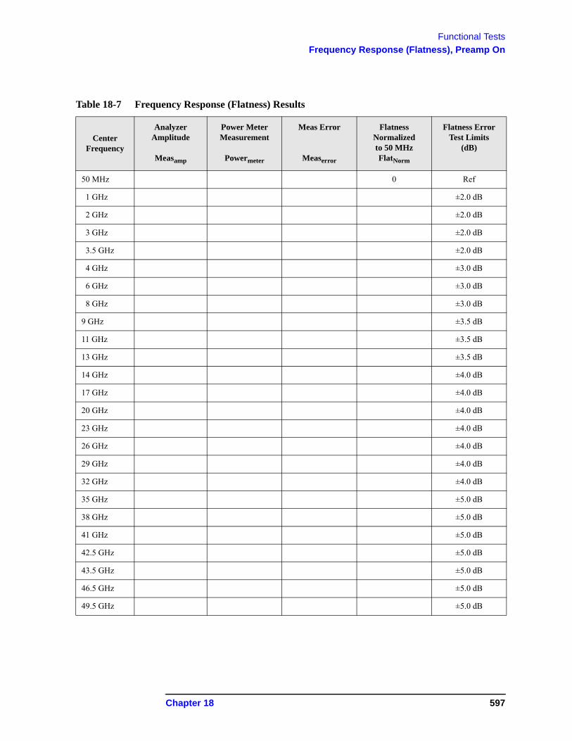
Functional Tests
Frequency Response (Flatness), Preamp On
Table 18-7 Frequency Response (Flatness) Results
CenterFrequency
Analyzer Amplitude
Measamp
Power Meter Measurement
Powermeter
Meas Error
Measerror
Flatness Normalizedto 50 MHzFlatNorm
Flatness ErrorTest Limits
(dB)
50 MHz 0 Ref
1 GHz ±2.0 dB
2 GHz ±2.0 dB
3 GHz ±2.0 dB
3.5 GHz ±2.0 dB
4 GHz ±3.0 dB
6 GHz ±3.0 dB
8 GHz ±3.0 dB
9 GHz ±3.5 dB
11 GHz ±3.5 dB
13 GHz ±3.5 dB
14 GHz ±4.0 dB
17 GHz ±4.0 dB
20 GHz ±4.0 dB
23 GHz ±4.0 dB
26 GHz ±4.0 dB
29 GHz ±4.0 dB
32 GHz ±4.0 dB
35 GHz ±5.0 dB
38 GHz ±5.0 dB
41 GHz ±5.0 dB
42.5 GHz ±5.0 dB
43.5 GHz ±5.0 dB
46.5 GHz ±5.0 dB
49.5 GHz ±5.0 dB
Chapter 18 597
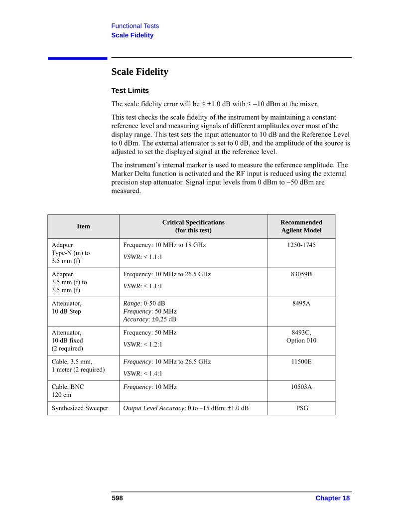
Functional Tests
Scale Fidelity
Scale Fidelity
Test Limits
The scale fidelity error will be ≤ ±1.0 dB with ≤ −10 dBm at the mixer.
This test checks the scale fidelity of the instrument by maintaining a constant reference level and measuring signals of different amplitudes over most of the display range. This test sets the input attenuator to 10 dB and the Reference Level to 0 dBm. The external attenuator is set to 0 dB, and the amplitude of the source is adjusted to set the displayed signal at the reference level.
The instrument’s internal marker is used to measure the reference amplitude. The Marker Delta function is activated and the RF input is reduced using the external precision step attenuator. Signal input levels from 0 dBm to −50 dBm are measured.
ItemCritical Specifications
(for this test)Recommended Agilent Model
AdapterType-N (m) to 3.5 mm (f)
Frequency: 10 MHz to 18 GHz
VSWR: < 1.1:1
1250-1745
Adapter3.5 mm (f) to 3.5 mm (f)
Frequency: 10 MHz to 26.5 GHz
VSWR: < 1.1:1
83059B
Attenuator, 10 dB Step
Range: 0-50 dBFrequency: 50 MHzAccuracy: ±0.25 dB
8495A
Attenuator, 10 dB fixed (2 required)
Frequency: 50 MHz
VSWR: < 1.2:1
8493C, Option 010
Cable, 3.5 mm, 1 meter (2 required)
Frequency: 10 MHz to 26.5 GHz
VSWR: < 1.4:1
11500E
Cable, BNC 120 cm
Frequency: 10 MHz 10503A
Synthesized Sweeper Output Level Accuracy: 0 to –15 dBm: ±1.0 dB PSG
598 Chapter 18
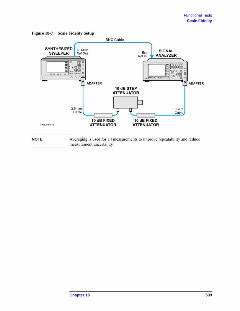
Functional Tests
Scale Fidelity
Figure 18-7 Scale Fidelity Setup
NOTE Averaging is used for all measurements to improve repeatability and reduce measurement uncertainty.
Chapter 18 599
Functional Tests
Scale Fidelity
Procedure
1. Configure the equipment as shown in Figure 18-7.
2. Preset the Source and press Mode, Spectrum Analyzer, Mode Preset on the analyzer.
3. Set up the synthesized sweeper by pressing:
Frequency, 50, MHzAmplitude, +5, dBmRF On/Off, On
4. Set up the signal analyzer by pressing:
Input/Output, More, Freq Ref In, ExternalFREQ Channel, Center Freq, 50, MHzSPAN X Scale, Span, 1, MHz
AMPTD Y Scale, Ref Level, 0, dBmMeas Setup, Average/Hold Number, 10, EnterTrace/Detector, Trace AveragePeak Search
5. Set the external 10 dB step attenuator to 0 dB.
6. Adjust the amplitude on the signal source until the marker amplitude on the analyzer reads –15 dBm ± 0.2 dB.
7. On the analyzer, press the Single, Restart to trigger a 10 sweep average.
8. On the analyzer, activate the Marker Delta function by pressing Peak Search, Marker Delta.
9. Perform the following steps for each attenuator setting listed in the table below:
a. Select the next External attenuator setting.
b. Press the Restart key to trigger a 10 sweep average.
c. Enter the delta marker value into Table 18-8.
d. Check delta marker reading against the test limits.
600 Chapter 18
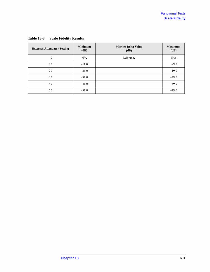
Functional Tests
Scale Fidelity
Table 18-8 Scale Fidelity Results
External Attenuator SettingMinimum
(dB)Marker Delta Value
(dB)Maximum
(dB)
0 N/A Reference N/A
10 –11.0 –9.0
20 –21.0 –19.0
30 –31.0 –29.0
40 –41.0 –39.0
50 –51.0 –49.0
Chapter 18 601
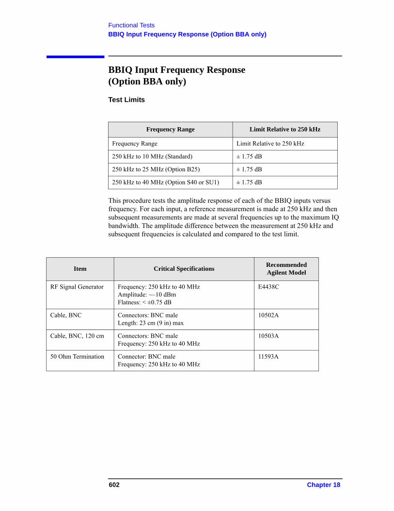
Functional Tests
BBIQ Input Frequency Response (Option BBA only)
BBIQ Input Frequency Response (Option BBA only)
Test Limits
This procedure tests the amplitude response of each of the BBIQ inputs versus frequency. For each input, a reference measurement is made at 250 kHz and then subsequent measurements are made at several frequencies up to the maximum IQ bandwidth. The amplitude difference between the measurement at 250 kHz and subsequent frequencies is calculated and compared to the test limit.
Frequency Range Limit Relative to 250 kHz
Frequency Range Limit Relative to 250 kHz
250 kHz to 10 MHz (Standard) ± 1.75 dB
250 kHz to 25 MHz (Option B25) ± 1.75 dB
250 kHz to 40 MHz (Option S40 or SU1) ± 1.75 dB
Item Critical SpecificationsRecommended Agilent Model
RF Signal Generator Frequency: 250 kHz to 40 MHzAmplitude: ~–10 dBmFlatness: < ±0.75 dB
E4438C
Cable, BNC Connectors: BNC maleLength: 23 cm (9 in) max
10502A
Cable, BNC, 120 cm Connectors: BNC maleFrequency: 250 kHz to 40 MHz
10503A
50 Ohm Termination Connector: BNC maleFrequency: 250 kHz to 40 MHz
11593A
602 Chapter 18
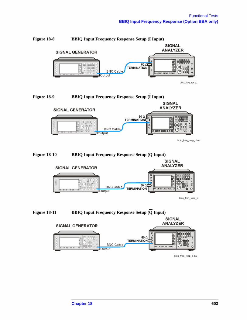
Functional Tests
BBIQ Input Frequency Response (Option BBA only)
Figure 18-8 BBIQ Input Frequency Response Setup (I Input)
Figure 18-9 BBIQ Input Frequency Response Setup (I Input)
Figure 18-10 BBIQ Input Frequency Response Setup (Q Input)
Figure 18-11 BBIQ Input Frequency Response Setup (Q Input)
Chapter 18 603
Functional Tests
BBIQ Input Frequency Response (Option BBA only)
Procedure
1. On the X-Series analyzer, press Mode, IQ Analyzer (Basic). Press Mode Preset.
2. Press Input/Output, I/Q (to change to I/Q inputs), I/Q (to bring up the I/Q input menu), I/Q Cable Calibrate. Follow the instructions on screen. Use the short BNC cable listed above to perform the calibration. This process has several steps and will take about 3 minutes to perform.
3. Press I/Q Path, I+jQ, I Setup, Differential (On). Press Return, Q Setup, Q Same as I (Yes).
4. Preset the RF Signal Generator and set the controls as follows:
Frequency 250 kHzAmplitude –10 dBmRF On
NOTE Once the RF Signal Generator’s Amplitude is set, do not change the RF Signal Generator’s Amplitude setting during the rest of this procedure.
5. Connect the longer BNC cable between the RF Signal Generator’s RF OUTPUT and the I input of the X-Series analyzer, see Figure 18-8
6. Connect the 50 Ohm termination to the I input of the X-Series analyzer, see Figure 18-8
7. Press Mode Preset on the X-Series analyzer. Press System, Show, System. Note if either of the options listed below are present:
N9030A-B25N9030A-S40N9030A-B40
8. If none of the options listed in step 7 are present, the maximum IQ bandwidth is 10 MHz
9. If N9030A-B25 is present, but N9030A-S40 and N9030A-B40 are not present, the maximum IQ bandwidth is 25 MHz
10. If either N9030A-S40 or N9030A-B40 is present, the maximum IQ bandwidth is 40 MHz.
11. Press FREQ on the X-Series analyzer and set the Center Freq equal to one half the maximum IQ bandwidth determined above. For example, if the maximum IQ bandwidth is 40 MHz, set the Center Freq to 20 MHz.
12.Press SPAN on the X-Series analyzer and set the Span equal to the maximum IQ bandwidth determined above.
13.Press BW on the X-Series analyzer and set the Res BW to 100 kHz.
604 Chapter 18
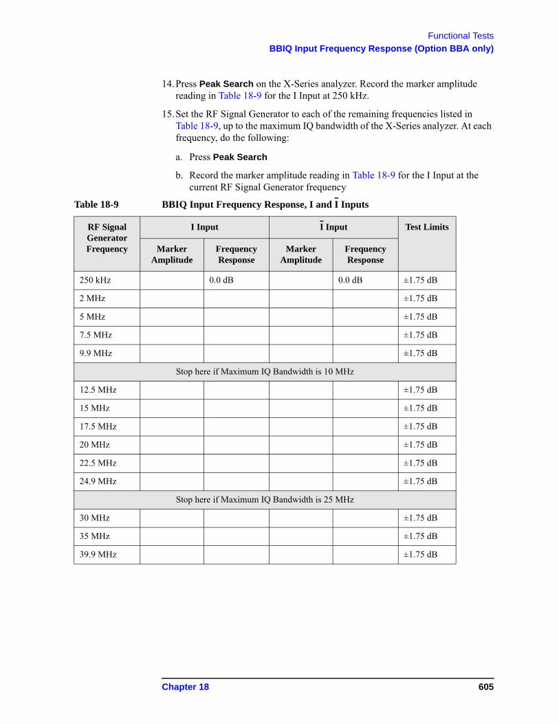
Functional Tests
BBIQ Input Frequency Response (Option BBA only)
14.Press Peak Search on the X-Series analyzer. Record the marker amplitude reading in Table 18-9 for the I Input at 250 kHz.
15.Set the RF Signal Generator to each of the remaining frequencies listed in Table 18-9, up to the maximum IQ bandwidth of the X-Series analyzer. At each frequency, do the following:
a. Press Peak Search
b. Record the marker amplitude reading in Table 18-9 for the I Input at the current RF Signal Generator frequency
Table 18-9 BBIQ Input Frequency Response, I and I Inputs
RF Signal Generator Frequency
I Input I Input Test Limits
Marker Amplitude
Frequency Response
Marker Amplitude
Frequency Response
250 kHz 0.0 dB 0.0 dB ±1.75 dB
2 MHz ±1.75 dB
5 MHz ±1.75 dB
7.5 MHz ±1.75 dB
9.9 MHz ±1.75 dB
Stop here if Maximum IQ Bandwidth is 10 MHz
12.5 MHz ±1.75 dB
15 MHz ±1.75 dB
17.5 MHz ±1.75 dB
20 MHz ±1.75 dB
22.5 MHz ±1.75 dB
24.9 MHz ±1.75 dB
Stop here if Maximum IQ Bandwidth is 25 MHz
30 MHz ±1.75 dB
35 MHz ±1.75 dB
39.9 MHz ±1.75 dB
Chapter 18 605
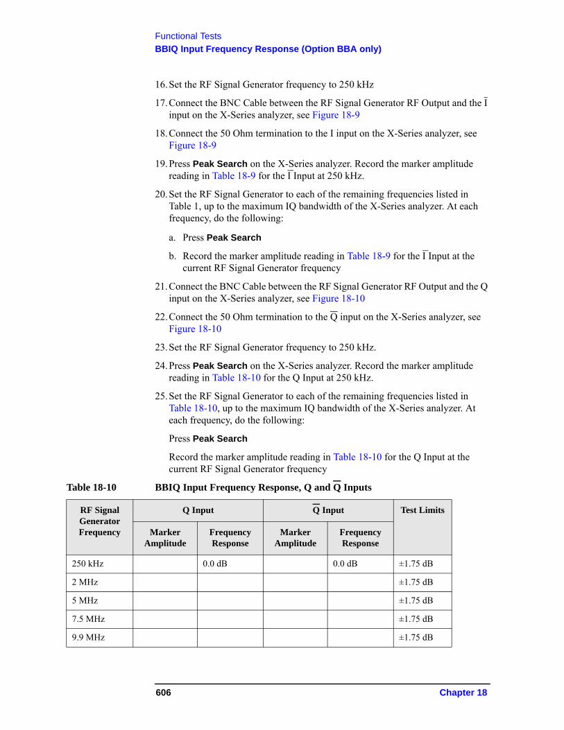
Functional Tests
BBIQ Input Frequency Response (Option BBA only)
16.Set the RF Signal Generator frequency to 250 kHz
17.Connect the BNC Cable between the RF Signal Generator RF Output and the I input on the X-Series analyzer, see Figure 18-9
18.Connect the 50 Ohm termination to the I input on the X-Series analyzer, see Figure 18-9
19.Press Peak Search on the X-Series analyzer. Record the marker amplitude reading in Table 18-9 for the I Input at 250 kHz.
20.Set the RF Signal Generator to each of the remaining frequencies listed in Table 1, up to the maximum IQ bandwidth of the X-Series analyzer. At each frequency, do the following:
a. Press Peak Search
b. Record the marker amplitude reading in Table 18-9 for the I Input at the current RF Signal Generator frequency
21.Connect the BNC Cable between the RF Signal Generator RF Output and the Q input on the X-Series analyzer, see Figure 18-10
22.Connect the 50 Ohm termination to the Q input on the X-Series analyzer, see Figure 18-10
23.Set the RF Signal Generator frequency to 250 kHz.
24.Press Peak Search on the X-Series analyzer. Record the marker amplitude reading in Table 18-10 for the Q Input at 250 kHz.
25.Set the RF Signal Generator to each of the remaining frequencies listed in Table 18-10, up to the maximum IQ bandwidth of the X-Series analyzer. At each frequency, do the following:
Press Peak Search
Record the marker amplitude reading in Table 18-10 for the Q Input at the current RF Signal Generator frequency
Table 18-10 BBIQ Input Frequency Response, Q and Q Inputs
RF Signal Generator Frequency
Q Input Q Input Test Limits
Marker Amplitude
Frequency Response
Marker Amplitude
Frequency Response
250 kHz 0.0 dB 0.0 dB ±1.75 dB
2 MHz ±1.75 dB
5 MHz ±1.75 dB
7.5 MHz ±1.75 dB
9.9 MHz ±1.75 dB
606 Chapter 18
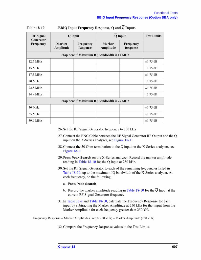
Functional Tests
BBIQ Input Frequency Response (Option BBA only)
26.Set the RF Signal Generator frequency to 250 kHz
27.Connect the BNC Cable between the RF Signal Generator RF Output and the Q input on the X-Series analyzer, see Figure 18-11
28.Connect the 50 Ohm termination to the Q input on the X-Series analyzer, see Figure 18-11
29.Press Peak Search on the X-Series analyzer. Record the marker amplitude reading in Table 18-10 for the Q Input at 250 kHz.
30.Set the RF Signal Generator to each of the remaining frequencies listed in Table 18-10, up to the maximum IQ bandwidth of the X-Series analyzer. At each frequency, do the following:
a. Press Peak Search
b. Record the marker amplitude reading in Table 18-10 for the Q Input at the current RF Signal Generator frequency
31. In Table 18-9 and Table 18-10, calculate the Frequency Response for each input by subtracting the Marker Amplitude at 250 kHz for that input from the Marker Amplitude for each frequency greater than 250 kHz.
32.Compare the Frequency Response values to the Test Limits.
Stop here if Maximum IQ Bandwidth is 10 MHz
12.5 MHz ±1.75 dB
15 MHz ±1.75 dB
17.5 MHz ±1.75 dB
20 MHz ±1.75 dB
22.5 MHz ±1.75 dB
24.9 MHz ±1.75 dB
Stop here if Maximum IQ Bandwidth is 25 MHz
30 MHz ±1.75 dB
35 MHz ±1.75 dB
39.9 MHz ±1.75 dB
Table 18-10 BBIQ Input Frequency Response, Q and Q Inputs
RF Signal Generator Frequency
Q Input Q Input Test Limits
Marker Amplitude
Frequency Response
Marker Amplitude
Frequency Response
Frequency Response = Marker Amplitude (Freq > 250 kHz) – Marker Amplitude (250 kHz)
Chapter 18 607
Functional Tests
BBIQ Input Frequency Response (Option BBA only)
608 Chapter 18
19 Instrument Software
609
Instrument Software
What You Will Find in This Chapter
What You Will Find in This Chapter
Instrument Software Overview on page 611
Software Licensing on page 611
Software Updates on page 612
Instrument Measurement Application Software on page 612
89601 VSA Software on page 612
610 Chapter 19
Instrument Software
Instrument Software Overview
Instrument Software Overview
The instrument software, installed in every instrument, contains not only the spectrum analyzer measurement application, but also all of the other currently available measurement applications. However, only the licensed applications will be seen and available for use.
To view the currently licensed measurement applications press System, Show, System. In addition to listing the application model number and description you will also see the revision of each. However, the complete package itself also has a revision associated with it, which can also be found on this screen as the “Instrument S/W Revision”.
Since the instrument application software is distributed in one complete package, when an update is installed they are all updated at the same time. One of the benefits of this is that you cannot have revisions that are incompatible with each other installed in an instrument. However, there is one exception to this, which would be the 89601A VSA software. While the latest revision of the 89601A VSA software is installed in each instrument as it left the factory, it must be updated, and kept in sync with the rest of the instrument application software independently.
Software Licensing
All application software needs to have a valid license in order to be available for use. This also includes the spectrum analyzer application (N9060A).
Chapter 19 611
Instrument Software
Software Updates
Software Updates
Instrument Measurement Application Software
Updates are installed much like most other types of commercial software packages. The latest revision of the software, along with complete installation instructions, can be obtained by one of two methods, which are:
Web Download:
The latest revision of the software can be downloaded from:
www.agilent.com/find/xseries_software
Software On Media:
The latest revision of the software can be purchased on a USB storage device as option N9030AK-SWM.
89601 VSA Software
Updates for the 89601 VSA software can be downloaded from:
http://www.agilent.com/find/89600_sw_download
The revision of the 89601 VSA software must be compatible with the revision of the instrument measurement application software package that is installed in the instrument. To determine what revisions are compatible, and if a further updates are required, please see the software compatibility information on the instrument measurement application software download web page listed above.
612 Chapter 19
Index
RF front endsee A13 RF front end assembly
Numerics
50 ohm load, 2150 ohm/75 ohm minimum loss pad, 2175 ohm matching transformer, 21
A
A10 input attenuatordescription, 151, 177part number, 382removal, 438, 473
A10 Input Attenuator B troubleshooting, 159, 185
A11 low band switchdescription, 152, 178part number, 382removal, 441, 475
A11 Low Band Switch troubleshooting, 158, 184
A12 YTFdescription, 152, 178part number, 382removal, 444, 447, 478, 481
A13 front end assembly troubleshooting, 160, 186
A13 Front End Assembly Verification, 170, 196
A13 Front End Input Verification, 167, 193
A13 RF front end assemblydescription, 153, 179removal, 491
A14 L.O. synthesizer assemblydescription, 152, 178, 253part number, 382removal, 496troubleshooting, 257
A15 front end control assemblydescription, 154, 180, 201part number, 382removal, 494troubleshooting, 205
A16 reference assemblydescription, 269part number, 382removal, 498troubleshooting, 271
A1A2 front panel interface boarddescription, 320part number, 382removal, 541, 549
A1A3 LCDdescription, 320part number, 382removal, 539, 547
troubleshooting, 65A1A4 Inverter Board
removal, 538A1A4 inverter board
part number, 382removal, 549
A1A4 LCD Inverter Boarddescription, 320
A1A5 front panel daughter boardpart number, 382removal, 541, 549
A1A5 Front Panel USB Interface Board
description, 320A2 analog IF assembly
description, 229part number, 382removal, 516troubleshooting, 233
A25 wideband analog IF assemblyremoval, 501
A26 wideband digital IF assemblyremoval, 501
A3 digital IF assemblydescription, 240part number, 382removal, 516troubleshooting, 243
A4 CPU assemblydescription, 281part number, 382removal, 509troubleshooting, 281
A4BT1 CPU board batterydescription, 3disposal, 3part number, 382post-repair setup, 554replacement, 509
A5 disk drivedescription, 294troubleshooting, 294
A5 hard disk drivepart number, 382recovery process, 298removal, 510
A6 power supplydescription, 303part number, 382removal, 507troubleshooting, 307
A7 midplanedescription, 310part number, 382troubleshooting, 312
A7 midplane assemblypart number, 382
A8 motherboarddescription, 317part number, 382removal, 520troubleshooting, 319
A9 input attenuatordescription, 151, 177part number, 382removal, 438, 473
A9 Input Attenuator A and A10 Input Attenuator B Verification, 168, 194
A9 Input Attenuator A troubleshooting, 159, 185
AC probe, 21access to service menus, 360accessories, 20
50 ohm load, 2150 ohm/75 ohm minimum loss pad,
2175 ohm matching transformer, 21AC probe, 21broadband preamplifiers, 22power splitters, 22RF limiters, 22transient limiters, 22
adjustmentsequipment, 30required test equipment, 30test equipment, 30
advisory messages, 81after repairs
see post-repair procedures, 553Agilent Technologies
contacting, 41Sales and Service offices, 41splash screen, 51
Align menu description, 374alignment failure, 70Alignments key, 49amplifiers, 22amplitude accuracy test, 586
option 1DS, 589amplitude linearity test, 598analog IF
see A2 analog IF assemblyapplication updating, 611attenuators, removal, 438, 473
B
B1, B2 fanspart number, 382troubleshooting, 60
B1, B2, B3 fansremoval, 525
backlights, 66bail handle
Index-613
Index
part number, 382Band Lock menu description, 371basics, troubleshooting, 49battery
see A4BT1 CPU board batteryBBIQ frequency response, 602before troubleshooting, 23blank display, 65block diagrams, 335boot process
problems, 54boot up process, 50broadband preamplifiers, 22
C
cablespart numbers, 382
calibration application software, 27call centers, 41cautions and warnings, 23chassis parts
part numbers, 382checking firmware revision, 49computer block diagram, 335connector
see RF input connectorcontacting Agilent, 41corrections menu description, 369CPU assembly
see A4 CPU assembly
D
DANL test, 579daughter board
see A1A5 front panel daughter boardDC probes
use of, 21diagnostics menus, 359digital IF
see A3 digital IF assemblydisk drive
see A5 hard disk drivedisk drive recovery process, 298display
see A1A3 LCDdisplay output, rear panel, 65displayed average noise level. See
DANL, 579dress case
see outer case
E
electronic attenuator path, 150, 176Electronic Attenuator Test (Option
EA3) troubleshooting, 161, 187electrostatic discharge, 25
enabling spread spectrum, 565entitlement certificate, 17equipment
adjustments, 30functional tests, 576performance verification tests, 30warm-up time, 575
error messages, 49, 79, 80example, 82format, 81viewing messages in queue, 83
error queuescapacity, 82clearing, 83front panel, 82overflow handling, 83remote interface (SCPI), 82viewing entries, 83
ESD Information, 25ESD safety accessories, 22external hardware, 397, 398, 401,
402, 404, 406, 407, 408, 413, 414, 416, 417, 418, 419, 420, 421, 422, 424, 542, 543, 544
external VGA monitor, 65
F
fanssee B1, B2 fans
firmware, 49firmware revision, checking, 49firmware updating, 611First LO Level Verification, 169, 195frequency ranges, 149, 175frequency readout accuracy test, 581frequency response
(flatness) test, 590BBIQ, 602
frequency response (flatness) testpreamp on, 594
front end assemblysee A13 RF front end assembly
front end control boardsee A15 front end control assembly
front end troubleshooting kit, 28front frame
description, 320part number, 382removal, 531
front panel error queue, 82front panel interface
see A1A2 front panel interface board, 382
functional testingperformance verification, 574
functional tests, 49before performing, 575
equipment list, 576introduction, 573vs performance verification tests,
574warm-up time, 575See also individual functional tests,
573Functional Tests Guide on CD-ROM,
20
G
Getting Started Guide on CD-ROM, 20green LED, 51
H
handlesee bail handle
hard disk drivesee A5 hard disk drive
hardwareexternal, 397, 398, 401, 402, 404,
406, 407, 408, 413, 414, 416, 417, 418, 419, 420, 421, 422, 424, 542, 543, 544
high band mixing equations, 171, 197high band path, 149, 175High Band Preamp (Option P08, P13,
P26) troubleshooting, 170, 196high band signal level verification, 77high band troubleshooting, 163, 167,
189, 193
I
IF Flatness menu description, 369initial alignment failure, 70initialization problem, 69input attenuators
see A9 and A10 input attenuatorinput connector
see RF input connectorinstrument
return for service, 44instrument frequency ranges, 149, 175instrument messages, 79Instrument Messages Guide on
CD-ROM, 20instrument options, 18instrument packaging, 44instrument serial number, 43instrument upgrade, 18internal alignments, 70inverter board
see A1A4 inverter board
K
keyboard
Index-614
Index
USB, 29keypad
part number, 382removal, 541, 549
L
LCDsee A1A3 LCD
LEDfront panel, 49green, 51power on, 56standby, 54yellow, 51, 54
license key, 17licensing software, 611limiters
RF and transient, 22LO Band Lock menu description, 372load, 50 ohm, 21loading MXA software, 297low band mixing equations, 162, 188low band path, 149, 175low band preamplifier path, 150, 176low band signal level verification, 76low band switch
see A11 low band switchlow band troubleshooting, 155, 181Low Noise Path (Option LNP)
troubleshooting, 171, 197
M
major assembly locations, 431manual set, 20measurement application updating,
611Measurement Guides and
Programming Examples Guides on CD-ROM, 20
messagesadvisories, 81error, 79errors, 80warnings, 81
messages, warning, 81Microwave Preselector Bypass (Option
MPB) troubleshooting, 171, 197midplane
see A7 midplanemidplane assembly
removal, 504midplane bracket
part number, 382motherboard
see A8 motherboardmouse
USB, 29
N
N7814Asee calibration application software
O
operating system, 17problems, 65
options, 20, 322original instrument packing, 44other instrument packing, 45outer case, removal, 432overview, MXA signal analyzer, 17
P
packaging, 44parts
replaceable, 382performance verification tests
equipment, 30required test equipment, 30test equipment, 30
performance verification tests vs functional tests, 574
post-repair procedures, 553power amplifiers, 22power on LED, 56power splitters, 22power supply
see A6 power supply, 382preamplifiers, 22preload measurement applications, 50preselector
see A12 YTFprobes
AC and DC, 21
R
rear panelremoval, 506
rear panel display output, 65recovery process, 298reference assembly
see A16 reference assemblyreference bracket
part number, 382removal, 434
removesee individual assemblies
repairssee post-repair procedures
replacesee individual assemblies
replaceable parts, 382required equipment, 30required test equipment
adjustments, 30
performance verification tests, 30troubleshooting, 30
return instrument for service, 44RF area components, Option 503, 508,
513, 526, 436RF area components, Option 543, 544,
550, 471RF Flatness menu description, 369RF input connector
part number, 382removal, 529
RF limiters, 22RF path block diagram, 335RF section
description, 149, 175RPG knob
part number, 382
S
Safety Information, 3, 429Sales and Service offices, 41SCPI interface error queue, 82second harmonic distortion test, 583separate analog IF assembly and digital
IF assembly, 518serial number, 43service
equipment, 27returning your instrument, 44tools, 27, 430
service menus, 359service strategy, 17signal level verification, 76Snapshot Alignments menu
description, 369software licensing, 611specifications, 49Specifications Guide on CD-ROM, 20splash screen, 51, 62, 64splitters, 22spread spectrum, 565standby LED, 54static safety accessories, 22static-safe workstation, 25status messages, 81storage device
USB, 29support URL, 41support web site, 41synthesizer
see A14 L.O. synthesizer assembly
T
test equipmentadjustments, 30performance verification tests, 30post-repair, 552
Index-615
Index
troubleshooting, 30tests. See functional teststimebase key description, 368top brace
part number, 382removal, 434
transient limiter, 22troubleshooting
basics, 49before you start, 23equipment needed, 30high band, 163, 189low band, 155, 181see individual assemblies
U
updating firmware, 611
updating measurement applications, 611
upgrades, 18URL, 41, 49USB keyboard and mouse, 29USB storage device, 29User’s/Programmers Reference Guides
on CD-ROM, 20
V
video controller, 69video signal path integrity, 69
W
warning messages, 81warnings and cautions, 23
web site URL, 49wideband analog IF assembly
see A25 wideband analog IF assembly
wideband digital IF assemblysee A26 wideband digital IF
assembly
Y
yellow LED, 51, 54yig filter
see A12 YTFYTF
see A12 YTF
Index-616


