Embed Size (px)
Citation preview
6080A/ANSYNTHESIZED SIGNAL GENERATOR
Service Manual
P/N 868906October 1989©1989, John Fluke Mfg. Co. Inc. All rights reserved PO Box C9090 Everett WA 98206
WARRANTY
The JOHN FLUKE MFG. CO., INC warrants each instrument it manufactures to be free from defects inmaterial and workmanship under normal use for 2 years from the date of purchase. This warranty extendsonly to the original purchaser. This warranty shall not apply to fuses, disposable batteries, or any product orparts that have been subject to misuse, neglect, accident, or abnormal conditions of operation.
In the event of failure of a product covered by this warranty, JOHN FLUKE MFG. CO., INC will repair andcalibrate an instrument returned to an authorized Service Center within 2 years of the original purchase;provided the warrantor's examination discloses to its satisfaction that the product was defective. Thewarrantor may, at its option, replace the product in lieu of repair. With regard to any instrument returnedwithin 2 years of the original purchase, said repairs or replacement will be made without charge. If the failurehas been caused by misuse, neglect, accident, or abnormal conditions of operation, repairs will be billed at anominal cost. In such case, an estimate will be submitted before work is stated if requested.
If any failure occurs, the following steps should be taken:
1. Notify the JOHN FLUKE MFG. CO., INC or nearest Service Center, giving full details of thedifficulty. Include the model number, type number, and serial number.
On receipt of this information, service data or shipping instructions will be forwarded to you.
2. On receipt of the shipping instructions, forward the instrument, transportation prepaid.
Repairs will be made at the Service Center and the instrument will be returned prepaid.
SHIPPING TO MANUFACTURER FOR REPAIR OR ADJUSTMENT
All shipment of JOHN FLUKE MFG. CO., INC instruments should be shipped in the original packing carton (ifavailable). If the original carton is not available, use any suitable container that is rigid and of adequate size. Ifa substitute container is used, the instrument should be wrapped in paper and surrounded with at least fourinches of shock-absorbing material.
Table of Contents
SECTION TITLE PAGE
1 INTRODUCTION AND SPECIFICATIONS 1-1
1-1. INTRODUCTION 1-11-2. UNPACKING THE SIGNAL GENERATOR 1-11-3. SAFETY 1-21-4. ACCESSORIES 1-31-5. SIGNAL GENERATOR SPECIFICATIONS 1-3
2 THEORY OF OPERATION 2-1
2-1. INTRODUCTION 2-12-2. GENERAL DESCRIPTION 2-12-3. Front Panel Section 2-22-4. Upper/Lower Module Sections 2-22-5. Rear Panel Section 2-22-6. FUNCTIONAL DESCRIPTION 2-22-7. Frequency 2-22-8. Frequency Modulation 2-42-9. Phase Modulation 2-42-10. Output/Level Control 2-52-11. Amplitude Modulation 2-52-12. Pulse Modulation 2-52-13. Internal Modulation Oscillator 2-62-14. Power Supply Description 2-62-15. DIGITAL CONTROLLER SOFTWARE DESCRIPTION 2-62-16. User Interface 2-62-17. Calibration/Compensation Memory 2-72-18. Self-Test 2-72-19. Status Signals 2-7
3 CLOSED-CASE CALIBRATION 3-1
3-1. INTRODUCTION 3-13-2. Front Panel Calibration 3-23-3. Remote Calibration 3-23-4. Calibration Data 3-33-5. AM CALIBRATION 3-43-6. Front Panel AM Calibration Procedure 3-43-7. Remote AM Calibration Procedure 3-6
i (continued on page ii)
TABLE OF CONTENTS, continued
SECTION TITLE PAGE
3-8. FM CALIBRATION 3-73-9. Front Panel FM Calibration Procedure 3-83-10. Remote FM Calibration 3-93-11. RF LEVEL CALIBRATION 3-103-12. Front Panel Level Calibration Procedure 3-113-13. Remote Level Calibration Procedure 3-133-14. REFERENCE OSCILLATOR CALIBRATION 3-143-15. Front Panel Reference Oscillator Calibration Procedure 3-153-16. Remote Reference Oscillator Calibration Procedure 3-16
4 PERFORMANCE TESTS 4-1
4-1. INTRODUCTION 4-14-2. TEST EQUIPMENT 4-14-3. POWER-ON TEST 4-44-4. FREQUENCY ACCURACY TEST 4-54-5. SYNTHESIS TEST 4-54-6. HIGH-LEVEL ACCURACY TEST 4-64-7. MID-LEVEL ACCURACY TEST 4-84-8. LOW-LEVEL ACCURACY TEST 4-94-9. ALTERNATE-LEVEL ACCURACY TEST 4-104-10. FLATNESS TEST 4-134-11. OUTPUT LEAKAGE TEST 4-144-12. HARMONIC AND LINE-RELATED SPURIOUS TEST 4-154-13. PHASE NOISE AND NON-HARMONIC SPURIOUS TESTS 4-164-14. MODULATION TESTS 4-174-15. VOLTAGE STANDING-WAVE RATIO (VSWR) TESTS 4-234-16. PULSE TESTS 4-24
5 ACCESS PROCEDURES 5-1
5-1. INTRODUCTION AND SAFETY 5-15-2. LOCATION OF MAJOR ASSEMBLIES 5-35-3. ACCESS INSTRUCTIONS 5-35-4. Removing the Front Panel Section 5-35-5. Removing the Rear Panel Section 5-35-6. Removing the A2 Coarse Loop PCA 5-45-7. Removing the A3 Sub-Synthesizer VCO PCA 5-45-8. Removing the A4 Sub-Synthesizer PCA 5-55-9. Removing the A5 Coarse Loop VCO PCA 5-55-10. Removing the A6 Mod Oscillator PCA 5-55-11. Removing the A8 Output PCA 5-55-12. Removing the A9 Sum Loop VCO PCA 5-65-13. Removing the A10 Premodulator PCA 5-65-14. Removing the A11 Modulation Control PCA 5-65-15. Removing the A12 Sum Loop PCA 5-75-16. Removing the A13 Controller PCA 5-75-17. Removing the A14 FM PCA 5-85-18. Removing the A20 Attenuator/RPP Assembly 5-85-19. Removing the A22 Delay Cable Assembly 5-8
ii (continued on page iii)
TABLE OF CONTENTS, continued
SECTION TITLE PAGE
6 CIRCUIT DESCRIPTIONS, TROUBLESHOOTING, AND ALIGNMENT 6-1
6-1. INTRODUCTION 6-16-2. MODULE REPLACEMENT 6-46-3. A1 Display PCA 6-56-4. A2 Coarse Loop PCA 6-56-5. A3 Sub-Synthesizer PCA 6-56-6. A4 Sub-Synthesizer PCA 6-56-7. A5 Coarse Loop VCO PCA 6-56-8. A6 Mod Oscillator PCA 6-56-9. A7 Relay Driver PCA 6-56-10. A8Output PCA 6-56-11. A9 Sum Loop VCO PCA 6-56-12. A10 Premodulator PCA 6-66-13. A11 Modulation Control PCA 6-66-14. A12 Sum Loop PCA 6-66-15. A13 Controller PCA 6-66-16. A14 FM Board PCA 6-66-17. A15 Power Supply PCA 6-66-18. A19 Switch PCA 6-66-19. A20 Attenuator/RPP Assembly (A7, A21, A30) 6-66-20. A22 Delay Line Assembly (A25+A26+Delay Cable+Trim Cable) ....... 6-66-21. UPDATING COMPENSATION MEMORY WITH
MODULE EXCHANGE DATA 6-76-22. PARTS REPLACEMENT 6-86-23. SELF-TEST DESCRIPTION 6-86-24. Digital Tests 6-86-25. AM Tests 6-96-26. FM Tests 6-96-27. øM Tests 6-96-28. DCFM Test 6-106-29. Coarse Loop Tests 6-116-30. Sub-Synthesizer Tests 6-116-31. Sum Loop Tests 6-116-32. RF Output Tests 6-126-33. Pulse Modulator Tests 6-126-34. Filter Tests 6-126-35. STATUS SIGNALS AND STATUS CODES 6-136-36. SOFTWARE DIAGNOSTIC FUNCTIONS 6-146-37. Digital Control Latch Test 6-146-38. Instrument Diagnostic State 6-146-39. Set Internal DACs 6-146-40. Display Synthesizer Loop Frequencies 6-15
6A POWER SUPPLY 6A-1
6A-1. POWER SUPPLY BLOCK DIAGRAM 6A-16A-2. POWER SUPPLY CIRCUIT DESCRIPTION 6A-16A-3. POWER SUPPLY TROUBLESHOOTING 6A-46A-4. Troubleshooting Procedure 6A-46A-5. POWER SUPPLY ADJUSTMENT PROCEDURE 6A-5
iii (continued on page iv)
TABLE OF CONTENTS, continued
SECTION TITLE PAGE
6B DIGITAL CONTROLLER 6B-1
6B-1. DIGITAL CONTROLLER BLOCK DIAGRAM 6B-16B-2. DIGITAL CONTROLLER CIRCUIT DESCRIPTION (A13) 6B-16B-3. Microprocessor 6B-16B-4. Memory 6B-16B-5. Memory Control 6B-36B-6. Front Panel Interface 6B-36B-7. IEEE-488 Interface 6B-36B-8. Attenuator Control Interface 6B-36B-9. Module I/O 6B-36B-10. Status and Control 6B-46B-11. DIGITAL CONTROLLER TROUBLESHOOTING 6B-46B-12. RF Control 6B-46B-13. Microprocessor Kernel 6B-56B-14. Clock 6B-56B-15. Power-On Reset 6B-56B-16. Unused Microprocessor Inputs 6B-56B-17. Bus Error 6B-56B-18. Interrupts 6B-56B-19. Microprocessor Bus 6B-66B-20. Address Decoder 6B-66B-21. I/O Diagnostic Tests 6B-76B-22. CALIBRATION/COMPENSATION MEMORY 6B-86B-23. Calibration/Compensation Memory Status 6B-86B-24. Repairing Calibration/Compensation Memory Checksum Errors .. 6B-96B-25. Calibration/Compensation Memory Origin Status 6B-96B-26. FRONT PANEL CIRCUIT DESCRIPTION 6B-96B-27. Display PCA 6B-106B-28. Data Communications 6B-106B-29. Display Filament Voltage 6B-106B-30. Bright-Digit Effect 6B-106B-31. Switchboard Interface 6B-106B-32. Remote Footswitch 6B-106B-33. Edit Knob Interface 6B-116B-34. Display Blanking 6B-116B-35. Operate/Standby Selection 6B-116B-36. FRONT PANEL TROUBLESHOOTING 6B-116B-37. Display and Controls 6B-11
6C FREQUENCY SYNTHESIS 6C-1
6C-1. FREQUENCY FAULT TREE 6C-16C-2. SUB-SYNTHESIZER BLOCK DIAGRAM 6C-16C-3. SUB-SYNTHESIZER CIRCUIT DESCRIPTION (A4) 6C-16C-4. SUB-SYNTHESIZER TROUBLESHOOTING 6C-96C-5. SUB-SYNTHESIZER ADJUSTMENTS 6C-136C-6. Steering DAC Full Scale Adjustment 6C-136C-7. Lower Clamp Adjustment, R99 6C-136C-8. Upper Clamp Adjustment, R98 6C-146C-9. SSB Mixer LO Drive Adjustment, R106 6C-146C-10. 10-kHz Notch Adjustment, L56 6C-15
IV (continued on page v)
TABLE OF CONTENTS, continued
SECTION TITLE PAGE
6C-11. SUB-SYNTHESIZER VCO (A3) CIRCUIT DESCRIPTION 6C-166C-12. SUB-SYNTHESIZER VCO TROUBLESHOOTING 6C-166C-13. COARSE LOOP CIRCUIT DESCRIPTION (A2) 6C-176C-14. REFERENCE SECTION BLOCK DIAGRAM 6C-176C-15. COARSE LOOP BLOCK DIAGRAM 6C-206C-16. COARSE LOOP TROUBLESHOOTING 6C-226C-17. COARSE LOOP PCA ADJUSTMENTS 6C-266C-18. Discriminator Video Amplifier Offset Adjustment, R102 6C-266C-19. Steering Gain Adjustment, R221 6C-286C-20. Acquisition Oscillator Level Adjustment, R227 6C-286C-21. 40-MHz Oscillator Adjustment, L601 6C-286C-22. 80-MHz Filter Tuning, L612 and L613 6C-296C-23. 80-MHz Level Adjustment, R617 6C-306C-24. 2-MHz Notch Adjustment, L205 6C-306C-25. Alternate Reference Frequency Selection 6C-316C-26. COARSE LOOP VCO (A5) CIRCUIT DESCRIPTION 6C-316C-27. COARSE LOOP VCO TROUBLESHOOTING 6C-326C-28. SUM LOOP BLOCK DIAGRAM 6C-326C-29. SUM LOOP (A12) CIRCUIT DESCRIPTION 6C-346C-30. RF Section 6C-346C-31. Audio Section 6C-356C-32. SUM LOOP TROUBLESHOOTING 6C-386C-33. SUM LOOP ASSEMBLY ADJUSTMENTS 6C-416C-34. Steering Level Adjustment, R112 6C-416C-35. Buffer Gain Match Adjustment, R121 6C-426C-36. FM Null Adjustment, R116 6C-426C-37. Loop Gain Adjustment, R167 6C-436C-38. Acquisition Oscillator Level Adjustment, R132 6C-446C-39. SUM LOOP VCO (A9) CIRCUIT DESCRIPTION 6C-446C-40. SUM LOOP VCO TROUBLESHOOTING 6C-45
6D RF LEVEL/AM 6D-1
6D-1. RF LEVEL FAULT TREE 6D-16D-2. RF LEVEL BLOCK DIAGRAM 6D-16D-3. RF LEVEL CIRCUIT DESCRIPTION 6D-36D-4. RF Path 6D-36D-5. Leveling Loop 6D-56D-6. Level Control 6D-66D-7. RF LEVEL TROUBLESHOOTING 6D-66D-8. Unleveled Condition 6D-86D-9. Output Assembly Test Point Signal Information 6D-96D-10. RF LEVEL ADJUSTMENTS 6D-106D-11. Mod Control PCA Level DAC Offset Adjustment, R23 6D-106D-12. Mod Control PCA AM DAC Offset Adjustment, R8 6D-116D-13. Mod Control PCA Detector Offset Adjustment, R28 6D-126D-14. Mod Control PCA AM Depth Adjustment, R10 6D-136D-15. Mod Control PCA RF Level Adjustment, R20 6D-146D-16. Mod Control PCA External Modulation Level
Indicator Adjustment, R71 6D-156D-17. Mod Control PCA Sum Steer Gain Adjustment 6D-15
v (continued on page vi)
TABLE OF CONTENTS, continued
SECTION TITLE PAGE
6D-18. Output PCA Het Mixer Level Adjustment, R72 6D-166D-19. Output PCA Het Level Adjustment, R10 6D-176D-20. Premodulator PCA Bandwidth Adjustment, R51 and C7 6D-176D-21. Output PCA Q16 Bias Adjustment, R96 6D-186D-22. Output PCA Q9 Bias Adjustment, R1 6D-196D-23. Output PCA) Gain Flatness Adjustment, C201 6D-196D-24. FM Gain Adjustment, R82, on Mod Control PCA 6D-206D-25. FM Steer Gain, R101 on Mod Control PCA 6D-206D-26. FM INV Balance, R102 on Mod Control PCA 6D-206D-27. ATTENUATOR/REVERSE POWER PROTECTION (RPP) 6D-206D-28. ATTENUATOR RPP TROUBLESHOOTING 6D-21
6E FREQUENCY AND PHASE MODULATION 6E-1
6E-1. FM/øM FAULT TREE 6E-16E-2. FM/øM BLOCK DIAGRAM 6E-26E-3. CIRCUIT DESCRIPTION 6E-26E-4. Oscillator Section 6E-26E-5. Divider Section 6E-46E-6. Phase Detectors, Loop Circuits, and Logic Section 6E-46E-7. Modulation Section 6E-76E-8. MODULATION CONTROL CIRCUIT DESCRIPTION 6E-106E-9. FM Input Voltage Processing 6E-106E-10. FM Steer Voltage Generation 6E-106E-11. FM Control Signals Generation 6E-106E-12. FM TROUBLE SHOOTING (A14) 6E-116E-13. Frequency Check 6E-116E-14. Modulation Check 6E-126E-15. Input Signals and Control Input Signals Checks 6E-126E-16. FM ADJUSTMENTS 6E-136E-17. Adjustments on the Modulation Control PCA (A11) 6E-136E-18. Alignment of FM PCA (A14) 6E-14
6F INTERNAL MODULATION OSCILLATOR 6F-1
6F-1. MODULATION OSCILLATOR BLOCK DIAGRAM 6F-16F-2. INTERNAL MODULATION OSCILLATOR
CIRCUIT DESCRIPTION 6F-16F-3. Direct Digital Synthesized Wave Generator 6F-16F-4. Pulse Generator 6F-36F-5. Signal Routing 6F-36F-6. MOD OSCILLATOR TROUBLESHOOTING AND
ADJUSTMENTS 6F-46F-7. Direct Digital Synthesizer Troubleshooting 6F-46F-8. Pulse Generator Troubleshooting 6F-5
7 LIST OF REPLACEABLE PARTS 7-1TABLE OF CONTENTS 7-1
7-1. INTRODUCTION 7-27-2. HOW TO OBTAIN PARTS 7-27-3. SERVICE CENTERS 7-3
vi (continued on page vii)
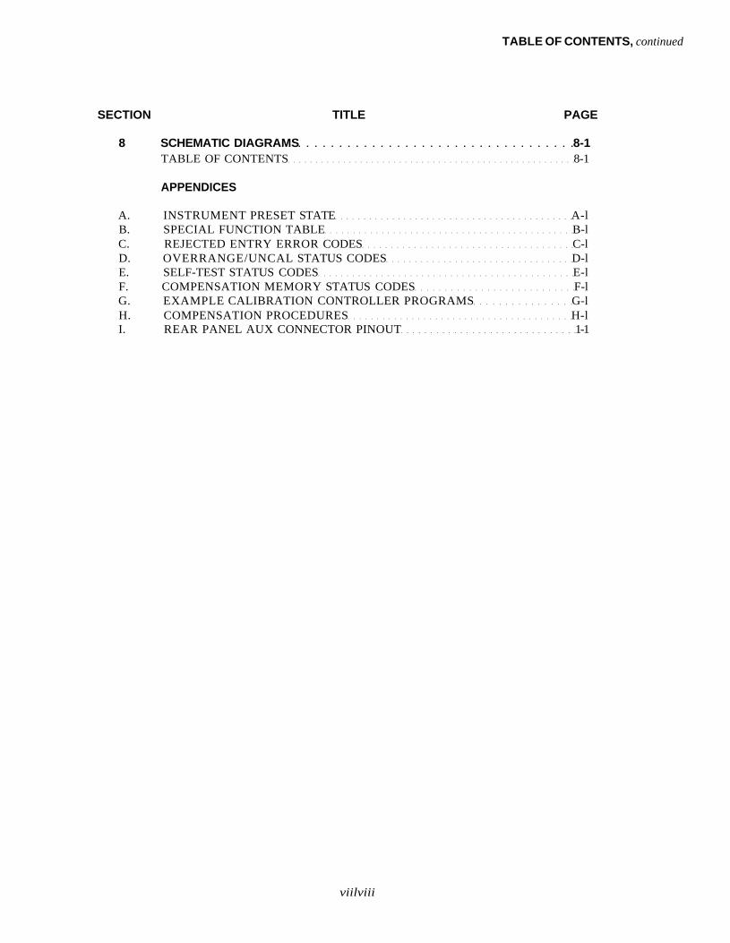
TABLE OF CONTENTS, continued
SECTION TITLE PAGE
8 SCHEMATIC DIAGRAMS 8-1TABLE OF CONTENTS 8-1
APPENDICES
A. INSTRUMENT PRESET STATE A-lB. SPECIAL FUNCTION TABLE B-lC. REJECTED ENTRY ERROR CODES C-lD. OVERRANGE/UNCAL STATUS CODES D-lE. SELF-TEST STATUS CODES E-lF. COMPENSATION MEMORY STATUS CODES F-lG. EXAMPLE CALIBRATION CONTROLLER PROGRAMS G-lH. COMPENSATION PROCEDURES H-lI. REAR PANEL AUX CONNECTOR PINOUT 1-1
viilviii

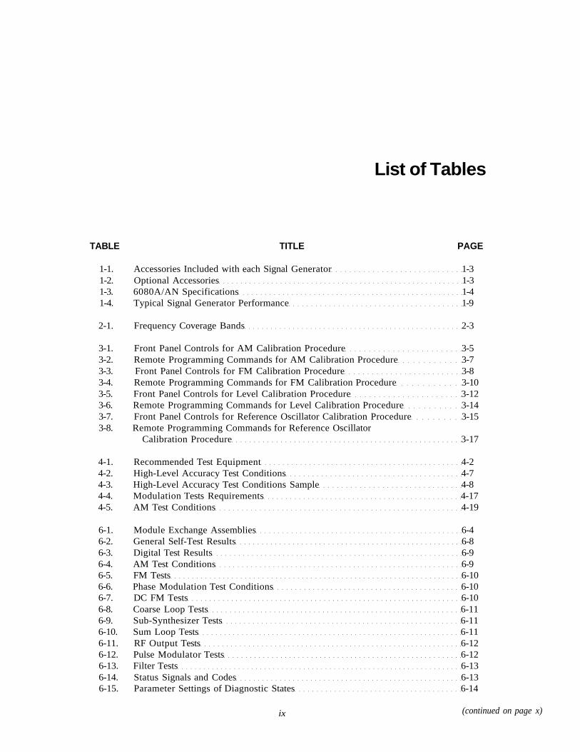
List of Tables
TABLE TITLE PAGE
1-1. Accessories Included with each Signal Generator 1-31-2. Optional Accessories 1-31-3. 6080A/AN Specifications 1-41-4. Typical Signal Generator Performance 1-9
2-1. Frequency Coverage Bands 2-3
3-1. Front Panel Controls for AM Calibration Procedure 3-53-2. Remote Programming Commands for AM Calibration Procedure 3-73-3. Front Panel Controls for FM Calibration Procedure 3-83-4. Remote Programming Commands for FM Calibration Procedure 3-103-5. Front Panel Controls for Level Calibration Procedure 3-123-6. Remote Programming Commands for Level Calibration Procedure 3-143-7. Front Panel Controls for Reference Oscillator Calibration Procedure 3-153-8. Remote Programming Commands for Reference Oscillator
Calibration Procedure 3-17
4-1. Recommended Test Equipment 4-24-2. High-Level Accuracy Test Conditions 4-74-3. High-Level Accuracy Test Conditions Sample 4-84-4. Modulation Tests Requirements 4-174-5. AM Test Conditions 4-19
6-1. Module Exchange Assemblies 6-46-2. General Self-Test Results 6-86-3. Digital Test Results 6-96-4. AM Test Conditions 6-96-5. FM Tests 6-106-6. Phase Modulation Test Conditions 6-106-7. DC FM Tests 6-106-8. Coarse Loop Tests 6-116-9. Sub-Synthesizer Tests 6-116-10. Sum Loop Tests 6-116-11. RF Output Tests 6-126-12. Pulse Modulator Tests 6-126-13. Filter Tests 6-136-14. Status Signals and Codes 6-136-15. Parameter Settings of Diagnostic States 6-14
ix (continued on page x)
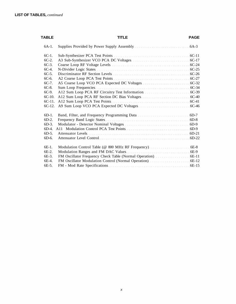
LIST OF TABLES, continued
TABLE TITLE PAGE
6A-1. Supplies Provided by Power Supply Assembly 6A-3
6C-1. Sub-Synthesizer PCA Test Points 6C-116C-2. A3 Sub-Synthesizer VCO PCA DC Voltages 6C-176C-3. Coarse Loop RF Voltage Levels 6C-246C-4. N-Divider Logic States 6C-256C-5. Discriminator RF Section Levels 6C-266C-6. A2 Coarse Loop PCA Test Points 6C-276C-7. A5 Coarse Loop VCO PCA Expected DC Voltages 6C-326C-8. Sum Loop Frequencies 6C-346C-9. A12 Sum Loop PCA RF Circuitry Test Information 6C-396C-10. A12 Sum Loop PCA RF Section DC Bias Voltages 6C-406C-11. A12 Sum Loop PCA Test Points 6C-416C-12. A9 Sum Loop VCO PCA Expected DC Voltages 6C-46
6D-1. Band, Filter, and Frequency Programming Data 6D-76D-2. Frequency Band Logic States 6D-86D-3. Modulator - Detector Nominal Voltages 6D-96D-4. A11 Modulation Control PCA Test Points 6D-96D-5. Attenuator Levels 6D-216D-6. Attenuator Level Control 6D-22
6E-1. Modulation Control Table (@ 800 MHz RF Frequency) 6E-86E-2. Modulation Ranges and FM DAC Values 6E-96E-3. FM Oscillator Frequency Check Table (Normal Operation) 6E-116E-4. FM Oscillator Modulation Control (Normal Operation) 6E-126E-5. FM - Mod Rate Specifications 6E-15
x
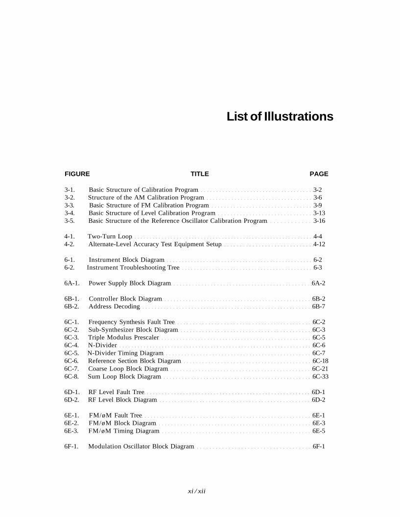
List of Illustrations
FIGURE TITLE PAGE
3-1. Basic Structure of Calibration Program 3-23-2. Structure of the AM Calibration Program 3-63-3. Basic Structure of FM Calibration Program 3-93-4. Basic Structure of Level Calibration Program 3-133-5. Basic Structure of the Reference Oscillator Calibration Program 3-16
4-1. Two-Turn Loop 4-44-2. Alternate-Level Accuracy Test Equipment Setup 4-12
6-1. Instrument Block Diagram 6-26-2. Instrument Troubleshooting Tree 6-3
6A-1. Power Supply Block Diagram 6A-2
6B-1. Controller Block Diagram 6B-26B-2. Address Decoding 6B-7
6C-1. Frequency Synthesis Fault Tree 6C-26C-2. Sub-Synthesizer Block Diagram 6C-36C-3. Triple Modulus Prescaler 6C-56C-4. N-Divider 6C-66C-5. N-Divider Timing Diagram 6C-76C-6. Reference Section Block Diagram 6C-186C-7. Coarse Loop Block Diagram 6C-216C-8. Sum Loop Block Diagram 6C-33
6D-1. RF Level Fault Tree 6D-16D-2. RF Level Block Diagram 6D-2
6E-1. FM/øM Fault Tree 6E-16E-2. FM/øM Block Diagram 6E-36E-3. FM/øM Timing Diagram 6E-5
6F-1. Modulation Oscillator Block Diagram 6F-1
xi / xii

Section 1Introduction and Specifications
INTRODUCTION 1-1.
The 6080A/AN Synthesized RF Signal Generator (also referred to throughout as the"signal generator") is a fully programmable, precision, synthesized signal generator.The 6080A/AN is designed for applications that require good modulation, frequencyaccuracy, and output level performance with excellent spectral purity. The signalgenerator is well suited for testing a wide variety of RF components and systemsincluding filters, amplifiers, mixers, and radios, particularly off-channel radio testing.
Specifications of the 6080A/AN are provided at the end of this section. The salientfeatures of the 6080A/AN are as follows:
• RF frequency range of 0.5 MHz to 1024 MHz in 1 Hz steps
• RF level range of +13 to -137 dBm in 0.1 dB steps
• Internal and External Modulation: AM, FM, and Pulse
• Internal 10 Hz to 100 kHz Synthesized Sine Wave Modulation Oscillator
• Fifty Storable and Recallable Memory Locations
• Standard IEEE-488 (GPIB) Interface, complying with ANSI/IEEE Standards488.1-1987 and 488.2-1987
• Closed-case calibration capabilities for Frequency Reference, AM, FM, andLevel.
UNPACKING THE SIGNAL GENERATOR 1-2.
The shipping container should include a 6080A/AN Synthesized RF Signal generator,an Operator Manual, a Service Manual, a line power cord and two BNC dust caps.Accessories ordered for the signal generator are shipped in a separate container.
1-1
INTRODUCTION AND SPECIFICATIONS
SAFETY 1-3.
This manual contains information, warnings, and cautions that should be followed toensure safe operation and to maintain the generator in a safe condition.
The signal generator is designed primarily for indoor use and may be operated intemperatures from 0 to 50° C without degradation of its safety.
WARNING
TO AVOID ELECTRIC SHOCK, USE A POWER CORD THAT HAS ATHREE-PRONG PLUG. IF THE PROPER POWER CORD IS NOT USED, THE6080A/AN CASE CAN DEVELOP AN ELECTRICAL POTENTIAL ABOVEEARTH GROUND.
WARNING
PIVOTING MODULE INSTRUCTIONS
IF NECESSARY DURING REPAIRS, PIVOT THE TOP (SYNTHESIZER)MODULE UP TO ALLOW ACCESS TO ALL PARTS OF THE SIGNALGENERATOR THE MODULE IS HEAVY AND CARE SHOULD BEEXERCISED. THE GAS STRUT IS PROVIDED FOR PROTECTION. CHECKTHE CORRECT OPERATION OF THE GAS STRUT BY NOTING THERESISTANCE TO RAPID CLOSING OF THE MODULE WHILE YOU FIRMLYGRASP THE MODULE BY THE HANDLE.
OPENING AND CLOSING INSTRUCTIONS ARE GIVEN BELOW AND AREREPEATED ON THE DECAL ON THE TOP FRONT OF THE SYNTHESIZERMODULE.
RAISING THE MODULE:
1. REMOVE THREE HOLD-DOWN SCREWS LOCATED ON THE SIDERAILS.
2. GRASP THE HANDLE AND LIFT UP.
3. LOCK IN THE UP POSITION BY INSTALLING ONE SCREW IN THE PROTRUDINGBOSS ON EACH SIDE RAIL.
LOWERING THE MODULE:
1. SUPPORT IN THE UP POSITION AND REMOVE TWO LOCK UP SCREWS.
2. GRASP THE HANDLE AND LOWER THE MODULE KEEPING YOUR HANDSCLEAR.
3. LOCK IN THE DOWN POSITION BY REINSTALLING THE THREE HOLD-DOWNSCREWS.
1-2
INTRODUCTION AND SPECIFICATIONS
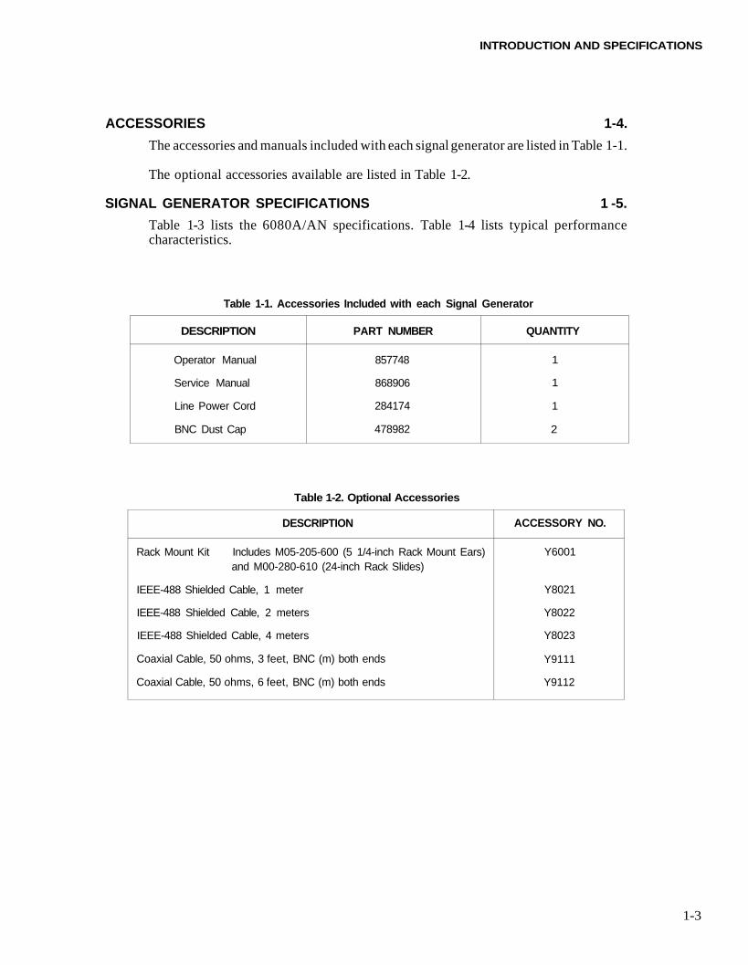
ACCESSORIES 1-4.
The accessories and manuals included with each signal generator are listed in Table 1-1.
The optional accessories available are listed in Table 1-2.
SIGNAL GENERATOR SPECIFICATIONS 1 -5.
Table 1-3 lists the 6080A/AN specifications. Table 1-4 lists typical performancecharacteristics.
Table 1-1. Accessories Included with each Signal Generator
DESCRIPTION
Operator Manual
Service Manual
Line Power Cord
BNC Dust Cap
PART NUMBER
857748
868906
284174
478982
QUANTITY
1
1
1
2
DESCRIPTION
Rack Mount Kit Includes M05-205-600 (5 1/4-inch Rack Mount Ears)and M00-280-610 (24-inch Rack Slides)
IEEE-488 Shielded Cable, 1 meter
IEEE-488 Shielded Cable, 2 meters
IEEE-488 Shielded Cable, 4 meters
Coaxial Cable, 50 ohms, 3 feet, BNC (m) both ends
Coaxial Cable, 50 ohms, 6 feet, BNC (m) both ends
ACCESSORY NO.
Y6001
Y8021
Y8022
Y8023
Y9111
Y9112
Table 1-2. Optional Accessories
1-3
INTRODUCTION AND SPECIFICATIONS
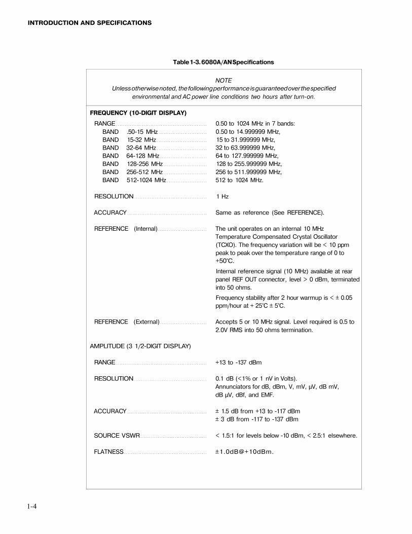
Table 1-3. 6080A/AN Specifications
NOTEUnless otherwise noted, the following performance is guaranteed over the specified
environmental and AC power line conditions two hours after turn-on.
FREQUENCY (10-DIGIT DISPLAY)
RANGE
BAND .50-15 MHzBAND 15-32 MHzBAND 32-64 MHzBAND 64-128 MHzBAND 128-256 MHzBAND 256-512 MHzBAND 512-1024 MHz
RESOLUTION
ACCURACY
REFERENCE (Internal)
REFERENCE (External)
AMPLITUDE (3 1/2-DIGIT DISPLAY)
RANGE
RESOLUTION
ACCURACY
SOURCE VSWR
FLATNESS
0.50 to 1024 MHz in 7 bands:0.50 to 14.999999 MHz,15 to 31.999999 MHz,32 to 63.999999 MHz,64 to 127.999999 MHz,128 to 255.999999 MHz,256 to 511.999999 MHz,512 to 1024 MHz.
1 Hz
Same as reference (See REFERENCE).
The unit operates on an internal 10 MHzTemperature Compensated Crystal Oscillator(TCXO). The frequency variation will be < 10 ppmpeak to peak over the temperature range of 0 to+50°C.
Internal reference signal (10 MHz) available at rearpanel REF OUT connector, level > 0 dBm, terminatedinto 50 ohms.
Frequency stability after 2 hour warmup is < ± 0.05ppm/hour at + 25°C ± 5°C.
Accepts 5 or 10 MHz signal. Level required is 0.5 to
2.0V RMS into 50 ohms termination.
+13 to -137 dBm
0.1 dB (<1% or 1 nV in Volts).Annunciators for dB, dBm, V, mV, μV, dB mV,dB μV, dBf, and EMF.
± 1.5 dB from +13 to -117 dBm± 3 dB from -117 to -137 dBm
< 1.5:1 for levels below -10 dBm, < 2.5:1 elsewhere.
±1.0dB@+10dBm.
1-4
INTRODUCTION AND SPECIFICATIONS
Table 1-3. 6080A/AN Specifications (cont)
1-5
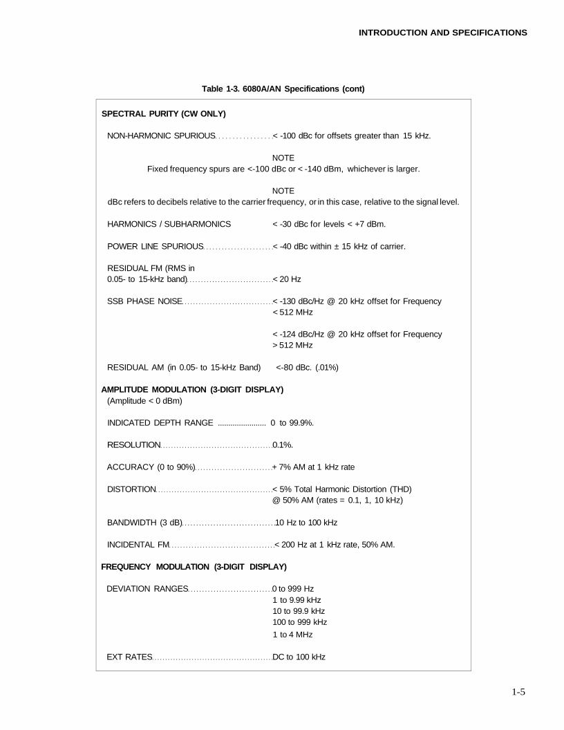
SPECTRAL PURITY (CW ONLY)
NON-HARMONIC SPURIOUS < -100 dBc for offsets greater than 15 kHz.
NOTEFixed frequency spurs are <-100 dBc or < -140 dBm, whichever is larger.
NOTEdBc refers to decibels relative to the carrier frequency, or in this case, relative to the signal level.
HARMONICS / SUBHARMONICS < -30 dBc for levels < +7 dBm.
POWER LINE SPURIOUS < -40 dBc within ± 15 kHz of carrier.
RESIDUAL FM (RMS in0.05- to 15-kHz band) < 20 Hz
SSB PHASE NOISE < -130 dBc/Hz @ 20 kHz offset for Frequency< 512 MHz
< -124 dBc/Hz @ 20 kHz offset for Frequency> 512 MHz
RESIDUAL AM (in 0.05- to 15-kHz Band) <-80 dBc. (.01%)
AMPLITUDE MODULATION (3-DIGIT DISPLAY)(Amplitude < 0 dBm)
INDICATED DEPTH RANGE ....................... 0 to 99.9%.
RESOLUTION 0.1%.
ACCURACY (0 to 90%) + 7% AM at 1 kHz rate
DISTORTION < 5% Total Harmonic Distortion (THD)@ 50% AM (rates = 0.1, 1, 10 kHz)
BANDWIDTH (3 dB) 10 Hz to 100 kHz
INCIDENTAL FM < 200 Hz at 1 kHz rate, 50% AM.
FREQUENCY MODULATION (3-DIGIT DISPLAY)
DEVIATION RANGES 0 to 999 Hz1 to 9.99 kHz10 to 99.9 kHz100 to 999 kHz
1 to 4 MHz
EXT RATES DC to 100 kHz
INTRODUCTION AND SPECIFICATIONS
Table 1-3. 6080A/AN Specifications (cont)
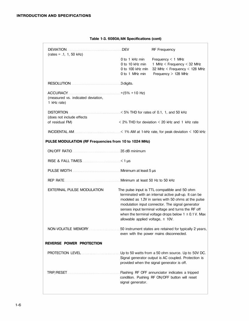
1-6
DEVIATION DEV RF Frequency(rates = .1, 1, 50 kHz)
0 to 1 kHz min Frequency < 1 MHz0 to 10 kHz min 1 MHz < Frequency < 32 MHz0 to 100 kHz mln 32 MHz < Frequency < 128 MHz0 to 1 MHz min Frequency > 128 MHz
RESOLUTION 3 digits.
ACCURACY +(5% +10 Hz)(measured vs. indicated deviation,1 kHz rate)
DISTORTION < 5% THD for rates of 0.1, 1, and 50 kHz
(does not include effects
of residual FM) < 2% THD for deviation < 20 kHz and 1 kHz rate
INCIDENTAL AM < 1% AM at 1-kHz rate, for peak deviation < 100 kHz
PULSE MODULATION (RF Frequencies from 10 to 1024 MHz)
ON/OFF RATIO 35 dB minimum
RISE & FALL TIMES < 1 μs
PULSE WIDTH Minimum at least 5 μs
REP RATE Minimum at least 50 Hz to 50 kHz
EXTERNAL PULSE MODULATION The pulse input is TTL compatible and 50 ohmterminated with an internal active pull-up. It can bemodeled as 1.2V in series with 50 ohms at the pulse
modulation input connector. The signal generator
senses input terminal voltage and turns the RF off
when the terminal voltage drops below 1 ± 0.1 V. Max
allowable applied voltage, ± 10V.
NON-VOLATILE MEMORY 50 instrument states are retained for typically 2 years,even with the power mains disconnected.
REVERSE POWER PROTECTION
PROTECTION LEVEL Up to 50 watts from a 50 ohm source. Up to 50V DC.
Signal generator output is AC coupled. Protection is
provided when the signal generator is off.
TRIP/RESET Flashing RF OFF annunciator indicates a trippedcondition. Pushing RF ON/OFF button will reset
signal generator.
INTRODUCTION AND SPECIFICATIONS
Table 1-3. 6080A/AN Specifications (cont)
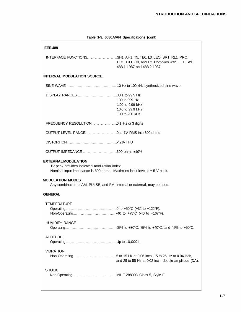
IEEE-488
INTERFACE FUNCTIONS SH1, AH1, T5, TE0, L3, LEO, SR1, RL1, PRO,DC1, DT1, C0, and E2. Complies with IEEE Std.488.1-1987 and 488.2-1987.
INTERNAL MODULATION SOURCE
SINE WAVE 10 Hz to 100 kHz synthesized sine wave.
DISPLAY RANGES 00.1 to 99.9 Hz100 to 999 Hz1.00 to 9.99 kHz10.0 to 99.9 kHz100 to 200 kHz
FREQUENCY RESOLUTION 0.1 Hz or 3 digits
OUTPUT LEVEL RANGE 0 to 1V RMS into 600 ohms
DISTORTION < 2% THD
OUTPUT IMPEDANCE 600 ohms ±10%
EXTERNAL MODULATION1V peak provides indicated modulation index.Nominal input impedance is 600 ohms. Maximum input level is ± 5 V peak.
MODULATION MODESAny combination of AM, PULSE, and FM, internal or external, may be used.
GENERAL
TEMPERATUREOperating 0 to +50°C (+32 to +122°F).Non-Operating -40 to +75°C (-40 to +167°F).
HUMIDITY RANGEOperating 95% to +30°C, 75% to +40°C, and 45% to +50°C.
ALTITUDEOperating Up to 10,000ft.
VIBRATIONNon-Operating 5 to 15 Hz at 0.06 inch, 15 to 25 Hz at 0.04 inch,
and 25 to 55 Hz at 0.02 inch, double amplitude (DA).
SHOCKNon-Operating MIL T 28800D Class 5, Style E.
1-7
INTRODUCTION AND SPECIFICATIONS
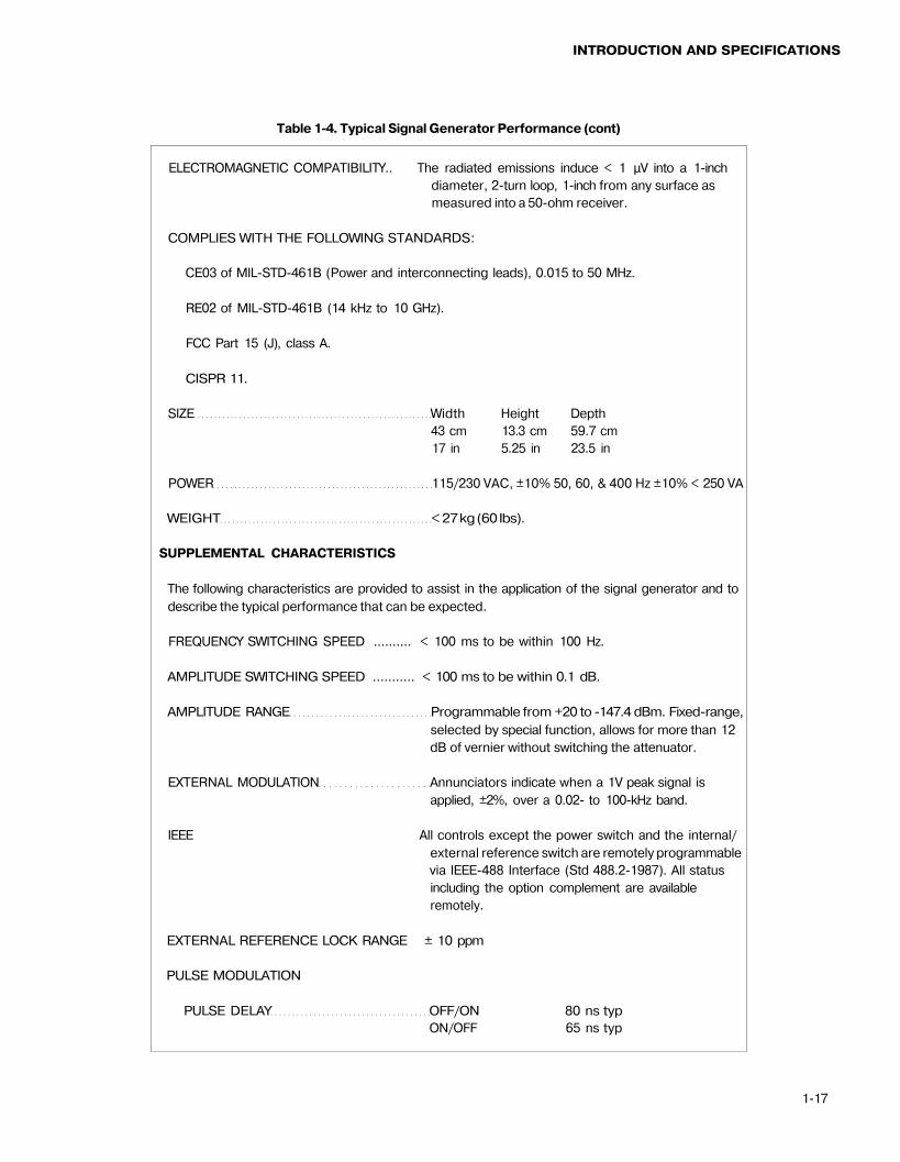
Table 1-3. 6080A/AN Specifications (cont)
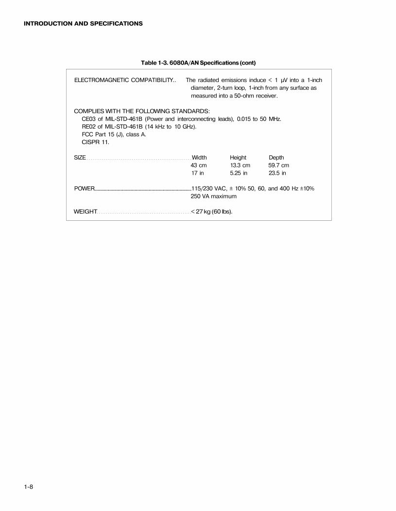
ELECTROMAGNETIC COMPATIBILITY.. The radiated emissions induce < 1 μV into a 1-inchdiameter, 2-turn loop, 1-inch from any surface as
measured into a 50-ohm receiver.
COMPLIES WITH THE FOLLOWING STANDARDS:CE03 of MIL-STD-461B (Power and interconnecting leads), 0.015 to 50 MHz.RE02 of MIL-STD-461B (14 kHz to 10 GHz).FCC Part 15 (J), class A.CISPR 11.
SIZE Width Height Depth43 cm 13.3 cm 59.7 cm17 in 5.25 in 23.5 in
POWER 115/230 VAC, ± 10% 50, 60, and 400 Hz ±10%250 VA maximum
WEIGHT < 27 kg (60 Ibs).
1-8
INTRODUCTION AND SPECIFICATIONS
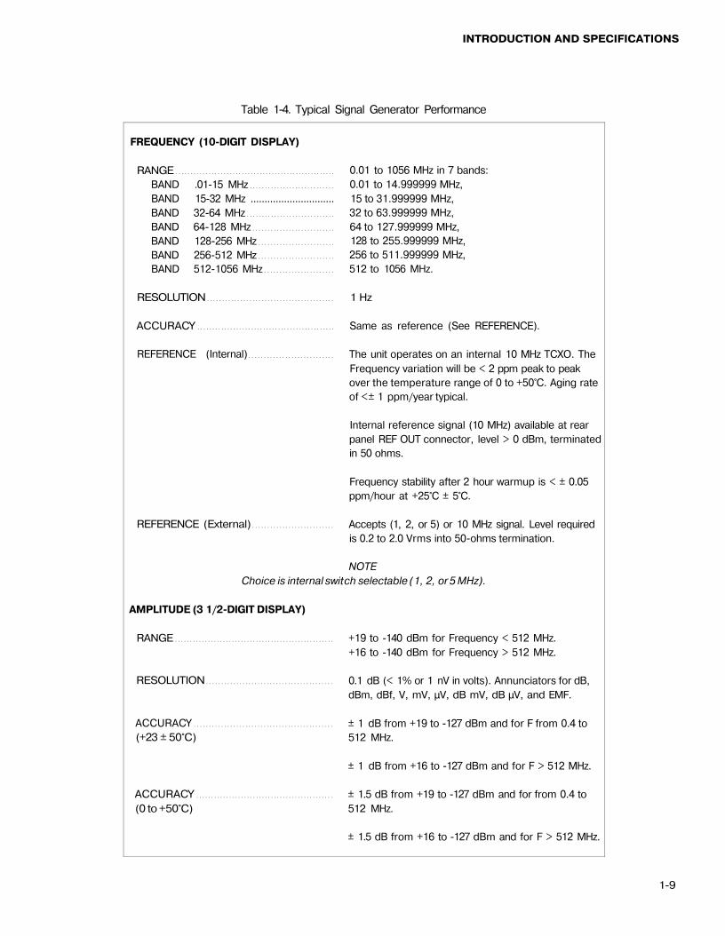
Table 1-4. Typical Signal Generator Performance
FREQUENCY (10-DIGIT DISPLAY)
RANGEBAND .01-15 MHzBAND 15-32 MHz ..............................BAND 32-64 MHzBAND 64-128 MHzBAND 128-256 MHzBAND 256-512 MHzBAND 512-1056 MHz
RESOLUTION
ACCURACY
REFERENCE (Internal)
REFERENCE (External)
Choice is internal swit
AMPLITUDE (3 1/2-DIGIT DISPLAY)
RANGE
RESOLUTION
ACCURACY(+23 ± 50°C)
ACCURACY
(0 to +50°C)
0.01 to 1056 MHz in 7 bands:0.01 to 14.999999 MHz,15 to 31.999999 MHz,32 to 63.999999 MHz,64 to 127.999999 MHz,128 to 255.999999 MHz,256 to 511.999999 MHz,512 to 1056 MHz.
1 Hz
Same as reference (See REFERENCE).
The unit operates on an internal 10 MHz TCXO. The
Frequency variation will be < 2 ppm peak to peakover the temperature range of 0 to +50°C. Aging rateof <± 1 ppm/year typical.
Internal reference signal (10 MHz) available at rearpanel REF OUT connector, level > 0 dBm, terminatedin 50 ohms.
Frequency stability after 2 hour warmup is < ± 0.05ppm/hour at +25°C ± 5°C.
Accepts (1, 2, or 5) or 10 MHz signal. Level requiredis 0.2 to 2.0 Vrms into 50-ohms termination.
NOTEch selectable (1, 2, or 5 MHz).
+19 to -140 dBm for Frequency < 512 MHz.+16 to -140 dBm for Frequency > 512 MHz.
0.1 dB (< 1% or 1 nV in volts). Annunciators for dB,dBm, dBf, V, mV, μV, dB mV, dB μV, and EMF.
± 1 dB from +19 to -127 dBm and for F from 0.4 to512 MHz.
± 1 dB from +16 to -127 dBm and for F > 512 MHz.
± 1.5 dB from +19 to -127 dBm and for from 0.4 to512 MHz.
± 1.5 dB from +16 to -127 dBm and for F > 512 MHz.
1-9
INTRODUCTION AND SPECIFICATIONS
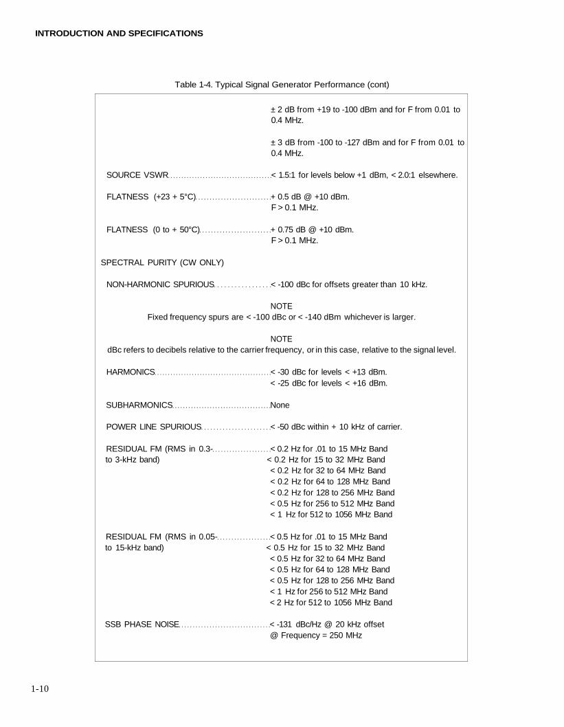
Table 1-4. Typical Signal Generator Performance (cont)
1-10
± 2 dB from +19 to -100 dBm and for F from 0.01 to0.4 MHz.
± 3 dB from -100 to -127 dBm and for F from 0.01 to0.4 MHz.
SOURCE VSWR < 1.5:1 for levels below +1 dBm, < 2.0:1 elsewhere.
FLATNESS (+23 + 5°C) + 0.5 dB @ +10 dBm.F > 0.1 MHz.
FLATNESS (0 to + 50°C) + 0.75 dB @ +10 dBm.F > 0.1 MHz.
SPECTRAL PURITY (CW ONLY)
NON-HARMONIC SPURIOUS < -100 dBc for offsets greater than 10 kHz.
NOTEFixed frequency spurs are < -100 dBc or < -140 dBm whichever is larger.
NOTEdBc refers to decibels relative to the carrier frequency, or in this case, relative to the signal level.
HARMONICS < -30 dBc for levels < +13 dBm.< -25 dBc for levels < +16 dBm.
SUBHARMONICS None
POWER LINE SPURIOUS < -50 dBc within + 10 kHz of carrier.
RESIDUAL FM (RMS in 0.3- < 0.2 Hz for .01 to 15 MHz Bandto 3-kHz band) < 0.2 Hz for 15 to 32 MHz Band
< 0.2 Hz for 32 to 64 MHz Band< 0.2 Hz for 64 to 128 MHz Band< 0.2 Hz for 128 to 256 MHz Band< 0.5 Hz for 256 to 512 MHz Band< 1 Hz for 512 to 1056 MHz Band
RESIDUAL FM (RMS in 0.05- < 0.5 Hz for .01 to 15 MHz Bandto 15-kHz band) < 0.5 Hz for 15 to 32 MHz Band
< 0.5 Hz for 32 to 64 MHz Band< 0.5 Hz for 64 to 128 MHz Band< 0.5 Hz for 128 to 256 MHz Band< 1 Hz for 256 to 512 MHz Band< 2 Hz for 512 to 1056 MHz Band
SSB PHASE NOISE < -131 dBc/Hz @ 20 kHz offset@ Frequency = 250 MHz
INTRODUCTION AND SPECIFICATIONS
Table 1-4. Typical Signal Generator Performance (cont)
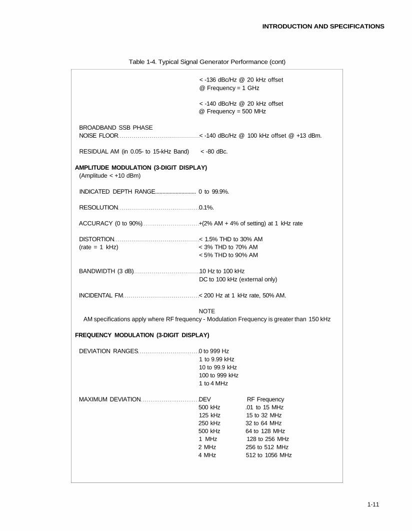
1-11
< -136 dBc/Hz @ 20 kHz offset@ Frequency = 1 GHz
< -140 dBc/Hz @ 20 kHz offset@ Frequency = 500 MHz
BROADBAND SSB PHASENOISE FLOOR < -140 dBc/Hz @ 100 kHz offset @ +13 dBm.
RESIDUAL AM (in 0.05- to 15-kHz Band) < -80 dBc.
AMPLITUDE MODULATION (3-DIGIT DISPLAY)(Amplitude < +10 dBm)
INDICATED DEPTH RANGE............................ 0 to 99.9%.
RESOLUTION 0.1%.
ACCURACY (0 to 90%) +(2% AM + 4% of setting) at 1 kHz rate
DISTORTION < 1.5% THD to 30% AM(rate = 1 kHz) < 3% THD to 70% AM
< 5% THD to 90% AM
BANDWIDTH (3 dB) 10 Hz to 100 kHzDC to 100 kHz (external only)
INCIDENTAL FM < 200 Hz at 1 kHz rate, 50% AM.
NOTEAM specifications apply where RF frequency - Modulation Frequency is greater than 150 kHz
FREQUENCY MODULATION (3-DIGIT DISPLAY)
DEVIATION RANGES 0 to 999 Hz1 to 9.99 kHz10 to 99.9 kHz100 to 999 kHz1 to 4 MHz
MAXIMUM DEVIATION DEV RF Frequency500 kHz .01 to 15 MHz125 kHz 15 to 32 MHz250 kHz 32 to 64 MHz500 kHz 64 to 128 MHz1 MHz 128 to 256 MHz2 MHz 256 to 512 MHz4 MHz 512 to 1056 MHz
INTRODUCTION AND SPECIFICATIONS
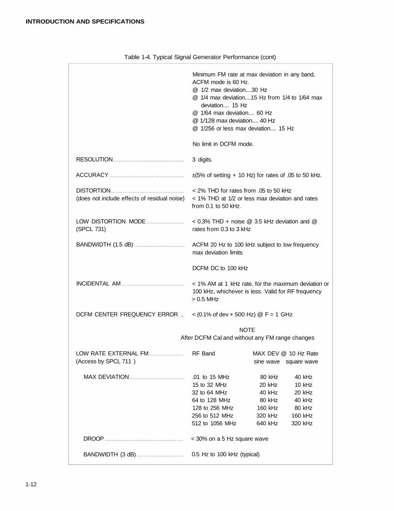
Table 1-4. Typical Signal Generator Performance (cont)
RESOLUTION
ACCURACY
DISTORTION(does not include effects of residual noise)
LOW DISTORTION MODE(SPCL 731)
BANDWIDTH (1.5 dB)
INCIDENTAL AM
DCFM CENTER FREQUENCY ERROR ..
Afte
LOW RATE EXTERNAL FM(Access by SPCL 711 )
MAX DEVIATION
DROOP
BANDWIDTH (3 dB)
Minimum FM rate at max deviation in any band,ACFM mode is 60 Hz.@ 1/2 max deviation....30 Hz@ 1/4 max deviation....15 Hz from 1/4 to 1/64 max
deviation.... 15 Hz@ 1/64 max deviation.... 60 Hz@ 1/128 max deviation.... 40 Hz@ 1/256 or less max deviation.... 15 Hz
No limit in DCFM mode.
3 digits.
±(5% of setting + 10 Hz) for rates of .05 to 50 kHz.
< 2% THD for rates from .05 to 50 kHz< 1% THD at 1/2 or less max deviation and ratesfrom 0.1 to 50 kHz.
< 0.3% THD + noise @ 3.5 kHz deviation and @rates from 0.3 to 3 kHz
ACFM 20 Hz to 100 kHz subject to low frequencymax deviation limits
DCFM DC to 100 kHz
< 1% AM at 1 kHz rate, for the maximum deviation or100 kHz, whichever is less. Valid for RF frequency> 0.5 MHz
< (0.1% of dev + 500 Hz) @ F = 1 GHz
NOTEr DCFM Cal and without any FM range changes
RF Band MAX DEV @ 10 Hz Ratesine wave square wave
.01 to 15 MHz 80 kHz 40 kHz15 to 32 MHz 20 kHz 10 kHz32 to 64 MHz 40 kHz 20 kHz64 to 128 MHz 80 kHz 40 kHz128 to 256 MHz 160 kHz 80 kHz256 to 512 MHz 320 kHz 160 kHz512 to 1056 MHz 640 kHz 320 kHz
< 30% on a 5 Hz square wave
0.5 Hz to 100 kHz (typical)
1-12
INTRODUCTION AND SPECIFICATIONS
Table 1-4. Typical Signal Generator Performance (cont)
1-13
MAX DC INPUT
INCIDENTAL AM
FM specificRF FrequencyRF Frequency
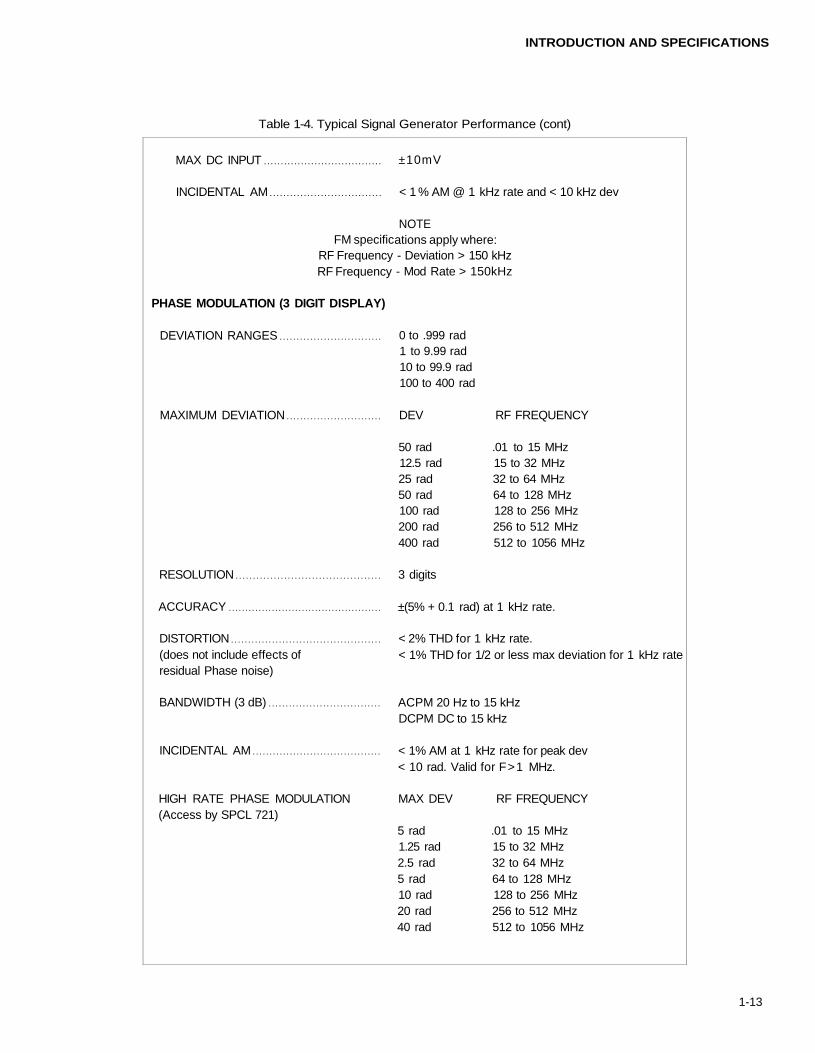
PHASE MODULATION (3 DIGIT DISPLAY)
DEVIATION RANGES
MAXIMUM DEVIATION
RESOLUTION
ACCURACY
DISTORTION(does not include effects ofresidual Phase noise)
BANDWIDTH (3 dB)
INCIDENTAL AM
HIGH RATE PHASE MODULATION(Access by SPCL 721)
±10mV
< 1 % AM @ 1 kHz rate and < 10 kHz dev
NOTEations apply where:- Deviation > 150 kHz- Mod Rate > 150kHz
0 to .999 rad1 to 9.99 rad10 to 99.9 rad100 to 400 rad
DEV RF FREQUENCY
50 rad .01 to 15 MHz12.5 rad 15 to 32 MHz25 rad 32 to 64 MHz50 rad 64 to 128 MHz100 rad 128 to 256 MHz200 rad 256 to 512 MHz400 rad 512 to 1056 MHz
3 digits
±(5% + 0.1 rad) at 1 kHz rate.
< 2% THD for 1 kHz rate.< 1% THD for 1/2 or less max deviation for 1 kHz rate
ACPM 20 Hz to 15 kHzDCPM DC to 15 kHz
< 1% AM at 1 kHz rate for peak dev< 10 rad. Valid for F>1 MHz.
MAX DEV RF FREQUENCY
5 rad .01 to 15 MHz1.25 rad 15 to 32 MHz2.5 rad 32 to 64 MHz5 rad 64 to 128 MHz10 rad 128 to 256 MHz20 rad 256 to 512 MHz40 rad 512 to 1056 MHz
INTRODUCTION AND SPECIFICATIONS
Table 1-4. Typical Signal Generator Performance (cont)
1-14
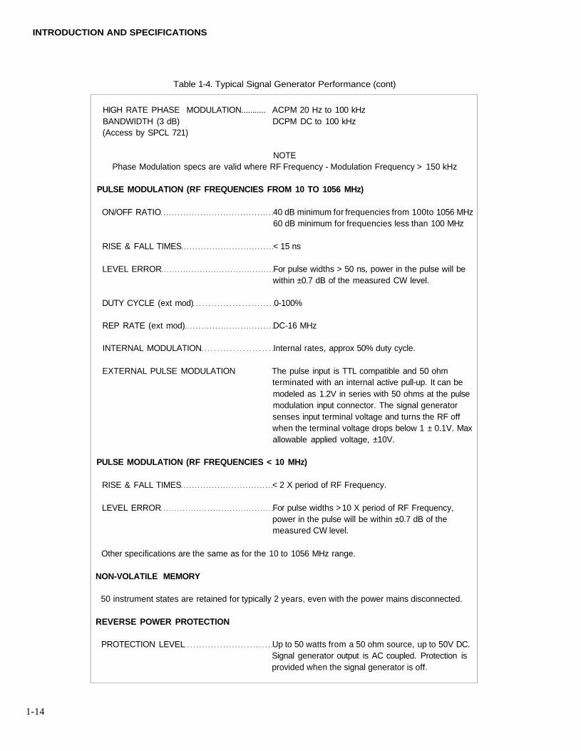
HIGH RATE PHASE MODULATION........... ACPM 20 Hz to 100 kHzBANDWIDTH (3 dB) DCPM DC to 100 kHz(Access by SPCL 721)
NOTEPhase Modulation specs are valid where RF Frequency - Modulation Frequency > 150 kHz
PULSE MODULATION (RF FREQUENCIES FROM 10 TO 1056 MHz)
ON/OFF RATIO 40 dB minimum for frequencies from 100to 1056 MHz60 dB minimum for frequencies less than 100 MHz
RISE & FALL TIMES < 15 ns
LEVEL ERROR For pulse widths > 50 ns, power in the pulse will bewithin ±0.7 dB of the measured CW level.
DUTY CYCLE (ext mod) 0-100%
REP RATE (ext mod) DC-16 MHz
INTERNAL MODULATION Internal rates, approx 50% duty cycle.
EXTERNAL PULSE MODULATION The pulse input is TTL compatible and 50 ohmterminated with an internal active pull-up. It can bemodeled as 1.2V in series with 50 ohms at the pulsemodulation input connector. The signal generatorsenses input terminal voltage and turns the RF offwhen the terminal voltage drops below 1 ± 0.1V. Maxallowable applied voltage, ±10V.
PULSE MODULATION (RF FREQUENCIES < 10 MHz)
RISE & FALL TIMES < 2 X period of RF Frequency.
LEVEL ERROR For pulse widths > 10 X period of RF Frequency,power in the pulse will be within ±0.7 dB of themeasured CW level.
Other specifications are the same as for the 10 to 1056 MHz range.
NON-VOLATILE MEMORY
50 instrument states are retained for typically 2 years, even with the power mains disconnected.
REVERSE POWER PROTECTION
PROTECTION LEVEL Up to 50 watts from a 50 ohm source, up to 50V DC.Signal generator output is AC coupled. Protection isprovided when the signal generator is off.
INTRODUCTION AND SPECIFICATIONS
Table 1-4. Typical Signal Generator Performance (cont)
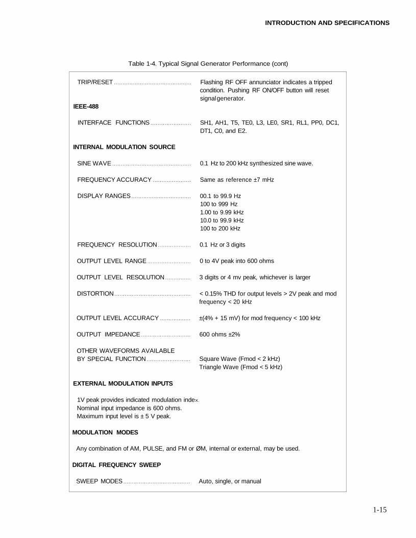
TRIP/RESET
IEEE-488
INTERFACE FUNCTIONS
INTERNAL MODULATION SOURCE
SINE WAVE
FREQUENCY ACCURACY
DISPLAY RANGES
FREQUENCY RESOLUTION
OUTPUT LEVEL RANGE
OUTPUT LEVEL RESOLUTION
DISTORTION
OUTPUT LEVEL ACCURACY
OUTPUT IMPEDANCE
OTHER WAVEFORMS AVAILABLEBY SPECIAL FUNCTION
EXTERNAL MODULATION INPUTS
1V peak provides indicated modulation indeNominal input impedance is 600 ohms.Maximum input level is ± 5 V peak.
MODULATION MODES
Any combination of AM, PULSE, and FM or
DIGITAL FREQUENCY SWEEP
SWEEP MODES
Flashing RF OFF annunciator indicates a trippedcondition. Pushing RF ON/OFF button will resetsignal generator.
SH1, AH1, T5, TE0, L3, LE0, SR1, RL1, PP0, DC1,DT1, C0, and E2.
0.1 Hz to 200 kHz synthesized sine wave.
Same as reference ±7 mHz
00.1 to 99.9 Hz100 to 999 Hz1.00 to 9.99 kHz10.0 to 99.9 kHz100 to 200 kHz
0.1 Hz or 3 digits
0 to 4V peak into 600 ohms
3 digits or 4 mv peak, whichever is larger
< 0.15% THD for output levels > 2V peak and modfrequency < 20 kHz
±(4% + 15 mV) for mod frequency < 100 kHz
600 ohms ±2%
Square Wave (Fmod < 2 kHz)Triangle Wave (Fmod < 5 kHz)
X.
ØM, internal or external, may be used.
Auto, single, or manual
1-15
INTRODUCTION AND SPECIFICATIONS
Table 1-4. Typical Signal Generator Performance (cont)
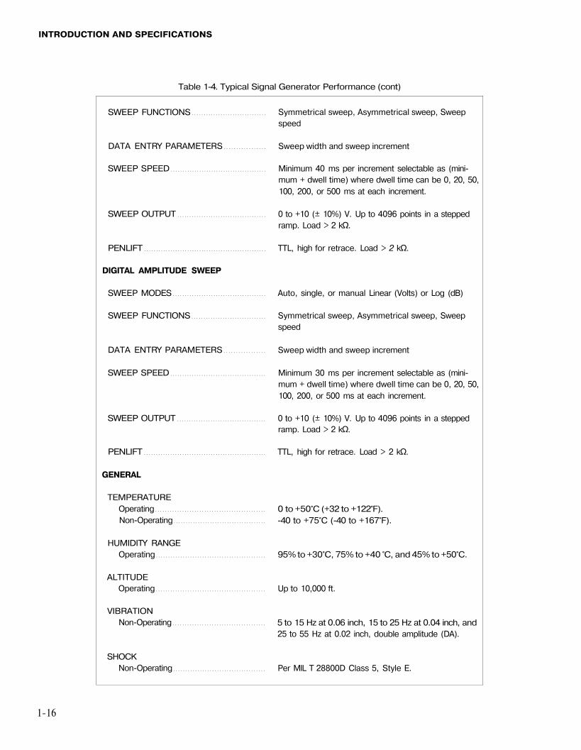
SWEEP FUNCTIONS
DATA ENTRY PARAMETERS
SWEEP SPEED
SWEEP OUTPUT
PENLIFT
DIGITAL AMPLITUDE SWEEP
SWEEP MODES
SWEEP FUNCTIONS
DATA ENTRY PARAMETERS
SWEEP SPEED
SWEEP OUTPUT
PENLIFT
GENERAL
TEMPERATURE
Operating
Non-Operating
HUMIDITY RANGEOperating
ALTITUDEOperating
VIBRATIONNon-Operating
SHOCKNon-Operating
Symmetrical sweep, Asymmetrical sweep, Sweepspeed
Sweep width and sweep increment
Minimum 40 ms per increment selectable as (mini-mum + dwell time) where dwell time can be 0, 20, 50,
100, 200, or 500 ms at each increment.
0 to +10 (± 10%) V. Up to 4096 points in a steppedramp. Load > 2 kΩ.
TTL, high for retrace. Load > 2 kΩ.
Auto, single, or manual Linear (Volts) or Log (dB)
Symmetrical sweep, Asymmetrical sweep, Sweepspeed
Sweep width and sweep increment
Minimum 30 ms per increment selectable as (mini-mum + dwell time) where dwell time can be 0, 20, 50,
100, 200, or 500 ms at each increment.
0 to +10 (± 10%) V. Up to 4096 points in a steppedramp. Load > 2 kΩ.
TTL, high for retrace. Load > 2 kΩ.
0 to +50°C (+32 to +122°F).
-40 to +75°C (-40 to +167°F).
95% to +30°C, 75% to +40 °C, and 45% to +50°C.
Up to 10,000 ft.
5 to 15 Hz at 0.06 inch, 15 to 25 Hz at 0.04 inch, and25 to 55 Hz at 0.02 inch, double amplitude (DA).
Per MIL T 28800D Class 5, Style E.
1-16
INTRODUCTION AND SPECIFICATIONS
Table 1-4. Typical Signal Generator Performance (cont)
ELECTROMAGNETIC COMPATIBILITY.. The radiated emissions induce < 1 μV into a 1-inchdiameter, 2-turn loop, 1-inch from any surface asmeasured into a 50-ohm receiver.
COMPLIES WITH THE FOLLOWING STANDARDS:
CE03 of MIL-STD-461B (Power and interconnecting leads), 0.015 to 50 MHz.
RE02 of MIL-STD-461B (14 kHz to 10 GHz).
FCC Part 15 (J), class A.
CISPR 11.
SIZE Width Height Depth43 cm 13.3 cm 59.7 cm17 in 5.25 in 23.5 in
POWER 115/230 VAC, ±10% 50, 60, & 400 Hz ±10% < 250 VA
WEIGHT < 27 kg (60 Ibs).
SUPPLEMENTAL CHARACTERISTICS
The following characteristics are provided to assist in the application of the signal generator and to
describe the typical performance that can be expected.
FREQUENCY SWITCHING SPEED .......... < 100 ms to be within 100 Hz.
AMPLITUDE SWITCHING SPEED ........... < 100 ms to be within 0.1 dB.
AMPLITUDE RANGE Programmable from +20 to -147.4 dBm. Fixed-range,
selected by special function, allows for more than 12dB of vernier without switching the attenuator.
EXTERNAL MODULATION Annunciators indicate when a 1V peak signal is
applied, ±2%, over a 0.02- to 100-kHz band.
IEEE All controls except the power switch and the internal/
external reference switch are remotely programmablevia IEEE-488 Interface (Std 488.2-1987). All statusincluding the option complement are availableremotely.
EXTERNAL REFERENCE LOCK RANGE ± 10 ppm
PULSE MODULATION
PULSE DELAY OFF/ON 80 ns typON/OFF 65 ns typ
1-17

INTRODUCTION AND SPECIFICATIONS
Table 1-4. Typical Signal Generator Performance (cont)
DCFM DRIFT 3 ppm/hr for < 1/16 max deviation(after 2 hour warmup and at constant 8 ppm/hr for > 1/16 max deviationtemperature)
1-18
Section 2Theory of Operation
INTRODUCTION 2-1.
Section 2 of this manual provides a basic description of the 6080A/AN SynthesizedSignal Generator (also referred to throughout as the "signal generator"). Three majortopics are covered:
• General Description
Briefly explains the functions and components of the four major sections of theGenerator.
• Functional Description
Describes the functional blocks of the signal generator and their relations to themain output parameters: amplitude, frequency, and modulation.
• Digital Controller Software Description
Describes the software and how it affects the hardware.
GENERAL DESCRIPTION 2-2.
The 6080A/AN Synthesized Signal Generator has four major sections:
• The front panel section includes the keyboard and display for local control.
• The upper (synthesizer) module section includes the coarse and fine loopsynthesized signals and the synthesized modulation oscillator.
• The lower (output) module includes the sum loop, FM oscillator, and the level,modulation, and control circuits.
• The rear panel section includes the power supply, cooling fan, and assortedexternal connectors.
2-1
THEORY OF OPERATION
Front Panel Section 2-3.
The front panel section of the signal generator provides the operator interface,including the primary controls, connectors, and indicators. All front panel keys anddisplays (except the power switch that directly controls the power supply) aremonitored and handled by the A13 Controller PCA, which is located in the outputmodule section.
Upper/Lower Module Sections 2-4.
The two module sections are multi-compartmented, shielded enclosures that containthe circuits that generate the instrument stimulus functions: frequency, modulation,and amplitude. These enclosures provide the necessary circuit-to-circuit isolation toprevent the generation of spurious signals. The enclosures serve to isolate the generatorcircuits from the outside environment.
Rear Panel Section 2-5.
The rear panel section includes the power supply, the cooling fan, various externalconnectors, and the IEEE-488 Interface connector.
FUNCTIONAL DESCRIPTION 2-6.
The key functional blocks of the signal generator (described in the followingparagraphs) are:
FrequencyFrequency modulationPhase modulationLevelAmplitude modulationPulse modulationInternal modulation oscillatorPower supplySoftware.
Frequency 2-7.
The output frequency (Fo) is programmable with 1-Hz resolution from 0.01 MHz to1056 MHz. The band controls are programmed in seven bands that are determined bythe output frequency (Fo). A coarse loop and sub-synthesizer frequency aredetermined for each band.
The programming of the coarse loop steering digital-to-analog converter (DAC),compensation DAC, and VCO control bits are determined from the coarse loopfrequency and the instrument-specific compensation data.
The programming of the sub-synthesizer compensation DAC is determined from thesub-synthesizer frequency and the instrument-specific compensation data.
The programming of the sum loop steering and compensation DACs are derived fromthe output frequency and the instrument-specific compensation data.
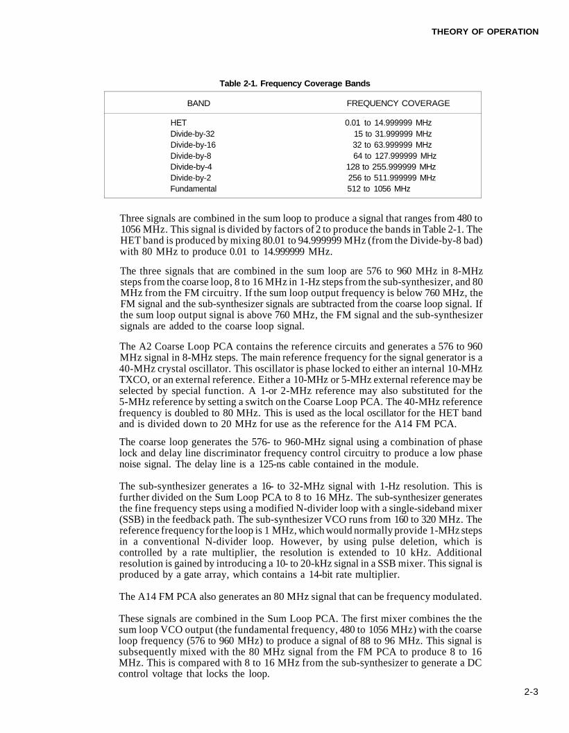
The 0.01- MHz to 1056-MHz frequency coverage is divided into the seven bandsshown in Table 2-1.
2-2
THEORY OF OPERATION
Table 2-1. Frequency Coverage Bands
BAND FREQUENCY COVERAGE
HET 0.01 to 14.999999 MHzDivide-by-32 15 to 31.999999 MHzDivide-by-16 32 to 63.999999 MHzDivide-by-8 64 to 127.999999 MHzDivide-by-4 128 to 255.999999 MHzDivide-by-2 256 to 511.999999 MHzFundamental 512 to 1056 MHz
Three signals are combined in the sum loop to produce a signal that ranges from 480 to1056 MHz. This signal is divided by factors of 2 to produce the bands in Table 2-1. TheHET band is produced by mixing 80.01 to 94.999999 MHz (from the Divide-by-8 bad)with 80 MHz to produce 0.01 to 14.999999 MHz.
The three signals that are combined in the sum loop are 576 to 960 MHz in 8-MHzsteps from the coarse loop, 8 to 16 MHz in 1-Hz steps from the sub-synthesizer, and 80MHz from the FM circuitry. If the sum loop output frequency is below 760 MHz, theFM signal and the sub-synthesizer signals are subtracted from the coarse loop signal. Ifthe sum loop output signal is above 760 MHz, the FM signal and the sub-synthesizersignals are added to the coarse loop signal.
The A2 Coarse Loop PCA contains the reference circuits and generates a 576 to 960MHz signal in 8-MHz steps. The main reference frequency for the signal generator is a40-MHz crystal oscillator. This oscillator is phase locked to either an internal 10-MHzTXCO, or an external reference. Either a 10-MHz or 5-MHz external reference may beselected by special function. A 1-or 2-MHz reference may also substituted for the5-MHz reference by setting a switch on the Coarse Loop PCA. The 40-MHz referencefrequency is doubled to 80 MHz. This is used as the local oscillator for the HET bandand is divided down to 20 MHz for use as the reference for the A14 FM PCA.
The coarse loop generates the 576- to 960-MHz signal using a combination of phaselock and delay line discriminator frequency control circuitry to produce a low phasenoise signal. The delay line is a 125-ns cable contained in the module.
The sub-synthesizer generates a 16- to 32-MHz signal with 1-Hz resolution. This isfurther divided on the Sum Loop PCA to 8 to 16 MHz. The sub-synthesizer generatesthe fine frequency steps using a modified N-divider loop with a single-sideband mixer(SSB) in the feedback path. The sub-synthesizer VCO runs from 160 to 320 MHz. Thereference frequency for the loop is 1 MHz, which would normally provide 1-MHz stepsin a conventional N-divider loop. However, by using pulse deletion, which iscontrolled by a rate multiplier, the resolution is extended to 10 kHz. Additionalresolution is gained by introducing a 10- to 20-kHz signal in a SSB mixer. This signal isproduced by a gate array, which contains a 14-bit rate multiplier.
The A14 FM PCA also generates an 80 MHz signal that can be frequency modulated.
These signals are combined in the Sum Loop PCA. The first mixer combines the thesum loop VCO output (the fundamental frequency, 480 to 1056 MHz) with the coarseloop frequency (576 to 960 MHz) to produce a signal of 88 to 96 MHz. This signal issubsequently mixed with the 80 MHz signal from the FM PCA to produce 8 to 16MHz. This is compared with 8 to 16 MHz from the sub-synthesizer to generate a DCcontrol voltage that locks the loop.
2-3
THEORY OF OPERATION
Frequency Modulation 2-8.
Frequency modulation (FM) is programmable with three digits of resolution in sixranges. The deviation is programmed using the 12-bit FM DAC and three FM rangebits. The FM DAC and range settings are dependent on the programmed deviationand the RF output frequency. The FM DAC and FM Range settings for eachfrequency band and FM deviation range are shown in Table 6E-2 in Section 6E. TheFM/øM modes are selected by the control bit PMODL.
The maximum programmable FM deviation is dependent on the RF outputfrequency. FM deviations up to 4 MHz may be entered regardless of the outputfrequency. However, the STATUS indicator is flashed and the FM DAC is clamped atfull scale if the entry is beyond the allowed upper limit for that frequency band. Themaximum programmable deviation in each frequency band is depicted in Section 4C,"Modulation" in the Operators Manual.
The FM oscillator loop runs at 80 MHz with several modes of operation. In the lowdeviation, low noise mode, the oscillator runs with the highest Q. As deviation isincreased, a linearizer is added to maintain low distortion, which somewhat reducesspectral purity. At higher deviations, the tuning sensitivity of the oscillator isincreased, again causing a somewhat higher phase noise. At this deviation, thelinearizer is used to maintain low distortion.
The phase lock circuit runs off of various reference frequencies depending on thedeviation selected. To provide a large amount of deviation at low rates, a very widerange phase detector is used in the wide deviation ACFM mode. Full deviation can beused down to an FM rate of 100 Hz. An alternate mode of operation that uses thelowest reference phase detector frequency and the wide range phase detector for alldeviations will allow very low modulation rates for less than maximum deviation.
In DCFM mode, full deviation can be used down to DC levels. The generator is not,however locked to the main timebase in this mode. When DCFM is enabled, the FMoscillator's center frequency is set to the previous locked center frequency ±1 kHz byautomatic zeroing circuitry in conjunction with the software routine.
Phase Modulation 2-9.
Phase modulation (øM) is programmable with three digits of resolution in six ranges.Phase modulation is internally normalized to 10 kHz, then programmed as FMdeviation. The øM index is multiplied by 10 kHz (regardless of the modulationfrequency) to get the "equivalent" FM deviation. Refer to Table 6E-2 (Section 6E) todetermine the FM DAC and range settings from this "equivalent" FM deviation.
The maximum programmable phase modulation deviation is dependent on the RFoutput frequency. Phase modulation deviations up to 400 radians may be enteredregardless of the output frequency. However, the STATUS indicator is flashed and theFM DAC is clamped at full scale if the entry is beyond the allowed upper limit for thatfrequency band. The maximum programmable phase modulation deviation in eachfrequency band is depicted in Section 4C, "Modulation", of the Operators Manual.
Phase modulation is achieved by reconfiguring the modulation circuits to cause a truephase modulation response for both internal and external modulation inputs. Thedisplay is correspondingly changed to indicate deviation in radians. Two modes areavailable: large deviation at a limited bandwidth and limited deviation for higher ratebandwidth.
2-4
THEORY OF OPERATION
Output/Level Control 2-10.
Level control is provided by two separate circuits: a step attenuator and a vernier levelDAC. The A20 Attenuator/RPP Assembly provides coarse level control in 6.02-dBsteps. Fine level control is provided by a vernier level DAC that varies the leveling-loopcontrol voltage. The controller microprocessor automatically controls the stepattenuator and the vernier level DAC. The microprocessor also applies level correctionto compensate for the signal generator frequency response.
Each signal generator has level correction data for both the A8 Output PCA and theA20 Attenuator/RPP Assembly. The level correction data is stored in the compensa-tion memory located on the A13 Controller PCA. The level correction data is based onthe measurements of each assembly during level compensation of the signal generator.
The level correction data is applied only to the vernier level DAC and does not affectthe coarse level control provided by the Attenuator/RPP Assembly. In other words,all signal generators have the same attenuator pads inserted at a selected level eventhough the correction data is different for each signal generator.
To improve level accuracy in relation to temperature, the signal generator uses asoftware temperature-compensation technique. This technique uses data that is thesame for all signal generators.
Amplitude Modulation 2-11.
The signal generator allows amplitude modulation depth programming from 0 to99.9% with 0.1% resolution. Amplitude modulation depth is programmed using the12-bit AM DAC. A nominal setting of 2997 on the AM DAC corresponds to 99.9%AM depth.
The output of the level DAC is the leveling loop-control voltage. The signal generatoroutput signal is amplitude modulated by varying this control voltage with themodulating signal. A 1V peak modulating signal from the internal modulationoscillator or from the external MOD INPUT connector is applied to the AM DAC (amultiplying digital-to-analog converter). The multiplying factor of this DAC,corresponding to the programmed percentage of modulation, is calculated by the A13Controller PCA.
The modulation signal from the AM DAC is summed with a fixed DC referencevoltage. The composite signal (DC plus modulation) is applied to the level DAC (alevel control-multiplying DAC). The multiplying factor for this DAC is also handledby the A13 Controller PCA and corresponds to the programmed signal level. Themultipling factor also includes the level correction information stored in thecompensation memory.
The operation of the ALC loop causes the amplitude of the RF signal to conform tothis varying control voltage, thus causing amplitude modulation of the signalgenerator output.
Pulse Modulation 2-12.
Pulse modulation is accomplished by a single-pole single-throw GaAs FET switchlocated at the input to the output amplifier. This switch can be driven by the internalmodulation oscillator or by an external signal. The GaAs FET switch provides a veryfast and high ON/OFF ratio RF pulse.
2-5
THEORY OF OPERATION
Internal Modulation Oscillator 2-13.
The modulation oscillator is made up of two sections; a periodic wave generator and apulse generator. Both functions are implemented in a custom integrated circuit and aresynthesized from the main reference frequency source of the 6080A/AN.
The periodic wave generator frequency can be set from 0.1 Hz to 200 kHz withresolution of 0.1 Hz. It is the modulation source for the internal AM, FM, øM, andpulse functions. The oscillator is based on an algorithmic wave generation method,which provides a very accurate and stable signal source of high purity and lowharmonic distortion level. The main function of this system is implemented in a customintegrated circuit. The waveform data is stored in two EPROMs.
In the pulse generation mode, frequency can be set from 10 Hz to 200 kHz, whichresults in a pulse period of 0.1 s through 500 us. The pulse width can be set from 100 nsto 100 ms, with resolution of 100 ns.
Power Supply Description 2-14.
The power supply is a linear design providing + 15V, -15V, +5V, +37V, +30V, +24V,+23.4V DC, and 6V AC to the signal generator. All the power supplies are series-passregulated except the 6V AC display filament supply. A fuse/filter/line-voltage selectorallows the signal generator to operate from 115 or 230V AC.
DIGITAL CONTROLLER SOFTWARE DESCRIPTION 2-15.
The signal generator software is executed on an 68HCOOO microprocessor located inthe A13 Controller PCA. The instrument program is stored in 256K bytes of ROM.The program stack and RAM variables are stored in 16K bytes of static RAM. Abattery-backed CMOS RAM contains 4K bytes of non-volatile memory for frontpanel setups, and 4K bytes of non-volatile calibration/compensation data. An 8K byteEEPROM contains a redundant copy of the calibration/compensation data. Thesoftware provides the following general functions:
• Services the front panel and the IEEE-488 Interface.
• Configures the hardware to produce the required output, then applies calibrationand compensation data to optimize the performance.
• Implements a set of self-test and diagnostic functions.
User Interface 2-16.
The software is implemented with a simple operating system that allows several tasksto operate in a round-robin fashion. Input and output to both the front panel and theIEEE-488 Interface execute at a higher priority and are handled as interrupt routines.
At power-on, the software performs a self-test and initializes both the RAM and theRF hardware. Four tasks are continuously in operation:
• Diagnostic service task• Front panel Key task• Knob task• IEEE-488 task
2-6
THEORY OF OPERATION
The diagnostic service task monitors the instrument status signals. The front panel keytask, knob task and IEEE-488 task process user input. A fifth task controls the RFoutput when a frequency or amplitude sweep is active. A sixth task is activated onlywhen needed to process certain STATUS (out-of-range or malfunction) or REJENTRY (rejected entry) conditions that cause the display to flash. A seventh task isactivated when the automatic user compensation procedures have been initiated.
Calibration/Compensation Memory 2-17.
The calibration/compensation memory contains the instrument-specific compensationdata for the coarse loop compensation DAC, coarse loop steering DAC, sum loopcompensation DAC, sum loop steering DAC, sub-synthesizer compensation DAC,the Output assembly, and the Attenuator assembly. In addition, the AM, FM, level,and reference oscillator calibration data is stored there. Since the integrity of this datais crucial to the performance of the signal generator, redundant copies of the data arekept in two separate non-volatile memory ICs.
Hardware and software protection schemes guard against accidental destruction of thedata. The rear panel switch (labeled CAL|COMP) must be set to the ON positionbefore updating the calibration/compensation memory.
The calibration/compensation memory self test verifies the CRC checksums of eachdata segment. A detailed report of the compensation memory status can beinterrogated from the front panel or the IEEE-488 interface. If errors are detected bythe self test, the signal generator uses only the valid data segments. See Appendix F formore information on the compensation memory status codes.
Self-Test 2-18.
At power-on, the signal generator automatically tests the digital and analog circuits. Ifthe signal generator fails any self-test, the test results are automatically displayed aserror codes. Several special functions are available for additional tests (See"SELF-TEST DESCRIPTION" in Section 6.) In addition, the microprocessorcontinuously monitors hardware status signals.
Status Signals 2-19.
The status of the rear panel REF EXT/INT reference switch is continuouslymonitored. The state of this switch is used to display the EXTREF annunciator on thefront panel and to program the reference source.
The RF output of the signal generator is considered usable, but not necessarilycalibrated unless the STATUS indicator is flashing. The STATUS indicator flasheswhen the output of the instrument is considered unusable because of a severeoverrange condition or a circuit failure.
2-7/2-8

Section 3Closed-Case Calibration
INTRODUCTION 3-1.
The closed-case calibration procedures allow the RF level, AM depth, FM deviation,and the internal 10-MHz reference oscillator to be calibrated without removing theinstrument covers.
The calibration procedures can be performed at the specified 2-year calibrationintervals or whenever one wishes to optimize the performance of the 6080A/ANSynthesized Signal Generator.
The procedures can be performed from the front panel or remotely under the control ofan IEEE-488 bus controller. Each procedure consists of the following steps:
1. Set the rear panel CAL|COMP switch to the 1 (on) position.
2. Initiate the calibration procedure.
3. Connect the required measurement equipment to the signal generator's RF output.
4. Adjust the parameter of interest until the meter reading matches a predeterminedtarget value.
5. Store the updated calibration factor.
Although these procedures are useful for periodic calibration, they cannot correcthardware failures. If the required adjustment exceeds the procedure's adjustmentlimits, the signal generator needs repair and "CIRCUIT DESCRIPTIONS, TROUBLE-SHOOTING, AND ALIGNMENT" in Section 6 should be consulted.
3-1
Initiate 6080A/AN calibration procedureInitialize measurement equipment
LoopAsk 6080A/AN for RF frequencyExit loop if frequency is special end code "9E+09"Get reading from measurement equipmentSend reading the 6080A/ANEnd loop
Save calibration dataExit calibration procedure
CLOSED-CASE CALIBRATION
Front Panel Calibration 3-2.
The bright-digit editing feature is used to perform the adjustments when performing afront panel calibration procedure. Each calibration subsection describes the functionof the front panel controls during the procedure.
Remote Calibration 3-3.
The remote calibration procedures allow the signal generator to be calibrated in atotally automated station. When equipped with the required measurement equipmentand controller software, the process is reduced to connecting the instrument cables andexecuting the program.
The controller and signal generator work together in a tightly coupled system. The solefunction of the controller software is to obtain valid readings from the measurementequipment and convert them into a format understood by the signal generator. Thecontroller software must ensure that every reading is settled and valid before sending itto the signal generator.
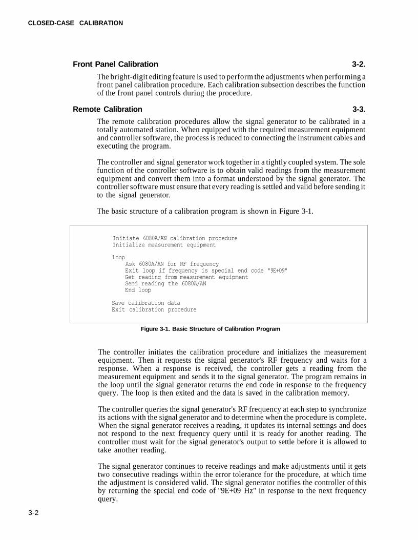
The basic structure of a calibration program is shown in Figure 3-1.
Figure 3-1. Basic Structure of Calibration Program
The controller initiates the calibration procedure and initializes the measurementequipment. Then it requests the signal generator's RF frequency and waits for aresponse. When a response is received, the controller gets a reading from themeasurement equipment and sends it to the signal generator. The program remains inthe loop until the signal generator returns the end code in response to the frequencyquery. The loop is then exited and the data is saved in the calibration memory.
The controller queries the signal generator's RF frequency at each step to synchronizeits actions with the signal generator and to determine when the procedure is complete.When the signal generator receives a reading, it updates its internal settings and doesnot respond to the next frequency query until it is ready for another reading. Thecontroller must wait for the signal generator's output to settle before it is allowed totake another reading.
The signal generator continues to receive readings and make adjustments until it getstwo consecutive readings within the error tolerance for the procedure, at which timethe adjustment is considered valid. The signal generator notifies the controller of thisby returning the special end code of "9E+09 Hz" in response to the next frequencyquery.
3-2
CLOSED-CASE CALIBRATION
The error tolerance is defined for each procedure as a range of readings around thetarget value that the signal generator expects to receive when the adjustment is correct.
The division of responsibility between the controller and signal generator allowsmeasurement equipment from various manufacturers to be used. Adding a differentmeter to the system requires only that a new driver module be written for thecontroller.
NOTE
The design of the controller software has a major impact on the accuracyrealized. One must carefully determine when the readings are settled andaverage several readings before sending the result to the 6080A/AN.Where applicable, the meter specific calibration factors should be appliedto the readings.
A sample program for each of the remote procedures is included in Appendix G. Theprograms are written in Fluke BASIC and run on a Fluke 1722A controller.
Calibration Data 3-4.
The calibration data is stored along with the compensation data in non-volatilememory. A redundant storage scheme enhances the integrity of the data. One copy ofthe data is stored in the battery backed RAM and an identical copy is stored in theEEPROM.
The rear panel slide switch labeled CAL|COMP must be set to the 1 (ON) positionbefore a calibration procedure can be initiated. The CAL and COMP annunciatorsflash when the switch is in the 1 (ON) position. When a calibration procedure isinitiated, the CAL and COMP annunciators stop flashing, and the CAL annunciatorremains lit during the procedure. When the switch is in the 0 (OFF) position, the data iswrite protected in hardware.
The calibration data can be generated in one of two ways: by the Fluke factory or bythe user. Each calibration data segment contains a data origin tag which specifies howthe data was created.
Special function 05 displays the calibration and compensation data origin codes. If nouser calibration or compensation procedures have been performed, the specialfunction displays origin code 00 to signify that all of the data originated at the Flukefactory. If any user calibration procedures have been performed, the correspondingcode is displayed. For example, if the AM calibration procedure has been performedby the user, the data origin special function will display the code 528. A complete list ofthe data origin codes is given in Appendix F.
3-3
CLOSED-CASE CALIBRATION
AM CALIBRATION 3-5.
The AM calibration procedures allow a single point calibration of the AM depth to beperformed. An RF modulation meter is connected to the 6080A/AN's RF output andthe AM calibration factor is adjusted based on the meter reading. The procedurespecific parameters are as follows:
Adjustment Range: ±5% AM DepthAdjustment Resolution: 0.1%Target Value: 50.0%RF Frequency: 300.000000 MHzRF Level: +10.0 dBmInternal AM: ONModulation Frequency: 1 kHzExternal Equipment: RF Modulation Analyzer (HP 8901A or equivalent)
When performing the front panel procedure, use the edit knob to adjust the AM depthuntil the measured AM depth matches the target value. When performing the remoteprocedure, the process is under the control of a program running on an IEEE-488 buscontroller.
The front panel display is reconfigured during the procedures. The target level isdisplayed in the modulation field, the RF frequency is displayed in the frequency field,the adjustment value is displayed in the amplitude field, and the CAL annunciator islit. The display is consistent for the front panel and remote procedures.
All adjustments update a temporary copy of the AM calibration factor. The copy in thecalibration memory is updated only after the store command is given explicitly. Afterthe store command has been given, the internal calibration factor is calculated from thedisplayed adjustment value and is stored in the calibration memory. Subsequent AMprogramming commands use the new calibration factor.
NOTE
Set the rear panel CAL/COMP switch to the 1 (on) position beforeinitiating an AM calibration procedure.
Front Panel AM Calibration Procedure 3-6.
The front panel AM calibration procedure is initiated by the following key sequence:
The display is reconfigured and several of the front panel controls are disabled oroperate differently than they normally do. Table 3-1 shows all of the active controls anddescribes their function while the front panel AM calibration procedure is performed.
Perform the following to execute the front panel AM calibration procedure:
1. Set the rear panel CAL|COMP switch to 1 (on) position.
2. Enter special function 991 to initiate the AM procedure.
3. Connect the 6080A/AN's RF output to the modulation meter.
3-4
CLOSED-CASE CALIBRATION
4. Select the peak+ mode, enable the 50-Hz high-pass filter, and enable the 3 kHzlow-pass filter on the modulation meter.
5. Use the edit knob to change the adjustment value until the modulation meter reads50.0%.
6. Press twice to store the new data.
Table 3-1. Front Panel Controls for AM Calibration Procedure
CONTROLS
KNOB
FUNCTION AND DESCRIPTION
Bright-Digit Editing
Turn the edit knob to adjust the AM calibration factor. Use the left/rightarrow keys to move the bright-digit within the adjustment field. Thebright-digit is always located in the adjustment field.
RF on/off
Toggles the RF output on/off.
Overrange/uncal or Rejected Entry Status
Normally displays the overrange/uncal status. Displays the rejected entrystatus code if there is a rejected entry.
Store Measured Data
Press once; the prompt "Sto ?" is displayed.
Press again to store the data. The message "— Sto —" is displayed toconfirm the selection. The updated calibration factor is stored in thecalibration memory, and the last valid instrument state is restored.
Press any other key to cancel the store operation and resume theprocedure.
Abort the Cal Procedure
Press once; the prompt "Clr ?" is displayed.
Press again to abort the procedure. The message "— Clr —" is displayedto confirm the selection. All measured data is discarded and the previousinstrument state is restored.
Press any other key to resume the procedure.
3-5
CLOSED-CASE CALIBRATION
Remote AM Calibration Procedure 3-7.
This following paragraphs describe the remote AM calibration procedure, the remotecommands used in the procedure, and the elements required to build a functioningcontroller program. Refer to the heading "Remote Calibration" (earlier in Section 3)for general information relating to all remote calibration procedures.
A complete program listing that runs on a Fluke 1722A controller is provided inAppendix G.
The basic structure of the AM calibration program is shown in the program in Figure3-2.
initiate the AM calibration procedure with "CAL_AM"initialize modulation meter
MAIN_LOOP:request the RF frequency with "CC_FREQ?"
if( frequency = 9e9) goto DONE
read modulation metersend reading to 6080A/AN with "CC_RDAM"
goto MAIN_LOOP
DONE:store new data in calibration memory with "CC_SAVE"end
Figure 3-2. Structure of the AM Calibration Program
The procedure is initiated by the command CAL_AM. The controller requests thesignal generator's center frequency with the command CC_FREQ? and waits for aresponse. When a response is received, the controller gets a mod meter reading andsends it to the signal generator with the command CC_RDAM. The program remainsin the main loop until the signal generator returns the end code "9E+09, Hz" inresponse to the CC_FREQ? command. The main loop is then exited and the data issaved with the CC_SAVE command.
Each time the signal generator receives a reading from the controller, it adjusts itsinternal settings and programs the new AM depth. When the signal generator receivestwo consecutive readings within 0.1% of the target value (50.0%), it considers theadjustment value correct and returns the end code.
The controller program must ensure that each mod meter reading is settled beforesending the reading to the 6080A/AN. The program listing in Appendix G uses asimple but effective method to obtain valid mod meter readings.
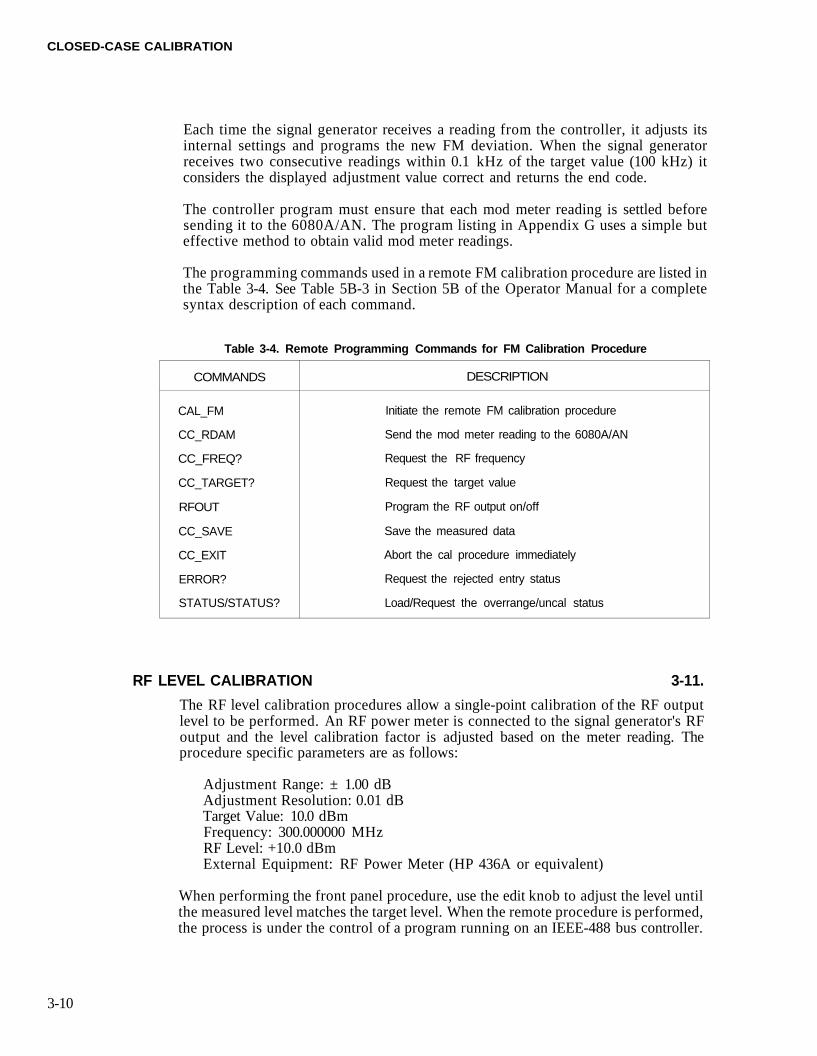
The programming commands used in a remote AM calibration procedure are listed inthe Table 3-2. See Table 5B-3 in Section 5B of the Operator Manual for a completesyntax description of each command.
3-6
CLOSED-CASE CALIBRATION
Table 3-2. Remote Programming Commands for AM Calibration Procedure
COMMANDS
CAL_AM
CC_RDAM
CC_FREQ?
CC_TARGET?
RFOUT
CC_SAVE
CC_EXIT
ERROR?
STATUS/STATUS?
DESCRIPTION
Initiate the remote AM calibration procedure
Send the mod meter reading to the 6080A/AN
Request the RF frequency
Request the target value
Program the RF output on/off
Save the measured data
Abort the cal procedure immediately
Request the rejected entry status
Load/Request the overrange/uncal status
FM CALIBRATION 3-8.
The FM calibration procedures allow a single point calibration of the FM deviation tobe performed. An RF modulation meter is connected to the 6080A/AN's RF output,and the FM calibration factor is adjusted based on the meter reading. The procedurespecific parameters are as follows:
Adjustment Range: ± 10 kHzAdjustment Resolution: 0.1 kHzTarget Value: 100 kHzFrequency: 640.000000 MHzRF Level: +10.0 dBmInternal AM: ONModulation Frequency: 1 kHzExternal Equipment: RF Modulation Analyzer (HP 8901A or equivalent)
When performing the front panel procedure, use the edit knob to adjust the FMdeviation until the measured FM deviation matches the target value. When the remoteprocedure is performed, the process is under the control of a program running on anIEEE-488 bus controller.
The front panel display is reconfigured during the procedures. The target level isdisplayed in the modulation field, the RF frequency is displayed in the frequency field,the adjustment value is displayed in the amplitude field, and the CAL annunciator islit. The display is consistent for the front panel and remote procedures.
All adjustments update a temporary copy of the FM calibration factor. The copy in thecalibration memory is updated only after the store command is given explicitly. Afterthe store command has been given, the internal calibration factor is calculated from thedisplayed adjustment value and is stored in the calibration memory. Subsequent FMprogramming commands use the new calibration factor.
NOTE
Set the rear panel CAL COMP switch to the 1 (on) position beforeinitiating an FM calibration procedure.
3-7
CLOSED-CASE CALIBRATION
Front Panel FM Calibration Procedure 3-9.
The front panel FM calibration procedure is initiated by the following key sequence:
The display is reconfigured for the procedure. Several of the front panel controls aredisabled or operate differently than they normally do. Table 3-3. shows all of the activecontrols and describes their function while performing the front panel FM calibrationprocedure.
Table 3-3. Front Panel Controls for FM Calibration Procedure
CONTROLS
KNOB
FUNCTION AND DESCRIPTION
Bright-Digit Editing
Turn the edit knob to adjust the FM calibration factor. Use the left/rightarrow keys to move the bright-digit within the adjustment field. Thebright-digit is always located in the adjustment field.
RF on/off
Toggles the RF output on/off.
Overrange/uncal or Rejected Entry Status
Normally displays the overrange/uncal status. Displays the rejected entrystatus code if there is a rejected entry.
Store Measured Data
Press once; the prompt "Sto ?" is displayed.
Press again to store the data. The message "— Sto —" is displayed toconfirm the selection. The updated calibration factor is stored in thecalibration memory, and the last valid instrument state is restored.
Press any other key to cancel the store operation and resume theprocedure.
Abort the Cal Procedure
Press once; the prompt "Clr ?" is displayed.
Press again to abort the procedure. The message "— Clr —" is displayedto confirm the selection. All measured data is discarded and the previousinstrument state is restored.
Press any other key to resume the procedure.
3-8
CLOSED-CASE CALIBRATION
Perform the following to execute the front panel FM calibration procedure:
1. Set the rear panel CAL|COMP switch to the 1 (on) position.
2. Enter special function 992 to initiate the FM procedure.
3. Connect the 6080A/AN's RF output to the modulation meter.
4. Select the peak+ mode, enable the 50-Hz high-pass filter, and enable the 3 kHzlow-pass filter on the modulation meter.
5. Use the edit knob to change the adjustment value until the modulation meter reads100 kHz
6. Press the key twice to store the new data.
Remote FM Calibration 3-10.
The following paragraphs describe the remote FM calibration procedure, the remotecommands used in the procedure, and the elements required to build a functioningcontroller program. Refer to the heading "Remote Calibration" (earlier in Section 3)for general information relating to all remote calibration procedures.
A complete program listing that runs on a Fluke 1722A controller is provided inAppendix G.
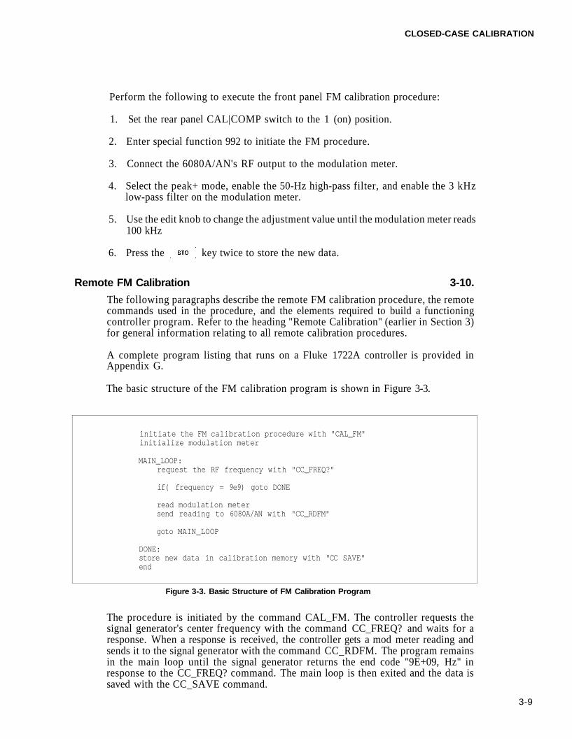
The basic structure of the FM calibration program is shown in Figure 3-3.
initiate the FM calibration procedure with "CAL_FM"initialize modulation meter
MAIN_LOOP:request the RF frequency with "CC_FREQ?"
if( frequency = 9e9) goto DONE
read modulation metersend reading to 6080A/AN with "CC_RDFM"
goto MAIN_LOOP
DONE:store new data in calibration memory with "CC SAVE"end
Figure 3-3. Basic Structure of FM Calibration Program
The procedure is initiated by the command CAL_FM. The controller requests thesignal generator's center frequency with the command CC_FREQ? and waits for aresponse. When a response is received, the controller gets a mod meter reading andsends it to the signal generator with the command CC_RDFM. The program remainsin the main loop until the signal generator returns the end code "9E+09, Hz" inresponse to the CC_FREQ? command. The main loop is then exited and the data issaved with the CC_SAVE command.
3-9
CLOSED-CASE CALIBRATION
Each time the signal generator receives a reading from the controller, it adjusts itsinternal settings and programs the new FM deviation. When the signal generatorreceives two consecutive readings within 0.1 kHz of the target value (100 kHz) itconsiders the displayed adjustment value correct and returns the end code.
The controller program must ensure that each mod meter reading is settled beforesending it to the 6080A/AN. The program listing in Appendix G uses a simple buteffective method to obtain valid mod meter readings.
The programming commands used in a remote FM calibration procedure are listed inthe Table 3-4. See Table 5B-3 in Section 5B of the Operator Manual for a completesyntax description of each command.
Table 3-4. Remote Programming Commands for FM Calibration Procedure
COMMANDS
CAL_FM
CC_RDAM
CC_FREQ?
CC_TARGET?
RFOUT
CC_SAVE
CC_EXIT
ERROR?
STATUS/STATUS?
DESCRIPTION
Initiate the remote FM calibration procedure
Send the mod meter reading to the 6080A/AN
Request the RF frequency
Request the target value
Program the RF output on/off
Save the measured data
Abort the cal procedure immediately
Request the rejected entry status
Load/Request the overrange/uncal status
RF LEVEL CALIBRATION 3-11.
The RF level calibration procedures allow a single-point calibration of the RF outputlevel to be performed. An RF power meter is connected to the signal generator's RFoutput and the level calibration factor is adjusted based on the meter reading. Theprocedure specific parameters are as follows:
Adjustment Range: ± 1.00 dBAdjustment Resolution: 0.01 dBTarget Value: 10.0 dBmFrequency: 300.000000 MHzRF Level: +10.0 dBmExternal Equipment: RF Power Meter (HP 436A or equivalent)
When performing the front panel procedure, use the edit knob to adjust the level untilthe measured level matches the target level. When the remote procedure is performed,the process is under the control of a program running on an IEEE-488 bus controller.
3-10
CLOSED-CASE CALIBRATION
The front panel display is reconfigured during the procedures. The target level isdisplayed in the modulation field, the RF frequency is displayed in the frequency field,the adjustment value is displayed in the amplitude field, and the CAL annunciator islit. The display is consistent for the front panel and remote procedures.
All adjustments update a temporary copy of the adjustment value. The copy in thecalibration memory is updated only after the store command is given explicitly. Afterthe store command has been given, the internal calibration factor is calculated from thedisplayed adjustment value and is stored in the calibration memory. Subsequentamplitude programming commands use the new calibration factor.
NOTE
Set the rear panel CAL/COMP switch to the 1 (on) position beforeinitiating the calibration procedures.
Front Panel Level Calibration Procedure 3-12.
The front panel level calibration procedure is initiated by the following key sequence:
The display is reconfigured for the procedure. Several of the front panel controls aredisabled or operate differently than they normally do. Table 3-5. shows all of the activecontrols and describes their function while performing the front panel level calibrationprocedure.
Perform the following to execute the front panel level calibration procedure:
1. Set the rear panel CAL|COMP switch to the 1 (on) position.
2. Enter special function 993 to initiate the procedure.
3. Connect the signal generator's RF output to the power meter.
4. Set the appropriate power meter calibration factor (if required) and zero the powermeter.
5. Use the edit knob to change the adjustment value until the power meter reads +10dBm.
6. Press the key twice to store the new data.
3-11
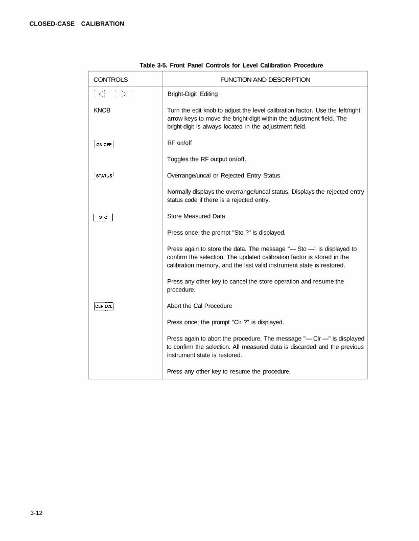
CLOSED-CASE CALIBRATION
Table 3-5. Front Panel Controls for Level Calibration Procedure
3-12
CONTROLS
KNOB
FUNCTION AND DESCRIPTION
Bright-Digit Editing
Turn the edit knob to adjust the level calibration factor. Use the left/rightarrow keys to move the bright-digit within the adjustment field. Thebright-digit is always located in the adjustment field.
RF on/off
Toggles the RF output on/off.
Overrange/uncal or Rejected Entry Status
Normally displays the overrange/uncal status. Displays the rejected entrystatus code if there is a rejected entry.
Store Measured Data
Press once; the prompt "Sto ?" is displayed.
Press again to store the data. The message "— Sto —" is displayed toconfirm the selection. The updated calibration factor is stored in thecalibration memory, and the last valid instrument state is restored.
Press any other key to cancel the store operation and resume theprocedure.
Abort the Cal Procedure
Press once; the prompt "Clr ?" is displayed.
Press again to abort the procedure. The message "— Clr —" is displayedto confirm the selection. All measured data is discarded and the previousinstrument state is restored.
Press any other key to resume the procedure.
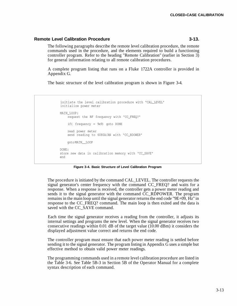
CLOSED-CASE CALIBRATION
Remote Level Calibration Procedure 3-13.
The following paragraphs describe the remote level calibration procedure, the remotecommands used in the procedure, and the elements required to build a functioningcontroller program. Refer to the heading "Remote Calibration" (earlier in Section 3)for general information relating to all remote calibration procedures.
A complete program listing that runs on a Fluke 1722A controller is provided inAppendix G.
The basic structure of the level calibration program is shown in Figure 3-4.
initiate the level calibration procedure with "CAL_LEVEL"initialize power meter
MAIN_LOOP:request the RF frequency with "CC_FREQ?"
if( frequency = 9e9) goto DONE
read power metersend reading to 6080A/AN with "CC_RDOWER"
goto MAIN__LOOP
DONE:store new data in calibration memory with "CC_SAVE"end
Figure 3-4. Basic Structure of Level Calibration Program
The procedure is initiated by the command CAL_LEVEL. The controller requests thesignal generator's center frequency with the command CC_FREQ? and waits for aresponse. When a response is received, the controller gets a power meter reading andsends it to the signal generator with the command CC_RDPOWER. The programremains in the main loop until the signal generator returns the end code "9E+09, Hz" inresponse to the CC_FREQ? command. The main loop is then exited and the data issaved with the CC_SAVE command.
Each time the signal generator receives a reading from the controller, it adjusts itsinternal settings and programs the new level. When the signal generator receives twoconsecutive readings within 0.01 dB of the target value (10.00 dBm) it considers thedisplayed adjustment value correct and returns the end code.
The controller program must ensure that each power meter reading is settled beforesending it to the signal generator. The program listing in Appendix G uses a simple buteffective method to obtain valid power meter readings.
The programming commands used in a remote level calibration procedure are listed inthe Table 3-6. See Table 5B-3 in Section 5B of the Operator Manual for a completesyntax description of each command.
3-13
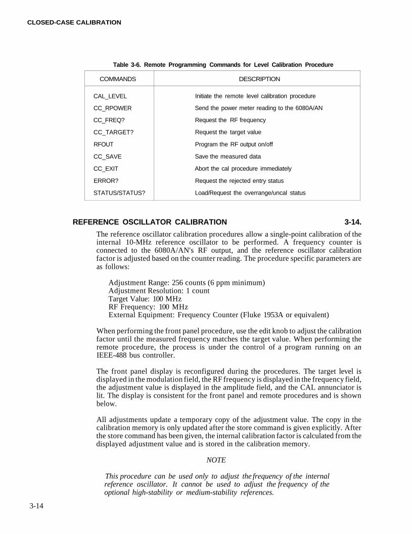
CLOSED-CASE CALIBRATION
Table 3-6. Remote Programming Commands for Level Calibration Procedure
COMMANDS
CAL_LEVEL
CC_RPOWER
CC_FREQ?
CC_TARGET?
RFOUT
CC_SAVE
CC_EXIT
ERROR?
STATUS/STATUS?
DESCRIPTION
Initiate the remote level calibration procedure
Send the power meter reading to the 6080A/AN
Request the RF frequency
Request the target value
Program the RF output on/off
Save the measured data
Abort the cal procedure immediately
Request the rejected entry status
Load/Request the overrange/uncal status
REFERENCE OSCILLATOR CALIBRATION 3-14.
The reference oscillator calibration procedures allow a single-point calibration of theinternal 10-MHz reference oscillator to be performed. A frequency counter isconnected to the 6080A/AN's RF output, and the reference oscillator calibrationfactor is adjusted based on the counter reading. The procedure specific parameters areas follows:
Adjustment Range: 256 counts (6 ppm minimum)Adjustment Resolution: 1 countTarget Value: 100 MHzRF Frequency: 100 MHzExternal Equipment: Frequency Counter (Fluke 1953A or equivalent)
When performing the front panel procedure, use the edit knob to adjust the calibrationfactor until the measured frequency matches the target value. When performing theremote procedure, the process is under the control of a program running on anIEEE-488 bus controller.
The front panel display is reconfigured during the procedures. The target level isdisplayed in the modulation field, the RF frequency is displayed in the frequency field,the adjustment value is displayed in the amplitude field, and the CAL annunciator islit. The display is consistent for the front panel and remote procedures and is shownbelow.
All adjustments update a temporary copy of the adjustment value. The copy in thecalibration memory is only updated after the store command is given explicitly. Afterthe store command has been given, the internal calibration factor is calculated from thedisplayed adjustment value and is stored in the calibration memory.
NOTE
This procedure can be used only to adjust the frequency of the internalreference oscillator. It cannot be used to adjust the frequency of theoptional high-stability or medium-stability references.
3-14
CLOSED-CASE CALIBRATION
NOTE
The rear panel CAL|COMP switch must be set to the 1 (on) positionbefore initiating the calibration procedures.
Front Panel Reference Oscillator Calibration Procedure 3-15.
The front panel reference oscillator calibration procedure is initiated by the followingkey sequence:
The display is reconfigured for the procedure. Several of the front panel controls aredisabled or operate differently than they normally do. Table 3-7. shows all of the activecontrols and describes their function while performing the procedure.
Table 3-7. Front Panel Controls for Reference Oscillator Calibration Procedure
CONTROLS
KNOB
FUNCTION AND DESCRIPTION
Bright-Digit Editing
Turn the edit knob to adjust the reference oscillator calibration factor.Use the left/right arrow keys to move the bright-digit within the adjust-ment field. The bright-digit is always located in the adjustment field.
RF on/off
Toggles the RF output on/off.
Overrange/uncal or Rejected Entry Status
Normally displays the overrange/uncal status. Displays the rejected entrystatus code if there is a rejected entry.
Store Measured Data
Press once; the prompt "Sto ?" is displayed.
Press again to store the data. The message "— Sto —" is displayed toconfirm the selection. The updated calibration factor is stored in thecalibration memory, and the last valid instrument state is restored.
Press any other key to cancel the store operation and resume theprocedure.
Abort the Cal Procedure
Press once; the prompt "Clr ?" is displayed.
Press again to abort the procedure. The message "— Clr —" is displayedto confirm the selection. All measured data is discarded and the previousinstrument state is restored.
Press any other key to resume the procedure.
3-15
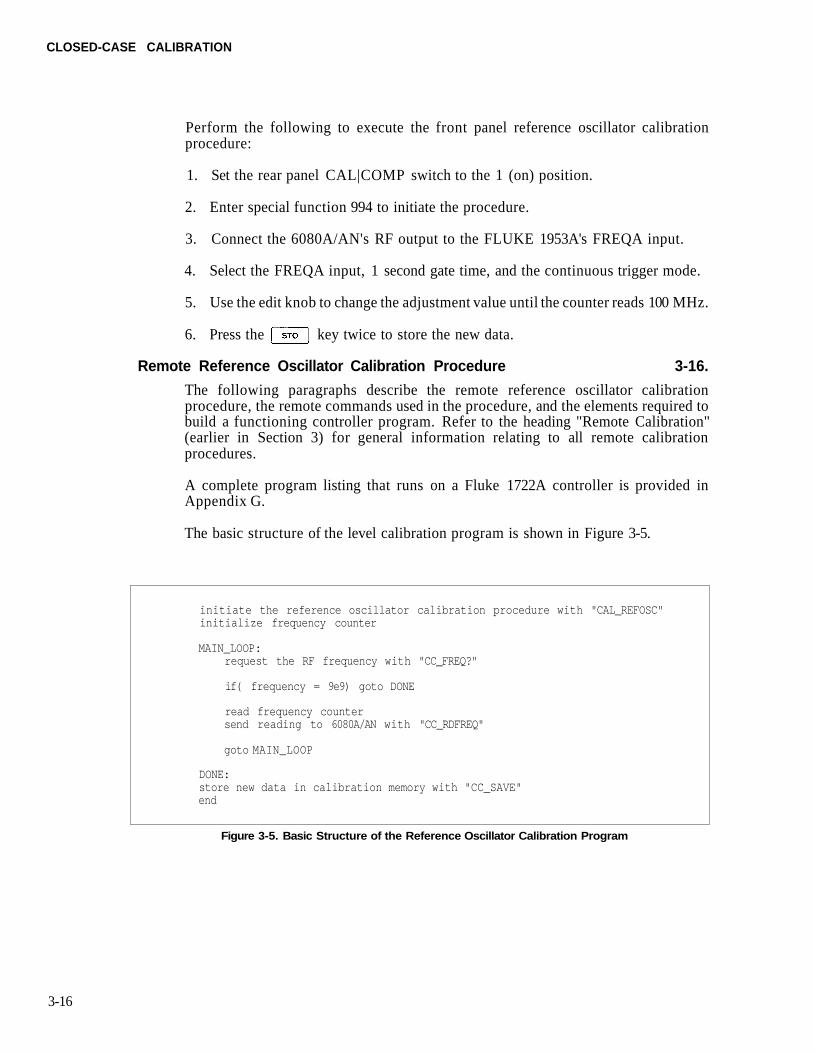
CLOSED-CASE CALIBRATION
Perform the following to execute the front panel reference oscillator calibrationprocedure:
1. Set the rear panel CAL|COMP switch to the 1 (on) position.
2. Enter special function 994 to initiate the procedure.
3. Connect the 6080A/AN's RF output to the FLUKE 1953A's FREQA input.
4. Select the FREQA input, 1 second gate time, and the continuous trigger mode.
5. Use the edit knob to change the adjustment value until the counter reads 100 MHz.
6. Press the key twice to store the new data.
Remote Reference Oscillator Calibration Procedure 3-16.
The following paragraphs describe the remote reference oscillator calibrationprocedure, the remote commands used in the procedure, and the elements required tobuild a functioning controller program. Refer to the heading "Remote Calibration"(earlier in Section 3) for general information relating to all remote calibrationprocedures.
A complete program listing that runs on a Fluke 1722A controller is provided inAppendix G.
The basic structure of the level calibration program is shown in Figure 3-5.
initiate the reference oscillator calibration procedure with "CAL_REFOSC"initialize frequency counter
MAIN_LOOP:request the RF frequency with "CC_FREQ?"
if( frequency = 9e9) goto DONE
read frequency countersend reading to 6080A/AN with "CC_RDFREQ"
goto MAIN_LOOP
DONE:store new data in calibration memory with "CC_SAVE"end
Figure 3-5. Basic Structure of the Reference Oscillator Calibration Program
3-16
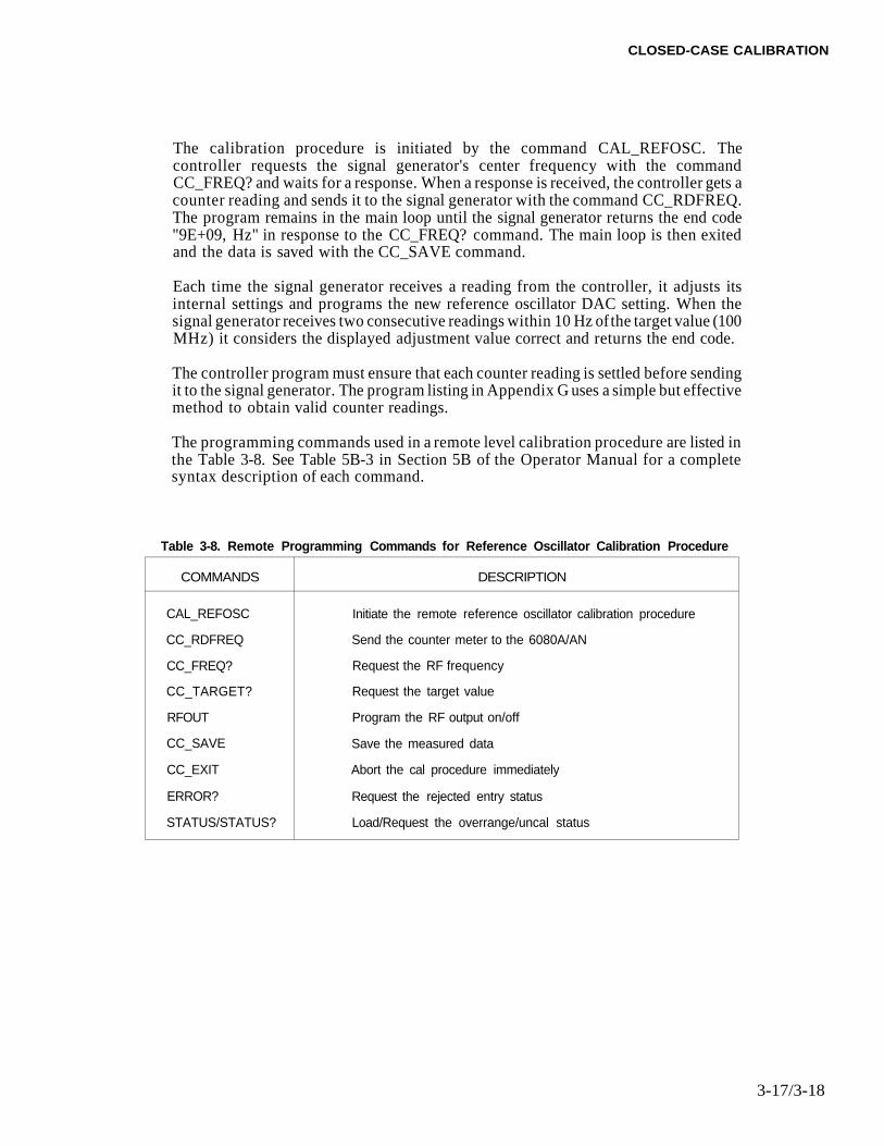
CLOSED-CASE CALIBRATION
The calibration procedure is initiated by the command CAL_REFOSC. Thecontroller requests the signal generator's center frequency with the commandCC_FREQ? and waits for a response. When a response is received, the controller gets acounter reading and sends it to the signal generator with the command CC_RDFREQ.The program remains in the main loop until the signal generator returns the end code"9E+09, Hz" in response to the CC_FREQ? command. The main loop is then exitedand the data is saved with the CC_SAVE command.
Each time the signal generator receives a reading from the controller, it adjusts itsinternal settings and programs the new reference oscillator DAC setting. When thesignal generator receives two consecutive readings within 10 Hz of the target value (100MHz) it considers the displayed adjustment value correct and returns the end code.
The controller program must ensure that each counter reading is settled before sendingit to the signal generator. The program listing in Appendix G uses a simple but effectivemethod to obtain valid counter readings.
The programming commands used in a remote level calibration procedure are listed inthe Table 3-8. See Table 5B-3 in Section 5B of the Operator Manual for a completesyntax description of each command.
Table 3-8. Remote Programming Commands for Reference Oscillator Calibration Procedure
COMMANDS
CAL_REFOSC
CC_RDFREQ
CC_FREQ?
CC_TARGET?
RFOUT
CC_SAVE
CC_EXIT
ERROR?
STATUS/STATUS?
DESCRIPTION
Initiate the remote reference oscillator calibration procedure
Send the counter meter to the 6080A/AN
Request the RF frequency
Request the target value
Program the RF output on/off
Save the measured data
Abort the cal procedure immediately
Request the rejected entry status
Load/Request the overrange/uncal status
3-17/3-18

Section 4Performance Tests
INTRODUCTION 4-1.
The information in the Section 4 describes the performance tests for the keyparameters of the 6080A/AN Synthesized Signal Generator (also referred tothroughout as the "signal generator").
Instrument specifications are used as the performance standard. These closed-caseperformance tests may be used as:
• An acceptance test upon receipt of the instrument
• An indication that repair and/or calibration is required
• A performance verification after completing repairs or calibration of theinstrument.
Individual performance tests can also be used as troubleshooting aids.
The signal generator being tested (referred to as UUT — the "unit under test") must bewarmed up with all covers in place for at least 2 hours before starting the performancetests.
Fluke recommends that calibration be performed once a year.
TEST EQUIPMENT 4-2.
Table 4-1 lists the recommended test equipment for the performance tests, adjustmentprocedures, and troubleshooting the signal generator. Figure 4-1 shows a two-turnloop.
4-1
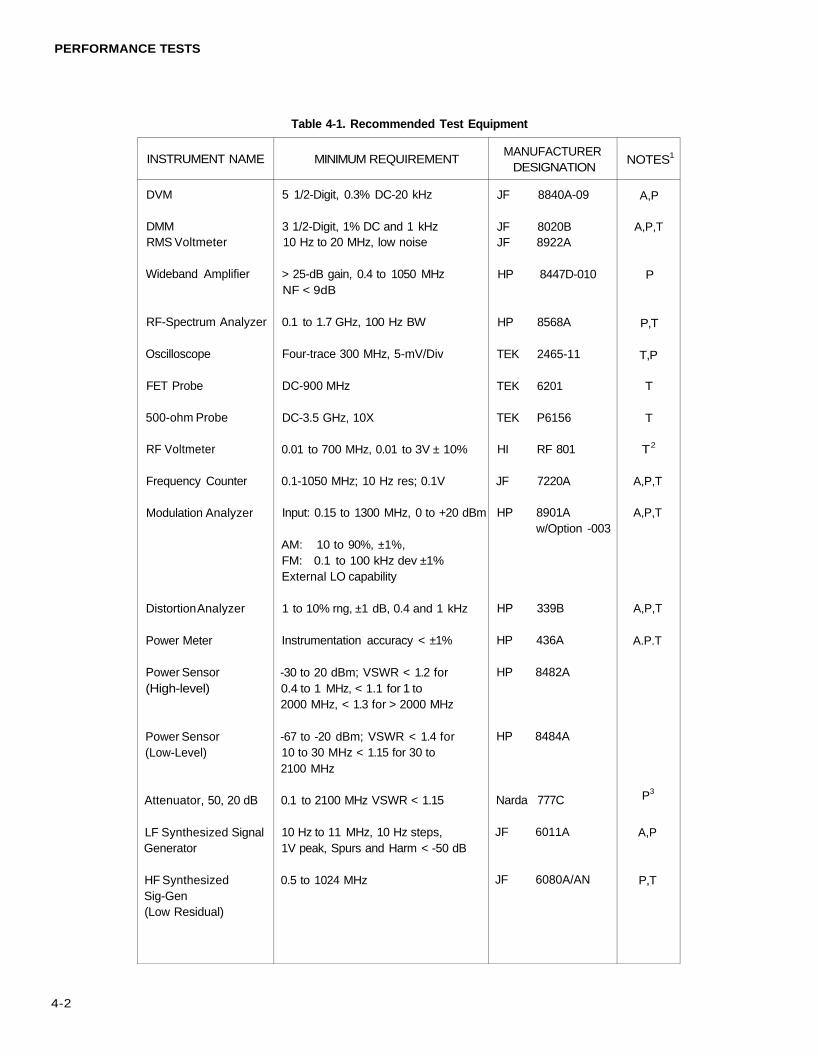
PERFORMANCE TESTS
Table 4-1. Recommended Test Equipment
INSTRUMENT NAME
DVM
DMMRMS Voltmeter
Wideband Amplifier
RF-Spectrum Analyzer
Oscilloscope
FET Probe
500-ohm Probe
RF Voltmeter
Frequency Counter
Modulation Analyzer
Distortion Analyzer
Power Meter
Power Sensor(High-level)
Power Sensor(Low-Level)
Attenuator, 50, 20 dB
LF Synthesized SignalGenerator
HF SynthesizedSig-Gen(Low Residual)
MINIMUM REQUIREMENT
5 1/2-Digit, 0.3% DC-20 kHz
3 1/2-Digit, 1% DC and 1 kHz10 Hz to 20 MHz, low noise
> 25-dB gain, 0.4 to 1050 MHzNF < 9dB
0.1 to 1.7 GHz, 100 Hz BW
Four-trace 300 MHz, 5-mV/Div
DC-900 MHz
DC-3.5 GHz, 10X
0.01 to 700 MHz, 0.01 to 3V ± 10%
0.1-1050 MHz; 10 Hz res; 0.1V
Input: 0.15 to 1300 MHz, 0 to +20 dBm
AM: 10 to 90%, ±1%,FM: 0.1 to 100 kHz dev ±1%External LO capability
1 to 10% rng, ±1 dB, 0.4 and 1 kHz
Instrumentation accuracy < ±1%
-30 to 20 dBm; VSWR < 1.2 for0.4 to 1 MHz, < 1.1 for 1 to2000 MHz, < 1.3 for > 2000 MHz
-67 to -20 dBm; VSWR < 1.4 for10 to 30 MHz < 1.15 for 30 to2100 MHz
0.1 to 2100 MHz VSWR < 1.15
10 Hz to 11 MHz, 10 Hz steps,1V peak, Spurs and Harm < -50 dB
0.5 to 1024 MHz
MANUFACTURERDESIGNATION
JF 8840A-09
JF 8020BJF 8922A
HP 8447D-010
HP 8568A
TEK 2465-11
TEK 6201
TEK P6156
HI RF 801
JF 7220A
HP 8901Aw/Option -003
HP 339B
HP 436A
HP 8482A
HP 8484A
Narda 777C
JF 6011A
JF 6080A/AN
NOTES1
A,P
A,P,T
P
P,T
T,P
T
T
T2
A,P,T
A,P,T
A,P,T
A.P.T
P3
A,P
P,T
4-2
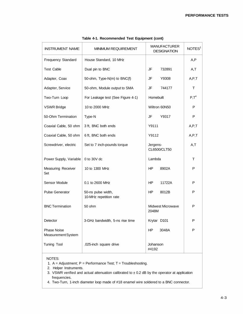
PERFORMANCE TESTS
Table 4-1. Recommended Test Equipment (cont)
INSTRUMENT NAME
Frequency Standard
Test Cable
Adapter, Coax
Adapter, Service
Two-Turn Loop
VSWR Bridge
50-Ohm Termination
Coaxial Cable, 50 ohm
Coaxial Cable, 50 ohm
Screwdriver, electric
Power Supply, Variable
Measuring ReceiverSet
Sensor Module
Pulse Generator
BNC Termination
Detector
Phase NoiseMeasurement System
Tuning Tool
MINIMUM REQUIREMENT
House Standard, 10 MHz
Dual pin to BNC
50-ohm, Type-N(m) to BNC(f)
50-ohm, Module output to SMA
For Leakage test (See Figure 4-1)
10 to 2000 MHz
Type-N
3 ft, BNC both ends
6 ft, BNC both ends
Set to 7 inch-pounds torque
0 to 30V dc
10 to 1300 MHz
0.1 to 2600 MHz
50-ns pulse width,10-MHz repetition rate
50 ohm
3-GHz bandwidth, 5-ns rise time
.025-inch square drive
MANUFACTURERDESIGNATION
JF 732891
JF Y9308
JF 744177
Homebuilt
Wiltron 60N50
JF Y9317
Y9111
Y9112
Jergens-CL6500/CLT50
Lambda
HP 8902A
HP 11722A
HP 8012B
Midwest Microwave2048M
Krytar D101
HP 3048A
Johanson#4192
NOTES1
A,P
A,T
A,P,T
T
P,T4
P
P
A,P,T
A,P,T
A,T
T
P
P
P
P
P
P
NOTES:1. A = Adjustment; P = Performance Test; T = Troubleshooting.2. Helper Instruments.3. VSWR verified and actual attenuation calibrated to ± 0.2 dB by the operator at application
frequencies.4. Two-Turn, 1-inch diameter loop made of #18 enamel wire soldered to a BNC connector.
4-3
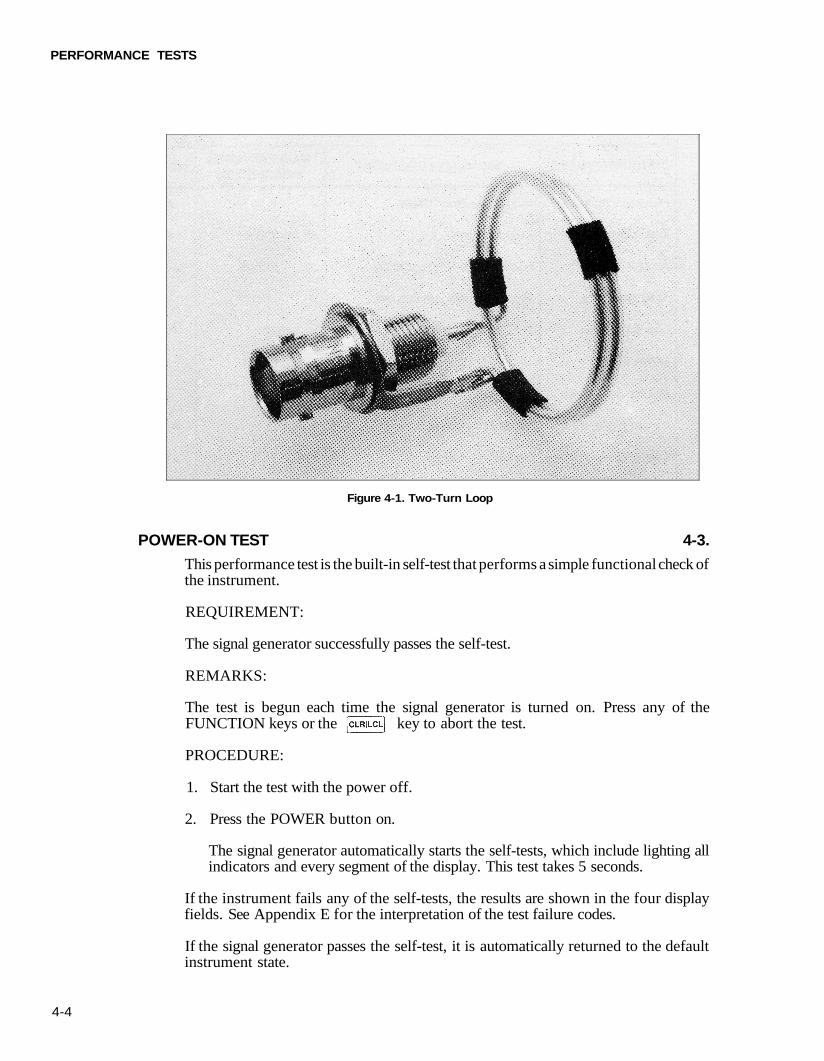
PERFORMANCE TESTS
POWER-ON TEST 4-3.
This performance test is the built-in self-test that performs a simple functional check ofthe instrument.
REQUIREMENT:
The signal generator successfully passes the self-test.
REMARKS:
The test is begun each time the signal generator is turned on. Press any of theFUNCTION keys or the key to abort the test.
PROCEDURE:
1. Start the test with the power off.
2. Press the POWER button on.
The signal generator automatically starts the self-tests, which include lighting allindicators and every segment of the display. This test takes 5 seconds.
If the instrument fails any of the self-tests, the results are shown in the four displayfields. See Appendix E for the interpretation of the test failure codes.
If the signal generator passes the self-test, it is automatically returned to the defaultinstrument state.
4-4
Figure 4-1. Two-Turn Loop
PERFORMANCE TESTS
FREQUENCY ACCURACY TEST 4-4.
The internal time base is compared to that of a Frequency Standard.
REQUIREMENTS:
The frequency of the UUT time base is within the specified limits.
TEST EQUIPMENT:
• Frequency standard• Frequency counter
PROCEDURE:
1. Connect the frequency standard output to the 10 MHZ REF IN connector on thefrequency counter and switch the counter to EXT REF.
2. Switch the UUT to internal reference.
3. Connect the UUT REF OUT connector to the frequency counter CHANNEL Ainput connector.
4. Verify that the counter display is 10 MHz ±100 Hz.
5. Monitor the frequency for one hour to verify its stability within ±0.5 Hz.(Operating temperature within ±5°C).
SYNTHESIS TEST 4-5.
The signal generator output frequency is measured at several programmed frequenciesusing a frequency counter operating on a common reference with the signal generator.
REQUIREMENT:
The signal generator's measured and programmed frequencies agree within ±1 count.
TEST EQUIPMENT:
• Frequency counter
REMARKS:
If the UUT fails this test, the frequency synthesis circuitry is probably at fault. SeeSection 6C.
PROCEDURE:
1. Connect the UUT 10 MHz OUT to the frequency counter 10-MHz reference input,and connect the UUT RF OUTPUT to the frequency counter input.
2. Set the UUT REF INT/EXT switch to INT.
3. Program the UUT to SPCL 909.
4-5
PERFORMANCE TESTS
4. Program the UUT frequency to 111.111111 MHz.
5. Program the UUT frequency step to 111.111111 MHz.
6. Verify that the reading on the frequency counter agrees with the UUT frequency ± 1count as the frequency is stepped from 111.111111 to 999.999999 MHz.
HIGH-LEVEL ACCURACY TEST 4-6.
The output power is measured using a power meter at various frequencies. First thestep attenuator is set for zero attenuation; then each attenuator section is individuallyprogrammed. Finally, the output level accuracy and attenuator section errors arecomputed.
If a measuring receiver is available for level testing, proceed directly to the"ALTERNATE-LEVEL ACCURACY TEST" procedure later in Section 4.
TEST EQUIPMENT:
• Power meter• Power sensor (high-Level)
REQUIREMENT:
The output level accuracy, the attenuator section errors, and the sum of the attenuatorsection errors at each test frequency are:
< ±1.5 dB from 0.5 to 1024 MHz
REMARKS:
If the UUT fails this performance test, it needs to be calibrated (Section 3) or repaired(Section 6). Possible problem areas (if no power-on status codes are present) includethe A8 Output PCA, the A21 Attenuator PCA, or the A7 Relay Driver PCA.
The test frequencies of this procedure provide reasonable confidence of the amplitudeaccuracy of the UUT. However, additional test frequencies may be included in this test.
This test verifies the high-level accuracy of the signal generator and verifies that theamplitude correction factors for the individual attenuator sections are correct. Thistest, in conjunction with the mid-level accuracy and low-level accuracy tests, verifiesthe overall level performance of the UUT.
NOTE
To test attenuator sections 4 through 7, program the 6080A/AN SignalGenerator to -12 dBm, and key in
through , respectively.
PROCEDURE:
1. Calibrate and zero the power meter.
4-6
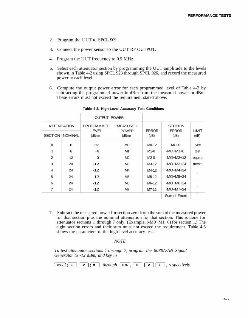
PERFORMANCE TESTS
2. Program the UUT to SPCL 909.
3. Connect the power sensor to the UUT RF OUTPUT.
4. Program the UUT frequency to 0.5 MHz.
5. Select each attenuator section by programming the UUT amplitude to the levelsshown in Table 4-2 using SPCL 923 through SPCL 926, and record the measuredpower at each level.
6. Compute the output power error for each programmed level of Table 4-2 bysubtracting the programmed power in dBm from the measured power in dBm.These errors must not exceed the requirement stated above.
Table 4-2. High-Level Accuracy Test Conditions
ATTENUATION
SECTION
0
1
2
3
4
5
6
7
NOMINAL
0
6
12
24
24
24
24
24
OUTPUT POWER
PROGRAMMEDLEVEL(dBm)
+12
+6
0
-12
-12
-12
-12
-12
MEASUREDPOWER(dBm)
MO
M1
M2
M3
M4
M5
M6
M7
ERROR(dB)
M0-12
M1-6
M2-0
M3-12
M4-12
M5-12
M6-12
M7-12
SECTIONERROR
(dB)
MO-12
-MO+M1+6
-MO+M2+12
-MO+M3+24
-MO+M4+24
-MO+M5+24
-MO+M6+24
-MO+M7+24
Sum of Errors
LIMIT(dB)
See
test
require-
ments"
"
"
"
"
7. Subtract the measured power for section zero from the sum of the measured powerfor that section plus the nominal attenuation for that section. This is done forattenuator sections 1 through 7 only. (Example, (-M0+M1+6) for section 1.) Theeight section errors and their sum must not exceed the requirement. Table 4-3shows the parameters of the high-level accuracy test.
NOTE
To test attenuator sections 4 through 7, program the 6080A/AN SignalGenerator to -12 dBm, and key in
through , respectively.
4-7
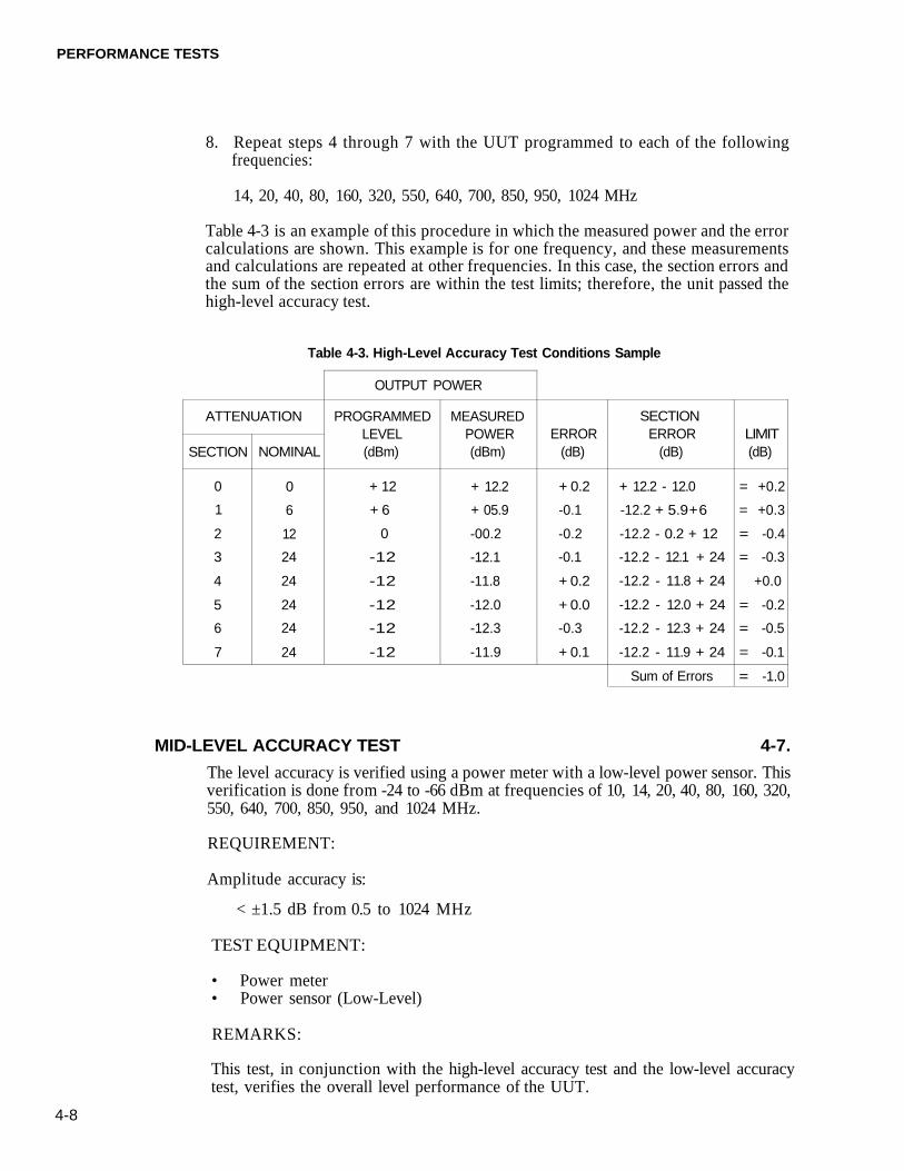
PERFORMANCE TESTS
8. Repeat steps 4 through 7 with the UUT programmed to each of the followingfrequencies:
14, 20, 40, 80, 160, 320, 550, 640, 700, 850, 950, 1024 MHz
Table 4-3 is an example of this procedure in which the measured power and the errorcalculations are shown. This example is for one frequency, and these measurementsand calculations are repeated at other frequencies. In this case, the section errors andthe sum of the section errors are within the test limits; therefore, the unit passed thehigh-level accuracy test.
Table 4-3. High-Level Accuracy Test Conditions Sample
ATTENUATION
SECTION
0
1
2
3
4
5
6
7
NOMINAL
0
6
12
24
24
24
24
24
OUTPUT POWER
PROGRAMMEDLEVEL(dBm)
+ 12
+ 6
0
-12
-12
-12
-12
-12
MEASUREDPOWER(dBm)
+ 12.2
+ 05.9
-00.2
-12.1
-11.8
-12.0
-12.3
-11.9
ERROR(dB)
+ 0.2
-0.1
-0.2
-0.1
+ 0.2
+ 0.0
-0.3
+ 0.1
SECTIONERROR
(dB)
+ 12.2 - 12.0
-12.2 + 5.9 + 6
-12.2 - 0.2 + 12
-12.2 - 12.1 + 24
-12.2 - 11.8 + 24
-12.2 - 12.0 + 24
-12.2 - 12.3 + 24
-12.2 - 11.9 + 24
Sum of Errors
LIMIT(dB)
= +0.2
= +0.3
= -0.4
= -0.3
+0.0
= -0.2
= -0.5
= -0.1
= -1.0
MID-LEVEL ACCURACY TEST 4-7.
The level accuracy is verified using a power meter with a low-level power sensor. Thisverification is done from -24 to -66 dBm at frequencies of 10, 14, 20, 40, 80, 160, 320,550, 640, 700, 850, 950, and 1024 MHz.
REQUIREMENT:
Amplitude accuracy is:
< ±1.5 dB from 0.5 to 1024 MHz
TEST EQUIPMENT:
• Power meter• Power sensor (Low-Level)
REMARKS:
This test, in conjunction with the high-level accuracy test and the low-level accuracytest, verifies the overall level performance of the UUT.
4-8
PERFORMANCE TESTS
If the UUT fails this test after passing the high level accuracy test, problems with theA21 Attenuator PCA or the A7 Relay Driver PCA are indicated.
It is convenient to use the UUT RF ON/OFF control when zeroing the power meter.
PROCEDURE:
1. Program the UUT to SPCL 909, 10 MHz, and -24 dBm.
2. Calibrate the power meter.
3. Zero the power meter.
4. Connect the power meter and power sensor to the UUT RF OUTPUT.
5. Measure the UUT output power (in dBm) with the power meter. The outputshould agree with the programmed level within the requirement.
6. Repeat step 5 for levels of -30, -36, -42, -48, -54, -60, and -66 dBm.
7. Repeat steps 5 and 6 for frequencies of 14, 20, 40, 80, 160, 320, 550, 640, 700, 850,950, and 1024 MHz.
LOW-LEVEL ACCURACY TEST 4-8.
An RF spectrum analyzer and amplifier are used to verify the UUT level accuracy at-137 dBm and at frequencies of 10, 14, 20, 40, 80, 160, 320, 550, 640, 700, 850, 950, and1024 MHz.
REQUIREMENT:
Amplitude accuracy is:
< ±1.5 dB from 0.5 to 1024 MHz for level between -66 dBm and -117 dBm.< ±3.0 dB from 0.5 to 1024 MHz for level between -117 dBm and -137 dBm.
TEST EQUIPMENT:
0.1 - to 1.1-GHz amplifier50-dB attenuator20-dB attenuatorRF spectrum analyzerPower meterPower sensor (low-level)
REMARKS:
This test, in conjunction with the mid-level accuracy and high-Level accuracy test,verifies the overall level performance of the UUT.
If the UUT fails this test after passing the "High-Level Accuracy Test and the"Mid-Level Accuracy Test" a problem in the A21 Attenuator PCA, the A7 RelayDriver PCA, or a leak-around problem in the attenuator assembly is indicated. Checkfor a broken feed-through filter or improper mechanical assembly, i.e., loose screwsand/or damaged or misplaced gaskets.
4-9
PERFORMANCE TESTS
It is convenient to use the UUT RF ON/OFF control when zeroing the power meter.
PROCEDURE:
1. Program the UUT to SPCL 909, 10 MHz, and -67 dBm.
2. Calibrate, then connect the power meter with a low-level power sensor to the UUTRF OUTPUT.
3. Zero the power meter.
4. With the power meter, measure the UUT output power (in dBm) and record themeasurement as the variable P.
5. Connect UUT RF OUTPUT through the 50-dB attenuator and the widebandamplifier to the input of the RF spectrum analyzer. Use well shielded cables toavoid leakage that could affect the measurement.
6. Adjust the RF spectrum analyzer to display the signal, using a resolutionbandwidth of 1 kHz and a vertical display of 1 dB/Div.
7. Adjust the reference level so that the response is at a convenient reference point onthe display (e.g., 2 dB below top scale). This signal response corresponds to a levelof (P-A) dBm, where A is the value of the 50-dB attenuator.
8. Program the UUT to a level of -117 dBm, remove the 50-dB attenuator, and notethe difference in the resulting response on the RF spectrum analyzer from theprevious response (P-A). The actual UUT output level is (P-A) plus this differenceand should agree with the programmed level to within the requirement.
9. Repeat steps 4 through 8 adding an additional 20-dB attenuator (total 70 dB) to theUUT RF OUTPUT, and dial the signal generator level to -137 dBm. It may benecessary to reduce spectrum analyzer resolution bandwidth.
10. Repeat steps 4 through 9 for frequencies of 14, 20, 40, 80, 160, 320, 550, 640, 700,850, 950, and 1024 MHz.
ALTERNATE-LEVEL ACCURACY TEST 4-9.
A measuring receiver is used to verify the UUT level accuracy at various amplitude andfrequency settings that test all level ranges of the UUT on all RF bands.
REQUIREMENTS:
Amplitude accuracy is:
<±1.5 dB from 0.5 to 1024 MHz from +13 to -117 dBm<±3.0 dB from 0.5 to 1024 MHz from -117 to -137 dBm
TEST EQUIPMENT:
• Measuring receiver• Sensor module
4-10
PERFORMANCE TESTS
REMARKS:
This test is a more comprehensive test then the high-level, mid-level, and low-levelaccuracy tests.
If the UUT fails this test, the UUT needs to be calibrated (Section 3) or repaired(Section 6).
If the UUT fails this test at higher levels, problems with the A8 Output PCA, the A21Attenuator PCA, the A7 Relay Driver PCA may be indicated.
If the UUT fails this test at lower levels, a problem with the A21 Attenuator PCA, theA7 Relay Driver PCA, or an RF-leakage problem with the attenuator assembly isprobably indicated. Check for loose connectors, loose screws, improper gasketing, or abroken feed-through filter.
Because of operational subtleties in measurement receivers and the intent to reduce therisk of measurement errors, the following procedure is written around the use of theH.P. 8902A as the receiver.
NOTE
The calibration factors for the sensor module must be stored into themeasurement receiver's "Cal Factor" table prior to performing calibratedRF power measurements. Correctly entered cal factors can be verified onthe H.P. 8902A by using special functions 37.5 and 37.6. (Refer to the H.P8902A Owner's Manual.)
PROCEDURE (Level Measurements):
1. Perform the power meter "zero" and "self-calibration" for the measurementreceiver. (Refer to the H.P. 8902A Owner's Manual.)
2. Connect all instruments as shown in Figure 4-2.
3. Program the UUT to SPCL 909, 10 MHz, +13 dBm, and AMPL STEP 6.1 dB.
4. Program the Measurement receiver to RF-POWER mode, and toggle theLOG/LIN button to display dBm. To enable the correct cal factor selection, tunethe internal LO. on the measurement receiver to that of the UUT RF output (10MHz V for the first frequency).
5. Step the UUT level from +13 dBm to -11.4 dBm using the STEP key.Verify that each level measured with the measuring receiver agrees with the UUTprogrammed level and is within ±1.5 dB.
6. Select TUNED-RF LEVEL on the measuring receiver, wait for a displayedreading, then press the CALIBRATE button. Verify that the Recal annunciatorgoes out and a stable reading is displayed again.
7. Step the UUT from -11.4 to -127.3 dBm, again observing that each stepped level iswithin ±1.5 dB.
4-11
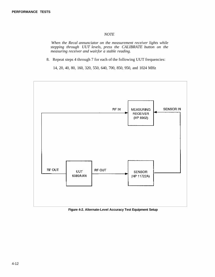
PERFORMANCE TESTS
NOTE
When the Recal annunciator on the measurement receiver lights whilestepping through UUT levels, press the CALIBRATE button on themeasuring receiver and wait for a stable reading.
8. Repeat steps 4 through 7 for each of the following UUT frequencies:
14, 20, 40, 80, 160, 320, 550, 640, 700, 850, 950, and 1024 MHz
Figure 4-2. Alternate-Level Accuracy Test Equipment Setup
4-12
PERFORMANCE TESTS
FLATNESS TEST 4-10.
A power meter and sensor are used to verify the high level flatness of the instrument.
REQUIREMENT:
Amplifier flatness is:
< ± 1 dB at +10 dBm over the frequency range of 0.5 to 1024 MHz.
TEST EQUIPMENT:
• Power meter• Power sensor (high level)
REMARKS:
If the UUT fails this test, calibration (see Section 3) or repair (see Section 6) isnecessary. If no power-on status codes are present, likely problem areas needing repairinclude the A8 Output PCA, the A21 Attenuator PCA, or the A7 Relay Driver PCA.
PROCEDURE:
1. Calibrate and zero the power meter.
2. Connect the power sensor to the instrument RF Output.
3. Program the instrument to SPCL 909 and then to 0.5 MHz and + 10 dBm.
4. The power meter should read + 10 ±1 dBm.
5. Repeat step 4 for the following frequencies:
a. 0.5 to 2.0 MHz in 0.1 MHz steps
b. 2.0 to 20.0 MHz in 1.0 MHz steps
c. 20.0 to 200.0 MHz in 10.0 MHz steps
d. 200.0 to 1024.0 MHz in 20.0 MHz steps
4-13
PERFORMANCE TESTS
OUTPUT LEAKAGE TEST 4-11.
The output signal leakage is verified using a 1-inch diameter, two-turn loop. Theinduced signal is measured with an RF Spectrum Analyzer and compared to a l-μVreference established at each reference frequency. The two-turn loop must be 1 inchaway from any surface of the UUT.
REQUIREMENT:
Radiated emissions induce < 1 μV of the signal generator's output signal.
TEST EQUIPMENT:
0.1- to 1050-GHz amplifierRF spectrum analyzerTwo-turn loopType-N terminationA screen room may be required, depending on the RF environment.
REMARKS:
If the UUT fails this test, a feed-through filter is probably broken or an impropermechanical assembly (i.e., loose screws and/or damaged or misplaced gaskets) isindicated.
PROCEDURE:
1. Connect the UUT RF OUTPUT to the wideband amplifier input, and connect thewideband amplifier output to the RF spectrum analyzer input. Use well shieldedcables to avoid leakage that could affect the measurement.
2. Program the UUT to SPCL 909.
3. Program the UUT to -107 dBm.
4. Adjust the RF spectrum analyzer to display the UUT signal for a convenientreference. Make this adjustment using a vertical scale of 10 dB/division, aresolution bandwidth of 3 kHz, and a span/division of 5 kHz/division.
5. Disconnect the wideband amplifier from the UUT and terminate UUT OUTPUTwith the type-N termination.
6. Connect the two-turn loop to the wideband amplifier input.
7. Program the UUT to +13 dBm.
8. Verify that the leakage indicated by the RF spectrum analyzer is less than -107 dBm(1 μV) by moving the two-turn loop over the UUT surface at a distance of 1 inch.
9. Repeat steps 3 through 8 at 14, 20, 40, 80, 160, 320, 550, 640, 700, 850, 950, and1024 MHz.
4-14
PERFORMANCE TESTS
HARMONIC AND LINE-RELATED SPURIOUS TEST 4-12.
The Harmonic and Line-Related Spurious Test uses an RF spectrum analyzer tocompare the level of the harmonic signal and close-in spurious signals to the desiredsignal at various programmed frequencies.
REQUIREMENTS:
• RF harmonics: <-30 dBc for levels <= +13 dBm.• Power line spurious signals: -40 dBc (signals within 15 kHz of carrier)
TEST EQUIPMENT:
• RF Spectrum Analyzer
PROCEDURE:
1. Connect the UUT RF OUTPUT to the RF spectrum analyzer input.
2. Program the UUT to SPCL 909.
3. Program the UUT to +13 dBm and 0.5 MHz.
4. Set the RF spectrum analyzer controls to display the UUT output signal and itsharmonics (at least three harmonics wherever possible). Be careful not to overloadthe analyzer input. Overloading the RF spectrum analyzer causes it to generateharmonics, thus invalidating the test.
5. Verify that all the harmonics are more than 30 dB below the fundamental signal.
6. Program the UUT to 7.0 dBm.
7. Verify that all the harmonics are more than 30 dB below the fundamental signal forthe following frequencies:
14, 20, 40, 80, 160, 320, 550, 640, 700, 850, 950, and 1056 MHz.
8. Set the RF spectrum analyzer to display the UUT output signal with a 2-kHz spanand 10-Hz resolution. Verify that all spurious signals are below -40 dBc forfrequencies listed in step 7.
9. Set the RF spectrum analyzer to display the UUT output signal with a 50-kHz spanand 30-Hz resolution. Verify that all spurious signals are below -40 dBc forfrequencies listed in step 7.
4-15
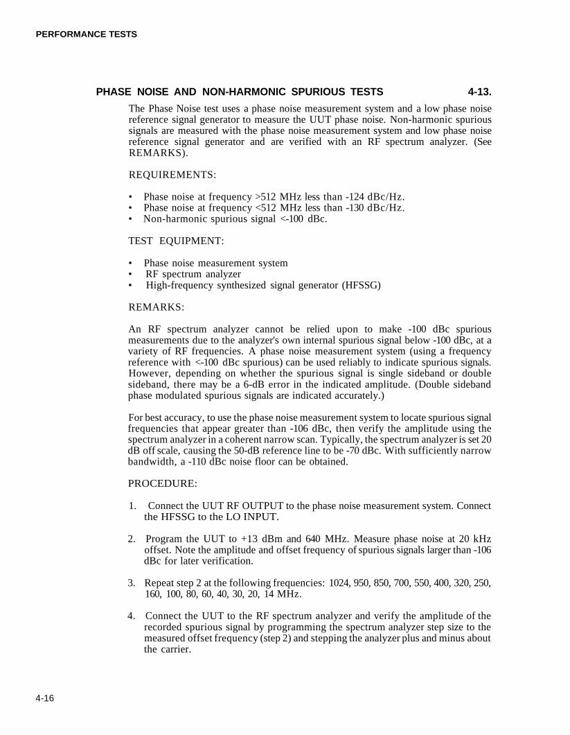
PERFORMANCE TESTS
PHASE NOISE AND NON-HARMONIC SPURIOUS TESTS 4-13.
The Phase Noise test uses a phase noise measurement system and a low phase noisereference signal generator to measure the UUT phase noise. Non-harmonic spurioussignals are measured with the phase noise measurement system and low phase noisereference signal generator and are verified with an RF spectrum analyzer. (SeeREMARKS).
REQUIREMENTS:
• Phase noise at frequency >512 MHz less than -124 dBc/Hz.• Phase noise at frequency <512 MHz less than -130 dBc/Hz.• Non-harmonic spurious signal <-100 dBc.
TEST EQUIPMENT:
• Phase noise measurement system• RF spectrum analyzer• High-frequency synthesized signal generator (HFSSG)
REMARKS:
An RF spectrum analyzer cannot be relied upon to make -100 dBc spuriousmeasurements due to the analyzer's own internal spurious signal below -100 dBc, at avariety of RF frequencies. A phase noise measurement system (using a frequencyreference with <-100 dBc spurious) can be used reliably to indicate spurious signals.However, depending on whether the spurious signal is single sideband or doublesideband, there may be a 6-dB error in the indicated amplitude. (Double sidebandphase modulated spurious signals are indicated accurately.)
For best accuracy, to use the phase noise measurement system to locate spurious signalfrequencies that appear greater than -106 dBc, then verify the amplitude using thespectrum analyzer in a coherent narrow scan. Typically, the spectrum analyzer is set 20dB off scale, causing the 50-dB reference line to be -70 dBc. With sufficiently narrowbandwidth, a -110 dBc noise floor can be obtained.
PROCEDURE:
1. Connect the UUT RF OUTPUT to the phase noise measurement system. Connectthe HFSSG to the LO INPUT.
2. Program the UUT to +13 dBm and 640 MHz. Measure phase noise at 20 kHzoffset. Note the amplitude and offset frequency of spurious signals larger than -106dBc for later verification.
3. Repeat step 2 at the following frequencies: 1024, 950, 850, 700, 550, 400, 320, 250,160, 100, 80, 60, 40, 30, 20, 14 MHz.
4. Connect the UUT to the RF spectrum analyzer and verify the amplitude of therecorded spurious signal by programming the spectrum analyzer step size to themeasured offset frequency (step 2) and stepping the analyzer plus and minus aboutthe carrier.
4-16
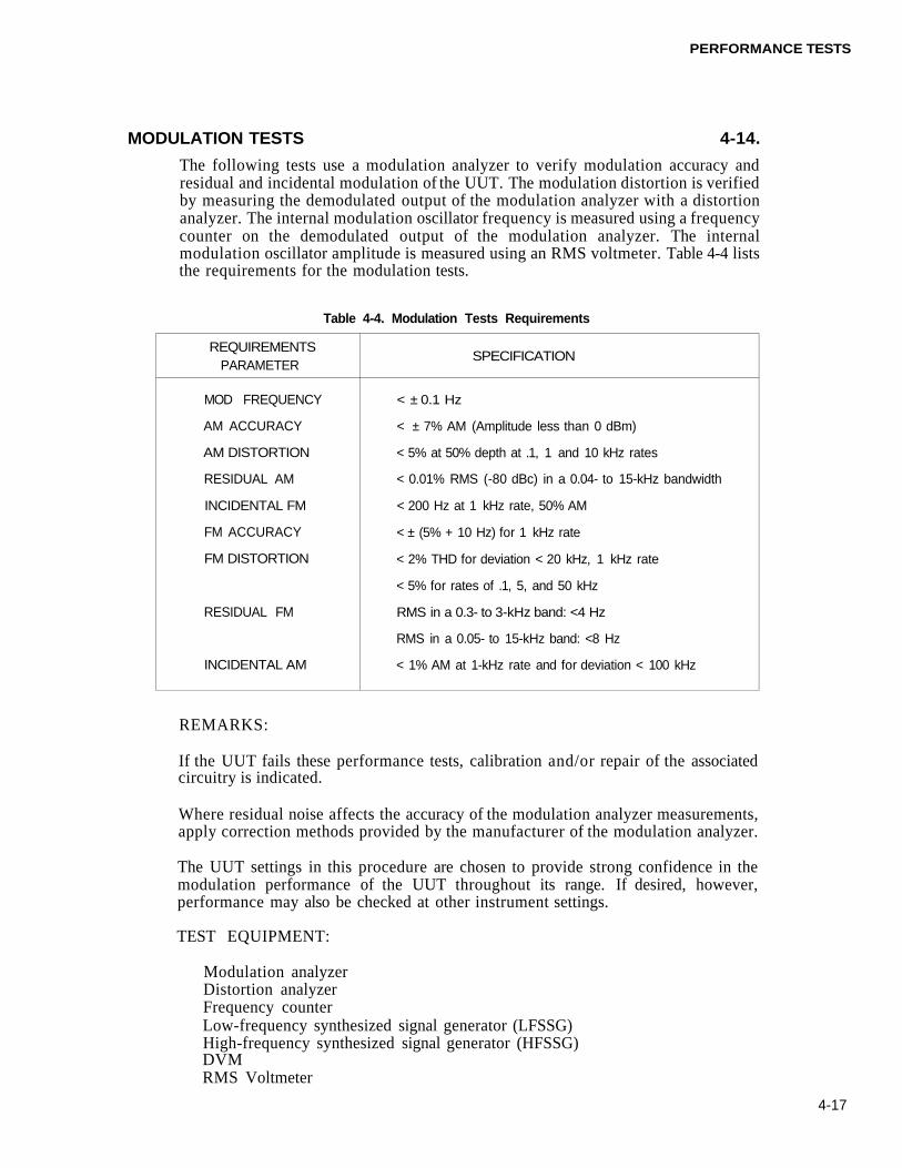
PERFORMANCE TESTS
MODULATION TESTS 4-14.
The following tests use a modulation analyzer to verify modulation accuracy andresidual and incidental modulation of the UUT. The modulation distortion is verifiedby measuring the demodulated output of the modulation analyzer with a distortionanalyzer. The internal modulation oscillator frequency is measured using a frequencycounter on the demodulated output of the modulation analyzer. The internalmodulation oscillator amplitude is measured using an RMS voltmeter. Table 4-4 liststhe requirements for the modulation tests.
Table 4-4. Modulation Tests Requirements
REMARKS:
If the UUT fails these performance tests, calibration and/or repair of the associatedcircuitry is indicated.
Where residual noise affects the accuracy of the modulation analyzer measurements,apply correction methods provided by the manufacturer of the modulation analyzer.
The UUT settings in this procedure are chosen to provide strong confidence in themodulation performance of the UUT throughout its range. If desired, however,performance may also be checked at other instrument settings.
TEST EQUIPMENT:
Modulation analyzerDistortion analyzerFrequency counterLow-frequency synthesized signal generator (LFSSG)High-frequency synthesized signal generator (HFSSG)DVMRMS Voltmeter
4-17
REQUIREMENTSPARAMETER
MOD FREQUENCY
AM ACCURACY
AM DISTORTION
RESIDUAL AM
INCIDENTAL FM
FM ACCURACY
FM DISTORTION
RESIDUAL FM
INCIDENTAL AM
SPECIFICATION
< ± 0.1 Hz
< ± 7% AM (Amplitude less than 0 dBm)
< 5% at 50% depth at .1, 1 and 10 kHz rates
< 0.01% RMS (-80 dBc) in a 0.04- to 15-kHz bandwidth
< 200 Hz at 1 kHz rate, 50% AM
< ± (5% + 10 Hz) for 1 kHz rate
< 2% THD for deviation < 20 kHz, 1 kHz rate
< 5% for rates of .1, 5, and 50 kHz
RMS in a 0.3- to 3-kHz band: <4 Hz
RMS in a 0.05- to 15-kHz band: <8 Hz
< 1% AM at 1-kHz rate and for deviation < 100 kHz
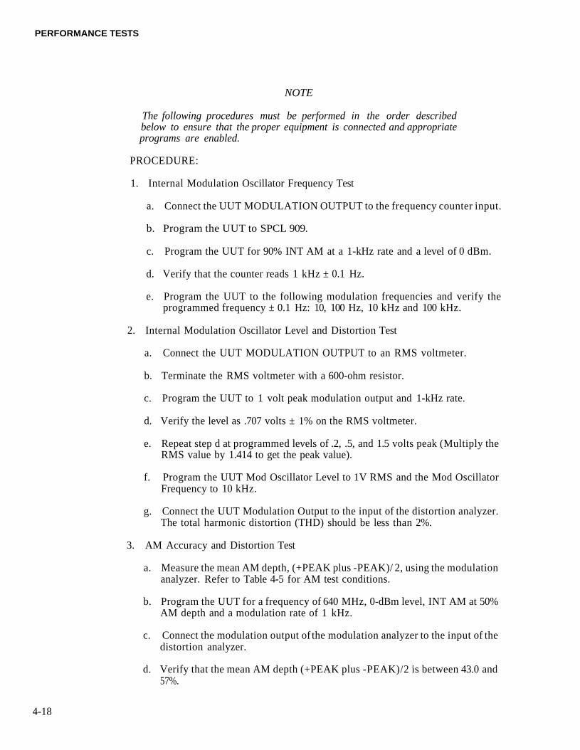
PERFORMANCE TESTS
NOTE
The following procedures must be performed in the order describedbelow to ensure that the proper equipment is connected and appropriateprograms are enabled.
PROCEDURE:
1. Internal Modulation Oscillator Frequency Test
a. Connect the UUT MODULATION OUTPUT to the frequency counter input.
b. Program the UUT to SPCL 909.
c. Program the UUT for 90% INT AM at a 1-kHz rate and a level of 0 dBm.
d. Verify that the counter reads 1 kHz ± 0.1 Hz.
e. Program the UUT to the following modulation frequencies and verify theprogrammed frequency ± 0.1 Hz: 10, 100 Hz, 10 kHz and 100 kHz.
2. Internal Modulation Oscillator Level and Distortion Test
a. Connect the UUT MODULATION OUTPUT to an RMS voltmeter.
b. Terminate the RMS voltmeter with a 600-ohm resistor.
c. Program the UUT to 1 volt peak modulation output and 1-kHz rate.
d. Verify the level as .707 volts ± 1% on the RMS voltmeter.
e. Repeat step d at programmed levels of .2, .5, and 1.5 volts peak (Multiply theRMS value by 1.414 to get the peak value).
f. Program the UUT Mod Oscillator Level to 1V RMS and the Mod OscillatorFrequency to 10 kHz.
g. Connect the UUT Modulation Output to the input of the distortion analyzer.The total harmonic distortion (THD) should be less than 2%.
3. AM Accuracy and Distortion Test
a. Measure the mean AM depth, (+PEAK plus -PEAK)/ 2, using the modulationanalyzer. Refer to Table 4-5 for AM test conditions.
b. Program the UUT for a frequency of 640 MHz, 0-dBm level, INT AM at 50%AM depth and a modulation rate of 1 kHz.
c. Connect the modulation output of the modulation analyzer to the input of thedistortion analyzer.
d. Verify that the mean AM depth (+PEAK plus -PEAK)/2 is between 43.0 and57%.
4-18
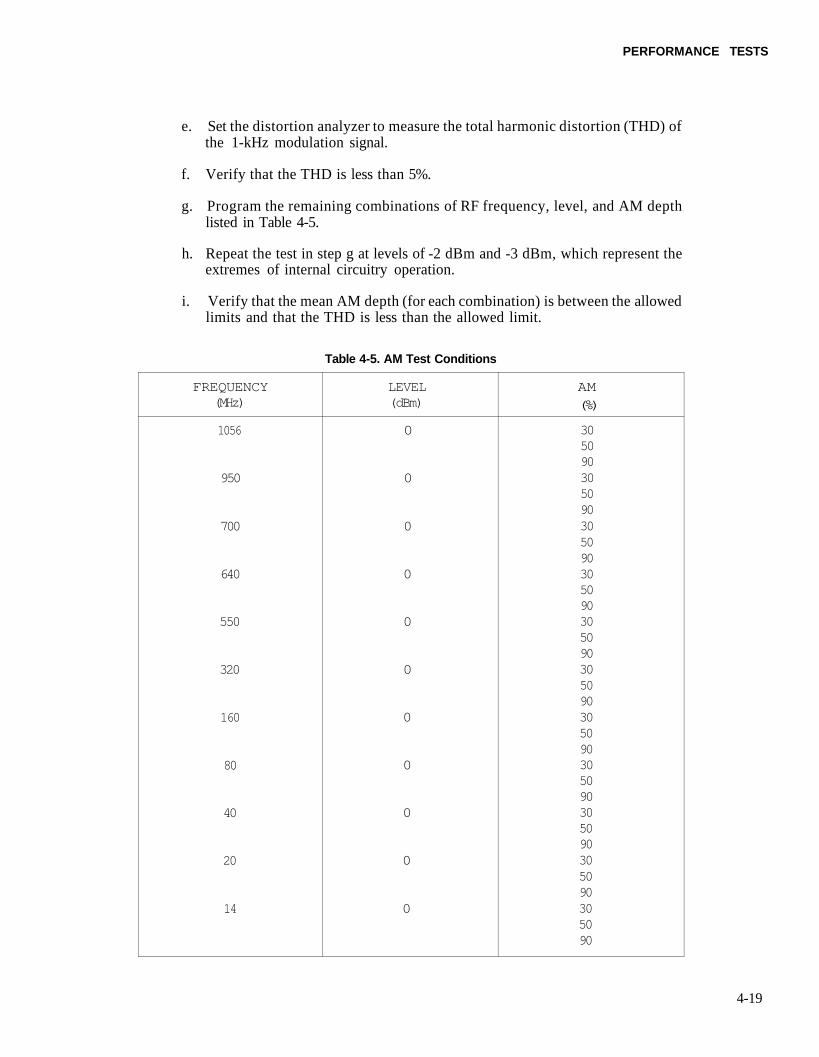
PERFORMANCE TESTS
e. Set the distortion analyzer to measure the total harmonic distortion (THD) ofthe 1-kHz modulation signal.
f. Verify that the THD is less than 5%.
g. Program the remaining combinations of RF frequency, level, and AM depthlisted in Table 4-5.
h. Repeat the test in step g at levels of -2 dBm and -3 dBm, which represent theextremes of internal circuitry operation.
i. Verify that the mean AM depth (for each combination) is between the allowedlimits and that the THD is less than the allowed limit.
Table 4-5. AM Test Conditions
FREQUENCY(MHz)
1056
950
700
640
550
320
160
80
40
20
14
LEVEL(dBm)
0
0
0
0
0
0
0
0
0
0
0
AM(%)
305090305090305090305090305090305090305090305090305090305090305090
4-19
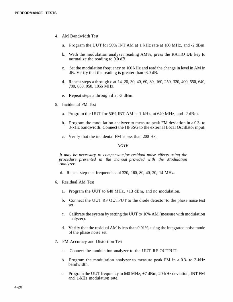
PERFORMANCE TESTS
4. AM Bandwidth Test
a. Program the UUT for 50% INT AM at 1 kHz rate at 100 MHz, and -2 dBm.
b. With the modulation analyzer reading AM%, press the RATIO DB key tonormalize the reading to 0.0 dB.
c. Set the modulation frequency to 100 kHz and read the change in level in AM indB. Verify that the reading is greater than -3.0 dB.
d. Repeat steps a through c at 14, 20, 30, 40, 60, 80, 160, 250, 320, 400, 550, 640,700, 850, 950, 1056 MHz.
e. Repeat steps a through d at -3 dBm.
5. Incidental FM Test
a. Program the UUT for 50% INT AM at 1 kHz, at 640 MHz, and -2 dBm.
b. Program the modulation analyzer to measure peak FM deviation in a 0.3- to3-kHz bandwidth. Connect the HFSSG to the external Local Oscillator input.
c. Verify that the incidental FM is less than 200 Hz.
NOTE
It may be necessary to compensate for residual noise effects using theprocedure presented in the manual provided with the ModulationAnalyzer.
d. Repeat step c at frequencies of 320, 160, 80, 40, 20, 14 MHz.
6. Residual AM Test
a. Program the UUT to 640 MHz, +13 dBm, and no modulation.
b. Connect the UUT RF OUTPUT to the diode detector to the phase noise testset.
c. Calibrate the system by setting the UUT to 10% AM (measure with modulationanalyzer).
d. Verify that the residual AM is less than 0.01%, using the integrated noise modeof the phase noise set.
7. FM Accuracy and Distortion Test
a. Connect the modulation analyzer to the UUT RF OUTPUT.
b. Program the modulation analyzer to measure peak FM in a 0.3- to 3-kHzbandwidth.
c. Program the UUT frequency to 640 MHz, +7 dBm, 20-kHz deviation, INT FMand 1-kHz modulation rate.
4-20
PERFORMANCE TESTS
d. Set the distortion analyzer to measure distortion at 1 kHz.
e. Verify that the modulation analyzer reading is between 19 and 21 kHz, and thatthe THD is less than 2%. Repeat at deviations of 5 and 10 kHz. Verify that themodulation analyzer reading is within ± 5% of programmed value. (See thefollowing NOTE).
f. Program the UUT to deviation of 50, 100, and 200 kHz.
g. Verify that the modulation analyzer reading is the deviation programmed ± 5%and that the distortion is less than 5%.
h. Repeat steps d through g with the modulation rate set to 100 Hz. Verifydistortion only.
NOTE
Change the modulation analyzer bandwidth and distortion analyzerfrequency appropriately for modulation frequency for steps h through p.
i. Repeat steps d through g with modulation rate set to 50 kHz. Verify distortiononly.
j. Program UUT to 40-MHz frequency, 25-kHz deviation and 1-kHz INTmodulation frequency.
k. Verify that the Modulation Analyzer reading is between 23.75 and 26.25 andthat the distortion is less than 5%.
1. Program the UUT to deviation of 50, 100, 200, and 250 kHz.
m. Verify that the modulation analyzer readings correspond to that programmed± 5% and that the distortion is less than 5%.
n. Repeat steps j through m with the modulation rate set to 100 Hz. Verifydistortion only.
o. Repeat steps j through m with the modulation rate set to 50 kHz. Verifydistortion only.
p. Set the modulation rate to 100 kHz with 250 kHz deviation. Verify thatmeasured deviation is greater than 177 kHz (3 dB bandwidth).
NOTE
It may be necessary to compensate for residual noise effects using theprocedure presented in the manual provided with the ModulationAnalyzer.
8. øM Accuracy Test
a. Connect the LFSSG output to the UUT MOD INPUT connector and theDVM (use a BNC T connector).
4-21
PERFORMANCE TESTS
b. Program the UUT to SPCL 909, EXT øM, and 10 radians phase deviation.
c. Program the LFSSG for .3 kHz and .7071V RMS, as measured by the DVM.
d. Program the modulation analyzer to measure øM + peak in a 50-Hz to 15-kHzbandwidth.
e. Verify that the modulation analyzer reading is between 9.5 and 10.5 radians.
f. Program the LFSSG for 10 kHz and 0.7071V RMS, as measured by the DVM.
g. Verify that the modulation analyzer reading is between 8.5 and 10.0 radians. (3dB bandwidth, 15 kHz).
NOTE
It may be necessary to compensate for residual noise effects using theprocedure presented in the manual provided with the ModulationAnalyzer.
9. Incidental AM Test
a. Program the UUT for 100-kHz deviation, INT FM on at 1 kHz, EXT FM off, alevel of +7 dBm, and a frequency of 14 MHz.
b. Program the modulation analyzer to measure peak AM in a 0.3- to 3-kHzbandwidth.
c. Verify that the incidental AM is less than 1%.
d. Repeat steps a through cat frequencies of 20, 30, 40, 60, 80, 100, 160, 250, 320,400, 550, 640, 700, 850, 950, 1056 MHz.
10. Residual FM Test
a. Program the UUT for a frequency of 640 MHz and no modulation.
b. Program the HFSSG to 641.5 MHz and +1.0 dBm.
c. Connect the HFSSG output to the modulation analyzer external LO inputconnector.
d. Program the modulation analyzer to measure average FM in the 50-Hz to15-kHz band width.
e. Verify that the modulation analyzer reading is less than 8 Hz RMS.
f. Verify that the modulation analyzer reading is less than 8 Hz average at thefollowing UUT frequencies: 1024, 950, 850, 700, 640, 550, 400, 320, 160, 100,80, 60, 40, 30, 20, 14.
Program the external LO to a frequency 1.5 MHz higher than the UUTfrequency in each case.
4-22
PERFORMANCE TESTS
VOLTAGE STANDING-WAVE RATIO (VSWR) TESTS 4-15.
The Voltage Standing-Wave ratio (VSWR) tests use a VSWR bridge and a spectrumanalyzer to verify VSWR of the UUT.
REQUIREMENTS:
The output VSWR is less than 1.5:1 for output levels < -10 dBm; < 2.5:1 elsewhere.
EQUIPMENT REQUIRED:
• VSWR bridge• RF spectrum analyzer• High-frequency synthesized signal generator (FSSG)
REMARKS:
The UUT settings in this procedure are chosen to provide confidence in the VSWRperformance of the UUT throughout its range. However, performance also may bechecked at other levels.
VSWR problems are most likely to involve the A8 Output PCA or the A21 AttenuatorPCA.
NOTE
The following procedures must be done in sequential order to ensure thatthe proper equipment is connected and appropriate programs areenabled.
PROCEDURE:
1. Low-Level Test
a. With the UUT on, program the UUT to SPCL 909.
b. Program the UUT to 640 MHz at -10 dBm.
c. Select the fixed range special function on the UUT by pressing
d. Using the EDIT function on the UUT, edit the amplitude to -30 dBm. Verifythat the UNCAL annunciator illuminates.
NOTE
This procedure leaves the output attenuators set as they would be for a -10dBm output level, but uses the electronic control to turn down the RFlevel coming out of the UUT.
e. Connect the UUT to the Device Under Test port of the VSWR bridge.
f. Connect the RF spectrum analyzer to the RF OUT port of the VSWR bridge.
4-23
PERFORMANCE TESTS
g. Connect the HFSSG to the RF IN port of the VSWR Bridge,
h. Program the HFSSG to 10 MHz at +13 dBm.
i. Set the RF spectrum analyzer to display approximately 10 to 1024 MHz andset the reference level to +10 dBm.
j. Step the HFSSG from 10 to 1024 MHz in 10-MHz steps. Locate the frequencyat which the reflected signal (displayed by the RF spectrum analyzer) ismaximum and record this level. This is the point with worst-case VSWR.
k. Disconnect the UUT from the VSWR Bridge and record the new level.
1. Calculate the return loss (difference) between the two recorded levels. Thedifference must be at least 14 dB (14 dB of return loss = 1.5:1 VSWR).
2. High-Level Test
a. Program the UUT to +10 dBm.
b. Select the special function fixed range on the UUT by pressing
c. Using the EDIT function on the UUT, edit the amplitude to -30 dBm.
d. Connect the UUT to the Device Under Test port of the VSWR bridge.
e. Step the HFSSG from 10 to 1024 MHz in 10-MHz steps. Locate the frequencyat which the reflected signal is maximum and record this level.
f. Disconnect the UUT from the VSWR bridge and record the new level.
g. Calculate the return loss between the two recorded levels. The difference mustbe at least 7.5 dB (7.5 dB of return loss = 2.5:1 VSWR).
PULSE TESTS 4-16.
The Pulse Tests check the static and dynamic operation of pulse modulation.
REQUIREMENTS:
Proper pulse operation is tested by checking that:
• Static on/off ratio greater than 35 dB• Dynamic rise and fall time <1 microsecond.
TEST EQUIPMENT:
RF spectrum analyzerPulse generatorPower meterPower sensor (high-level)50-Ohm terminationOscilloscopeDetector
4-24
PERFORMANCE TESTS
NOTE
The following procedures must be performed in the order describedbelow to ensure that the proper equipment is connected and appropriateprograms are enabled.
PROCEDURE:
1. Static Test
a. Program the UUT to 1024 MHz and +10 dBm.
b. Connect a 50-ohm termination to the pulse modulation input connector.
c. Connect the UUT RF OUTPUT to the RF spectrum analyzer input.
d. Set the RF spectrum analyzer controls to display the output of the UUT using aspan of approximately 0.5 MHz to 1024 MHz.
e. Activate pulse modulation by pressing the External Pulse key on the UUT.
f. Observe the level change on the RF spectrum analyzer. The change shouldexceed 35 dB.
g. Deactivate external pulse by pressing the External Pulse key on the UUT, andrepeat steps d through f for UUT frequencies of 950, 850, 700, 640, 550, 400,320, 250, 160, 100, 80, 60, 40, 30, 20, 14 MHz.
2. Dynamic Test
a. Program the UUT to 640 MHz, +10 dBm, and external pulse modulation.
b. Connect the pulse generator to the UUT pulse input connector.
c. Set the pulse generator to a repetition rate of 50 kHz, +3V pulse level, androughly a 50% duty cycle.
d. Connect the output of the UUT to the detector.
e. Terminate the detector into 50 ohms at the oscilloscope input.
f. Set the time base of the oscilloscope to 1.0 microsecond/division.
g. Use the oscilloscope channel to invert the detector output signal,
h. Trigger the oscilloscope on this signal.
i. Set the variable position and gain on the oscilloscope so that the signal extendsfrom 0% to 100% on the graticule.
j. Measure the rise/fall time from the 90% to the 10% coordinates,
k. Verify that the rise/fall time is < 1 microsecond.
4-25
PERFORMANCE TESTS
1. Repeat steps f through k at 320 MHz. The time base of the oscilloscope shouldalso be readjusted if necessary.
m. Remove the detector and reconnect the UUT directly into the oscilloscope,
n. Change the repetition rate of the Pulse Generator to .5 MHz.
o. Verify that the rise/fall time is < 1 microsecond for RF frequencies of 100 and50 MHz.
4-26
Some semiconductors and custom IC's can bedamaged by electrostatic discharge duringhandling. This notice explains how you canminimize the chances of destroying such devicesby:1. Knowing that there is a problem.2. Learning the guidelines for handling them.3. Using the procedures, and packaging and
bench techniques that are recommended.
The Static Sensitive (S.S.) devices are identified in the Fluke technical manual parts list with the symbol
The following practices should be followed to minimize damage to S.S. devices.
1. MINIMIZE HANDLING
2. KEEP PARTS IN ORIGINAL CONTAINERSUNTIL READY FOR USE.
3. DISCHARGE PERSONAL STATIC BEFOREHANDLING DEVICES. USE A HIGH RESIS-TANCE GROUNDING WRIST STRAP.
4. HANDLE S.S. DEVICES BY THE BODY
Page 1 of 2
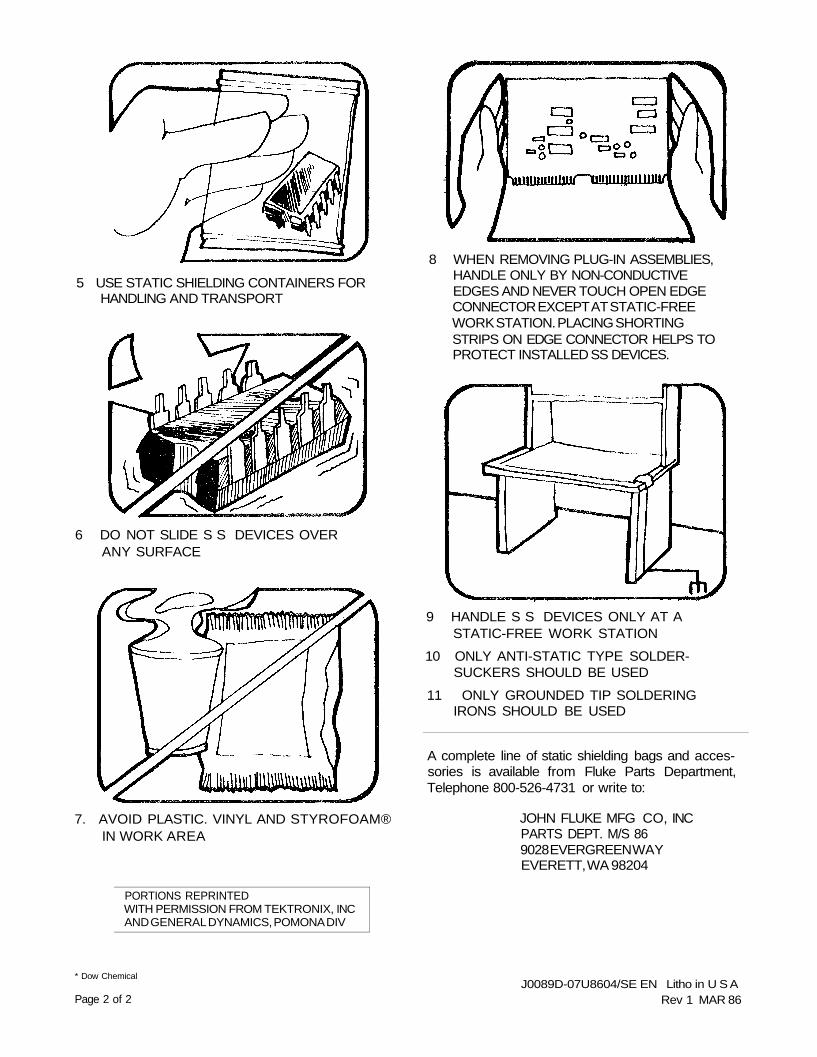
5 USE STATIC SHIELDING CONTAINERS FORHANDLING AND TRANSPORT
6 DO NOT SLIDE S S DEVICES OVERANY SURFACE
7. AVOID PLASTIC. VINYL AND STYROFOAM®IN WORK AREA
8 WHEN REMOVING PLUG-IN ASSEMBLIES,HANDLE ONLY BY NON-CONDUCTIVEEDGES AND NEVER TOUCH OPEN EDGECONNECTOR EXCEPT AT STATIC-FREEWORK STATION. PLACING SHORTINGSTRIPS ON EDGE CONNECTOR HELPS TOPROTECT INSTALLED SS DEVICES.
9 HANDLE S S DEVICES ONLY AT ASTATIC-FREE WORK STATION
10 ONLY ANTI-STATIC TYPE SOLDER-SUCKERS SHOULD BE USED
11 ONLY GROUNDED TIP SOLDERINGIRONS SHOULD BE USED
A complete line of static shielding bags and acces-sories is available from Fluke Parts Department,Telephone 800-526-4731 or write to:
JOHN FLUKE MFG CO, INCPARTS DEPT. M/S 869028 EVERGREEN WAYEVERETT, WA 98204
PORTIONS REPRINTEDWITH PERMISSION FROM TEKTRONIX, INCAND GENERAL DYNAMICS, POMONA DIV
* Dow Chemical
Page 2 of 2J0089D-07U8604/SE EN Litho in U S A
Rev 1 MAR 86
Section 5Access Procedures
INTRODUCTION AND SAFETY 5-1.
Section 5 describes the general access procedures for the following major assemblies:
Front Panel SectionRear Panel SectionA2 Coarse Loop PCAA3 Sub-Synthesizer VCO PCAA4 Sub-Synthesizer PCAA5 Coarse Loop VCO PCAA6 Mod Oscillator PCAA8 Output PCAA9 Sum Loop VCO PCAA10 Premodulator PCAA11 Modulation Control PCAA12 Sum Loop PCAA13 Controller PCAA14 FM PCAA20 Attenuator/RPP AssemblyA22 Delay Line Assembly
Access to other assemblies does not require description.
5-1
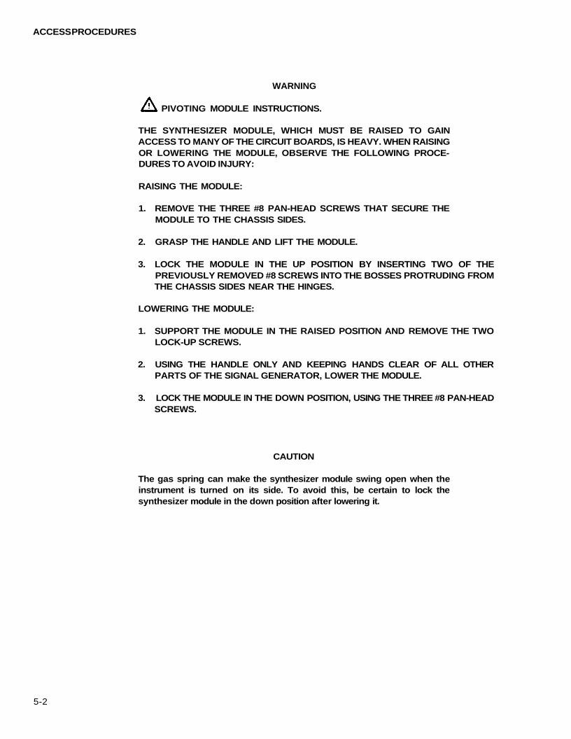
ACCESS PROCEDURES
WARNING
PIVOTING MODULE INSTRUCTIONS.
THE SYNTHESIZER MODULE, WHICH MUST BE RAISED TO GAINACCESS TO MANY OF THE CIRCUIT BOARDS, IS HEAVY. WHEN RAISINGOR LOWERING THE MODULE, OBSERVE THE FOLLOWING PROCE-DURES TO AVOID INJURY:
RAISING THE MODULE:
1. REMOVE THE THREE #8 PAN-HEAD SCREWS THAT SECURE THEMODULE TO THE CHASSIS SIDES.
2. GRASP THE HANDLE AND LIFT THE MODULE.
3. LOCK THE MODULE IN THE UP POSITION BY INSERTING TWO OF THEPREVIOUSLY REMOVED #8 SCREWS INTO THE BOSSES PROTRUDING FROMTHE CHASSIS SIDES NEAR THE HINGES.
LOWERING THE MODULE:
1. SUPPORT THE MODULE IN THE RAISED POSITION AND REMOVE THE TWOLOCK-UP SCREWS.
2. USING THE HANDLE ONLY AND KEEPING HANDS CLEAR OF ALL OTHERPARTS OF THE SIGNAL GENERATOR, LOWER THE MODULE.
3. LOCK THE MODULE IN THE DOWN POSITION, USING THE THREE #8 PAN-HEADSCREWS.
CAUTION
The gas spring can make the synthesizer module swing open when theinstrument is turned on its side. To avoid this, be certain to lock thesynthesizer module in the down position after lowering it.
5-2
ACCESS PROCEDURES
LOCATION OF MAJOR ASSEMBLIES 5-2.
The location of the major assemblies is illustrated in Section 7.
Information on exchanging modules is presented in Section 6, "CIRCUITDESCRIPTIONS, TROUBLESHOOTING, AND ALIGNMENT".
ACCESS INSTRUCTIONS 5-3.
Access instructions for each assembly of the 6080A/AN signal generator are providedin the following paragraphs. Before performing any disassembly of the signalgenerator, remove the power cord from the rear panel power receptacle and remove theexterior top and bottom instrument covers.
To install the assemblies, reverse the disassembly steps. Be certain the pin connectorsand filter sockets are straight when replacing a printed circuit assembly (PCA). Takecare that the PCA pulls and RF cables are not pinched between the modules andmodule covers.
Removing the Front Panel Section 5-4.
1. Remove the two (#6) pan-head screws that attach the RF connector bracket to theoutput module near the attenuator assembly A20. One screw is accessible from thetop of the instrument, the other from the bottom.
2. Disconnect the RF Output cable W1 from the type-N RF output connector J1.
3. Remove the decals from both front panel handles. (Removing the decals ruinsthem. Attach new decals when reassembling to maintain proper instrumentappearance. The part number for the decal is listed in Section 7.)
4. Remove the five flat-head screws from each front panel handle, and slide the frontpanel forward.
5. Disconnect the power ribbon cable W20 and the two controller ribbon cables W18and W36 from the front panel display board Al.
6. Disconnect the inner part of the BNC connectors on the Mod Input and ModOutput cables W2, W3, W4, and W5.
Removing the Rear Panel Section 5-5.
1. Disconnect the synthesizer and output module power cables W22 and W23, andthe front panel power cable W20 from the A15 Power Supply PCA.
2. Disconnect the controller-IEEE ribbon cable W17 from the A16 IEEE PCA.
3. Disconnect the Ref In and Ref Out RF cables W6 and W7 from the synthesizermodule.
4. Remove the decals for both rear panel handles. (Removing the decals ruins them.Attach new decals when reassembling to maintain proper instrument appearance.The part number for the decal is listed in Section 7.)
5. Remove the five flat-head screws from each handle. The rear panel section can nowbe removed.
5-3
ACCESS PROCEDURES
Removing the A2 Coarse Loop PCA 5-6.
WARNING
THE SYNTHESIZER MODULE, WHICH MUST BE RAISED TO GAINACCESS TO THE A2 COARSE LOOP PCA, IS HEAVY. WHEN RAISING ORLOWERING THE MODULE, OBSERVE THE PROCEDURE DESCRIBEDUNDER THE HEADING "INTRODUCTION AND SAFETY" EARLIER INSECTION 5.
1. Disconnect RF cables W6, W7, and W15 from the connectors at the rear of thesynthesizer module, and remove the nuts and lockwashers from the connectors.
2. Raise the synthesizer module.
3. Remove the #6 screws holding the bottom synthesizer module cover, and removethe cover.
4. Remove the plug-in capacitor C1 and resistor R1 which are between the A22 DelayCable assembly and the A2 Coarse Loop PCA.
NOTE
When reinstalling Cl, be certain to put it between J1 on the A22 DelayCable assembly and J9 on the A2 Coarse Loop. J2 on A22 and J10 on theA2 PCA are not used.
5. Remove the #6 screws holding the heatsinks on U305 and U310, and remove theheatsinks.
6. Remove the #6 screws holding the PCA.
7. Carefully remove the A2 Coarse Loop PCA.
Removing the A3 Sub-Synthesizer VCO PCA 5-7.
WARNING
THE SYNTHESIZER MODULE, WHICH MUST BE RAISED TO GAINACCESS TO THE A3 SUB-SYNTHESIZER VCO PCA, IS HEAVY. WHENRAISING OR LOWERING THE MODULE, OBSERVE THE PROCEDUREDESCRIBED UNDER THE HEADING "INTRODUCTION AND SAFETY"EARLIER IN SECTION 5.
1. Disconnect RF cable W13 from the connector at the front of the synthesizermodule, and remove the nut and lockwasher from the connector.
2. Raise the synthesizer module.
3. Remove the #6 screws holding the bottom synthesizer module cover, and removethe cover.
4. Remove the #6 screws holding the PCA.
5. Carefully remove the A3 Sub-Synthesizer VCO PCA.
5-4
ACCESS PROCEDURES
Removing the A4 Sub-Synthesizer PCA 5-8.
1. Remove the #6 screws holding the top synthesizer module cover, and remove thecover. (The #10 screws are adjustment-access screws and need not be removed).
2. Remove the #6 screws holding the PCA.
3. Carefully remove the A4 Sub-Synthesizer PCA.
Removing the A5 Coarse Loop VCO PCA 5-9.
WARNING
THE SYNTHESIZER MODULE, WHICH MUST BE RAISED TO GAINACCESS TO THE A5 COARSE LOOP VCO PCA, IS HEAVY. WHEN RAISINGOR LOWERING THE MODULE, OBSERVE THE PROCEDURE DESCRIBEDUNDER THE HEADING "INTRODUCTION AND SAFETY" EARLIER INSECTION 5.
1. Raise the synthesizer module.
2. Disconnect RF cable W14 from the connector at the front of the synthesizermodule, and remove the nut and lockwasher from the connector.
3. Lower the synthesizer module.
4. Remove the #6 screws holding the top synthesizer module cover, and remove thecover. (The #10 screws are adjustment-access screws and need not be removed).
5. Remove the #6 screws holding the PCA.
6. Carefully remove the A5 Coarse Loop VCO PCA.
Removing the A6 Mod Oscillator PCA 5-10.
1. Remove the #6 screws holding the top synthesizer module cover, and remove thecover. (The #10 screws are adjustment-access screws and need not be removed).
2. Remove the #6 screws holding the PCA.
3. Carefully remove the A6 Mod Oscillator PCA.
Removing the A 8 Output P C A 5 - 1 1 .
WARNING
THE SYNTHESIZER MODULE, WHICH MUST BE RAISED TO GAINACCESS TO THE A8 OUTPUT PCA, IS HEAVY. WHEN RAISING ORLOWERING THE MODULE, OBSERVE THE PROCEDURE DESCRIBEDUNDER THE HEADING "INTRODUCTION AND SAFETY" EARLIER INSECTION 5.
1. Raise the synthesizer module.
2. Disconnect RF cable W15 from the connector at the back of the output module,and remove the nut and lockwasher from the connector.
3. Lower the synthesizer module.
5-5
ACCESS PROCEDURES
4. Remove the #6 screws holding the bottom output module cover, and remove thecover. (The number 10 screws are adjustment-access screws and need not beremoved).
5. Disconnect the RF cable which is part of the A8 Output PCA from the A10Premodulator PCA.
6. Disconnect the two Mod Control-Output ribbon cables W33 and W35 from theOutput PCA.
7. Remove the #6 screws holding the Output Amplifier cover, and remove the cover.
8. Remove the #6 screws holding the Output Barrier.
9. Remove the remaining #6 screws holding the PCA. Do not remove the #4 screwsthat are in the output amplifier area.
10. Carefully remove the A8 Output PCA.
Removing the A9 Sum Loop VCO PCA 5-12.
1. Remove the #6 screws holding the bottom output module cover, and remove thecover. (The number 10 screws are adjustment-access screws and need not beremoved).
2. Remove the plug-in capacitor C1 between the A10 Premodulator PCA and the A9Sum Loop VCO PCA.
3. Remove the #6 screws holding the PCA.
4. Carefully remove the A9 Sum Loop VCO PCA.
Removing the A10 Premodulator PCA 5-13.
1. Remove the #6 screws holding the bottom output module cover, and remove thecover. (The #10 screws are adjustment-access screws and need not be removed).
2. Disconnect the RF cable, which is part of the A8 Output PCA, from the A10Premodulator PCA.
3. Disconnect the Mod Control-Premodulator ribbon cable W34 from the A10Premodulator PCA.
4. Remove the plug-in capacitor Cl between the A10 Premodulator PCA and the A9Sum Loop VCO PCA.
5. Remove the #6 screws holding the PCA.
6. Carefully remove the A10 Premodulator PCA.
REMOVING THE A11 MODULATION CONTROL PCA 5-14.
1. Remove the #6 screws holding the bottom output module cover, and remove thecover. (The #10 screws are adjustment-access screws and need not be removed).
2. Disconnect the Mod Control-Premodulator ribbon cable W34 from the A11 ModControl PCA.
3. Disconnect the two Mod Control-Output ribbon cables W33 and W35 from theA11 Mod Control PCA.
4. Remove the #6 screws holding the PCA.
5. Carefully remove the A11 Modulation Control PCA.
5-6
ACCESS PROCEDURES
Removing the A12 Sum Loop PCA 5-15.
WARNING
THE SYNTHESIZER MODULE, WHICH MUST BE RAISED TO GAINACCESS TO THE A12 SUM LOOP PCA, IS HEAVY. WHEN RAISING ORLOWERING THE MODULE, OBSERVE THE PROCEDURE DESCRIBEDUNDER THE HEADING "INTRODUCTION AND SAFETY" EARLIER INSECTION 5.
1. Disconnect RF cables W13 and W14 from the connectors at the front edge of theoutput module, and remove the nuts and lockwashers from the connectors.
2. Raise the synthesizer module.
3. Remove the #6 screws holding the top output module cover, and remove the cover.(The #10 screws are adjustment-access screws and need not be removed).
4. Disconnect the FM-Sum Loop ribbon cable W32 from the A12 Sum Loop PCA.
5. Remove the plug-in capacitor C2 between the A12 Sum Loop PCA and the A14FM PCA.
6. Remove the #6 screws holding the Sum Loop lid, and remove the lid.
7. Remove the #6 screws holding the PCA.
8. Carefully remove the A12 Sum Loop PCA.
Removing the A13 Controller PCA 5-16.
WARNING
THE SYNTHESIZER MODULE, WHICH MUST BE RAISED TO GAINACCESS TO THE A13 CONTROLLER PCA, IS HEAVY. WHEN RAISING ORLOWERING THE MODULE, OBSERVE THE PROCEDURE DESCRIBEDUNDER THE HEADING "INTRODUCTION AND SAFETY" EARLIER INSECTION 5.
1. Raise the synthesizer module.
2. Remove the #6 screws holding the top output module cover, and remove the cover.(The #10 screws are adjustment-access screws and need not be removed).
3. Disconnect the front panel display ribbon cables W18 and W36 from the A13Controller PCA.
4. Disconnect the IEEE ribbon cable W17 from the A13 Controller PCA.
5. Disconnect the Controller-Synthesizer ribbon cable W16 from the A13 ControllerPCA.
6. Disconnect the power supply cable W22 from the A13 Controller PCA.
7. Disconnect the relay driver ribbon cable W19 from the A13 Controller PCA.
8. Remove the #6 screws holding the PCA.
9. Carefully remove the A13 Controller PCA.
5-7
ACCESS PROCEDURES
Removing the A14 FM PCA 5-17.
WARNING
THE SYNTHESIZER MODULE, WHICH MUST BE RAISED TO GAINACCESS TO THE A14 FM PCA, IS HEAVY. WHEN RAISING OR LOWERINGTHE MODULE, OBSERVE THE PROCEDURE DESCRIBED UNDER THEHEADING "INTRODUCTION AND SAFETY" EARLIER IN SECTION 5.
1. Raise the synthesizer module.
2. Remove the #6 screws holding the top output module cover, and remove the cover.(The #10 screws are adjustment-access screws and need not be removed).
3. Disconnect the FM-Sum Loop ribbon cable W32 from the A14 FM PCA.
4. Remove the plug-in capacitor C2 between the A12 Sum Loop PCA and the A14FM PCA.
5. Remove the #6 screws holding the PCA.
6. Carefully remove the A14 FM PCA.
Removing the A20 Attenuator/RPP Assembly 5-18.
WARNING
THE SYNTHESIZER MODULE, WHICH MUST BE RAISED TO GAINACCESS TO THE A20 ATTENUATOR/RPP ASSEMBLY, IS HEAVY. WHENRAISING OR LOWERING THE MODULE, OBSERVE THE PROCEDUREDESCRIBED UNDER THE HEADING "INTRODUCTION AND SAFETY"EARLIER IN SECTION 5.
1. Raise the synthesizer module.
2. Disconnect the RF Output cable W1 at the Attenuator.
3. Disconnect the Controller-Relay Driver ribbon cable W19 from A20.
4. Remove the 13 #6 screws holding the Attenuator.
Removing the A22 Delay Cable Assembly 5-19.
WARNING
THE SYNTHESIZER MODULE, WHICH MUST BE RAISED TO GAINACCESS TO THE A22 DELAY CABLE ASSEMBLY, IS HEAVY. WHENRAISING OR LOWERING THE MODULE, OBSERVE THE PROCEDUREDESCRIBED UNDER THE HEADING "INTRODUCTION AND SAFETY"EARLIER IN SECTION 5.
1. Raise the synthesizer module.
2. Remove the #6 screws holding the bottom synthesizer module cover, and removethe cover.
3. Remove the plug-in capacitor C1 and resistor Rl which are between the A22 DelayCable assembly and the A2 Coarse Loop PCA.
5-8
ACCESS PROCEDURES
NOTE
When reinstalling C1, be certain to put it between J1 on the A22 DelayCable assembly and J9 on the A2 Coarse Loop. J2 on A22 and J10 on theA2 PCA are not used.
4. Remove the four #6 screws holding the A25 Discriminator PCA. Do not removethe screws holding the clamp that attaches the delay line itself to the PCA.
5. Remove the two #6 screws holding the lower delay cable retainer.
6. Remove the two #6 screws holding the upper delay cable retainer, which holds theA26 Delay Cable PCA in place. Do not remove the screws holding the clamp thatattaches the delay line itself to the PCA; do not disconnect the SMA connector onthe semi-rigid trim cable.
7. Remove the A22 Delay Line assembly.
5-9/5-10

Section 6Circuit Descriptions, Troubleshooting,
and Alignment
INTRODUCTION 6-1.
The 6080A/AN Synthesized Signal Generator (also referred to as the "signalgenerator" is usually repaired most easily by identifying the defective module andreplacing it through the Module Exchange Program (MEP). Alternatively, theoperator can troubleshoot to the component level and replace the defective part. Thissection of the manual provides the necessary information for both repair methods.
After any module repair or replacement, the adjustments or actions described in theparagraphs particular to the module should be completed, followed by the appropriateperformance tests. Signal generator problems are generally caused by operator error,out-of-specification performance, or by catastrophic failure. The correction strategy isdifferent in each case.
Although most operator errors are detected and indicated, some are not and may bemistaken for out-of-specification conditions. Rather, they may be operator errors thatare indicated by either a steady or flashing STATUS indicator or by the REJ ENTRYindicator. The signal generators's specifications are in Table 1-3. Refer to the OperatorManual for operating information.
Out-of-specification performance is usually corrected by performing the appropriatecalibration procedure (Refer to Section 3, CLOSED-CASE CALIBRATION.) Usethe performance tests (Section 4, PERFORMANCE TESTS) to determine whichparameters need adjustment.
If the problem is not an operator error and is not corrected by calibration, the signalgenerator has had a catastrophic failure. The task is then to isolate the fault and makeappropriate repairs. The STATUS and Self-Test failure codes usually provide a goodindication of the cause of the problem. See Appendix E and Sections 6A through 6F.In case of catastrophic failure, use the performance tests to help isolate the problem.The Instrument Block Diagram, Figure 6-1, and the Instrument Troubleshooting Tree,Figure 6-2, will help to isolate the problem to a specific section.
6-1
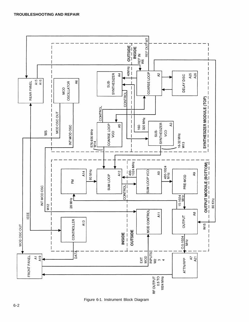
TROUBLESHOOTING AND REPAIR
Figure 6-1. Instrument Block Diagram
6-2
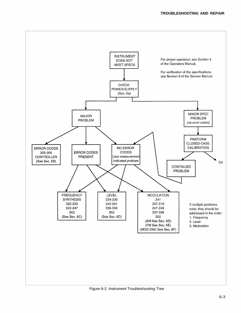
TROUBLESHOOTING AND REPAIR
6-3
Figure 6-2. Instrument Troubleshooting Tree
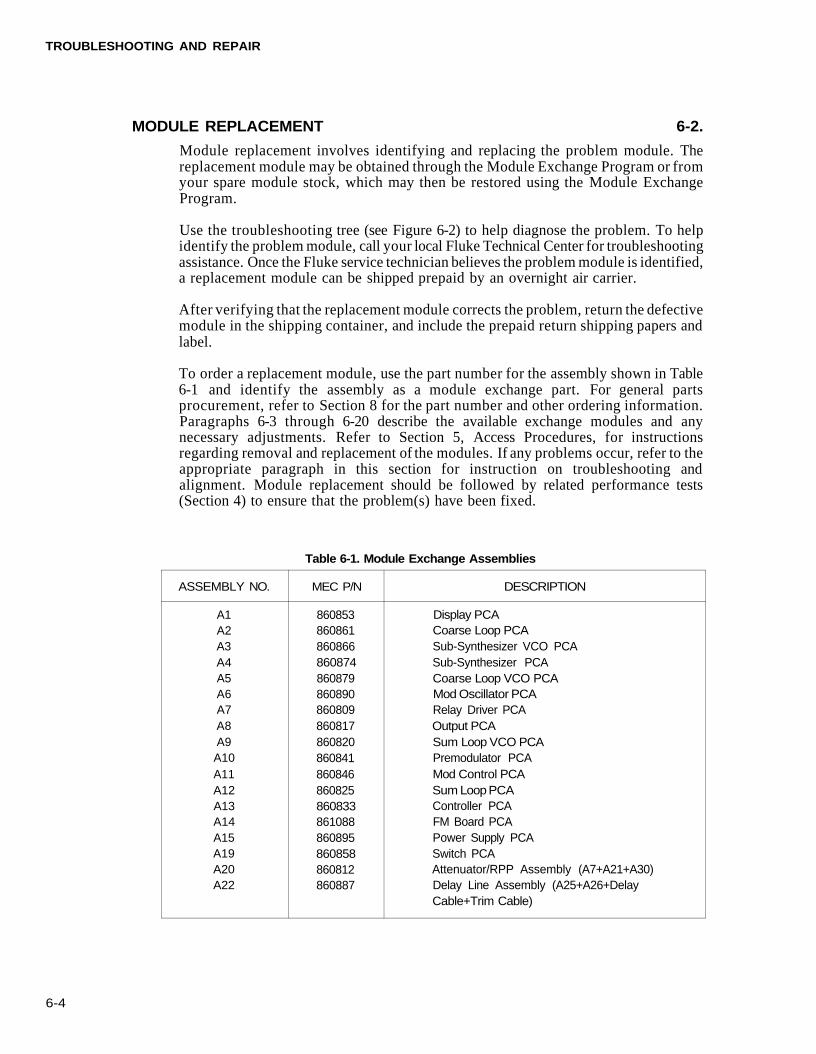
TROUBLESHOOTING AND REPAIR
MODULE REPLACEMENT 6-2.
Module replacement involves identifying and replacing the problem module. Thereplacement module may be obtained through the Module Exchange Program or fromyour spare module stock, which may then be restored using the Module ExchangeProgram.
Use the troubleshooting tree (see Figure 6-2) to help diagnose the problem. To helpidentify the problem module, call your local Fluke Technical Center for troubleshootingassistance. Once the Fluke service technician believes the problem module is identified,a replacement module can be shipped prepaid by an overnight air carrier.
After verifying that the replacement module corrects the problem, return the defectivemodule in the shipping container, and include the prepaid return shipping papers andlabel.
To order a replacement module, use the part number for the assembly shown in Table6-1 and identify the assembly as a module exchange part. For general partsprocurement, refer to Section 8 for the part number and other ordering information.Paragraphs 6-3 through 6-20 describe the available exchange modules and anynecessary adjustments. Refer to Section 5, Access Procedures, for instructionsregarding removal and replacement of the modules. If any problems occur, refer to theappropriate paragraph in this section for instruction on troubleshooting andalignment. Module replacement should be followed by related performance tests(Section 4) to ensure that the problem(s) have been fixed.
Table 6-1. Module Exchange Assemblies
ASSEMBLY NO.
A1A2A3A4A5A6A7A8A9A10A11A12A13A14A15A19A20A22
MEC P/N
860853860861860866860874860879860890860809860817860820860841860846860825860833861088860895860858860812860887
DESCRIPTION
Display PCACoarse Loop PCASub-Synthesizer VCO PCASub-Synthesizer PCACoarse Loop VCO PCAMod Oscillator PCARelay Driver PCAOutput PCASum Loop VCO PCAPremodulator PCAMod Control PCASum Loop PCAController PCAFM Board PCAPower Supply PCASwitch PCAAttenuator/RPP Assembly (A7+A21+A30)Delay Line Assembly (A25+A26+DelayCable+Trim Cable)
6-4
TROUBLESHOOTING AND REPAIR
A1 Display PCA 6-3.
Adjustments: None.
A2 Coarse Loop PCA 6-4.
Adjustments: None.
Perform Reference Oscillator Calibration. See paragraph 3-14.
A3 Sub-Synthesizer VCO PCA 6-5.
Adjustments: R106 on Sub-Synthesizer PCA. See paragraph 6C-9.
A compensation data EPROM containing VCO tuning data is included. Seeparagraph 6C-21 for data transfer instructions.
A4 Sub-Synthesizer PCA 6-6.
Adjustments: R106. See paragraph 6C-9.
Perform Reference Oscillator Calibration. See paragraph 3-14.
A5 Coarse Loop VCO PCA 6-7.
Adjustments: None.
Perform Coarse Loop compensation. See Appendix H.
A6 Mod Oscillator PCA 6-8.
Adjustments: None.
A7 Relay Driver PCA 6-9.
Adjustments: None.
A8 Output PCA 6-10.
Adjustments:
• R28, detector offset/linearity. See paragraph 6D-13 (Mod Control PCA).• R20, RF Level adjustment. See paragraph 6D-15 (Mod Control PCA).• RIO, AM Depth adjustment. See paragraph 6D-14 (Mod Control PCA).• R96, Q16 Bias adjustment. See paragraph 6D-21 (Output PCA).
A compensation data EPROM containing Output PCA level correction data isincluded. See paragraph 6-21 for data transfer instructions.
A9 Sum Loop VCO PCA 6-11.
Adjustments: R51 and C7, AM Bandwidth adjust. See paragraph 6D-20 (PremodulatorPCA).
Perform Sum Loop compensation. See Appendix H.
6-5
TROUBLESHOOTING AND REPAIR
A10 Premodulator PCA 6-12.
Adjustments: R51 and C7, AM Bandwidth adjust. See paragraph 6D-20.
A11 Modulation Control PCA 6-13.
Adjustments:
• R28, detector offset/linearity. See paragraph 6D-13.• R20, RF Level adjust. See paragraph 6D-15.• R10, AM Depth adjust. See paragraph 6D-14.
A12 Sum Loop PCA 6-14.
Adjustments: R116. See paragraph 6C-36.
A13 Controller PCA 6-15.
Adjustments: None.
To preserve the instrument calibration/compensation data, transfer the batterybacked RAM IC U8 and the EEPROM U9 from the old Controller PCA to thereplacement controller. If either U8 or U9 are bad, review "CALIBRATION/COMPENSATION MEMORY" (Section 6B) then replace the faulty IC.
A14 FM Board PCA 6-16.
Adjustments:
• R107, FM deviation high-rate. See paragraph 6E-18, item 12.• R39, HIDEV volts/steering. See paragraph 6E-20, item 8.• R35, LOWDEV volt/steering. See paragraph 6E-20, item 9.• R116 on Sum Loop PCA. See paragraph 6C-36.
A15 Power Supply PCA 6-17.
Adjustments: None..
A19 Switch PCA 6-18.
Adjustments: None.
A20 Attenuator/RPP Assembly (A7, A21, A30) 6-19.
Adjustments: R20, RF Level. See paragraph 6D-16 (Mod Control PCA).
A compensation data EPROM containing Attenuator/RPP level correction data isincluded. See paragraph 6-21 for data transfer instruction.
A22 Delay Line Assembly (A25, A26, Delay Cable, Trim Cable) 6-20.
Adjustments: None.
6-6
TROUBLESHOOTING AND REPAIR
UPDATING COMPENSATION MEMORY WITH MODULE EXCHANGE DATA 6-21.
After installing the A20 Attenuator/RPP, A8 Output, or A3 Sub-Synthesizer VCOmodule exchange assemblies, the operator must load the data in the correspondingcompensation EPROM into the compensation memory. The module exchangeEPROM is installed in a socket on the Al3 Controller PCA. The compensation data istransferred by one of three special functions, depending on which of the threeassemblies has been replaced.
Perform the following steps to update the compensation memory with the new moduleexchange data:
1. Verify that power to the 6080A/AN signal generator is turned off.
2. Access the A13 Controller PCA as described by the access procedure in Section 5.Leave the controller in place with all cables attached since it must be operational.
3. Install the module exchange EPROM into the socket on the controller labeledU10.
4. Power up the 6080A/AN.
5. Remove the sticker labeled "CAL|COMP" from the rear panel and set theCAL|COMP switch to the "1" position.
6. Verify that the CAL and COMP annunciators on the front panel are flashing.
7. Enter special function 961 to transfer the Attenuator/RPP data, special function962 to transfer the Output data, or special function 963 to transfer theSub-Synthesizer VCO data.
8 .Respond to the prompt "Att Sto?", "Out Sto?" or "Sub Sto ?" by pressing thekey.
The message "—Sto—" is displayed for 12 seconds for the attenuator, and 5seconds for the output and Sub-Synthesizer while the data is transferred.
CAUTION
Do not turn the POWER switch off or change the CAL|COMP switch until thestore operation is complete. Doing so could damage the contents of thecompensation memory.
9. Set the rear panel CAL|COMP switch to the "0" position.
10. Verify that the CAL and COMP annunciators are no longer flashing.
11. Turn the power off and remove the module exchange EPROM, if desired.
12. Reassemble the instrument by reversing the disassembly steps.
6-7
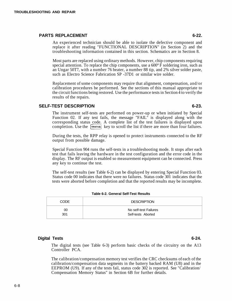
TROUBLESHOOTING AND REPAIR
PARTS REPLACEMENT 6-22.
An experienced technician should be able to isolate the defective component andreplace it after reading "FUNCTIONAL DESCRIPTION" (in Section 2) and thetroubleshooting information contained in this section. Schematics are in Section 8.
Most parts are replaced using ordinary methods. However, chip components requiringspecial attention. To replace the chip components, use a 600° F soldering iron, such asan Ungar 50T7, with a number 76 heater, a number 88 tip, and 2% silver solder paste,such as Electro Science Fabrication SP -37D1 or similar wire solder.
Replacement of some components may require that alignment, compensation, and/orcalibration procedures be performed. See the sections of this manual appropriate tothe circuit functions being restored. Use the performance tests in Section 4 to verify theresults of the repairs.
SELF-TEST DESCRIPTION 6-23.
The instrument self-tests are performed on power-up or when initiated by SpecialFunction 02. If any test fails, the message "FAIL" is displayed along with thecorresponding status code. A complete list of the test failures is displayed uponcompletion. Use the key to scroll the list if there are more than four failures.
During the tests, the RPP relay is opened to protect instruments connected to the RFoutput from possible damage.
Special Function 904 runs the self-tests in a troubleshooting mode. It stops after eachtest that fails leaving the hardware in the test configuration and the error code in thedisplay. The RF output is enabled so measurement equipment can be connected. Pressany key to continue the test.
The self-test results (see Table 6-2) can be displayed by entering Special Function 03.Status code 00 indicates that there were no failures. Status code 301 indicates that thetests were aborted before completion and that the reported results may be incomplete.
Table 6-2. General Self-Test Results
CODE
00301
DESCRIPTION
No self-test FailuresSelf-tests Aborted
Digital Tests 6-24.
The digital tests (see Table 6-3) perform basic checks of the circuitry on the A13Controller PCA.
The calibration/compensation memory test verifies the CRC checksums of each of thecalibration/compensation data segments in the battery backed RAM (U8) and in theEEPROM (U9). If any of the tests fail, status code 302 is reported. See "Calibration/Compensation Memory Status" in Section 6B for further details.
6-8
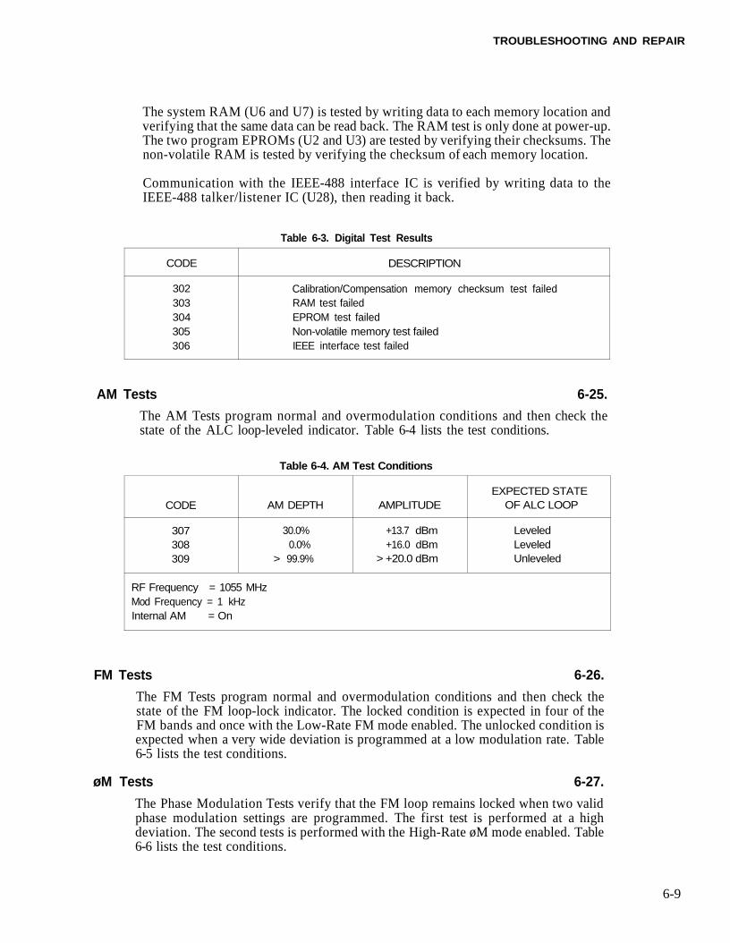
TROUBLESHOOTING AND REPAIR
The system RAM (U6 and U7) is tested by writing data to each memory location andverifying that the same data can be read back. The RAM test is only done at power-up.The two program EPROMs (U2 and U3) are tested by verifying their checksums. Thenon-volatile RAM is tested by verifying the checksum of each memory location.
Communication with the IEEE-488 interface IC is verified by writing data to theIEEE-488 talker/listener IC (U28), then reading it back.
Table 6-3. Digital Test Results
CODE
302303304305306
DESCRIPTION
Calibration/Compensation memory checksum test failedRAM test failedEPROM test failedNon-volatile memory test failedIEEE interface test failed
AM Tests 6-25.
The AM Tests program normal and overmodulation conditions and then check thestate of the ALC loop-leveled indicator. Table 6-4 lists the test conditions.
Table 6-4. AM Test Conditions
CODE
307308309
AM DEPTH
30.0%0.0%
> 99.9%
AMPLITUDE
+13.7 dBm+16.0 dBm
> +20.0 dBm
EXPECTED STATEOF ALC LOOP
LeveledLeveledUnleveled
RF Frequency = 1055 MHzMod Frequency = 1 kHzInternal AM = On
FM Tests 6-26.
The FM Tests program normal and overmodulation conditions and then check thestate of the FM loop-lock indicator. The locked condition is expected in four of theFM bands and once with the Low-Rate FM mode enabled. The unlocked condition isexpected when a very wide deviation is programmed at a low modulation rate. Table6-5 lists the test conditions.
øM Tests 6-27.
The Phase Modulation Tests verify that the FM loop remains locked when two validphase modulation settings are programmed. The first test is performed at a highdeviation. The second tests is performed with the High-Rate øM mode enabled. Table6-6 lists the test conditions.
6-9
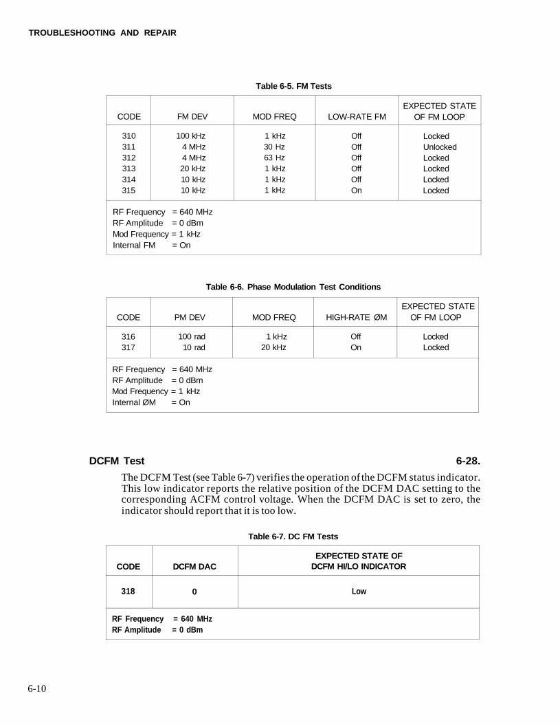
TROUBLESHOOTING AND REPAIR
Table 6-5. FM Tests
Table 6-6. Phase Modulation Test Conditions
DCFM Test 6-28.
The DCFM Test (see Table 6-7) verifies the operation of the DCFM status indicator.This low indicator reports the relative position of the DCFM DAC setting to thecorresponding ACFM control voltage. When the DCFM DAC is set to zero, theindicator should report that it is too low.
Table 6-7. DC FM Tests
6-10
CODE
310311312313314315
FM DEV
100 kHz4 MHz4 MHz20 kHz10 kHz10 kHz
MOD FREQ
1 kHz30 Hz63 Hz1 kHz1 kHz1 kHz
LOW-RATE FM
OffOffOffOffOffOn
EXPECTED STATEOF FM LOOP
LockedUnlockedLockedLockedLockedLocked
RF Frequency = 640 MHzRF Amplitude = 0 dBmMod Frequency = 1 kHzInternal FM = On
CODE
316317
PM DEV
100 rad10 rad
MOD FREQ
1 kHz20 kHz
HIGH-RATE ØM
OffOn
EXPECTED STATEOF FM LOOP
LockedLocked
RF Frequency = 640 MHzRF Amplitude = 0 dBmMod Frequency = 1 kHzInternal ØM = On
CODE
318
DCFM DAC
0
EXPECTED STATE OFDCFM HI/LO INDICATOR
Low
RF Frequency = 640 MHzRF Amplitude = 0 dBm
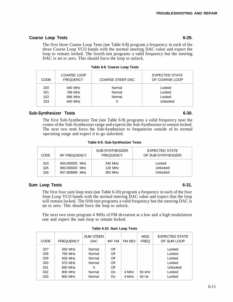
TROUBLESHOOTING AND REPAIR
Coarse Loop Tests 6-29.
The first three Coarse Loop Tests (see Table 6-8) program a frequency in each of thethree Coarse Loop VCO bands with the normal steering DAC value and expect theloop to remain locked. The fourth test programs a valid frequency but the steeringDAC is set to zero. This should force the loop to unlock.
Table 6-8. Coarse Loop Tests
Sub-Synthesizer Tests 6-30.
The first Sub-Synthesizer Test (see Table 6-9) programs a valid frequency near thecenter of the Sub-Synthesizer range and expects the Sub-Synthesizer to remain locked.The next two tests force the Sub-Synthesizer to frequencies outside of its normaloperating range and expect it to go unlocked.
Table 6-9. Sub-Synthesizer Tests
Sum Loop Tests 6-31.
The first four sum loop tests (see Table 6-10) program a frequency in each of the fourSum Loop VCO bands with the normal steering DAC value and expect that the loopwill remain locked. The fifth test programs a valid frequency but the steering DAC isset to zero. This should force the loop to unlock.
The next two tests program 4 MHz of FM deviation at a low and a high modulationrate and expect the sum loop to remain locked.
Table 6-10. Sum Loop Tests
6-11
CODE
320321322323
COARSE LOOPFREQUENCY
640 MHz768 MHz896 MHz640 MHz
COARSE STEER DAC
NormalNormalNormal
0
EXPECTED STATEOF COARSE LOOP
LockedLockedLockedUnlocked
CODE
324325326
RF FREQUENCY
804.000000 MHz800.000000 MHz807.999999 MHz
SUB-SYNTHESIZERFREQUENCY
240 MHz120 MHz350 MHz
EXPECTED STATEOF SUB-SYNTHESIZER
LockedUnlockedUnlocked
CODE
327328329330331332333
FREQUENCY
550 MHz700 MHz830 MHz975 MHz550 MHz800 MHz800 MHz
SUM STEERDAC
NormalNormalNormalNormal
0NormalNormal
INT FM
OffOffOffOffOffOnOn
FM DEV
4 MHz4 MHz
MODFREQ
50 kHz63 Hz
EXPECTED STATEOF SUM LOOP
LockedLockedLockedLockedUnlockedLockedLocked
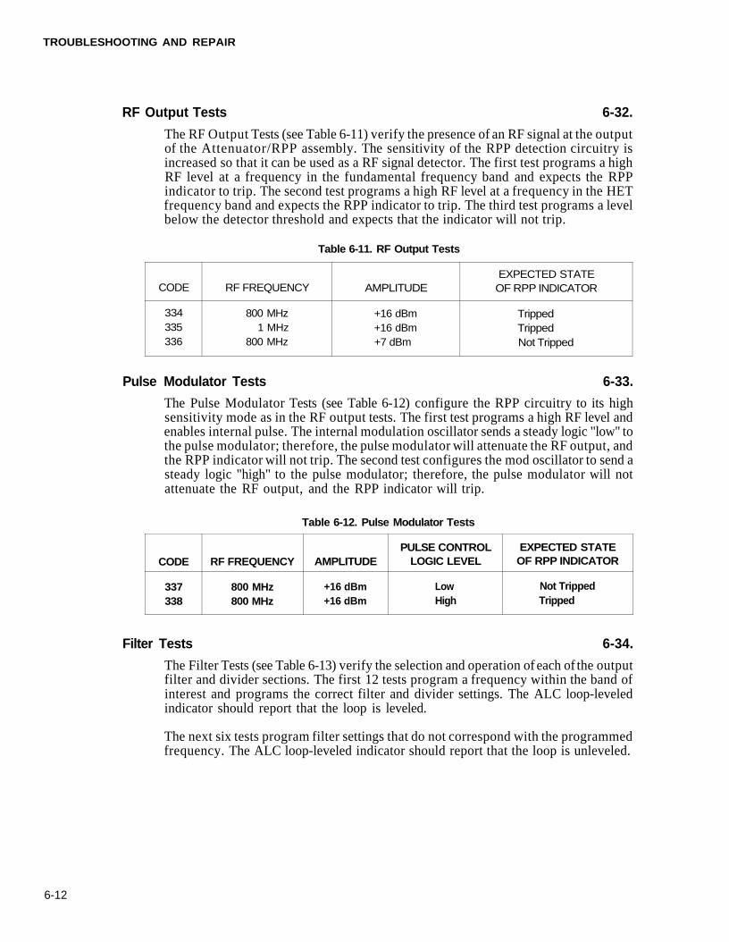
TROUBLESHOOTING AND REPAIR
RF Output Tests 6-32.
The RF Output Tests (see Table 6-11) verify the presence of an RF signal at the outputof the Attenuator/RPP assembly. The sensitivity of the RPP detection circuitry isincreased so that it can be used as a RF signal detector. The first test programs a highRF level at a frequency in the fundamental frequency band and expects the RPPindicator to trip. The second test programs a high RF level at a frequency in the HETfrequency band and expects the RPP indicator to trip. The third test programs a levelbelow the detector threshold and expects that the indicator will not trip.
Table 6-11. RF Output Tests
Pulse Modulator Tests 6-33.
The Pulse Modulator Tests (see Table 6-12) configure the RPP circuitry to its highsensitivity mode as in the RF output tests. The first test programs a high RF level andenables internal pulse. The internal modulation oscillator sends a steady logic "low" tothe pulse modulator; therefore, the pulse modulator will attenuate the RF output, andthe RPP indicator will not trip. The second test configures the mod oscillator to send asteady logic "high" to the pulse modulator; therefore, the pulse modulator will notattenuate the RF output, and the RPP indicator will trip.
Table 6-12. Pulse Modulator Tests
Filter Tests 6-34.
The Filter Tests (see Table 6-13) verify the selection and operation of each of the outputfilter and divider sections. The first 12 tests program a frequency within the band ofinterest and programs the correct filter and divider settings. The ALC loop-leveledindicator should report that the loop is leveled.
The next six tests program filter settings that do not correspond with the programmedfrequency. The ALC loop-leveled indicator should report that the loop is unleveled.
6-12
CODE
334335336
RF FREQUENCY
800 MHz1 MHz
800 MHz
AMPLITUDE
+16 dBm+16 dBm+7 dBm
EXPECTED STATEOF RPP INDICATOR
TrippedTrippedNot Tripped
CODE
337338
RF FREQUENCY
800 MHz800 MHz
AMPLITUDE
+16 dBm+16 dBm
PULSE CONTROLLOGIC LEVEL
LowHigh
EXPECTED STATEOF RPP INDICATOR
Not TrippedTripped
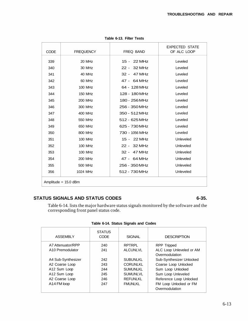
TROUBLESHOOTING AND REPAIR
Table 6-13. Filter Tests
STATUS SIGNALS AND STATUS CODES 6-35.
Table 6-14. lists the major hardware status signals monitored by the software and thecorresponding front panel status code.
Table 6-14. Status Signals and Codes
6-13
CODE
339
340
341
342
343
344
345
346
347
348
349
350
351
352
353
354
355
356
FREQUENCY
20 MHz
30 MHz
40 MHz
60 MHz
100 MHz
150 MHz
200 MHz
300 MHz
400 MHz
550 MHz
650 MHz
800 MHz
100 MHz
100 MHz
100 MHz
200 MHz
500 MHz
1024 MHz
FREQ BAND
15 - 22 MHz
22 - 32 MHz
32 - 47 MHz
47 - 64 MHz
64 - 128 MHz
128 - 180 MHz
180 - 256 MHz
256 - 350 MHz
350 - 512 MHz
512 - 625 MHz
625 - 730 MHz
730 - 1056 MHz
15 - 22 MHz
22 - 32 MHz
32 - 47 MHz
47 - 64 MHz
256 - 350 MHz
512 - 730 MHz
EXPECTED STATEOF ALC LOOP
Leveled
Leveled
Leveled
Leveled
Leveled
Leveled
Leveled
Leveled
Leveled
Leveled
Leveled
Leveled
Unleveled
Unleveled
Unleveled
Unleveled
Unleveled
Unleveled
Amplitude = 15.0 dBm
ASSEMBLY
A7 Attenuator/RPPA10 Premodulator
A4 Sub-SynthesizerA2 Coarse LoopA12 Sum LoopA12 Sum LoopA2 Coarse LoopA14 FM loop
STATUSCODE
240241
242243244245246247
SIGNAL
RPTRPLALCUNLVL
SUBUNLKLCORUNLKLSUMUNLKLSUMUNLVLREFUNLKLFMUNLKL
DESCRIPTION
RPP TrippedALC Loop Unleveled or AMOvermodulationSub-Synthesizer UnlockedCoarse Loop UnlockedSum Loop UnlockedSum Loop UnleveledReference Loop UnlockedFM Loop Unlocked or FMOvermodulation
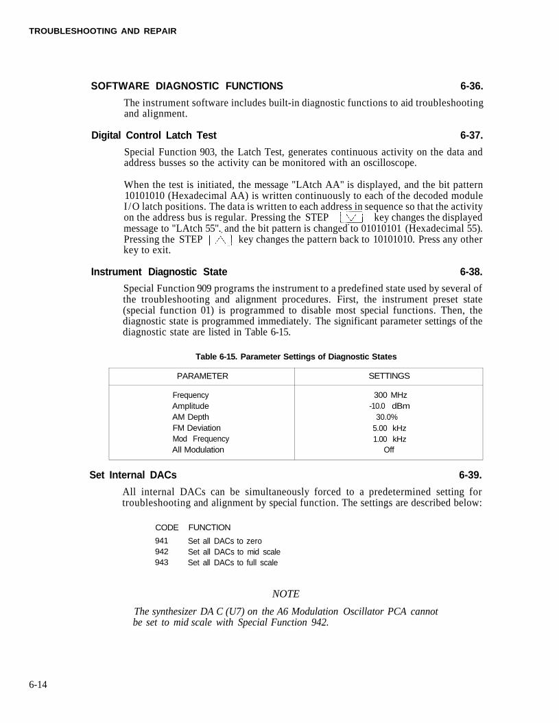
TROUBLESHOOTING AND REPAIR
SOFTWARE DIAGNOSTIC FUNCTIONS 6-36.
The instrument software includes built-in diagnostic functions to aid troubleshootingand alignment.
Digital Control Latch Test 6-37.
Special Function 903, the Latch Test, generates continuous activity on the data andaddress busses so the activity can be monitored with an oscilloscope.
When the test is initiated, the message "LAtch AA" is displayed, and the bit pattern10101010 (Hexadecimal AA) is written continuously to each of the decoded moduleI /O latch positions. The data is written to each address in sequence so that the activityon the address bus is regular. Pressing the STEP key changes the displayedmessage to "LAtch 55", and the bit pattern is changed to 01010101 (Hexadecimal 55).Pressing the STEP key changes the pattern back to 10101010. Press any otherkey to exit.
Instrument Diagnostic State 6-38.
Special Function 909 programs the instrument to a predefined state used by several ofthe troubleshooting and alignment procedures. First, the instrument preset state(special function 01) is programmed to disable most special functions. Then, thediagnostic state is programmed immediately. The significant parameter settings of thediagnostic state are listed in Table 6-15.
Table 6-15. Parameter Settings of Diagnostic States
Set Internal DACs 6-39.
All internal DACs can be simultaneously forced to a predetermined setting fortroubleshooting and alignment by special function. The settings are described below:
CODE
941942943
FUNCTION
Set all DACs to zeroSet all DACs to mid scaleSet all DACs to full scale
NOTE
The synthesizer DA C (U7) on the A6 Modulation Oscillator PCA cannotbe set to mid scale with Special Function 942.
6-14
PARAMETER
FrequencyAmplitudeAM DepthFM DeviationMod FrequencyAll Modulation
SETTINGS
300 MHz-10.0 dBm
30.0%5.00 kHz1.00 kHz
Off
TROUBLESHOOTING AND REPAIR
Display Synthesizer Loop Frequencies 6-40.
The sum loop, coarse loop, and sub-synthesizer frequencies for the programmed RFoutput frequency can be displayed by the Special Functions listed below:
6-15/6-16
CODE
945946947
FUNCTION
Display Sum Loop frequencyDisplay Coarse Loop frequencyDisplay Sub-Synthesizer frequency

Section 6APower Supply
POWER SUPPLY BLOCK DIAGRAM 6A-1.
Refer to the Power Supply Block Diagram, Figure 6A-1, to identify the majorfunctional sections and for help in following the power and current paths of the powersupply.
POWER SUPPLY CIRCUIT DESCRIPTION 6A-2.
The instrument power supply provides all the DC and AC power requirements of thesystem. The DC supplies are provided to all circuitry of the system and to the DC fan.The AC power is used for filament heat for the front panel display.
Line power passes through the line filter and fuse. The filter also provides switching forthe various power line voltages, from which the instrument is designed to operate. TheAC power is then routed to the power transformer primary winding. The transformerincludes an additional safety device, which serves as a thermal shutoff to break theprimary AC supply in case the transformer exceeds a safe operating temperature.
To accommodate the various line voltages, the case of the line fused receptacle/filter ofthe 6080A/AN contains a line voltage selector card that can be plugged in two differentways. Plugging the line voltage selector card into one of its two positions allowsselecting the line voltage of 115 or 230V AC.
The secondary windings of the transformer are connected to a linear DC power supplyassembly that provides the instrument with the supplies shown in Table 6A-1.
NOTE
The front panel power switch does not break the AC line power or thetransformer secondary. The power supply and some other parts of theinstrument, such as the display assembly, are powered while the line plugis energized.
In the standby mode (power switch is off) the active supplies are the 23.4V and thedisplay filament lines. In addition, various parts of the power supply assembly areenergized, such as all transformer secondary windings, rectifiers, and filter capacitors.
The bridge rectifiers in the power supply are used in either a bridge or full-wavecenter-tapped configuration with capacitor input filters. Figure 6A-1 shows therectifier configurations as well as the component designations for the various supplies.
6A-1
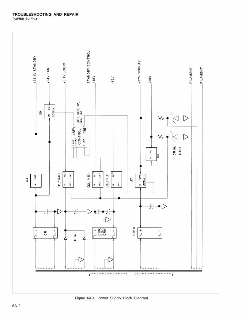
TROUBLESHOOTING AND REPAIRPOWER SUPPLY
Figure 6A-1. Power Supply Block Diagram
6A-2
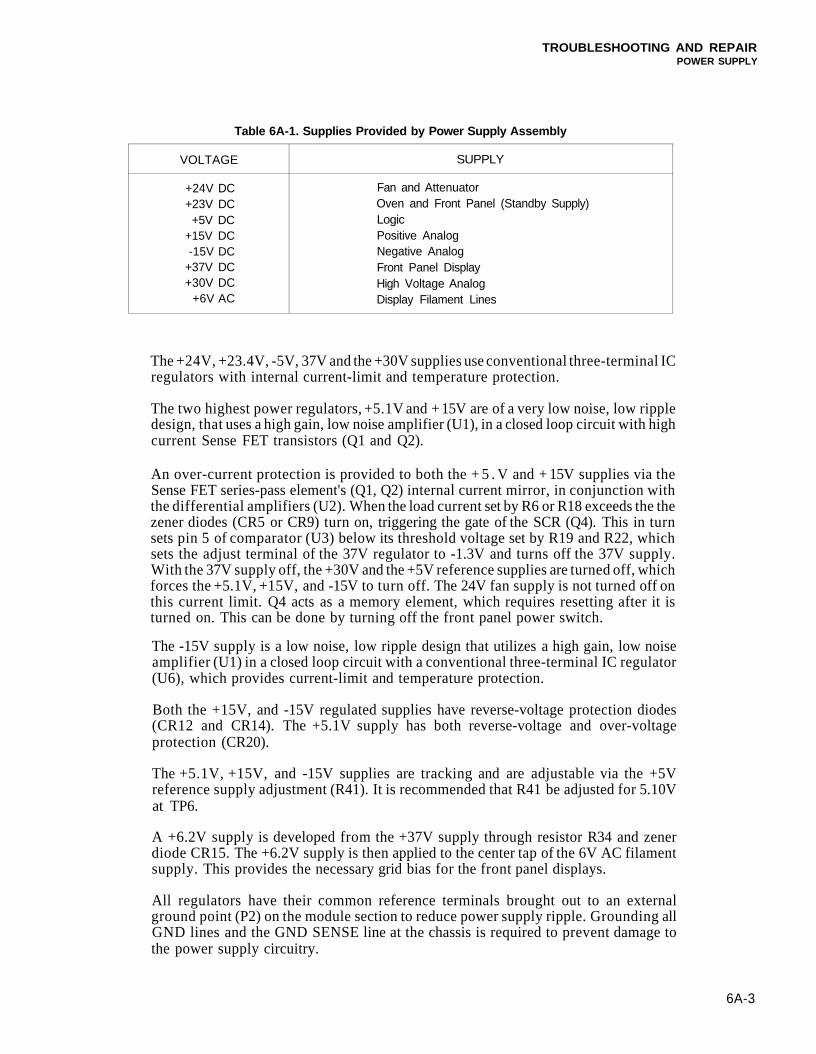
TROUBLESHOOTING AND REPAIRPOWER SUPPLY
Table 6A-1. Supplies Provided by Power Supply Assembly
VOLTAGE
+24V DC+23V DC+5V DC
+15V DC-15V DC
+37V DC+30V DC
+6V AC
SUPPLY
Fan and AttenuatorOven and Front Panel (Standby Supply)LogicPositive AnalogNegative AnalogFront Panel DisplayHigh Voltage AnalogDisplay Filament Lines
The +24V, +23.4V, -5V, 37V and the +30V supplies use conventional three-terminal ICregulators with internal current-limit and temperature protection.
The two highest power regulators, +5.1V and + 15V are of a very low noise, low rippledesign, that uses a high gain, low noise amplifier (U1), in a closed loop circuit with highcurrent Sense FET transistors (Q1 and Q2).
An over-current protection is provided to both the + 5 . V and + 15V supplies via theSense FET series-pass element's (Q1, Q2) internal current mirror, in conjunction withthe differential amplifiers (U2). When the load current set by R6 or R18 exceeds the thezener diodes (CR5 or CR9) turn on, triggering the gate of the SCR (Q4). This in turnsets pin 5 of comparator (U3) below its threshold voltage set by R19 and R22, whichsets the adjust terminal of the 37V regulator to -1.3V and turns off the 37V supply.With the 37V supply off, the +30V and the +5V reference supplies are turned off, whichforces the +5.1V, +15V, and -15V to turn off. The 24V fan supply is not turned off onthis current limit. Q4 acts as a memory element, which requires resetting after it isturned on. This can be done by turning off the front panel power switch.
The -15V supply is a low noise, low ripple design that utilizes a high gain, low noiseamplifier (U1) in a closed loop circuit with a conventional three-terminal IC regulator(U6), which provides current-limit and temperature protection.
Both the +15V, and -15V regulated supplies have reverse-voltage protection diodes(CR12 and CR14). The +5.1V supply has both reverse-voltage and over-voltageprotection (CR20).
The +5.1V, +15V, and -15V supplies are tracking and are adjustable via the +5Vreference supply adjustment (R41). It is recommended that R41 be adjusted for 5.10Vat TP6.
A +6.2V supply is developed from the +37V supply through resistor R34 and zenerdiode CR15. The +6.2V supply is then applied to the center tap of the 6V AC filamentsupply. This provides the necessary grid bias for the front panel displays.
All regulators have their common reference terminals brought out to an externalground point (P2) on the module section to reduce power supply ripple. Grounding allGND lines and the GND SENSE line at the chassis is required to prevent damage tothe power supply circuitry.
6A-3
TROUBLESHOOTING AND REPAIRPOWER SUPPLY
The -5V local supply (U5) provides negative voltage to U1 and a -1.3V for U7 and U9shut off voltage, U3. Triac Q3 is a voltage surge protector to protect against line voltagesurges as well as overvoltage in case of a wrong setting of the line power selector card.When the voltage across the +5.1V secondary winding of the transformer is excessive,CR2 or CR3 conduct current which fires the gate of Q3. This sets Q3 in the conductivemode, shorting the secondary winding and causing the power line fuse to blow.
POWER SUPPLY TROUBLESHOOTING 6A-3.
WARNING
TROUBLESHOOTING THE POWER SUPPLY SHOULD BE DONE WITHGREAT CAUTION SINCE IT IS POWERED UP WHILE THE LINE POWER ISCONNECTED TO THE INSTRUMENT. THE FRONT PANEL POWER SWITCHDOES NOT BREAK EITHER THE AC LINE POWER OR THE TRANS-FORMER SECONDARY. THEREFORE, THE POWER SUPPLY ISENERGIZED WHENEVER IT IS CONNECTED TO THE MAINS.
To troubleshoot the power supply, remove the rear panel from the instrument andremove the Power Supply PCA from its bracket.
Since the power supply is a floating type (to reduce ground loops) both the GND linesand the GND SENSE lines must be connected via the controller connector (J4). It is agood practice to connect load resistors to each of the supply lines. The load valuesshould correspond to the load current indicated on the power supply schematic.
When operating the power supply, make sure that the fan is aimed at the powerdissipators (Q1, Q2, U6, U4, U9). Failure to provide adequate air flow could damagethe power supply.
Troubleshooting Procedure 6A-4.
Troubleshoot the power supply as described in the following procedure:
1. Set the power supply to the standby mode (front panel yellow LED on).
2. Verify that the two standby supplies are operating and are within the specifiedvoltage range, and verify that the rest of the supplies are turned off. The specifiedranges are as follows:
a. TP2, 23.4V supply = 24V (± 5%)b. TP14, -5Vsupply = -5V (±5%)c. TP18, 24V supply = 0V (±0.1V)d. TP6, +5.1V supply = 0V (±0.1V)e. TP11, + 15V supply = 0V (± 0.1V)f. TP16, -15V supply = 0V (± 0.1V)g. TP20, 37V supply = 0V (± 0.1V)h. TP21, 30V supply = 0V (± 0.1V)i. TP15, +5V reference = 0V (± 0.1V)
6A-4
TROUBLESHOOTING AND REPAIRPOWER SUPPLY
3. If either of the 23.4V or -5V supplies are not at the specified voltage, check theunregulated supply for both (TP13 and TP1, respectively).
If some of the supplies that are supposed to be off are partially or fully turned on,check the 37V supply (TP20) voltage.
If the 37V supply is partially or fully on, check the standby switching circuit and thecomparator operation (U3, Q5, R52).
4. Next, switch the power supply on, by connecting the STANDBY line pin to GND(J6 pin 7,8).
5. Verify all supplies are operating and are within the following specified levels:
a. TP18, 24V supply = 24V (± 5%)b. TP2, 23.4V supply = 24V (± 5%)c. TP6, +5.1V supply = 5.1V (± 2%)d. TP11,+15V supply = 15V (± 4%)e. TP16, -15V supply = -15V (± 4 %)f. TP14, -5V supply = -5V (± 5%)g. TP20, 37V supply = 37V (± 5%)h. TP21, 30Vsupply = 30V (± 5%)i. TP15, +5V reference = 5V (± 3%)
6. If all supplies are at the appropriate voltages when in standby, but are not at theappropriate voltages when the power supply is on, verify that the all standbysupplies are correct.
If the fan supply (24V) is on and the rest of the supplies (with the exception of the23.4 and -5V) are off, check the current limit circuitry (U2, CR5, CR9, Q4). A shortat either the +15 or the +5.1 could cause the current limit to trip and turn allnon-standby supplies off, with the exception of the fan supply. In this case, verifythat the voltage at TP22 is less than 1V, which indicates a current-limit trip. Torecover from a current limit shutoff, turn off the power supply (to standbyoperation) for at least 5 seconds.
7. If only the +5 V reference, +5.1V, +15V, and the -15V supplies are in error, check the+5V reference circuitry, since it is likely that the fault is with the reference supply,U1, CR16.
POWER SUPPLY ADJUSTMENT PROCEDURE 6A-5.
A single adjustment potentiometer is provided for adjusting the voltage output of thethree discrete supplies: the +5.1, +15, and -15V. To adjust these supplies, place avoltmeter at the +5.1V supply (TP6) and adjust R41 for 5.1V (± 0.05V). Since the+5.1V, +15V, and 15V supplies are of tracking design, both the +15 and the -15Vsupplies should be at 15V ± 0.2V.
6A-5/6A-6

Section 6BDigital Controller
DIGITAL CONTROLLER BLOCK DIAGRAM 6B-1.
The A13 Controller PCA, under the direction of the instrument software, handles thedata interface between the front panel, remote interface, and 6080A/AN functions.The controller is located in a top side compartment of the lower module section.
The controller consists of the following functional groups:
MicroprocessorMemoryFront Panel InterfaceIEEE-488 InterfaceAttenuator Control InterfaceModule I/O InterfaceStatus and Control Latches
Refer to Figure 6B-1 to identify the major sections and trace signal paths.
DIGITAL CONTROLLER CIRCUIT DESCRIPTION (A13) 6B-2.
Microprocessor 6B-3.
The software is executed on a 68HCOOO 16-bit microprocessor. The 8-MHz digitalsystem clock signal is generated by an oscillator comprised of gates from U18 andcrystal Yl.
Supply voltage monitor TL7705A (U13) generates the active low reset signal to the68HC000. The reset signal is generated on power-up or if the +5V supply drops below+4.5V. The reset signal remains low for 200 ms.
Memory 6B-4.
The program instructions and constant data are stored in two 128-KB EPROMs, U2and U3. The stack and program variables are stored in two 8-KB static RAMs U6 andU7. Non-volatile front panel setups, and one half of the redundant calibration/compensation memory are contained in the battery-backed CMOS RAM U8. Theother half of the redundant calibration/compensation memory is contained in theEEPROM U9.
The rear panel CAL|COMP switch protects the calibration/compensation memoryfrom accidental destruction.
6B-1
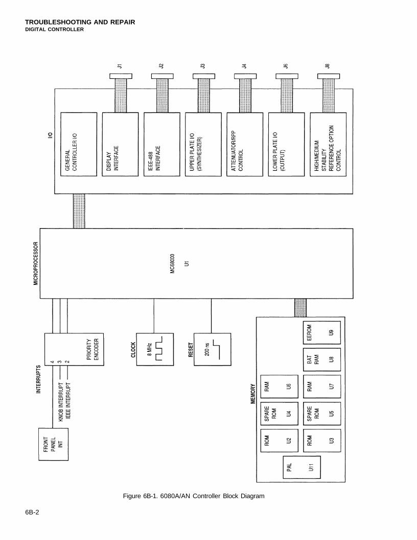
TROUBLESHOOTING AND REPAIRDIGITAL CONTROLLER
6B-2
Figure 6B-1. 6080A/AN Controller Block Diagram
TROUBLESHOOTING AND REPAIRDIGITAL CONTROLLER
Memory Control 6B-5.
Decoder PAL U11 decodes the memory selects and contains additional writeprotection logic for the the calibration/compensation memory and the instrumentstates stored in the battery-backed RAM. Timing PAL U15 adds one wait state to eachmemory read or write cycle.
Individual upper-byte and lower-byte read and write enable signals are generated from68HCOOO control signals R / W , UDS, and LDS by U22. Signals RDU and RDL areread enables for the upper-byte and lower-byte respectively. Signals WRU and WRLare write enables for the upper-byte and lower-byte respectively.
Front Panel Interface 6B-6.
Data is transferred to and from the front panel circuitry through tri-state bidirectionaldata buffer U31. The corresponding address signals are transferred through tri-statebuffer U32. These buffers are active when a front panel latch is addressed and thebuffer control signal from U43 is low. Otherwise, the buffer is in the high-impedancestate. To reduce RF emissions from the Generator, low-pass filters and bypasscapacitors are used on all data and select signals to the front panel.
The front panel interrupt rate is determined by the binary dividers U14 and U20. Undernormal operation, the system clock is divided by 8192 to generate a front panelinterrupt every 540 microseconds. When the display is blanked by special function, theinterrupt rate is divided by an additional factor of 32 to reduce the burden on themicroprocessor, thus reducing the software response time.
IEEE-488 Interface 6B-7.
All IEEE-488 communications are handled by U28, an NEC μPD7210 talker/listenerIC. The 7210 is connected directly to the system address and data bus andcommunicates with the microprocessor as a memory mapped I/O device.
The active low interrupt signal IEINTL is connected to the level two interrupt on themicroprocessor. Tri-state bus drivers U29 and U30 interface the 7210 directly to theIEEE-488 bus.
Attenuator Control Interface 6B-8.
The attenuator control signals are latched by U39. Darlington driver U40 provides thelevel shifting necessary to control the A7 Relay Driver/RPP PCA.
Module I/O 6B-9.
Control data is transferred to the RF circuitry through two byte-wide unidirectionaldata buses. Data is transferred to the upper module through J3 and to the lowermodule through J6.
Select lines BSEL0L, BSEL1L, and BSEL5L, and address lines SAB2, SAB1, andSAB0 are decoded into individual latch enables for the upper module on the A4subsynthesizer PCA. Tri-state buffers U24 and U33 provide drive current when activeand allow these signals to float when inactive.
Select lines BSEL2L, BSEL3L, and BSEL4L and address lines BAB2, BAB1, andBAB0 are decoded into individual latch enables for the lower module on the A11Modulation Control PCA. Tri-state buffers U25 and U27 provide drive current whenactive and allow these signals to float when inactive.
6B-3
TROUBLESHOOTING AND REPAIRDIGITAL CONTROLLER
Timing PAL U15 adds additional wait states to each module I/O write cycle to ensurethat adequate setup and hold times are provided for every IC on the bus.
Status and Control 6B-10.
Input buffers U35, U36, U37, and U45 read the fault detector signals, hardware statussignals, the option status signals, and the status of the REF INT/EXT andCAL|COMP switches. Control and buffer enable data is latched by output latchesU34 and U38.
DIGITAL CONTROLLER TROUBLESHOOTING 6B-11.
If the symptoms indicate a digital or control problem, the following suggestions mayhelp isolate the fault to a particular functional circuit. Refer to the schematic diagramsin Section 8.
Verify that all assemblies are receiving the correct voltages from the power supply.
The most obvious symptom of failure in the A13 Controller PCA is a blank frontpanel. A properly operating front panel indicates that most of the controller anddisplay circuitry is functional. If the front panel is totally blank or unresponsive tokeystrokes, make sure that the display blanking special function is not active bypressing the key or by cycling the power. If the front panel is still blank, referto "Microprocessor Kernel" later in Section 6B.
If the front panel is operating correctly but the RF output is incorrect, try to determineif the fault is on the controller or on an RF circuit board by programming variousfunctions and checking for status codes.
RF Control 6B-12.
Communication with the RF circuitry in the upper and lower modules is throughconnectors J3 and J6 respectively. The RF data and control signals to both modulesare buffered by tri-state drivers that are active only while data is being transferred andare in the high-impedance state at all other times.
Special Function 903, the latch test, generates continuous activity on the data andaddress buses so that the activity can be monitored with an oscilloscope. The latch testis described under "SOFTWARE DIAGNOSTIC FUNCTIONS" in Section 6.
Enter Special Function 903 to initiate the latch test. Use an oscilloscope to inspect thechip select signals at the inputs and at the outputs of buffers U24 and U25. The firstsymptom to look for is totally inactive signals or invalid logic states. If there are no chipselect signals present at the inputs of U23, refer to "Address Decoding" later in Section6B.
If all of the chip select signals are operating correctly, connect a scope probe to thesignal BSEL0L and use the high-to-low transition of the signal to trigger the scope. Useanother probe to inspect the data and address signals buffered by U24, U25, U27, andU33 during the low period of BSEL0L. Look for inactive signals and invalid logicstates. Also compare the buffer inputs to their outputs. Press the STEP key,then the STEP key to toggle each of the data signals. In addition, make surethat the buffer control signals are low (active).
6B-4
TROUBLESHOOTING AND REPAIRDIGITAL CONTROLLER
If the signals pass the above tests, check the data and address signals at any suspiciouslatch or DAC on the suspect RF circuit board. If a DAC problem is suspected, usespecial functions 941, 942, and 943, which set all DACs to zero, half scale, and full scalerespectively.
Microprocessor Kernel 6B-13.
A blank front panel is a symptom of many controller-related problems. Micropro-cessor-related problems are difficult to troubleshoot because of the volume of activityat any given time. However, one can systematically verify the independent circuitfunctions and quickly spot some of the most obvious problems. Read the followingparagraphs and verify the related circuitry.
Clock 6B-14.
Connect an oscilloscope probe to the clock oscillator output (U18 pin 4). There shouldbe a symmetrical 8-MHz square wave with adequate logic levels. If the signal appearsabnormal, determine if the problem is with the oscillator circuit or the ICs connected tothe clock output by checking the input signal at pin 3 of U18. It should be an invertedversion of the same 8-MHz square wave. (It may be slightly distorted due to itsloading.)
Power-On Reset 6B-15.
Connect an oscilloscope probe to the RESET input (pin 18) of U1. The signal shouldgenerate a low to high transition on power-up and remain high during normaloperation. Turning the power off and on generates an active low reset pulseapproximately 200 ms wide.
If the reset pulse to U1 appears abnormal, compare it to the reset output (pin 5) of thepower supply monitor IC U13. Suspect problems with U13, and all ICs connected tothe RESETL and RESETH signals.
Also check the HALT input (pin 17) of U1; it should look like the RESET (pin 18)input.
Unused Microprocessor Inputs 6B-16.
Input signals to U1, BR (pin 13) and BGACK (pin 12) should both be high. If either ofthese signals is not high, correct the fault before continuing.
Bus Error 6B-17.
The bus error input BERR (pin 22) notifies the microprocessor when a memory cyclecannot be completed as a result of a hardware fault. Normally, the BERR signal shouldalways remain high.
If the BERR signal goes low, verify that pin 1 of U14 is clocked by an 800-kHz signalwith a 60/40 duty cycle. Also verify that pin 2 of U14 is receiving continuous activityfrom the address strobe signal (AS).
Interrupts 6B-18.
The front panel edit knob interrupt is generated on the A1 Display PCA when the knobis turned. The interrupt signal from the display PCA connects to U12 pin 13. If it is lowwhen the knob is in the rest position, refer to "Edit Knob Interface" later in Section 6B.
6B-5
TROUBLESHOOTING AND REPAIRDIGITAL CONTROLLER
Under normal operation, a front panel interrupt should be generated every 540 μs atpin 6 of U21. If the display has been turned off by special function, there should be aninterrupt generated every 16.3 ms. Verify the divided outputs from U14 and U20 andmake sure that a reset signal at U21 pin 1 is generated after each interrupt.
Verify that the IEEE-488 Interface interrupt signal, IEINTL, is in the inactive (high)state. If IEINTL is active, make sure the microprocessor kernel and buses areoperating correctly since the software must be operating before the IEEE interrupt canbe initialized properly. Next, troubleshoot communications with the IEEE-488interface IC using the diagnostic tests under the heading "I/O Diagnostic Tests" later inSection 6B.
Microprocessor Bus 6B-19.
The dynamic nature of the microprocessor bus makes it difficult to verify the datatransmitted at any given time. However, most common bus faults show recognizablesymptoms and can be found with the aid of the address bus diagnostic test.
To initiate the bus diagnostic test, turn off the instrument power and set DIP switches2, 3, and 4 of S1 to the on position. Remove U11 from its socket to disable all memoryand I/O chip selects, then turn the power on. This test generates predictable activity onthe control signals and the address bus.
Look at the bus control signals (AS, R/W, UDS, LDS) with an oscilloscope. Suspectinactive signals or signals that enter invalid logic states. Also compare the inputs andoutputs of gated signals.
All the address bus signals should have square waves of varying frequencies. Theleast-significant signal (A1) has the highest frequency, and successively higher ordersignals have a frequency half that of the previous line. Note that there are small glitcheson all of the address signals during the low cycle. These are normal and are not reallyglitches. The address lines are momentarily tri-stated between bus cycles, and thepull-up resistors only pull the signals part way up before the next bus cycle begins.
If the microprocessor bus test does not function as described, suspect the micro-processor kernel and the data bus. Check for data lines shorted together or shorted tothe power supply. Also look for ICs that may be driving the data bus
If the control and address signals appear normal, set the DIP switches to the offposition and install U11.
Address Decoder 6B-20.
Several levels of address decoding are used to select the memory and I/O devices.Figure 6B-2 shows the levels of decoding.
Decoder PAL U11 generates the major memory segment selects. Verify that all of itsaddress and control inputs are working properly. The signal CMWRL is thewrite-protection signal for the calibration/compensation memory. Signal CMWRL istied directly to the rear panel CAL|COMP switch. Signals NVWR and COMPWR aresoftware controlled write-protection signals for the non-volatile memory and thecalibration/compensation memory, respectively.
6B-6
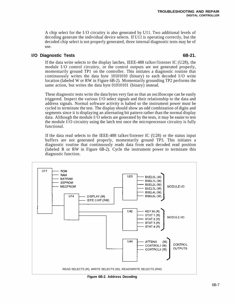
TROUBLESHOOTING AND REPAIRDIGITAL CONTROLLER
A chip select for the I /O circuitry is also generated by U11. Two additional levels ofdecoding generate the individual device selects. If U11 is operating correctly, but thedecoded chip select is not properly generated, three internal diagnostic tests may be ofuse.
I/O Diagnostic Tests 6B-21.
If the data write selects to the display latches, IEEE-488 talker/listener IC (U28), themodule I /O control circuitry, or the control outputs are not generated properly,momentarily ground TP1 on the controller. This initiates a diagnostic routine thatcontinuously writes the data byte 10101010 (binary) to each decoded I/O writelocation (labeled W or RW in Figure 6B-2). Momentarily grounding TP2 performs thesame action, but writes the data byte 01010101 (binary) instead.
These diagnostic tests write the data bytes very fast so that an oscilloscope can be easilytriggered. Inspect the various I/O select signals and their relationship to the data andaddress signals. Normal software activity is halted so the instrument power must becycled to terminate the test. The display should show an odd combination of digits andsegments since it is displaying an alternating bit pattern rather than the normal displaydata. Although the module I/O selects are generated by the tests, it may be easier to testthe module I/O circuitry using the latch test once the microprocessor circuitry is fullyfunctional.
If the data read selects to the IEEE-488 talker/listener IC (U28) or the status inputbuffers are not generated properly, momentarily ground TP3. This initiates adiagnostic routine that continuously reads data from each decoded read position(labeled R or RW in Figure 6B-2). Cycle the instrument power to terminate thisdiagnostic function.
Figure 6B-2. Address Decoding
READ SELECTS (R), WRITE SELECTS (W), READ/WRITE SELECTS (RW)
6B-7
TROUBLESHOOTING AND REPAIRDIGITAL CONTROLLER
CALIBRATION/COMPENSATION MEMORY 6B-22.
The integrity of the calibration/compensation data is vital to the performance of theinstrument. The use of redundant data storage allows the system to recover even ifsome of the data has been corrupted.
There are 11 calibration/compensation data segments:
AttenuatorCoarse Loop CompensationCoarse Loop SteeringOutputSub-SynthesizerSum Loop CompensationSum Loop steeringAM CalibrationFM CalibrationRF Level CalibrationReference Oscillator calibration.
Two identical copies of each data segment are maintained in two separate ICs on theController PCA. One copy is stored in the EEPROM, and the other copy is stored inthe battery-backed RAM. If the power fails while either version is being updated, theother is still valid.
Calibration/Compensation Memory Status 6B-23.
Whenever the self-tests are performed, the checksums are verified for each datasegment in the EEPROM and in the battery-backed RAM. In addition, eachchecksum is compared to the corresponding checksum in the redundant data block. Ifone checksum is valid and the other is invalid, the valid copy is used. If both copieshave invalid checksums, overrange/uncal status code 250 is set, and the STATUSannunciator is flashed.
If any of the checksums fail, self-test status code 302 is reported. Special function 04displays a list of codes that specify which checksums failed. The list can be scrolled bypressing the key. If all checksums are valid, the code 00 is displayed. Refer toAppendix E for a complete list of the checksum status codes.
The most likely failure mode would either be a defective EEPROM or battery-backedRAM IC that would show failures of all the checksum error codes for that IC. Replacethe defective IC, and refer to "Repairing Calibration/Compensation MemoryChecksum Errors" later in Section 6B.
In addition to checksum error codes, there are codes that indicate when the checksumsare valid, but a byte-by-byte comparison of the data segments reveals that they aredifferent. This unusual condition is likely to occur only if one of the two calibration/compensation memory ICs have been swapped between controller boards. Althoughthis situation rarely occurs, it is important to detect the condition so corrective actioncan be taken. The data comparison codes are included with the checksum status codesin Appendix E.
6B-8
TROUBLESHOOTING AND REPAIRDIGITAL CONTROLLER
Repairing Calibration/Compensation Memory Checksum Errors 6B-24.
Special Function 907 attempts to repair all invalid data segments reported by thecalibration/compensation memory status command. Special Function 907 can beused to repair an error in an individual data segment, or to initialize a new EEPROMor battery-backed RAM IC following the replacement of a defective part.
NOTE
The rear panel CAL\ COMP switch must be set to the "1" position beforeperforming Special Function 907.
If the checksums in both ICs are valid for a given data segment, no transfers areperformed. However, if one checksum is valid and the other is invalid, the message"—Sto—" is displayed, and the good data is copied over the bad. If both checksums arebad, no transfers can be performed. Each redundant data segment pair is checked andupdated individually.
After all transfers are complete, the checksums are verified again and any remainingfailures are reported.
It also resolves the situation where a segment in EEPROM and in the battery backedRAM both have valid checksums but contain different data. The EEPROM datasegment is always copied to battery backed RAM in this situation.
Calibration/Compensation Memory Origin Status 6B-25.
The data in the calibration/compensation memory can be generated by:
• The Fluke factory• Through Module Exchange (MEC)• The user (performing the calibration or compensation procedures).
The calibration/compensation data origin code specifies how the particular datasegment was generated. A segment's data origin may have a bearing on future actionsso it is desirable to know how each was generated. Refer to Appendix H,"Compensation Procedures".
Special Function 05 displays the data origin codes. If all data segments were generatedby the Fluke factory, the origin code 00 is displayed. If any of the data segments weregenerated any other way, the corresponding status code is displayed. If there are morethan four codes, the list can be scrolled by pressing the key. Refer to AppendixF for a complete list of origin codes.
FRONT PANEL CIRCUIT DESCRIPTION 6B-26.
The front panel section is mounted in a sheet metal housing and consists of the A1Display PCA, a switch circuit board, elastomeric switches, and the edit knob. Thefront panel section also includes the display lens, the AM INPUT connector, theFM/øM INPUT connector, and the PULSE INPUT connector.
All front panel control keys, except the POWER ON/OFF button, consist of anelastomeric membrane sandwiched between the switch circuit board and the frontpanel sheet metal housing. The switch circuit board consists of an 8-by-8 matrix ofopen switch contact pads. When a key is pressed, a conductive pad on the back of theelastomeric membrane connects a set of contact pads. The software senses what rowand column of the matrix are connected when a key is pressed. The two opto-interrupterICs for the edit knob are the only active components mounted on the switch PCA.
6B-9
TROUBLESHOOTING AND REPAIRDIGITAL CONTROLLER
Display PCA 6B-27.
The A1 Display PCA provides a readout of the programmed modulation, frequency,amplitude parameters, and status information. This displayed information and thebright digit are controlled by the A13 Controller PCA under the direction of theinstrument software. The display is comprised of two vacuum fluorescent displays andtheir associated control circuitry. The two displays are refreshed as four groups of ninedisplay fields (usually a digit) each. The four groups share the digit (grid) strobes buthave individual segment (anode) strobes.
Data Communications 6B-28.
Display data is sent through a byte-wide bidirectional data bus from the ControllerPCA and is latched by U1 through U5, and U19. The front panel latch select signalsDIG1L, DIG2L, SEG1L, SEG2L, SEG3L, and SEG9L are decoded by U20. Theselatch select signals determine which latch receives the data. Level-shifting bufferdrivers U6 through U10 interface the latches directly to the +37V grids and anodes ofthe vacuum fluorescent displays.
Display Filament Voltage 6B-29.
The 6.0V AC filament voltage for the display is derived from a center-tapped windingon the Power Supply PCA transformer (T1). The AC filament voltage is biased at+6.2V above ground by circuitry on the A14 Power Supply PCA to provide a cutoffpotential for the displays.
Bright-Digit Effect 6B-30.
The bright-digit effect is achieved by providing three extra refresh cycles (strobes) tothe specified digit. A grid current-limiting resistor (R3) ensures uniform digitbrightness by controlling electron depletion from the display cathode filaments.
Switchboard Interface 6B-31.
The digit strobe data latched by U1 is buffered by open-drain inverters (U13 and U15)and strobes the front panel switch matrix. The switch columns are strobed in unisonwith the display fields. The switch matrix status is read by the tri-state buffer (U14).
Remote Footswitch 6B-32.
The rear panel AUX connector has inputs that accept remotely generated sequence up,sequence down, and bright digit field (frequency or amplitude) commands. Therequests are generated by momentarily grounding the signal of interest. The pinout ofthis connector is provided in Appendix I.
Electromagnetic emission considerations dictate that the rear panel control inputs arestatic. Gates from U12, U13, U15, and U16 convert the static rear panel inputs intostrobed key requests. The software services the requests in the same manner as all of thestrobed keys.
The front panel display can be turned off by special function. Turning off the displayalso stops the switch matrix strobes, so all strobed keys become totally inactive. Thefront panel key is excluded from the switch matrix and is connected tocircuitry similar to the rear panel control signals. This allows the key to remain activewhen the display is off so it can be used to enable the display.
6B-10
TROUBLESHOOTING AND REPAIRDIGITAL CONTROLLER
Edit Knob Interface 6B-33.
The edit knob interface circuitry receives two input signals (WINDOWL andTRIGGERL) from the opto-interrupters on the A19 switch PCA.
If the trigger signal makes a high to low transition while the window signal is low, anedit up request is generated. This information is transmitted to the Controller PCA bysetting the knob interrupt signal KNOBINTL low and the knob direction signalKNOBUP high.
If the trigger signal makes a low to high transition while the window signal is low, anedit down request is generated. This information is transmitted to the Controller PCAby setting the knob interrupt signal KNOBINTL low and the knob direction signalKNOBUP low.
The trigger signal is ignored when the window signal is high.
After servicing the interrupt and reading the directional information, the controllerresets the knob circuitry by toggling the reset signal KNOBRSTL.
Display Blanking 6B-34.
Monostable (U11) and NOR gate (U12) clear the display if new field or segmentstrobes are not received. This protects the display if the microprocessor stopsrefreshing.
Operate/Standby Selection 6B-35.
The front panel POWER switch selects the operate or standby modes. When in thestandby position, the switch is closed, the STANDBY signal is set high, and LED CR1is lit. When in the operate position, the switch is open, the STANDBY signal is pulledlow, and LED CR1 is off.
FRONT PANEL TROUBLESHOOTING 6B-36.
Display and Controls 6B-37.
If the display shows signs of activity but has missing or bright digits or segments, theproblem is most likely one of the data latches or drivers on the A1 Display PCA. If thedisplay is blank and the controller is operational, check the power supplies.
Use the I /O diagnostic tests described in the A13 Controller troubleshooting section tocontinuously write data to the display latches. Verify that the correct data is written toeach latch and is present at the outputs of the display drivers. The display blankingoutput of U11 (pin 13) should remain high while the data is written.
As the edit knob is rotated, the window and trigger signals should generate transitionson the input signals to U18 resulting in an interrupt at U12 pin 12. If the signals do notchange as the knob is turned, suspect the opto-interrupters on the A19 switch PCA orthe interconnection with the switch PCA.
Two special-function service tests are available to test the front panel indicators andkeys. Special function 901 checks the front panel displays by lighting all segments. Thetest is exited by pressing any key.
Special function 902 initiates the key check. As each key is pressed, its identifier code isdisplayed in the center of the FREQUENCY display field. The key identifier codes areassigned in order from top to bottom and from left to right. This test is exited by a clearentry.
6B-11/6B-12

Section 6CFrequency Synthesis
FREQUENCY FAULT TREE 6C-1.
The Frequency Synthesis Fault Tree, Figure 6C-1, is the starting point for trouble-shooting frequency-related problems.
SUB-SYNTHESIZER BLOCK DIAGRAM 6C-2.
Refer to the Sub-Synthesizer Block Diagram (Figure 6C-2) to identify the majorfunctional blocks and follow the signal paths of the Sub-Synthesizer.
SUB-SYNTHESIZER CIRCUIT DESCRIPTION (A4) 6C-3.
The Sub-Synthesizer PCA (A4), in conjunction with the Sub-Synthesizer VCO PCA(A3) generates a 16- to 32- MHz signal in 2-Hz steps. This board also distributes power,control lines, and programmable DC voltages to the Coarse Loop PCA (A2). Statuslines from the Coarse Loop PCA back to the Controller PCA (A13) are also routedthrough this board.
The Sub-Synthesizer phase-lock loop (PLL) is a fractional divider PLL with asingle-sideband (SSB) mixer in the feedback path. The oscillator for this loop is aseparate PCA, the A3 Sub-Synthesizer VCO PCA. The VCO frequency is 160 to 320MHz. A 10/1 divider on the VCO PCA produces the 16- to 32-MHz signal.
The key signals to the PLL are the 1-MHz reference signal from the 40-MHz referencecircuit, the 160- to 320-MHz signal from the VCO, and the 10- to 20-kHz signal fromthe low order digit generator circuit. The fractional division technique providesprovides 10-kHz frequency resolution at the VCO frequency (160 to 320 MHz).
The SSB mixer, in conjunction with the low order digit generator provides anadditional 20-Hz resolution at the VCO frequency.
6C-1
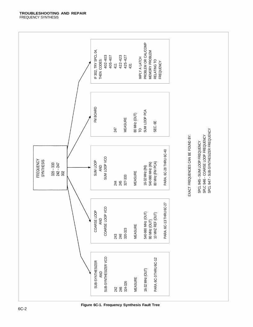
TROUBLESHOOTING AND REPAIRFREQUENCY SYNTHESIS
6C-2Figure 6C-1. Frequency Synthesis Fault Tree
IF 3
02, T
RY
SPC
L 04
,TH
EN C
OD
ES:
40
2-4
03
405-
407
411
422-
423
42
5-4
27
431
IMPL
Y A
LATC
HPR
OBL
EM O
R C
AL/C
OM
PM
EMO
RY
PRO
BLEM
REL
ATIN
G T
OFR
EQU
ENC
Y
FM B
OAR
D
247
MEA
SUR
E
80 M
Hz (O
UT)
TO SUM
LO
OP
PCA
SEC
. 6E
SUM
LO
OP
AND
SUM
LO
OP
VCO
244
245
327-
333
MEA
SUR
E
16-3
2 M
Hz (I
N)
540-
980
MH
z (IN
)80
MHz
(FM
PC
A)
PAR
A. 6
C-2
8 TH
RU
6C
-40
CO
ARSE
LO
OP
AND
CO
ARSE
LO
OP
VCO
243
246
320-
323
MEA
SUR
E
540-
980
MH
z (O
UT)
80 M
Hz (O
UT)
10 M
HZ R
EF (O
UT)
PAR
A. 6
C-1
3 TH
RU
6C
-27
SUB-
SYN
THES
IZER
AND
SUB-
SYN
THES
IZER
VC
O
242
246
324-
326
MEA
SUR
E
16-3
2 M
Hz (O
UT)
PAR
A. 6
C-3
TH
RU
6C
-12
EXAC
T FR
EQU
ENC
IES
CAN
BE
FOUN
D B
Y:
SPC
L 94
5 - S
UM
LO
OP
FREQ
UEN
CY
SPLC
946
- C
OAR
SE L
OO
P FR
EQU
ENC
YSP
CL
947
- SU
B-SY
NTH
ESIZ
ER F
REQ
UEN
CY
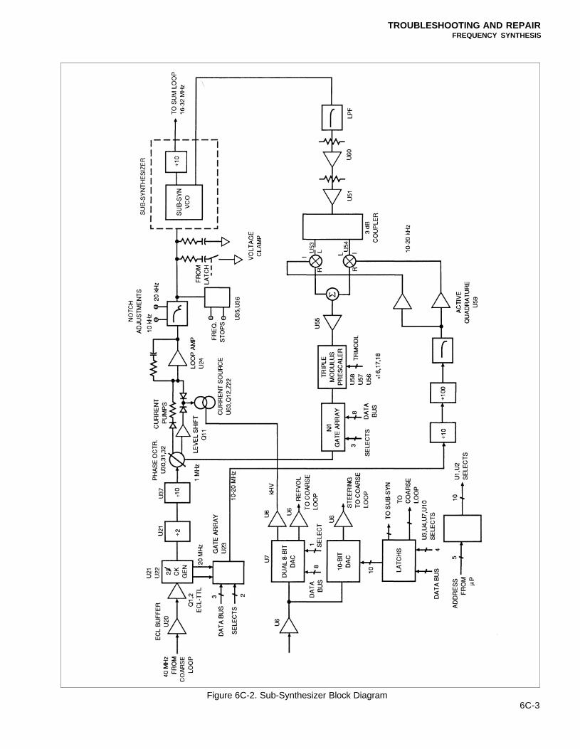
TROUBLESHOOTING AND REPAIRFREQUENCY SYNTHESIS
6C-3Figure 6C-2. Sub-Synthesizer Block Diagram
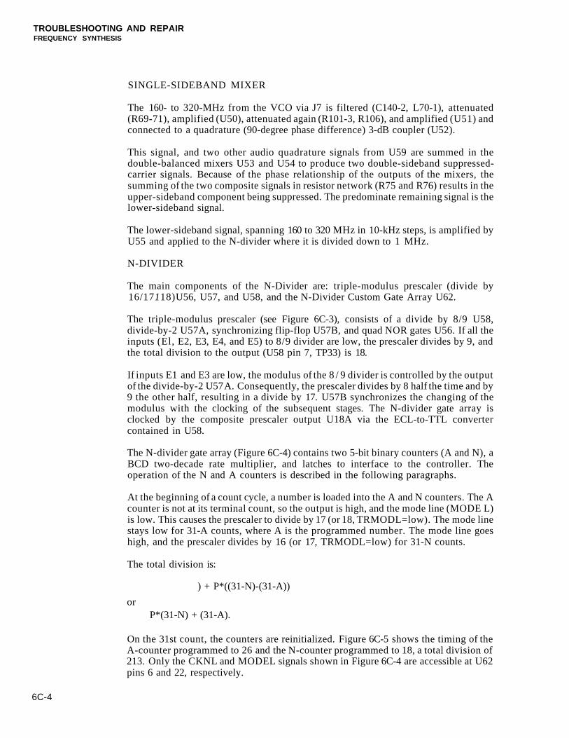
TROUBLESHOOTING AND REPAIRFREQUENCY SYNTHESIS
SINGLE-SIDEBAND MIXER
The 160- to 320-MHz from the VCO via J7 is filtered (C140-2, L70-1), attenuated(R69-71), amplified (U50), attenuated again (R101-3, R106), and amplified (U51) andconnected to a quadrature (90-degree phase difference) 3-dB coupler (U52).
This signal, and two other audio quadrature signals from U59 are summed in thedouble-balanced mixers U53 and U54 to produce two double-sideband suppressed-carrier signals. Because of the phase relationship of the outputs of the mixers, thesumming of the two composite signals in resistor network (R75 and R76) results in theupper-sideband component being suppressed. The predominate remaining signal is thelower-sideband signal.
The lower-sideband signal, spanning 160 to 320 MHz in 10-kHz steps, is amplified byU55 and applied to the N-divider where it is divided down to 1 MHz.
N-DIVIDER
The main components of the N-Divider are: triple-modulus prescaler (divide by16/17118) U56, U57, and U58, and the N-Divider Custom Gate Array U62.
The triple-modulus prescaler (see Figure 6C-3), consists of a divide by 8/9 U58,divide-by-2 U57A, synchronizing flip-flop U57B, and quad NOR gates U56. If all theinputs (El, E2, E3, E4, and E5) to 8/9 divider are low, the prescaler divides by 9, andthe total division to the output (U58 pin 7, TP33) is 18.
If inputs E1 and E3 are low, the modulus of the 8 / 9 divider is controlled by the outputof the divide-by-2 U57 A. Consequently, the prescaler divides by 8 half the time and by9 the other half, resulting in a divide by 17. U57B synchronizes the changing of themodulus with the clocking of the subsequent stages. The N-divider gate array isclocked by the composite prescaler output U18A via the ECL-to-TTL convertercontained in U58.
The N-divider gate array (Figure 6C-4) contains two 5-bit binary counters (A and N), aBCD two-decade rate multiplier, and latches to interface to the controller. Theoperation of the N and A counters is described in the following paragraphs.
At the beginning of a count cycle, a number is loaded into the A and N counters. The Acounter is not at its terminal count, so the output is high, and the mode line (MODE L)is low. This causes the prescaler to divide by 17 (or 18, TRMODL=low). The mode linestays low for 31-A counts, where A is the programmed number. The mode line goeshigh, and the prescaler divides by 16 (or 17, TRMODL=low) for 31-N counts.
The total division is:
) + P*((31-N)-(31-A))
orP*(31-N) + (31-A).
On the 31st count, the counters are reinitialized. Figure 6C-5 shows the timing of theA-counter programmed to 26 and the N-counter programmed to 18, a total division of213. Only the CKNL and MODEL signals shown in Figure 6C-4 are accessible at U62pins 6 and 22, respectively.
6C-4
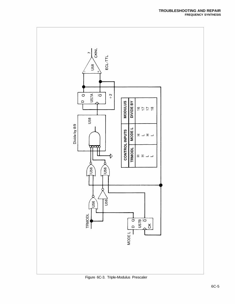
TROUBLESHOOTING AND REPAIRFREQUENCY SYNTHESIS
Figure 6C-3. Triple-Modulus Prescaler
6C-5
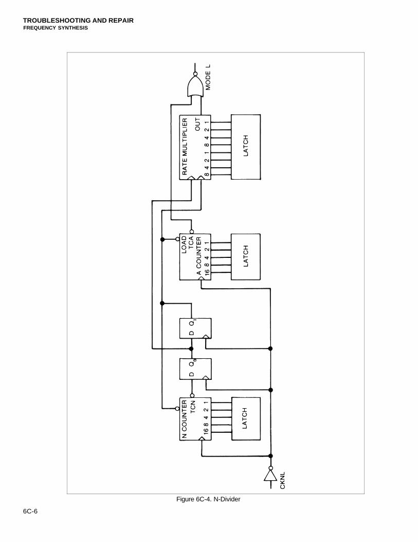
TROUBLESHOOTING AND REPAIRFREQUENCY SYNTHESIS
6C-6
Figure 6C-4. N-Divider
TROUBLESHOOTING AND REPAIRFREQUENCY SYNTHESIS
Figure 6C-5. N-Divider Timing Diagram
6C-7
CK
NL
A C
OU
NT
ER
TC
AL
N C
OU
NT
ER
TC
NL
Q0L
QIL
=L
OA
DL
RM
OU
TH
MO
DE
L
TROUBLESHOOTING AND REPAIRFREQUENCY SYNTHESIS
The N-divider gate array includes a two-decade rate multiplier that produces thefractional part of the division. The N-divider gate array rate multiplier produces apulse train with a programmed number of pulses for a 100-cycle frame of the 1-MHzN-divider output.
The programmed number ranges between zero and 99, corresponding to 10-kHz stepsat the VCO frequency. The flip-flops in the rate multiplier get set up on count 29, andon count 30 a pulse may or may not be present, depending on the programming of therate multiplier. This is the shaded pulse in the timing diagram (Figure 6C-5).
Irregularly spaced rate-multiplier pulses cause the mode line to go low, and theprescaler divides by P+l at a rate equal to the rate multiplier programming.
A 16/17 dual-modulus prescaler will not allow division from 160 to 320 without holes.For example, 170 is ten frames of 17. Consequently, there is no place to slip in therate-multiplier pulses. It is not possible to divide by 171.
By using a triple-modulus prescaler, these problems are solved. Continuing with theprevious example, 170 is 10 frames of 17 and 0 frames of 18. The deleter allows theprescaler to divide by 18 at a rate equal to the rate-multiplier frequency. Number 171 is9 frames of 17 and 1 frame of 18. A software algorithm determines whether to operatein the 16/17 mode (TRMODL=1) or 17/18 mode (TRMODL=0).
The frequency at the output of the N-divider gate array is (Fo - Fs - Fd)/N. Since thismust be equal to reference frequency, Fr, and Fr is 1 MHz, the VCO frequency is Fo =N + Fs + Fd, where Fs is the SSB audio frequency from the low order digit generator,and Fd is the fractional-division frequency.
PHASE DETECTOR
The 1-MHz reference signal from divide-by-10 U37, and the 1-MHz signal from theN-divider U62 are connected to a digital phase-frequency detector (U30, U31, U32). Ifthe N-divider output frequency is less than the reference frequency, TP25 is low, andthe voltage at the output of level shifter Q17 is below ground. This results in turning offCR18 and allowing current from U63 to flow through CR18 out of the integrator. Thisraises the voltage at the output of the integrator, which raises the VCO frequency.
Similarly, if the N-divider output frequency is above the reference, TP24 is highturning on CR16 and allowing current to flow through R97 into the integrator. Thislowers the voltage at the output of the integrator, which lowers the VCO frequency. Ifthe phase between the reference and N-divider output slips more than two cycles ineither direction, the corresponding phase-detector output is high or low. This providestwice the integrator current during acquisition as a conventional phase-frequencydetector.
R51 provides a small bias current to the integrator to bias the phase detector in thelinear region; consequently, the up-pump is always on.
During calibration of the VCO, the Kv, the VCO gain coefficient is measured at manyfrequencies across the band, and compensation data is stored in non-volatile memory.The instrument software uses this data along with N to control the PLL bandwidth.The PLL bandwidth is controlled by changing the current to the up-pump via KNDAC (U7A, U6A), and the voltage-to-current converter, U62 and Q12.
6C-8
TROUBLESHOOTING AND REPAIRFREQUENCY SYNTHESIS
LOOP AMPLIFIER
The loop amplifier-integrator consists of operational amplifier U34, C98, and R44.Capacitors C97 and C102 filter the 1-MHz reference. The output of the integrator isconnected to a multi-pole LC filter (R45, C104, C105, C106, C107, L56, L57, and R48)that attenuates the delete rate (10 and 20 kHz), and reference 1-MHz spurs.
Diodes CR12, CR13, CR14, CR15, CR22 and CR23 speedup the loop duringswitching. Additional lead/lag compensation is provided by C114, C115, R58, andR59. The second lead/lag network is switched by Q10 when the VCO frequency isabove 230 MHz. This is necessary to compensate for the wide Kv range of the VCO.
Amplifier U35 is a precision clamp to keep the VCO frequency within a specified range.The photoisolator U36 detects when the clamp is active, indicating an out-of-lockcondition. This signal is sent to the controller as the SUBUNLKL status.
LOW ORDER DIGITS GENERATOR
The low order digits generator consists of the clock generator (U21, U22, Q1, Q2), thegate array U23, the divide-by-1000 (U60, U61), the low-pass filter (L75, L76), and theactive quadrature generator, U59. Internal to the gate-array U23 is a 3 ½ decade-ratemultiplier, associated latches, and a divide-by-2.
The 40-MHz reference from the Coarse Loop is converted to ECL in U20 and thenconverted to TTL in Ql and Q2. This is followed by a 20-MHz two-phase clockgenerator U21, U22.
The input frequency to the rate multiplier is 20 MHz. The output frequency can beprogrammed from zero to 19.995 MHz in 5-kHz steps. This signal is ORd with theother phase of the 20-MHz clock to produce 20 to 39.995 MHz at U23 pin 1. The signalis also divided by 2 in U23, by 10 in U60, and again by 100 in U61 to produce 10 to19.99975 kHz in 2.5-Hz steps. Not all of this resolution is utilized. This TTL signal atTP30 is filtered by L75, L76, C156, C157, C158, C159, and C160. Op-amp U59 formsan active quadrature generator such that the signal at output pins 7 and 14 are offset by90 degrees. These two signals are the 10- to 20-kHz inputs for the PLL single-sidebandmixer.
DACS AND LATCHES
The control bits for the Coarse Loop PCA are latched by U3, part of U9 and U10.DAC U5 with op-amp U6D provides the steering voltage for the Coarse Loop VCOand DAC U7B with op-amp U6B provides the voltage to tune the reference TXCO.
SUB-SYNTHESIZER TROUBLESHOOTING 6C-4.
NOTE
AII frequencies mentioned are synthesized; hence they are exact (coherentwith the 10-MHz reference), unless noted as approximate.
Status code 242 indicates that the Sub-Synthesizer and/or Sub-Synthesizer VCO isnot functioning properly. This status code is triggered when the Sub-Synthesizer VCOcontrol voltage is out of the normal operating range. A status code 244, which indicatesthat the Sum Loop is out of lock, might also indicate a problem with theSub-Synthesizer and/or Sub-Synthesizer VCO.
6C-9
TROUBLESHOOTING AND REPAIRFREQUENCY SYNTHESIS
Status code 244, appearing without status code 242, might indicate a marginalbreak-up condition. To check the Sub-Synthesizer across the band, move the jumperon the Sub-Synthesizer VCO (A3) from TP1-TP2 to TP1-TP3. This allows theSub-Synthesizer VCO frequency, not divided, to appear at A3-J2. Connect this outputto a spectrum analyzer. Program the signal generator to 800 MHz. There should be astable signal at 160 MHz displayed on the spectrum analyzer. Step the signal generatorin 200-kHz steps, while stepping the spectrum analyzer in 4-MHz steps. At each point,a stable signal should be displayed on the spectrum analyzer. If the signal showsevidence of breaking up, there is a problem with the Sub-Synthesizer and/orSub-Synthesizer VCO.
If there is a status code 242, check to see if the VCO control voltage is stuck high or low.A good way to do this is to measure the DC voltage at TP27. This test point can beaccessed without removing the module cover. If the DC voltage is around 1.5V, theproblem is in the circuitry that supplies the 1-MHz reference or in the phase detectorcircuit; if it is around 23V, the problem is associated with the whole phase lock loop(VCO, SSB mixer, divider).
Table 6C-1 shows the characteristics of the signals at the various test points on theSub-Synthesizer PCA. The table gives the range of the signal and the expected valuefor a typical instrument state. The values in the typical apply when the signal generatoris programmed to 804.001499 MHz. In this troubleshooting procedure it is useful tohave the undivided Sub-Synthesizer VCO signal available. On the Sub-SynthesizerVCO (A3), move the jumper from TP1-TP2 to TP1-TP3.
If the voltage at TP27 is approximately 1.5 volts, check TP22. There should be a1-MHz TTL square wave. If the signal is missing or the frequency is incorrect, workbackwards from this point. If this frequency is correct, the problem is probably in thephase detector (U30-32) or loop amplifier (U34, etc.). At U21-9 there should be a10-MHz TTL square wave. The input, U21-11, should be a 20-MHz TTL square wave.At U21-3 there should be a 40-MHz TTL signal. There should be a 40-MHz ECL signalat both U20-2 and U20-14. The frequency input, J6, from the Coarse Loop (A2),should be approximately a 600-mV, p-p 40-MHz signal.
If the voltage at TP27 is around 23V, remove the shorting jumper connectingTP40-TP41 and connect a variable power supply to TP41, being careful not the shortto TP40 which could destroy U34. This opens the loop and allows the frequency of theSub-Synthesizer VCO to be controlled directly. Use a spectrum analyzer or counterconnected to the undivided Sub-Synthesizer VCO output (A3-J3) to monitor thefrequency. Adjust the power supply so that the frequency tunes from approximately160 to 320 MHz. If the frequency cannot be adjusted, the problem is probably in theSub-Synthesizer VCO (A3). Set the frequency to approximately 240 MHz with thevariable power supply.
Using a spectrum analyzer and the low impedance probe, with the 10X attenuator,measure the level at the output of U51. A good place to measure this is at the input tothe coupler, U52. Note that the low impedance probe should be grounded as closely aspossible. PCA hold-down screws and the walls of the plate provide good grounds. Thelevel at this point should be approximately -10 dBm as measured on the spectrumanalyzer. Troubleshoot the RF section (U50, U51, etc.) if this level is not correct.
6C-10
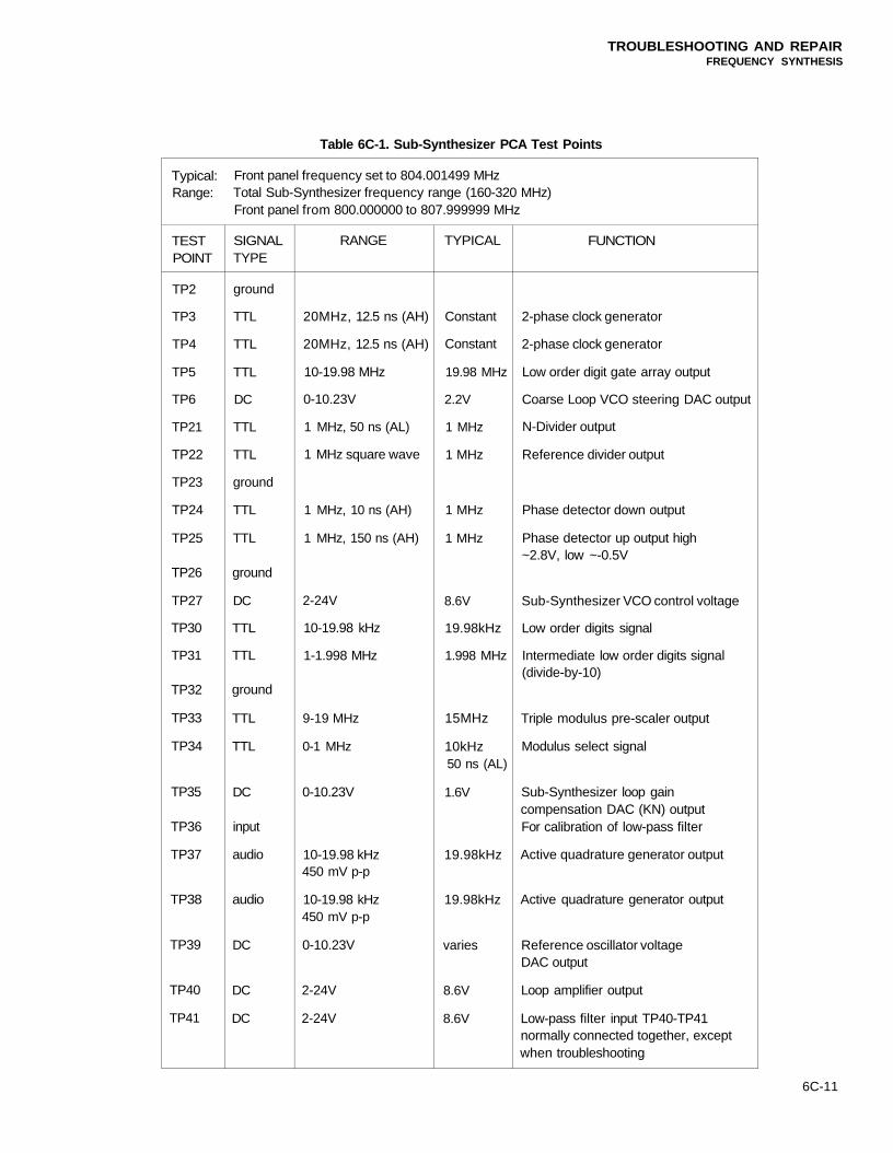
TROUBLESHOOTING AND REPAIRFREQUENCY SYNTHESIS
Table 6C-1. Sub-Synthesizer PCA Test Points
6C-11
Typical:Range:
TESTPOINT
TP2
TP3
TP4
TP5
TP6
TP21
TP22
TP23
TP24
TP25
TP26
TP27
TP30
TP31
TP32
TP33
TP34
TP35
TP36
TP37
TP38
TP39
TP40
TP41
Front panel frequency set to 804.001499 MHzTotal Sub-Synthesizer frequency range (160-320 MHz)Front panel from 800.000000 to 807.999999 MHz
SIGNALTYPE
ground
TTL
TTL
TTL
DC
TTL
TTL
ground
TTL
TTL
ground
DC
TTL
TTL
ground
TTL
TTL
DC
input
audio
audio
DC
DC
DC
RANGE
20MHz, 12.5 ns (AH)
20MHz, 12.5 ns (AH)
10-19.98 MHz
0-10.23V
1 MHz, 50 ns (AL)
1 MHz square wave
1 MHz, 10 ns (AH)
1 MHz, 150 ns (AH)
2-24V
10-19.98 kHz
1-1.998 MHz
9-19 MHz
0-1 MHz
0-10.23V
10-19.98 kHz450 mV p-p
10-19.98 kHz450 mV p-p
0-10.23V
2-24V
2-24V
TYPICAL
Constant
Constant
19.98 MHz
2.2V
1 MHz
1 MHz
1 MHz
1 MHz
8.6V
19.98kHz
1.998 MHz
15MHz
10kHz50 ns (AL)
1.6V
19.98kHz
19.98kHz
varies
8.6V
8.6V
FUNCTION
2-phase clock generator
2-phase clock generator
Low order digit gate array output
Coarse Loop VCO steering DAC output
N-Divider output
Reference divider output
Phase detector down output
Phase detector up output high~2.8V, low ~-0.5V
Sub-Synthesizer VCO control voltage
Low order digits signal
Intermediate low order digits signal(divide-by-10)
Triple modulus pre-scaler output
Modulus select signal
Sub-Synthesizer loop gaincompensation DAC (KN) outputFor calibration of low-pass filter
Active quadrature generator output
Active quadrature generator output
Reference oscillator voltageDAC output
Loop amplifier output
Low-pass filter input TP40-TP41normally connected together, exceptwhen troubleshooting
TROUBLESHOOTING AND REPAIRFREQUENCY SYNTHESIS
Next, use the low impedance probe to check the signal at the input to the divider (U58)at pin 15. There should be a -15 dBm lower sideband signal as measured on thespectrum analyzer. A problem at this point indicates a problem in the low order digitsgenerator (U21, U22, U23, U60, U61), active quadrature generator (U59), the SSBmixer (U53, U54), or the divider input amplifier (U55).
Program the signal generator to 804.000500 MHz. The signal at the output of the triplemodulus prescaler, TP33, should be an approximately 15-MHz TTL signal. The signalat the output of the N-divider gate array, TP34, should be approximately 1 MHz. Asthe 1-MHz digit is programmed, this frequency should change, since the divide ratio ischanging.
To troubleshoot the low order digit generator, check the signal at TP3 and TP4. Thereshould be a 25% duty cycle, active high 20-MHz TTL signal. Program the signalgenerator to 800.000000 MHz. The signal at TP5 should be 10 MHz TTL. As youprogram the UUT to 1 Hz, 10 Hz, and 100 Hz digits, the frequency at TP5 shouldchange by 20 kHz, 200 kHz, and 2 MHz, respectively. When the UUT is programmedto 800.000499 MHz, the frequency at TP5 should be 19.98 MHz. The outputs of thetwo divide-by-10, U60, U61 should be 1.998 MHz and 19.98 kHz, respectively. Theoutput of the active quadrature generator, U59, at TP37 and TP38 should beapproximately 450-mV p-p 19.98-kHz sine waves.
Monitor the frequency at TP21 as you tune the power supply. If the frequency is below240 MHz, the frequency at TP21 should be below 1 MHz. There should be a TTLsignal at TP24 that is predominantly low with very thin pulses going high. Thereshould be a similar signal at TP25, except the "low" voltage is approximately -0.5V andthe "high" voltage is +2.8 V. The voltage at TP40 should be about 28V. If the frequencyis above 240 MHz, the frequency at TP21 should be above 1 MHz. The signal levels atTP24 and TP25 should be predominantly high. The voltage at TP40 should be about-2V. If the signals at TP24 and TP25 are correct, but the voltage at TP40 does notchange from approximately -2V to +28V as the frequency at TP21 is adjusted aboveand below 1 MHz, the problem is probably in the loop amplifier (U34, etc.), the currentsource (U63, etc.), the switching diodes (CR18, CR19), or the KN DAC (U6, U7, etc.).The loop should lock when you reconnect the shorting jumper between TP40 andTP41. If the loop doesn't lock, the final circuitry to check is the low-pass filter (L56,L57, etc.), the clamp circuit (U35, U36, etc.), and the lead-lag network. FET Q10should be on (~+5 V on the gate) below a undivided Sub-Synthesizer frequency of 230MHz and off (~0V on the gate) above 230 MHz. You can disable the clamp circuit bydisconnecting CR20 and CR21.
To check the various DACs, program the UUT to SPCL 943. This sets all the DACs atfull scale. The voltage at the output of the KN DAC (TP35), REFVOL DAC (TP39)and STEERING DAC (TP6) should be approximately 10.23V. With the UUTprogrammed to SPCL 942, which sets the DACs to half scale, the voltages should beabout 5.12V.
6C-12
TROUBLESHOOTING AND REPAIRFREQUENCY SYNTHESIS
SUB-SYNTHESIZER ADJUSTMENTS 6C-5.
The following procedures cover the five adjustments on the A4 Sub-Synthesizer PCAlisted below:
R5, DAC Full Scale AdjustmentR99, Clamp AdjustmentR98, Clamp AdjustmentR106, Mixer LO Drive AdjustmentL56, 10 kHz Notch Adjustment
Note that these adjustments are not routine and are required only when associatedcomponents have been replaced, or when the adjustment has been changed or hasshifted.
Steering DAC Full Scale Adjustment 6C-6.
TEST EQUIPMENT:
• DVM
REMARKS:
Steering DAC Full Scale adjustment is normally required only when U5, U6, orassociated components have been replaced, or when the adjustment has shifted.
PROCEDURE:
The Steering DAC voltage is adjusted to 10.23V with the Coarse Loop Steering DACset to full scale.
1. Program the UUT to SPCL 909.
2. Program the UUT to SPCL 943. This Special Function programs all DACs to fullscale.
3. Connect the DVM to measure voltage between TP6 and ground.
4. Adjust R5 for 10.23V ± 0.01V.
5. Program the UUT to SPCL 00. This clears all Special Functions.
Lower Clamp Adjustment, R99 6C-7.
TEST EQUIPMENT:
• Frequency counter
REMARKS:
The Lower Clamp Adjustment (R99) is normally required only when U35, U36 orassociated components have been replaced, when the Sub-Synthesizer VCO (A3) hasbeen repaired or replaced, or when the adjustment has shifted.
6C-13
TROUBLESHOOTING AND REPAIRFREQUENCY SYNTHESIS
PROCEDURE:
The Lower Clamp frequency is adjusted to 15 MHz with the reference to the phasedetector disabled.
1. Connect output (J4) of the Sub-Synthesizer VCO (A3) to the frequency counter.Set the frequency counter to measure with 1-kHz resolution.
2. Program the UUT to SPCL 909.
3. Program the UUT to 800 MHz. Frequency counter should read 16.000 MHz.
4. Short TP22 to ground.
5. Adjust R99 so that the frequency counter reads 15.000 MHz ± 10 kHz.
Upper Clamp Adjustment, R98 6C-8.
TEST EQUIPMENT:
• Frequency counter
REMARKS:
The Upper Clamp Adjustment, R98 is normally required only when U35, U36 orassociated components have been replaced, when the Sub-Synthesizer VCO (A3) hasbeen repaired or replaced, or when the adjustment has shifted.
PROCEDURE:
The Upper Clamp frequency is adjusted to 32.5 MHz with the N-divider signal to thephase detector disabled.
1. Connect output (J4) of the Sub-Synthesizer VCO (A3) to the frequency counter.Set the frequency counter to measure with 1-kHz resolution.
2. Program the UUT to SPCL 909.
3. Program the UUT to 640 MHz. Frequency counter should read 32.000 MHz.
4. Short TP21 to ground.
5. Adjust R98 so that the frequency counter reads 32.500 MHz ± 10 kHz.
SSB Mixer LO Drive Adjustment, R106 6C-9.
TEST EQUIPMENT:
• RF Probe (10X)• Spectrum analyzer
REMARKS:
The SSB Mixer LO Drive Adjustment (R106) is normally required only when U50,U51 or associated components have been replaced, when the Sub-Synthesizer VCO(A3) has been repaired or replaced, or when the adjustment has shifted.
6C-14
TROUBLESHOOTING AND REPAIRFREQUENCY SYNTHESIS
PROCEDURE:
The SSB Mixer LO Power, as measured with a 10X RF probe using a spectrumanalyzer, is adjusted to -10 dBm as displayed on the spectrum analyzer. Thiscorresponds to +10 dBm at the input to the coupler.
1. Program the UUT to SPCL 909.
2. Program the UUT to 800 MHz.
3. Connect the 10X RF probe to the input of the spectrum analyzer. Set the spectrumanalyzer to -5 dBm reference level, 160 MHz, 1-MHz span, and 1 dB/div.
4. Touch the probe tip to input of the coupler, U52, that connects to C147. This is bestdone on the top of the coupler with the ground connection on the coupler groundplane.
5. Adjust R106 for -10 dBm as displayed on the spectrum analyzer.
10-kHz Notch Adjustment, L56 6C-10.
TEST EQUIPMENT:
• Spectrum analyzer
REMARKS:
The 10-kHz Notch Adjustment is normally required only when L56, L57 andassociated components have been replaced or the adjustment has shifted.
PROCEDURE:
A signal from the internal modulation oscillator is injected into the Sub-Synthesizerphase detector to produce a 10-kHz spur. L56 is adjusted to minimize this spur.
1. Program UUT to SPCL 909.
2. On Sub-Synthesizer VCO (A3), move jumper (near J2) from TP1-TP2 toTP1-TP3. Replace the cover on this side of the module.
3. Program the UUT to 800 MHz, Modulation Frequency 10 kHz, Modulation Levelto 100 mV. Connect the front panel mod out to TP36 on Sub-Synthesizer PCA.
4. Set spectrum analyzer to center 160 MHz, reference level 5 dBm, frequency span100 kHz. The signal should be visible in the center of the screen with 10-kHzsidebands.
5. Adjust L56 to minimize these 10-kHz sidebands.
6. On the Sub-Synthesizer VCO (A3), move jumper (near J2) back to TP1-TP2.
6C-15
TROUBLESHOOTING AND REPAIRFREQUENCY SYNTHESIS
SUB-SYNTHESIZER VCO (A3) CIRCUIT DESCRIPTION 6C-11.
The A3 Sub-Synthesizer VCO PCA is controlled by the A4 Sub-Synthesizer PCA andproduces a signal that is further processed in the A12 Sum Loop PCA. This assemblyincludes a varactor tuned oscillator that generates frequencies from 160 to 320 MHz,along with low-pass filters and an ECL divide-by-ten circuit.
Ql is configured as an oscillator, with a tunable resonant circuit connected betweenbase and collector that provides positive feedback. This circuit includes printedtransmission lines, varactor diodes CR1-CR4, and inductor L1. The frequency tuningvoltage at J1-4 is applied to the varactor diodes through RF choke L2, and tunes theoscillator over the range of 160-320 MHz with voltages from about 2V to 22V.
The oscillator transistor output signal at Q1 emitter is next applied to Q2, configuredas a common-base stage that provides isolation. The 0 dBm output of Q2 is applied tomonolithic amplifier U1, which boosts the signal level to +13 dBm at its output.
Two switched low-pass filters, including PIN diodes CR5-CR8 and capacitorsC13-C22, follow U1 and provide harmonic suppression. Comparator U4 senses thetuning voltage, VT, and enables the low band filter between CR5 and CR6 for VT lessthan 7.5V, and enables the high band filter between CR7 and CR8 for VT greater than7.5V. The switching voltage, 7.5V, corresponds to about 230 MHz.
The filtered signal is next applied to resistive splitter R13-R17. One output drivesmonolithic amplifier U2, which provides isolation and boosts the signal to about +7dBm. This signal connects to the A4 Sub-Synthesizer PCA by a through-the-platecoaxial connector at P1. The other splitter output drives ECL frequency divider U3,which is configured to divide by ten. The divided output signal from U3 is filtered by afive-element low-pass filter (L5, L6, C27-C29), and connects to the A12 Sum LoopPCA at J2 by a coaxial cable. This signal ranges in frequency from 16 to 32 MHz.
SUB-SYNTHESIZER VCO TROUBLESHOOTING 6C-12.
A problem in the Sub-Synthesizer VCO can cause uncal status response 242(Sub-Synthesizer unlock) and can also cause self-test failure 324. To test the VCOindependent of the Sub-Synthesizer PCA, a voltage source, such as a lab power supply,can be connected to the phase lock port at J1 pin 4. This will override the voltagesupplied by the Sub-Synthesizer PCA and won't cause damage. Vary the phase lockvoltage from 2 to 23V, and observe the signal at connector J2 on a spectrum analyzer.The frequency should vary from about 16 to 32 MHz, and the level should be about +2dBm. If the signal is not as described, the VCO is likely faulty. As a first step introubleshooting, remove the plug-on jumper that connects TP1 and TP2, and install itto connect TP1 to TP3. This bypasses divider U3, and connects the fundamentaloscillator signal to J2. This signal should vary from about 160 to 320 MHz at about +3dBm over the tuning range. If this signal is faulty, the circuit prior to U3 is faulty.Remember to replace the plug-on jumper in its original position after troubleshooting.DC voltages can be readily measured at various nodes in the circuit, and may help toisolate the faulty circuit. Table 6C-2 lists expected approximate DC voltages at variouscircuit nodes, as an aid to troubleshooting.
6C-16
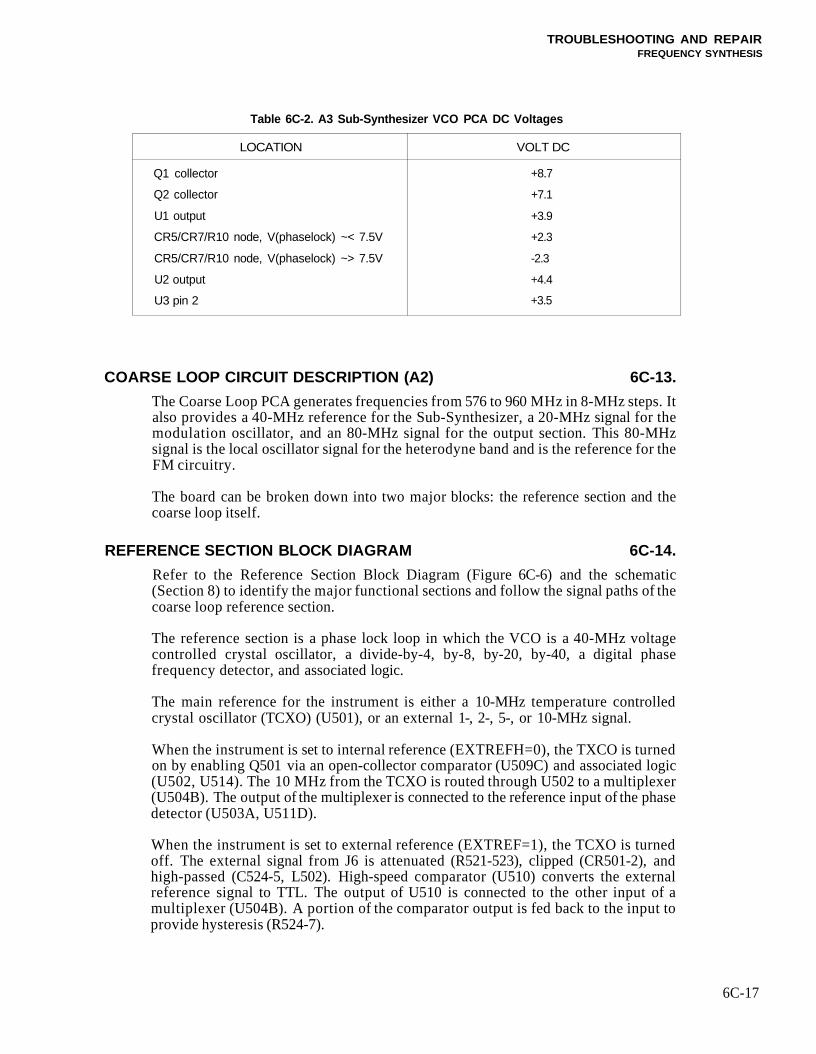
TROUBLESHOOTING AND REPAIRFREQUENCY SYNTHESIS
Table 6C-2. A3 Sub-Synthesizer VCO PCA DC Voltages
COARSE LOOP CIRCUIT DESCRIPTION (A2) 6C-13.
The Coarse Loop PCA generates frequencies from 576 to 960 MHz in 8-MHz steps. Italso provides a 40-MHz reference for the Sub-Synthesizer, a 20-MHz signal for themodulation oscillator, and an 80-MHz signal for the output section. This 80-MHzsignal is the local oscillator signal for the heterodyne band and is the reference for theFM circuitry.
The board can be broken down into two major blocks: the reference section and thecoarse loop itself.
REFERENCE SECTION BLOCK DIAGRAM 6C-14.
Refer to the Reference Section Block Diagram (Figure 6C-6) and the schematic(Section 8) to identify the major functional sections and follow the signal paths of thecoarse loop reference section.
The reference section is a phase lock loop in which the VCO is a 40-MHz voltagecontrolled crystal oscillator, a divide-by-4, by-8, by-20, by-40, a digital phasefrequency detector, and associated logic.
The main reference for the instrument is either a 10-MHz temperature controlledcrystal oscillator (TCXO) (U501), or an external 1-, 2-, 5-, or 10-MHz signal.
When the instrument is set to internal reference (EXTREFH=0), the TXCO is turnedon by enabling Q501 via an open-collector comparator (U509C) and associated logic(U502, U514). The 10 MHz from the TCXO is routed through U502 to a multiplexer(U504B). The output of the multiplexer is connected to the reference input of the phasedetector (U503A, U511D).
When the instrument is set to external reference (EXTREF=1), the TCXO is turnedoff. The external signal from J6 is attenuated (R521-523), clipped (CR501-2), andhigh-passed (C524-5, L502). High-speed comparator (U510) converts the externalreference signal to TTL. The output of U510 is connected to the other input of amultiplexer (U504B). A portion of the comparator output is fed back to the input toprovide hysteresis (R524-7).
6C-17
LOCATION
Q1 collector
Q2 collector
U1 output
CR5/CR7/R10 node, V(phaselock) ~< 7.5V
CR5/CR7/R10 node, V(phaselock) ~> 7.5V
U2 output
U3 pin 2
VOLT DC
+8.7
+7.1
+3.9
+2.3
-2.3
+4.4
+3.5
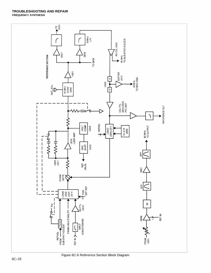
TROUBLESHOOTING AND REPAIRFREQUENCY SYNTHESIS
6C-18Figure 6C-6 Reference Section Block Diagram
TROUBLESHOOTING AND REPAIRFREQUENCY SYNTHESIS
The 40-MHz voltage-controlled crystal oscillator (VCXO) consists of the 40-MHzthird overtone crystal (Y601), a grounded base stage (Q606 and associated com-ponents), a low Q tuned circuit to ensure the crystal operates at the third overtone(L601, C604-5, R602), and varactors (CR603-5). This oscillator can be tunedapproximately ± 1 kHz. The feedback is from the collector to the emitter. The output,from the collector tuned circuit is lightly coupled (C607) to a buffer amplifier (U601).The output of the buffer is connected to the 80-MHz section (R606, R617, C610) andanother pair of grounded base stages (Q607-8). The outputs of these buffers arelow-pass filtered (C616-17, L604 and C622-23, L605). One output is converted to ECL(U602), and the other output drives the main loop phase detector buffer amplifier(Q205).
One output of U602 provides the 40-MHz reference for the Sub-Synthesizer via J16.The other output is divided by 2 (U506A) and buffered by U513. The 20-MHz squarewave output is band-pass filtered (R36, L510, C545) before being sent to themodulation oscillator (J8). A second divide-by-2 (U506B) divides the 20 MHz to 10MHz. This ECL signal is converted to TTL (Q504-05) and buffered (U507C). Twoinverters in parallel (U507A,B) drive a low pass-filter (C518-19, C550, L501) whoseoutput is a 10-MHz sine wave. This is the reference out for the instrument (J7).
When in internal reference, the 10-MHz signal from U507C is routed through amultiplexer (U504A) to the R input of the phase frequency detector (U503B, U511D).When in external reference (10 MHz), divider U505 is disabled and the signal fromU507C is routed through a multiplexer (U504C), logic (U511 A,B) to the R input of thephase frequency detector. When Special Function 761 is enabled, the 10-MHz signal isdivided down to either 1, 2, or 5 MHz (U505), depending on how the switches are set(S502). The output of the divider is also routed to the phase frequency detector.
The phase frequency detector (U503, U511D) compares the phase/frequency of thedivided down 40-MHz VCXO (V input) with either the 10-MHz TCXO or an externalreference. The phase detector normally operates at 10 MHz except when an externalreference of 1 ,2, or 5 MHz is used. In these cases, it operates at the reference frequency.The output of this phase detector operates in the differential voltage mode. If thefrequency/phase of the V input (U503B-11) is greater than the R input (U503A-3),there will be a net positive voltage from U503A-6 to U503B-8. The loop amplifier/integrator (U508 and associated components), which drives a lead-lag network (R532,R530, C546, Q502), integrates the phase detector voltage and causes the voltage on thecontrol line to the varactors (CR603-5) to drop until the two frequencies match and theloop is locked. Consequently, if the frequency/phase of the R input is greater than theV input, there will be a net negative voltage, and the control voltage will rise until theloop is locked. A small phase offset is set (R512) to keep the phase detector in its linearregion. The bandwidth of this reference loop is changed by switching in variouslead-lag networks (R505, R510, R530, R532, C530, C547, C549, C546). When ininternal TCXO or external 10 or 5 MHz, Q506 and Q502 are on and the loopbandwidth is approximately 30 Hz. When the external reference is 1 or 2 MHz, Q506 ison and Q502 is off. By turning Q502 off, the gain is increased 5 times, but since thedivision factor is 5 times greater, the overall loop gain remains approximatelyconstant. The loop control voltage (U508-6) is sensed by two comparators (U509A,B).If the voltage is below approximately 1.2V and above approximately 11V or there arepulses, this indicates the loop is unlocked. A one-shot (U512) converts these pulses intoa logic signal. This is combined with the low and high voltage detector to produceREFUNLKL, which is sent to the controller.
The 40 MHz from the buffer (U601) is amplified (Q609) and doubled to 80 MHz in afull wave rectifier (CR601, CR602, T601). The 80 MHz is filtered (L611, L612, C643,
6C-19
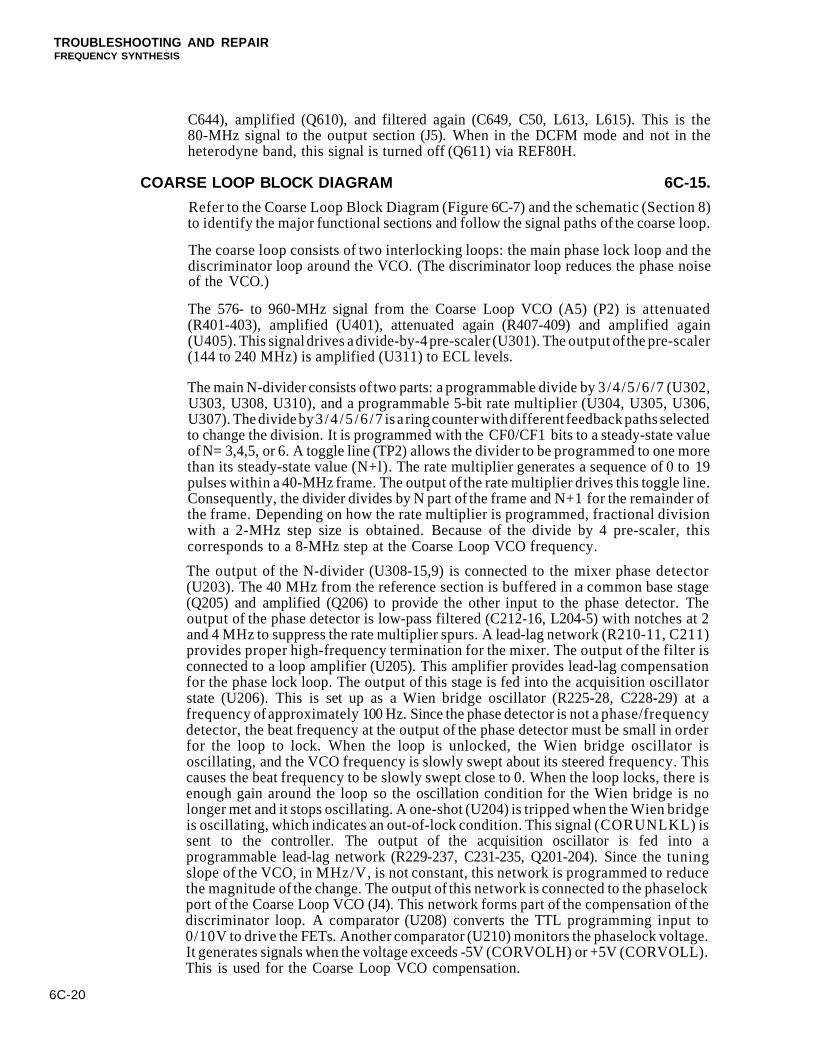
TROUBLESHOOTING AND REPAIRFREQUENCY SYNTHESIS
C644), amplified (Q610), and filtered again (C649, C50, L613, L615). This is the80-MHz signal to the output section (J5). When in the DCFM mode and not in theheterodyne band, this signal is turned off (Q611) via REF80H.
COARSE LOOP BLOCK DIAGRAM 6C-15.
Refer to the Coarse Loop Block Diagram (Figure 6C-7) and the schematic (Section 8)to identify the major functional sections and follow the signal paths of the coarse loop.
The coarse loop consists of two interlocking loops: the main phase lock loop and thediscriminator loop around the VCO. (The discriminator loop reduces the phase noiseof the VCO.)
The 576- to 960-MHz signal from the Coarse Loop VCO (A5) (P2) is attenuated(R401-403), amplified (U401), attenuated again (R407-409) and amplified again(U405). This signal drives a divide-by-4 pre-scaler (U301). The output of the pre-scaler(144 to 240 MHz) is amplified (U311) to ECL levels.
The main N-divider consists of two parts: a programmable divide by 3 /4 /5 /6 /7 (U302,U303, U308, U310), and a programmable 5-bit rate multiplier (U304, U305, U306,U307). The divide by 3 /4 /5 /6 /7 is a ring counter with different feedback paths selectedto change the division. It is programmed with the CF0/CF1 bits to a steady-state valueof N= 3,4,5, or 6. A toggle line (TP2) allows the divider to be programmed to one morethan its steady-state value (N+l). The rate multiplier generates a sequence of 0 to 19pulses within a 40-MHz frame. The output of the rate multiplier drives this toggle line.Consequently, the divider divides by N part of the frame and N+1 for the remainder ofthe frame. Depending on how the rate multiplier is programmed, fractional divisionwith a 2-MHz step size is obtained. Because of the divide by 4 pre-scaler, thiscorresponds to a 8-MHz step at the Coarse Loop VCO frequency.
The output of the N-divider (U308-15,9) is connected to the mixer phase detector(U203). The 40 MHz from the reference section is buffered in a common base stage(Q205) and amplified (Q206) to provide the other input to the phase detector. Theoutput of the phase detector is low-pass filtered (C212-16, L204-5) with notches at 2and 4 MHz to suppress the rate multiplier spurs. A lead-lag network (R210-11, C211)provides proper high-frequency termination for the mixer. The output of the filter isconnected to a loop amplifier (U205). This amplifier provides lead-lag compensationfor the phase lock loop. The output of this stage is fed into the acquisition oscillatorstate (U206). This is set up as a Wien bridge oscillator (R225-28, C228-29) at afrequency of approximately 100 Hz. Since the phase detector is not a phase/frequencydetector, the beat frequency at the output of the phase detector must be small in orderfor the loop to lock. When the loop is unlocked, the Wien bridge oscillator isoscillating, and the VCO frequency is slowly swept about its steered frequency. Thiscauses the beat frequency to be slowly swept close to 0. When the loop locks, there isenough gain around the loop so the oscillation condition for the Wien bridge is nolonger met and it stops oscillating. A one-shot (U204) is tripped when the Wien bridgeis oscillating, which indicates an out-of-lock condition. This signal (CORUNLKL) issent to the controller. The output of the acquisition oscillator is fed into aprogrammable lead-lag network (R229-237, C231-235, Q201-204). Since the tuningslope of the VCO, in MHz/V, is not constant, this network is programmed to reducethe magnitude of the change. The output of this network is connected to the phaselockport of the Coarse Loop VCO (J4). This network forms part of the compensation of thediscriminator loop. A comparator (U208) converts the TTL programming input to0/10V to drive the FETs. Another comparator (U210) monitors the phaselock voltage.It generates signals when the voltage exceeds -5V (CORVOLH) or +5V (CORVOLL).This is used for the Coarse Loop VCO compensation.
6C-20
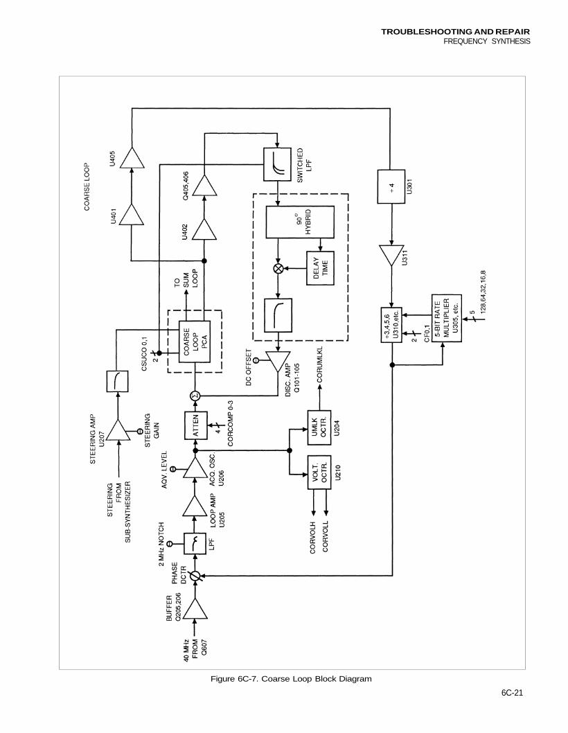
TROUBLESHOOTING AND REPAIRFREQUENCY SYNTHESIS
Figure 6C-7. Coarse Loop Block Diagram
6C-21
TROUBLESHOOTING AND REPAIRFREQUENCY SYNTHESIS
The steering voltage from the DAC on the Sub-Synthesizer PCA (J1-16), is amplifiedand filtered (U207) before it is sent to the Coarse Loop VCO (J15). This stage is a500-Hz active Bessel filter.
The discriminator "measures" the frequency noise of the VCO and generates acorrection signal to reduce the noise. A portion of the RF output from the CoarseLoop VCO (P2) is amplified (U402) and fed into a two stage limiting power amplifier(Q405-6). The output of the amplifier is filtered (C422-6, CR402-3). This filter isswitched at 712 MHz, the same point as a VCO band change. An op-amp (U209) drivesthe pin diode switches (CR402-3). The output power from the filter is approximately+20 dBm to the 90-degree power splitter on the Discriminator Board (A25). Theoutputs of the power splitter are connected to the LO input of the mixer (U404) and tothe delay cable. The other end of the delay cable is connected to the RF input of themixer. The delay cable is trimmed so that when the coarse loop steps in 8-MHzincrements, the phase is such that the IF output is approximately at 0V DC. A filter(C418-421, L403-4, R419-420) is connected to the IF port. This filter provides bothUHF and HF terminations for the mixer. The output of the filter is AC-coupled (C101,R106) to a low noise amplifier (Q101-106). The output of this amplifier is resistivelysummed (R123, R125) with the phaselock voltage from U206. Diodes (CR101-2) limitthe output of the discriminator amplifier while in the acquisition mode. To ensurestability, the gain of the low noise amplifier is rolled off (C104, R119).
COARSE LOOP TROUBLESHOOTING 6C-16.
The Coarse Loop (A2) can be broken up into two sections: the reference section andthe main coarse loop. These sections can be treated independently.
REFERENCE SECTION
A status code 246 indicates a problem in the reference section. If the unit is in externalreference and there is no reference supplied, or if the reference is the wrong frequencyor is outside of the lock range specification, a status code 246 will be displayed. If theunit is in internal reference and the high or medium stability option is installed, checkto see that the 10-MHz output from the option is correct.
Measure the voltage at TP19. If this voltage is approximately -13V, this indicates aproblem with the internal TCXO, the internal/external reference circuitry, or thephase detector/loop amplifier. If the voltage is approximately 13V, this indicates aproblem in the 40-MHz oscillator, buffers, dividers, or phase detector/loop amplifier.
If the voltage at TP19 is approximately 13V, first check the 40-MHz oscillator. Whenmeasuring signals with an oscilloscope all voltages are approximate. Use a 10-Meg, 8pfprobe. Make a ground connection at the probe tip with less than 1 inch of lead. Thereshould be a 40-MHz signal, 1.4V p-p at TP4. All frequencies are not exact because thereference loop is not locked and will typically be slightly higher than indicated. Afterthe buffers at the L605, C624, C625 and L605, C617, C625 junctions, this signal shouldbe 630 mV p-p. After the ECL buffer, at U602 pin 2, there should be a 40-MHz ECLsignal. At TP17, which connects to the Sub-Synthesizer (A4), there should be a 700 mVp-p signal. The output of the first divide-by-2, U506 pin 15, should be a 20-MHz ECLsquare wave. Following the buffer, U513, that supplies the modulation oscillator (A6),there should be a 20-MHz, 1.2V p-p signal at TP17. There should be a 10-MHz ECLsquare wave at U506 pins 2 and 3. At the collector of Q505, there should be a 10-MHzTTL signal. At J7, the 10-MHz Reference Out, there should be a 10-MHz 5V p-p sinewave. When in internal or external 10-MHz reference, REFSEL should be a logic high.There should be a 10-MHz TTL signal at the phase detector input, U503 pin 11. When
6C-22
TROUBLESHOOTING AND REPAIRFREQUENCY SYNTHESIS
in the 1-, 2-, 5-MHz external reference mode (SPCL 761), REFSEL should be a logiclow. The signal at U503 pin 11 will be 1, 2, or 5 MHz (typically 5 MHz as configured atthe factory), depending on how SW502 is set. The setting of this switch is described inthe alignment section.
If the voltage at TP19 is approximately -13V when in internal reference, first check theinternal TCXO. There should be a 10-MHz TTL signal at U502 pin 12 and U503 pin 3.Power to the TCXO is supplied from Q501 at TP18. To check the external reference,connect a 10-MHz source, +4 dBm signal to the 10-MHz REF IN. There should be a 1Vp-p sine wave at J6. There should be a 10-MHz TTL signal at U510 pins 9 and 11 andeventually at U503-5. The logic control for the reference section is summarized below:
STATE
External 10 MHzExternal 5 MHzExternal 2 MHzExternal 1 MHzInternal TCXO
EXTREFH
11110
TCXOH
11111
REFSEL
1000
X*
Q502
on(+5V)onoff(0V)offon
Q506
on(+15V)onononon
x = 1 if normal 10 MHz external; 0 if SPCL 761 (1, 2, or 5, MHz external reference).
At this point there should be 10-MHz signals at U503 pins 3 and 11. To check the phasedetector, remove the jumper between TP20 and TP21. Connect a variable powersupply to TP21. Monitor the frequency at U503 pin 11. As you swing the power supplyfrom about 1 to 10V, the frequency at TP11 should move below and above 10 MHz byabout ± 200-500 Hz. The voltage at TP19 should range between -13 and +13V.Reconnect the jumper between TP20-TP21.
The last circuitry to check is the out-of-lock circuitry (U509, U512, U515). With thecontrol voltage between 1 to 11V, the signal at J2-2 should be a TTL logic high.
To troubleshoot the 80-MHz doubler section, first check the bias voltages. At thejunction of R648, C652, and T601 the voltage should be about 8.8V. The voltage at thecollector of Q610 should be about 8.1V. The ac voltage on the collector of Q609 shouldbe 40-MHz, 2.7V p-p . There should be an 80-MHz full-wave rectified signal 1.2V p-pat the output of the doubler (CR601, CR602). At J5, there should be a 80-MHz 0.8Vp-p sine wave.
MAIN LOOP
A status code 243 indicates the coarse loop is out of lock. A status code 244 or possibly245, which indicates the sum loop is out of lock, could possibly be caused by a marginallock condition in the coarse loop.
The first thing to check is the coarse loop steering circuit. Program the UUT to 544MHz, which programs the coarse loop to 640 MHz. Connect the output of the CoarseLoop VCO, A2-J8, to a spectrum analyzer. Ground the phase lock port, TP7 anddisable the search oscillator by moving the jumper from TP13 to TP28-TP13. Thereshould be a signal at 640 MHz ± 2 MHz. If the signal is absent or is far off frequency,either the Coarse Loop VCO or the VCO steering voltage circuit is faulty. The steeringvoltage circuit can be checked by programming the UUT with SPCL 943, andmeasuring the DC voltage at TP8, the VCO steering port. This special functionprograms the steering DAC to full scale, and should result in a reading of 24V. If theCoarse Loop VCO seems to function properly, the Coarse Loop PCA is probablyfaulty.
6C-23
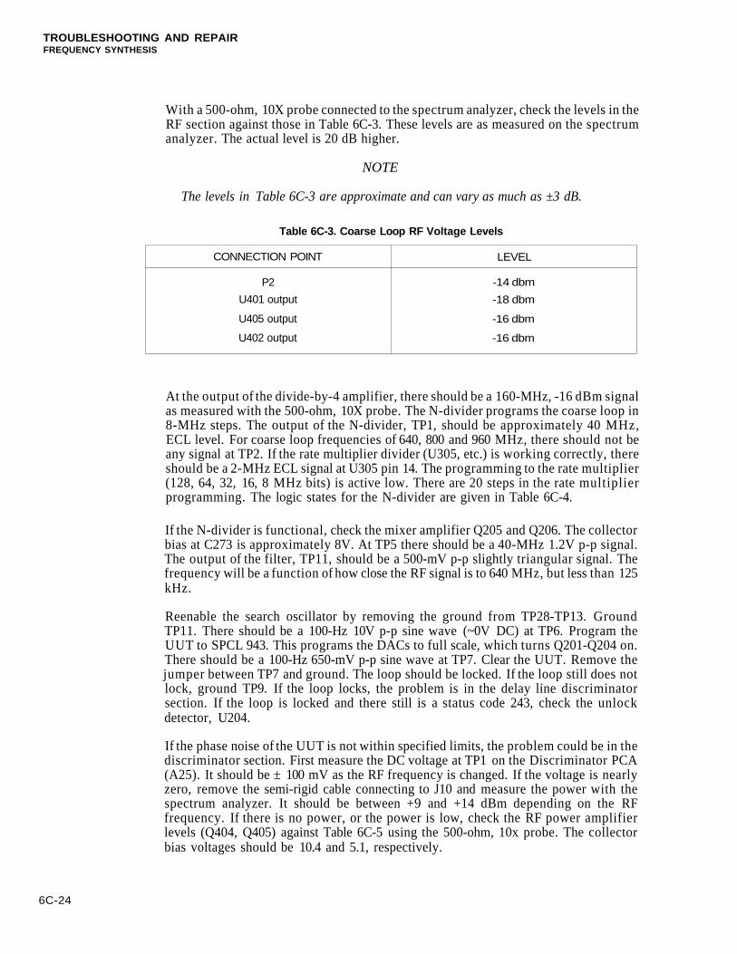
TROUBLESHOOTING AND REPAIRFREQUENCY SYNTHESIS
With a 500-ohm, 10X probe connected to the spectrum analyzer, check the levels in theRF section against those in Table 6C-3. These levels are as measured on the spectrumanalyzer. The actual level is 20 dB higher.
NOTE
The levels in Table 6C-3 are approximate and can vary as much as ±3 dB.
Table 6C-3. Coarse Loop RF Voltage Levels
CONNECTION POINT
P2
U401 output
U405 output
U402 output
LEVEL
-14 dbm
-18 dbm
-16 dbm
-16 dbm
At the output of the divide-by-4 amplifier, there should be a 160-MHz, -16 dBm signalas measured with the 500-ohm, 10X probe. The N-divider programs the coarse loop in8-MHz steps. The output of the N-divider, TP1, should be approximately 40 MHz,ECL level. For coarse loop frequencies of 640, 800 and 960 MHz, there should not beany signal at TP2. If the rate multiplier divider (U305, etc.) is working correctly, thereshould be a 2-MHz ECL signal at U305 pin 14. The programming to the rate multiplier(128, 64, 32, 16, 8 MHz bits) is active low. There are 20 steps in the rate multiplierprogramming. The logic states for the N-divider are given in Table 6C-4.
If the N-divider is functional, check the mixer amplifier Q205 and Q206. The collectorbias at C273 is approximately 8V. At TP5 there should be a 40-MHz 1.2V p-p signal.The output of the filter, TP11, should be a 500-mV p-p slightly triangular signal. Thefrequency will be a function of how close the RF signal is to 640 MHz, but less than 125kHz.
Reenable the search oscillator by removing the ground from TP28-TP13. GroundTP11. There should be a 100-Hz 10V p-p sine wave (~0V DC) at TP6. Program theUUT to SPCL 943. This programs the DACs to full scale, which turns Q201-Q204 on.There should be a 100-Hz 650-mV p-p sine wave at TP7. Clear the UUT. Remove thejumper between TP7 and ground. The loop should be locked. If the loop still does notlock, ground TP9. If the loop locks, the problem is in the delay line discriminatorsection. If the loop is locked and there still is a status code 243, check the unlockdetector, U204.
If the phase noise of the UUT is not within specified limits, the problem could be in thediscriminator section. First measure the DC voltage at TP1 on the Discriminator PCA(A25). It should be ± 100 mV as the RF frequency is changed. If the voltage is nearlyzero, remove the semi-rigid cable connecting to J10 and measure the power with thespectrum analyzer. It should be between +9 and +14 dBm depending on the RFfrequency. If there is no power, or the power is low, check the RF power amplifierlevels (Q404, Q405) against Table 6C-5 using the 500-ohm, 10x probe. The collectorbias voltages should be 10.4 and 5.1, respectively.
6C-24
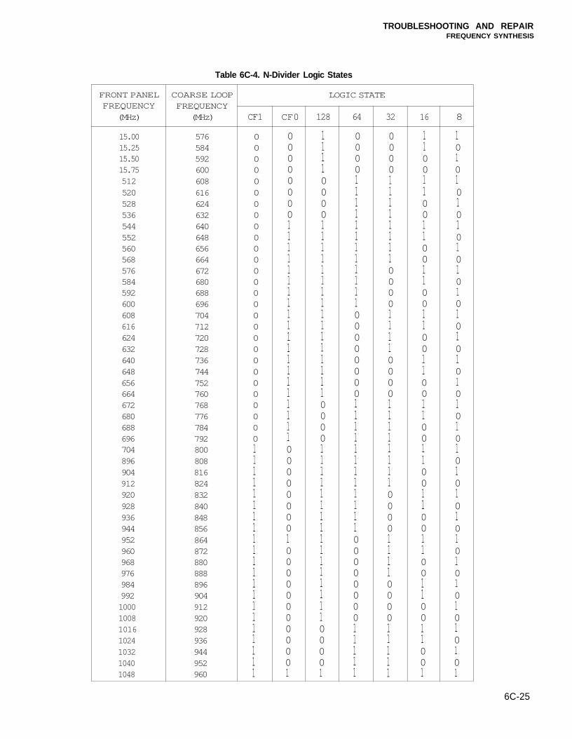
TROUBLESHOOTING AND REPAIRFREQUENCY SYNTHESIS
Table 6C-4. N-Divider Logic States
FRONT PANELFREQUENCY
(MHz)
15.0015.2515.5015.755125205285365445525605685765845926006086166246326406486566646726806886967048969049129209289369449529609689769849921000100810161024103210401048
COARSE LOOPFREQUENCY
(MHz)
576584592600608616624632640648656664672680688696704712720728736744752760768776784792800808816824832840848856864872880888896904912920928936944952960
LOGIC STATE
CF1
0000000000000000000000000000111111111111111111111
CF0
0000000011111111111111111111000000001000000000001
128
1111000011111111111111110000111111111111111100001
64
0000111111111111000000001111111111110000000011111
32
0000111111110000111100001111111100001111000011111
16
1100110011001100110011001100110011001100110011001
8
1010101010101010101010101010101010101010101010101
6C-25
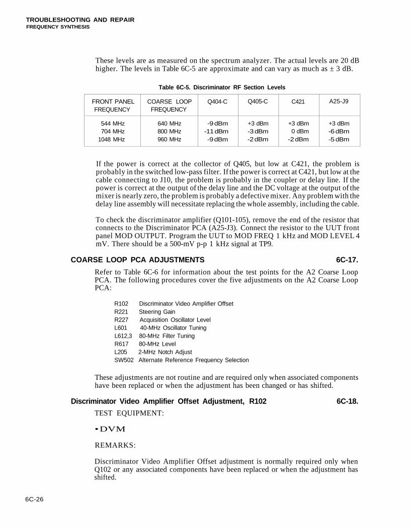
TROUBLESHOOTING AND REPAIRFREQUENCY SYNTHESIS
These levels are as measured on the spectrum analyzer. The actual levels are 20 dBhigher. The levels in Table 6C-5 are approximate and can vary as much as ± 3 dB.
Table 6C-5. Discriminator RF Section Levels
FRONT PANELFREQUENCY
544 MHz704 MHz
1048 MHz
COARSE LOOPFREQUENCY
640 MHz800 MHz960 MHz
Q404-C
-9 dBm-11 dBm-9 dBm
Q405-C
+3 dBm-3 dBm-2 dBm
C421
+3 dBm0 dBm
-2 dBm
A25-J9
+3 dBm-6 dBm-5 dBm
If the power is correct at the collector of Q405, but low at C421, the problem isprobably in the switched low-pass filter. If the power is correct at C421, but low at thecable connecting to J10, the problem is probably in the coupler or delay line. If thepower is correct at the output of the delay line and the DC voltage at the output of themixer is nearly zero, the problem is probably a defective mixer. Any problem with thedelay line assembly will necessitate replacing the whole assembly, including the cable.
To check the discriminator amplifier (Q101-105), remove the end of the resistor thatconnects to the Discriminator PCA (A25-J3). Connect the resistor to the UUT frontpanel MOD OUTPUT. Program the UUT to MOD FREQ 1 kHz and MOD LEVEL 4mV. There should be a 500-mV p-p 1 kHz signal at TP9.
COARSE LOOP PCA ADJUSTMENTS 6C-17.
Refer to Table 6C-6 for information about the test points for the A2 Coarse LoopPCA. The following procedures cover the five adjustments on the A2 Coarse LoopPCA:
R102 Discriminator Video Amplifier OffsetR221 Steering GainR227 Acquisition Oscillator LevelL601 40-MHz Oscillator TuningL612,3 80-MHz Filter TuningR617 80-MHz LevelL205 2-MHz Notch AdjustSW502 Alternate Reference Frequency Selection
These adjustments are not routine and are required only when associated componentshave been replaced or when the adjustment has been changed or has shifted.
Discriminator Video Amplifier Offset Adjustment, R102 6C-18.
TEST EQUIPMENT:
• DVM
REMARKS:
Discriminator Video Amplifier Offset adjustment is normally required only whenQ102 or any associated components have been replaced or when the adjustment hasshifted.
6C-26
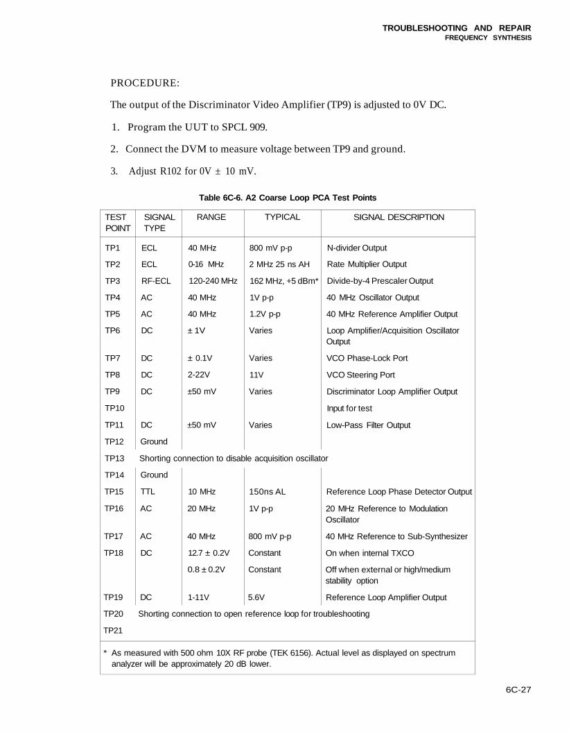
TROUBLESHOOTING AND REPAIRFREQUENCY SYNTHESIS
PROCEDURE:
The output of the Discriminator Video Amplifier (TP9) is adjusted to 0V DC.
1. Program the UUT to SPCL 909.
2. Connect the DVM to measure voltage between TP9 and ground.
3. Adjust R102 for 0V ± 10 mV.
Table 6C-6. A2 Coarse Loop PCA Test Points
TESTPOINT
TP1
TP2
TP3
TP4
TP5
TP6
TP7
TP8
TP9
TP10
TP11
TP12
SIGNALTYPE
ECL
ECL
RF-ECL
AC
AC
DC
DC
DC
DC
DC
Ground
RANGE
40 MHz
0-16 MHz
120-240 MHz
40 MHz
40 MHz
± 1V
± 0.1V
2-22V
±50 mV
±50 mV
TYPICAL
800 mV p-p
2 MHz 25 ns AH
162 MHz, +5 dBm*
1V p-p
1.2V p-p
Varies
Varies
11V
Varies
Varies
SIGNAL DESCRIPTION
N-divider Output
Rate Multiplier Output
Divide-by-4 Prescaler Output
40 MHz Oscillator Output
40 MHz Reference Amplifier Output
Loop Amplifier/Acquisition OscillatorOutput
VCO Phase-Lock Port
VCO Steering Port
Discriminator Loop Amplifier Output
Input for test
Low-Pass Filter Output
TP13 Shorting connection to disable acquisition oscillator
TP14
TP15
TP16
TP17
TP18
TP19
Ground
TTL
AC
AC
DC
DC
10 MHz
20 MHz
40 MHz
12.7 ± 0.2V
0.8 ± 0.2V
1-11V
150ns AL
1V p-p
800 mV p-p
Constant
Constant
5.6V
Reference Loop Phase Detector Output
20 MHz Reference to ModulationOscillator
40 MHz Reference to Sub-Synthesizer
On when internal TXCO
Off when external or high/mediumstability option
Reference Loop Amplifier Output
TP20 Shorting connection to open reference loop for troubleshooting
TP21
* As measured with 500 ohm 10X RF probe (TEK 6156). Actual level as displayed on spectrumanalyzer will be approximately 20 dB lower.
6C-27
TROUBLESHOOTING AND REPAIRFREQUENCY SYNTHESIS
Steering Gain Adjustment, R221 6C-19.
TEST EQUIPMENT:
• DVM
REMARKS:
The Steering Gain Adjustment is normally required only when U207 or any associatedcomponents are replaced or when the adjustment has shifted.
PROCEDURE:
The Coarse Loop VCO steering voltage is adjusted to 24V with the Coarse Loop VCOsteering DAC set to full scale.
1. Program the UUT to SPCL 909.
2. Program the UUT to SPCL 943. This Special Function programs all DACs to fullscale.
3. Connect the DVM to measure the voltage between TP8 and ground (TP14).
4. Adjust R221 for 24.00V ± .01V.
5. Program the UUT for SPCL 00. This clears all Special Functions.
Acquisition Oscillator Level Adjustment, R227 6C-20.
TEST EQUIPMENT:
• DVM
REMARKS:
The Acquisition Oscillator Level adjustment is normally required only when U206 orany associated components have been replaced, or when the adjustment has shifted.
PROCEDURE:
Acquisition Oscillator Level at TP6 is adjusted for 3.54V RMS with the phase lockedloop disabled.
1. Connect TP11 to ground (TP13) with a clip lead.
2. Connect the DVM to measure the AC voltage between TP6 and ground.
3. Adjust R227 for 3.54V RMS ± .1V.
40-MHz Oscillator Adjustment, L601 6C-21.
TEST Equipment:
• Frequency counter• DVM
6C-28
TROUBLESHOOTING AND REPAIRFREQUENCY SYNTHESIS
REMARKS:
The 40-MHz Oscillator Adjustment is normally required only when Q606 or anyassociated components are replaced or when the adjustment has shifted.
PROCEDURE:
The 40-MHz Oscillator is adjusted to 40 MHz with the crystal removed from thecircuit.
1. Program the UUT to SPCL 909 and select internal reference.
2. Connect counter external reference OUT to UUT 10 MHZ IN. Set UUT to EXTREF.
3. Move the two on-board jumpers from TP22-TP24 to TP22-TP23 and fromTP26-TP27 to TP25-TP26. This removes the crystal from the circuit.
4. Connect the frequency counter to TP4. Set for 1-kHz resolution.
5. Adjust L601 for 40 MHz ± 10 kHz.
6. Replace the jumpers to original positions.
7. Set the frequency counter for 1-Hz resolution. Verify the frequency is 40 MHz ± 1count on the frequency counter.
8. Measure voltage at TP19. It should be between 4.5 and 7.5V DC.
80-MHz Filter Tuning, L612 and L613 6C-22.
TEST EQUIPMENT:
• Spectrum analyzer
REMARKS:
The 80-MHz Filter Tuning is normally required only when components in the doublersection have been replaced (Q609, Q610 etc), or when the adjustment has shifted.
PROCEDURE:
The 80-MHz output from the coarse loop is adjusted for maximum.
1. Program the UUT to SPCL 909.
2. Remove the cable and connect the spectrum analyzer to A2-J5. Set the spectrumanalyzer to 80 MHz, 1-MHz span, and 10-dBM reference level.
3. Adjust L612 for maximum level.
4. Adjust L613 for maximum level.
5. Repeat steps 3 and 4 until the level no longer increases.
6. Reinstall the cable.6C-29
TROUBLESHOOTING AND REPAIRFREQUENCY SYNTHESIS
80-MHz Level Adjustment, R617 6C-23.
TEST EQUIPMENT:
• Spectrum analyzer
REMARKS:
The 80-MHz Level Adjustment is normally required only when Q606, Q609, Q610,U601 and associated components have been replaced, or when the adjustment has beenchanged or has shifted. This adjustment should be done after L612 and L613 have beenadjusted.
PROCEDURE:
The 80-MHz Level from A2-J5 is adjusted to 4 dBm.
1. Program UUT to SPCL 909.
2. Remove the cable from A2-J15. Connect A2-J15 to the spectrum analyzer. Set thespectrum analyzer to 80 MHz, 1 MHz-span and 10-dBm reference level.
3. Adjust R617 for 4 dBm ±0.2.
4. Reconnect the cable to A2-J15.
2-MHz Notch Adjustment, L205 6C-24.
TEST EQUIPMENT:
• Spectrum analyzer
REMARKS:
The 2-MHz Notch Adjustment is normally required only if L205 and associatedcomponents have been replaced or when the adjustment has shifted.
PROCEDURE:
The 2-MHz signal, at the output of the acquisition oscillator, is minimized.
1. Program the UUT to SPCL 909.
2. Program the UUT to 15.25 MHz.
3. Connect the spectrum analyzer to TP6 with clip leads. Set the spectrum analyzer tocenter 2 MHz, 100-kHz span, and ref level -20 dB.
4. As L205 is adjusted inward, a signal should be visible on the spectrum analyzer.Adjust L205 to minimize this signal.
6C-30
TROUBLESHOOTING AND REPAIRFREQUENCY SYNTHESIS
Alternate Reference Frequency Selection 6C-25.
REMARKS:
The unit is configured at the factory for 5-MHz external reference when in alternatereference frequency mode, SPCL 761. These are the switch settings for 1- or 2- MHzexternal reference.
PROCEDURE:
On the synthesizer module bottom cover, remove the metal hole plug labeled A2S502.Set the switches as follows:
REFERENCE
5 MHz2 MHz1 MHz
1
onoffoff
2
onoffon
3
offonoff
4
offonon
5
onoffoff
6
offoffon
BAND
123
FREQUENCY RANGE (MHz)
576 - 704712 - 824832 - 968
CSVCO0H
001
CSVCO1H
011
COARSE LOOP VCO (A5) CIRCUIT DESCRIPTION 6C-26.
The A5 Coarse Loop VCO PCA is controlled by the A2 Coarse Loop PCA andproduces a signal that is further processed in the A12 Sum Loop PCA. This assemblyincludes three varactor-tuned oscillator circuits that cover the frequency range 576 to960 MHz, programmed by binary control signals CSVCO0H and CSVCO1H, asfollows:
The three oscillator circuits are of similar design but have different element values andprinted transmission line lengths to cover the three bands. In the following discussion,reference designators for the band 1 oscillator are specified. Corresponding elementsfor the other oscillators are obvious from the schematic.
Each oscillator uses a common-base transistor (Q3) configured for negative resistanceat the emitter. The emitter is coupled to a resonator that consists of a printedtransmission line in series with varactor diodes (CR5, CR6) and low loss porcelaincapacitors (C5, C6). Two tuning voltage lines connect to the varactor cathodes andanodes via RF chokes L6 and L3, respectively. The cathode lines connect to the VCOsteering port, J6. The anode lines connect to the VCO phase lock port, J5. These portsare used by the A2 Coarse Loop PCA to control the operating frequency. The voltageacross the varactors, measured between J6 and J5, varies approximately linearly withfrequency in each band, from about 2V to 20V.
The +13 dBm nominal signal at the oscillator transistor collector is applied to an 8-dBattenuator that provides isolation (R13-R15), and then to a low-pass filter thatattenuates harmonics to less than -20 dBc (C41, C42, and printed lines). PIN diodeCR9 has low RF resistance and passes the oscillator signal when the oscillator is on andgoes to a high impedance when the oscillator is off.
6C-31
TROUBLESHOOTING AND REPAIRFREQUENCY SYNTHESIS
Band control signals CSVCO0H and CSVCO1H are decoded by U3 and Q4-Q8. Thiscircuit applies bias current only to the selected oscillator transistor. Thus, only oneoscillator is activated per band.
PIN diodes CR7-CR9 connect the active oscillator to a resistive signal splitter (R21,R22) that drives monolithic 11 dB amplifiers U1 and U2. The +7 dBm output of U1connects to the A2 Coarse Loop PCA at J7 by a through-the-plate coaxial connector,and the output of U2, also at +7 dBm, connects to the A12 Sum Loop PCA at J8 by acoaxial cable.
COARSE LOOP VCO TROUBLESHOOTING 6C-27.
The Coarse Loop VCO PCA, controlled by the Coarse Loop PCA, generates thecoarse loop signal that is further processed in the Sum Loop PCA. A problem with theCoarse Loop VCO can cause Coarse Loop Unlock status code 243 to appear. Self-testerror codes 320 through 323 can also be triggered by a faulty Sum Loop VCO. Todetermine that the Coarse Loop VCO is faulty, rather than another assembly, thefollowing tests can be performed. First, ground J5, the phase lock port of the VCO witha clip lead. Next, measure the DC voltage at J6 with the UUT programmed to SPCL943 (All DACs to full scale). The reading should be 24.00V. Next, program the UUT toSPCL 942 (All DACs to half scale). The reading should be 12.00V. This tests the VCOsteering voltage circuit.
With J5 still grounded, examine the output at connector J8 with a spectrum analyzer asfrequency is stepped in 8-MHz increments from 512 MHz to 1056 MHz. The frequencyshould always be within about 2 MHz of expected coarse loop frequency, and the levelshould be approximately +5 dBm. Note that the expected coarse loop frequency can bedisplayed by entering SPCL 946. If the signal is good, the problem is likely in anotherPCA. If the signal is faulty only over a frequency band corresponding to one of theVCO bands, the associated VCO circuit is likely at fault. If the VCO appears to befaulty, DC voltages can be measured at various circuit nodes with the UUTprogrammed to frequencies corresponding to the three VCO bands. UUT frequenciesof 600, 700, and 1000 MHz will enable each of the three bands. Refer to Table 6C-7 forexpected approximate voltage measurements. These measurements should help isolatethe faulty circuit.
SUM LOOP BLOCK DIAGRAM 6C-28.
Refer to the Sum Loop Block Diagram (see Figure 6C-8) for help in identifying themajor functional sections and following the signal paths of the sum loop.
Table 6C-7. A5 Coarse Loop VCO PCA Expected DC Voltages
LOCATION
ON bias transistor collector (Q4, Q5, or Q6, depends on band)
OFF bias transistor collectors
ON oscillator transistor collector (Q1, Q2 or Q3, depends on band)
OFF oscillator transistor collectors
U1, U2 outputs
CR7, CR8, CR9 node
VOLTS DC
-14.3
0
+8.3
+9.6
+4.4
+9.9
6C-32
TROUBLESHOOTING AND REPAIRFREQUENCY SYNTHESIS
6C-33
Figure 6C-8. Sum Loop Block Diagram
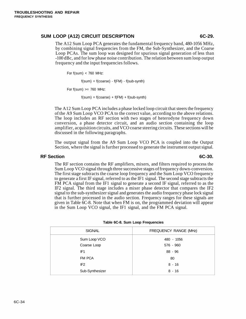
TROUBLESHOOTING AND REPAIRFREQUENCY SYNTHESIS
SUM LOOP (A12) CIRCUIT DESCRIPTION 6C-29.
The A12 Sum Loop PCA generates the fundamental frequency band, 480-1056 MHz,by combining signal frequencies from the FM, the Sub-Synthesizer, and the CoarseLoop PCAs. The sum loop was designed for spurious signal generation of less than-100 dBc, and for low phase noise contribution. The relation between sum loop outputfrequency and the input frequencies follows.
For f(sum) < 760 MHz:
f(sum) = f(coarse) - f(FM) - f(sub-synth)
For f(sum) >= 760 MHz:
f(sum) = f(coarse) + f(FM) + f(sub-synth)
The A12 Sum Loop PCA includes a phase locked loop circuit that steers the frequencyof the A9 Sum Loop VCO PCA to the correct value, according to the above relations.The loop includes an RF section with two stages of heterodyne frequency downconversion, a phase detector circuit, and an audio section containing the loopamplifier, acquisition circuits, and VCO coarse steering circuits. These sections will bediscussed in the following paragraphs.
The output signal from the A9 Sum Loop VCO PCA is coupled into the OutputSection, where the signal is further processed to generate the instrument output signal.
RF Section 6C-30.
The RF section contains the RF amplifiers, mixers, and filters required to process theSum Loop VCO signal through three successive stages of frequency down-conversion.The first stage subtracts the coarse loop frequency and the Sum Loop VCO frequencyto generate a first IF signal, referred to as the IF1 signal. The second stage subtracts theFM PCA signal from the IF1 signal to generate a second IF signal, referred to as theIF2 signal. The third stage includes a mixer phase detector that compares the IF2signal to the sub-synthesizer signal and generates the audio frequency phase lock signalthat is further processed in the audio section. Frequency ranges for these signals aregiven in Table 6C-8. Note that when FM is on, the programmed deviation will appearin the Sum Loop VCO signal, the IF1 signal, and the FM PCA signal.
Table 6C-8. Sum Loop Frequencies
6C-34
SIGNAL
Sum Loop VCO
Coarse Loop
IF1
FM PCA
IF2
Sub-Synthesizer
FREQUENCY RANGE (MHz)
480 - 1056
576 - 960
88 - 96
80
8 - 16
8 - 16
TROUBLESHOOTING AND REPAIRFREQUENCY SYNTHESIS
The Sum Loop VCO signal at J9 is applied to buffer amplifiers U7 and U8. PIN diodeCR4 follows U8 and acts as an adjustable attenuator to control the level at the RF portof double balanced mixer U1. A low-pass filter including C81 and C82 precedes U1 RFport and attenuates high order harmonics in the RF signal. The LO port of U1 is drivenby a two-stage amplifier that includes Q1 and Q2. This amplifier accepts the +7 dBmsignal from the Coarse Loop VCO at J11 and produces +20 dBm of drive power at theLO port of U1.
U1 generates the IF1 signal at the IF port. This signal is filtered by a 10-element,100-MHz low-pass filter with input at L3 and output at C27. The filter is containedwithin a channel in an aluminum cover piece that improves high frequencyattenuation. This cover also shields the IF1 amplifiers and the IF2 low-pass filter. The-14-dBm IF1 signal at the filter output is amplified by Q5, configured for 21-dB gain.Q5 drives level detector diode CR1 at +7 dBm. CR1, U4 and associated componentsform a level control loop that holds RF level constant at CR1 by adjusting modulatorPIN diode CR4 bias current. This action also holds the signal level at U1 RF port to aconstant value. Accurate RF port level control is necessary to control mixer intermodspurs and noise floor. The leveled IF1 signal at CR1 is next applied to a 6-dBattenuator (R25-27) and then to Q6, which is configured as a 20-dB amplifier. Q6drives the LO port of double balanced mixer U2 with about +20 dBm. The 80-MHzsignal from the A14 FM PCA is applied to the RF port of U2. This signal is coupled viaa capacitor at J17. Q8 and associated components buffer and low-pass filter this signal,which is then applied to U2 at a level of -8 dBm.
U2 generates the IF2 signal at the IF port. This signal is filtered by a nine-element,20-MHz low-pass filter with input at L9 and output at L23. Like the IF1 filter, thisfilter is contained within a channel in an aluminum cover piece that improves highfrequency attenuation. The -14 dBm signal at the filter output drives the IF2 amplifier,which includes Q9 and Q10 and is configured for 21 dB gain. Q10 drives the RF port ofmixer U3 with +7 dBm, which is used as a phase detector. The IF2 low-pass filter alsoprovides a DC path for +15V power for the IF2 amplifier.
The LO port of phase detector U3 is driven by a signal derived from theSub-Synthesizer PCA, as follows. J10 is connected to the 16- to 32-MHz signal fromthe A3 Sub-Synthesizer PCA. This ECL level signal is converted to TTL by Q11 andrelated parts. The TTL signal then drives U5, a D type flip-flop that is configured tohalve the input frequency. The resulting 8-to 16-MHz Q and Q (compliment) outputsof U5 drive the LO port of U3. The IF output of U3 drives the loop filter, a 13-elementlow-pass type with input at R56 and output at L26. This filter allows audio frequencycomponents to pass with minimum phase shift while adequately attenuating RF mixerproducts. The loop filter output voltage is proportional to the phase differencebetween the RF and LO ports of U3. This signal drives the Audio Section, which isdescribed in the following paragraphs.
Audio Section 6C-31.
The Audio Section contains the circuits required to acquire and maintain phase lock.Inputs to this section include the phase detector voltage, Sum Loop VCO coarsesteering voltage (SUMSTEER), FM modulation signal (SUMAUDIO), FM rangeswitching signals (SUMVCO4-6), and Sum Loop VCO Kv information(SUMCOMPHO-7). Audio Section outputs include Sum Loop VCO steering port andphase lock port voltages, and a phase lock status indicator for the controller. Thesecircuits are described in the following paragraphs.
6C-35
TROUBLESHOOTING AND REPAIRFREQUENCY SYNTHESIS
LOOP AMPLIFIER
The loop amplifier consists of a low frequency path and a high frequency pathconnected in parallel, and is driven by the phase detector voltage at the loop filteroutput (L26). This configuration was chosen to minimize noise and phase shift atfrequencies around the unity loop gain frequency of 500 kHz.
The low frequency path is operative from DC to about 30 kHz, and includes OPAMPS U104, U105, and associated components. U105 is also configured to act as aWien bridge type acquisition oscillator. When the sum loop is unlocked, U105oscillates at either 800 Hz or 14 kHz, depending on switching FETs Q106-107, whichswitch capacitors C127 and C131. Potentiometer R132 sets the amplitude ofoscillation. U105 stops oscillating and acts as a gain-of-3 amplifier when phase lock isobtained, due to loop dynamics.
The high frequency path is operative for frequencies greater than about 30 kHz, andincludes Q108 and associated components. Q108 is a low noise, high ft transistorconfigured as an emitter follower. An R-C circuit sums the outputs of the two paths,with C137 and C138 providing high-pass and low-pass characteristics, respectively.Loop gain adjustment is provided by R167.
The summing node, at TP4, is connected to the sum loop VCO phase lock port, J6. Sixswitchable resistors, R138-143, also connect this node to ground. These switchedresistors are used to adjust loop amplifier gain to compensate for sum loop VCO Kvvariations. Note that Kv is the slope of the frequency vs. tuning voltage function. Theswitched resistors are programmed by U110, a PROM that contains a look-up table.SUMCOMP bits 0-7, a binary number proportional to 1 / Kv, is the input to U110. Thesix-bit output of U110, functionally related to the SUMCOMP number, drives theprogrammed resistors in a way to compensate for Kv variation with sum loop VCO RFfrequency.
ACQUISITION CIRCUITS
The acquisition circuit includes several parts, including a two frequency acquisitionoscillator, an unlock detecting comparator, a loop disabling circuit, and a dualmonostable multivibrator. These parts interact as described below.
When the loop is properly phase locked, the phase detector voltage at TP5 stays closeto 0V, because the loop forces equal frequency and nearly equal phase for the phasedetector inputs. If the loop was opened, for instance by shorting the VCO phase lockport at TP4, the phase detector would generate a beat frequency triangle wave signal ofabout 300 mV amplitude. Thus, the presence of a voltage above a threshold levelindicates loop unlock. High speed comparator U115 trips and activates a two-stageacquisition sequence when the phase detector voltage exceeds 190 mV, indicating loopunlock.
The output of U115 is applied to the 1A input of U114, a dual monostablemultivibrator, and trips the A one-shot upon unlock detection. One-shot A isconfigured for a 10 ms output pulse, and drives comparators U102A and U102B, whichdisable the low and high frequency paths of the loop amplifier, respectively, during the10 ms pulse. U102A turns off Q109, and U102B turns off bias current to Q108,effectively open circuiting the loop amplifier. This disabling action opens the loop andallows time for all the frequency inputs to the Sum Loop PCA to settle to proper valuesfollowing a change in instrument RF frequency, prior to sum loop phase lock
6C-36
TROUBLESHOOTING AND REPAIRFREQUENCY SYNTHESIS
acquisition. The trailing edge of the one-shot A pulse triggers one-shot B, at the 2Binput. One-shot B is configured for a 0.5 ms pulse and drives comparator U102C,which switches acquisition oscillator U105 to the 14-kHz mode. This acquisitionfrequency results in optimum lock-on behavior. During the 0.5-ms pulse, unlockcomparator U115 is disabled, to allow acquisition to occur. If Sum Loop PCA inputsare correct, acquisition occurs during the 0.5 ms pulse, and U105 stops oscillating, dueto changes in loop dynamics. After the 0.5-ms one-shot B pulse, U105 is set to the800-Hz mode to improve closed-loop dynamics, but doesn't oscillate if the lock wasobtained.
U102D is a zero crossing comparator that senses the polarity at TP1, the low frequencyloop amplifier output, and generates the SUMVOLH signal. The controller uses thissignal during the sum loop VCO calibration routine.
U116 is a monostable multivibrator that is triggered by the acquisition oscillation atU105 that occurs when the sum loop is unlocked, and generates the SUMUNLKLsignal. This informs the controller that the sum loop is not locked.
SUM LOOP VCO STEERING CIRCUIT
The Sum Loop VCO has two ports for frequency tuning, the steering port at J5 and thephase-lock-port at J6. A coarse tuning voltage, generated at the steering port, tunes theSum Loop VCO frequency to the desired value, within about ± 2 MHz. The phase lockport is driven by the loop amplifier with enough voltage to compensate for the error inthe steering port and sets the Sum Loop VCO frequency to the correct phase-lockedvalue. The following paragraphs describe the circuit that drives the steering port.
The SUMSTEER signal at J7-14 is an RF frequency dependent DC voltage that isproportional to the required Sum Loop VCO steering port voltage. This signal isgenerated in a 12-bit DAC on the A11 Modulation Control PCA that is programmedby data stored in the controller. Note that this data is obtained and stored during theSum Loop VCO compensation procedure, and is unique to a given VCO. TheSUMSTEER signal is low-pass filtered and amplified by U103 and associatedcomponents. Gain adjustment is provided by R112. The DC voltage at the steeringport, TP3, varies from 0 to 26V, depending on RF frequency.
The source of FM in the signal generator is the 80-MHz signal from the A14 FM PCA,an input to the sum loop. Since the Sum Loop VCO is phase locked to this signal, anyfrequency modulation on the 80-MHz FM PCA signal is transferred to the Sum LoopVCO. However, at high levels of FM deviation, the required voltage swing at the VCOphase lock port would require a phase detector output greater than possible, and thusthe Sum Loop would lose lock. This problem is avoided by applying an AC signal atthe VCO steering port that provides nearly the correct deviation in the Sum LoopVCO, during high deviation FM operation. Thus, the loop must only generate a smallerror voltage at the VCO phase lock port to maintain lock, and the phase detectoroutput stays acceptably small.
The SUMAUDIO signal at J8-1 is from the A14 FM PCA and is an AC frequencymodulating signal with amplitude proportional to FM deviation. This signal isbuffered by OP AMP U106, which is configured for unity gain and can be switched viaU107 for inverting or non-inverting operation. These two modes are required toproperly phase the cancellation signal, depending on fundamental frequency band.For f(fund) < 760 MHz, U106 inverts, while for f(fund) >= 760 MHz, U106 isnon-inverting. Gain equalization for the two modes is provided by R121. The buffered
6C-37
TROUBLESHOOTING AND REPAIRFREQUENCY SYNTHESIS
signal at TP2 is next applied to DAC U109, which is programmed by SUMCOMP bits0-7. These 8 bits encode a number proportional to Sum Loop VCO 1 / Kv. Note that Kvis the slope of the frequency vs. tuning voltage function. Thus, DAC U109 scales thesignal to account for VCO tuning voltage sensitivity variations with RF frequency.Gain adjustment for DAC U109 is provided by R116. The DAC output at U108 pin 6 isnext applied to a switched R-C network including R105-108 and related components,that is programmed by FM range switching bits SUMVCO4-6 depending on FMdeviation range. This network scales the signal to the appropriate level. The output ofthe network, at TP3, the VCO steering port, is the desired AC cancellation signal.Noise contribution at the VCO steering port is reduced by C105, which is switched toground by Q101 when the cancellation circuit is not active.
SUM LOOP TROUBLESHOOTING 6C-32.
Since the primary function of the sum loop is to combine various signal frequenciesinto the desired fundamental band frequency, sum loop problems will generally causefrequency errors at the UUT output. A first step in troubleshooting is to check for sumloop fault status codes 244 and 245. The implications and suggested troubleshootingsequence in response to these codes are described below. Reading and understandingthe detailed circuit descriptions for the sum loop and Sum Loop VCO assemblies(paragraphs 6C-28 through 6C-31 and 6C-39) is highly recommended prior totroubleshooting.
Status code 244 indicates that the sum loop is not properly phase locked, and istriggered by the free running loop acquisition oscillator. This fault condition can becaused by either a problem with the input signals to the sum loop, or by a problem inthe A12 Sum Loop PCA or the A9 Sum Loop VCO PCA. A faulty input signal fromeither the Coarse Loop, the Sub-Synthesizer, or the FM assembly could result in sumloop unlock.
First, check for status codes that indicate faulty operation of the Sub-SynthesizerPCA, the Coarse Loop PCA, and the FM PCA. Repair any indicated assemblies andcheck whether Status Code 244 still appears. If it does, check that the following threeinput signals have the correct frequency and level. The FM signal is measured using a500-ohm probe with the spectrum analyzer, while the coarse loop and sub-synthesizercables are detached from the Sum Loop PCA and are connected to the spectrumanalyzer directly. Note that for any UUT frequency, the expected coarse loop andsub-synthesizer frequencies can be displayed by entering SPCL 946 and SPCL 947,respectively.
SIGNAL DESCRIPTION
Coarse Loop
FM
Sub-Synthesizer
TEST LOCATION
Cable W14
TP14
Cable W13
FREQUENCY
Use SPCL 946
80 Mhz
See equations below
Or, use SPCL 947
LEVEL
+7 dBm
-13 dBm
+3 dBm
For f(sum) < 760 Mhz, f in Mhz:
f(sub-synth) = 2*(f(coarse) -80 -f(sum))
For f(sum) >= 760 Mhz, f in Mhz:
f(sub-synth) = 2*(f(sum) -80 -f(coarse))
6C-38
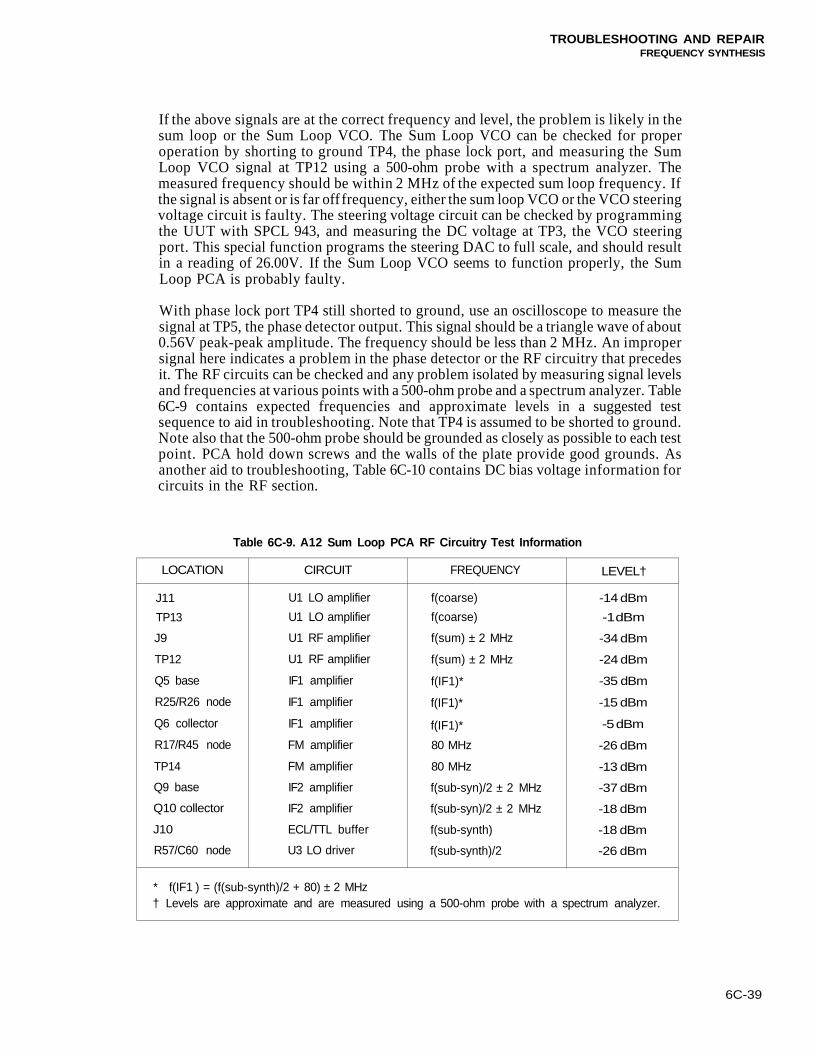
TROUBLESHOOTING AND REPAIRFREQUENCY SYNTHESIS
If the above signals are at the correct frequency and level, the problem is likely in thesum loop or the Sum Loop VCO. The Sum Loop VCO can be checked for properoperation by shorting to ground TP4, the phase lock port, and measuring the SumLoop VCO signal at TP12 using a 500-ohm probe with a spectrum analyzer. Themeasured frequency should be within 2 MHz of the expected sum loop frequency. Ifthe signal is absent or is far off frequency, either the sum loop VCO or the VCO steeringvoltage circuit is faulty. The steering voltage circuit can be checked by programmingthe UUT with SPCL 943, and measuring the DC voltage at TP3, the VCO steeringport. This special function programs the steering DAC to full scale, and should resultin a reading of 26.00V. If the Sum Loop VCO seems to function properly, the SumLoop PCA is probably faulty.
With phase lock port TP4 still shorted to ground, use an oscilloscope to measure thesignal at TP5, the phase detector output. This signal should be a triangle wave of about0.56V peak-peak amplitude. The frequency should be less than 2 MHz. An impropersignal here indicates a problem in the phase detector or the RF circuitry that precedesit. The RF circuits can be checked and any problem isolated by measuring signal levelsand frequencies at various points with a 500-ohm probe and a spectrum analyzer. Table6C-9 contains expected frequencies and approximate levels in a suggested testsequence to aid in troubleshooting. Note that TP4 is assumed to be shorted to ground.Note also that the 500-ohm probe should be grounded as closely as possible to each testpoint. PCA hold down screws and the walls of the plate provide good grounds. Asanother aid to troubleshooting, Table 6C-10 contains DC bias voltage information forcircuits in the RF section.
Table 6C-9. A12 Sum Loop PCA RF Circuitry Test Information
LOCATION
J11
TP13
J9
TP12
Q5 base
R25/R26 node
Q6 collector
R17/R45 node
TP14
Q9 base
Q10 collector
J10
R57/C60 node
CIRCUIT
U1 LO amplifier
U1 LO amplifier
U1 RF amplifier
U1 RF amplifier
IF1 amplifier
IF1 amplifier
IF1 amplifier
FM amplifier
FM amplifier
IF2 amplifier
IF2 amplifier
ECL/TTL buffer
U3 LO driver
FREQUENCY
f(coarse)
f(coarse)
f(sum) ± 2 MHz
f(sum) ± 2 MHz
f(IF1)*
f(IF1)*
f(IF1)*
80 MHz
80 MHz
f(sub-syn)/2 ± 2 MHz
f(sub-syn)/2 ± 2 MHz
f(sub-synth)
f(sub-synth)/2
LEVEL†
-14 dBm
-1 dBm
-34 dBm
-24 dBm
-35 dBm
-15 dBm
-5 dBm
-26 dBm
-13 dBm
-37 dBm
-18 dBm
-18 dBm
-26 dBm
* f(IF1 ) = (f(sub-synth)/2 + 80) ± 2 MHz† Levels are approximate and are measured using a 500-ohm probe with a spectrum analyzer.
6C-39
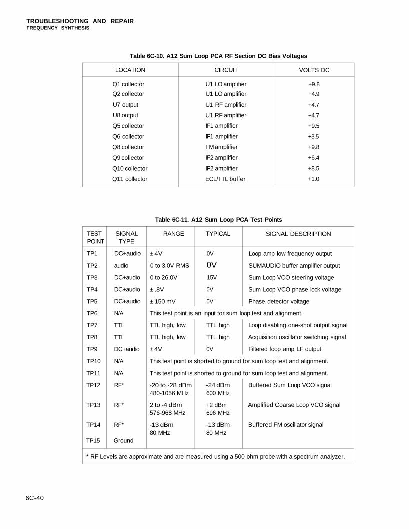
TROUBLESHOOTING AND REPAIRFREQUENCY SYNTHESIS
Table 6C-10. A12 Sum Loop PCA RF Section DC Bias Voltages
Table 6C-11. A12 Sum Loop PCA Test Points
6C-40
LOCATION
Q1 collector
Q2 collector
U7 output
U8 output
Q5 collector
Q6 collector
Q8 collector
Q9 collector
Q10 collector
Q11 collector
CIRCUIT
U1 LO amplifier
U1 LO amplifier
U1 RF amplifier
U1 RF amplifier
IF1 amplifier
IF1 amplifier
FM amplifier
IF2 amplifier
IF2 amplifier
ECL/TTL buffer
VOLTS DC
+9.8
+4.9
+4.7
+4.7
+9.5
+3.5
+9.8
+6.4
+8.5
+1.0
TESTPOINT
TP1
TP2
TP3
TP4
TP5
TP6
TP7
TP8
TP9
TP10
TP11
TP12
TP13
TP14
TP15
SIGNALTYPE
DC+audio
audio
DC+audio
DC+audio
DC+audio
N/A
TTL
TTL
DC+audio
N/A
N/A
RF*
RF*
RF*
Ground
RANGE
± 4V
0 to 3.0V RMS
0 to 26.0V
± .8V
± 150 mV
TYPICAL
0V
0V15V
0V
0V
SIGNAL DESCRIPTION
Loop amp low frequency output
SUMAUDIO buffer amplifier output
Sum Loop VCO steering voltage
Sum Loop VCO phase lock voltage
Phase detector voltage
This test point is an input for sum loop test and alignment.
TTL high, low
TTL high, low
± 4V
TTL high
TTL high
0V
Loop disabling one-shot output signal
Acquisition oscillator switching signal
Filtered loop amp LF output
This test point is shorted to ground for sum loop test and alignment.
This test point is shorted to ground for sum loop test and alignment.
-20 to -28 dBm480-1056 MHz
2 to -4 dBm576-968 MHz
-13 dBm80 MHz
-24 dBm600 MHz
+2 dBm696 MHz
-13 dBm80 MHz
Buffered Sum Loop VCO signal
Amplified Coarse Loop VCO signal
Buffered FM oscillator signal
* RF Levels are approximate and are measured using a 500-ohm probe with a spectrum analyzer.
TROUBLESHOOTING AND REPAIRFREQUENCY SYNTHESIS
A proper signal at TP5, with TP4 shorted to ground, indicates that the RF circuits areprobably not faulty, and that the problem is in the audio section. The loopamplifier/acquisition oscillator can be checked by shorting TP5 to ground andmeasuring the waveform at TP1 with an oscilloscope, which should be a sine wave ofabout 800 Hz and 14V pk-pk level. Next, measure the TP1 waveform with both TP5and TP8 shorted to ground. The waveform should be a sine wave of about 13.6 kHzand 8V pk-pk level. Failure of this test indicates a problem somewhere between TP5and TP1.
The programmable attenuator can be checked for proper operation as follows. First,connect test points 7 and 9 to ground, and program the UUT to SPCL 943 (DACs setto full scale). Measure the resistance from TP4 to ground. The reading should be about240 ohms. Next, program the UUT to SPCL 941 (DACs set to zero). The resistancereading should now be about 29.5 ohms. Failure of this test indicates a problemsomewhere between TP1 and TP4.
Status Code 245 indicates an unleveled condition in the leveling loop that controls thesignal amplitude at the RF input of mixer U1, and is triggered when the modulatorcontrol voltage at Jl6 exceeds about 10V. This fault condition can be caused by either alevel problem in the RF path including the Sum Loop VCO and sum loop circuitsbetween J9 and CR1, or by improper signal frequencies within the sum loop.
Table 6C-11 presents the nominal characteristics of the signals at the various test pointson the A12 Sum Loop PCA. The normal range of the signals, along with specific valuesfor the instrument diagnostic state, SPCL 909, are listed.
SUM LOOP ASSEMBLY ADJUSTMENTS 6C-33.
The following procedures cover the five potentiometer adjustments on the A12 SumLoop PCA listed below:
R112, Steering LevelR121, Buffer Gain MatchR116, FM NullR167, Loop GainR132, Acquisition Oscillator Level
NOTE
These adjustments are not routine and are required only when associatedcomponents have been replaced or when the adjustment has beenchanged.
Steering Level Adjustment, R112 6C-34.
TEST EQUIPMENT:
• DVM
REMARKS:
The Steering Level Adjustment is normally required only when U103 or any associatedcomponents are replaced or when the adjustment has shifted.
6C-41
TROUBLESHOOTING AND REPAIRFREQUENCY SYNTHESIS
PROCEDURE:
The Sum Loop VCO steering voltage is adjusted to +26V DC with the Sum Loop VCOsteering DAC set to full scale.
1. Program the UUT to SPCL 909.
2. Program the UUT to SPCL 943. This special function programs all DACs to fullscale.
3. Connect the DVM to measure the voltage between TP3 and TP15 (ground).
4. Adjust R112 for +26.00V ± .02V.
5. Program the UUT for SPCL 00. This clears all Special Functions.
Buffer Gain Match Adjustment, R121 6C-35.
TEST EQUIPMENT:
• DVM
REMARKS:
The buffer gain match adjustment is normally required only when U106 or anyassociated components are replaced or when the adjustment has shifted.
PROCEDURE:
The SUMAUDIO buffer amplifier is adjusted for equal gain in the inverting andnon-inverting modes.
1. Program the UUT to SPCL 909, 800 MHz, 4-MHz FM deviation, and 1-kHz modfrequency. Turn INT FM on.
2. Connect the DVM to measure the AC voltage between TP2 and TP15 (ground).
3. Note the DVM reading.
4. Program the UUT to 700 MHz.
5. Adjust R121 for a DVM reading equal to that noted in step 3, ± 5 mV.
FM Null Adjustment, R116 6C-36.
TEST EQUIPMENT:
• Oscilloscope
REMARKS:
The FM null adjustment is required under the following conditions:
• The A12 Sum Loop PCA has been replaced or the A14 FM PCA has been replacedor repaired.
6C-42
TROUBLESHOOTING AND REPAIRFREQUENCY SYNTHESIS
• U108, U109, or any associated components are replaced or the adjustment hasbeen changed or has shifted.
PROCEDURE:
The AC error voltage at TP5, the phase-detector output, is adjusted for a minimumpeak-to-peak value with the UUT programmed for INT FM on, with 4-MHz FMdeviation at 168-kHz mod frequency.
1. Program the UUT to SPCL 909, 700 MHz, 4-MHz deviation, and 168-kHz modfrequency. Turn INT FM on.
2. Set the oscilloscope for 50 mV/division vertical, 2 us/division horizontal, and ACcoupling.
3. Connect the oscilloscope probe to monitor the signal at TP5, using TP15 for theground connection.
4. Adjust R116 for a minimum peak-to-peak voltage. The waveform should be lessthan 150 mV peak-to-peak.
Loop Gain Adjustment, R167 6C-37.
TEST EQUIPMENT:
• Low frequency synthesized signal generator (LFSSG) Wideband AC voltmeter(WBVM)
REMARKS:
• The Loop Gain Adjustment is normally required only when U3, Q108, or anyassociated components are replaced or when the adjustment has shifted.
• The upper plate cover of the lower module must be installed prior to thisadjustment.
PROCEDURE:
An 800-kHz AC signal is applied to the Sum Loop VCO steering port through TP6.Loop gain is adjusted via R167 so that the AC voltages at the Sum Loop VCO steeringand phase lock ports are equal.
1. Access R167, TP3, TP4, and TP6 by removing the appropriate plate cover accessplugs.
2. Program the UUT to SPCL 909, 548 MHz, 150-kHz FM deviation. Turn EXT ACFM on.
3. Program the LFSSG to 800 kHz, 20 mV RMS.
4. Connect the LFSSG output to TP6 via a BNC to clip lead adapter. Connect theground clip to the plate cover adjacent to TP6.
6C-43
TROUBLESHOOTING AND REPAIRFREQUENCY SYNTHESIS
5. Connect the WBVM to measure the AC voltage between TP3 and the plate coveradjacent to TP3 (ground).
6. Program the WBVM for dB relative. The reading should be 0 dB.
7. Connect the WBVM to measure the AC voltage between TP4 and the plate cover.
8. Adjust R167 for an indication of 0.0 dB ± .1 dB.
9. Replace the access plugs.
Acquisition Oscillator Level Adjustment, R132 6C-38.
TEST EQUIPMENT:
• DVM
REMARKS:
The acquisition oscillator level adjustment is normally required only when U105 or anyassociated components are replaced or when the adjustment has been changed or hasshifted.
PROCEDURE:
Acquisition oscillator level at TP1 is adjusted for 2.82V RMS with the phase lockedloop disabled.
1. Connect TP5 to TP15 with a clip lead. Connect TP8 to TP15 with a clip lead.
2. Connect the DVM to measure the AC voltage between TP1 and TP15 (ground).
3. Adjust R132 for an indication of 2.83V RMS ± .05V.
SUM LOOP VCO (A9) CIRCUIT DESCRIPTION 6C-39.
The A9 Sum Loop VCO PCA is controlled by the A12 Sum Loop PCA and producesthe fundamental band signal that is further processed in the Output Section to becomethe signal generator output. This assembly includes four varactor-tuned oscillatorcircuits that cover the frequency range 480 MHz to 1056 MHz, programmed by binarycontrol signals SUMVCO0H and SUMVCO1H, as follows:
The four oscillator circuits are of similar design, but with different element values andprinted transmission line lengths to cover the four bands. In the following discussion,reference designators for the band 1 oscillator will be specified. Correspondingelements for the other oscillators are obvious from the schematic.
6C-44
BAND
1234
FREQUENCY RANGE (MHz)
480-624.999999625-759.999999760-894.999999895-1056
SUMVCO0H
0011
SUMVC01H
1001
TROUBLESHOOTING AND REPAIRFREQUENCY SYNTHESIS
Each oscillator uses a common-base transistor (Q4) configured for negative resistanceat the emitter. The emitter is coupled to a resonator that consists of a printedtransmission line in series with varactor diodes (CR7, CR8) and low loss porcelaincapacitors (C7, C8). Two tuning voltage lines connect to the varactor cathodes andanodes via RF chokes L8 and L4, respectively. The cathode lines connect to the VCOsteering port, J5. The anode lines connect to the VCO phase lock port, J6. These portsare used by the A12 Sum Loop PCA to control the operating frequency. The voltageacross the varactors, measured between J6 and J5, varies approximately linearly withfrequency in each band, from about +2V to +20V.
The +13 dBm nominal signal at the oscillator transistor collector is applied to an 8-dBattenuator that provides isolation (R18-R20), and then to a low-pass filter thatattenuates harmonics to less than -20 dBc (C51, C52 and printed lines). PIN diodeCR12 has low RF resistance and passes the oscillator signal when the oscillator is on,and goes to a high impedance when the oscillator is off.
Band control signals SUMVCO0H and SUMVCO1H are decoded by U5 and Q5-Q10.This circuit applies bias current only to the selected oscillator transistor. Thus, onlyone oscillator is activated per band.
PIN diodes CR9-CR12 connect the active oscillator to a resistive signal splitter (R22,R23, R50). One signal splitter output goes to series-connected monolithic 11-dBamplifiers U1 and U2. A -12 dB pad (R26-R28) is between U1 and U2. Two amplifiersare required for adequate isolation between the Sum Loop and the Premodulatorassemblies. The output of U2, at about +7 dBm, is connected to the A10 PremodulatorPCA by a plug in capacitor at J7.
The other signal splitter output goes to an identically configured circuit includingamplifiers U3 and U4. Following U4 is a low pass filter including C69 and C70 thatattenuates high frequency harmonics. The filtered output from U4 is connected to theA12 Sum Loop PCA at P1 by a through-the-plate composition resistor. Thiscomponent behaves as a distributed RC lowpass filter at very high frequencies, andimproves sum loop spurious performance.
SUM LOOP VCO TROUBLESHOOTING 6C-40.
The Sum Loop VCO PCA, along with the Sum Loop PCA, generates the fundamentalfrequency band. A problem with the Sum Loop VCO can cause Sum Loop Unlockstatus code 244 or Sum Loop Unlevel status code 245 to appear. Self-Test error codes327 through 333 can also be triggered by a faulty Sum Loop VCO. To determine thatthe Sum Loop VCO is faulty, rather than another assembly, the following tests can beperformed.
1. Ground the phase lock port of the VCO with a clip lead (J6, Sum Loop VCO orTP4, Sum Loop).
2. Measure the DC voltage at J5 with the signal generator programmed to SPCL 943(All DACs to full scale).
The reading should be +26.00V.
3. Program the UUT to SPCL 942 (All DACs to half scale).
The reading should be +13.00V. This tests the VCO steering voltage circuit.
6C-45
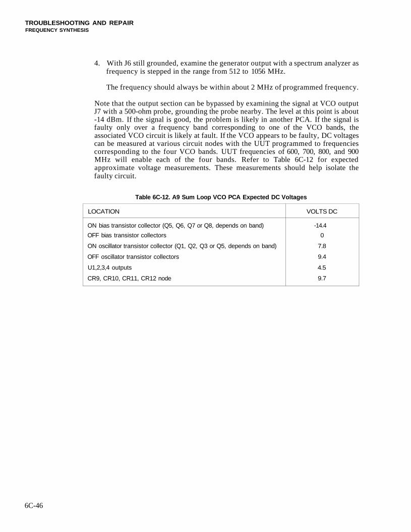
TROUBLESHOOTING AND REPAIRFREQUENCY SYNTHESIS
4. With J6 still grounded, examine the generator output with a spectrum analyzer asfrequency is stepped in the range from 512 to 1056 MHz.
The frequency should always be within about 2 MHz of programmed frequency.
Note that the output section can be bypassed by examining the signal at VCO outputJ7 with a 500-ohm probe, grounding the probe nearby. The level at this point is about-14 dBm. If the signal is good, the problem is likely in another PCA. If the signal isfaulty only over a frequency band corresponding to one of the VCO bands, theassociated VCO circuit is likely at fault. If the VCO appears to be faulty, DC voltagescan be measured at various circuit nodes with the UUT programmed to frequenciescorresponding to the four VCO bands. UUT frequencies of 600, 700, 800, and 900MHz will enable each of the four bands. Refer to Table 6C-12 for expectedapproximate voltage measurements. These measurements should help isolate thefaulty circuit.
Table 6C-12. A9 Sum Loop VCO PCA Expected DC Voltages
LOCATION
ON bias transistor collector (Q5, Q6, Q7 or Q8, depends on band)
OFF bias transistor collectors
ON oscillator transistor collector (Q1, Q2, Q3 or Q5, depends on band)
OFF oscillator transistor collectors
U1,2,3,4 outputs
CR9, CR10, CR11, CR12 node
VOLTS DC
-14.4
0
7.8
9.4
4.5
9.7
6C-46
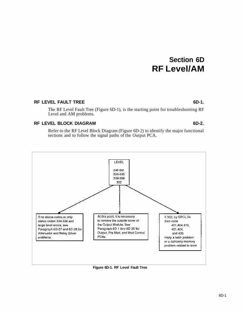
Section 6DRF Level/AM
RF LEVEL FAULT TREE 6D-1.
The RF Level Fault Tree (Figure 6D-1), is the starting point for troubleshooting RFLevel and AM problems.
RF LEVEL BLOCK DIAGRAM 6D-2.
Refer to the RF Level Block Diagram (Figure 6D-2) to identify the major functionalsections and to follow the signal paths of the Output PCA.
Figure 6D-1. RF Level Fault Tree
6D-1
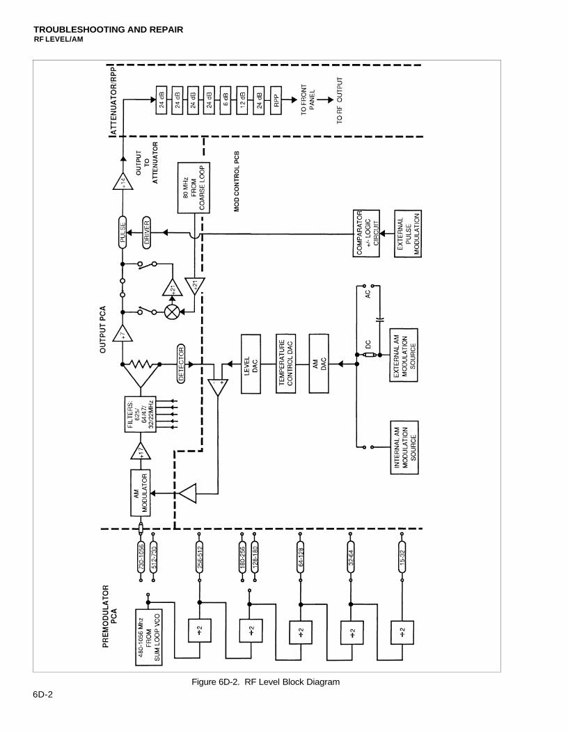
TROUBLESHOOTING AND REPAIRRF LEVEL/AM
6D-2Figure 6D-2. RF Level Block Diagram
TROUBLESHOOTING AND REPAIRRF LEVEL/AM
RF LEVEL CIRCUIT DESCRIPTION 6D-3.
The circuits on the A8 Output PCA, the A10 Premodulator PCA, and the A11Modulation Control PCA are interrelated and are described here as a unit. ThePremodulator PCA receives a 480 to 1056-MHz RF signal from the Sum Loop VCO,A9. The Premodulator PCA uses divide-by-two circuits and switches to develop a 15 to1056-MHz RF signal. This signal is applied to the Output PCA. The Output PCAcontains the level/AM modulator, generates a detected voltage for the leveling loop,develops the 0.01 to 14.999999-MHz HET BAND signal, contains the pulse modulatorcircuits, and provides the final amplification of the 0.01 to 1056 MHz output signal.The Modulation Control PCA distributes DC power and control signals to the OutputPCA, the Premodulator PCA, the FM PCA, and the Sum Loop PCA. It also controlsand distributes internal and external modulation signals for AM, FM, øM, and Pulsemodulation.
The Output Assembly provides a 0.01 to 1056-MHz RF signal to the A20Attenuator/RPP Assembly. The Attenuator/RPP provides 0 to 138-dB of attenu-ation in 6-dB steps and provides protection for the output circuits.
RF Path 6D-4.
The RF path begins with the 480 to 1056-MHz signal at J5 on the Premodulator PCA.This signal comes from the Sum Loop VCO PCA. A double-pole, double-throwswitch (CR1, CR2, CR3, CR4) sends this signal directly to amplifier U4 or through thedivide-by-two circuit, U2, and then to U4. The switch is controlled by the logic signalMIDH. Both paths use frequency-shaping networks to flatten the frequency response.The input frequency to U4 is then 240 to 1056 Mhz. The signal is further amplified byU5. The output of U5 is first low-pass filtered at 1100 MHz and then filtered again bythe switched filter that is controlled by logic signals HAOCTH and MIDH. This filterremoves harmonics with low-pass filters switched at 350 MHz, 512 MHz, and 730MHz. The particular filter in place depends on the logic state of HAOCTH and MIDHwhich control CR9-19.
The 240 to 1056-MHz signal goes to the double-pole, double-throw switch (CR22,CR23, CR31, CR32) which is controlled by the logic signal GT256H. This switchdirects the signal directly to the amplifier, Q6, or to the divider chain beginning withU11.
The U11 output is split. One output provides 128 to 256 MHz to a switched filter forreducing harmonics, and the other output provides an input signal to the third divider,U58. The 128 to 256-MHz output passes through a low-pass filter (selected by logicsignal GT180H) for frequencies below 180 MHz. Above that, frequency filtering isprovided by the 260-MHz LPF between U10 and CR31. When a frequency in this bandis selected, logic signal 1HAFH2 is high, which turns on CR71. The network betweenCR25,27, and CR71 provides level adjustment of the signal. U58 has two outputs. Oneoutput provides 64 to 128 MHz to an output filter consisting of T2 and the LPFfollowing it. The second output provides these same frequencies to the fourth divider,U8. U58 is activated by D1HAFL being high to provide DC bias and D2HAFH low toactivate the divider. U8 provides an output of 32 to 64 MHz. U8 and its output areselected by logic signals D3HAF and 3HAFH. The fifth divider, U9, generates 15 to 32MHz. U9 and its output are selected by logic signals D4HAFL and 4HAFH. Filteringfor harmonic suppression, when the frequency is in the 15 to 64-MHz range, is done onthe output board following the modulator. The appropriate band is selected by diodesCR71, CR28, CR29, or CR30 and is amplified by U10. When a frequency from 15 to256 MHz is selected, it passes to the amplifier Q6, through CR31. Q6 provides 6 dB ofgain and buffering for the 15 to 1056-MHz signal that is the input to the Output PCA.
6D-3
TROUBLESHOOTING AND REPAIRRF LEVEL/AM
The amplitude modulator on the Output PCA consists of PIN diodes CR27 throughCR33 and associated components, and the modulator receives the 15 to 1056-MHzsignal from the Premodulator PCA through W1. The modulator is a voltage-controlledvariable attenuator that provides AM and output level control. Modulator controlvoltage is determined by the leveling-loop circuitry. The leveling loop is described laterin this section.
Q5, U8, Q1, and associated components follow the modulator in the signal path andform a three-stage, 17-dB gain, 15 to 1056-MHz amplifier. This gain stage is followedby a 4-band switched filter to remove harmonics in the 15 to 27-MHz, 27 to 32-MHz,32 to 47-MHz, and 47 to 64-MHz frequency bands. For frequencies below 64 MHz,CR4 is on to direct these signals to the filter bank. The appropriate filter is selected byCR6-CR13, and the result is returned to the signal path by CR16. Signals above 64MHz proceed to this point via a high frequency, switched filter, (CR14, CR15, C38,C39, and circuit traces). This is a LPF for frequencies below 625 MHz to further reduceharmonics. The 64 to 1056-MHz signal is recombined with the 15 to 64-MHz signal atC180. This signal then drives a 3-dB power splitter that consists of resistors R63, R30,R31, and R32 and the associated transmission lines.
One power-splitter output drives the leveling loop detector diode CR20. The otheroutput goes to a 5.5-dB pad followed by a 7-dB amplifier, Q7 and associatedcomponents. The HET band switch follows the buffer amp and consists of PIN diodesCR18, CR21-24 and biasing components. In the 15 to 1056-MHz position, the signalpasses through diodes CR21 through CR24 to the pulse modulator, U5. A bufferamplifier follows the pulse modulator and consists of Q9 and associated components.This provides 8.5-dB of gain. This amplifier is then followed by the 6-dB finalamplifier, which is composed of Q16 and associated components. The final amplifierprovides at least +20 dBm output at low distortion.
For HET band operation (0.01 to 15 MHz), the signal from the power splitter is routedthrough CR18 to the HET band circuitry. The RF signal passes through a 95-MHzLPF, then an adjustable attenuator (R70 through R75), and then to the RF port of U3(a double-balanced mixer). The signal frequency at the mixer RF port varies from80.01 to 95 MHz. The 80-MHz local oscillator (LO) signal for the mixer comes fromthe A2 Coarse Loop PCA through J3 and is amplified by U1. This signal is thenamplified by class C amplifier Q10, which is followed by a band-pass filter and 3-dBpad to provide +18 dBm at the mixer LO port.
The mixer 0.01 to 15-MHz output signal is passed through a diplexing low-pass filter(C99 through C104, R76) that suppresses unwanted mixer spurious products whilemaintaining a 50-ohm load at the mixer IF port. The filtered IF signal is amplified by atwo-stage IF amplifier Q13, Q14, and associated components.
The IF amplifier gain is nominally 20 dB. The signal then is filtered to removeremaining LO and RF signals before being recombined at CR24 with the main signalpath. The +5V power supply for the LO amplifier is switched off by Q3 so that spurioussignals are not introduced when the instrument is operating in the 15 to 1056-MHzbands.
6D-4
TROUBLESHOOTING AND REPAIRRF LEVEL/AM
Leveling Loop 6D-5.
The leveling loop controls the 15 to 1056-MHz signal level at the detector diode (CR20)on the Output PCA; therefore the leveling loop also controls the signal level at thebuffer amplifier (Q7) on the Output PCA. The leveled RF signal is proportional to theleveling loop control voltage which appears at TP7 on the Modulation Control PCA.
The Schottky detector diode (CR20) generates a temperature-dependent DC voltage.This is a non-linear function of the applied RF voltage, thus temperature compensationand linearization are necessary. The detector diode signal is low-pass filtered by L34and C34, and is offset by the voltage across temperature-compensating diode CR19.Q1, Q2, and associated components on the Modulation Control PCA form a currentsource circuit that provides bias current for CR20 and CR19.
The offset detector diode voltage at U7 pin 3 on the Modulation Control PCA islinearized by amplifier U7 and its associated feedback components. PotentiometerR28 provides an adjustment for best detector linearity at low RF levels. Thus, thevoltage at U7 pin 6 (TP2) is proportional to the level of the RF signal incident on thedetector diode CR20 on the Output PCA.
This voltage is applied to pin 2 of the loop-integrator/summing amplifier, U41. Theleveling loop control voltage (plus any AM) is applied to pin 3 of U41. U41 drives theleveling/AM modulator through U14 and U15 and circuits that compensate formodulator non-linearity. R35, R36, CR5, and CR6 form an additional linearizingnetwork that acts on the control signal. Amplitude modulation is achieved bysumming an appropriately scaled modulation signal with the DC leveling loop controlvoltage.
The amplitude modulator on the Output PCA consists of PIN diodes CR27 throughCR33 and associated components. Attenuation through the modulator is a function ofbias current through these PIN diodes. This current is provided by the modulator-linearizer circuit on the Modulation Control PCA. U14 and associated componentsprovide modulator series diode current, while U15 and associated components provideshunt diode current.
Modulator attenuation is approximately proportional to the modulator controlvoltage on TP8. Proportionality is required to maintain constant leveling loopbandwidth as modulator attenuation varies. Minimum attenuation is obtained with amodulator control voltage of 10V, while maximum attenuation is obtained with 0V.
Comparator U10 and associated components form an unleveled indicator circuit. Thecomparator senses the modulator control voltage at TP8. This voltage is normally lessthan +11V, and the comparator output is high. If the modulator control voltageexceeds +11V, the modulator attenuation is at a minimum, and the leveling loopbecomes inoperative (unleveled). This condition could be due to a fault or someabnormal operation such as overmodulation. In this case, the comparator output(UNLVLL) goes low. The Controller PCA senses this low and causes the front panelSTATUS indicator to flash and displays an unleveled status code (241) if interrogated.
6D-5
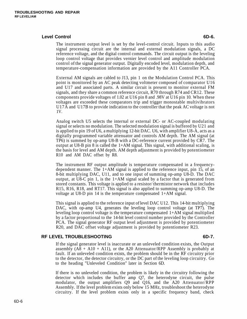
TROUBLESHOOTING AND REPAIRRF LEVEL/AM
Level Control 6D-6.
The instrument output level is set by the level-control circuit. Inputs to this audiosignal processing circuit are the internal and external modulation signals, a DCreference voltage, and the digital control commands. The circuit output is the levelingloop control voltage that provides vernier level control and amplitude modulationcontrol of the signal generator output. Digitally encoded level, modulation depth, andtemperature-compensation information are provided by the A11 Controller PCA.
External AM signals are cabled to J13, pin 1 on the Modulation Control PCA. Thispoint is monitored by an AC peak detecting voltmeter composed of comparator U16and U17 and associated parts. A similar circuit is present to monitor external FMsignals, and they share a common reference circuit, R70 through R74 and CR12. Thesecomponents provide voltages of 1.02 at U16 pin 8 and .98V at U16 pin 10. When thesevoltages are exceeded these comparators trip and trigger monostable multivibratorsU17 A and U17B to provide indication to the controller that the peak AC voltage is not1V.
Analog switch U5 selects the internal or external DC- or AC-coupled modulatingsignal or selects no modulation. The selected modulation signal is buffered by U21 andis applied to pin 19 of U6, a multiplying 12-bit DAC. U6, with amplifier U8-A, acts as adigitally programmed variable attenuator and controls AM depth. The AM signal (atTP6) is summed by op-amp U8-B with a DC-reference current provided by CR7. Theoutput at U8-B pin 8 is called the 1+AM signal. This signal, with additional scaling, isthe basis for level and AM depth. AM depth adjustment is provided by potentiometerR10 and AM DAC offset by R8.
The instrument RF output amplitude is temperature compensated in a frequency-dependent manner. The 1+AM signal is applied to the reference input, pin 15, of an8-bit multiplying DAC, U11, and to one input of summing op-amp U8-D. The DACoutput, at U8-C pin 1, is the 1+AM signal scaled by a factor that is generated fromstored constants. This voltage is applied to a resistor/ thermistor network that includesR15, R16, R18, and RT17. This signal is also applied to summing op-amp U8-D. Thevoltage at U8-D pin 14 is the temperature compensated 1+AM signal.
This signal is applied to the reference input of level DAC U12. This 14-bit multiplyingDAC, with op-amp U4, generates the leveling loop control voltage (at TP7). Theleveling loop control voltage is the temperature compensated 1+AM signal multipliedby a factor proportional to the 14-bit level control number provided by the ControllerPCA. The signal generator RF output level adjustment is provided by potentiometerR20, and DAC offset voltage adjustment is provided by potentiometer R23.
RF LEVEL TROUBLESHOOTING 6D-7.
If the signal generator level is inaccurate or an unleveled condition exists, the Outputassembly (A8 + A10 + A11), or the A20 Attenuator/RPP Assembly is probably atfault. If an unleveled condition exists, the problem should be in the RF circuitry priorto the detector, the detector circuitry, or the DC part of the leveling loop circuitry. Goto the heading "Unleveled Condition" later in Section 6D.
If there is no unleveled condition, the problem is likely in the circuitry following thedetector which includes the buffer amp Q7, the heterodyne circuit, the pulsemodulator, the output amplifiers Q9 and Q16, and the A20 Attenuator/RPPAssembly. If the level problem exists only below 15 MHz, troubleshoot the heterodynecircuitry. If the level problem exists only in a specific frequency band, check
6D-6
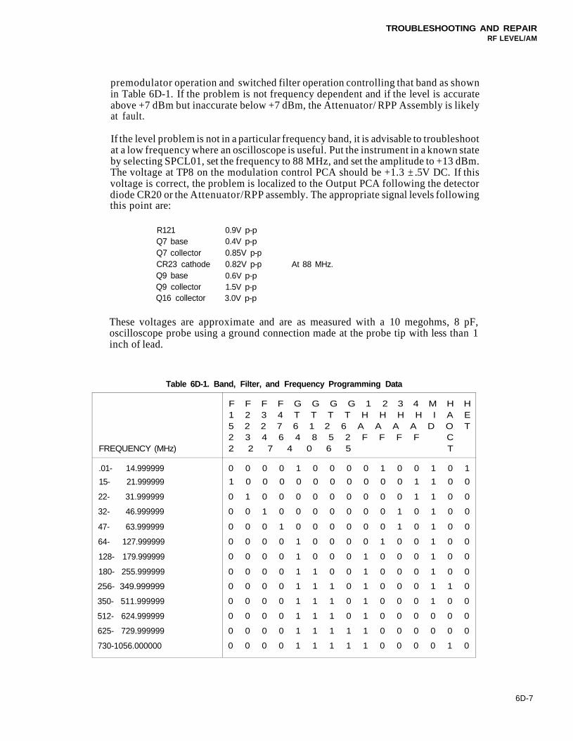
TROUBLESHOOTING AND REPAIRRF LEVEL/AM
premodulator operation and switched filter operation controlling that band as shownin Table 6D-1. If the problem is not frequency dependent and if the level is accurateabove +7 dBm but inaccurate below +7 dBm, the Attenuator/ RPP Assembly is likelyat fault.
If the level problem is not in a particular frequency band, it is advisable to troubleshootat a low frequency where an oscilloscope is useful. Put the instrument in a known stateby selecting SPCL01, set the frequency to 88 MHz, and set the amplitude to +13 dBm.The voltage at TP8 on the modulation control PCA should be +1.3 ± .5V DC. If thisvoltage is correct, the problem is localized to the Output PCA following the detectordiode CR20 or the Attenuator/RPP assembly. The appropriate signal levels followingthis point are:
R121Q7 baseQ7 collectorCR23 cathodeQ9 baseQ9 collectorQ16 collector
0.9V p-p0.4V p-p0.85V p-p0.82V p-p0.6V p-p1.5V p-p3.0V p-p
At 88 MHz.
These voltages are approximate and are as measured with a 10 megohms, 8 pF,oscilloscope probe using a ground connection made at the probe tip with less than 1inch of lead.
Table 6D-1. Band, Filter, and Frequency Programming Data
FREQUENCY (MHz)
.01- 14.999999
15- 21.999999
22- 31.999999
32- 46.999999
47- 63.999999
64- 127.999999
128- 179.999999
180- 255.999999
256- 349.999999
350- 511.999999
512- 624.999999
625- 729.999999
730-1056.000000
F F F F G G G G 1 2 3 4 M H H1 2 3 4 T T T T H H H H I A E5 2 2 7 6 1 2 6 A A A A D O T2 3 4 6 4 8 5 2 F F F F C2 2 7 4 0 6 5 T
0 0 0 0 1 0 0 0 0 1 0 0 1 0 1
1 0 0 0 0 0 0 0 0 0 0 1 1 0 0
0 1 0 0 0 0 0 0 0 0 0 1 1 0 0
0 0 1 0 0 0 0 0 0 0 1 0 1 0 0
0 0 0 1 0 0 0 0 0 0 1 0 1 0 0
0 0 0 0 1 0 0 0 0 1 0 0 1 0 0
0 0 0 0 1 0 0 0 1 0 0 0 1 0 0
0 0 0 0 1 1 0 0 1 0 0 0 1 0 0
0 0 0 0 1 1 1 0 1 0 0 0 1 1 0
0 0 0 0 1 1 1 0 1 0 0 0 1 0 0
0 0 0 0 1 1 1 0 1 0 0 0 0 0 0
0 0 0 0 1 1 1 1 1 0 0 0 0 0 0
0 0 0 0 1 1 1 1 1 0 0 0 0 1 0
6D-7
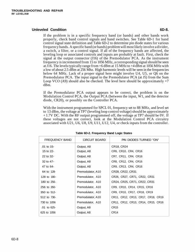
TROUBLESHOOTING AND REPAIRRF LEVEL/AM
Unleveled Condition 6D-8.
If the problem is in a specific frequency band (or bands) and other bands workproperly, check band control signals and band switches. See Table 6D-1 for bandcontrol signal state definition and Table 6D-2 to determine pin diode states for variousfrequency bands. A specific band (or bands) problem will most likely involve a divider,a switch, a filter, or a control signal. If all of the frequency bands are affected, theleveling loop or associated controls and inputs are probably at fault. First, check thesignal at the output connector (J16) of the Premodulator PCA. As the instrumentfrequency is incremented from 15 to 1056 MHz, a corresponding signal should be seenat J16. The levels typically range from +6 dBm at 15 MHz to +4 dBm at 1056 MHz witha low of about 2.5 dBm at 256 Mhz. High harmonic levels will be seen in the frequenciesbelow 64 MHz. Lack of a proper signal here might involve U4, U5, or Q6 on thePremodulator PCA. The input signal to the Premodulator PCA (at J5) from the SumLoop VCO (A9) should also be checked. The level here should be approximately +7dBm.
If the Premodulator PCA output appears to be correct, the problem is on theModulation Control PCA, the Output PCA (between the input, W1, and the detectordiode, CR20), or possibly on the Controller PCA.
With the instrument programmed for SPCL 01, frequency set to 88 MHz, and level setto 13 dBm, the voltage at TP7 (leveling loop control voltage) should be approximately+ 1.7V DC. With the RF output programmed off, the voltage at TP7 should be 0V. Ifthese voltages are not correct, look at the Modulation Control PCA circuitryassociated with U21, U6, U8, U9, U11, U12, U4, or check inputs from the controller.
Table 6D-2. Frequency Band Logic States
6D-8
FREQUENCY BAND
.01 to 15-
15 to 22-
22 to 32-
32 to 47-
47 to 64-
64 to 128-
128 to 180-
180 to 256-
256 to 350-
350 to 512-
512 to 730-
730 to 1056
.01 to 625-
625 to 1056
CIRCUIT BOARD
Output, A8
Output, A8
Output, A8
Output, A8
Output, A8
Premodulator, A10
Premodulator, A10
Premodulator, A10
Premodulator, A10
Premodulator, A10
Premodulator, A10
Premodulator, A10
Output, A8
Output, A8
PIN DIODES TURNED "ON"
CR18, CR24
CR6, CR10, CR4, CR16
CR7, CR11, CR4, CR16
CR8, CR12, CR4, CR16
CR9, CR13, CR4, CR16
CR28, CR22, CR31
CR26, CR27, CR71, CR22, CR31
CR24, CR25, CR71, CR22, CR31
CR9, CR10, CR14, CR15, CR16
CR9, CR10, CR17, CR18, CR19
CR11, CR12, CR13, CR17, CR18, CR19
CR11, CR12, CR13, CR14, CR15, CR16
CR15
CR14
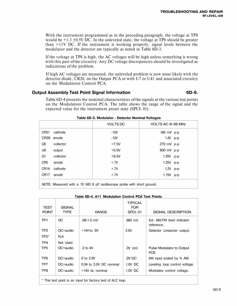
TROUBLESHOOTING AND REPAIRRF LEVEL/AM
With the instrument programmed as in the preceding paragraph, the voltage at TP8would be +1.3 ±0.5V DC. In the unleveled state, the voltage at TP8 should be greaterthan +11V DC. If the instrument is working properly, signal levels between themodulator and the detector are typically as noted in Table 6D-3.
If the voltage at TP8 is high, the AC voltages will be high unless something is wrongwith this part of the circuitry. Any DC voltage discrepancies should be investigated asindications of the problem.
If high AC voltages are measured, the unleveled problem is now most likely with thedetector diode, CR20, on the Output PCA or with U7 or U41 and associated circuitryon the Modulation Control PCA.
Output Assembly Test Point Signal Information 6D-9.
Table 6D-4 presents the nominal characteristics of the signals at the various test pointson the Modulation Control PCA. The table shows the range of the signal and theexpected value for the instrument preset state (SPCL 01).
Table 6D-3. Modulator - Detector Nominal Voltages
Table 6D-4. A11 Modulation Control PCA Test Points
6D-9
CR31 cathode
CR28 anode
Q5 collector
U8 output
Q1 collector
CR5 anode
CR14 cathode
CR17 anode
VOLTS DC
-15V
-12V
+7.5V
+5.5V
+9.5V
+.7V
+.7V
+.7V
VOLTS AC @ 88 MHz
180 mV p-p
1.2V p-p
270 mV p-p
600 mV p-p
1.25V p-p
1.25V p-p
1.2V p-p
1.15V p-p
NOTE: Measured with a 10 MΩ 8 pF oscilloscope probe with short ground.
TESTPOINT
TP1
TP2
TP3*
TP4
TP5
TP6
TP7
TP8
SIGNALTYPE
DC
DC+audio
N/A
Not Used
DC+audio
DC+audio
DC+audio
DC+audio
RANGE
.98 ± 5 mV
+14V to 0V
.2 to 4V
0 to 2.8V
0.04 to 3.0V DC nominal
+14V dc nominal
TYPICALFOR
SPCL 01
.980 mV
2.6V
.3V (on)
.0V DC
1.0V DC
1.0V DC
SIGNAL DESCRIPTION
Ext. AM/FM level indicator
reference.
Detector Linearizer output.
Pulse Modulator to OutputPCB.
AM input scaled by % AM.
Leveling loop control voltage.
Modulator control voltage.
* This test point is an input for factory test of ALC loop.
TROUBLESHOOTING AND REPAIRRF LEVEL/AM
RF LEVEL ADJUSTMENTS 6D-10.
The Output Section adjustments listed below are covered in the following paragraphs:
• Modulation Control PCA, A11
R23, Level DAC Offset AdjustmentR8, AM DAC Offset AdjustmentR28, Detector Offset/Linearity AdjustmentR10, AM Depth AdjustmentR20, RF Level AdjustmentR71, External Modulation Level Indicator AdjustmentR99, Sum Loop Steer Gain Adjustment
• Premodulator PCA, A10
R51, C7, AM Bandwidth Adjustment
• Output PCA, A8
R96, Q16 Bias AdjustmentR1, Q9 Bias AdjustmentR72, Het Mixer Level AdjustmentR10, Het Gain AdjustmentC201, Gain Flatness Adjustment
R82, R101, and R102 are related to FM performance and are discussed under theheading "Alignment of FM PCA (A14)" in Section 6E.
Any adjustment can be made independently unless it is noted that it interacts withanother adjustment. Interdependent adjustments must be done in the sequencepresented. If more than one adjustment is necessary, do them in the sequencepresented.
Mod Control PCA Level DAC Offset Adjustment, R23 6D-11.
TEST EQUIPMENT:
• DVM
REMARKS:
The level DAC offset adjustment is normally required only when U4 or any associatedcomponents are replaced.
CAUTION
This adjustment directly affects the output level and should not be madeindiscriminately.
PROCEDURE:
The level DAC offset, R23, is adjusted for 0 ±0.5 mV at TP7 with the RF OUTPUToff.
6D-10
TROUBLESHOOTING AND REPAIRRF LEVEL/AM
1. Access R23 by removing the bottom instrument cover and removing the bottommodule cover.
2. Program the UUT to SPCL 01, and program the RF OUTPUT to OFF.
3. Connect the DVM to measure the voltage between TP7 and ground on the moduleplate.
4. Adjust R23 for an indication of 0 mV ±0.5 mV.
5. Program the UUT RF OUTPUT to ON.
6. Reinstall the module plate cover and instrument cover when the adjustments arecomplete.
Mod Control PCA AM DAC Offset Adjustment, R8 6D-12.
TEST EQUIPMENT:
• DVM
REMARKS:
The AM DAC offset adjustment is normally required only when U8 or any associatedcomponents are replaced.
CAUTION
This adjustment directly affects the output level and should not be madeindiscriminately.
PROCEDURE:
The AM DAC offset, R8, is adjusted for 0 ±0.5 mV at TP6 with AM off.
1. Access R8 by removing the bottom instrument cover and the bottom module platecover.
2. Program the UUT to SPCL 01.
3. Connect the DVM to measure the voltage between TP6 and ground on the moduleplate.
4. Adjust R8 for an indication of 0 mV ±0.5 mV.
5. Reinstall the nodule plate cover and the instrument cover when the adjustmentsare complete.
6D-11
TROUBLESHOOTING AND REPAIRRF LEVEL/AM
Mod Control PCA Detector Offset Adjustment, R28 6D-13.
The detector offset adjustment sets the detector offset voltage. The adjustment alsoaffects AM Depth Adjustment, R10. Repeat Section 6D-14 after this adjustment.
TEST EQUIPMENT:
• Power meter• Power sensor (High-Level)
REMARKS:
The UUT must be operated at room temperature for at least one hour with the moduleplate cover in place before continuing with this adjustment procedure.
This adjustment is normally required only when components in the detector ordetector linearizer circuits have been replaced. If the detector offset is adjusted,perform the AM depth adjustment.
CAUTION
The detector offset adjustment directly affects the output level and shouldnot be made indiscriminately.
PROCEDURE:
The detector offset adjustment, R28, is adjusted to provide a 24-dB change in outputpower for a 24-dB change in the level DAC. This is done while operating in fixed range.
1. Access R28 by removing the instrument bottom cover.
2. Program the UUT to SPCL 01, 350 MHz and +12 dBm.
3. Program the UUT to SPCL 51. This Special Function enables amplitude fixedrange.
4. Remove the detector offset adjustment access screw from the bottom module platecover.
5. Zero the power meter.
6. Connect the power sensor to the UUT RF OUTPUT connector.
7. Note the power meter reading.
8. Program the UUT for -12 dBm using the EDIT knob. Be certain to use the EDITknob to change the amplitude for this step or the special function will beautomatically cleared.
9. Adjust the detector offset adjustment, R28, for a power meter reading 23 dB ±0.1dB below the reading obtained in step 7. Program the UUT to +12 dBm.
10. Repeat steps 7 through 9 until the difference between the power measurements is23 ±0.1 dB. This adjustment should require three or fewer iterations.
6D-12
TROUBLESHOOTING AND REPAIRRF LEVEL/AM
11. Use the EDIT knob to program the UUT to +17 dBm. Note the power meterreading.
12. Use the EDIT knob to program the UUT for +2 dBm. Verify that the power meterreading is 15 dB ±0.2 dB below the previous reading.
13. Program the UUT for SPCL 50. This disables amplitude fixed range.
14. Disconnect the power sensor from the UUT, and replace the detector offsetadjustment access screw.
Mod Control PCA AM Depth Adjustment, R10 6D-14.
TEST EQUIPMENT:
• DVM• Modulation Analyzer• Low-Frequency Synthesized Signal Generator (LFSSG)
REMARKS:
The UUT must be operated at room temperature for at least one hour with the moduleplate covers in place before continuing with this adjustment procedure.
CAUTION
The AM depth adjustment directly affects the output level and should not bemade indiscriminately.
The AM depth adjustment is normally required only when components in the AMsignal processing circuits have been replaced. If this adjustment is made, it is thennecessary to repeat 6D-13 (Detector Offset Adjustment, R28) and perform the RFLevel Adjustment, R20.
PROCEDURE:
Adjust the AM depth adjustment, R10, for 90% AM depth as measured with theModulation Analyzer when the UUT is programmed to 90% AM.
1. Remove the AM depth adjustment access screw from the bottom module platecover.
2. Connect the output of the LFSSG to the UUT MOD IN connector and to theDVM using a BNC Tee.
3. Program the UUT to SPCL 01, 350 MHz, +4 dBm, and EXT AM AT 90% AMDEPTH.
4. Program the LFSSG for 1 KHz and a voltage of 0.7071 RMS as measured by theDVM.
5. Connect the UUT RF OUTPUT connector to the modulation analyzer input.
6. Program the modulation analyzer to measure AM + Peak, in a 0.05- to 15-kHzbandwidth.
6D-13
TROUBLESHOOTING AND REPAIRRF LEVEL/AM
7. Alternately measure +PEAK and -PEAK, and adjust the AM depth adjustment,R10, until the readings are symmetrical about 90%.
8. Reinstall the AM depth adjustment access screw.
Mod Control PCA RF Level Adjustment, R20 6D-15.
TEST EQUIPMENT:
• Power meter• Power sensor (High-Level)
REMARKS:
The UUT must be operated at room temperature for at least one hour with the moduleplate covers in place before continuing with this adjustment procedure.
This adjustment is required if any of the following events occur:
• The Output PCA, the Modulation Control PCA, or the Attenuator/RPPAssembly has been replaced.
• The AM depth adjustment is made.
• The level DAC or any associated components are replaced.
• The RF level adjustment has been inadvertently changed.
CAUTION
The RF level adjustment directly affects the output level and should not bemade indiscriminately.
PROCEDURE:
With the UUT programmed to +9 dBm, adjust the RF level adjustment, R20, for +9dBm output as measured with the Power Meter.
1. Program the UUT to SPCL 01, 350 MHz, and +9 dBm.
2. Zero the power meter.
3. Remove the RF level adjustment access screw from the bottom module platecover.
4. Connect the power sensor to the UUT RF connector.
5. Adjust RF level adjustment, R20, for a reading of exactly +9 dBm on the PowerMeter.
6. Reinstall the RF level adjustment access screw.
6D-14
TROUBLESHOOTING AND REPAIRRF LEVEL/AM
Mod Control PCA External Modulation Level Indicator Adjustment, R71 6D-16.
TEST EQUIPMENT:
• DVM
REMARKS:
This adjustment is normally made if CR12 or R70-R74 are replaced.
PROCEDURE:
The potentiometer is adjusted to provide 0.98V DC at TP1. This adjusts both AM andFM indicators, as the remaining levels are set by fixed resistors.
1. Remove the bottom instrument cover and remove the access screws for TP1 andR71.
2. Connect the DVM to TP1 and ground.
3. Set the UUT to SPCL 01 and observe the DVM.
4. Adjust R71 for 0.980 volts.
5. Reinstall the access screws and bottom cover.
Mod Control PCA Sum Steer Gain Adjustment, R99 6D-17.
TEST EQUIPMENT:
• DVM
REMARKS:
The Sum Steer Gain Adjustment is normally required only when U32, U36, or anyassociated components are replaced.
PROCEDURE:
The sum steer voltage is adjusted to 10.24V with the Sum Loop VCO steering DAC setto full scale.
1. Program the UUT to SPCL 01.
2. Program the UUT to SPCL 942. This Special Function programs all DACs to fullscale.
3. Connect the DVM to measure the voltage between J2 pin 14 and module ground.
4. Adjust R99 for 10.24V ± .01V.
5. Program the UUT for SPCL 00. This clears all Special Functions.
6D-15
TROUBLESHOOTING AND REPAIRRF LEVEL/AM
Output PCA Het Mixer Level Adjustment, R72 6D-18.
TEST EQUIPMENT:
• Power meter• Power sensor (High-Level)• Spectrum analyzer
REMARKS:
The UUT must be operated at room temperature for at least one hour with the modulecovers in place before continuing with this adjustment procedure.
This adjustment is normally required only when mixer U4 or het band LO circuitry isreplaced. When adjusted, an interaction with R10 exists, therefore R10 adjustment isincluded in this procedure.
CAUTION
This adjustment directly affects the output level and should not be madeindiscriminately.
PROCEDURE:
With the UUT programmed to +16 dBm and 14.9 MHz, the worst in band spur isadjusted to be well within specification. A lower level of this spur degrades thebroadband noise in the het band. The het level is then appropriately readjusted.
1. Remove bottom cover and appropriate access screws on bottom module plate forR10 and R72.
2. Program UUT to SPCL 01, 15 MHz, and +16 dBm. Connect the power meter tothe output of the UUT. Edit the level to +16 dBm. Set the power meter to dB(ref).
3. Edit the frequency to 14.9 MHz and adjust R10 for 0 dB(REL)
4. Connect the spectrum analyzer to the UUT and observe the spur at 5.5 MHz. Thisspur should be observed with high spectrum analyzer attenuation (typically 30 dB)to avoid internal analyzer spurs. The resolution bandwidth and span should benarrow (typically a span of 1 kHz and resolution bandwidth of 10 Hz) to allow thespur to be seen clearly.
5. Adjust the spur to a level of -89 dBm ±2 dB with R72. This has changed theadjustment in step 3 above so steps 3 through 5 must be sequenced again until levelis 0 dB(REL)±.l dB.
6. Reinstall the access screws.
6D-16
TROUBLESHOOTING AND REPAIRRF LEVEL/AM
Output PCA Het Level Adjustment, R10 6D-19.
TEST EQUIPMENT:
• Power meter• Power sensor (High-Level)
REMARKS:
The UUT must be operated at room temperature for at least one hour with the moduleplate covers in place before continuing with this adjustment procedure.
This adjustment is normally required only when components in the het band circuitshave been replaced. It is also necessary to make this adjustment if R72 is adjusted.
CAUTION
This adjustment directly affects the output level and should not be madeindiscriminately.
PROCEDURE:
With the UUT programmed to +9 dBm, adjust the het level adjustment, R10, for equaloutput power at 14.9 and 15 MHz.
1. Program the UUT to SPCL 01, 15 MHz, and +9 dBm.
2. Zero the power meter.
3. Remove the het level adjustment access screw from the bottom module plate cover.
4. Connect the Power Sensor to the UUT RF OUTPUT connector. Note the powermeter reading.
5. Program the UUT to 14.9 MHz.
6. Adjust the het level adjustment, R10, for a reading equal to that previously noted.
7. Reinstall the het level adjustment access screw.
Premodulator PCA Bandwidth Adjustment, R51 and C7 6D-20.
The following procedure covers the adjustment of R51 and C7 on the PremodulatorPCA. This adjustment optimizes the AM bandwidth in the 256 to 1056-MHz band.
TEST EQUIPMENT:
• Power meter• Tuning tool, .025 in. sq., Johanson #4192
REMARKS:
This adjustment is normally made only if changes are made to the Premodulator PCA.
6D-17
TROUBLESHOOTING AND REPAIRRF LEVEL/AM
PROCEDURE:
R51 is adjusted so that the Premodulator output is 3.5 dBm at 800 MHz. Assumingthat the shape of the control voltage versus frequency curve is typical, this minimizesthe overall variation and thereby minimizes loop gain variation and consequentlyminimizes bandwidth variation. C7 is adjusted adjusted to give the optimum level outof the Premodulator PCA at 1056 MHz.
1. Remove bottom instrument cover and bottom module plate cover.
2. Program the UUT to SPCL 01, 800 MHz, and +7 dBm. Measure the output powerof the Premodulator PCA by disconnecting the cable from J16 on the Premodu-lator PCA and connecting the power meter. Adjust R51 for 3.5 dBm.
3. Edit the frequency to 1056 MHz and observe the power again. Adjust C7 to obtain4.5 dBm +.5 dB.
4. Repeat steps 2 through 4.
5. Remove the power meter and move the cable from the output board to J16 on thePremodulator PCA.
6. Reinstall the bottom module cover and the bottom cover.
Output PCA Q16 Bias Adjustment, R96 6D-21.
The following procedure covers the adjustment of R96 on the Output PCA.
TEST EQUIPMENT:
• DVM
REMARKS:
This adjustment is required only if Q16 or any associated parts are replaced. Thisadjustment sets the bias current in the output transistor for designed operatingconditions.
PROCEDURE:
R96 is adjusted for 1.355V DC between TP1 and TP2.
1. Remove the bottom cover of the instrument, the bottom module cover, and thepulse cover. This allows access to both the test points and R96.
2. Place the positive (+) lead of the DVM on TP2 and the negative (-) lead on TP1. Setthe DVM to VDC and the 2 volt range.
3. Turn the signal generator on and let it operate for 15 minutes. Program the UUTwith SPCL 01.
4. Adjust R96 until the DVM reads 1.355V DC.
5. Reinstall the pulse cover, the module cover, and the instrument bottom cover.
6D-18
TROUBLESHOOTING AND REPAIRRF LEVEL/AM
Output PCA Q9 Bias Adjustment, R1 6D-22.
The following procedure covers the bias adjustment of Q9 on the Output PCA.
TEST EQUIPMENT:
• Spectrum analyzer
REMARKS:
This adjustment is normally made only when Q9 or associated circuitry is replaced.
PROCEDURE:
Rl adjusts the collector current of Q9 to minimize harmonic distortion.
1. Remove the bottom instrument cover, bottom module plate cover, and the pulsecover.
2. Connect UUT RF Output to the spectrum analyzer. Set the spectrum analyzersweep to cover the frequency range of 1 to 1300 MHz and set the analyzer referencelevel to +13 dBm.
3. Set UUT to SPCL 01 and amplitude to +13 dBm.
4. Edit the frequency to display signal and harmonics on the spectrum analyzer.Adjust R1 to minimize the worst harmonic seen. This is typically the secondharmonic with the UUT frequency at about 300 MHz. The harmonic must be lessthan 30 dBc for proper operation.
5. Reinstall the pulse cover, the module plate cover, and the instrument cover.
Output PCA Gain Flatness Adjustment, C201 6D-23.
This procedure describes the adjustment of C201 for the purpose of optimizing gainflatness. This adjustment should not be required unless CR20 (detector diode) or partsin the RF path following C180 are replaced. This adjustment should be followed byoutput compensation. See Appendix H.
TEST EQUIPMENT:
• Power meter• Tuning tool, .025 in. square, Johanson #4192
PROCEDURE:
1. Zero the power meter
2. Program the UUT to SPCL 01, 350 MHz, and +7 dBm. Connect the power meterto the UUT RF output.
3. Set the power meter to dB REF.
4. Edit the UUT frequency from 15 to 1056 MHz and note the variation in level.Adjust C201 to minimize the level variation. C201 will have the greatest effect athigh frequencies. Level should be flat with a maximum allowed variation of 3dB.
6D-19
TROUBLESHOOTING AND REPAIRRF LEVEL/AM
FM Gain Adjustment, R82, on Mod Control PCA 6D-24.
See "Alignment of FM PCA" in Section 6E.
FM steer Gain, R101 on Mod Control PCA 6D-25.
See "Alignment of FM PCA" in Section 6E.
FM INV Balance, R102 on Mod Control PCA 6D-26.
See "Alignment of FM PCA" in Section 6E.
ATTENUATOR/REVERSE POWER PROTECTION (RPP) 6D-27.
The A20 Attenuator/RPP Assembly consists of the A21 Attenuator/RPP PCA, theA7 Relay Driver PCA, and a metal housing. The Attenuator/ RPP PCA is mountedinside the housing and the Relay Driver is attached on top of the housing. Thisassembly is mounted to the Output Module, opposite the Output PCA. The outputsignal of the Output PCA (at P1) is the input to the Attenuator/RPP PCA (at J1).
The Attenuator section of the Attenuator/ RPP PCA provides an attenuation range of0 to 138 dB in 6-dB steps. This is accomplished by seven, independently cascaded,50-ohm attenuation sections (K1 through K7). There are one 6-dB, one 12-dB, and five24-dB sections. Each section consists of a DPDT relay and a pi attenuator pad. Onerelay position (when DC power is applied to the relay), provides a low-loss throughpath for the RF signal. The other position (no DC power applied to the relay), insertsthe attenuator into the RF signal path. Control of the sections is from the ControllerPCA through the Relay Driver PCA. Attenuation correction data for each attenuatoris stored in the compensation memory on the Controller PCA. Necessary correction isapplied via the leveling loop control voltage.
The RPP section of the Attenuator/RPP PCA protects the attenuator and the outputamplifier from excess applied DC voltage or RF power. C6 and C7 provide a DCvoltage block. K8, when in the protect position (no DC power applied to the relay),protects against long duration excess RF power. The detector diode (CR1) sensesexcess RF power and trips the latching comparator circuit (U1-A) on the Relay DriverPCA. This change of state of U1-A passes through U1-D, Q8, and Q9 to remove theDC power from K8. This puts K8 into the protect state. Diodes CR2 through CR9 onthe Attenuator/RPP PCA form an RF limiter circuit. This provides protection againstshort duration excess power events or until K8 can change state. This may take up to 4ms. When the latching comparator (U1-A), on the Relay Driver PCA, changes to thetripped state, the positive voltage on U1-A pin 1 is applied to the inverting input ofU1-C causing the output of U1-C to go low (approximately 0V DC). This signal(RPTRPL) informs the Controller that the RPP has been tripped which causes theinstrument to go into the RF OFF state and flashes the STATUS light. Diodes CR8and 9 provide bias voltage for the limiter diodes to set the limiting threshold. Theexcess power detection threshold (for CR1 on the Attenuator/RPP PCA) is set by theresistor network at the input of U1-A.
6D-20
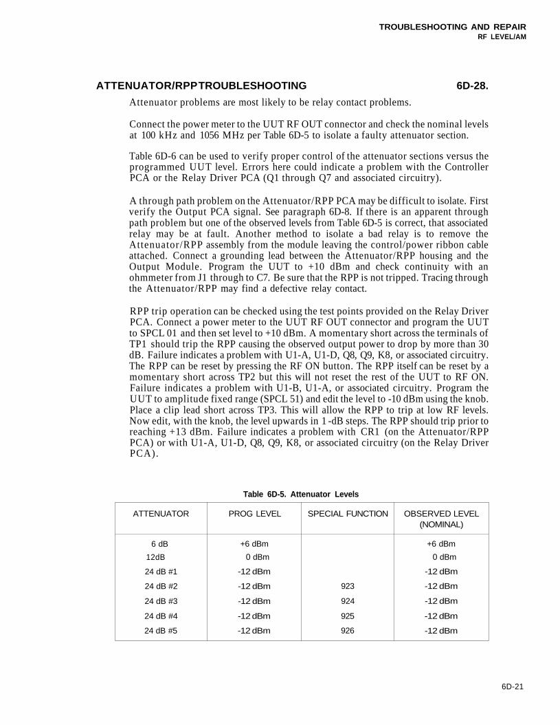
TROUBLESHOOTING AND REPAIRRF LEVEL/AM
ATTENUATOR/RPP TROUBLESHOOTING 6D-28.
Attenuator problems are most likely to be relay contact problems.
Connect the power meter to the UUT RF OUT connector and check the nominal levelsat 100 kHz and 1056 MHz per Table 6D-5 to isolate a faulty attenuator section.
Table 6D-6 can be used to verify proper control of the attenuator sections versus theprogrammed UUT level. Errors here could indicate a problem with the ControllerPCA or the Relay Driver PCA (Q1 through Q7 and associated circuitry).
A through path problem on the Attenuator/RPP PCA may be difficult to isolate. Firstverify the Output PCA signal. See paragraph 6D-8. If there is an apparent throughpath problem but one of the observed levels from Table 6D-5 is correct, that associatedrelay may be at fault. Another method to isolate a bad relay is to remove theAttenuator/RPP assembly from the module leaving the control/power ribbon cableattached. Connect a grounding lead between the Attenuator/RPP housing and theOutput Module. Program the UUT to +10 dBm and check continuity with anohmmeter from J1 through to C7. Be sure that the RPP is not tripped. Tracing throughthe Attenuator/RPP may find a defective relay contact.
RPP trip operation can be checked using the test points provided on the Relay DriverPCA. Connect a power meter to the UUT RF OUT connector and program the UUTto SPCL 01 and then set level to +10 dBm. A momentary short across the terminals ofTP1 should trip the RPP causing the observed output power to drop by more than 30dB. Failure indicates a problem with U1-A, U1-D, Q8, Q9, K8, or associated circuitry.The RPP can be reset by pressing the RF ON button. The RPP itself can be reset by amomentary short across TP2 but this will not reset the rest of the UUT to RF ON.Failure indicates a problem with U1-B, U1-A, or associated circuitry. Program theUUT to amplitude fixed range (SPCL 51) and edit the level to -10 dBm using the knob.Place a clip lead short across TP3. This will allow the RPP to trip at low RF levels.Now edit, with the knob, the level upwards in 1 -dB steps. The RPP should trip prior toreaching +13 dBm. Failure indicates a problem with CR1 (on the Attenuator/RPPPCA) or with U1-A, U1-D, Q8, Q9, K8, or associated circuitry (on the Relay DriverPCA).
Table 6D-5. Attenuator Levels
6D-21
ATTENUATOR
6 dB
12dB
24 dB #1
24 dB #2
24 dB #3
24 dB #4
24 dB #5
PROG LEVEL
+6 dBm
0 dBm
-12 dBm
-12 dBm
-12 dBm
-12 dBm
-12 dBm
SPECIAL FUNCTION
923
924
925
926
OBSERVED LEVEL(NOMINAL)
+6 dBm
0 dBm
-12 dBm
-12 dBm
-12 dBm
-12 dBm
-12 dBm
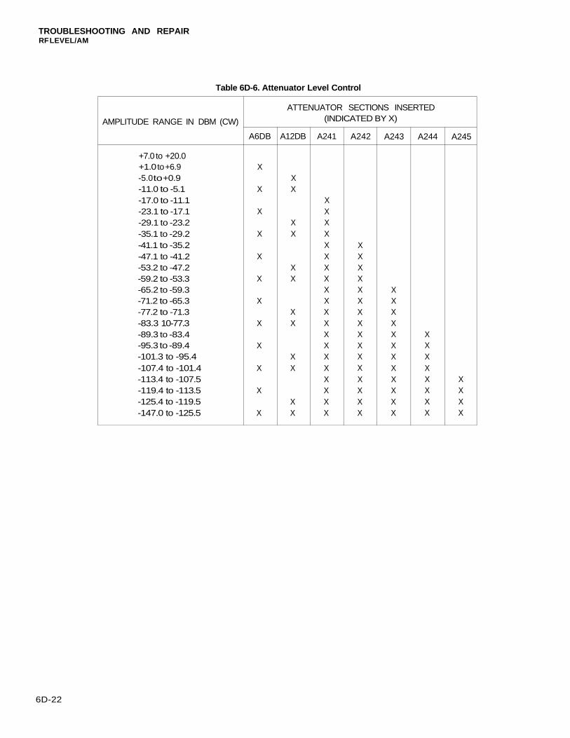
TROUBLESHOOTING AND REPAIRRF LEVEL/AM
Table 6D-6. Attenuator Level Control
6D-22
AMPLITUDE RANGE IN DBM (CW)
+7.0 to +20.0+1.0 to +6.9-5.0 to +0.9-11.0 to -5.1-17.0 to -11.1-23.1 to -17.1-29.1 to -23.2-35.1 to -29.2-41.1 to -35.2-47.1 to -41.2-53.2 to -47.2-59.2 to -53.3-65.2 to -59.3-71.2 to -65.3-77.2 to -71.3-83.3 10-77.3-89.3 to -83.4-95.3 to -89.4-101.3 to -95.4-107.4 to -101.4-113.4 to -107.5-119.4 to -113.5-125.4 to -119.5-147.0 to -125.5
ATTENUATOR SECTIONS INSERTED(INDICATED BY X)
A6DB
X
X
X
X
X
X
X
X
X
X
X
X
A12DB
XX
XX
XX
XX
XX
XX
A241
XXXXXXXXXXXXXXXXXXXX
A242
XXXXXXXXXXXXXXXX
A243
XXXXXXXXXXXX
A244
XXXXXXXX
A245
XXXX
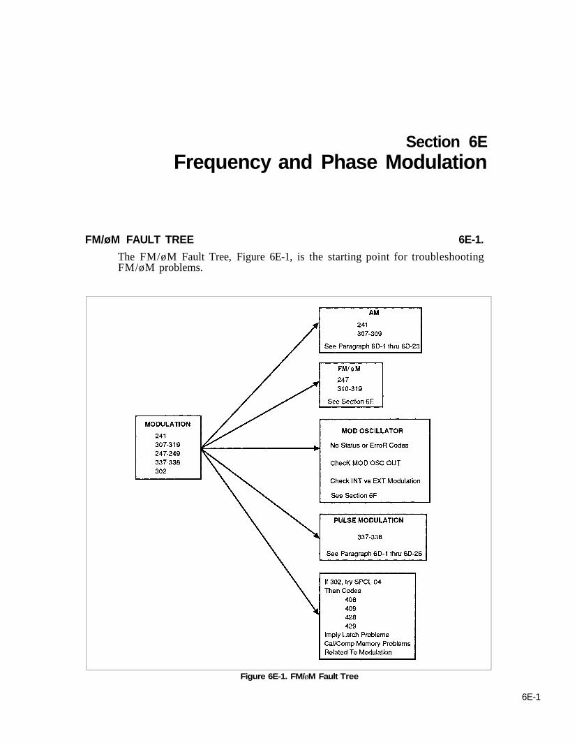
Section 6EFrequency and Phase Modulation
FM/øM FAULT TREE 6E-1.
The FM/øM Fault Tree, Figure 6E-1, is the starting point for troubleshootingFM/øM problems.
6E-1
Figure 6E-1. FM/øM Fault Tree
TROUBLESHOOTING AND REPAIRFREQUENCY AND PHASE MODULATION
FM/ØM BLOCK DIAGRAM 6E-2.
Refer to the FM/øM Block Diagram (Figure 6E-2) to identify the major functionalsections and in follow the signal paths of the FM section.
FM/ØM CIRCUIT DESCRIPTION 6E-3.
The FM PCA, (A14), has a phase-locked loop that consists of the following:
• Voltage-controlled 80-MHz oscillator with a modulation port, a control port, anda presteering section.
• Programmable dividers for reference and variable frequencies.
• Selectable phase detectors, normal and wide range, loop amplifier and filtercircuitry, and logic circuitry.
• Modulation section with both high modulation rate path and low modulation ratepath.
Incorporated in the different sections are logic and controls for achieving frequencymodulation, normal and low rate, and phase modulation, normal and high rate. Also,the function of DC frequency modulation is included. The FM modulation deviation is4 MHZ maximum, which is covered in six ranges. Equivalent phase modulation rangesexist for 400 Radians maximum (40 Radians maximum in high-rate phase modulation).To attain such a wide deviation the oscillator has a high deviation mode in the top twodeviation ranges. A linearizer is active in the top three ranges to reduce distortion. Toachieve the wide range deviation at low rates, a wide band phase detector is used for thetop deviation ranges, and the phase detector reference frequency is appropriatelyselected.
Oscillator Section 6E-4.
The voltage controlled oscillator section is composed of Q1, Q2, L1, CR1-CR8 andassociated components. The adjustable coil L1, adjustable capacitor C9, varactors(voltage variable capacitors) CR1-CR8, and associated capacitors form the resonantcircuit. Capacitors C2 and C4 couple the resonant circuit to the input of the activecircuit and C10, C11, and C13 couple to the output of the active circuit. Parts C9,CR15, and L4 are used to switch between the high deviation mode and normal mode.The circuit of Q5 and Q8 drive the PIN diode CR15 between either conduction or highimpedance. Low impedance at conduction adds C9 in the resonant circuit for a normalmode high "Q" oscillator circuit. High impedance removes C9 from the oscillator forthe high deviation mode. The varactor voltage must adjust to compensate for thechange of the capacitance of C9 in or out of the circuit. The voltage to the varactors hasboth control and modulation functions. Control is applied to the center connection ofthe varactors, TP11, and modulation is applied to the ends of the varactors, TP4. VCOCONTROL, TP11, is the control voltage to keep the oscillator center frequency at 80MHz. This voltage is about +15V DC for normal high "Q" mode and at about +7V DCfor high deviation mode. FM MODULATION, TP4, is at 0V DC and has the appliedmodulation. The components in the control and modulation lines are for isolation andfiltering.
Amplifier U2 is used to buffer the oscillator output to the sum loop. Resistor R45 andassociated resistors adjust and establish the proper level. The circuit of U1 buffers the80-MHz signal and U3 and its resistors establish ECL levels to the divide-by-four 1C,U4. The 20-MHz signal from U4 is translated from ECL level to TTL level by the Q12and Q13 circuit.
6E-2
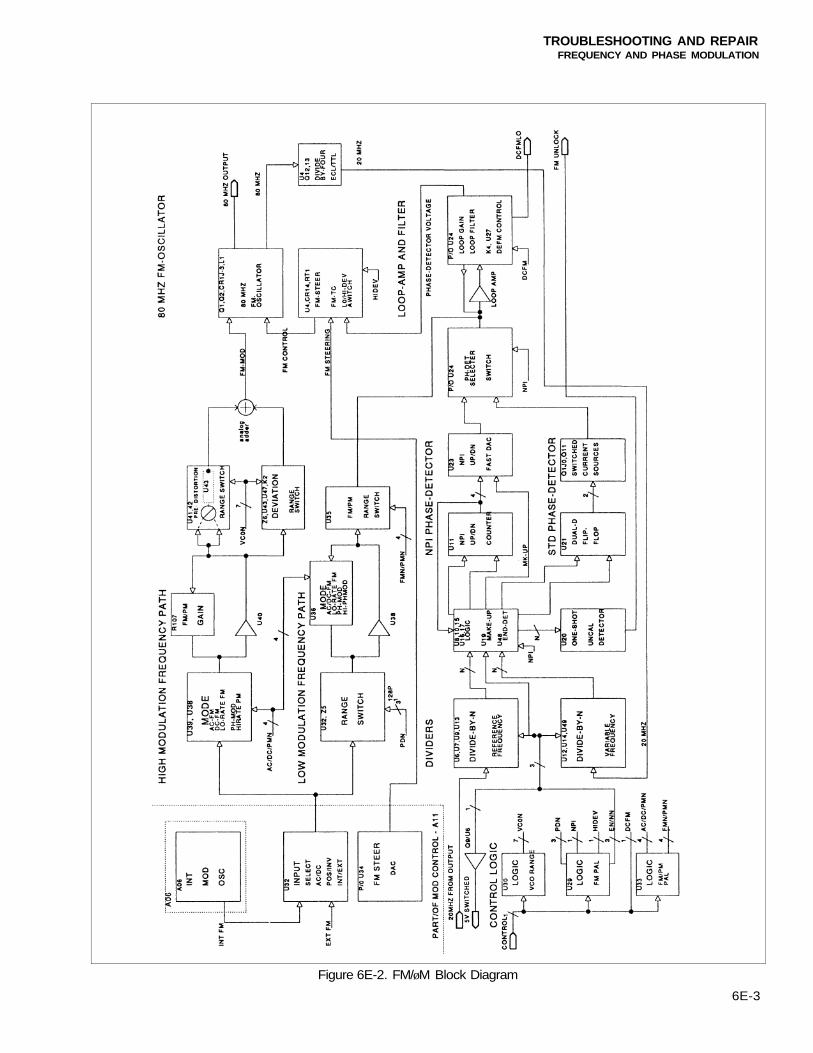
TROUBLESHOOTING AND REPAIRFREQUENCY AND PHASE MODULATION
Figure 6E-2. FM/øM Block Diagram
6E-3
TROUBLESHOOTING AND REPAIRFREQUENCY AND PHASE MODULATION
The circuits of Q3 and Q4 provide clean power supply voltages of nominal +14V DCand -14V DC, respectively. The circuits of quad op-amp U5 and Q6 and Q7 providesteering for the oscillator in the DC-FM mode of operation. Diode CR14 provides astable voltage reference, which is translated to the required varactor control voltages asrequired. One of the op-amps of U5 with Q6 along with the FM-STEER andV-TC-COMP inputs and also variable resistors R35 and R39 and other resistorsprovide the nominal voltage at Q7 for the correct programmed voltage V-PROG atTP2. This is divided in the resistor string of R40, R41, R74, and R133, along with theloop control voltage PH-DET at TP12 to provide the correct voltage VCO-CONTROLfor correct frequency of the oscillator. The control line HIDEVL is programmed by theinstrument control for either HI DEVIATION or not. The remaining sections of U5provide the temperature compensation signal V-TCCOMP, TP9. RT1 is a temperaturesensitive resistor.
Divider Section 6E-5.
The divider section consists of two programmable divider sections: the referencefrequency divider and the variable frequency divider. The reference frequency dividerconsists of U7, U8, U9, U10, and U13. The variable frequency divider consists of U12,U14, U15, U16, U17, and U49. Each divider section respectively divides the referencyfrequency and the variable frequency by the same division. The divider sections receive20 MHz and divide to one of the following frequencies: 5 MHz, 200 kHz or 50 kHz,which is a division by 4, 100, or 400 from the 20 MHz, or it is 16, 400, or 1600 from the80-MHz FM oscillator. Both dividers are programmed to divide the same by thecontrol logic. Each divider consists of three parts: a divide-by-four section, adivide-by-four section and a divide-by-25 section. Multiplexers U13 and U49 controleach divider section for the correct division. A division by 4 (5 MHz) uses just the firstdivide-by-four. A division by 100 (200 kHz) uses the first divide-by-four and thedivide-by-25. A division by 400 (50 kHz) uses all three divider sections.
Each of the divider sections has different outputs. The reference divider section has twooutputs, a signal called "RSIG" and a signal called "Rck". The variable frequencydivider has three output signals: "VSIG", "Vckl", and "Vck2". The output signals areused to control the phase detectors. The relationship of these signals is shown belowand is discussed in the the following paragraphs. The reference divider also has acircuit, REF ON/OFF SWITCH, part of U6 and Q9, which controls the input 20 MHzthat comes from the output board. The circuit enables the 20 MHz from the outputboard except when DCFM is active. The function of the different outputs from thedividers is shown in Figure 6E-3, and discussed under the heading "Phase Detectors,Loop Circuits, and Logic Section" that follows.
Within the signals of each divider the signal relationship is fixed, for example betweenR & Rck, but the relationship between the RSIG signals and the VSIG signals can varyin timing as shown by the first and second set of pulses. These signal drive the phasedetectors as will be discussed in the following paragraphs.
Phase Detectors, Loop Circuits, and Logic Section. 6E-6.
Only one of two phase detectors is active at any time. One of these, U21, is the normal,standard dual D-flip-flop. The other, U11, is a wide range, N-PI phase detector whichuses U11, an up-down counter. The standard phase detector uses diode switchedresistor current sources; the other, the N-PI, uses a switched DAC. Also associatedwith the dividers and phase detectors is an unlock detector, U20, which will respond ifan overmodulation or unlocked condition exists at the phase detector dividercombination.
6E-4
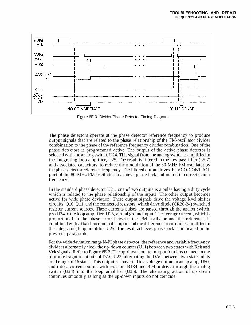
TROUBLESHOOTING AND REPAIRFREQUENCY AND PHASE MODULATION
Figure 6E-3. Divider/Phase Detector Timing Diagram
The phase detectors operate at the phase detector reference frequency to produceoutput signals that are related to the phase relationship of the FM-oscillator dividercombination to the phase of the reference frequency divider combination. One of thephase detectors is programmed active. The output of the active phase detector isselected with the analog switch, U24. This signal from the analog switch is amplified inthe integrating loop amplifier, U25. The result is filtered in the low-pass filter (L5-7)and associated capacitors, to reduce the modulation of the 80-MHz FM oscillator bythe phase detector reference frequency. The filtered output drives the VCO-CONTROLport of the 80-MHz FM oscillator to achieve phase lock and maintain correct centerfrequency.
In the standard phase detector U21, one of two outputs is a pulse having a duty cyclewhich is related to the phase relationship of the inputs. The other output becomesactive for wide phase deviation. These output signals drive the voltage level shiftercircuits, Q10, Q11, and the connected resistors, which drive diode (CR20-24) switchedresistor current sources. These currents pulses are passed through the analog switch,p/o U24 to the loop amplifier, U25, virtual ground input. The average current, which isproportional to the phase error between the FM oscillator and the reference, iscombined with a fixed current in the input, and the difference in current is amplified inthe integrating loop amplifier U25. The result achieves phase lock as indicated in theprevious paragraph.
For the wide deviation range N-PI phase detector, the reference and variable frequencydividers alternately clock the up-down counter (U11) between two states with Rck andVck signals. Refer to Figure 6E-3. The up-down counter output four bits connect to thefour most significant bits of DAC U23, alternating the DAC between two states of itstotal range of 16 states. This output is converted to a voltage output in an op amp, U50,and into a current output with resistors R134 and R94 to drive through the analogswitch (U24) into the loop amplifier (U25). The alternating action of up downcontinues smoothly as long as the up-down inputs do not coincide.
6E-5
TROUBLESHOOTING AND REPAIRFREQUENCY AND PHASE MODULATION
To prevent coincidence problems from occurring, an approaching coincidencecondition is detected with one part of the OVERLAP PULSE AND COINCIDENCEdetector, U19, using the divider outputs "RSIG" and "VSIG". The "RSIG" inputconnects to the "D" input of a first D flip-flop and "V" connects to the clock input ofthe same flip-flop. This sets up the flip-flop and Vckl/Vck2 switch, U18, so that thesecond flip-flop, U19 will make an overlap pulse, clocked by signal "Vck1" and reset bysignal "Vck2" to drive the DAC least significant bits. The switch U18 causes theup-down counter to use the second "V" clock ("Vck2" instead of "Vck1") for clocking,causing a missing portion. The overlap pulse, which occurs at the time between the"Vck1" and "Vck2" clock signals, just fills in for the missing portion. The smoothingadjustment R88 is used to make up for inaccuracies of timing and lower order DAC bitsubstitution.
The up-down counter is prevented from wrapping around from either high to low orlow to high by end-count detectors U48, p/o U10, and p/o U16 inverters, andfour-input NAND gates that control the appropriate clock inputs. This controlinformation is also used to determine overmodulation or an unlocked loop condition.This information is passed to the uncal detector.
The uncal detector U20 receives these inputs and the inputs from the other phasedetector. When the phase detectors are close enough to the edge of normal operation,this will trigger the uncal one-shot, U20, which will stretch out the time of abnormalindication. The output, FM UNLCK, is sent to the instrument controller.
Following the phase detectors is the loop amplifier U25, which, in combination withthe analog switch, selects the appropriate phase detector and gain resistors, R66 andR87, to control the phase-locked bandwidth. The circuit is followed by the loop filter,which has rejection notches at 50 kHz, 90 kHz, and 200 kHz. This filter rejectionreduces the pulses from the phase detectors to maintain minimum spurious modulationof the FM oscillator.
Also associated with the loop amplifier and loop filter are a comparator (U27) and arelay (K4), which are used in DCFM mode of operation of the FM PCA.
The operation to enable DCFM is under control of the instrument controller. Thecontroller operation is as follows:
1. Set up normal ACFM, except disconnect input modulation signals.
2. Monitor comparator output, DCFMLO.
3. Adjust FM STEER DAC on Modulation Control PCA (All), using anappropriate algorithm until the comparator senses nearly zero voltage at TP12.Repeat as necessary.
4. When satisfied, assert the DCFMH control that closes the relay K4, puts TP12 at0V DC ground, and disables dividers and phase lock, and disconnects phasemodulation path. The input modulation signals are reconnected through a DCpath.
ICs U29, U30, and U33 generate the control signals for the rest of the circuits for thedifferent ranges of modulation and the different modes of operation in FM, øM, andDCFM. The inputs are the control lines from the instrument controller, and theoutputs control the divider, phase detector, oscillator, and modulation circuits. See theModulation Control Table (Table 6E-1) for the relationship.
6E-6
TROUBLESHOOTING AND REPAIRFREQUENCY AND PHASE MODULATION
Modulation Section 6E-7.
The modulation section consists of a high rate modulation path and a low ratemodulation path. The modulation signal comes from the Modulation Control PCA atJ6. The signal frequency at this point can range from DC to 200 kHz. Full scaleamplitude for each range is 4V AC-peak for full deviation at the modulationfrequency. The type of modulation is determined following this point. The logiccontrol signals for range switching and type of modulation are generated in the two"PAL" ICs, U29 and U33 and selector U30. This was pointed out previously under theheading "Phase Detector, Loop Circuits, and Logic Section". See Tables 6E-1 and6E-2.
The high rate path consists of U37, U39, U40, U41, U42, U43, U45, U46, U47, K2, andZ6. U37, U45 and U46 are level translators from TTL (CMOS) level to the drive levelfor the analog FET (or DMOS) switches which require levels for "off" of nominal -12VDC and for "on" of +12V DC. The Mode switch for ACFM, DCFM (as well asLow-rate FM), PHMOD (normal), and High-rate PHMOD is U39. This switchfunctions as a one-of-four selector on the input of an amplifier, U40. The adjustments,R104 and C75, are used to balance the different modes of operation. The feedbackresistors, R107 and R108, around this amplifier determine the gain of this path. Theamplifier output drives the range resistor network Z6 and range switches. The rangeswitches are relay switch K2 and analog switches U47 and part of U43. These arecontrolled by level translators U45 and U46. The modulation signal is also amplifiedby U41, which drives a analog multiplier, U42, to generate a second harmonic. Thesecond harmonic is added to the fundamental modulation signal for predistorting thesignal to the modulation port of the 80-MHz VCO. This predistortion cancels thedistortion of the VCO. The analog switches in U43, along with the associated resistors,control and adjust the correct amount of predistortion for each range. The output ofthe range network and switches and the output of the predistortion network are addedin the summing resistors R126 and R127. The relay K1 shorts out the large resistor,R127, for the low deviation ranges (high "Q" mode). The 49.9 ohm resistor R126 is forlow noise performance. The ranges are labeled for FM modulation; however, there arecorresponding phase modulation ranges, i.e., 4 MHz, is 400 (40) radians, etc. Therange and predistortion paths are interactive and require interactive adjustment foreach range; range match: R139, R140, or R141, distortion match: R115, R117, or R119respectively.
The high rate modulation signal and some of the range control logic signals are sent tothe Sum Loop PCA to maintain correct operation there. Since this causes aninteraction between the Sum Loop and the FM PCA, a lead-lag compensation is madewith R120 and C99 controlled by analog switch Q15 and translator U45. The lead-lagcompensation is controlled by the range bit FMRN2H.
The low rate modulation path consists of Z7, U32, U38, U36, Z5, and U35 andassociated components. This path operates in all modes of modulation except in theDCFM mode and the CW mode. The modulation range is determined by a range,network and switch, Z7 and U32, in conjunction with a range network and switch, Z5and U35, relative to the reference frequency. The modulation signal is applied to therange resistor network Z7, selected by analog switch U32, and applied to the virtualground input of a first section of dual op-amp U38. The selected feedback networkdetermines the gain and function. The output of the first op-amp U38 is processed bythe range network Z5 and a range switch U35. The resistors R102 and R145 determinethe gain of the low rate path for ACFM and PHASE-MOD respectively. The selectedfeedback network consists of capacitors and resistors: C70 and R95 for ACFM, R98and C71 for PHASE-MOD, and R146, R147, and C76 for high rate PHASE-MOD.
6E-7
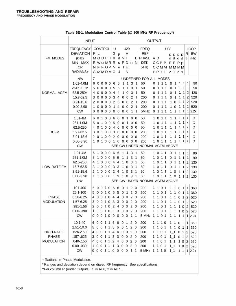
TROUBLESHOOTING AND REPAIRFREQUENCY AND PHASE MODULATION
Table 6E-1. Modulation Control Table (@ 800 MHz RF Frequency*)
6E-8
FM MODES
NORMAL ACFM
DCFM
LOW-RATE FM
PHASEMODULATION
HIGH-RATEPHASE
MODULATION
INPUT
FREQUENCYDEVIATION
(kHz)MIN - MAX
ORRADIANS+
N/A1.01-4.0M251K-1.0M62.5-250k15.7-62.53.91-15.60.00-3.90
CW
1.01-4M251-1.0M62.5-25015.7-62.53.91-15.60.00-3.90
CW
1.01-4M251-1.0M62.5-25015.7-62.53.91-15.60.00-3.90
CW
101-40025.1-1006.26-6.251.57-6.25.391-1.560.00-.390
CW
10.1-402.51-10.0.626-2.50.157-.625.040-.1560.00-.039
CW
CONTROLFMRNG
L0WFM
DcFM
PMOD
HRPM
OUTPUT
U30RNG
U29
pdse1
NPI
HIDEV
nEN
FREQREF
PHASEDET.(kHz)
U33
ACCP
DCCP
PM0
PM1
pdFM2
pdFM1
pdPM2
pdpM1
LOOPR
†
BW(Hz)
7 UNDEFINED FOR ALL MODES6543210
654321
0000000
000000
0000000
111111
0000000
000000
0000000
000000
6543210
654321
6544540
000000
1110000
000000
1100000
110000
3332221
000000
1111111
000000
5050502002002005MHz
505050200200200
0000000
111111
1111111
000000
1111111
111111
1111111
111111
0000111
111111
1111001
111111
1111111
111111
1111111
111111
1122221
XXXXXX
9090
1305205205202.2k
XXXXXX
SEE CW UNDER NORMAL ACFM ABOVE
654321
111111
000000
000000
000000
654321
654343
111111
110000
333333
111111
505050505050
111111
000000
111111
111111
000011
111100
111111
111111
112222
9090
130130130130
SEE CW UNDER NORMAL ACFM ABOVE
6543210
6543210
0000000
0000000
0000000
0000000
1111111
1111111
0000000
1111111
6543210
6543210
6543430
6543430
0000000
0000000
1100000
1100000
2222221
2222221
0000001
0000001
2002002002002002005 MHz
2002002002002002005 MHz
1111111
1111111
1111111
1111111
0000000
1000001
1111111
0111110
1111111
111_11_11_11_11_1
1111111
11
0000111
0000111
1111001
1111001
1122221
1122221
3603605205205205202.2k
3603605205205205202.2k
+ Radians in Phase Modulation.* Ranges and deviation depend on dialed RF frequency. See specifications.†For column R (under Outputs), 1 is R66, 2 is R87.
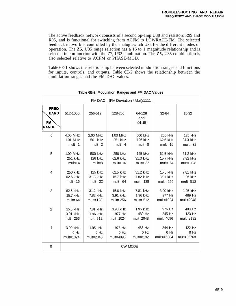
TROUBLESHOOTING AND REPAIRFREQUENCY AND PHASE MODULATION
The active feedback network consists of a second op-amp U38 and resistors R99 andR95, and is functional for switching from ACFM to LOWRATE-FM. The selectedfeedback network is controlled by the analog switch U36 for the different modes ofoperation. The Z5, U35 range selection has a 16 to 1 magnitude relationship and isselected in conjunction with the Z7, U32 combination. The Z5, U35 combination isalso selected relative to ACFM or PHASE-MOD.
Table 6E-1 shows the relationship between selected modulation ranges and functionsfor inputs, controls, and outputs. Table 6E-2 shows the relationship between themodulation ranges and the FM DAC values.
Table 6E-2. Modulation Ranges and FM DAC Values
6E-9
FM DAC = (FM Deviation * Mult)/1111
6
5
4
3
2
1
0
512-1056
4.00 MHz1.01 MHz
mult= 1
1.00 MHz251 kHzmult= 4
250 kHz62.6 kHzmult= 16
62.5 kHz15.7 kHzmult= 64
15.6 kHz3.91 kHz
mult= 256
3.90 kHz0 Hz
mult=1024
256-512
2.00 MHz501 kHzmult= 2
500 kHz126 kHz
mult=8
125 kHz31.3 kHzmult= 32
31.2 kHz7.82 kHz
mult=128
7.81 kHz1.96 kHz
mult=512
1.95 kHz0 Hz
mult=2048
128-256
1.00 MHz251 kHzmult 4
250 kHz62.6 kHzmult= 16
62.5 kHz15.7 kHzmult= 64
15.6 kHz3.91 kHz
mult= 256
3.90 kHz977 Hz
mult= 1024
976 Hz0 Hz
mult=4096
64-128and
.01-15
500 kHz126 kHzmult= 8
125 kHz31.3 kHzmult= 32
31.2 kHz7.82 kHz
mult= 128
7.81 kHz1.96 kHz
mult= 512
1.95 kHz489 Hz
mult=2048
488 Hz0 Hz
mult=8192
32-64
250 kHz62.6 kHzmult= 16
62.5 kHz15.7 kHzmult= 64
15.6 kHz3.91 kHz
mult= 256
3.90 kHz977 Hz
mult=1024
976 Hz245 Hz
mult=4096
244 Hz0 Hz
mult=16384
15-32
125 kHz31.3 kHzmult= 32
31.2 kHz7.82 kHz
mult= 128
7.81 kHz1.96 kHz
mult=512
1.95 kHz489 Hz
mult=2048
488 Hz123 Hz
mult=8192
122 Hz0 Hz
mult=32768
CW MODE
TROUBLESHOOTING AND REPAIRFREQUENCY AND PHASE MODULATION
MODULATION CONTROL CIRCUIT DESCRIPTION 6E-8.
The following description applies only to the FM modulation circuitry on theModulation Control PCA (A11), which is covered in three parts:
• FM input voltage processing.• FM STEER and SUN STEER voltage generation.• FM control signals generation.
FM Input Voltage Processing 6E-9.
The circuits in the list below serve to select and amplify the external FM input signaland the internal mod oscillator signal from a level of 1V AC-peak to a level of 4VAC-peak at the top of each FM range (4 MHz, 1 MHz, etc.), and to provide a vernieroutput within each range as the multiplying DAC is programmed by the controller.
• Op Amp U27• Associated input resistors, capacitors, and CMOS switches, U39• DAC p/o U34 and Op Amp U9A• Inverter/amp U9B
The selection of combinations of EXTAC FM or EXTDC FM and INT FM inputs ismade with the CMOS switches in U39 with its associated resistors and capacitors at theinput of Op-Amp U27. The resistor R82 sets the gain so that a 1 V AC-peak signal isamplified to 4V AC-peak. The FM DEV DAC p/o U34-l,2 is set to 3600 counts (out of4096 at full scale). The FM DEV DAC and op amp U9A produces 4V AC-peak to theinverter/amplifier circuit U9B, which in conjunction with CMOS switch Q6 eitheramplifies directly or inverts the signal to produce the proper output polarity. Thisaccommodates the instrument action of either over or under programming at the sumloop. The multiplying FM DEV DAC U34 (p/o) is under controller operation toproduce a vernier output within each range, or over-range in fixed range, or variationof nominal reference of 3600 counts (out of 4096) for closed-case calibration.
The comparators U16C and U16D with associated resistors serve to trigger one-shotsU26A and U26B to provide information that the applied external level has a peakamplitude centered around 1V AC-peak. The controller responds to deviation from 1VAC-peak to alert the operator with front panel indicators for a "HI" or "LO"indication.
FM Steer Voltage Generation 6E-10.
The FM Steer signal is derived in DAC, p/o U32, and op amp U36B, and rangesbetween 0 and 10.2 V DC (nominally 5.1V DC). The variable resistor R101 is used toadjust this range. The level is under control of the controller for zeroing the frequencyoffset in DCFM.
FM Control Signals Generation 6E-11.
The control signals for the FM OSC PCB (A14) are sent by the controller and latchedin U35. The signals are:
• Three Range switches: FMRN2H, FMRN1H, and FMRN0H.• Four controls: DCFMH, LOWFMH, PMODH, and HRPMH.
6E-10
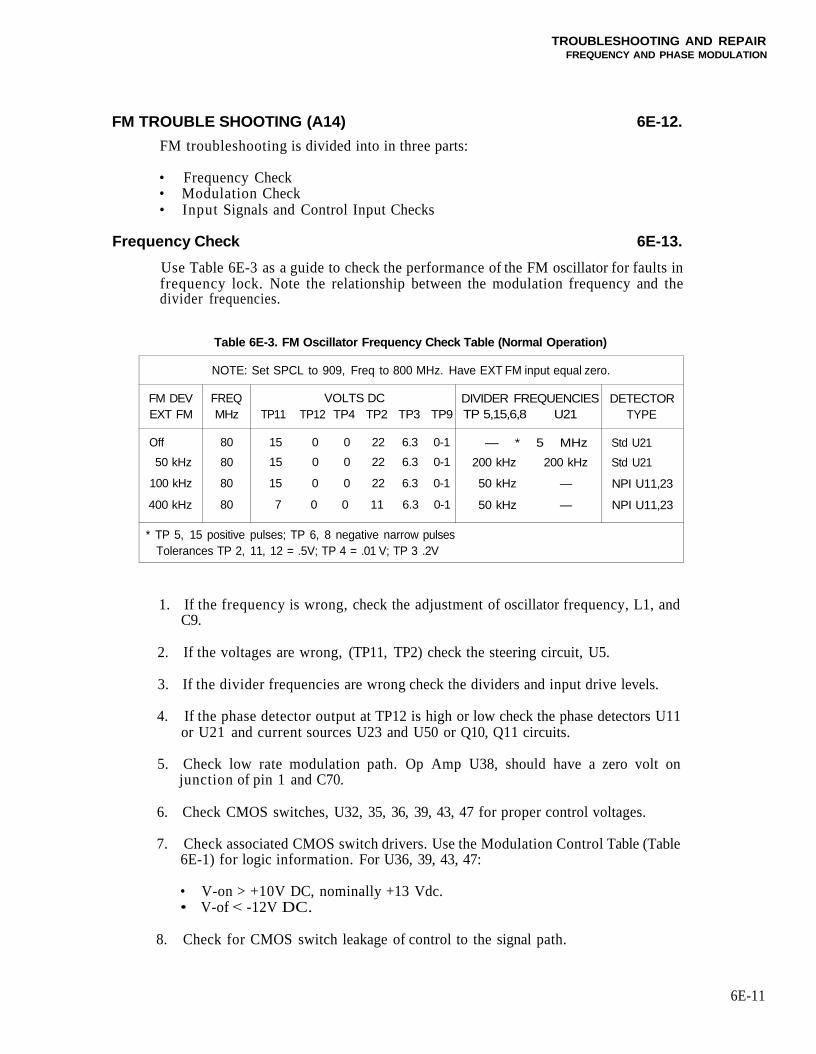
TROUBLESHOOTING AND REPAIRFREQUENCY AND PHASE MODULATION
FM TROUBLE SHOOTING (A14) 6E-12.
FM troubleshooting is divided into in three parts:
• Frequency Check• Modulation Check• Input Signals and Control Input Checks
Frequency Check 6E-13.
Use Table 6E-3 as a guide to check the performance of the FM oscillator for faults infrequency lock. Note the relationship between the modulation frequency and thedivider frequencies.
Table 6E-3. FM Oscillator Frequency Check Table (Normal Operation)
NOTE: Set SPCL to 909, Freq to 800 MHz. Have EXT FM input equal zero.
FM DEVEXT FM
Off
50 kHz
100 kHz
400 kHz
FREQMHz
80
80
80
80
VOLTS DCTP11 TP12 TP4 TP2 TP3 TP9
15 0 0 22 6.3 0-1
15 0 0 22 6.3 0-1
15 0 0 22 6.3 0-1
7 0 0 11 6.3 0-1
DIVIDER FREQUENCIESTP 5,15,6,8 U21
— * 5 MHz
200 kHz 200 kHz
50 kHz —
50 kHz —
DETECTORTYPE
Std U21
Std U21
NPI U11,23
NPI U11,23
* TP 5, 15 positive pulses; TP 6, 8 negative narrow pulsesTolerances TP 2, 11, 12 = .5V; TP 4 = .01 V; TP 3 .2V
1. If the frequency is wrong, check the adjustment of oscillator frequency, L1, andC9.
2. If the voltages are wrong, (TP11, TP2) check the steering circuit, U5.
3. If the divider frequencies are wrong check the dividers and input drive levels.
4. If the phase detector output at TP12 is high or low check the phase detectors U11or U21 and current sources U23 and U50 or Q10, Q11 circuits.
5. Check low rate modulation path. Op Amp U38, should have a zero volt onjunction of pin 1 and C70.
6. Check CMOS switches, U32, 35, 36, 39, 43, 47 for proper control voltages.
7. Check associated CMOS switch drivers. Use the Modulation Control Table (Table6E-1) for logic information. For U36, 39, 43, 47:
• V-on > +10V DC, nominally +13 Vdc.• V-of < -12V DC.
8. Check for CMOS switch leakage of control to the signal path.
6E-11
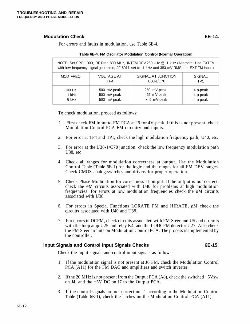
TROUBLESHOOTING AND REPAIRFREQUENCY AND PHASE MODULATION
Modulation Check 6E-14.
For errors and faults in modulation, use Table 6E-4.
Table 6E-4. FM Oscillator Modulation Control (Normal Operation)
NOTE: Set SPCL 909, RF Freq 800 MHz, INTFM DEV 250 kHz @ 1 kHz (Alternate: Use EXTFMwith low frequency signal generator, JF 6011 set to 1 kHz and 383 mV RMS into EXT FM input.)
MOD FREQ
100 Hz1 kHz5 kHz
VOLTAGE ATTP4
500 mV-peak500 mV-peak500 mV-peak
SIGNAL AT JUNCTIONU38-1/C70
250 mV-peak25 mV-peak< 5 mV-peak
SIGNALTP1
4 p-peak4 p-peak4 p-peak
To check modulation, proceed as follows:
1. First check FM input to FM PCA at J6 for 4V-peak. If this is not present, checkModulation Control PCA FM circuitry and inputs.
2. For error at TP4 and TP1, check the high modulation frequency path, U40, etc.
3. For error at the U38-1/C70 junction, check the low frequency modulation pathU38, etc
4. Check all ranges for modulation correctness at output. Use the ModulationControl Table (Table 6E-1) for the logic and the ranges for all FM DEV ranges.Check CMOS analog switches and drivers for proper operation.
5. Check Phase Modulation for correctness at output. If the output is not correct,check the øM circuits associated with U40 for problems at high modulationfrequencies; for errors at low modulation frequencies check the øM circuitsassociated with U38.
6. For errors in Special Functions LORATE FM and HIRATE, øM check thecircuits associated with U40 and U38.
7. For errors in DCFM, check circuits associated with FM Steer and U5 and circuitswith the loop amp U25 and relay K4, and the LODCFM detector U27. Also checkthe FM Steer circuits on Modulation Control PCA. The process is implemented bythe controller.
Input Signals and Control Input Signals Checks 6E-15.
Check the input signals and control input signals as follows:
1. If the modulation signal is not present at J6 FM, check the Modulation ControlPCA (A11) for the FM DAC and amplifiers and switch inverter.
2. If the 20 MHz is not present from the Output PCA (A8), check the switched +5Vswon J4, and the +5V DC on J7 to the Output PCA.
3. If the control signals are not correct on J1 according to the Modulation ControlTable (Table 6E-1), check the latches on the Modulation Control PCA (A11).
6E-12
TROUBLESHOOTING AND REPAIRFREQUENCY AND PHASE MODULATION
FM ADJUSTMENTS 6E-16.
This alignment includes the following PCAs:
• A11, 6080A/AN-4048 MOD CONTROL, The FM modulation section• A14, 6080A/AN-4045 FM Oscillator
The following equipment is recommended to make FM adjustments:
DMM (Fluke 8840A)Modulation meter (HP 8901A)LFSSG (Fluke 6011A)Spectrum analyzer (HP 8586)Oscilloscope (Tektronix)
Adjustments on the Modulation Control PCA (A11) 6E-17.
NOTE
This procedure concerns the adjustment of the modulation circuitry.Other adjustments are covered in other procedures.
Make adjustments on the Modulation Control PCA as described in the followingprocedure:
1. Make the following equipment settings:
a. Set the UUT to SPCL 909, 800 MHz, 0 dBm, 4 MHz dev, EXT ACFM.
b. Set the 8840A DMM to AC volts, autorange.
c. Set the 6011A Signal Generator to 1 kHz, 383 mV RMS.
2. Connect the 6011A to the UUT EXT FM input and to the 8840A.
3. Set the 6011A (as measured by the 8840A) to 707 mV RMS. Set the 8840A to ACvolts, and autorange. Connect the 8840A to J16-P1 on 4048 Modulation ControlPCA. Adjust R82 for 2.828V RMS ± 2 mV.
4. Set the UUT to 700 MHz. Set the 8840A to AC volts, autorange. Connect the8840A to J16-P1 on 4048 Modulation Control PCA. Adjust R102 for a reading of2.828V RMS ± 2 mV on the 8840A.
5. Set the UUT EXT ACFM off and set the UUT INT FM on. The 8840A should read2.828V RMS ± 2 mV RMS.
Set UUT INT FM off and set UUT EXT ACFM on.
6. Set the UUT to SPCL 943. Connect the 8840A to J2-P14. Set the 8840A to DCvolts. Adjust R99 for 10.24V DC ± 10 mV.
Connect the 8840A to J1-P3. Set the 8840A to DC volts. Adjust R101 for 10.24VDC ± 10 mV.
Connect 8840A to J6-P24. Verify that the 8840A reads 10V DC ± .1V DC.
6E-13
TROUBLESHOOTING AND REPAIRFREQUENCY AND PHASE MODULATION
7. Set the UUT to SPCL 909. Connect a 50-ohm termination to UUT EXT PULSEMOD. Connect the 8840A to J4-P5. The 8840A should read 0V DC ± .2V DC.Press the External Pulse Modulation button on UUT front panel to on. The 8840Ashould read 4.2V DC ± .2V DC.
8. Set the UUT to SPCL 909. Set the 8840A to DC volts, 2-volt range. Connect the8840A to TP1 on the 4048 board. Adjust the modulation level sense R71 for .98V ±.5 mV. Remove 8840A from TP1.
9. Set the UUT to EXT FM. Set the 6011A to 1 kHz and 383 mV. Connect the 6011Aand the 8840A to the UUT FM EXT input.
a. Edit the 6011A level until the 8840A reads .707V RMS. Verify on the UUTfront panel that the EXT FM LO and the FM HI annunciators are off.
b. Increase the 6011A output voltage to .728V RMS as measured on the 8840A.Verify that the EXT FM HI annunciator is on.
c. Decrease the 6011A output voltage to .685V RMS as measured on the 8840A.Verify that the EXT FM LO annunciator is on.
10. Set UUT to SPCL 909, EXT AM. Set the 6011A to 1 kHz and 383 mV. Connect the6011A and the 8840A to the UUT AM EXT input.
a. Edit the 6011A level until the 8840A reads .707V RMS. Verify on the UUTfront panel that the EXT AM LO and the AM HI annunciators are off.
b. Increase the 6011A output voltage to .728V RMS as measured on the 8840A.Verify that the EXT AM HI annunciator is on.
c. Decrease the 6011A output voltage to .685V RMS as measured on the 8840A.Verify that the EXT AM LO annunciator is on.
Alignment of FM PCA (A14) 6E-18.
Align the FM PCA as described in the following procedure:
1. Center all pots on the FM PCA. Turn the UUT off. Set the 6011A to 50 kHz at 0dbm. Connect the 6011A to TP12. Connect the spectrum analyzer to TP11. AdjustL6 for a minimum 50-kHz level. Remove the 6011A and the analyzer.
2. Set the UUT to SPCL 909, 800 MHz, 62.5-kHz dev, 1-kHz mod rate, INT ACFM.Set the 8840A to AC volts, autorange. Connect the 8840A to TP1 on the FM PCA.Adjust R107 for 2.828V RMS ± 2 mV RMS. Turn INT ACFM off.
3. Remove the cap from J3 to J17 connecting the FM PCA to the Sum Loop PCA(A12). Connect the counter to J3. Adjust L1 to be flush to the top of its housing.Adjust C9 for a locked 80 MHz as read on the counter.
4. Remove the counter from J3 and connect 436A to J3. Adjust R45 for -5 dBm ± . 1dB. Disconnect 436A from J3. Install the 1000 pF cap from J3 to J17 on the SumLoop PCA.
5. Connect the 8840A to TP9. Set the 8840A to DC volts. Adjust R44 for 0V DC ± 10mV DC.
6E-14
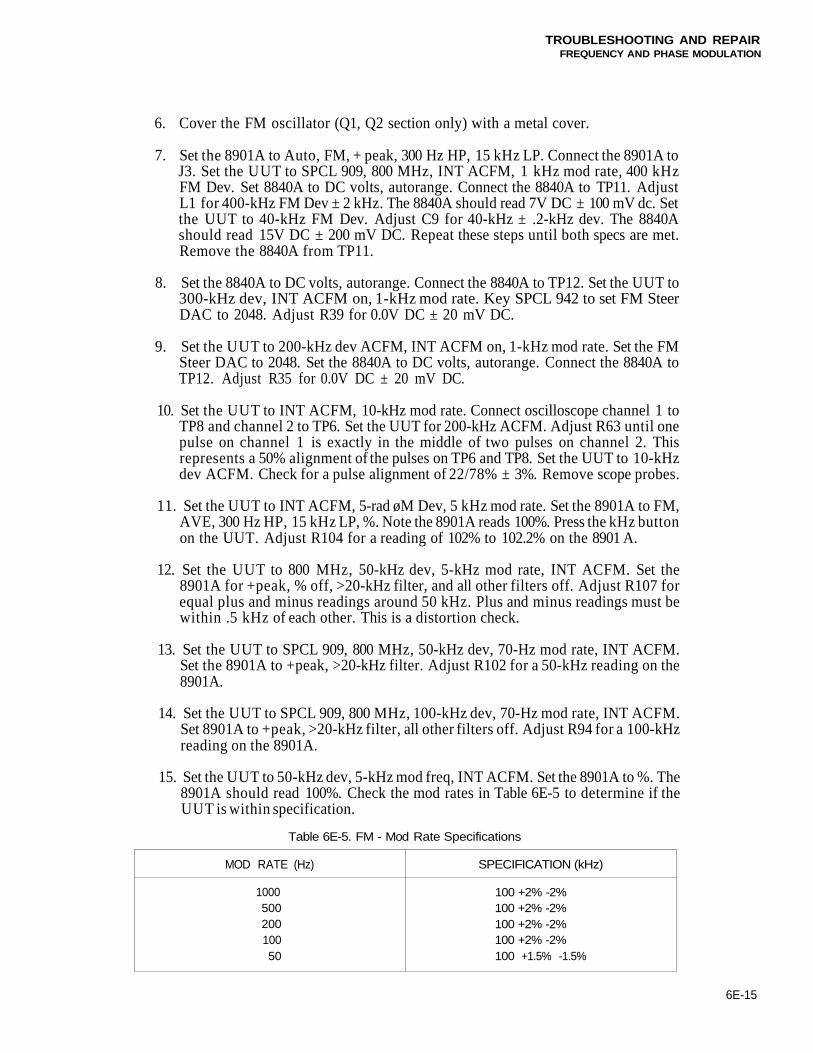
TROUBLESHOOTING AND REPAIRFREQUENCY AND PHASE MODULATION
6. Cover the FM oscillator (Q1, Q2 section only) with a metal cover.
7. Set the 8901A to Auto, FM, + peak, 300 Hz HP, 15 kHz LP. Connect the 8901A toJ3. Set the UUT to SPCL 909, 800 MHz, INT ACFM, 1 kHz mod rate, 400 kHzFM Dev. Set 8840A to DC volts, autorange. Connect the 8840A to TP11. AdjustL1 for 400-kHz FM Dev ± 2 kHz. The 8840A should read 7V DC ± 100 mV dc. Setthe UUT to 40-kHz FM Dev. Adjust C9 for 40-kHz ± .2-kHz dev. The 8840Ashould read 15V DC ± 200 mV DC. Repeat these steps until both specs are met.Remove the 8840A from TP11.
8. Set the 8840A to DC volts, autorange. Connect the 8840A to TP12. Set the UUT to300-kHz dev, INT ACFM on, 1-kHz mod rate. Key SPCL 942 to set FM SteerDAC to 2048. Adjust R39 for 0.0V DC ± 20 mV DC.
9. Set the UUT to 200-kHz dev ACFM, INT ACFM on, 1-kHz mod rate. Set the FMSteer DAC to 2048. Set the 8840A to DC volts, autorange. Connect the 8840A toTP12. Adjust R35 for 0.0V DC ± 20 mV DC.
10. Set the UUT to INT ACFM, 10-kHz mod rate. Connect oscilloscope channel 1 toTP8 and channel 2 to TP6. Set the UUT for 200-kHz ACFM. Adjust R63 until onepulse on channel 1 is exactly in the middle of two pulses on channel 2. Thisrepresents a 50% alignment of the pulses on TP6 and TP8. Set the UUT to 10-kHzdev ACFM. Check for a pulse alignment of 22/78% ± 3%. Remove scope probes.
11. Set the UUT to INT ACFM, 5-rad øM Dev, 5 kHz mod rate. Set the 8901A to FM,AVE, 300 Hz HP, 15 kHz LP, %. Note the 8901A reads 100%. Press the kHz buttonon the UUT. Adjust R104 for a reading of 102% to 102.2% on the 8901 A.
12. Set the UUT to 800 MHz, 50-kHz dev, 5-kHz mod rate, INT ACFM. Set the8901A for +peak, % off, >20-kHz filter, and all other filters off. Adjust R107 forequal plus and minus readings around 50 kHz. Plus and minus readings must bewithin .5 kHz of each other. This is a distortion check.
13. Set the UUT to SPCL 909, 800 MHz, 50-kHz dev, 70-Hz mod rate, INT ACFM.Set the 8901A to +peak, >20-kHz filter. Adjust R102 for a 50-kHz reading on the8901A.
14. Set the UUT to SPCL 909, 800 MHz, 100-kHz dev, 70-Hz mod rate, INT ACFM.Set 8901A to +peak, >20-kHz filter, all other filters off. Adjust R94 for a 100-kHzreading on the 8901A.
15. Set the UUT to 50-kHz dev, 5-kHz mod freq, INT ACFM. Set the 8901A to %. The8901A should read 100%. Check the mod rates in Table 6E-5 to determine if theUUT is within specification.
Table 6E-5. FM - Mod Rate Specifications
6E-15
MOD RATE (Hz)
100050020010050
SPECIFICATION (kHz)
100 +2% -2%100 +2% -2%100 +2% -2%100 +2% -2%100 +1.5% -1.5%
TROUBLESHOOTING AND REPAIRFREQUENCY AND PHASE MODULATION
16. Set the UUT to SPCL 909, 800 MHz, 150-kHz dev, 25-Hz mod rate, INT ACFM.Connect the oscilloscope to the 8901A MOD OUT. Adjust the scope for almostfull scale display with one cycle. Adjust R88 for a smooth waveform.
17. Set the UUT to 800 MHz, 5-kHz mod rate, 200-kHz dev, INT ACFM. Set the8901A to FM, + peak, 300 Hz HP, 15 kHz LP. Adjust R141 for a 8901A reading of200 kHz ± 1 kHz. Adjust R119 for symmetrical plus and minus readings about 200kHz ± 1 kHz.
Repeat until both specs are met.
18. Set the UUT to 200 MHz, 5-kHz mod rate, 200-kHz dev, INT ACFM. Set the8901A to FM, + peak, 300 Hz HP, 15 kHz LP. Adjust R140 for a 8901A reading of200 kHz ± 1 kHz. Adjust R117 for symmetrical plus and minus readings about 200kHz ± 1 kHz.
Repeat until both specs are met.
19. Set the UUT to 50 MHz, 5-kHz mod rate, 200-kHz dev, INT ACFM. Set the8901A to FM, + peak, 300 Hz HP, 15 kHz LP. Adjust R139 for a 8901A reading of200 kHz ± 1 kHz. Adjust R115 for symmetrical plus and minus readings about 200kHz ± 1 kHz.
Repeat until both specs are met.
20. Set the UUT to 800 MHz, 70-Hz mod rate, 5-rad dev, INT ACFM. Set the 8901Ato øM, + peak, 15 kHz LP (all other filters removed), Avg and 70.7%. Adjust R145for 5 rad.
21. Set the UUT to 800 MHz, 10-kHz mod rate, 5-rad dev, SPCL 721, INT ACFM.Set the 8901A to øM, + peak, 300 Hz HP, >20 kHz LP. Adjust C75 for a 8901Areading of 5 rad.
Set the UUT to 1-kHz mod rate. The 8901A reading must be 5 rad ± .05 rad.
22. Set the UUT to 800 MHz, 70-Hz mod rate, 5-rad dev, SPCL 721, INT ACFM. Setthe 8901A to øM, + peak, no filters, Avg and 70.7%. Adjust R146 for 5 rad. SetUUT to SPCL 720.
23. Connect the 8840A to TP12 and adjust R49 to 0V DC.
Connect the 8840A to TP9. Verify that the 8840A reads between -3V DC and + 10VDC.
24. Set the UUT to SPCL 909, 800 MHz, -5 dBm, mod freq 10 Hz, 25-kHz FMdeviation, SPCL 711, SPCL 752. Set the spectrum analyzer to IP, center freq800.06 MHz, span 100 kHz, ref level -5 dBm, resolution bandwidth 30 kHz, videobandwidth 30 kHz, sweep time 200 ms, log scale 6 dB, trigger free run.
Set the UUT to INT FM. Set analyzer to span 0 Hz, trigger video. Verify that thedroop of the demodulated FM is less than 10%. Set the UUT to EXT DCFM.Verify that the droop of the demodulated DCFM is less than 2%.
6E-16
TROUBLESHOOTING AND REPAIRFREQUENCY AND PHASE MODULATION
25. Set the UUT to 800 MHz, 300-kHz dev, 1-kHz mod rate, EXT ACFM on. Connectthe 8840A to TP12 and check that the 8840A reads 0V DC ± 200 mVdc.
Set the UUT to 200-kHz dev. Check that the 8840A reads 0V DC ± 200 mV DC.
26. Set the UUT to 800 MHz, 10-kHz dev, 1-kHz mod rate, EXT ACFM. Place a600-ohm load on the UUT EXT FM input. Connect 1953A Counter to UUToutput and set the 1953A to read 800 MHz with 1 Hz resolution.
Set the UUT to EXT DCFM. The front panel DCFM indicator should come onwithin one second. The 1953A should read within 350 Hz of the 800 MHz ACFMfrequency. Connect the 8840A to TP12. TP12 should read 0V DC. Connect the8840A to J1-P3. The 8840A should read between 3V DC and 8V DC.
Set the UUT to ACFM. Repeat step 25 to verify performance.
Set the UUT to ACFM.
27. Set the UUT to 300-kHz dev. Set the UUT to EXT DCFM. The front panelDCFM indicator should come on within one second. The 1953A should readwithin 500 Hz of the 800 MHz ACFM frequency. Connect the 8840A to TP12.TP12 should read 0V DC. Connect the 8840A to J1-P3. The 8840A should readbetween 3V DC and 8V DC.
Set the UUT to ACFM. Repeat step 26 to verify performance.
6E-17/6E-18

Section 6FInternal Modulation Oscillator
MODULATION OSCILLATOR BLOCK DIAGRAM 6F-1.
Refer to the Modulation Oscillator Block Diagram (Figure 6F-1) to identify the majorfunctional sections and follow the signal paths of the internal modulation oscillator.
INTERNAL MODULATION OSCILLATOR CIRCUIT DESCRIPTION 6F-2.
The modulation oscillator is configurable as either a direct digital synthesizer (DDS)or as a pulse generator. Both functions are implemented in a custom integrated circuitand are synthesized from the main reference frequency source of the instrument.
The Mod Oscillator PCA provides two outputs:
• An internal modulation source (INT MOD)
• A modulation output source (MOD OUT), which is available at the MODULA-TION OUTPUT BNC connector at the front panel.
All power, data, control and clock signals are received by the Mod Oscillator PCA viaa bus connector (J1) and clock connector (J2). The Mod Oscillator PCA has twooutputs, INT MOD and MOD OUT.
Direct Digital Synthesized Wave Generator 6F-3.
The direct digital synthesizer frequency can be set from 0.1 Hz to 200 kHz withresolution of 0.1 Hz. It is the modulation source for the internal AM, FM, øM, andpulse functions. The amplitude of the internal modulation source (INT MOD signal) isa leveled 1V pk which is internally routed to the Modulation Control PCA (A11). Theamplitude of the modulation output is controlled by a level DAC. The oscillator isbased on an algorithmic wave generation method, which provides a very accurate andstable signal source of high purity and low harmonic distortion. The main function ofthis system is implemented in the custom integrated circuit U1 and it uses an externalwave lookup table (U2, U3), and a 12-bit wave reconstruction DAC (U7 and U9B).Since a discrete time sampled method is employed in generating the various waves, alow pass antialiasing filter, R6, R7, C13, C14, L1, is required to reject the samplingfrequency, the alias signals and the out of band spurious from the output signal.
The amplitude of oscillation at the MODULATION OUTPUT connector is controlledby a 12-bit multiplying DAC (U8, U11A). This output level can be set between 0 to 4Vpk, with 1-mV pk steps, into a 600-ohm load.
6F-1
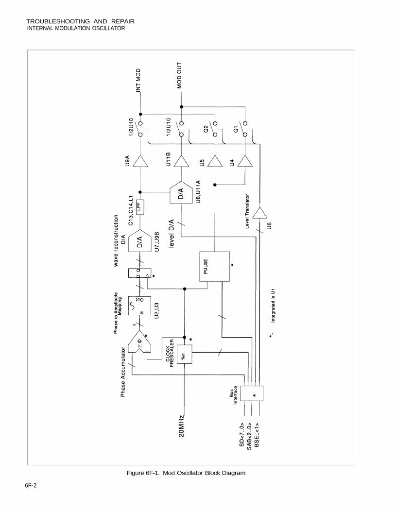
TROUBLESHOOTING AND REPAIRINTERNAL MODULATION OSCILLATOR
6F-2
Figure 6F-1. Mod Oscillator Block Diagram
TROUBLESHOOTING AND REPAIRINTERNAL MODULATION OSCILLATOR
The wave data is stored in two EPROMS (U2, U3). Three control lines from U1control the wave-form selection, allowing up to eight waveforms to be selected via afront panel special function. When a wave other than the sine wave is used,consideration for the low-pass filter cutoff frequency (200 kHz) should be made. Therewill be a progressive deterioration of the fidelity of waves with increased frequency,depending on the wave shape selected. This relates to the higher frequency componentsof the waves other than sine wave.
Pulse Generator 6F-4.
The pulse generation mode is selected via front panel or IEEE Special Functioncommands. The frequency of the pulse generator can be set from 10 Hz to 200 kHz.Frequency and pulse width are determined by numeric values written to the oscillator.The built-in pulse generator can be used as a modulation source for the internal AM,FM, øM and pulse.
The pulse generator is based on the custom IC (U1), which contains a programmableperiod and pulse width sections. Both the period and the width of the pulse can be set inincrements of 100 ns. Internally, the pulse frequency is rounded and set to the nearest100 ns period increment of the entered modulation frequency.
U4, U5, Q1, Q2, and associated components provide conditioning for the external andinternal pulse signals. When in the pulse generation mode of operation, the internalpulse at INT MOD is preset to 1V pk via U5. U4 buffers the pulse output of the customIC (U1) to provide MOD OUT, which is fixed at 4.5V CMOS/TTL logic level. Both,the frequency and the pulse width are set numerically through front panel entry or viaIEEE commands. In pulse generation mode, MOD OUT is terminated with a nominal180 ohms.
To avoid the ambiguity of the pulse output from being set to a DC value, the softwarelimits the pulse width to a value that is no wider than the set period minus 100 ns, and itprevents it from being set narrower than 100 ns.
See the Special Function list in Appendix B for selections modulation oscillator modesof operations. The appropriate Special Functions allow the selection of direct digitalsynthesis, output waveform, pulse generator and pulse width setting. In addition, byselecting the appropriate special function code, it is possible to enable MOD OUT tobe continuously on (default) or to be turned on only during the selection of internalmodulation.
Signal Routing 6F-5.
The modulation oscillator is set up to select the active outputs by means of six analogswitches. Signals from U1 control the various switch functions to route the pulsegenerator and direct digital dynthesizer output signals to the two outputs (INT MOD,MOD OUT) of the Modulation Oscillator PCA.
The two switches associated with U9A, S1, S2, U6A, U6B, facilitate the connection ofthe direct digital synthesizer to the internal modulation source (INT MOD). The twoswitches associated with U11B, S3, S4, U6C, U6D, facilitate the connection of thedirect digital dynthesizer to the modulation output (MOD OUT). The two switchesassociated with U4 and U5, S5, S6, U6B, and U6D facilitate the connection of the pulsegenerator to both the modulation output (MOD OUT) and to the internal modulationsource (INT MOD).
6F-3
TROUBLESHOOTING AND REPAIRINTERNAL MODULATION OSCILLATOR
MOD OSCILLATOR TROUBLESHOOTING AND ADJUSTMENTS 6F-6.
Since both the direct digital synthesizer (DDS) and the pulse generator sections areclocked by the same clock, the first signal to verify is the input 20 MHz. In the absenceof this clock, no function on the assembly will operate. The amplitude of this waveshould be at least 300 mV p-p.
Direct Digital Synthesizer Troubleshooting 6F-7.
To troubleshoot the direct digital synthesizer, proceed as follows:
SETTING UP:
1. Put the UUT into the preset default state by selecting SPCL 909. This sets the DDSto generate a sine wave.
2. Enable INT AM modulation.
3. Set MOD LEV to a modulation output level of 4V pk.
4. Enter MOD FREQ of 1 kHz.
5. Connect a 600-ohm load at the MOD OUTPUT connector.
TEST PROCEDURE:
1. Check U1 output clock CLKO at TP10. This logic level signal should be at 3.33MHz. If there is no signal at this point or the frequency is wrong, either U1 is faulty,wrong data is written to it, or the 20 MHz signal is inadequate. With the absence ofthis signal the DDS sections will not operate.
2. Using an oscilloscope, verify that the most significant bit (MSB) of the phaseaccumulator (TP8) is at TTL level and is at 1 kHz (the set modulation frequency).If the MSB is not as indicated, it is probable that the most significant lookup table(U2) is faulty. Another possibility is that U1 phase accumulator section does notfunction correctly.
3. Next use the oscilloscope to verify the presence of a 10V p-p (±5%) sine wave at theoutput of the wave reconstruction DAC (TP2). If not, suspect the DAC (U7) andthe DAC output amplifier (U9A), or the wave tables (U2, U3). If the signal is notzero centered or the amplitude is in error, check R4 and R5, also verify 10V ±2% atpin 4 of (U7).
4. Verify that a 4.77V p-p ±5% sine wave is present at TP3. If the sine wave is notpresent or is of the wrong amplitude, check the 3-pole low-pass filter components(R6, C13, C14, L1 and R7).
5. Enter MOD FREQ of 100 kHz.
6. Repeat step 4 above.
7. Enter MOD FREQ of 1 kHz.
6F-4
TROUBLESHOOTING AND REPAIRINTERNAL MODULATION OSCILLATOR
8. Using an oscilloscope, check for the presence of a 2V p-p sine wave at TP4 andmeasure its amplitude with an AC voltmeter to verify it is 0.7071V rms within±0.1% (±0.7 mV). If the sine wave is not present or is distorted, check S1, S2(U10), and U9B and associated components. If amplitude is slightly off, recalibrate(R9) using normal calibration procedures.
9. Using an oscilloscope, verify the presence of a 4.66V p-p (±5%) sine wave signal atTP9 and check for visible distortions. If the sine wave is not present, is distorted, oris of the wrong amplitude, check level DAC U8, and U11A. If U8 and U11A areOK, it could be a write data error that could result from a faulty U1 or an interfacebus fault.
10. Using an oscilloscope, verify the presence of a zero centered 8V p-p sine wave atTP5. If the signal is distorted, check U11B and associated resistors (R11, R12,R13) and switches (S3, S4). With an AC voltmeter, check for 2.8284 V rms ±0.1 %(±2.8mV). If the signal not within specified accuracy, recalibrate (R13) usingnormal calibration procedures.
S1-S6 refer to analog switches on the Modulation Oscillator.
Pulse Generator Troubleshooting 6F-8.
To troubleshoot the pulse generator, proceed as follows:
SETTING UP:
1. Put instrument into preset default state by selecting entering SPCL 758.
2. Set up the instrument for internal pulse operation (SPCL 741).
3. Enable INT AM modulation.
4. Enter MOD FREQ of 10 kHz (100 us period).
5. Set the pulse width to 25 us (SPCL 759).
TEST PROCEDURE:
NOTEModulation level control has no effect in pulse mode.
1. Verify the presence of a 10.0-MHz logic signal at TP10. If no signal is present at thispoint or the signal is the wrong frequency, either U1 is faulty, a data write error hasoccurred, or the 20-MHz signal is inadequate.
2. Using an oscilloscope connected to TP11, verify that the TTL level PULSE signalfrom U1, is at 10 kHz and that it has a positive pulse width of 25 us. If not, it isprobable that U1 is faulty.
3. Using an oscilloscope, verify that the TTL level PULSE described in step 2 above ispresent at TP5.
4. Using an oscilloscope to observe TP4, verify that the same pulse shape described instep 2 is zero centered, with an amplitude of 2V ±10% p-p. If either the amplitudeor wave shape is incorrect, check U5 and the associated resistors (R22, R23, R24,R25).
6F-5/6F-6

Section 7List of Replaceable Parts
TABLE OF CONTENTS
ASSEMBLY NAME TABLE PAGE FIGURE PAGENO. NO. NO. NO.
6080A/AN Final Assembly 7-1 7-4 7-1 7-7A1 Display PCA 7-2 7-19 7-2 7-20A2 Coarse Loop PCA 7-3 7-21 7-3 7-25A3 Sub-Synthesizer VCO PCA 7-4 7-26 7-4 7-27A4 Sub-Synthesizer PCA 7-5 7-28 7-5 7-31A5 Coarse Loop VCO PCA 7-6 7-32 7-6 7-33A6 Mod Oscillator PCA 7-7 7-34 7-7 7-35A8 Output PCA 7-8 7-36 7-8 7-39A9 Sum Loop VCO PCA 7-9 7-40 7-9 7-41A10 Premodulator PCA 7-10 7-42 7-10 7-45A11 Modulation Control PCA 7-11 7-46 7-11 7-49A12 Sum Loop PCA 7-12 7-50 7-12 7-53A13 Controller PCA 7-13 7-54 7-13 7-56A14 FM PCA 7-14 7-57 7-14 7-61A15 Power Supply PCA 7-15 7-62 7-15 7-64A16 IEEE-488 Connector PCA 7-16 7-65 7-16 7-66A19 Switch PCA 7-17 7-67A20 Attenuator/RPP Assembly 7-18 7-68
A7 Relay Driver PCA 7-19 7-69 7-17 7-70A21 Attenuator PCA 7-20 7-71 7-18 7-72
7-1
REPLACEMENT PARTS
INTRODUCTION 7-1.
Section 7 contains an illustrated list of replaceable parts for the 6080A/ANSynthesized Signal Generator. Parts are listed alphanumerically by assembly.
The part lists include the following information:
1. Reference Designation
2. Description of each part
3. Fluke Stock Number
4. Federal Supply Code for Manufacturers.
A list of part manufacturers, arranged numerically by Federal Supply Code, isprovided at the end of Section 7.
5. Manufacturer's part number.
6. Total Quantity of components per assembly.
7. Recommended Quantity.
This entry indicates the recommended number of spare parts necessary to supportone to five instruments for a period of 2 years. This list presumes an availability ofcommon electronic parts at the maintenance site. For maintenance for 1 year ormore at an isolated site, it is recommended that at least one of each assembly in theinstrument be stocked.
HOW TO OBTAIN PARTS 7-2.
Components may be ordered directly from the manufacturer by using the manufactur-er's part number, or from John Fluke Mfg. Co. (or its authorized representative) byusing the Fluke stock number.
In the event the part you order has been replaced by a new or improved part, thereplacement will be accompanied by an explanatory note and, if necessary, installationinstructions.
To ensure prompt and efficient handling of your order, include the followinginformation.
1. Quantity.
2. Fluke Stock Number.
3. Description.
4. Reference Designation.
5. Printed Circuit Board Part Number and Revision Letter.
6. Instrument Model and Serial Number.
7-2
REPLACEMENT PARTS
A Recommended Spare Parts Kit for your basic instrument is available from thefactory. This kit contains recommended quantities of those items as listed in the RECQTY column of the parts list.
Price information of parts is available from the John Fluke Mfg. Co., Inc. or itsrepresentative. Prices are also available in the Fluke Replacement Parts Catalog,which is available on request.
SERVICE CENTERS 7-3.
A list of Fluke/Philips technical service centers is provided at the end of Section 7.
CAUTION
Parts preceded by and asterisk (*) are subject to damage by staticdischarge.
7-3
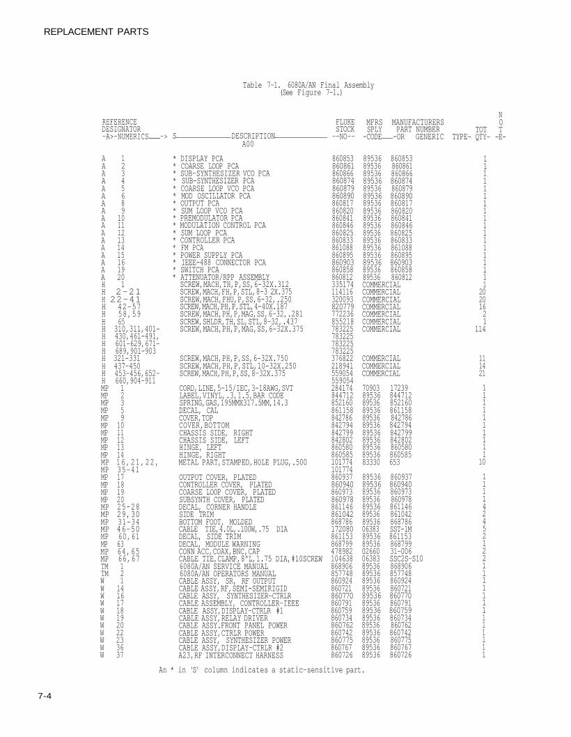
REPLACEMENT PARTS
Table 7-1. 6080A/AN Final Assembly(See Figure 7-1.)
REFERENCEDESIGNATOR-A>-NUMERICS ->
A 1A 2A 3A 4A 5A 6A 8A 9A 10A 11A 12A 13A 14A 15A 16A 19A 20H 1H 2-21H 22-41H 42-57H 58,59H 65H 310,311,401-H 430,461-491,H 601-629,671-H 689,901-903H 321-331H 437-450H 453-456,652-H 660,904-911MP 1MP 2MP 3MP 5MP 9MP 10MP 11MP 12MP 13MP 14MP 16,21,22,MP 35-41MP 17MP 18MP 19MP 20MP 25-28MP 29,30MP 31-34MP 46-50MP 60,61MP 63MP 64,65MP 66,67TM 1TM 2W 1W 14W 16W 17W 18W 19W 20W 22W 23W 36W 37
S DESCRIPTIONA00
* DISPLAY PCA* COARSE LOOP PCA* SUB-SYNTHESIZER VCO PCA* SUB-SYNTHESIZER PCA* COARSE LOOP VCO PCA* MOD OSCILLATOR PCA* OUTPUT PCA* SUM LOOP VCO PCA* PREMODULATOR PCA* MODULATION CONTROL PCA* SUM LOOP PCA* CONTROLLER PCA* FM PCA* POWER SUPPLY PCA* IEEE-488 CONNECTOR PCA* SWITCH PCA* ATTENUATOR/RPP ASSEMBLYSCREW,MACH,TH,P,SS,6-32X.312SCREW,MACH,FH,P,STL,8-3 2X.375SCREW,MACH,FHU,P,SS,6-32,.250SCREW,MACH,PH,P,STL,4-40X.187SCREW,MACH,PH,P,MAG,SS,6-32,.281SCREW,SHLDR,TH,SL,STL,8-32,.437SCREW,MACH,PH,P,MAG,SS,6-32X.375
SCREW,MACH,PH,P,SS,6-32X.750SCREW,MACH,PH,P,STL,10-32X.250SCREW,MACH,PH,P,SS,8-32X.375
CORD,LINE,5-15/IEC,3-18AWG,SVTLABEL,VINYL,.3,1.5,BAR CODESPRING,GAS,195MMX317.5MM,14.3DECAL, CALCOVER,TOPCOVER,BOTTOMCHASSIS SIDE, RIGHTCHASSIS SIDE, LEFTHINGE, LEFTHINGE, RIGHTMETAL PART,STAMPED,HOLE PLUG,.500
OUTPUT COVER, PLATEDCONTROLLER COVER, PLATEDCOARSE LOOP COVER, PLATEDSUBSYNTH COVER, PLATEDDECAL, CORNER HANDLESIDE TRIMBOTTOM FOOT, MOLDEDCABLE TIE,4.0L,.100W,.75 DIADECAL, SIDE TRIMDECAL, MODULE WARNINGCONN ACC,COAX,BNC,CAPCABLE TIE,CLAMP,8"L,1.75 DIA,#10SCREW6080A/AN SERVICE MANUAL6080A/AN OPERATORS MANUALCABLE ASSY, SR, RF OUTPUTCABLE ASSY,RF,SEMI-SEMIRIGIDCABLE ASSY, SYNTHESIZER-CTRLRCABLE ASSEMBLY, CONTROLLER-IEEECABLE ASSY,DISPLAY-CTRLR #1CABLE ASSY,RELAY DRIVERCABLE ASSY.FRONT PANEL POWERCABLE ASSY,CTRLR POWERCABLE ASSY, SYNTHESIZER POWERCABLE ASSY,DISPLAY-CTRLR #2A23,RF INTERCONNECT HARNESS
FLUKESTOCK
--NO--
860853860861860866860874860879860890860817860820860841860846860825860833861088860895860903860858860812335174114116320093820779772236855218783225783225783225783225376822218941559054559054284174844712852160861158842786842794842799842802860580860585101774101774860937860940860973860978861146861042868786172080861153868799478982104638868906857748860924860721860770860791860759860734860762860742860775860767860726
MFRS MANUFACTURERSSPLY PART NUMBER
-CODE -OR GENERIC TYPE-
89536 86085389536 86086189536 86086689536 86087489536 86087989536 86089089536 86081789536 86082089536 86084189536 86084689536 86082589536 86083389536 86108889536 86089589536 86090389536 86085889536 860812COMMERCIALCOMMERCIALCOMMERCIALCOMMERCIALCOMMERCIALCOMMERCIALCOMMERCIAL
COMMERCIALCOMMERCIALCOMMERCIAL
70903 1723989536 84471289536 85216089536 86115889536 84278689536 84279489536 84279989536 84280289536 86058089536 86058583330 653
89536 86093789536 86094089536 86097389536 86097889536 86114689536 86104289536 86878606383 SST-1M89536 86115389536 86879902660 31-00606383 SSC2S-S1089536 86890689536 85774889536 86092489536 86072189536 86077089536 86079189536 86075989536 86073489536 86076289536 86074289536 86077589536 86076789536 860726
TOTQTY-
11111111111111111120201621
114
111421
111111111110
1111424521221111111111111
N0T-E-
An * in 'S' column indicates a static-sensitive part.
7-4
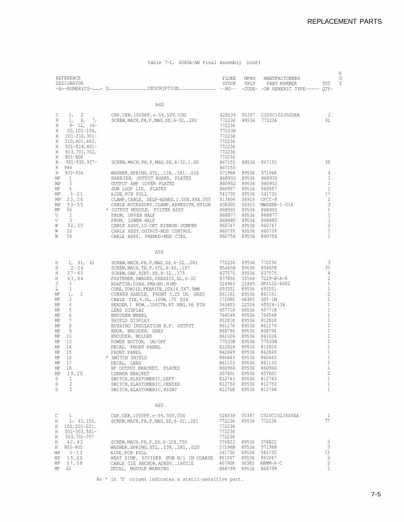
REPLACEMENT PARTS
7-5
Table 7-1. 6080A/AN Final Assembly (cont)
REFERENCEDESIGNATOR-A>-NUMERICS- >
C 1, 2H 1, 6, 7,H 9- 12, 16-H 20,101-104,H 201-216,301-H 310,401,402,H 501-514,601-H 613,701,702,H 801-808H 901-930,937-H 944H 933-936MP 1MP 3MP 4MP 5-21MP 23,24MP 53-55MP 56U 2U 3W 32,35W 33W 34
H 1, 41, 42H 2-36H 37-40H 43,44J 1L 1MP 1, 2MP 3MP 4MP 5MP 6MP 7MP 8MP 9MP 10MP 13MP 14MP 15MP 16MP 17MP 18MP 19,20S 1S 2S 3
C 1H 1- 41,101,H 102,201-221,H 301-303,501-H 503,701-707H 42,43H 903-905MP 1-13MP 19,20MP 57,58MP 62
S DESCRIPTION
A40
CAP,CER,1000PF,+-5%,50V,COGSCREW,MACH,PH,P,MAG,SS,6-32,.281
SCREW,MACH,PH,P,MAG,SS,6-32,1.00
WASHER,SPRING,STL,.138,.281,.020BARRIER, OUTPUT BOARD, PLATEDOUTPUT AMP COVER PLATEDSUM LOOP LID, PLATEDAIDE,PCB PULLCLAMP,CABLE, SELF-ADHES,1.00X.88X.055CABLE ACCESSORY,CLAMP,ADHESIVE,NYLON
* OUTPUT MODULE, FILTER ASSYPROM, UPPER HALFPROM, LOWER HALFCABLE ASSY,10-CKT RIBBON JUMPERCABLE ASSY,OUTPUT-MOD CONTROLCABLE ASSY. PREMOD-MOD CTRL
A50
SCREW,MACH,PH,P,MAG,SS,6-32,.281SCREW,MACH,TH,P,STL,4-40,.187SCREW,CAP,SCKT,SS,8-32,.375FASTENER,SWAGED,CHASSIS,AL,6-32ADAPTOR,COAX,SMA(M),N(M)CORE,TOROID,FERRITE,20X14.5X7.5MMCORNER HANDLE, FRONT 5.25 IN, GREYCABLE TIE,4.0L,.100W,.75 DIAHEADER,1 ROW,.100CTR,RT ANG,36 PINLENS DISPLAYENCODER WHEELSHIELD DISPLAYBUSHING INSULATION R.F. OUTPUTKNOB, ENCODER, GREYENCODER, MOLDEDPOWER BUTTON, ON/OFFDECAL, FRONT PANELFRONT PANEL
* SWITCH SHIELDDECAL, LENSRF OUTPUT BRACKET, PLATEDCORNER BRACKETSWITCH,ELASTOMERIC,LEFTSWITCH,ELASTOMERIC,CENTERSWITCH,ELASTOMERIC,RIGHT
A60
CAP,CER,1000PF,+-5%,50V,COGSCREW,MACH,PH,P,MAG,SS,6-32,.281
SCREW,MACH,PH,P,SS,6-32X.750WASHER,SPRING,STL,.138,.281,.020AIDE,PCB PULLHEAT SINK, DIVIDER (FOR N/l IN COARSECABLE TIE ANCHOR,ADHSV,.160TIEDECAL, MODULE WARNING
FLUKESTOCK
--NO--
528539772236772236772236772236772236772236772236772236867155867155571968868930860952860957541730513606838300868950868877868880860747860739860754
772236854658837575837856516963493551861161172080563403657718764548812818861174868794861026775338812826842849860643861133860960657601812743812750812768
528539772236772236772236772236376822571968541730861047407908868799
MFRSSPLY-CODE-
0539789536
89536
89536895368953689536895360691506915895368953689536895368953689536
89536895368953655566218458953689536063832252689536895368953689536895368953689536895368953689536895368953689536895368953689536
0539789536
895368953689536895360638389536
MANUFACTURERSPART NUMBER
-OR GENERIC TYPE-----
C320C102J5G5EA772236
867155
571968868930860952860957541730CFCC-8MWSSEB-1-01A868950868877868880860747860739860754
7722368546588375757229-B-A-6SF1132-6002493551861161SST-1M65524-136657718764548812818861174868794861026775338812826842849860643861133860960657601812743812750812768
C320C102J5G5EA772236
376822571968541730861047ABMM-A-C868799
TOTQTY-
281
38
41111723111211
33542112111111111111112111
177
2313221
N0T
An * in 'S' column indicates a static-sensitive part.
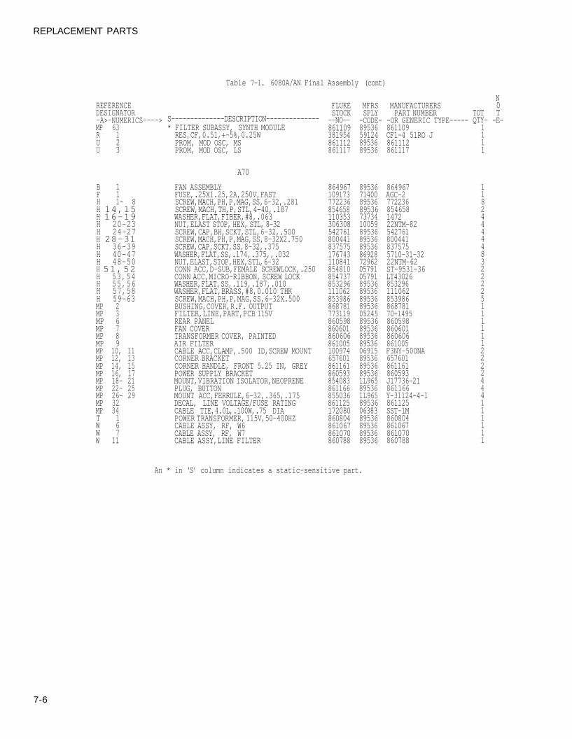
REPLACEMENT PARTS
7-6
Table 7-1. 6080A/AN Final Assemb1y (cont)
REFERENCEDESIGNATOR-A>-NUMERICS---->MP 63R 1U 2U 3
B 1F 1H 1- 8H 14,15H 16-19H 20-23H 24-27H 28-31H 36-39H 40-47H 48-50H 51,52H 53,54H 55,56H 57,58H 59-63MP 2MP 3MP 6MP 7MP 8MP 9MP 10, 11MP 12, 13MP 14, 15MP 16, 17MP 18- 21MP 22- 25MP 26- 29MP 32MP 34T 1W 6W 7W 11
S--------------DESCRIPTION--------------* FILTER SUBASSY, SYNTH MODULERES,CF,0.51,+-5%,0.25WPROM, MOD OSC, MSPROM, MOD OSC, LS
A70
FAN ASSEMBLYFUSE,.25X1.25,2A,250V,FASTSCREW,MACH,PH,P,MAG,SS,6-32,.281SCREW,MACH,TH,P,STL,4-40,.187WASHER,FLAT,FIBER,#8,.063NUT,ELAST STOP, HEX, STL, 8-32SCREW,CAP,BH,SCKT,STL,6-32,.500SCREW,MACH,PH,P,MAG,SS,8-32X2.750SCREW,CAP,SCKT,SS,8-32,.375WASHER,FLAT,SS,.174,.375,,.032NUT,ELAST,STOP,HEX,STL,6-32CONN ACC,D-SUB,FEMALE SCREWLOCK,.250CONN ACC,MICRO-RIBBON, SCREW LOCKWASHER,FLAT,SS,.119,.187,.010WASHER,FLAT,BRASS,#8,0.010 THKSCREW,MACH,PH,P,MAG,SS,6-32X.500BUSHING,COVER,R.F. OUTPUTFILTER,LINE,PART,PCB 115VREAR PANELFAN COVERTRANSFORMER COVER, PAINTEDAIR FILTERCABLE ACC,CLAMP,.500 ID,SCREW MOUNTCORNER BRACKETCORNER HANDLE, FRONT 5.25 IN, GREYPOWER SUPPLY BRACKETMOUNT,VIBRATION ISOLATOR,NEOPRENEPLUG, BUTTONMOUNT ACC,FERRULE,6-32,.365,.175DECAL, LINE VOLTAGE/FUSE RATINGCABLE TIE,4.0L,.100W,.75 DIAPOWER TRANSFORMER, 115V,50-400HZCABLE ASSY, RF, W6CABLE ASSY, RF, W7CABLE ASSY,LINE FILTER
FLUKESTOCK--NO--861109381954861112861117
864967109173772236854658110353306308542761800441837575176743110841854810854737853296111062853986868781773119860598860601860606861005100974657601861161860593854083861166855036861125172080860804861067861070860788
MFRSSPLY-CODE-89536591248953689536
89536714008953689536737341005989536895368953686928729620579105791895368953689536895360524589536895368953689536069158953689536895361L965895361L965895360638389536895368953689536
MANUFACTURERSPART NUMBER
-OR GENERIC TYPE-----861109CF1-4 51RO J861112861117
864967AGC-2772236854658147222NTM-825427618004418375755710-31-3222NTM-62ST-9531-36LT4302685329611106285398686878170-1495860598860601860606861005F3NY-500NA657601861161860593J17736-21861166Y-31124-4-1861125SST-1M860804861067861070860788
TOTQTY-
1111
11824444483222251111112222444111111
N0T-E-
An * in 'S' column indicates a static-sensitive part.
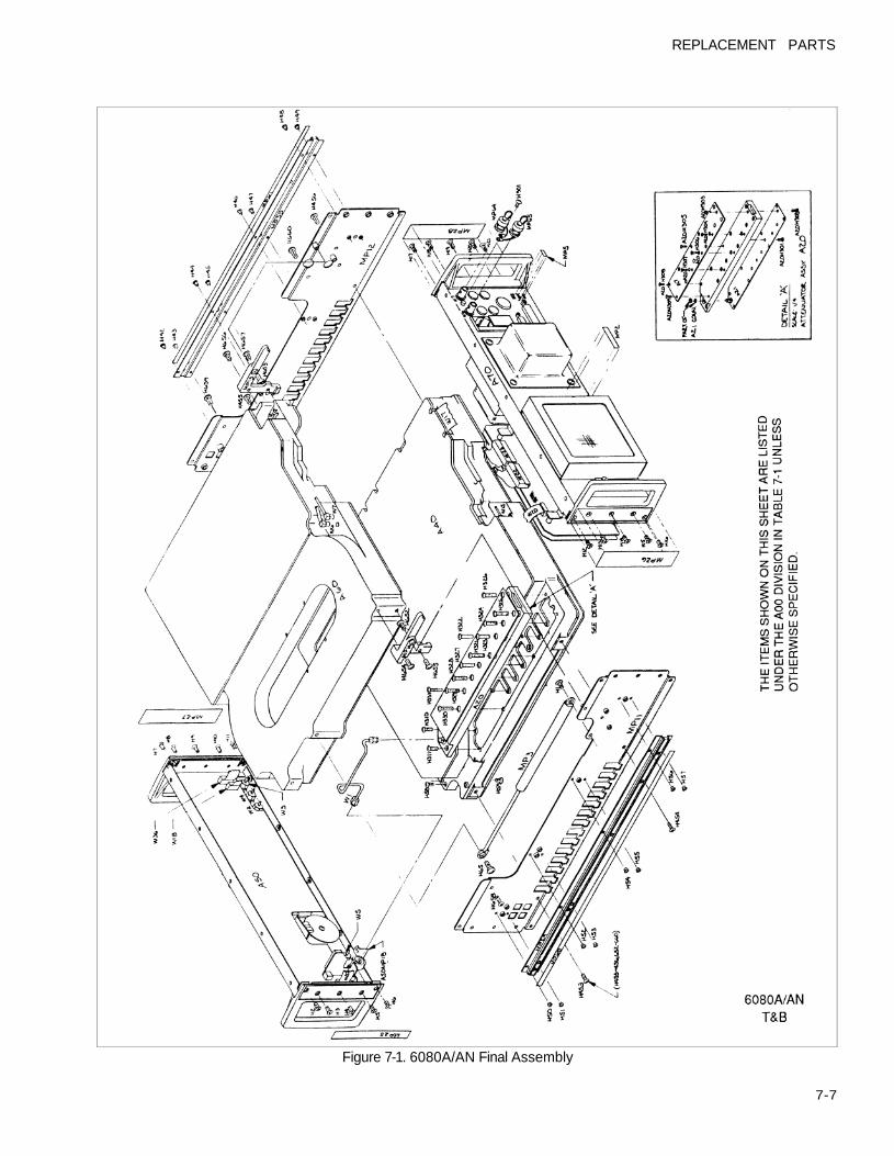
REPLACEMENT PARTS
Figure 7-1. 6080A/AN Final Assembly
7-7
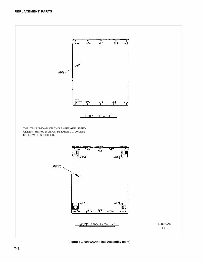
REPLACEMENT PARTS
Figure 7-1. 6080A/AN Final Assembly (cont)
7-8
THE ITEMS SHOWN ON THIS SHEET ARE LISTEDUNDER THE A00 DIVISION IN TABLE 7-1 UNLESSOTHERWISE SPECIFIED.
6080A/ANT&B
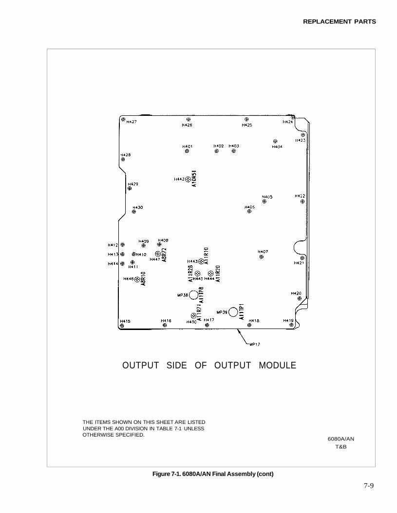
REPLACEMENT PARTS
7-9
Figure 7-1. 6080A/AN Final Assembly (cont)
OUTPUT SIDE OF OUTPUT MODULE
THE ITEMS SHOWN ON THIS SHEET ARE LISTEDUNDER THE A00 DIVISION IN TABLE 7-1 UNLESSOTHERWISE SPECIFIED.
6080A/AN
T&B
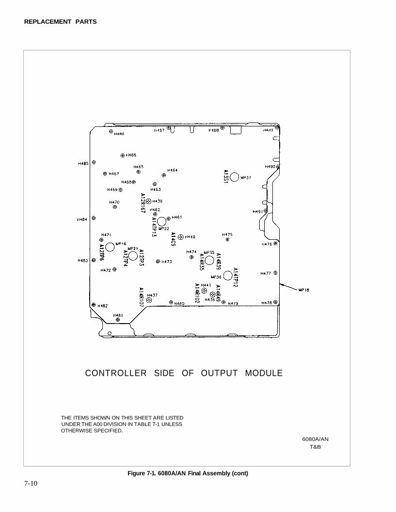
REPLACEMENT PARTS
Figure 7-1. 6080A/AN Final Assembly (cont)
7-10
CONTROLLER SIDE OF OUTPUT MODULE
THE ITEMS SHOWN ON THIS SHEET ARE LISTEDUNDER THE A00 DIVISION IN TABLE 7-1 UNLESSOTHERWISE SPECIFIED.
6080A/AN
T&B
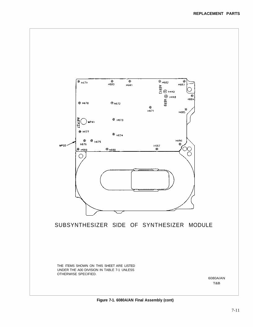
REPLACEMENT PARTS
7-11
Figure 7-1. 6080A/AN Final Assembly (cont)
SUBSYNTHESIZER SIDE OF SYNTHESIZER MODULE
THE ITEMS SHOWN ON THIS SHEET ARE LISTEDUNDER THE A00 DIVISION IN TABLE 7-1 UNLESSOTHERWISE SPECIFIED.
6080A/AN
T&B
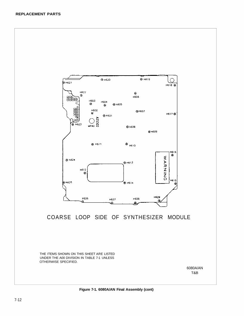
REPLACEMENT PARTS
Figure 7-1. 6080A/AN Final Assembly (cont)
7-12
COARSE LOOP SIDE OF SYNTHESIZER MODULE
THE ITEMS SHOWN ON THIS SHEET ARE LISTEDUNDER THE A00 DIVISION IN TABLE 7-1 UNLESSOTHERWISE SPECIFIED.
6080A/ANT&B
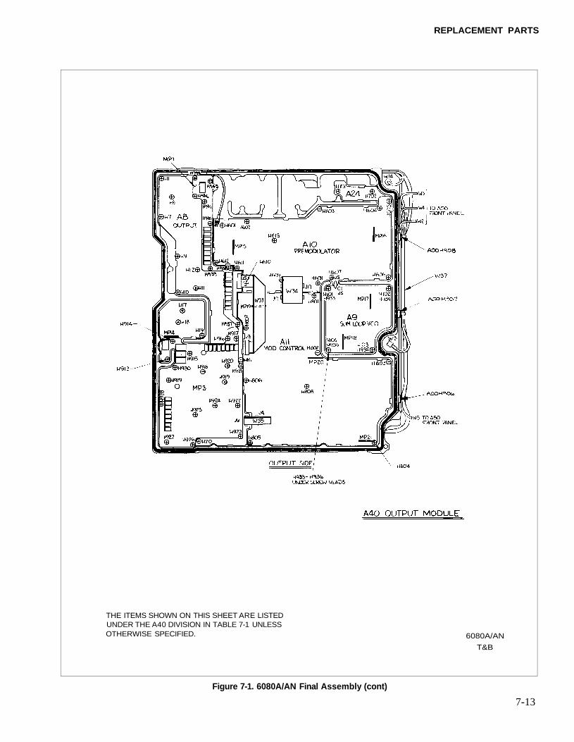
REPLACEMENT PARTS
Figure 7-1. 6080A/AN Final Assembly (cont)
7-13
THE ITEMS SHOWN ON THIS SHEET ARE LISTEDUNDER THE A40 DIVISION IN TABLE 7-1 UNLESSOTHERWISE SPECIFIED. 6080A/AN
T&B
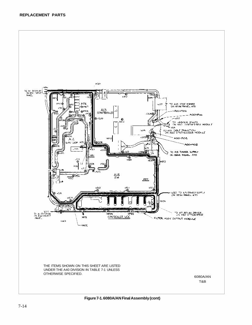
REPLACEMENT PARTS
Figure 7-1. 6080A/AN Final Assembly (cont)
7-14
THE ITEMS SHOWN ON THIS SHEET ARE LISTEDUNDER THE A40 DIVISION IN TABLE 7-1 UNLESSOTHERWISE SPECIFIED.
6080A/AN
T&B
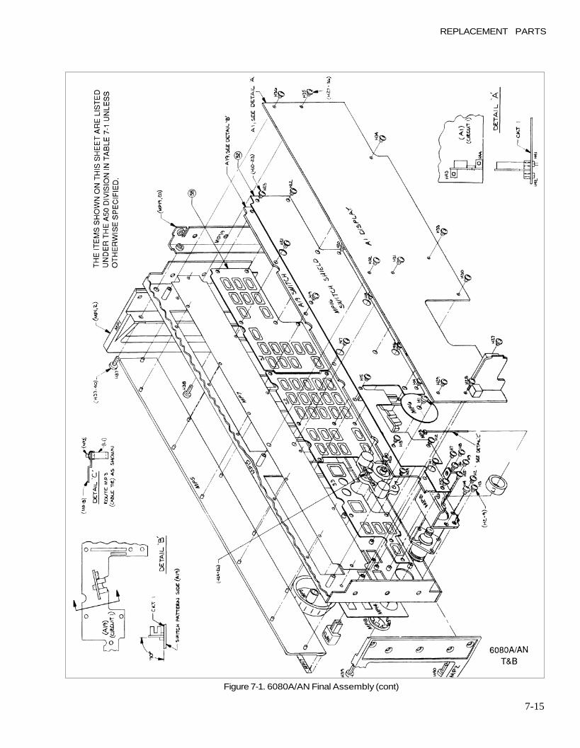
REPLACEMENT PARTS
Figure 7-1. 6080A/AN Final Assembly (cont)
7-15
6080A/ANT&B
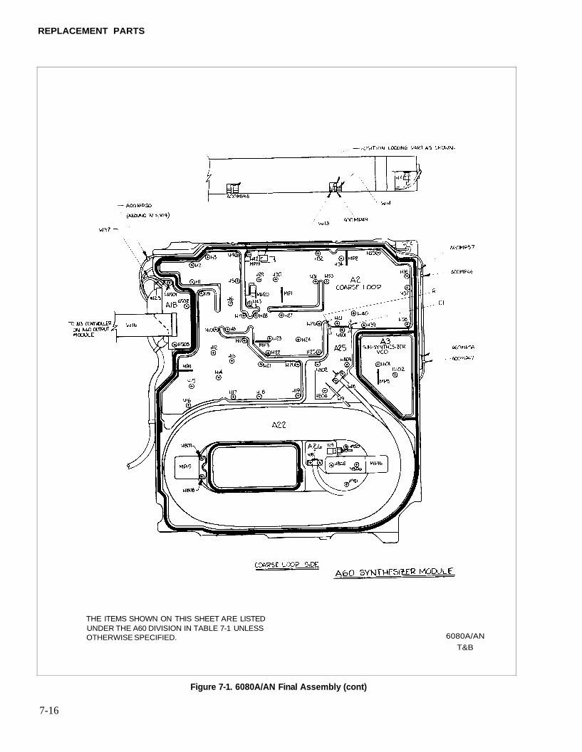
REPLACEMENT PARTS
Figure 7-1. 6080A/AN Final Assembly (cont)
7-16
THE ITEMS SHOWN ON THIS SHEET ARE LISTEDUNDER THE A60 DIVISION IN TABLE 7-1 UNLESSOTHERWISE SPECIFIED. 6080A/AN
T&B
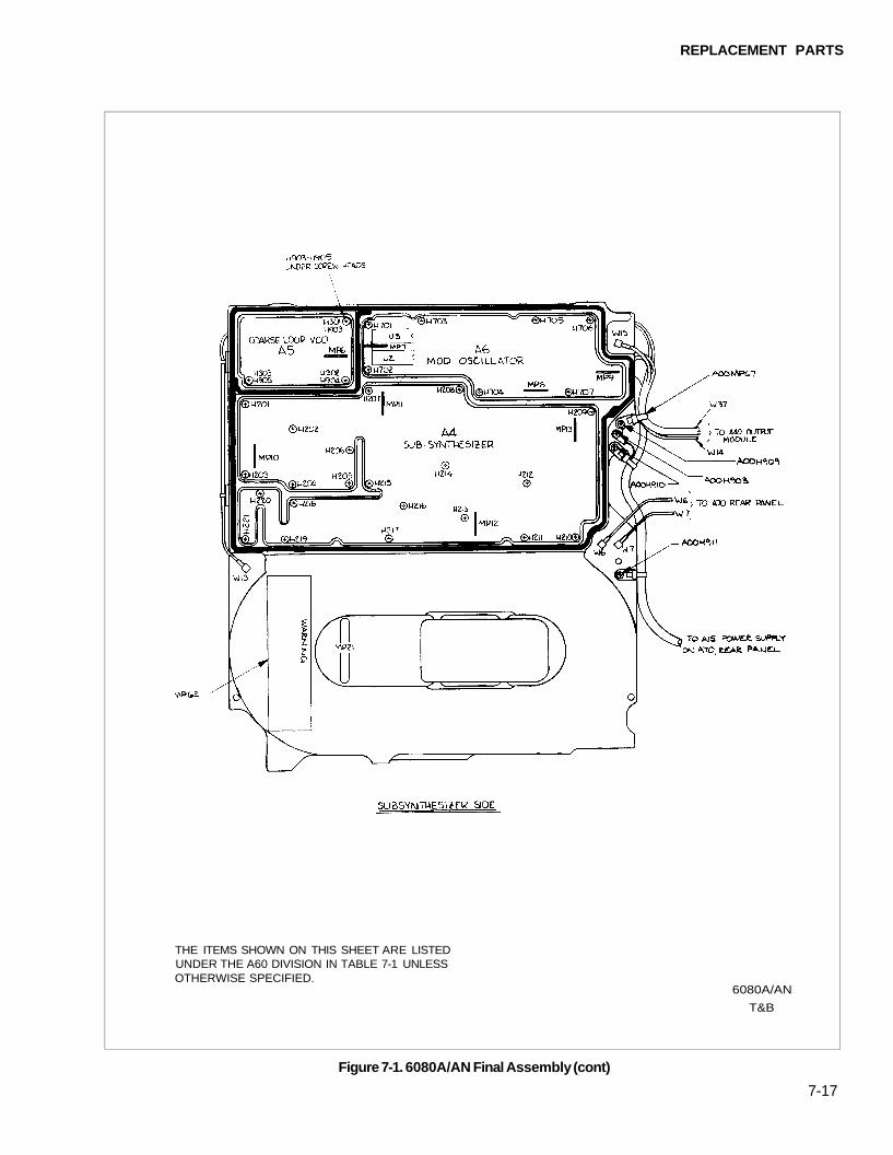
REPLACEMENT PARTS
7-17
Figure 7-1. 6080A/AN Final Assembly (cont)
THE ITEMS SHOWN ON THIS SHEET ARE LISTEDUNDER THE A60 DIVISION IN TABLE 7-1 UNLESSOTHERWISE SPECIFIED.
6080A/AN
T&B
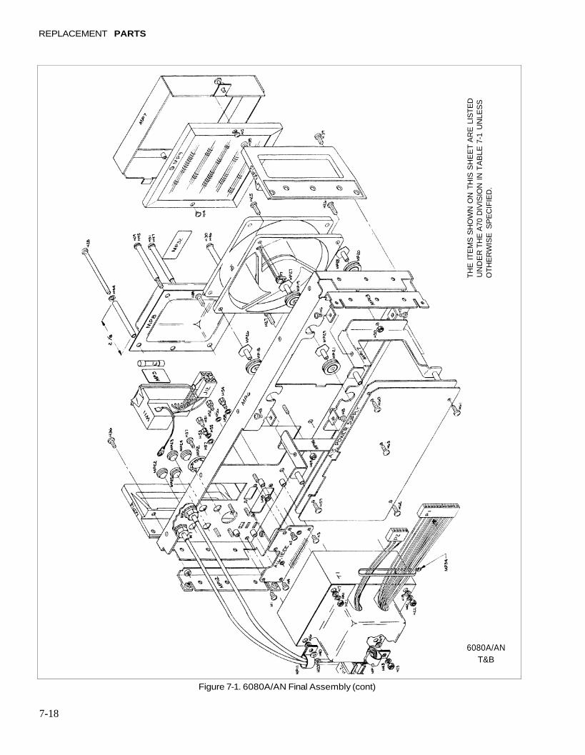
REPLACEMENT PARTS
Figure 7-1. 6080A/AN Final Assembly (cont)
7-18
TH
E I
TE
MS
SH
OW
N O
N T
HIS
SH
EE
T A
RE
LIS
TE
DU
ND
ER
TH
E A
70 D
IVIS
ION
IN
TA
BLE
7-1
UN
LES
SO
TH
ER
WIS
E S
PE
CIF
IED
.
6080A/ANT&B
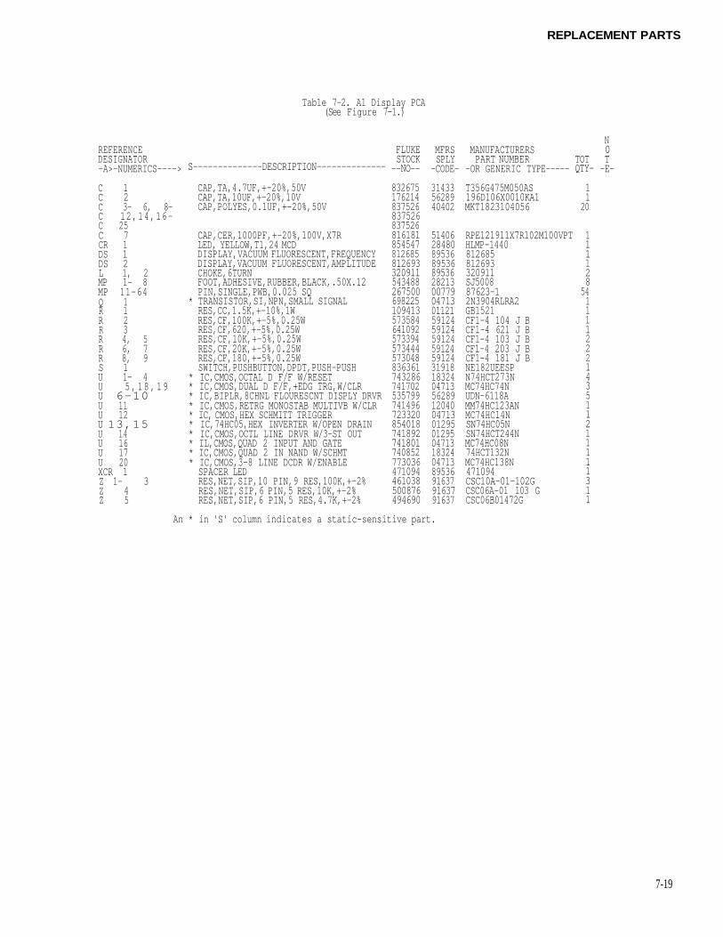
REPLACEMENT PARTS
7-19
Tab1e 7-2. A1 Display PCA(See Figure 7-1.)
REFERENCEDESIGNATOR-A>-NUMERICS---->
C 1C 2C 3- 6, 8-C 12,14,16-C 25C 7CR 1DS 1DS 2L 1, 2MP 1- 8MP 11-64Q 1R 1R 2R 3R 4, 5R 6, 7R 8, 9S 1U 1- 4U 5,18,19U 6-10U 11U 12U 13,15U 14U 16U 17U 20XCR 1Z 1- 3Z 4Z 5
S--------------DESCRIPTION--------------
CAP,TA,4.7UF,+-20%,50VCAP,TA,10UF,+-20%,10VCAP,POLYES,0.1UF,+-20%,50V
CAP,CER,1000PF,+-20%,100V,X7RLED, YELLOW,T1,24 MCDDISPLAY,VACUUM FLUORESCENT,FREQUENCYDISPLAY,VACUUM FLUORESCENT,AMPLITUDECHOKE,6TURNFOOT,ADHESIVE,RUBBER,BLACK,.50X.12PIN,SINGLE,PWB,0.025 SQ
* TRANSISTOR,SI,NPN,SMALL SIGNALRES,CC,1.5K,+-10%,1WRES,CF,100K,+-5%,0.25WRES,CF,620,+-5%,0.25WRES,CF,10K,+-5%,0.25WRES,CF,20K,+-5%,0.25WRES,CF,180,+-5%,0.25WSWITCH,PUSHBUTTON,DPDT,PUSH-PUSH
* IC,CMOS,OCTAL D F/F W/RESET* IC,CMOS,DUAL D F/F,+EDG TRG,W/CLR* IC,BIPLR,8CHNL FLOURESCNT DISPLY DRVR* IC,CMOS,RETRG MONOSTAB MULTIVB W/CLR* IC, CMOS,HEX SCHMITT TRIGGER* IC,74HC05,HEX INVERTER W/OPEN DRAIN* IC,CMOS,OCTL LINE DRVR W/3-ST OUT* IL,CMOS,QUAD 2 INPUT AND GATE* IC,CMOS,QUAD 2 IN NAND W/SCHMT* IC,CMOS,3-8 LINE DCDR W/ENABLESPACER LEDRES,NET,SIP,10 PIN,9 RES,100K,+-2%RES,NET,SIP,6 PIN,5 RES,10K,+-2%RES,NET,SIP,6 PIN,5 RES,4.7K,+-2%
FLUKESTOCK--NO--
832675176214837526837526837526816181854547812685812693320911543488267500698225109413573584641092573394573444573048836361743286741702535799741496723320854018741892741801740852773036471094461038500876494690
MFRSSPLY
-CODE-
314335628940402
5140628480895368953689536282130077904713011215912459124591245912459124319181832404713562891204004713012950129504713183240471389536916379163791637
MANUFACTURERSPART NUMBER
-OR GENERIC TYPE-----
T356G475M050AS196D106X0010KA1MKT1823104056
RPE121911X7R102M100VPTHLMP-1440812685812693320911SJ500887623-12N3904RLRA2GB1521CF1-4 104 J BCF1-4 621 J BCF1-4 103 J BCF1-4 203 J BCF1-4 181 J BNE182UEESPN74HCT273NMC74HC74NUDN-6118AMM74HC123ANMC74HC14NSN74HC05NSN74HCT244NMC74HC08N74HCT132NMC74HC138N471094CSC10A-01-102GCSC06A-01 103 GCSC06B01472G
TOTQTY-
11
20
111128541111222143511211111311
N0T-E-
An * in 'S' column indicates a static-sensitive part.
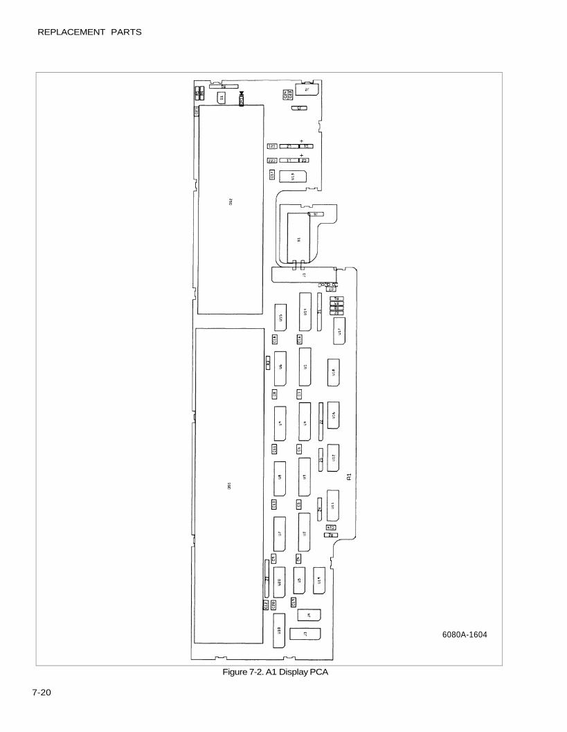
REPLACEMENT PARTS
Figure 7-2. A1 Display PCA
7-20
6080A-1604
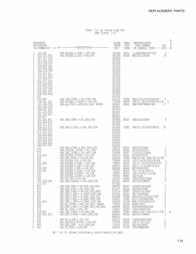
REPLACEMENT PARTS
7-21
Table 7-3. A2 Coarse Loop PCA(See Figure 7-3.)
REFERENCEDESIGNATOR-A>-NUMERICS---->
C 101,218C 102,107,206,C 207,217,219,C 221,222,226,C 227,230,236-C 238,245,249,C 253-263,265,C 266,270,305-C 312,410,411,C 415,417,424,C 427,429,507-C 512,517,520-C 522,526-528,C 531-536,539,C 540,543,548,C 619,630,631,C 638,639,642,C 651C 103,605C 104,231,232C 105,106,239,C 240,242,243,C 246,247,250,C 251,274,506,C 541,542,601,C 603,613C 201,302,401,C 402,404,413,C 414,611,614C 204,210,273,C 406-409,501,C 513,516,518,C 544,602,606,C 609,610,612,C 615,620,624,C 625,640,641,C 646,647,652C 211C 212C 213C 214,216C 215C 220C 223,224C 225C 228,229C 233,267C 234C 235C 264C 301,303,304,C 313,314C 403C 405C 412C 421C 422C 423C 425,426C 428C 430C 514C 519,550C 523-525,537,C 538C 529C 530C 545C 546
S--------------DESCRIPTION--------------
CAP,POLYES,0.47UF,+-10%,50VCAP,POLYES,0.1UF,+-20%,50V
CAP,CER,220PF,+-2%,100V,C0GCAP,POLYES,0.022UF,+-10%,50VCAP,AL,47UF,+-20%,50V,SOLV PROOF
CAP,CER,100PF,+-2%,100V,C0G
CAP,CER,0.01UF,+-20%, 50V, X7R
CAP,CER,470PF,+-20%,100V,X7RCAP,POLYPR, 2200PF,+-5%, 100VCAP,CER,150PF,+-2%,100V,C0GCAP,POLYPR,4700PF,+-5%,63VCAP,CER,390PF,+-2%,50V,C0GCAP,POLYES,1UF,+-10%,50VCAP,POLYES,0.22UF,+-10%,50VCAP,POLYES,0.1UF,+-10%,50VCAP,POLYES,2.2UF,+-10%,50VCAP,POLYES,0.01UF,+-10%,50VCAP,POLYES,4700PF,+-5%,50VCAP,POLYES,2200PF,+-10%,50VCAP,TA,1UF,+-10%,35VCAP,CER,1000PF,+-20%,100V,X7R
CAP,CER,10PF,+-5%,50V,C0G,0805CAP,CER,27PF,+-2%,100V,C0GCAP,CER,100PF,+-5%,50V,C0G,0805CAP,CER,1.5PF,+-0.25PF,100V,C0KCAP,CER,2.2PF,+-0.25PF,100V,C0JCAP,CER,1.8PF,+-0.25PF,100V,C0KCAP,CER,l.2PF,+-0.25PF,100V,C0KCAP,AL,470UF,+-20%,16V,SOLV PROOFCAP,CER,3.9PF,+-0.25PF,50V,C0G,0805CAP,TA,10UF,+-20%,15VCAP,CER,270PF,+-5%,50V,C0GCAP,CER,4700PF,+-20%,100V,X7R
CAP,TA,2.2UF,+-10%,15VCAP,POLYES,0.047UF,+-10%,50VCAP,CER,12PF, +-2%,100V,C0GCAP,TA,39UF,+-20%,20V
FLUKESTOCK
--NO--
697409837526837526837526837526837526837526837526837526837526837526837526837526837526837526837526837526837526812131715268822403822403822403822403822403822403837609837609837609816249816249816249816249816249816249816249816249358275854505512988854513820530733089706028649913854500715037739987780536161919837542837542494781812107514133812164812099512897543256772855493874193623658898866426866426364216714709715169358234
MFRSSPLY-CODE-
8441140402
729826093562643
04222
72982
0422240402053974040272982609356093560935404026093560935968815628904222
053970422205397042227298272982514066105804222562897298204222
56289609350422231433
MANUFACTURERSPART NUMBER
-OR GENERIC TYPE-----
J1320R47MF10PCT50VMKT1823104056
RPE121911COG221G100V185-2/.022/K/0050/R/C/KME50VB47RM6X11RP
SR201A101GATR
RPE121-911X7R103M50V
SR151C471KATKP1830222014C315C151J1G5EAKP1830472064RPE122-901-COG-391-G-5185/1.00/K/0050/R/G/B185-2/.22/K/0050/R/C/B185-0 .1-K-0050-R-A-BMKT1826225055185-.01-K-0050-R168-2/4700/J/50/AAIR67222K196D105X0035HA1SR151C102MATR
CC805C100J5GATSR291A270GAACO805C101J5GATSR171A1R5CAARPE121911COJ2R2C100V8101-100COKO189BRPE110C0G1R2G100VECEA1CU47108055A3R9CAT065B195D106X0015A1RPE122-901-COG-271-J-5SR151C472MATR
196D225X0015HA1168-2/.047/K/ASR211A126GATT361396M020AS
TOTQTY-
275
2B 317
9
26
1112
0V121221115
1111112111
0V5
1111
N0T-E-
2
An * in 'S' column indicates a static-sensitive part.
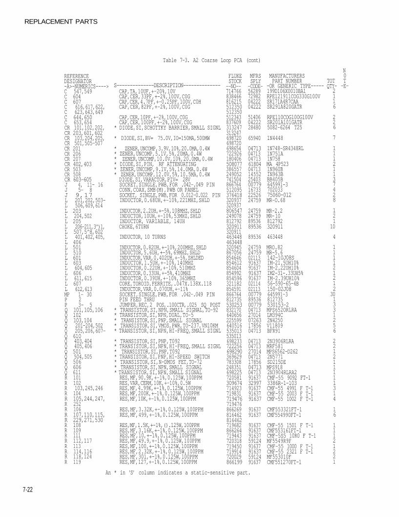
Table 7-3. A2 Coarse Loop PCA (cont)
REFERENCEDESIGNATOR-A>-NUMERICS---->C 547,549C 604C 607C 616,617,622,C 623,643,649C 644,650C 653,654CR 101,102,202,CR 203,601,602CR 103,204,205,CR 501,505-507CR 201CR 206CR 207CR 402,403CR 503CR 508CR 603-605J 4, 11- 16J 5- 8J 9,17L 201,202,503-L 506,609,614L 203L 204,502L 205L 206-211,3̂ )1,L 507,5^8,602L 401,402,405,L 406L 501L 510L 601L 603L 604,605L 606L 611,615L 607L 612,613MP 1- 30P 2P 3- 5Q 101,105,106Q 102Q 103,104Q 201-204,502Q 205,206,607-Q 610Q 403,404Q 405,406Q 501Q 504,505Q 506Q 606Q 611R 101R 102R 103,245,246R 104R 105,244,247,R 252R 106R 107,110,115,R 229,271,530R 108R 109R 111R 112,117R 113R 114,116R 118,124R 119
S--------------DESCRIPTION--------------CAP,TA,10UF,+-20%,10VCAP,CER,33PF,+-2%,100V,C0GCAP,CER,4.7PF,+-0.25PF,100V,C0HCAP,CER,82PF,+-2%,100V,C0G
CAP,CER,10PF,+-2%,100V,C0GCAP,CER,100PF,+-2%,100V,C0G
* DIODE,SI,SCHOTTKY BARRIER,SMALL SIGNL
* DIODE,SI,BV= 75.0V,IO=150MA,500MW
* ZENER,UNCOMP,3.9V,10%,20.0MA,0.4W* ZENER,UNCOMP,5.1V,5%,20MA,0.4W* ZENER,UNCOMP,10.0V,10%,20.0MA,0.4W* DIODE,SI,PIN, RF ATTENUATING* ZENER,UNCOMP,9.1V,5%,14.0MA,0.4W* ZENER,UNCOMP,12.0V,5%,10.5MA,0.4WDIODE,SI,VARACTOR,PIV= 28VSOCKET,SINGLE,PWB,FOR .042-.049 PINCONN,COAX,SMB(M),PWB OR PANELSOCKET, SINGLE,PWB,FOR 0.012-0.022 PININDUCTOR,0.68UH,+-10%,221MHZ,SHLD
INDUCTOR,2.2UH,+-5%,108MHZ,SHLDINDUCTOR,10UH,+-10%,53MHZ,SHLDINDUCTOR, VARIABLE, 14UHCHOKE,6TURN
INDUCTOR, 10 TURNS
INDUCTOR,0.82UH,+-10%,200MHZ,SHLDINDUCTOR,5.6UH,+-5%,69MHZ,SHLDINDUCTOR,VAR,0.402UH,+-5%,SHLDEDINDUCTOR,1.5UH,+-10%,140MHZINDUCTOR,0.22UH,+-10%,510MHZINDUCTOR,0.33UH,+-5%,410MHZINDUCTOR,0.39UH,+-10%,365MHZCORE,TOROID,FERRITE,.047X.138X.118INDUCTOR,VAR,0.070UH,+-11%SOCKET,SINGLE,PWB,FOR .042-.049 PINPIN FEED THRUJUMPER,REC,2 POS,.100CTR,.025 SQ POST
* TRANSISTOR,SI,NPN,SMALL SIGNAL,TO-92* TRANSISTOR,SI,NPN,DUAL,TO-5* TRANSISTOR,SI,PNP,SMALL SIGNAL* TRANSISTOR,SI,VMOS,PWR,TO-237,VN10KM* TRANSISTOR,SI,NPN,HI-FREQ,SMALL SIGNL
* TRANSISTOR,SI,PNP,T092* TRANSISTOR,SI,NPN,HI-FREQ,SMALL SIGNL* TRANSISTOR,SI,PNP,T092* TRANSISTOR,SI,PNP,HI-SPEED SWITCH* TRANSISTOR,SI,N-DMOS FET,TO-72* TRANSISTOR,SI,NPN,SMALL SIGNAL* TRANSISTOR,SI,NPN,SMALL SIGNALRES,MF,90.9K,+-1%,0.125W,100PPMRES,VAR,CERM,10K,+-10%,0.5WRES,MF,4.99K,+-1%,0.125W,100PPMRES,MF,200K,+-1%,0.125W,100PPMRES,MF,10K,+-1%,0.125W,100PPM
RES,MF,3.32K,+-1%,0.125W,100PPMRES,MF,499,+-1%,0.125W,100PPM
RES,MF,1.5K,+-1%,().125W,100PPMRES,MF,3.16K,+-1%,0.125W,100PPMRES,MF,10,+-1%,0.125W,100PPMRES,MF,49.9,+-1%,0.125W,100PPMRES,MF,100,+-1%,0.125W,100PPMRES,MF,2.32K,+-1%,0.125W,100PPMRES,MF,301,+-1%,0.125W,100PPMRES,MF,127,+-1%,0.125W,100PPM
FLUKESTOCK--NO--714766838466816215512350512350512343837609313247313247698720698720698654722926180406508077386557249052741504866764512095376418320937320937806547249078812792320911320911463448463448320945867056854646854612854604854992854596321182854591866764812735530253832170640656225599640516535013535013698233722256698290369629783308248351698225720581309674714923719831719476719476866269816462816462719682866264719443720318719450719914720029866199
MFRSSPLY-CODE-56289729820422204222
514060422228480
65940
0471304713047136180404713145522540300779167332252624759
24759247598953689536
89536
2475924759021139163791637916379163702114021130077989536007790471327014072631785604713
047130471327014047131785604713047139163732997916379163791637
9163791637
9163791637916375912491637916375912491637
MANUFACTURERSPART NUMBER
-OR GENERIC TYPE-----199D106X0010BA1RPE121911COG330G100VSR171A4R7CAASR291A820GATR
RPE110COG100G100VSR201A101GATR5082-6264 T25
1N4448
1N748-SR4348RL1N751A1N758MA 4P5231N960BIN963BBB405B645991-370203375060-012MR-O.68
MR-2.2MR- 10812792320911
463448
MRO.82MR-5.6142-10J08SIM-21.5UH10%IM-2.22UH10%IM2-31-.33UH5%IM-2.39UH10%56-590-65-4B150-02J08645991-3812735530153-2MPS652ORLRALM394C2N4250V11809BFR91
2N3906RLRAMRF581MPS6562-D2622N5771SD215DEMPS9182N3904RLRA2CMF-55 9092 FT-13386R-1-103CMF-55 4991 F T-1CMF-55 2003 F T-1CMF-55 1002 F T-1
CMF553321FT-1CMF554990FT-1
CMF-55 1501 F T-1CMF553161FT-1CMF-5S5 10R0 F T-1MF5549R9FCMF-55 1000 F T-1CMF-55 2321 F T-1MF553010FCMF551270FT-1
TOTQTY-2116
226
7
11121137428
12110
4
111121212301331256
221211111314
16
11121221
N0T-E-
An * in 'S' column indicates a static-sensitive part.
REPLACEMENT PARTS
7-22
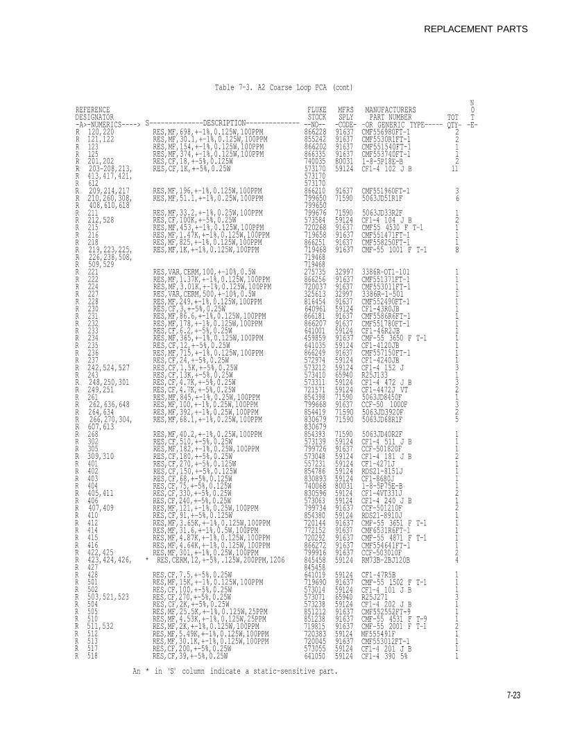
REPLACEMENT PARTS
7-23
Table 7-3. A2 Coarse Loop PCA (cont)
REFERENCEDESIGNATOR-A>-NUMERICS---->R 120,220R 121,122R 123R 125R 201,202R 203-208,213,R 413,417,421,R 612R 209,214,217R 210,260,308,R 408,610,618R 211R 212,528R 215R 216R 218R 219,223,225,R 226,238,508,R 509,529R 221R 222R 224R 227R 228R 230R 231R 232R 233R 234R 235R 236R 237R 242,524,527R 243R 248,250,301R 249,251R 261R 262,636,648R 264,634R 266,270,304,R 607,613R 268R 302R 305R 309,310R 401R 402R 403R 404R 405,411R 406R 407,409R 410R 412R 414R 415R 416R 422,425R 423,424,426,R 427R 428R 501R 502R 503,521,523R 504R 505R 510R 511,532R 512R 513R 517R 518
S--------------DESCRIPTION--------------RES,MF,698,+-1%,0.125W,100PPMRES,MF,30.1,+-1%,0.125W,100PPMRES,MF,154,+-1%,0.125W,100PPMRES,MF,374,+-1%,0.125W,100PPMRES,CF,18,+-5%,0.125WRES,CF,1K,+-5%,0.25W
RES,MF,196,+-1%,0.125W,100PPMRES,MF,51.1,+-1%,0.25W,100PPM
RES,MF,33.2,+-1%,0.25W,100PPMRES,CF,100K,+-5%,0.25WRES,MF,453,+-1%,0.125W,100PPMRES,MF,1.47K,+-1%,0.125W,100PPMRES,MF,825,+-1%,0.125W,100PPMRES,MF,1K,+-1%,0.125W,100PPM
RES,VAR,CERM,100,+-10%,0.5WRES,MF,1.37K,+-1%,0.125W,100PPMRES,MF,3.01K,+-1%,0.125W,100PPMRES,VAR,CERM,500,+-10%,0.5WRES,MF,249,+-1%,0.125W,100PPMRES,CF,3,+-5%,0.25WRES,MF,86.6,+-1%,0.125W,100PPMRES,MF,178,+-1%,0.125W,100PPMRES,CF,6.2,+-5%,0.25WRES,MF,365,+-1%,0.125W,100PPMRES,CF,12,+-5%,0.25WRES,MF,715,+-1%,0.125W,100PPMRES,CF,24,+-5%,0.25WRES,CF,1.5K,+-5%,0.25WRES,CF,13K,+-5%,0.25WRES,CF,4.7K,+-5%,0.25WRES,CF,4.7K,+-5%,0.25WRES,MF,845,+-1%,0.25W,100PPMRES,MF,100,+-1%,0.25W,100PPMRES,MF,392,+-1%,0.25W,100PPMRES,MF,68.1,+-1%,0.25W,100PPM
RES,MF,40.2,+-1%,0.25W,100PPMRES,CF,510,+-5%,0.25WRES,MF,182,+-1%,0.25W,100PPMRES,CF,180,+-5%,0.25WRES,CF,270,+-5%,0.125WRES,CF,150,+-5%,0.125WRES,CF,68,+-5%,0.125WRES,CF,75,+-5%,0.125WRES,CF,330,+-5%,0.25WRES,CF,240,+-5%,0.25WRES,MF,121,+-1%,0.25W,100PPMRES,CF,91,+-5%,0.125WRES,MF,3.65K,+-1%,0.125W,100PPMRES,MF,31.6,+-1%,0.5W,100PPMRES,MF,4.87K,+-1%,0.125W,100PPMRES,MF,4.64K,+-1%,0.125W,100PPMRES,MF,301,+-1%,0.25W,100PPM
* RES,CERM,12,+-5%,.125W,200PPM,1206
RES,CF,7.5,+-5%,0.25WRES,MF,15K,+-1%,0.125W,100PPMRES,CF,100,+-5%,0.25WRES,CF,270,+-5%,0.25WRES,CF,2K,+-5%,0.25WRES,MF,25.5K,+-1%,0.125W,25PPMRES,MF,4.53K,+-1%,0.125W,25PPMRES,MF,2K,+-1%,0.125W,100PPMRES,MF,5.49K,+-1%,0.125W,100PPMRES,MF,30.1K,+-1%,0.125W,100PPMRES,CF,200,+-5%,0.25WRES,CF,39,+-5%,0.25W
FLUKESTOCK
--NO--866228855242866202866335740035573170573170573170866210799650799650799676573584720268719658866251719468719468719468275735866256720037325613816454640961866181866207641001459859641035866249572974573212573410573311721571854398799668854419830679830679854393573139799726573048557231854786830893740068830596573063799734854380720144772152720292866272799916845458845458641019719690573014573071573238851212851238719815720383720045573055641050
MFRSSPLY
-CODE-916379163791637916378003159124
9163771590
715905912491637916379163791637
329979163791637329979163759124916379163759124916375912491637591245912465940591245912471590916377159071590
715905912491637591245912459124591248003159124591249163759124916379163791637916379163759124
591249163759124659405912491637916379163759124916375912459124
MANUFACTURERSPART NUMBER
-OR GENERIC TYPE-----CMF556980FT-1CMF5530R1FT-1CMF551540FT-1CMF553740FT-11-8-5P18E-BCF1-4 102 J B
CMF551960FT-15063JD51R1F
5063JD33R2FCF1-4 104 J BCMF55 4530 F T-1CMF551471FT-1CMF558250FT-1CMF-55 1001 F T-1
3386R-OT1-101CMF551371FT-1CMF553011FT-13386R-1-501CMF552490FT-1CF1-43R0JBCMF5586R6FT-1CMF551780FT-1CF1-46R2JBCMF-55 3650 F T-1CF1-4120JBCMF557150FT-1CF1-4240JBCF1-4 152 JR25J133CF1-4 472 J BCF1-4472J VT5063JD8450FCCF-50 1000F5063JD3920F5063JD68R1F
5063JD40R2FCF1-4 511 J BCCF-501820FCF1-4 181 J BCF1-4271JRDS21-8151JCF1-8680J1-8-5P75E-BCF1-4VT331JCF1-4 240 J BCCF-501210FRDS21-8910JCMF-55 3651 F T-1CMF6531R6FT-1CMF-55 4871 F T-1CMF554641FT-1CCF-503010FRM73B-2BJ120B
CF1-47R5BCMF-55 1502 F T-1CF1-4 101 J BR25J271CF1-4 202 J BCMF552552FT-9CMF-55 4531 F T-9CMF-55 2001 F T-1MF555491FCMF553012FT-1CF1-4 201 J BCF1-4 390 5%
TOTQTY-
22112
11
36
121118
111111111111131321325
111211112121111124
111311121111
N0T-E-
An * in 'S' column indicate a static-sensitive part.
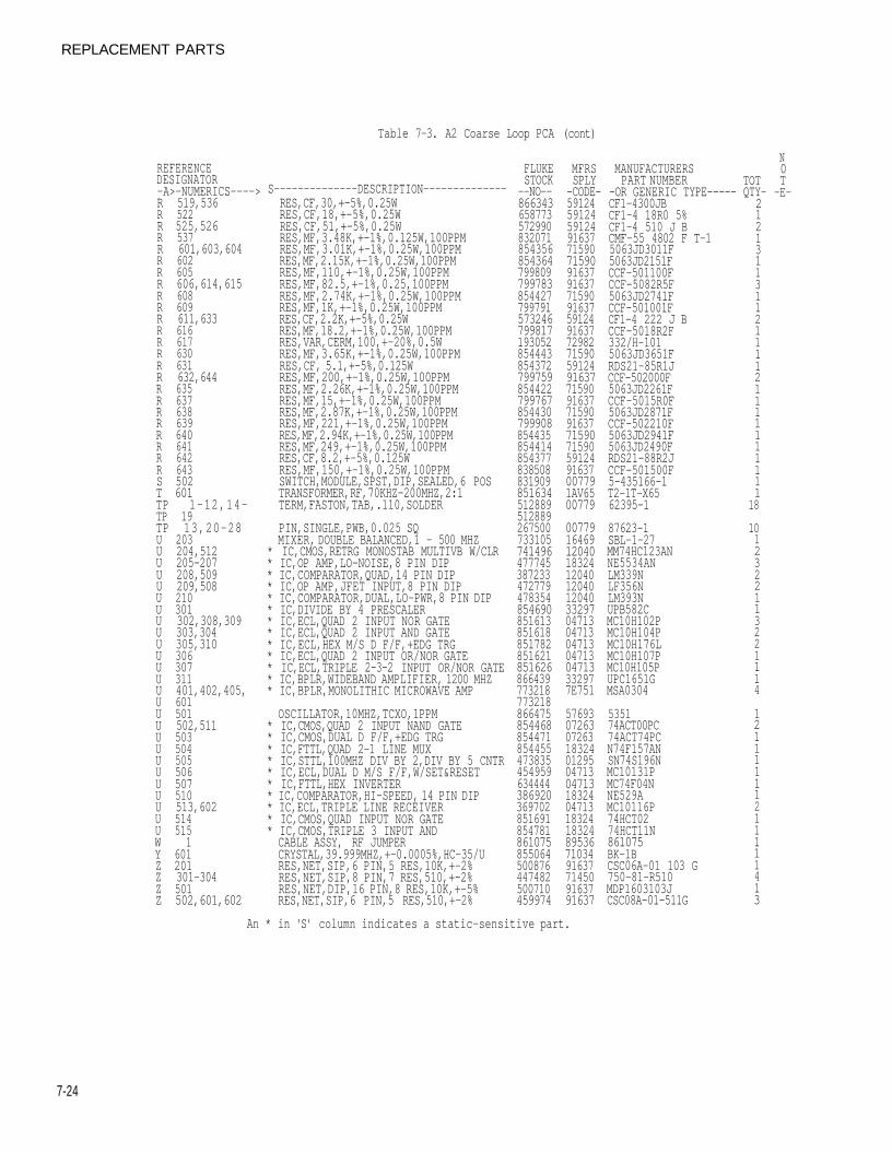
REPLACEMENT PARTS
7-24
Table 7-3. A2 Coarse Loop PCA (cont)
REFERENCEDESIGNATOR-A>-NUMERICS---->R 519,536R 522R 525,526R 537R 601,603,604R 602R 605R 606,614,615R 608R 609R 611,633R 616R 617R 630R 631R 632,644R 635R 637R 638R 639R 640R 641R 642R 643S 502T 601TP 1-12,14-TP 19TP 13,20-28U 203U 204,512U 205-207U 208,509U 209,508U 210U 301U 302,308,309U 303,304U 305,310U 306U 307U 311U 401,402,405,U 601U 501U 502,511U 503U 504U 505U 506U 507U 510U 513,602U 514U 515W 1Y 601Z 201Z 301-304Z 501Z 502,601,602
S--------------DESCRIPTION--------------RES,CF,30,+-5%,0.25WRES,CF,18,+-5%,0.25WRES,CF,51,+-5%,0.25WRES,MF,3.48K,+-1%,0.125W,100PPMRES,MF,3.01K,+-1%,0.25W,100PPMRES,MF,2.15K,+-1%,0.25W,100PPMRES,MF,110,+-1%,0.25W,100PPMRES,MF,82.5,+-1%,0.25,100PPMRES,MF,2.74K,+-1%,0.25W,100PPMRES,MF,1K,+-1%,0.25W,100PPMRES,CF,2.2K,+-5%,0.25WRES,MF,18.2,+-1%,0.25W,100PPMRES,VAR,CERM,100,+-20%,0.5WRES,MF,3.65K,+-1%,0.25W,100PPMRES,CF, 5.1,+-5%,0.125WRES,MF,200,+-1%,0.25W,100PPMRES,MF,2.26K,+-1%,0.25W,100PPMRES,MF,15,+-1%,0.25W,100PPMRES,MF,2.87K,+-1%,0.25W,100PPMRES,MF,221,+-1%,0.25W,100PPMRES,MF,2.94K,+-1%,0.25W,100PPMRES,MF,249,+-1%,0.25W,100PPMRES,CF,8.2,+-5%,0.125WRES,MF,150,+-1%,0.25W,100PPMSWITCH,MODULE,SPST,DIP,SEALED,6 POSTRANSFORMER,RF,70KHZ-200MHZ,2:1TERM,FASTON,TAB,.110,SOLDER
PIN,SINGLE,PWB,0.025 SQMIXER, DOUBLE BALANCED,1 - 500 MHZ
* IC,CMOS,RETRG MONOSTAB MULTIVB W/CLR* IC,OP AMP,LO-NOISE,8 PIN DIP* IC,COMPARATOR,QUAD,14 PIN DIP* IC,OP AMP,JFET INPUT,8 PIN DIP* IC,COMPARATOR,DUAL,LO-PWR,8 PIN DIP* IC,DIVIDE BY 4 PRESCALER* IC,ECL,QUAD 2 INPUT NOR GATE* IC,ECL,QUAD 2 INPUT AND GATE* IC,ECL,HEX M/S D F/F,+EDG TRG* IC,ECL,QUAD 2 INPUT OR/NOR GATE* IC,ECL,TRIPLE 2-3-2 INPUT OR/NOR GATE* IC,BPLR,WIDEBAND AMPLIFIER, 1200 MHZ* IC,BPLR,MONOLITHIC MICROWAVE AMP
OSCILLATOR,10MHZ,TCXO,1PPM* IC,CMOS,QUAD 2 INPUT NAND GATE* IC,CMOS,DUAL D F/F,+EDG TRG* IC,FTTL,QUAD 2-1 LINE MUX* IC,STTL,100MHZ DIV BY 2,DIV BY 5 CNTR* IC,ECL,DUAL D M/S F/F,W/SET&RESET* IC,FTTL,HEX INVERTER* IC,COMPARATOR,HI-SPEED, 14 PIN DIP* IC,ECL,TRIPLE LINE RECEIVER* IC,CMOS,QUAD INPUT NOR GATE* IC,CMOS,TRIPLE 3 INPUT ANDCABLE ASSY, RF JUMPERCRYSTAL,39.999MHZ,+-0.0005%,HC-35/URES,NET,SIP,6 PIN,5 RES,10K,+-2%RES,NET,SIP,8 PIN,7 RES,510,+-2%RES,NET,DIP,16 PIN,8 RES,10K,+-5%RES,NET,SIP,6 PIN,5 RES,510,+-2%
FLUKESTOCK
--NO--866343658773572990832071854356854364799809799783854427799791573246799817193052854443854372799759854422799767854430799908854435854414854377838508831909851634512889512889267500733105741496477745387233472779478354854690851613851618851782851621851626866439773218773218866475854468854471854455473835454959634444386920369702851691854781861075855064500876447482500710459974
MFRSSPLY-CODE-591245912459124916377159071590916379163771590916375912491637729827159059124916377159091637715909163771590715905912491637007791AV6500779
00779164691204018324120401204012040332970471304713047130471304713332977E751
5769307263072631832401295047130471318324047131832418324895367103491637714509163791637
MANUFACTURERSPART NUMBER
-OR GENERIC TYPE-----CF1-4300JBCF1-4 18R0 5%CF1-4 510 J BCMF-55 4802 F T-15063JD3011F5063JD2151FCCF-501100FCCF-5082R5F5063JD2741FCCF-501001FCF1-4 222 J BCCF-5018R2F332/H-1015063JD3651FRDS21-85R1JCCF-502000F5063JD2261FCCF-5015R0F5063JD2871FCCF-502210F5063JD2941F5063JD2490FRDS21-88R2JCCF-501500F5-435166-1T2-1T-X6562395-1
87623-1SBL-1-27MM74HC123ANNE5534ANLM339NLF356NLM393NUPB582CMC10H102PMC10H104PMC10H176LMC10H107PMC10H105PUPC1651GMSA0304
535174ACT00PC74ACT74PCN74F157ANSN74S196NMC10131PMC74F04NNE529AMC10116P74HCT0274HCT11N861075BK-1BCSC06A-01 103 G750-81-R510MDP1603103JCSC08A-01-511G
TOTQTY-21213113112111121111111111
18
1012322113221114
12111111211111413
N0T-E-
An * in 'S' column indicates a static-sensitive part.
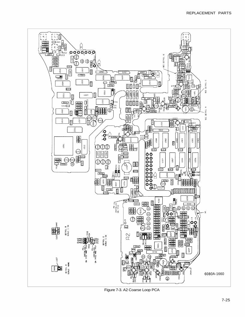
REPLACEMENT PARTS
7-25
Figure 7-3. A2 Coarse Loop PCA
6080A-1660
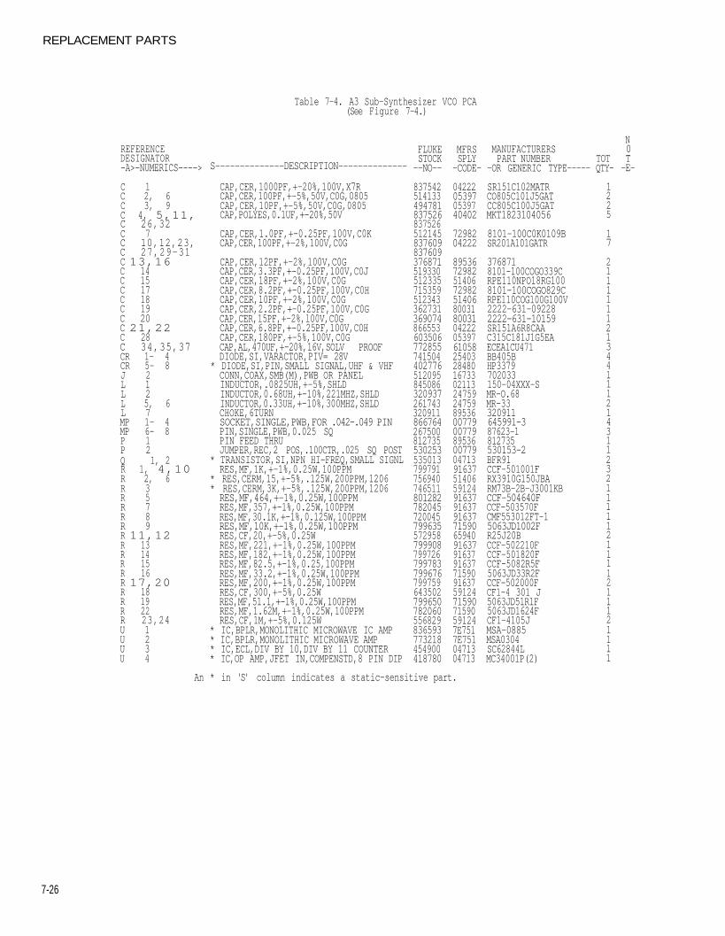
REPLACEMENT PARTS
7-26
Table 7-4. A3 Sub-Synthesizer VCO PCA(See Figure 7-4.)
REFERENCEDESIGNATOR-A>-NUMERICS---->
C 1C 2, 6C 3, 9C 4, 5,11,C 26,32C 7C 10,12,23,C 27,29-31C 13,16C 14C 15C 17C 18C 19C 20C 21,22C 28C 34,35,37CR 1- 4CR 5- 8J 2L 1L 2L 5, 6L 7MP 1- 4MP 6- 8P 1P 2Q 1, 2R 1, 4,10R 2, 6R 3R 5R 7R 8R 9R 11,12R 13R 14R 15R 16R 17,20R 18R 19R 22R 23,24U 1U 2U 3U 4
S--------------DESCRIPTION--------------
CAP,CER,1000PF,+-20%,100V,X7RCAP,CER,100PF,+-5%,50V,C0G,0805CAP,CER,10PF,+-5%,50V,C0G,0805CAP,POLYES,0.1UF,+-20%,50V
CAP,CER,1.0PF,+-0.25PF,100V,C0KCAP,CER,100PF,+-2%,100V,C0G
CAP,CER,12PF,+-2%,100V,C0GCAP,CER,3.3PF,+-0.25PF,100V,C0JCAP,CER,18PF,+-2%,100V,C0GCAP,CER,8.2PF,+-0.25PF,100V,C0HCAP,CER,10PF,+-2%,100V,C0GCAP,CER,2.2PF,+-0.25PF,100V,C0GCAP,CER,15PF,+-2%,l00V,C0GCAP,CER,6.8PF,+-0.25PF,100V,C0HCAP,CER,180PF,+-5%,100V,C0GCAP,AL,470UF,+-20%,16V,SOLV PROOFDIODE,SI,VARACTOR,PIV= 28V
* DIODE,SI,PIN,SMALL SIGNAL,UHF & VHFCONN,COAX,SMB(M),PWB OR PANELINDUCTOR,.0825UH,+-5%,SHLDINDUCTOR,0.68UH,+-10%,221MHZ,SHLDINDUCTOR,0.33UH,+-10%,300MHZ,SHLDCHOKE,6TURNSOCKET,SINGLE,PWB,FOR .042-.049 PINPIN,SINGLE,PWB,0.025 SQPIN FEED THRUJUMPER,REC,2 POS,.100CTR,.025 SQ POST
* TRANSISTOR,SI,NPN HI-FREQ,SMALL SIGNLRES,MF,1K,+-1%,0.25W,100PPM
* RES,CERM,15,+-5%,.125W,200PPM,1206* RES,CERM,3K,+-5%,.125W,200PPM,1206RES,MF,464,+-1%,0.25W,100PPMRES,MF,357,+-1%,0.25W,100PPMRES,MF,30.1K,+-1%,0.125W,100PPMRES,MF,10K,+-1%,0.25W,100PPMRES,CF,20,+-5%,0.25WRES,MF,221,+-1%,0.25W,100PPMRES,MF,182,+-1%,0.25W,100PPMRES,MF,82.5,+-1%,0.25,100PPMRES,MF,33.2,+-1%,0.25W,100PPMRES,MF,200,+-1%,0.25W,100PPMRES,CF,300,+-5%,0.25WRES,MF,51.1,+-1%,0.25W,100PPMRES,MF,1.62M,+-1%,0.25W,100PPMRES,CF,1M,+-5%,0.125W
* IC,BPLR,MONOLITHIC MICROWAVE IC AMP* IC,BPLR,MONOLITHIC MICROWAVE AMP* IC,ECL,DIV BY 10,DIV BY 11 COUNTER* IC,OP AMP,JFET IN,COMPENSTD,8 PIN DIP
FLUKESTOCK--NO--
837542514133494781837526837526512145837609837609376871519330512335715359512343362731369074866553603506772855741504402776512095845086320937261743320911866764267500812735530253535013799791756940746511801282782045720045799635572958799908799726799783799676799759643502799650782060556829836593773218454900418780
MFRSSPLY-CODE-
04222053970539740402
7298204222
8953672982514067298251406800318003104222053976105825403284801673302113247592475989536007790077989536007790471391637514065912491637916379163771590659409163791637916377159091637591247159071590591247E7517E7510471304713
MANUFACTURERSPART NUMBER
-OR GENERIC TYPE-----
SR151C102MATRCO805C101J5GATCC805C100J5GATMKT1823104056
8101-100C0K0109BSR201A101GATR
3768718101-100COGO339CRPE110NPO18RG1008101-100COGO829CRPE110COG100G100V2222-631-092282222-631-10159SR151A6R8CAAC315C181J1G5EAECEA1CU471BB405BHP3379702033150-04XXX-SMR-O.68MR-33320911645991-387623-1812735530153-2BFR91CCF-501001FRX3910G150JBARM73B-2B-J3001KBCCF-504640FCCF-503570FCMF553012FT-15063JD1002FR25J20BCCF-502210FCCF-501820FCCF-5082R5F5063JD33R2FCCF-502000FCF1-4 301 J5063JD51R1F5063JD1624FCF1-4105JMSA-0885MSA0304SC62844LMC34001P(2)
TOTQTY-
1225
17
2111111213441112143112321111121111211121111
N0T-E-
An * in 'S' column indicates a static-sensitive part.
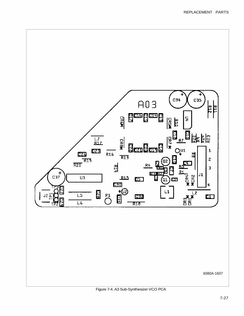
REPLACEMENT PARTS
7-27
Figure 7-4. A3 Sub-Synthesizer VCO PCA
6080A-1607
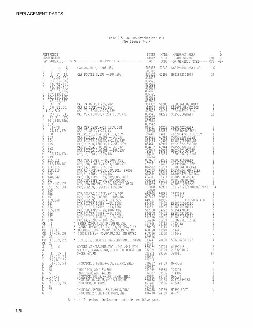
REPLACEMENT PARTS
7-28
Table 7-5. A4 Sub-Synthesizer PCA(See Figure 7-5.)
REFERENCEDESIGNATOR-A>-NUMERICS---->
C 1, 2, 4,C 5, 7, 8C 3, 17, 19,C 25,26,28,C 29,32,36,C 40,72-75,C 80,90-94,C 99,102,116,C 117,149,151,C 152,154,163,C 168,172,177C 6, 9C 10,11,31C 12,50C 27,33,34,C 70,71, 97,C 101,148,150,C 153C 76-78C 79,171,174C 98C 103C 104C 105C 106C 107C 109,173,176,C 179C 110,111C 112,180,181C 114,115C 118,119C 120C 140,142C 141C 143-147,175C 155,158,164,C 169C 156C 157C 159,160C 161C 162C 165,170C 166C 167C 178CR 1CR 11CR 12,13CR 14-16,20,CR 21CR 18,19,22,CR 23J 2, 6J 7L 1, 3- 8,L 13,33,74,L 77,81-84L 51-55,58,L 59L 56L 57L 60-62L 70,71L 72,73,79,L 80L 75L 76
S--------------DESCRIPTION--------------
CAP,AL,10UF,+-20%,35V
CAP,POLYES,0.1UF,+-20%,50V
CAP,TA,82UF,+-20%,20VCAP,AL,10UF,+-20%,16VCAP,TA,150UF,+-20%,15VCAP,CER,1000PF,+-20%,100V,X7R
CAP,CER,22PF,+-2%,100V,C0GCAP,TA,39UF,+-20%,6VCAP,POLYES,0.47UF,+-10%,50VCAP,POLYCA,0.022UF,+-5%,63VCAP,POLYPR,7500PF,+-2.5%,63VCAP,POLYPR,1500PF,+-2.5%,100VCAP,POLYCA,0.056UF,+-5%,63VCAP,POLYCA,0.027UF,+-10%,63VCAP,TA,10UF,+-20%,10V
CAP,CER,100PF,+-2%,100V,C0GCAP,CER,0.01UF,+-20%,100V,X7RCAP,TA,10UF,+-20%,35VCAP,AL,47UF,+-20%,50V,SOLV PROOFCAP,AL,47UF,+-20%,10VCAP,CER,10PF,+-5%,50V,C0G,0805CAP,CER,18PF,+-5%,50V,C0G,0805CAP,CER,1000PF,+-20%,50V,X7R,0805CAP,POLYES,0.22UF,+-10%,50V
CAP,POLYES,0.15UF,+-10%,50VCAP,POLYES,0.033UF,+-10%,50VCAP,POLYES,0.1UF,+-10%,50VCAP,POLYPR,100PF,+-1%,100VCAP,POLYPR,470PF,+-1%,100VCAP,CER,47PF,+-2%,100V,C0GCAP,POLYPR,330PF,+-1%,100VCAP,POLYPR,1000PF,+-1%,100VCAP,TA,2.2UF,+-10%,15V
* ZENER,COMP,6.3V,3%,10PPM,2MA* ZENER,UNCOMP,10.0V,10%,20.0MA,0.4W* DIODE,SI,BV= 75.0V,IO=150MA,500MW* DIODE,SI,BV= 75.0V,RADIAL INSERTED
* DIODE,SI,SCHOTTKY BARRIER,SMALL SIGNL
SOCKET,SINGLE,PWB,FOR .042-.049 PINSOCKET,SINGLE,PWB,FOR 0.034-0.037 PINCHOKE,6TURN
INDUCTOR,0.68UH,+-10%,221MHZ,SHLD
INDUCTOR,ADJ 33.8MHINDUCTOR,ADJ 44.2MHINDUCTOR,100UH,+-10%,12MHZ,SHLDINDUCTOR,0.033UH,+-10%,1000MHZINDUCTOR,10 TURNS
INDUCTOR,390UH,+-5%,6.9MHZ,SHLDINDUCTOR,270UH,+-5%,8MHZ,SHLD
FLUKESTOCK--NO--
603985603985837526837526837526837526837526837526837526837526837526357392614859422576837542837542837542837542866421163915697409854492854489854641854497720979176214176214837609407361816512822403613984494781514224514059706028706028682955696476649913844803844811512368844808844816364216357848180406698720659516659516313247313247866764732826320911320911320911320937320937774299774307249102866632463448463448186288186270
MFRSSPLY-CODE-
62643
40402
56289626433143304222
042225628984411659644040268919659646891956289
042220422256289626436264305397952750539760935
96881968816093540402404020422240402404025628904713047136594003508
28480
007790077989536
24759
8953689536247595276389536
2475924759
MANUFACTURERSPART NUMBER
-OR GENERIC TYPE-----
LL35VB106RM5X11C3
MKT1823104056
196D826X00200MA3LL16VB10RM5X11CST362D157M015ASSR151C102MATR
SR201A220GATR196D396X0006KA1J1320R47MF10PCT50VCMK5223J63L29BKP1830752062.5%FKP21522.5%100VCMK5563J63L29BMKC2-273-K-63V196D106X0010KA1
SR201A101GATR3419-1000-103M199D106X9035DA1KME50VB47RM6X11RPLL10VB47RM6X11C3CC805C100J5GATVJ0805Q180JXATC0805C102M5XAT185-2/.22/K/0050/R/C/B
IR87154KIR67333K185-0.1-K-0050-R-A-BKP1830101011%KP1830471011%SR15A470GATKP1830331011%KP1830102011%196D225X0015HA11N4578A1N7581N44481N4448
5082-6264 T25
645991-32-332070-7320911
MR-O. 68
774299774307MR-1005087226-323463448
MR390 5PCTWEE270
TOTQTY-
6
32
23210
331111114
232212164
1121121111125
4
21
15
7
11324
11
N0T-E-
An * in 'S' column indicates a static-sensitive part.
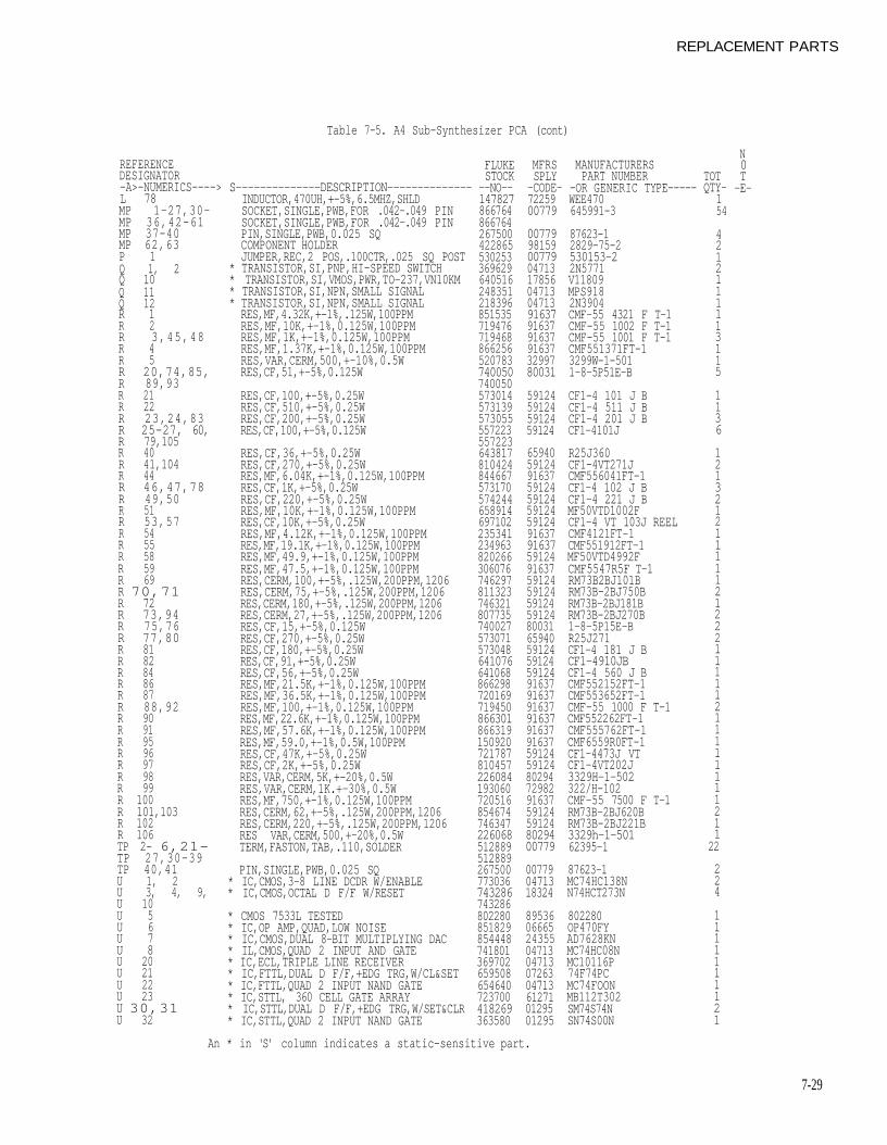
REPLACEMENT PARTS
7-29
Table 7-5. A4 Sub-Synthesizer PCA (cont)
REFERENCEDESIGNATOR-A>-NUMERICS---->L 78MP 1-27,30-MP 36,42-61MP 37-40MP 62,63P 1Q 1, 2Q 10Q 11Q 12R 1R 2R 3,45,48R 4R 5R 20,74,85,R 89,93R 21R 22R 23,24,83R 25-27, 60,R 79,105R 40R 41,104R 44R 46,47,78R 49,50R 51R 53,57R 54R 55R 58R 59R 69R 70,71R 72R 73,94R 75,76R 77,80R 81R 82R 84R 86R 87R 88,92R 90R 91R 95R 96R 97R 98R 99R 100R 101,103R 102R 106TP 2- 6,21-TP 27,30-39TP 40,41U 1, 2U 3, 4, 9,U 10U 5U 6U 7U 8U 20U 21U 22U 23U 30,31U 32
S--------------DESCRIPTION--------------INDUCTOR,470UH,+-5%,6.5MHZ,SHLDSOCKET,SINGLE,PWB,FOR .042-.049 PINSOCKET,SINGLE,PWB,FOR .042-.049 PINPIN,SINGLE,PWB,0.025 SQCOMPONENT HOLDERJUMPER,REC,2 POS,.100CTR,.025 SQ POST
* TRANSISTOR,SI,PNP,HI-SPEED SWITCH* TRANSISTOR,SI,VMOS,PWR,TO-237,VN10KM* TRANSISTOR,SI,NPN,SMALL SIGNAL* TRANSISTOR,SI,NPN,SMALL SIGNALRES,MF,4.32K,+-1%,.125W,100PPMRES,MF,10K,+-1%,0.125W,100PPMRES,MF,1K,+-1%,0.125W,100PPMRES,MF,1.37K,+-1%,0.125W,100PPMRES,VAR,CERM,500,+-10%,0.5WRES,CF,51,+-5%,0.125W
RES,CF,100,+-5%,0.25WRES,CF,510,+-5%,0.25WRES,CF,200,+-5%,0.25WRES,CF,100,+-5%,0.125W
RES,CF,36,+-5%,0.25WRES,CF,270,+-5%,0.25WRES,MF,6.04K,+-1%,0.125W,100PPMRES,CF,1K,+-5%,0.25WRES,CF,220,+-5%,0.25WRES,MF,10K,+-1%,0.125W,100PPMRES,CF,10K,+-5%,0.25WRES,MF,4.12K,+-1%,0.125W,100PPMRES,MF,19.1K,+-1%,0.125W,100PPMRES,MF,49.9,+-1%,0.125W,100PPMRES,MF,47.5,+-1%,0.125W,100PPMRES,CERM,100,+-5%,.125W,200PPM,1206RES,CERM,75,+-5%,.125W,200PPM,1206RES,CERM,180,+-5%,.125W,200PPM,1206RES,CERM,27,+-5%,.125W,200PPM,1206RES,CF,15,+-5%,0.125WRES,CF,270,+-5%,0.25WRES,CF,180,+-5%,0.25WRES,CF,91,+-5%,0.25WRES,CF,56,+-5%,0.25WRES,MF,21.5K,+-1%,0.125W,100PPMRES,MF,36.5K,+-1%,0.125W,100PPMRES,MF,100,+-1%,0.125W,100PPMRES,MF,22.6K,+-1%,0.125W,100PPMRES,MF,57.6K,+-l%,0.125W,100PPMRES,MF,59.0,+-1%,0.5W,100PPMRES,CF,47K,+-5%,0.25WRES,CF,2K,+-5%,0.25WRES,VAR,CERM,5K,+-20%,0.5WRES,VAR,CERM,1K.+-30%,0.5WRES,MF,750,+-1%,0.125W,100PPMRES,CERM,62,+-5%,.125W,200PPM,l206RES,CERM,220,+-5%,.125W,200PPM,1206RES VAR,CERM,500,+-20%,0.5WTERM,FASTON,TAB,.110,SOLDER
PIN,SINGLE,PWB,0.025 SQ* IC,CMOS,3-8 LINE DCDR W/ENABLE* IC,CMOS,OCTAL D F/F W/RESET
* CMOS 7533L TESTED* IC,OP AMP,QUAD,LOW NOISE* IC,CMOS,DUAL 8-BIT MULTIPLYING DAC* IL,CMOS,QUAD 2 INPUT AND GATE* IC,ECL,TRIPLE LINE RECEIVER* IC,FTTL,DUAL D F/F,+EDG TRG,W/CL&SET* IC,FTTL,QUAD 2 INPUT NAND GATE* IC,STTL, 360 CELL GATE ARRAY* IC,STTL,DUAL D F/F,+EDG TRG,W/SET&CLR* IC,STTL,QUAD 2 INPUT NAND GATE
FLUKESTOCK
--NO--147827866764866764267500422865530253369629640516248351218396851535719476719468866256520783740050740050573014573139573055557223557223643817810424844667573170574244658914697102235341234963820266306076746297811323746321807735740027573071573048641076641068866298720169719450866301866319150920721787810457226084193060720516854674746347226068512889512889267500773036743286743286802280851829854448741801369702659508654640723700418269363580
MFRSSPLY
-CODE-7225900779
00779981590077904713178560471304713916379163791637916373299780031
59124591245912459124
6594059124916375912459124591245912491637916375912491637591245912459124591248003165940591245912459124916379163791637916379163791637591245912480294729829163759124591248029400779
007790471318324
89536066652435504713047130726304713612710129501295
MANUFACTURERSPART NUMBER
-OR GENERIC TYPE-----WEE470645991-3
87623-12829-75-2530153-22N5771V11809MPS9182N3904CMF-55 4321 F T-1CMF-55 1002 F T-1CMF-55 1001 F T-1CMF551371FT-13299W-1-5011-8-5P51E-B
CF1-4 101 J BCF1-4 511 J BCF1-4 201 J BCF1-4101J
R25J360CF1-4VT271JCMF556041FT-1CF1-4 102 J BCF1-4 221 J BMF50VTD1002FCF1-4 VT 103J REELCMF4121FT-1CMF551912FT-1MF50VTD4992FCMF5547R5F T-1RM73B2BJ101BRM73B-2BJ750BRM73B-2BJ181BRM73B-2BJ270B1-8-5P15E-BR25J271CF1-4 181 J BCF1-4910JBCF1-4 560 J BCMF552152FT-1CMF553652FT-1CMF-55 1000 F T-1CMF552262FT-1CMF555762FT-1CMF6559R0FT-1CF1-4473J VTCF1-4VT202J3329H-1-502322/H-102CMF-55 7500 F T-1RM73B-2BJ620BRM73B-2BJ221B3329h-1-50162395-1
87623-1MC74HC138NN74HCT273N
802280OP470FYAD7628KNMC74HC08NMC10116P74F74PCMC74FOONMB112T302SM74S74NSN74S00N
TOTQTY-154
4212111113115
1136
1213212111112122211111211111111211
22
224
1111111121
N0T-E-
An * in 'S' column indicates a static-sensitive part.
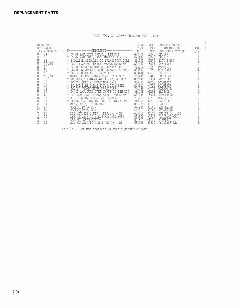
Table 7-5. A4 Sub-Synthesizer PCA (cont)
REFERENCEDESIGNATOR-A>-NUMERICS---->UUUUUUUUUUUUUUUUWXUXUZZZZ
34353637,6050515253,5455565758596162631
236210202122
S--------------DESCRIPTION--------------* IC,OP AMP,JFET INPUT,8 PIN DIP* IC,OP AMP,DUAL, JFET INPUT,8 PIN DIP* ISOLATOR,OPTO,LED TO TRANSISTOR,DUAL* IC,FTTL,SYNC PRESET DECADE COUNTER* IC,BPLR,MONOLITHIC MICROWAVE AMP* IC,BPLR,MONOLITHIC MICROWAVE IC AMP* 3DB COUPLER FOR SUBSYNTHMIXER,DOUBLE BALANCED,l - 500 MHZ
* IC,BPLR,WIDEBAND AMPLIFIER,600 MHZ* IC,ECL,QUAD 2 INPUT NOR GATE* IC,ECL,DUAL D M/S F/F,W/SET&RESET* IC,ECL,TWO-MODULUS PRESCALER* IC,OP AMP,QUAD,JFET INPUT,14 PIN DIP* IC, CMOS,DUAL DECADE RIPPLE COUNTER* IC,STTL,360 CELL GATE ARRAY* IC,ARRAY,5 TRANS,5 ISO: 2-PNP,3-NPNCABLE ASSY, RF JUMPERSOCKET,IC,24 PINSOCKET,IC,28 PINRES,NET,SIP,8 PIN,7 RES,560,+-2%RES,NET,SIP,10 PIN,9 RES,510,+-2%RES,NET,CERM,CUSTOMRES,NET,SIP,10 PIN,5 RES,1K,+-2%
FLUKESTOCK--NO--472779495192454330854450773218836593860648733105854542380881454959722298483438854349723718418954861083376236448217484451478800501841655209
MFRSSPLY-CODE-120401204050579183247E7517E7518953616469183240471304713047130129518324612710273589536915069150691637916370112191637
MANUFACTURERSPART NUMBER
-OR GENERIC TYPE---LF356NLF353NILCT-6-25474F160ANMSA0304MSA-0885860648SBL-1-27NE5205NMC10102PMC10131PMC12011LTL084CN74HCT390NMB112T301CA3096E861083224-AG39D228-AG39DCSC08A-01-561GCSC10A-01-511316B103FCSC10B03102G
TOT-- QTY-
11121112111111111111111
N0T-E-
An * in 'S' column indicates a static-sensitive part.
REPLACEMENT PARTS
7-30
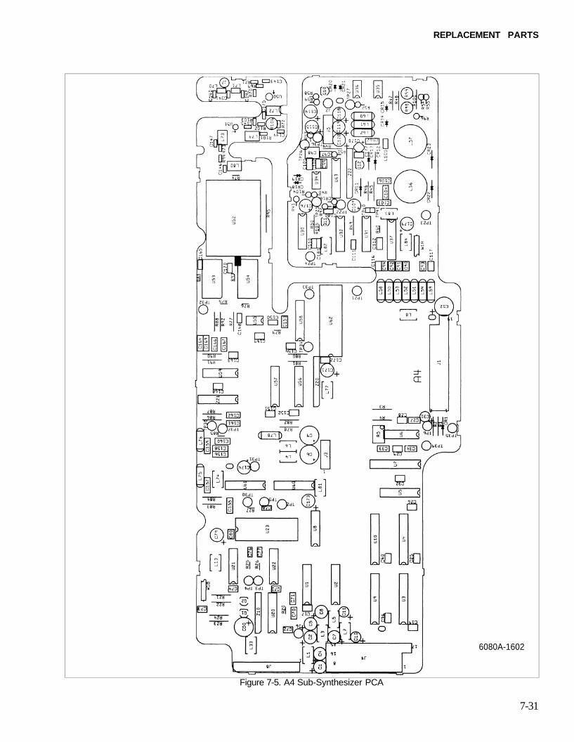
REPLACEMENT PARTS
Figure 7-5. A4 Sub-Synthesizer PCA
7-31
6080A-1602
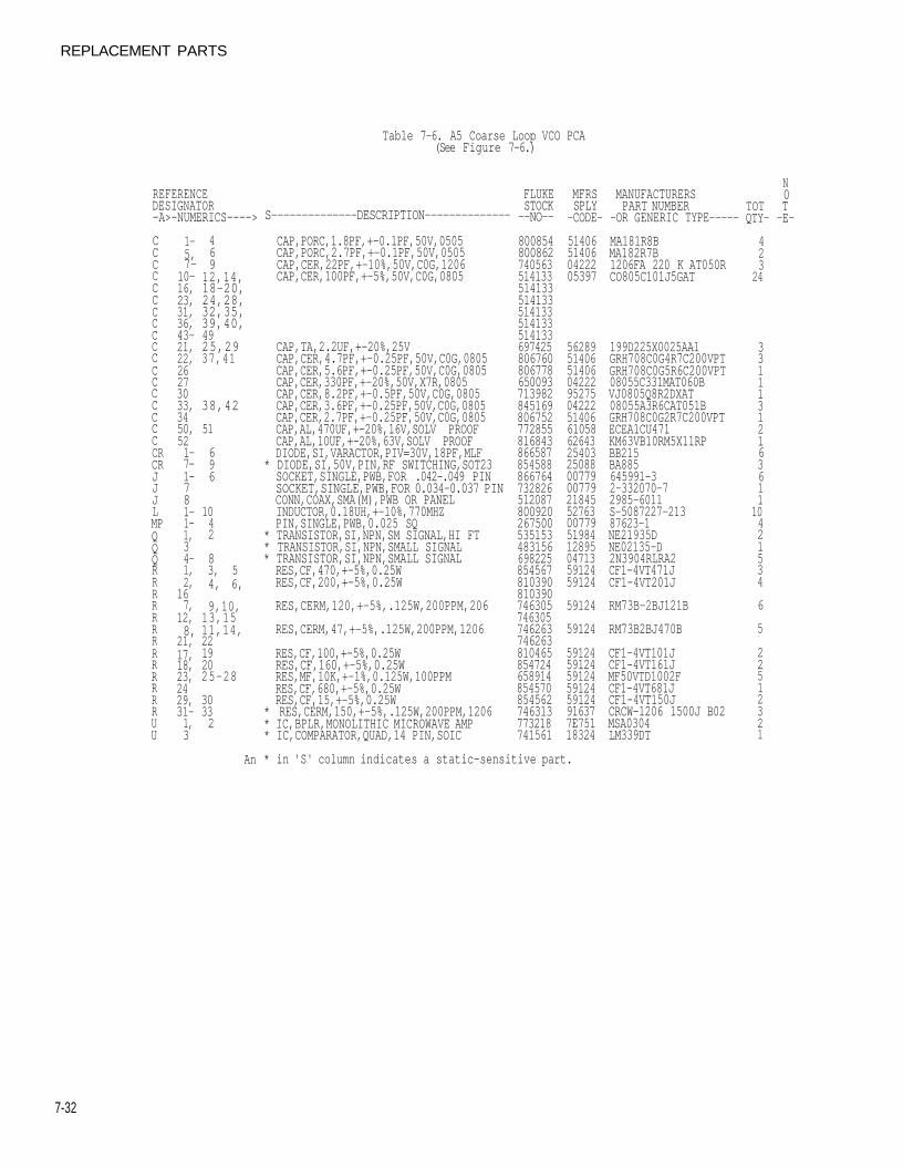
REPLACEMENT PARTS
7-32
Table 7-6. A5 Coarse Loop VCO PCA(See Figure 7-6.)
REFERENCEDESIGNATOR-A>-NUMERICS---->
CCCCCCCCCCCCCCCCCCCRCRJJJLMPQQQRRRRRRRRRRRRRUU
1-5,7-
10-16,23,31,36,43-21,22,26273033,3450,521-7-1-781-1-1,34-1,2,
167,
12,8,
21,17,18,23,2429,31-1,3
469
12,14,18-20,24,28,32,35,39,40,4925,2937,41
38,42
51
696
1042
83, 54, 6,
9,10,13,1511,14,22192025-28
30332
An
S--------------DESCRIPTION--------------
CAP,PORC,1.8PF,+-0.1PF,50V,0505CAP,PORC,2.7PF,+-0.1PF,50V,0505CAP,CER,22PF,+-10%,50V,C0G,1206CAP,CER,100PF,+-5%,50V,C0G,0805
CAP,TA,2.2UF,+-20%,25VCAP,CER,4.7PF,+-0.25PF,50V,C0G,0805CAP,CER,5.6PF,+-0.25PF,50V,C0G,0805CAP,CER,330PF,+-20%,50V,X7R,0805CAP,CER,8.2PF,+-0.5PF,50V,C0G,0805CAP,CER,3.6PF,+-0.25PF,50V,C0G,0805CAP,CER,2.7PF,+-0.25PF,50V,C0G,0805CAP,AL,470UF,+-20%,16V,SOLV PROOFCAP,AL,10UF,+-20%,63V,SOLV PROOFDIODE,SI,VARACTOR,PIV=30V,18PF,MLF
* DIODE,SI,50V,PIN,RF SWITCHING,SOT23SOCKET,SINGLE,PWB,FOR .042-.049 PINSOCKET,SINGLE,PWB,FOR 0.034-0.037 PINCONN,COAX,SMA(M),PWB OR PANELINDUCTOR,0.18UH,+-10%,770MHZPIN,SINGLE,PWB,0.025 SQ
* TRANSISTOR,SI,NPN,SM SIGNAL,HI FT* TRANSISTOR,SI,NPN,SMALL SIGNAL* TRANSISTOR,SI,NPN,SMALL SIGNALRES,CF,470,+-5%,0.25WRES,CF,200,+-5%,0.25W
RES,CERM,120,+-5%,.125W,200PPM,206
RES,CERM,47,+-5%,.125W,200PPM,1206
RES,CF,100,+-5%,0.25WRES,CF,160,+-5%,0.25WRES,MF,10K,+-1%,0.125W,100PPMRES,CF,680,+-5%,0.25WRES,CF,15,+-5%,0.25W
* RES,CERM,150,+-5%,.125W,200PPM,1206* IC,BPLR,MONOLITHIC MICROWAVE AMP* IC,COMPARATOR,QUAD,14 PIN,SOIC
FLUKESTOCK--NO--
800854800862740563514133514133514133514133514133514133697425806760806778650093713982845169806752772855816843866587854588866764732826512087800920267500535153483156698225854567810390810390746305746305746263746263810465854724658914854570854562746313773218741561
MFRSSPLY-CODE-
MANUFACTURERSPART NUMBER
-OR GENERIC TYPE-----
51406 MA181R8B514060422205397
562895140651406042229527504222514066105862643254032508800779007792184552763007795198412895047135912459124
59124
59124
5912459124591245912459124916377E75118324
MA182R7B1206FA 220 K AT050RCO805C101J5GAT
199D225X0025AA1GRH708C0G4R7C200VPTGRH708C0G5R6C200VPT08055C331MAT060BVJ0805Q8R2DXAT08055A3R6CAT051BGRH708C0G2R7C200VPTECEA1CU471KM63VB10RM5X11RPBB215BA885645991-32-332070-72985-6011S-5087227-21387623-1NE21935DNE02135-D2N3904RLRA2CF1-4VT471JCF1-4VT201J
RM73B-2BJ121B
RM73B2BJ470B
CF1-4VT101JCF1-4VT161JMF50VTD1002FCF1-4VT681JCF1-4VT150JCRCW-1206 1500J B02MSA0304LM339DT
N0
TOT TQTY- -E-
423
24
33111312163611
10421534
6
5
22512321
* in 'S' column indicates a static-sensitive part.
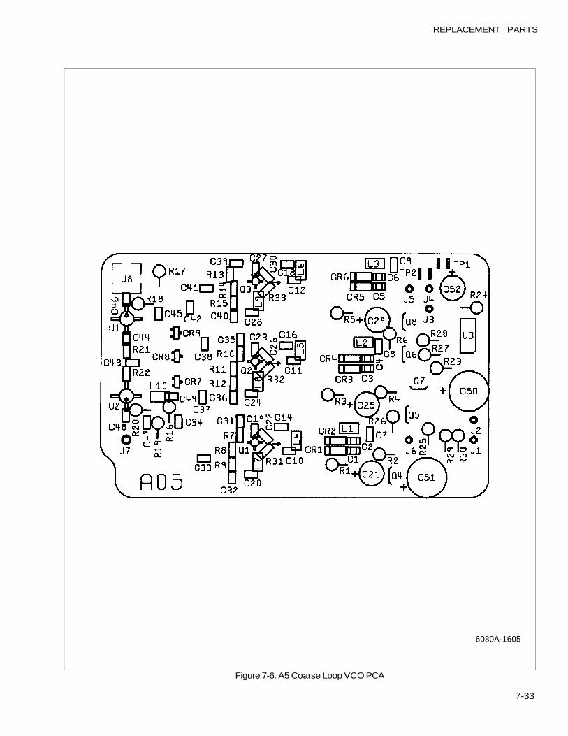
REPLACEMENT PARTS
Figure 7-6. A5 Coarse Loop VCO PCA
7-33
6080A-1605
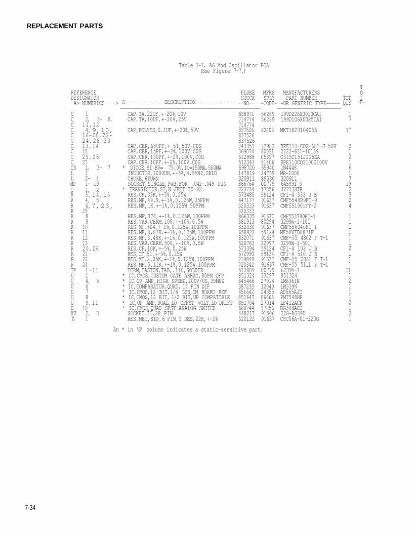
REPLACEMENT PARTS
7-34
Table 7-7. A6 Mod Oscillator PCA(See Figure 7-7.)
REFERENCEDESIGNATOR-A>-NUMERICS---->
CCCCCCCCCCCRLLMPQRRRRRRRRRRRRRRTPUUUUUUUXUZ
12, 5- 8,11,124, 9,10,
16-20,22-24,28-3313,141525,26271, 3- 712- 41- 191, 23,14,154, 56, 7,23,
2589
1011121320,262122241-1114, 56789,11
102, 31
S--------------DESCRIPTION--------------
CAP,TA,22UF,+-20%,10VCAP,TA,10UF,+-20%,25V
CAP,POLYES,0.1UF,+-20%,50V
CAP,CER,680PF,+-5%,50V,C0GCAP,CER,15PF,+-2%,100V,C0GCAP,CER,150PF,+-2%,100V,C0GCAP,CER,10PF,+-2%,100V,C0G
* DIODE,SI,BV= 75.0V,IO=150MA,500MWINDUCTOR,1000UH,+-5%,4.5MHZ,SHLDCHOKE,6TURNSOCKET,SINGLE,PWB,FOR .042-.049 PIN
* TRANSISTOR,SI,N-JFET,TO-92RES,CF,33K,+-5%,0.25WRES,MF,49.9,+-1%,0.125W,25PPMRES,MF,1K,+-1%,0.125W,50PPM
RES,MF,374,+-1%,0.125W,100PPMRES,VAR,CERM,100,+-10%,0.5WRES,MF,604,+-1%,0.125W,100PPMRES,MF,8.87K,+-1%,0.125W,100PPMRES,MF,3.48K,+-1%,0.125W,100PPMRES,VAR,CERM,500,+-10%,0.5WRES,CF,10K,+-5%,0.25WRES,CF,51,+-5%,0.25WRES,MF,2.05K,+-1%,0.125W,100PPMRES,MF,5.11K,+-1%,0.125W,100PPMTERM,FASTON,TAB,.110,SOLDER
* IC,CMOS,CUSTOM GATE ARRAY,80PN QFP* IC,OP AMP,HIGH SPEED,200V/US,35MHZ* IC,COMPARATOR,QUAD, 14 PIN DIP* IC,CMOS,12 BIT,1/4 LSB,ON BOARD REF* IC,CMOS,12 BIT, 1/2 BIT,UP COMPATIBLE* IC,OP AMP,DUAL,LO OFFST VOLT,LO-DRIFT* IC,CMOS,QUAD SPST ANALOG SWITCHSOCKET,IC,28 PINRES,NET,SIP,6 PIN,5 RES,22K,+-2%
FLUKESTOCK--NO--
658971714774714774837526837526837526743351369074512988512343698720147819320911866764723734573485447177320333320333866335381913832030658922832071520783573394572990719849720342512889851324845466387233851642851647851704680744448217520122
MFRSSPLY-CODE-
5628956289
40402
729828003105397514066594024759895360077917856591249163791637
9163780294916375912491637329975912459124916379163700779332972701412040243550666527014178569150691637
MANUFACTURERSPART NUMBER
-OR GENERIC TYPE-----
199D226X0010CA1199D106X0025CA1
MKT1823104056
RPE113-COG-681-J-50V2222-631-10159C315C151J1G5EARPE110COG100G100V1N4448MR-1000320911645991-3J27138TRCF1-4 333 J BCMF5549R9FT-9CMF551001FT-2
CMF553740FT-13299W-1-101CMF556040FT-1MF50VTD8871FCMF-55 4802 F T-13299W-1-501CF1-4 103 J BCF1-4 510 J BCMF-55 2051 F T-1CMF-55 5111 F T-162395-1851324LM6361NLM339NAD565AJDPM7548HPLF412ACNDG308ACJ228-AG39DCSC06A-01-223G
TOTQTY-
17
17
2121613192324
1111112111
11121112121
N0T-E-
An * in 'S' column indicates a static-sensitive part.
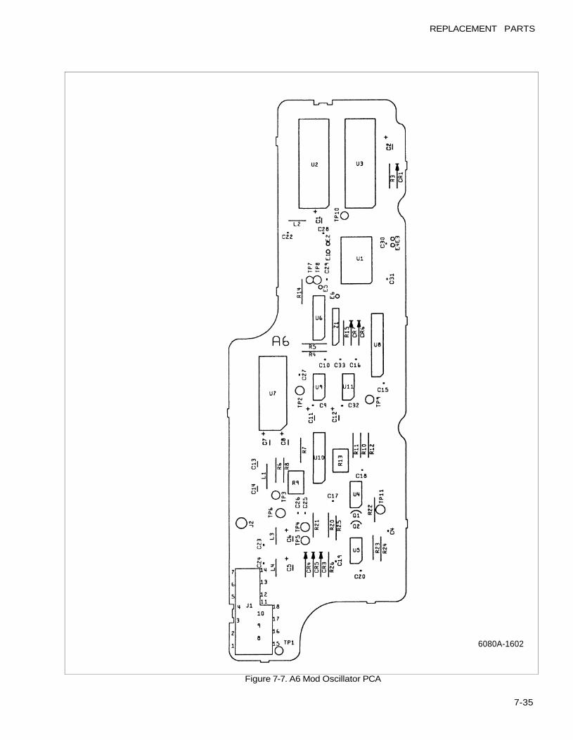
REPLACEMENT PARTS
7-35
Figure 7-7. A6 Mod Oscillator PCA
6080A-1602
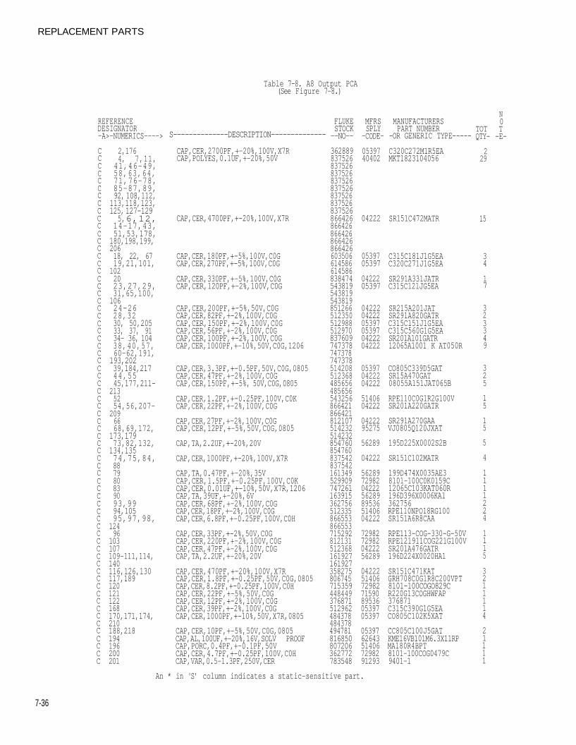
REPLACEMENT PARTS
7-36
Table 7-8. A8 Output PCA(See Figure 7-8.)
REFERENCEDESIGNATOR-A>-NUMERICS---->
CCCCCCCCCCCCCCCCCCCCCCCCCCCCCCCCCCCCCCCCCCCCCCCCCCCCCCCCCCCCCCCCCCCCC
2,1764, 7,11,
41,46-49,58,63,64,71,76-78,85-87,89,92, 108,112,
113,118,123,125, 127-129
5, 6,12,14-17,43,51,53,178,
180,198,199,20618, 22, 6719,21,101,1022023,27,29,31,65,100,10624-2628,3230, 50,20533, 37, 9134- 36, 10438,40,57,60-62,191,193,20239,184,21744,5545,177,211-
2135254,56,207-2096668,69,172,173,17973,82,132,134,13574,75,84,887980839093,9994,10595,97,98,
12496
103107109-111,114,140116,126,130117,189120121122168170,171,174,210188,218194196200201
S--------------DESCRIPTION--------------
CAP,CER,2700PF,+-20%,100V,X7RCAP,POLYES,0.1UF,+-20%,50V
CAP,CER,4700PF,+-20%,100V,X7R
CAP,CER,180PF,+-5%,100V,C0GCAP,CER,270PF,+-5%,100V,C0G
CAP,CER,330PF,+-5%,100V,C0GCAP,CER,120PF,+-2%,100V,C0G
CAP,CER,200PF,+-5%,50V,C0GCAP,CER,82PF,+-2%,100V,C0GCAP,CER,150PF,+-2%,100V,C0GCAP,CER,56PF,+-2%,100V,C0GCAP,CER,100PF,+-2%,100V,C0GCAP,CER,1000PF,+-10%,50V,C0G,1206
CAP,CER,3.3PF,+-0.5PF,50V,C0G,0805CAP,CER,47PF,+-2%,100V,C0GCAP,CER,150PF,+-5%, 50V,C0G,0805
CAP,CER,1.2PF,+-0.25PF,100V,C0KCAP,CER,22PF,+-2%,100V,C0G
CAP,CER,27PF,+-2%,100V,C0GCAP,CER,12PF,+-5%,50V,C0G,0805
CAP,TA,2.2UF,+-20%,20V
CAP,CER,1000PF,+-20%,100V,X7R
CAP,TA,0.47PF,+-20%,35VCAP,CER,1.5PF,+-0.25PF,100V,C0KCAP,CER,0.01UF,+-10%,50V,X7R,1206CAP,TA,39UF,+-20%,6VCAP,CER,68PF,+-2%,100V,C0GCAP,CER,18PF,+-2%,100V,C0GCAP,CER,6.8PF,+-0.25PF,100V,C0H
CAP,CER,33PF,+-2%,50V,C0GCAP,CER,220PF,+-2%,100V,C0GCAP,CER,47PF,+-2%,100V,C0GCAP,TA,2.2UF,+-20%,20V
CAP,CER,470PF,+-20%,100V,X7RCAP,CER,1.8PF,+-0.25PF,50V,C0G,0805CAP,CER,8.2PF,+-0.25PF,100V,C0HCAP,CER,22PF,+-5%,50V,C0GCAP,CER,12PF,+-2%,100V,C0GCAP,CER,39PF,+-2%,100V,C0GCAP,CER,1000PF,+-10%,50V,X7R,0805
CAP,CER,10PF,+-5%,50V,C0G,0805CAP,AL,100UF,+-20%,16V,SOLV PROOFCAP,PORC,0.4PF,+-0.1PF,50VCAP,CER,4.7PF,+-0.25PF,100V,C0HCAP,VAR,0.5-1.3PF,250V,CER
FLUKESTOCK--NO--
362889837526837526837526837526837526837526837526837526866426866426866426866426866426603506614586614586838474543819543819543819851266512350512988512970837609747378747378747378514208512368485656485656543256866421866421812107514232514232854760854760837542837542161349529909747261163915362756512335866553866553715292812131512368161927161927358275806745715359448449376871512962484378484378494781816850807206362772783548
MFRSSPLY
-CODE-
MANUFACTURERSPART NUMBER
-OR GENERIC TYPE-----
05397 C320C272M1R5EA40402
04222
0539705397
0422205397
042220422205397053970422204222
053970422204222
5140604222
0422295275
56289
04222
56289729820422256289895365140604222
72982729820422256289
04222514067298271590895360539705397
0539762643514067298291293
MKT1823104056
SR151C472MATR
C315C181J1G5EAC320C271J1G5EA
SR291A331JATRC315C121JG5EA
SR215A201JATSR291A820GATRC315C151J1G5EAC315C560G1G5EASR201A101GATR12065A1001 K AT050R
CO805C339D5GATSR15A470GAT08055A151JAT065B
RPE110C0G1R2G100VSR201A220GATR
SR291A270GAAVJ0805Q120JXAT
195D225X0002S2B
SR151C102MATR
199D474X0035AE38101-100C0K0159C12065C103KAT060R196D396X0006KA1362756RPE110NPO18RG100SR151A6R8CAA
RPE113-COG-330-G-50VRPE121911COG221G100VSR201A476GATR196D224X0020HA1
SR151C471KATGRH708C0G1R8C200VPT8101-100COGO829CR220G13COGHWFAP376871C315C390G1G5EACO805C102K5XAT
CC805C100J5GATKME16VB101M6.3X11RPMA180R4BPT8101-100COG0479C9401-1
N0
TOT TQTY- -E-
229
15
34
17
323349
325
15
15
5
4
1111224
1115
3211114
21111
An * in 'S' column indicates a static-sensitive part.
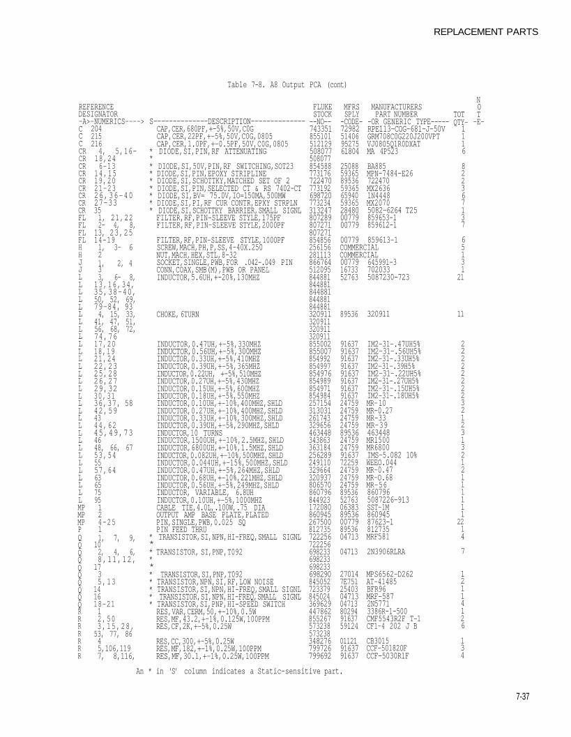
REPLACEMENT PARTS
7-37
Tab1e 7-8. A8 Output PCA (cont)
REFERENCEDESIGNATOR-A>-NUMERICS---->CCCCRCRCRCRCRCRCRCRCRFLFLFLFLHHJJLLLLLLLLLLLLLLLLLLLLLLLLLLLLLLLMPMPMPPQQQQQQQQQQRRRRRRR
2042152164, 5,16-
18,246-13
14,1519,2021-2326,36-4027-33351, 21,222- 4, 8,13, 23,2514-191, 3- 621, 2, 433, 6- 8,13,16,34,35,38-40,50, 52, 69,79-84, 934, 15, 33,
41, 47, 51,56, 68, 72,74,7617,2018,1921,2422,2325,2826,2729,3230,3136,37, 5842,594344,6245,49,734648, 66, 6753,545557,6463657595124-2511, 7, 9,
102, 4, 6,8,11,12,
1735,13
141618-2112,503,15,28,53, 77, 8645,106,1197, 8,116,
S--------------DESCRIPTION--------------CAP,CER,680PF,+-5%,50V,C0GCAP,CER,22PF,+-5%,50V,C0G,0805CAP,CER,1.0PF,+-0.5PF,50V,C0G,0805
* DIODE,SI,PIN,RF ATTENUATING** DIODE,SI,50V,PIN,RF SWITCHING,SOT23* DIODE,SI,PIN,EPOXY STRIPLINE* DIODE,SI,SCHOTTKY,MATCHED SET OF 2* DIODE,SI,PIN,SELECTED CT & RS 7402-CT* DIODE,SI,BV= 75.0V,IO=150MA,500MW* DIODE,SI,PI,RF CUR CONTR,EPXY STRPLN* DIODE,SI,SCHOTTKY BARRIER,SMALL SIGNLFILTER,RF,PIN-SLEEVE STYLE,175PFFILTER,RF,PIN-SLEEVE STYLE,2000PF
FILTER,RF,PIN-SLEEVE STYLE,1000PFSCREW,MACH,PH,P,SS,4-40X.250NUT,MACH,HEX,STL,8-32SOCKET,SINGLE,PWB,FOR .042-.049 PINCONN,COAX,SMB(M),PWB OR PANELINDUCTOR,5.6UH,+-20%,130MHZ
CHOKE, 6TURN
INDUCTOR,0.47UH,+-5%,330MHZINDUCTOR,0.56UH,+-5%,300MHZINDUCTOR,0.33UH,+-5%,410MHZINDUCTOR,0.39UH,+-5%,365MHZINDUCTOR,0.22UH, +-5%,510MHZINDUCTOR,0.27UH,+-5%,430MHZINDUCTOR,0.15UH,+-5%,600MHZINDUCTOR,0.18UH,+-5%,550MHZINDUCTOR,0.10UH,+-10%,400MHZ,SHLDINDUCTOR,0.27UH,+-10%,400MHZ,SHLDINDUCTOR,0.33UH,+-10%,300MHZ,SHLDINDUCTOR,0.39UH,+-5%,290MHZ,SHLDINDUCTOR,10 TURNSINDUCTOR,1500UH,+-10%,2.5MHZ,SHLDINDUCTOR,6800UH,+-10%,1.5MHZ,SHLDINDUCTOR,0.082UH,+-10%,500MHZ,SHLDINDUCTOR,0.044UH,+-15%,500MHZ,SHLDINDUCTOR,0.47UH,+-5%,264MHZ,SHLDINDUCTOR,0.68UH,+-10%,221MHZ,SHLDINDUCTOR,0.56UH,+-5%,249MHZ,SHLDINDUCTOR, VARIABLE, 6.8UHINDUCTOR,0.10UH,+-5%,1000MHZCABLE TIE,4.0L,.100W,.75 DIAOUTPUT AMP BASE PLATE,PLATEDPIN,SINGLE,PWB,0.025 SQPIN FEED THRU
* TRANSISTOR,SI,NPN,HI-FREQ,SMALL SIGNL** TRANSISTOR, SI,PNP,T092*** TRANSISTOR,SI,PNP,T092* TRANSISTOR,NPN,SI,RF,LOW NOISE* TRANSISTOR,SI,NPN,HI-FREQ,SMALL SIGNL* TRANSISTOR,SI,NPN,HI-FREQ,SMALL SIGNL* TRANSISTOR,SI,PNP,HI-SPEED SWITCHRES,VAR,CERM,50,+-10%,0.5WRES,MF,43.2,+-1%,0.125W,100PPMRES,CF,2K,+-5%,0.25W
RES,CC,300,+-5%,0.25WRES,MF,182,+-1%,0.25W,100PPMRES,MF,30.1,+-1%,0.25W,100PPM
FLUKESTOCK--NO--743351855101512129508077508077854588773176722470773192698720773234313247807289807271807271854856256156281113866764512095844881844881844881844881844881320911320911320911320911855002855007854992854997854976854989854971854984257154313031261743329656463448343863363184256289249110329664320937806570860796844923172080860945267500812735722256722256698233698233698233698290845052723379845024369629447862855267573238573238348276799726799692
MFRSSPLY
-CODE-72982514069527561804
250885936589536593656594059365284800077900779
00779
MANUFACTURERSPART NUMBER
-OR GENERIC TYPE-----RPE113-COG-681-J-50VGRM708C0G220J200VPTVJ0805Q1R0DXATMA 4P523
BA885MPN-7484-E26722470MX26361N4448MX20705082-6264 T25859653-1859612-1
859613-1COMMERCIALCOMMERCIAL007791673352763
89536
916379163791637916379163791637916379163724759247592475924759895362475924759916377225924759247592475989536527630638389536007798953604713
04713
270147E751254030471304713802949163759124
011219163791637
645991-37020335087230-723
320911
IM2-31-.47UH5%IM2-31-.56UH5%IM2-31-.33UH5%IM2-31-.39H5%IM2-31-.22UH5%IM2-31-.27UH5%IM2-31-.15UH5%IM2-31-.18UH5%MR- 10MR-0.27MR-33MR- 3 9463448MR1500MR6800IMS-5.082 10%WEEO.044MR-0.47MR-O.68MR- 5 68607965087226-913SST-1M86094587623-1812735MRF581
2N3906RLRA
MPS6562-D262AT-41485BFR96MRF-5872N57713386R-1-500CMF5543R2F T-1CF1-4 202 J B
CB3015CCF-501820FCCF-5030R1F
TOTQTY-1116
822367137
65131
21
11
2222222232123132121111112214
7
12114126
134
An * in 'S' column indicates a Static-sensitive part.
N0T-E-
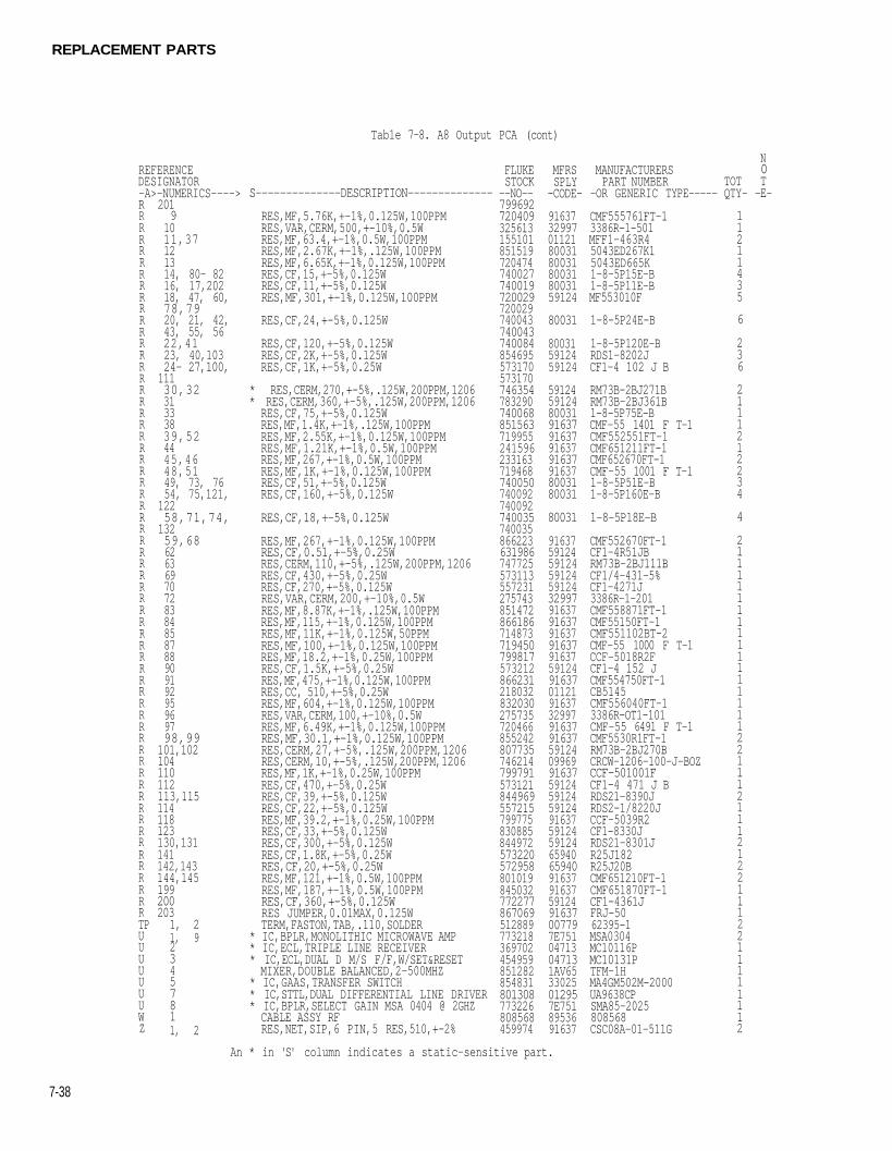
REPLACEMENT PARTS
7-38
Tab1e 7-8. A8 Output PCA (cont)
REFERENCEDESIGNATOR-A>-NUMERICS---->RRRRRRRRRRRRRRRRRRRRRRRRRRRRRRRRRRRRRRRRRRRRRRRRRRRRRRRRRRRRRRTPUUUUUUUWZ
2019
1011,37121314, 80- 8216, 17,20218, 47, 60,78,7920, 21, 42,43, 55, 5622,4123, 40,10324- 27,100,11130,3231333839,524445,4648,5149, 73, 7654, 75,121,12258,71,74,13259,686263697072838485878890919295969798,99
101,102104110112113,115114118123130,131141142,143144,1451992002031, 21, 923457811, 2
S--------------DESCRIPTION--------------
RES,MF,5.76K,+-1%,0.125W,100PPMRES,VAR,CERM,500,+-10%,0.5WRES,MF,63.4,+-1%,0.5W,100PPMRES,MF,2.67K,+-1%,.125W,100PPMRES,MF,6.65K,+-1%,0.125W,100PPMRES,CF,15,+-5%,0.125WRES,CF,11,+-5%,0.125WRES,MF,301,+-1%,0.125W,100PPM
RES,CF,24,+-5%,0.125W
RES,CF,120,+-5%,0.125WRES,CF,2K,+-5%,0.125WRES,CF,1K,+-5%,0.25W
* RES,CERM,270,+-5%,.125W,200PPM,1206* RES,CERM,360,+-5%,.125W,200PPM,1206RES,CF,75,+-5%,0.125WRES,MF,1.4K,+-1%,.125W,100PPMRES,MF,2.55K,+-1%,0.125W,100PPMRES,MF,1.21K,+-1%,0.5W,100PPMRES,MF,267,+-1%,0.5W,100PPMRES,MF,1K,+-1%,0.125W,100PPMRES,CF,51,+-5%,0.125WRES,CF,160,+-5%,0.125W
RES,CF,18,+-5%,0.125W
RES,MF,267,+-1%,0.125W,100PPMRES,CF,0.51,+-5%,0.25WRES,CERM,110,+-5%,.125W,200PPM,1206RES,CF,430,+-5%,0.25WRES,CF,270,+-5%,0.125WRES,VAR,CERM,200,+-10%,0.5WRES,MF,8.87K,+-1%,.125W,100PPMRES,MF,115,+-1%,0.125W,100PPMRES,MF,11K,+-1%,0.125W,50PPMRES,MF,100,+-1%,0.125W,100PPMRES,MF,18.2,+-1%,0.25W,100PPMRES,CF,1.5K,+-5%,0.25WRES,MF,475,+-1%,0.125W,100PPMRES,CC, 510,+-5%,0.25WRES,MF,604,+-1%,0.125W,100PPMRES,VAR,CERM,100,+-10%,0.5WRES,MF,6.49K,+-1%,0.125W,100PPMRES,MF,30.1,+-1%,0.125W,100PPMRES,CERM,27,+-5%,.125W,200PPM,1206RES,CERM,10,+-5%,.125W,200PPM,1206RES,MF,1K,+-1%,0.25W,100PPMRES,CF,470,+-5%,0.25WRES,CF,39,+-5%,0.125WRES,CF,22,+-5%,0.125WRES,MF,39.2,+-1%,0.25W,100PPMRES,CF,33,+-5%,0.125WRES,CF,300,+-5%,0.125WRES,CF,1.8K,+-5%,0.25WRES,CF,20,+-5%,0.25WRES,MF,121,+-1%,0.5W,100PPMRES,MF,187,+-1%,0.5W,100PPMRES,CF,360,+-5%,0.125WRES JUMPER,0.01MAX,0.125WTERM,FASTON,TAB,.110,SOLDER
* IC,BPLR,MONOLITHIC MICROWAVE AMP* IC,ECL,TRIPLE LINE RECEIVER* IC,ECL,DUAL D M/S F/F,W/SET&RESETMIXER,DOUBLE BALANCED,2-500MHZ
* IC,GAAS,TRANSFER SWITCH* IC,STTL,DUAL DIFFERENTIAL LINE DRIVER* IC,BPLR,SELECT GAIN MSA 0404 @ 2GHZCABLE ASSY RFRES,NET,SIP,6 PIN,5 RES,510,+-2%
FLUKESTOCK--NO--799692720409325613155101851519720474740027740019720029720029740043740043740084854695573170573170746354783290740068851563719955241596233163719468740050740092740092740035740035866223631986747725573113557231275743851472866186714873719450799817573212866231218032832030275735720466855242807735746214799791573121844969557215799775830885844972573220572958801019845032772277867069512889773218369702454959851282854831801308773226808568459974
MFRSSPLY
-CODE-
9163732997011218003180031800318003159124
80031
800315912459124
59124591248003191637916379163791637916378003180031
80031
916375912459124591245912432997916379163791637916379163759124916370112191637329979163791637591240996991637591245912459124916375912459124659406594091637916375912491637007797E75104713047131AV6533025012957E7518953691637
MANUFACTURERSPART NUMBER
-OR GENERIC TYPE-----
CMF555761FT-13386R-1-501MFF1-463R45043ED267K15043ED665K1-8-5P15E-B1-8-5P11E-BMF553010F
1-8-5P24E-B
1-8-5P120E-BRDS1-8202JCF1-4 102 J B
RM73B-2BJ271BRM73B-2BJ361B1-8-5P75E-BCMF-55 1401 F T-1CMF552551FT-1CMF651211FT-1CMF652670FT-1CMF-55 1001 F T-11-8-5P51E-B1-8-5P160E-B
1-8-5P18E-B
CMF552670FT-1CF1-4R51JBRM73B-2BJ111BCF1/4-431-5%CF1-4271J3386R-1-201CMF558871FT-1CMF55150FT-1CMF551102BT-2CMF-55 1000 F T-1CCF-5018R2FCF1-4 152 JCMF554750FT-1CB5145CMF556040FT-13386R-OT1-101CMF-55 6491 F T-1CMF5530R1FT-1RM73B-2BJ270BCRCW-1206-100-J-BOZCCF-501001FCF1-4 471 J BRDS21-8390JRDS2-1/8220JCCF-5039R2CF1-8330JRDS21-8301JR25J182R25J20BCMF651210FT-1CMF651870FT-1CF1-4361JFRJ-5062395-1MSA0304MC10116PMC10131PTFM-1HMA4GM502M-2000UA9638CPSMA85-2025808568CSC08A-01-511G
TOTQTY-
11211435
6
236
2111212234
4
2111111111111111122111211121221112211111112
N0T-E-
An * in 'S' column indicates a static-sensitive part.
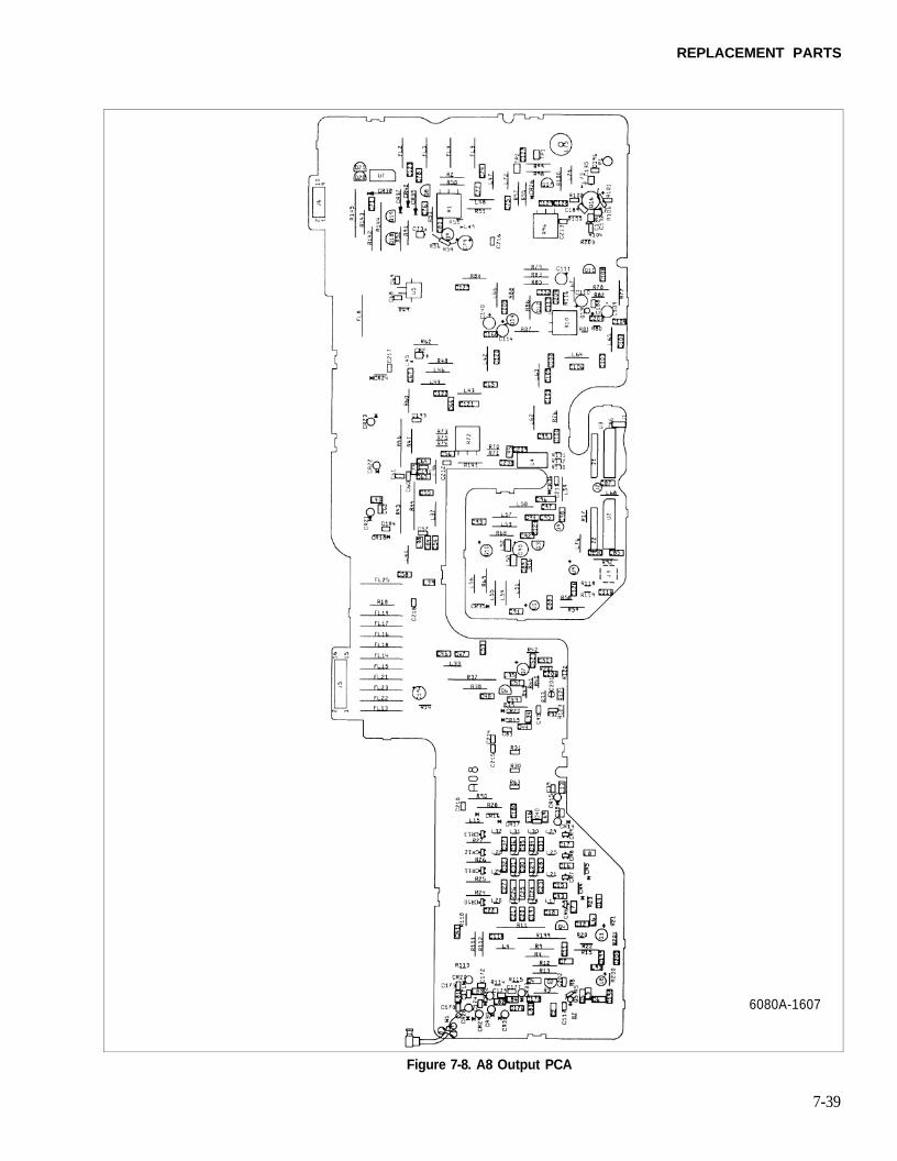
REPLACEMENT PARTS
7-39
Figure 7-8. A8 Output PCA
6080A-1607
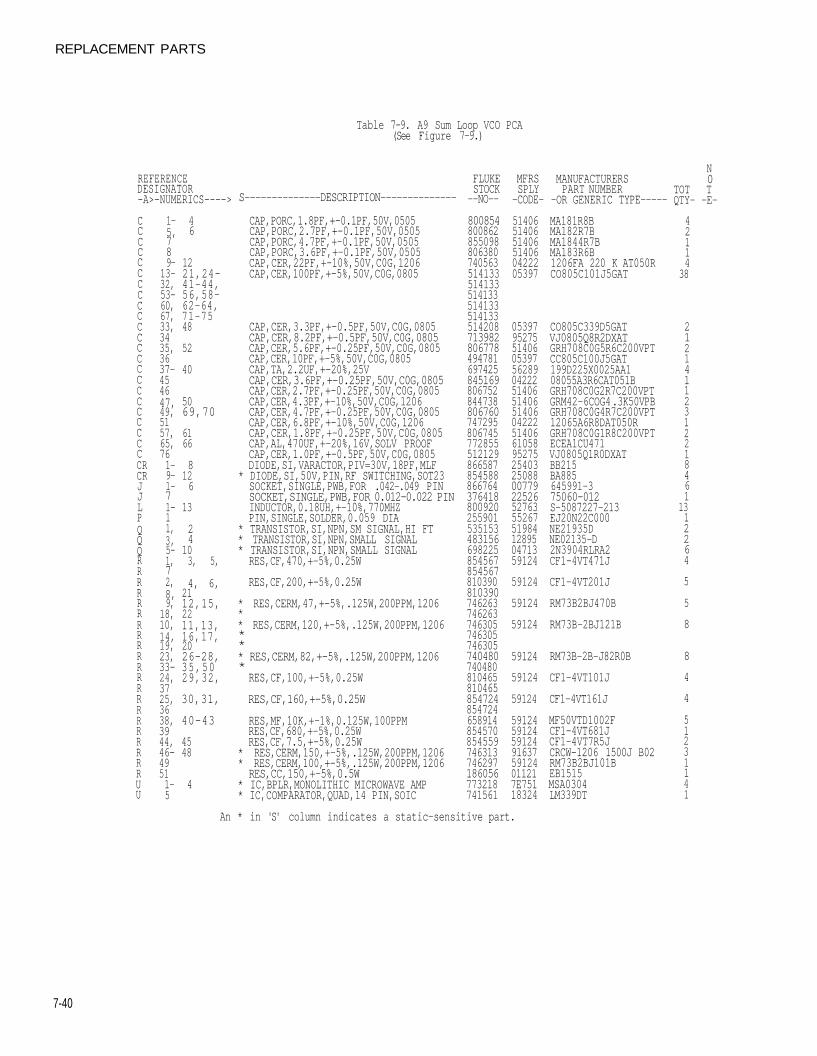
REPLACEMENT PARTS
7-40
Table 7-9. A9 Sum Loop VCO PCA(See Figure 7-9.)
REFERENCEDESIGNATOR-A>-NUMERICS---->
CCCCCCCCCCCCCCCCCCCCCCCCRCRJJLPQQQRRRRRRRRRRRRRRRRRRRRRUU
1-5,789-
13-32,53-60,67,33,3435,3637-454647,49,5157,65,761-9-1-71-11,3,5-1,72,8,9,
18,10,14,19,23,33-24,3725,3638,3944,46-49511-5
46
1221,24-41-44,56,58-62-64,71-7548
52
40
5069,70
6166
8126
13
24
103, 5,
4, 6,2112,15,2211,13,16,17,2026-28,35,5029,32,
30,31,
40-43
4548
4
S--------------DESCRIPTION--------------
CAP,PORC,1.8PF,+-0.1PF,50V,0505CAP,PORC,2.7PF,+-0.1PF,50V,0505CAP,PORC,4.7PF,+-0.1PF,50V,0505CAP,PORC,3.6PF,+-0.1PF,50V,0505CAP,CER,22PF,+-10%,50V,C0G,1206CAP,CER,100PF,+-5%,50V,C0G,0805
CAP,CER,3.3PF,+-0.5PF,50V,C0G,0805CAP,CER,8.2PF,+-0.5PF,50V,C0G,0805CAP,CER,5.6PF,+-0.25PF,50V,C0G,0805CAP,CER,10PF,+-5%,50V,C0G,0805CAP,TA,2.2UF,+-20%,25VCAP,CER,3.6PF,+-0.25PF,50V,C0G,0805CAP,CER,2.7PF,+-0.25PF,50V,C0G,0805CAP,CER,4.3PF,+-10%,50V,C0G,1206CAP,CER,4.7PF,+-0.25PF,50V,C0G,0805CAP,CER,6.8PF,+-10%,50V,C0G,1206CAP,CER,1.8PF,+-0.25PF,50V,C0G,0805CAP,AL,470UF,+-20%,16V,SOLV PROOFCAP,CER,1.0PF,+-0.5PF,50V,C0G,0805DIODE,SI,VARACTOR,PIV=30V,18PF,MLF
* DIODE,SI,50V,PIN,RF SWITCHING,SOT23SOCKET,SINGLE,PWB,FOR .042-.049 PINSOCKET,SINGLE,PWB,FOR 0.012-0.022 PININDUCTOR,0.18UH,+-10%,770MHZPIN,SINGLE,SOLDER,0.059 DIA
* TRANSISTOR,SI,NPN,SM SIGNAL,HI FT* TRANSISTOR,SI,NPN,SMALL SIGNAL* TRANSISTOR,SI,NPN,SMALL SIGNALRES,CF,470,+-5%,0.25W
RES,CF,200,+-5%,0.25W
* RES,CERM,47,+-5%,.125W,200PPM,1206** RES,CERM,120,+-5%,.125W,200PPM,1206*** RES,CERM,82,+-5%,.125W,200PPM,1206*RES,CF,100,+-5%,0.25W
RES,CF,160,+-5%,0.25W
RES,MF,10K,+-1%,0.125W,100PPMRES,CF,680,+-5%,0.25WRES,CF,7.5,+-5%,0.25W
* RES,CERM,150,+-5%,.125W,200PPM,1206* RES,CERM,100,+-5%,.125W,200PPM,1206RES,CC,150,+-5%,0.5W
* IC,BPLR,MONOLITHIC MICROWAVE AMP* IC,COMPARATOR,QUAD,14 PIN,SOIC
FLUKESTOCK--NO--
800854800862855098806380740563514133514133514133514133514133514208713982806778494781697425845169806752844738806760747295806745772855512129866587854588866764376418800920255901535153483156698225854567854567810390810390746263746263746305746305746305740480740480810465810465854724854724658914854570854559746313746297186056773218741561
MFRSSPLY-CODE-
514065140651406514060422205397
0539795275514060539756289042225140651406514060422251406610589527525403250880077922526527635526751984128950471359124
59124
59124
59124
59124
59124
59124
5912459124591249163759124011217E75118324
MANUFACTURERSPART NUMBER
-OR GENERIC TYPE-----
MA181R8BMA182R7BMA1844R7BMA183R6B1206FA 220 K AT050RCO805C101J5GAT
CO805C339D5GATVJ0805Q8R2DXATGRH708C0G5R6C200VPTCC805C100J5GAT199D225X0025AA108055A3R6CAT051BGRH708C0G2R7C200VPTGRM42-6COG4 .3K50VPBGRH708C0G4R7C200VPT12065A6R8DAT050RGRH708C0G1R8C200VPTECEA1CU471VJ0805Q1R0DXATBB215BA885645991-375060-012S-5087227-213EJ20N22C000NE21935DNE02135-D2N3904RLRA2CF1-4VT471J
CF1-4VT201J
RM73B2BJ470B
RM73B-2BJ121B
RM73B-2B-J82R0B
CF1-4VT101J
CF1-4VT161J
MF50VTD1002FCF1-4VT681JCF1-4VT7R5JCRCW-1206 1500J B02RM73B2BJ101BEB1515MSA0304LM339DT
N0
TOT TQTY- -E-
42114
38
21214112312218461
1312264
5
5
8
8
4
4
51231141
An * in 'S' column indicates a static-sensitive part.
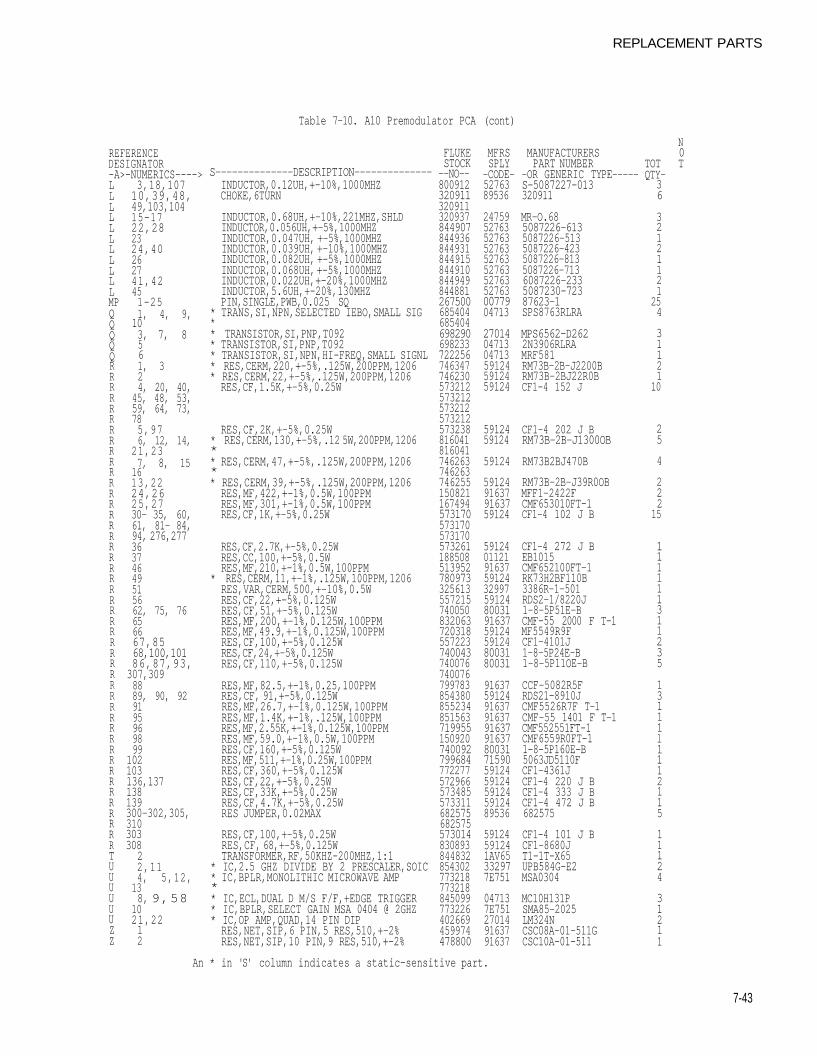
REPLACEMENT PARTS
7-43
Table 7-10. A10 Premodulator PCA (cont)
REFERENCEDESIGNATOR-A>-NUMERICS---->LLLLLLLLLLLMPQQQQQRRRRRRRRRRRRRRRRRRRRRRRRRRRRRRRRRRRRRRRRRRRRRRTUUUUUUZZ
3,18,10710,39,48,49,103,10415-1722,282324,40262741,42451-251, 4, 9,103, 7, 8561, 324, 20, 40,
45, 48, 53,59, 64, 73,785,976, 12, 14,
21,237, 8, 15
1613,2224,2625,2730- 35, 60,61, 81- 84,94, 276,27736374649515662, 75, 76656667,8568,100,10186,87,93,307,3098889, 90, 929195969899
102103136,137138139300-302,305,310303308
22,114, 5,12,
138, 9,58
1021,2212
S--------------DESCRIPTION--------------INDUCTOR,0.12UH,+-10%,1000MHZCHOKE,6TURN
INDUCTOR,0.68UH,+-10%,221MHZ,SHLDINDUCTOR,0.056UH,+-5%,1000MHZINDUCTOR,0.047UH, +-5%,1000MHZINDUCTOR,0.039UH, +-10%,1000MHZINDUCTOR,0.082UH, +-5%,1000MHZINDUCTOR,0.068UH, +-5%,1000MHZINDUCTOR,0.022UH,+-20%,1000MHZINDUCTOR,5.6UH,+-20%,130MHZPIN,SINGLE,PWB,0.025 SQ
* TRANS,SI,NPN,SELECTED IEBO,SMALL SIG** TRANSISTOR,SI,PNP,T092* TRANSISTOR,SI,PNP,T092* TRANSISTOR,SI,NPN,HI-FREQ,SMALL SIGNL* RES,CERM,220,+-5%,.125W,200PPM,1206* RES,CERM,22,+-5%,.125W,200PPM,1206RES,CF,1.5K,+-5%,0.25W
RES,CF,2K,+-5%,0.25W* RES,CERM,130,+-5%,.12 5W,200PPM,1206** RES,CERM,47,+-5%,.125W,200PPM,1206** RES,CERM,39,+-5%,.125W,200PPM,1206RES,MF,422,+-1%,0.5W,100PPMRES,MF,301,+-1%,0.5W,100PPMRES,CF,1K,+-5%,0.25W
RES,CF,2.7K,+-5%,0.25WRES,CC,100,+-5%,0.5WRES,MF,210,+-1%,0.5W,100PPM
* RES,CERM,11,+-1%,.125W,100PPM,1206RES,VAR,CERM,500,+-10%,0.5WRES,CF,22,+-5%,0.125WRES,CF,51,+-5%,0.125WRES,MF,200,+-1%,0.125W,100PPMRES,MF,49.9,+-1%,0.125W,100PPMRES,CF,100,+-5%,0.125WRES,CF,24,+-5%,0.125WRES,CF,110,+-5%,0.125W
RES,MF,82.5,+-1%,0.25,100PPMRES,CF, 91,+-5%,0.125WRES,MF,26.7,+-1%,0.125W,100PPMRES,MF,1.4K,+-1%,.125W,100PPMRES,MF,2.55K,+-1%,0.125W,100PPMRES,MF,59.0,+-1%,0.5W,100PPMRES,CF,160,+-5%,0.125WRES,MF,511,+-1%,0.25W,100PPMRES,CF,360,+-5%,0.125WRES,CF,22,+-5%,0.25WRES,CF,33K,+-5%,0.25WRES,CF,4.7K,+-5%,0.25WRES JUMPER,0.02MAX
RES,CF,100,+-5%,0.25WRES,CF, 68,+-5%,0.125WTRANSFORMER,RF,50KHZ-200MHZ,1:1
* IC,2.5 GHZ DIVIDE BY 2 PRESCALER,SOIC* IC,BPLR,MONOLITHIC MICROWAVE AMP** IC,ECL,DUAL D M/S F/F,+EDGE TRIGGER* IC,BPLR,SELECT GAIN MSA 0404 @ 2GHZ* IC,OP AMP,QUAD,14 PIN DIPRES,NET,SIP,6 PIN,5 RES,510,+-2%RES,NET,SIP,10 PIN,9 RES,510,+-2%
FLUKESTOCK--NO--800912320911320911320937844907844936844931844915844910844949844881267500685404685404698290698233722256746347746230573212573212573212573212573238816041816041746263746263746255150821167494573170573170573170573261188508513952780973325613557215740050832063720318557223740043740076740076799783854380855234851563719955150920740092799684772277572966573485573311682575682575573014830893844832854302773218773218845099773226402669459974478800
MFRSSPLY
-CODE-5276389536
24759527635276352763527635276352763527630077904713
270140471304713591245912459124
5912459124
59124
59124916379163759124
591240112191637591243299759124800319163759124591248003180031
91637591249163791637916379163780031715905912459124591245912489536
59124591241AV65332977E751
047137E751270149163791637
MANUFACTURERSPART NUMBER
-OR GENERIC TYPE-----S-5087227-013320911
MR-O.685087226-6135087226-5135087226-4235087226-8135087226-7136087226-2335087230-72387623-1SPS8763RLRA
MPS6562-D2622N3906RLRAMRF581RM73B-2B-J2200BRM73B-2BJ22R0BCF1-4 152 J
CF1-4 202 J BRM73B-2B-J1300OB
RM73B2BJ470B
RM73B-2B-J39R0OBMFF1-2422FCMF653010FT-1CF1-4 102 J B
CF1-4 272 J BEB1015CMF652100FT-1RK73H2BF110B3386R-1-501RDS2-1/8220J1-8-5P51E-BCMF-55 2000 F T-1MF5549R9FCF1-4101J1-8-5P24E-B1-8-5P11OE-B
CCF-5082R5FRDS21-8910JCMF5526R7F T-1CMF-55 1401 F T-1CMF552551FT-1CMF6559R0FT-11-8-5P160E-B5063JD5110FCF1-4361JCF1-4 220 J BCF1-4 333 J BCF1-4 472 J B682575
CF1-4 101 J BCF1-8680JT1-1T-X65UPB584G-E2MSA0304
MC10H131PSMA85-2025LM324NCSC08A-01-511GCSC10A-01-511
TOTQTY-36
32121121
254
31121
10
25
4
222
15
111111311235
13111l1112115
11124
31211
N0T
An * in 'S' column indicates a static-sensitive part.

REPLACEMENT PARTS
7-44
Table 7-l0. A10 Premodulator PCA (cont)
REFERENCEDESIGNATOR-A>-NUMERICS---->Z 3, 5
S--------------DESCRIPTION--------------RES,NET,SIP,8 PIN,4 RES,lK,+-2%
FLUKESTOCK
--NO--714345
MFRSSPLY
-CODE-80294
MANUFACTURERSPART NUMBER
-OR GENERIC TYPE-----4608H-101-102
N0
TOT TQTY- -E-
2
An * in 'S' column indicates a static-sensitive part.
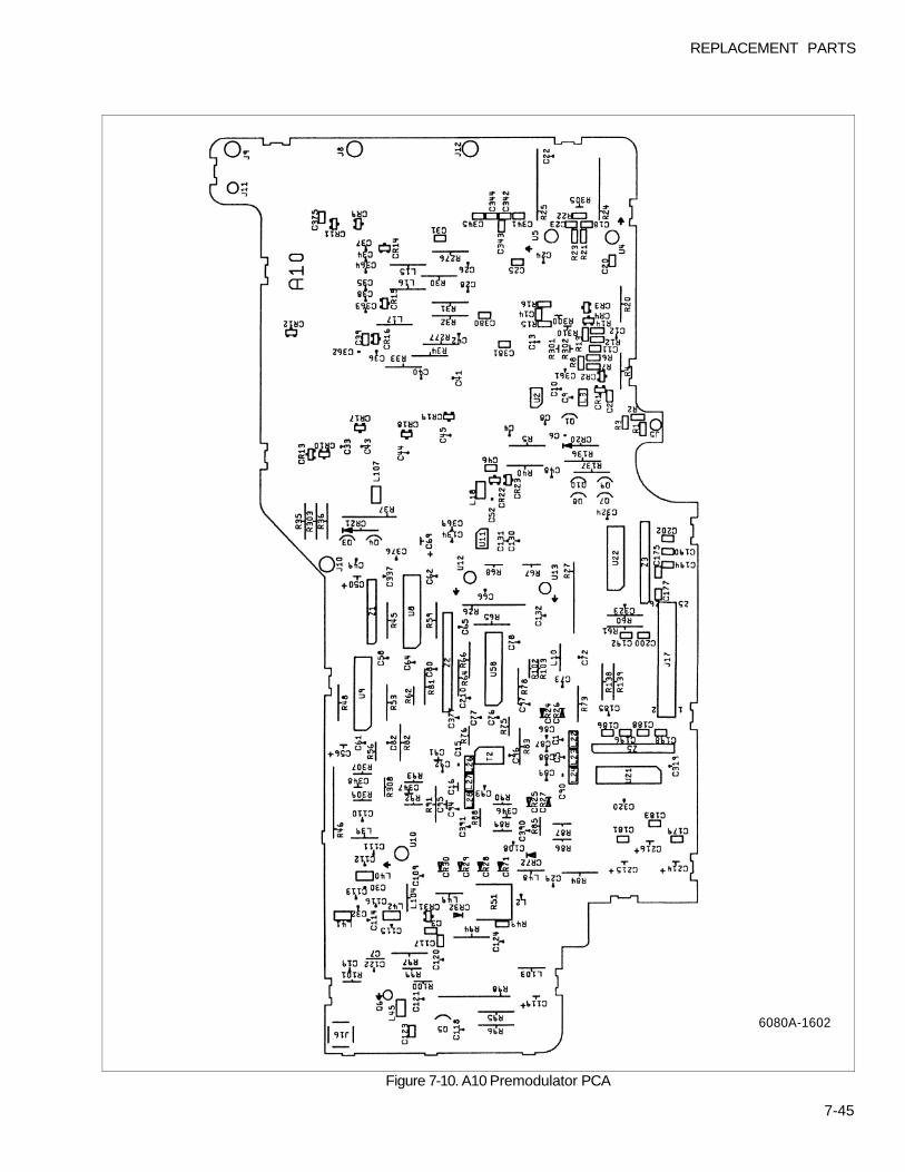
REPLACEMENT PARTS
6080A-1602
7-45
Figure 7-10. A10 Premodulator PCA
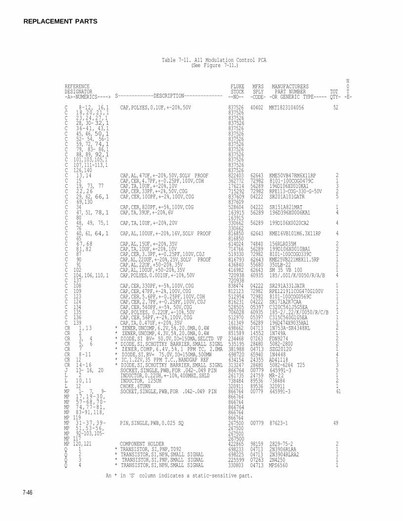
REPLACEMENT PARTS
7-46
Table 7-11. A11 Modu1ation Control PCA(See Figure 7-11.)
REFERENCEDESIGNATOR-A>-NUMERICS---->
CCCCCCCCCCCCCCCCCCCCCCCCCCCCCCCCCCCCCCCCCCCRCRCRCRCRCRCRCRJLLLMPMPMPMPMPMPMPMPMPMPMPQQQQ
8-12, 16,118,20,21,123,24,27,128, 30- 32,136-41, 43,145, 46, 50,152- 54, 56-159, 72, 74,179, 83- 86,188, 89, 92,1101,103,105,1107,111-113,1126,14013,141519, 73, 7722,2629, 62, 66,169,1303447, 51, 78,18048, 49, 75,17660, 61, 64,16567,6881,82879091
102104, 106, 110, 11371081091231241341351361391,1323, 45, 678-11
1214-1613- 16, 202
10,11121- 7, 9-17,19-30,57-68,70-74,77-81,83-9l,l18,11931-37,39-51,53-56,92-103,105-
117120,1211234
S-------------DESCRIPTION--------------
CAP,POLYES,0.1UF,+-20%,50V
CAP,AL,47UF,+-20%,50V,SOLV PROOFCAP,CER,4.7PF,+-0.25PF,100V,C0HCAP,TA,10UF,+-20%,10VCAP,CER,33PF,+-2%,50V,C0GCAP,CER,100PF,+-2%,100V,C0G
CAP,CER,820PF,+-5%,100V,C0GCAP,TA,39UF,+-20%,6V
CAP,TA,10UF,+-20%,20V
CAP,AL,100UF,+-20%,16V,SOLV PROOF
CAP,AL,15UF,+-20%,35VCAP,TA,10UF,+-20%,10VCAP,CER,3.3PF,+-0.25PF,100V,C0JCAP,AL,220UF,+-20%,25V,SOLV PROOFCAP,AL,22UF,+50-20%,35VCAP,AL,100UF,+50-20%,35VCAP,POLYES,0.001UF,+-10%,50V
CAP,CER,330PF,+-5%,100V,C0GCAP,CER,47PF,+-2%,100V,C0GCAP,CER,5.6PF,+-0.25PF,100V,C0HCAP,CER,2.7PF,+-0.25PF,100V,C0JCAP,CER,560PF,+-5%, 50V,C0GCAP,POLYES, 0.22UF,+-10%,50VCAP,CER,56PF,+-2%,100V,C0GCAP,TA,0.47UF,+-20%,35V
* ZENER,UNCOMP,6.2V,5%,20.0MA,0.4W* ZENER,UNCOMP,4.3V,5%,20.0MA,0.4W* DIODE,SI BV= 50.0V,IO=150MA,SELCTD VF* DIODE,SI,SCHOTTKY BARRIER,SMALL SIGNL* ZENER,COMP,6.4V,5%,1 PPM TC, 2.0MA* DIODE,SI,BV= 75.0V,IO=150MA,500MW* IC,1.22V,35 PPM T.C.,BANDGAP REF* DIODE,SI,SCHOTTKY BARRIER,SMALL SIGNLSOCKET,SINGLE,PWB,FOR .042-.049 PININDUCTOR,0.22UH,+-10%,400MHZ,SHLDINDUCTOR, 125UHCHOKE ,6TURNSOCKET,SINGLE,PWB,FOR .042-.049 PIN
PIN,SINGLE,PWB,0.025 SQ
COMPONENT HOLDER* TRANSISTOR, SI,PNP,T092* TRANSISTOR,SI,NPN,SMALL SIGNAL* TRANSISTOR,SI,PNP,SMALL SIGNAL* TRANSISTOR,SI,NPN,SMALL SIGNAL
FLUKESTOCK--NO--
837526837526837526837526837526837526837526837526837526837526837526837526837526822403362772176214715292837609837609528604163915163915330662330662816850816850614024714766519330816793436840416982720938720938838474812123512954816231528505706028512970161349698662851589234468535195381988698720634154313247866764261735738484320911866764866764866764866764866764866764267500267500267500267500422865698233698225225599330803
MFRSSPLY-CODE-
40402
6264372982562897298204222
0422256289
56289
62643
74840562897298262643556806264360935
042227298272982042220539760935053975628904713145520726328480047136594024355284800077924759895368953600779
00779
9815904713047130726304713
NMANUFACTURERS 0PART NUMBER TOT T
-OR GENERIC TYPE----- QTY- -E-
MKT1823104056
KME50VB47RM6X11RP8101-100COG0479C196D106X0010KA1RPE113-COG-330-G-50VSR201A101GATR
SR151A821MAT196D396X0006KA1
199D106X0020CA2
KME16VB101M6.3X11RP
156RLR035M199D106X0010BA18101-100COGO339CKME25VB221M8X11.5RP35ULB-22SM 35 VB 100185/.001/K/0050/R/A/B
SR291A331JATRRPE121911COG470G100V8101-100COG0569CSR171A2R7CAAC320C561J5G5EA185-2/.22/K/0050/R/C/BC315C560G1G5EA196D474X9035HA11N753A-SR4348RL1N749AFDN92745082-2800SZG201201N4448AD411185082-6264 T25645991-3MR- 2 2738484320911645991-3
87623-1
2829-75-22N3906RLRA2N3904RLRA22N4250MPS6560
52
21325
14
4
4
2211114
1111111121221413512161
49
21111
An * in 'S' column indicates a static-sensitive part.
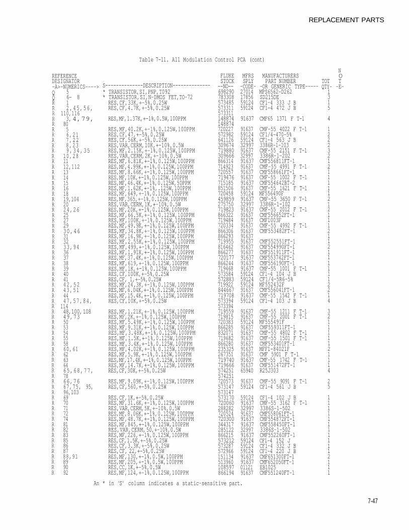
REPLACEMENT PARTS
7-47
Table 7-11. A11 Modulation Control PCA (cont)
REFERENCEDESIGNATOR-A>-NUMERICS---->QQRRRRRRRRRRRRRRRRRRRRRRRRRRRRRRRRRRRRRRRRRRRRRRRRRRRRRRRRRRRRRRRRRRRRRR
56- 812,45,56,
110,1163, 4,79,
8056,217,228,239,34,35
10,281112,112131415161819,1042024,2625272930,46313233,9436373839404142,5243,514447,57,84,
11448,100, 10849,73505354555860,6162636465,68,77,7866,7667,75, 95,96,103697071727481828385868788,91899092
S--------------DESCRIPTION--------------* TRANSISTOR,SI,PNP,T092* TRANSISTOR,SI,N-DMOS FET,TO-72RES,CF,33K,+-5%,0.25WRES,CF,4.7K,+-5%,0.25W
RES,MF,1.37K,+-1%,0.5W,100PPM
RES,MF,40.2K,+-1%,0.125W,100PPMRES,CF,47,+-5%,0.25WRES,CF,56K,+-5%,0.25WRES,VAR,CERM,10K,+-10%,0.5WRES,MF,2.15K,+-1%,0.125W,100PPMRES,VAR,CERM,2K,+-10%,0.5WRES,MF,6.81K,+-1%,0.125W,100PPMRES,MF,4.99K,+-1%,0.125W,100PPMRES,MF,8.66K,+-1%,0.125W,100PPMRES,MF,10K,+-1%,0.125W,100PPMRES,MF,46.4K,+-1%,0.125W,50PPMRES,MF,1.62K,+-1%,.125W,100PPMRES,MF,649,+-1%,0.125W,100PPMRES,MF,365,+-1%,0.125W,100PPMRES,VAR,CERM,1K,+-10%,0.5WRES,MF,20K,+-1%,0.125W,100PPMRES,MF,66.5K,+-1%,0.125W,100PPMRES,MF,100K,+-1%,0.125W,100PPMRES,MF,49.9K,+-1%,0.125W,100PPMRES,MF,34.8K,+-1%,0.125W,100PPMRES,MF,16.9K,+-1%,0.125W,100PPMRES,MF,2.55K,+-1%,0.125W,100PPMRES,MF,499,+-1%,0.125W,100PPMRES,MF,1.91K,+-1%,0.125W,100PPMRES,MF,37.4K,+-1%,0.125W,100PPMRES,MF,619,+-1%,0.125W,100PPMRES,MF,1K,+-1%,0.125W,100PPMRES,CF,100K,+-5%,0.25WRES,CF, 1,+-5%,0.25WRES,MF,24.3K,+-1%,0.125W,100PPMRES,MF,6.04K,+-1%,0.125W,100PPMRES,MF,15.4K,+-1%,0.125W,100PPMRES,CF,10K,+-5%,0.25W
RES,MF,1.21K,+-1%,0.125W,100PPMRES,MF,2K,+-1%,0.125W,100PPMRES,MF,5.49K,+-1%,0.125W,100PPMRES,MF,9.31K,+-1%,0.125W,100PPMRES,MF,3.48K,+-1%,0.125W,100PPMRES,MF,1.5K,+-1%,0.125W,100PPMRES,MF,3.4K,+-1%,0.125W,100PPMRES,MF,4.02K,+-1%,0.125W,100PPMRES,MF,5.9K,+-1%,0.125W,100PPMRES,MF,17.4K,+-1%,0.125W,100PPMRES,MF,14.7K,+-1%,0.125W,100PPMRES,CF,30K,+-5%,0.25W
RES,MF,9.09K,+-1%,0.125W,100PPMRES,CF,560,+-5%,0.25W
RES,CF,1K,+-5%,0.25WRES,MF,31.6K,+-1%,0.125W,100PPMRES,VAR,CERM,5K,+-10%,0.5WRES,MF,8.06K,+-1%,0.125W,100PPMRES,MF,48.7K,+-1%,0.125W,100PPMRES,MF,845,+-1%,0.125W,100PPMRES,VAR,CERM, 50,+-10%,0.5WRES,MF,226,+-1%,0.125W,100PPMRES,CF,1.5K,+-5%,0.25WRES,CF,3.3K,+-5%,0.25WRES,CF, 22,+-5%,0.25WRES,MF,130,+-1%,0.5W,100PPMRES,MF,205,+-1%,0.5W,100PPMRES,CC,1K,+-5%,0.5WRES,MF,124,+-1%,0.125W,100PPM
FLUKESTOCK
--NO--698290783308573485573311573311148874148874720227572982641126309674719880309666866314714923720557719476715185851506720458459859275750719823866322719484720334866306866293719955816462866277720177866244719468573584572883719922844667719708573394573394719559719815720383866285832071719682866280235325267351719740719666574251574251720573573147573147573170720060288282720524720300344317285122866215573212573287572966151134513960108597866194
MFRSSPLY
-CODE-27014178565912459124
91637
916375912459124329979163732997916379163791637916379163791637591249163732997916379163791637916379163791637916379163791637916379163791637591245912459124916379163759124
916379163759124916379163791637916379163791637916379163765940
9163759124
591249163732997916379163791637329979163759124591245912491637916370112191637
MANUFACTURERSPART NUMBER
-OR GENERIC TYPE-----MPS6562-D262SD215DECF1-4 333 J BCF1-4 472 J B
CMF65 1371 F T-1
CMF-55 4022 F T-1CF1/4-470-5%CF1-4 563 J B3386R-1-103CMF-55 2151 F T-13386R-1-202CMF556811FT-1CMF-55 4991 F T-1CMF558661FT-1CMF-55 1002 F T-1CMF554642BT-2CMF-55 1621 F T-1MF556490FCMF-55 3650 F T-13386R-1-102CMF-55 2012 F T-1CMF556652FT-1CMF1003FCMF-55 4992 F T-1CMF553482FT-1
CMF552551FT-1CMF554990FT-1CMF551911FT-1CMF553742FT-1CMF556190FT-1CMF-55 1001 F T-1CF1-4 104 J BCF1/4-5R6-5%MF552432FCMF556041FT-1CMF-55 1542 F T-1CF1-4 103 J B
CMF-55 1211 F T-1CMF-55 2001 F T-1MF555491FCMF559311FT-1CMF-55 4802 F T-1CMF-55 1501 F T-1CMF553401FT-1MFF1-84021FCMF 5901 F T-1CMF-55 1742 F T-1CMF551472FT-1R25J303
CMF-55 9091 F T-1CF1-4 561 J B
CF1-4 102 J BCMF-55 3162 F T-13386S-1-502CMF558061FT-1CMF554872FT-1CMF558450FT-13386S-1-502CMF552260FT-1CF1-4 152 JCF1-4 332 J BCF1-4 220 J BCMF651300FT-1CMF652050FT-1EB1025CMF551240FT-1
TOTQTY-1315
4
122232121111121211121121111112214
321111121114
25
111111111112111
An * in 'S' column indicates a static-sensitive part.
NOT-E-
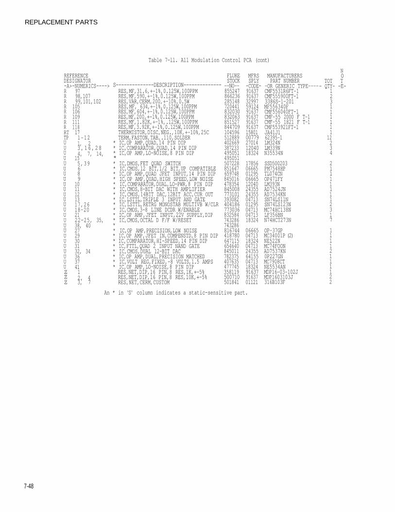
REPLACEMENT PARTS
7-48
Table 7-ll. A11 Modu1ation Control PCA (cont)
REFERENCEDESIGNATOR-A>-NUMERICS---->RRRRRRRRRTTPUUUUUUUUUUUUUUUUUUUUUUUUUZZZ
9798,10799,101,102
105106109111118171-121, 23,16,284, 7, 14,
155,39689
1011121317,2618-202122-25, 35,38, 402729303132, 3436374112, 43, 7
S--------------DESCRIPTION--------------RES,MF,31.6,+-1%,0.125W,100PPMRES,MF,590,+-1%,0.125W,100PPMRES,VAR,CERM,200,+-10%,0.5WRES,MF, 634,+-1%,0.125W,100PPMRES,MF,604,+-1%,0.125W,100PPMRES,MF,200,+-1%,0.125W,100PPMRES,MF,1.82K,+-1%,.125W,100PPMRES,MF,3.92K,+-1%,0.125W,100PPMTHERMISTOR,DISC,NEG.,10K,+-10%,25CTERM,FASTON,TAB,.110,SOLDER
* IC,OP AMP,QUAD,14 PIN DIP* IC,COMPARATOR,QUAD,14 PIN DIP* IC,OP AMP,LO-NOISE,8 PIN DIP** IC,DMOS,FET QUAD SWITCH* IC,CMOS,12 BIT,1/2 BIT,UP COMPATIBLE* IC,OP AMP,QUAD JFET INPUT,14 PIN DIP* IC,OP AMP,QUAD,HIGH SPEED,LOW NOISE* IC,COMPARATOR,DUAL,LO-PWR,8 PIN DIP* IC,CMOS,8-BIT DAC WITH AMPLIFIER* IC,CMOS,14BIT DAC,12BIT ACC,CUR OUT* IC,LSTTL,TRIPLE 3 INPUT AND GATE* IC,LSTTL,RETRG MONOSTAB MULTIVB W/CLR* IC,CMOS,3-8 LINE DCDR W/ENABLE* IC,OP AMP,JFET INPUT,22V SUPPLY,DIP* IC,CMOS,OCTAL D F/F W/RESET** IC,OP AMP,PRECISION,LOW NOISE* IC,OP AMP,JFET IN,COMPENSTD,8 PIN DIP* IC,COMPARATOR,HI-SPEED,14 PIN DIP* IC,FTTL,QUAD 2 INPUT NAND GATE* IC,CMOS,DUAL 12-BIT DAC* IC,OP AMP,DUAL,PRECISION MATCHED* IC,VOLT REG,FIXED,-8 VOLTS,1.5 AMPS* IC,OP AMP,LO-NOISE,8 PIN DIPRES,NET,DIP,16 PIN,8 RES,1K,+-5%RES,NET,DIP,16 PIN,8 RES,10K,+-5%RES,NET,CERM,CUSTOM
FLUKESTOCK
--NO--855247866236285148720441832030832063851527844709104596512889402669387233495051495051507228851647659748845016478354845008773101393082404186773036832584743286743286816744418780647115654640845011782375407635477745358119500710501841
MFRSSPLY-CODE-91637916373299759124916379163791637916371580100779270141204018324
178560666501295066651204024355243550471301295047130471318324
0666504713183240471324355641550471318324916379163701121
MANUFACTURERSPART NUMBER
-OR GENERIC TYPE----CMF5531R6FT-1CMF555900FT-13386S-1-201MF556340FCMF556040FT-1CMF-55 2000 F T-1CMF-55 1821 F T-1CMF553921FT-1JA41J162395-1LM324NLM339NN35534N
SSD500203PM7548HPTL074CNOP471FYLM393NAD7524JNAD7534KNSN74LS11NSN74LS123NMC74HC138NLF356BNN74HCT273N
OP-37GPMC34001P (2)NE522NMC74FOONAD7537KN0P227GNMC7908CTNE5534ANMDP16-03-102JMDP1603103J316B103F
N0
TOT T- QTY- -E-
123111111
12234
211111112317
11112111122
An * in 'S' column indicates a static-sensitive part.
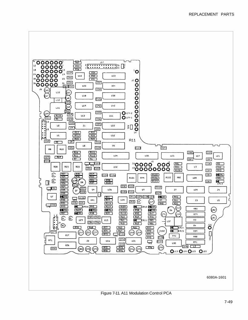
REPLACEMENT PARTS
6080A-1601
Figure 7-11. A11 Modulation Control PCA
7-49
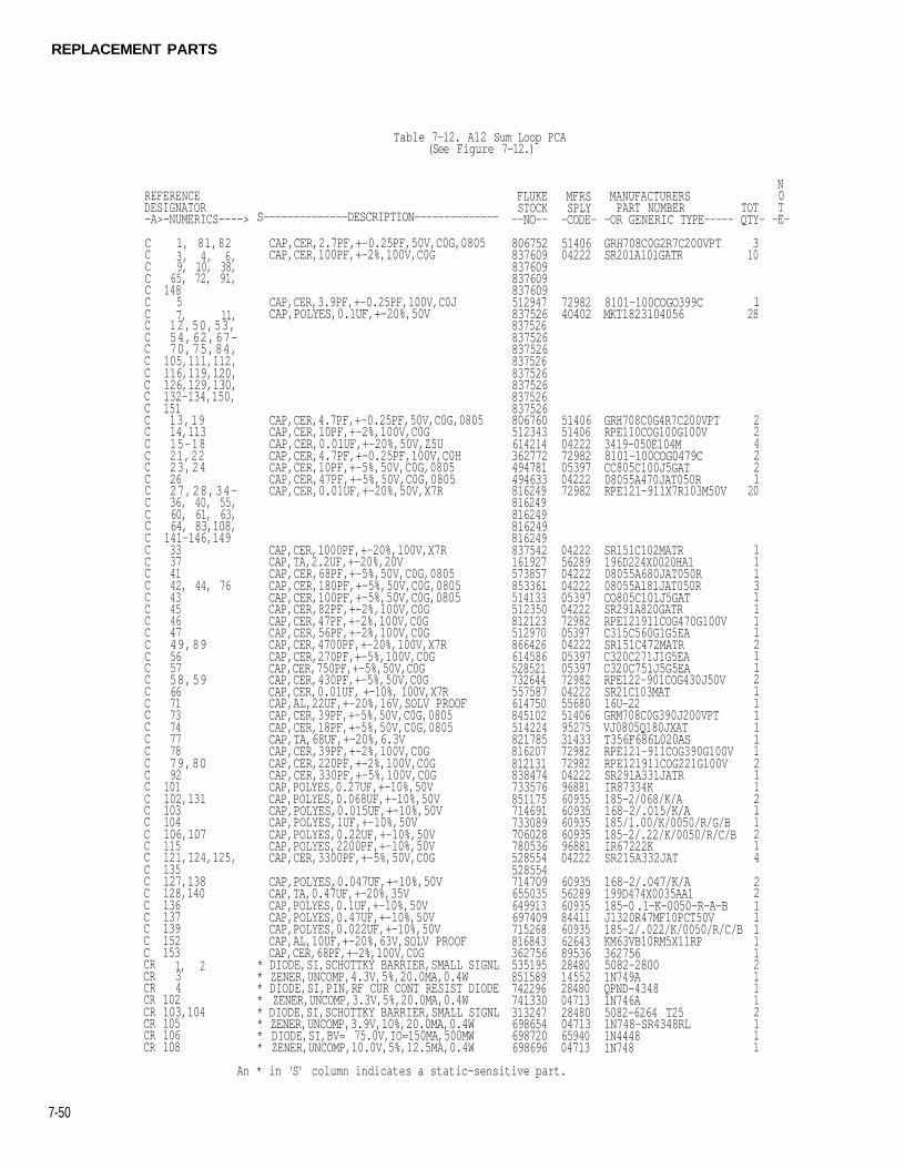
REPLACEMENT PARTS
7-50
Table 7-12. A12 Sum Loop PCA(See Figure 7-12.)
REFERENCEDESIGNATOR-A>-NUMERICS---->
CCCCCCCCCCCCCCCCCCCCCCCCCCCCCCCCCCCCCCCCCCCCCCCCCCCCCCCCCCCCCCRCRCRCRCRCRCRCR
1, 81,823, 4, 6,9, 10, 38,
65, 72, 91,148
57, 11,12,50,53,54,62,67-70,75,84,105,lll,112,116,119,120,126,129,130,
S--------------DESCRIPTION--------------
CAP,CER,2.7PF,+-0.25PF,50V,C0G,0805CAP,CER,100PF,+-2%,100V,C0G
CAP,CER,3.9PF,+-0.25PF,100V,C0JCAP,POLYES,0.1UF,+-20%,50V
132-134,150,15113,1914,11315-1821,2223,242627,28,34-36, 40, 55,60, 61, 63,64, 83,108,
CAP,CER,4.7PF,+-0.25PF,50V,C0G,0805CAP,CER,10PF,+-2%,100V,C0GCAP,CER,0.01UF,+-20%,50V,Z5UCAP,CER,4.7PF,+-0.25PF,100V,C0HCAP,CER,10PF,+-5%,50V,C0G,0805CAP,CER,47PF,+-5%,50V,C0G,0805CAP,CER,0.01UF,+-20%,50V,X7R
141-146,14933374142, 44, 764345464749,89565758,5966717374777879,8092
101102,131103104106,107115121,124,125,135127,138128,140136137139152153
1, 234
102103,104105106108
CAP,CER,1000PF,+-20%,100V,X7RCAP,TA,2.2UF,+-20%,20VCAP,CER,68PF,+-5%,50V,C0G,0805CAP,CER,180PF,+-5%,50V,C0G,0805CAP,CER,100PF,+-5%,50V,C0G,0805CAP,CER,82PF,+-2%,100V,C0GCAP,CER,47PF,+-2%,100V,C0GCAP,CER,56PF,+-2%,100V,C0GCAP,CER,4700PF,+-20%,100V,X7RCAP,CER,270PF,+-5%,100V,C0GCAP,CER,750PF,+-5%,50V,C0GCAP,CER,430PF,+-5%,50V,C0GCAP,CER,0.01UF, +-10%, 100V,X7RCAP,AL,22UF,+-20%,16V,SOLV PROOFCAP,CER,39PF,+-5%,50V,C0G,0805CAP,CER,18PF,+-5%,50V,C0G,0805CAP,TA,68UF,+-20%,6.3VCAP,CER,39PF,+-2%,100V,C0GCAP,CER,220PF,+-2%,100V,C0GCAP,CER,330PF,+-5%,100V,C0GCAP,POLYES,0.27UF,+-10%,50VCAP,POLYES,0.068UF,+-10%,50VCAP,POLYES,0.015UF,+-10%,50VCAP,POLYES,1UF,+-10%,50VCAP,POLYES,0.22UF,+-10%,50VCAP,POLYES,2200PF,+-10%,50VCAP,CER,3300PF,+-5%,50V,C0G
CAP,POLYES,0.047UF,+-10%,50VCAP,TA,0.47UF,+-20%,35VCAP,POLYES,0.1UF,+-10%,50VCAP,POLYES,0.47UF,+-10%,50VCAP,POLYES,0.022UF,+-10%,50VCAP,AL,10UF,+-20%,63V,SOLV PROOFCAP,CER,68PF,+-2%,100V,C0G
* DIODE,SI,SCHOTTKY BARRIER,SMALL SIGNL* ZENER,UNCOMP,4.3V,5%,20.0MA,0.4W* DIODE,SI,PIN,RF CUR CONT RESIST DIODE* ZENER,UNCOMP,3.3V,5%,20.0MA,0.4W* DIODE,SI,SCHOTTKY BARRIER,SMALL SIGNL* ZENER,UNCOMP,3.9V,10%,20.0MA,0.4W* DIODE,SI,BV= 75.0V,IO=150MA,500MW* ZENER,UNCOMP,10.0V,5%,12.5MA,0.4W
FLUKESTOCK--NO--
806752837609837609837609837609512947837526837526837526837526837526837526837526837526837526806760512343614214362772494781494633816249816249816249816249816249837542161927573857853361514133512350812123512970866426614586528521732644557587614750845102514224821785816207812131838474733576851175714691733089706028780536528554528554714709655035649913697409715268816843362756535195851589742296741330313247698654698720698696
MFRSSPLY-CODE-
5140604222
7298240402
51406514060422272982053970422272982
042225628904222042220539704222729820539704222053970539772982042225568051406952753143372982729820422296881609356093560935609359688104222
609355628960935844116093562643895362848014552284800471328480047136594004713
MANUFACTURERSPART NUMBER TOT
-OR GENERIC TYPE----- QTY-
GRH708C0G2R7C200VPT 3SR201A101GATR
8101-100COGO399CMKT1823104056
GRH708C0G4R7C200VPTRPE110COG100G100V3419-050E104M8101-100COG0479CCC805C100J5GAT08055A470JAT050RRPE121-911X7R103M50V
SR151C102MATR196D224X0020HA108055A680JAT050R08055A181JAT050RCO805C101J5GATSR291A820GATRRPE121911COG470G100VC315C560G1G5EASR151C472MATRC320C271J1G5EAC320C751J5G5EARPE122-901COG430J50VSR21C103MAT16U-22GRM708C0G390J200VPTVJ0805Q180JXATT356F686L020ASRPE121-911COG390G100VRPE121911COG221G100VSR291A331JATRIR87334K185-2/068/K/A168-2/.015/K/A185/1.00/K/0050/R/G/B185-2/.22/K/0050/R/C/BIR67222KSR215A332JAT
168-2/.047/K/A199D474X0035AA1185-0 .1-K-0050-R-A-BJ1320R47MF10PCT50V185-2/.022/K/0050/R/C/BKM63VB10RM5X11RP3627565082-28001N749AQPND-43481N746A5082-6264 T251N748-SR4348RL1N44481N748
10
128
22422120
111311112112111111211211214
221111121112111
N0T-E-
An * in 'S' column indicates a static-sensitive part.
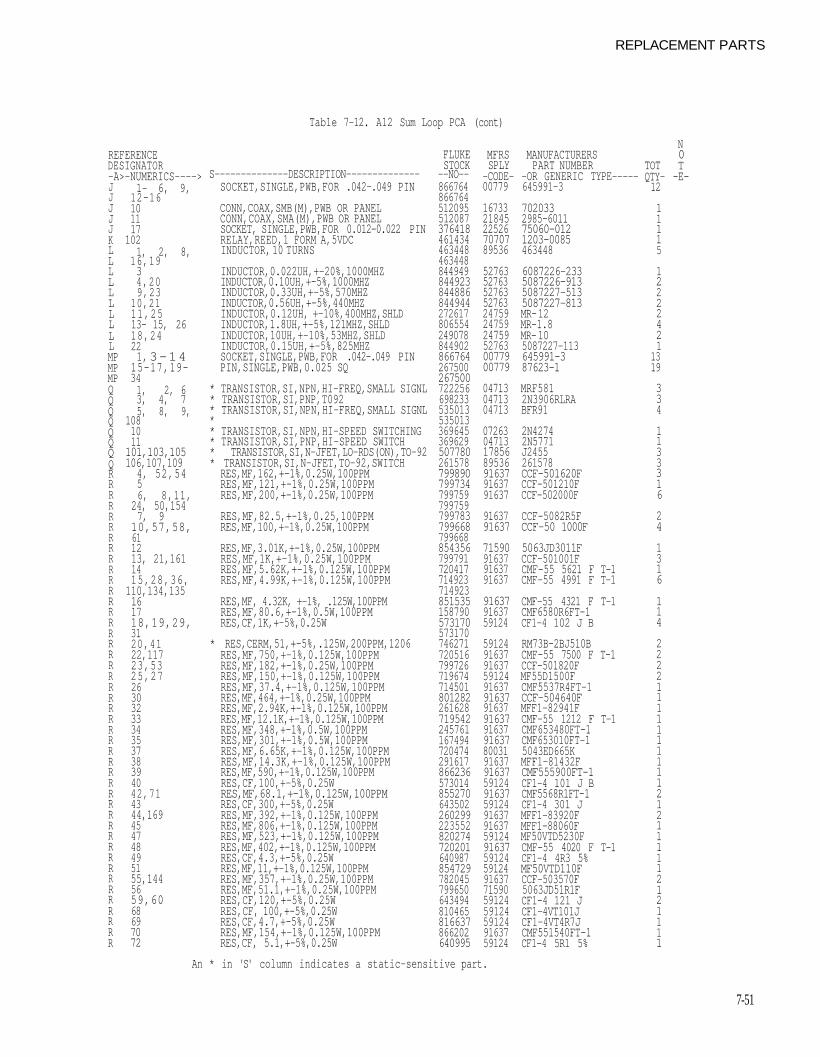
REPLACEMENT PARTS
7-51
Tab1e 7-12. A12 Sum Loop PCA (cont)
REFERENCEDESIGNATOR-A>-NUMERICS---->JJJJJKLLLLLLLLLLMPMPMPQQQQQQQQRRRRRRRRRRRRRRRRRRRRRRRRRRRRRRRRRRRRRRRRRRRRR
1- 6, 9,12-16101117102
1, 2, 8,16,1934,209,23
10,2111,2513- 15, 2618,24221, 3-14
15-17,19-341, 2, 63, 4, 75, 8, 9,
1081011101,103,105106,107,109
4, 52,5456, 8,11,
24, 50,1547, 910,57,58,611213, 21,1611415,28,36,110,134,135161718,19,29,3120,4122,11723,5325,272630323334353738394042,714344,169454748495155,1445659,6068697072
S--------------DESCRIPTION--------------SOCKET,SINGLE,PWB,FOR .042-.049 PIN
CONN,COAX,SMB(M),PWB OR PANELCONN,COAX,SMA(M),PWB OR PANELSOCKET, SINGLE,PWB,FOR 0.012-0.022 PINRELAY,REED,1 FORM A,5VDCINDUCTOR, 10 TURNS
INDUCTOR,0.022UH,+-20%,1000MHZINDUCTOR,0.10UH,+-5%,1000MHZINDUCTOR,0.33UH,+-5%,570MHZINDUCTOR,0.56UH,+-5%,440MHZINDUCTOR,0.12UH, +-10%,400MHZ,SHLDINDUCTOR,1.8UH,+-5%,121MHZ,SHLDINDUCTOR,10UH,+-10%,53MHZ,SHLDINDUCTOR,0.15UH,+-5%,825MHZSOCKET,SINGLE,PWB,FOR .042-.049 PINPIN,SINGLE,PWB,0.025 SQ
* TRANSISTOR,SI,NPN,HI-FREQ,SMALL SIGNL* TRANSISTOR,SI,PNP,T092* TRANSISTOR,SI,NPN,HI-FREQ,SMALL SIGNL** TRANSISTOR,SI,NPN,HI-SPEED SWITCHING* TRANSISTOR,SI,PNP,HI-SPEED SWITCH* TRANSISTOR,SI,N-JFET,LO-RDS(ON),TO-92* TRANSISTOR,SI,N-JFET,TO-92,SWITCHRES,MF,162,+-1%,0.25W,100PPMRES,MF,121,+-1%,0.25W,100PPMRES,MF,200,+-1%,0.25W,100PPM
RES,MF,82.5,+-1%,0.25,100PPMRES,MF,100,+-1%,0.25W,100PPM
RES,MF,3.01K,+-1%,0.25W,100PPMRES,MF,1K,+-1%,0.25W,100PPMRES,MF,5.62K,+-1%,0.125W,100PPMRES,MF,4.99K,+-1%,0.125W,100PPM
RES,MF, 4.32K, +-1%, .125W,100PPMRES,MF,80.6,+-1%,0.5W,100PPMRES,CF,1K,+-5%,0.25W
* RES,CERM,51,+-5%,.125W,200PPM,1206RES,MF,750,+-1%,0.125W,100PPMRES,MF,182,+-1%,0.25W,100PPMRES,MF,150,+-1%,0.125W,100PPMRES,MF,37.4,+-1%,0.125W,100PPMRES,MF,464,+-1%,0.25W,100PPMRES,MF,2.94K,+-1%,0.125W,100PPMRES,MF,12.1K,+-1%,0.125W,100PPMRES,MF,348,+-1%,0.5W,100PPMRES,MF,301,+-1%,0.5W,100PPMRES,MF,6.65K,+-1%,0.125W,100PPMRES,MF,14.3K,+-1%,0.125W,100PPMRES,MF,590,+-1%,0.125W,100PPMRES,CF,100,+-5%,0.25WRES,MF,68.1,+-1%,0.125W,100PPMRES,CF,300,+-5%,0.25WRES,MF,392,+-1%,0.125W,100PPMRES,MF,806,+-1%,0.125W,100PPMRES,MF,523,+-1%,0.125W,100PPMRES,MF,402,+-1%,0.125W,100PPMRES,CF,4.3,+-5%,0.25WRES,MF,11,+-1%,0.125W,100PPMRES,MF,357,+-1%,0.25W,100PPMRES,MF,51.1,+-1%,0.25W,100PPMRES,CF,120,+-5%,0.25WRES,CF, 100,+-5%,0.25WRES,CF,4.7,+-5%,0.25WRES,MF,154,+-1%,0.125W,100PPMRES,CF, 5.1,+-5%,0.25W
FLUKESTOCK--NO--866764866764512095512087376418461434463448463448844949844923844886844944272617806554249078844902866764267500267500722256698233535013535013369645369629507780261578799890799734799759799759799783799668799668854356799791720417714923714923851535158790573170573170746271720516799726719674714501801282261628719542245761167494720474291617866236573014855270643502260299223552820274720201640987854729782045799650643494810465816637866202640995
MFRSSPLY
-CODE-00779
1673321845225267070789536
52763527635276352763247592475924759527630077900779
047130471304713
07263047131785689536916379163791637
9163791637
71590916379163791637
916379163759124
5912491637916375912491637916379163791637916379163780031916379163759124916375912491637916375912491637591245912491637715905912459124591249163759124
MANUFACTURERSPART NUMBER
-OR GENERIC TYPE-----645991-3
7020332985-601175060-0121203-0085463448
6087226-2335087226-9135087227-5135087227-813MR- 12MR-1.8MR- 105087227-113645991-387623-1
MRF5812N3906RLRABFR91
2N42742N5771J2455261578CCF-501620FCCF-501210FCCF-502000F
CCF-5082R5FCCF-50 1000F
5063JD3011FCCF-501001FCMF-55 5621 F T-1CMF-55 4991 F T-1
CMF-55 4321 F T-1CMF6580R6FT-1CF1-4 102 J B
RM73B-2BJ510BCMF-55 7500 F T-1CCF-501820FMF55D1500FCMF5537R4FT-1CCF-504640FMFF1-82941FCMF-55 1212 F T-1CMF653480FT-1CMF653010FT-15043ED665KMFF1-81432FCMF555900FT-1CF1-4 101 J BCMF5568R1FT-1CF1-4 301 JMFF1-83920FMFF1-88060FMF50VTD5230FCMF-55 4020 F T-1CF1-4 4R3 5%MF50VTD110FCCF-503570F5063JD51R1FCF1-4 121 JCF1-4VT101JCF1-4VT4R7JCMF551540FT-1CF1-4 5R1 5%
TOTQTY-12
11115
12222421
1319
334
1133316
24
1316
114
22221111111111212111112121111
N0T-E-
An * in 'S' column indicates a static-sensitive part.
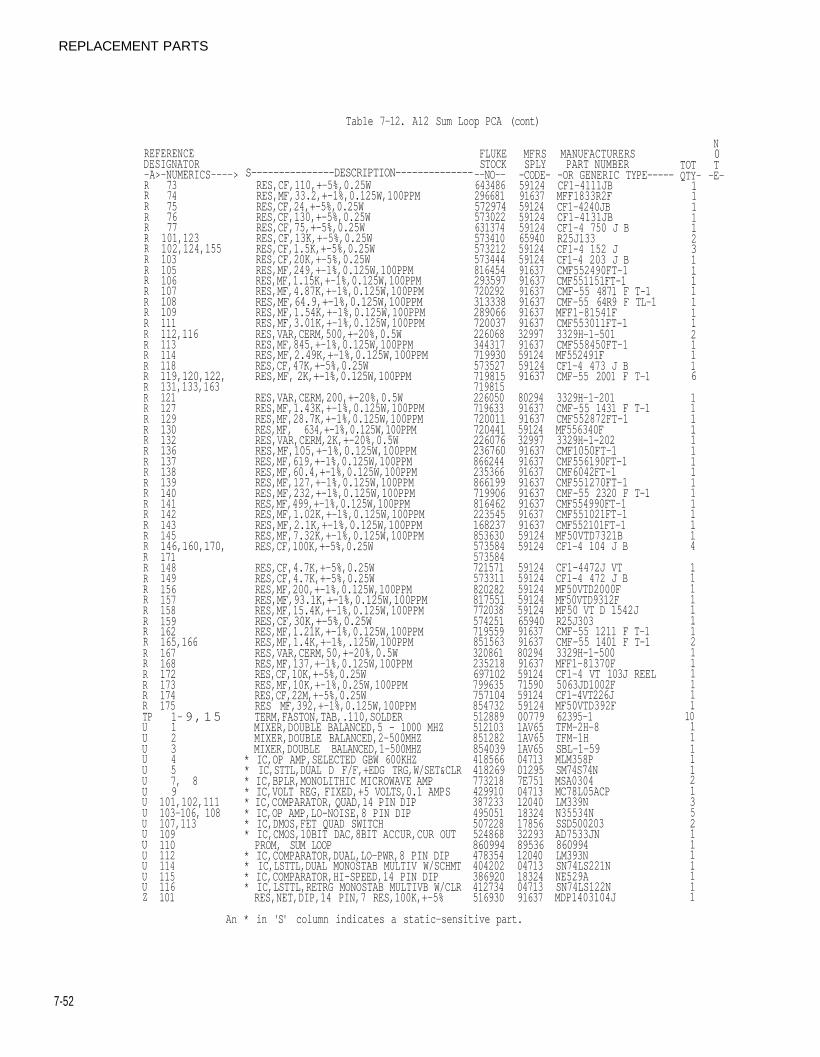
REPLACEMENT PARTS
7-52
Tab1e 7-12. A12 Sum Loop PCA (cont)
REFERENCEDESIGNATOR-A>-NUMERICS---->RRRRRRRRRRRRRRRRRRRRRRRRRRRRRRRRRRRRRRRRRRRRRRRRRRTPUUUUUUUUUUUUUUUUZ
7374757677101,123102,124,155103105106107108109111112,116113114118119,120,122,131,133,163121127129130132136137138139140141142143145146,160,170,171148149156157158159162165,1661671681721731741751- 9,15123457, 89
101,102,111103-106, 108107,113109110112114115116101
An
S---------------DESCRIPTION--------------RES,CF,110,+-5%,0.25WRES,MF,33.2,+-1%,0.125W,100PPMRES,CF,24,+-5%,0.25WRES,CF,130,+-5%,0.25WRES,CF,75,+-5%,0.25WRES,CF,13K,+-5%,0.25WRES,CF,1.5K,+-5%,0.25WRES,CF,20K,+-5%,0.25WRES,MF,249,+-1%,0.125W,100PPMRES,MF,1.15K,+-1%,0.125W,100PPMRES,MF,4.87K,+-1%,0.125W,100PPMRES,MF,64.9,+-1%,0.125W,100PPMRES,MF,1.54K,+-1%,0.125W,100PPMRES,MF,3.01K,+-1%,0.125W,100PPMRES,VAR,CERM,500,+-20%,0.5WRES,MF,845,+-1%,0.125W,100PPMRES,MF,2.49K,+-1%,0.125W,100PPMRES,CF,47K,+-5%,0.25WRES,MF, 2K,+-1%,0.125W,100PPM
RES,VAR,CERM,200,+-20%,0.5WRES,MF,1.43K,+-1%,0.125W,100PPMRES,MF,28.7K,+-1%,0.125W,100PPMRES,MF, 634,+-1%,0.125W,100PPMRES,VAR,CERM,2K,+-20%,0.5WRES,MF,105,+-1%,0.125W,100PPMRES,MF,619,+-1%,0.125W,100PPMRES,MF,60.4,+-1%,0.125W,100PPMRES,MF,127,+-1%,0.125W,100PPMRES,MF,232,+-1%,0.125W,100PPMRES,MF,499,+-1%,0.125W,100PPMRES,MF,1.02K,+-1%,0.125W,100PPMRES,MF,2.1K,+-1%,0.125W,100PPMRES,MF,7.32K,+-1%,0.125W,100PPMRES,CF,100K,+-5%,0.25W
RES,CF,4.7K,+-5%,0.25WRES,CF,4.7K,+-5%,0.25WRES,MF,200,+-1%,0.125W,100PPMRES,MF,93.1K,+-1%,0.125W,100PPMRES,MF,15.4K,+-1%,0.125W,100PPMRES,CF,30K,+-5%,0.25WRES,MF,1.21K,+-1%,0.125W,100PPMRES,MF,1.4K,+-1%,.125W,100PPMRES,VAR,CERM,50,+-20%,0.5WRES,MF,137,+-1%,0.125W,100PPMRES,CF,10K,+-5%,0.25WRES,MF,10K,+-1%,0.25W,100PPMRES,CF,22M,+-5%,0.25WRES MF,392,+-1%,0.125W,100PPMTERM,FASTON,TAB,.110,SOLDERMIXER,DOUBLE BALANCED,5 - 1000 MHZMIXER,DOUBLE BALANCED,2-500MHZMIXER,DOUBLE BALANCED,1-500MHZ
* IC,OP AMP,SELECTED GBW 600KHZ* IC,STTL,DUAL D F/F,+EDG TRG,W/SET&CLR* IC,BPLR,MONOLITHIC MICROWAVE AMP* IC,VOLT REG, FIXED,+5 VOLTS,0.1 AMPS* IC,COMPARATOR, QUAD,14 PIN DIP* IC,OP AMP,LO-NOISE,8 PIN DIP* IC,DMOS,FET QUAD SWITCH* IC,CMOS,10BIT DAC,8BIT ACCUR,CUR OUTPROM, SUM LOOP
* IC,COMPARATOR,DUAL,LO-PWR,8 PIN DIP* IC,LSTTL,DUAL MONOSTAB MULTIV W/SCHMT* IC,COMPARATOR,HI-SPEED,14 PIN DIP* IC,LSTTL,RETRG MONOSTAB MULTIVB W/CLRRES,NET,DIP,14 PIN,7 RES,100K,+-5%
FLUKESTOCK--NO--643486296681572974573022631374573410573212573444816454293597720292313338289066720037226068344317719930573527719815719815226050719633720011720441226076236760866244235366866199719906816462223545168237853630573584573584721571573311820282817551772038574251719559851563320861235218697102799635757104854732512889512103851282854039418566418269773218429910387233495051507228524868860994478354404202386920412734516930
MFRS MANUFACTURERSSPLY PART NUMBER-CODE- -OR GENERIC TYPE-----59124 CF1-4111JB916375912459124591246594059124591249163791637916379163791637916373299791637591245912491637
802949163791637591243299791637916379163791637916379163791637916375912459124
5912459124591245912459124659409163791637802949163759124715905912459124007791AV651AV651AV6504713012957E7510471312040183241785632293895361204004713183240471391637
MFF1833R2FCF1-4240JBCF1-4131JBCF1-4 750 J BR25J133CF1-4 152 JCF1-4 203 J BCMF552490FT-1CMF551151FT-1CMF-55 4871 F T-1CMF-55 64R9 F TL-1MFF1-81541FCMF553011FT-13329H-1-501CMF558450FT-1MF552491FCF1-4 473 J BCMF-55 2001 F T-1
3329H-1-201CMF-55 1431 F T-1CMF552872FT-1MF556340F3329H-1-202CMF1050FT-1CMF556190FT-1CMF6042FT-1CMF551270FT-1CMF-55 2320 F T-1CMF554990FT-1CMF551021FT-1CMF552101FT-1MF50VTD7321BCF1-4 104 J B
CF1-4472J VTCF1-4 472 J BMF50VTD2000FMF50VTD9312FMF50 VT D 1542JR25J303CMF-55 1211 F T-1CMF-55 1401 F T-13329H-1-500MFF1-81370FCF1-4 VT 103J REEL5063JD1002FCF1-4VT226JMF50VTD392F62395-1TFM-2H-8TFM-1HSBL-1-59MLM358PSM74S74NMSA0304MC78L05ACPLM339NN35534NSSD500203AD7533JN860994LM393NSN74LS221NNE529ASN74LS122NMDP1403104J
TOTQTY-1111123111111121116
111111111111114
111111121111111011111213521111111
* in 'S' column indicates a static-sensitive part.
N0T-E-
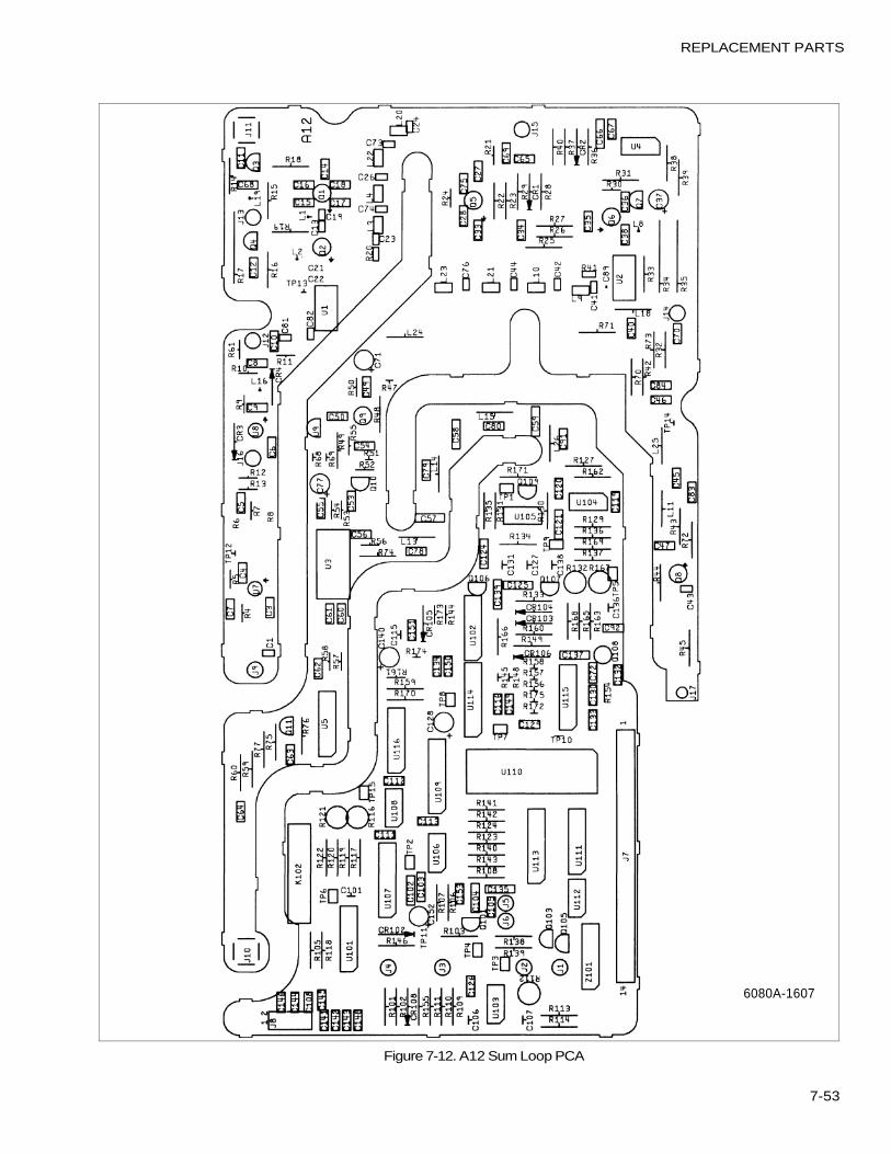
REPLACEMENT PARTS
Figure 7-12. A12 Sum Loop PCA
7-53
6080A-1607
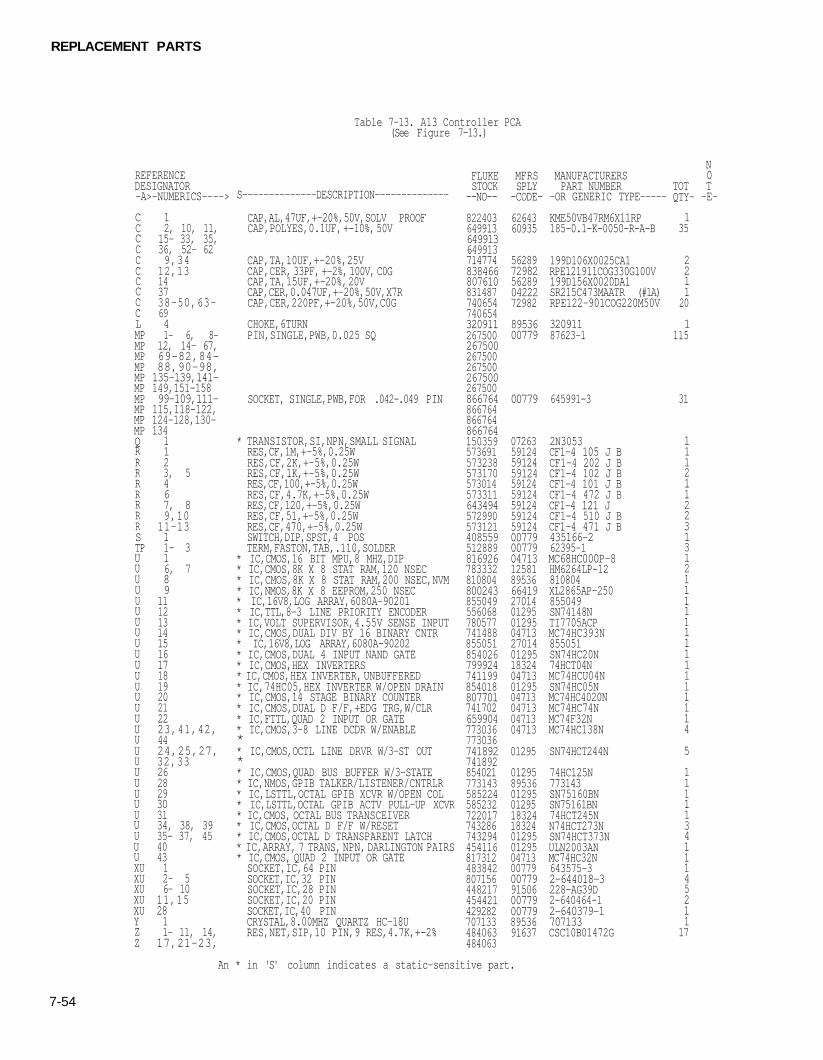
REPLACEMENT PARTS
7-54
Table 7-13. A13 Controller PCA(See Figure 7-13.)
REFERENCEDESIGNATOR-A>-NUMERICS---->
CCCCCCCCCCLMPMPMPMPMPMPMPMPMPMPQRRRRRRRRSTPUUUUUUUUUUUUUUUUUUUUUUUUUUUUUXUXUXUXUXUYZZ
12, 10, 11,
15- 33, 35,36, 52- 629,34
12,13143738-50,63-6941- 6, 8-
12, 14- 67,69-82,84-88,90-98,135-139,141-149,151-15899-109,111-115,118-122,124-128,130-1341123, 5467, 89,10
11-1311- 316, 789
11121314151617181920212223,41,42,4424,25,27,32,33262829303134, 38, 3935- 37, 45404312- 56- 10
11,152811- 11, 14,17,21-23,
S--------------DESCRIPTION--------------
CAP,AL,47UF,+-20%,50V,SOLV PROOFCAP,POLYES,0.1UF, +-10%, 50V
CAP,TA,10UF,+-20%,25VCAP,CER, 33PF, +-2%, 100V, C0GCAP,TA,15UF,+-20%, 20VCAP,CER,0.047UF,+-20%,50V,X7RCAP,CER,220PF,+-20%,50V,C0G
CHOKE,6TURNPIN,SINGLE,PWB,0.025 SQ
SOCKET, SINGLE,PWB,FOR .042-.049 PIN
* TRANSISTOR,SI,NPN,SMALL SIGNALRES,CF,1M,+-5%,0.25WRES,CF,2K,+-5%,0.25WRES,CF,1K,+-5%,0.25WRES,CF,100,+-5%,0.25WRES,CF,4.7K,+-5%,0.25WRES,CF,120,+-5%,0.25WRES,CF,51,+-5%,0.25WRES,CF,470,+-5%,0.25WSWITCH,DIP,SPST,4 POSTERM,FASTON,TAB,.110,SOLDER
* IC,CMOS,16 BIT MPU,8 MHZ,DIP* IC,CMOS,8K X 8 STAT RAM,120 NSEC* IC,CMOS,8K X 8 STAT RAM,200 NSEC,NVM* IC,NMOS,8K X 8 EEPROM,250 NSEC* IC,16V8,LOG ARRAY,6080A-90201* IC,TTL,8-3 LINE PRIORITY ENCODER* IC,VOLT SUPERVISOR,4.55V SENSE INPUT* IC,CMOS,DUAL DIV BY 16 BINARY CNTR* IC,16V8,LOG ARRAY,6080A-90202* IC,CMOS,DUAL 4 INPUT NAND GATE* IC,CMOS,HEX INVERTERS* IC,CMOS,HEX INVERTER, UNBUFFERED* IC,74HC05,HEX INVERTER W/OPEN DRAIN* IC,CMOS,14 STAGE BINARY COUNTER* IC,CMOS,DUAL D F/F,+EDG TRG,W/CLR* IC,FTTL,QUAD 2 INPUT OR GATE* IC,CMOS,3-8 LINE DCDR W/ENABLE** IC,CMOS,OCTL LINE DRVR W/3-ST OUT** IC,CMOS,QUAD BUS BUFFER W/3-STATE* IC,NMOS,GPIB TALKER/LISTENER/CNTRLR* IC,LSTTL,OCTAL GPIB XCVR W/OPEN COL* IC,LSTTL,OCTAL GPIB ACTV PULL-UP XCVR* IC,CMOS, OCTAL BUS TRANSCEIVER* IC,CMOS,OCTAL D F/F W/RESET* IC,CMOS,OCTAL D TRANSPARENT LATCH* IC,ARRAY, 7 TRANS, NPN, DARLINGTON PAIRS* IC,CMOS, QUAD 2 INPUT OR GATESOCKET,IC,64 PINSOCKET,IC,32 PINSOCKET,IC,28 PINSOCKET,IC,20 PINSOCKET,IC,40 PINCRYSTAL,8.00MHZ QUARTZ HC-18URES,NET,SIP,10 PIN,9 RES,4.7K,+-2%
FLUKESTOCK--NO--
822403649913649913649913714774838466807610831487740654740654320911267500267500267500267500267500267500866764866764866764866764150359573691573238573170573014573311643494572990573121408559512889816926783332810804800243855049556068780577741488855051854026799924741199854018807701741702659904773036773036741892741892854021773143585224585232722017743286743294454116817312483842807156448217454421429282707133484063484063
MFRSSPLY-CODE-
6264360935
5628972982562890422272982
8953600779
00779
07263591245912459124591245912459124591245912400779007790471312581895366641927014012950129504713270140129518324047130129504713047130471304713
01295
01295895360129501295183241832401295012950471300779007799150600779007798953691637
MANUFACTURERSPART NUMBER
-OR GENERIC TYPE-----
KME50VB47RM6X11RP185-0.1-K-0050-R-A-B
199D106X0025CA1RPE121911COG330G100V199D156X0020DA1SR215C473MAATR (#1A)RPE122-901COG220M50V
32091187623-1
645991-3
2N3053CF1-4 105 J BCF1-4 202 J BCF1-4 102 J BCF1-4 101 J BCF1-4 472 J BCF1-4 121 JCF1-4 510 J BCF1-4 471 J B435166-262395-1MC68HC000P-8HM6264LP-12810804XL2865AP-250855049SN74148NTI7705ACPMC74HC393N855051SN74HC20N74HCT04NMC74HCU04NSN74HC05NMC74HC4020NMC74HC74NMC74F32NMC74HC138N
SN74HCT244N
74HC125N773143SN75160BNSN75161BN74HCT245NN74HCT273NSN74HCT373NULN2003ANMC74HC32N643575-32-644018-3228-AG39D2-640464-12-640379-1707133CSC10B01472G
TOTQTY-
135
221120
1115
31
1112112231312111111111111114
5
11111341114521117
N0T-E-
An * in 'S' column indicates a static-sensitive part.

REPLACEMENT PARTS
7-55
Table 7-13. A13 Contro11er PCA (cont)
REFERENCEDESIGNATOR-A>-NUMERICS---->ZZZ
2512,16,1920,24
S--------------DESCRIPTION--------------
RES,NET,SIP,6 PIN,5 RES,4.7K,+-2%RES,NET,DIP,16 PIN,8 RES,120,+-5%
FLUKESTOCK
--NO--484063494690448423
MFRSSPLY
-CODE-
9163791637
MANUFACTURERSPART NUMBER
-OR GENERIC TYPE-----
CSC06B01472GMDP16-03-121J
TOTQTY-
32
N0T-E-
An * in 'S' column indicates a static-sensitive part.
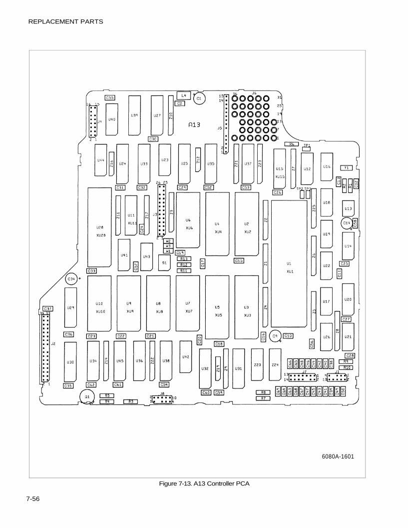
REPLACEMENT PARTS
7-56
Figure 7-13. A13 Controller PCA
6080A-1601
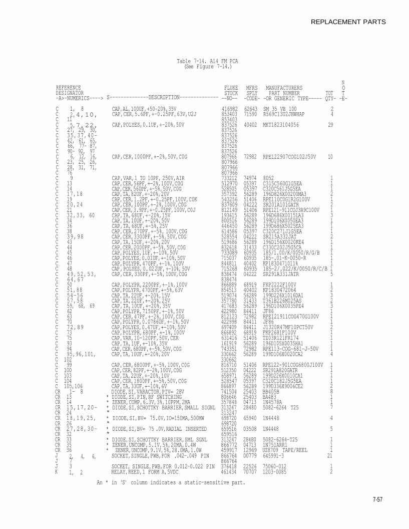
REPLACEMENT PARTS
7-57
Tab1e 7-14. A14 FM PCA(See Figure 7-14.)
REFERENCEDESIGNATOR-A>-NUMERICS---->
CCCCCCCCCCCCCCCCCCCCCCCCCCCCCCCCCCCCCCCCCCCCCCCCCCCCCCRCRCRCRCRCRCRCRCRCRCRCRJJJK
1, 82, 4,10,
115, 7,22,27, 29, 30,35,37,40-42, 61, 65,66, 77- 87,90- 92, 976, 12, 16,
23, 25, 26,28, 31, 71,769
131417,181920,242132,33, 6034363839,9843444546474849,52,53,64,675051,8854-5657,5859, 68, 6962637072,897375939495,96,101,
10299
100103104105,1061- 8
131415,17,20-2418,19,25,2627,28,30-323335362, 4, 6,731, 2
S--------------DESCRIPTION--------------
CAP,AL,100UF,+50-20%,35VCAP,CER,5.6PF,+-0.25PF,63V,U2J
CAP,POLYES,0.1UF,+-20%,50V
CAP,CER,1000PF,+-2%,50V,C0G
CAP,VAR,1 TO 10PF, 250V,AIRCAP,CER,56PF,+-2%,100V,C0GCAP,CER,560PF,+-5%,50V,C0GCAP,TA,82UF,+-20%,20VCAP,CER,1.2PF,+-0.25PF,100V,C0KCAP,CER,100PF,+-2%,100V,C0GCAP,CER,3.9PF,+-0.25PF,100V,C0JCAP,TA,68UF,+-20%,15VCAP,TA,10UF,+-20%,50VCAP,TA,68UF,+-5%,25VCAP,CER,270PF,+-5%, 100V,C0GCAP,CER,3300PF,+-5%,50V,C0GCAP,TA,15UF,+-20%,20VCAP,CER,2000PF,+-5%,50V,C0GCAP,POLYES,1UF,+-10%,50VCAP,POLYES,0.01UF,+-10%,50VCAP,POLYPR,470PF,+-1%,100VCAP , POLYES, 0. 02 2UF, +-10%, 50VCAP,CER,330PF,+-5%, 100V,C0G
CAP,POLYPR,2200PF,+-1%,100VCAP,POLYPR,4700PF,+-5%,63VCAP,TA,22UF,+-20%,15VCAP,TA,22UF,+-20%,25VCAP,TA,10UF,+-20%,35VCAP,POLYPR,7150PF,+-1%,50VCAP,CER,47PF,+-2%,100V,C0GCAP,POLYPR,0.0786UF,+-1%,50VCAP,POLYES,0.47UF,+-10%,50VCAP,POLYPR,680PF,+-1%,100VCAP,VAR,10-120PF,50V,CERCAP,TA,1UF,+-10%,35VCAP,CER,680PF,+-5%,50V,C0GCAP,TA,10UF,+-20%,20V
CAP,CER,6800PF,+-5%,100V,C0GCAP,CER,82PF,+-2%,100V,C0GCAP,TA,22UF,+-20%,10VCAP,CER,1800PF,+-5%,50V,C0GCAP,TA,33UF,+-10%,6VDIODE,SI,VARACTOR,PIV= 28V
* DIODE,SI,PIN,RF SWITCHING* ZENER,COMP,6.3V,3%,10PPM,2MA* DIODE,SI,SCHOTTKY BARRIER,SMALL SIGNL** DIODE,SI,BV= 75.0V,IO=150MA,500MW** DIODE,SI,BV= 75 .0V,RADIAL INSERTED** DIODE,SI,SCHOTTKY BARRIER,SML SGNL* ZENER,UNCOMP,5.1V,5%,20MA,0.4W* ZENER,UNCOMP,9.1V,5%,28.0MA,1.0WSOCKET,SINGLE,PWB,FOR .042-.049 PIN
SOCKET, SINGLE,PWB,FOR 0.012-0.022 PINRELAY,REED,1 FORM A,5VDC
FLUKESTOCK
--NO--
416982853403853403837526837526837526837526837526837526807966807966807966807966733212512970528505357392543256837609812149193615800516446450614586528554519686832618733089715037844811715268838474838474866889854513519074357780417683422980812123422998697409866892631416161919743351330662330662816710512350658971528547866897741504806646357848313247313247698720698720659516659516313247866772459917866764866764376418461434
MFRSSPLY-CODE-
6264371590
40402
72982
74974053970539756289514060422251406562895628956289053970422256289314336093560935404026093504222
6891940402562893143356289844117298284411844116891951406562897298256289
514060422256289053975628925403254030471328480
65940
03508
28480047131296900779
2252670707
MANUFACTURERSPART NUMBER TOT
-OR GENERIC TYPE----- QTY-
SM 35 VB 100R569C13U2JHWHAP
MKT1823104056
RPE122907COG102J50V
8052C315C560G1G5EAC320C561J5G5EA196D826X00200MA3RPE110C0G1R2G100VSR201A101GATRRPE121-911COJ3R9C100V196D686X0015LA3199D106X0050EA3199D686X5025EA3C320C271J1G5EASR215A332JAT196D156X0020KE4C330C202J5G5CA185/1.00/K/0050/R/G/B185-.01-K-0050-RKP1830471011%185-2/.022/K/0050/R/C/SR291A331JATR
FKP2222F100VKP1830472064199D226X1016DA1T361B226M025AS196D106X0035PE4JF86RPE121911COG470G100VJF86J1320R47MF10PCT50VFKP2681F100VTZ03R121FR174196D105X0035HA1RPE113-COG-681-J-50V199D106X0020CA2
RPE122-901COG6800J100VSR291A820GATR199D226X0010CA1C320C182J5G5EA199D336X9006CE2BB405BBA4831N4578A5082-6264 T25
1N4448
1N4448
5082-6264-T251N751ARR1UZ8709 TAPE/REEL645991-3
75060-0121203-0085
24
29
10
11121213111211111
B 15
12323111211114
111128117
4
5
111
21
12
An * in 'S' column indicates a static-sensitive part.
N0T-E-
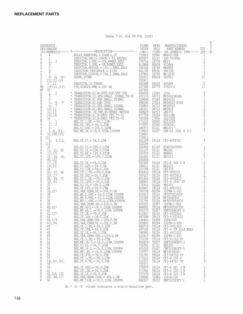
REPLACEMENT PARTS
7-58
Table 7-14. A14 FM PCA (cont)
REFERENCEDESIGNATOR-A>-NUMERICS---->KLLLLLLLLLMPMPQQQQQQQQQRRRRRRRRRRRRRRRRRRRRRRRRRRRRRRRRRRRRRRRRRRRRRRRRRRR
412, 345678- 16, 18-20,22-2417,2119-21,23-281, 2345, 8, 96, 7
10,1112,1314,15161, 72, 345, 6,31,
32,108,110,1118, 9,112,
1131011, 21, 2212,1513, 14, 16,60,12217,1918,202425, 67, 8626,2728, 29, 7330,50333435,1073637383940,1274142,1374344,11945,94464748495152535455565758,65,90,93596162,128, 13063, 88,11764
S--------------DESCRIPTION--------------RELAY,ARMATURE,2 FORM C,5VINDUCTOR,VAR,0.194UH,+-5%,SHLDEDINDUCTOR,3.3UH,+-10%,88MHZ,SHLDINDUCTOR,3.9UH,+-5%,84MHZ,SHLDINDUCTOR,6800UH,+-10%,1.5MHZ,SHLDINDUCTOR,VARIABLE,4.61UHINDUCTOR,2200UH,+-10%,2.2MHZ,SHLDCHOKE,6TURN
INDUCTOR, 10 TURNSPIN,SINGLE,PWB,0.025 SQ
* TRANSISTOR,SI,N-JFET,UHF/VHF USE* TRANSISTOR,SI,NPN,SMALL SIGNAL,TO-92* TRANSISTOR,SI,PNP,SMALL SIGNAL* TRANSISTOR,SI,PNP,T092* TRANSISTOR,SI,NPN,SMALL SIGNAL* TRANSISTOR,SI,NPN,SMALL SIGNAL* TRANSISTOR, SI,PNP,HI-SPEED SWITCH* TRANSISTOR,SI,N-DMOS FET,TO-72* TRANSISTOR,SI,N-DMOS FET,TO-72RES,CF,1.8K,+-5%,0.25WRES,CF,360,+-5%,0.25WRES,CC,10K,+-10%,0.125WRES,MF,2K,+-1%,0.125W,100PPM
RES,CF,47,+-5%,0.25W
RES,CC,15,+-10%,0.125WRES,CC,10,+-10%,0.125WRES,CC,68,+-10%,0.125WRES,CC,100,+-10%,0.125W
RES,CF,56,+-5%,0.25WRES,CC,220,+-5%,0.5WRES,CC,13K,+-5%,0.25WRES,CF,1.5K,+-5%,0.25WRES,CF,360,+-5%,0.25WRES,CF,2.2K,+-5%,0.25WRES,CF,100K,+-5%,0.25WRES,CC,33,+-10%,0.125WRES,CF,100,+-5%,0.25WRES,VAR,CERM,1K,+-10%,0.5WRES,MF,2.49K,+-1%,0.125W,100PPMRES,MF,4.99K,+-1%,0.125W,100PPMRES,MF,5.49K,+-1%,0.125W,100PPMRES,VAR,CERM,5K,+-10%,0.5WRES,MF,453,+-1%,0.125W,100PPMRES,MF,68.1,+-1%,0.125W,100PPMRES,CF,2K,+-5%,0.25WRES,CF,24K,+-5%,0.25WRES,VAR,CERM,20K,+-20%,0.5WRES,VAR,CERM,50,+-20%,0.5WRES,CF,2.4K,+-5%,0.25WRES,CF,10K,+-5%,0.25WRES,CF,1K,+-5%,0.25WRES,VAR,CERM,50K,+-20%,0.5WRES,CF,1.2K,+-5%,0.25WRES,MF,36.5,+-1%,0.125W,100PPMRES,CC,43,+-5%,0.125WRES,MF,39.2,+-1%,0.125W,100PPMRES,MF,182,+-1%,0.125W,100PPMRES,CF,47K,+-5%,0.25WRES,CF,1.5K,+-5%,0.25WRES,CF,4.7K,+-5%,0.25W
RES,CF,820,+-5%,0.25WRES,CF,10K,+-5%,0.25WRES,CF,1K,+-5%,0.25WRES,VAR,CERM,100K,+-30%,0.5WRES,MF,150K,+-1%,0.125W,100PPM
FLUKESTOCK
- --NO--733063845057174714413864363184861138147801320911320911463448267500267500403634832170229898698290330803248351369629477729783308573220573097246975719815719815719815822189822189261800321125261818261826261826641068186031221598810432747527851840658963272914810465393728810523721548721795493593866681855270810457697599234443320861866710697102780585225417573196855259715391855262719757721787573212721571721571574970573394573170193045866327
MFRSSPLY
-CODE-5198402113247598953624759895362475989536
8953600779
12040047130726327014047130471304713183241785665940659400112191637
59124
81349011210112101121
59124011210112159124591245912459124011221591248029459124591245912432997591249163759124591245140680294591245912459124802945912491637011219163759124591245912459124
5912459124591247298291637
MANUFACTURERSPART NUMBER
-OR GENERIC TYPE-----MR602-5SR142-05J08SMR33413864MR6800861138MR-2200320911
46344887623-1
J310MPS652ORLRAMPS6522MPS6562-D262MPS6560MPS9182N5771SD213EESD215DER25J182R25K361BB1031CMF-55 2001 F T-1
CF1-4VT470J
RCR05G150KSBB1001BB6801BB1011
CF1-4 560 J BEB2215CB1335CF1-4VT152CF1-4VT361JCF1-4VT222JCF1-4-104J VTBB3301CF1-4VT101J3299W-1-102VF50VTD2491FMF55D4991FMF50VTD5491F3299W-1-502MF50VDT4530FCMF5568R1FT-1CF1-4VT202JCF1-4-VT243J332H/2033329H-1-500CF1-4VT242JCF1-4 VT 103J REELCF1-4VT102J3329H-1-503CF1/4-122-5%CMF5536R5FT-1BB4305CMF5539R2FT-1MF55D1820FCF1-4473J VTCF1-4 152 JCF1-4472J VT
CF1-4 821 J BCF1-4 103 J BCF1-4 102 J B3221H-104CMF551503FT-1
TOT- QTY-
1121111
15
211
2113222212217
4
1325
22132321121111212122111111111114
11331
N0T-E-
An * in 'S' column indicates a static-sensitive part.
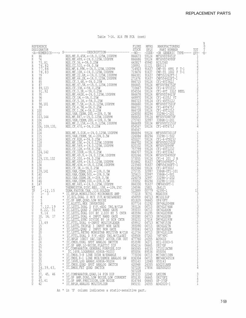
REPLACEMENT PARTS
7-59
Tab1e 7-14. A14 FM PCA (cont)
REFERENCEDESIGNATOR-A>-NUMERICS---->RRRRRRRRRRRRRRRRRRRRRRRRRRRRRRRRRRRRRRRRRRTTPUUUUUUUUUUUUUUUUUUUUUUUUUUUUU
667475,8176,8277,8478,837980858789,12391,9295969798,10199
100102103,144104105106, 109,135,136114115116118120121124,142126129,131,132133134138139,14114014514614711-12,151- 34567,12,198,22, 519,14
10, 16, 171113,491518202123242527293032333536,39,43,4737, 45, 463840,4142
An
S--------------DESCRIPTION--------------RES,MF,8.45K,+-1%,0.125W,100PPMRES,MF,499,+-1%,0.125W,100PPMRES,CF,36,+-5%,0.25WRES,CC,510,+-5%,0.5WRES,MF,4.99K,+-1%,0.125W,100PPMRES,MF,10K,+-1%,0.125W,100PPMRES,MF,22.6K,+-1%,0.125W,100PPMRES,MF,44.2K,+-1%,0.125W,100PPMRES,CF,3.6K,+-5%,0.25WRES,MF,47.5K,+-1%,0.125W,100PPMRES,CF,33K,+-5%,0.25WRES,CF,3.3K,+-5%,0.25WRES,MF,442K,+-1%,0.125W,100PPMRES,CF,1M,+-5%,0.25WRES,CF,5.1K,+-5%,0.25WRES,MF,7.5K,+-1%,0.125W,100PPMRES,CF,4.7M,+-5%,0.25WRES,CF,1.2M,+-5%,0.25WRES,VAR,CERM, 200, +-20%, 0. 5WRES,MF,887,+-1%,0.125W,100PPMRES,VAR,CERM, 200, +-10%, 0. 5WRES,MF,2.15K,+-1%,0.125W,100PPMRES,CF,470,+-5%,0.25W
RES,MF,3.01K,+-1%,0.125W,100PPMRES,VAR,CERM, 5K,+-20%,0.5WRES,CF,82K,+-5%,0.25WRES,MF,15K,+-1%,0.125W,100PPMRES,MF,549,+-1%,0.125W,100PPMRES,CF,12K,+-5%,0.25WRES,CF,330K,+-5%,0.25WRES,MF,49.9,+-1%,0.125W,100PPMRES,CF,200,+-5%,0.25WRES,MF,499,+-1%,0.125W,100PPMRES,MF,634,+-1%,0.125W,100PPMRES,CF,3K,+-5%,0.25WRES,VAR,CERM,100,+-10%,0.5WRES,VAR,CERM,500,+-10%,0.5WRES,VAR,CERM,2K,+-20%,0.5WRES,VAR,CERM,100,+-20%,0.5WRES,MF,665,+-1%,0.125W,100PPMTHERMISTOR,DISC,NEG.,10K,+-10%,25CTERM,FASTON,TAB,.110,SOLDER
* IC,BPLR,MONOLITHIC MICROWAVE AMP* IC,ECL,DUAL D M/S F/F,W/SET&RESET* IC,OP AMP,QUAD,LOW NOISE* IC,ALSTTL,HEX INVERTERS* IC,LSTTL,DUAL D F/F,+EDG TRG,W/CLR* IC,LSTTL,QUAD 2 INPUT NAND GATE* IC,LSTTL,DUAL DIV BY 2,DIV BY 5 CNTR* IC,LSTTL,DUAL 4 INPUT NAND GATE* IC,LSTTL,SYNC DIVIDE BY 16 BIN CNTR* IC,FTTL,DUAL 4-INPUT MULTIPLEXER* IC,LSTTL,TRIPLE 3 INPUT NOR GATE* IC,LSTTL,QUAD 2 INPUT NOR GATE* IC,LSTTL,RETRG MONOSTAB MULTIVB W/CLR* IC,FTTL,DUAL D F/F,+EDG TRG,W/CL&SET* IC,BPLR 10BIT DAC,10BIT ACCUR,CUR OUT* IC,CMOS,DUAL SPDT ANALOG SWITCH* IC,OP AMP,LO-NOISE,PLASTIC DIP* IC,COMPARATOR,GENERAL PURPOSE,DIP* IC,16V8,LOGARRAY,6080A-90203* IC,CMOS,3-8 LINE DCDR W/ENABLE* IC,CMOS,8-1 LINE MUX/DEMUX ANALOG SW* IC,16V8,LOG ARRAY,6080A-90204* IC,CMOS,QUAD SPST ANALOG SWITCH* IC,DMOS,FET QUAD SWITCH** IC,COMPARATOR,QUAD,14 PIN DIP* IC,OP AMP,DUAL,LOW NOISE,LOW CURRENT* IC,OP AMP,PRECISION,LOW NOISE* IC,BPLR,ANALOG MULTIPLIER
FLUKESTOCK--NO--866673866686643817108951714923719476866301271676866715866665733667854554866678649970866723866660866731866728226050866652275743866699854567854567866694226084655027866702820332757799866707820266573055816462223560810366275735325613226076193052866330104596512889773218454959851829837716393124393033483594393280393231659912393090393041412734659508477760853598854216845065855056773036836304855143620948507228507228387233855130816744845151
MFRSSPLY
-CODE-5912459124659400112191637916379163791637591245912459124591245912459124591245912459124591248029459124329975912459124
591248029459124591245912459124591245912459124916379163759124329973299732997802949163715801007797E7510471306665012920471304713012950471327014047130471304713047130726324355343710666564155895360471304713120402435517856
12040066650666524355
MANUFACTURERSPART NUMBER
-OR GENERIC TYPE-----MF50VDT8451FMF50VDT4990FR25J360EB5115CMF-55 4991 F T-1CMF-55 1002 F T-1CMF552262FT-1CMF554422FT-1CF1-4VT362JMF50VTB4752FCF1-4-VT333JCF1-4VT 332J REELMF50VDT4423FCF1-4105J VTCF1-4VT512JMF50VDT7501FCF1-4VT475JCF1-4VT125J3329H-1-201MF50VTD8870F3386R-1-201MF50VDT2151FCF1-4VT471J
MF50VDT3011F3329H-1-502CF1-4-VT823JMF50VDD1502FMF50VTD549FCF1-4VT123JCF1-4VT334JMF50VTD4992FCF1-4 201 J BCMF554990FT-1CMF556340FT-1CF1-4VT302J3386R-OT1-1013386R-1-5013329H-1-2023329H-1-101CMF6650FT-1JA41J162395-1MSA0304MC10131POP470FYSN74ALS04BNSN74LS74ANSN74LSOONSN74LS390NSN74LS20NDM74LS193NMC74F153NSN74LS27NSN74LS02NSN74LS122N74F74PCAD561DHI1-0303-5OP27GPLT1011ACN8855056MC74HC138NMM74HC4051N855143ADG201AKNSSD500203
LM339NOP270FZOP-37GPAD42020-1
TOTQTY-
11222211112211121112114
11111121311121111113311133231211111111111114
3121
N0T-E-
* in 'S' column indicates a static-sensitive part.
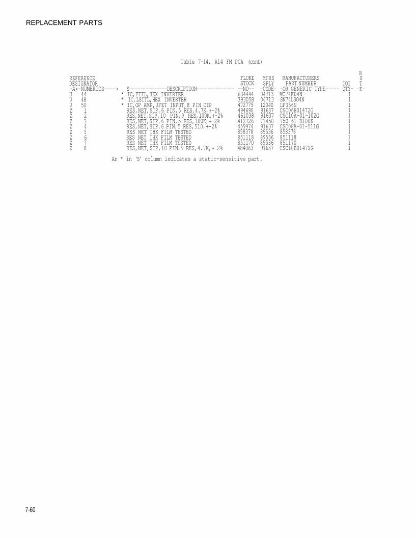
REPLACEMENT PARTS
7-60
Tab1e 7-14. A14 FM PCA (cont)
REFERENCEDESIGNATOR-A>-NUMERICS----> S--------------DESCRIPTION--------------UUUZZZZZZZZ
44485012345678
* IC,FTTL,HEX INVERTER* IC,LSTTL,HEX INVERTER* IC,OP AMP,JFET INPUT,8 PIN DIPRES,NET,SIP,6 PIN,5 RES,4.7K,+-2%RES,NET,SIP,10 PIN,9 RES,100K,+-2%RES,NET,SIP,6 PIN,5 RES,100K,+-2%RES,NET,SIP,6 PIN,5 RES,510,+-2%RES NET THK FILM TESTEDRES NET THK FILM TESTEDRES NET THK FILM TESTEDRES,NET,SIP,10 PIN,9 RES,4.7K,+-2%
FLUKESTOCK--NO--634444393058472779494690461038412726459974858378851118851170484063
MFRSSPLY-CODE-0471304713120409163791637714509163789536895368953691637
MANUFACTURERSPART NUMBER
-OR GENERIC TYPE-----MC74F04NSN74LSO4NLF356NCSC06B01472GCSC10A-01-102G750-61-R100KCSC08A-01-511G858378851118851170CSC10B01472G
TOTQTY-
11111111111
N0T-E-
An * in 'S' column indicates a static-sensitive part.
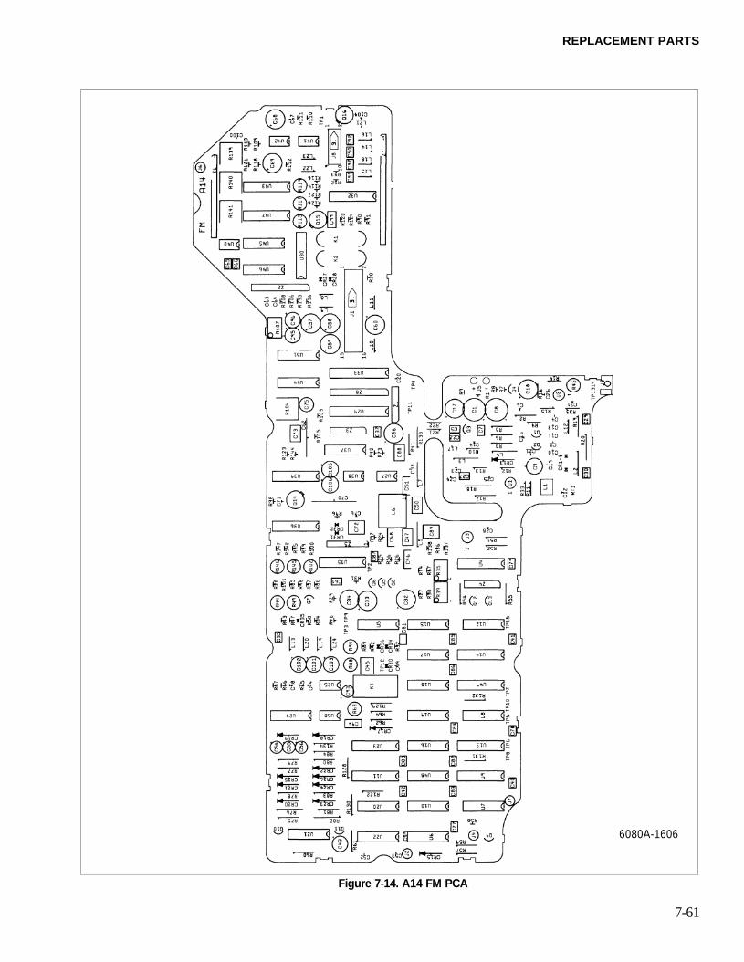
REPLACEMENT PARTS
6080A-1606
Figure 7-14. A14 FM PCA
7-61
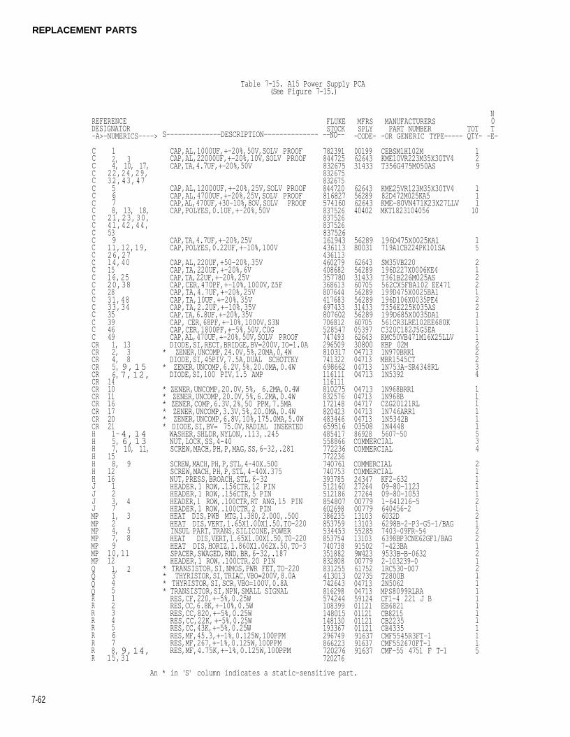
REPLACEMENT PARTS
7-62
Table 7-15. A15 Power Supp1y PCA(See Figure 7-15.)
REFERENCEDESIGNATOR-A>-NUMERICS---->
CCCCCCCCCCCCCCCCCCCCCCCCCCCRCRCRCRCRCRCRCRCRCRCRCRHHHHHHHJJJJMPMPMPMPMPMPMPQQQQRRRRRRRRR
12, 34, 10, 17,
22,24,29,32,43,475678, 13, 18,21,23,30,41,42,44,539
11,12,19,26,2714,401516,2520,382831,4833,34353946491, 132, 34, 85, 9,156, 7,12,
141011161720211- 4,145, 6,137, 10, 11,
158, 9
1216123, 471, 324, 57, 89
10,11121, 234512345678, 9,14,
15,31
S--------------DESCRIPTION--------------
CAP,AL,1000UF,+-20%,50V,SOLV PROOFCAP,AL,22000UF,+-20%,10V,SOLV PROOFCAP,TA,4.7UF,+-20%,50V
CAP,AL,12000UF,+-20%,25V,SOLV PROOFCAP,AL,4700UF,+-20%,25V,SOLV PROOFCAP,AL,470UF,+30-10%,8OV,SOLV PROOFCAP,POLYES,0.1UF,+-20%,50V
CAP,TA,4.7UF,+-20%,25VCAP,POLYES,0.22UF,+-10%,100V
CAP,AL,220UF,+50-20%,35VCAP,TA,220UF,+-20%,6VCAP,TA,22UF,+-20%,25VCAP,CER,470PF,+-10%,1000V,Z5FCAP,TA,4.7UF,+-20%,25VCAP,TA,10UF,+-20%,35VCAP,TA,2.2UF,+-10%,35VCAP,TA,6.8UF,+-20%,35VCAP, CER,68PF,+-10%,1000V,S3NCAP,CER,1800PF,+-5%,50V,C0GCAP,AL,470UF,+-20%,50V,SOLV PROOFDIODE,SI,RECT,BRIDGE,BV=200V,IO=1.0A
* ZENER,UNCOMP,24.0V,5%,20MA,0,4WDIODE,SI,45PIV,7.5A,DUAL SCHOTTKY
* ZENER,UNCOMP,6.2V,5%,20.0MA,0.4WDIODE,SI,100 PIV,1.5 AMP
* ZENER,UNCOMP,20.0V,5%, 6.2MA,0.4W* ZENER,UNCOMP,20.0V,5%,6.2MA,0.4W* ZENER,COMP,6.3V,2%,50 PPM,7.5MA* ZENER,UNCOMP,3.3V,5%,20.0MA,0.4W* ZENER,UNCOMP,6.8V,10%,175.0MA,5.0W* DIODE,SI,BV= 75.0V,RADIAL INSERTEDWASHER,SHLDR,NYLON,.113,.245NUT,LOCK,SS,4-40SCREW,MACH,PH,P,MAG,SS,6-32,.281
SCREW,MACH,PH,P,STL,4-40X.500SCREW,MACH,PH,P,STL,4-40X.375NUT,PRESS,BROACH,STL,6-32HEADER,1 ROW,.156CTR,12 PINHEADER,1 ROW,.156CTR,5 PINHEADER,1 ROW,.100CTR,RT ANG,15 PINHEADER,1 ROW,.100CTR,2 PINHEAT DIS,PWB MTG,1.380,2.000,.500HEAT DIS,VERT,1.65X1.00X1.50,TO-220INSUL PART,TRANS,SILICONE,POWERHEAT DIS,VERT,1.65X1.00X1.50,T0-220HEAT DIS,HORIZ,1.860X1.062X.50,TO-3SPACER,SWAGED,RND,BR,6-32,.187HEADER,1 ROW,.100CTR,20 PIN
* TRANSISTOR,SI,NMOS,PWR FET,TO-220* THYRISTOR,SI,TRIAC,VBO=200V,8.0A* THYRISTOR,SI,SCR,VBO=100V,0.8A* TRANSISTOR,SI,NPN,SMALL SIGNALRES,CF,220,+-5%,0.25WRES,CC,6.8K,+-10%,0.5WRES,CC,820,+-5%,0.25WRES,CC,22K, +-5%,0.25WRES,CC,43K,+-5%,0.25WRES,MF,45.3,+-1%,0.125W,100PPMRES,MF,267,+-1%,0.125W,100PPMRES,MF,4.75K,+-1%,0.125W,100PPM
FLUKESTOCK--NO--
782391844725832675832675832675844720816827574160837526837526837526837526161943436113436113460279408682357780368613807644417683697433807602706812528547747493296509810317741322698662116111116111810275832576172148820423483446659516485417558866772236772236740761740753393785512160512186854807602698386235853759534453853754740738351882832808831255413013742643816298574244108399148015148130193367296749866223720276720276
MFRSSPLY-CODE-
001996264331433
62643562896264340402
5628980031
62643562893143360705562895628931433562896070505397626433080004713047130471304713
04713047130471704713047130350886928
MANUFACTURERSPART NUMBER
-OR GENERIC TYPE-----
CEBSM1H102MKME10VR223M35X30TV4T356G475M050AS
KME25VR123M35X30TV482D472M025KA5KME-80VN471K23X27LLVMKT1823104056
196D475X0025KA1719A1CB224PK101SA
SM35VB220196D227X0006KE4T361B226M025AS562CX5FBA102 EE471199D475X0025BA1196D106X0035PE4T356E225K035AS199D685X0035DA1561CR3LRE102EE680KC320C182J5G5EAKMC50VB471M16X25LLVKBP 02M1N970BRR1MBR1545CT1N753A-SR4348RL1N5392
1N968BRR11N968BCZG20121RL1N746ARR11N5342B1N44485607-50
COMMERCIALCOMMERCIAL
COMMERCIALCOMMERCIAL243472726427264007790077913103131035528513103915029W42300779617520273504713047135912401121011210112101121916379163791637
KF2-63209-80-112309-80-10531-641216-5640456-26032D6298B-2-P3-G5-1/BAG7403-09FR-546398BP3CNE62GF1/BAG7-423BA9533B-B-06322-103239-01RC530-007T2800B2N5062MPS8099RLRACF1-4 221 J BEB6821CB8215CB2235CB4335CMF5545R3FT-1CMF552670FT-1CMF-55 4751 F T-1
TOTQTY-
129
11110
15
2122122111122234
111111534
21111212122121211111111115
N0T-E-
An * in 'S' column indicates a static-sensitive part.
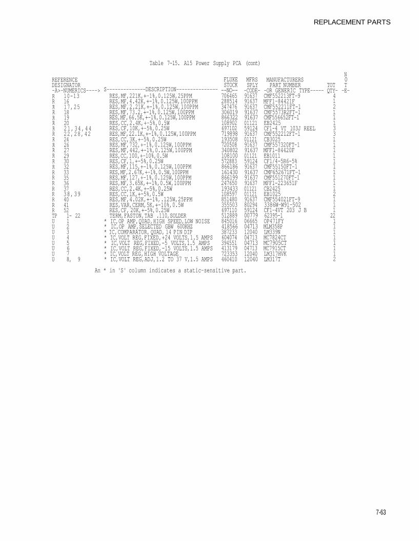
REPLACEMENT PARTS
7-63
Table 7-15. A15 Power Supply PCA (cont)
REFERENCEDESIGNATOR-A>-NUMERICS---->RRRRRRRRRRRRRRRRRRRRRRTPUUUUUUUU
10-131617,2518192021,34,4422,28,422426272930323335363738,394041521- 2212345678, 9
S--------------DESCRIPTION---------------RES,MF,221K,+-1%,0.125W,25PPMRES,MF,4.42K,+-1%,0.125W,100PPMRES,MF,2.21K,+-1%,0.125W,100PPMRES,MF,73.2,+-1%,0.125W,100PPMRES,MF,66.5K,+-1%,0.125W,100PPMRES,CC,2.4K,+-5%,0.5WRES,CF,10K,+-5%,0.25WRES,MF,22.1K,+-1%,0.125W,100PPMRES,CC,3K,+-5%,0.25WRES,MF,732,+-1%,0.125W,100PPMRES,MF,442,+-1%,0.125W,100PPMRES,CC,100,+-10%,0.5WRES,CF,1,+-5%,0.25WRES,MF,115,+-1%,0.125W,100PPMRES,MF,2.67K,+-1%,0.5W,100PPMRES,MF,127,+-1%,0.125W,100PPMRES,MF,3.65K,+-1%,0.5W,100PPMRES,CC,2.4K,+-5%,0.25WRES,CC,1K,+-5%,0.5WRES,MF,4.02K,+-1%,.125W,25PPMRES,VAR,CERM,5K,+-10%,0.5WRES,CF, 20K,+-5%,0.25WTERM,FASTON,TAB .110,SOLDER
* IC,OP AMP,QUAD,HIGH SPEED,LOW NOISE* IC,OP AMP,SELECTED GBW 600KHZ* IC,COMPARATOR, QUAD, 14 PIN DIP* IC,VOLT REG,FIXED,+24 VOLTS,1.5 AMPS* IC,VOLT REG,FIXED,-5 VOLTS,1.5 AMPS* IC,VOLT REG,FIXED,-15 VOLTS,1.5 AMPS* IC,VOLT REG,HIGH VOLTAGE* IC,VOLT REG,ADJ,1.2 TO 37 V,1.5 AMPS
FLUKESTOCK--NO--706465288514347476306019866322108902697102719898193508720508340802108100572883866186161430866199247650193433108597851480355503697110512889845016418566387233604074394551413179723353460410
MFRSSPLY
-CODE-91637916379163791637916370112159124916370112191637916370112159124916379163791637916370112101121916378029459124007790666504713120400471304713047131204012040
MANUFACTURERSPART NUMBER
-OR GENERIC TYPE-----CMF552213FT-9MFF1-84421FCMF552211FT-1CMF5573R2FT-1CMF556652FT-1EB2425CF1-4 VT 103J REELCMF552212FT-1CB3025CMF557320FT-1MFF1-84420FEB1011CF1/4-5R6-5%CMF55150FT-1CMF652671FT-1CMF551270FT-1MFF1-223651FCB2425EB1025CMF554021FT-93386W-W91-502CF1-4VT 203 J B62395-1OP471FYMLM358PLM339NMC7824CTMC7905CTMC7915CTLM317HVKLM317T
TOTQTY-
41211133111111111121112211111112
N0T-E-
An * in 'S' column indicates a static-sensitive part.
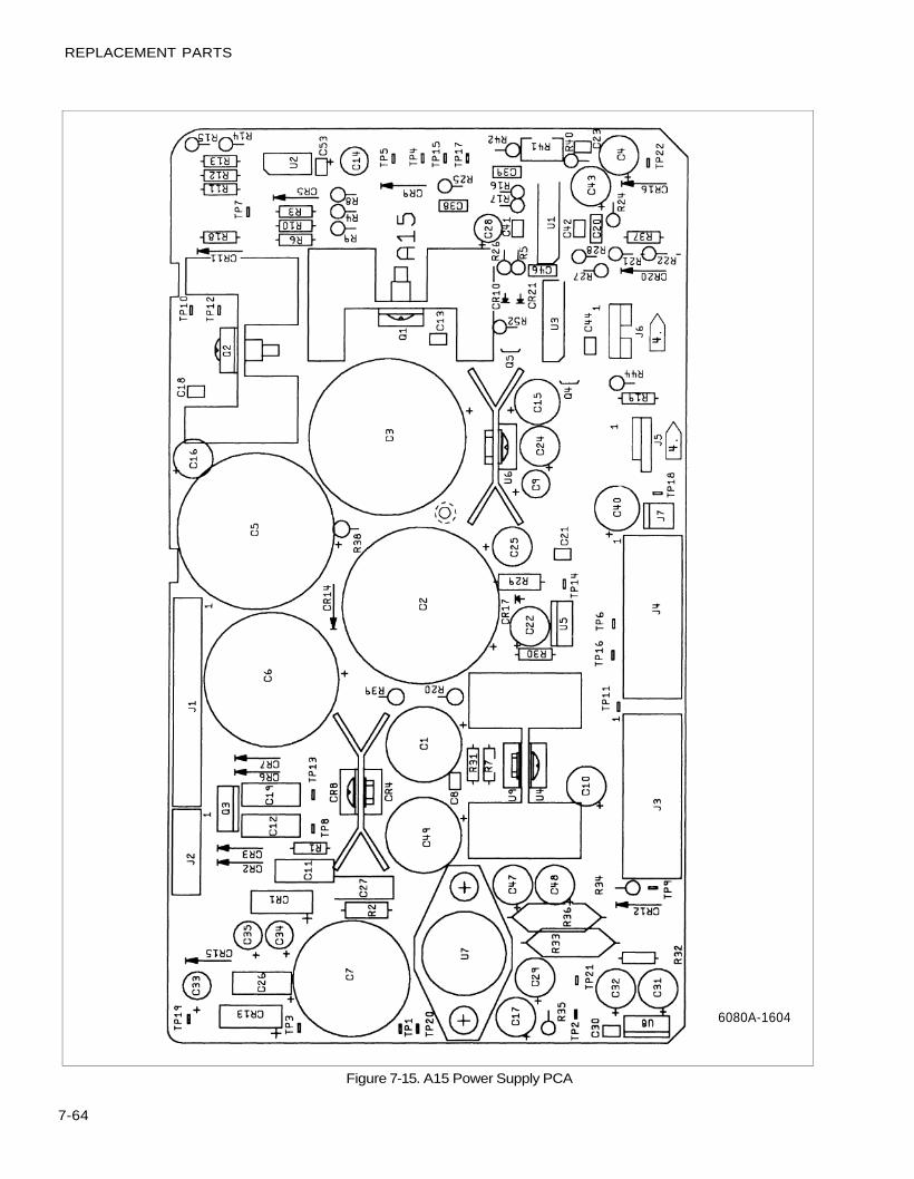
REPLACEMENT PARTS
7-64
Figure 7-15. A15 Power Supply PCA
6080A-1604
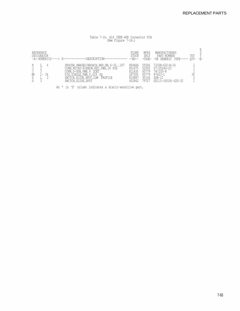
REPLACEMENT PARTS
7-65
Table 7-l6. A16 IEEE-488 Connector PCA(See Figure 7-16.)
REFERENCEDESIGNATOR-A>-NUMERICS---->
H 3, 4J 2J 3MP 1- 34S 1, 2S 3
S--------------DESCRIPTION--------------
SPACER,SWAGED/BROACH,RND,BR,6-32,.187CONN,MICRO-RIBBON,REC,PWB,24 POSCONN,D-SUB,PWB,9 SCKTPIN,SINGLE,PWB,0.025 SQSWITCH,SLIDE,SPDT,LOW PROFILESWITCH,SLIDE,DPDT
FLUKESTOCK
--NO--
854666851675811430267500810887452862
MFRSSPLY
-CODE-
555665250000779007799514679727
MANUFACTURERSPART NUMBER
-OR GENERIC TYPE-----
7332B-632-B-1457-20240-23747150-887623-1SSB-12GS113-(0018)-G20-32
TOTQTY-
211
3421
N0T-E-
An * in 'S' column indicates a static-sensitive part.
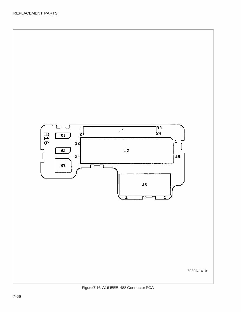
REPLACEMENT PARTS
7-66
Figure 7-16. A16 IEEE -488 Connector PCA
6080A-1610
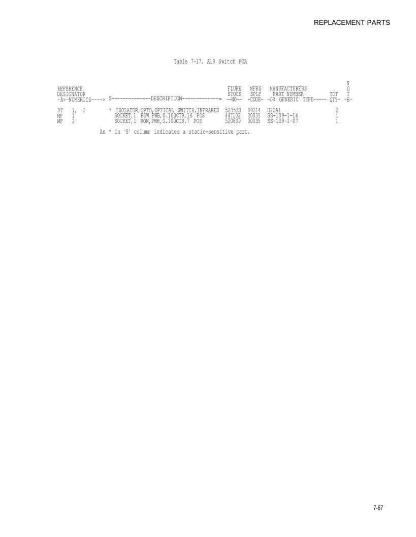
REPLACEMENT PARTS
7-67
Table 7-17. A19 Switch PCA
REFERENCEDESIGNATOR-A>-NUMERICS---->
DTMPMP
1, 212
S--------------DESCRIPTION--------------
* ISOLATOR,OPTO,OPTICAL SWITCH,INFRAREDSOCKET,1 ROW,PWB,0.100CTR,16 POSSOCKET,1 ROW,PWB,0.100CTR,7 POS
FLUKESTOCK
- --NO--
523530447102520809
MFRSSPLY
-CODE-
092143003530035
MANUFACTURERSPART NUMBER
-OR GENERIC TYPE-----
H22A1SS-109-1-16SS-109-1-07
TOTQTY-
211
N0T-E-
An * in 'S' column indicates a static-sensitive part.
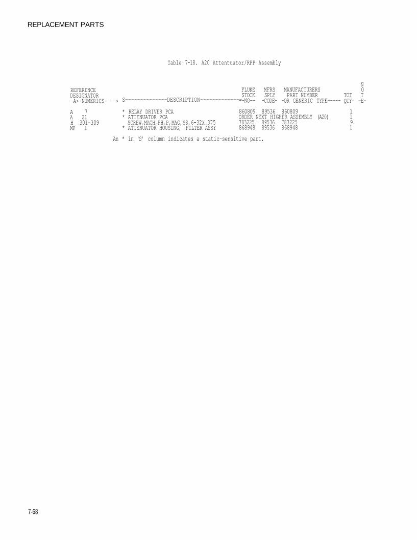
REPLACEMENT PARTS
7-68
Table 7-18. A20 Attentuator/RPP Assembly
REFERENCEDESIGNATOR-A>-NUMERICS---->
A 7A 21H 301-309MP 1
S--------------DESCRIPTION--------------
* RELAY DRIVER PCA* ATTENUATOR PCASCREW,MACH,PH,P,MAG,SS,6-32X.375
* ATTENUATOR HOUSING, FILTER ASSY
FLUKESTOCK--NO--
860809
MFRSSPLY
-CODE-
89536
MANUFACTURERSPART NUMBER
-OR GENERIC TYPE-----
860809ORDER NEXT HIGHER ASSEMBLY (A20)783225868948
8953689536
783225868948
TOTQTY-
1191
N0T-E-
An * in 'S' column indicates a static-sensitive part.
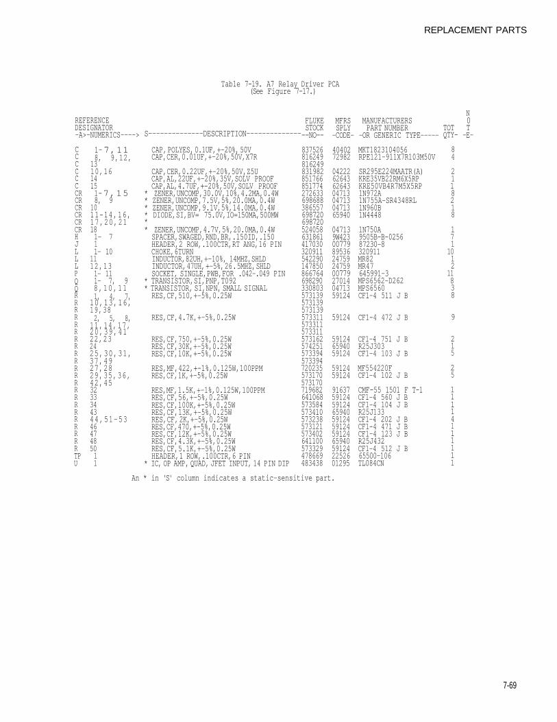
REPLACEMENT PARTS
7-69
Tab1e 7-19. A7 Re1ay Driver PCA(See Figure 7-17.)
REFERENCEDESIGNATOR-A>-NUMERICS---->
CCCCCCCRCRCRCRCRCRHJLLLPQQRRRRRRRRRRRRRRRRRRRRRRTPU
1- 7,118, 9,12,
1310,1614151- 7,158, 9
1011-14,16,17,20,21181- 711- 10
1112,131- 111- 7, 98,10,111, 4, 7,10,13,16,19,382, 5, 8,
11,14,17,20,39,4122,232425,30,31,37,4927,2829,35,36,42,453233344344,51-534647485011
S--------------DESCRIPTION--------------
CAP, POLYES, 0.1UF, +-20%, 50VCAP,CER,0.01UF,+-20%,50V,X7R
CAP,CER,0.22UF,+-20%,50V,Z5UCAP,AL,22UF,+-20%,35V,SOLV PROOFCAP,AL,4.7UF,+-20%,50V,SOLV PROOF
* ZENER,UNCOMP,30.0V,10%,4.2MA,0.4W* ZENER,UNCOMP,7.5V,5%,20.0MA,0.4W* ZENER,UNCOMP,9.1V,5%,14.0MA,0.4W* DIODE,SI,BV= 75.0V,IO=150MA,500MW** ZENER,UNCOMP,4.7V,5%,20.0MA,0.4WSPACER,SWAGED,RND,BR,.150ID,.150HEADER,2 ROW,.100CTR,RT ANG,16 PINCHOKE,6TURNINDUCTOR,82UH,+-10%, 14MHZ,SHLDINDUCTOR, 47UH, +-5%, 26 . 5MHZ, SHLDSOCKET, SINGLE,PWB,FOR .042-.049 PIN
* TRANSISTOR,SI,PNP,T092* TRANSISTOR, SI,NPN, SMALL SIGNALRES,CF,510,+-5%,0.25W
RES,CF,4.7K,+-5%,0.25W
RES,CF,750,+-5%,0.25WRES,CF,30K,+-5%,0.25WRES,CF,10K,+-5%,0.25W
RES,MF,422,+-1%,0.125W,100PPMRES,CF,1K,+-5%,0.25W
RES,MF,1.5K,+-1%,0.125W,100PPMRES,CF,56,+-5%,0.25WRES,CF,100K,+-5%,0.25WRES,CF,13K,+-5%,0.25WRES,CF, 2K,+-5%,0.25WRES,CF,470,+-5%,0.25WRES,CF,12K,+-5%,0.25WRES,CF,4.3K,+-5%,0.25WRES,CF,5.1K,+-5%,0.25WHEADER,1 ROW,.100CTR,6 PIN
* IC, OP AMP, QUAD, JFET INPUT, 14 PIN DIP
FLUKESTOCK--NO--
837526816249816249831982851766851774272633698688386557698720698720524058631861417030320911542290147850866764698290330803573139573139573139573311573311573311573162574251573394573394720235573170573170719682641068573584573410573238573121573402641100573329478669483438
MFRSSPLY
-CODE-
4040272982
04222626436264304713047130471365940
047139W4230077989536247592475900779270140471359124
59124
591246594059124
5912459124
9163759124591246594059124591245912465940591242252601295
MANUFACTURERSPART NUMBER
-OR GENERIC TYPE-----
MKT1823104056RPE121-911X7R103M50V
SR295E224MAATR(A)KRE35VB22RM6X5RP
TOTQTY-
84
21
KRE50VB4R7M5X5RP 11N972A 81N755A-SR4348RL 21N960B1N4448
1N750A
18
19505B-B-0256 787230-8320911MR82MR47645991-3
11012
11
N0T-E-
MPS6562-D262 8MPS6560CF1-4 511 J B
CF1-4 472 J B
CF1-4 751 J BR25J303CF1-4 103 J B
MF554220FCF1-4 102 J B
CMF-55 1501 F T-1CF1-4 560 J BCF1-4 104 J BR25J133CF1-4 202 J BCF1-4 471 J BCF1-4 123 J BR25J432CF1-4 512 J B65500-106TL084CN
38
9
215
25
11114111111
An * in 'S' column indicates a static-sensitive part.
REPLACEMENT PARTS
7-70
Figure 7-17. A7 Relay Driver PCA
6080A-1604
REPLACEMENT PARTS
7-71
Table 7-20. A21 Attenuator PCA(See Figure 7-18.)
REFERENCEDESIGNATOR-A>-NUMERICS---->
CCCCRCRHJJKPRRRRRRRRRRRR
1, 2, 43, 56, 712- 91- 8121- 81- 111, 4, 7,
10,192, 3, 5,6, 8, 9,
11,12,20,211314,151617,182223
S--------------DESCRIPTION--------------
CAP,CER,1000PF,+-20%,50V,X7R,0805CAP,TA,4.7UF,+-10%,15VCAP,TA,3.3UF,+-20%,50V
* DIODE,SI,SCHOTTKY BARRIER,SMALL SIGNL* DIODE,SI,BV= 70.0V,500 MWRELAY WASHERSOCKET,SINGLE,PWB,FOR 0.034-0.037 PINCONN,COAX,SMA(M),PWB OR PANELRELAY, SCREENED, HIGH FREQUENCYSOCKET,SINGLE, PWB,FOR .042-.049 PINRES,MF,402,+-0.5%,0.125W,50PPM
RES,MF,56.9,+-0.5%,0.125W,50PPM
RES,MF,37.4,+-0.5%,0.125W,50PPMRES,MF,150,+-0.5%,0.125W,50PPMRES,MF,94.2,+-0.5%,0.125W,50PPMRES,MF,83.5,+-0.5%,0.125W,50PPMRES,MF,10K,+-1%,0.25W,100PPMRES,CF, 51,+-5%,0.25W
FLUKESTOCK--NO--
514059519363772848535195454181803247732826512087812669544056461632461632461590461590461590461590461079461624461616461608799635572990
MFRSSPLY
-CODE-
0539733297562892848003508
MANUFACTURERSPART NUMBER
-OR GENERIC TYPE-----
C0805C102M5XATNSC475K15195D335X0050Z25082-28001N4606
COMMERCIAL0077921845895360077903888
89536
038880388889536895367159059124
2-332070-72985-601181266950871-1PME60-4020DP-2
461590
PME60-37R4DP-2PME60-1500DP-24616164616085063JD1002FCF1-4 510 J B
TOTQTY-
322188118
115
10
121211
N0T-E-
An * in 'S' column indicates a static-sensitive part.
REPLACEMENT PARTS
7-72
Figure 7-18. A21 Attentuator PCA
6080A-1636
MANUFACTURER'S FEDERAL SUPPLY CODES
55680Nichicon/America/Corp.Schaumburg, IL
56289Sprague Electric Co.North Adams,MA
57693Oscillatek Corp.Olathe, KS
59124KOA-Speer Electronics Inc.Bradford, PA
59365Metelics Corp.Sunnyvale, CA
60705Cera-Mite Corp.(formerly: Sprague)Grafton, Wl
60935Westlake Capacitor Inc.Tantalum Div.Greencastle, IN
61058Matsushita Electric Corp.of AmericaPanasonic Industrial Co. Div.Secaucus, NJ
61271Fujitsu Microelectronics Inc.San Jose, CA
61752IR-ONICS Inc.Warwick, Rl
61804M/A-Com, Inc.Burlington, MA
62643United ChemiconRosemont, IL
64155Linear TechnologyMilpitas, CA
65940Rohm Corp. & WhatneyIrvine, CA
65964Evox Inc.Bannockburn, IL
66419ExelSan Jose, CA
66675Lattice Semiconductor Corp.Hillsboro, OR
68919WIMAHarry Levinson Co.Seattle, WA
7E751Avantek, Inc.Santa Clara, CA
70903Cooper-Belden Corp.Geneva, IL
71034Bliley Electric Co.Erie, PA
71400Bussman ManufacturingDiv. McGraw-Edison Co.St. Louis, MO
71450CTS Corp.Elkhart, IN
71590Mepco/CentralabA North American Philips Co.Fort Dodge, IA
72259Nytronics Inc.New York, NY
72962Elastic Stop NutDiv. of Harrard IndustriesUnion, NJ
72982Erie Specialty Products, Inc.(formerly: Murata Erie)Erie, PA
73734Federal Screw Products Inc.Chicago, IL
74840Illinois Capacitor Inc.Lincolnwood, IL
79727C - W IndustriesSouthampton, PA
8C798Ken-Tronics, Inc.Milan, IL
80031Mepco/Electra Inc.Morristown, NJ
80294Bourns Instruments Inc.Riverside, CA
83330Kulka Smith Inc.A North American Philips Co.Manasquan, NJ
84411American ShizukiTRW Capacitors Div.Ogallala, NE
86928Seastrom Mfg. Co. Inc.Glendale, CA
89536John Fluke Mfg. Co., Inc.Everett, WA
9W423AmatomEl Mont, CA
91293Johanson Mfg. Co.Boonton, NJ
91502Associated MachineSanta Clara, CA
91506Augat AlcoswitchNorth Andover, MA
91637Dale Electronics Inc.Columbus, NE
95146Alco Electronic Products Inc.Switch DivisionNorth Andover, MA
95275Vitramon Inc.Bridgeport, CT
96881Thomson Industries Inc.Port Washington, NY
98159Rubber-Teck Inc.Gardena, CA
98291Sealectro Corp.BICC ElectronicsTrumbill, CT
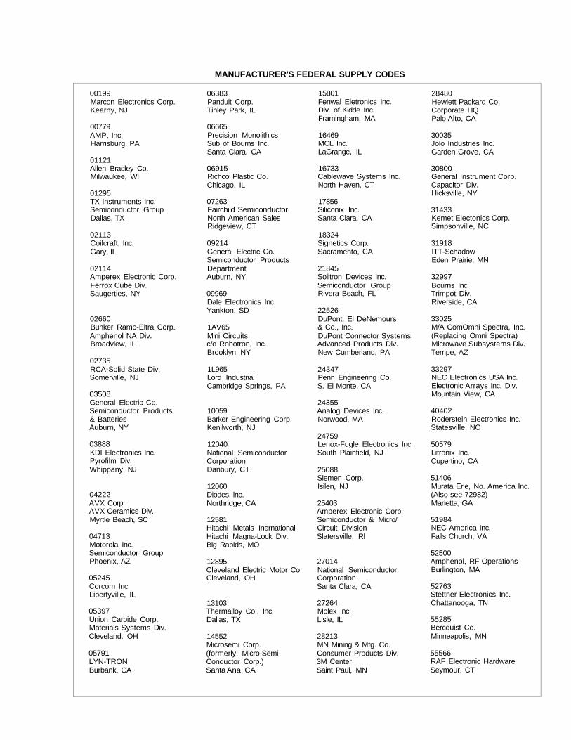
MANUFACTURER'S FEDERAL SUPPLY CODES
00199Marcon Electronics Corp.Kearny, NJ
00779AMP, Inc.Harrisburg, PA
01121Allen Bradley Co.Milwaukee, Wl
01295TX Instruments Inc.Semiconductor GroupDallas, TX
02113Coilcraft, Inc.Gary, IL
02114Amperex Electronic Corp.Ferrox Cube Div.Saugerties, NY
02660Bunker Ramo-Eltra Corp.Amphenol NA Div.Broadview, IL
02735RCA-Solid State Div.Somerville, NJ
03508General Electric Co.Semiconductor Products& BatteriesAuburn, NY
03888KDI Electronics Inc.Pyrofilm Div.Whippany, NJ
04222AVX Corp.AVX Ceramics Div.Myrtle Beach, SC
04713Motorola Inc.Semiconductor GroupPhoenix, AZ
05245Corcom Inc.Libertyville, IL
05397Union Carbide Corp.Materials Systems Div.Cleveland. OH
05791LYN-TRONBurbank, CA
06383Panduit Corp.Tinley Park, IL
06665Precision MonolithicsSub of Bourns Inc.Santa Clara, CA
06915Richco Plastic Co.Chicago, IL
07263Fairchild SemiconductorNorth American SalesRidgeview, CT
09214General Electric Co.Semiconductor ProductsDepartmentAuburn, NY
09969Dale Electronics Inc.Yankton, SD
1AV65Mini Circuitsc/o Robotron, Inc.Brooklyn, NY
1L965Lord IndustrialCambridge Springs, PA
10059Barker Engineering Corp.Kenilworth, NJ
12040National SemiconductorCorporationDanbury, CT
12060Diodes, lnc.Northridge, CA
12581Hitachi Metals InernationalHitachi Magna-Lock Div.Big Rapids, MO
12895Cleveland Electric Motor Co.Cleveland, OH
13103Thermalloy Co., Inc.Dallas, TX
14552Microsemi Corp.(formerly: Micro-Semi-Conductor Corp.)Santa Ana, CA
15801Fenwal Eletronics Inc.Div. of Kidde Inc.Framingham, MA
16469MCL Inc.LaGrange, IL
16733Cablewave Systems Inc.North Haven, CT
17856Siliconix Inc.Santa Clara, CA
18324Signetics Corp.Sacramento, CA
21845Solitron Devices Inc.Semiconductor GroupRivera Beach, FL
22526DuPont, El DeNemours& Co., Inc.DuPont Connector SystemsAdvanced Products Div.New Cumberland, PA
24347Penn Engineering Co.S. El Monte, CA
24355Analog Devices Inc.Norwood, MA
24759Lenox-Fugle Electronics Inc.South Plainfield, NJ
25088Siemen Corp.Isilen, NJ
25403Amperex Electronic Corp.Semiconductor & Micro/Circuit DivisionSlatersville, Rl
27014National SemiconductorCorporationSanta Clara, CA
27264Molex Inc.Lisle, IL
28213MN Mining & Mfg. Co.Consumer Products Div.3M CenterSaint Paul, MN
28480Hewlett Packard Co.Corporate HQPalo Alto, CA
30035Jolo Industries Inc.Garden Grove, CA
30800General Instrument Corp.Capacitor Div.Hicksville, NY
31433Kemet Electonics Corp.Simpsonville, NC
31918ITT-SchadowEden Prairie, MN
32997Bourns Inc.Trimpot Div.Riverside, CA
33025M/A ComOmni Spectra, Inc.(Replacing Omni Spectra)Microwave Subsystems Div.Tempe, AZ
33297NEC Electronics USA Inc.Electronic Arrays Inc. Div.Mountain View, CA
40402Roderstein Electronics Inc.Statesville, NC
50579Litronix Inc.Cupertino, CA
51406Murata Erie, No. America Inc.(Also see 72982)Marietta, GA
51984NEC America Inc.Falls Church, VA
52500Amphenol, RF OperationsBurlington, MA
52763Stettner-Electronics Inc.Chattanooga, TN
55285Bercquist Co.Minneapolis, MN
55566RAF Electronic HardwareSeymour, CT
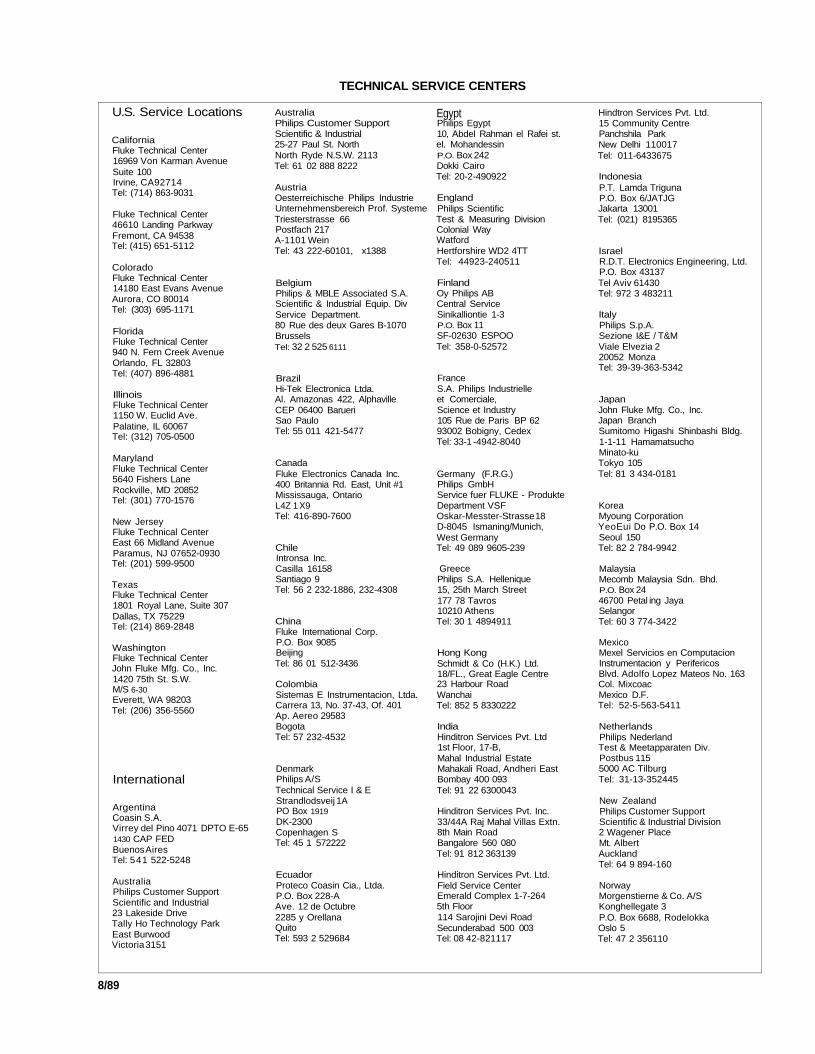
TECHNICAL SERVICE CENTERS
8/89
U.S. Service Locations
CaliforniaFluke Technical Center16969 Von Karman AvenueSuite 100Irvine, CA92714Tel: (714) 863-9031
Fluke Technical Center46610 Landing ParkwayFremont, CA 94538Tel: (415) 651-5112
ColoradoFluke Technical Center14180 East Evans AvenueAurora, CO 80014Tel: (303) 695-1171
FloridaFluke Technical Center940 N. Fern Creek AvenueOrlando, FL 32803Tel: (407) 896-4881
IllinoisFluke Technical Center1150 W. Euclid Ave.Palatine, IL 60067Tel: (312) 705-0500
MarylandFluke Technical Center5640 Fishers LaneRockville, MD 20852Tel: (301) 770-1576
New JerseyFluke Technical CenterEast 66 Midland AvenueParamus, NJ 07652-0930Tel: (201) 599-9500
TexasFluke Technical Center1801 Royal Lane, Suite 307Dallas, TX 75229Tel: (214) 869-2848
WashingtonFluke Technical CenterJohn Fluke Mfg. Co., Inc.1420 75th St. S.W.M/S 6-30Everett, WA 98203Tel: (206) 356-5560
International
ArgentinaCoasin S.A.Virrey del Pino 4071 DPTO E-651430 CAP FEDBuenos AiresTel: 541 522-5248
AustraliaPhilips Customer SupportScientific and Industrial23 Lakeside DriveTally Ho Technology ParkEast BurwoodVictoria 3151
AustraliaPhilips Customer SupportScientific & Industrial25-27 Paul St. NorthNorth Ryde N.S.W. 2113Tel: 61 02 888 8222
AustriaOesterreichische Philips IndustrieUnternehmensbereich Prof. SystemeTriesterstrasse 66Postfach 217A-1101 WeinTel: 43 222-60101, x1388
BelgiumPhilips & MBLE Associated S.A.Scientific & Industrial Equip. DivService Department.80 Rue des deux Gares B-1070BrusselsTel: 32 2 525 6111
BrazilHi-Tek Electronica Ltda.Al. Amazonas 422, AlphavilleCEP 06400 BarueriSao PauloTel: 55 011 421-5477
CanadaFluke Electronics Canada Inc.400 Britannia Rd. East, Unit #1Mississauga, OntarioL4Z 1 X9Tel: 416-890-7600
ChileIntronsa Inc.Casilla 16158Santiago 9Tel: 56 2 232-1886, 232-4308
ChinaFluke International Corp.P.O. Box 9085BeijingTel: 86 01 512-3436
ColombiaSistemas E Instrumentacion, Ltda.Carrera 13, No. 37-43, Of. 401Ap. Aereo 29583BogotaTel: 57 232-4532
DenmarkPhilips A/STechnical Service I & EStrandlodsveij 1APO Box 1919DK-2300Copenhagen STel: 45 1 572222
EcuadorProteco Coasin Cia., Ltda.P.O. Box 228-AAve. 12 de Octubre2285 y OrellanaQuitoTel: 593 2 529684
EgyptPhilips Egypt10, Abdel Rahman el Rafei st.el. MohandessinP.O. Box 242Dokki CairoTel: 20-2-490922
EnglandPhilips ScientificTest & Measuring DivisionColonial WayWatfordHertforshire WD2 4TTTel: 44923-240511
FinlandOy Philips ABCentral ServiceSinikalliontie 1-3P.O. Box 11SF-02630 ESPOOTel: 358-0-52572
FranceS.A. Philips Industrielleet Comerciale,Science et Industry105 Rue de Paris BP 6293002 Bobigny, CedexTel: 33-1 -4942-8040
Germany (F.R.G.)Philips GmbHService fuer FLUKE - ProdukteDepartment VSFOskar-Messter-Strasse 18D-8045 Ismaning/Munich,West GermanyTel: 49 089 9605-239
GreecePhilips S.A. Hellenique15, 25th March Street177 78 Tavros10210 AthensTel: 30 1 4894911
Hong KongSchmidt & Co (H.K.) Ltd.18/FL., Great Eagle Centre23 Harbour RoadWanchaiTel: 852 5 8330222
IndiaHinditron Services Pvt. Ltd1st Floor, 17-B,Mahal Industrial EstateMahakali Road, Andheri EastBombay 400 093Tel: 91 22 6300043
Hinditron Services Pvt. Inc.33/44A Raj Mahal Villas Extn.8th Main RoadBangalore 560 080Tel: 91 812 363139
Hinditron Services Pvt. Ltd.Field Service CenterEmerald Complex 1-7-2645th Floor114 Sarojini Devi RoadSecunderabad 500 003Tel: 08 42-821117
Hindtron Services Pvt. Ltd.15 Community CentrePanchshila ParkNew Delhi 110017Tel: 011-6433675
IndonesiaP.T. Lamda TrigunaP.O. Box 6/JATJGJakarta 13001Tel: (021) 8195365
IsraelR.D.T. Electronics Engineering, Ltd.P.O. Box 43137Tel Aviv 61430Tel: 972 3 483211
ItalyPhilips S.p.A.Sezione I&E / T&MViale Elvezia 220052 MonzaTel: 39-39-363-5342
JapanJohn Fluke Mfg. Co., Inc.Japan BranchSumitomo Higashi Shinbashi Bldg.1-1-11 HamamatsuchoMinato-kuTokyo 105Tel: 81 3 434-0181
KoreaMyoung CorporationYeoEui Do P.O. Box 14Seoul 150Tel: 82 2 784-9942
MalaysiaMecomb Malaysia Sdn. Bhd.P.O. Box 2446700 Petal ing JayaSelangorTel: 60 3 774-3422
MexicoMexel Servicios en ComputacionInstrumentacion y PerifericosBlvd. Adolfo Lopez Mateos No. 163Col. MixcoacMexico D.F.Tel: 52-5-563-5411
NetherlandsPhilips NederlandTest & Meetapparaten Div.Postbus 1155000 AC TilburgTel: 31-13-352445
New ZealandPhilips Customer SupportScientific & Industrial Division2 Wagener PlaceMt. AlbertAucklandTel: 64 9 894-160
NorwayMorgenstierne & Co. A/SKonghellegate 3P.O. Box 6688, RodelokkaOslo 5Tel: 47 2 356110
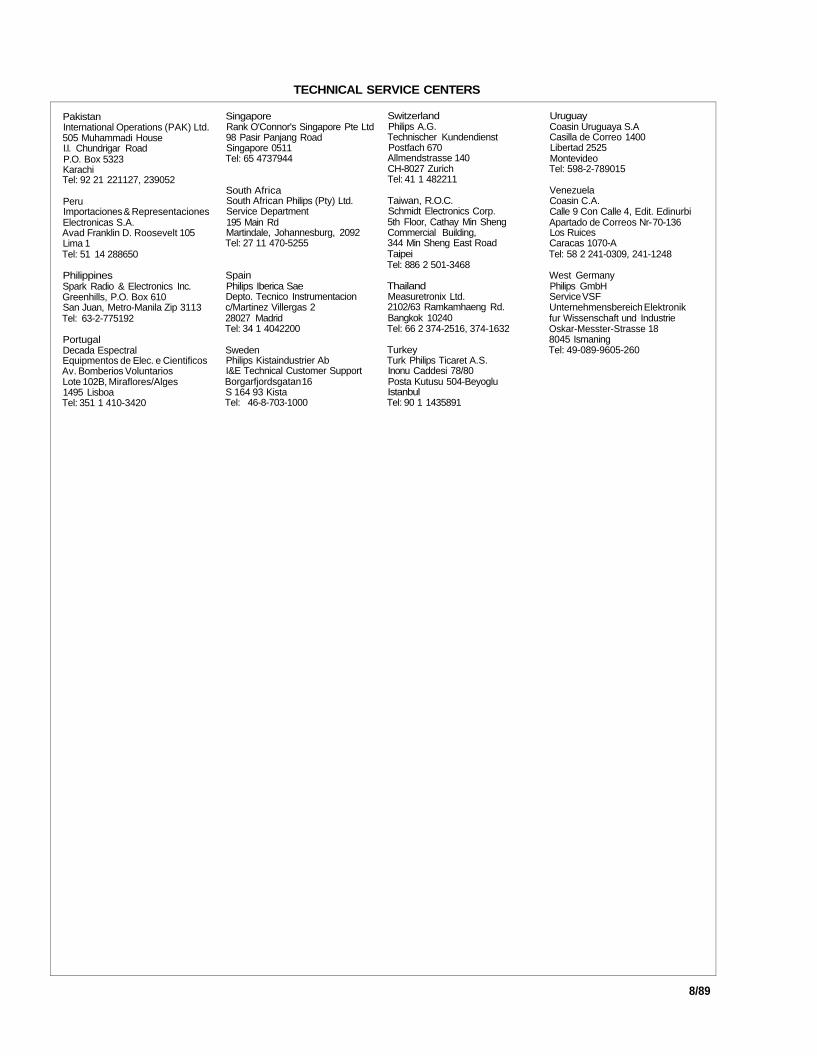
TECHNICAL SERVICE CENTERS
8/89
PakistanInternational Operations (PAK) Ltd.505 Muhammadi HouseI.I. Chundrigar RoadP.O. Box 5323KarachiTel: 92 21 221127, 239052
PeruImportaciones & RepresentacionesElectronicas S.A.Avad Franklin D. Roosevelt 105Lima 1Tel: 51 14 288650
PhilippinesSpark Radio & Electronics Inc.Greenhills, P.O. Box 610San Juan, Metro-Manila Zip 3113Tel: 63-2-775192
PortugalDecada EspectralEquipmentos de Elec. e CientificosAv. Bomberios VoluntariosLote 102B, Miraflores/Alges1495 LisboaTel: 351 1 410-3420
SingaporeRank O'Connor's Singapore Pte Ltd98 Pasir Panjang RoadSingapore 0511Tel: 65 4737944
South AfricaSouth African Philips (Pty) Ltd.Service Department195 Main RdMartindale, Johannesburg, 2092Tel: 27 11 470-5255
SpainPhilips Iberica SaeDepto. Tecnico Instrumentacionc/Martinez Villergas 228027 MadridTel: 34 1 4042200
SwedenPhilips Kistaindustrier AbI&E Technical Customer SupportBorgarfjordsgatan 16S 164 93 KistaTel: 46-8-703-1000
SwitzerlandPhilips A.G.Technischer KundendienstPostfach 670Allmendstrasse 140CH-8027 ZurichTel: 41 1 482211
Taiwan, R.O.C.Schmidt Electronics Corp.5th Floor, Cathay Min ShengCommercial Building,344 Min Sheng East RoadTaipeiTel: 886 2 501-3468
ThailandMeasuretronix Ltd.2102/63 Ramkamhaeng Rd.Bangkok 10240Tel: 66 2 374-2516, 374-1632
TurkeyTurk Philips Ticaret A.S.Inonu Caddesi 78/80Posta Kutusu 504-BeyogluIstanbulTel: 90 1 1435891
UruguayCoasin Uruguaya S.ACasilla de Correo 1400Libertad 2525MontevideoTel: 598-2-789015
VenezuelaCoasin C.A.Calle 9 Con Calle 4, Edit. EdinurbiApartado de Correos Nr- 70-136Los RuicesCaracas 1070-ATel: 58 2 241-0309, 241-1248
West GermanyPhilips GmbHService VSFUnternehmensbereich Elektronikfur Wissenschaft und IndustrieOskar-Messter-Strasse 188045 IsmaningTel: 49-089-9605-260


