Embed Size (px)
Citation preview

www.elsevier.com/locate/cplett
Chemical Physics Letters 402 (2005) 340–345
Meso- and nano-scale investigation of carbon fibers coated bynano-crystalline diamond
M. Rossi a, M.L. Terranova b,*, S. Piccirillo b, V. Sessa b, D. Manno c
a Dipartimento di Energetica, Universita �La Sapienza� and Unita INFM-RM1, Via A.Scarpa 14, 00161 Roma, Italyb Dipartimento di Scienze e Tecnologie Chimiche and INSTM, Universita �Tor Vergata�, Via della Ricerca Scientifica, 00133 Roma, Italy
c Dipartimento di Scienza dei Materiali and Unita INFM-Lecce, Universita di Lecce, Via Arnesano, 00133 Lecce, Italy
Received 20 October 2004; in final form 13 December 2004
Available online 4 January 2005
Abstract
A morphological–structural investigation regarding the coating of vapour grown carbon fibers (VGCF) by polycrystalline dia-
mond layers, produced by CVD activation of CH4/H2 mixtures is reported. Transmission electron microscopy (TEM) and electron
diffraction (ED) techniques allowed detailing, for the first time at nanoscale, the morphology and structure of different carbon layers
across the 3-D geometry of the diamond coated fibers. Our results indicate an isotropic distribution of the various carbon phases
along the direction transversal to the fiber axis, and the occurrence of turbostratic graphite layers at the fiber/diamond interface
region. The diamond coating is formed by nano-grains with sizes ranging between 5 and 50 nm and substantially free of extended
defects.
� 2004 Elsevier B.V. All rights reserved.
1. Introduction
Carbon fibers represent an extremely important tech-
nological material [1] and extensive efforts have been
dedicated over the past decade to the research and devel-
opment of new types of meso- and micro-structured Cfibers [2,3].
Exploiting potential applications in various strategic
fields, such as energy saving, thermal management and
space technology, caused researchers to develop strate-
gies apt to produce meso- and micro-sized fibers with
enhanced properties in terms of hardness, chemical
inertness, high thermal conductivity, high sputter-resis-
tance [4,5].The coupling of carbon fibers with diamond, indeed,
may offer significant advantages. However, one major
concern in producing diamond-coated micro-sized car-
0009-2614/$ - see front matter � 2004 Elsevier B.V. All rights reserved.
doi:10.1016/j.cplett.2004.12.052
* Corresponding author.
E-mail addresses: �[email protected] (M.L.
Terranova).
bon fibers is the strong control of the structural features
of the outermost diamond phase in terms of size, texture
and crystalline quality of grains, but also of the inner
fiber at the end of the coating process. Diamond-coated
carbon-fibers can be considered an innovative diamond-
based composite material for which many possible tech-nological applications can be envisaged [6–10].
In the present Letter, the coating of vapour grown car-
bon fibers by layers of nanocrystalline diamond is
reported. In particular, we investigated and identified
the stacking sequence of the different carbon-based mate-
rial when diamond coating of a carbon fiber is carried out.
VGCF fibers were chosen in view of their outstanding
properties (in primis thermal and electrical conductivity)which make them a widely used functional material [11].
2. Experimental
The objective of our research was to monitor the sta-
bility of the fibers under the conditions of the CVD

M. Rossi et al. / Chemical Physics Letters 402 (2005) 340–345 341
process, to investigate the crystallographic features of
the deposited diamond phase and to detail the micro-
structure of the fiber/diamond systems.
The nanocrystalline diamond deposits have been pro-
duced by CVD technique on isolate fibers, as well as on
textures formed by woven filaments. The deposition runswere performed in a hot filament CVD reactor using
CH4/H2 mixtures. A detailed description of our deposi-
tion system can be found in [12]. The fibers were
like-amorphous VGCFs; we used fibers from different
production stocks with diameters ranging between
7.5 and 15 lm, preliminarily submitted to a seeding
pre-treatment by placing them in an ultrasonic cleaner
with a suspension of fine-grained diamond powders (witha mean size d < 0.25 lm) in hexane. We used ad hoc
designed fiber-holders, screwed at the standard DC-
heated sample holder, to keep the fibers at controlled dis-
tance and position with respect to the heated Ta filament.
The filament temperature, kept at 2200 ± 10 �C, was
monitored by a two-colour optical pyrometer. We sub-
mitted to the coating process single and textured fibers.
In particular, the single carbon fibers have beenmechanically separated by the textured material and
manipulated by using a suitable microtweezers system
under a optical microscope.
In case of single fiber coating, the fiber has been
clamped at the extremities, kept parallel to the filament
at a distance of about 6 mm and heated combining
Joule-effect and heating from the standard sample
holder at a distance of about 1 mm. The relatively lim-ited diameter of the fibers helps to achieve a uniform dis-
tribution of the coating that is carried out under the
Fig. 1. SEM images of: (a) and (b) typical textured array of as-received VGC
single fiber, mechanically detached from its textured array, before (c) and af
typical conditions of a chemical vapour deposition. In
case of textured fibers, the rectangular shaped samples,
with sizes of 2 · 15 mm, were always clamped at the
extremities and kept aligned (along the larger side) to
the filament and vertically positioned (in other words,
sample and filament were in the same vertical plane dur-ing the deposition process).
Several experiments have been performed by varying
the fibers temperature between 650 and 750 �C and
using active gas phases containing CH4/H2 ratios be-
tween 0.5% and 2.0%. The flow rate of the CH4/H2 mix-
tures was fixed at 150 sccm (standard cubic centimeters
per minute), and the pressure in the deposition chamber
was 30 Torr. The experimental set-up allowed a com-plete and uniform coating of the fibers during a single
deposition run, lasting 1 h.
The general shape of the fibers before diamond coat-
ing was observed by SEM (scanning electron
microscopy).
A JEOL 2010 electron microscope operating at
160 kV was used to carry out HRTEM (high resolution
transmission electron microscopy) investigations inbright field mode and TED (transmission electron dif-
fraction) analysis. In particular we used a TEM espe-
cially configured for convergent beam electron
diffraction (CBED) observation with a double tilting
system, allowing a sample tilting of ±60�, particularlysuitable to check the homogeneity of the deposits along
the radial direction.
The obtained HRTEM micrographs have been suc-cessively digitized and filtered in the spatial frequency
field in order to improve the signal-to-noise ratio. The
Fs before (a) and after (b) the diamond deposition process; (c) and (d)
ter (d) the diamond deposition process.

342 M. Rossi et al. / Chemical Physics Letters 402 (2005) 340–345
TED (transmission electron diffraction) patterns were
obtained in selected area electron diffraction (SAED)
conditions.
The RHEED (reflection high energy electron diffrac-
tion) analysis has been performed at variable angles
using a TEM-EM6G apparatus operating at 60 kVand equipped with a high resolution diffraction goniom-
eter stage.
Fig. 2. (a) and (b) Diffraction analysis: experimental SAED pattern (a)
taken from the edge of a single-coated carbon fiber. The comparison (b)
of experimental and [13] interplanar distances and indexing puts in
evidence that all the electron diffraction signals belong to the diamond
phase (s.g. Fd3m). (c)–(f) HRTEM analysis: images (c) and (e), at
increasing magnification, from the outermost polycrystalline diamond
film covering the VGC fiber after CVD processing. Bragg-filtered image
(f) of a single diamond nanograin, from the region evidenced in (e).
3. Results and discussion
The results reported in this Section refer to sample
produced using a 0.5% CH4 in H2 and at substrate tem-perature of 650 �C. These were, indeed, the suitable
experimental conditions for the formation of nanosized
diamond.
The SEM images of Fig. 1 shows the typical morpho-
logies of as-received textured (a and b) and single (c and
d) VGCFs, before (a and c) and after (b and d) diamond
deposition. The fibers were originally assembled as a
cross-texture and the structural analysis by electron dif-fraction did not reveal any presence of crystalline order,
within the sensitivity limit of the used experimental
techniques.
A series of detailed morphological and structural
investigations have been carried out by HRTEM and
TED on deposits obtained on single fibers. Isolated fi-
bers, mechanically detached from the textured substrate,
were also analysed, without revealing detectabledifferences.
The studies by electron diffraction (in both transmis-
sion and reflection conditions) have been performed on
the longitudinal edge of the diamond-coated fibers in or-
der to deduce microstructure and relative location of the
various carbon phases.
The analysis of the SAED patterns produced by the
outermost layers of the material (Fig. 2a and b) indicatesthe presence of the set of Debye�s rings characteristic ofthe diamond phase (s.g. Fd3m); the experimental inter-
planar spacings are found to match with the diamond
reference values [13] within 1% uncertainty. The
HRTEM images of Fig. 2c–f display, at increasing mag-
nification, the morphological features of the outermost
polycrystalline deposits. The SAED and HRTEM anal-
ysis reveal that the outermost layers are formed by dia-mond crystallites with size ranging between about 5 and
50 nm. The digital image processing allows an easy
evaluation of the high crystalline quality of the single
nano-grains. Fig. 2f shows a typical single grain after
digital filtering, evidencing a crystal lattice substantially
lacking of extended defects.
Going on through the outer periphery of the coated
fibers towards the inner core fibers, the ED pattern re-veals the presence of additional diffraction signals, evi-
denced by arrows in the ED pattern of Fig. 3a, that
can be rationalized taking into account the contempo-
rary presence of two different phases in the region inter-
acting with the e-beam. The set of diffraction rings
belongs to diamond phase, while the diffraction arcs
indicate the presence of a different and partially oriented
crystalline phase with an interplanar distance of about
3.43 A, near to the 0002 d-spacing of graphite [13]. By
considering that in the experimental approach thee-beam is driven to a direction normal to the fiber axis,
from the outermost region towards the fiber core, from
the transmission electron diffraction pattern analysis we
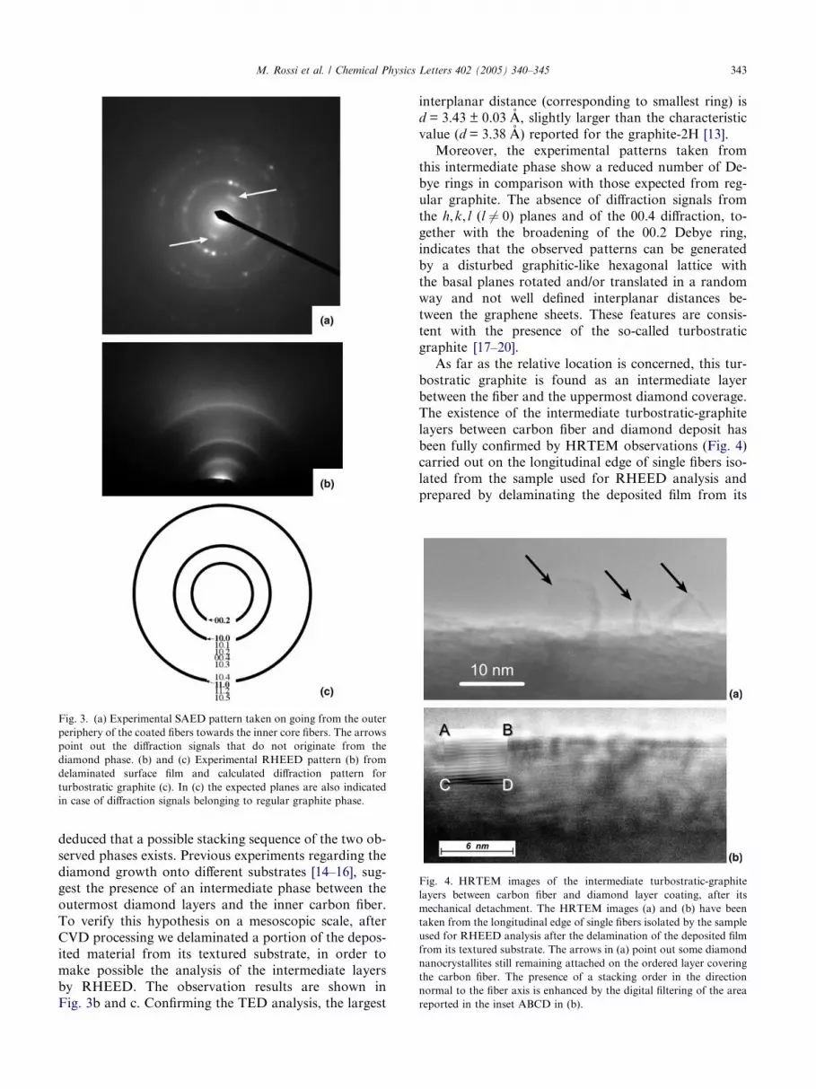
Fig. 4. HRTEM images of the intermediate turbostratic-graphite
layers between carbon fiber and diamond layer coating, after its
mechanical detachment. The HRTEM images (a) and (b) have been
taken from the longitudinal edge of single fibers isolated by the sample
used for RHEED analysis after the delamination of the deposited film
from its textured substrate. The arrows in (a) point out some diamond
nanocrystallites still remaining attached on the ordered layer covering
the carbon fiber. The presence of a stacking order in the direction
normal to the fiber axis is enhanced by the digital filtering of the area
reported in the inset ABCD in (b).
Fig. 3. (a) Experimental SAED pattern taken on going from the outer
periphery of the coated fibers towards the inner core fibers. The arrows
point out the diffraction signals that do not originate from the
diamond phase. (b) and (c) Experimental RHEED pattern (b) from
delaminated surface film and calculated diffraction pattern for
turbostratic graphite (c). In (c) the expected planes are also indicated
in case of diffraction signals belonging to regular graphite phase.
M. Rossi et al. / Chemical Physics Letters 402 (2005) 340–345 343
deduced that a possible stacking sequence of the two ob-
served phases exists. Previous experiments regarding the
diamond growth onto different substrates [14–16], sug-gest the presence of an intermediate phase between the
outermost diamond layers and the inner carbon fiber.
To verify this hypothesis on a mesoscopic scale, after
CVD processing we delaminated a portion of the depos-
ited material from its textured substrate, in order to
make possible the analysis of the intermediate layers
by RHEED. The observation results are shown in
Fig. 3b and c. Confirming the TED analysis, the largest
interplanar distance (corresponding to smallest ring) is
d = 3.43 ± 0.03 A, slightly larger than the characteristic
value (d = 3.38 A) reported for the graphite-2H [13].
Moreover, the experimental patterns taken from
this intermediate phase show a reduced number of De-
bye rings in comparison with those expected from reg-ular graphite. The absence of diffraction signals from
the h,k, l (l 6¼ 0) planes and of the 00.4 diffraction, to-
gether with the broadening of the 00.2 Debye ring,
indicates that the observed patterns can be generated
by a disturbed graphitic-like hexagonal lattice with
the basal planes rotated and/or translated in a random
way and not well defined interplanar distances be-
tween the graphene sheets. These features are consis-tent with the presence of the so-called turbostratic
graphite [17–20].
As far as the relative location is concerned, this tur-
bostratic graphite is found as an intermediate layer
between the fiber and the uppermost diamond coverage.
The existence of the intermediate turbostratic-graphite
layers between carbon fiber and diamond deposit has
been fully confirmed by HRTEM observations (Fig. 4)carried out on the longitudinal edge of single fibers iso-
lated from the sample used for RHEED analysis and
prepared by delaminating the deposited film from its

Fig. 5. Schematic axial- and side-view of a single coated carbon fibre (T = 650 �C, 1% CH4/H2), summarizing the location of the different carbon
material, as deduced on the base of electron microscopy and diffraction observations. The sizes of the three different regions are not in scale; the true
sizes are: Region a (inner core): carbon fiber, with diameters ranging between 10 and 15 lm; Region b (intermediate layer): turbostratic graphite, with
an average thickness of about 7 nm; Region c (outermost coating): polycrystalline nanodiamond with an estimated thickness of about 200 nm.
344 M. Rossi et al. / Chemical Physics Letters 402 (2005) 340–345
textured substrate. The delamination of diamond coat-
ings can be easily achieved by strongly bending the sam-
ple, taking advantage of the different elastic propertiesof carbon fibers and diamond; moreover, after this first
mechanical detachment, the samples are ultrasonically
treated. This two steps process allows us achieving an
almost complete detachment of diamond coating.
On the edge of the delaminated fiber some diamond
nanocrystallites are still visible and grown on an ordered
layer covering the carbon fiber, as evidenced by arrows
in Fig. 4a.The presence of a stacking order in the direction nor-
mal to the fiber axis is strongly evidenced by the digital
filtering of the area reported in the inset ABCD of Fig.
4b. The analysis of HRTEM images reveals that the lat-
tice planes are characterized by an interplanar distance
of about 3.45 ± 0.05 A, in good agreement with electron
diffraction measurements. The average thickness of the
intermediate graphitic layer is of about 7 nm (with min-imum and maximum measured value of 5 and 10 nm,
respectively).
The results summarized in Figs. 2–4 remain substan-
tially unchanged tilting the fibers on a transversal plane
to the fiber-axis and containing the e-beam direction.
The homogeneous results obtained from observations
at different tilting angles of diametrically opposed exter-
nal areas of different fibers allow us deducing the pres-ence of an isotropic radial distribution of the different
carbon phases.
The overall fiber/diamond systems result in consisting
mainly of 3 materials, as indicated in the schematic view
sketched in Fig. 5:
(a) An inner core formed by the carbon fiber, which
still maintains the original structure.(b) An intermediate layer formed by turbostratic
graphite, with an average thickness of about 7 nm.
(c) The outermost coating formed by nano-sized dia-
mond crystals without any preferential crystallo-
graphic orientation; the estimated thickness of thepolycrystalline diamond layer is about 200 nm.
4. Conclusions
In the course of the present research proper proce-
dures have been selected for the coating of carbon fibersby homogeneous diamond layers formed by nano-grains
with sizes in the range 5–50 nm. The structure of the
external coating and of the inner carbon phases has been
detailed using high resolution electron microscopy and
electron diffraction in both transmission and reflection
conditions. The coating process was found to generate
an intermediate layer of turbostratic graphite at the
film/fiber interface, and to preserve in any case the struc-tural features of the fibers.
The present synthesis approach can produce isolated
self-supporting tubular structures as well as diamond-
coated textures and wire meshes, all of them
characterized by increased hardness, resistance to
radiation-induced damages and good tribological prop-
erties. Moreover, in view of the thermal hyper-
conductivity due to the coupling of nanodiamond[21,22] to VGCFs, this material is expected to contribute
exceedingly to the thermal management of composite
materials, especially when a reinforcement of the matrix
is also strongly required.
References
[1] R.W. Cahn, P. Haasen, E.J. Kramer (Eds.), Materials Science
and Technology, vol. 13, VCH, Weinheim, 1992, p. 44.

M. Rossi et al. / Chemical Physics Letters 402 (2005) 340–345 345
[2] L.P. Biro, C.A. Bernardo, G.C. Tibbets, Ph Lambin (Eds.),
Carbon Filaments and Nanotubes: Common Origins, Differ-
ent Applications? Kluwer Academic Publishers, Dordrecht,
2001.
[3] T.F. Lemire, in: Proceedings of the Carbon Fibers �99 Conference.
Portland, Maine, Intertech, 1999.
[4] J.B. Donnet, T.K. Wang, J.M.C. Peng, S. Rebouillat (Eds.),
Carbon Fibers, Marcel Dekker, New York, 1996, p. 371.
[5] M. Endo, Carbon 39 (9) (2001) 1287.
[6] J. Ting, M.L. Lake, J. Mater. Res. 9 (3) (1994) 636.
[7] Y. Nakamura, K. Tamaki, Y. Eatanabeand, S. Hirayama, J.
Mater. Res. 9 (7) (1994) 1619.
[8] E.D. Nicholson, T.W. Backer, S.A. Redman, E. Kalaugher, K.N.
Rosser, N.M. Everitt, M.N.R. Ashfold, P.G. Partridge, Diam.
Rel. Mater. 5 (6–8) (1996) 658.
[9] P. Ravindranathan, R. Roy, W. Drawl, Diam. Rel. Mater. 7 (7)
(1998) 1025.
[10] N.G. Ferreira, L.L.G. Silva, E.J. Corat, Diam. Rel. Mat. 11 (3–6)
(2002) 657.
[11] Performance Materials, September 2003, N152-0010.
[12] M.L. Terranova, S. Piccirillo, V. Sessa, M. Rossi, G. Cappuccio,
Chem. Vap. Depos. 5 (3) (1999) 101.
[13] ICDD Diffraction Database, PDF#2206-0675; CDF#037638.
[14] M.L. Terranova, M. Rossi, V. Sessa, G. Vitali, Solid State
Commun. 91 (1) (1994) 55.
[15] M.L. Terranova, M. Rossi, V. Sessa, G. Vitali, Phys. Stat. Sol. (a)
154 (1996) 127.
[16] M.L. Terranova, M. Rossi, G. Vitali, J. Appl. Phys. 80 (6) (1996)
3552.
[17] X.J. Ning, P. Pirouz, K.D. Lagerlof, J. Di Carlo, J. Mater. Res. 5
(12) (1990) 2865.
[18] Y. Hishiyama, M. Nakamura, Carbon 33 (10) (1995) 1399.
[19] M.L. Terranova, M. Rossi, V. Sessa, A. Alippi, Adv. Mater. 3
(1997) 301.
[20] M.L. Terranova, V. Sessa, M. Rossi, Chem. Phys. Lett. 336 (5–6)
(2001) 405.
[21] J.E. Field, Properties of Natural and Synthetic Diamond,
Academic Press, London, 1997.
[22] D.M. Gruen, I. Buckley-Golder (Eds.), Diamond Films: Recent
Developments, Mater. Res. Soc. Bull. vol. 23, 1998.


