Embed Size (px)
Citation preview
Hierarchical Nanoparticle Ensembles Synthesized by Liquid PhaseDirected Self-AssemblyJ. D. Fowlkes,*,† N. A. Roberts,‡ Y. Wu,§ J. A. Diez,∥ A. G. Gonzalez,∥ C. Hartnett,⊥ K. Mahady,¶
S. Afkhami,¶ L. Kondic,¶ and P. D. Rack†,§
†Center for Nanophase Materials Sciences, Oak Ridge National Laboratory, Oak Ridge, Tennessee 37381, United States‡Mechanical and Aerospace Engineering, Utah State University, Logan, Utah 84322, United States§Department of Materials Science and Engineering, The University of Tennessee, Knoxville, Tennessee 37996, United States∥Instituto de Física Arroyo Seco (CIFICEN-CONICET), Universidad Nacional del Centro de la Provincia de Buenos Aires, Pinto399, 7000, Tandil, Argentina⊥Department of Physics and Astronomy, The University of Tennessee, Knoxville, Tennessee 37996, United States¶Department of Mathematical Sciences, New Jersey Institute of Technology, Newark, New Jersey 07102, United States
*S Supporting Information
ABSTRACT: A liquid metal filament supported on a dielectric substrate wasdirected to fragment into an ordered, mesoscale particle ensemble. Imposingan undulated surface perturbation on the filament forced the development of asingle unstable mode from the otherwise disperse, multimodal Rayleigh−Plateau instability. The imposed mode paved the way for a hierarchical spatialfragmentation of the filament into particles, previously seen only at muchlarger scales. Ultimately, nanoparticle radius control is demonstrated using amicrometer scale switch.
KEYWORDS: Self-assembly, directed assembly, Rayleigh−Plateau, volume-of-Fluid, hierarchical, nanoparticle assembly
Chemical synthesis methods provide means to producehigh yields of metal nanoparticles with precise radii.1
Magnetic moment,2 surface tension,3 and melting point4
represent just a few material dependent properties that aredrastically affected by metallic nanoparticle size in the sub-20nm diameter range. Catalytic,5 electrical,6 and optical7
applications stand to benefit from these size-dependentproperties. However, approaches to pattern chemicallysynthesized nanoparticles on surfaces are fewer. As a result,physical-based methods have emerged as an alternative wherenanoscale features and elements are explicitly patternedfollowed by physical vapor deposition to deposit the metal,often at relatively lower temperatures. Examples includeconventional electron beam lithography,8 soft interferencelithography,9 and nanoimprint.10 Yet, in general physicalpatterning methods yield two-dimensional (2D) nanostruc-tures, often intended to emulate, or serve as models for, 3Dfeatures. Thus, chemical synthesis methods provide the bestcontrol over individual nanoparticle shape while physicalmethods are best for organizing the model nanoparticles overlarge areas. As a result, physical methods have evolved toinclude high-temperature processing to better tailor themorphology of individual nanoscale elements. Patternliquefaction,11 laser interference,12 annealing,13 nanomolding,14
surface force driven assembly,15 and pulsed laser-induceddewetting16,17 have all emerged as integrated processes with
lithographic methods. The nanosecond pulsed laser has provenespecially useful for triggering the self and directed assembly18
of patterned nanostructures.19 Presented here is the directedliquid phase assembly of hierarchically arrayed nanoparticles onsurfaces using a combination of electron beam lithography andpulsed laser melting. The term hierarchical is used here as in ref20 where a series of sequential, self-assembly processes takesplace; one level of self-assembly guides the next.Liquid phase thin film dewetting has recently attracted much
interest as a method to yield a spatially correlated metal particlenetwork on a surface.21−23 Spontaneously evolving surfacewaves on liquid metal films are either stable, leading to filmsmoothening, or unstable, leading to film fragmentation andresulting in the formation of particles. While this processinvolves a complex interplay between the laser melting (laserabsorption depth and metal heating/melting) and the resultantliquid surface energies and viscosity, which dictate the nanocapwetting angle and perturbation growth rate, respectively, theprocess is generally applicable to metal/substrate systemswhere the metal has a lower melting point than the underlyingsubstrate. Conveniently, pulsed laser melting at visible andultraviolet frequencies favors the formation of nanosized
Received: November 6, 2013Revised: December 19, 2013Published: December 27, 2013
Letter
pubs.acs.org/NanoLett
© 2013 American Chemical Society 774 dx.doi.org/10.1021/nl404128d | Nano Lett. 2014, 14, 774−782
droplets for initial film geometries compatible with currentnanolithography methods. For example, sub-20 nm initial solidmetal film thicknesses absorb nearly all of the incoming light atthese wavelengths thereby concentrating the energy in the film.Nanosecond laser pulses lead to nanosecond liquid metallifetimes during film fragmentation into droplets. Rapid coolingrates preserve the droplet geometry while leaving negligibletime for undesired evaporation or droplet migration by surfacediffusion.The Rayleigh−Plateau (RP) type of instability develops in
liquid wires/filaments24−26 while the spinodal type of instabilityis relevant for planar films. In both cases, numerous forcesinteract to influence instability development (SupportingInformation). These instabilities are often considered withinthe framework of the long wave (LW) (also known aslubrication) approximation to the Navier−Stokes equationsunder conditions of a filament or droplet exhibiting smallcontact angles and negligible inertial effects. LW approach isknown to capture many morphological aspects of instabilitydevelopment.27 In particular, a useful insight is reached by
considering the linear stability analysis (LSA), which isappropriate for the initial stages of instability development.This approach predicts a fastest growing surface mode (λm)where the growth rate spectrum for all possible modes (referredto as the dispersion curve) exhibits a broad distribution. Inparticular, stability of a long fluid strip with a truncatedcylindrical geometry resting on a horizontal partially wettingsubstrate (the filament geometry) is of interest here. However,owing to relatively large contact angle (69 ± 8°) for liquid Nion solid SiO2, and the potential for non-negligible inertialeffects following filament fragmentation,28 it is unclear whetherLW predictions are sufficiently accurate; for this reason we alsocarry out the volume-of-fluid (VoF) type of simulations. TheVoF has several advantages relative to the LW theory such asremoving the constraint of a small filament/droplet contactangle while making it possible to simulate fully 3D liquid flows.In the present work, we will combine the LSA based on the LWapproach and VoF to gain better insight into the filamentbreakup.
Figure 1. (a) A schematic illustration of the time evolution of thin film strip (TFS) melting. In the self-assembly case, the initial solid metal TFS hasa straight edge (blue). A large area laser pulse (relative to the TFS size) irradiates and melts the strip at normal incidence. Liquid retraction ensuesforming a fluid filament (green). A multitude of varicose modes develop on the filament surface as dictated by their wavelength. Fragmentation atsurface wave troughs leads to the formation of droplets (red). Droplets resolidify as spherical nanocaps. (b) In the directed assembly case, aprescribed mode, defined by an amplitude and wavelength, is included on the strip edge. In this case, melting leads to the formation of a filamentwith a single mode. (c) Scanning electron microscopy images (52° capture angle) showing the fully developed Ni spherical nanocap ensemble atincreasing magnification (top-to-bottom). The initial TFS dimensions were thickness (10 ± 1 nm) and average width (1 ± 0.015 μm). The syntheticedge perturbation had an amplitude of (75 ± 15 nm) and wavelength of 720 nm. Ten KrF (248 nm) pulses facilitated filament formation, breakup,and Ni spherical cap formation. (d) The focused ion beam (FIB) facilitated removal of the primary spherical nanocaps leaving behind a periodicarray of rectangular depressions (dark, vertical rectangles). (e) The outcome of the same procedure applied to the droplets derived from initiallysmaller synthetic perturbation. (f) An illustration of the substrate before and after FIB processing. (g) A 25 nm semi-infinite Cr thin film was used toprotect the Ni caps and substrate from Ni redeposition during FIB milling. Following Cr layer removal by wet etching, energy dispersivespectroscopy revealed negligible Cr contamination on the surface as well as preserved Ni nanocaps.
Nano Letters Letter
dx.doi.org/10.1021/nl404128d | Nano Lett. 2014, 14, 774−782775
Figure 1a summarizes the specific case of the self-assembly ofmetallic nanoparticles via the RP instability. Briefly, liquidcollects at the peaks of the fastest growing unstable modes.Liquid fragmentation occurs in the troughs. Followingresolidification, nanoparticles lie at the peaks of the fastestgrowing mode. We use the terms nanoparticle and nanocapinterchangeably as the final geometry is often a nanoscale,spherical cap but often referred to in the literature as ananoparticle. The spacing between nanoparticles is expected tobe comparable to λm. Yet, nanoparticle spacing is somewhatvariable because a host of modes have comparable growth ratesto λm and therefore develop as well.The growth of any given mode is exponential in the early
stages of development. As a result, an infinitesimal advantage inthe magnitude of the initial amplitude of a mode may lead to asignificant advantage in evolution later. This is the key step forthe directed assembly approach.16,28 For example, we havedemonstrated that filament fragmentation can be dominated by
a single mode if imposed on the filament at the early stages ofdevelopment. Figure 1b shows a schematic of this process andFigure 1c the experimental results.16 Here, it is of interest tounderstand the advanced temporal stages of instabilitydevelopment in the nonlinear regime when filament breakupoccurs. In this regime, the LSA mentioned above can provideonly a guidance since it does not apply as the perturbationamplitudes become comparable to the filament radius, andtherefore to understand this stage of instability we will resort tonumerical simulations. Clearly, this nonlinear stage of instabilitydevelopment is crucial because an organized process ofnanoparticle formation, which is very attractive for controllednanoparticle formation on surfaces, occurs during this stage.Thus, understanding filament breakup could potentially lead toa new lithography paradigm for implementing nanoparticlebased technologies.Here, we present results indicating that the order originally
imposed during directed assembly transcends beyond the
Figure 2. Synthetic perturbations make it possible to affect minute changes in nanoparticle size by using a more course, microscale “lever”. (a) SEMimages of five select Ni thin film strips (6 nm thick) showing ×2 perturbation periods. The perturbation wavelength is labeled for each case (nm).(b) Resolidified Ni nanocap mass as a function of the perturbation wavelength. Experiments are indicated by data points and solid lines. VoFsimulation results are indicated by the hatched lines. (c) Final nanocap contact radius as a function of the initial perturbation wavelength for thesecond and third generation nanocaps. Linear fits reveal the sensitivity of the smallest nanocap sizes to much larger changes in the imposedperturbation wavelength. (d) The steady-state morphology that results following 10, 220 mJ/cm2 KrF 18 ns laser pulses (compare with the initialstrip dimensions shown in panel a). (e) Linear stability analysis makes it possible to predict the anticipated growth rate and hence breakup time foreach wavelength based on the average filament dimension. Although the growth rates differ for each case, the cumulative liquid lifetime ensured thatbreakup was complete for all cases.
Nano Letters Letter
dx.doi.org/10.1021/nl404128d | Nano Lett. 2014, 14, 774−782776
perturbation wavelength of ∼1 μm down to much smallerlength scales ∼10 nm. As the liquid lifetime increases, smallerfilaments develop between evolving droplets and a self-similarprocess emerges whereby smaller droplets form at acceleratedrates. Remarkably, the results presented here indicate that thenanocap radius may be dictated at sub-20 nm length scales witha precisely predictable spatial location. Control of the size ofsubstrate supported nanoparticles is critical both for their futureapplications, for example, plasmonics,29 as well as amenabilityto testing and characterization using emerging scanning probemethods.30 Thus, the ability to isolate the smallest sphericalnanocaps, following the self-assembly process, is important.This was demonstrated using conventional focused ion beammilling (see Figure 1d−g) by selectively removing only theprimary nanocaps from the substrate surface (SupportingInformation).Results (Morphology). In the discussion that follows, the
spherical caps are studied in terms of their temporal generation.Initially, prerequisite liquid bulges begin to form at the peakpositions of the original thin film strip (TFS), forming aperturbed filament. After breakup, we refer to these as theprimary or first generation caps. As will be shown below,evidence suggests that second generation nanocaps, that is,satellites, form from the liquid contained in the smaller finefilament that spans the primary bulges. In time, primarydroplets formed first, followed by fine filament evolution andthen satellites. Third generation and even fourth generationnanocaps were observed leading to a hierarchical, quasi-periodicarray of nanoparticles. Regarding the metallic materialsexplored, experiments were conducted using single componentmetals (Ni and Cu) as well as binary materials including Ni−Cu and Ni−0.2Fe (permalloy). The substrate was always SiO2.These materials have attracted recent interest with regards to
magnetic−plasmonic interactions,31 core shell nanomagneticproperties,32 conducting nanowire networks,33 and spinvalves34 where ordered ensembles of nanoparticles or nano-wires are relevant.A systematic study of the influence of the initial perturbation
wavelength on the final nanocap size was carried out in order todetermine how accurately and precisely the final nanocap sizeand spacing could be controlled. Figure 2 shows the results of astudy carried out over an unstable wavelength range of 630−1030 nm where fragmentation into droplets is always expected.Figure 2a shows SEM images of ×2 TFS periods for the selectperturbation wavelengths (superimposed, units of nanometers)used to carefully analyze (1) the Ni composition, as well as (2)the average and variation in final nanocap size. The Ni TFSswere 6 ± 1 nm thick. The strips were exposed to ×10, 18 nsKrF laser pulses leading to the spherical cap geometries shownin Figure 2d. Nanocap mass versus the initial perturbationwavelength is shown in Figure 2b for various nanocapgenerations. Nanocap size was characterized by the contactradius of the cap (rc) with the underlying substrate andrepresented as the y-axis in Figure 2c. The relationship betweenthe generation of the cap, the initial perturbation wavelength,and the final nanocap radius is color coded and shown in theinset in Figure 2bA linear relationship was revealed between the TFS
perturbation wavelength and final nanocap radius for all capgenerations (at least within experimental error of cap contactwidth that is reported later). A linear relationship betweenthese variables is an advantageous result from a practicalstandpoint because it enables controlled directed assembly forcreating, for example, accurately sized micro/nanoelectroniccompatible nanoparticle arrays. Moreover, as Figure 1d−fshows, selected generations can later be removed from the
Figure 3. (a) A partially cropped SEM image showing a top down image of a quasi-periodic, self -similar Cu nanoparticle array (the original image isshown in (Supporting Information, Figures S3−S5). The Cu nanoparticle array was formed from a TFS with a 1.3 μm synthetic edge perturbation, athickness of 9 nm, and an average width of 1 μm. (b) The linear image intensity profile following the summation of the SEM image intensity in therow-direction in the image (blue profile). The red line delineates the specified intensity threshold used to find individual nanocaps. (c) The meanposition of each cap is represented by a vertical spike; the length of the spike is proportional to the cap width derived from (b). The intensity profileis raised to the 5th root I(x)1/5 which provide a clear indication of the satellite generation based on the spike height. The superimposed arrowsindicate the various cap spacings as well as the generation of caps shown in parentheses. (d) The spatial autocorrelation function (SACF, SupportingInformation) of the data set shown in (c).
Nano Letters Letter
dx.doi.org/10.1021/nl404128d | Nano Lett. 2014, 14, 774−782777
linear array in order to select a specific generation for use.Lastly, (Supporting Information, Figure S1) demonstrates thata high density of variable-sized nanocaps may be producedalong a single TFS by modulating the perturbation wavelengthalong the length of the TFS.Figure 2c presents a magnified view of the contact radius
versus perturbation wavelength (shown in Figure 2b) in orderto better reveal the results of the linear fit to the second andthird generation nanocaps. The slope of the linear fits (drc/dλ)provides a measure of the sensitivity of the perturbationwavelength (λ) as a switch to control the final nanocap contactradius (rc) of the nanoparticles
λ λ= =
r rdd
0.14,dd
0.02c
2nd
c
3rd ([1])
The implications of these expressions are most notable forphotolithographic applications where it becomes possible tocreate arrays of sub-20 nm, evenly-spaced nanocaps while usingvisible wavelengths for pattern exposure of the initialperturbation wavelength. The high spatial fidelity of the capformation process may be seen in Figure 2d.The LSA prediction of filament stability and the liquid
lifetime per laser pulse of the metal filaments is discussed inmore detail in (Supporting Information). Multicomponentmetals are also compatible with the satellite droplet formationprocess, and this is important from the standpoint of creatingfunctional nanomaterials. The (Supporting Information, FigureS2) also provides a summary of results for the binary pairs ofNi/Cu and Ni/FeResults (Nanocap Spatial Alignment). The physical
process of filament destabilization and breakup preserves thespatial fidelity of the initial nanoscale synthetic perturbation;16
first generation caps are accurately centered at the peaks of theinitial TFS edge perturbation. However, the precision in secondgeneration cap position with respect to the half-wavelength (λ/2) position exhibits variation. In order to evaluate the spatialregistration of the second generation caps with respect to thefirst generation caps, spatial autocorrelation functions(SACF)35 were calculated. The procedure for deriving theSACF is described in (Supporting Information, Figures S3−S5). Figure 3b shows a secondary electron image intensitycross-section along 6 periods of a Cu spherical cap array formedfrom a TFS with a thickness of ∼9 nm, a width of 1 μm, and asynthetic perturbation wavelength of 1.3 μm. Nanocapformation was achieved using a laser fluence of 180 ± 10mJ/cm2 in a sequence of 10 laser pulses. Briefly, the SACFoperates on a digital array of spikes resembling delta functions(Figure 3c) where the position of each spike represents themean position of a spherical cap. The intensity of a spike isproportional to the cap generation. The spacings betweenselected spherical caps are identified in Figure 3c for clarityusing parenthesis where the integer specifies the generation.The generation color matches the color scheme used in Figure2b−c. The SACF is provided in Figure 3d. The SACF clearlyreveals the spatial ordering of the second generation caps withrespect to the first generation, that is, labeled (1, 2), by theclustering of spikes at λ/2. This self-similarity transcends to thethird cap generation where the nth generation cap is surroundedby two adjacent (n + 1)th generation caps. The SACF result isakin to a linear modulated, quasi-crystal array were intensitymodulation reflects the period in contact radius superimposedwith the period of spatial array.36
SACFs acquired over a single wavelength made it possible toquantify the second generation cap spatial registration by thesplitting of the (1,2) SACF λ/2 peak position (SupportingInformation). Specifically, the SACF peak splitting revealed theprecision in placement of the second generation cap withrespect to the half-wavelength position between first generationcaps. (Supporting Information, Figure S6) reveals a standarddeviation of 9 nm for the splitting measured between fiveindependent, second generation Ni nanocaps. Because theinitial synthetic perturbation wavelength is 830 nm, this findingshows that the placement of second generation caps is accurateto about 1%.
Results (Composition). X-ray energy dispersive spectros-copy (XEDS) was used to verify the metal content of thenanocaps. XEDS results confirmed metallic purity for the firstand second generation satellites for the case of Ni (SupportingInformation, Figures S7−S9). A smaller oxygen characteristicpeak was also observed suggesting the anticipated NiO sheathsurrounding the cap (Figure 1g). The standard deviation insecond generation spherical cap size was also estimated usingXEDS. For example, the standard deviation in contact width forthe 680 nm perturbation was ±6 nm while the deviation was±7 nm for the 780 nm perturbation. Monte Carlo simulationsof electron scattering trajectories in model spherical nanocapswere used to confirm the validity of using XEDS to estimate thenanocap width (Supporting Information, Figure S10).
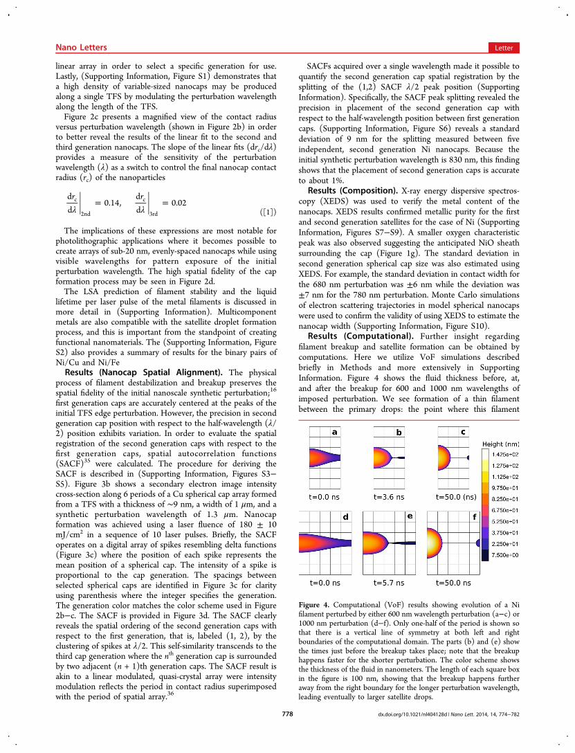
Results (Computational). Further insight regardingfilament breakup and satellite formation can be obtained bycomputations. Here we utilize VoF simulations describedbriefly in Methods and more extensively in SupportingInformation. Figure 4 shows the fluid thickness before, at,and after the breakup for 600 and 1000 nm wavelengths ofimposed perturbation. We see formation of a thin filamentbetween the primary drops: the point where this filament
Figure 4. Computational (VoF) results showing evolution of a Nifilament perturbed by either 600 nm wavelength perturbation (a−c) or1000 nm perturbation (d−f). Only one-half of the period is shown sothat there is a vertical line of symmetry at both left and rightboundaries of the computational domain. The parts (b) and (e) showthe times just before the breakup takes place; note that the breakuphappens faster for the shorter perturbation. The color scheme showsthe thickness of the fluid in nanometers. The length of each square boxin the figure is 100 nm, showing that the breakup happens furtheraway from the right boundary for the longer perturbation wavelength,leading eventually to larger satellite drops.
Nano Letters Letter
dx.doi.org/10.1021/nl404128d | Nano Lett. 2014, 14, 774−782778
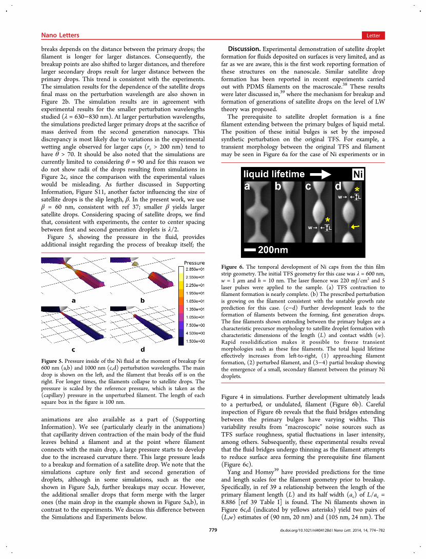
breaks depends on the distance between the primary drops; thefilament is longer for larger distances. Consequently, thebreakup points are also shifted to larger distances, and thereforelarger secondary drops result for larger distance between theprimary drops. This trend is consistent with the experiments.The simulation results for the dependence of the satellite dropsfinal mass on the perturbation wavelength are also shown inFigure 2b. The simulation results are in agreement withexperimental results for the smaller perturbation wavelengthsstudied (λ = 630−830 nm). At larger perturbation wavelengths,the simulations predicted larger primary drops at the sacrifice ofmass derived from the second generation nanocaps. Thisdiscrepancy is most likely due to variations in the experimentalwetting angle observed for larger caps (rc > 200 nm) tend tohave θ > 70. It should be also noted that the simulations arecurrently limited to considering θ = 90 and for this reason wedo not show radii of the drops resulting from simulations inFigure 2c, since the comparison with the experimental valueswould be misleading. As further discussed in SupportingInformation, Figure S11, another factor influencing the size ofsatellite drops is the slip length, β. In the present work, we useβ = 60 nm, consistent with ref 37; smaller β yields largersatellite drops. Considering spacing of satellite drops, we findthat, consistent with experiments, the center to center spacingbetween first and second generation droplets is λ/2.Figure 5, showing the pressure in the fluid, provides
additional insight regarding the process of breakup itself; the
animations are also available as a part of (SupportingInformation). We see (particularly clearly in the animations)that capillarity driven contraction of the main body of the fluidleaves behind a filament and at the point where filamentconnects with the main drop, a large pressure starts to developdue to the increased curvature there. This large pressure leadsto a breakup and formation of a satellite drop. We note that thesimulations capture only first and second generation ofdroplets, although in some simulations, such as the oneshown in Figure 5a,b, further breakups may occur. However,the additional smaller drops that form merge with the largerones (the main drop in the example shown in Figure 5a,b), incontrast to the experiments. We discuss this difference betweenthe Simulations and Experiments below.
Discussion. Experimental demonstration of satellite dropletformation for fluids deposited on surfaces is very limited, and asfar as we are aware, this is the first work reporting formation ofthese structures on the nanoscale. Similar satellite dropformation has been reported in recent experiments carriedout with PDMS filaments on the macroscale.38 These resultswere later discussed in,39 where the mechanism for breakup andformation of generations of satellite drops on the level of LWtheory was proposed.The prerequisite to satellite droplet formation is a fine
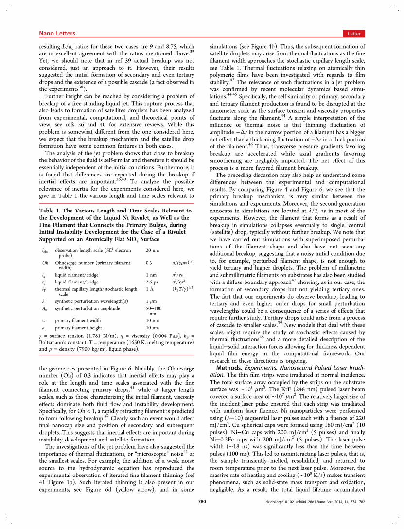
filament extending between the primary bulges of liquid metal.The position of these initial bulges is set by the imposedsynthetic perturbation on the original TFS. For example, atransient morphology between the original TFS and filamentmay be seen in Figure 6a for the case of Ni experiments or in
Figure 4 in simulations. Further development ultimately leadsto a perturbed, or undulated, filament (Figure 6b). Carefulinspection of Figure 6b reveals that the fluid bridges extendingbetween the primary bulges have varying widths. Thisvariability results from “macroscopic” noise sources such asTFS surface roughness, spatial fluctuations in laser intensity,among others. Subsequently, these experimental results revealthat the fluid bridges undergo thinning as the filament attemptsto reduce surface area forming the prerequisite fine filament(Figure 6c).Yang and Homsy39 have provided predictions for the time
and length scales for the filament geometry prior to breakup.Specifically, in ref 39 a relationship between the length of theprimary filament length (L) and its half width (ac) of L/ac =8.886 [ref 39 Table I] is found. The Ni filaments shown inFigure 6c,d (indicated by yellows asterisks) yield two pairs of(L,w) estimates of (90 nm, 20 nm) and (105 nm, 24 nm). The
Figure 5. Pressure inside of the Ni fluid at the moment of breakup for600 nm (a,b) and 1000 nm (c,d) perturbation wavelengths. The maindrop is shown on the left, and the filament that breaks off is on theright. For longer times, the filaments collapse to satellite drops. Thepressure is scaled by the reference pressure, which is taken as the(capillary) pressure in the unperturbed filament. The length of eachsquare box in the figure is 100 nm.
Figure 6. The temporal development of Ni caps from the thin filmstrip geometry. The initial TFS geometry for this case was λ = 600 nm,w = 1 μm and h = 10 nm. The laser fluence was 220 mJ/cm2 and 5laser pulses were applied to the sample. (a) TFS contraction tofilament formation is nearly complete. (b) The prescribed perturbationis growing on the filament consistent with the unstable growth rateprediction for this case. (c−d) Further development leads to theformation of filaments between the forming, first generation drops.The fine filaments shown extending between the primary bulges are acharacteristic precursor morphology to satellite droplet formation withcharacteristic dimensions of the length (L) and contact width (w).Rapid resolidification makes it possible to freeze transientmorphologies such as these fine filaments. The total liquid lifetimeeffectively increases from left-to-right, (1) approaching filamentformation, (2) perturbed filament, and (3−4) partial breakup showingthe emergence of a small, secondary filament between the primary Nidroplets.
Nano Letters Letter
dx.doi.org/10.1021/nl404128d | Nano Lett. 2014, 14, 774−782779
resulting L/ac ratios for these two cases are 9 and 8.75, whichare in excellent agreement with the ratios mentioned above.39
Yet, we should note that in ref 39 actual breakup was notconsidered, just an approach to it. However, their resultssuggested the initial formation of secondary and even tertiarydrops and the existence of a possible cascade (a fact observed inthe experiments38).Further insight can be reached by considering a problem of
breakup of a free-standing liquid jet. This rupture process thatalso leads to formation of satellites droplets has been analyzedfrom experimental, computational, and theoretical points ofview, see refs 26 and 40 for extensive reviews. While thisproblem is somewhat different from the one considered here,we expect that the breakup mechanism and the satellite dropformation have some common features in both cases.The analysis of the jet problem shows that close to breakup
the behavior of the fluid is self-similar and therefore it should beessentially independent of the initial conditions. Furthermore, itis found that differences are expected during the breakup ifinertial effects are important.26,40 To analyze the possiblerelevance of inertia for the experiments considered here, wegive in Table 1 the various length and time scales relevant to
the geometries presented in Figure 6. Notably, the Ohnesorgenumber (Oh) of 0.3 indicates that inertial effects may play arole at the length and time scales associated with the finefilament connecting primary drops,41 while at larger lengthscales, such as those characterizing the initial filament, viscosityeffects dominate both fluid flow and instability development.Specifically, for Oh < 1, a rapidly retracting filament is predictedto form following breakup.42 Clearly such an event would affectfinal nanocap size and position of secondary and subsequentdroplets. This suggests that inertial effects are important duringinstability development and satellite formation.The investigations of the jet problem have also suggested the
importance of thermal fluctuations, or “microscopic” noise41 atthe smallest scales. For example, the addition of a weak noisesource to the hydrodynamic equation has reproduced theexperimental observation of iterated fine filament thinning (ref41 Figure 1b). Such iterated thinning is also present in ourexperiments, see Figure 6d (yellow arrow), and in some
simulations (see Figure 4b). Thus, the subsequent formation ofsatellite droplets may arise from thermal fluctuations as the finefilament width approaches the stochastic capillary length scale,see Table 1. Thermal fluctuations relaxing on atomically thinpolymeric films have been investigated with regards to filmstability.43 The relevance of such fluctuations in a jet problemwas confirmed by recent molecular dynamics based simu-lations.44,45 Specifically, the self-similarity of primary, secondaryand tertiary filament production is found to be disrupted at thenanometer scale as the surface tension and viscosity propertiesfluctuate along the filament.44 A simple interpretation of theinfluence of thermal noise is that thinning fluctuation ofamplitude −Δr in the narrow portion of a filament has a biggernet effect than a thickening fluctuation of +Δr in a thick portionof the filament.46 Thus, transverse pressure gradients favoringbreakup are accelerated while axial gradients favoringsmoothening are negligibly impacted. The net effect of thisprocess is a more favored filament breakup.The preceding discussion may also help us understand some
differences between the experimental and computationalresults. By comparing Figure 4 and Figure 6, we see that theprimary breakup mechanism is very similar between thesimulations and experiments. Moreover, the second generationnanocaps in simulations are located at λ/2, as in most of theexperiments. However, the filament that forms as a result ofbreakup in simulations collapses eventually to single, central(satellite) drop, typically without further breakup. We note thatwe have carried out simulations with superimposed perturba-tions of the filament shape and also have not seen anyadditional breakup, suggesting that a noisy initial condition dueto, for example, perturbed filament shape, is not enough toyield tertiary and higher droplets. The problem of millimetricand submillimetric filaments on substrates has also been studiedwith a diffuse boundary approach47 showing, as in our case, theformation of secondary drops but not yielding tertiary ones.The fact that our experiments do observe breakup, leading totertiary and even higher order drops for small perturbationwavelengths could be a consequence of a series of effects thatrequire further study. Tertiary drops could arise from a processof cascade to smaller scales.39 New models that deal with thesescales might require the study of stochastic effects caused bythermal fluctuations45 and a more detailed description of theliquid−solid interaction forces allowing for thickness dependentliquid film energy in the computational framework. Ourresearch in these directions is ongoing.
Methods. Experiments. Nanosecond Pulsed Laser Irradi-ation. The thin film strips were irradiated at normal incidence.The total surface array occupied by the strips on the substratesurface was ∼105 μm2. The KrF (248 nm) pulsed laser beamcovered a surface area of ∼107 μm2. The relatively larger size ofthe incident laser pulse ensured that each strip was irradiatedwith uniform laser fluence. Ni nanoparticles were performedusing (5−10) sequential laser pulses each with a fluence of 220mJ/cm2. Cu spherical caps were formed using 180 mJ/cm2 (10pulses), Ni−Cu caps with 200 mJ/cm2 (5 pulses) and finallyNi−0.2Fe caps with 200 mJ/cm2 (5 pulses). The laser pulsewidth (∼18 ns) was significantly less than the time betweenpulses (100 ms). This led to noninteracting laser pulses, that is,the sample transiently melted, resolidified, and returned toroom temperature prior to the next laser pulse. Moreover, themassive rate of heating and cooling (∼108 K/s) makes transientphenomena, such as solid-state mass transport and oxidation,negligible. As a result, the total liquid lifetime accumulated
Table 1. The Various Length and Time Scales Relevent tothe Development of the Liquid Ni Rivulet, as Well as theFine Filament that Connects the Primary Bulges, duringInitial Instability Development for the Case of a RivuletSupported on an Atomically Flat SiO2 Surface
lobs observation length scale (SE1 electronprobe)
20 nm
Oh Ohnesorge number (primary filamentwidth)
0.3 η/(γρw)1/2
lη liquid filament/bridge 1 nm η2/γρtη liquid filament/bridge 2.6 ps η3/γρ2
lT thermal capillary length/stochastic lengthscale
1 Å (kBT/γ)1/2
λ synthetic perturbation wavelength(s) 1 μmA0 synthetic perturbation amplitude 50−100
nmw primary filament width 10 nmac primary filament height 10 nm
γ = surface tension (1.781 N/m), η = viscosity (0.004 Pa.s], kB =Boltzmann’s constant, T = temperature (1650 K, melting temperature)and ρ = density (7900 kg/m3, liquid phase).
Nano Letters Letter
dx.doi.org/10.1021/nl404128d | Nano Lett. 2014, 14, 774−782780
using multiple laser pulses leads to the same morphologicalresult as one laser pulse yielding the equivalent liquid lifetime.Simulation results of the time−temperature profile per pulse forthe initially flat Ni film, for example, 26 ns for 6 nm Ni film, areon the order of the predicted breakup times provided by LSA(Figure 2e). These predictions were consistent with the factthat experimentally observed breakup was complete in bothcases after two laser pulses. The details of the time−temperature simulation are presented in ref 16.Nanofabrication (Thin Film Strip Definition). Thin film
strip definition and deposition was accomplished using electronbeam lithography, DC magnetron sputtering, and a solventfacilitated lift-off process, the details of which are provided.28
The Ni thin film strip patterns were exposed into an electronsensitive resist coated on 100 nm SiO2/Si wafers. Specifically, apoly(methyl methacrylate) (PMMA), positive tone electronsensitive resist (495-A4, Shipley) was spin coated using a waferrotation speed of 4000 rpm for a total of 60 s. Following resistapplication, an elevated temperature bake was performed at 180°C using a conventional hot plate. Pattern generation in theresist was performed using a Raith Elphy Quantum softwarepackage that communicated with an FEI Nova 600 dualelectron/ion microscope via a beam blanker. A focused electronprobe with an 18 keV landing energy and 160 pA beam currentwas used to expose the TFS resist patterns. The TFS patternswere exposed using a rectangular scanning grid with a 20 nmexposure step. An exposure dose of 300 μC/cm2 was requiredto yield fully activated TFS patterns for later resist develop-ment. Subsequent resist development was carried out bysubmerging the resist-coated wafer in a solution of 1:3 methylisobutyl ketone (MIBK)/isopropyl alcohol (IPA), respectively,for 100s. An IPA rinse was conducted after removing the waferfrom the MIBK/IPA bath and blown dry with dry N2 gas. Thefinal step in preparation for metal deposition was an oxygenplasma treatment performed in order to remove residual resistfrom the exposed TFS patterns. Specifically, an 8 s exposure ofthe resist-coated wafer to an oxygen plasma generated in areactive ion etcher using a power setting of 100 W to sustain acapacitively coupled plasma. An oxygen flow rate of 10 cm3/min was used with a constant chamber pressure setting of 150mTorr. Regarding metal sputtering, initial thin film stripthicknesses ranged from 6−10 nm for all reported experimentsand are indicated in the appropriate figure captions. In general,sputtering rates of ∼5 nm/min were used to deposit the filmsof Cu, Ni, Ni−0.2Fe, and Cr. The sputtering was conductedusing the DC magnetron method under constant powerdeposition mode at 30 W. A constant chamber pressure of 3mTorr Ar was maintained during sputtering and the target-to-substrate distance was ∼4−5 cm. The Ar gas flow rate was 25cm3/min.Nanofabrication (Chromium Masking and Ion Milling).
These experimental details are provided in SupportingInformation.Energy Dispersive Spectroscopy. These experimental details
are provided in Supporting Information, Figures S7−S9.Simulations. Volume-of-Fluid Simulations. We model the
breakup of the nanostructures by treating the dynamics usingthe two-phase Navier−Stokes equations (Supporting Informa-tion). Briefly, the metal is assumed to be in fluid state for theentirety of the simulation time, ignoring the effects ofsolidification. We perform simulations using a VoF-basedsolver, implemented in an open source software package.48 The
details of this solver are described in ref 49 and some furtherdetails are given in Supporting Information.
■ ASSOCIATED CONTENT*S Supporting InformationDetails related to additional experimental results, imageprocessing and analysis, energy dispersive spectroscopy, andthe volume of fluids simulation method. This material isavailable free of charge via the Internet at http://pubs.acs.org.
■ AUTHOR INFORMATIONCorresponding Author*E-mail: [email protected] authors declare no competing financial interest.
■ ACKNOWLEDGMENTSY.W. and J.D.F. acknowledge support from the U.S. Depart-ment of Energy, Basic Energy Sciences, Materials Science andEngineering Division for sponsoring the aspects of this workrelated to understanding the fundamental mechanismsoperative during liquid phase, thin film dewetting. A portionof this work related to the deposition of thin films andnanolithography was conducted at the Center for NanophaseMaterials Sciences, which is sponsored at Oak Ridge NationalLaboratory by the Scientific User Facilities Division, Office ofBasic Energy Sciences, U.S. Department of Energy. P.D.R.acknowledges support from NSF Grant CBET-1235651. L.K.acknowledges support by NSF Grant CBET-1235710. J.A.D.and A.G.G. acknowledge support from Consejo Nacional deInvestigaciones Cientıficias y Tecnicas (CONICET, Argentina)with Grant PIP 844/2011.
■ REFERENCES(1) Cuenya, B. R. Thin Solid Films 2010, 518 (12), 3127−3150.(2) Billas, I. M. L.; Chatelain, A.; Deheer, W. A. Science 1994, 265(5179), 1682−1684.(3) Zhang, Z.; Li, J. C.; Jiang, Q. J. Phys. D: Appl. Phys. 2000, 33 (20),2653−2656.(4) Alivisatos, A. P. J. Phys. Chem. 1996, 100 (31), 13226−13239.(5) Moshfegh, A. Z. J. Phys. D: Appl. Phys. 2009, 42 (23), 233001.(6) Beliatis, M. J.; Martin, N. A.; Leming, E. J.; Silva, S. R. P.; Henley,S. J. Langmuir 2011, 27 (3), 1241−1244.(7) Atwater, H. A.; Polman, A. Nat. Mater. 2010, 9 (3), 205−213.(8) Pasquale, A. J.; Reinhard, B. M.; Dal Negro, L. ACS Nano 2011, 5(8), 6578−6585.(9) Henzie, J.; Lee, M. H.; Odom, T. W. Nat. Nanotechnol. 2007, 2(9), 549−554.(10) Chou, S. Y.; Krauss, P. R.; Renstrom, P. J. Science 1996, 272(5258), 85−87.(11) Chou, S. Y.; Xia, Q. F. Nat. Nanotechnol. 2008, 3 (6), 369−369.(12) Tan, C.; Peng, C. S.; Pakarinen, J.; Pessa, M.; Petryakov, V. N.;Verevkin, Y. K.; Zhang, J.; Wang, Z.; Olaizola, S. M.; Berthou, T.;Tisserand, S. Nanotechnology 2009, 20 (12), 125303.(13) Ye, J.; Thompson, C. V. Adv. Mater. 2011, 23 (13), 1567−1571.(14) Kumar, G.; Tang, H. X.; Schroers, J. Nature 2009, 457 (7231),868−872.(15) Leong, T. G.; Zarafshar, A. M.; Gracias, D. H. Small 2010, 6 (7),792−806.(16) Fowlkes, J. D.; Kondic, L.; Diez, J.; Wu, Y. Y.; Rack, P. D. NanoLett. 2011, 11 (6), 2478−2485.(17) Xia, Q. F.; Chou, S. Y. Nanotechnology 2009, 20 (28), 285310.(18) Kumar, P. Nano. Res. Lett. 2010, 5 (9), 1367−1376.(19) Henley, S. J.; Carey, J. D.; Silva, S. R. P. Appl. Surf. Sci. 2007, 253(19), 8080−8085.
Nano Letters Letter
dx.doi.org/10.1021/nl404128d | Nano Lett. 2014, 14, 774−782781
(20) Lopes, W. A.; Jaeger, H. M. Nature 2001, 414 (6865), 735−738.(21) Krishna, H.; Shirato, N.; Favazza, C.; Kalyanaraman, R. J. Mat.Res. 2011, 26 (2), 154−169.(22) Henley, S. J.; Beliatis, M. J.; Stolojan, V.; Silva, S. R. P. Nanoscale2013, 5 (3), 1054−1059.(23) Mehrabian, H.; Feng, J. J. J. Fluid Mech. 2013, 717, 281−292.(24) Rayleigh, L. Philos. Mag. Ser. 5 1892, 34 (207), 145−154.(25) Plateau, J. A. F. Acad. Sci. Brux. Mem. 1843, 16, 3.(26) Eggers, J.; Villermaux, E. Rep. Prog. Phys. 2008, 71 (3), 036601.(27) Diez, J. A.; Gonzalez, A. G.; Kondic, L. Phys. Fluids 2009, 21 (8),082105.(28) Fowlkes, J. D.; Kondic, L.; Diez, J. A.; Gonzalez, A. G.; Wu, Y.Y.; Roberts, N. A.; McCold, C. E.; Rack, P. D. Nanoscale 2012, 4 (23),7376−7382.(29) Albella, P.; Garcia-Cueto, B.; Gonzalez, F.; Moreno, F.; Wu, P.C.; Kim, T. H.; Brown, A.; Yang, Y.; Everitt, H. O.; Videen, G. Nano.Lett. 2011, 11 (9), 3531−3537.(30) Kumar, A.; Ciucci, F.; Morozovska, A. N.; Kalinin, S. V.; Jesse, S.Nat. Chem. 2011, 3 (9), 707−713.(31) Valev, V. K.; Silhanek, A. V.; Gillijns, W.; Jeyaram, Y.;Paddubrouskaya, H.; Volodin, A.; Biris, C. G.; Panoiu, N. C.; DeClercq, B.; Ameloot, M.; Aktsipetrov, O. A.; Moshchalkov, V. V.;Verbiest, T. ACS Nano 2011, 5 (1), 91−96.(32) Johnston-Peck, A. C.; Wang, J. W.; Tracy, J. B. ACS Nano 2009,3 (5), 1077−1084.(33) Rathmell, A. R.; Nguyen, M.; Chi, M. F.; Wiley, B. J. Nano. Lett.2012, 12 (6), 3193−3199.(34) Bader, S. D. Rev. Mod. Phys. 2006, 78 (1), 1−15.(35) Pichler, S.; Bodnarchuk, M. I.; Kovalenko, M. V.; Yarema, M.;Springholz, G.; Talapin, D. V.; Heiss, W. ACS Nano 2011, 5 (3),1703−1712.(36) Steurer, W.; Sutter-Widmer, D. J. Phys. D: Appl. Phys. 2007, 40(13), R229−R247.(37) Roberts, N. A.; Fowlkes, J. D.; Mahady, K.; Afkhami, S.; Kondic,L.; Rack, P. D. ACS Appl. Mater. Interfaces 2013, 5 (10), 4450−4456.(38) Gonzalez, A. G.; Diez, J.; Gratton, R.; Gomba, J. Europhys. Lett.2007, 77, 44001.(39) Yang, L.; Homsy, G. M. Phys. Fluids 2007, 19 (4), 044101.(40) Eggers, J. Rev. Mod. Phys. 1997, 69 (3), 865−929.(41) Brenner, M. P.; Shi, X. D.; Nagel, S. R. Phys. Rev. Lett. 1994, 73(25), 3391−3394.(42) Castrejon-Pita, A. A.; Castrejon-Pita, J. R.; Hutchings, I. M. Phys.Rev. Lett. 2012, 108 (7), 074506.(43) Willis, A. M.; Freund, J. B. Phys. Fluids 2010, 22 (2), 022002.(44) Moseler, M.; Landman, U. Science 2000, 289 (5482), 1165−1169.(45) Fowlkes, J.; Horton, S.; Fuentes-Cabrera, M.; Rack, P. D. Angew.Chem., Int. Ed. 2012, 51 (35), 8768−8772.(46) Eggers, J. Phys. Rev. Lett. 2002, 89 (8), 084502.(47) Ghigliotti, G.; Zhou, C.; Feng, J. J. Phys. Fluids 2013, 25 (7),072102.(48) Popinet, S. http://gfs.sourceforge.net/wiki/index.php/Main_Page, 2012, 1.3.2.(49) Popinet, S. J. Comput. Phys. 2009, 228 (16), 5838−5866.
Nano Letters Letter
dx.doi.org/10.1021/nl404128d | Nano Lett. 2014, 14, 774−782782