Embed Size (px)
Citation preview

AD-A27 5 519
DTICFEB 7 19'94 ,
FINAL REPORT
Interconnections in ULSI: Correlation and Crosstalk
Gary H. Bernstein, Supriyo Bandyopadhyay, and Wolfgang Porod
Department of Electrical Engineering
University of Notre Dame
Notre Dame, IN 46556
Final Report for Period 1 January 1991 - 31 December 1992
ONR Grant Number: N00014-91-J-1505
R&T Number: 4145391 --- 02
94-04110
Submitted to
Office of Naval Research, Electronics Division
Arlington, VA 22217
04 2 04 108

Intemonnections in ULSI: Correlation and Crossialk
Summary of Research
During the period 1 January 1991 to 31 December 1992, research supported by the Office ofNaval Research under Grant Number N00014-91-J-1505 was directed at studying the phenomenaof correlation and crosstalk in future ULSI interconnects. As described in the body of this reportthe coupling phenomena include: (i) line - line coupling, (ii) dot - dot coupling, and (iii) line - dotcoupling. We have also addressed the photovoltaic effect, which leads to an induced voltage in aline due to electromagnetic radiation which may be caused by neighboring lines. We also discussrelated issues of the fabrication and design of quantum wire and dot structures.
The research supported by the present grant resulted in 36 refereed journal papers and 49 confer-ence publications and presentations. Graduate student support led, in part, to 5 M.S. theses andone Ph.D. dissertation. Individuals whose research was supported, in part, by the present fundsinclude Gary H. Bernstein, S. Bandyopadhyay, Wolfgang Porod, and graduate students SureshSubramaniam, Nina Telang, Xiaokang Huang, Greg Bazan, and Henry Harbury.
DTiC QUALITY TNSPECTI!7D 5
Accesion For
NTIS CRA&ID0IC TAB C
4 t 1' ." o
[ t
Summary of Research 2
Interconnections in ULSI: Correlation and Crosstalk
Line - Line Coupling
Fabrication of dense interconnect structuresInvestigator: G. H. Bernstein
The central mechanism for current drag between metal interconnects is expected to be Coulombmutual scattering. However, since screening is very strong in metals, in order to observe possiblecurrent drag phenomena between metal interconnects, metal patterns must be extremely small andplaced very closely together- about 10 nm lines and spaces. Our continued work on high contrastelectron resist developers proved critical to the success of achieving the highest possible litho-graphic resolution.
To this end, we have studied extensively the technology for creating such structures withoutresorting to such techniques as shadow evaporation. Direct fabrication of such patterns is necessi-tated by the need to make connections to the individual lines through which currents are sent andmeasured. Our basic tool is electron beam lithography of poly (methyl methacrylate) (PMMA).The two central issues to creating very dense patterns as described above are proximity effectsand the strength of PMMA "walls".
Proximity effects are important since the lines are so closely spaced that electron scattering phe-nomena enter a new regime not commonly studied for the fabrication of conventional integratedcircuits. Most proximity effect studies use a double Gaussian model taking into account shortrange forward scattering and long range backscattering. Usually not considered, however, are thehigh energy secondary electrons of intermediate range. We performed a very careful study fittingcurves to include a third Gaussian component due to the fast secondary electrons. Figure 1 showsthe relative dose necessary to create lines of equal width as a function of the grating pitch. It wasfound that the use of the third, intermediate range, component gave a much better fit to the datathan the use of only two Gaussian components. We believe this is the only study to date of theproximity effect on the size scales of a few tens of nm.
1.2t
o 00• 0 ..... u.. ..........--
•. .. -,-• .-.. 0 - , ....... ,... ... .. .. .. ... .. .. ..
S0.91-0
S0.8 X, 0, + Experimental data0.7
o ° ......... Only forward electrons
S . Double Gaussian model
Z 0.6 ....... Triple Gaussian model
0.5-
0.40 0.05 0.1 0.15 0.2 0.25 0.3 0.35
Pitch of Gratings (jim)
Fig. I: Normalized dose for equal line widths as a function of grating pitch. The agreement with atriple Gaussian model shows that fast secondary electrons play a significant role in the exposure.
Line - Line Coupling 3

Interconnections in ULSI: Correlation and Crosstalk
The strength of PMMA walls is important because the spacing of the lines is much smaller thanthe thickness of the starting resist. When the (positive) resist is developed out to form the lines bylift-off, a wall of PMMA remains to form the space between the two lines. Since the length of thewalls is very long (on the order of 50 to 100 microns), the walls have a tendency to wave andbuckle under the stress of the development process, whereas very straight walls are necessary forthe experiments. This phenomenon required a very good understanding of the forces in order tocontrol the process for the continuation of the current drag experiments. We found that the lack ofstability was due not to process control or technique, but rather to the very slight swelling of thePMMA with the developer leading to buckling of the walls. Furthermore, grating structures had atendency to fail in very regular arrays of waves which seemed at first to be due to either noise onthe electron beam or poor development/drying procedures. Our study revealed that the regularpatterns were in fact due to attractive forces through the developer fluid which set up a pattern ofwall failure across the grating.
One new and interesting outcome of the study was the role of swelling in the development ofPMMA. It was universally believed that a contributing factor to the ultra-high resolution proper-ties of PMMA was the absence of any swelling characteristics. We found that in the regime ofnarrow walls, the very slight swelling that does exist as a consequence of the normal chemicaldevelopment sequence of events does indeed impact the results on this size scale.
A directly applicable result of the study was the relationship that the fabrication of reliablystraight walls is achieved under the condition of not exceeding a ratio of wall height to thicknessof 5. This applies over a wide range of starting resist thicknesses. Using insights gained from thestudy, we were able to fabricate gold gratings of thickness 15 nm with pitch as small as 38 nm(Fig. 2) and gold line pairs on a pitch of 36 nm. To our knowledge, these are the densest patternsever fabricated using direct lithographic techniques.
Fig. 2: Ti/Au (2 nm/15 nm) grating with 38 nm pitch fabricated by electron beam lithography using
our high contrast developer.
Line - Line Coupling 4

Interconnections in ULSI: Correlation and Crosstalk
Relevant Publications:
G. H. Bernstein, D. A. Hill and W. P. Liu, "New High-Contrast Developers for PMMA Resist,"Journal of Applied Physics 71, 4066 - 4075 (1992).
G. H. Bernstein and D. A. Hill, "On the Attainment of Optimum Development Parameters forPMMA Resist," Superlattices and Microstructures 11, 237-240 (1992).
X. Huang, G. Bazan, G. H. Bernstein, and D. A. Hill, "Stability of Thin Resist Walls," Journal ofthe Electrochemical Society 139, 2952-2956 (1992).
D. A. Hill, X. Huang, G. Bazan, and G. H. Bernstein, "Swelling and Surface Forces-InducedInstabilities in Nanoscopic Polymeric Structures," Journal of Applied Physics 72, 4088-4094(1992).
X. Huang, G. H. Bernstein, G. Bazan, and D. A. Hill, "Spatial Density of Lines in PMMA byElectron Beam Lithography," Journal of Vacuum Science and Technology A 11, 1739-1744(1993).
X. Huang, G. Bazan, G. H. Bernstein, "New Technique for Computation and Challenges for Elec-tron Beam Lithography," Journal of Vacuum Science and Technology B 11, 2665 - 2569 (1993).
Experimental Study of Coupling between Metal LinesInvestigator: G. H. Bernstein
In order to increase confidence in our low temperature measurement techniques, we replicatedpreviously published work by other groups in which the length dependence of universal conduc-tance fluctuations in 1-D structures was investigated. Figure 3 shows the dependence of the mag-nitude of the conductance fluctuations on the length of gold wires with cross-sections of 30 nm by70 nm at 1.8K. The existence of an Un dependence (where n=1.5 to 2) is characteristic of thisphenomenon, and is in agreement with the previous experiments.
010-
0
0 0
0.1
0.01* . . . . .
0.1 1 10
L/L#
Fig. 3: Magnitude of the conductance fluctuations as a function of wire length.
Line - Line Coupling 5

Interconnections in ULSI: Correlation and Crossuak
Having established the credibility of our measurement set-up, we proceeded to measure currentdrag in normal metal wires. In this phase of the research effort, six attempts over six months weremade at finding current drag between gold lines at 1.7K to 4.2K with linewidths of 50 nm andspaces of 25 nm. The decision to use linewidths larger than those discussed above was based onmeasurement issues. The ratio of current drag to drive current reported in the literature was on theorder of 10-5, and drive currents needed to be about 100 nA, putting the drag current into the pArange. In our case, we expected a considerably lower drag/drive current ratio, and did not wish togo below 10 microamps for the drive current, with the ability to measure down to 1 pA (10,7ratio). Thinner lines than those used would not have withstood such large drive currents.
In the course of the experiment, considerable progress was made in improving the measurementsystem to 0.1 pA measurements and eliminating all sources of stray cross-talk between measure-ment lines, but no evidence was seen of actual coupling between the lines on chip. We believe thatthe reason for failure is that we had not succeeded in meeting the specifications for the patternsand measurements as outlined above. Beyond 10 nm linewidths, the screening was likely so largethat any Coulomb effects directed from the drive to the drag lines were screened near the surfaceof the drag line, so that most of the electrons in the drag line were unaffected by the Coulombicfields induced by the drive electrons, and very little momentum transfer resulted. Given bettermeasurement techniques now implemented, we will revisit this regime and look for possibleeffects.
Through extensive discussions with Dr. N. Giordano at Purdue University, we decided to pursuethe work in the area of superconducting films and lines. The basis for this decision was the expec-tation that the Cooper pairs involved in the phenomenon of superconductivity enjoy very longcoherence lengths - on the order of several tens of nm. Because of this, screening of the charge-induced momentum transfer will be much less, and therefore is expected to survive on the sizescales used in the experiment.
Although he has not observed coupling between normal metal (NM) films, Giordano has alreadyobserved drag between thin films of NM and superconducting (SC) metals [private comm.,unpublished]. His work showed that current drag developed within the NM and SC temperaturetransition regime. For this reason, he (and we) chose a material that has a wide transition temper-ature range so that the crossover from no drag to drag can be more easily studied. We chose alu-minum/oxygen compounds which shift the critical temperature of aluminum from 1.2K to as highas 1.95K with a transition range of about 0.1K.
By introducing oxygen during aluminum evaporation, we have succeeded in achieving films witha wide range of transition temperatures. Using these films, we have observed current dragbetween films. Figure 4 shows induced voltage in the SC film due to current driven through a goldfilm. Both films are 20 nm thick, separated by 35 nm of A120 3 (insulating). The coupling occursonly in the temperature range over which the SC film changes from normal to SC (solid line in thefigure). It is interesting that the induced voltage decreases as the resistance of the SC filmapproaches zero, i.e. purely superconducting (also observed by Giordano). We believe this is dueto the nature of the SC material i.e. a superconductor cannot support a voltage drop. As the tem-perature decreases and electrons pair up, the coherence length grows and coupling begins. How-ever, as pairing is completed, there is a canceling of the voltage due to the coupling and thesuperconductivity, so the voltage decreases to zero as it must in a SC.
Line - Line Coupling 6

Interconnections in ULSI: Correlation and Crosstalk
0.3
0.2
. 0.1 Resist= (WOO k~oh/m/
o -0.0U
>-0.1
04.0.2 Induced Voltage(xlOO nV)
-0.3 %I , I , I i I I
1.85 1.90 1.96 2.00 2.05
T(K)
Fig. 4: Induced voltage in the superconducting film due to current driven through a gold film.
Work is continuing in order to observe coupling between NM and SC lines. We plan to pursueseveral schemes for current drag between lines including lines lying side-by-side and over eachother. There are advantages to both schemes which is the subject of the dissertation of XiaokangHuang. Both schemes will rely heavily on our ability to perform very accurate alignmentsbetween metal levels (see the section on Dot-Dot Coupling).
Theory of Line -Line CouplingInvestigator: S. B andyopadhyay
A general theoretical framework was developed for studying coupling and crosstalk betweenultranarrow and ultradense interconnects in ULSI. Both coupling between optical interconnectsand quantum mechanical coupling between silicide interconnects were studied using this theory.It was found that generic optical interconnects are quite immune to crosstalk since GaAs/A1GaAsoptical waveguides (interconnects) are non-leaky. In contrast, quantum mechanical tunnelingbetween contiguous closely spaced silicide lines can be quite significant if the lines are about 5nm apart. To suppress this coupling, a possible remedy is to dust the intervening dielectric withmagnetic impurities which are known to inhibit tunneling. A paper describing this research waspublished in the IEEE Journal of Quantum Electronics (provided in the appendix).
Relevant Publications:
S. Bandyopadhyay, "Coupling and Crosstalk Between High Speed Interconnects in Ultra LargeScale Integrated Circuits," IEEE Journal of Quantwn Electronics 28, 1554 - 1561 (1992).
Line - Line Coupling 7

Inteaconnections in ULSI: Correlation and Crosstalk
Line - Line Coupling by Phonon-Assisted Hopping of ElectronsInvestigator: S. Bandyopadhyay
A possible source of coupling between narrow contiguous wires is phonon assisted hopping ofelectrons from one wire to another. In addition to crosstalk, this kind of events can also cause Shotnoise in the interconnects. We have calculated phonon scattering rates in quantum wires and atpresent are investigating phonon assisted hopping rates. We have also found that a magnetic fieldcan dramatically suppress acoustic phonon emision in quantum wires. This also has very seriousimplications for the quantum Hall effect in one-dimensional systems. Several papers describingthe effect of a magnetic field on phonon scattering have been published.
Relevant Publications:
N. Telang and S. Bandyopadhyay, "Quenching of Acoustic Phonon Scattering of Electrons inSemiconductor Quantum Wires Induced by a Magnetic Field," Applied Physics Letters 62,3161 (1993).
N. Telang and S. Bandyopadhyay, "'Modulation of Electron Phonon Scattering in Quantum Wiresby a Magnetic Field," Semiconductor Science and Technology (in press).
N. Telang and S. Bandyopadhyay, "The Effect of a Magnetic Field on Polar Optical and SurfacePhonon Scattering Rates," Physical Review B 48 (Dec 15 - 1993).
Magnetotransport in Quantum WiresInvestigator: S. Bandyopadhyay
A formalism was developed for calculating the electron wavefunction and the energy dispersionrelation of hybrid magnetoelectric states in ultranarrow quantum wires in the presence of a mag-netic field. The results are exact solutions of the Schrtdinger equation. The importance of thiswork is that it allows one to study the effect of a magnetic field on transport in narrow quasi-onedimensional wires. We are extending this work is to study transport in two coupled wires. Atpresent, we are studying the following problem. An electron is introduced into a wire at a certaininstance of time. We would like to find out after what time the electron switches over to an adjoin-ing wire and with what efficiency. This requires solving the time dependent Schr6dinger equation,for which we have formulated a general prescription that is valid even in the presence of a mag-netic field. A paper describing the first (steady-state) part of this work was published in the Jour-nal of Applied Physics (provided in the appendix).
Relevant Publications:
S. Chaudhuri and S. Bandyopadhyay, "Numerical Calculation of Hybrid Magnetoelectric Statesin an Electron Waveguide, Journal of Applied Physics 71, 3027 - 3029 (1992).
Line - Line Coupling 8
Interconnections in ULSI: Correlation and Crosstalk
Spatial Current Distribution in Quantum WiresInvestigator: S. Bandyopadhyay and W. Porod
A formalism was developed for studying the spatial distributions of the current, potential, excesscarrier concentration, residual resistivity dipoles and electromigration forces in quantum wires ina magnetic field. A paper describing these results was published in Superlattices and Microstruc-tures. It was also presented at the Sixth International Conference on Superlattices, Microstruc-tures and Microdevices, Beijing, People's Republic of China, August, 1992. A more detailedversion of this paper appeared in Physical Review B (provided in the appendix).
In addition, we have also obtained self-consistent electronic states through an iterative solution ofthe 2-D Schridinger equation using current carrying boundary conditions. Any bound electroniccharge is approximated by the semi-classical Thomas-Fermi screening model. The Hartree poten-tial due to the electron density is explicitly determined from the total charge density in each itera-tion, and is used to calculate the electronic states in the subsequent iteration. The self-consistentsolution is obtained when the potential difference between iterations converges to within a desiredtolerance. The results of this work are described in a paper in Superlanices and Microstructures.
Relevant Publications:
Henry K. Harbury, Wolfgang Porod, and Craig S. Lent, "Field Effects in Self-Consistent Trans-port Calculations for Narrow Split-Gate Structures," Superlattices and Microstructures 11, 189- 193 (1992).
S. Chaudhuri and S. Bandyopadhyay, "Quantum Transport in a Disordered Quantum Wire in thePresence of a Magnetic Field," Superlanices and Microstructures 11, 241 - 244 (1992).
S. Chaudhuri and S. Bandyopadhyay, "Spatial Distribution of the Current and Fermi CarriersAround Localized Elastic Scatterers in Quantum Transport," Physical Review B 45, 11126 -11135 (1992).
S. Bandyopadhyay, S. Chaudhuri, B. Das, and M. Cahay, "Features of quantum magnetotransportand electromigration in mesoscopic systems," Superlanices and Microstructures 12, 123 - 132(1992).
S. Chaudhuri, S. Bandyopadhyay, and M. Cahay, "Spatial distribution of the current, Fermi carrierdensity, potential and electric field in a disordered quantum wire in a magnetic field," PhysicalReview B 47, 12649 (1993).
Design of Quantum Wires at Corrugated HeterointerfacesInvestigator: W. Porod
in collaboration with Dr. S. M. Goodnick (OSU)
We have investigated the formation of a quantum wire structure by the confinement of electronsbetween lateral quasi-two-dimensional p-n junctions at corrugated GaAs/AlGaAs heterostruc-tures. Such a quantum wire may be realized at the tip of a Si-doped A1GaAs overgrown V groovein a SI-GaAs substrate due to the surface orientation dependence of Si doping. The two-dimen-sional conduction and valence band profiles for the electron and hole charge densities are
Line - Line Coupling 9
Inteaconnections in ULSI: Correlation and Crosstalk
obtained numerically within a semiclassical Thomas-Fermi screening model. The quantized elec-tronic wire states at the heterointerface are then obtained by solving the two-dimensional effectivemass Schr6dinger equation using the calculated potential profile. We have explored the parameterspace of the one-dimensional electronic system and we established which features of the structureare dominant factors in controlling the quantum confinement. Specifically, we found that theenergy level spacing of the quantum wire depends primarily upon the lateral confinement width inthe n-type region at the tip of the V groove. The ground state energy of the wire is shown todepend on both the lateral confinement width and the vertical heterointerface confinement width.We have also studied the effect of lateral gates on the side walls of the V groove in order to obtaindirect control of the quantum wire transport properties. Our studies have resulted in an experi-mental effort in the group of Dr. Jim Merz at UC Santa Barbara, which is aimed at realizing sucha quantum wire structure by MBE techniques.
Relevant Publications:
Henry K. Harbury, Wolfgang Porod, and Stephen M. Goodnick, "Lateral p-n junctions betweenquasi two-dimensional electron and hole systems at corrugated GaAs/A1GaAs interfaces,"Journal of Vacuum Science and Technology B 10, 2051 - 2055 (1992).
Wolfgang Porod, Henry K. Harbury, and Stephen M. Goodnick, "Lateral p-n junctions and quan-tum wires formed by quasi two-dimensional electron and hole systems at corrugated GaAs/AlGaAs interfaces," Applied Physics Letters 61, 1823 - 1825 (1992).
Henry K. Harbury, Wolfgang Porod, and Stephen M. Goodnick, "A Novel Quantum Wire Formedby Lateral p-n-p Junctions Between Quasi-Two-Dimensional Electron and Hole Systems atCorrugated GaAs/AlGaAs Interfaces," Journal of Applied Physics 73, 1509 - 1520 (1993).
Line - Line Coupling 10
Interconnections in ULSL: Correlation and Crosstalk
ot - Dot Coupling
abrication of dense dot arrays| Investigator: G. H. Bernstein
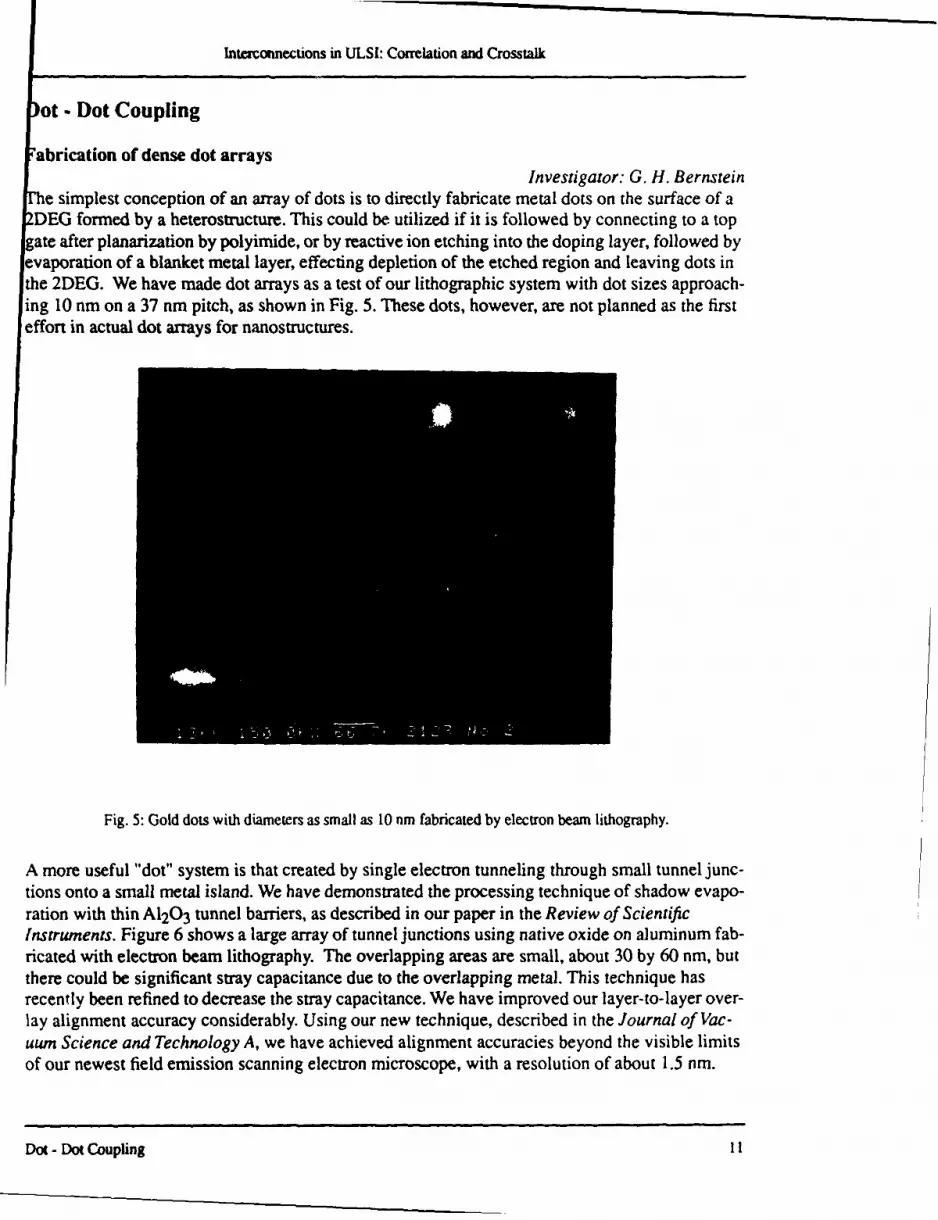
e simplest conception of an array of dots is to directly fabricate metal dots on the surface of aDEG formed by a heterostructure. This could be. utilized if it is followed by connecting to a top
gate after planarization by polyimide, or by reactive ion etching into the doping layer, followed byevaporation of a blanket metal layer, effecting depletion of the etched region and leaving dots inthe 2DEG. We have made dot arrays as a test of our lithographic system with dot sizes approach-ing 10 nm on a 37 nm pitch, as shown in Fig. 5. These dots, however, are not planned as the firsteffort in actual dot arrays for nanostructures.
Fig. 5: Gold dots with diameters as small as 10 nm fabricated by electron beam lithography.
A more useful "dot" system is that created by single electron tunneling through small tunnel junc-tions onto a small metal island. We have demonstrated the processing technique of shadow evapo-ration with thin A120 3 tunnel barriers, as described in our paper in the Review of ScientificInstruments. Figure 6 shows a large array of tunnel junctions using native oxide on aluminum fab-ricated with electron beam lithography. The overlapping areas are small, about 30 by 60 nm, butthere could be significant stray capacitance due to the overlapping metal. This technique hasrecently been refined to decrease the stray capacitance. We have improved our layer-to-layer over-lay alignment accuracy considerably. Using our new technique, described in the Journal of Vac-uum Science and Technology A, we have achieved alignment accuracies beyond the visible limitsof our newest field emission scanning electron microscope, with a resolution of about 1.5 nm.
Dot - Dot Coupling 1

Interconnections in ULSI: Correlation and Crosstalk
Fig. 6: Array of tunnel junctions fabricated by shadow evaporation.
Figure 7 shows a tunnel junction fabricated by the alignment of one metal line against another onsubsequent processing and metalization steps. The alignment is so accurate that no horizontal off-set can be seen at 250,000 times magnification. Overlap in the vertical direction exists onlybecause of proximity effect elongation of the lines beyond their actual lithographic placement, sothat with the two lines combined, an extremely small tunnel junction has resulted with an area ofabout 30 by 30 nm2 . We plan to test devices of this quality in the near future.
Fig. 7: Very small overlap of two wires to be used as a single electron tunnel junction. The wireswere placed over each other by a nearly perfect alignment of two metal layers.
Dot - Dot Coupling 2

Interconnections in ULSI: Correlation and Crosstalk
Relevant Publications:
S. J. Koester, G. Bazan, G. H. Bernstein, and W. Porod, "Fabrication of Ultrasmall Tunnel Junc-tions by Electron Beam Lithography," Review of Scientific Instruments 63, 1918 - 1921 (1992).
G. Bazan and G. H. Bernstein, "Electron Beam Lithography Over Very Large Scan Fields," Jour-nal of Vacuun Science and Technology A 11, 1745-1752 (1993).
Physical Coupling between Quantum Dots for Cellular Automata ArchitecturesInvestigators: W Porod and G. H. Bernstein
in collaboration with Dr. C. S. Lent
We have studied architectures composed of quantum structures which are based on the physicalcoupling between the individual elements. We have pursued the general notion of computing ingranular arrays of quantum dots, similar to cellular automata. In a specific example, we haveimplemented cellular automata rules which correspond to a solution of the Helmholtz equation.Our simulations exhibited wave behavior, such as Huygen's principle, interference, and diffirac-tion at a slit. We have attempted to employ these wave phenomena to computing on a chip, butmore work is needed.
Perhaps our most successful avenue of research was aimed at developing a specific model systemfor the coupling between quantum dots. In these so-called quantum cellular automata, each cell iscomposed of several quantum dots which are occupied by only a few electrons. Inside each cell,electrons my tunnel from one dot to the next. No tunneling is allowed between cells. Electrons,both within and between cells, interact Coulombically. We have demonstrated bistable behaviorof the charge alignment in each cell, which is due to intracellular quantum mechanics and inter-cellular Coulomb coupling. This bistability is akin to gain and saturation in conventional electron-ics. In ongoing work, computing elements have been demonstrated, building upon the basicquantum cell.
This work has led to a new project, which is entitled "Quantum Cellular Automata," and which issponsored by ARPA and administered by ONR.
Relevant Publications:
Craig S. Lent, P. Douglas Tougaw, and Wolfgang Porod, "Bistable saturation in coupled quantumdots for quantum cellular automata," Applied Physics Letters 62, 714 - 716 (1993).
Craig S. Lent, P. Douglas Tougaw, Wolfgang Porod, and Gary H. Bernstein, "Quantum CellularAutomata," Nanotechnology 4, 59 - 57 (1993).
P. Douglas Tougaw, Craig S. Lent, and Wolfgang Porod, "Bistable Saturation in Coupled Quan-tum-Dot Cells," Journal ofApplied Physics 74, 3558 - 3566 (1993).
Numerical modelling of quantum dot structuresInvestigator: W. Porod
Knowledge of the potential profiles in quantum dot structures is an important issue both for the
Dot - Dot Coupling 13

Interconnections in ULSI: Correlation and Crosstalk
design of quantum dots as well as for a study of dot - dot coupling. We have developed a numeri-cal technique which allows us to model the effect of close-by surface states and the interface tothe dielectric. Specifically, we have studied potential distributions and quantized electronic statesin gated AlGaAs/GaAs quantum dot structures obtained from self-consistent solutions of the axi-symmetric Poisson and Schr6dinger equations. Our model takes into account the effect of surfacestates by viewing the exposed surface as the interface between the semiconductor and the dielec-tric. We investigate the occupation of the quantum dot structures as a function of (i) gate bias, (ii)distance of the confining heterointerface from the top gate, and (iii) different physical models ofthe interface charge at the exposed semiconductor surface. This modelling is important for thedesign of our recently proposed mesoscopic computing architectures, called Quantum CellularAutomata, which consist of arrays of interacting quantum dot cells occupied by few electrons.
Relevant Publications:
Minhan Chen, Wolfgang Porod, and David J. Kirkner, "A Coupled Finite Element/Boundary Ele-ment Method for Semiconductor Quantum Devices with Exposed Surfaces," Journal of AppliedPhysics 75 (Mar 1 - 1994).
Supercomputing with spin polarized single electronsInvestigator: S. Bandyopadhyay,
in collaboration with Drs.Miller and Das
We have proposed a novel quantum technology for ultrafast, ultradense and ultra-low powersupercomputing. The technology utilizes single electrons as binary logic devices in which the spinof the electron encodes the bit information. The architecture mimics quantum coupled two dimen-sional cellular automata without physical interconnects. It is realized by laying out on a wafer reg-imented arrays of nanophase particles each hosting an electron. Various types of logic gates,combinational circuits for arithmetic logic units, and sequential circuits for memory can be real-ized. The technology has many advantages such as (1) the absence of physical interconnectsbetween devices (inter-device interaction is provided by quantum mechanical coupling betweenadjacent electrons), (b) ultrafast switching times of about 1 picosecond for individual devices, (c)extremely high bit density approaching 10 Terabits/cm 2, (4) non-volatile memory, (5) robustnessand possible room temperature operation with very high noise margin and reliability, (6) a verylow power delay product for switching a single bit (about 10-20 Joules), and (7) a very smallpower dissipation of a few tens of nanowatts per bit.
We are also investigating possible routes of clocking this type of a chip with coherent electromag-netic radiation that can induce magnetic dipole transitions. This is the closest realization of theBenioff-Zurek-Peres type quantum spin computer for dissipationless computation as envisaged byFeynman. We have found that the Hamiltonian of the system (including the radiation) can be Her-mitean so that the computation represented by the transformation exp[-2ni Ht /h] is unitary. Weare presently studying the time evolution of such a system. Finally, we have proposed a novel fab-rication technology for producing single electron chips that involves selective area nucleation ofnanophase particles. This work is being carried out in collaboration with Argonne National Labo-ratory and the National Institute of Standards and Technology, Gaithersburg, Maryland.
Dot - Dot Coupling 14
Interconnections in ULSI: Correlation and Crosstalk
Line - Dot Coupling
Investigator: W. Porodin collaboration with Dr. C. S. Lent
Line-to-dot coupling will be utilized in our proposed Quantum Cellular Automata architectures tosense the polarization of a particular cell. In other words, this phenomenon will serve as theREAD operation. Line - dot coupling may also be used to set the initial state of an array of quan-tum dot cells.
So far, we have studied transmission phenomena when coupling a quantum waveguide to a reso-nator, which may be realized as a quantum dot. In particular, we have investigated the propertiesof the transmission amplitude in the complex-energy plane. We find that, similar to double-barrierresonant tunneling, there are transmission poles in the complex-energy plane for quantumwaveguide structures which contain quasi-bound states in attached t-stub resonators. In contrast todouble-barrier resonant tunneling, however, we also find that the quantum wire networks alsopossess transmission zeros (antiresonances), which always occur on the real-energy axis. Theexistence of transmission zeros is a characteristic feature of quantum waveguide system withattached resonators, but is absent for double-barrier resonant tunneling, which contains the reso-nant cavity as part of the transmission channel. We demonstrate that each quasi-bound state of theresonantly-coupled quantum waveguide system leads to a zero-pole pair of the transmissionamplitude in the complex-energy plane. The previously noted resonance - antiresonance behaviorof the transmission probability, which leads to its sharp variation as a function of energy, can beunderstood in terms of these zero-pole pairs.
We have also investigated the line shape of the transmission probability in quantum waveguideswith resonantly-coupled cavities. Resonance/antiresonance features in the vicinity of each quasi-bound state can be characterized by a zero-pole pair in the complex-energy plane, which leads toasymmetrical transmission peaks. We have found a generalization of the familiar symmetricalLorentzian line. Using several examples, we demonstrate the utility of our proposed line shape toextract the lifetime of the quasi-bound state by a fit to the data. We also discuss the asymmetricalline shapes in the context of Fano resonances.
Relevant Publications:
Wolfgang Porod, Zhi-an Shao, and Craig S. Lent, "Transmission Resonances and Zeros in Quan-tum Waveguides with Resonantly-Coupled Cavities," Applied Physics Letters 61, 1350 - 1352(1992).
Wolfgang Porod, Zhi-an Shao, and Craig S. Lent, "Resonance-Antiresonance Line Shape forTransmission in Quantum Waveguides with Resonantly-Coupled Cavities," Physical Review B48,8495 - 8498 (1993).
Zhi-an Shao, Wolfgang Porod, and Craig S. Lent, "Transmission Resonances and Zeros in Quan-tum Waveguide Systems with Attached Resonators," Physical Review B (in press).
Line - Dot Coupling 15

Interconnections in ULSI: Correlation and Crosstalk
Photovoltaic Effect in the Presence of Magnetic Fields
Investigator: G. H. Bernsteinin collaboration with Dr. N. Giordano (Purdue)
From a practical point of view, metal interconnects used in mesoscopic systems will be subject tosome electrical noise and interference. Since circuits utilizing mesoscopic phenomena will oper-ate at frequencies high in the microwave range, we must be concerned with the effects of micro-wave bombardment and current drive on mesoscopic systems. Of a scientific interest, theexistence of photovoltages induced by bombardment of microwave radiation (the photovoltaic(PV) effect) has proved fertile ground for studying the interaction of high frequency electric fieldson conduction electrons in metals. One present model for the PV effect is that electrons absorbmicrowave photons, and being out of equilibrium with the Fermi sea, the energetic electrons dif-fuse in a direction preferential to the precise impurity distribution. Because of this, a DC voltageon the order of nV develops across the leads of the device.
We have engaged in an extensive collaboration with Dr. Giordano and graduate student R. Bartoloto study the photovoltaic effect in mesoscopic structures. Prior to our involvement, their work wasconfined to structures with dimensions of about one micron. We have collaborated to produce avariety of structures with dimensions to 50 nm in the form of wires and rings of diameter 330 to500 nm, measured at Purdue University.
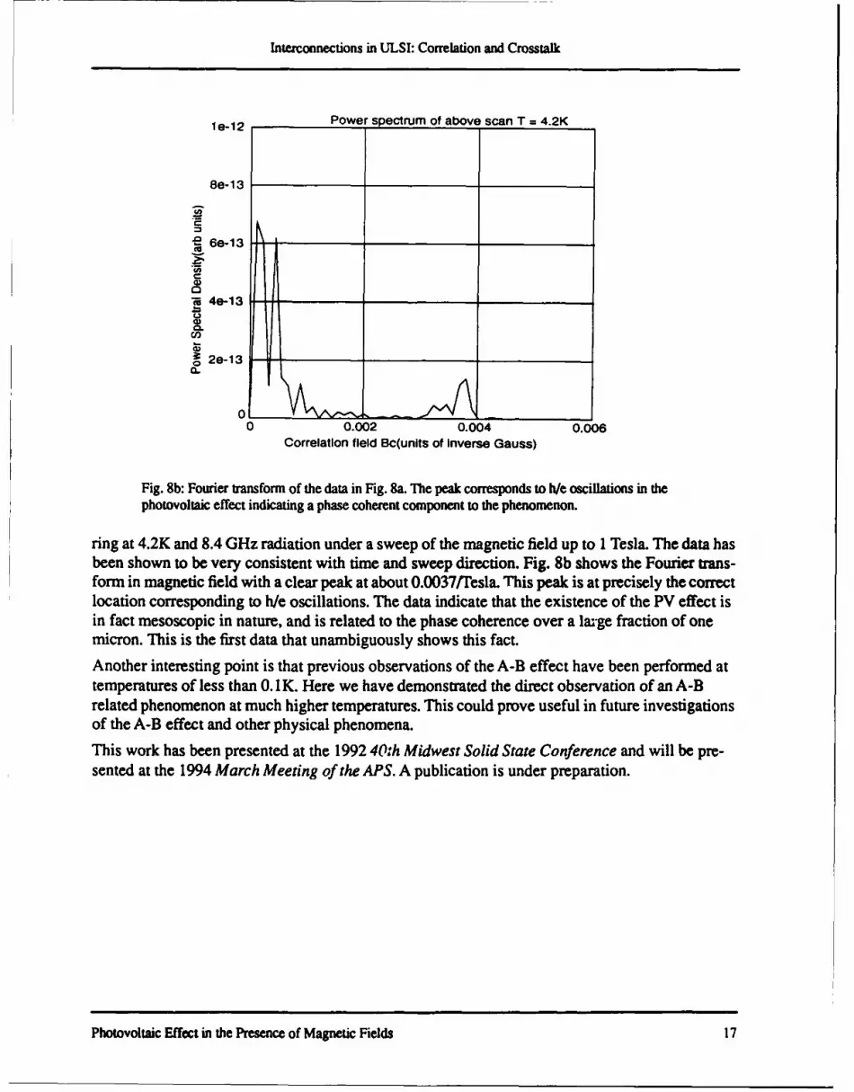
We have fabricated (on glass substrates) gold 1-D wires with widths of 50 to 70 nm, thicknessesof 20 nm, and total lengths of up to 1.5 microns. These structures clearly showed evidence of thePV effect at 4.2K. Although the results from the small wires were essentially the same as thelarger structures, the small structures allowed comparisons with similarly sized lines formed inthe shape of rings for investigation of the Aharonov-Bohm (A-B) effect. In these structures, A-Boscillations in the PV data were clearly visible. Figure 8a shows the data for a 330 nm diameter
5e.•g )arison of two field sweeps in submicron rings frequency 8.4GHz T = 4.2K
A0
A
-1.e-08
0 le+03 2e+03 3e+03 4e+03 "e+03B-field(Gauss)
Fig. 8a& Photovoltaic effect in a gold ring of 330 nm diameter. The two lines are opposite sweeps ofthe magnetic field.
Photovoltaic Effect in the Presence of Magnetic Fields 16
Interconnections in ULSI: Correlation and Crosstalk
le-12 Power spectrum of above scan T = 4.2K
8e-13
Z
- 6e-13
S4e-13
2e-13
0 0.002 0.004 0.006Correlation field Bc(units of Inverse Gauss)
Fig. 8b: Fourier transform of the data in Fig. 8a. The peak corresponds to We oscillations in thephotovoltaic effect indicating a phase coherent component to the phenomenon.
ring at 4.2K and 8.4 GHz radiation under a sweep of the magnetic field up to 1 Tesla. The data hasbeen shown to be very consistent with time and sweep direction. Fig. 8b shows the Fourier trans-form in magnetic field with a clear peak at about 0.0037/Tesla. This peak is at precisely the correctlocation corresponding to We oscillations. The data indicate that the existence of the PV effect isin fact mesoscopic in nature, and is related to the phase coherence over a large fraction of onemicron. This is the first data that unambiguously shows this fact.
Another interesting point is that previous observations of the A-B effect have been performed attemperatures of less than 0. 1K. Here we have demonstrated the direct observation of an A-Brelated phenomenon at much higher temperatures. This could prove useful in future investigationsof the A-B effect and other physical phenomena.
This work has been presented at the 1992 40:h Midwest Solid State Conference and will be pre-sented at the 1994 March Meeting of the APS. A publication is under preparation.
Photovoltaic Effect in the Presence of Magnetic Fields 17
Interconnections in ULSI: Correlation and Crosstalk
A New Technique for Fabricating Mesoscopic Structures in Silicon
Investigators: G. H. Bernstein and W. PorodIn the interest of fabricating wires with new properties and in new materials, we have investigateda novel technique for fabricating mesoscopic structures in general, and quantum wires in particu-lar, in silicon. Initially, we performed a series of experiments to investigate the spatial stability ofpositive charge induced in SiO2 by exposure to a beam of electrons. The positive charge caused ashift in the threshold voltage of MOSFETs by up to -15 volts, so that the area exposed to the beaminverted, creating a 2DEG in the silicon, at a much more negative voltage than did the area leftunexposed.
We showed through the use of capacitance-voltage measurements, as discussed in our paper inScanning, that the induced positive charge remains stable over periods of at least several weeks.Furthermore, the charge did not appear to move in a measurable way during the testing period. Wesurmised that by intentionally introducing positive charges into the oxide of a MOSFET in a con-trolled manner using electron beam lithography techniques, that quantum structures could be fab-ricated.
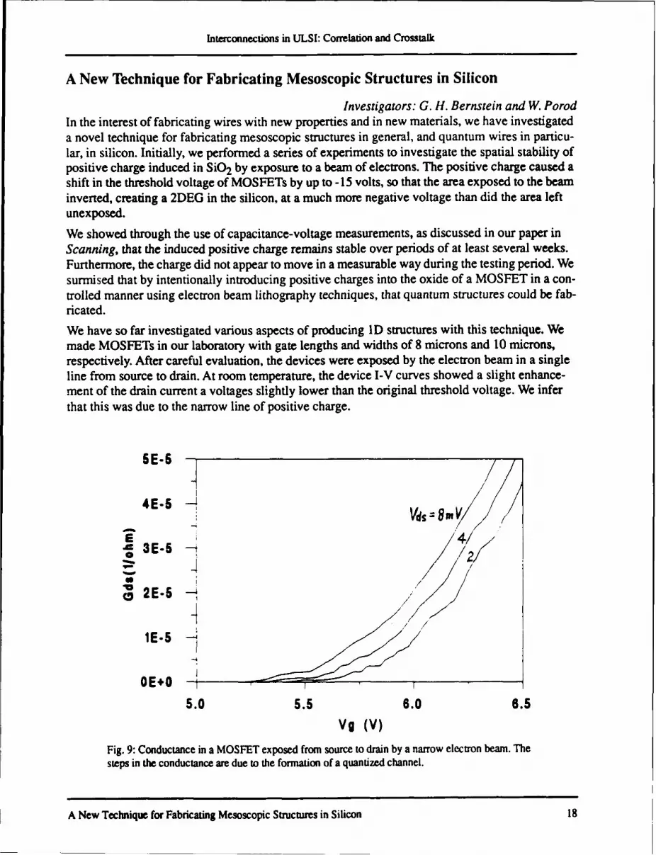
We have so far investigated various aspects of producing ID structures with this technique. Wemade MOSFETs in our laboratory with gate lengths and widths of 8 microns and 10 microns,respectively. After careful evaluation, the devices were exposed by the electron beam in a singleline from source to drain. At room temperature, the device I-V curves showed a slight enhance-ment of the drain current a voltages slightly lower than the original threshold voltage. We inferthat this was due to the narrow line of positive charge.
5E-5 6
4E-5Vds=
i 413E 65a //
0 2E-5 -
"1E-5 -
OE+O - I
5.0 5.5 6.0 6.5
Vg (V)
Fig. 9: Conductance in a MOSFET exposed from source to drain by a narrow electron beam. The
steps in the conductance are due to the formation of a quantized channel.
A New Technique for Fabricating Mesoscopic Structures in Silicon 18
Interconnections in ULSI: Correlation and Crosstalk
We tested several devices, both exposed and unexposed at 1.8K. Among the unexposed devices,the Notre Dame devices and commercially fabricated devices showed no structure whatsoeveraround the threshold voltages. All of the exposed devices showed complicated structure veryclose to threshold. One set of conductance data as a function of the gate voltage for differentdrain/source voltages is shown in Fig. 9. The steps indicate that right at threshold, the line doesnot invert uniformly, leaving a pinched area or areas in series with the resistance of the channel.Steps are clearly evident, although they do not appear in units of e2/4h, as they ought to for pointcontacts in silicon. We concluded that the lack of predictable step size in the conductance was dueto the large series resistance of the ID channel. We are in the process of performing more experi-ments on this system and are preparing a manuscript regarding the preliminary results.
Relevant Publications:
G. H. Bernstein, S. W. Polchlopek, R. Kamath, and W. Porod, "Determination of Fixed Electron-Beam-Induced Positive Oxide Charge," Scanning 14, 345 - 349 (1992).
A New Technique for Fabricating Mesoscopic Strctures in Silicon 19

Inter.onnections in ULSI: Correlation and Crosstak
Journal Publications
*Items marked with an asterisk are included in the appendix.
*S. Bandyopadhyay, "Coupling and Crosstalk Between High Speed Interconnects in Ultra LargeScale Integrated Circuits," IEEE Journal of Quantum Electronics 28, 1554 - 1561 (1992).
* G. H. Bernstein, D. A. Hill and W. P. Liu, "New High-Contrast Developers for PMMA Resist,"Journal of Applied Physics 71, 4066 - 4075 (1992).
* S. J. Koester, G. Bazan, G. H. Bernstein, and W. Porod, "Fabrication of Ultrasmall Tunnel Junc-tions by Electron Beam Lithography," Review of Scientific Instruments 63, 1918 - 1921 (1992).
S. Subramaniam, S. Bandyopadhyay, B. Das, G. H. Bernstein, and P. A. Sekula-Moise, "Anoma-lous Magnetoresistance Due to Correlations Between Disorder and Boundary Scaterings in aTwo-Dimensional Electron Gas Channel," Physical Review B 45, 3826 - 3829 (1992).
N. Telang and S. Bandyopadhyay, "A Monte Carlo Study of Correlations Between Impurity Scat-tering Events in a Two dimensional Electron Gas Causing Inhomogeneous Magnetoresistance,"Superlattices and Microstructures 11, 99 - 102 (1992).
* Henry K. Harbury, Wolfgang Porod, and Craig S. Lent, "Field Effects in Self-Consistent Trans-port Calculations for Narrow Split-Gate Structures," Superlattices and Microstructures 11, 189- 193 (1992).
* G. H. Bernstein and D. A. Hill, "On the Attainment of Optimum Development Parameters forPMMA Resist," Superlattices and Microstructures 11, 237-240 (1992).
S. Chaudhuri and S. Bandyopadhyay, "Quantum Transport in a Disordered Quantum Wire in thePresence of a Magnetic Field," Superlattices and Microstructures 11, 241 - 244 (1992).
S. Chaudhuri and S. Bandyopadhyay, "Spatial Distribution of the Current and Fermi CarriersAround Localized Elastic Scatterers in Quantum Transport," Physical Review B 45, 11126 -11135 (1992).
* S. Chaudhuri and S. Bandyopadhyay, "Numerical Calculation of Hybrid Magnetoelectric States
in an Electron Waveguide, Journal of Applied Physics 71, 3027 - 3029 (1992).
Henry K. Harbury, Wolfgang Porod, and Stephen M. Goodnick, "Lateral p-n junctions betweenquasi two-dimensional electron and hole systems at corrugated GaAs/A1GaAs interfaces,"Journal of Vacuum Science and Technology B 10, 2051 - 2055 (1992).
* Wolfgang Porod, Zhi-an Shao, and Craig S. Lent, "Transmission Resonances and Zeros in Quan-tum Waveguides with Resonantly-Coupled Cavities," Applied Physics Letters 61, 1350 - 1352(1992).
* Wolfgang Porod, Henry K. Harbury, and Stephen M. Goodnick, "Lateral p-n junctions and quan-tum wires formed by quasi two-dimensional electron and hole systems at corrugated GaAs/AlGaAs interfaces," Applied Physics Letters 61, 1823 - 1825 (1992).
* X. Huang, G. Bazan, G. H. Bernstein, and D. A. Hill, "Stability of Thin Resist Walls," Journal ofthe Electrochemical Society 139, 2952-2956 (1992).
* G. H. Bernstein, S. W. Polchlopek, R. Kamath, and W. Porod, "Determination of Fixed Electron-Beam-Induced Positive Oxide Charge," Scanning 14, 345 - 349 (1992).
Journal Publicati 20

Interconnections in ULSI: Correlation and Crosstalk
* D. A. Hill, X. Huang, G. Bazan, and G. H. Bemstein, "Swelling and Surface Forces-InducedInstabilities in Nanoscopic Polymeric Structures," Journal of Applied Physics 72, 4088-4094(1992).
* S. Bandyopadhyay, S. Chaudhuri, B. Das, and M. Cahay, "Features of quantum magnetotransportand electromigration in mesoscopic systems," Superlattices and Microstructures 12, 123 - 132(1992).
L. Rota, F. Rossi, S. M. Goodnick, P. Lugli, E. Molinari, and W. Porod, "Reduced carrier coolingand thermalization in semiconductor quantum wires," Physical Review B 47, 1632 - 1635(1993).
N. Telang and S. Bandyopadhyay, "The effect of collision retardation on hot electron transport ina quantum well," Physical Review B 47, 9900 (1993).
S. W. Polchlopek, G. H. Bernstein, and R. Kwor, "Properties of Nitrogen Implanted SOI Sub-strates," IEEE Transactions on Electron Devices 40, 385 - 391 (1993).
* S. Chaudhuri, S. Bandyopadhyay, and M. Cahay, "Spatial distribution of the current, Fermi carrierdensity, potential and electric field in a disordered quantum wire in a magnetic field," PhysicalReview B 47, 12649 (1993).
* Craig S. Lent, P. Douglas Tougaw, and Wolfgang Porod, "Bistable saturation in coupled quantum
dots for quantum cellular automata," Applied Physics Letters 62, 714 - 716 (1993).
* Craig S. Lent, P. Douglas Tougaw, Wolfgang Porod, and Gary H. Bernstein, "Quantum CellularAutomata," Nanotechnology 4, 59 - 57 (1993).
N. Telang and S. Bandyopadhyay, "Quenching of Acoustic Phonon Scattering of Electrons inSemiconductor Quantum Wires Induced by a Magnetic Field," Applied Physics Letters 62,3161 (1993).
* Henry K. Harbury, Wolfgang Porod, and Stephen M. Goodnick, "A Novel Quantum Wire Formedby Lateral p-n-p Junctions Between Quasi-Two-Dimensional Electron and Hole Systems atCorrugated GaAs/AlGaAs Interfaces," Journal of Applied Physics 73, 1509 - 1520 (1993).
* P. Douglas Tougaw, Craig S. Lent, and Wolfgang Porod, "Bistable Saturation in Coupled Quan-tum-Dot Cells," Journal of Applied Physics 74, 3558 - 3566 (1993).
* Wolfgang Porod, Zhi-an Shao, and Craig S. Lent, "Resonance-Antiresonance Line Shape forTransmission in Quantum Waveguides with Resonantly-Coupled Cavities," Physical Review B48,8495 - 8498 (1993).
* X. Huang, G. H. Bernstein, G. Bazan, and D. A. Hill, "Spatial Density of Lines in PMMA byElectron Beam Lithography," Journal of Vacuum Science and Technology A 11, 1739-1744(1993).
* G. Bazan and G. H. Bernstein, "Electron Beam Lithography Over Very Large Scan Fields," Jour-nal of Vacuum Science and Technology A 11, 1745-1752 (1993).
* X. Huang, G. Bazan, G. H. Bernstein, "New Technique for Computation and Challenges for Elec-tron Beam Lithography," Journal of Vacuum Science and Technology B 11, 2665 - 2569 (1993).
N. Telang and S. Bandyopadhyay, "The Effect of a Magnetic Field on Polar Optical and SurfacePhonon Scattering Rates," Physical Review B 48 (Dec 15 - 1993).
Journal Publications 21

Interconnections in ULSI: Correlation and Crosstalk
Minhan Chen, Wolfgang Porod, and David J. Kirkner, "A Coupled Finite Element/Boundary Ele-ment Method for Semiconductor Quantum Devices with Exposed Surfaces," Journal of AppliedPhysics 75 (Mar I - 1994).
M. Cahay and S. Bandyopadhyay, "Quantum Devices" Advances in Electron Physics (Invited, inpress).
N. Telang and S. Bandyopadhyay, "'Modulation of Electron Phonon Scattering in Quantum Wiresby a Magnetic Field," Semiconductor Science and Technology (in press).
Zhi-an Shao, Wolfgang Porod, and Craig S. Lent, "Transmission Resonances and Zeros in Quan-tum Waveguide Systems with Attached Resonators," Physical Review B (in press).
G. H. Bernstein, R. J. Minniti, Jr., and X. Huang, "An Advanced IC Processing Laboratory at theUniversity of Notre Dame," IEEE Transactions on Education (in press).
Journm Pubflicaions 22
Interconnections in ULSI: Correlation and Crosstalk
Conference Publications and Presentations
N. M. Jisrawi, S. J. Koester, Q. Lu, M. J. Honkanen, W. Porod, G. H. Bernstein, and S. T. Ruggi-ero, "Microwave Studies of Single Electron Charging Effects," abstract published in the Bulle-tin of the APS, Vol. 36, No. 3, p. 872, March 1991; presented at the 1991 March Meeting of theAmerican Physical Society, Cincinnati, Ohio, March 1991.
H. K. Harbury, W. Porod, and C. S. Lent, "Self-Consistent Calculation of Coherent Transport inSplit-Gate Structures, abstract published in the Bulletin of the APS, Vol. 36, No. 3, p. 1049,March 1991; presented at the 1991 March Meeting of the American Physical Society, Cincin-nati, Ohio, March 1991.
W. Porod, (Invited), "A Monte Carlo Model of High - Field Electronic Transport and Hot ElectronTrapping/Detrapping in SiO2 ," Proceedings of the Seventh International Conference on theNumerical Analysis of Semiconductor Devices and Integrated Circuits, NASECODE-7, Ed. byJJH Miller, pp. 81 - 82; presented at the Seventh International Conference on the NumericalAnalysis of Semiconductor Devices and Integrated Circuits, NASECODE-7, Copper Mountain,Colorado, April 1991.
H. K. Harbury, W. Porod, and C. S. Lent, "Self-Consistent Calculation of Coherent Transport inSplit-Gate Structures," Proceedings of the Seventh International Conference on the NumericalAnalysis of Semiconductor Devices and Integrated Circuits, NASECODE-7, Ed. by JJH Miller,pp. 136 - 137; presented at the Seventh International Conference on the Numerical Analysis ofSemiconductor Devices and Integrated Circuits, NASECODE-7, Copper Mountain, Colorado,April 1991.
Wolfgang Porod, (Invited), "Computation in Granular Flatland: Discrete Space -- Time CellularAutomata," presented at the Granular Nanoelectronics Workshop, Urbana, Illinois, May 1991.
Henry K. Harbury, Wolfgang Porod, and Craig S. Lent, "Local-Field Effects in Self-ConsistentTransport Calculations for Narrow Split-Gate Structures," presented at the International Sym-posium on Nanostructures and Mesoscopic Systems, Santa Fe, New Mexico, May 1991.
G. H. Bernstein and D. A. Hill, "On the Attainment of Optimum Development Parameters forPMMA Resist," poster presented at the International Symposium on Nanostructures and Meso-scopic Systems, Santa Fe, New Mexico, May 1991.
Wolfgang Porod, (Invited), "Locally - Interconnected Architectures," presented at the DSRCIDARPA Workshop on Cellular Automata and Quantum Devices, La Jolla, California, July 1991.
Henry Harbury, Wolfgang Porod, and Stephen M. Goodnick, "Lateral p-n junctions between quasitwo-dimensional electron and hole systems at corrugated GaAs/A1GaAs interfaces," presentedat the 19th International Conference on the Physics and Chemistry of Semiconductor Inter-faces, PCSI-19, Death Valley, January 1992.
Paul D. Tougaw, Craig S. Lent, Wolfgang Porod and G. H. Bernstein, "Cellular automata rulesderived from quantum dot coupling," abstract published in the Bulletin of the APS, Vol. 37, No.1, p. 135, March 1992; presented at the 1992 March Meeting of the American Physical Society,Indianapolis, Indiana, March 1992.
Henry K. Harbury, Wolfgang Porod, and Stephen M. Goodnick, "Lateral p-n junctions betweenquasi two dimensional electron and hole systems at corrugated GaAs/AlGaAs interfaces,"
Conference Publications and PresenLations 23

Interconnections in ULSI: Correlation and Crosstalk
abstract published in the Bulletin of the APS, Vol. 37, No. 1, p. 324, March 1992; presented atthe 1992 March Meeting of the American Physical Society, Indianapolis, Indiana, March 1992.
Wolfgang Porod, Henry K. Harbury, and Gary H. Bernstein, "A Study of Cellular AutomataArchitectures for Integrated Quantum Device Arrays Using the Helmholtz Equations as a Com-putational Model," abstract published in the Bulletin of the APS, Vol. 37, No. 1, pp. 134 -- 135,March 1992; presented at the 1992 March Meeting of the American Physical Society, Indianap-olis, Indiana, March 1992.
Zhi-an Shao, Wolfgang Porod, and Craig S. Lent, "Transmission Resonances and Zeros in Quan-tum Waveguide Structures," abstract published in the Bulletin of the APS, Vol. 37, No. 1, pp.289 -- 290, March 1992; presented at the 1992 March Meeting of the American Physical Soci-ety, Indianapolis, Indiana, March 1992.
Lucio Rota, Stephen M. Goodnick, Wolfgang Porod, Fausto Rossi, and Paolo Lugli, "Electron-Electron Interaction in Multisubband Quantum Wires," abstract published in the Bulletin of theAPS, Vol. 37, No. 1, p. 239, March 1992; presented at the 1992 March Meeting of the AmericanPhysical Society, Indianapolis, Indiana, March 1992.
S. Chaudhuri, S. Bandyopadhyay and M. Cahay, "Spatial distribution of current and the Fermidensity of states around impurities in phase coherent transport," presented at the 1992 MarchMeeting of the American Physical Society, Indianapolis, Indiana, March 1992.
S. Bandyopadhyay, S. Chaudhuri and M. Cahay, "Two dimensional current and probability den-sity profiles in mesoscopic systems in the presence of a magnetic field," presented at the 1992March Meeting of the American Physical Society, Indianapolis, Indiana, March 1992.
S. Chaudhuri, S. Bandyopadhyay and M. Cahay, "Study of universal conductance fluctuations andquenching of Anderson localization in a megntic field: a Weber function analysis," presented atthe 1992 March Meeting of the American Physical Society, Indianapolis, Indiana, March 1992.
S. Bandyopadhyay, "Electromagnetic and quantum mechanical coupling between narrow inter-connects in ULSI," presented at the 1992 March Meeting of the American Physical Society,Indianapolis, Indiana, March 1992.
N. Telang and S. Bandyopadhyay, "A Monte Carlo study of correlations between impurity scatter-ing events giving rise to anomalous magnetoresistance in a 2 DEG," presented at the 1992March Meeting of the American Physical Society, Indianapolis, Indiana, March 1992.
N. Telang and S. Bandyopadhyay, "The effect of finite colision duration on hot electron transportin a quantum well," presented at the 1992 March Meeting of the American Physical Society,Indianapolis, Indiana, March 1992.
S. Subramaniam, S. Bandyopadhyay, B. Das, and G. H. Bernstein, "Anomalous magnetoresis-tance due to correlations between scattering events in an InGaAs/AlGaAs quantum well," pre-sented at the 1992 March Meeting of the American Physical Society, Indianapolis, Indiana,March 1992.
X. Huang, S. Subramaniam, G. H. Bernstein, and S. Bandyopadhyay, "Nanolithographic Fabrica-tion of Narrow Metal Lines," presented at the 1992 March Meeting of the American PhysicalSociety, Indianapolis, Indiana, March 1992.
G. H. Bernstein and X. Huang, "Fabrication of Interconnect Structures for Quantum Based Archi-
Conference Publications and Presentations 24

Interconnections in ULSI: Correlation and Crosstalk
tectures," presented at the 1992 March Meeting of the American Physical Society, Indianapolis,Indiana, March 1992.
B. Das, S. Subramaniam, S. Bandyopadhyay, and G. H. Bernstein, "Electron beam damage duringelectron beam lithography in modulation doped heterostructures," presented at the 1992 MarchMeeting of the American Physical Society, Indianapolis, Indiana, March 1992.
L. Rota, F. Rossi, P. Lugli, E. Molinari, S. M. Goodnick, and W. Porod, "Monte Carlo Simulationof a True' Quantum Wire," presented at the 1992 Symposium on Compound SemiconductorPhysics and Devices, of SPIE - The International Society of Optical Engineering, Somerset,New Jersey, March 1992.
M. Cahay, T. Singh and S. Bandyopadhyay, "Electron emission from a quantum well as a result ofexchange and Coulomb interactions," Proceedings of the International Workshop on Computa-tional Electronics, pp. 147 - 150; presented at the International Workshop on ComputationalElectronics, Urbana, Illinois, May 1992.
Craig S. Lent, Douglas Tougaw, and Wolfgang Porod, "A Bistable Quantum Cell for CellularAutomata," Proceedings of the International Workshop on Computational Electronics, pp. 163- 166; presented at the International Workshop on Computational Electronics, Urbana, Illinois,May 1992.
N. Telang and S. Bandyopadhyay, "Electron phonon scattering in quantum wires subjected tohigh magnetic field," Proceedings of the International Workshop on Computational Electron-ics, 237 - 240; presented at the International Workshop on Computational Electronics, Urbana,Illinois, May 1992.
Henry K. Harbury, Wolfgang Porod, and Stephen M. Goodnick, "A Numerical Study of Lateral p-n Junctions between Quasi TIwo-Dimensional Electron and Hole Systems at Corrugated GaAs/AlGaAs Interfaces," Proceedings of the International Workshop on Computational Electronics,pp. 249 - 251; presented at the International Workshop on Computational Electronics, Urbana,Illinois, May 1992.
Zhi-an Shao, Wolfgang Porod, and Craig S. Lent, "A Numerical Study of Transmission Reso-nances and Zeros in Quantum Waveguide Structures," Proceedings of the International Work-shop on Computational Electronics, pp. 253 - 256; presented at the International Workshop onComputational Electronics, Urbana, Illinois, May 1992.
S. Chaudhuri, S. Bandyopadhyay and M. Cahay, "Numerical study of quantum magnetotransportin disorderd non-adiabatic constrictions," Proceedings of the International Workshop on Com-putational Electronics, 305 - 308; presented at the International Workshop on ComputationalElectronics, Urbana, Illinois, May 1992.
S. Bandyopadhyay, S. Chaudhuri, B. Das, and M. Cahay, (Invited), "Magnetotranpsort and elec-tromigration in mesoscopic systems," Sixth International Conference on Superlattices andMicrostructures, Xian, People's Republic of China, August 1992.
R. E. Bartolo, N. Giordano, X. Huang, and G. H. Bernstein, "Giant Oscillations in MesoscopicPhotovoltaic Effect," poster presented at the 40th Midwest Solid State Conference (Judged Sec-ond-Best Poster at Conference.), Urbana, Illlinois, October 1992.
G. H. Bernstein, D. A. Hill, X. Huang, and G. Bazan, "Failure Mechanisms of Very Narrow
Conference Publications and Presentations 25

Interconnections in ULSI: Correlation and Crosstalk
PMMA Walls," presented at the 39th National Symposium of the American Vacuum Society,Chicago, Illinois, November 1992.
G. Bazan and G. H. Bernstein, "Electron Beam Lithography Over Large Scan Fields," presentedat the 39th National Symposium of the American Vacuum Society, Chicago, Illinois, November1992.
R. Frankovic and G. H. Bernstein, "Observation of Current-Induced Failures of Ultra-NarrowMetal Interconnects," poster presented at the 39th National Symposium of the American Vac-uum Society, Chicago, Illinois, November 1992.
Craig S. Lent, P. Douglas Tougaw, Wolfgang Porod, and Gary Bernstein, "Quantum CellularAutomata," presented at the International Symposium on New Phenomena in MesoscopicStructures, Maui, Hawaii, December 1992.
Henry K. Harbury, Wolfgang Porod, and Stephen M. Goodnick, "Novel Quantum Wire Formedby Lateral p-n-p Junctions Between Quasi-Two-Dimensional Electron and Hole Systems atCorrugated GaAs/AlGaAs Interfaces," presented at the International Workshop on QuantumStructures, Santa Barbara, California, March 1993.
Craig S. Lent, P. Douglas Tougaw, Wolfgang Porod, and Gary Bernstein, "Quantum CellularAutomata," presented at the International Workshop on Quantum Structures, Santa Barbara,California, March 1993.
S. Bandyopadhyay, B. Das, M. Cahay and S. Chaudhuri, "Low Temperature Conduction in Ultra-narrow Wires: Quantum Transport and Weak Electromigration Causing 1/f Noise," presented atthe 183rd Meeting of the Electrochemical Society, Honolulu, Hawaii, May 1993.
N. Telang and S. Bandyopadhyay, "Influence of Phonons on Electromigration in UltranarrowWires," presented at the 183rd Meeting of the Electrochemical Society, Honolulu, Hawaii, May1993.
Gary H. Bernstein, Xiaokan Huang, Greg Bazan, Davide A. Hill, Craig S. Lent, and WolfgangPorod, "New Technique for Computation and Challenges for Electron Beam Lithography," pre-sented at the Three-Beam Conference, San Diego, California, June 1993.
Henry K. Harbury and Wolfgang Porod, "Numerical Linear Response Study of the Electron WindForce of Electromigration in Quasi-ID Transport," presented at the International Workshop onComputational Electronics, Leeds, England, August 1993.
Minhan Chen, Wolfgang Porod, and David J. Kirkner, "Boundary Conditions for QuantumDevices with Exposed Surfaces," presented at the International Workshop on ComputationalElectronics, Leeds, England, August 1993.
Zhi-an Shao, Wolfgang Porod, and Craig S. Lent, "Resonance/Antiresonance Lineshape forTransmission in Quantum Waveguides with Resonantly-Coupled Cavities," presented at theInternational Workshop on Computational Electronics, Leeds, England, August 1993.
Craig S. Lent, Wolfgang Porod, and P. Douglas Tougaw, "Quantum Simulation of Several-ParticleSystems," presented at the International Workshop on Computational Electronics, Leeds,England, August 1993.
N. Telang and S. Bandyopadhyay, "Modulation of Electron-Phonon Scattering Rates in Quantum
Conference Publications and Presentations 26

Interconnections in ULSI: Correlation and Crosstalk
Wires by a Magnetic Field," presented at the International Conference on Hot Carriers in Semi-conductors, Oxford, England, August 1993.
Craig S. Lent, P. Douglas Tougaw, Wolfgang Porod, and Gary H. Bernstein, (Invited), "QuantumCellular Automata," presented at the 21st Midwest Solid State Theory Symposium, Detroit,Michigan, October 1993.
Craig S. Lent, P. Douglas Tougaw, Wolfgang Porod, and Gary H. Bernstein, (Invited), "QuantumCellular Automata," presented at the ARPA ULTRA Program Review, Santa Fe, New Mexico,October 1993.
Conference Publications and Presentations 27

1554 IEEE JOURNAL OF QUANt'M ELECTRONICS. VOL 28. NO 6. JUNE 19Q2
Coupling and Crosstalk Between High SpeedInterconnects in Ultralarge Scale
Integrated CircuitsSupnyo Bandvopadhyay, Senior Member. IEEE
AbstvWc--Tbe advent of sophisticated lithographic tech- grown by wet oxidation). In addition to causing crosstalk,niques has made it possible to fabricate densely packed ultra- tunneling can give rise to a unique problem. In multilay-large-scale-integrated (ULSI) circuits. In these chips. Intercon-nectt o ro d sp t ered interconnects, there can be crossings of two lines withsignal from one line could easily get coupled to another causing a very thin dielectric layer sandwiched between them. Ifinterference and crosstalk. This paper presents a general the- the thickness of the lines is a few hundred angstroms, thenory to model coupling between optical interconnects (wave- at the crossing we have a crossover capacitor whose ef-guides) and quantum-mechanical coupling between narrow and fective plate area is a few hundred angstroms square andvery closely spaced silicide interconnects embedded in dielec- the plate separation is also of the same order. The conre-trics (SiOl). sponding capacitance can be estimated from standard for-
mula [81. If the iinewidths are 300 A and teo plus sep-aration is 100 A, then the crossover capacitance is
I. INTRODUCTION 1- 10-7 F. Since the dielectric layer betiwem te plates isR ECENT advances in nanolithography [11]-[61 have thin enough, an electron can tunnel through this layer from
made it possible to delineate electronic devices with one interconnect to another. Such tunneling can charge upfeature sizes of a few hundred angstroms in both silicon the capacitor to 10 mV per electron! Effects such as theseand GaAs wafers. The ability to make such small features have already been observed in single discrete capacitorshas led to the development of ultralarge-scale-integrated [9]. Obviously, stray voltages of this nature are undesir-(ULSI) circuits with packing densities far greater than able in an integrated circuit and can cause reliability prob-those of very-large-scale-integrated (VLSI) circuits. In lems, logic errors, etc., especially if the supply voltages1980, Hewlett-Packard produced a single chip micropro- have been scaled down with the device sizes.cessor with 0.5 million devices on a 1 sq um chip using The close physical proximity of neighboring lines is not1.25 •m feature sizes [7]. Today, we are envisioning chips the only cause of increased coupling in ULSI. The in-with 109 devices. Simple scaling law shows that the fea- creasing length of interconnects with increasing chip sizeture sizes required for such ULSI chips will be a few also contributes to increased coupling since a larger re-hundred angstroms causing extremely dense packing. gion is available for interaction when the interconnects
In ULSI chips not only are the devices densely packed, are long. Suffice it to say, then, that crosstak and cou-but so are the interconnects. The close proximity of in- pling can be a serious problem in large ULSI chips be-terconnect lines resulting from this dense packing could cause of the dense packing and long interconnect length.lead to severe problems with mutual interference and To understand the nature of this coupling and finally tocrosstalk. In this paper, we study crosstalk due to cou- find ways of countering it, one needs to be able to de-pling between optical interconnects (GaAs waveguides scribe and model such coupling effects within a basic mi-embedded in AIGaAs) and coupling between narrow and croscopic formalism. In this paper, we present such aclosely spaced silicide interconnects surrounded by a di- model derived from general coupled mode theory [101-electric. In the case of silicide interconnects, coupling is [18). The formalism is perfectly general and applies forcaused by quantum-mechanical tunneling of electrons coupling between both optical and silicide interconnects.from one line to another. This kind of coupling will be i.e., for both optical coupling and quantum mechanicalespecially severe if the dielectric in which the intercon- coupling (tunneling). The applicability of the model fornects are embedded is leaky (such as porous Si 3N4 or SiO 2 both types of coupling is a rather fortuitous coincidence
which happens because the basic equations describing theManuscnpt received August 23. 1991; revised December 4. 1991. This two types of coupling at the microscopic level are the
work was supported by the Office of Naval Research by Grant N00014-91- electromagnetic wave equation (derived from Maxwell'sI-1505 and by IBM through a Faculty Development Award. equation) and the Schrodinger equation which are math-
The author is with the Department of Elecmncal Engineenng. Universityof Notre Dame. Notre Dame. IN 46556. ematically similar. In the next section. we present the the-
IEEE Log Number 9107782. ory and then the Section III we estimate coupling coeffi-
0018-9197/92503.00 © 1992 IEEE

BANDYOPADHYAY COUPLING AND CROSSTALK IN ULSI INTERCONNECTS 1555
cients for both types of coupling. In Section IV we present Using (3). we can replace the terms within the squareresults for GaAs-AIGaAs optical interconnects and sili- brackets in the left-hand side of (4) to getcide interconnects. Finally. in Section V. we present the 2Lconclusions. -_-. -
ax,II. THEORY + A"- a- )
A. Coupling Between Optical Interconnects -
To model electromagnetic coupling between a set of (5)closely spaced optical interconnect lines, we view and theinterconnects as optical waveguides and start from the Finally, multiplying the above equation by & (thewave equation that governs the propagation of an electro- asterisk denotes complex conjugate) and integrating overmagnetic signal in a waveguide. We assume that the in- all space, we obtain the coupled set of equations for theterconnects are nonlossy and nondispersive. This is a veryv coefficients C,
good assumption for optical interconnects comprising (a"Co 2 COGaAs waveguides surrounded by AIGaAs cladding. Thex0 +ita C( - - . 0
scalar wave equation for a TE mode propagating in the I
.i direction in any one waveguide reads [101 (m = 1. 2. 3. .n) (6)a2 Ev a" where .., j d3 ro *(a 2 /at 2)[P,]ya and O, is
V 2 E,,(Ft) =/e + • [P~ (F, t)]y, (1) the overlap between the fields in the mth and nth inter-
connect (O, = j d 3 r& C ).where E, is the y component of the electric field in the Equation (6) is a set of n coupled second order differ-
interconnect (waveguide) and [Pco] is the y component ential equations. The difference between (6) and the equa-of a distributed polarization source caused by the coupling tions of conventional coupled mode theory is that we haveof signal from other interconnects. The quantities A and c not assumed Om. = 0 for m * n. In fact, this assumptionare the permeability and permittivity of the interconnects, would be incorrect in the limit of strong coupling where
To solve for the field E in the above equation, we in- the overlap between the fields in neighboring intercon-yoke standard coupled mode theory. The solution nects can be quite significant and neglecting this overlapE,( F, t) can be written as a linear superposition of the may result in violation of energy conservation [131-1181.normal modes (unperturbed fields) in the individual inter- Let us now make the following substitutionconnects
E t) = 0 C(x)&4 (y, z)e"' (2) ),,(x) = C.(x) exp -i k,, dx (7)
where &( y, z) is the y component of the electric field in wherethe isolated nth interconnect (in the absence of coupling) (k.)2 = /I (W Woo). (8)and w' is the signal frequency. The field Q2(y, z) satisfies(the unperturbed wave equation so that Substituting (7) in (6) and using (8), we get
rA:~ [aDI,.aDI011")(y, z)e"`' ax- -T20., + 2ik ^0.- - K1O1M-
o v2 2 anv)a
f a2-vni(Y.e = -w'isdt&'(y, O)ef"' •exp i kdx =O (m = 1,2.3,'" ,n).
(3) (9)
where wo is the signal frequency in the nth interconnect. Equation (9) can be recast in a matrix form
Substituting (2) in (I). we get a2 ba
a2 c. + C a2 [Al + [ + 2i[B l [I e [KW [iX] (10)
C + ,., z)e" where [151 is ann X I matrix whose elements are the coef-ficients 61, L5, ' D.,, [A) is an n x n matrix whose
-- -2a C,8, l(y. zl W*-Aew. C.~ .Z)l e~w elements are Amp,= 0,, exp (i f k., dx). [B] is an 4 n
_ matrix whose elements are B,. = k.,O,,, exp (i I k, dx)2 and [K] is an n x n matrix whose elements are given by
a C.8.(y, Z) e (4) K,.. = K, exp (i I k, dx).Equation 10 is the general coupled mode equations for
where [P,( F. t)], is an operator such that [P o l,( F, t), a system of n optical interconnects. To illustrate the use-8, = 0 1)' . fulness of these equations. we now proceed to solve them
Sit, :FEEl JOURNAL oF ,)LAsrum ELECTRONICS. VOL_ 28. NO 6. JUNE 1992
for the case of just two interconnects. For this. we first The above equations can be decoupled to yieldnote that ratio of the second to the first term in the LHSof (10) is of the order of the ratio ot the distance scale -D - ilk; - '__ -3D - 012,1D = 0 (15)over which significant coupling occurs to the wavelength .r - xof the signal in the interconnects. For electromagnetic whose solution iscoupling, the signal wavelength is the wavelength of theoptical or electromagnetic signal which is between I and D1 (x = e'afPe'•' Qe-"i] (16)100 gsm typically. (We are only concerned with high speed where P and Q are constants. 26 = k' - k, and v=interconnects. i.e.. optical interconnects or those that vK2 + 2 where K = Q f2I1 The last equality followscarry ultrashort pulses or millimeter waves.) For quantum from the fact that the two interconnects are assumed to bemechanical coupling the wavelength is the DeBroglie identical.wavelength of electrons which is between 10 and 100 A.Since even for the most densely packed interconnects, we sumin ta te wav vectors a nd ofp)do not expect significant coupling to occur over such smallscales, we can always neglect the first term in the LHS of Ci(x) = e'k°'[Pe'x + Qe-D'] (17)(GO) in comparison with the second term. This allows us where k0 = k, + k.to obtain closed analytical solutions of (10) in the case of Similarly, we gettwo interconnects.
If we neglect the first term in the LHS (10), we get Cx) = -e'Lz[Pp'e'Yx + Q'e-VIX] (18)
a = A - i11 12D exp -i [k, - k, where P' = Pk+/K and Q' = Qk/i with k, + 25 +
2x 2andk =26- 2v.a-- -k - To evaluate the constants P and Q, we need to applya =- iA,2D2 - i, 2 /I D exp -i [k2 - kdx the boundary conditions. Let
(11) Ci(x =0) =P + Q =A+where k P + k (19)
1 KiIO0,, K2 012 1KAi = - Lk( t1022 --iO21) k,(0 110 22 - 1012 This gives
I K' OilK 2 02 ,,,_ot 1 k KA, 22 1~2 0 ) P =--A+ - A2 Lk(0 1102 2 - 101212) k,(0 11022 - 1012) 2- 1 2P22
1011 1(O'21 K2Q = - A + -A (20)=- LkO,,0 22 - IO,2 -- k,(,OtO,-k IO,1.I-, -, + -
I F _____0___ '.2012 1 Now let
2 [ko01o 22 - 10121) k,(0,10 2 - 10,2 1 )]. Cx = L)= B+
(12) C2(x =L)= B (2-L)
We now make another transformation of variables Using (16)-(20). we get
D, =Dtexp 1-i Bd+x B e'kL [(cos (PL) + -sin(,L), At
D52 = D, exp -i _, dx + (•- sin (vL) A•
= k; + A, ik jsB = e'l cos KL) -- sin K) A+
k, = k" + A,. (13) v
This reduces (11) to + -- sin (VL) A . (22)
" "11_fl2D, exp -i [k, - k,.dxa- = This equation can be written in a matrix form as
3D -if 1 1 Dexp i fk.-k]dx}. (14) (B) = (a c) . (,) 23)ax = QD \x a[,- ild ,' b d \A2/(
3.NDYOPADHYAY COUPLING AND (RoSST-LK 1 ,, l i\TFRCONFCTS 1557
where function. Ho is the unperturbed Hamiltonian. and H' isthe perturbation in the Hamiltonian arising from coupling.
a e`'"L cos (PL -,- -smin PvL We will assume that the perturbation is static (this ne-"..',,lects phonon-assisted or incoherent tunneling) and use
time-independent perturbation theory. The wave functionh c = e ( sin (PiL) is written as
,1) cr. v Z. t) = C,(X) Y, Z)d =eKL (ecos (vL)- - sin (vL) (24) , C=(x)y,(y. z)Je=I)Ely (30)
Note that the 2 x 2 matrix in (23) is in the form of a where O1.2( Y, z)e -,E,'t/h are the unperturbed wave func-transmission matrix. The matrix element b (= c) is an tions in interconnects I and 2 in the absence of coupling.indication of the coupling from one interconnect to an- These wave functions are eigen functions of Ho (which isother. It is the fraction of the signal in interconnect I that Hermitean) and therefore orthonormal.gets coupled to interconnect 2 after a distance L. Substi- Since 01.2 ( Y, z)e -,E, :,/h are eigen functions of H0 , i.e.,tuting back the values of K and v. we find that the quantity they satisfy the unperturbed Schridinger equation, it isb is given by easy to see that
bi = ci K sin 6S2LI. (25) H0o ,1.(y, z) = E1.. •.2( Y, z). (31)
Substituting (30) in (29). we getIt is easy to show that this coupling is maximum if 6 = 0 h 2 (a2 C1 a a2 a2 21as long as tan (.L) > KL or as long as KL s r/2. To -2m ý-+C, + [ a 2
have 6 = 0 would require that the two interconnects beidentical and carry the same signal frequency. Note that _
2 c 2 [a aC212
when 6 is zero it is possible for 100% of the signal in one - 2m (X2ax + C a Va2 az2
interconnect to get coupled to the other and this happens . + C, 0 H'(CO, + C2 02) (32)at a distance
= where 01,2 - 01.2(Y. z)e-kr.
L0o% =(26) Comparing the above equation with (5), we find thatthey are mathematically similar. This is not surprising
In the case of 6 = 0, the coupling over a distance L is since both the electromagnetic wave equaion and thesimply given by Schr6dinger equation describe the propagation of a wave
through a medium. Because of this mathematical similar-Ibl = I! = tsin (.)I (27) ity we can write down the coupling coefficients hbi and
Therefore. the fraction of the signal power from one in- Ici from analogy without any further derivation.terconnection that is coupled into another is given by Ib# = 1c = sin (CL) (33)
bJ2 = IC12 = isin (KL.)l:. (28) where
The most important step now is to derive an expression (mHi /h 2 )011 - (mfH;. I /h 2)021
for the coupling constant K. But before we proceed to do "so. we show that the Schrddinger equation governing 0(O1O22 _ 10-21")quantum mechanical coupling between interconnect lines (m H .. I/h)0 2 . - (mIHi,, I/ h2)012) (34is mathematically similar to the wave equation governing =(O 0 10112)(34)electromagnetic coupling between optical interconnects so 0 0that the Schrddinger equation yields similar solutions for while Hm., = d3 r *H'dob andthe coupling parameter b (= c). In fact, the expressionfor b (for quantum mechanical tunneling) is identical to = v/2m(E - E,)/h = !2m(E - E2)/h (35)the expression given in (27). where E, and E2 are the unperturbed energy levels in in-
terconnect I and 2.B. Quantum Mechanical Coupling 1II. CALCULATION OF COUPLING COEFFICIENTS- The equations governing quantum mechanical transport
of electrons through an interconnect (which can be viewed A. Optical Coupling Coefficientas an electron waveguide) [s the Schr6dinger equation To calculate the optical coupling coefficient K. we con-which reads sider two identical parallel or crossing interconnects which
U h we view as optical waveguides. The configuration isth H =H (29) shown in Fig. I(a) and (b). We concentrate on TErn wave
2m propagation and one particular transverse mode. Fig. 1(c)where h is the reduced Planck's constant. m is the elec- shows the refractive index profile 77(z) along the z direc-tron's effective mass. 0 ( = 0 ( F. t)o is the electronic wave tion where q (z) = Jg, (Z)e,(Z) and the subscript r denotes
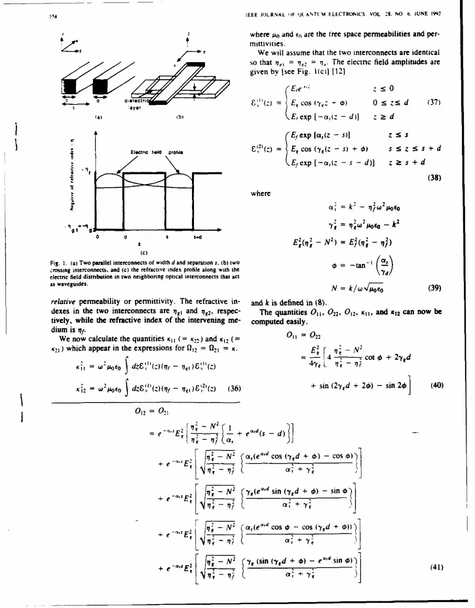
55d IEEE JOLRNAL OF Q)LANTI',M ELECTRONICS. VOL 28. NO 6. JUNE 1992
where go and e. are the free space perTneabilities and per-
mittivilles.SY We will assume that the two interconnects are identical
so that 'Y?, = 1,2 = 7. The electric field amplitudes are
given by Isee Fig. I (c) 121
( E,.e "' - - -: 0
F, d, ectri(£ (Z) = Ev cos ((,z - 0) 0 s zs d (37)S ayor
S ! •b) Ef exp [-a,(Z - d)] z a d
(Ejexp [a,(z - s)] z s S
Electric field profile E,,() " 4 cos (,, (z - s) + () s s z s s + d.E, •••• exp [-a,(z-s-d)) z 2ts+ d(8
(38)
where
r • 2
"" . 2 7 -
0 d s $12, - N2) = (i7 -
(c)
Fig. I. (a) Two palnlel interconnects of width d and separation s. (b) two (tan-'
crossing interconnects, and (c) the refractive index proile along with the (a delectric field distmbution in two neighboring optical interconnects that act
as waveguides. N k (39)
relative permeability or permittivity. The refractive itt- and k is defined in (8).dexes in the two interconnects are i1 and i1g2, respec- The quantities 011, 022, 012, 911, and 8(2 can now betively, while the refractive index of the intervening me- computed easily.dium is i7f. Oil 022
We now calculate the quantities K (= K__) and K 12 (--
K•,) which appear in the expressions for 12 = 2, = K. E2 F4/ - N 2
[4= -- 4cot 0 + 2',ydu = O 'oo d4y,,)£,(z) 4 L 7L 2; - '?I
i2, = ('0o dg'11(z)(,1, - q€1)£'(z) (36) + sin (2-yd + 20) - sin 20 (40)
012 = 021
=e-"2 _7 -5_ + e~~~ d)3j
F N N2' (cit(e Csd + co+ e -•'7E csc
++7
2 :N -N2 yg(e sin (-Vgd + 0) -sin b
_ L, a, (e od COS cos (y~d +0))
+ -E2 - i N , (sin (y; + 0)( e(si
+~ e sEI _r 1C (41)
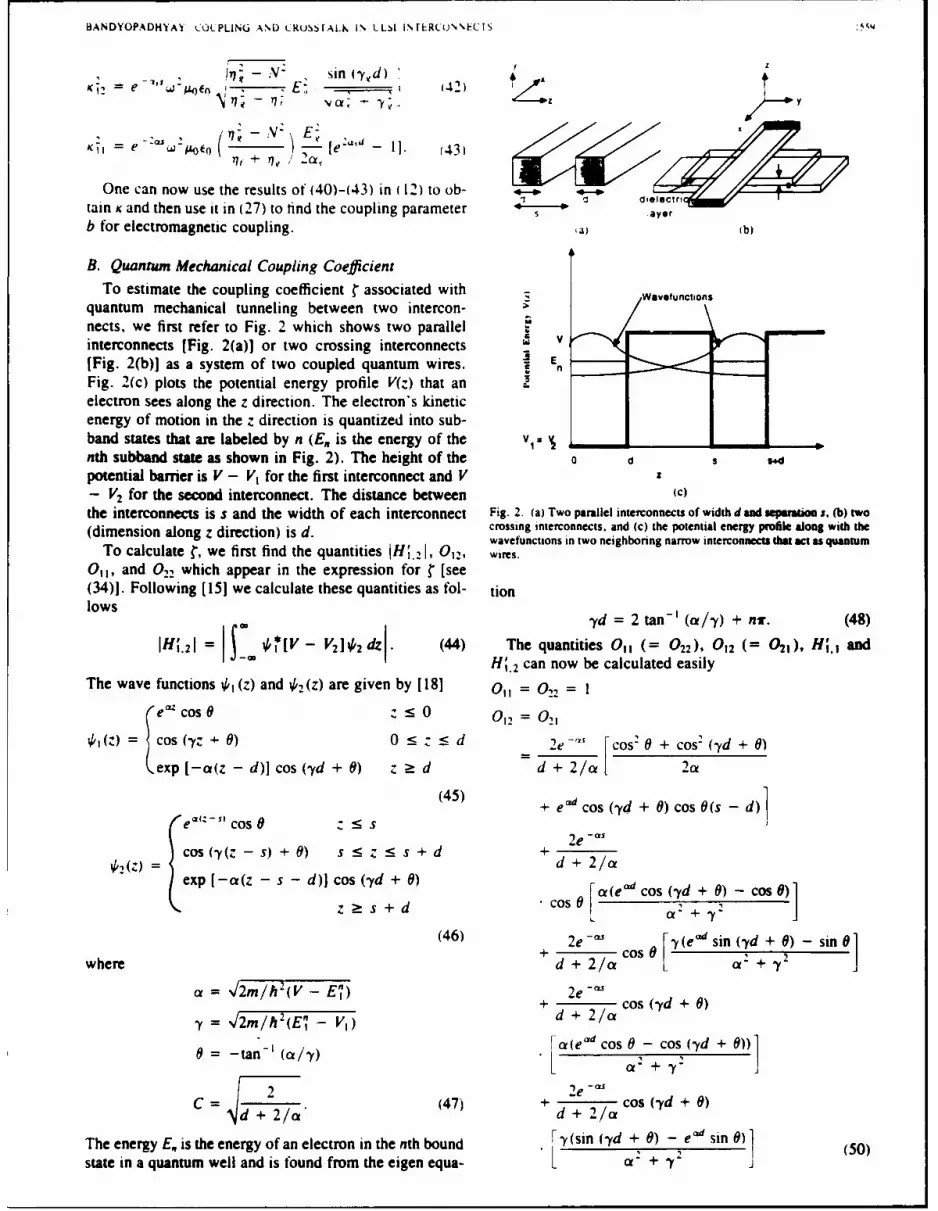
BANDYOPADHYAY CoLPLING AND LRUStIALI, IN LL•i IN•ERCONN"ECTS
sin y(,d)
N- *.E ;•h= e :a. tt ~ - - - I--e"'•' 11. 1431
K1 e+ / 243
One can now use the results of (40)-(43) in 12) to ob-I d elecit,tain x and then use it in (27) to find the coupling parameter S aye?b for electromagnetic coupling. a) (b)
B. Quantum Mechanical Coupling CoefficientTo estimate the coupling coefficient " associated with Wavefunctions
quantum mechanical tunneling between two intercon-nects, we first refer to Fig. 2 which shows two parallelinterconnects [Fig. 2(a)] or two crossing interconnects _ v
!r I[Fig. 2(b)] as a system of two coupled quantum wires. I EFig. 2(c) plots the potential energy profile V(z) that anelectron sees along the z direction. The electron's kineticenergy of motion in the z direction is quantized into sub-band states that are labeled by n (E. is the energy of the V1 • _ _
nth subband state as shown in Fig. 2). The height of the 0 d s sd
potential barrier is V - V, for the first interconnect and V- V2 for the second interconnect. The distance between (c)the interconnects is s and the width of each interconnect Fig. 2. (a) Two parallel interconnects of width d and epamitioa s. (b) two(dimension along z direction) is d. crossing interconnects, and (c) the potential energy profile along with thewavefunctions in two neighboring narrow interconnects that act as quantum
To calculate C, we first find the quantities JHI.21, 02", wire.
011, and 022 which appear in the expression for r [see(34)]. Following [151 we calculate these quantities as fol- tionlows -yd = 2 tan - (a ,y) + nu. (48)
1H;. 21 = 0 [V - V2 2 dz. (44) The quantities O, (= 022), 012 ( 021), H;. andi- H, 2 can now be calculated easily
The wave functions f, (z) and 02.(z) are given by [181 ]11 = 022
(e cCos 0 z : 0 012 = Oi2
(z) =1 cos (yz 9) 0__2e-' [cos- 0 + cos2 (-Yd + 0)
k.exp [-a(z - d)] cos (-yd + 0) z a d d + 2/a 2
(45) + e" cos ('Yd + 0) cos 6(s - d)Ie- Cos -< S
2ecos( (z- s) + 0) s 5 z :s s + d +
exp [-a - s - d) cos (yd + 0)) Cos)
z ~~ ~ ~ o 2ty + 0) o 12 .- or+ + 0,
(46) 2e- -y(ed sin (-d + 9) sin ]where d + 2/a C" + "f2
O f = V/ 2 m / 1 h 7 ( ( V _- E ) 2 e - ' -d + 0
r ae dco -Cos (-,d + 0))0= -tan-' (Cf/3,5• .aeao= I" +cs(,+0
s =te2 4n a 2e - st cie + ])
e = + 2/a' 47ind + 2/aThe e nergy E. is the energy of an electron in the nth bound F -y(sin (-,d + 0) -e'd sin 0) ]50state in a quantum well and is found from the eigen equa-[ I o + -f: (50

kE 1,A R%,.L )l A1 ANTL%' I.LECTRONICS •OL 28. NO 6. JUNE 1992
:0
1 0 L = l1cm
-1" 1 0.." 1. 0 1 0 L = I cm
i~~1 hi e v0
1 0o E_ I t%,I.,..q I •
If W SoA
1.0t
( 0 100 200 300 400 SeeSeparation in atgisrom
II. 0)
iOis)
6=) 100 0 r00 400*0[.I (a)
I,' -.,-,Im/""" •"• I
l.3.6 / 3",.,... ' v - .... U- AI
W- I014 I *Jl
If Is
W 2' IE -" ism 1
S IO SI$ IO 5 55 iS
LiugO .1 lae (gm(a
Fig 3 1a) The coupling parameter hbi 2 (which is the fraction of the power (b)in one interconnect coupled to the other) for electromagnetic coupling ver-sus the separation between the interconnects. The interconnects are I $m Fig. 4. (a) The coupling parameter Ibi 2 for quantum mechanical couplingwide and the refractive indexes of the interconnect material and the sur- versus the separation between interconnects. The istetconnects are as-roundings are 3 6 and 3 5. respectively. The results are plotted for two sumed to be made of polysilicon embedded in solicon dioxide. The energydifferent lengths of the interconnects, namely I and 10 cm. The angular barrier between polysilicon and oxide is assumed to be 3 eV, the electronfrequency is 6w x 10" rad/s. (b). The coupling parameter Ibl versus the subhead emetu is I eV below the barrier and doe I .- "1aI kinetic ea-length of the interconnect for a spacing of 1.005 sam. All other parameters erly is 10 meV. The width W of the interconnects is 50 A. The results aemare the same as in Fig. 34a). plotted for two different lengths of the interconnects, namely I and 10 cm.
(b) The coupling parameter IbI 2 versus the length of the interconnect fortwo different spacings of 100 and 150 A. All other parameters are the same
2(V - V,) cos 1-yd + 0) sin (,yd) as in Fig. 4(a).
H; e ,,.....---I (51)d -'2/c, V Io
S2(V V') Cos' (Yd + 0) :adGaAs with a refractive index of 3.5. Fig. 3(b) shows theH1, =I e , d 2/cd+ [e__,_ - 1]. coupling parameter due to electromagnetic coupling as ad + 2 / a 2a function of interconnect length when the spacing between
(52) the optical interconnects is 1.005 usm. The signal fre-quency is assumed to be 2x10 1 4 Hz which roughly corre-
We can use the results of (49)-(52) in (33)-(35) to ob- sponds to the signal frequency of a GaAs diode laser.tam the coupling parameter b in the case of quantum me- Other parameters regarding the interconnects are shownchanical coupling, in figure legends. In Fig. 4(a) we show the coupling pa-
rameter due to quantum mechanical coupling as a functionof spacing between two identical silicide interconnects
IV. RESULTS embedded in silicon dioxide. We assume that the potentialIn Fig. 3(a) we show the coupling parameter JbI 2 due barrier between silicide and silicon dioxide is 3 eV which
to optical coupling as a function of the spacing s between is close to the potential barrier between silicon and silicontwo identical optical interconnects for two different dioxide. The interconnects are assumed to be 50 A widelengths of the interconnects. The coupling parameter Ibi 2. (the limit of present-day lithographic capability). The dataas mentioned before, is the fraction of the power in one is presented for two different lengths L of the intercon-interconnect that is coupled to the other. The intercon- nects (L = I cm and L = 10 cm). In Fig. 4(b), we shownects are assumed to be I uim wide (this is of the order of the coupling parameter as a function of the length of thethe wavelength of light emitted by semiconductor lasers interconnect for two different spacings of 100 and 150 A.and light emitting diodes). the material is GaAs with a All other relevant parameters about the interconnects arerefractive index of 3.6 and the isolating medium is Al- displaced in the legend.

:i'ND'tOP-DH'•-'t OL(UPLING AN'.D k ,N,\ %LI& N .. j ;\ 1I,.RCtLUNhL Ts l'0
V. COnCLLSIUN In conclusion, we have presented a model to calculate
It is evident from the results that coupling in optical crosstalk between optical interconnects using waveguides
interconnects is not a senous problem in ULSI. This is and between narrow and closely spaced silicide intercon-
b'ecause GaAs-AIGaAs waveguides provide excellent nects embedded in dielectrics. We find that the crosstalk
confinement of the optical signal. However. quantum me- between silicide interconnects ansing from quantum me-
,:hanical tunnelng can be quite serious in siiicide dielec- chanical tunneling could be senous in ULSI circuits. Wetmcs embedded in silicon dioxide. As shown in Fig. 4(a), have also suggested some remedies for that problem.the coupling parameter IbI ' for quantum mechanical cou-pling approaches I if the spacing is 100 A. The coupling REFERENCESis always larger for a longer length of the interconnects [ H. G. Craighead. for ultrasmall structure fabn-since a larger region for coupling is provided. As shown cation." in Physics of Quantum Electron Devices. F. Capasso, Ed
in Fig. 4(b). the coupling is also larger when the spacing New York: Spnnger-Verlag, 1989.between interconnects is smaller. In Fig. 4(b), we see that 121 H. 1. Smith. K. Ismail. W. Chu. A. Yen. Y. C. Ku, M. L. Schatten-
burg, and D. A. Antoniadis. Fabncation of quantum-effect elec-the coupling oscillates with increasing length of the inter- ironic devices using x-ray nanolithography. " in Nanostructure Phys.
connect L when the spacing is small enough. This is eas- ics and Fabrication. ed. M. A. Reed and W. P. Kirk. Eds. Boston.2 = MA: Academic. 1989.ily understood from (33) which shows that Ibl =sin" A cdmc 99
131 E. E. Ehrichs. and A. L. deLozanne. �Fabricaton of nanometer fea-(EL) which is an oscillatory function in L. When the spac- lures with a scanning tunneling microscope." in Nanostnucture Phys-ing is 100 A. the coupling and s" are large enouqh that a ics and Fabrication, M. A. Reed andW. P. Kirk, Eds. Boston. MA:
of the oscillation occurs when L =6300 A. For a Academic. 1989.ernod o341 S. P. Beaumont. "Fabncation and overgrowth of quantum wires and
spacing of 150 A, the coupling and " are much smaller dots for optoelectromc applications." in Nanotructre Physics andso that a much larger length L would be required for a full Fabrication, M. A. Reed and W. P Kirk. Eds. Boston. MA: Aca-
dof the oscillation. Therefore, we doe not see the demic, 1999.period o5 th oscillation Therefof we doe in see the [51 -- "Nanofabncation and optical assessment of quantum wires andoscillation for the spacing of 150 A in Fig. 4(b). dots." in Granuiar Nanoelectronics. D. K. Ferry, J. R. Barker. and
Fig. 4 shows the quantum mechanical tunneling be- C. Jacobini, Ed., NATO AS! Seres. New York: Plenum, 1991.tween silicide interconnects can be a serious problem in 161 D. K. Fery, "Lateral surface superlanices and the future of ULSI
microelectronics.'" in Granular Nanoelectromncs, D. K. Ferry, J. R.ULSI. Tunneling, of course, can be a coherent process or Barker. and C. Jacobini. Eds. NATO ASI Series. New York:an incoherent process (phonon-assisted tunneling, for in- Plenum. 1991.stance, is incoherent) and our analysis has dealt with co- 171 J. M. Mikkelson, L. A. Hall. A. K. Malhotra, S. D. Seccombe, andM. S. Wilson. IEEE J. Solid State Circ., vol. 16, p. 542, 1981.herent tunneling only. In our analysis, we assumed that [81 S. 1. Longg said S. E. Butner. GaAs Digital Integrated Circuit Design.
the electron wavefunction is coherent over the entire width New York: McGraw Hill. 1990.
of the interconnect which is a good assumption for very [91 T. A. Fulton and G. J. Dolan. "Observation of single electron charg-ing effects in small tunnel junctions," Phys. Rev. Len., vol. 59, p.
narrow polysilicon interconnects (< 50 A wide) even at 109, 1987.room temperature and certainly below. Consequently, 1101 A. Yariv. -'Coupled mode theory for guided wave optics, " IEEEJ.tunneling may cause significant crosstalk in ULS circ s Quantum Electron.. vol. QE-9, pp. 919-933, 1973.circuits I A. Ishimani. Electromagnetic Wave Propagation. Radiation andat room temperature and at cryogenic temperatures. Since Scattering. Englewood Cliffs. NJ: Prentice Hall. 1991.many ultrafast electronic devices such as high electron 112] T. Tamlir. Ed.. Integrated Optics. New York: Springer Verlag.mobility transistors (HEMT's) or quantum coupled de- 19751
1131 A. Hardy and W. Streiter. "Coupled mode theory of parallel wave-vices utilizing resonant tunneling transistors may be con- guides," J. Lightwave Technol.. vol. LT-3. p. 1135, 1985.strained to operate at liquid nitrogen temperatures (77 K), 1141 -, "Coupled mode solutions of multiwaveguide systems." IEEE
quantum mechanical tunneling between interconnects 1J. Quantum Electron.. vol. QE-22. p. 528. 1986.115] L. Tsang and S. L. Chuang. "Improved coupled mode theory tor
could pose a serious problem at these temperatures. To reciprocal anisotropicwaveguides." J Lightwave Technol., vol. LT-
circumevent this problem, one may devise ways of de- 6. p. 304. 1988.stroving the coherence of the electron wave function. One 1161 S. L. Chuang, 'A coupled mode tormulation by reciprocity and a
"variational principle," J. Lightwave Technol.. vol. LT-5. p. 5. 1987.possibility is to impregnate the intervening dielectric iso- 1171 -, "A coupled mode theory for multiwaveguide systems satisfyinglating the interconnects with a soft magnetic material with reciprocity." J. Lighrwave Technol.. vol. LT-5. p. 174, 1987.strong spin-orbit scattering. Since spin orbit scattering is 1181 S. L. Chuang and B. Do. "'Electron states in two coupled quantum
wells-A strong coupling of modes approach." J. Appl. Phys., vol.very efficient in destroying coherence, this may inhibit 62, p. 1290. 1987.significant tunneling between neighboring interconnectsand reduce crosstalk. The other obvious way of counter-ing this problem is to use as isolating dielectrics thoseinsulators that present a large energy barrier to tunneling. Supriyo Bandyopadbysy was born in Calcutta. India. He received the
In this respect. silicon dioxide is better than silicon nitride B.Tech. in electronics and electmcal communication engineering from thesince the energy barrier to tunneling is usually larger with Indian Institute of Technology, Kharagpur. the M.S. degree in electrical
engineenng from Southern Illinois University, and the Ph.D. degree insilicon dioxide which has an energy gap of - 9 eV com- electrical engineering from Purdue University. West Lafayette. IN.
pared to - 5 eV for silicon nitride. The small energy gap From 1986 to 1987 he was a Visiting Assistant Professor at Purdue Uni-of silicon nitride may preclude its use as isolating dielec- versity. He joined the Department or Electrical Engineering. University of
Notre Dame. Notre Dame. IN. in 1987 where he is now an Associate Pro-tnc in ULSI in spite of its other attractive properties such tessor. His research interests are in quantum and hot electron transport and
as high resistance to Na diffusion. cryogenic measurements.

New high-contrast developers for poly(methyl methacrylate) resistGary H. Bemsteina)Department of Electrical Engineenng, UnWersitYv of Notre Dame. Notre Dame. Indiana 46556
Davide A. HillDepartment oj Chemical Engineering. Unwersitv of'Notre Dame. Notre Dame. Indiana 46556
Wen-Ping LiUb) CV)Centerfor Solid State Electronics Research. Arizona State University. Tempe. Arizona 85287-6206
(Received 3 October 1991: accepted for publication 8 January 1992)
New developers for poly(methyl methacrylate) consisting of mixtures of common developing >,
components have been carefully investigated. It has been found that adding a smallpercentage of methyl ethyl ketone to methyl isobutyl ketone and Cellosolve results in asignificant increase in contrast. Results of contrast experiments as well as improvements inelectron-beam lithographic exposures are reported. An explanation of the mechanism ofcontrast and resolution enhancement is offered.
I. INTRODUCTION veloper allowing the exposed pattern to be indented intothe resist. In further processing steps, the pattern is trans-
Very large scale integration (VLSI) technology con- ferred by various techniques to the substrate material. Antinues to push toward smaller geometries with advance- important limitation on the density of the exposed pattern,ment in the j Am range and experimental circuits such as and in some respects the individual line-widths is the prox-monolithic microwave integrated circuits (MMICs) in the imity effect which causes exposure of the resist up to sev-0.1 Am range. The fabrication of nanostructures and quan- eral micrometers away from the area of the primary expo-turn devices below 0.1 jAm especially relies on ultrahigh sure. As lines are placed closer together, the total doselithographic resolution, and as such continues to utilize increases between the primary exposed regions, thus lead-primarily poly(methyl methacrylate) (PMMA) as the re- ing to a decreased differential in exposure.2 The require-sist of choice. PMMA continues to find applications in ments of the developer to distinguish between differences inelectron-beam lithography (EBL), focused ion-beam li- dose become more stringent if the pattern is to be resolved.thography, x-ray lithography, deep uv optical lithography, Ideally, a developer will remove all positive resist thatand, more recently, scanning tunneling lithography., It is has been exposed to a dose above a certain threshold andalmost universaly the choice for the development of new none of the resist that has been exposed below that thresh-lithographic techniques since PMMA offers the highest old. In practice, a range of exposures results in partialknown resolution of any organic resist. A drawback to the development of the resist over that range. For this reason,use of PMMA is that it is generally not sensitive enough higher contrasts allow a narrower area to be developedfor manufacturing purposes, but it does offer extremely completely even in the presence of those factors thathigh resolution. For this reason, PMMA remains techno- broaden the exposure. For other lithography schemes men-logically important. tioned above, similar energy scattering limitations to reso-
The generally accepted criterion of resolution predic- lution exist. It is expected that for all types of lithography,tion of a resist-developer system has fallen on contrast y. higher resolution will result from higher contrast, and theHigh contrast can be thought of as the ability of a devel- improvements discussed below will be equally relevant tooper to discriminate between very small differences in ex- any application of PMMA.posure dose from one small area to an adjoining one. Ex- Contrast is a measure of the sharpness of the develop-posure in electron-beam lithography is not precisely ing threshold of the developer-resist system and is definedlocalized due to factors including the Gaussian beam cross as the slope of the plot of normalized thickness of the resistsection, forward scattering in the resist, backscattering remaining after development versus the logarithm of thefrom the resist and substrate (proximity effect), and the exposure dose. Figure 1 illustrates the definition of y. Thegeneration of secondary electrons in the resist. 2 These fac- onset of development D, is defined to be the dose at thetors decrease the modulation transfer function of the ex- intersection of the steepest part df the contrast curve ex-posure for closely spaced patterns. trapolated to the 100% level of the curve. The sensitivity
In PMMA, a positive resist, bonds are broken by inci- Df is defined to be the dose of the extrapolated curve atdent radiation (e.g., an electron beam), decreasing the av- zero thickness.erage molecular weight M of the long-chain molecules. As discussed above, y is a measure of the ability of theThis increases the solubility of the resist in a suitable de- developer to distinguish between gradations of dose. Since
contrast is expressed as
".Author to whom correspondence should be addressed."Present Addrew VLSI Research Department. Lashan Microelectronics
Co.. P.O. Boa 19. lUitons, Shaanxi 710600. Peoples Republic of China. y [log(Dl/Df)] - K (1)
4066 J. Appl. Phys. 71 (8), 15 April 1992 0021-8979/92/084066-10504.00 !D 1992 American Institute of Physics 4066

subts. Some of our developer solutions give improvementsof up to 35% in contrast and no loss in sensitivity.
Three chemical solutions are often employed asSPMMA developers. These are (i) methyl ethyl ketone:eth-
anol (EtOH) in a ratio of 26.5:73.5: (ii) Cellosolve (2-
ethoxvethanol):methanol (MeOH) in a ratio of 3:7: and(iii) methyl isobutyl ketone:2-propanol (IPA) in a ratio of1:3. These solutions are referred to here simply as solutionA. or S-A, solution B. or S-B, and solution C, or S-C,
(D respectively. Pure methyl ethyl ketone, Cellosolve, and me--E thyl isobutyl ketone will be represented by MEK, CS, andE MIBK, respectively. S-C has been reported to provide veryz high resolution at exposures of 50 kV electrons with a
development time of 15-45 s"1-'2 while S-B has been re-Di Df log Dose ported to provide very high resolution in EBL exposures
between 20 and 120 kV with a development time of 5 L13.14
FIG. I. Plot of normalized positive resist thickness remaining after de- It is mixtures of these three common developer solutionsvelopment as a function of log of exposure dose (the contrast curve) which we have found to give markedly improved results inillustrating the deinitions of D, and D/. contrast.
II. EXPERIMENT
For resist exposures, we used an ISI-100B scanninga higher absolute value of y represents a higher contrast electron microscope (SEM) modified for EBL in a vector-developer. (In this report, the absolute value of all contrast scanned mode with an exposure spot (pixel) spacing mdvalues will be used, but are all negative.) The ideal situa- beam diameter of 100 rnm each.' 5 All test exposures weretion discussed above in which there is an absolute dose performed at 40 kV on thick silicon substrates. All PMMAthreshold for dissolution represents an infinite contrast, films were of molecular weight 950 000 a.u., spin coatedwhereas in practice the contrast is always finite. Contrast is and baked at 160 "C for 4 h, with resist thicknesses ranging
commonly measured experimentally for a given develop- from 0.4 to 1.0 14m. Exposures were arranged in a 6X6
ment time by varying the exposure dose in small incre- array of 50X 50 jm 2 squares. Resist thicknesses remaining
ments through the region of dose that causes the resist to after development were obtained using a Dektak II surface
dissolve until total dissolution is achieved. A common profilometer.
method for measuring r is to use a surface profilometer to S-A, S-B, and S-C were tested alone and in combina-
measure the thickness of resist remaining after exposure using development times that yieled approximately
and development and plot the data as discussed above.3- 9 the same dose for complete development and also corre-As we discuss later, the contrast parameter is entirely sponded to typical values from the literature. These timesAsta ed iscuss lat the dissocutontrasteh aioraether inlyer a were 45 s for S-C,"11 2 5 s for S-B,13.14 and 2 s for S-A. The
dictated by the dissolution behavior of the polymer. Pa- development time for almost all mixtures of these compo-panu et al. have produced valuable fundamental work on nents was 10 s. This time was based upon the relativethe mechanism of PMMA dissolution in one- and two- strength and concentrations of the components used in thesolvent developers, and for different polymer molecular mixtures and was estimated initially to yield the same timeweights.' 0 Their experiments greatly clarify the role of to complete development for approximately similar doses.thermodynamic quality of the solvent on the rate and The range of developer temperatures represents commonmechanism of polymer dissolution, but only for one- and fluctuations caused by varying room conditions, evapora-two-component developer mixtures. Here we approach the tive cooling, etc.more complex case of a multicomponent developer and, on Development was performed by holding the samplesmore practical grounds, we study the effect of solvent qual- with tweezers and dipping in the developer with light agi-ity (in our case various mixtures) on the rate of dissolution tation for the required time. Temperatures during develop-of electron-beam-exposed PMMA resists. We explore com- ment were determined by inserting a mercury-bulb ther-binations of common developers to ascertain whether or mometer, calibrated to I *C, into the beaker. Developernot improvements in the lithographic process could be pro- times were controlled as much as possible by careful atten-moted simply by using readily available mixtures of sol- tion to the process. Significant error occurred only in thevents. possible case of S-A with a 2 s develop (estimated at less
These new developer solutions are mixtures of chemi- than 20%), but this data was used only for crude compar-cals that have been commonly employed individually as ison as will be discussed below. All samples were rinsed fordevelopers for PMMA, but which when combined exhibit 15 s in MeOH immediately after development and blownhigher performance than when alone. Our combination of dry in nitrogen.these chemicals has shown improvements in achievable The unexposed dissolution properties of the three de-contrast of PMMA as well as improved lithographic re- veloper components were tested to ensure that normalized
4067 J. Appl. Phys., Vol. 71, No. 8, 15 Aprnl 1992 Bernstein, Hil, Wnd Liu 4067
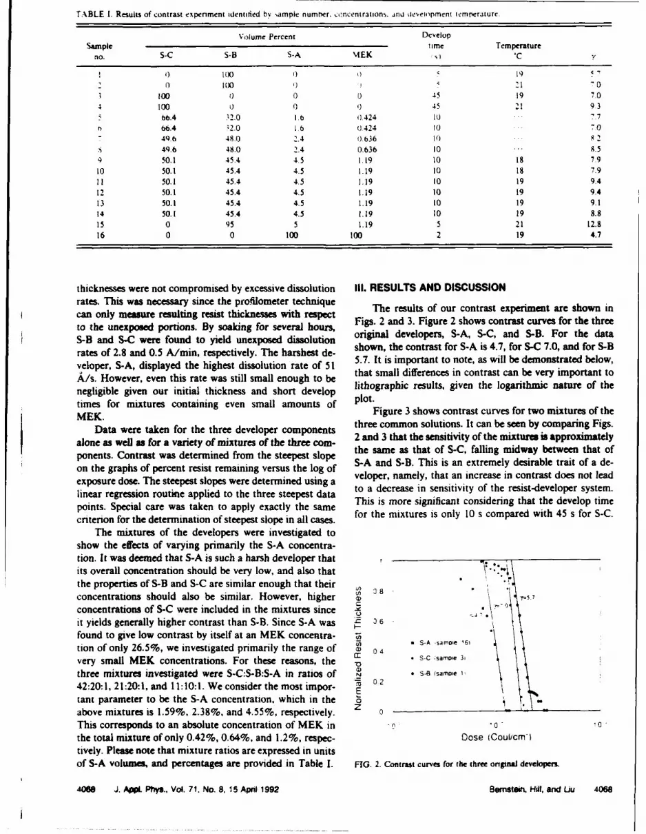
TABLE I. Results of contrast experiment identified by ,ample numner. c'ncentrations. anU development tcmr'rature.
Volume Percent DevelopSample time Temperature
no. S-C S-B S-A MEK C
101003 0 9)5t -
0 100 o) - 21 -0100 0 0 0 15 19 70
4 100 3 0 ) 45 21 9.366.4 32.0 o 0.424 10 77
66.4 32.0 1.6 0424 t0 70"49.6 48.0 2.4 0.636 10 ... 8 2
49.6 48.0 2.4 0.636 10 8.550.1 45.4 4.5 1.19 10 18 7.9
10 50.1 45.4 4.5 1.19 10 18 7.9
I1 50.1 45.4 4.5 1,19 10 19 9.4
12 50.1 45.4 4.5 1.19 10 19 9.413 50.1 45.4 4.5 1.19 10 19 9.114 50.1 45.4 4.5 1.19 10 19 8.815 0 95 5 1.19 5 21 12.8
16 0 0 100 100 2 19 4.7
thicknesses were not compromised by excessive dissolution III. RESULTS AND DISCUSSIONrates. This was necessary since the proflometer technique The results of our contrast experiment are shown incan only measure resulting resist thicknesses with respectto the unexposed portions. By soaking for several hours, Figs. 2 and 3. Figure 2 shows contrast curves for the threeS-B and S-C were found to yield unexposed dissolution original developers, S-A, S-C, and S-B. For the datarates of 2.8 and 0.5 A/mn, respectively. The harshest de- shown, the contrast for S-A is 4.7, for S-C 7.0, and for S-Bratesopf, S-A, displayd th5A/minrespectve l. hihest dia e -o5.7. It is important to note, as will be demonstrated below,veloper, S-A , displayed the highest dissolution rate of 51 th t s al d fe nc si co r st an b v ry mp t nt o&/s.Howver evn tis atewas til smll nouh t be that small differences in contrast can be very important toA./s. However, even this rate was still small enough to be lihgaicrstgvetelortmcntueftenegligible given our initial thickness and short develop lithographic results, given the logarithmic nature of thetimes for mixtures containing even small amounts of plot.MEK. Figure 3 shows contrast curves for two mixtures of the
Data were taken for the three developer components three common solutions. It can be seen by comparing Figs.
alone as well as for a variety of mixtures of the three com- 2 and 3 that the sensitivity of the mixtures is approximately.Contrast was determined from the steepest slope the same as that of S-C, falling midway between that of
on the graphs of percent resist remaining versus the log of S-A and S-B. This is an extremely desirable trait of a de-
exposure dose. The steepest slopes were determined using a veloper, namely, that an increase in contrast does not lead
linear regression routine applied to the three steepest data to a decrease in sensitivity of the resist-developer system.
points. Special care was taken to apply exactly the same This is more significant considering that the develop time
criterion for the determination of steepest slope in all cases. for the mixtures is only 10 s compared with 45 s for S-C.
The mixtures of the developers were investigated toshow the effects of varying primarily the S-A concentra-tion. It was deemed that S-A is such a harsh developer thatits overall concentration should be very low, and also thatthe properties of S-B and S-C are similar enough that theirconcentrations should also be similar. However, higher 5,7
concentrations of S-C were included in the mixtures since -7
it yields generally higher contrast than S-B. Since S-A was 3 • 6found to give low contrast by itself at an MEK concentra- "
a S-A .samowe '61tion of only 26.5%, we investigated primarily the range of 04
very small MEK concentrations. For these reasons, the a: * S.C samoe 3
three mixtures investigated were S-C:S-B:S-A in ratios of - S-6 samole-• 02
42:20:1, 21:20:1, and 11:10:1. We consider the most impor- E
tant parameter to be the S-A concentration, which in the 0above mixtures is 1.59%, 2.38%, and 4.55%, respectively. z 0This corresponds to an absolute concentration of MEK in .0 "0the total mixture of only 0.42%, 0.64%, and 1.2%, respec- Dose (Coul/cm-1tively. Please note that mixture ratios are expressed in unitsof S-A volumes, and percentages are provided in Table I. FIG. 2. Contrast curves for the three onginal developers.
4008 J. Appl. Phys.. Vol. 71. No. 8. 15 Apnl 1992 Bemstein. Hill, and Liu 4068
T08C
- 06
S04 -SN o 21:20:1 (safTf e 7) 7 =1 :
E- a I1I"10 11 Sarntlie 11) "Y- 4
0 -
10, 10' 10___Dose (Coul/cm-1 (a)
FIG. 3. Contrast curves for mixtures of the original developer compo-nents. Ratios are S-C:S-B:S-A.
This implies that the mixture must offer higher sensitivitythan S-C or S-B alone if development times are increased.In addition, it is shown in Appendix A that contrast ispredicted to increase for increased develop times but onlyfor an increased solubility, as in our case of added MEK.This implies that further study would indicate a possibilityof achieving even higher contrasts coupled with improvedsensitivity for longer develop times. In practice, the opti- Lmum exposures for highest resolution correspond to the tb)dose at Df of Fig. 1, where Df must decrease for increaseddevelop time. This has strong implications for the viability FIG. 4. Photomicrographs of test patterns illustrating improved contrast
of improving the throughput of processes utilizing PMMA from new developers. The test patterns consist of parallel lines of decreas-
for high-resolution commercial applications. ing pitch in the outward directions, crossing in a variable-pitch grid pat-
We have observed markedly improved lithographic tern at the corner. Light areas indicate severe loss of resist between theexposed lines. Both patterns were exposed under identical conditions, butperformance using the new developer mixtures. Figure 4 developed by (a) S-C for 45 s and (b) S-C:S-B:S-A I I:10:1 for l0 s. The
shows photomicrographs of test patterns consisting of sets appearance of less light area in (b) implies that the mixture has provided
of parallel lines of decreasing pitch to 0. 1 pm in the direc- much higher contrast than that of S-C in (a).
tion of the outside of the pattern, and overlapping to forma variable-spaced grid in the corner. Both test patternswere exposed on a single sample under the identical con- simple matter of sensitivity and overdeveloped exposure.ditions of resist thickness, bake temperature, bake time, since the sensitivity of the 11:10: 1 mixture is almost exactlydose, line spacing, and beam energy. After exposure the the same as that of S-C as can be seen by comparing Figs.patterns were separated and developed as discussed above 2 and 3.using S-C for pattern 4(a) and S-C:S-B:S-A 11:10:1 for Figure 5(a) shows a grid pattern developed by the S-Bpattern 4(b). solution. The linewidths vary by about 25% toward the
The resulting improved contrast can be observed from interior of the pattern. Figure 5(b) shows a pattern devel-the variations in light and dark areas. One expects that as oped in S-C:S-B:S-A 11:10:1. There is almost no evidencethe parallel lines are exposed closer together, the proximity of linewidth variations over the pattern due to the highereffects cause some exposure of the spaces between the contrast of the 11:10:1 mixture versus that of the S-B. Inlines.2 A lower-contrast developer will dissolve the PMMA addition, lift-off properties are affected by contrast. Figureat the lines of exposure and also remove much of th... resist 5(a) shows a typical example of metal flakes left from thebetween the lines. This is the cause of the light areas in Fig. unexposed areas after a lift-off step in acetone. Figure 5(b).4(a) as the line pitch decreases. However. a sufficiently however, shows the consistentl% improved lift-off achievedhigher-contrast developer will remove mostly the resist in due to steeper sidewalls resulting from the higher contrast.areas of direct exposure and less of the resist between the The patterns, of Figs. 4 and 5. then, help demonstrate thatlines. This is the case in Fig. 4(b) where there is clearlN the new m-xtures provide usably higher contrast comparedless light area, showing that the resist remains intact be- with conventional developerstween the lines even in the presence of identical proximit. Table I shows the contrast for various percentages ofeffects to part 4(a). These results cannot be explained as a developer solutions and temperatures. A plot of contrast as
4069 J. Appi. Phys., Vol. 71. No. 8. 15 April 1992 5ernstein, Hill. and Liu 4069

14,Aim A MIXTURES
0 S-C 15 (21°C) A
12' m S-B
1011.12 (19C) A4 (21°C) 13 (19"C) *
t 7 14 (19C)
8- 1 A 5 9.10 (18°C) AS3 (19*rC) 6
"2 (210C)
6-1 (19°C)
0.0 0.2 0.4 06 08 1.0 1.2 14
Jim %M13<
FIG. 6. Plot of y as a function of percent MEK, uncorrected for temper-ature dependence. Sample number and temperature are noted for eachdatum.
about a 1.3% increase of MEK concentration in the mix-ture results in more than a 35% increase in contrast, andthat further improvements can be promoted by simply in-creasing the temperature.
The fact that S-B does not fall on the temperature-4b) compensated line can be qualitatively understood by noting
FIG. 5. Grid patterns formed by EBL exposure at 40 kV on GaAs sub-strates followed by development and lift-off of 40 nm gold: (a) developed-i S-B and (b) developed in S-C:S-B:S-A 11:10:1. Note decreased linebroadening in (b) vs (a) indicating higher contrast of the mixture over 14S-B. Also note typical improved lift-off as a result of steeper edge profilesdue to higher contrast.
12
a function of percent S-A, uncorrected for temperaturedependence, is shown in Fig. 6. A tren.3 of increasing y as iS-A is increased is indicated. The same data, but normal- 0 10 -. 15
ized to 19 "C, are shown in Fig. 7. (Note that contrast data 7.8
sho%: qo correlation with the initial resist thickness, which 5.6'ý 8is accounted for in the process of normalizing the remain- E 3.4
ing thickness after development.) The temperature nor- Z A A 0 45°c
malization assumes an Arrhenius behavior with an activa-tion energy of 24.3 kcal/mol, found by fitting contrast data 1,2
at a fixed S-A percentage as a function of temperature. Thisvalue is intermediate between that found by Cooper. Kra-sicky, and Rodriguez 16 of 25 kcal/mol for MEK and that 0.0 0,2 0 4 0 6 0 8 1 0 1 2 14
reported by Greeneich17 of 24 kcal/mol for MIBK. In thecase of Fig. 7, a trend of increasing contrast for increasing %MEJpercent MEK is ,'-w clearly evident. The data. includingS-C, collapse to a straight line of the least-squares fit very FIG. 7. Plot of y as a function of percent MEK. corrected for temperature
dependence by normalizing to I1'C The normalization assumes anclosely except for the case of S-B at 01 MEK. (Precise Arrhenius dependence with an activation energy of 24.3 kcal/mol Noticetemperatures were not available for the case of 0.42% and that the points in Fig 6 corresponding to sample no 4 (21 *C) for pure
0.64% MEK. The bar in the figure is not an error bar, but S-C and that of samples no. 9 and 10 (18 C) at 1.19% MEK have
represents calculated uncertainty of plus or minus 0.45 'C collapsed onto the straight line and are now obscured on the graph h."other data points. The bar in the figure is not an error bar, but represents
based on the known value of the activation energy centered calculated uncertainty of ±0.45 'C based on the known value of theabout 19 C.) It is striking that within this linear region, activation energy centered about 19 C
4070 J. Appi. Phys.. Vol. 71. No 8. 15 April 1992 Bernstein, Hill. and Liu 4070

that both MEK and MIBK are ketones, while CS (2- FABLE 11. Molecular weight and solubility parameters for each compo-
ethoxyethanol) contains both alcohol and ether groups. ,ient of the mixtures. The distance , is included for each component.
The chemical compositions of MIBK and MEK are verysimilar, differing only by two aliphatic carbons. In order to o
understand the dynamics completely, one would need to
consider a full thermodynamic and transport analysis in- MEK 72 140 4 3 9 5 1.4
volving six components. A complete analysis is beyond the EtOH 46 12.6 1,2 20.0 12MIBK 100 14.4 8.1 5.9 3.4
scope of this work. but a simple explanation of the role of IPA 0 14.0 4 8 16.0 7.5
the components is given below. cs 90 13.0 Q 1 15.2 6.8
Previous analyses of the development of EBL-exposed MeOH 32 11.6 13.0 24.0 16
resist show that measured decrements of normalized resist MMA 90 13.5 10.1 8.5 ...
thickness upon exposure (i.e., the contrast curve) shouldbe directly proportional to the rate of polymer dissolution' 7 parameter space, A is the distance between the end points(see also Appendix A). For a given developer system, this of these vectors. We therefore refer to A as simply "dis-rate depends on the average molecular weight of the ex- tance."posed polymer, which in turn is a function of the dose. It is expected that the greater the distance A is, thenAppendix A shows that contrast is expected to exhibit the the less efficient the component is at dissolving PMMA,same temperature behavior as that of dissolution rate and and therefore the lower is the solvent quality. Such mea-explains our observation of increased y for developments sure of compatibility is consistent with the idea that polar,performed at slightly higher temperatures where dissolu- dispersive, and hydrogen-bonding forces can, in principle,tion rates are in general higher. We found that at all S-A act independently. (For example, two chemical species,concentrations, y increased with temperature between 18 one strongly polar but nonhydrogen bonding, and theand 21 'C. With the exception of only the S-B data, all other weakly polar but strongly hydrogen bonding, couldother data properly collapsed onto the best-fit line as a have the same global solubility parameter and yet be im-function of temperature as suggested by the above theory. miscible. This is the same as saying that the length of 8, in
The main factors that affect the rate of solubilization of solubility space is the same for each species, but their di-a polymer in a solvent are the plasticization and thermo- rections vary greatly.) Thus only those solubility parame-dynamic compatibility, or solvent "quality." Plasticization ter components pertaining to congruent energetic interac-refers to the ability of the solvent to penetrate the polymer tions should be compared.and increase the free volume,' 8 19 making it more vulnera- The calculated values of A for all pure solvents com-ble to dissolution. The rate at which a solvent can plasticize pared with MMA, along with the molecular weights ofa polymer is related to its molecular size and therefore its each component, are given in Table 1I. Again, the plasti-molecular weight. Gipstein et aL20 reported a noticeable cization, or molecular weight, of the individual compo-solvent-size effect in the dissolution rate of atactic PMMA nents must also be considered in explaining their role in thein a homologous series of n-alkyl acetates. They found a solutions. Table III indicates the order of each developerprecipitous drop in dissolution rate for increased penetrant component in its ranking of plasticization and solvent qual-molecular weight. As an approximation we will use molec- ity. We can see that MEK is indeed the best solvent butular weights as an estimator of the relative ability of the rates fourth as a plasticizer. In S-A, the EtOH serves as asolvent components to plasticize the exposed PMMA. diluent and to help in plasticization, being ranked second
The solvent quality is related to the match between in this regard. These two facts help to explain why S-A isthree thermodynamic parameters of the solvent and the such an effective solvent of PMMA at 3060 A/min for apolymer. The closer these are, the higher is the thermody- molecular weight as high as 950 000 a.u. This also helps tonamic compatibility resulting in a higher dissolution rate.19 explain why S-A exhibits the worst contrast, since itThese parameters are the three components of the global strongly dissolves PM-MA of all molecular weights. Al-solubility parameter 6, namely the dispersive, polar, and though CS ranks third in solvent quality, it appears thathydrogen-bonding components, 6d, 6p, and 6h, respectively, the presence of MeOH in S-B, ranked first for plasticiza-where tion, helps to increase the effectiveness of CS as a solvent.
Regarding S-C dissolution, the component MIBK is rated8p +6h +8d.(2)
TABLE 1I1. Ranking of plasticization and solvent quality for each com-ponent of the developer solutions.
We have found it useful to compare all of these com- _ponentofthedevelopersolutions.
ponents in an attempt to explain our results. In comparing MEK EtOH MIBK IPA CS MeOH
the similarity of the three solubility parameters between Distancethe developers and PMMA, we have defined the parameter a [(MPa)"'2 1 1.4 12 3.4 7.5 6.8 16
M (g/mol) 72 46 100 60 90 32
A [(p, - 6)2 ..a- (6h, _- 6h)2 + (bdi _- 6d.)21 I/2 (3) Solvent quality I 5 2 4 3 6i rankk)
Plasticization 4 2 6 3 1where i indicates a developer component and j the resist. (rank)Since 6, is the lengt'- of the solubility vector in solubility
4071 J. AppI. Ptiys., Vol. 71. No. 8, 15 April 1992 Bemstein. Hill, and Liu 4071
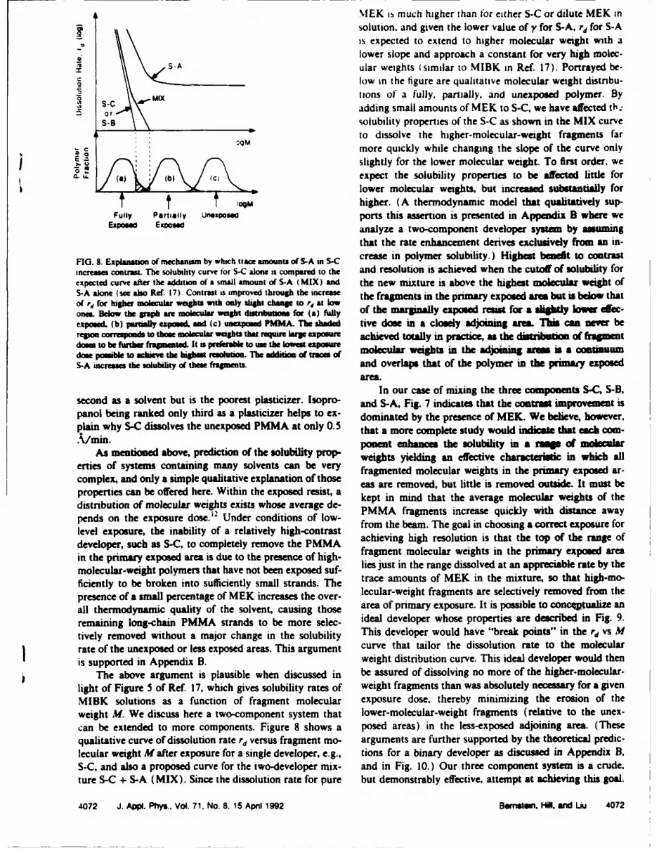
N4EK is much higher than for either S-C or dilute MEK insolution. and given the lower value of y for S-A. rd for S-Ais expected to extend to higher molecular weight with a
SA lower slope and approach a constant for very high molec-. .-A ular weights (similar to MIBK in Ref. 17). Portrayed be-o low in the figure are qualitative molecular weight distnbu-
"•Mix tons of a fully, partially, and unexposed polymer. By
- or adding small amounts of MEK to S-C, we have affected th-S.s solubility properties of the S-C as shown in the MIX curve
to dissolve the higher-molecular-weight fragments farmore quickly while changing the slope of the curve onlyslightly for the lower molecular weight. To first order. we
. (a) (b) (c expect the solubility properties to be affected little forlower molecular weights, but increased substantiaUy for
'l9oMu higher. (A thermodynamic model that qualitatively sup-Fully Partially Unexposed ports this assertion is presented in Appendix B where we
Exposd Exposed analyze a two-component developer system by .mumig
that the rate enhancement derives exclusively from an in-
FIG. 8. Explanation of mechanusm by which trace amounts of S-A in S-C crease in polymer solubility.) Highest bat to contrast
increases contrast. The solubility curve for S-C alone is compared to the and resolution is achieved when the cutoff of solubility forexpected curve after the addition of a small amount of S-A (MIX) and the new mixture is above the highest molecular weight ofS-A alone (see also Ref. 17). Contrast is improved through the increase the fragments in the primary exposed arm but is below thatof rd for highe molecular weights with only sight change to rd At lowones. Below the grah are molecular weight distnbutm for (a) fully of the marginally exposed resist for a slightly lower effec-exposed. (b) painally exposed, and (c) unexpomed PMMA. The shaded tive dose in a closely adjoining ares. This can never beregion correspomnd to thost moleculat weights that reqme large exposure achieved totaly in practice, as the distribition of fragmentdoam to be fiuther fhaimmted. It a ptferable to use the lowesit Sepom molecular weights in the adjoining ari is a continuumdome pomable to achieve the hig resolutwin. Te addiion of tram ofS-A increases the solubility of tse fraents, and overlaps that of the polymer in the primay exposed
area.
In our case of mixing the three components S-C, S-B,second as a solvent but is the poorest plasticizer. Isopro- and S-A, Fig. 7 indicates that the contrast improvement ispanol being ranked only third as a plasticizer helps to ex- dominated by the presence of MEK. We believe, however,plain why S-C dissolves the unexposed PMMA at only 0.5 that a more complete study would indicate that each com-./min. ponent enhances the solubility in a rmp of molecular
As mentioned above, prediction of the solubility prop- weights yielding an effective characteritic in which allerties of systems containing many solvents can be very fragmented molecular weights in the primary exposed ar-complex, and only a simple qualitative explanation of those fragaentemoleculits in the primar exposeeas are removed, but little is removed outside. It must beproperties can be offered here. Within the exposed resist, a kept in mind that the average molecular weights of thedistribution of molecular weights exists whose average de- PMMA fragments increase quickly with distance awaypends on the exposure dose.12 Under conditions of low- fr am ents incrase qui c t distn e awalevel exposure, the inability of a relatively high-contrast from the beam. The goal in choosing a correct exposure fordeveloper, such as S-C, to completely remove the PMMA achieving high resolution is that the top of the range ofin the primary exposed area is due to the presence of high- fragment molecular weights in the primary exposed areamolecular-weight polymers that have not been exposed suf- lies just in the range dissolved at an appreciable rate by theficiently to be broken into sufficiently small strands. The trace amounts of MEK in the mixture, so that high-mo-presence of a small percentage of MEK increases the over- lecular-weight fragments are selectively removed from theall thermodynamic quality of the solvent, causing those area of primary exposure. It is possible to concepualize anremaining long-chain PMMA strands to be more selec- ideal developer whose properties are described in Fig. 9.
tively removed without a major change in the solubility This developer would have "break points" in the rd vs M
rate of the unexposed or less exposed areas. This argument curve that tailor the dissolution rate to the molecular
is supported in Appendix B. weight distribution curve. This ideal developer would then
The above argument is plausible when discussed in be assured of dissolving no more of the higher-molecular-
light of Figure 5 of Ref. 17, which gives solubility rates of weight fragments than was absolutely necessary for a given
MIBK solutions as a function of fragment molecular exposure dose, thereby minimizing the erosion of the
weight M. We discuss here a two-component system that lower-molecular-weight fragments (relative to the unex-
can be extended to more components. Figure 8 shows a posed areas) in the less-exposed adjoining area. (These
qualitative curve of dissolution rate rd versus fragment mo- arguments are further supported by the theoretical predic-lecular weight M after exposure for a single developer, e.g., tions for a binary developer as discussed in Appendix B.S-C, and also a proposed curve for the two-developer mix- and in Fig. 10.) Our three component system is a crude,ture S-C + S-A (MIX). Since the dissolution rate for pure but demonstrably effective, attempt at achieving this goal.
4072 J. Appl. Phys., Vol. 71, No. 8. 15 AprI 1992 Bernstsn. Hill, and Liu 4072
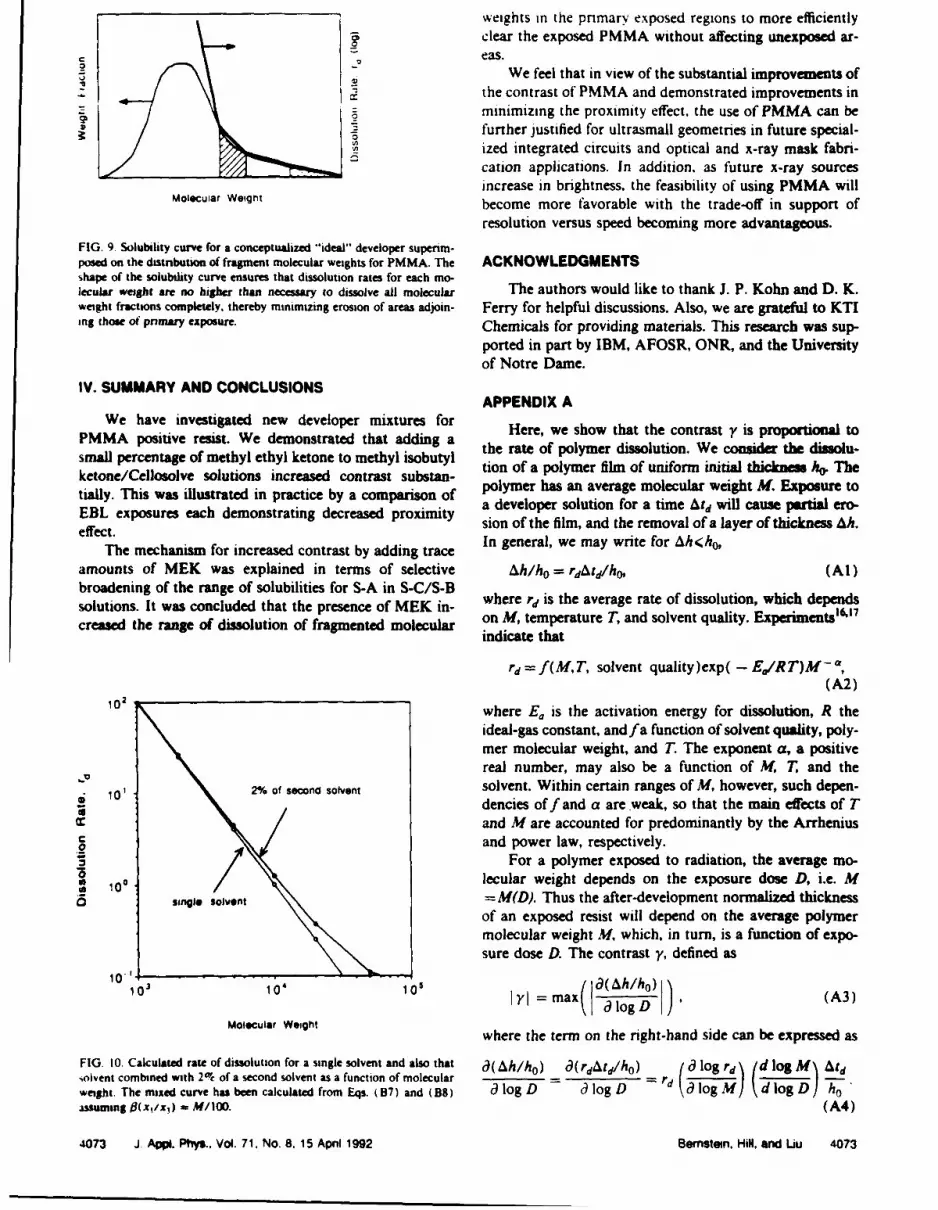
weights in the primary exposed regions to more efficiently_• clear the exposed PMMA without affecting unexposed ar-
eas.We feel that in view of the substantial improvements of
the contrast of PMMA and demonstrated improvements inminimizing the proximity effect, the use of PMMA can befurther justified for ultrasmall geometries in future special-ized integrated circuits and optical and x-ray mask fabri-cation applications. In addition. as future x-ray sourcesincrease in brightness. the feasibility of using PMMA will
moiecuiar weight become more favorable with the trade-off in support ofresolution versus speed becoming more advantageous.
FIG. 9 Solubility curve for a conceptualized"ideal" developer superim-posed on the dstnibuton of fragment molecular weights for PMMA. The ACKNOWLEDGMENTSshape of the solubility curve ensures that dissolution rates for each mo-lecular weight are no higher than necessary to dissolve all molecular The authors would like to thank J. P. Kohn and D. K.weight fractions completely, thereby minimizing erosion of areas adjoin- Ferry for helpful discussions. Also, we are grateful to KTIing those of pnmary exposure. Chemicals for providing materials. This research was sup-
ported in part by IBM, AFOSR, ONR, and the Universityof Notre Dame.
IV. SUMMARY AND CONCLUSIONSAPPENDIX A
We have investigated new developer mixtures for Here, we show that the contrast y is proportional toPMMA positive resist. We demonstrated that adding a the rate of polymer dissolution. We consider the diuuolu-small percentage of methyl ethyl ketone to methyl isobutyl thra of polymer filmouniorm ini the d Theketone/Cellosolve solutions increased contrast substan- tion of a polymer film of uniform initial thckExss u Thetially. This was illustrated in practice by a comparison of polymer has an average moleular weight cMa. Eaxpsure toEBL xpoureseac demnstatig dereaed poxiity a developier solution for a time At~d will cause pata er'o-EBL exposures each demonstrating decreased proximity sion of the film, and the removal of a layer of thickness Ah.effect. In general, we may write for Ah<ho,
The mechanism for increased contrast by adding traceamounts of MEK was explained in terms of selective Ah/ho = rdAtdl/h, (Al)broadening of the range of solubilities for S-A in S-C/S-B where rd is the average rate of dissolution, which dependssolutions. It was concluded that the presence of MEK in- on M, temp era ge rand sol ut whity dependscreased the range of dissolution of fragmented molecular on dMi, temperature T, and solvent quality. Experiments'6' 7
indicate that
rd = f(M,7T, solvent quality)exp( - E.IRT)M ,(A2)
102 where Ea is the activation energy for dissolution, R the
ideal-gas constant, andfa function of solvent quality, poly-mer molecular weight, and T. The exponent a, a positivereal number, may also be a function of X, T, and the
10 2%1. of second solvent solvent. Within certain ranges of M, however, such depen-Sdencies of f and a are weak, so that the main effects of Tand M are accounted for predominantly by the Arrhenius
0 and power law, respectively._/ For a polymer exposed to radiation, the average mo-
S 100 lecular weight depends on the exposure dose D, i.e. M0. 100
si ngl solvent = M(D). Thus the after-development normalized thicknessof an exposed resist will depend on the average polymermolecular weight M, which, in turn, is a function of expo-sure dose D. The contrast y, defined as
10"'I
101 0' 10s 1=max (Ah/h )WAdl logDMolecular Weight where the term on the right-hand side can be expressed as
FIG. 10. Calculated rate of dissolution for a single solvent and also that a(Ah/ho) L((rdAtd/ho) (a log rd d log M AtdNolvent combined with 2% of a second solvent as a function of molecular - D rd .odlogD ho
weight. The mixed curve has been calculated from Eqs. (B7) and (BS) 8 log D 8 log Dlog M)assuming O(x,lx,) = M/100. (A4)
4073 J. Appi. Phys., Vol. 71, No. 8, 15 Apnl 1992 Bernstein, Hill, n Liu 4073
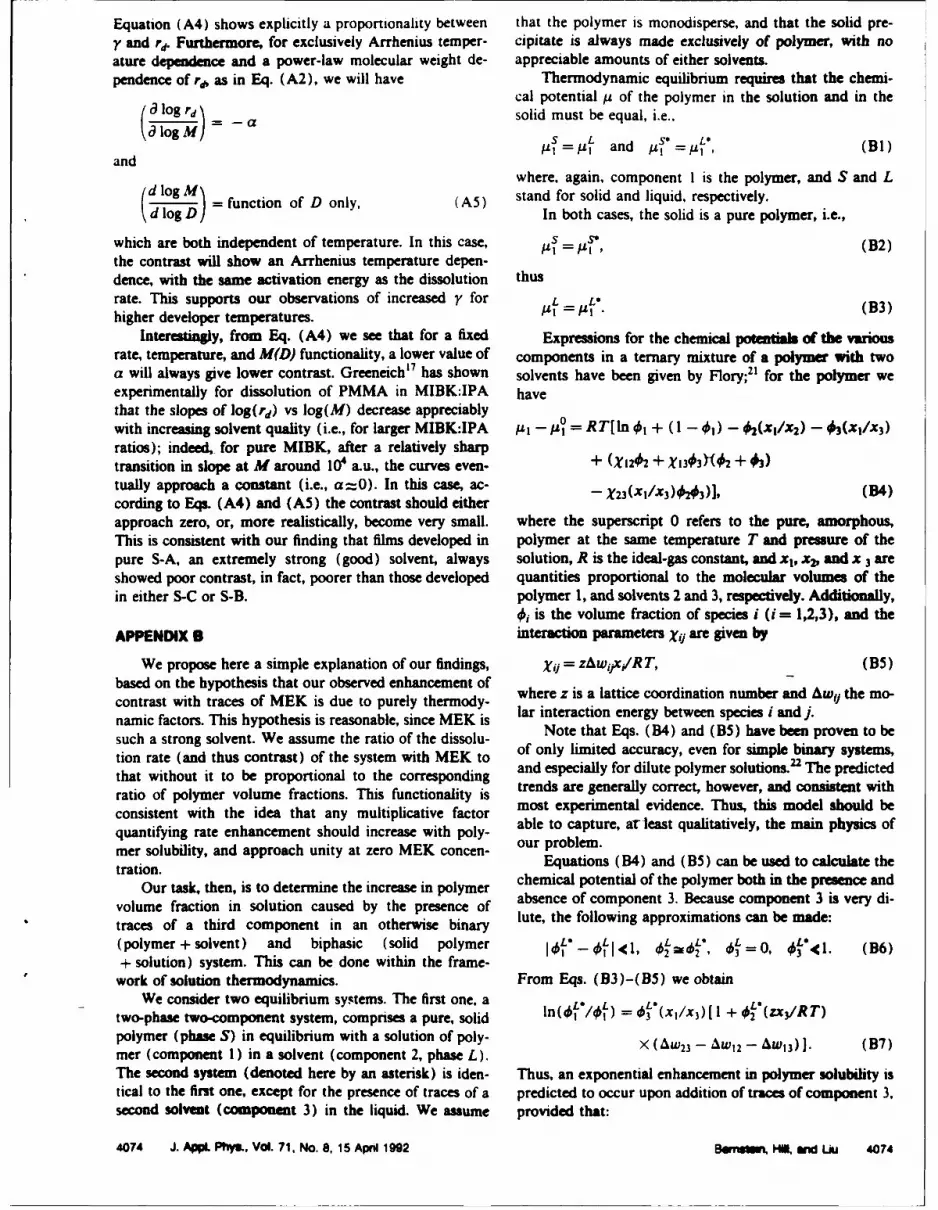
Equation (A4) shows explicitly a proportionality between that the polymer is monodisperse, and that the solid pre-y and rd. Furthermore, for exclusively Arrhenius temper- cipitate is always made exclusively of polymer, with noature dependence and a power-law molecular weight de- appreciable amounts of either solvents.pendence of rd, as in Eq. (A2), we will have Thermodynamic equilibrium requires that the chemi-
cal potential g of the polymer in the solution and in the
- -a solid must be equal, i.e..(C log M) }S L an (B
an 1 p n ,=A•, (B1)and
where, again, component 1 is the polymer, and S and Ld log M f stand for solid and liquid, respectively.
d -- fun( In both cases, the solid is a pure polymer, i.e.,
which are both independent of temperature. In this case, s 5= (B2)
the contrast will show an Arrhenius temperature depen-dence, with the same activation energy as the dissolution thus
rate. This supports our observations of increased y for L L' (B3)higher developer temperatures. k i (B3
Interesfingly, from Eq. (A4) we see that for a fixed Expressions for the chemical potentials of the variousrate, temperature, and M(D) functionality, a lower value of components in a ternary mixture of a polymer with twoa will always give lower contrast. Greeneich17 has shown solvents have been given by Flory;2" for the polymer weexperimentally for dissolution of PMMA in MIBK:IPA havethat the slopes of log(rd) vs log(M) decrease appreciablywith increasing solvent quality (i.e., for larger MIBK:IPA At -_0 = RT[In 0, + (1 - 0,) - 02(x,/x2 ) - •(Xi/X3)
ratios); indeed, for pure MIBK, after a relatively sharptransition in slope at M around 104 a.u., the curves even- + (XI202 + X1303Y(2 + #3)
tually approach a constant (i.e., a=0). In this case, ac- -- X23(Xl/X3)23)1, (B4)cording to Eqs. (A4) and (AM) the contrast should eitherapproach zero, or, more realistically, become very small. where the superscript 0 refers to the pure, amorphous,This is consistent with our finding that films developed in polymer at the same temperature T and pressure of thepure S-A, an extremely strong (good) solvent, always solution, R is the ideal-gas constant, and xt, x2, and x 3 areshowed poor contrast, in fact, poorer than those developed quantities proportional to the molecular volumes of thein either S-C or S-B. polymer 1, and solvents 2 and 3, respectively. Additionally,
0i is the volume fraction of species i (i 1,2,3), and theAPPENDIX B interaction parameters Xj, are given by
We propose here a simple explanation of our findings, xij = zAwijx'R T, (B5)based on the hypothesis that our observed enhancement ofcontrast with traces of MEK is due to purely thermody- where z is a lattice coordination number and Awy the mo-
namic factors. This hypothesis is reasonable, since MEK is lar interaction energy between species i and j.
such a strong solvent. We assume the ratio of the dissolu- Note that Eqs. (B4) and (BS) have been proven to be
tion rate (and thus contrast) of the system with MEK to of only limited accuracy, even for simple binary systems,
that without it to be proportional to the corresponding and especially for dilute polymer solutions.22 The predictedthat wthouttrends are generally correct, however, and consistent with
ratio of polymer volume fractions. This functionality is
consistent with the idea that any multiplicative factor most experimental evidence. Thus, this model should be
quantifying rate enhancement should increase with poly- able to capture, arleast qualitatively, the main physics ofour problem.
mer solubility, and approach unity at zero MEK concen- Euationd ala
tration. Equations (B4) and (B5) can be used to calculate the
Our task, then, is to determine the increase in polymer chemical potential of the polymer both in the presence and
volume fraction in solution caused by the presence of absence of component 3. Because component 3 is very di-
traces of a third component in an otherwise binary lute, the following approximations can be made:
(polymer + solvent) and biphasic (solid polymer 6L2"&L*, bL=o, *,. (B6)
+ solution) system. This can be done within the frame-
work of solution thermodynamics. From Eqs. (B3)-(B5) we obtainWe consider two equilibrium systems. The first one, a V( L L- L,
two-phase two-component system, comprises a pure, solid ln(0 1 101)=(b3 (X1 /X 3)[I + (zxVRT)
polymer (phase S) in equilibrium with a solution of poly- (Aw23 - "w12 - AW1 3)]. (B7)mer (component 1) in a solvent (component 2, phase L).The second system (denoted here by an asterisk) is iden- Thus, an exponential enhancement in polymer solubility istical to the first one, except for the presence of traces of a predicted to occur upon addition of traces of component 3,second solvent (component 3) in the liquid. We assume provided that:
4074 J. Appi. Phys., Vol. 71, No. 8, 15 Apri 1992 Bernstmn, wi- und Liu 4074
i136= [1 -,-b'(zx.,/RT)(A, - .- Aw 30J O the argument, the exponential can be approximated as a
(B8) straight line. From the temperature-normalized contrastdata we obtain fl(x 1/x 3) = 24. which is reasonable, in light
For13-, te ncrasecanbesubtanial snce(x 1 x1)is of our many approximations. and, possibly, some moreproportional to the ratio of the molecular weight of the fund anyappoimations i nhe to the mod a
polymer to that of component 3. Notice that an exponen-tial increase of the ratio (6L'/kt) with polymer molecular model itself. Again, it is worth noticing here that, given theweight does not necessarily imply an unbounded increase crudeness of our model, such "theoretical" results shouldof polymer volume fraction, since for higher, insoluble, be considered only for their qualitative value.molecular weights. the decay to zero of 6 will be faster A rate-enhancement curve, calculated from Eq. (B7)
than any concomitant growth of the enhancement factor. by assuming 63 = 0.02, ((x 1/x 0) = (M)/100, and an in-Flory, in his analysis of polymer fractionation by selective verse-square dependence of the dissolution rate on M, isprecipitation from binary mixtures, derived an equation given in Fig. 10 (Note that we have arbitrarily truncated[see Eq. (23) of Ref. 21] that is very similar to Eq. (B7). the enhanced-rate curve, since it would have shown an
In order to obtain the sign of 0 in Eq. (B8) it is nec- unrealistic upturn for higher molecular weights, due to ouressary to estimate the differences of the interaction energies assumption of a fixed inverse-square dependence of thebetween the various components. Following Gordon and original rate for all molecular weights. In reality, due to theTaylor23 (see also Ref. 18) in a semiempirical approach, finite solubility of higher fractions, the disolution ratewe assume the following proportionality [see Eq. (3)]: eventually drops to zero much faster than M- 2, and no
110,1 = A' (6p.-- )2 + ( 6 d, - 6 d,)2 + (64, - 6Ij) 2 ], upturn in the net rate occurs). Figure 10 should be corn-
(B9) pared with curves I and 3 in Fig. 5 of Ref. 17.
where i and j denote the particular substances, and 6p, 6d,and 6h are the polar, dispersive, and hydrogen-bondingcomponents of the solubility parameter, respectively. Inour case S'M. A. McCord and R. F. W. Pease, J. Vac. ScL TechwL B. 6, 293
(Aw 2 3-- Aw, 2 - AW 3 ) o (A2 3 - A2 - A1 3). (B1O) (1988).2D. C. Joy, Microelectron. Eng. 1, 103 (1983).
Hence, the sign of the interaction energy term on the left- 3w. J. Cooper, P. D. Krasicky, and F. Rodriguez, Polymer 26, 1069
hand side can be estimated from the properties of the pure (1985).
components. (Further theoretical refinements would re- W s.. aMoe and S. P. Beaumont. Solid State Technol. 23, 117 (1985).
quire that the factor of proportionality between Awi and 6B. K. DanieL,, P. Trefonas, and J. C. Woodbrey, Solid State Technol.A,. be a function of the molar volumes of the various com- 31, 105 (1988).ponents. Such refinements are not deemed necessary here, 'M. A. Mobsin and J. M. G. Cowie, Polymer 29, 2130 (1916).
where only rough estimates are of interest.) For a positive 1K. 0. Chiong, M. B. Rothwell, S. Wind, J. Nuochiun and F. J.
right-hand side in Eq. (13110), in Eq. (18) will also be Hohn, J. Vac. Sci. Technol. B 7, 1771 (1989).9V. K. Sharma, R. Pethrick, and S. Affrossman, Polymer 23, 1732
positive, indicating an enhancement of polymer solubility. (1982).
On the other hand, a negative term in Eq. (B10) may oJ. S. Papanu, D. W. Hess, D. S. Soane, and A. T. Bell J. Electrochem.
either signify an increase or a decrease of solubility, de- Soc. 136, 3077 (1989).pending on the relative magnitude of the various terms in 'A. N. Broers, J. M. E. Harper, and W. W. Molzen, Appi. Phys. Lett.
Eq. (B8). 33, 392 (1978).
It is interesting to estimate the sign and magnitude of S. P. Beaumont, P. G. Bower, T. Tamamura, and C. D. W. Wilkinson,Appl. Phys. Lett. 38, 436 (1981).
the quantity in Eq. (B130) for PMMA in MIBK with traces 3 H. G. Craighead, R. E. Howard, L. D. Jackel, and P. M. Mankiewich,
of MEK. This system should be reasonably close to the one Appl. Phys. Lett. 42. 38 (1983).we achieved experimentally. Using the pure-component 14 A. Muray and M. lsaacson. J. Vac. Sci. Technol. B 1, 1091 (1983).solubility parameters in Table II (MMA = 1, MIBK = 2, 5 All exposures were performed at the Center for Solid State Electronics
MEK =3), we obtain, in units of cal/mi, Research at Arizona State University.16W. J. Cooper, P. D. Krasicky, and F. Rodriguez, J. Appl. Polym. Sci.
A2= 14.49, A2= 11.57, A• 3 -2, 31, 65 (1986).17j. S. Greeneich, J. Electrochem. Soc. Solid State Sci. Technol. 122, 970
giving (1975).g8 C. A. Kumins and T. K. Kwei. in Diffusion in Polymers, edited by J.
A23 - A-, - %'3 = 0.92 cal/ml. Crank and G. S. Park (Academic, New York. 1968), p. 107."Q IF. Rodriguez, Principles of Polymer Systems, 3rd ed. (Hemisphere, NewWe see that the overall interaction energy is positive, so York, 1989), p. 36.that we would indeed expect an enhancement of solubility 2°E. Gipstein, A. C. Ouano, D. E. Johnson. and 0. U. Need III, Polymer
in our case. consistent with observations. Eng. Sci. 17, 396 (1977).2' P. J. Flory, Principles of Polymer Chemistry (Cornell University Press.Furthermore, it is possible to extract from our data Ihc.N ,35) .59FurhemoeitIthaca, NY, 1953), p. 549.
with Eq. (B7) an "experimental" value of P(x 1/x 3). The 22P. J. Flory, Principles of Polymer Chemistry (Cornell University Press,
linear increase of contrast with percent MEK in Fig. 7 is, Ithaca, NY, 1953). p. 559.in fact, consistent with Eq. (B7), since for small values of 23J. Gordon and J. S. Taylor, J. Appl. Chem. 2, 493 (1952).
4075 J. AppI. Pti.. Vol. 71, No. 8. 15 April 1992 Bernsten, Hill, and Liu 4075

Fabrication of ultrasmall tunnel junctions by electron-beam lithographyS. J. Koester,") G. Bazan, G. H. Bernstein, and W. PorodDepartment of Electrical Engineenng. Universitv of Notre Dame. Notre Dame, Indiana 46556
(Received 3 October 1991: accepted for publication 5 November 1991 )
Fabrication of a variety of ultrasmall tunneling structures is presented for possibleapplications in single electronics. Two main structures are described: (i) arrays of nanometer-scale metal dots and (ii) single and multiple linear tunnel junctions formed by overlappinglines. Very large, uniform particle arrays were fabricated by electron-beamlithography (EBL) with particle diameters as small as 25 nm. The advantage of our dotarray system is its high degree of uniformity and very small junction size coupled with the useof isolated particles to reduce stray capacitance effects. Single and multiple linear tunneljunctions were fabricated by EBL using single-layer resist and angled evaporations. Ourfabrication technique differs from previous ones in its ability to create very small tunneljunctions without the need for multilayer resist systems or precise knowledge of the angle ofevaporation.
I. INTRODUCTION effects wash out remains near liquid-helium temperatures.The other technique, pioneered by Dolan,9-10 is the use of
The semiclassical theory of single-electron tunneling electron-beam lithography and angled evaporations to cre-(SET) has proven to be useful in describing the behavior of ate narrow, overlapping metal lines separated by thin tun-tunnel junctions with ultrasmall capacitances.' In this the- nel barriers. This technique has proven successful at creat-ory, the Coulomb effects due to the individual electrons ing junctions as small as 30 x 30 nm2 .2 However, even verybecome increasingly evident as the single-electron charging small junctions produced this way can produce large ca-energy of a structure with capacitance C surpasses the en- pacitances if the leads connecting the junction significantlyergy of thermal fluctuations at temperature T, i.e., couple to their environment or to each other.
e2 /2C > kT. (1) The purpose of this work is to investigate improved
designs and fabrication techniques which can further en-Here, e and k are the electron charge and Boltzmann con- hance the performance of single-electron tunneling struc-stant, respectively. According to (1), the observation of tures. This paper focuses only on fabrication issues, whileindividual electrons requires cryogenic temperatures, even the electrical characterization of these tunneling junctionsfor the smallest tunnel junctions reported. 2 This issue has will be reserved for future publications. In Sec. II, we de-become increasingly important for the future of new de- scribe the first of two experimental structures, arrays ofvices which might utilize single-electron charging ultrasmall metallic dots, along with the fabrication proce-effects.'- Such devices might operate at temperatures dure and fabrication results. In Sec. III, we discuss similarabove 4.2 K if the characteristic capacitance of a junction issues for systems of linear tunnel junctions formed bycan be reduced below 10- 16 F while maintaining narrow overlapping metal lines. Finally, we discuss in Sec. IVtunnel barriers. Therefore, a major issue facing the growing some of the pertinent issues involved in creating suchfield of "single electronics" today is the ability to fabricate structures, as well as the advantages and disadvantages ofsmall, reliable capacitor structures for operation at higher our approach over those previously reported in the litera-temperatures. ture.
The most common type of system used in studyingSET effects is the metal-insulator-metal tunnel junction 11. ARRAYS OF ULTRASMALL METAL DOTSstructure. With this type of system, researchers have uti-lized two basic approaches to achieving capacitances small The first structure discussed here is composed of aenough to experimentally observe single-electron charging. large array of very small metal "dots" sandwiched betweenThe first technique is to use natural particle arrays as the two electrodes and separated by thin tunnel barriers. Acenter electrode of a double-tunnel junction structure.'- It schematic of these dot arrays is shown in Fig. 1. Our struc-is well documented that the particle islands formed by ture is different from previous ones utilizing isolated par-evaporating metal onto an insulator such as A120 3 can ticles because the particle array is fabricated by direct ex-have effective capacitances as low as 5 X 10- "8 F. 8 Since posure of high-resolution electron-beam lithography. Thethe particles are isolated they do not suffer from stray ca- advantage of using EBL to create the particle array is thatpacitance effects. However, because the particles have it can produce uniform dots of equal size and spacing,widely varying sizes, the temperature at which the SET while still providing very high resolution.
The fabrication procedure for our structures is as fol-
"Proumt addres: Dqeartmat of Electrcal Enpnaertng, Univerity of lows. The base-electrode metal is evaporated onto a Si sub-Cajiforaa at Santa Barbara. Santa Barbara. CA 93106. strate through a mechanical shadow mask forming a 10-
1918 Rev. S&. khum 63 (3). Mmdr liM 00344741/92/03•I1g-.04).OO CD IM A1nwkin Inetftut of Phyics 1916

tunnel barneroot arrayGe insulailontunnel barneroaso-eoeclrode
S, substrate
FIG. 1. Cross-sectional diagram of a single-electron tunneling structureutiling a lithographically fabricated particle array.
mil-wide line. Typically, this metal is Al and the barrier,always an oxide in our case, is formed by exposure to air FIG. 2. SEM micrograph of a gold dot array with a 100-m pitch and
during the subsequent processing steps. Next, an insulation 25-30-nm dot diameter.
region is patterned by standard EBL and lift-off to reducethe effective junction area of the structure. This is accom- was used to provide higher contrast in the SEM micro-plished by creating a 500X600-#um" rectangular germa- graphs). It was found that dot diameters as low as 25 nmnium region with a 20X20-,m2 "hole" in the middle, could be achieved fairly routinely with extremely success-which covers the base electrode except for the small central ful lift-off results. Even with a dot spacing of 100 rnm,
area. Next, a 24 x 24-14m 2 dot array is aligned and exposed nearly 100% lift-off could be achieved. There are severalby EBL to the previous pattern in such a way that the reasons for the high quality of the lift-off. Firstly, the use ofarray entirely fills the opening in the Ge insulation. Once a relatively high accelerating voltage (50 kV) reducedagain this pattern is evaporated and lifted off, typically proximity effects, thereby creating a more uniform arrayusing 300 A of Al. The second oxide is formed as before, by and forming sharper features in the resist. Next, adding aexposure to air during the subsequent processing. Finally, small amount of MEK to the usual MIBK developer hasa gold counterelectrode is patterned over the active area by been shown to enhance the contrast of the developer andEBL and lift-off as before. The Ge insulation" separates improve lift-off characteristics.14 Finally, the appropriatethe base electrode and counterelectrode in all places except choice of PMMA layer thickness (up to 2500 A) helped tofor the 20 X 20-pm 2 junction region, thus minimizing leak- improve the aspect ratio of the resist pattern, making it
age and shunt currents. more suitable for lift-off than thinner resists.In order for such a system to display single-electron
effects at T > 4.2 K, the dots must have diameters less than Ill. LINEAR TUNNEL JUNCTIONS35 nm, assuming hemispherical dots and a temperaturethreshold of T = e2 /4kC.' 2 In addition, the dots should The other types of structures investigated are single-
be spaced as closely together as possible to limit the par- and multiple-junction systems created by overlapping thin
allel shunt current which can flow by directly tunneling metal lines. Excluding contact pads, these can be created in
from one electrode to the other. This is equivalent to im- a single EBL exposure and two successive angled evapora-
proving the signal-to-noise ratio of the SET effects. Thedots must also be very uniform in size and spacing over theentire array. Although it has been predicted12 that a Cou-lomb staircase can persist in a system with a standard de-viation in particle capacitance as high as 25%, muchsharper steps are predicted if the capacitances of the par-ticles are equal.
Therefore, to meet these requirements we have fabri-cated our arrays using the following parameters. A high-resolution EBL system' 3 was utilized for all exposures. Thedots were exposed at 50 kV, in 1400-2500 A of poly(me-thyl methacrylate) (PMMA) in square arrays with 100-250-nm spacing, and developed in a 99.7% 1:3 methylisobutyl ketone (MIBK)/2-propanol, 0.3% methyl ethylketone (MEK) solution for 15 s. Typically, the exposuretime was limited to about 10 min in order to minimize theeffects of current drift and loss of focus.
Figures 2 and 3 show SEM micrographa of typical dot FIG. 3. Medium magnification view of a 250-nm-pitch gold dot array
arrays fabricated by the above technique (except that gold showing 100% lift-off in this ares.
1919 POV. SOL WuWRm, VOL 03, H& 3, March 1i9 Tunnel luncuons i191

FIG. 4 SEM micrograph of an AI/AIO,/AI tunnel juniaton with an areaF Ibout 304 mco nm-A. " FIG. 6. SEM micrograph of a series of linear tunnel junctions. The barrepresents I 14m.
tions with an intermediate oxidation step. The motivationfor this particular structure is to create small junctions However, this can be corrected by allowing a certain over-
utilizing a simple and straightforward fabncation tech- lap of the crossing resist lines and shifting the pattern po-nique. sition. It is not sufficient to merely make the actual junc-
An example of a very small single-tunnel junction is tions small, because stray capacitances due to the centralshown in Fig. 4. This pattern simply realizes a junction bar may still be significant. The most important require-formed at the intersection of two long, narrow lines. It was ment of this type of structure, therefore, is that the centralcreated by first exposing a crossed pattern in 2500 A, of electrode be as small as possible.PMMA. and developing as discussed above. Next, two an- The above processing technique has proven to be very
gled evaporations of 300 A of Al were performed with a reliable. Figure 6 shows a set of multiple-tunnel junctionsbrief (5-min) oxidation step in air between them. The demonstrating the feasibility of fabricating large-area
evaporations were carried out at such an angle (approxi- structures.mately 450) that only one line would be metallized at atim-. As shown in Fig. 4, the two successive angled evap-orations resulted in a tunnel junction with an area of 30 IV. DISCUSSION
,60 nmT.This same technique was used to create multiple-tun- The structures which utilize Iithographically fabricated
nel junctions in series. An example of a double-tunnel junc- dot arrays, as described in Sec. II, merge the precision and
tion is shown in Fig. 5. Here. two parallel lines overlap a high resolution of EBL with the use of isolated particles.
,mall. isolated crossbar which acts as the centrai electrode. thereby offering clear advantages for the study of SET ef-
When the resist shadows the incoming evaporant. the fects. Particle arrays of this type should result in the small-
metal lines are not exact replicas of the resist features. est capacitance attainable in a structure fabricated by con-ventionally employed lithographic techniques. Anadvantage of dots used in this system is that no leads arerequired and the use-of dense parallel arrays might alsolead to temporal and spatial correlation effects with noveldevice applications.
To determine the value of capacitance for very smallisolated particles fabricated by EBL, the dot can be mod-eled using a concentric sphere approximation. For a dot ofradius r and dielectric thickness d, the capacitance is givenby
C = 4 riExrr [ I -- (rd). (2)
For the smallest dot size achievable by EBL usingPMMA. say, r = 5 nm. and typical parameters of d = 2nm and c, = 8. the corresponding minimum capacitance isCm,, = 1.6 x 10 - 1" F. Conceivably, one might achieveeven smaller capacitances by the use of novel lithographic
FIG 5 SEM micrograph of a system containing two linear tunnel juinc- techniques such as those utilizing the scanning tunnelingtorns in series. microscope. 1e
1920 Rev. SeL Inetrum., Vol. 63. No. 3. March 1992 Tunnel functions 1920

The properties of the thin tunnel barriers are of major varying oxidation properties, the thickness of the barriersimportance to the behavior of SET structures such as those can, in principle, be controlled by appropriate metal selec-which are biaed on isolated particle arrays. As stated be- tion.fore, the formation of the tunnel barriers was normally Our approach to the fabrication of linear junctions of-accomplished by utilizing the natural oxidation properties fers distinct advantages. Firstly, our fabrication techniqueof aluminum to form a thin layer of oxide. However, we does not require a multilayer resist system. Secondly, byfound that the oxidation of the base electrode was difficult using perpendicular crossing lines for each junction, noto control because the sample had to be repeatedly exposed residual patterns are created from the two evaporations,to both air and elevated temperatures ( 170 "C for PMMA thereby avoiding the presence of unnecessary stray capac-baking) during processing. The result was that all junc- itances. Another feature is that the sizes of the junctions dotions with natural A120 3 barriers were very resistive, thus not depend upon the angle of evaporation, but only on theprecluding the observation of SET effects. width of the developed lines. In fact, the angle of evapora-
An alternative way to control thickness of the tunnel tion does not need to be known precisely becuue the cross-barriers is to form the insulator through deposition rather ing limes can overlap slightly without greaty reamug thethan oxidation. This can be achieved, for example, by sput- total capacitance of the system. These features make thister deposition or reactive evaporation of 15-20 A of technique easy to implement while maintaining the caps-A120 3 onto a nonoxidizing metallic substrate. The advan- bility of producing junctions with dimensions at the limitstap of these techniques is that the barrier thickness can be of electron-beam lithography.precisely controlled and does not change during subse-quent processing. Another advantage of using deposited ACKNOWLEDGMENTSbarriers is that the space between the dots is filled with The authors are indebted to S. T. Ruggiero and N. M.both barrier materials rather than that of the base elec- Jiawi for useful conversations. This work was supportedtrode. This can greatly reduce the parulel shunt current In part by the Offie of Naval Researc and 1BhMwhich might low between the dots,' especially since theresistance of a tunnel barrier increases exponentially with 'IL. K. Likhaam. IBM J. Rea 03ev. 32, 144 (1963).thickness. However, in the event of damage to the oxide 2T. A. Pltm and 0. J. Doela, Phys. Rev. Ltt. 5f, 109 (1917).
during processing, a short circuit between electrodes could 3M. Amman, K. Muilen, and -. Ben-Jacob, J. Appl Phys. 4a, 339(1988).result. This is less of a problem with natural b s K. K. Lham, IE Tram. Mato. 23 1142 (1987).
which, when exposed to air, tend to "heal" by themselves 'L J. Geerliss, V. F. Anderegg, P. A. M. Hoieg. J. F. Mooii H.if damaged. Podhier, D. Esteve, C. Ueba and M. H. Devou. Phys. Rev. LeUm 6K,
A final issue for dot arrays fabricated by EBL is the 2691 (1990).'H.It. Zellar and 1. Giaeve, Phi.Rev. 181, 79 (199).choice ofLdot metal. For artificial barriers, metals with &-S. Kzmin and K. K. Lkuev, JETP M Lt 44951 "7•M).
small grai sizes, such as gold alloys, provide optimum 1J. B, Dam and S. T. Rugpero Phby Rey. Lat., A807 (I1 ).conditions for uniform coating and lift-off. When natural '0. 3. Dolan, APL. Phy. Lem 31, 337 (1977).barriers are used, the choice of metal determines the prop- 200. J. Dolan and T. A. Fulton. IEEE Electron. Dev. Let 4,178 (1983).
" E. L. Hu, L D. Jackel, and R. E. Howard, UEE Tranm. Electron.erties of the oxide. If the base electrode barrier is thick, Device, ED-8, 1312 (1981).then it is desirable to make the dot barrier thin, and vice 12K. Mullen, E. Ben-Jacob, R. C. Jaklevic, and 7.. Schum, Phys. Rev. Bversa, so that the resistances of the two barriers are very 37.98 (1988).different. This has been shown to sharpen the steps of the "3 G. Bazin, J. Monteiro, and G. H. Bernstein (unpubildhed).
he.3 'e se G. H. Bernstein and D. A. Hill (unpublished).Coulomb staircase in the l-Vcurve. 3 Metals which we have "D. Joy, Micreect. Eng&. 1103 (1983).lifted off include Al, Sn, and Pb. Since these metals have '6D. M. Eigler and E. K. Schweizer, Nature 344, 524 (1990).
1t11 Rev. Sea bim, VoL 63, No. 3, Marh 192 Tunnel MoIes 1921
Superlattices and Microstructures, Vol 11, No. 2. 1992 189
FIELD EFFECTS IN SELF-CONSISTENT TRANSPORT CALCULATIONSFOR NARROW SPLIT-GATE STRUCT7URES*
Henry K. Harbury, Wolfgang Porod, and Caig S. LomDepartment of Electrical Engineering
University of Notre DameNotre Dame, IN 46556
(Received 19 May 1991
We study local potential variations due to self-consistent space-charge effects in cal-culation of coherent transport in narrow split-gae sum We prem a numericaltechnique based on calculating the Harree potential from the charge density obtained bysolving the two-dimensional effective-mass Schrodinger equation for scattering states,and from the bound charge density obtained from a semi-classical Thomas-Fermi screen-ing model. This method allows us to obtain the local self-consistent potential variationsclose to scattering centers exposed to an incident flux of electrons.
1. Introduction ference between iterations converges to within a desiredtolerance.
Many recent studies have appeared in the literaturewhich present calculations of conductances in narrow split- A. Problem Domaingate structures that can be realized using advanced fabrica-tion techniques I1l. In these calculations the Schrddinger Our model of the device geometry consists of a dis-equation is solved for the channel geometry to obtain trans- cretized calculation domain, Q., of mesh elements con-mission coefficients, from which the conductance is ob- nected to input and output leads. Q, and 02, as shown intamed. It has been pointed out 12] that self-consistent ef- Fig. 1. The current carrying leads attach to the edges offects may be significant in these structures, but it has been the calculation domain, at .r = 0 and .r = 1, and extendprohibitively difficult to include them in the numerical cal- to infinity. Although the leads are not part of the calcu-culations. lation domain, the charge contained in the leads must be
We present a technique for capturing self-consistent included in the numerical model for the Harree poinntiat.space-charge effects in two-dimensional transport calcula- For simplicity, we assume hard-wall boundary conditimstions in split-gate structures. We study the self-consistent for the conducting channel. A split-gate structue is real-variations in carrier density and local potentials close to ized by adding a large fixed potential in the gate regionsscattering centers exposed to an incident flux of electrons, of the problem. The size of the calculation domain must
be sufficiently large that the disturbance due to the con-2. Numerical Method striction has decayed at .r = 0 and .r = I. Selecting device
Self-consistent electronic states are obtained through geometries that are symmetric across the channel enablesus to solve the proolem on only one half of the originalan vdomain. The resulting bandwidth reduction significanony
ing current carrying boundary conditions. Any bound lowers the computation time.electronic charge is approximated by the semi-classicalThomas-Fermi screening model. The Hartme potential due B. Effective Mass Schr6dinger Equationto the electron density is explicitly determined from thetotal charge density in each iteratin, and is used to calcu- The 2-D effective-mass Schrodinger equation is repeat-late the electronic states in the subsequent iteration. The edly solved on the discretized spatial domain for the trav-self-consistent solution is obtained when the potential dif- cling wave "scattering states". V, denotes the confining
07494-036/92/020189 + 056 02.00/0 © 1992 Academic Prm Limited

190 Suparlattices and Microstructures, Vol. 11. NO. .' M
y =-d ' DTie sum includes the wave-functions due to injection firomboth lead I and lead 2. In the linear response regime.
injection is symmetric for both leads and this can be usedto reduce computation time. We.typically find that iwww
FLA 11 terms in the summation over electronic states ar suffichas.Bound electronic stares can exist inside the
ing region if the total poential dips below its asymp•value far into the leads. The quantum mechanical ekxe,
y--O Mo tn density obtained for traveling states does not coammany contribution that may arise from bound charge inside
=x~l the problem domain, Qt,. If this contribution is neglecad
the electron density would be underestimated in the re-FIGURE 1. Schematic of the channel geometry showing gion of a potential well, resulting in a larger at-racthe finite element domain, 00, and the leads, Q, and %. Hartn•e potential and subsequendy an unstable nd my-The shaded regions represent the confining gate potentials. dondition. As a first order approximaton, we choomli
model the bound-state electroic charge density with- thsemi-classical Thomas-Fermi screening model. If the po-
channel potential. V11 represents the self-consistent Hantree tential in the solution domain is lower than its asymptoticpotential, and ,n is the electron effective-mass, value in the leads, t',(i..) < V(0.t). then a semi-
J- classical electron density is obtained at the point (z, y) by
-,--"V~ + l•--(.r. ,j) + V,1 (r, I.(ry) = E z.!). TF(7. !) = -- t,•(0. ,y) -- W,'(x-Y)I, where Vt, is thetotal potential used in solving the Schrodinger eqa
.() This simple approximation over-estimates the total elec-I:cep inside the leads, i.e. far from the scattering region. rndniyi h eino oeta elhc•wregon. tron density in the region of a potential well becoms we
we assume free electron propagation. The electronic wave fill a discrete quantum system with a continuous eberm -function can be factorized into a longiudinal plane-wave density. The over-estimation, however, will cause the po-pan, t.rp( 1'kx), and a transverse part with quantized modes, tential well to become moe "shallow" in the subseqen\,,,(!/), which are due to the confining potential of the iteration resulting in a smaller semi-classical electror-den,channel. The scattering eigenstates for injection from theleft-hand lead, Q,, in mode m are, therefore, of the form, To maintain chap neutaity, a compensating podYt --
background charge, ps, is needed. The backgiouritici
= { ) z---o isobtainedbyenforcingchargeneutralityin theead, 'Th"z. •, ,1,e?'* (!) r -- +local disturbance caused by any constricton is assur'e& "
(2) be completely contained within the problem domraia 0"with negligible effect in the leads. This criteriorraffAs'The index n runs over all possible tranisverse modes ustmoethcareenv'iteinnilyeis t"
with E = E. + (h '•k,/2m'), which includes both traveling l as aonuo the charge dens ity at the ely e5Iand evanescent states. leads as a continuation of the cha, density at the edgeWk-
e the problem domain. pa = fJ p,,(Oy)dy = fo• P, (,. 3Tle. efiniz e lementod is used t reduce the prob-erm to.a lisp system of coupled linen equation& . The Tis model for tie pouhr bacground
fact that in most 20EG systemss thee ppositiveJQuantum Transmitting Boundary Method [31 is used to fc hti ot2E'ytm h oiied
in a parallel plane isolated from the carriers by a VpWl& 'implement the finite clement boundary conditions appro- lyr lhuhw oncmdltesae a•-T a*layer. Although we do not model the space layeIr-d"Ppriate for the current carrying leads.calculations, one could, in principle, use an "efreedW
C. Charge Density positive background charge density without changing doealgorithm 141.
The elkmon density in the channel due to current car-rying states is obtained by explicitly summing over the D. Hartree Potentialcontributions of all occupied scattering states. We assume The Hart potial at any locatio (r. y) is othe linear response regime and zero temperature. The scat-tering stare electron density is then given by summing over channel,
channel, 'all states with E <5 EF,..•3 ••:
IiQAI(T, t) = E IV'dz,Y)12. (3) 4,(:y re 721 --' ss1 . -0" + p') -dr' dur•,'
Reproduced From .
Best Available Copy

Superlattices and Microstructures, Vol. 11, No. 2. 1992 191
The integral can be broken into three distinct contributions. E. Self-ConsistencyI. 1, = I i t + I, + INS. corresponding to the domain, Q,),and the two leads, Q, and Q,, respectively. The tmrm due The resulting Hartree potential is used to modify the
to the charge density inside the solution domain, Vi1., is total potential on which the Schrodinger equation is solved
explicitly calculated by Gaussian quadrature on the finite in the subsequent iteration. The self-consistent potential
elements. The components of the Harune potential due and charge density am obtained when the difference in
to the infinite leads, V"•' and Vn, must be, in part. cal- the total potential between iterations converges to within a
culated analytically. Using the conditions of charge neu- specified tolerance.
trality across the leads, f,' p(i. y) = 0. and of translational
invariance down the leads, pi.r > 1. y) = p(l. y), yields 3. Results
r = () A. Open Channel
irr We first investigate the electronic charge density aind
The above integral across the lead is evaluated numerically the Hartree potential for an open. unconsmcted channeLfrom the charge density at the edge of the finite element The solutions must show translational invariance down diedomain. /pi1. ,/. We obtain a similar Hartree term due to channel, namely plz.y/) = p(y) and V,,(z., 1 ) = VN(y).the charge density in the left lead, V11'. This provides a test for the Hartree potential obtained by
summing U"', iN, and %W,'. We choose to study single
mode injection by occupying states up to a Fermi energy
that is below the second subband in the leads. Fig. 2shows in part (a) the Harree potential due to the solution
domain V,1* and in part (b) the sum of both lead contribu-
tions, I "" + t", after the first iteration. The total Hartee2 potential, which is the sum of (a) and (b), results in the
potential shown in Fig. 2(c) and exhibits the desired trans-
a
bb
!,L 1 0"
10"1
C 10-'
0 0 s 20 25 *0 31 00
Iteration NumberFIGURE 2. The components of the Hamee potential forthe openchaml after the firstinmrtoni: (a) 1, "4.(b) V,,"+ FIGURE 3. Shown is (a) the converged open charmel
S•,(c) V .. po u re di and (b) the istristi ento .

192 Superlattices and Microstructure~s, Vol. 11. No. 2, 1992.
FIGURE 4. Shown is (a) the charge density for the con-stricted channel (WNW structure) after the first iteration,(b) the new total potentiai after the first iteration. (c) theseii-classica electron density in the second iteration, and(d) the total charge density after the second iteration.
lational invariance. This clearly shows that the Hartree po- Fig. 4(a) the charge density after the first ito fortential due to charge in the leads exactly compensates for single mode injection, and in Fig. 4(b), (c) and (d) thethe potential due to charge within the domain, and is a very new total potential used in the second iteration, the semi-critical test of our numerical method. Because the total po- classical electron density, and the total charge density aftetential in the solution domain, Q0, does not drop below its the second iteration respectively.asympeotic value in the leads, thene ame no bound elec- The first iteration charge density far from die auintronic s1ASs in the open channel. T"he Hartre potential in tion asymptotically approaches the case of an undi-s1u1 1Fig. 2(c), obtained from the completely quantum mechan- system. The leakage of charge between die spitk pas inical electron density, is used to modify the total potential the first iteration is small enough that the chug dendiy iswith which the Schrfdinger equation is solved on the sub- Fig. 4(a) resembles the solution of the totally cuistileedsequent iteration. Fig. 3(a) shows the converged solution channel [5]. Thie smaller electon density in the$ Mae-after 37 iterations, and Fig. 3(b) plots the change inthie gion in Fig. 4(a) results in dhe ftumodnfof apou=Wiatotal potential between iterations versus iteration number. well through the Hartree aem. used lo obtain doe SOta pD-T'he algorithmw is stable and convergent for the open chan- tential shown in Fig. 4(b). This poloal welf into Snel and. as Fig. 3(a) indicates, the "floor" of the quantum region will, in subsequent iterations, cwms m~sw inwire is "buckld's by several meY. the local electro density near the -ca-eing re Itu ThisB. Constrictod Chbannel results both from an increase in occupied traveling sums
throught the gam mpon and from the scmi-claz~aicLiinWml~ttit gaa puitiay consticted channel, for the bound electmo denst~y Ahwn inft:. 41"
our model for a narrow spkbnga Am. ~so im. since the potential in the g region dips be~low dM -

Superlattices and Microstructures, Vol. 11, No. 2, 1992 1 93
tential far into the leads. The total charge density obtained allows us to investigate the local self-consistent potentialin the second iteration, due to both the electron density .arnations close to scattering centers exposed to an incidentof the traveling states and the semiclassical bound elec- flux of electrons.tron density, is shown in Fig. 4(d). The increase in the For the case of an open channel, or quantum wire, weelectron density near the scattenng center is clearly visi- have demonstrated the validity of our method and achievedble. Although not fully converged, it is clear from these a fully convergent solution. We presented some results forcalculations that the oscillations in the local field near the a partially constricted channel, or narrow split-gaze smiuc-scattering center due to self-consistent space charge effects ture, but for this case convergence has been difficult tocould be significant in transport calculations since they will achieve. Mor work is needed to ensure convergence ofeffect the transmission amplitudes of the structure. The os- the self-consistent cycle for general split-gate structures.cllations in the potential due to a scattenng center in the7(X) channel can extend up to a half micron into the leads, 5. Referencesand are on the order of a few meV. Although the poten-tial well in the scattering region does not become deeper 1ll Nnno.xtruictiren. Phystex and Fabrication. eds. M.in later iterations, we have found it difficult to achieve A. Reed and W. P. Kirk, (Academic Press, 1989).convergence for split-gate structures. We are currently in- f21 L. Escapa and N. Garcia. Appl. Phys. Lett. 56,vestigating various convergence schemes and more work 901 (1990).is needed on this problem. (31 C. S. Lent and D. J. Kirkner, J. .ppl. Phys. 67,
4. Conclusion 6353 (1990).[4) J. A. Nixon and J. H. Davies, Phys. Rrr. B 41,
We have presented a method which incorporates self- 7929 (1990).consistent space charge effects in transport calculations for [51 H. K. Harbury, W. Porod, C. S. Lent, Proceed-narrow split-gate structures. Our method uses an iterative ing., of the Seventh International Conf'erence onsolution of the effective-mass Schrodinger equation. with the .Numerical AnalysLi of Semiconductor Devicesa semi-classical model for bound electronic charge, and and !ntlgrtrd Circuits. N.4SECODE-7, p. 136,explicit calculation of the Harree potential. This method ed. by J. J. H. Miller, (Front Range Press, 1991).
Superlattices and Microstructures 'o/ I 7 vo 2. 1992 237
ON THE ATr'AINNIENT 01 OPTIMLM DEVELOPER PARAMETERS FOR PMMA RESIST
Gary H Bernstein' and Davide A. Hill'
"Department of Electrical Engineering'Department of Chemical Engineering
University of Notre DameNotre Dame. IN 46556
,Received 19 May 1991)
Because of the uniquely high resolution offered by poly(methylmethacrylate) (PMMA) for practically all forms of lithography, its technologicalsignificance remains strong. We have found significantly higher contrastdevelopers for PMMA which have shown improved resolution, less susceptibilityto proximity effects and better lift-off properties with no loss of sensitivity toexposure. We report data which demonstrate an improvement in contrast bymore than 35% with the addition of as little as 1.3% methyl ethyl ketone (mek)to other common developers. We discuss a model which explains the observedcontrast enhancement and predicts that for small changes, an increase in eithermek concentration. temperature or develop time increases contrast. We includeexperimental evidence in support of temperature and mek related improvements.
I. Introduction such properties as lift-off reliability, proximity effectimmunity and. to some extent, resolution, are all
Of all matenals utilized in the fabrication of improved.nanostructures, poly (methyl methacrylate) (PMMA) We have found that several parameters canis among the most important. PMMA remains so increase the contrast of PMMA. First, we found thatpopular as a positive resist that virtually all laterally adding a very small percentage of methyl ethyl ketonedefined quantum devices rely on PMMA for patterns (mek) to other common, aevelopers effects a drasticbelow 100 nm regardless of the lithographic technique improvement in contrast, dimensional consistency andemployed. In fact, PMMA is the only proven positive lift-off quality. Serond, we hive found that, over aresist usable into the 10 nm regime. (Contamination narrow temperature range, an iacrease in temperatureresist is utilized for etch masks in this dimensional also improves ccntrast. Finally, as discussed inregime, but is slower and more difficult to work further sections. we propose that an increase inwith.) develop time is also predicted to improve contrast.
The typical manner in which PMMA isemployed is that of exposure to electrons, X-rays ordeep UV light followed by development, metallization 2. Experimentaland lift-off. The resolution of the resulting metalpattern depends on both the width of the defined line Contrast results for a variety of developerand the quality of the edge profile in the resist. In formulations were determined using a standardturn, edge profile depends on the contrast. y'. of the technique': 2 1. Using electron beam lithography (EBL)resist/developer system. Contrast is defined as the at 40 kVM we exposed 25 50 pm x 50 tum squares inmaximum slope of the curve of normalized resist 950,000 amu PMMA. 0.4 to I tAm thick with a seriesthickness remaining after development as a function of of doses, developed for various times andthe log of the exposure dose. As contrast increases, temperatures. and determined the normalized resist
0749-6036/92/020237 --04 $02.00/0 © 1992 Academic Press Limited

238 Superlattices and Microstructures. Vol. 11, No 2. 1992
thicknesses by surface profilometry using a Sloan The primary ingredients of the developerDektak 11 profilometer. The quality of the data was mixtures were chosen from solutions commonlyexcellent, and an example of the raw data is given in employed as developers for PMMA. These areFig. 1. Variations in resist thickness were shown to methyl ethyl ketone ('mek"):ethyl alcohol (EtOH)have no effect on the results. Experimental par- 26.5:73.5 (mixture referred to here as "MEK").ameters and contrasts are summarized in Table 1. methyl isobutyl ketone (mibk):isopropyl alcohol (IPA)
1:3 (mixture referred to here as "MIBK'). and 2-ethoxy ethanol (Cellosolve or "cs");methanol (MeOH)
__................. (mixture referred to here as "CS"). These mixtureswere chosen in their complete forms due to their
08 known properties as developers of PMMA. It shouldbe noted that solubility properties of mixtures of
I- 06 •several solvents are extremely difficult or impossibleto predict, and such an exercise will not be attempted
0here. In subsequent sections we offer a qualitativeS0 4 • 2 1 20 1 ,s wmo ;'
explanation of the role of the harshest component.S... , ,san",o,, mek, in improving contrast and offer guidelinesE02 0 toward future improvements in contrast.z :"
0 4".-. 3. Results and Discussion
Dose (Coul/cm') For mixtures given in Table i, we measuredcontrast and plotted the results as a function of inverse
Figure 1: Example of data from which contrast is temperature as shown in Fig. 2. A trend ofcalculated. increasing contrast with temperature in the range
Table I: Summary of contrast experiment data.
Sample volume volume volume Develop TempI.D. percent percent percent time
MIBK CS MEK (sec) '
1 0 100 0 5 19 5.7
2 0 100 0 5 21 7.0
3 100 0 0 45 19 7.0
4 100 0 0 45 21 9.3
5 66.4 32.0 1.6 10 7.7
6 66.4 32.0 1.6 10 7.0
7 49.6 48.0 2.4 10 8.2
8 49.6 48.0 2.4 10 8.5
9 50.1 45.4 4.5 10 18 7.9
10 50.1 45.4 4.5 10 18 7.9
11 50.1 45.4 4.5 10 19 9.4
12 50.1 4;.4 4.5 10 19 9.4
13 50.1 45.4 4.5 10 19 9.1
14 50.1 45.4 4.5 10 19 8.8
15 0 95 5 5 21 12.8
16 0 0 100 2 19 4.7

Superlattices and Microstructures. Vol. 11. No. 2. 1992 239
,01 14* MOK. Ea-34.3 Kc,•vmai
* CS. E&.17 5 kcamoI
o 1 2% iI. EaS.23 ,amoI 12-0 .33% mekt
.o 10.
A .1 0,45 (C]
6,
41_4 0.0 0.2 0.4 0.6 0.8 1.0 1.2 1.4
0.0033o 0.o0041 0.00343 0.00345 % mek
lI/T [K- Figure 3: Plot of contrast as a function of % reek
Figure 2: Arrhenius plot of contrast for various formulation normalized to 19TC.
formulations.
between 18°C and 21°C is clearly evident. Thisrange is especially important since room temperaturevariations coupled with evaporative cooling of thedeveloper solvens are shown to be especially critical.It can be shown 0' that - can be expressed as SA
0
5,r . logrd.d1ogM Atdl. (1) S-C MIX
-Ka-ogH dlogD ho orS_8
where r, is the avenrge rate of dissolution, M is the ,ogMmolecular weight, D is the dose, Atd is the M
development time and ho is the initial resist thickness.The first term, r,, depends on exp(-E,/RT) where E. 0. U.is the activation energy, R is the gas constant and T isthe temperature. This theory also predicts that -y , ?depends linearly on develop time. This has not yet 1o9gbeen investigated and remains for future work on this Fully Partially Unexposedtopic. Exposed Exposed
Figure 3 gives the dependence of contrast on Figure 4: Dependence of dissolution rate onpercent mek (pure methyl ethyl ketone component) temperature, time and solvent strength superimposednormalized to 19TC. The CS data are omitted since on fragmented molecular weight distribution.the activation energy of Cellosolve is significantlydifferent from that of MIBK and MIBK/MEKmixtures (see Fig. I) and therefore do not normalize strength of a solvent, time or temperature as ato the plot. Note that data corresponding to 21°C for function of molecular weight, M. This dependencepure MIBK and that of 18C at 1.19% mek have has been demonstrated by Greeneich for MIBK/IPAcollapsed onto the straight line and their multiplicity solutions"'. Below this curve is the dependence of theis obscured. M distribution after three exposure doses 2'. First, as
An explanation of the time, temperature and any of the above parameters is slightly increased, themek concentration dependence follows. Figure 4 is solvent quality changes in such a manner as tothe qualitative dependence of dissolution rate on the dissolve more efficiently the higher M tails remaining

240 Supefiatt'ces and Microstructufes, Vol. 11, No. 2. 1992
after normal exposures`. For the case ot very slight solutions containine small amounts of a strongamounts of MEK added to MIBK. the mek acts developer mixed with a weaker one can enhance allindependently otthe MIBK to remove efficiently high aspects of PMMA development with no deleteriousM components left behind by the MIBK, thus side effects. In addition, we demonstratedimproving contrast, side wall profiles and proximity experimentally that good control of temperature iseffect immunity without decreasing sensitivity. The critical for consistent contrast control, where in fact,effect on lower NI components is not increased enough at least slightly higher temperatures are desirable.to affect deleteriously the contrast"3'. New directions for research in this area were
The above results suggest a way in which suggested.developers might be further formulated to increasecontrast even higher. We suggest that solvents be Acknowledgementschosen for their range of effectiveness in dissolvingvarious molecular weights of PMMA. Assuming The authors wish to thank Wen-Ping Liu forthese solvents retain their basic properties in solution, sample preparation and D. K. Ferry for helpfulthe solvents could be mixed in the percentages which discussions. This work was supported in pert by IBMreflect the percentages of molecular weights of the and ONR (G.H.B.) and the University of NotrePMMA remaining after exposure (as shown if Fig. 4). Dame.These tailored developers would be strong enough toremove only the proportions of the PMMA in the Referencesparticular ranges of M affected by the individualcomponents but would not act to remove higher Mcomponents in adjoining, less exposed areas or in 1. M. A. Mohsin and . M. G. Cowie, Polymer (9,unexposed areas. In a very simplified way, this is 2130 (1988).what has been accomplished by the addition of mek, 2. V. K. Sharma, R. A Pethrick and S. Affrossman,a much stronger solvent for PMMA, to mibk. 3. D. A. Hill and G. H. Bernstein, unpublished.Clearly, much work in this area is still to be done. 4. J. S. Greeneich, J. Electrocheu. Sac.: Sol. St.
4. Summary Sci. and Techn. 122, 970 (1975).5. S. Mackie and S. P. Beaumont, Sol. St. Techn..
We have demonstrated that new developer August, 117 (1985).
Numerical calculation of hybrid magneto-electric states in an electronwaveguide
S. Chaudhuri and S. BandyopadhyayDepartment of Electrical Engineering. University of Notre Dame. Notre Dame. Indiana 46556
(Received 30 October 1991; accepted for publication 6 December 1991)
We have performed a numerical calculation of the energy dispersion relation of hybridmagneto-electric states (both propagating and evanescent) in an electron waveguide subjectedto a magnetic field. Our results are considerably different from those obtained throughthe Bohr-Sommerfield quantization condition. We have also calculated the density of themagneto-electric states as a function of energy and the velocity versus energyrelationships. Finally, we show how the wavefunctions of these states evolve with increasingmagnetic field from particle in a box states to edge states. These results are useful inthe analysis of numerous recent magnetotransport experiments performed in electronwaveguides.
Electron waveguides (quasi-one-dimensional wires in A = ( - By,0,0), (3)which carrier transport is partially ballistic) has been thefocus of many recent theoretical and experimental where B is the z directed magnetic flux density.investigations.' Of particular interest in these structures is The wave function 0 can be written as
the nature of magneto-electric states that are formed under ) (4)an applied transverse magnetic field.2 These states are im-portant in understanding numerous magnetotransport ex- where k. is the x directed wave vector and 0(y) satisfiesperiments such as the conductance oscillations of quasi- the eigenequationone-dimensional electron gases in a magnetic field,3 the (2(y4*y2
integer quantum Hall effect,4 etc. In the past, magnetoelec- --av +m - (Y\ +tric subbands and their wave functions were calculated in • + -W-- E0(y) - 2 k10()
an approximate manner using analytical functions such as 2Weber or hypergeometric functions.5 In this paper, we - = 0 (5)
have calculated the wave function, the energy dispersion with I being the magnetic length given by I = •-'e. Torelation, the velocity versus energy relationships, and the find the wave function 0(y) of the agmto-elctrc states,density of these states starting from the Schrodinger equa- we have to solve the above equation subject to the bound-tion. Our calculation is described below. ary conditions
We consider an electron waveguide (a quasi-one-di-mensional structure) as shown in Fig. 1. The magnetic b(y = d) = 6(y = - d) = 0 (6)
field is directed along the z direction along which the con- which follow from Eq. (2).finement is complete in that only one transverse subband is In order to find the energy dispersion relation E vs k,occupied. The Schrddinger equation describing electrons in for the magneto-electric states, we have to find the valuesthis structure is of the wave vector k. for a given energy E satisfying Eqs.
(p - eA) 2 (5) and (6). We then repeat this for various values of E to
2m* tb(xy) + V(y)O'(xy) = Etb(xy), (1) obtain the energy dispersion relation. Unfortunately, this isnot straightforward since Eq. (5) is not an eigenequation
where A is the magnetic vector potential, m* is the elec- in k. for a given E due to the fact that it is nonlinmrw in kr
tron's effective mass, and V(y) is the electric confiningpotential in the y direction. The simultaneous presence of amagnetic potential and an electric potential hybridizes theelectronic states causing them to be magneto-electricstates.
The potential V(y) is chosen to be consistent withhardwall boundary conditions y
V(y)= 0 iyI<d
= " !YJ >d, (2)
where 2d is the width of the structure in the y direction. FIG. I. An electron wavegwde subjected to a ma ugac field along the zWe choose the Landau gauge axis.
3027 JJ. APPi. Phys. 71 (6), 15 March 1992 0021-8979/92/063027-03S04.00 c 1992 American Instiute of Ptyics 3027

--.0 20
18 •
16 II
S ,,x,"Ix /
A
1 -012 -004 0 '. 12 2/
k(nm-) 4-'"",//
FIG. 2. Energy dispason E vs k, of magneto-electric subbands in a 0waveguide slcted to a maec field. The wavegwide transverse width -0.2 -0.15 -0.1 -0.05 0 0.05 0.1 0.15 0.2
is 100 A•and the maPnla field i I T. The Fermie nergy is taken to be 17 (a) k (1Inm)meV. If the subband bottoms are below the Fermu energy, the states arepropagaing states and have real wave vectors; otherwise they are evanes-
cent states and have imagnaury or comaplex wavevectors. For the param- /
eters (well width and aspme field) choen, the lowest evanescent states 1B18v puel /ngir waeI!o b vnscn ttsa hw I,'with negative curvatures. The energy separation between the subband
aion in k. using the following transformation. s Er
LoI, I
112 -m C)'
"F0.4 -0.3 -02 -01 0 01 02 03 04
(b| k (1/nm)
We discretize Eq. (8) within a finite difference scheme W0I
breaking the y domain into N grid points where N is some FIG. 3. Energy dispersion relations (for the propagating states only)suitably large integer. We can now readily solve for N obtained from our results (solid curves) and the Bohr-Sommerfield quan-
different k, eigenvalues (k1, ke,...kN,, ) for any given energy tizaion rule (broken curves). (a) The waveguide width is 1000 A and theE and find the corresponding eigenvectors which give the magnetic field is I T; (b) the waveguide width is 2000 A and the magnetic
wave function #.(y). Each value of n corresponds to a field is 1.5 T.
magneto-electric subhand. This gives us the energy E ver-sus the k, (n = 1,2,3U... N) relation, or the dispersion re-lation for N subbands. We vary E up to an arbitrary max- observe, say, the magnetostatic Aharonov-Bohm effectimum which we call the "Fermi energy" EF. If the bottom with the evanescent states but not the electrostaticof a subband is above Ep then the corresponding state is an Aharonov-Bohrn effect.evanescent state; otherwise, it is a propagating state. Eva- In Fig. 2 we show the energy dispersion relations in-nescent states have imaginary or complex wave vectors (k/, cluding both propagating and evanescent states. In Figs.values) whereas propagating states have real k, values. It is 3 (a) and 3 (b) we compare the dispersion relations of theinteresting to note that while in the absence of a magnetic propagating states with those obtained from the Bohr-field evanescent states can only have imaginary wave vec- Sommerfield quantization rule.8 '7 We find that there is ators, in the presence of a magnetic field they can have both significant difference between the two results. In Fig. 4, weimaginary and complex wave vectors. The states with corn- show the velocity versus energy relations for different sub-plex wave vectors can interfere since their wave functions bands. The velocity in the nth subband is defined asare complex and they have nonzero current densities asso- v, = (I h) (aE./ak,).' In Fig. 5, we show the density ofciated with them even though they are evanescent. It is states versus energy where the density of states is defined asinteresting to note that because of this feature one could Y,,(4/hv,,)6(E, - EO,) with 0 being the Heaviside step
3028 J. App. Phys.. Vol. 71, No. 6. 15 March 1992 S. Chaudhun and S. Bandyopadhyay 3028

0 14
S4 (a)
EnergvimeV)
FIG. 4. Velocity vs energy relationships for the magneto-electmc states ina waveguide width of 1000 A and a magnetic field of I T.
function and Ef the energy at the bottom of the nth sub-band. The summation is carried out over the propagatingstates only. The density of magnetoelectric states is useful (b)in calculating the optical absorption spectra of a quantumwire subjected to a magnetic field, or the scattering ratesfor hot electrons in the presence of a magnetic field, andvarious other quantities.
Finally, in Figs. 6(a), 6(b), and 6(c), we show howthe probability density 1 2(y)!I of the lowest subband atthe energy E = EF evolves with increasing magnetic field.At zero magnetic field, the state is a particle in a box state,whereas at high magnetic fields, it peaks near the edges ofthe waveguide and becomes an edge state. For a given signof the wave vector k, the probability density peaks nearone of the edges of the waveguide whereas for the oppositesign of kx, it will peak near the opposite edge. This behav-
ior can be understood as skewing of the wavefunction to- FIG. 6. Probability density in the lowest magneto-electnc subband at the
wards one of the edges due to the Lorentz force applied on Fermi energy of 17 meV. The waveguide width is 1000 A. (a) The mag-
the electrons. netic field is zero: (b) the magnetic field is I T; (c) the magnetic field is
In conclusion, we have shown in this paper the nature 10 T.
of magneto-electric states in an electron waveguide. Thesestates have been invoked to explain several experimentsand phenomena such as magnetoconductance oscillations believe that our results will be useful in the analysis ofin electron wavegnides and the quantum Hall effect. We dealing with mageto-electricthese and other experimentsdeinwthm ntolerc
states.This work was supported by the U.S. Air Force Office
4000 - of Scientific Research under grant No. AFOSR 91-0211
and by the U.S. Office of Naval Research under grant num-Sb her N00014-91-J-1505.
>2667
'For recent reviews, see, for example, Nanostructure Physics and Fabri.C,, 133cation. edited by M. A. Reed and W. P. Kirk (Academic, Boston,
1989).See. for example. W Zawadski. S. Klahn, and U. Merkt. ,hys. Rev. B
- I 33. 6916 (19860: J. Yoshmno, H. Sakaki. and T. Hotta. Surf. Sci. 142."326 (1984).S. B Kaplan and A. C. Warren. Phys. Rev. B 34. 1346 (1986).
W (XI h ,. ' . , M. Buttiker. Phvs. Rev. B 38. 9375 (1988).EneruimeV* 5A. H. McDonald and P. Streda. Phys. Rev. B 29. 1616 (1984).
'C W J Beenakker. H. van Houten. and B. J. van Wees. Superlatt. andMicrostructures 5. 127 (1989)
FIG. 5. Density of mapneto-electrc states in a 1000 A wide waveguide at C W T. Beenakker and H. van Houten. Solid State Phys, 44. 228a field of IT (1991)
3029 J. App, . Pl•ys.. Vol. 71. No. 6. 15 March 1992 S. Chaudhun and S. Bandyopadhyay 3029
Transmission resonances and zeros in quantum waveguideswith resonantly coupled cavities
Wolfgang Porod, Zhi-an Shao, and Craig S. LentDepartment of Electrical Engineering. Unwerstv oJ Notre Dame. Notre Dame. Indiana 46556
(Received 19 May 1992; accepted for publication 24 June 1992)
We report on the existence of transmission zeros in quantum waveguide structures withresonantly coupled cavities. Such zeros do not occur in the usual double-bamer resonanttunneling systems. For quantum waveguides, the transmission probability exhibits pairs of polesand zeros in the complex-energy plane. The observed sharp structure of the transmissionresonances and zeros can be understood in terms of these zero-pole pairs.
Electronic transport in ultrasmall semiconductor As an illustration of the above arguments, we show instructures resembles wave propagation in waveguides, Fig. I the transmission amplitude in the complex-energyand device applications based on this analogy to micro- plane for a double-barrier resonant-tunneling structurewave devices have been proposed. The transmission ampli- which is schematically depicted in the inset. This structuretude in these systems exhibits a rich structure which is supports true bound states for E <0, double-barrier reso-related to resonance phenomena.3-5 In this letter, we dem- nances for 0< E < V,3, and continuum resonances for Eonstrate how quasibound states in resonantly coupled cay- > V0. Figure I (a) shows the transmission coefficient onities give rise to zero-pole pairs in the complex-energy the real-energy axis (E> 0), while Fig. 1 (b) depicts a con-plane. Transmission zeros are unique to quantum wave- tour plot of the absolute value of the transmission ampli-guide structures, and are absent for double-barrier reso- tude in the complex-energy plane. Note that transmissionnant tunneling, resonances and poles occur at essentially the same energies.
Resonances have long been studied in transmission We now proceed to the study of traunmission in quan-through double-barrier resonant-tunneling structures. 6'7 It tum waveguides in the presence of coupled resonators. Theis well known that these resonances are related to the ex- prototypical resonator structure we adopt is the resonantlyistence of quasibound states in the quantum-well region. coupled stub, as schematically shown in Fig. 2. The reso-Within the Breit-Wigner formalism, a quasibound state at nant cavity is created by closing off the side arm in aenergy E0 and decay time 7,= A/F will give rise to a trans- three-way branch [Fig. 2(b)]. The new feature here, withmission resonance with a Lorentzian line shape, T(E) respect to quasi-one-dimensional double-barrier resonant-=lr2 /[(E- E0 )2 + ir 2]. In the complex-energy plane, this tunneling is the existence of wire branches which inher-corresponds to a simple pole of the transmission amplitude ently makes this problem spatially two-dimensional.at the complex energy z = Eo- ir/2. We start out by considering transmission through the
It is instructive to demonstrate why a quasibound state three-way splitter [Fig. 2(a)]. This problen-has been stud-gives rise to a pole in the complex-energy plane. In analogy ied by several workers, 10-12 and we follow them in choosingto an optical Fabry-Perot resonator, the total transmission a scattering matrix approach which connects the out-goingamplitude across both barriers, J RL (from left to right), and in-coming waves in each wire branch.may be related to partial transmission and reflection coef-ficients at each barrier:9 (OL\ rL tLR tLS IL
e-L t t kLr "kL eikL OR I RL rR tRS IRj. (3)
' RL= Rt $ + +L (OS) =CtSL ISR rS 1 Is/+ ekLrReikLrLejkLreIkLrLeikL+ ... )tWL (I) The elements of the scattering matrix are constrained by
I unitarity. The reflection and transmission amplitudes are=tRW e_,AL r tWL• (2) the elements of a Shapiro-Biittiker matrix,t°'Oi and their
e - rL specific values depend upon the detailed geometry of the
Here, aWL denotes the transmission amplitude from the left waveguide and junction. Typically, the elements of theto the well region. and rR is the reflection coefficient at the scattering matrix are slowly varying functions of energy.
right barrier. The phase accumulated by an electron with Making the sidearm into a resonator forces a standing
energy E moving from one side of the quantum-well reso- wave in the stub [Fig. 2(b)]. This imposes an additionalnator of length L to the other is represented by the phase relationship between the out-going and in-coming ampli-
factor exp(ikL), where k = v(2m*E)/* 2 . Poles occur at tudes in the side branch, 0 s and Is, respectively,
those complex energies for which the denominator van- Os= A (E) Is, (4)ishes. For real-value reflection amplitudes, it is an easymatter to see that this occurs for wave numbers k whose where A = ei<E) and the phase angle 4(E) is a property ofreal part is an integer multiple of ir/L, i.e., for quasibound the resonator. 5
states. Note that this geometric series does not possess ze- The transmission and reflection amplitudes for theros. quantum waveguide with a resonantly coupled stub, 7
1350 Appl. Ptwt. Lett l1 (11). 14 September 1992 0003-6951/92/361350,03403.00 S- 1992 Ameencan Ilnstut of Physics 1350
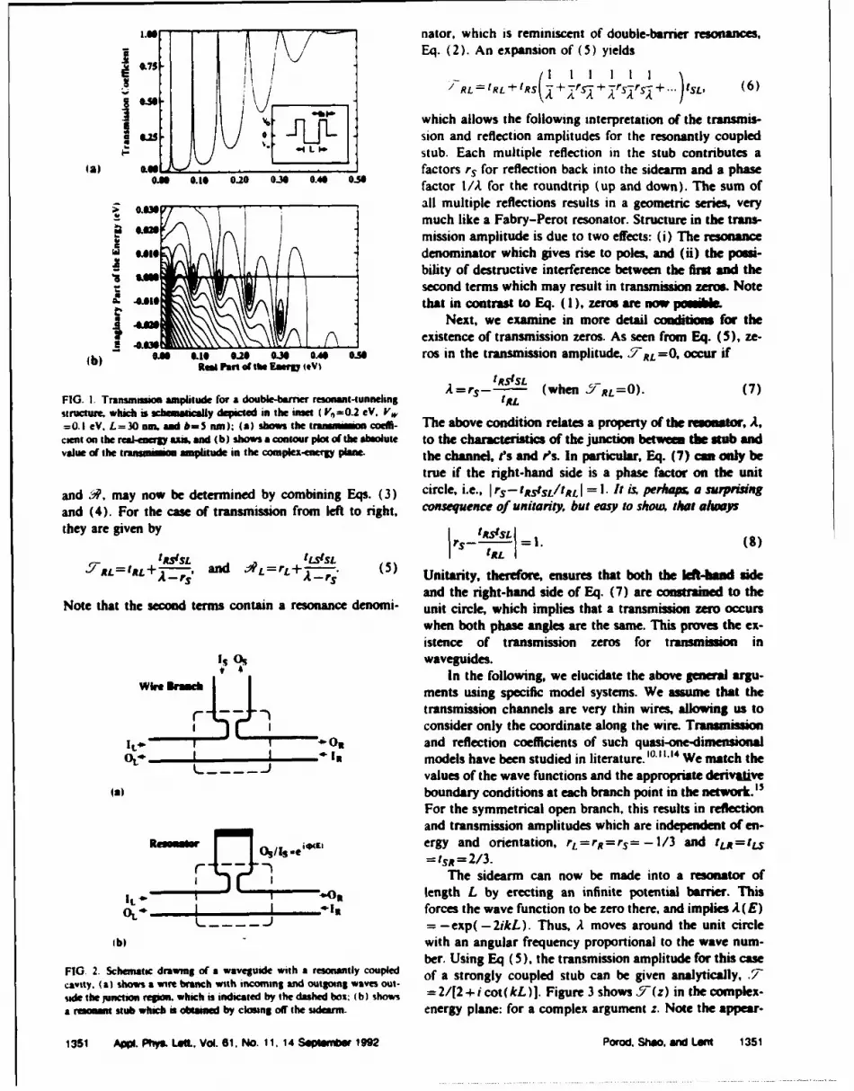
IM nabor, which is reminiscent of double-barnier resonances,£ Eq. (2). An expansion of (5) yields
/ RL[Lt'R +r1-_'~S,-.tL (6)
IO which allows the following interpretation of the transmis-SM sion and reflection amplitudes for the resonantly coupled
I U stub. Each multiple reflection in the stub contributes a12) 0.401 factors rs for reflection back into the sidearm and a phase
GM 0.s 020 OJM 0.0 05 factor I/1A for the roundtrip (up and down). The sum ofall multiple reflections results in a geometric series, very
0.4m much like a Fabry-Perot resonator. Structure in the trans-mission amplitude is due to two effects: (i) The resonancedenominator which gives rise to poles, and (ii) the possi-bility of destructive interference between the fins and thesecond terms which may result in transmission zeros. Note
cc -Colothat in contrast to Eq. (I), zeros are now p P Ib11Next, we examine in more detail conditions for the
existence of transmission zeros. As seen from Eq. (5), ze-
1b) see 0.10 0.z sis 0-0 ros in the transmission amplitude. '7 RL =0, Occur ifRual Part of the Maoro 401
A=r 3--Rts (when YRL=O). (7)FIG. L. Transmission amsplitude for a double-barrier resonan-tunneling 'RtLstructume whichis schematicalydepicted inthe ~ e(Vo=0.2 eV. V~,=0. 1 eV, L = 30 auk aadl b-=5 ina); (a) shw [tie tranmision coeffi-. The above condition relates a property of the resonator, A,cient on the read-enegy axi* and (b) shows a contour plot of the absolute to the cactrsisof the junction between the stub andvalue of the itrnstenin~in unplitude in the CO~cmle-etrgfy plitn. the channel, 's and P's. In particular, Eq. (7) cam only be
true if the right-hand side is a phase factor on the unit
and ýP, may now be determined by combining Eqs (3 circle, i.e., I rS - tRStSLIIRL I = I.- It is, per*apts, a supprusngand (4). For the case of transmission from left to right, consequence of unilanity. but easy to show, Mhat alwaysthey are given by 'RS'SL =1.(a
2_t ttLtSL' n 1
4= L T !SL (5) 1 (8)LJRL=IRL+, ajdA~L-. (5 Unitarity, therefore, ensures that both the left-bad side
and the right-hand side of Eq. (7) are constrained to theNote that the second terms contain a resonance denomni- unit circle, which implies that a transmission zero occurs
when both phase angles are the same. This proves the ex-istence of transmission zeros for transmissio in
I~ SOs waveguides.
win BanchIn the following, we elucidate the above general argu-Wife ~ments using specific model systems. We assume that the
- - -. ~transmission channels are very thin wires, allowing us tor ~consider only the coordinate along the wire Transmission
0.O and reflection coefficients of such quasi-one-dimensionalOto. I I models have been studied in literature. 10. 11. 14 We match the
---- -values of the wave functions and the appropriate derivativea2) boundary conditions at each branch point in the network."1
For the symmetrical open branch, this results in reflectionand transmission amplitudes which are independent of en-
RS. ergy and orientation, 'L=rR='S= -1/3 and ILRt=tLS= sR = 2/3.r The sidearm can now be made into a resonator of
IL length L by erecting an infinite potential barrier. ThisI Iit forces the wave function to be zero there, and implies A (E)
L- - -- = - exp (- VWL. Thus, A moves around the unit circlebt) with an angular frequency proportional to the wave num-
FIG 2.Schmatc dawm ofa wvegidewit a esoanty cupld er. Using Eq (5), the transmission amplitude for this cs
cavity. (a) shows a wire branch with incoming and outgoing waves out-. fasrnl ope tbcnb ie nltcly 7side the junction ego. which is indicated by the dashed box: Mb shows =2/[2 +i cot(kL)1. Figure 3 shows 5(z) in the complex-a resonat stub which is obtained by closing ofr the sidearm. energy plane: for a complex argument z. Note the appear-
1351 Apo. Piyo. Lott., Val. 61. No. 11. 14 Soplinfer 1992 Porod. Shoo.a, a ondwt 1351

Los I.00.
11.711 - 0.75
11.5 \ 05
cu. 0.25
1a) 0.00 (a) 0.00 0.20.0 0.2 0.4 0.6 0.8 1.0 0.0 0.2 0.4 0.6 0.8 1.0
t
j* .0.06(b) 0.0 0.2 0.4 0.6 08 1.0 (b) 0.0 0.2 0.4 0.A 0.8 1.0Real Par of the Energy (0v) Real Par of the Eaergy 40)
FIG. 3. Transmission amplitude for the strongly coupled stub, which is FIG. 4. Transmnssaon amplitude for the weakly coupled stub, which isschematically depeted in the inset: (a) shows the transmission coefficient schematically depicted in the inset: (a) shows the trammiom coefienton the real-energy axis, and (b) shows a contour plot of the absolute on the real-energy axis, and (b) shows a contour plot of the absolutevalue of the irammiaiaon amplitude in the complez-energy plane. value of the transmission amplitude in the complex-energy plane.
ance of transmission zeros on the real-energy axis, and the waveguides, lead to zero-pole pairs of the transmission am-existence of poles in the fourth quadrant of the complex- plitude in the complex-energy plane. The proximity ofenergy plane. The zeros occur at energies for which a these zeros and poles leads to sharp variations of the trans-standing wave forms in the stub, i.e., when k = n. ir/L with mission coefficient with energy. Zeros are a new "animal"n = 1,2,..... Also note that the maxima of the transmission not observed in the usual one-dimensional transmissioncoefficient do not occur at the location of the poles, as for resonances.double-barrier resonant tunneling. This is a particularly We are grateful for stimulating discussions with Dr. S.simple example since the elements of the scattering matrix Bandyopadhyay, Dr. M. Bittiker, Dr. S. M. Goodnick,are independent of energy. Dr. W. Patz, Dr. P. Price. and Dr. M. Sain. This work was
An energy dependence in the elements of the scattering supported, in part, by AFOSR and ONR.matrix may be introduced by weakly connecting the stub to Vanostructure Physics and Fabrcaton. edited by M. Reed and W Pthe channel via a tunneling barrier, as schematically de- Kirk (Academic. Boston. 1989).picted in the inset of Fig. 4. We present numerical results Analogies in Optics and Micro Electronics. edited by W. Van Haenngenfor a tunneling barrier of 0.5-eV height and 1-nm thick- and D. Lenstra (Kluwer Academic. Dordrecht, 1990).ness. Figure 4 shows the transmission amplitude for this 'F. Sols. M. Macucci. U. Ravaioli. and K. Hess, J. Appi. Phys. 66. 3892(1989).weakly coupled stub in the complex energy plane. Note (89. S. Lent. in Computmional Electronic edited by K. Hess. J. P. Leb-again the existence of transmission zeros as predicted by urton. and U. Ravaioli (Kluwer, Boston. 1990). p. 259.Eq. (8). The poles move closer to the real-energy axis 'P. J. Price. IEEE Trans. Electron. Devices 39, 520 (1992).which corresponds to the longer lifetime of the resonant 'P. J. Price. Phys. Rev. B 38. 1994 (1988).states doueto theconthein ngbarier. iTime most str g resnant M. Biittiker. IBM J. Res. Dev. 32. 63 (1988).states due to the confining barrier. The most striking fea- 'T. B. Bahder. C. A. Morrison. and J. D. Bruno, Appl. Phys. Lett. 51.
ture is the occurrence of a zero-pole pair for each quasi- 1089 (1987).bound state. With increasing barrier height, the pole ap- 'S. Datta. Quantum Phenomena (Addison-Wesley, Reading, MA.
proaches the zero which leads to a sharper and sharper 1989).p0 M. Buttiker. Y. Imry, and M. Ya. Azbel. Phys. Rev. A 30. 1982 (1984).transition between a transmission zero and one on the real- "M. Cahay. S. Bandyopadhyny. and H. L. Grubin, Phys. Rev. B 39.
energy axis (compare Figs. 3 and 4). In the limit of an 12989 (1989).infinitely high barrier, the poles and zeros merge which ' D. Kowal. U. Sivan. 0. Entin-Wohlman. and Y. Imry. Phys. Rev. B 42.
corresponds to 7 = I for a completely decoupled stub. 9009 (i9O)."B. Shapiro, Phys. Rev. Lett. SO, 747 (1983).In summary, we have demonstrated that quasibound "C. H. Wu and G. Mahler. Phys. Rev. B 43. 5012 (1991).states in cavities, which are resonantly coupled to quantum 1. E. Avron. A. Raveh. and B. Zur. Rev. Mod. Phys. 60. 873 (1988).
1352 Appl. Phy& Lett, Vol. 61, No. 11. 14 September 1902 Porod, Shao, and Lent 1352

Lateral p-n junctions and quantum wires formed by quasi two-dimensionalelectron and hole systems at corrugated GaAs/AIGaAs interfaces
Wolfgang Porod and Henry K. HarburyDepartment of Electrical Engineering. Universitv o0 Notre Dame. Notre Dame. Indiana 46556
Stephen M. GoodnickDepartment of Electrical and Computer Engineering. Oregon State Universtiv, Corvali, Oregon 97331
(Received 13 April 1992: accepted for publication 4 August 1992)
We report the results of modeling lateral p-n junctions and p-n-p quantum wire structures atcorrugated GaAs/AIGaAs interfaces, using the surface orientation dependent amphotericnature of Si doping. We determine the potential landscape and the electron and hole chargedensities within a semiclassical Thomas-Fermi screening model, and then solve thetwo-dimensional Schrodinger equation using finite elements for the quantized electron and holestates at the heterointerfaces. We demonstrate the formation of a one-dimensional electronsystem confined between two lateral p-n junctions, and discuss the advantages of this structurecompared to conventional electrostatic confinement schemes for fabricating quantum wires.
Recent studies'-4 have shown that Si acts as an am- interesting properties of such structures are the coexisencephoteric dopant depending on substrate onentation during of quasi-two-dimensional electron and hole states next to amolecular beam epitaxial growth of GaAs and AIGaAs. In quasi-one-dimenional electron or hole system.particular, growth on { 100} surfaces invariably leads to Figure 1 shows a schematic drawing of the model cor-n-type doping, while p-type behavior has been reported for rugated GaAs/AIGaAs interface. The compassion andGa-terminated {( I I }A surfaces. These findings have led to layer thicknesses are similar to those used by Ebmer et aL Sthe investigation of lateral p-n junctions at selectively in fabricating a lateral light emitting structure. A 50 umetched and epitaxially regrown V grooves consisting of thick layer of Si-doped Al0 3Ga0.7As is overgrown on a{I Il }A facets on { 100} surfaces. Miller3 demonstrated the semi-insulating GaAs substrate with an etched V-groove.feasibility of lateral GaAs p-n junctions which exhibited The substrate terminates in a (100) plane, whereas thegood diode current-voltage characteristics. By using Si- sidewalls of the V-groove are members of the {( I I }A fain-doped Al0o3Gao.7As rather than GaAs during epitaxial re- ily of planes. As indicated in Fig. 1, n-type doping isgrowth, one may also realize a lateral p-n junction between present for the (100) layers, and p-type doping for thequasi-two-dimezi•al electron and hole systems at the (I I ) layers."i Also shown is the heterointerface betweencorrugated GaAs/AIGaAs interface. Ebner et aL 5 demon- GaAs and AIGaAs. For suitable doping conditions, a two-strated electroluminescence corresponding to the GaAs dimensional electron and hole gas (2DEG and 2DHG,quantum well band gap in such a system, and Harbury respectively) forms along this interface.et aL ' reported calculations which confirmed the existence We use the finite element method and Newton-of a lateral p-n junction between two-dimensional electron Raphson iteration to solve the nonlinear Poisson equationand hole gas systems for Si doping densities in excess of within a Thomas-Fermi screening model for room temper-5x 1017 cm 3 . ature. We assume surface pinning at the Al0.3Ga0.7 As
The ability to fabricate lateral p-n junctions between (100) and (111) facets (0.8 eV separation between thehigh mobility two-dimensional hole and electron gases al- conduction band edge and the Fermi level), and n-typelows for a variety of novel complementary device struc- background doping in the bulk of I X 10' cm- 3 . The de-tures. In previous studies, V-grooves have been employed termination of the two-dimensional conduction and va-for the design of quantum wires.7-1° By utilizing ampho- lence bend edges is a challenging numerical problem which-teric Si in such a V-groove structure, a novel quantum wire requires a highly nonuniform mesh because of the compfi-system may be realized at lateral p-n-p junctions."' This cated geometry and the different doping densities. The re-new way of fabricating a quantum wire with lateral p-n sulting large system of linear equations is solved utilizingjunctions' 2 may offer some advantages compared to band width optimized sparse matrix methods. We alsopresent unipolar structures 1 which use metal gate electro- study the quantum-confined electronic states at the hetero.static confinement or sidewall etching. interfaces by obtaining solutions of the two-dimensional
In this letter, we report our results of modeling both Schr6dinger equation for the calculated potential land-lateral p-n junctions and lateral p-n-p quantum wire struc- scape.tures at corrugated GaAs/A]GaAs interfaces. We deter- We now concentrate on the portion of our model struc-mine the potentWi landscape and the electron and hole ture which is shaded and labeled "p-n Junction" in thecharge densities by solving Poisson's equation within a schematic drawing of Fig. I. Depending upon the dopingsemiclassical Thomas-Fermi screening model. Given a cer- densities in the overgrown AIGaAs layer, the (100) andtam potential prile, we then solve Schrodinger's equation ( 111) heterointerfaces may induce two-dimensional elec-for the quantized states at the heteromterfaces. Among the tron and/or hole systems, respectively. A lateral p-n junc-
1B23 AppL. Phy.. LeM 61(1S). 12 Octobe 1992 0003-6661192/401623-03=.0o K 1992 AmencInmamft of Phyim 1823
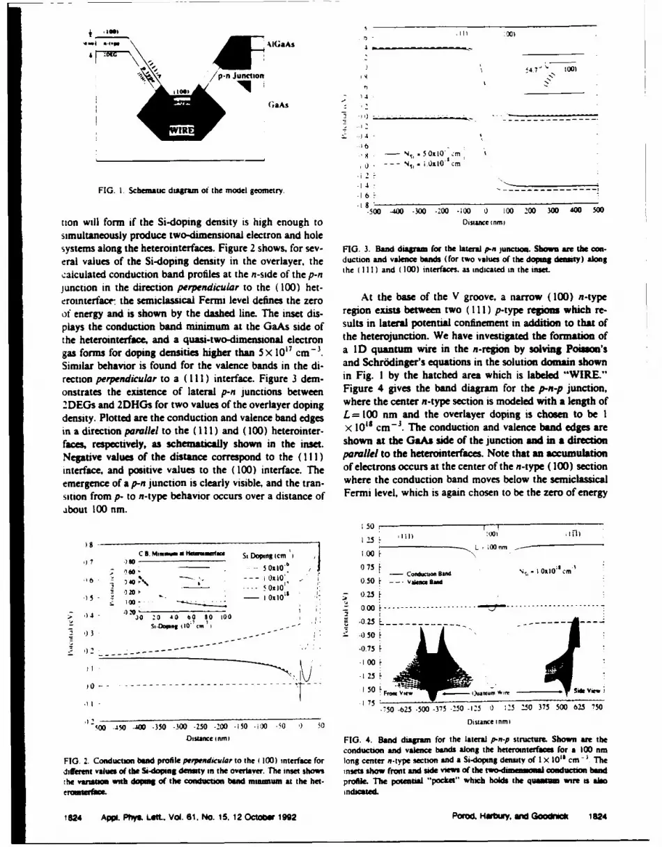
I
4-I .- i. -U4a' -, I00J
/p-n Junction O-
GaAs
-_ --
,__ 0 --- Ns,- ;OxRO 1 Cm
.i2.
FIG. 1 Schemitic diagram of the model geometry. 618
-500 -400 -300 -200 -100 0 100 200 300 400 5ootion will form if the Si-doping density is high enough to Distancehinmi
simultaneously produce two-dimensional electron and holesystems along the heterointerfaces. Figure 2 shows, for sev- FIG. 3. Band diagram for the lateral p-n juncuom. Shown are the con-eral values of the Si-doping density in the overlayer, the duction and valence bands (for two values of the doping density) along
calculated conduction band profiles at the n-side of the p-n the ( I I I ) and (100) interfaces. as indicated in the inset.
junction in the direction perpendicular to the (100) het-erointerfacet the semiclassical Fermi level defines the zero At the base of the V groove, a narrow (100) n-type
of energy and is shown by the dashed line. The inset dis- region exists between two (I ll ) p-type regiois which re-
plays the conduction band minimum at the GaAs side of suits in lateral potential confinement in addition to that of
the heterointerface, and a quasi-two-dimensional electron the heterojunction. We have investigated the formation of
gas forms for doping densities higher than 5X 10"7 cm- 3 . a ID quantum wire in the n-region by solving Poiuuon's
Similar behavior is found for the valence bands in the di- and Schr6dinger's equations in the solution domain shown
rection perpendicular to a ( I 1) interface. Figure 3 dem- in Fig. I by the hatched area which is labeled "WIRE."
onstrates the existence of lateral p-n junctions between Figure 4 gives the band diagram for the p-n-p junction,
2DEGs and 2DHGs for two values of the overlayer doping where the center n-type section is modeled with a length of
density. Plotted are the conduction and valence band edges L = 100 nm and the overlayer doping is chosen to be I
in a direction parallel to the ( 111) and (100) heterointer- x 10s cm- 3. The conduction and valence band edges are
faces, respectively, as schematically shown in the inset. shown at the GaAs side of the junction and in a direction
Negative values of the distance correspond to the ( 11) parallel to the heterointerfaces. Note that an accumulation
interface, and positive values to the (100) interface. The of electrons occurs at the center of the n-type (100) section
emergence of a p-n junction is clearly visible, and the tran- where the conduction band moves below the semiclassical
sition from p- to n-type behavior occurs over a distance of Fermi level, which is again chosen to be the zero of energy
about 100 nm.
150I
7 40C a. MOMOVA a oe r(Mam St D:opig (cm L1]O.O["• , O n
60-- 5O10. , 075 aConlXuoeBMW N ; On10'OCM'•O • i 02K•t0• -- '-•.;.....---- .50 O'ixO 01',5 { - alm•m
*'I '•-~ ~' -1 0.25
0.000 ---- -0 00 ----- -025 -- --------------------
'S ,- 0 _ .. -o0s s '02-------------------- 1 -0-2 --------
3I~ -- -- -050 ~Tfu,2-125
) 0 . . . . . . . . . . . . . . . . *,- - - "1 50 M "e vim'." From Vwew 4.-,- (uMnum *,,•Se•,
,•I-.1 75 -,A'-150 -625 -500 -375-.250-.125 0 125 2.50 375 500 625q 750
it00 .5 . tO0 -350 -300 -250 -200 -i50 -JO -50 ;0 Distance5n0iI
Oistance InmI FIG. 4. Band diagram for the lateral p-n-p structure. Shown are theconduction and valence bands along the heteromnterfaces for a 100 nm
FIG. 2. Conduction band profile perendicular to the ( 100) interface for long center n-type section and a Si-doping density of I X 10'a cm -' The
diffeirent values of the Si-doping density in the overiaver. The inset shows insets show front and side vim of the two-dunenoumal conduction band
the varuitto with dopimg of the conducton bond mmrmnum at the het. profile. The potenial "pocket" which holds the quamm wire is aloerotmatefac. indicted.
1624 Appi. Pht Let. VOL 61, No. 15. 12 October 1992 Porod, H y•,. u Goodrich 1824
_____________________________ * -region is defined by the etch time of the antsotropic: etch* through an optically defined photoresist mask. Thuls, elec-
tron or ion-beam lithography is not required to fabricate- the wire structure. The bipolar nature of the structure may
R-) be utilized to inject minority camers into the wire struc-
ture from the p-regions. which may lead to some interest-______- -ng device applications. Also. if one additionally provided
U sepam itoraphe contrcsol ohe p- and n-type rein usingnaoUX 0 be lihgachieved ro o the wire transport properties could
be achieved both by varying the width of the confinement
- _ -(through reverse biasing the p-a junctions), and through100 -~varying the electron Fermi energy via a gate contact on the
.,1 5 -79.6 mcV AIGaAs above the electron channel.-5 50 I' ;00 __5 s0 *i o :5 _ý ltIn summary, we have demontraedthe existencoe of
Dtsta= nce rugated GaAs/AIGaAs interfaces, which is made possibleby the amphoteric nature of Si-dopants as a Fm F -i of
FIG.S. Potential varianuin penpendicular to the heterointerface (at the crystallographic plane orientations. At V-grooves etchedcenter of the n-type rep) for the two-dimensional conduction band it eiisltn assbtae - uck omprofile shown in Fig. 4. The insets show the wave functions for the lowest inoasmisutng assbtrea- jciofrstwo quantum wire states, which are confined at the GaAs side of the at the intersection of ( 100) and 0Ill) planes if the dopingheterointerface (the darker top portion of the mesh corresponds to the in the overlayer exceeds 5)X 1017 cm -' We have also dem-higher-density AIGaAs overlayer). onstrated the possibility of basing this systemt for the de-
sign of quantum wires which may form at the batom ofand shown as the dashed line. The lateral p-n junctions on the V groove. We find that a quantum wire is to be ex-both sides confine the accumulated electrons in the direc- pected in this p-it-p structure for a length of the n-typetion parallel to the heterointerface. A better perspective of region on the order of 100 nm and a Si-dopin denuuity ofthe two-dimensional potential variation can be gained by I X 10l8 cm-1the insets which present front and side views of the two- The authors would like to acknowledge fruitfu discus-dimensional conduction band profile. Note the dip in the sions with J. Ebner, D. 1. Kirner, C. S. Lent, J. L. Merz,center which defines the "pocket" holding the electrons. M. Mueller, and T. K. Plant. This work has been partially
Figure 5 shows the variation of the conduction band in supported by the Office of Naval Research and the Airthe direction perpendicular to the heterointerface at the Force Office of Scientific Research.center of the n-type (100) region. The sharp dip below the 'semiclassical Fermi level is now clearly visible. The corre- J. MI. Daillinsai and C. E. C. Wood, Appi. Phys. Lect. 411.047 (1982).
~W. 1. Wang. E. E. Mender. T. S. Kuam and L. Esaki. Appi. Phys. Lett.sponding solutions to the two-dimensional Schrdidinger 47. 326 (1985).equation for the pround and first excited one-dimensional 'D. L. Miller. Appi. Phys. Lett. 47.,1309 (1935).subbands are shown by the insets in Fig. S. The peak of the 'S. Subbenna. H. Kroemer. and J. L. Merz J. Appl. Phys. 59. 433,!nvelope function clearly lies in the GaAs side of the het- (1986).
'JI Ebner. J. E. Lary, G. W. Eliason. and T. K. Plant, PovriWda of theerojunction localized between the two p-type regions. (The 20th Eumopean Solid State Device Reearch Confemaev ESSDERC 90darker top portion corresponds to the denser mesh in the edited by W. Ecciestion and P. J. Rossmer (Adam Hiipar. Bisuil, 199).AlGaAs overlayer.) The confinement energies relative to pp. 40-404
the semiclassical Fermi energy are shown schematically on 'H. K. Harbury. W. Porod. and S. M. Goodnick. pruemied at the 19thInternationa Conference on the Physics and Chemistry of' Semionuduc.
the band diagram for the first three levels. The energies tor Interfaces. Death Valley. CA. January 1992.shown all correspond to states originating from the lowest B. I. Miller. A. Shashar. U. Koren, and P.)1. Corvini. Appi. Phys. Lett,two-dimensional subbmnd energy of the heterojunction it K 133 (1939).self. The spacing of the levels, here on the order of 10 meV, 'E. Kapon. D. M. Hwang, andt R. Shat,. Phys. Rev. Lemt 43, 430t"1),,
depends on the doping and the width of the n-region at the andtt. SaSo, 271 Sim9o9y. R ht n .M wn.Ap hbase of the V-groove. As the width is reduced, the subband "E. Colas. S. Simbony. E. Kapon. R. Bhat. D. MI. Hwe and P. S. D.separation should increase, although limitations are im- Lini. Appi. Phys. Lett. 57. 914 (1990).
pose bythelatral xtet o th deletin rgio whch il. K. Harbury and W. Porod. J. Vac. Sci. Technol. 31&.923 (199).pose bythe ateal eten ofthe epltionregon wich I IJ. Ebner (private commuunication).
eventually results wn complete depletion of the wire if made 12 The use of p-m )unctwion for lateral confinement of quenatm wire wastoo narrow. pioneered by C. C. Dean and M. Pepper. J. Phys.C IS. L1287 (1982).
The results above demonstrate the feasibility of realiz- and by A. 8. Fowler. A. Hartstein. and R. A. Webb. Phys. Rev. Lett.ing quntu wie srucureon coruped a~s 1341. 196 (1932).ing quatum irestrutureon acorugatd Gas! NGDIostructUr Physics and Fabneaatoor. MI. A. Reed and W. P. Kirk.
AIGaAs surface. There are several possible advantages of Eds. (Academic. San Diego, 1989).such a structure compared to the current state of the art "The details of the amphoteric nature of the silico, doping nea thewhich relies on sidewall etching or electrostatic confine- intersection of the (100) and (I In surfaces are not keown, and likely
to be more complicated than our model. Thits and pamible coinpemaament from Schottky contacts on the surface of the :tion etlects might tend to reduce the abruqitaam of the W" "- junc-AlGaAs. First, the actaml definition of the width of the tion.
1825 Appl. Ptiys. LIL, VOL 61, No. 15. 12 October 1902 Porod. Hinbury and Goaitnek 1525
Repnnted from JOultU. or Twi ELEcTC"tHMIC,..AL socitVol. 139. No. 10. October t9642
Pnnted in (. S.Copyright 1992
Stability of Thin Resist WallsXiaokang Huang, Greg Bazan, Davide A. Hill,* and Gary H. Bernstein
Department of Electrical Engineering and Department of Chemical Engineerng,University of Notre Dame, Notre Dame, Indiana 46556
ABSTRACT
The physical strength of poly (methyl methacrylate) (PMMA) resist is an important factor for making very densepatterns with most types of lithography. For lines placed closely together using the lift-off technique, a thin wall of PMMAremains to act as the metal line spacer. When placed in contact with a suitable developer, thin polymer walls may swell andbuckle, depending on the desired aspect ratio of the thin walls. We use electron beam lithography and a high-contrastdeveloper solution to study the relationship of the maximum height-to-width ratio of the PMMA walls necessary to avoidbuckling, and the resulting effects on metal thickness after lift-off. Maximum achievable aspect-ratios for our developersystem were found to be constant (nearly 5:1) for widths from 20 to 45 nm and lengths of tens of microns. Theoreticalpredictions based on the hypothesis of a swelling-induced elastic instability are in excellent agreement with the experi-ments.
In the past few years. quantum devices based on ultra- demonstrated with distances between gates of about 100small geometries have received considerable attention. The nm." More recently, optical gratings have been fabricatedusual case involves some feature, e.g., gate length or metal with a metal line pitch of 50 nm over several microns.' Allline width, which is reduced in size in order to observe size such devices require excellent control of line spacing.quantization. In some cases, reduction of line widths plays Because of its uniquely high resolution, poly (methylonly half the role, whereas a decrease in spacing between methacrylate) (PMMA) is among the most important resistsfeatures plays an equally significant part. For example, for nanostructure fabrication. Utilizing the lift-off process,split gates with 100 nm gaps in the form of bends have been the resolution of resulting metal patterns depends not onlymade for the study of transmission properties at corners.' on :he width of the defined lines, which relates to the reso-Also, lateral resonant tunneling transistors have been lution of the beam formation system, but also to the quality
of the edge profile of the resist, which depends to a greatElectrochemical Society Active Member. extent on the contrast of the resist/developer system. The
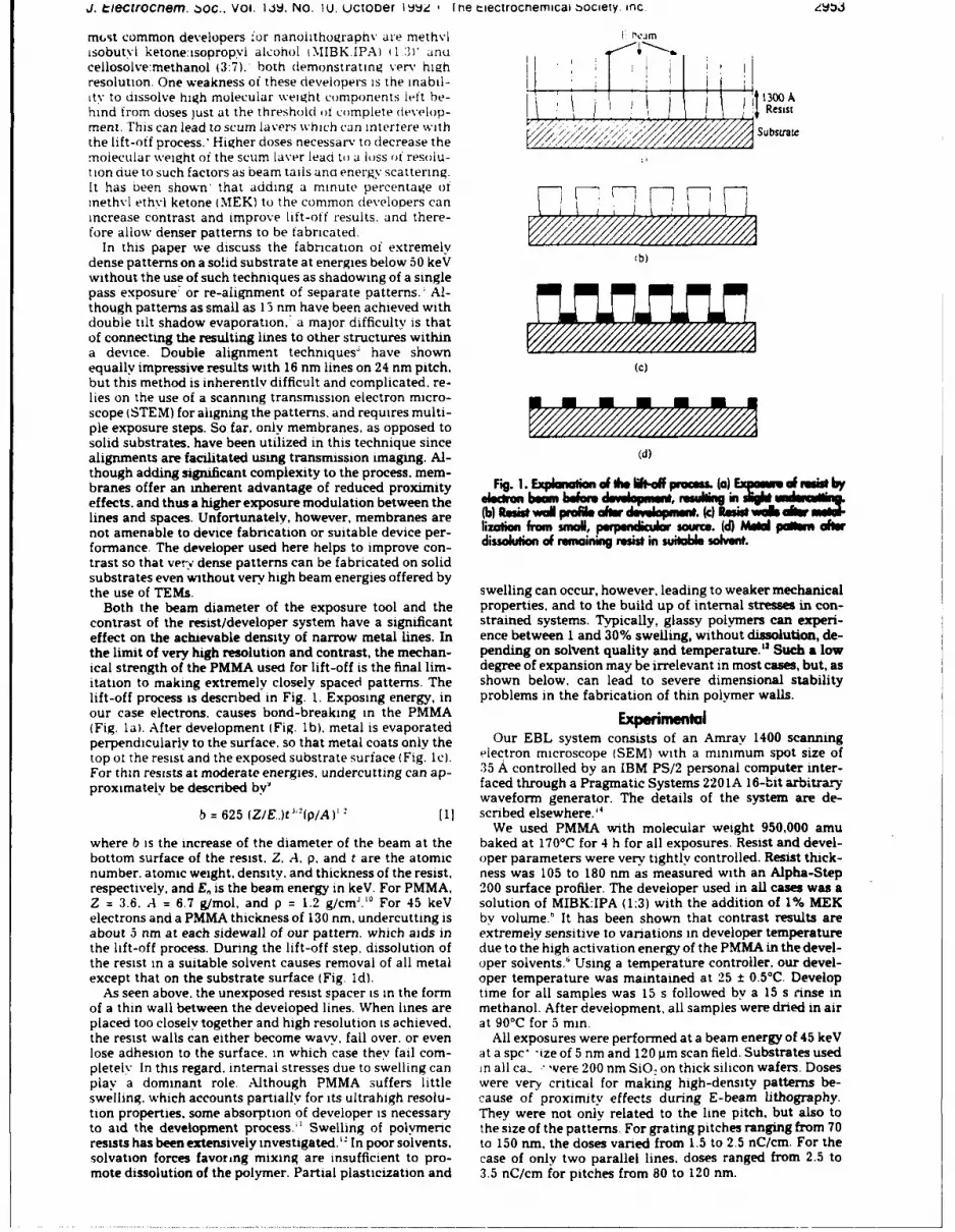
4. tiectrocnem. ,)oc.. vol. l,.s. No. IU. uctooer 1"2, Inre tiectrocnemicai bociety. inc.
mtst common developers for nanoithographv are methylisobutyl ketone:isopropyl alcohol (MIBK.IPA)1 31)' anticellosolve:methanol (3:7). both (demonstrating very highresolution. One weakness of these developers is the inabil-itY to dissolve high molecular weight components left he- 10hind from doses just at the threshold ot complete (ievel)p- Resist
ment. This can lead to scum lavers which can interfere with OW"N//'/ usrtthe lift-off process.: Higher doses necessary to decrease themolecular weight of the scum laver lead to a loss of resoiu-tion due to such factors as beam tails and energy scattering-It has been shown- that adding a minute percentage ot -methyl ethylI ketone IMEK) to the common develop~ers can F7increase contrast and improve lift-off results. and there-fore allow denser patterns to be fabricated.
In this paper we discuss the fabrication of extremelydense patterns on a solid substrate at energies below 50 keV 'b)
without the use of such techniques as shadowing of a singlepass exposure or re-alignment of separate patterns.ý Al-though patterns as small as 15 nm have been achieved withdouble tilt shadow evaporation., a major difficulty is thatof connecting the resulting lines to other structures withina device. Double alignment techniques' have shownequally impressive results with 16 nm lines on 24 nm pitch, (C)but this method is inherently difficult and complicated, re-lies on the use of a scanning transmission electron micro- * m m i i i *scope (STEM) for aligning the patterns. and requires multi-ple exposure steps. So far. only membranes, as opposed tosolid substrates, have been utilized in this technique sincealignments are facilitated using transmission imaging. Al- (d)
though adding significant complexity to the process, mem-branes offer an inherent advantage of reduced proximity Fig. 1. Expkanmtmo of te process (a) of Ibyeffects, and thus a higher exposure modulation between the P1 cl ra bUnt before vlopme, maulg n shlines and spaces. Unfortunately, however, membranes are (b) Res w l profile . (c} e wl p (4
not amenable to device fabrication or suitable device per- lizalion fro small, source. (d) MeW pitam Cher
formance. The developer used here helps to improve con- dissolution of remainng resist in suial solt.trast so that ver-V dense patterns can be fabricated on solidsubstrates even without very high beam energies offered bythe use of TEMs. swelling can occur, however, leading to weaker mechanical
Both the beam diameter of the exposure tool and the properties, and to the build up of internal stresses in con-contrast of the resist/developer system have a significant strained systems. Typically, glassy polymers can experi-effect on the achievable density of narrow metal lines. In ence between 1 and 30% swelling, without dissolution, de-the limit of very high resolution and contrast, the mechan- pending on solvent quality and temperature. 13 Such a lowical strength of the PMMA used for lift-off is the final lim- degree of expansion may be irrelevant in most cases, but, asitation to making extremely closely spaced patterns. The shown below, can lead to severe dimensional stabilitylift-off process is described in Fig. 1. Exposing energy, in problems in the fabrication of thin polymer walls.our case electrons, causes bond-breaking in the PMMA E meni[(Fig. la). After development (Fig. ib). metal is evaporatedperpendicularly to the surface, so that metal coats only the Our EBL system consists of an Amray 1400 scanning
top ot the resist and the exposed substrate surface (Fig. Ic). electron microscope (SEM) with a minimum spot size of
For thin resists at moderate energies, undercutting can ap- 35 A controlled by an IBM PS/2 personal computer inter-
proximately be described by' faced through a Pragmatic Systems 220 1A 16-bit arbitrarywaveform generator. The details of the system are de-
b = 625 (Z/E.,)t ''(p/A)' 2 [1] scribed elsewhere."We used PMMA with molecular weight 950,000 amu
where b is the increase of the diameter of the beam at the baked at 170 0C for 4 h for all exposures. Resist and devel-bottom surface of the resist. Z. A. p, and t are the atomic oper parameters were very tightly controlled. Resist thick-number, atomic weight, density, and thickness of the resist, ness was 105 to 180 nm as measured with an Alpha-Steprespectively, and E, is the beam energy in keV. For PMMA, 200 surface profiler. The developer used in all cases was aZ = 3.6. A = 6.7 g/mol, and p = 1.2 g/cm'."' For 45 keV solution of MIBK:IPA (1:3) with the addition of 1% MEKelectrons and a PMMA thickness of 130 nm. undercutting is by volume.' It has been shown that contrast results areabout 5 nm at each sidewall of our pattern, which aids in extremely sensitive to variations in developer temperaturethe lift-off process. During the lift-off step, dissolution of due to the high activation energy of the PMMA in the devel-the resist in a suitable solvent causes removal of all metal oper solvents.' Using a temperature controller, our devel-except that on the substrate surface (Fig. 1d). oper temperature was maintained at 25 ± 0.5°C. Develop
As seen above, the unexposed resist spacer is in the form time for all samples was 15 s followed by a 15 s rinse inof a thin wall between the developed lines. When lines are methanol. After development, all samples were dried in airplaced too closely together and high resolution is achieved, at 90'C for 5 min.the resist walls can either become wavy, fall over. or even All exposures were performed at a beam energy of 45 keVlose adhesion to the surface, in which case they fail comr- at a spc' -ize of 5 nm and 120 pm scan field. Substrates usedpletely In this regard, internal stresses due to swelling can in all ca.. were 200 nm SiO on thick silicon wafers. Dosesplay a dominant role. Although PMMA suffers little were very critical for making high-density patterns be-swelling, which accounts partially for its ultrahigh resolu- cause of proximity effects during E-beam lithography.tion properties, some absorption of developer is necessary They were not only related to the line pitch, but also toto aid the development process." Swelling of polymeric the size of the patterns. For grating pitches ranging from 70resists has been extensively investigated.'" In poor solvents, to 150 nm, the doses varied from 1.5 to 2.5 nC/cm. For thesolvation forces favoring mixing are insufficient to pro- case of only two parallel lines, doses ranged from 2.5 tomote dissolution of the polymer. Partial plasticization and 3.5 nC/cm for pitches from 80 to 120 nm.

TABLE
/UNSTABLE
/ -WAVY WALLS)
. //
0 20 40 60 80 100 120 140 160 160 200
CnIK&cl mIe"I [rfil
Fog. 2. a m m@ char of a ld wal P. LM Fig. 3. Mkiw widi of PMMA wk awd& for o giaare n VWl &A, wav lr is ve o km, d RAM sw" mW "&dm aI heqiw.
opacity to radiation (e.g., x-rays), etc. We have determinedAll metal evaporations were gold from an electron beam that to achieve reliable lift-off, the thickness of PMMA
evaporator with crucible size of 2.5 cm and a distance of 40 should be at least three times the desired thickness of thecm from the source to wafer. Metal thicknesses were closely small metal pattern. This rule of thumb will depend to somecalibrated with a film thickness monitor and a surface extent on the metal evaporation system. since the physicalprofilometer. All metal thicknesses were 30 ± I nm. Lift-off size of the evaporant source, the source-to-sample spacing,was performed by soaking the samples in acetone for about and the care taken to place the sample perpendicular to and5 mnm. followed by the application of acetone using a hypo- directly above the source will all affect the amount of metaldermic syringe, followed by a 15s methanol rinse, and fuinal deposited on the inside surfaces of the PMMA etched by theblow drying in nitrogen. developer. Using this relationship, and guided by the
Res~b "critical-aspect-ratio" criterion, we fabricated double goldlines with an approximately 20 nm space and a metal thick-
In order to achieve lift-off of evaporated metal films, it is ness of 30 nm, from 105 nm thick resist layers. The linesnecessary that PMMA walls remain between the developed were continuous and straight over a distance of 25 tAm.areas. Assuming minor undercutting for thin resists and Figure 4 shows a portion of these lines at highhigh beam energies, it is expected that the spaces of the magnification.resulting metal patterns closely reflect the width of the re-maining PMMA walls, especially at the top. Because of the Disvissionvery low solubility of unexposed PMMA of very high We begin our discussion with some simple theoreticalmolecular weight,' the height of the walls after develop- considerations about the stability of a long wall with ament is still approximately the same as the initial resist rigidly anchored bottom and a top free end subject to inter-thickness. nal stresses. Comparison with experiments will then
After application and bake. PMMA can be considered a closely follow the theoretical predictions.strong, glassy material. Exposure to the developer, how- The system of interest is shown in Fig. 5. which also givesever. causes swelling of the polymer. leading to the buildup the characteristic geometrical parameters. Mathemati-of internal stresses in strongly anchored structures. Comn- cally, the problem is conveniently formulated within thepressive stresses in the wall can, in turn. lead to buckling, framework of linear plate theory. leading to the following
The wall aspect-ratio (height-to-width) is an important homogeneous boundary value problem for the lateral dis-parameter in delineating the stability threshold. since a placement.tall. thin wall will be strongly susceptible to small dimen-
sional perturbations around the erect position, while a A 2 a'8 +a8 o,,12(l- v2 ) A[
short wall will be able to sustain a higher degree of swelling + 2 P - = - [21before buckling. Figure 2 shows the remaining metal afterlift-off of a typical failed wall. The bright areas are evapo-rated gold. and the dark. wavy center line is the shadow ofthe remaining wall over which gold was deposited and re-moved. The wall was about 30 nm wide and 140 nm high.We show later that a direct relationship exists between theoriginal wail height and the wavelength of the distortion.
Figure 3 shows the minimum width of a PMMA wallachievable for a given starting resist thickness. Error barsrepresent variations in metal line separation (and thereforewail thickness) over the length of the lines. These data wereobtained by smoothly varying the line pitch for a givenresist thickness and observing the point at which lines ei-ther failed completely or became noticeably wavy. Thedata indicate a direct proportionality between critical wallheight and width, implying a constant aspect-ratio forbuckling.
Although the lower the thickness of the PMMA. thecloser the achievable line spacing, the resist thickness can-not be lowered arbitrarily because, for different processes.different thickness of metal are required depending on stepcoverage, line continuity, multiple metal layers, device Rg& 4. Viny dmd Wemd gW Ntes 0 WO Thscaling requirements. electrical resistance constraints. duI m low is 20 .ow er a dll

S. .. vuu,,•.,, ,.*•-, u* *,a.t *V., % .•LuUU%; i,.pe, me r-it~lF.Icrocnemw(,di auc.;et~y, lilt. z-" t
ginal stability limit (indifferent equilibrium), and can becalculated by solving Eq. 10 numerically. We obtain A' =10.40, and 4" = 1.917. Combining these results with Eq. 8and 9. the smallest critical stress. o-. and the associatedwavelength. X. are calculated to be
8(X, y) cT*.z = 26 Ew/1[30(l - vh'] [121h k = h2YU/1.917 [131
For swelling-induced stresses. or, can in turn be obtainedw yfrom
a' = Ee,_ [141
where E,_ is the hypothetical swelling strain that the wallX would undergo if allowed to expand freely. Equations 12
and 14 allow us to calculate the critical wall aspect-ratioOfor stability, (hiw), as a function of the swelling strain
(h' y if[15]wi= \30(1-vir,..
For (hlw) > (hiw)* the wall will buckle. Equation 15 is moreconvenient for comparison with experiments than Eq. 12,since it does not contain the unknown modulus E (which
Fig. S. Dingran o WN, 06n w g presumably changes upon swelling). As expected, a shortpousien used m On analysi wall can sustain a higher degree of swelling before buck-
ling. Additionally, Eq. 15 predicts that, for a constant E.,the critical wall height and width should be directly pro-
6 = 0 at y 0 (no displacement at the bottom) portional to each other. This prediction is in excellentagreement with our data, as shown in Fig. 3.(3) The slope of the line in the figure provides the critical
Saspect ratio for buckling: (hiw)" = 4.75. Calculation of e.- = 0 at y = 0 (built-in bottom end) [4] from Eq. 15 requires knowledge of Poisson's modulus, v.
Because the polymer is swollen, and the stresses are rela-
6 4•:8 tively small, the assumption v = 0.50 is appropriate, giving:+ v a = 0 at y = h (torque-free top) [5] c,, = 5.1%. This value is well within the expected range for
glassy polymers. "
Another easily accessible observable is the wavelength ofA CA the distortion after buckling, X, (Eq. 13). In Fig. 2, the meas-( - 0t hured wavelength of the distortion is 460 nm, which is in
(shear force-free top) [6] excellent agreement with the value of 459 nm given bywhere a. -> 0 is the internal ompressive stress, v Poisson's Eq. 13 with h = 140 nm.whereus. E Young's the e a nd compressivehstres wl tThe maximum amplitude of the lateral dirlAtcement ofmodulus. E Young's modulus, and w and in the wall thick- the wall, A (see Fig. 5), can also be measured by SEM. If weness and height. respectively. For an infinitely long wall the assume that the deformation profile is unaffected by sol-solution to Eq. 2 is of the form vent evaporation, then the observed value of A can be used
S•x. Y) = cos !,/h)iA (sinh(ay/h) - sm(ny/h)) to obtain an independent estimate of E, as follows.The curvilinear contour length between nodal points at
B (cosh(ay/h) - cos(Oy/h))1 [7] the top of the wall after buckling can be calculated from
where A and B are integration constants, and LX(1 +c..)= 1 +( ) 2 smn(z)dz [16]
a A4'(81For (2xA/;)2 << 1 (subject to verification), the kernel inEq. 16 can be expanded up to second-order terms and inte-
o. 12(1 - v-)h grated to give
Variable -, is related to the wavelength of the prevailing = : [ - J [171distortion. 4. as follows This equation can be used to calculate E,,, with the mea-
X = 2.h/l, Is91 sured values of A and K. From Fig. 2 we estimated A -33 nm. giving (with k = 460 nm) E_ = 4.7%. This value is inImposition of the boundary conditions provides the follow- good agreement with the previous estimate of 5.1%. ThesenR equation for the eigenvalues findings confirm that swelling is the dominant mechanism
1 for instability in our experiments. It is remarkable that aits +is- - ti cosh(fa cos(i) = (a't: - Ps* •inh(a) sz(n$) 5% swelling can lead to the failure of a wall less than five
[101 times higher than its width.
'.;;here Summary and Conclusionst = V42 We have investigated the relationship between minimum
[Il I line spacing and maximum metal thickness for EBL-fabri-s = & - v4: cated patterns using high-contrast resists. Both theory and
experiments confirm that a small degree of swelling may.As customary in stability theory. Eq. 10 is satisfied only lead to the catastrophic failure of PMMA walls of relatively
by a discrete set of I values, provided A is greater than or modest aspect-ratio. For subcntical aspect-ratios, linelqual to a miinium crtical value, A'. Phymcally, A' is the spacings as small as 20 nm. and metal thicknesses as high
smallest dimensionless) load necessary to reach the mar- as 30 nm were reliably achieved without loss of adhesion or
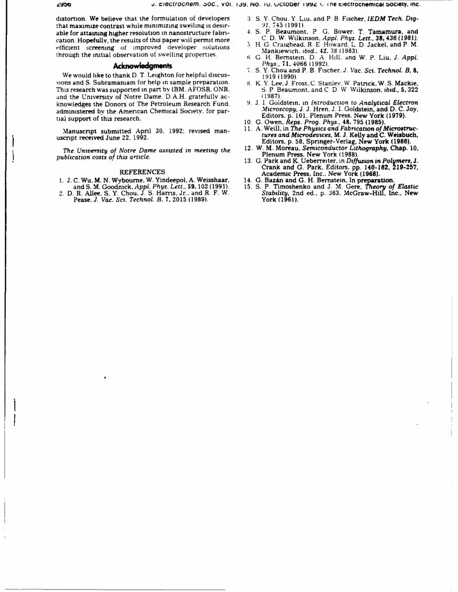
.oo ,j. ciectrocnem. )oc., vol. I JV, No. I u, uctooer i Ut L, i ne •iectrocnemical bOCiety, inc.
distortion. We believe that the formulation of developers Ti S. Y. Chou. Y. Liu. and P. B. Fischer, IEDM Tech. Dig-that maximize contrast while minimizing swelling is desir- W 1. 745 (1991).able for attaimng higher resolution in nanostructure fabri- 4. S. P. Beaumont. P G. Bower, T. Tamamura. andcation. Hopefully, the results of this paper will permit more C. D. W. Wilkinson. Appl. Phys. Lett., 38,436 (1981).efficient screening of improved developer solutions 5 H. G. Craighead. R. E Howard. L. D. Jackel, and P. M.
.Mankiewich. ibid.. 42. 38 (1983).through the initial observation ot swellin properties. 6 G. H. Bernstein. D. A Hill. and W. P. Liu, J. Appi.Ackwwl mentsPhys., 71, 4066 (1992).
7. S. Y. Chou and P. B. Fischer. J. Vac. Sci. Technol. B, 8,We would like to thank D. T. Leighton for helpful discus- 1919 (1990).
sions and S. Subramaniam for help in sample preparation. 3. K. Y. Lee. J. Frost. C. Stanley. W Patrick, W. S. Mackie,This research was supported in part by IBM. AFOSR. ONR. S. P. Beaumont, and C D. W Wilkinson, ibid., 5,322and the University of Notre Dame. D.A.H. gratefully ac- (1987).knowledges the Donors of The Petroleum Research Fund. 9. J. I. Goldstein, in Introduction to Analytical Electronadministered bv the American Chemical Society. for par- Microscopy, J. J. Hren. J. I. Goldstein, and D. C. Joy,"tial support of this research. Editors, p. 101. Plenum Press. New York (1979).
10. G. Owen, Reps. Prog. Phys., 48. 795 (1985).Manuscript submitted April 30, 1992: revised man- 11. A. Weill, in The Physics and Fabrication of Microstruc-
uscnpt received June 22, 1992. tures and Microdevices, M. J. Kelly and C. Weisbuch,Editors, p. 58, Springer-Verlag, New York (1986).
The University of Notre Dame assisted in meeting the 12. W. M. Moreau. Semiconductor Lithography, Chap. 10,publication costs of this article. Plenum Press, New York (1988).
13. G. Park and K. Ueberreiter, in Diffusion in Polymers, J.Crank and G. Park, Editors. pp. 140-162, 219-257,
REFERENCES Academic Press, Inc.. New York (1968).I. J. C. Wu. M. N. Wybourne, W. Yindeepol, A. Weisshaar, 14. G. Bazan and G. H. Bernstein, In preparation.
and S. M. Goodnick. Appl. Phys. Lett., 59, 102 (1991). 15. S. P. Timoshenko and J. M. Gere, Theory of Elastic2. D. R. Allee. S. Y. Chou. J. S. Hams. Jr.. and R. F. W. Stability, 2nd ed., p. 363. McGraw-Hill, Inc., New
Pease. J. Vac. Sci. Technol. B, 7. 2015 (1989). York (1961).

SCANNING 'Voi. 14. 345-34Q i 19L2) Received September 16. 1992S FAIS. Inc.
Determination of Fixed Electron-Beam-Induced Positive Oxide Charge
G.H. BERNSTEIN. S.W. POLCHLOPEK. R. KAMATH. W. POROD
Department of Electrcal Engineenng. University of Notre Dame. Notre Dame. Indiana. USA
Summary: Contrary to previous beliefs, electron-beam- trapped charge can be either positive or negative, depend-induced positive charges in insulators persist where creat- ing on the beam-accelerating voltage, the thickness of theed for at least several weeks without discernible move- insulating layer. and the nature of the substrate. Typically,ment. Formerly. coating with a thin metal overlay was at higher voltages, SEM images of thin insulators on con-thought to allow the charge to leak away. Coating with a ducting substrates appear dark because of trapped positive
conductor is shown to shield electric fields from affecting charges left behind by secondary electrons ejected by thethe imaging probe. but to remove no charge from the spec- primary beam. It is commonly believed that the coating ofimen. A new technique is introduced for the evaluation of insulating specimens by a conductive layer caums this pos-the properties of electron-beam-induced positive charges in itive charge to be drained away from the imaging area, thusmetal-oxide-semiconductor (MOS) capacitors. MOS struc- eliminating distortions of the probe and restoring usabletures were subjected to partial area exposure in a scanning resolution (Goldstein et al. 1981). A nuisance in SEMelectron microscope. These exposures resulted in the cre- imaging. excess positive charge in the gate oxide of metal-ation of areas of localized positive charge within the oxide, oxide-semiconductor tMOS) devices (McLean et al. 1989.which was observed as steps in the capacitance-voltage Nicollian and Brews 1982) can be created by electrondata. A systematic study was performed. It related the beam processing used in certain integrated circuit fabrica-exposed area to the step height and the amount of induced tion and analysis techniques. With electron beam lithogra-charge to the voltage shift of the step. A model describing phy, metal over- or under-layers are used to reduce thethe observed phenomenon is presented, followed by a charging effects during beam writing of nonconductive re-comparison of theoretical and experimental results. The sists (Henderson 1980). The precise properties and behav-progress of the charge over time was studied by perform- ior of the induced charges in insulating films are uncer-ing capacitance-voltage analysis 30 min after electron tain. Although in MOS structures much is known aboutbeam exposure and up to 4 weeks later. the creation. minimization, and annealing of e-beam-in-
duced bulk oxide damage (Balasinski et al. 1988, Keeryet al. 1976. Sah et al. 1983. Shimaya et al. 1983), details ofthe behavior of localized positive charge within oxide lay-ers are not fully understood. This is partly becaumse an easy
Introduction and accurate method to monitor localized oxide charge hasnot been established.
Charging of specimens is a common problem encoun- For the first time we can report that electron-beam-in-tered in the imaging of all insulating materials in a scan- duced positive charges remain fixed where created. To de-ning electron microscope (SEM). In general. the details of monstrate this, we have developed a technique that uses athe charging mechanism can be a complex function of certain structure in the capacitance-voltage (C-V) curves ofbeam and material parameters. Krause and co-workers MOS capacitors. This structure can be used to yield valu-(Krause et al. 1989) have demonstrated that in thin films, able information regarding the location av.'. amount of
charge deposited in SiO2 in a MOS structure. Using elec-tron beam lithography, we accurately exposed partial areasof MOS capacitors with known electron doses. This servedto effectively create two capacitors in parallel, with onemetal gate. having different threshold values due to theinduced positive charge in the oxide. By performing C-V
This work was supported in pat by ONR. AFOSR. IBM. and the measurements before exposure, 30 min afterward, and
later, it was possible to electrically monitor the inducedAddress for reprints: positive charge. The results of these experiments, along
G.H. Bernstein with conclusions about the electrical behavior of the charge
Depanment of Electricai Engineering within the oxide. are reported. A model relating the ex-Universiv of Notre Dame posed capacitor area to the theoretical C-V results is pro-Notre Dame. IN 46556. USA posed and compared with experimental results.

346 Scanning 14. 6 19921
Experiment A. A= A ., A,
The starting material used for MOS capacitor fabrica-tion was <100> orientation. p-type silicon with doping /A
concentration N, = 1.5x 10' cm After caretul clean-ing, the silicon wafers were oxidized at lO000C for 20 min. C
resulting in oxide thicknesses ranging from 738-833 A. asdeduced from the accumulation capacitance of the indi-vidual C-V curves. In order to minimize the effects of mo- (a) (bSFriG. I Schematic diagram of the partial area exposure of a MOSbile ion contamination, oxygen was bubbled through a capacitor. (a) Definition of the exposed area. A. and the unexposedsolution of 2% HCI in deionized water. Circular aluminum area Au. Nb) The exposed and unexposed portions give a total capaci-
dots of an area 4.9X 10⁻³ cm- were evaporated in a high tance. C, which is the sum ofthe two parallel captciuce CQ andCQ.vacuum through a shadow mask onto the surface of theoxidized wafers. The thickness of the Al for all of the dotswas 1.100 A as measured with an Alpha-step 200 pro-filometer. The top surfaces of the metallized wafers were in a fixed positive charge contained in the oxide (Keery etcoated with a protective layer of positive photoresist, then al. 1976, Zaininger 1966, Zaininger and Holmes-Siedleimmersed in a buffered hydrofluoric acid (HF) chemical 1967). The result of this trapped positive charge is deple-etching solution which removed the oxide from the back tion and inversion of the device at more negative voltages.surface. Following photoresist removal, aluminum was C-V measurements were performed on a series of MOSevaporated onto the back surface of the wafers, after which capacitors both before and 30 min after partial area expo-the wafers were annealed in flowing nitrogen gas for 20 sure in an SEM, as described above. Figure 2 shows typicalmin at 420"C. results obtained from two of these capacitors that have frac-
Partial areas of the completed MOS capacitors were tional exposure areas, Ae/At, where Aý is the exposed areasubjected to electron beam exposure as shown schemati- and At is the total area, of 10.4 % and 62.4%, respectively.cally in Figure Ia. changing the device properties where The relevant features in this figure are the additional stepsexposed and thus effectively dividing the device into two in the C-V curves observed after exposure. Comparison ofseparate capacitors in parallel, as described in Figure lb. Figures 2a and 2b shows that the step height increases forExposures were performed at 20 kV and 0.8 nanoamperes larger fractional area exposure but the location of the step isin an Amray model 1400 scanning electron microscope. approximately the same for constant areal dose.The SEM was controlled using a Pragmatic Instruments We demonstrate below that our observed steps are duemodel 2201 A arbitrary waveform generator and custom to trapped positive charge in the exposed area. which caus-software to ensure dose and area accuracy. Exposures were es that area to deplete and invert at more negative voltagesexecuted by quickly imaging a single capacitor at a very than the unexposed portion of the capacitors. Althoughlow current. blanking the beam. setting the current to the steps have been previously reported in C-V data after elec-desired value, and scanning (using e-beam lithography) a tron beam irradiation, they were of different origin. In asquare of known area entirely within the MOS capacitor. study of Zaininger (1967). steps were observed after totalThe dose was fixed at 4 X 10- 5 C/cm2. and exposed areas capacitor exposure and were attributed to the enhancementranged from 10.4-62.4% of the total area of the capacitor. of existing interface states concentrated around a singleThe upper limit on areal exposures was determined by the energy level in the band gap. When the degree of perfec-size of the largest possible inscribed square within a circle tion of the interface was high. no step was observed, buti with area ratio 2/nt. the entire C-V curve was shifted to more negative voit-
ages. In order to test whether our steps were due to such asurface state phenomenon. we performed whole area expo-
Results and Analysis sures of our capacitors. The results of our test are shown inFigure 3. The shift of the C-V characteristics with no step
Total electron beam exposure of high quality MOS present indicates that our steps in the partial exposuredevices is known to cause a negative shift of C-V charac- experiments are not related to the enhancement of pre-teristics (Johnson 1975. Keery et al. 1976. McLean et al. existing intertace states but are a result of the localized1989. Nicollian and Brews 1982. Sah et al. 1983. Shimaya positive charge created in the exposed area.et al. 1983). Free electrons created in the oxide during ex- We now develop a quantitative model. which relates theposure either recombine with holes or leave the insulator: size of the observed steps to the areas of exposures, assum-thus they are electrically eliminated (Keery et al. 1976. ing that the created positive charge is fixed where created.Zaininger and Holmes-Siedle 1967). Holes. however, be- A single capacitor subjected to partial area exposure can behave differently because of their much lower mobility in modeled as two capacitors connected in parallel: oneSiO 2 . as some will recombine with electrons, while a sig- capacitor. Ce, with an area equal to that of the exposednificant fraction is captured in stationary traps. resulting area. and another. Cu, with an area equal to that of the un-

G.H. Bernstein et aL: Electron-beam-induced positie charge 347
2801 " I . 1 280Before exposure Before exposure
240 240
20% 200 -.
8 ,AeAfter exposureo16C
L) - - - - - -- - - --
80-8After exposure
40 40
0, 0-25 -20 -15 -10 -5 0 5 10 -25 -20 -15 -10 -5 0 5 10
Voltage VoltageFIG. 2 C-V characteristics of MOS capacitors before and after e-beam partial area exposure. The exposure areas were (a) 10.4% and (b)b2.4% of the total area.
exposed area. Since the exposed area has a more negative sider the following relations as derived from basic MOS C-threshold voltage. Vie, because of the presence of the pos- V theory (Pierret 1983). The accumulation capacitance ofitive charge in the oxide, it undergoes depletion and inver- the exposed area is given by,sion. while the unexposed area is still in accumulation. Theunexposed area inverts at the unchanged threshold volt- C (I._age. Viu. Figure 4 shows schematically a C-V curve, which do,is a superposition of the individual C-V curves for thecapacitors Ce and Cu. The additional step observed in th where cox is the dielectric constant of SiOz. £o is the vacu-
capaitos CandCu. he dditona ste oberve inthe um permittivity. and do, is the oxide thickness. Simnilarly,experiments is expected to occur at the threshold voltage ot urn pemitoivity.rand pacithe ox thckess. arly.the exposed area. The height of the step should be equal to thersiondcto capactne os ethe difference between the accumulation capacitance. C,. inversion can be expressed as:and the inversion capacitance. C.e, of the exposed area.
To determine the theoretical relationship between the C _=sFrAstep height, C. - C.,, and the exposed area. A,, we con- W (2)
280 Capacitance
Before exposure240
-- -- -- Cat Cae Ca,.
200
* 160 After exposure
= " C W - C "•120
80 "----..........-- .--.... C, = C.e + C"'
40 I C, •
V,0 Vot0 FIG. 4 Schematic diagram ot the C-V curve resulting from partial
-25 -20 -15 -10 -5 0 5 10 area exposure. Key: C = capacitance. with subcripts a =accumula-Voltage iton. t = total. e = exposed. u = unexposd, and a - ,aver.on. V,, ad
FIG. 3 C-V characteristics of a MOS capacitor before and 30 min V," are threshold voltages for exposed anid unexposed portions. re-a.fter total e-beam area exposure. specuvely

.48 Scanning 14. I 1992)
where K,, is the dielectric constant of silicon and W is the maxi- 0.5 'mum depletion-la.er width into the semiconductor. The capac- Theoretical for average a,itance of the exposed area in inversion can now be expressed 0 Theoretical for measured do..is the series combination of the above two capacitances: 0 E
Cie= t31 0.3
The total accumulation capacitance is: 0.0.2
Cal- dK A (4)
0.1
where A, is the total capacitor area. Thus. combining allof the above equations. we obtain a linear relationship be-tween the step height and the exposed area: 0.0 . 0 0 . 0 0 0 0.0.0 0.1 0.2 0.3 0.4 0.5 0.6 0.7
C C K5 A 0 /A,C K (5) FIG. 5 Plot of theoretical and experimental results relating the ex-posure area to the resulting step in the C-V characteristics. Thewhere crosses with error bars indicate experimental dam. The filled circles
represent the predictions of our theoretical model using the actual
K = f oxide thickness for each case. The solid line shows the linear rela-
+ K, d ti onship of Eq. (5) for the average oxide thickuiess of d." = 766 A.
Figure 5 compares the experimental data, obtained 30 change over the 4-week period, implying that no measur-min after exposure. and the theoretical predictions from able diffusion of charge has taken place.Eq. C5). Shown is a plot of the normalized step heigha , (C.T- Even though the charge did not spread out, its magni-CeYCr, versus the normalized exposure eta, Ae/At. The tude decreased over time. The amount of charge dissipa-error bars in the experimental data represent uncertainty in tion can be determined from simple MOS theory. The shiftthe sharpness of the steps. For each individual capacitor in the threshold voltage of the exposed area. AVt,, is relat-with a certain exposed area. we also show the theoretical ed to a change in the oxide charge. AQo,, by:prediction from Eq. (5) for the step height. taking into ac-count the precise value of the oxide thickness for the calcu- - AQO (6)lation of the constant. K. The straight line shown in the AV -Cfigure represents the relationship of Eq. (5) for a value ofK corresponding to an average oxide thickness of 766 A.
Figure 5 gives excellent agreement between our exper-imental results and the above theoretical model, which 280assumes that the positive charge remains fixed in the areawhere it is created. The step height in the C-V data maythus be used as a measure for the areal extent of positive -40charges in insulators. In particular, the out-diffusion of'pos- 200ttve oride charlges may be monitored as a change ot thestep height in time.
To gain further insight into the time-dependence of the Y 160
positive oxide charge. we performed an experiment to de-termine its position and magnitude a significant time after 120 eits creation. We analyzed the C-V data 30 min. 2 weeks. o eoe U~sr1and 4 weeks after partial area exposure of an MOS capac- 80 After exposure
.. - 10 Min.
itor. where the exposed area was 41.6% of the total area. 2 WeeksThe chip containing this capacitor was stored at room tem- 40 Weeksperature in a dark shielded box during the 4-week timeperiod. Figure 6 shows the before- and after-exposure 25 -20 -15 -10 -5 0 5 10curves. We see that the step observed 30 nun after expo- Voltgsure has moved approximately 0.8 volts in the positive FIG, C.VcharactemcsofaMOScapacitorbeforeexposweaddirection after 2 weeks, but only 0.2 volts more after an 10 mm. 2 weeks, and 4 weeks after 41 6% of the total area was ex-additional 2 weeks. Note that the step height did not posed with an electron beam.

(iH. Bernstein er ai:. Electron-beam-induced positie charge 349
The shitt in the threshold ýoltage ot - 14.5 volts 30 mm imaging site but rather bv the electncal shielding of theafter the exposure corresponds to an induced charge den- ,ite by a ground plate.,itv ot 6.8, 10- C/cm:. After 2 wveeks. the charge is re-duced b% only about 6% to 6.4 X I) - C/cm-. After an ad-ditional 2 weeks. the charge is further reduced a mere Acknowledgments1.5%. Positive fixed charges in the oxide can be consid-ered nearly "'permanent" in the absence of any annealing The authors thank Mr. Robert J. Minniti. Jr.. and Mr.treatments. In fact. Zaininger ( 1967) observed that posi- Malay Kundu for assistance with measurements and datative charge can endure for several months in capacitors acquisition, and Mr. Greg BazAn for electron beam lithog-wholly exposed to electron radiation. raphy exposures. We are grateful to Prof. Stephen J.
One might theorize a mechanism by which induced pos- Krause and Prof. David C. Joy for helpful discussions.itive charge is not fixed in the oxide but, in fact, leaks outover a small distance onto the ungrounded metal (i.e., elec-Irons into the oxide), causing a bending of the band struc-ture for the two materials and resulting in a cessation of Referencescharge transfer after some time. Such a mechanism mightcharge dtraferataler syom teimue. aSouh latmehanm ro tin Balasinski A. Jakubowski A. Swit A: The influence of electronnot be detectable by our technique, as our lateral resolution beam energy on defect density in MOS device quality oxides.is obviously limited and the oxide is very thin. However. if Vacuum 38, 1041-1043 (1988) -
this were the case. the metal probe used in the C-V mea- Goldstein JI. Newbury DE. Echlin P. Joy DC. Fion C, Lifshin E:surement would quickly drain the charge for the metal and Scanning Electron Microscopy and X-Ray Microanalysis.allow a continued leakage of charge to the C-V measure- Plenum Press. New York (1981) 461-494mert system. Presumably. such a leakage would be expect- Henderson RC: Device fabrication by electron beam lithography. In
n Electron Beam Technology in Microelectronic Fabrication.ed to act rapidly since in an SEM. sample charging is ap- (Ed. Brewer GR) Academic Press. New York (1980)226-227parently controlled on time scales of the order of screen Johnson WC: Mechanisms of charge build-up in MOS insulators.refresh rates. that is. a matter of a few seconds or less. IEEE Trans Nucl Sci NS-22. 2144-2150 (1975)
Keery WJ. Leedy KO. Galloway KF: Electron beam effects onmicroelectronic devices. Scanning Electron Microscopy. ProcWorkshop on Microelectronic Device Fabrication with the
Conclusko SEM. liT Research Institute. Chicago (1976) 507-513Krause SJ. Mohr J. Bernstein G. Ferry DK. Joy DC: A new method
We have shown that partial area exposure of MOS ca- for measuring the thickness of thin film insulators. Proc Micro-pacitors using electron beam irradiation results in the cre- beam Analysis Soc 14. 459-462 (1989)
McLean FB. Boesch HE Jr. Oldham TR: Electron-hole generation.ation of an area of immobile positive charge within the transport. and trapping in SiO.. In Ionizing Radiation Effects inSiO2 layer. This charge causes depletion and inversion of MOS Devices and Circuits (Eds. Ma TP. Dressendorfer PV)the exposed area of the capacitor at more negative volt- John Wiley & Sons. New York (1990) 87-92ages than the unexposed area. which resulted in a step in Nicollian EH. Brews JR: MOS (Metal Oxide Semiconductor)the C-V characteristics. A systematic study of exposed Physics and Technology. John Wiley & Sons. New York (1982)
549-553area as a function of step height indicated that step height Pierret RF: Field effect devices. Modular Series on Solid Stateincreased with increasing exposure area. After a theoretical Devices 4. Addisoa-:Wesley, ( 1983) 43-80model had been proposed. experimental results were com- Sah CT. Sun JYC. Tzou ]IT: Effects of keV electron radiation on thepared with those obtained from this model. The good avalanche-electron generation rates of three donors on oxidizedagreement we obtained demonstrated a direct correlation silicon. J Appl Phvs 54. 1563-1568 (1983)
Shimaya M. Shiono N. Nakajima 0. Hashimoto C. Sakakibara Y:between the exposed area and the step height in the C-V Electron beam induced damage in poly-Si gate MOS structuresdata. We exploited this phenomenon to show that the pos- and its effect on long-term stability. J Electrochem Soc 130,itive oxide charge does not diffuse over long time periods. 945-95011983)This demonstrates that in electron microscopy, the corn- Zamninger KH: Irradiation of MIS capacitors with high energy elec-
trons. IEEE Trans Nucl Sci NS- 13. 237-247 (1966)mon technique of coating nonconductive substrates with a Zaininger KH. Holmes-Siedle AG: A survey of radiation effects inmetal overlayer in the case of positive charging is accom- metal-insulator-semiconductor devices. RCA Review Juneplished not by the draining of excess charge away from the 208-24001967)
Swelling and surface forces-induced instabilities in nanoscopic polymericstructures
Davide A. Hilli)Department of Chemical Engineering, University of Notre Dame. Notre Dame, Indiana 46556
Xiaokang Huang, Greg Bazan, and Gary H. BernsteinDepartment of Electrical Engineering, Unnwersity of Notre Dame, Notre Dame. Indiana 46556
(Received I May 1992: accepted for publication 12 July 1992)
For closely spaced, nanolithographically defined lines, a thin wall of re st remains to act as themei A line spacer. When exposed to a developer, and then rinsing solution, closely spaced resistwalls may become unstable as a result of two effects: (1) internal stresses due to swelling, and(2) lateral surface forces between adjacent walls. In this article we perform a linear stabilityanalysis of a thin polymer wall under the simultaneous action of internal stresses and lateralsurface forces. We calculate a stability boundary, and show that internal stresses are necessaryfor the formation of deformation patterns of finite wavelength. We find that, for slightlysubcritical swelling stresses a small lateral force can induce buckling, while, for slightlysubcritical surface tractions large internal stresses are necessary to induce instability.The theoretical predictions are in good agreement with experimental data onpoly (methyl-methacrylate) walls produced by electron beam lithography.
INTRODUCTION number, atomic weight, density, and thickness of the resist,In addition to ultrahigh resolution, an important as- respectively, and E=. is the beam r. in ke. For
petIfnanfbiainfrnneeto si h civ PMMA, Z= 3.6, A = 6.7 g/mol, and p= 1.2 g/cm'.' For 45pect of nanofabrication for nanoelectronics is the achiev- keV electrons and a PMMA thickness of 130 rin, under-
able spacing of metal features. Extremely closely spaced cutting is about 5 nm at each sidewall of our pattern, which
features have been utilized in such devices as lateral tun-
neling transistors,' split gates, 2 and optical gratings. 3 In aids in the lift-off process.applications such as these, metal features are required with As discussed above, the unexposed resist spacer is inspaces atios a few hundred A. The fabrication of very the form of a thin wall between the developed lines. Whenspacew gaps s oavera aapfewehundred a.ce f a f ver lines are placed too closely together and high resolution isnarrow gaps over appreciable distances (a few pm) re- achieved, the resist walls can either become wavy, fall over,
quires very good control of lithographic processing param- orheve d h the surace, in whichcasethevfaieters. or even lose adhesion to the surface, in which caw they fail
Mc st pattern transfer in nanolithography for quantum completely. In this regard, internal stresse due to swelling
devices is effected by the lift-off process in which a thin and lateral surface forces between adjacent structures can
metal layer is deposited by perpendicular, thermal evapo- play dominant roles. Although PMMA suffers little swell-
ration onto a resist [usually poly (methyl methacrylate) ing, which accounts partially for its ultrahigh resolution
SPMMA)] such that metal falls either on the surface of the properties, some absorption of developer is necessary to aid
undeveloped (positive) resist or onto the surface of the the development process.b Swelling and solubilization of
substrate where exposed and developed resist has been re- polymeric resists have been extensively investigated.7'- In
moved. Subsequent removal of unexposed resist also re- marginally poor solvents, solvation forces favoring mixing
moves all metal except that on the surface of the substrate. are insufficient to promote dissolution of the polymer. Ap-When metal patterns are to be placed very closely together, preciable swelling can occur, however, leading to weakerthe space is formed by the shadowing of the deposited mechanical properties, and to the buildup of internalmetal by a thin "wall" of resist. We report here on the stresses in constrained structures. Amorphous polymers offundamental limitations of solvent/PMMA interactions high molecular weight may typically experience betweenwhich lead to failure of the thin features necessary to per- 0.1% and 30% swelling, without solubilization, dependingform lift-off of very closely spaced features. on solvent quality and temperature.8 With mixtures of sol-
For thin resists at moderate energies, undercutting by vents, the swelling behavior can be of considerable com-beam scattering within the resist can approximately be de- plexity, since preferential partitioning of one or more com-scribed by: 4 ponents of the mixture in the polymer can occur. This
would be the case for most resist developer solutions,b=625(Z/Eo')t"2 (p/A)"12 . (1) which usually comprise more than a single component.
Notwithstanding their valuable insight, thermodynamicwhere b is the increase of the diameter of the beam at the models have enjoyed only limited success in the quantita-bottom surface of the resist. Z. A, p, and t are the atomic tive prediction of solubility properties of multicomponent
polymer-solvent systems, and such an attempt will not beA uthor to whom correpondence should be adremed. made here. Nevertheless, as a discriminator of the quality
4056 J Apo. PhVy 72 (9), 1 November 1992 0021-8979/92/214088-07S04.00 e, 1992 American Institute of Physics 4088

of the model, our predictions will be required to compare 3favorably with typical swelling data. 
Recent experiments have considerably clarified the 021 d/p= 3 2 13 1mechanism of interaction between polymeric surfaces. .
Studies of this nature have recently become possible thanksto the perfecting of the surface force apparatus by Is-raelachvili and Tabor.9 In this system. the separation be- ,
tween two mutually orthogonal, cylindrical mica surfaces 0 0 oonto which polymer is adsorbed can be measured with !resolution better than 5 A. The separation measurements
rely on interferometry, while knowledge of the flexural n-gidity of the instrument enables calculation of the forcebetween the surfaces. Normalization of the force by 21r -0.2-times the mean radius of curvature of the mica sheets di-rectly yields the surface energy of interaction.10 Experi- -0.3ments show that in good solvents, polymer surfaces always -3 -2 - 1 0 1 2 3repel each other due to the tendency of the chains to mixmost favorably with solvent molecules. Conversely, in poor 8/psolvents chain-chain interactions are more favorable, lead-ing to strong long-range attraction. Experimentally, theattractive forces between polymer layers become significant FIG. i. Schematic representation of the potential energy of interaction ofwithin a distance of about twice the radius of gyration of a polymer surface confined between and equwdistant from two other sur-
faces. As the dimensionless separation dip mcreaun, the curves broadenthe chains, which can extend to several hundred , for high and the equilibrium position around 6/p=O becomen mdNO , - to maimolecular weight polymers.' 0 Common post-development lateral diaplacements. At very small separatim the plimMi m besm.rinsing solutions are, by design, of poor thermodynamic purely repulsive. At intermediate separains the eret positiomay eithe
quality. Therefore, in addition to swelling, attractive forces be stable or unstable depending on the rigidity of the well.
are expected to play a vital role in the failure of polymeric
nanostructures. All metal evaporations were gold from an electron
beam evaporator with thicknesses of 30* 1 nm. Lift-offEXPERIMENT was performed by soaking the samples in acetone for about
Our electron beam lithography (EBL) system consists 5 min, followed by the application of acetone using a hy-
of an Amray 1400 scanning electron microscope (SEM) podermic syringe, followed by a 15 s methanol rinse, and
with a minimum spot size of 35 A controlled by a personal final blow drying in nitrogen.
computer interfaced through a Pragmatic Systems 2201A16-bit arbitrary wave form generator. We used PMMA THEORY
with molecular weight 950 000 amu baked at 170 "C for 4 The interaction energy between two opposing surfaces,h for all exposures. Resist and developer parameters were z. can be obtained by linear superposition of long-range,very tightly controlled. Resist thickness was 105-180 nm attractive, and short-range, repulsive interactions. Gener-as measured with an Alpha-Step 200 surface profiler. The ally, the potentials are individually modeled as a power-lawdeveloper used in all cases was a solution of MIBK:IPA of the reciprocal of the separation distance, r, giving(1:3) with the addition of 1% (MEK) by volume."' It has (within an arbitrary additive constant):it0J 2
been shown that contrast results are extremely sensitive tovariations in developer temperature due to the high acti. Y=* [ (p/r)a- (p/r)b], (2)
vation energy of the PMMA in the developer solvents." where 1* and p characterize the strength and width of theUsing a temperature controller, our developer temperature potential well, respectively, and a and b (a > b) prescribewas maintsined at 25 +0.5 *C. Develop time for all samples the rate of growth and decay of repulsive and attractivewas 15 s followed by a 15 s rinse in methanol. After de- interactions, respectively. For a polymer wall confined be-velopment. all samples were dried in air at 90 C for 5 min. tween, and equidistant from two parallel surfaces with sep-
All exposures were performed at a beam energy of 45 aration d. the following approximation is appropriate:keV at a spot size of 5 nm and 120 Mim scan field. Sub-
strates used in all cases were 200 nm SiO, on thick silicon Y=.*{[ 1p /(d 2 -62 ) I]/ 2 -[p 2/(d2 -62)1 jZ}
wafers. Doses were very cntical for making high-density
patterns because of proximity effects during e-beam lithog- (for -d<6<d), (3)
raphy. They were not only related to the line pitch, but also where 1, is the surface energy (energy/area), and 6 anyto the size of the patterns. For grating pitches ranging from virtual lateral displacement away from the planar config-70 to 150 nm. the doses vaned from 1.5 to 2.5x 10-" uration. Note that 6, and hence 1,2 will in general varyC/cm. For the case of only two parallel lines, doses ranged from point to point along the surface of the wall. Figure Ifrom 2.5 to 3.5 x 10 C/cm for pitches from 80 to 120 schematically illustrates the shape of 1, for different valuesnm. of the dimensionless separation. dip. It is seen that for
4089 j. Appl. Phys.. Vol 72. No. 9. 1 November 1992 Hill of a. 4089
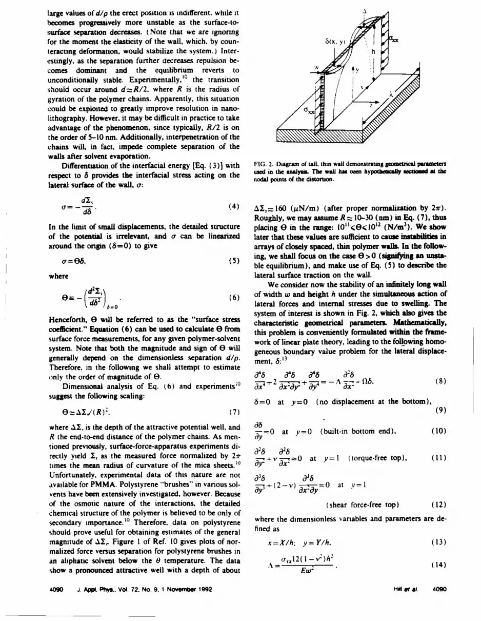
large values of d/p the erect position is indifferent, while it A
becomes progressively more unstable as the surface-to-surface separation decreases. (Note that we are ignoringfor the moment the elasticity of the wall, which, by coun- vI
teracting deformation, would stabilize the system.) Inter-estingly, as the separation further decreases repulsion be-comes dominant and the equilibrium reverts to yunconditionally stable. Experimentally,' 0 the transitionshould occur around d=R/2, where R is the radius ofgyration of the polymer chains. Apparently, this situationcould be exploited to greatly improve resolution in nano-
lithography. However, it may be difficult in practice to takeadvantage of the phenomenon, since typically, R/2 is onthe order of 5-10 nm. Additionally, interpenetration of thechains will, in fact, impede complete separation of thewalls after solvent evaporation.
Differentiation of the interfacial energy [Eq. (3)) with FIG. 2. Diagram of tall, thin wall demonstrating geometrical parameters
respect to 6 provides the interfacial stress acting on the used in the dlsmto rThe w has ron. hypoacagy scimW at thlateal srfae ofthewall a:nodal points of the distortion.
lateral surface of the wall, a':
dX,-dl (4) 12,= 160 (piN/m) (after proper normalization by 210).Roughly, we may assume R = 10--30 (urn) in Eq. (7), thus
In the limit of small displacements, the detailed structure placing E in the range: 1011<e< 1012 (N/M 3). We showof the potential is irrelevant, and a can be linearized later that these values are sufficient to cause instabilities inaround the origin (6=0) to give arrays of closely spaced, thin polymer walls. In the follow-
a=06 (5) ing, we shall focus on the case e>0 (signifying an unsta-ble equilibrium), and make use of Eq. (5) to describe the
where lateral surface traction on the wall.We consider now the stability of an infinitely long wall
e d- ,- (6) of width w and height h under the simultaneous action of
- /=0 •6) lateral forces and internal stresses due to swelling. Thesystem of interest is shown in Fig. 2, which also gives theHenceforth. e will be referred to as the "surface stress characteristic geometrical parameters Mathematically,
coefficient." Equation (6) can be used to calculate e from this problem is conveniently formulated within the frame-
surface force measurements, for any given polymer-solvent work of linear plate theory, leading to the following homo-
system. Note that both the magnitude and sign of e will eous o undar vale problem fo the llo displace-geneall deendon he imenionesssepraton ~p. geneous boundary value problem for the lateral displace-
generally depend on the dimensionless separation dip. ment, 6:13
Therefore. in the following we shall attempt to estimate
only the order of magnitude of 0. d"6 1 8 `66'3Y. Y x_(8)
Dimensional analysis of Eq. (6) and experimentsl 0 x ---•-,-2 -j-p= -- A ax -,f16
suggest the following scaling: 6=0 at y=O (no displacement at the bottom),
O=,/(R). (7) (9)
where 11, is the depth of the attractive potential well, and 6 at y=O (built-in bottom end), (10)R the end-to-end distance of the polymer chains. As men- ay 0
tioned previously, surface-force-apparatus experiments di-rectly yield 1, as the measured force normalized by 21r +v-- =0 at y=l (torque-free top), (11)times the mean radius of curvature of the mica sheets.' 0 -TY- x
Unfortunately. experimental data of this nature are not a336 C116available for PMMA. Polystyrene "brushes" in various sol- ±(2-v) --- =O at v=1vents have been extensively investigated, however. Because a? ayof the osmotic nature of the interactions, the detailed (shear force-free top) (12)chemical structure of the polymer is believed to be only ofsecodar imortnce~° Tereore dat onpolstyene where the dimensionless variables and parameters are de-secondary importance.' 0 Therefore, .data on polystyrene fine asshould prove useful for obtaining estimates of the generalmagnitude of .1, Figure 1 of Ref. 10 gives plots of nor- x=X/h: y = Y/h. (13)malized force versus separation for polystyrene brushes inan aliphatic solvent below the 0 temperature. The data A= ,l 2( 0 - v-)h2show a pronounced attractive well with a depth of about = Ew2 (14)
4090 J. Apo. Ptys., Vol. 72. No. 9, 1 November 1992 Hill et a&. 4090

012( 1 -v)h = -26Ew-'/ 30( I--)h - ), (22)A1 =h2r/l1.917 . (23)
In Eqs. (14) and (15), oaO is the internal compressive For swelling induced stresses. ao,• can in turn be obtainedstress. e is defined in Eq. (5). v is Poisson's modulus. E fromYoung's modulus, and h and w the wall height and width.respectively. ou = E-,., (24)
For an infinitely long wall. the solution to Eq. (8) is of where cs is the hypothetical swelling strain that the wallthe form:13 weeE stehpteia wligsri httewl
would undergo if allowed to expand freely. Equations (22)
S(xy) =cos(ýx){A[sinh(ay) -sin((By) I and (24) enable calculation of the critical wall aspect ratiofor stability, (h/w)*, as a function of the swelling strain:
+B[cosh(ay) -cos(fy) 1}, (16)
where A and B are integration constants, and •w =N26/30(l-v 2))Es," (25)
a= + ,Ag 2 + Equation (25) is convenient for comparison with experi-= 2 A (17) ments, since it does not contain the unknown modulus E
(which presumably changes upon swelling). As expected,
Variable g is related to the wavelength of the prevailing a. short wall can sustain a higher degree of swelling before
distortion in the x direction, A, as buckling. Additionally, for a constant e,,, Eq. (25) pre-dicts a direct proportionality between critical wail height
A =21rh/g. (18) and width. As shown later on, our experimental findings
Imposition of the boundary conditions generates the fol- confirm this prediction.
lowing equation for the eigenvalues: Case (2): A=O0Treatment of this case is similar to the previous one
2ts+ (s(+t_)cosh(a)cos) S) except that, here the smallest critical lateral "force," fl,a 2 s corresponds to '* =0. This implies an infinite wavelength,
A [Eq. (18)], which means that the wall does not buckle,×sinh(a)sin(0), (19) but simply bends over sideways. Solving Eq. (19) numer-
where ically, we find: W = 12.363, and ý*=0. Making use of Eq.
S2 g2 (15), the critical surface-stress coefficient, e0, is obtained
t-=2 +~ ass=a2 -q 2 . (20) 1.03EW3
s =~ ~ a -- v( 1.03Ew3
Note that in order for. in Eq. (17) to be real, we must 1V2)h (26)
have If estimates of E and v were available, Eq. (26) could be
0<E<I used to determine e* experimentally.The search for the eigenvalues in the combined case
where (i.e., A*0 and fl*0) is now restricted to the domaine--2g2/(A+ vV_+40). (21) (0•.A•A, 0(l•fl, 0E, I). Delineation of the stabilityTheuseofeinstead of gboundary implies the search of the minimum values A and
The use of E, instead of g, provides a more efficient strategy ( that simultaneously satisfy Eq. (19). A convenient nu-for a systematic search of the eigenvalues. merical strategy is to discretize the interval 0'A<A*, and
Equation (19) implicitly defines a relation among A. then find the corresponding minimum values of fl (or vicefl. and e. In the search for the roots, the following limiting versa). The results of these calculations are given in Tablecases are important: (I) A =0 and (2) fl =0. These cases I, while Fig. 3 shows the stability boundary. The wave-will be treated separately, since they provide clues for the length of the distortion, A.. as a function of fl is shown insolution of the general problem in which lateral forces and Fig. 4. Note that A is relatively insensitive to lateral forcesinternal stresses act simultaneously. up to about 80% of W1. It is interesting to note in Fig. 3
Case (M): fl=0 that, for A0, a slightly subcritical lateral stress, say f)As is customary in stability theory. Eq. (19) (with =0.95 W., does not cause instability. On the other hand,
fl = 0) is satisfied only by a discrete set of e (or ) values, for a slightly subcritical value of A, a small lateral forceprovided A is greater than or equal to a minimum critical can be catastrophic.'alue. A*. Physically, A* is the smallest (dimensionless)stress necessary to reach the marginal stability limit (in- RESULTS AND DISCUSSIONdifferent equilibrium), and can be calculated by solving Eq.(19) numerically. We find: A*= 10.40, and Z*= i.917. Plotted in Fig. 5 are the experimental critical heightsCombining these results with Eqs. (14) and (18). the for buckling versus width, for PMMA walls fabricated bysmallest critical stress, Oa,, and the associated wavelength, electron beam lithography. A line through the origin sat-,. are calculated to be isfactonly fits the data. indicating a direct proportionality
4091 j Api. PWs.. Vol. 72. No 9. 1 Novfmir 1992 o .a/. 4091
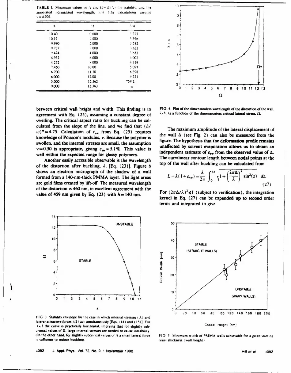
TABLE 1. Minimum ýalues or % and =! I A for stabilhtv. and the T"
associated normalized wavelength. (. the calculations assumel 0. 50).
9
A 11 h
10.40 :) 000 277 -
10.19 ' 000 1 399.990 :.00 3 582 6-).737 ,000 3 6231).474 4000 "553{.932 o0l00 4.002S272 000 4319 47.450 io.O0 5.0976.700 !1 30 o.3986.000 12.08 9.7215.000 12.362 759.2 2"0.000 12.363 0 2 3 4 5 6 7 8 9 10 11 12 13
between critical wall height and width. This finding is in FIG. 4. Plot of the dimensionless wavelength of the distortion of the wall.
agreement with Eq. (25), assuming a constant degree of A/h. as a function of the dimensionless critical lateral surs fl.
swelling. The cntical aspect ratio for buckling can be cal-culated from the slope of the line, and we find that (hi The maximum amplitude of the lateral displacement ofw)*=4.75. Calculation of e,, from Eq. (25) requires the wall I (see Fig. 2) can also be measured from theknowledge of Poisson's modulus. v. Because the polymer is figure. The hypothesis that the deformation profie remainsswollen. and the internal stresses are small, the assumption unaffected by solvent evaporation allows us to obtain anv=0.50 is appropriate, giving e,.,=5.1%. This value Is independent estimate of s from the observed value of A.well within the expected range for glassy polymers. needn siaeo s rmteomre au fA
Al hnother easilyaccessiblge fobervglablesisy pomer. wThe curvilinear contour length between nodal points at theA nother easily accessible observable is the w avelen gth to of he w l at r bu ki g c n e c l u a ed r mof the distortion after buckling, A, [Eq. (23)1. Figure 6 top of the wall after buckling can be calculated fromshows an electron micrograph of the shadow of a wall A 2 2i7r& )2 2 2Zrformed from a 140-nm-thick PMMA layer. The light areas L =A( I +E,.) = - I + •---) sin2z) dz.are gold films created by lift-off. The measured wavelength 0 (27)of the distortion is 460 nm, in excellent agrecment with thevalu of459nm ive byEq.(23 wih h140nm.For (2irA/A) 2 < (subject to verification), the integration
kernel in Eq. (27) can be expanded up to second orderterms and integrated to give
14
___1,2_ UNSTABLE 50.
T10. 40
STABLE
8 (STRAIGHT WALLS)
E 306 STABLE
4V
20
2UUNSTABLE
00 3 4 5 6 7 8 9 1011 (WAVY WALLS)
A
0 ,2 .0 60 80 *00 120 140 160 180 200FIG. 3 Stability envelope for the case in which internal stresses I A) andlateral attractive forces (11) act simultaneously (FEqs. 1 14) and 1 15)1 For%%.5 the curve is practically honizontal. implying that for slightly sub- Crtcal Height (nmfcntical values of fl. large internal stresses are needed to cause instabilityon the other hand. for slightly subcnu.cal values of A a small lateral force FIG 5 Minimum width of PMMA wails achievable for a given sianrne!s sufficient to induce buckling. resist thickness w wall height)
4092 J. Appi. Phiys.. Vol. 72. No. 9. 1 Novertrie 1992 Hill et at 4092
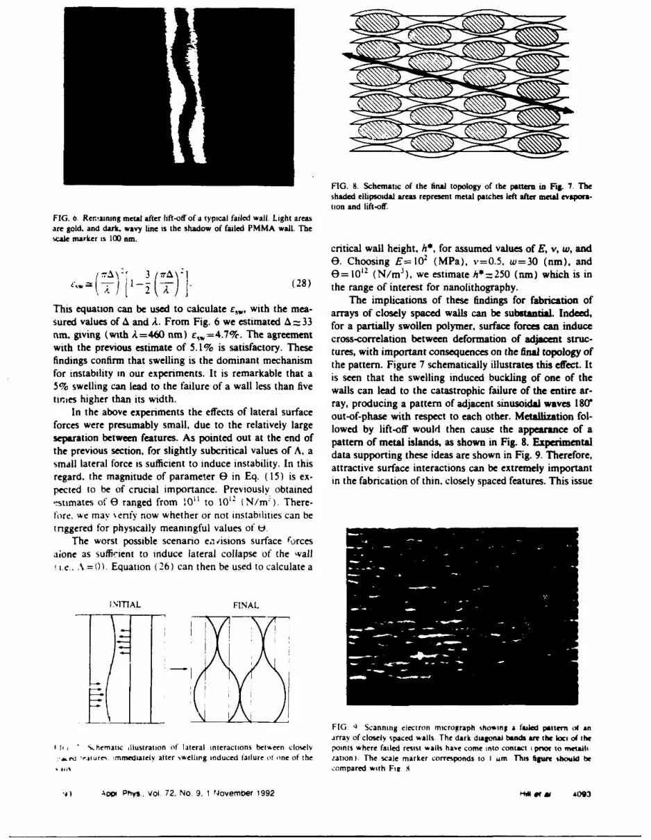
FIG. 8. Schematic of the final topology of the pattern n Fig. 7. Theshaded ellipsoidal areas represent metal patches left after metal evapora-tion and lift-off.
FIG. 6. Remaining metal after lift-off of a typical failed wall. Light areasare gold. and dark, wavy line is the shadow of failed PMMA wall. Thescale marker is 100 nm.
critical wall height, h*, for assumed values of E, v, w, and0. Choosing E= 102 (MPa), v=0.5, w=30 (nm), and
,A 3 (_A)] = 1012 (N/r 3 ), we estimate h*=250 (rum) which is in" A -(28) the range of interest for nanolithography.
The implications of these findings for fabrication ofThis equation can be used to calculate e with the mea- arrays of closely spaced walls can be substantial Indeed,sured values of A and A. From Fig. 6 we estimated A= 33 for a partially swollen polymer, surface forces can inducenm, giving (with A.=460 nm) E,.=4.7%. The agreement cross-correlation between deformation of adjacent struc-with the previous estimate of 5. 1% is satisfactory. These tures, with important consequences on the final topology offindings confirm that swelling is the dominant mechanism the pattern. Figure 7 schematically illustrates this effect. Itfor instability in our experiments. It is remarkable that a is seen that the swelling induced buckling of one of the5% swelling can lead to the failure of a wall less than five walls can lead to the catastrophic failure of the entire ar-tirnes higher than its width. ray, producing a pattern of adjacent sinusoidal waves 1880
In the above experiments the effects of lateral surface out-of-phase with respect to each other. Metallization fol-forces were presumably small, due to the relatively large lowed by lift-off would then cause the appearance of aseparation between features. As pointed out at the end of pattern of metal islands, as shown in Fig. 8. Experimentalthe previous section, for slightly subcritical values of A, a data supporting these ideas are shown in Fig. 9. Therefore,small lateral force is sufficient to induce instability. In this attractive surface interactions can be extremely importantregard, the magnitude of parameter E in Eq. (15) is ex- in the fabrication of thin, closely spaced features. This issuepected to be of crucial importance. Previously obtained.stimates of E ranged from II to 1012 (N/mr). There-
Core. we may Nenfy now whether or not instabilities can betriggered for physically meaningful values of H.
The worst possible scenario eavisions surface forcesaione as suffi-ient to induce lateral collapse of the wall!e...\ =0) Equation 26) can then be used to calculate a
INITIAL FINAL
-J -I
FIG 1) Scanning electron micrograph showing a failed pattern of anarray of closely spaced walls. The dark diagonal bands are the loci of the
, .hemwtic illustration (if lateral interactions between closely points where failed resist walls have come into contatt tprior to metalti:.,n• atturr' :mmediately after swellirg induced failure ot one of the tation). The scale marker corresponds to I um This figure should beIA ,,,compared with Fill 4
.'# Aopi Phys.. Vol. 72. No. 9. 1 November 1992 HO or a 03

is especially crucial when dealing with marginally poor &ulated the stability envetope and wavelength of the distor-solvents, as is the case for most post-development. nnsing ton for the general case in which internal swelling stressessolutions. and lateral surface torces act simultaneously. We also
As a final note on the modeling of wail stabihty. the -,howed experimental evidence that supports our predic-following points must be considered. First. in the theoret- tions, thus demonstrating the existence and seventy ofical treatment we have ignored the effect of hydrodynamic "uch instabilities in nanolithography. In the limiting caseforces which, at least in principle, could also be invoked as of small surface forces. preoictions and data agreed quan-a source of instability (e.g.. agitation during development ). titatively. Order-of-magnitude calculations of the strengthIn fact. such effects are unimportant within the context of of the lateral interactions between polymer walls (based onthe stability problem. since upon cessation of flow a hypo- experimental surface force data) confirmed that lateral at-thetically deformed structure would always "spnng back" tractive forces can substantially enhance the action ofto its most stable configuration (as dictated by the equilib- swelling stresses, leading eventually to failure. Practicalrium criteria derived previously). Additionally, hydrody- implications of these instabilities in the fabrication of ar-namic effects cannot explain the correlation between defor- rays of closely spaced polymer walls were discussed. For-mation of adjacent structures observed in Fig. 9. Second, mulation of developers that maximize contrast, but mini-our simplified analysis assumes that the walls are: (I) mize swelling and attractive interfacial forces, is thusstrongly anchored at the bottom and (2) of constant relevant to attempts to achieve higher resolution in nano-width. The validity of the first assumption is easily inferred structure fabrication.
from the experiments, since floppy, weakly anchored wallswould be incapable of retaining a deformed configuration ACKNOWLEDGMENTSof high strain energy such as the one shown in Fig. 6. Inregards to the second assumption, we know that it cannot We would like to thank D. T. Leighton for helpfulbe entirely accurate, since undercutting inevitably leads to discussions and S. Subramaniam for help in sample prep-walls of decreasing thickness from top to bottom. A full aration. This research was supported in part by IBM,analysis of this effect goes beyond the scope of the present AFOSR, ONR, and the University of Notre Dame. D. A.work, but simple qualitative arguments in support of our H. gratefully acknowledges partial support by the Donorsapproximation can be offered for the case of mildly ta- of The Petroleum Research Fund, administered by thepered, strongly anchored walls in the swelling dominated American Chemical Society.regime (i.e., fl<A). Indeed, due to the anchoring bound-ary condition, the deformation at the bottom of the wall is D. R. Alice, S. Y. Chou. J. S. Hams. Jr.. and IL F. W. Pease, J. Vac.
small [see Eq. (16)]. Therefore, as a result of buckling, Sci. Technol. B 7, 2015 (1989).regions of the wall closer to the surface experience neither 'J. C. Wu, M. N. Wyboume. W. YindeepoL A. Weisthaar, and S. M.an appreciable release of strain energy nor a sizable de- Goodnick, Appi. Phys. Lett. 59. 102 (1991).
eof surface free energy. In other words, the bottom IS. Y. Chou, Y. Liu. and P. B. Fischer. IEDM 91, 745 (1991).crease o r erm 'J. 1. Goldstein. in Introduction to Analytical Electmn Microtopy, editedportion of the wall contributes negligibly to the onset of by J. J. Hren, J. L Goldstein. and D. C. Joy (Plenum. New York.instability, since its contribution to the overall energy bal- 1979), p. 0t1.ance is small. The relevant wall width. w. controlling the G' Owen. Repts. Prog. Phys. 48. N95 (1985).onset of the instability [i.e., the value to be used in Eqs. 'A Wezil, in The Physics and Fabrication of Microstnuctures and MV-
crodevwces. edited by M J Kelly Ind C. Wetsbuch (Springer. New14) and (22)] should then be closest in value to that at York. 1986). p 58
the top, free end. This argument is also consistent with the W M. Moreau. Semiconductor Lithograpy (Plenum. New York.fact that, for fl<cA. the wavelength of the distortion, A [Eq. 1988). chap. 10.
G. Park and K. Ueberreiter. in Diffusion an Polymet,. edited by J Crank(23)), is independent of w. and G. Park (Academic. New York. 1968). pp. 140-162. 219-257
"I N Israelachvila and D Tabor. Proc R. Soc. London Set" A 331. 19SUMMARY AND CONCLUSIONS (1,72)
'S S Patel and M Tirrell. Ann Rev Phvs Chem 40, 597 (19891Upon exposure to suitable solvents such as common G H Bernstein. D A Hill. and %k P Liu. J Appl. Phy 71. 4O06
developing and rinsing solutions, nanofabncated polymeric (1992)walls may become unstable as a result of two effects: ( I ) H J Taunton. C Toprakcioptu. L I Fetters. and J Klein. Macromol-
" ecules 23. ','! 1 IIJI)lswelling and (2) lateral surface forces between adjacent S P Timoshenko and J M ,ere rlweorv of Elastt¢ Stabihty. 2nd ed
,,tructures. By performing a linear stability analysis we cal- McGraw.Hill. %ew Nork. ;h 3
AM P"y wooa * 2 %o 4'~ Nova."io * 992 "so f a 4004

Best Avaiable Copy
Supmiattices and Microstructures, Vol. 12Z No. 1. 7992 123
FEATURES OF QUANTUM MAGNETOTRANSPORT ANDELECTROMIGRATION IN MESOSCOPIC SYSTEMS
S. Bandvopadhvay, S. Chaudburi and B. DasDepartment of Electrical Engineering
University of Notre Dame
M. CahayDepatmen ofElectrical and Computer Engineering
University ofCincinnatiCincinnati. Oho45221
(Received 4 August 1992)
hae cacltr hiwo-dimensional pta distributions of several urarisport variablessuc asthecun desit. cmerconertraton.chemical porenndal. sarue-charge electric field.
resdua mstivtydiple otetia ad cectomiratonforces in disordered meaoscopic sauc-tut v~we toaritrrymagmmfields. Thnflyquarmaim mechanica calculatiou shad
new lih nsc anttasotphetinoena as dhe integer quaantum Hail effect. tie formationrof agnticboud sate. mgneicresponse of currnt vortices caused by quaintum interferenicebetwen satteem te num ofresidual resistivity dipoles in phase coherent traisport. die dif-Wene btwen mjorty-andmirnony-camrer mobilities in dhe quantumi mechanical regime.dieeletio wid frceaddirctforce of elecuuutigration in a mesoscopac system. and a
vait of ondian 46556ena
Introduction Thi p is orgmaned as follows. In die next section. wedescribe dhe theoiry (or caklcalaizig spatial distributions of trman-
The patal mburm o trr~prt anabes myc asthe pon variables in memsocope structures. We then presPe- reaultecu.nudnit.w ae concentratio. chemical pieu. ed- dealing with the two-dimeauaorul spatial distribution of die cur-
va esuiviy 4ok etl c.) ane importan in uldiemnldaig rent density in a dsordered smnictre at various magnetic fields.maryqumi uWoOmmomna' in mesouCWpa aaCture The current ditsunbuuion; show a number of dranmatc effectmW lm kcuml - ffocum1- In aLhis papr, we pmemu a such mcurrent crowding neaw an attractive impurity. currenmocigeost:cakli m o sch spatial distribistioua in a quas desow around a repulsive impurity. dhe formation of edge seLumdimamma Arhmco"Uwamag localixed impurites and with perfect irmumuvity as die onues of dic insiger quamimsmocodw wmmymagmucfieldii. The cacualaucunsm - by Hagl 4ecz camalamag cuimi pownen antied an mnipuwiy due6
4imma-ricow ar = uMandraik Schlvadwipr erause.. asearem of die hientamau of nW41maci boundi tarn. fmormatido ymi. w m*as Wmdu die nmm fa 01 W" o dvrum veraa (mn ft aboace of any mawmuc fiel) as
diftno 1VW of fmmmi 00 WW poun mumim te . a menk of qom ume- ft ma betwomi waves reflected fromdowa gime Oafict.cwinm vouuat fouunaimi. ac.). vatim 6mpurities ma upie. the quaric*Uing of such vnm
mW dy ai da lift ana" 0 i I cu. pasiacukely by a magnrrc kied, aind so on.Pc Th se uksu and adieu anethewW Amadthed~ctforce ont W ato A Caam le~cti- acesmnpented by Ohe carmepondidng modulations in the carrier
,omri ibElectiompgguuon is an epuci~lva imponant .numo peodil consrd by cunrem flow Fmom dime pro-01- , tnn mw m -d --amiam nmanamc tpies. Fim am can ciceuly -n die bwIdting up of an cxcia @Itctim
rwGv nt "o 01nof cainuI camimaplmc device canr aro mi an asnsctivit scanewe and a defctH amusedfu'rset n i domi crwu.twai in aOwa it causes a virdm mm oin WeiscmUusua 0'inea of tm 'lew..
m~ne iiminwhb d dv dms u~ clao amc withdrerm otr Ahu. emiteacu m d I mdam ps-WA 11111111111 1/14ý tv it animptn oE hed-im t is suraeave or repulgve whim
07*6403S192/S01 23 * 10 ON 00/0 V 1 "2 Acadirer:a Pmw UnLmund
124 Superlattices and Microstructures, Vol. 12. No. 1, 1992
a magnetic bound state fornms. ehCse accumulations and dcpie-tions lead to inhomogcneciies in the charge distribution which. 0 N,in Dim. lead to inhomogenetucs in the electric field within thesanple. Such irihomogeneities have a profound effect on thedriving forces of electromigrauton acting on an impurity locatedinside the sample.
In addition to the spatial distnbutions of the current densityand carrier conccmration modulation, we also show the spatal !
dis-tnbuuon of the chemical potcitial inside a sample. In the * Fig. I: A quasi one-dimensional structure containing a ran-absencc of any magrietic field, the chemical potcntial protiles dom distribution of clastic scantcrers. The structure is thinshow very different features depending on whethcr the scatter- enough in the z-direction to allow the occupaton of only onecrs ae atutacijve or repulsive. When a magneuc field is applied, transverse subband in that direction. The magnetic field is in'he chemical potential profiles for both attractive and repulsive the z-direction.scatterers change dramatically. At high enough magnetic fields,Jhe edges of the structure (along the direction of current flow) transverse subband can be occupied in the zdimctimt i.e. thebecome surikingly smooth equipotential surfaces. This happens confinement is complete in the z-direction). Howe'tcr. multipleeven when t.e potential at the center of the structure is exhibit- t-anserse subbands may beL occupied in the y-direwi m.ing chaotic behavior. As a result, the longitudinal resistance The Schrdinger equation describing this sys'n under ameasured by voltage probes attached to the edges of the struc- z-directed magnetic field isiure will always mad precisely zero (in a four-probe measure-ment). This is a clear dcmonstration of the quantum Hall effect. (,_ e,+ =(Almo, we find that the chemical potential difference between c"the two edges of the structure (i.e. the Hall voltage drop) iseacy equal to the chmica poential drop between he wo where f is the momentum operator, m" is an isotropic effective
ceacts of the structure when a single spin degenerate subband miss. A is the magnetic vector potential. e.(z.y) is the two-
is occupied. Since the quantum mechanical transmission pro- dinsiora wavefunction, and the potntial energy V consistsablity th-ough the structure is exactly unity when this happens. of two i~rsit means that the Hall resistance is precisely quantized to h/2e(
h'ijch is an unequivocal demonstration of the integer quantum
Hall effect. It should be noted that these results pertaining to The first term gives the effect of the -onfining potential in the:he integer quantum Hall effect are found from a rigorous mi- y-direction and the second term is due to impurities. We as-,oscopic calculation and do not invoke any phenornenological sume hardwall boundary conditions in the y-direction and delta
.. Sun't:. potentials for the impurities so that we haveFrom the electrostatic potential proile. we have calculated
the electnc field distribution in the structure. The field showssigr••icant inhoanogeneities which havc a profound influence on Y,,,)"z ) - - t, i( i - M, ) •3)
elecsromigrauon. Electromigration is caused by forces actingon charged impuntes (ions) wifthn the structure which tend to where s is the total number of impurities in the structure andcause ion motion. Such motion can drastically alter the behavior the summation extends over all the impurities. The position ofof the structure in the phase coherent regime. lead to I/f noise, the ith impurity is denoted by * x, y,). In all our calculations,and. in the extreme case. physically disrupt the structure leading we neglect effects associated with the spin of the election.to total device failure. The two main forces of elcctromigration The confining potential in the v-direction and the z-diectedam the "wind force" caused by collisions with elcctrors flowing magnetic field give rise to a set of hybrid magnetolectric sub-past the ion and the "direct force" due to the electrc field acting bands in the y-direction. Each such subband corresponds to aon the ion. We have calculated the spauai distribution of the so- mode or a transport channel. Calling o,(y) the y-eomponpeitcalled residual resistivity dipole potenual which has a profound of the wavefunction in the ruth magnetoclectric subbmd, weeffect on the "wind force". In addition, the directions of both can write the total wavefuiction WE,..,(Z.Y) for an electronthe "wind force" and the "direct forme" at various ion locations injected fromn the left contact with the Fermi energy E4 into theand at varying magnetic field have also been calculated. To mth magnetoelecuic subband asour knwlcdge these arm the first calculations of the effects of Amagnetic field on electromigration forces in mesoscopic samples ., A,,,( z ),rp(ii4z )¢,(i)in the quantum coherenoe regime. VE.,PM(ZY) = E
Sp=i vl1
Theory + [D. (,,(4)
We consider a quasi one-dimens•rial structure as shown in where L is the length of the structure, and k. and vf am theFigu= 1. The thickness is small enough that only a single x-dimcted wavevector and x-directed group velocitycormrspond.

Superattices and Microstructures. Vol. 12. No. 1. 19,92 125
the forces of clcctromigration. The recipes for calculating these" .... quantities from the wavefuncuon are descnbed in the foWowing
'd r""i , EC pagraphs""�/ 'I . Spatial distribution of the current: In linear rexponse
S .. - , ,transport and at low temperatures. only electrons with the Fermi'4 p '• ' -'- " ' + '• • • ' ,energy ca" r a net current. Therefore. fth tw o-dil c mn= XX
"I I ' wavefunctionn y( ) of Fermi electrons in the mth magneto-• ',l // ,' felectric subband allows us to calculate the contribution of that
Sto •. /• .• • / ' . subband to the two-dimensional current density ,(z,i,).S.7 / :
2m I
IlThe total current density is then found by vectonally adding theSo 4 -0 3 -0.2 - 0. 2 2 1 0 2 03 0 4 contifbutions from all occupied subbands (propagating modes).
4 (11'nfi U'
= Fig. 2: The encrgy-dispersion relations for the hybrid mag- (Z'Y) .('-) (6)newLtuic subbands in a 2(000 X wide structure at a magneticflux density of 1.5 TeSIL The solid curves am the result of The above xprmssion provides the curent density at every co-an excx numerical calculation and the broken curves are those ordinate point (z, p). Nowe tha. in calculating the total curtobtaned from the application of Bohr-Sommerfeld quantizaton density by summing over subbands. no weighting by the densityrile. of states is necessary in the snmmation since the wavefunctioni
have been normalized by the square root of vt-tocity which takescame of the density of stows factor. The above equation givesing b) the Fermi energy in the nth subband (see Fig. 2). These the two-dimcmonal spau,1 distrbutn of the currnt density
quanvities are found from the dispersion relation of the hybrid o amagnetoelecric subbands. The method for finding the disper- ~centraon and configuration of scatterers and for any magneticsion relations. as well as the wave'uncuons o,(y) in the nth field.magnetoelectric subband. has been described in reference 4 andwitU noA be repeated herm. Finally, the subscript -p in Equation Carrier concentration change due to transport andi4) indicates that the quantity corresponds to a wavefuncuon its spatial distribution: To calculate the change in the car-with an oppositely directed velocity as compared to the one ncr concentration caused by a curre, we follow the method ofwith a subscript p. QCu and SorbdeHo. At low enough tempratuems. the deviation
In Equation (4). the summation over p (subbamt index) ex- of the sniclassical election distribution function fron the equi-tends over both occupied and unoccupied subbands (i.e. both liblium value in the mth subband (as caused by a small appliedpropagating and evanescert modcs). It is important to include electric field C driving the current) is given byenough evanescent modes in the summation so that the com-puited waveunction does not depend on the nurmber of terms AJf 1(E) -er(E,m)C(E- CF) (7)(M) in the summiaioe. Even though the evascev modes do h - is a contanelxai time dcribing a ufone beck-not carry cuffner, they have very sigrificara efFects on all tram- guoud scanting due to all elastic collisions and v( C, m) is sheport varisatbs and especially their spatial distrbtiom'. group velocity corresponding to electron energy E is the mth
When the wavefunction is wrinten in the form of Equaton subtand.(4). (i.e. each mode indexed by +p is normalized by the square The chage in the cartier concnration due to the cunuw ismat of the corrsponding group velocity), all propagating modes then given byat the Fermi energy carry the same current. This is conwith the well-known cancellation of the velocity and density of U
in quasi one-dimemnonal sitrutures which causes every 6n.(z.y) : JdENt•..u E)A/.(E)Its.,(zy)I2 , (8)mode to carry the same current. To find the total wavefuncton 'g iven by Equatm (4), we now only have to "duse the coeffi-cieuns byq,(z) and B,,(w). Thes ave found from a scatterng where Nl.,,(E) is the one-dimensional density of states in
matrix method that has been described in the first two citape the rth magnetoelectric subbard (die pnscnpto for cacu.in IFer-nce I. Once the wavcfunction has been evaluated, we lating this was provided in refetrtrce 4). M' is the total nuambercam scalt all quantities of interest such as the spatial dis- of propagating modes or occupied subbarad. and *£,,.. is thetuiclia of the curren, carrier concentration profiles. residual wavetnction of Fermi elections in the mth magnetelectric sub-resisivity dipole potential, chemical potential. electric field, and band. This wavefunction is not exactly the same as that

~28Superlatmces and MiCroStructures. Vol. 12, No. 1, 1992
cy Equation (4); tile oniy difference is that there should be no where the night hand side is the rate of loss of electron momen.I-omializ~aton of the vanous modes; bv the square-roor of veloc' turn due to COllisions With the ioOf. It can be shown- from aity in calculating "FE.,. T1herefore, if we use Equation 14) f3r rigorous semiclassical treatment based on the Boltzmann trans-the Wavefunction. then 6 i iy should be be wntten as port equation that the right hand side is -J10141/iir where n is
the volume concentration and Y7 is a semiclassical mobility asso-= -~ ciated wit scattering by the ion. In thc linear response regime.
the bov qunutyis lsoequal to the negative of the spatialgradient of the chemical potential (quasi Fermi level). T7here-
-, hecm v is now given by equaiion (4). Thbe above equation gives fore, the wind force an an ion located at coordinate (zo, yo) canithe spauall distribution of the change in the carrier concentration be~ fon directly from the chemical potential profile around theas a consequeric of transport. ion.
Spatial distribution of the residual resistivity dipole-potential: When an imnpurity is introduced in a solid, the Pý~.,Wt 0. YO) = -tW(Zo.YO) .(12)
resistance increases. Th-is increase is associated ;with the for ma- where ui the chemical potential.tionof "rsidul rsisrv~v diole amnd he ipunv tchT~he above calculation of the winid force relies on the ba-
.anses purely from (he interaction of electrons with the impurity sic theory of reference 5 which does not distinguish betweeniscaaerinng). Landauerý has pointed out that the residual re- crystal momentum and reall momentum in a solid. Mome sophis-sistivity dipole potential is an Important source of electric field ticated thocli requirt knowledge of the exact: shape of fthinhoinogneitics in a sample and affects the so calld wid ion potential and also the exm spatial distribution of the chargeforce- of electromigration The wi-d force is the force that act pile up (or charge deficiency in the case of repulsive scastereri)on an trnpunry owing to collisions with electrons during currnt around ions. These sophisticated theories could actually benefittranspoit. from OWr quantum mechanical calculations of the change in the
To calculate the spatial distribution of the residual resistivity chrg density around the ions catused by current flow (describeddipole potential, we follow Cihu and Sor`bello2. According to previousy in this section). A fully quantum mechanical, self-these authors. the electrostatic potential arising fro hn n h consistent and rigoros calculation of the wind force_ startinginduced screening Charge which attempts to locally neutralize frown fth Schr6dinger-Poisson equations is reserved for A future6n, is the residual resistivity dipole potential. %Within a Fermi- ulciinThomas model. seif-consisgent screening gives this potential as
I The "direct force" of electromigration: T7he direct forceon an ion in a solid subjected to an electric field is the electro-
e static force gvnb
EF 10)fd~re, Zef(13)
,he,.c tn., is u_. fro1m fth mith magneto- where Z is the effective valency of the ion arid tis the localelectric stibobii electric field at the ion site.
From the above equation. we can readily obtain the spa- Boveu n Friedels claimed that the diffemrene in thetiaj disflitxion of the residual resistivity dipole potential. 71h charg of an interstitial ion from the background will be conm-residual resistivity dipole field is the spatial gradienit of this pn- pletely screened by the elections so that the local electric fieldtentlal. in contras to the claim of referenice 3. thi fil oe o and hence: the direct forcie on such an ion will be exactly zero.have to be always directed along the direction of current flow. Gutadcowres 0 onlediasmlrvinhtteespecialy when quantum confinementr (quantum size effect) an direc force on a migrafing ion in the saddle point position isquantum irwerfererice (coherent effect) ame important. exactly zero.The -wind force" of eleetromigration: The wind force is It was correctly pointed out by Das and Peierls' t and alsothe fo~crm tan ion or impurity ina solidcexpencrice~sowing o Lardauer13that Bosvieux and Fredel could not be correct sincean "election wind- flowing pant it during curren transport. This fthir conclusion leads to inconsistencies. For instance, if anelection wind imparts a force on the ion because the electrons interstitial proton were completely screened and the loca fieldcollide with the ion and transfiers momcnaimu to the ion. The is zero. then it should be also true of electrons and consequentlywind fo=t causes electronigruion (motion of ions or impuni- a metal should have no electrical conductivity.tie) wtids has several effects in mesoscopic structures such as The correct equation to use for the direct force is Equationalteratiormof sample conductance Ilf noise. and electrical failure (13). but the electric field in that equation is not the space-cause by physical disruption of fth sample at critical regions. averaged electric field as assumed by Huntington' and by Lo~u
To calculate the wind for=eon an ion, we follow h wr eL &L14. Itwas stressed by L*ndauer that the field is afleted byof Fiks and Huntington and Grown5 who invoke Newton's law. the "charge density modulation" around an impurity that occursThe wind fomc is given by during current flow. Therefore the field must be calculated self-
consistently by solving fth Poisson and Schiddinger equation.L /dp\ 1) in the linear rspons regime. this field can be obtained without
\dt/~amuch difficulty as described below.
Superla/tices and Microsituctures, Vol. 12, No. 1, 1992 127
spatial distribution of the chemical potential andelectric field: Any nct charge distnbuton p(-r, y gives riseto an electrostatic potcntial I i z. xy and an electric licld 4.'(Xz. y)which are related to the charge distmbution through the Poissonequation..
, • .z• v1(. .. . .............
It was shown by Ultikert 5 and Entin-Wohlman ct. al.1" :that in the linear response regime. and in situations where thespatial variation in the potential V"z. y) is smooth on the scaleof the screening length (i.e. the screening is very strong), thepotential is given by
•,,",• .(a)• •'t.,(r Y!? W I L'.2.,,( ýt'111,112
where /t and P2 are the chemical potentials (Fermi energy) in -... .. .. .. .. .. .. .
the two contacts of the structure under investigation. i - - - --.------------the wavefunction of electrons injected from the left contact insubband m with energy it, and e,7, is the wavefunction of clec-truns injected in mode m with energy P2 from the right contact.--It was pointed out by Entin-Wohlman ct. alI. that eV(z.y)is also what is actually measured at a chemical potential probe - -- - - -
so that it is also the chemical potential. In other words, in this -
regime. eV M p.Once the electrostatic (or chemical) potential is determined.
the corresponding electric ficld is found simply from K :...:... .. .. .. .. ..
g~~z~~yjz I 1(zy= -1Vji(z' Y). 16(b
This is the elcctnc field that should enter Equation (13) for the A g. 3: The spatial distribution of the cunt densitydirect force in the linear response regime. Note that this means in a 800Th longialdis 000ton wide c trr e itthat the wind force and the direct force are equal in this regime tabsen of an d The Fi energy isthe absence of any magnetic field. The Fermi energy is 2.054if the valency Z of the ion is unity.In the venceZofthe ion, is unity. rul cmeV. (a). Current crowding around an attractive impurity. (b).
In the next section. we present results dcaling with the current detour around a repulsive impurity.spatial distribution of the current, carrier concentration changecaused by the current. the chemical potential profile, the resid-ual resistivity dipole potential, and the wind force and directforce on impurities in a prototypical GaAs quantum wire con-taining elastic delta scattrers. We consider both attractive andr e p u l s i v e s c a t t e r e r s a n d s h o w s o m e t y p i c a l e x a m p l e s o f h o w t h e . . . . . . . . . . . . . . . . . . . . . . . . . .spatial patterns respond to an external magnetic field.
Results ..................
Spatial distribution of the current around a single Lscatterer - local effects: We consider a GaAs wire whichis 800 A long and 1000 A wide. The Fermi energy is, 2.054
meV corresponding to an electron concentration of 3.85x 100/m.For this low concentration. only one subband is occupied inboth transverse directions so that transport is strictly single-chanmeded.
In Figures 3(s) and 3(b). we show the current profiles around Fig. 4: The spatial distribution of the cumnt densitya single attractive and repulsive scatterer respectively in the ab- J y.1 6 j(z, ) in the structure of Fig. 3(a) when a magnetic fltxsene of any magnetic field. In the case of an attractive scatter•r, density of 2.18 Tesla is applied. The current flows along the topthe current is drawn closer to the scattrer, whereas for a repul. edge indicative of the form ation of "edge statU". This siationsive scaterer, the current detours around the scatterer. This corresponds to the onset of the ineger qwummm Hall ct.
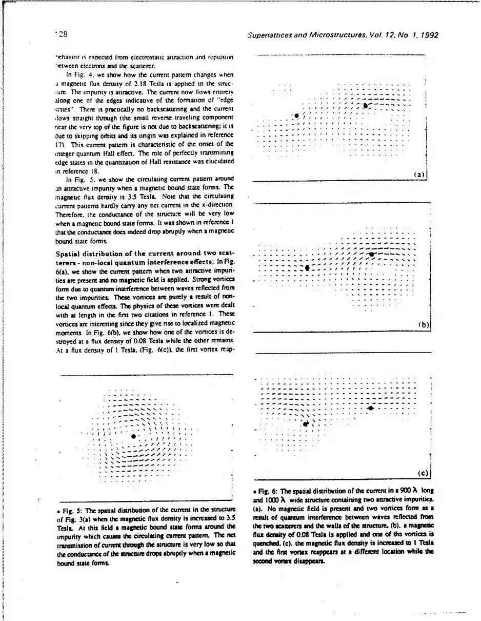
SISI Super/a wces and Microstructures, Vol. 12. No 1. 1992
�ior is expected from clectrosiatic attraction and rcpuhsion
�.tween elecuTma and the scatterer.
in Fig. 4, we show how the current pattcm changes whena magnetic flux density at 2.18 Tesla is applied to the struc-�ure. The impuntv is attractive. The current now Ilows entirely - - ------
along one of the edges indicative at the formation of 'edge '' - �-'
�turs'. There is practically no backscattenng and the current '' ' ' / ' / - - .. .. ..
lows straight through (the small reverse traveling component -
near the very top of the figure is noc due to backacatteillig; it �s- .. A
due to skipping orbits and its ongin was explained in reference . . . - �-. -................................................
17'). This current pastern is characteristic at the onset of the . . .
integer quantum Hall effect. 'The role at perfectly transmitting
in reterence 18.edge states in the quantization of Hall resistance was elucidated
In Fig. 5. we show the circulating current pattern around (a)Jan attractive impurity when a magnetic bound state forms. Themagnetic flux density is 3.5 TesIs. Note that the circulating�urrent pattems hardly carry any net current in the x.direction.Therefore, the conductance of the stmctue will be very lowwhen a magnetic bound state forms. It was shown in reference Ithat the conductance does indeed drop abiupily when a magneticbound state forms.
Spatial distribution of the current around two scat-......................--- - - - � - -------------------------------------- ,
terers- non-local quantum anterterence effects: In Fig. � '.'.'
6(a). we show the current pattern when two attractive rnpun- - - - ' ' ' '- III....,�
ties are present and no magnetic field is applied. Strong vortices -.................
form due to quaniwn interference between waves reflected fromthe two impunties. These vortices are purely a result of non-local quantum effects. The physics of these vortices were dealt .
with at length in the first two citations in reference I. These(b)�
vortices are interesting since they give rise to localized magneticmoments. In Fig. 6(b). we show how one of the vortices is de-stroyed at a flux density of 0.08 Tesla while the other remains.At a flux density of I Tesla. (Fig. 6(c)). the first vortex reap- _______________________________________________________
----------------------------------------------
---------------------------------------------
- . -------.- - . - . ----- ��s............- ------. '' - -.......--------------
- '��'-%\"�..........
* �.,,I � -
I J I ''� ' ,0*9�' .
I.. .
-"''''� - .
- . S '*= -- - -
____________________________________________ (C)
eFig. 6: ThespaoaldistributionofthecurrentitIa900)� longand 1000 )� wide stiucture containing two aursetive impurities.
* Fig. 5: The spatial dntnbution of the current in the structure (a). No magnetic field is present and two vortices form as a
of Fig. 3(a) when the magnetic flux density is increased to 3.5 result of quuuwn interference between waves reflected fromTesia. At this field a magnetic bound state forms awsmd the the two scaucren and the walls of the atnictuwe. (la). a magneticimpunty which causes the cnvulatzng current pattern. The net flux density of 0.08 Teals Is applied and one of the vortices is
transmission of Current through the structure is very low so that quenched. (c). the magnetic flux density is increased m I Tealsthe conductance of the smactum drops abrupdy when a magnetic and the firat vortex reappears at a different location while thebota'd state forms. seound vor�x disappears.
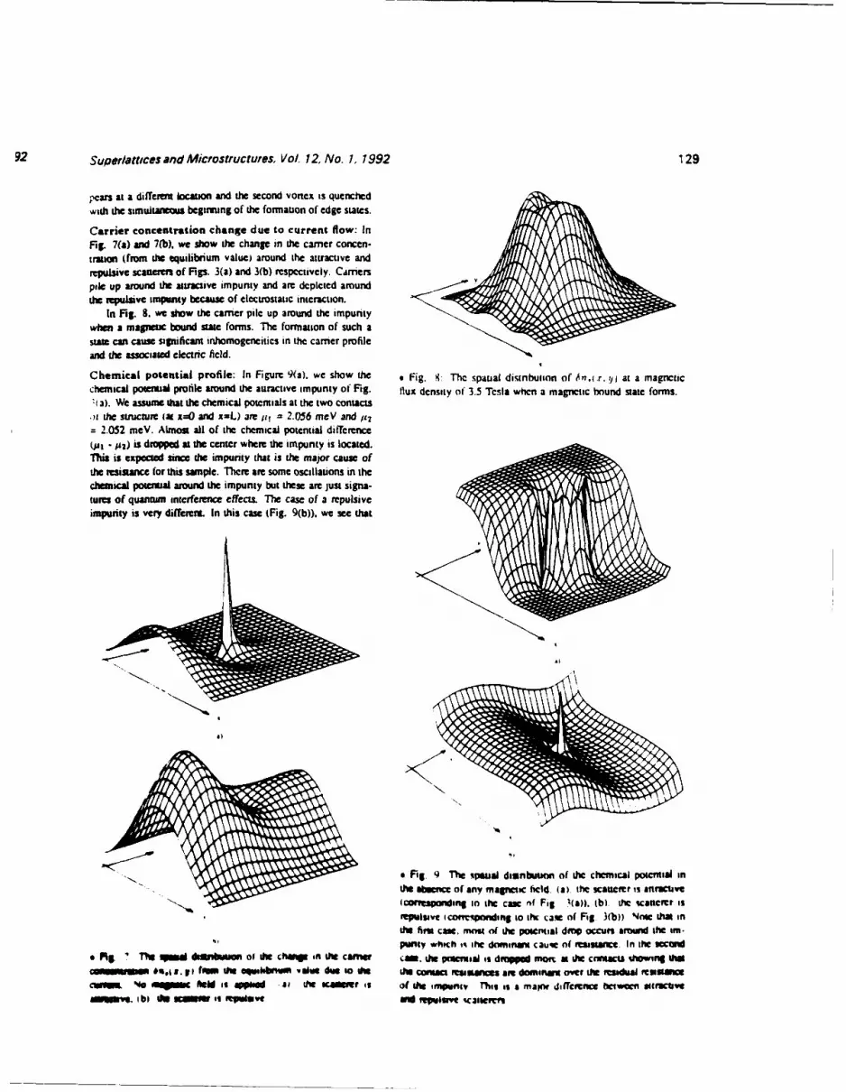
92 Supelatuces and Micaosfrucfures. Vol. 12. No. 1, 7992 129
pcan at a different location maid the second vortex is quenchedwith the smunuitneous beginning of the formation of edge states.
Carrier concentration change due to current flow: InFig. 7(a) and 7(b). we show the change in the carrier concen-traiton (from the equilibrium value) around the attractive andrepuilsive: scantePut of Figs. 3(a) and 3(b) respectively. Cdrncrs9iLe up around the attractive impunity and are depicted aroundthe repulsive impamty becaue of electrostatic interaction.
In Fig. S. we show the earner pile up around the impuritywhen a magnetic bound state forms. The formation of such astate can cause significant inhomogeneitics in the earner profileand dhe associated electric field.
Chemical potential profile: In Figure 9(a). we show the Fig. 9: Thc spautia di-tnhution of i6n,.r. 9 1 at a magneticchemical potential profile around the attractive impurity 0f Fig. flux density of 3.5 Tcsla when a magnectic hound state forms.
a(). We assume that the chemical potentials at the two contactsot the stucucnre (at x=O and x=L) are it = 2.056 meY and ft,= 2.052 meV. Almost all of the chemical potential diffecrence1stl - y2) is dropped at the center where the impunity is located.This is expected since the impurity that is the major cause ofthe resistanc for this sample. There are some osctllauions in thechemical poew"a around the impurity but these are just signa-turn of quantum interference effects. The case of a repulsiveimpurity is very different. In this case (Fig. 9(b)). we see that
Fig 9 The spenual distribtion of the chemical potential inthe I PercP of any magnectic field. (a). the scatctere is attractive(corresponding in the case mf Fig I(a). (b). the wscaterr isrepulsive iconvspondiisg to thr ciau of Fig 3(b)) Nowe that inthe first case. mosm of the potential dmpv occurs around the tin-pushy which t% the domninant cauic of resistanceý In the second
e AS.' Thie p ~d *Ulbusotofl0 the chop in the carrier c.il the potential is d roIfp p mom~ a thle cotuacts showing thUon*.4 a. V i fm the "pukbttus value dwtoS do i13 th contact imusnces ane daminwut over the mits"~a msuitt&mwqpm c AeM is appikee at the Itnee is of the impntv This is a major diftfeiece hetwieco itroctive
iMMUDW bi ft WMWM is rpt ve Well pulsiv 'ICaie

130 3uperlattices and Microstruictures, Vol 12. No. 1. 1992
fthe pohential drop occurs more near the contacts than around the difference measured by these prohc't will hc exactly lcm. Thisimpurity 'licre is onya narrow peak around the impurity Nit is a manifestation of the ouanitum H/alt effect, Also the Hall;,ot much of ai nct dIrop from one end of the impurity to the other. (ioltage drop (the diffrernce betwcen thc chemical potentials at11iis means that the major contnibutor for the resistance in this the two edges) is round to be exactly pi~ - iii T'hcrefore, thecase is not the impunity. but the contact rcsistance. A repulsive HTall resistance is (it, . p1#I where I is the current flowing in:-npuntv appears, to be much less effcctive: than an attractive tin- the structure. 11he current I is given by I =Gi,- pl). whereprunty of the same scattering cross-section in reflecting clectrons is the two-terminal conductance. In reference 1. we caleu-and causing resistance. We believe that this is related to fth fact lated G; for this structure and found it to be precisely 2e2/Ia.
*that quasi-donor states (quasi bound states) form around an at- Therefore, the Hall resistance is exactly lt/2e1 w-hich is again at raictive impurityi but not around a repulsive one. When quasi manifestation of the integer quantum Hall effect.donor states form. evanescent waves build up around the impu- In Fig. 11. we show how fth chemical potential changesntv which cause a tremendous amount of reflection and hcnce when the flux density is increased to 3.5 Tesla. At this fluxresistance. This dtfference between the resistances caised by an density, a magnetic bound state forms. The bound state couplesattractive impurir -v and a repulsive tmpuritv of the same scatter- electrons between the two sets of edge states carrying currentn i? cross- 5ection is a major difference between majortan' Ycarrier along the two edges of the wire and causes baekscattening. This
.,raitsport (when most scatnerers are atrractiyei and minority- car- destroys the quantum Hall effect20 a fact that is clearly scen-ter transport (when most scatterer are repulsive). Note that from the chemical potential profile. The edges of fth samplethis difference is purely a consequcnce of quantum mechanics ame no longer equipotentiall surfaces so that the longitudinal re--ince semiclatssical scattering theories, such as the Born approx- sistance will no longer measure zero. Also, the Hall voltageimation or Fermi's Golden niule. do not discriminate bctween drop is different from (is, - jiia so that the Hall resistance isattractive and repulsive scatlerers. An experimental verification not quantized to sub-multiples of h/c4 . This is an unequivocalof this difference would be to demonstrate a large difference: demnsitration that a magnetic bound state in a narrow wirebetween majority carrier mobilities (measured by Hall effect) destroys the integer quantum Hall effect.and minority carrer mobiliuces (measured by Shockley-Haynes Spatial distribution of the residual resistivity dipolemethod), potential: InFg.12(a) and 12(b), we show the residual
In Figure 10, we show how the chemical potential profile of rsti iny Figs.ptnia ntecseo h igl tmtFigue 9a) hangs wen maneti flx dnsiy of2. 8 Tsla scatterer and the single repulsive scattcrer of Figs. 3(a) and
is turned on. The edges of fth ware (along the length) become 3(b). 'The potential has an approximately I /r decay or risestrikingly smooth equipoitenual surfaces, Consequently, the Ion- (where r is the radial distance from the scatterer), as predictedgitudinal resistance measured by attaching two voltage probes by Chu and Sortacllo for the case of a two-dimensional electronat any of fth two edges will read exactly zero since the potential gs
e Fig. 10: The spatial distribution of the chemical potential ata magnetic flux density of 2.18 Tesla. Nowe that the edges ofthe structure (along the it-directmon) ame exceptionally smooh *Fig. 11: The spatial distinbution of the chemical potentialequipotential -turfaces so that fth longitudinal resistance men- when the magnetic flux density is increased to 3.5 Tesla and asured by attaching two probes at either edge will be exactly magnetic bound sftat frrms. The edges are no longer equipo-tern since the chemical potential difference between these two tential surfaces and the Hall voltage drop is very differenit. Theprinbes will he icro The potential drop along the y-direction longitudinal resiitanect is no longer 7ero and the 'transverse rc-(Hall voltage) is independent of the x-coordinate and is exactly sistance is no longcrquantimed to sub-integral multiples of li/c1 .equal tofth potential drop betw=e the two contacts: of the stuci- This figure is a direct visualiration of the destruction of the in-ture. The Hall resistancec is exactly t,/2c'. This figure is a direct teger quantum Hall effect in a narrow wire by a magnetic houndvisualization of fth integer quartum Hall effect. sae

uinerlarwces and Microstructures, Va, 12, No. 1. 1992 131
9 Fig. 13: T'he spatial distributiton of the electric field in thequantum Hall regime corresponding to the situation depicted inFig. 10, The magnetic flux dcnsuiy is 2.18 Tcsla. All the fieldis at thc center and is directed along the y-direction (Hall Field).
i4,,
*Fig. 12: Thec spatial distribution of the residual resistivity -,1
dipole potential in the absence of any magnetic field. (a). fthicattcrcr is attractive. (b), the scaucrer is repulsive.
Spatial distribution of the electric field: In Fig. 13. weshow the electric field distribution in the quantum Hall regimec~orresponding to fth situation in Fig. 10. All the field is con- Fig. 14: The spatial distribution of the electnic field when theLentrated at the center of fth wire and is basically the Hall field, magnetic field is turned off.When the magnetic field is turned off. the electric field profilechanges to that shown in Fig. 14. T'here is no net field in fthy-direction since fthe is no Hail voltage drop in this caw. increases or decreases the direct force on an ion (or whether
it has any effect at all), is determined by the locarions of theThe forces of electromigration: In Figs. IS(&) and 15(b) ions within the sample. This is purely a quantum-mechanicalwe show fth directions of the wind force and also the direct phet, -Anenion.fore (recall that the two forces ame equal) on two impuritesin a 900 A~ long and 1000 X wide struture at zero magneticfield and at a magnetic flux density of 3.5 Tesla. Unlike in th Conclusionscane of a single impurrity, no magnetic bound state forms at theflux density of 3.5 Tesla when two impurities ame present. Note In this paper, we have presenited the spatiail distrbutions ofthat at zero magnetic field, the wind forces on neither impurity a large niumber of transport variables associated with variousis in the direction of the electric field (x-direction) in contraist to quantum magnetotranisport phenomena in mess ic: samples.fth predictions of semiclassical theories. This difference in the T'hese distributions elucidate the integer quantum Hall effect.orientation of the forces is a quantum mechanicail effect. In ad- the formation of magnetic bound states and its effect on thedition. magnetic field cus drastically change the magnitude end integer quantum Hall effect, the diflference between resistancesthe direction of the electzomigration forces on both impurities. caused by attractive and repulsive scattevers of the same sat-In the case of the first impurity on the left, the magnetic field tering cross-section anid the corresponding difference betweenalmost completely fremoves the forces. In the case of the seodminority and majority carrier mobilities. the magnetic responseimpurity. fth forces are enhanced by the magnietic field. T7herie- of current vortices formed as a result of quantum interfetm.fore, in the quauuuan coemx regirme whethe a magnetic kiel between scatterers. the electric field distribution in the quait-
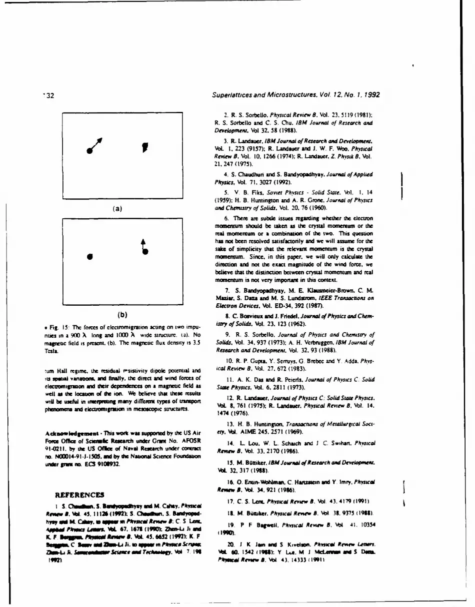
'32 Superlattices and Microstructures. Val. 72. No. 1. 1992
2. R. S. Sorbello. Physical Review 8. Vol. 23. 5119 (1981):R. S. Sortbello and C. S. Chu. IBM Journal of Research andDevelopment. Vol 32. 58 (1983).
3. R. Landauer. IBM Journal of Research and Development./ VoL 1. 223 (9157). R. Landauer and J. W. F. Vikio. PhysicalReview B, Vol. 10. 1266 (1974). R. Landauer. Z. Phvsik B. Vol.21, 247 (1975).
4. S. Chaudhun and S. Bandyopadhyay. Journal of Applied
Physics, Vol. 71. 3027 (1992).5. V. B. Fiks. Soviet Physics - Solid State. VolI. 1. 14
(1959); H. B. Huntington and A. R. Grone. Journal of Physics(a) and ChemistrY of Solids. Vol. 20. 76 (1960).
6. Thiere am subde issues regaiding whether the electroonmomentum should be taken as the crystal momemtum or thereal momentum or a combination of the two. This questionhas not been resolved satisfactorily andl we will assume for thesake of simplicity that the relevant momentum is the crystal
0 momentum. Since. in this paper. we will only calculate thedirection and not the exact magnitude of the wind force, webelieve that the distinction between crystal momentum and realmomentum is not very importnt in this context.
7. S. Dandyoipadhyay. M. E. Klausmecier-Brown. C. KNMaziar. S. Dana and M. S. Lundstrom. IEEE Transactions onElectron Devices. Vol. ED-34. 392 (1987.
(b) 3. C. Bosvieux and J. Friedel. Journal of Phrysics and Chem-
* Fig. 15: The forces of clectromigration acting on two impu- isirr of Solids. Vol. 2 3. 123 (1962).
nues in a 900 )k long and 1000) A wide structure. ta). No 9. R. S. Sorbello. Journal of Physics and Chemnistry ofmagetc field is present. (b). Thc magneuic flux dcnsity is 3.5 Solids. Vo. 34. 937 (1973); A. H. Vcrbruggen, IBM Journal ofTcsla. Research and Development. Vol. 32. 93 (1988).
10. R. P. Gupta. Y. Semivys. G. Brebec and YI. Adda. Phvs-
tumn Hall regime. fth residual i-sistiviiy dipole potential and ical Review B. Vol. 27. 672 ( 1983).its spwWa vananove aid finally, the direct and wind force of 11. A. K. Das and R. Peierls. Journal of Physics C. Solidelectionagranon mid their dependences on a magnetic field as State Physics. Vol. 6. 2811 (1973).well as the location of dhe ion. Wet believe that these results12R.Lnae.JualoPhscC:Sidti hyc.
will~ ~ ~ ~ ~ ~ ~ ~ ~ ~ ~~~~Vl 3e.eili ap gmn ifirn ye ftasot %L8 761 (1975); R. Landauier. Physical Review B. Vol. 14.phnms an plcrmgation in memsicopistuur. 1474 (1976).
13. H. B. Huntington, Transactions of Metallurgical Soca-
Acktnowledgement -This work wait aupponted by the US Air ery. Vol. AIME 245. 2571 (1969).Force Oftie of Scienekli Research under Gramt No. AFOSR 14. L. Lou. W. L. Schaich and I C. Swihars. Physical91-0211. by the US Offic of Naval Research under cotrc Revi.ew B. Vol. 33. 2170 (1986).no. N0O014-91-J-lS(0. aid by the National Science Foundationuider grant no. ECS 9103932. 15. M. B0tuker. IBM Jour"a of Research and Development.
'*,I 32. 317 (1913).
16. 0. Enuin-Wohimui. C. Hanzinem aid Y. Imry. Physical
REFERENCES Review 5. Vol. 34. 921 (1986).
l SC1~S.Si~phyauui.Caey.~rscal 17. C. S. Lemn Phvsicaj Review 8. Volý 4 3.4179 (199 1)Rinam S. Va. 45. 11126 (1992) S. Cosm~m. S. Bandyaesd- 18. M. Bihaiker. Physical Review B. Vblý 33. 935 (19111),hrqaid bt CA".ma pse inPkv=W iRteww : C S ait. 19, P F Bagwell. Physical Review B. Vol 41. 103544iliphd Phvn Law& Wo 67. 1678 (1990); Zen-Lj Ji wed (199m,.K.P F BUP Pit a~ Ret . %bL 45. 6652 (19921r K Fsumpm C 3mwo and a Zh Uji.m W m inPkwasserim 20, J K lain anid S Kivelson. Phyisicel Review Lenart.Zh~ A. 5 pWWb Sctasee &W Volmg 7.19g %bL 60. 1542 (1968): Y L..e. M J !eLimmin anid S Donr
191171 Phftyme Reviw 8. Vol 4 3, 143 33 119911

PHYSICAL REVIEW B VOLUME 47, NUMBER 19 15 MAY 1993-1
Current, potential, electric field, and Fermi carrier distributions around localized elastic scatterersin phase-coherent quantum magnetotransport
S. Chaudhuri and S. BandyopadhyayDepartment of Electrical Engineering, University of Notre Dame, Notre Dame, Indiana 46556
M. CahayDeparatment of Electrical and Computer Engineering, University of Cincinnati, Cincinnati, Ohio 45221
iReceived 3 April 1992; revised manuscript received 28 December 1992)
The spatial distributions of the current, Fermi carriers, electric field (due to space charges) and elec-trostatic potential in a disordered mesoscopic structure are calculated in the presence of arbitrary mag-netic fields. These distributions are useful in elucidating and visulaizing many features of quantum mag-netotransport, such as the formation of edge states at high magnetic fields and their near-perfecttransmittivity, the evolution of the integer quantum Hall effect, the creation of magnetic bound statesaround an impurity, the magnetic response of current vortices that form as a result of quantum interfer-ence between scatterers and the walls of a quantum wire, the dependence of the quantized-conductancesteps in a backgated quantum wire on an applied magnetic field, the behavior of residual-resistivity di-poles and the electrostatic space-charge potential in a magnetic field, the dependence of the sign of themagnetoresistance on the impurity configuration, etc. We examine the current, Ferm carrier concentra-tions, electric field, and both chemical- and electrostatic-potential profiles associated with each of thenephenomena, and relate them to the observed terminal characteristics in each case.
1. INTRODUCTION all show quenching phenomena. We also found why thesign of the magnetoresistance of a quantum wire could
Many features of quantum magnetotransport in a depend on the position of a single impurity inside themesoscopic structure can be understood by examining the wire. These, and the nature of other phenomena, becomespatial distributions of the current, potential, electric very clear when one examines the spaa patterns offield, and Fermi carriers around elastic scatterers in the current, carrier concentration, and electrostatic or. chem-presence of a magnetic field. In this paper, we have cal- ical potentials. The spatial distributionm are not only ofculated such spatial patterns from a fully microscopic great importance in understanding the origin and the de-quantum-mechanical formalism based on the Schr6dinger tailed physics of many quantum magn etransport phe-equation. These spatial distributions are, of course, not nomena, but they often determine the nature of certain".precise" in view of the Heisenberg uncertainty principle physical phenomena such as electromigration.which prohibits simultaneous definition of both the posi- This paper is organized as follows. In Sec. II, wetion and the momentum of an electron; instead they briefly present the quantum-mechanical theory used inshould be viewed as spatial distribution of quantum- computing the two-dimensional spatial distributions ofmechanical averages (or expected values) of the corre- current, Fermi carrier concentration, potential, and inter-sponding quantties. These patterns help in understand- nal electric-field profiles around localized scatterers in theing several quantum transport phenomena and provide presence of a magnetic field. In Sec. Ill. we present thedirect visualization of the associated physics. For exam- results for a disordered GaAs quantum wire containing apie. we show the spatial distribution of the current car- vanable number of impurities. We show the spatial pat-ned by edge states in a quantum wire at high magnetic terns associated with various magnetotransport phenom-field. The current patterns clearlv show the high ena in both single-channeled and multichanneled trans-S transmittivity which is responsible for the quantization of port Such spatial patterns were presented by us in thethe Hall resistance in the quantum Hall regime. We also limit of coherent diffusive transport (in the absence of anyshow how current circulates around an impunty when a magnetic field) earier.' Others have presented such pat-magnetic bound state forms. The recovery of the quanti- terns in the limit of coherent ballistc transport with nozation of conductance steps in a dirty quantum wire by scattering whatsoever.: To our knowledge, we are thethe appbication of a magnetic field is known to be associ- first to present such patterns in the cohemet difflw•em re-,ited with the suppression of hackscattering. And the gime in !he presence ot a magnetic field.current patterns thai we obtain show this %ers c'learivThe onset of the integer quantum Hall effect is :aused h% II. THEORYthe edges of a quantum wire tbecoming pertectl% %m~xthN;uipt•ential surface% and our ýhemical potential profile% rhe theor, for our :akulations of the current and car-demOnstrate thns vtnkingiw The magnetic responte ot rier dermstv patterns in a juantum wire in the absence of.urreist vosuces. eimtrostatic potential, and eiectr1c fied . magnetic bed has been Inscribed in Ref. I Har, we
4' :2e,. c 1941 T'e AiiPibm'iil 1S1om•s

12650 S. CHAUDHURI. S. BANDYOPADHYAY. AND M. CAHAY 47
repeat only the basic features. We consider a mesa asshown in Fig. I which is single moded in the z direction,i.e., only a single subband is occupied in that direction).but multimoded in the y direction.
The time-independent Schr6dinger equation describingsteady-state electron transport in this confined quasi-one-dimensional disordered structure under a magneticfield is
- e A) bV E) FIG. I. A quasi-one-dimensional quantum wire containing a-- %b- Vib--Ei, () random array of elastic scatterers. The structure is single mod-
2m* ed in the z direction but multimoded in the y direction. The
where p is the momentum operator, m * is an isotropic magnetic field is applied in the z direction.
effective mass. and the potential energy V consists of twoterms,
a2m 2M I_ y 1V = V(ix.Y)=Vc(y = V. p).,- V, y) a -" 4- E6(y)- 6(y)
+ 21 kly)-k2,oy)=O ,(5)
The first term gives the effect of the confining potential in 2
the y direction and the second term is due to impurities, with I being the magnetic length given by I -We assume hardwall boundary conditions in the y direc- The wave function 0(y) is found by solving the abovetion and 8 potentials for the impurities so that we have equation numerically using a finite difference scheme as
described in Ref. 3. This method also gives the energydispersion relations E vs k. for the .'arious hybrid mag-
V,mp(Xy)=Y 8(x -x, )6(y -Y, I, (3) netoelectric subbands that arise from the confining effects
of the magnetic field and the confining potential in the ydirection. A set of computed energy dispersion relations
where s is the total number of impurities in the structure are shown in Fig. 2. After calculating the energy disper-and the summation extends over all the impurities. The sion relations, we choose a certain energy E (which weposition of the ith impurity is denoted by (xi,y,). call the Fermi energy E ) and find the corresponding x-
The wave function 0b0 in the absence of impurities can directed wave vectors k~ for various magnetoelectric sub-be written as bands (indexed by p) from the dispersion relations. These
wave vectors k F and the wave functions 6 (Y) are used to&°(x,y)=e'6(y) (4) determine the total wave function b,,(x,y, (in the pres-
ence of impurities) for an electron injected with the Fermiwhere k, is the x-directed wave vector and 6(y) satisfies energy EF from the subband m in the left contact. The
the eigenequation wave function is given by
w .4 ,, x )exp• ik x )¢ 4 (y) + B., ( x)exp( ik Fp X)6_ P(y)Th (X )_ P_ (6)
IIwhere the summation extends over "oh propagating and only have to evaluate the coefficients A,,,(x) and Bxevanescent modes (the total number of modes considered to determine the wave function of Fermi electrons every-ts MI. The subscript -p indicates that the quantity cor- where. If we know these coefficients at any positionresponds to a wave function with an oppositely directed ix 0 ,y) in the structure, then the coefficients at any other'elocity as compared to the one with a subscript p. position (x 1 ,y) can be found from
When the wave function is written in this form (i.e.,
each mode is normalized by the square root of the corre-sponding group velocity), all propagating modes at the r,)r , t 1 2I f,Ferm energy carry the same current. This is consistent !r(7,with the well-known cancellation of the velocity and den- -
sity of states in quasi-one-dimensional structures which where i1 is a column vector of length M whose elementscauses every mode to carry the same current.' We now are A,,l(X,') , A, 2txo), A, 3 lxo) 4,'xO), 1, is a

47 CURRENT. POTENTIAL, ELECTRIC FIELD, AND FERMI ... 12651
0 .0. sequently, the elements of the scattering matrix cannot be
-8 '/ found by the normal prescription of Ref. 1. The method_ .,______.. ... ...... _E, for finding these elements is described in the Appendix.
,s r // \\Once we have evaluated the scattering matrices, we' \ X\--• ,' 'have found all the quantities that we need in order to
evaluate the wave function of Fermi electrons everywhere2 -,in the structure. From this wave function, we calculate
- •i\ \\ • / ,' all quantities of interest.
\\ / In linear-response transport at low temperatures, only-J electrons at the Fermi level carry a net current. There-
/; / ' fore, the two-dimensional wave function #.(x,y) of elec-/ /- /trons in the mth subband allows us to calculate the con-
tribution of that subband to the two-dimensional current4 - / /density. This is given by
2• J (x,y)]
34 .03 02 -01 3 01 22 23 04 +x10 nmi Mi
FIG. 2. The eanerg dispersion relations for the hybrid m The Fermi carrier concentration due to the contributionS d wreo id 20) A a a from the mth subband is defined by us as
mipnn uc flux dsety of 1.5 T. The solid lines are the results of n,. (xy)t# m,(xy)I2 . (10)ezact numerical calculatitio whereas the broken lines are theresults of the smeamamcal Bohr-Sommerfeld quantization rule. The total current density is found by vectorially adding
the contributions from all propagating modes and the to-tal Fermi carrier concentration is found by the scalar ad-dition of the contributions from all propagating modes.
column vector of length M whose elements are B. (xo), Note that no weighting by the density of states is neces-B,,aI(Xo), B.3(Xo)' B,.A(Xo). re is a column vector of sary in the summation since the wave functions have beenlength M whose elements are A,, 1(x 1 ),A. 2(X1 ), normalized by the square root of velocity which takesA,(3x,)"" AN(x I), and r, is also a column vector of care of the density of states.length M whose elements are B.,I(xl), B,, 2(x),
,..3(x) •.. B,(xi). The coefficients t,1,412,421, and J,,(X,y): • .J,(x,y) ,t 2 are each M X M matrices and the square matrix in Eq. propaasaa n.s (11 )(7) is the so-called transfer matrix for the section of the nai(x,y)= nstructure between x =x 0 and x ,. propaaazaas
The above equation allows us to determine the Finally, we find the electrostatic space-charge potentialcoeffkients AOP(z,) and Rap(xI) (and hence the wave V(xy) from the relation4"'76function) at any arbitrary location x1 if we know thewave function [or the coefcients A,,(xo) and B..(xo)] I I*1,.(X,Y) 2'P1+I02,.(X,Y)I 2IA 2
at any one point x =x 0 in the device as well as the eV(xy)= p 1212.transfer-matrix elements. We do know the wave function I loit..,I+I*2,mat the left contact (x -0). We assume that for injection p"Vafin$
into the mth mode, the wave function is given by scatter- (12)mn| states' (this is our boundary condition)where ul and /2 are the chemical potentials in the two
exp~ik.x )•,(y) contacts of the quantum wire, 01., is the wave functionV I VO-, corresponding to injection in mode m (with energy pA)
from the left contact, and 02.,, is the wave function for+I RP expi(8k)_•xi_(y) injection in mode m (with energy I2) from the right con-+()- i, vT tact. The above equation is derived from the Poissonequation and is valid only for (a) linear-response trans-
so that A,,•x =0- =6,,, (Kronecker delta) and port, (b) situations where the potential variation ofB,,,x =0- =R,,. Therefore, we can find the wave V(x,y) is smooth on the scale of the screening length,function anywhere in the structure using Eqs. (6) and (7) and (c) when the Fermi wavelength is considerably small-if we can find the elements of the appropriate scattering er than the screening length. When these conditions aremastrices in Eq. (7). In the absence of a magnetic field, not satisfied, the actual Poisson equation must be solvedthes elenems an fidrly easy to find,' but for nonzero simultaneously with the Schr6dinger equation, rathermagnetic bid th, wave fuanctions of the various sub- than using the simplified equation (12). That is numeri-band states at the Fermi energy are not orthogonal. Con- cally much more demanding because in the Poisson equa-
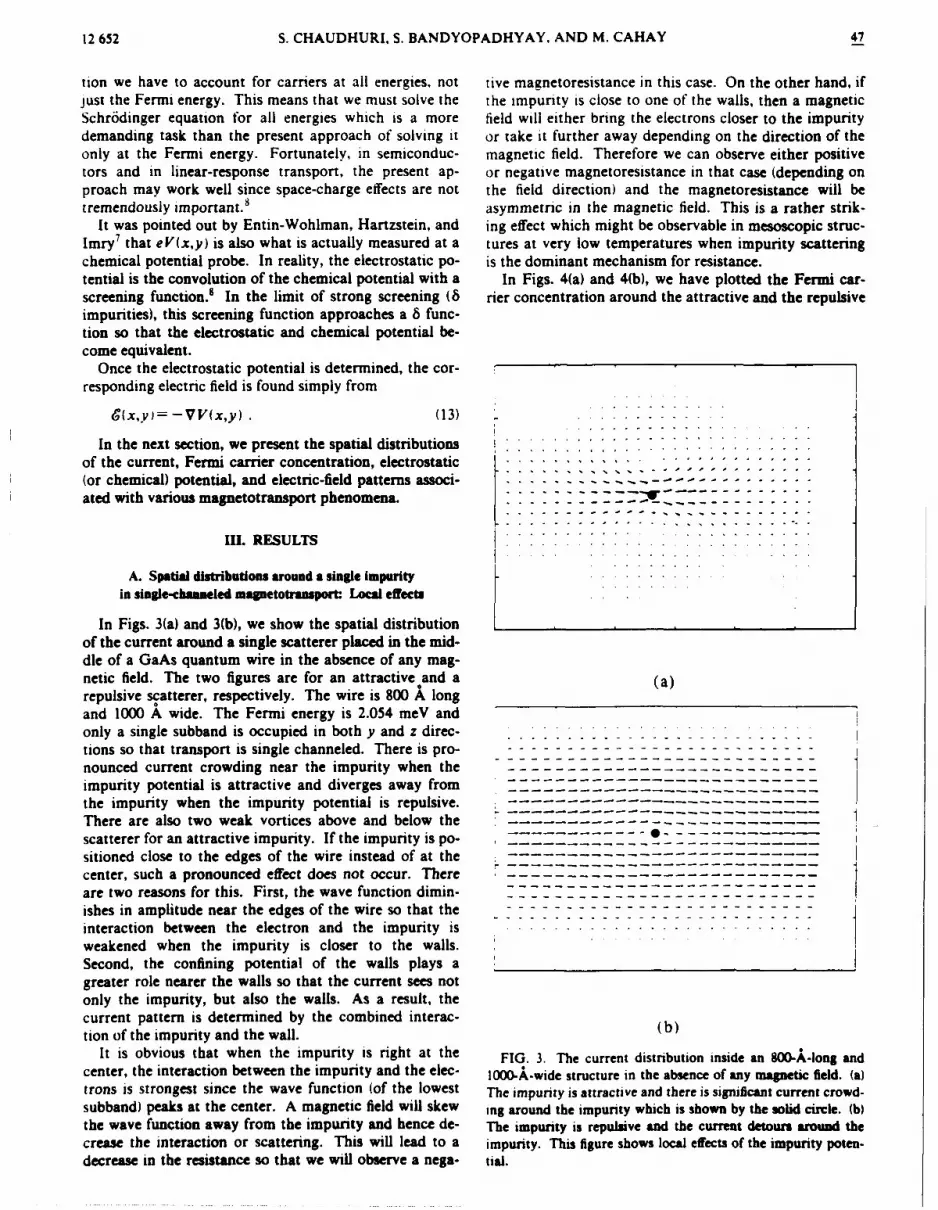
12652 S. CHAUDHURI, S. BANDYOPADHYAY. AND M. CAHAY 47
tion we have to account for carriers at all energies, not tive magnetoresistance in this case. On the other hand, ifjust the Fermi energy. This means that we must solve the the impurity is close to one of the walls, then a magneticSchr6dinger equation for all energies which is a more field will either bring the electrons closer to the impuritydemanding task than the present approach of solving it or take it further away depending on the direction of theonly at the Fermi energy. Fortunately, in semiconduc- magnetic field. Therefore we can observe either positivetors and in linear-response transport, the present ap- or negative magnetoresistance in that case (depending onproach may work well since space-charge effects are not the field direction) and the magnetoresistance will betremendously important.8 asymmetric in the magnetic field. This is a rather strik-
It was pointed out by Entin-Wohlman, Hartzstein, and ing effect which might be observable in mesoscopic struc-Imry 7 that eV(x,y) is also what is actually measured at a tures at very low temperatures when impurity scatteringchemical potential probe. In reality, the electrostatic po- is the dominant mechanism for resistance.tential is the convolution of the chemical potential with a In Figs. 4(a) and 4(b), we have plotted the Fermi car-screening function.! In the limit of strong screening (8 rier concentration around the attractive and the repulsiveimpurities), this screening function approaches a 8 func-tion so that the electrostatic and chemical potential be-come equivalent.
Once the electrostatic potential is determined, the cor-responding electric field is found simply from
6(x,y = -VV(x,y) . (13) .-..........
In the next section, we present the spatial distributions .. . . . .
of the current, Fermi carrier concentration, electrostatic . .. . .
(or chemical) potential, and electric-field patterns associ- .............ated with various magnetotransport phenomena. - - - •'_ - - -"
11 . FS LT . . . . . . . . . . . . . .. . . . . .. . -. .II1. RESULTS i i i i i i ii i • i i~
A. Spatial distributions around a single impurity ......in single-chaaneled magnetotrasport: Local effects
In Figs. 3(a) and 3(b), we show the spatial distribution
of the current around a single scatterer placed in the mid-dle of a GaAs quantum wire in the absence of any mag-netic field. The two figures are for an attractive and a (a)repulsive scatterer, respectively. The wire is 800 A longand 1000 AL wide. The Fermi energy is 2.054 meV andonly a single subband is occupied in both y and z direc- . . . . . . . . . .. . .. .. . .
tions so that transport is single channeled. There is pro-
nounced current crowding near the impurity when the- --- -- -------------
impurity potential is attractive and diverges away fromthe impurity when the impurity potential is repulsive.
There are also two weak vortices above and below the ------
scatterer for an attractive impurity. If the impurity is po--- - - - - - - - - - ---
sitioned close to the edges of the wire instead of at the -.
center, such a pronounced effect does not occur. There
are two reasons for this. First, the wave function dimin-ishes in amplitude near the edges of the wire so that the - - - - - - - - - - - - - - - - - - -- - - - - - -
interaction between the electron and the impurity is ............. _._._._._._._._._._._._..
weakened when the impurity is closer to the walls.Second, the confining potential of the walls plays a __ . . . .greater role nearer the walls so that the current sees notonly the impurity, but also the walls. As a result, thecurrent pattern is determined by the combined interac- (b)tion of the impurity and the wall.
It is obvious that when the impurity is right at the FIG. 3. The current distribution inside an 800-A-long andcenter, the interaction between the impurity and the elec- 1000-A-wide structure in the absence of any magnetic field. (a)trons is strongest since the wave function (of the lowest The impurity is attractive and there is significant current crowd-
subband) peaks at the center. A magnetic field will skew ing around the impurity which is shown by the solid circle. (b)the wave function away from the impurity and hence de- The impurity is repulsive and the current detours around thecrease the interaction or scattering. This will lead to a impurity. This figure shows local effects of the impurity poten-decrease in the resistance so that we will observe a nega- tial.

47 CURRENT, POTENTIAL, ELECTRIC FIELD, AND FERMI ... 12653
pole formation in most cases. although it may sometimesalso enhance the dipole formation depending on the im-purity configuration, i.e.. the exact phase relationshipsbetween the interfering waves. Therefore, even thoughthe dipole formation is a local effect in itself, the size andorientation of the dipoles are significantly affected bynonlocal quantum interference effects.
In Figs. 5 and 6, we plot the electrostatic (or chemical)potential and electric-field profiles. For these figures, weassume that/1t =2.056 meV and /u2=2.052 meV. We donot exactly see the characteristic electric-field distribu-tion of a dipole since the "poles" of the dipole are not"isolated" charges; they are "extended" charges. Theplots are presented for both attractive and repulsivescatterers. They are very different when the impurity po-
a) tential is attractive (which corresponds to majority car-
rier transport) as opposed to the case when it is repulsive(minority carrier transport). In the case of attractive im-purities, there can be a building up of evanescent statesaround the impurities associated with the formation ofquasibound donor states. 10 These may help in dipole for-mation.
The application of a magnetic field causes dramaticchanges in the current, carrier concentration, electrostat-ic potential, and electric-field profiles. We show these
(b)
FIG. 4. The Fermi carrier concentration profile for the struc.ture of Fig. 3 in the absence of any magnetic field. (a) The im-purity is attractive; (b) the impurity is repulsive.
impurity of Figs. 3(a) and 3(b) in the absence of any mag-netic field. As expected, in the case of the attractive im-purity, we see a sharp spike (accumulation of electrons)around the impurity where-the current crowding occurs.The electrons are attracted to the impurity by electrostat-ic attraction. In the case of repulsive impurity, the con-centration is depleted where the impurity is positionedbecause of electrostatic repulsion. In Fig. 4(a), we seethat there is a building up of electrons to the left of thescatterer and a deficit to the right. This happens becausethe impurity strongly reflects the incoming electronswhich build up to the left. Because of the excess negativecharge on one side and a deficit on the other, we expect adipole to form. This is the residual-resistivity dipole asdiscussed by Landauer. 9 We can contrast these figureswith the profiles that were presented in Ref. I which con-sidered only multiple-impurity systems. When a largenumber of impurities are placed inside the wire, the localcharge accumulation and depletion effect that causes a di-pole to form is usually diminished because of quantum-mechanical interference between waves reflected from the FIG. 5. The electrostatic- (or chemical-) potential profile in-various impurities. This quantum-mechanical interfer- side the structure of Fig. 3 in the absence of any magnetic field.ence is a nonlocal effect which tends to inhibit local di- (a) Attractive impurity; (b) repulsive impurity.

12 654 S. CHAUDHURI, S. BANDYOPADHYAY, AND M. CAHAY 47
effects for the single attractive impurity in Figs. 7(a), 7(b), the forward current. There is also, however, a small7(c), and 7(d) which are to be compared with Figs. 3(a), reverse-traveling current component close to the walls.4(a), 5, and 6, respectively. This component was explained in Ref. I I (which dealt
In Fig. 7(a), we have plotted the current inside the wire with edge states in ballistic transport as opposed toin the presence of a magnetic-flux density of B = 2. 18 T. diffusive transport) as being due to the classical cyclotronAD other conditions correspond to the case of Fig. 3(a). trajectories (skipping orbits) having their velocitiesComparing with Fig. 3(a), we find that current crowding directed opposite to the net current flow adjacent to thehas disappeared and the two weak vortices have been edges. At higher magnetic fields, this reverse componentquenched. The sample now no longer exhibits localized diminishes so that backscattering is suppressed evenmagnetic moments due to the vortices. In addition, there more. In other words, the transmittivity of the edgeis a significant reduction of the backscattered current states are very high at high magnetic fields. This agreescomponent. A similar reduction in backscattering is ob- with Bfittiker's picture of the integer quantum Hallserved for a repulsive impurity also, except that it takes a effect12 in which perfect transmission of edge states waslower magnetic field to reduce the backscattering by the invoked to explain quantization of the Hall resistance andsame amount. The current pattern in Fig. 7(a) clearly vanishing of the longitudinal resistance.shows that edge states have formed and carry the bulk of In Fig. 7(b), we show the concentration profile of the
Fermi carriers in the presence of a magnetic field of 2.18T. The concentration piles up near an edge because ofthe Lorentz force skewing the wave function towardsthat edge. Note that there is no longer a buildup of elec-
S. ..... trons to the left of the scatterer and a deficit to the rightS. ..... since the buildup is due to reflection (backscattering) and
S: - . this has diminished significantly. In fact, at high enough
-:- - magnetic fields, backscattering is always reduced. There-• . -, •-' , .fore, in general, residual-resistivity dipoles will be des-
.. troyed by an external magnetic field if it is of high enough• • - - •, .... magnitude.
... .. " - "In Fig. 8(a), we show the conductance of the structure.of Fig. 3(a) versus the Fermi energy at a magnetic field of
S. •3.5 T. There is only one attractive impurity in the struc-.. .. ture placed at the center. A pronounced dip in the con-
* ductance is seen at an energy of 3.82 meV. At this ener-gy, a magnetic bound statei 3 forms around the impurity
. ......... which causes the transmission (and hence the conduc-tance) to decrease sharply. This state forms at about thesame energy for a repulsive scatterer. The correspondingcurrent profile is shown in Fig. 8(b). We find that there is
(a) only a small amount of net current traveling from onecontact to another when a magnetic bound state forms
.. ........... and the bulk of the current circulates around the impuri-ty. These magnetic bound states are quite different fromthe quasidonor statesl° which are also bound states givingrise to dips in the conductance characteristics. There aretwo major differences between magnetic bound states andquasidonor bound states. First, the former occurs re-gardless of whether the impurity is attractive or repul-sive, whereas the latter forms only when the impurity isattractive. Second, the current patterns are verydifferent. In the case of magnetic bound states, thecurrent circulates around the impurity but in the case of
quasidonor states, no such circulating current patternneeds to form.' Finally, the carrier-concentration profilesare also quite different. In the case of magnetic boundstates, the concentration builds up around the impuritybut right at the impurity it drops sharply. This is shownin Fig. 8(c). Although the carriers may accumulate
(b) around the impurity even in the case of quasidonor stateformation (owing to the buildup of evanescent states), the
FIG. 6. The electrick4eld profile inside the structure of Fig. 3 effect is much less pronounced. Finally, Fig. 8(d) showsin the absence of any magnetic field. (a) The impurty is attrac- the electrostatic-potential profile when a magnetic boundtive; (b) the impurity is repulsive, state forms.

47 CURRENT, POTENTIAL, ELECTRIC FIELD, AND FERMI ... 12 655
B. Spatial distibuions for multiple impurities 3-8 and the Fermi energy is 2.41 meV. There are twoin diagle-chaueled tramprt: Nonlocal effects vortices in the current pattern. They have opposite cir-
culations and produce antiparallel localized magneticIn structures where multiple impurities are present, moments. As we turn on a magnetic field [see Fig. 9(b)],
vortices form in the current pattern as a result of quan- we see immediate quenching of one vortex accompaniedtum interference between waves reflected from the walls by a slight reduction in the strength of the other. Thisand various impurities.' These vortices are a striking aft- different behavior for the two vortices can be explainedermath of nonlocality in phase-coherent quantum trans- by the fact that for one vortex, the Lorentz force tends toport. They are not centered around impurities since they produce a circulation in a sense opposite to that of theare a consequence of nonlocal effects, and their positions, vortex. Consequently, even a very low field is sufficient toas well as strengths, depend on the impurity quench this vortex. The resultant change in the quantumconfiguration. In Fig. 9(a), we show the current distribu- interference between the scatterers cae the aibr vor-tion in a sample with two impuriti s without any magnet- tex to weaken as well, even though it has a circulationic field present. The structure is the same as that in Figs. pattern in the same direction as that produced by the
(a))
St _I I •~ J , , I ! I ,
I
(c) (d)
FIG. 7. The spatil distributions in the structure of Fig. 3 in a magnetic-flux density of 2.18 T. The impurity is attractive. (at) Th'ecurrent distriblo. The bulk of the forward current is carried by edge states. The small backacttere compoeont nea the wlwes explained in Ref. 9. This fglure should be compared with Fig. 3(-a. Note that the local effects of the impurity potntil are inhib-ited by the magnetic field. (b) The Fermi carrier concentration distribution which peaks near an edge becaue of the Lormat forceskewngl the waw unction towarsthadt edge. (c) The electrostatic (or chemica) potential proflge which shows •mo¢th eq..poesstasurfaces thi, aouga wall sad pa along the other. The lonlgitudinal four-terminal resstance that will be measured by attchagio welt-age probes - the edges wi be zero showing the occurrence of the integer quantum Hall effect. (d) The electric-field d~tributio.which us noasos oly at the center of the wire.
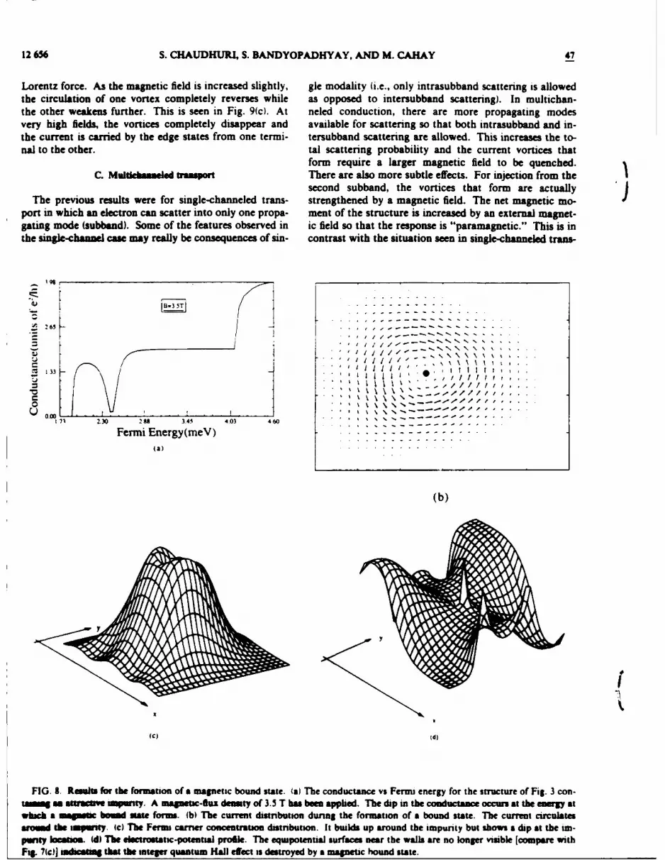
12 656 S. CHAUDHURIL S. BANDYOPADHYAY, AND M. CAHAY 47
Lorentz force. As the magnetic field is increased slightly, gle modality (i.e., only intrasubband scattering is allowedthe circulation of one vortex completely reverses while as opposed to intersubband scattering). In multichan-the other weakens further. This is seen in Fig. 9(c). At neled conduction, there are more propagating modesvery high fields, the vortices completely disappear and available for scattering so that both intrasubband and in-the current is carried by the edge states from one termi- tersubband scattering are allowed. This increases the to-nal to the other. tal scattering probability and the current vortices that
form require a larger magnetic field to be quenched.C. Mmlchainaled ramplon There are also more subtle effects. For injection from the
second subband, the vortices that form are actuallyThe previous results were for single-channeled trans- strengthened by a magnetic field. The net magnetic mo-
port in which an electron can scatter into only one propa- ment of the structure is increased by an external magnet-gating mode (subbend). Some of the features observed in ic field so that the response is "paramagnetic." This is inthe sine-channel case may really be consequences of sin- contrast with the situation seen in single-channeled trans-
- -I - - - - -
2 265
- , / -.. .. s,, ' . * \ . .
133 / , ,l-
U O.
I' I
2.30 299 3.45 4.03 460
Fermi Energy(meV).. - - --- - - - -Fermi nergy~eV) . ...............
(a)
(b)
(C) d
FIG. S. Results for the formation of a magnetic bound state. (a) The conductance vs Fermi energy for the structure of Fig. 3 con-tammlg an stowtmupuity. A magnstic-fluz demty of 3.5 T haa been applied. The dip in the conductance occurs at the enry atWhich a mgnuc I M sd ane forms. (b) The current distnbution during the formation of a bound state. The current circulatesaromnd the ilmpiy. (c) The Fermi carrier concentration distribution. It bulds up around the impurity but shows a dip at the im-purity locaon. 1d) The electrostatic-potentil prodle. The eqwpotential surfaces near the wills are no longer visible [compare withFig. 7W)] indicating tiht the integer quantum Hall effect i destroyed by a magnetic hound state.

47 CURRENT. POTENTIAL, ELECTRIC FIE]LD, AND FERMI... 12 657
port (Figs. 9) in which the response was "diamagnetic." at high magnetic fields owing to the formation of edgeIn Fig. 10, we have plotted the conductance versus states with high transmittivity.1'7 1 The quantization for
Fermi energy of a GaAs quantum wire of length 900 the higher steps is generally worse and does not improveand width 1000 A containing four attractive impurities, very much with increasing magnetic field since theThe conductance shows quantized steps associated with transmittivities of the higher subbands are always lowersubband filling.1' The results are plotted for magnetic- The real-space edge-state trajectories at the two edges
flux densities of B =0 and 3.5 T. The quantization of the corresponding to the higher subbands are spattally closerconductance steps is quite poor in the absence of a mag- to one another than those corresponding to the lower
netic field because of significant backscattering from the subbands. This causes increased coupling between theimpurity ....6 When a magnetic field of 3.5 T is turned higher subband edge states and hence increased back-on, the steps become wider and the lowest steps become scattering.much smoother. The steps become wider since the sub- In Figs. 1 (a), 11 (b), and 11 (c), we plot the current dis-band separation in energy increases with magnetic field tributions around a single attractive impurity when two
and the widths of the steps are equal to these separations. subbands are occupied. The three figures are the currentIn addition, the lowest steps become smoother since the patterns due to injection from the first subband, thetransmission probabilities of the lowest subbands increase second subband, and the resultant current pattern, re-
. . -. . . . . .-
---------- ----------.
----------------S .. . . . ... .. . . . . . .- - , r o , ,,.,• ... •
(a) (b)
t ......" ............ . . . . .. . . . . . . . . . .
i . .. . . . . . . . .iI-I
(C)
FIG. 9. The spatal distnbutons for a 900-A-long and 1000-A-wide structure conuuning multiple impurities. (a) The currentprofile in zero magntc ield showing the formation of two strong vortices due to quantum interference between the scatterers andwall. (b) The quenching of one of the vortices and weakening of the other by a magnetic flux density of 0.08 T. (c) Complete changein the vortex patterm and formation of edge states at a flux density of I T.
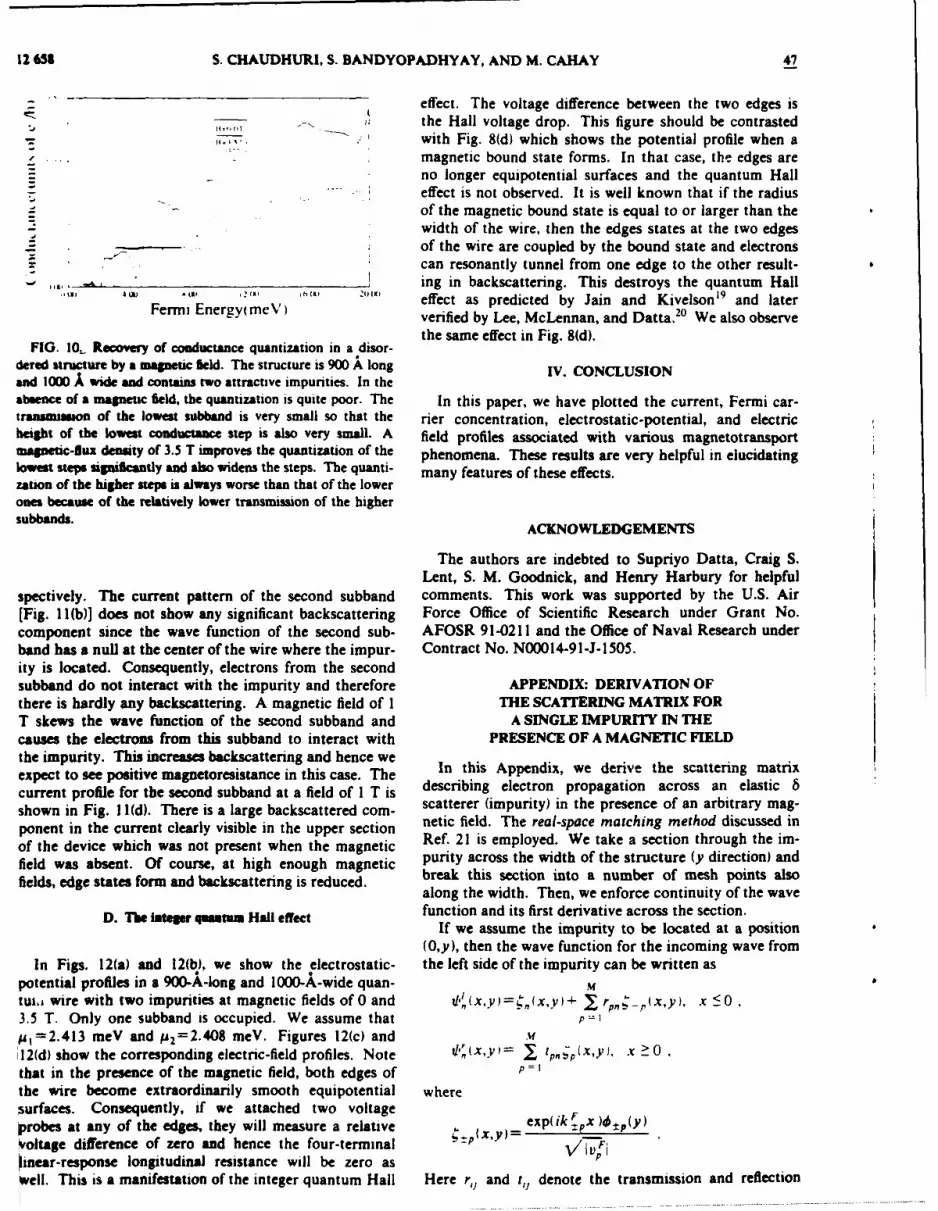
12658 S. CHAUDHURI, S. BANDYOPADHYAY, AND M. CAHAY 47
effect. The voltage difference between the two edges isthe Hall voltage drop. This figure should be contrastedwith Fig. 8(d) which shows the potential profile when amagnetic bound state forms. In that case, the edges areno longer equipotential surfaces and the quantum Halleffect is not observed. It is well known that if the radiusof the magnetic bound state is equal to or larger than thewidth of the wire, then the edges states at the two edgesof the wire are coupled by the bound state and electronscan resonantly tunnel from one edge to the other result-
S,.ing in backscattering. This destroys the quantum Hall4 .. AIR . W. . "1 IN effect as predicted by Jain and Kivelson' 9 and later
Fermi Energy(meV) verified by Lee, McLennan, and Datta. 20 We also observe
the same effect in Fig. 8(d).FIG. 10._ Recovery of conductance quantization in a disor-
dered structure by a magnetic ield. The structure is 900 A long IV. CONCLUSIONand 000 A wide and contains two attractive impurities. In theabsence of a magnetic field, the quantization is quite poor. The In this paper, we have plotted the current, Fermi car-traunsm of the lowest subband is very small so that the rier concentration, electrostatic-potential, and electricheight of the lowest conductance step is also very small. A field profiles associated with various magnetotransportmagnetic-flux density of 3.5 T improves the quantization of the phenomena. These results are very helpful in elucidatinglowest steps signifcantly and also widens the steps. The quanti- many features of these effects.zaton of the higher steps is always worse than that of the lowerones because of the relatively lower transmission of the highersubbands. ACKNOWLEDGEMENTS
The authors are indebted to Supriyo Datta, Craig S.Lent, S. M. Goodnick, and Henry Harbury for helpful
spectively. The current pattern of the second subband comments. This work was supported by the U.S. Air[Fig. I 1(b)] does not show any significant backscattering Force Office of Scientific Research under Grant No.component since the wave function of the second sub- AFOSR 91-0211 and the Office of Naval Research underband has a null at the center of the wire where the impur- Contract No. N00014-91 -J-1505.ity is located. Consequently, electrons from the secondsubband do not interact with the impurity and therefore APPENDIX: DERIVATION OFthere is hardly any backscattering. A magnetic field of 1 THE SCATTERING MATRIX FORT skews the wave function of the second subband and A SINGLE IMPURITY IN THEcauses the electrons from this subband to interact with PRESENCE OF A MAGNETIC FIELDthe impurity. This increases backscattering and hence weexpect to see positive magnetoresistance in this case. The In this Appendix, we derive the scattering matrixcurrent profile for the second subband at a field of 1 T is describing electron propagation across an elastic 8
shown in Fig. 1 (d). There is a large backscattered com- scatterer (impurity) in the presence of an arbitrary mag-
ponent in the current clearly visible in the upper section netic field. The real-space matching method discussed inof the device which was not present when the magnetic Ref. 21 is employed. We take a section through the im-
field was absent. Of course, at high enough magnetic purity across the width of the structure (y direction) and
fields, edge states form and backscattering is reduced. break this section into a number of mesh points alsoalong the width. Then, we enforce continuity of the wave
D. The hateger qmutum Hall effect function and its first derivative across the section.If we assume the impurity to be located at a position
(O,y), then the wave function for the incoming wave fromIn Figs. 12(a) and 12(b), we show the electrostatic- the left side of the impurity can be written as
potential profiles in a 900-A-long and 1000-A-wide quan- Ma
tutj wire with two impurities at magnetic fields of 0 and tV, ((x,y)= . (x,y)-4- 1 rpa,, (x,y), x 03.5 T. Only one subband is occupied. We assume that p -
jut=2. 4 13 meV and m2=2.408 meV. Figures 12(c) and M12(d) show the corresponding electric-field profiles. Note ,', (X,y) • y x I 0that in the presence of the magnetic field, both edges of P =1
the wire become extraordinarily smooth equipotential wheresurfaces. Consequently, if we attached two voltage (probes at any of the edges, they will measure a relative exp(ik___ ___ _p(y)
voltage difference of zero and hence the four-terminal p _/.VFj
lnear-response longitudinal resistance will be zero as
well. This is a manifestation of the integer quantum Hall Here r,, and t,, denote the transmission and reflection

47 CURRENT, POTENTIAL, ELECTRIC FIELD, AND FERMI ... 12659
coefficients from the jth mode to the ith mode. where the individual elements t.r, etc., are themselvesFor the incoming wave from the right side of the im- M X M matrices and M is the total number of modes
purity, the wave function can be written as (propagating plus evanescent).M• We now enforce the continuity of the wave function
d,(x, y)= t x, y)+ •. r,.-(x.y), x __0 , and its first derivative at all mesh points. This allows usp= to write the set of real-space mode-matching equations
for the incoming wave from the left
tbl (0,yi )=r(O,yi) for all possible i
The scattering matrix across the impurity is defined as
S= t r' (O,yj)= 2m* y-yOy)
--------------y6 y-------~i
------------------------------
. .. . . . . .... . ... ... . ------ ----- ------ -----
S. . .. . .. . . . . .. . . . . .
(a) (b)
. . . . . . . . . . . . . . . . . .... . ...........................
---------------------------
----------------
.. . . . . . . . . . . . . - - --.. ..-.-.- - - - - -
.. -- - - -. -.. . .. - , . . . . . . . . . .
I -
*------------------------------------------------
. . . . . . . . . . . . . . . ... . .
(c) (d)
FIG. 1 I. Spatial distributions for multichanneled conduction in a structure of length 800 A and width 1000 A with one attractive
impurity. (a) Current distribution for injection from the lowest subband only at zero magnetic field. (b) Current distribution for in-jection from the second subband only at zero magnetic field. Not much backsc,"attering is observed since the second subband wavefunction has a null at the impurity location. (c) The total current distribution at zero magnetic field. (d) The current distribution at aflux density of I T for injection from the second subband only. Significant backacattering is observed compared to (b) since the wavefunction of the second subband is skewed towards the impurity by the magnetic field which increases the interaction of the electronsin the second subbend with the impurity.

12 660 S. CHAUDHURI, S. BANDYOPADHYAY, AND M. CAHAY 47
where .v, is the ith mesh point along the y direction. rt '= I _ I.At the location of the impurity, the derivative of the V t.
wave function is discontinuous by a 6 function; else-where, it is continuous. Exact treatment of this condition r l,, - _
is not possible. We average the quantities over the inter- v -val containing the impurity by multiplying every equa- t2 ik1 =,tion by som e averaging function and then integrating t2,, I -r-- _.( y o ioover the interval. For our case, we simply choose the i VV) h' V U1averaging function as r -r2,, = --- • I
$ jy )S_
(n f j -I dy VVyhn-.-i1 f Y,, d .
-Y. - -- y" Y.
[ij
Substituting for vb, and a,, the above equations may be ikj .rewritten in matrix notation as dj , _ I +.0
vvci j vj
't2 r2 ,I d1 (Yi 'YO)
where =0 (yi*y•. 0 .
Y
! r
0S
(C) (d)
FIG. 12. Electrostatic- (or chemical-) potential and electric-field profiles inside a structure with two attractive impurities. (a) Po-tential profile in the absence of any magnetic field. Significant potential variations are observed. (b) The potential proile at amagnetic-flux density of 3.5 T. The edges have become eqwipotential surfaces showing the occurrence of the integer quantum Halleffect. (c) The electric-fleld profile in the absence of any magnetic-field. (d) The electric-field profile at a magnetic-flux density of 3.5T.
47 CURRENT, POTENTIAL, ELECTRIC FIELD, AND FERMI. .. 12661
In a similar manner, the equations for the transmission Current conservation requires that the scattering matrixand reflection coefficients for the incoming waves from be unitary and we must check for it at all impurity loca-the right can be derived. tions. The composite scattering matrix for the whole
t ,structure can be found by cascading the individualri dC scattering matrices according to the law of composition
t2' r2' , r' d of scattering matrices:2..
where S Siree•&SimPStfree &Stmpg free
t 1'. I where N is the total number of impurities.V v_, A few statements about the numerics may be
I worthwhile. At high magnetic fields, the coefficient ma-
rl, -- _I,.s , trix required for finding the values of t and r becomesV/VI nearly singular and hence special numerical techniques
k " are needed for matrix inversion. However, we found thatt2: = M- • -08,0 , the real-space matching technique is always numericallyVv -J much better behaved than the momentum space mode-
matching methods followed in Ref. 24. In fact, the real-- ik. m*0 Y space matching method ensures that current continuity is
r2,, = - I,] - 1/ - o )8,°o preserved to a much better approximation than momen-v ., VVI jOtum space mode-matching methods.
,. From the set of equations above, it is easy to show that- - the current across the 6 scatterer is conserved and that
V)v the scattering matrix is mathematically unitary. To do
, ik1 m this, we take the continuity equation and the derivatived1 V l.J • -h 's•'°,.0 • equations at any point, multiply the right side and the left
VV 1 h2 Vvj side together, and then sum them over all points. This
For a free propagating region of length x which con- immediately shows the current continuity. We mention
tains no impurity, we can write down the expressions for that the following relationships are useful in deriving the
transmission and reflection coefficient matrices directly as current continuity:
_,j fyo 46j(Y)4k (Y) kf k- 1 =,2 ~
ri =0 ,Di fY 0W(y)I'dyl 1. 5j 5N.
t,',=exp(ik_,x)81 . yy=0
IS. Chaudhuri, S. Bandyopadhyay, and M. Cahay, Phys. Rev. B '1C. S. Lent, Phys. Rev. 8 43. 4179 (1991).45, 11 126(1992). 12M. Biittiker, Phys. Rev. B 38. 9375 (1988).
2C. S. Lent, Appl. Phys. Lett. 67, 1678 (1990); Zhen-Li Ji and K. 13T. Ando and Y. Uemura, J. Phys. Soc. Jpn. 36, 959 (1974); H.F. Berggren. Phys. Rev. B 45, 6652 (1992); Zhen-Li Ji, Sem- Tamura and T. Ando, Phys. Rev. B 44,1792 (1991).icond. Sci. Technol. 7. 198 (1992). 14B. J. van Wees, H. van Houten, C. W. J. Beenakker, J. G. Wil-
35. Chaudhuri and S. Bandyopadhyay, J. Appl. Phys. 71, 3027 liamson, L. P. Kouwenhoven, D. van der Marel, and C. T.(1992). Foxon, Phys. Rev. Lett. 60, 848 (1988); D. A. Wharam, T. J.
'For a review, see M. Biittiker, IBM J. Res. Dev. 32, 317 (1988). Thornton, R. Newbury, M. Pepper, H. Ahmed, J. E. F. Frost,5A. M. Kriman, N. C. Kluksdahl. and D. K. Ferry, Phys. Rev. D. G. Hasko, D. C. Peacock. D. A. Ritchie, and G. A. C.
B 36. 5953 (1987). Jones, J. Phys. C 21, L209 (1988).6C. S. Chu and R. S. Sorbello, Phys. Rev. B 42, 4928 11990). 15S. He and S. Das Sarma, Phys. Rev. B 40, 3379 (1989); E. G.'O. Entin-Wohlman, C. Hartzstein, and Y. lmry, Phys. Rev. B Haanapel and D. van der Marel, ibid. 39, 5435 (1989); C. S.
34.921 (1986). Chu and R. S. Sorbello, ibid. 40. 8559 (1989); E. Tekman andSM. J. McLennan, Y. Lee, and S. Datta, Phys. Rev. B 43, 13 846 S. Ciraci, ibid. 42, 9098 (1990).
1991). This paper presents numerous spatial patterns that 161. Kander, Y. Imry, and U. Sivan. Phys. Rev. B 41, 12941are calculated quantum mechanically in the limit of in- (1990).coherent transport (i.e.. in the presence of phase-randomizing 17B. J. van Wees, L. P. Kouwenhoven, H. van Houten, C. W. J.scattenng). Beenakker. J. E. Mooij, C. T. Foxon. and J. J. Har-is, Phys.
"•R. Landauer. IBM J. Res. Dev. 1, 223 (1957); Z. Phys. B 21. Rev. B 38. 3625 (1988),247 1975). 'ST. Ando, Phys. Rev. B ". 8017 11991); K. Shepard, ibid. 44,
1OP. F. Bagwell. Phys. Rev. B 41, 10 354 (1990); A. Kumar and 4088(1991).P. F. Bagweli. Solid State Commun. 75, 949 (1990). 191. K. Jain and S. Kivelson, Phys. Rev. Lett. 60, 1542 (1988).

12662 S. CHAUDHURI. S. BANDYOPADHYAY, AND M. CAHAY 47
- *Y. Lee. M. J. McLcnnan, and S. Datta. Phys. Rcv f 43. :•R. Redhelfer. J. Math. Phys. 41, 1 I!962).14 333 i j1t99. j:A-kl, Kriman and P. Ruden. Phys. Rev. B 32. 8013 WM•85: D
-IR. Frohne and S. Dana. . Appl. Phys. 64.4086 1988)v t ; Ravenhall. If. W Wyld. and R. L Shult. Phyi. Rev. Let' 2M. Cahay, M. McLennan. and S. Datta. Phys. Rev. B 37. 62. 1780 (19891; Y, Takagaki and D. K. Ferry, Phys. Rev. B
10 125 (1988%: M. Cahav. Ph.D. thesis. Purdue University, 44.8 3()() (1991

Bistable saturation in coupled quantum dots for quantum cellular automataCraig S. Lent, P. Douglas Tougaw, and Wolfgang PorodDepartment of Electrical Engineering, Universty of Notre Dame. Notre Dame. Indiana 46556
(Received 5 May 1992; accepted for publication 23 November 1992)
A simple model quantum dot cell containing two electrons is analyzed as a candidate forquantum cellular automata implementations. The cell has eigenstates whose charge density isstrongly aligned along one of two directions. In the presence of the electrostatic perturbation dueto a neighboring cell, the ground state is nearly completely aligned (polarized) in one directiononly. The polarization is a highly nonlinear function of the perturbing electrostatic fields andshows the strong bistable saturation important for cellular automation function.
Nanoscale quantum structures with potential device H"01= Y Eoni.+ I tij(aoaio+atOajq)applications have been an active area of exploration for E . . .. .t,( ,+
several years. A frequent criticismI of many of these struc-
tures is the absence of the saturating behavior which forces + , Ean, n., + • id. (1)conventional transistor elements into one of two stable , >.,o, Iri-rl'
states, "on" or "off." Such bistable saturation is importantto keep device performance robust in the presence of phys- where the number operator ni.a=aoaia and the operatorical inhomogeneities and noise.2 ai. creates an electron at site i with spin a. The cell pa-
The possibility of realizing cellular automata (CA) rameters which define the Hamiltonian are then the on-sitewith regular arrays of quantum dots has been suggested by energy, E0, the tunneling energies, t:.j, and the on-site Cou-Bate and others.3 In one example, the necessary nonlinear lomb charging energy, Eq The parameter VQ is deter-response of each dot is the result of resonant tunneling mined by fundamental constants and the dielectric con-through the dot.' We focus on a different paradigm in stant of the material in which the dots are formed. A fixedwhich each cell of the CA is composed of groups of cou- positive charge 0 is assumed at each site sufficient to main-pled quantum dots. The confining potentials are such that tain overall cell charge neutrality. For an isolated cell, this
electrons can tunnel between dots in the same cell but not only renormalizes Eo, but it is important in calculating the
between different cells. Quantum mechanics and the Cou- interaction between cells as is done below.
lomb interaction in each cell determine the possible cell For the numerical results we discuss here we choose
states. The Coulomb interaction between electrons in dif- parameters based on a simple, experimentally accessible
ferent cells provides a local intercellular coupling mecha- model. We consider a cell in a semiconductor with
nism. The nonlinear response of the cell to its electrostatic m*=0.067m0 , which is composed of circular quantum
environment must be a feature of the internal cell dynam- dots of diameter D-= 10 nm. The near-neighbor distancebetween the cells is 20 nm. The dielectric constant for the
ics. Recent success in fabricating arrays of very small quan-tum dots with one or two electrons per dot5 prompts us to semiconductor is 10. We take t=0.3 meV for coupling to
investigate possible few-electron coupled-dot cell geome- the center site and t=0.03 meV for coupling between outer
tries which provides the sort of bistable saturation so de- dots. These tunneling energies can be varied greatly by
sirable. In this letter, we analyze a possible cell geometry adjusting the potential barriers between dots. We take EQwith two electrons in the cell. We show that quantum con- in the cell have antiparallel spins. The parallel spin casefinement and the intracellular Coulomb interaction to- yields results which are qualitatively very similar.
gether yield the nonlinear saturation behavior which is es- The eigenstates of the Hamiltonian [Eq. (1)] can nowsential, be calculated for this specific choice of cell parameters. The
We examine a simple nanostructure model cell con- Hamiltonian is diagonalized directly in the basis of few-tanming five coupled quantum dots. The model cell is shown electron states. From the two-electron wave function weschematically in Fig. 1. It consists of a central site and four calculate the single particle density at each site, pi by find-neighboring sites. Tunneling is possible both between theouter sites and the central site, and between adjacent outersites. We first consider such a cell holding two electrons(the contrasting case of single and triple cell occupancy isdiscussed below). We show below that the Coulomb repul- 4 1 (7$ýsion between the two electrons causes the ground state of L j.1o uthe system to be one in which the electrons occupy antip- 3' 2
odal sites. P=+l P=-IWe model the cell using a Hubbard-type Hamiltonian FIG 1. T quantum cell consistin f five quantm doe witich am
with Coulomb repulsion. The Hamiltonian for a single iso- occupied by two electrons. The mutual Coulomb repulsion between thelated cell can be written, electrons results m bistablity between the P= + I and P- - I staes.
714 Appl.P hys Lett. 62 (7), 15 Fefntry 1993 0003-6951/93/070714-03$06.00 D 1993 AmerWicn • at ofPt"" 714

-0 .- ().0. 0.
-00.5
-0;.5. -0.5
-I.0z -LOt--1.0 -01.5 1.0 1.5 1.0 -1.0 -0.5 0.0 0.5 1.0
P, P,a)
FIG. 2. The cell-cell response function. The induced polarization of cell 1.0 F•Iis shown as a function of the polarization in a neighboring cell 2 (inset).The solid line represents the polarization of the ground state and the 0.5dashed line represents the polarization of the first excited state.
:.- 0.0
ing the expectation value of the total number operator, -0.5nj-:ni, + ni, , at each site.
It is helpful to define a scalar quantity which repre-- t(.0 0.0o0.5
sents the degree to which the electron density is aligned -0.5 0.0 0.5either along the line through sites 1 and 3, or along the line b)
through sites 2 and 4. To this end we define the polariza-tion of the cell as FIG. 3. The cell-ceUl response function for other cell occupances. (a) A
single electron in the cell. (b) Three electrons (two spin up and one spin
p (PI +PO)--(P2 +P4) (2) down) in the cell.
Po+PI+P2+P3+P4
If sites 2 and 4 are vacant, the cell is completely in the ization P2. This figure displays the central result of this
P= + 1 polarized state as shown in Fig. I. If sites 1 and 3 letter-that the cell-cell response function is highly nonlin-are vacant, the cell is completely in the P= - I polarized ear and bistable. Even a very slight polarization of a cellstate. Clearly if the on-site energies are the same for all induces nearly complete polarization of a neighbor.sites, the ground state is degenerate, comprising a combi- The strongly nonlinear saturation of the polarizationnation of both polarizations, with no polarization pre. does not occur if only a single electron is in the cell.7
ferred. Figure 3(a) shows the cell-cell response function for theWe examine the polarization of the low-lying eigen- ground state of a cell occupied by a single electron. The
states of the cell when perturbed by the presence of a polarization is a very weak and nearly linear function ofnearby cell. We denote the target cell as cell 1 and the the perturbation.8 The response function for a triply occu-perturbing cell as cell 2. The potential at each site i of cell pied cells (two spin up, one spin down) is shown in Fig.I is altered by the Coulomb interaction with the charge P2,j 3(b). Although the response is clearly not linear, it is notat site j of cell 2. The Hamiltonian for cell I can be written nearly as strong as the two-electron case. The bistable sat-as the sum of the isolated cell Hamiltonian and a pertur- uration present in the doubly occupied cells is a result ofbation due to cell 2. the distinct splitting of the degenerate ground state by the
H-4'= +/ +H-1, (3) perturbation of a neighboring cell.
where The rapid saturation of the polarization is the essentialnonlinear effect which suggests this type of cell could pro-
P2j-- vide the basis for a CA-type array. In such an array of.. (4) cells, the differing polarizations of neighboring cells would
Here R.L. denotes the position of site i in cell m. We provide the electrostatic perturbation which leads to a def-
solve for the eigenstates of the Hamiltonian [Eq. (3)] inite polarization of the ground state of the cell. It is pos-
the polarization of cell 2 is varied in the range P2 = [- 1, 1). sible to extract a CA rule set by finding the cell polariza-
The occupancy of the central site in cell 2 is assumed to be tion induced from the various combinations of neighboring
zero6 so that the charge densities, P2., are simple functions polarizations. This process, and the behavior of arrays of
of the polarization P. The distance between cell centers is quantum cell will be discussed at greater length else-
three times the newr-neighbor distance in a cell. For each where. 9
value of P:, we find the eigenstates and the associated It must be noted that to date, quantum dot fabricationcharge densities and polarizations (Eq. 2). The result is the techniques have produced dots which tend to be rather farcell-cell re-ponse function-the polarization of cell I in- apart, thus only rather weak Coulombic coupling exists.4duced by a polarization of cell 2. Our analysis presumes that fabrication techniques will
Figure 2 shows the polarization P, of the lowest two shortly overcome these difficulties. possibly through mac-cell eigeuiatate as a function of the perturbing cell polar- romolecular rather than semiconductor implementations. 0
715 Ap Phl. M Laft. Vol. 62. No. 7. 15 Fismisy O1903 Lwnt. Touow, end Poood 715

In conclusion, we have shown that strongly nonlinear R. T Bate. Bull. Am. Phys. Soc. 22. 407 (1977); J. N. Randall. M. A.saturation elfects occur in a model two-electron nanoscale Reed. and G. A Frazier. J. Vac. Sci. Technol. B 7. 1398 (1989); D. K.
system. The charge density "snaps" into one of two posi- Ferry. L. A. Akers. and E. W Greenetch. Ultra Laie Scale Intercon-tions. depending sensitively on asymmetnes in the sur- nected Microeiectronics (Prentice Hall. Englewood Cliffs. NJ. 1988).
rounding charge. This type of very desirable bistable satu- 41 N Randall. A. C. Seabaugh. Y -C. Kao. J. H. Luscombe. and B. L.
ration suggests the possibility of quantum cellula: Newell. J. Vac. Sci. Technol. B 9. 2893 (1991).
automata arrays based on this type of cell. B. Meurer. D. Heitmann. and K. Ploog. Phys. Rev. Left. 68, 1371
This work was supported in part by the Air Force 1992).SA polanzation with magnitude near I can be achieved only if there is
negligible charge density on the central site. That such strong polahza-and by the National Science Foundation under Grant tion is likely is justified by the following results which show a veryNumber ECS890025 through the National Center for strong polarization induced by a neighborng cell.Computational Electronics, and utilized the Cray-2 at the C. s. Lent. Nanostructures and Mesoscopic Sysem& edited by W. P.National Center for Supercomputing Applications, Uni- Kirk and M. A. Reed (Academic. Boston. 1992), p. 183.versity of Illinois at Urbana-Champaign. This material is 'Single electron cells have been discussed by P. Bakshi. D. A. Broido,based upon work supported under a National Science and K. Kempa, J. Appl. Phys. 70. 5150 (1991). The lack of the fun-
Foundation Graduate Fellowship. damental bistability in the response of a singly occupied cell makes theirapproach less promising.
R. Landauer. Physics Today 42. 119 (1989). C. S. Lent, P. D. Tougaw, and W. Porod (unpublished).
K. Obermayer. G. Mahler, and H. Haken. Phys. Rev. Lett. 58, 1792 "0 For a survey see Molecular Electroni" Materials and Methods, edited(1987). by P. 1. Lazarev (Kluwer. Boston, 1991).
716 Appl. Ph& Left, Vol. 62, No. 7, 15 Febiry 193 Lent, Tougaw, and Porod 716
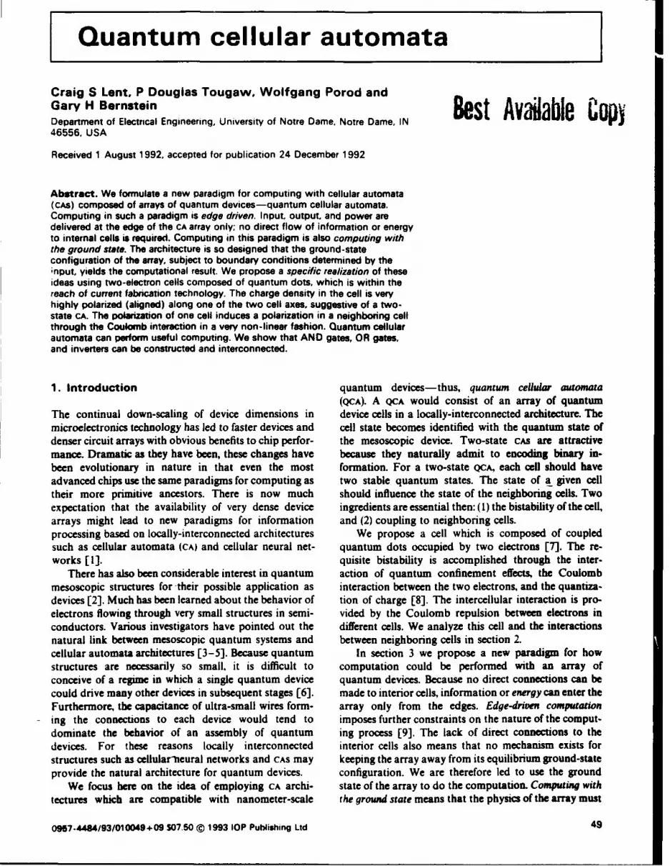
Quantum cellular automata
Craig S Lent, P Douglas Tougaw, Wolfgang Porod andGary H Bernstein Best Avaiable CopyDepartment of Electrical Engineering, University of Notre Dame. Notre Dame. IN46556, USA
Received 1 August 1992, accepted for publication 24 December 1992
Abstract. We formulate a new paradigm for computing with cellular automata(cAs) composed of arrays of quantum devices-quantum cellular automata.Computing in such a paradigm is edge driven. Input, output, and power aredelivered at the edge of the CA array only; no direct flow of information or energyto internal cells is required. Computing in this paradigm is also computing withthe ground state. The architecture is so designed that the ground-stateconfiguration of the array, subject to boundary conditions determined by theinput, yields the computational result. We propose a specific realization of theseideas using two-electron cells composed of quantum dots, which is within thereach of current fabrication technology. The charge density in the cell is veryhighly polarized (aligned) along one of the two cell axes, suggestive of a two-state CA. The polarization of one cell induces a polarization in a neighboring cellthrough the Coulomb interaction in a very non-linear fashion. Quantum cellularautomata can perform useful computing. We show that AND gates, OR gates,and inverters can be constructed and interconnected.
1. Introduction quantum devices-thus, quantum cellular automata(QcA). A QCA would consist of an array of quantum
The continual down-scaling of device dimensions in device cells in a locally-interconnected architecture. Themicroelectronics technology has led to faster devices and cell state becomes identified with the quantum state ofdenser circuit arrays with obvious benefits to chip perfor- the mesoscopic device. Two-state cM are attractivemance. Dramatic as they have been, these changes have because they naturally admit to encoding binary in-been evolutionary in nature in that even the most formation. For a two-state QCA, each cell should haveadvanced chips use the same paradigms for computing as two stable quantum states. The state of a given cell
their more primitive ancestors. There is now much should influence the state of the neighboring cells. Two
expectation that the availability of very dense device ingredients are essential then: (1) the bistability of the cell,arrays might lead to new paradigms for information and (2) coupling to neighboring cells.processing based on locally-interconnected architectures We propose a cell which is composed of coupledsuch as cellular automata (CA) and cellular neural net- quantum dots occupied by two electrons [7]. The re-works [I]. quisite bistability is accomplished through the inter-
There has also been considerable interest in quantum action of quantum confinement effects, the Coulombmesoscopic structures for -their possible application as interaction between the two electrons, and the quantiza-devices [2]. Much has been learned about the behavior of tion of charge [8]. The intercellular interaction is pro-electrons flowing through very small structures in semi- vided by the Coulomb repulsion between electrons inconductors. Various investigators have pointed out the different cells. We analyze this cell and the interactionsnatural link between mesoscopic quantum systems and between neighboring cells in section 2.cellular automata architectures [3-5]. Because quantum In section 3 we propose a new paradigm for howstructures are necessarily so small, it is difficult to computation could be performed with an array ofconceive of a regime in which a single quantum device quantum devices. Because no direct connections can becould drive many other devices in subsequent stages [6]. made to interior cells, information or energy can enter theFurthermore, the capacitance of ultra-small wires form- array only from the edges. Edge-driven computationing the connections to each device would tend to imposes further constraints on the nature of the comput.dominate the behavior of an assembly of quantum ing process [9]. The lack of direct connections to thedevices. For these reasons locally interconnected interior cells also means that no mechanism exists forstructures such as celiularlieural networks and CAS may keeping the array away from its equilibrium ground-stateprovide the natural architecture for quantum devices, configuration. We are therefore led to use the ground
We focus here on the idea of employing CA archi- state of the array to do the computation. Computing withtectures which are compatible with nanometer-scale the ground state means that the physics of the array must
0967-4484/93/010049+09 S07.50 © 1993 lOP Publishing Ltd 49

perform the computation by dissipating energy as it on-site energy for the ith dot is E,,.,. the coupling to therelaxes to the ground state. This has the distinct ad- central dot is t: the charging energy for a single dot is EQ.
vantage that the computing process is independent of The last term represents the Coulombic potential energythe details of the energy relaxation mechanisms and that for two electrons located at sites i and j at positions R,the unavoidable energy dissipation is useful to the corn- and R,. Unless otherwise noted. we will consider the caseputing process. where all the on-site energies are equal. Eo., = E0 .
Section 4 demonstrates that .CAs can perform useful For our standard model cell. on which the numericalfunctions. We show how logical gates and inverters can results reported here are based, we obtain the values ofbe constructed with arrays of the two-electron bistable the parameters in the Hamiltonian from a simple, experi-quantum cell we propose. Section 5 discusses some key mentally reasonable model. We take each site to be aissues in realizing QCAs as a viable technology and section circular quantum dot with diameter D = 10 nm, and take6 identifies technological advantages that a successful E0 to be the ground-state energy of such a dot holding anQCA implementation would enjoy. electron with effective mass m* = 0.067 mo. The near-
neighbor distance between dot centers, a, is taken to be20 nm. The Coulomb coupling strength, V(, is calculated
2. Few-electron quantum cells for a material with a dielectric constant of 10. We takeEQ = VQ/(D/3) and t = 0.3 meV.
The specific cell we consider here is shown in figure 1. It is useful to define a quantity which represents theFour quantum dots are coupled to a central dot by degree to which the charge density for a given eigenstatetunnel barriers. The two electrons tend to occupy anti- of the system is aligned linearly. This alignment could bepodal sites in one of two configurations. shown in the either along the line through sites I and 3 or along thefigure as the P = + I and P = - I configurations. Our line through sites 2 and 4. For each site, we calculate theanalysis below will show that the cell is indeed in one of single particle density pl, which is simply the expectationthese two stable states, and that an electrostatic per- value of the total number operator for the two-electronturbation, perhaps caused by neighboring cells, switches eigenstate. The polarization, P, is defined asthe cell between these two states in a very abrupt andnon-linear way. This permits the encoding of bit in- p I t + P3) -- (i + . (2)formation in the cell. Po + P1 + P2 + P3 + P4
The essential ingredients that produce the bistable For an isolated cell with all on-site energies equal, nosaturation behavior [10] which is so desirable are (1) polarization is preferred. We will see below that per-quantum confinement, (2) Coulomb interaction between turbations due to charges in neighboring cells can resultelectrons, (3) few-electron quantum mechanics, and (4) in a strongly polarized ground state. The polarizationthe discreteness of electronic charge. thus defined is not to be confused with the usual dipole
polarization of a continuous medium. It simply repres-
2.1. A model for the quantum cell ents the degree to which the electrons in the cell arealigned and in which of the two possible directions the
We model the cell shown in figure I using a Hubbard- alignment occurs. For the states of interest here, the celltype Hamiltonian. For the isolated cell, the Hamiltonian has no dipole moment.can be written The interaction of the cell with the surrounding
environment, including other neighboring cells, is con-Hcl = E E.n,.. + O t(a o..tao, + ao.,ta,.o) tained in a second term in the Hamiltonian which we
Swrite as Me" We solve the time independent Schr6din-
+ V Eqn1 t 1 + X V ni.,,nj.,, ger equation for the state of the cell, IjPN>, under the,> j,&.6 oR - Rj1 (1) influence of the neighboring cells:
Here a,.. is the annihilation operator which destroys a (Heel + He,,,)IJPI>) = E.I''.P>. (3)particle at site i Ui = 0. 1,2.3,4) with spin a. The number The spins of the two electrons can be either aligned oroperator for site i and spin a is represented by ni., The anti-aligned, with corresponding changes in the spatial
part of the wavefunction due to the Pauli principle. Wewill restrict our attention to the case of anti-aligned spins
4 Ihere because that is the ground-state configuration; the
spin-aligned case exhibits nearly identical behavior. TheHamiltonian is diagonalized directly in the basis of few-electron states. We calculate single-particle densities, p,,
3 2 from the two-particle ground-state wavefunction I'Io),P=÷i P=-I
Figure 1. The quantum cell consisting of five quantum A= Z < 0JnI..J1 F0 > (4)
dots which are occupied by two electrons. The mutualCoulombic repulsion between the electrons results in and from the densities calculate the resultant polariza-bwtability between the P + 1 and P= -1 states. tion P. equation 12). To maintain charge neutrality, a
50

:\etI vositie cnar .e. 11, U. [t I m lenit|Uc _ I- L_ _.__-,d!"__ICC
,t each site. For the ioiated cell. this na, no cltect .inu I.:ncluded on the on-site eneries. I-,r se'erai ceiis 1n c:,kLs¢cproximity. as will he considered helowa ie maintenance
o1 rerail ,cil charg• neutrailt\ ,•eans Umt ::ie ficr-.,eilular interaction Is due to•k imm...aurIdr0IC. ,,d - . ,*+migher moments ot the c.ii cnare .;,,itriptlhion. i: eFi, pi P,had a net total charge then ciectron, in ., .it aie.periphery or a group or ceils %,ouiu e., nu it rcsponurMostl, to the net charge ki the other ,.-ds,,.
i.(0.•
-(I0. -t).05 0.00 0.05 0.102.2. The cell-cell response function 1,
ro be of use in a (.% architecture. the polarization of onecell must be strongly coupled to the polarization ofneighboring cells. Consider the case of two nearby cells 0.04 -Ishown in the inset to figure 2. Suppose we fix the charge - --"-+ -" " "> 0.02" """/distribution in the right cell. labeled cell 2. We assume . .0 - -
cell 2 has polarization P 2, and that the charge density on -.. -- 1site 0 is negligible ithis means the charge density is 0.00 """
,completely determined by the polarizationi. For a given
polarization of cell 2. we can compute the electrostatic -0.02-
potential at each site in cell 1. This additional potentialenergy is then included in the total cell Hamiltonian. -0.04 -
Thus the perturbing Hamiltonian is -0.10 -0.05 0.00 0.05 0.10
"".-:cell I 2
where Figure 2. The cell-cell response function. Thepolarization of the right cell is fixed and the induced
P polarization in the left cell is calculated. (a) The calculatedI' 7 = (6) polarization of cell 1 as a function of the polarization of
- .*RP . R,.,I cell 2. Note that the range of P, shown is only from -0.1
is the potential at site i in cell m due to the charges in all to 4-0.1. This is because the transition in the inducedpolarization is so abrupt. (b) The first four eigen-energies
other cells k. We denote the position of site i in cell k as of cell 1. The polarization of the lowest two are shownR&.j The total Hamiltonian for cell I is then in (a).
H'" = Hcell + Hce". (7)= + Wmetric will there be no polarization.
The two-electron Schr6dinger equation is solved using iii The polarization ol one cell induces a polarizationthis Hamiltonian for various values of P.. The ground- in its neiqhbor. Figure 2 shows that even a very slight.:ate polarization of cell I. P,. is then computed as polarization will induce nearly complete polarization of a
described in the previous section. neighboring cell. This cell -cell Coulomb coupling pro-Figure 21b) shows the lowest four eigen-energies of vides the mechanism for (A-like behavior. The rapid
cell I as a function of P_. The perturbation rapidly saturation of the cell-cell response function is analogousseparates states of opposite polarization. The excitation to the gain necessary to preserve digital logic levels fromenergy for a completely polarized cell to an excited state stage to stage.of opposite polarization is about 0.8meV for our The abruptness of the cell-cell response function de-standard cell. This corresponds to a temperature of about T he rutns of the cel- cr po nerfunctin9K. igue 2a1 how P1 as funtio ofP. -th cel . pends on the ratio of the dot-to-dot coupling energy, t in9 K . F igu re 2 (a l sho w s P , as a fu n ct io n o f P , -- the cell -- e u t o . t h o l m n r y f r e e t o s ocell response function. A very small polarization in cell 2 equation 0!1. to the Coulomb energy for electrons onceluespcell I to be very small polarized. hisnoe- different sites. The magnitude of the coupling dependscauses one I the very strongly polarized. This non- exponentially on both the distance between the dots andlinear response is the basis of the Q(AS we describe here. the height of the potential barrier between them (11],As the figure shows, the polarization saturates very
quickly. This observation yields two important results: each of which can be adjusted as engineering parameters."Figure 3 shows how the cell - cell response function varies
liI The hipolar saturation means that we can encode hit with t.information using the cell polarization. A cell iN
almost always in a highly polarized state with P -I. 2.3. Self-consistent analysis of several qua.tum celWe define the P = - I state as a bit value of I and theP = - I state as a bit value of 0. Only if the electrostatic In the analysis of the previous two subsections, the two-
environment due to other cells is nearly perfectly sym- electron eigenstates were calculated for a single cell. It is
51
Best Av S",

1.0 -... the two-electron ground-state eigenfunction:
(n!" + = Eol'r). (10)
From the ground-state eigenfunctions we calculate the, - improved single-particle densities.
0.0-.= " (qiPnj.,l~> (11)
"- The improved densities are then used in equation (8) and
- -" "" - the system is iterated until convergence is achieved. Once-1 .0 - '- - the system converges, the many-electron energy, E ., is
-0.10 -0.05 0.00 0.05 0.10 computed from the sum of the cell eigenenergies using theP1 usual Hartree correction term to account for over-
counting of the Coulomb interaction energy betweenFigure 3. The cell-cell response function for various cells:values of the dot-to-dot coupling energy (t in equation(1)). The induced cell polarization P, is plotted as a -- - (12)function of the neighboring cell polarization Pa. The E-j= EkO- V,results are shown for values of the coupling energy, h.1 _.- Rjt = -0.2 (full curve), -0.3 (dotted curve), -0.5 (dashed It should be stressed that the icHA still treats Coulounbic,curve), and -0.7 (dot-dashed curve) meV. Note that the exchange, and correlation effects between electrons in theresponse is shown only for P2 in the range [-0.1, +0.1 same cell exactly. The Hartree mean field approach is
used to treat self-consistently the interaction betweenelectrons in d~ferent cells. Since electrons in different cells
important to note that for the Hamiltonian employed, are physically distinguishable (there beig no wav-these are exact two-particle eigenstates. Exchange and function overlap), the exchange coupling between them iscorrelation effects have been included exactly. This was zero. The Hartree and Hartree-Fock approximationspossible because we could explicitly enumerate all possi- are therefore equivalent in this case.ble two-electron states and diagonalize the Hamiltonian The converged icHA solution will be an (approximate)in this basis set. We want to analyze clusters and arrays eigenstate of the entire system. In general however, itof cells to investigate possible device architectures. To do need not be the ground state. As with the usual Hartreeso we need to calculate the ground-state wavefunction of approximation, which of the eigenstates the schemea group of cells. Exact diagonalization methods are then converges to is determined by the choice of the initialno longer tractable because the number of possible guess. To find the ground state we must try many initialmany-electron states increases so rapidly as the number state guesses and determine which converged solutionof electrons increases. We must therefore turn to an has the lowest energy. Typically, this does not present aapproximate technique. serious problem for the type of cellular arrays considered
The potential at each site of a given cell depends on here because the set of likely ground states is easilythe charge density at each site of all other cells. We will discerned. In general, a systematic search may betreat the charge in all other cells as the generator of a required.Hartree-type potential and solve iteratively for the self- The procedure described above uses, at each stage ofconsistent solution in all cells. This approximation, the iteration, only the ground-state wavefunction of eachwhich we call the intercellular Hartree approximation cell. If all the excited states of the entire system were(icHAL), can be stated formally as follows. Let 1P'Y be the desired, we would have to include states composed oftwo-electron ground-state wavefunction for cell k, and p,' excited cell states as well. Since our interest is in thebe the single-particle density at site j in cell m. We begin ground state, this is not necessary. It is relevant to pointwith an initial guess for the densities. Then, for each cell out however, that because each cell is in a 'local' groundwe calculate the potential due to charges in all other cells, state, we do not require coherence of the many-electron
wavefunction across the whole array of cells. All that is= i V - (8) required to support this analysis is that the wavefuanction
1 jR,.j - R,.,I, is coherent across a single cell. No information about the
Although the neighboring cells will normally dominate phase of the wavefunction in other cells is relevant to the
this sum, we do not examine only near-neighbors but wavefunction in a given cell-only the charge densities in
include the effect of all other cells. For each cell k, this other cells need be known.
results in a perturbation of the basic cell Hamiltonian ofequation (I I 3. Computing with quantum cellular automata
M alli Vn,.,. (9) We present a new paradigm for computing with QcA.I-Relg Ce This represents a complete picture of how quantum
The Schr•dinpr equation for each cell is now solved for devices could be coupled in a CA architecture to perform
52

aseful functions. rhe parauinm Ae propose i •nown .arrav is no ronger in the ground state but is nou in anschematically in fieure 4 %%e %%ill focus on the 7ero- cxcited non-stationary state for the new boundary con-temperature case: temperature effects ,ii1 be considered ditions. In the time between 0 and t,. a charactenstic,helow. As shown in the figure. the inputs are along an relaxation time. ýaraous dissipative processes will bnng,:dge of the arras Specilun_ the inputs .onsists ofi the arra, to its new ground-state configuration. After-lectrostatically fixing the poiarization of the input cells. tihat. the array %6il he stable until the boundary con-This could be accomplished by simply applying voltages ditions are changed again. During the relaxation time theto conducting 'set lines which come in close proximity to temporal evolution of the system is terv complicated.the cells, but any method that fixes the cell polarization Even %kithout dissipation. the system will undergo,tate would do. The output cells are not fixed: their quantum oscillations due to interference between thepolarization state is sensed. perhaps hv electrostatic %arious eigenstates which compose the t = O state. The,:oupling to 'sense" lines. There could also he several input dissipative processes. like phonon emission, introduceand output edges. Computation proceeds in the follow- extraordinary complication in the temporal evoluuon.ing steps: The exact state of the system at a particular time t < t,
Ii) Write the input bits by tixing the polarization state depends not just on phonon emission rates, but on theof cellsalong the input edge edfingthed oarientcomutatioe particular phonons emitted by these particular electrons.
of cells along the input edge iedge-driven computation). In short, the temporal evolution before t = tr depends on(ii) Allow the array to relax to its ground state with the precise microscopic details of the dissipative
these inputs (computing with the ground state). dynamics. By contrast, the ground state configuration toiiiii) Read the results of the computation by sensing which the system relaxes is completely independent of the
the polarization state of cells at the output edge. dissipation mechanisms. Hence we choose to use the
The essential elements that define this computing para- ground state only for computing.digm are computinq with the around state and edqe-drivencomputation, which we discuss below. 3.2 Edge-dive computation
3.1. CIn the OCA computing paradigm we are proposing, theinput data is represented by edge cells whose polarization
The advantage of computing with the ground state is that is fixed. Computing then proceeds by allowing theit leaves the computing process insensitive to the details physics interior to the QCA to 'solve' the dissipative many-of the dissipative processes which couple the electrons in electron problem for this new set of boundary conditions.the array to the environment. Consider a QCA at zero The array is designed so the part of the ground-statetemperature for which all the input cells have been held "solution' of the many-body problem which appears atin a fixed state. Dissipative processes have brought the the output edge corresponds to the solution of thearray to its ground-state configuration for these bound- computing problem posed by the input data.ary conditions. Suppose at time t = 0 the input cell states The advantage of writing input and reading outputare set to their new input values completely abruptly. only at the edges of the array is that no separateJust after the inputs are applied at the edge of the QCA, the connections to the array interior need be made. Because
quantum devices are of necessity extremely small, theproblem of making contacts to each element or device
Inputs Outputs becomes severe. If a single array contains thousands ofindividual cells, the 'wiring' problem is overwhelming.
Edge-driven computation is, in fact, the practicalrequirement which makes computing with the groundstate necessary. If no connections can be made to theinterior of the array. there is no controlled mechanism for
a) keeping the system away from the ground state. Neitherclocking nor refresh mechanisms are available. With achange in input, the system will dissipate energy and finda new equilibrium ground state. The only choice is
Set Sense whether to try to perform computation with the system'sSm transient response. or with its ground state. For the
b) reasons discussed above, the ground-state approach ispreferable.
Figure 4. The new paradigm for computing with Conventional computing, by contrast, is done usingquantum cellular automata (OCAs). The input to the OCA Is very highly-excited. non-equilibrium states. Because eachprovided at an edge by setting the polarization state of the element ldevicel can be separately contacted, energy canedge cells (edge-drven computation), The QCA is allowed be fed into the system at each point. The entire systemto dissipatively move to its new ground-stateconfiguration and the output is sensed at the other edge can thereby be maintained in non-equilibrium states. The
(computing with the ground state). The 'set' and 'sense' advantage of this is that the energy difference between thel•nes are shown schematically. states used for computing can be very much larger than
53
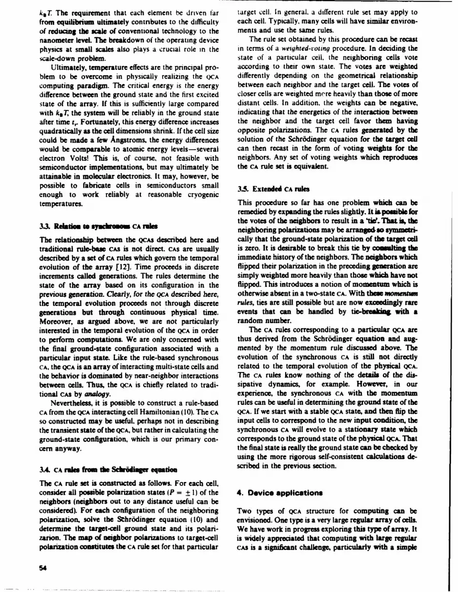
k*T The requirement that each element be driven far target cell. In general. a different rule set may apply tofrom equilibrium ultimately contrbutes to the difficulty each cell. Typically, many cells will have similar environ-of reducing the scale of conventional technology to the ments and use the same rules.nanometer level. The breakdown of the operating device The rule set obtained by this procedure can be recastphysics at small scales also plays a crucial role in the in terms of a weighted-toting procedure. In deciding thescale-down problem. state of a particular cell. the neighboring cells vote
Ultimately, temperature effects are the principal pro- according to their own state. The votes are weightedblem to be overcome in physically realizing the QCA differently depending on the geometrical relationshipcomputing paradigm. The critical energy is the energy between each neighbor and the target cell. The votes ofdifference between the ground state and the first excited closer cells are weighted mere heavily than those of morestate of the array. If this is sufficiently large compared distant cells. In addition, the weights can be negative,with ksT, the system will be reliably in the ground state indicating that the energetics of the interaction betweenafter time t, Fortunately, this energy difference increases the neighbor and the target cell favor them havingquadratically as the cell dimensions shrink. If the cell size opposite polarizations. The CA rules generated by thecould be made a few Angstroms, the energy differences solution of the Schr6dinger equation for the target cellwould be comparable to atomic energy levels-several can then recast in the form of voting weights for theelectron Volts! This is, of course, not feasible with neighbors. Any set of voting weights which reproducessemiconductor implementations, but may ultimately be the CA rule set is equivalent.attainable in molecular electronics. It may, however, bepossible to fabricate cells in semiconductors small 3.5. Extended CA rulesenough to work reliably at reasonable cryogenictemperatures. This procedure so far has one problem which can be
remedied by expanding the rules slightly. It ispossible forthe votes of the neighbors to result in a tie. That is, the
3.3. Rei . W ajuzekawom CA ries neighboring polarizations may be arranged so symmeri-The relationship between the QCAS described here and cally that the ground-state polarization of the target celltraditional rule-base CAS is not direct. CAS are usually is zero. It is desirable to break this tie by consulting thedescribed by a set of CA rules which govern the temporal immediate history of the neighbors. The neighbors whichevolution of the array [12]. Time proceeds in discrete flipped their polarization in the preceding generation areincrements called generations. The rules determine the simply weighted more heavily than those which have notstate of the array based on its configuration in the flipped. This introduces a notion of momentum which isprevious generation. Clearly, for the QCA described here, otherwise absent in a two-state CA. With then momentumthe temporal evolution proceeds not through discrete rules, ties are still possible but are now exceedingly raregenerations but through continuous physical time. events that can be handled by tie-breakial with aMoreover, as argued above, we are not particularly random number.interested in the temporal evolution of the QCA in order The CA rules corresponding to a particular QCA areto perform computations. We are only concerned with thus derived from the Schr6dinger equation and aug-the final ground-state configuration associated with a mented by the momentum rule discussed above. Theparticular input state. Like the rule-based synchronous evolution of the synchronous CA is still not directlyCA, the QCA is an array of interacting multi-state cells and related to the temporal evolution of the physical QCA.the behavior is dominated by near-neighbor interactions The CA rules know nothing of the details of the dis-between cells. Thus, the QCA is chiefly related to tradi- sipative dynamics, for example. However, in ourtional cAs by analogy, experience, the synchronous CA with the momentum
Nevertheless, it is possible to construct a rule-based rules can be useful in determining the ground state of theCA from the QCA interacting cell Hamiltonian (10). The CA QCA. If we start with a stable QCA state, and then flip theso constructed may be useful, perhaps not in describing input cells to correspond to the new input condition, thethe transient state of the QCA, but rather in calculating the synchronous CA will evolve to a stationary state whichground-state configuration, which is our primary con- corresponds to the ground state of the physical QCA. Thatcern anyway. the final state is really the ground state can be checked by
using the more rigorous self-consistent calculations de-
3.4. CA rides from the Scbrbgequation scribed in the previous section.
The CA rule set is constructed as follows. For each cell,consider all possible polarization states (P = + 1) of the 4. Device applicationsneighbors (neighbors out to any distance useful can beconsidered). For each configuration of the neighboring Two types of OCA structure for computing can bepolarization, solve the Schrddinger equation (10) and envisioned. One type is a very large regular array of cells.determine the target-cell ground state and its polari- We have work in progress exploring this type of array. Itzarion. The map of neighbor polarizations to target-cell is widely appreciated that computing with large regularpolarization constitutes the CA rule set for that particular cAs is a significant challenge, particularly with a simple
54

rule set. The solution to this difficult probiem ma' have W . -
the greatest long-term potential. however. for exploiting *' L. Lithe massive parallelism inherent in the QWA paradigm. 0
A second type of QCA structure involves a highly
irregular array of cells. We show below that using simple Figure 6. An inverter constructed from a quantum cell
irregular arrays one can produce structures analogous to automatonwires. inverters, AND gates and OR gates. Since these
can be connected together. more complex devices such as ,ort of fan-out is appropriate for the edge-driven para-
adders and multipliers can be constructed. Because the digm discussed above.
individual devices are so small, this represents a potent-ially enormous increase in functional density in anarchitecture free of the usual interconnect problems. We
examine below how these basic logical gates can be By offsetting one chain of cells from another, as shown inconstructed from quantum cells. figure 6. an inverter can be constructed. If the polariza-
The device configurations shown are the results of tion of the one end is fixed, the polarization of the otherself-consistent calculations of the ground state using the end will be opposite.
ICHA described above. Figure 5 shows the calculatedground-state charge density on each site of the cellular 43. AND and OR gatesarray. In these figures the dot diameters reflect the
relative electron density at each site (dot) in the cell. AND and OR gates can be made from the intersection oftwo wires. Figure 7 shows an OR gate. The darker boxes
4.1. Wires are around the input cells. Their polarization is set tocorrespond to the logical values shown. For the case
A linear chain of cells oriented as shown in figure 5(a) when the inputs are 0 and I (figure 7(c)), the central cell
functions as a wire, transmitting a 0 or I (P = -t- I or state would normally be indeterminate since a 'tie vote'
P = - 1) from one end of the wire to the other. This is exists between the input cells. To resolve, this we bias thedemonstrated by fixing the polarization of one end (the central cell by increasing the site energy on sites 2 and 4
left in the figure), while letting the other end be uncon- slightly. This could be accomplished by making the
strained, and calculating the self-consistent ground state quantum dot diameter slightly smaller on these two sites.
of the chain using the ICHA method. Figure (5a) shows the It is then slightly more energetically favorable for the cell
results of this calculation. Not surprisingly, the ground to be in a 1 state, thus breaking the tie. The AND gate isstate consists of all cells aligned with the same polariza- constructed in exactly the same way except that the
tion as the end cell. The first excited state of the chain has central cell is biased toward the 0 state. The AND gate is
a 'kink' in it at the chain center, i.e., half the cells shown in figure 8. Both these figures reflect the results ofpolarized one way and half polarized the other. For our self-consistent solutions of the many-electron problem
example, the energy of the first excited state is about for the entire array shown.I meV (AE/kT = 10 K) above the ground-state energy.Wire bends and fan-out are also possible. as shown in 44. Memory cell
figure 5(b) and (c), respectively. Again, the left-hand cell isfixed and the ground-state configuration calculated. This A single quantum cell can act as a memory storage cell.
Once prepared in an eigenstate with P = + 1, for
a) a)b) 0
1 OE]_
b) C)0) E
Figure 5. OCA wires: (a) the basic wire; (b) a corner in a 71177wire; (c) fan-out of one signal into two channels. In each L?- L
case the darker (left-hand) cell has a fixed polarizationwhich constitutes the input. Note that these figures are Fnot simply schematic, but are a plot of the results of aself-consistent many-body calculation of the ground state Figure 7. An OR gate. The cells in darker squares arefor the cellular array. The diameter of each circle is fixed to the input states. The cell in the dashed square isproportional to the calculated charge density at each site. biased slightly toward the '1' state.
55

a) 1F b) 0 rl realizing a QCA structure. Any implementation must dealwith several issues of key importance to the successful
' i •operation of the cell we have described.
5.1. Uniformity of cell occupancyE] It is important for the operation of the QCA that each cell
contain two electrons. The cell-cell response functiondegrades significantly of one or three electrons are in a
c , cell. Fortunately, the physics of the cell acts to ensure thatS0 the occupancy will be very uniform. This is so because the
LL_ Coulomb interaction causes significant energy-level7 splitting between the different cell charge states. The
I r."'J Coulomb energy cost to add the third electron is on theorder of 10meV for cells with a 3Onm separation.
Figure &. An AND gate. The cells in darker squares are Experiments by Meurer et al [13] have shown thatfixed to the input states. The cell in the dashed square is uniformity in the number of electrons per dot can bebiased slightly toward the "0' state. maintained in arrays of 108 dots.
example, the cell will in principle remain in that con-figuration indefinitely. One problem is that slight variat- 5.2. Dot size controlions in the potential environment may make it slip into The size of the fabricated quantum dots must be fairlythe other eigenstates. To avoid this it may be desirable to well controlled. Variations in the size of the dots translateuse small or medium-size arrays of quantum cells to store into variations in the confinement energies on each dot.each bit. This is shown schematically in figure 9. One To car ito o b the Coulomb inter-advntae o a eguarrecanglararry f cllsis hatit The cell bistability occurs because the Coulomb inter-advantage of a regular rectangular array of cells is that it action is determinative in selecting a preferred polariza-may be possible to use the interaction of many cell with tion state. If the magnitude of the variation among thethe set and sense lines (the exact mechanism for setting tiandsesin i no citialher).The problem of making dots in the confinement energies is greater than theand sensing is not critical here). nof-t aing Coulomb energies involved, the cell will be pinned at anon-interfering address lines is certainly non-trivial, fixed polarization. Note that dot size variations are
critical only within a single cell; variations between
5. Issues for OCA 88 a technology different cells are easily tolerated.
Fabrication of QcAs in semiconductors appears to be 5.3. Temperaturewithin reach of current technology. The GaAs/AIGaAs
withn rachof crret tchnoogy Th Ga~/Ala~s The temperature of operation is a major factaTh Our QCAsystem has proven fruitful as a means of fabricating quantumpell is opectio wor ator.qui hluquantum dot structures by imposing electrostatically a quantum cell is expected to work at liquid heliumpattern on the two-dimensional electron gas formed at temperatures for dot dimensions which are within thethe heterojunction interface. Other materials systems, capability of current semiconductor fabrication tech-including molecular systems, are also candidates for nology. As technology advances to smaller and smallerdimensions on the few-nanometer scale, the temperatureof operation will be allowed to increase. Perhaps our
a) b) envisioned QCA will find its first room temperatureimplementation in molecular electronics.
+ + + + 6. Technological benefits
+ + + + If successful, ocAs would represent a revolutionary,+ + + + + rather than evolutionary, departure from conventional
+ + + + + electronics. In this section we review some possiblebenefits a QCA technology might provide.
+ + + + + Quantum cellula automata solve the interconnection
0 + + + + + problem. It is widely acknowledgcd that the main chal-S+~ +e lenge to further improvements in microelectronics is the
interconnection and wiring problem. The QcAs we dis-Figure 9. Quantum cellular arrays as memory storagecells. A single bit can be stored in (a) a single cell, (b) aline of calls, or (c) an array of cells. Arrays of cells would Interconnect lines are no longer necessary to provide themake the storage more robust. communication between cells; the Coulomb interaction
56

provides the coupling mechanism. Edge-driven corn- Nense defined above) ground states. The response of thisputation requires neither energy nor information to be polarization to the electrostatic environment is highlytransmitted directly to interior cells. Computing with the non-linear and exhibits the bistable saturation necessaryground state makes both clocking and refresh signals for a two-state CA. The concept of edge-driven corn-unnecessary. putaton solves the interconnection problem. The concept
Quantum cellular automata make possible ultra-high- of computing with the ground state in the QCA approachdensity computing elements. The chief technological ad- permits ultra-fast operation, eliminates problems of in-'antage of the proposed structures is the improved terconnect delays, resistive and capacitive effects, powerfunctional density of computing elements. With a 10 nm dissipation. and limited densities associated with con-design rule. the cell dimensions would be about ventional architectures.50 nm x 50 nm, which translates into an extremely highpacking density of about 1010 cells cm - 1. Since, as shownabove, a single cell can function as a logical gate, this Acknowledgmentsrepresents an extremely high functional density.
Quantum cellular automata are extremely low in power This work was supported in part by the Air Force Officedissipation. High packing density is usually accom- of Scientific Research and the Office of Naval Research.panied by high power dissipation. However, in QCA This material is based upon work supported under astructures, the information is stored in physical systems National Science Foundation Graduate Fellowship.
close to their ground state. The energy input to the arrayis the energy required to set each input bit-about I meVper input bit. This energy is dissipated in the time it takes Referencesfor the QCA to relax to its new ground-state configuration,probably less than a few picoseconds (phonon scattering [1] Ferry D K, Akers L A and Greeneich E W 1988 Ultratimes). This represents a power dissipation of roughly Large Scale Interconnected MiToekca
(Englewood Cliffs, NJ: Prentice Hall)10- o W per input bit, much less than conventional [2] For a recent overview see Kirk W P and Reed M Adevices. (ed) 1992 Nanostructures and Meswopic System.
Quantum cellular automata offer the possibility of (Boston: Academic)ultra-fast computing. As estimated above, the computa- [3] Bate R T 1977 Bull. Am. Phys. Soc. 22 407tion occurs in a QCA over the relaxation time for the [4] Randall J N, Reed M A and Frazier G A 1989 J. Vac.
Sci. Technol. B7 1398electrons in the array, probably on the order of picosec- [5] Ferry D K, Barker J R and Jacoboni C (ed) 1991onds. It is clear that this relaxation time is a function of Granular Nanoelectronics (New York: Plenum)the electron-phonon coupling and represents a funda- [6] Landauer R 1989 Phys. Today 42 119mental speed limit for computation with electrons in a [7] A proposal for cells with single-electron occupancy hassemiconductor. been made, but lacks the requisite bistable
character. See Bakshi P, Broido D A and Kemps KQuantum cellular automata may facilitate fabrication 1991 J. Appi. Phys. 70 5150
qf ultra-dense memory storage. The QCA cell encodes a bit [8] Lent C S, Tougaw P D and Porod W 1993 Appl. Phys.of information. Writing and reading the bit involves very Lett. 62 714low power dissipation and is very fast. While problems of [9] The edge-driven paradigm proposed here is to becell addressing and cell volatility appear challenging, the distinguished from conventional systolic
possibility of solid-state electronic storage of information architectures. In systolic arrays information is inputonly at the edges, but energy must be separately fed
at these densities invites further investigation, to each computational element typically through
power lines to each cell. In the paradigm discussedhere, both energy and information are supplied only
7. Summary to the edge cells.[10] Obermayer K, Mahler G and Haken H 1987 Phys. Rev.
Lett. 53 1792We have presented a specific model for using nanoelec- [11] A one-dimensional treatment is given at length intronic devices in a cellular automata architecture and Morrison M, Estle T and Lane N 1976 Quantumproposed a new paradigm for computing in this frame- States of Atoms, Molecules, and Solids (Englewoodwork. Each cell consists of a central quantum dot and Cliffs, NJ: Prentice-Hall) ch 13
four neighboring dots occupied by two electrons. The [12] Toffoli T and Margolus N 1987 Cellular AutomataMachines: A New Environment for Modeling
Coulomb repulsion between the two electrons, quantum (Cambridge, MA: MIT Press)confinement effects, and the discreteness of the electronic [13] Meurer B, Heitmann D and Ploog K 1992 Phys. Rev.charge, combine to produce strongly polarized (in the Le:i. 68 1371
57

A novel quantum wire formed by lateral p-n-p junctions betweenquasi-two-dimensional electron and hole systems at corrugatedGaAs/AIGaAs Interfaces
Henry K. Harbury and Wolfgang PorodDepartment of Electrtca Engineering, Lnwernltv of Notre Dame, Aozre Dame. Indiana 46556
Stephen M. GoodnickDepartment of Electrcal and Computer Engineering, Oregon State Unwerstav. Corvadlh. Oregon 97331
(Received 6 August 1992. accepted for publication 19 October 1992)
Numerical modeling of a novel quantum wire structure formed by the confinement of electronsbetween lateral quasi-two-dimensional (Q2-D) p-n junctions in a corrupted GaAs/AIGaAsheterostructure is reported on. Such a quantum wire may be realized at the tip of a Si-dopedAIGaAs overgrown V groove in a SI-GaAs substrate due to the surface orientation dependenceof Si doping. The two-dimensional conduction and valence band potential profiles for theelectron and hole charge densities are solved within a senuclassical Thomas-Fermi screeningmodel. The quantized electronic wire states at the heterointerface are then obtained by solvingthe two-dimensional effective mass Schrddinger equation using the calculated potential profile.The parameter space of the one-dimensional electron system is explored to establish whichfeatures of the structure are dominant factors in controlling the electronic states. It isdemonstrated that the energy level spacing of the quantum wire depends primarily on the lateralconfinement width in the n-type region at the tip of the V groove. The ground state energy of thewire is shown to depend on both the lateral confinement width and the vertical heterointerfaceconfinement width. The results of our initial calculations are also reported on to incorporatelateral gates on the surface to obtain direct control of the quantum wire transport properties.The advantages of fabricating quantum wires with this structure compared to conventionalmethods of electrostatic confinement are discussed.
I. INTRODUCTION hole gas systems (2DEG and 2DHG, respectively) with
Recent experiments have demonstrated that Si behaves Si-doping densities in excess of 5 X 1017 cm-3.
as a substrate orientation dependent amphoteric dopant in A variety of novel complementary device structures
molecular beam epitaxial (MBE) grown GaAs and Al- may be based on lateral p-n junctions f.,rmed between high
GaAs. This effect was first studied on As-terminated {I I I} mobility 2DEG and 2DHG systems. In particular, exploit-and { 110) planes;1 then further studies were reported on ing the amphoteric dopant behavior of Si in a selectivelyGa-terminated (111}A, As-terminated {111}B, {100), etched and epitaxially regrown V groove structure presents(211 }, and higher index planes.' 3 These studies show that. a novel quantum wire system realized between lateral p-nunder suitable growth conditions, Si-doped overlayers junctions.7 The depletion regions in such a HEMT-grown on { 1001 GaAs substrate surfaces have donor be- compatible p-n-p-type geometry provide lateral confine-havior, whereas Si-doped overlayers grown on Ga- ment of the carriers at the heterointerface of the n-typeterminated { Ill }A GaAs substrate surfaces have acceptor center region, thereby realizing a quantum wire. The use ofbehavior. " junctions for lateral confinement of quantum wires was
The controllable amphoteric nature of Si doping inr pioneered by Dean and Peppers and by Fowler and co-cited the investigation of fabricating lateral ,on junctions workers. 9 P-groove geometries have been previouslF-cax-in GaAs. Bulk GaAs lateral p-n junctions with good diode plored for the design of quantum wires. 1-13 This new de-current-voltage characteristics were reported by Miller in19g5. HEMT-opaible hetertructure lateral p-n junc si, however, may offer some advantages compared to
tions. between quasi-two-dimensional electron and hole present unipolar structures,1 4 which use metal gate electro-systems, were reported by Ebner et aL in 1990o. In this static confinement or sidewall etching.
latter study, Si-doped Al0 3Ga0.7As was epitaxially re1rown In this paper we report on numerical modeling of the
on a semi-insulating corrugated GaAs substrate. The selec- lateral p-n-p quantum wire system realized in a corrugated
tively etched and epitaxially regrown structure was fabri- GaAs/AIGaAs heterostructure. In Sec. II we present our
cated with exposed Ga-terminated {I Il }A facets on the model of the system, and in Sec. III we discuss our solutionnormally exposed { 100} substrate. Ebner et aL5 reported methods for obtaining the two-dimensional electrostaticelectroluminescence results that correspond to the GaAs potential for electrons and holes, and the electronic statesquantum well bead gap of such a system. and Harbury of the quantum wire. We also present the details of theet aL6 reported calculations that confirm the existence of a numerical method in the Appendix. Our results are pre-lateral p-n junction between two-dmensonal electron and sented in Sec. IV, and we conclude in Sec. V.
10w J. Am* Phys, 3 3(3). 1 Fsibmy I99M 0021-8979/93/031509-12506.00 D 1993 AmnincI InsU-s of Phi 1500
1001 1 - Doped A ia -.& 1001 2k. Tm JVi r) =4171
n ivipW n' %.,•/ -tvpe 50 nm -
_DEG _ ,'. DFt;
0 1001 -( [E-E(r I/kofl'1'dE/kBT)-P- I -exp((E E
SIDEGii •.~ !i
-= W ire :• i • ; i ! i -ý'• = V F l 17 ), (2 )
where .V = 2(2-,rk8 Tm*1/h2 )< , :s the effective conduction
band density of states. 7=I(EF-E.(r))/k9T measures theSI GaAs Substrate separation between the Fermi level. EF, and the position-
dependent conduction band edge, E,(r), and F,/ 2(17) is theFermi-Dirac integral of order 1/2. A similar term is ob-tained for the hole density, p(r) =,N,F,1 2 ( 17), where 71is
FIG. I. Schematic diagram of the model V-groove corrugated hetero- now the separation between the valence band edge and theStructure geometry. The n-type or p-type nature of the amphotenc silicon Fermi level, and N, is the effective valence band density ofdoped overlayer is labeled along with the corresponding crystallographic-urface onentation. Possible formation of 2DEG's. 2DHG's. and a I DEG states..s also noted. The hatched region represents the computation domain. We enforce bulk charge neutrality deep inside the
semi-insulating GaAs substrate, assumed to be slightly ntype with a background doping density of 1.OX 1015 cm- 3
which is completely ionized. A density of surface states
II. MODEL SYSTEM along the {100} and {I11} exposed facets is also assumed,such that the electrostatic potential is pinned to the near
Figure 1 shows a schematic diagram of the model cor- midgap value of 0.8 eV separation between the conductionrugated GaAs/AIGaAs heterojunction system. The chosen band edge and the Fermi level. The problem domain ex-
overlayer thickness and composition are similar to those of tends far enough from the p-n junction regions such that
a lateral light emitting structure fabricated by Ebner et at. 5 the electrostatic potential becomes invariant parallel to thea laeralligh emitingheterointerface.
A 50 nm thick layer of Si-doped Al0 3Ga 0o7As is overgrown he oine d e h p u
on an etched V groove of a semi-insulating GaAs substrate. The confined states of the p--n-p quantum wire struc-
The sidewalls of the V-groove expose the {I 1I IA family of ture are also of interest. The bound state wave functions
planes of the normally {100} terminated substrate. As in- are sought by solving the two-dimensional Schr6dinger
dicated in Fig. 1, the amphoteric Si-doped overlayer exhib- equation for a computed potential profile,
its n-type behavior on the { 100} surfaces and p-type be- hihavior on the {1l1}A surfaces. The two-dimensional -_,MV 2ib(r)+[V(r)-e,6(r)]40(r)=E0b(r). (3)electron and hole gas shown in Fig. I (labeled 2DEG and ,"DHG. respectively) forms along the heterointerface for Here, V(r) includes external potentials and band offsetssuitable doping conditions. and d(r) is the electrostatic potential obtained from the
The hatched region in Fig. I represents the finite ele- solution of Poisson's equation for the V-groove geometry.ment calculation domain used to model the p-n-p quan- The decay of the wave function far from the potentialtum wire structures. The range of the ternary composition, .pocket" that forms the quantum wire provides the neces-the doping density, and the structural dimensions are the sary boundary conditions to formulate Eq. (3) as anparameters that define the system. A two-dimensional eigenvalue/vector problem. The wave functions of interest,equilibrium potential profile of the model geometry is however, are the lowest energy quantum wire states. Thesought for different material parameters. The band bending problem, therefore, can be reduced to a subspecie of the fulldue to the electrostatic potential, 4)(r), is obtained from the eigensystem.solution of Poisson's equation within a semiclassicalThomas-Fernu screening model.
e Ill. NUMERICAL METHODS
Vh(r) = -o(n(r)-p(r)+Nj-NV). (1) The solution of the two-dimensional Poisson and
Schrodinger equations is a challenging numerical problemComplete ionization of the impurities is assumed at room that requires domains of highly nonuniform mesh design,temperature. such that the background doping of the semi- bandwidth optimization, and sparse matrix methods. Theinsulating GaAs, assumed to be lightly n type, contributes general considerations of the solution method are discussedto N ý in the substrate, and the amphoteric Si doping con- in Sec. III A, whereas the details of the numerical methodtributes to both N- and N' in the overlayer region. The are deferred to the Appendix. The interestng and oftenelectron denmity, n(r), is given by the Fermi-Dirac integral ignored subject of nonuniform mesh generation is dis-of order -, " cussed in Sec. III B.
1510 J. Appl. PFt. Vol. 73, No. 3, 1 Fe•uAry 1993 Hatury, PorN, alnd GoaWig 1510

- i) nm
lU- hi rd-- 00 nrn\,7
-* -- 15 0nm
- 175 '0 nm°"- • 20 --•rn
0150 nm
.0 !75 M,.10 -ZO unm
0 4 5 6 7 9 9 0 I 12 -300m"Itwto = Nmber to/
0 0 :0 .O 0 •040 6O 70 so
FIG. 2. Convergece of the Poisson solution Newton-R~aphson iteration Iteration Number
scheme for several different p-n-p geometries.FIG. 3. Convergence of the Schrodinger solution subspe iteratioscheme for several different p-n-p geometries.
A. The solution of Poisson and Schrodinger equations
The two-dimensional Poisson and Schrddinger equa- 12 iterations with a typical cumulative solution time of 430tions are both solved with the finite element method. The sec on an IBM RISC System/6000.Poisson equation is solved for the discretization domain For the Schrodinger equation. the asymptotc decay ofschematically shown by the hatched region in Fig. 1, the wave function can be modeled by either zero-valuedwhereas the Schr6dinger equation is only solved for the Neumann boundary conditions or zero-valued Dirichietsmall subregion near the V-groove tip, where the electro- boundary conditions. Continuity of the wave functionstatic potential "pocket" defines the quantum wire. across the heterointerface is implemented with the penalty
For the Poisson solution, the bulk charge neutrality element method and provides compatibility with the Pois-boundary conditions deep inside the GaAs substrate are son solver. The details of the finite element formulation ofimplemented by fixing the electrostatic potential at a few the Schr6dinger equation are deferred to Appendix B.points on the boundary to the value consistent with the Because only the lowest few eigenstates are sought, thebackground doping, and by applying zero-valued Neu- discretized Schridinger equation is solved by a sub• ecemann conditions on the remainder of the bulk boundary. iteration method. Efficient skyline storage and spurne ma-This condition forces the boundary normal electric field to trix methods are used to obtain the lowest ten bound states.zero. and forces the potential to the proper equilibrium The iterative error of the subspace algorithm is plotted inbulk value. Surface pinning on the exposed facets is imple- Fig. 3 for the ground state of the lateral p-"-p quantummented by Dirichlet conditions, which force the conduc- wire for the same selection of n-region V-groove tip widths.tion band potential to the approximate midgap value of 0.8 as were chosen for Fig. 2. After initial oscillation, the erroreV above the Fermi level. Zero-valued Neumann boundary exponentially decreases at approximately one decade everyconditions are applied along the side boundaries to model 15 iterations. For the finite element Schrodinger domainthe asymptotic invariance parallel to the heterointerface. consisting of 3482 elements and 1876 bandwidth-optimizedThe discontinuty in the electrostatic potential at the het- nodes, a solution of a 20 eigenstate subspace over 120 it-erointerface is treated as a linear constraint on the system erations typically consumes 240 cpu seconds on an IBMof equations and is implemented with the penalty element RISC System/6000.method. The nonlinear Poisson equation is linearized bythe Newton-Raphson iterative method. The details of thefinite element formulation and linearization are deferred toAppendix A. Two-dimensional numerical modeling of realistic
The resulting system of linear equations is solved by structures, such as those considered in this work, requiresstandard LIU decomposition, backward substitution, and the development of sophisticated mesh domains. Bulkforward elimination. Bandwidth optimization of the dis- charge neutrality boundary conditions imply that the do-cretized equation numbers in conjunction with the skyline main, fl, must extend microns into the bulk region. At thestorage technique provide an efficient solution of the linear heterointerface and in the p-n junction depletion regions,system. The iterative error-of the Newton-Raphson solu- however, the potential profile may undergo large variationstion is plotted in Fig. 2 for typical runs of the lateral p-n-p in nanometer distances. The disparity between character-quantum wire domain for various widths of the n-type istic length scales and the need to keep the problem sizeregion at the V-groove tip. The finite element domain con- computationally tractable constrams the discretizationsists of 16 168 elements and 8427 bandwidth-optimized scheme to highly nonuniform mesh designm. A further con-nodes. The error drops by approximately 9 decades within straint on mesh design is the need to preseve the charac-
1511 J. AL. Pt. VoL 73, No. 3. 1 Pkumwy 1993 HwuiLy, Poa r. wdGoantt 1511

1221
FIG 4 Songiwsiori. tringmhr, eigiewft m.sh domain iieiaw to ve theSchrodinger equatioa for the quentugm *ire state- The Schrodinigt meshn4
Na smahi ¶thbdomma of the Poationa mesh cut tramn the re" oti0 thepomteitas -pockeci fored at the bottom of the & groov~e ibis mink has 5 ývwSi w~482 tnntruiar to im ad 1876 nodima5 4 - 2
.ý4)h.5 411 1'4 -'5 i 1 :V 373 Soo 231 750
rensine geometry of the structure. The 54 'r angle between FIG 5 and d.itre for the Watergii p-*.-p quamm mie -nnthe f l00} and (I I I I crystallographic planes. for example. sbo are the codonandv' begi siong t~ hInamust be maintained throughout the domain. !or a loo nm ions centerV .ttvpe sectionl and a Si-4oping myI of 1 0
With a rectangular master element design. it would be lO 10m The irmtis how tront a&W %de v1w" of the two-doinmmnlt
difficult to maintain arbitrary angles throughout the do- tiodiatawag bend proSile fli pomenaiii -pocket' th hub tdiEumeWWTis Ais ado mald.
main. and the resulting system of equacions would likely beintractably large. With the triangular master clement. how-ever. it is easy to maintain arbitrary geometric angles in net the sudniusi together. The special penmy elimsefnonuniform mesh desigs. Furthermore standard band- c- thne added along the heteromtefines to form thewidth optimiasuon algorithmis emis for triangular elemenlt potential discountnuity. We have found that a computa-domains to eflkmicely number the nodes for sparse matrix tionally efficient triangular element mesh can be generatedmethods. for any two-dimensional device geometry with a mimnuin
At present there are few mesh layout tools available to Of effort.the scientific commiuntity suitable for device modeling ap-plicatitons. Xingredi."i however, is a powerful mesh gen- I. AIMLV-11 V QATMWeration tool that was originally designed for ocanographimc 11V. LAUTERLV.ROV UNTMWNland-margin studies, which as general enough for devicemodeling work. Xmgredit is a window based interactive The results presented in this section concentrate on themesh editing tool that allows arbitrary triangulation of a p-oi--pi V-groove structure indicated by the hatchecd modeldomain and provides all the necessary functions for grid domain labeled -wIre" in the schematic diagram shown inrefinement. Fig. I -Interesting behavior is expected when back-to-beck
Figure 4 shows the mesh generated to solve the Schro- lateral quasi-2-D p-it junctions are formed with a cmodinger equation for the lateral p-"-p quantum wire struc- i-type region- In particular. if the 'i-type region is madeture. This mesh is a small1 subdomain of the larger mesh narrow, one would expect the 2DEG formed at the hetero-used to solve the Poimon equation. since the bound state interface to be laterally "squeezed" into a I DEG by thewave functions are nonzero only r.ear the potential depletion regions of the p- junctions on both sides. A.pocket" at the V-groove tip. We present only the smaller conduction band "pocket" is expected to form at the tip of
Schrddinger mesh in Fig. 4 because its ratio of largest to the V groove, which may support two-dimemnsioinaliy con-smallest element is small enough that all the elements can fined quantum wire states.be clearly seen. Figure 5 is a plot of the band diagrams for a lateral
As mentioned above. the Ponsmon mesh Consists Of p-1--p junction with an overlaver Si-dopant coawnirtion16 168 elements anti 427 nodes. and the Schrodinger sub- ofl1 O",*I10icm 'and with arnarrow 100Onn amn-tperpdomain consists of 3482 elemens and 1876 nodes. For the at the V-groove tip. The electrostatic potential is plottedlarger Poisson mesh, the maximum element area is 3.7 pisel~el to the heterotinterface on the GaAs subfrase sidel,,( lW A2 and the miniminum element area is 70 A'. whale along the (I{ Il }-J 1001-{ I I IlI surfaces. The formation of
maintaining the proper crystallographic orientations an electron gas is expected in the region where the coudDc-throughout the dominat. The sadewalls of the V groove lion band approaches and traverses the semaclaincal Fermiextend approximately 800 fn for the Poison mesh and energy, indicated by the dashed line. which is chiosna as theapproximiately 60 nmn an the Schrodinger mesh. as shown in zero of energy. The quantum wire potential "pocket" isFig. 4. more clearly visible in the Insets to Fig. 5. wheie portions
In designing such a larg nonuniform meshl. it i assmest of the front and side views of the -t-w o.10 anadmo-to glenerate a uPer1s mesh for each region of the hetero. tics band profle wet shown. Only a small vab i of thestruicture with dibmt meatinl properties and, then con- full two-dummasnonal computaton donsea a shows an the
1512 j1. ApoS PhyaL. VoL. 73. No. 3. 1 Fobutin I9 Mbwyft . POOd so Goo~a Isis

1 "3. 3=5
L L=SOua
O _70.6 r NS 10i CM L-125=io4I~L cm L aSm
-- '~2.5ai cm' L 300C~r17 0.3~
,cuJ 0.2 ~1'4, . 7.5%10O cis0.1 - L-0 a CM 0.1
41.2 -0.2-¶00 4-10 -300 -20 M -100 0 100 .00 300 400 500 -500 -a -300 -200 *iao 0 ico 2oo 3w 4w0 5w0
FIG. 6 Comiucuim heed pmedla for the p-ii-j qssumn wwe stutunwk FIG. 7. ConudmctioWa. ed proffim for the p-"- qumaie mw inuceeShow. arn the candscim bomb along the (I111) md 0100) betlumater- Show. ame the conudction beside along the (liI 11 wd (100) lismaisr-ra with a ixed 150m seet nwb -type sectom for live ddera ow'eusyer facu with a lBed 1. .x 10'a cm -' doped AL) 1Ga0 As oveshqu for eighdtopesi coweeuaroms. dulerenst widths of the exposed ( 100) surface.
limit figures for better delineaton of the potential well. of a very wide N repiom. the behavior of the sy~me Willalthough the calculations arn Perforned on the ful domain approach that of isolated p" junctions mand the quasi-to mnare that bulk chagi neutrality conditions are asat- I DEG becomes a quua-2DEG in the n tegio.. Theled deep in the GsAa substrate. The Wateal p-a-p juac- V-groov tip width therdore, controls, the - il Iof cthetions that form at the Iheserominterface are clearly visible in n region from a I DEG quantum wire system to a 2D30the left inset of Fig. 5 (front view), whereas- the beteroin- lateral p-n-- system.
sefeand "pocket" are more clearly seen in the right Figures 6 and 7 demonstrate how control of the kwlarlinset(Sdeview). quantum well electrostatic potential can he obtained
Shown in Fig 6 is a coparison of the laeral conduc- through adjusting both the overlayer Si-dopant comomatra-ti edprofile for several different overlayer Si-dopant tion and the lateral V-groove dimensions. It is also of in-
C-aetratiOlls with constant IS0 am width a-type r egions tereet to study the dependence of the veruku hatarainter-
pce.tep-n-dpltowitsaerdcdndte u o theeterointerface, at the center of a 150 nim widequantum well depth in the a region increases with higher n regkon for the same dopant conditions used in Fig 6. Asaverlayer dopent cocetato., For the cue of a 150 nni before. the zero of energy is chosen to be the semiclassicalwide V-groove tip and, overlayer dopant concentration of Fermi energy and is indicated by the dashed line. Increas-.0 x 1011 cm -3 felatbmd conditions are approached at the anj negative values of distance corrspond to increasing
center of the ii regoma. as shown by the solid curve in Fig. depth into the GaAs substrate, whereas increainng positive6. Thun fiatbond condition occurs when the two laterl de-
* pletioll reIw do aot overlap and therefore there is nolammrl fied component in the center (N-type) region of the _________________
V-groove up. 4
The elect of the width of the n-type V-groove tip on - ~ 0170 cM -
0.60 0C IIthbe lateral conducamo band profile is shown in Fig. 7 for a Olt .~0, 1m .In
c.onstant Si overloaye dopant concenmtrtion of l.0x 10" Nib 1~.010i1 Cu.
m 1 w ThsemschnicalFerimnenergy aga&pindi~catedby ; .4 Oif ~s~~O* the dashed lam as 0. eV. LArgar V-groove tip widths cor- -.O
respond to on iem in depth and width of the lateral 03qimantim well. Flodmd conditions are denionstrated inFig. 7 for a-Vrego w~dth greose than 150 rim, As in Fig.016s. lamed fiaftba conditions occur at the bottom of thequantum well -pocks" when the two lateral "- depletion 4kio
regons do noM wup 0mmc Asthmi conditoios are estabý- 2 -earn -Ms -900 .4 400 -3s. -M -IN0 iM -1s0 -10 -30 0 30Imbed a the bomom of the well. the musmima depth of the D m
-ok"bscoms .pamisi of the V-gnrw lip PlO.FI. I. IN &maI vuumamci pespaWmdr to the' -nin (at theHowee dw ammmswasin the wW ell espeese to caeeir of a &ad 130 m wisdab x-type regici) far Aw u1k oveutayer
bea ainn IfmI of the lateral well wdth In the limit "
1913 j. AMP4. VAt ?I. Mat. t PeVI H~m futay oeadw GoaSf 1513

Ito )90_ _ _ __ _ _ _ _ __ _ _ _ _ _
)75- .0- .970 0
16560- , 01O0 cm -)60 4
55.)5O - -,.150 1
45 i 4"0)40 - )40- )30 - !a. .to3
,30
Z.- , 10108 au1120 N -"- .. ••-a O XO ;I fn
100 - -_ o......... ," -- -- 0.05 E, I' . , i~ l • I r- 4' ! + 10 - -0
,..2..wboo7 s
i -0,10 .79 M" ' V
"60- 0 6 .550 -50 -450 -4 -35 O-30D -Z-O -2W -150 -1W -50 0 50 -150 -,2 -100 .75 -50 -25 0 25 0
FIG. 9. Potential vanaton perpendicular to the heterointerface (at the FIG. 10. Potential variation perpendicular to the heterointerface (at thecenter of the n-type region) with a fixed I.lOxt1" cm-' Si-doped centerofa 100 nm widen-type region) for the two.dimauiomalco~dc-Al,, Ga& ,As overlayer for eight different widths of the n-type region. tion band profile shown in Fig. 5. The insets show the wave functiOa. for
the lowest two quantum wire states, that are confined at the GaAs side ofthe heterointerface (the darker top portion of the mesh corresponds to theAI~aAs overlayer ).
values of distance correspond to locations in the
Al,, 3GaO.7As overlayer approaching the surface. For clar-ity, the reswts are only plotted up to a depth of 600 nm energy quantum states sought for the system with a 100 nminto the GaAs substrate, although the calculation domain n-region width and L.OX l01s cm- 3 overlayer dopant con-extends for several microns to ensure that bulk charge neu- centration. The conduction band potential is plotted for atrality conditions are satisfied. Figure 8 shows that hetero- sfice through the center of the n-type region in a directioninterface confinement is only achieved for overlayer dopant perpendicular to the { 100} surface. The lowest eigenen-concentrations above a critical value of approximately 5.0 ergy, labeled by E, in Fig. 10, is at 11 meV referenced toX 1017 cm- 3. The conduction band potential on the GaAs the semiclassical Fermi energy, which is denoted by theside at the heterointerface has a strong dependence on the dashed line at 0.0 eV. The subsequent excited states eachoverlayer doping for concentrations below the critical have a separation of about 12 meV associated with thevalue, marking the onset of the electron gas formation, and contribution of the lateral confinement. The leM and righta much weaker dependence for concentrations above this insets in Fig. 10 show the full two-dimensional results forcritical value. The conduction band potential in Fig. 8 first the ground state and first excited -otate, respectively. Theincreases from its bulk value for points approaching the ALo.3Gao.7As overlayer appears as the region-of higherheterointerface, and then it sharply decreases to form the mesh density near the top of the inset figures and delineatesheterointerface confinement "notch." This "hump" in the the heterointerface. The wave functions are concentratedGaAs conduction band is more pronounced for higher in the deep "pocket" on the higher mobility semi-overlayer dopant concentrations. insulating GaAs substrate side of the heterointerface.
In a similar fashion to Fig. 8, Fig. 9 shows the corre- It is clear from the insets of Fig. 10 that the first ex-sponding conduction band profiles for the same selection of cited state corresponds to the first excited mode of thecenter n-region widths used in Fig. 7 with a constant over. lateral confinement potential induced by the p-n junctions.layer dopant concentration of 1.0< 1018 cm-3 . The most The quantized level spacing for the lower eigenstates isnoticeable feature is the pronounced "hump" in the GaAs therefore controlled by the nature of the lateral confine-conduction band at narrower n-region widths. For the nar- ment. The nearly equal level spacing of the lowest states isrowest, L = 50 nm case denoted by the dash-dotted line in due to the parabolic-like shape of the lateral potential pro-Fig. 9. a sharp heterointerface confinement notch is formed file of the 100 nm width n-region structure, as can be seenwith a wide "hump" barrier that extends several hundred in Fig. 7. The higher-energy states, however, also includenanometers into the GaAs. In this case, the barrier in the excited modes of the confinement perpendicular to the het-GaAs should prevent the leaking of any one-dimensional erointerface. This is particularly true for narrow n-regionquantum wire states into the bulk substrate. As the V-groove structures in which the magnitude of both con-n-region width is increased, the GaAs barrier decreases finement dimensions are of similar order. The large sep.-until, in the limit, the conduction band profile approaches ration of the lowest state above the conduction band min-that of the far n side of an isolated p-n junction. 7 ima at the heterointerface, labeled by the dot in Fig. 10, is
It is of interest to verify that the quantum wire struc- attributed to both the lateral confinement energy and theture supports two-dimensionally confined electronic states. confinement energy perpendicular to the heterointerface.To this end, the calculated conduction band profile in a The details of the amphotenc nature of the silicon dop-region enclosing the potential "pocket" is used as the elec- ing near the intersection of the (100) and (11l) surfacestrostatic potential in the Schrldinger Hamiltonian, as dis- are not known, and are likely to be more complicated thancussed in Sec. III A. Presented in Fig. 10 are the lowest our model. This and possible compensation effects might
1514 J. App. Phys., VoL 73, No. 3. 1 Fatumy 19 Hbmy. Potd, id GoodnlCk 1514

n-R•8a mWMMii changing the overlayer Si-dopant concentration for a fixed.o 50 • o5 :00 12150 :0 5 :-10 150 nm width V-groove tip. The top axis corresponds to
1 ... %,. , o0. 1Inindependently changing the lateral width of the V-grooveS3 <O<L<300nm tip for a fixed overlayer dopant concentration of L.0X 1011' 2 i2 - E- cm-3 The energies on the ordinate are plotted relative to
.... -___E_.E~ •the minimum of the conduction band profile at the hetero-- _ _ E:E.'• interface. i.e., relative to the bottom of the potential well.
-, -- "-"denoted by E•'och The ground state energy is lowered by. .- independently widening the n region and saturates at the
108 . limiting value given by the heterointerface confinement. Inapproaching the wide n-region limit, the one-dimensionalelectron gas evolves into a two-dimensional electron gs,
S.6 r Lo•0 , o . m' 5 which is manifest by the pronounced decrease in the level00o ospacing in Fig. 11. The change in behavior for narrow
S.puopwCwFaam ia0,7 C widths, i.e.. below 75 nm, seen in Fig. II, occurs when the
magnitude of the lateral junction confinement is compara-FIG. II. Vaiation ofthe lowes three quantum wire states with overlayer ble to that of the heterointerface confinement. Indepen-dopant concentraton and n-region width. The energies are referenced to dently increasing the overlayer dopant concentration hasthe conduction band minimum at the heterointerface (i.e.. the bottom of several effects on the potential well; the confining well inthe "pocket"). The neative sloping curves correspond to independentlychanging the width of the n-type region for a fixed 1.0 x 10" cm - over- the direction perpendicular to the heterointerface becomeslayer doping. The positive sloping curves correspond to independently "deeper" and "thinner," whereas the later•l junction con-changing the overhayer dop•ng for a fixed 150 nm wide n-type region. finement becomes wider and more abrupt, with smaller
side depletion regions. Figure 11 shows that the net effectof increased doping is to increase the ground state energy,
tend to reduce the abruptness of the lateral p-n junction, relative to the bottom of the quantum well, with only awhich also would tend to reduce the energy level spacings, slight decrease in the energy level spacings. Simultaneously
The dependence of the eigenstates on both the over- plotted in Fig. 12 are the energy level separations for thelayer doping and the n-region width is presented in Figs. 11 same parameters given in Fig. 11. The bottom and top axisand 12. Simultaneously shown in Fig. II are the depen- represent the effect of independently changing the over-dence of the lowest three bound state energies on the lat- layer doping and independently changing the n-type regioneral n-region width and the oveplayer Si-doping concentra- width, respectively. The nearly equal separation of the sec-tion. The bottom axis corresponds to independently ond mode from the first and the third mode from the sec-
ond is due to the parabolic shape of the lateral junctionconfinement. When the lateral n-region width is increased,the pronounced drop in the level spacing is observed,
50-Re5i10 w125h 1 2M) whereas only a slight drop is observed for increased over-
3• layer doping. The n-region width is therefore the dominant22 controlling parameter of the quantum wire energy level21 _ _ _ _
2- 0 spacing.19i . -- I Control of the optical and transport properties of the
17 t.active wire region is of primary interest for eventual device> 1615 applications of this corrugated GaAs/AIGaAs heterojunc-S14 t N~Si= .0it0•Icm•
13 tion system. The previous results indicate that independent"12 control of the quantum confinement dimensions may be. t ",obtained by the fabrication of gates on the corrugated sur-9" L - 150a
•X�.�0017 <Ns,<i.Os1Oii , face. In this section we also present the method and results6 ---------------. for our initial attempt to model the electrostatic potentialS""profile with the addition of Schottky gates.
3 "A simple gate geometry is chosen such that each wall2- of the V groove has a Schottky gate. The gates on the5.0 75 1o.o p-type { 111) sidewalls stop 100 nm from the n-type {100}
si-DOPmCaMnaMan( c0m') V-groove tip. The center gate, along the {100}, extendsover the full n-region width. In these calculations, the same
dopant 1oncentantion Ai t-herm width. The sharply sloped curves i or- bias will be applied to the sidewall gates and the center gate
respond to indepindinily changing the width of the n-type region for a wil be referenced to ground.fixed 10x lo" cm -' overklyer doping. The slightly sloped curves corre- The Thomas-Fermi screening model for the electronspond to independm l changMng the overlayer doping for a daed ISO nmwide o-tevw i.The =W m d dam hlaim m the sepaaoon beweim and hole concentrations, described in Sec. II. tacitly as-the scond and im st sm and between the third and second state, re- sumes an equilibrium carrer distributio This isspecVey. valid for small perturbations from equilibrium, such that
1s5s J. Appi Phps. Vol. 73. No. 3. 1 Fahnimy IMgs myV, Porod. and Goodtik 1516
o9g NsiaI,0sio~cn C___
L8 L 10Onm --- --- ---
0.7 -
0.6 t -
S0.4~ t- --
0.3k - -'l- vaOic
0.2 . - ----- 0___ _ 05. QV L LIOWm
0.1v----.5 vV
1.5 ~ ~ ~ ~ - v ----o01v V
-0.2
conditions, as shown in Fig. 13. Shown are che conductiom beeds atth
FIG. 13. Potential variation perpendicular to the heterointerface (at the heterotnterface parallel to the surface along the (100) and ( Il1) p~mo.center of a 100 nm wide n-type region. and LO x 1011 cm -ý Si overlayerdoping) for several different bias potentials applied to Schottky gates onthe V-groove uidewails. feature that should further confine the electronic states to
the heterointerface.The lateral p-n-pi conduction band profile is showsi in
no appreciable hole concentration exists at the surface. Fig. 14 for the same structure and sidegate bins conditiomns.However, under the bias conditions necessary to obtain Positions parallel to the heterointerface are referenaced tocontrol of the quantum wire, this charge model must be the center of the n region, and the quasi-Fermi level formodified to extend its range of validity. To this end we electrons is denoted by the dashed line at 0.0 eV: Increas-assume two constantt quasi-Fermi levels: one for electrons ing sidegate bias narrows the lateral confinement dimen-referenced to the Fermi level in the bulk GaAs sub~strate, sion, which was previously shown to control the quantumand one for holes referenced to the Fermi level of the side- wire level spacing.wall metal gates.'17 The electron and hole concentrations 7These initial results show that control of the electronccare therefore calculated most accurately in the regions, properties of the structure may be obtained by the additionwhere they are the majority carrier, and least accurately in of lithographically defined gates on the surface It is intu-the minority carrier regions, where their contribution to itively clear that better control of the lateral confinementthe total charge density is least significant. width can be achieved with only the sadegates snd no cen-
The boundary conditions on the corrugated AIGaAs ter electrode. It is difficult, however, to formulate well-surface are modified to include the gate bias. The boundary posed boundary conditions along the exposed surface with-beneath the gates is modeled by Dinichlet conditions that out a center reference electrode. The nature of the Poissonspecify the potential as the sum of the equilibrium surface equation requires Dinichlet, Neumann, or mixed boundarypinned value plus the bias potential. Since the center gate i condiftions along the exposed surface, none of which arereferenced to ground, the boundary along the n-type region simple without completely ad hoc assumptions. It is also ofremains pinned at the approximate midgap potential of 0.8 neetofr hi-cntcst h w-iesoaeV above the bulk quasi-Fermi level. The 100 tim exposed carriers in the structure, which should provide control ofsurfaces between the gates is modeled by a linear drop in the transport properties through reverse-biased, "- junc-the potential along the surface from the sidewall gates to tions. Ohmic contacts also provide the interesting possibil-the center electrode. This somewhat ad hoc assumption is ity of minority carrier injection into the quantum wire,justified because the overlayer is depleted of mobile carri- which may give rise to new device applications since this isen,. as seen in the previous results. an inherently bipolar structure. The model of an Ohmic
The vertical conduction band profile through the cen- contact, however, must include direct control of the two-ter of the n region is plotted in Fig. 13 for five different dimensional carriers, which implies additional constraintsside-gate biases. The overlayer Si dopent concentration is along the heterointerface. We are working on a better1.0X oi 1"cm - and the n-region width is 100 nm. As be- model for an exposed surface, containing occupied surfacefore, increasing negative values of distance correspond to trap states under zero current bias conditions, and the de-positions deeper in the bulk GaAs substrate referenced to velopment of well-posed electrostatic boundary conditions.the heterointerface. The quasi-Fermi level for electrons is V. SUMMARYspecified by the bulk GaAs Fermi level and is denoted bythe dashed line at 0.0 eV. Figure 13 demonstrates that, We have reported on our method for modeling anovelwith this gate geometry, increasing bias reduces the con- p-n-p quantum wire structure formed in a corrugaedfinement width of the notch and only slightly depletes the GaAs/AIGaAs heterostriicture. We solve the two-electron gas The mncrease of the "hump" in the GaAs is a dimensional Poisson equation, within a semiclassical
Isi6 J. App. F1. VOL. 73. No. 3. 1 Februwv I M Harlmy, Poiad and Goodro Isis

Thomas-Fermi screening model. for the conduction andvalence band profiles. The quantum confined electronicstates are subsequently obtained by solving the two- -s=
dimensional Schrddinger equation using the previously r.computed electrostatic potential.
We have demonstrated that it is feasible to realize ar3bipolar quantum wire structure on a HEMT-compatible j
corrugated Ga.As/AIGaAs interface by exploiting the sur-face orientation dependent amphotenic nature of Si doping. -r-.
These results indicate that the quantum wire level separa-----------------tions are controlled by the lateral confinement width, and
*the parabolic-like shape of the lateral confinement poten- FIG. 15. SCheifltic daaisni of the Caiwabia.m domm.m Oe of dftial gvsrise tneryqullevel saig.It was alo fa____lcmoatnaeuhcWb h~ fpyn
spciWa T__Awsae mdyi =M yt ishown that the ground-state energy of the wire states can pu= bonw a u by r., a dw the .d b m dmuia by
* be controlled by the vertical confinement width. Initial re- r . The boundarie between adjaenmateria.iu (1i ad (11 ii demene bysults demonstrate that the electironi propertie of the" r,, intwqmmw tim wA~~/ashsimsih
structure may be controlled by the addition of gates on the 0cmn alog r1.2, r,... and r,,.
* corrugated surface This structure has several possible ad-vantages compared to sidewall etched or Schottky contact as zero-valued Neumann boundary conditimn. We haveelectrostatically confined systems." ThIe definition of the found that specifying essential boundary conditium at an-region width is controlled by the anisotropic etch time few points and zero-valued Neumama cuodiniie on thethrough an optically defined photoresist mask; ion-beam or renmainder of the bulk boundary wors bmn seie it pro.electron-beam lithography is not required to fabiricate the vide a quick viisual check of the solutio for propes con-structure. This inherently bipolar htrsucremight be vergence. 7Ue bousidaries of each subregion are desioted byused to inject minority carriiers into the quantum wire from r,, The portion of r.,, in common with adivihr subdo-the p regions, possibly leading to new device applications. main, r,. is de'vioted by r, All the heeo fitonce in 0If the p-type and n-type regions are separately contacted, will therefcre occur along the re,. boundaries. Tie poten-by further nanolithopraphy, the lateral confinement width tial on the r,~ side of a heteromnterface formed betweenmight be controlled by reverse biasing the "- junctions regions fl., and (,, is labeled mr,114 and liktewise labeledand the electron Fermi energy might be controlled via a ur i on the opposite side. We will also defin vm(E,(zyj)gate contact on the AlGaAs. -E,)IksT as the conduction band edge mmuf relative to
the Fermi energy in units of eV/k9T. We now specify theACKNOWLEDGMENT zero of potential energy to correspond to the Fermi energ,
The authors would like to acknowledge fruitful discus- E =O0. The problem to be solved can now be written assions with J. Ebner, D. J. Kirkner, C. S. Lent, J. L. Menz, follows:and T. K. Plant regarding this work. The authors would Find:also like to acknowledge the help of J. Westerink for ob- u u uu~ -H(l,(Al)taining mesh generation and bandwidth optimization toolsk u 2 f)and M. Mueller for creating Dore' graphics programs to such thatdisplay the results. This work has been partially supported (Yby the Office of Naval Research and the Air Force Office of - V2u,(x~y) -, (x~y) E fl,, (A2)Scientific Research. E6
andAPPENDIX A.- FORMULATION OF THE POISSONPROBLEM 1 ,on r, Ef;
11.311 irbis1 ~ii on rEr;(A3)
The model structure is partitioned into regions, ill, {ur..-~Asin on r ..... m < n,
.fly,, as shown in Fig. I5, defined by different mate- andnal parameters, such as Al mole fraction and Si-doping vu-,o r,,Er,, (A4)concentration. We want to solve the two-dimensional Pois-son equation on the whole domain noninf ,... U fly. where p(xy) = -&(r) -p(r) +N- -N*)J is the totalThe total boundary of domain (I will be denoted by r and charge density used in Eq. (1) of Sec. II of the main text,is partitioned into three terms: rs for that part of r that is a,,, is the value of the potential set by the backgroundon the surface of the structure, i.e., the boundary on which doping and the requirement of space charge neutrality, fi,the Fermi level is surface Pinned, t for that part of r on -0.8 eV/k@T is the near midgap surface pinned potential,which bulk charge neutrality conditions apply, and last r,. and Am..., = ur,,. - ur... is the conduction band disconti-for the remainder of r on which the normal electric field is nuity at the heteroeterface formed betwee regions 0(I.forced to zero. Bulk charge neutrality can also be specified and 0,,, and ii, is the unit surface normal. The charge
1517 ,J. Aops. Phyt.. Vol. 73, N&.3. 1 Febwiy I M Hubay, Perd 00d Good"~i 1517

density term on the right-hand side of the Poisson equation the potential can be likewise approximated by the expan-will be denoted by f,'.=f(u.,) and is given by the Fermi- Sion Vu(r) = 1t' lu,V6i(r) =B(r) "u. where B(r) is theDirac integral of order 1/2. The nonlinear nature of the 2 x M matrix of the gradients of the M global shape func-Poisson equation will be discussed later. tions. The same approximations are made for the potential
We will use the method of variations to formulate the vanations. 6u(r)=6u'r Nr and Vgu=b6r.Br. Usingnumerical problem. We first identify a total energy func- these expansions. the variational statement of the Poissontional as equation can be written as
H = V Vu•,) drp, b11=0= Z6u.,rT Br(r)B(r)dfl+ .
+H X J £J AzIua}.u
- ~ f furdfl.,i+ I (U.i) _~6,,r fNT(r).f(u.~)dfl.,)I
, t K(ur. -ur. =an..' (AS) + X r. - Xa"2 M T 1 )j '
We have used the penalty method to incorporate the linear + a )constraint boundary conditions, where a is a large penalty MIN Sur,..
factor that will be discussed later. We prefer the penaltymethod to the Lagrange multiplier method since it does . a ( 6Ur,,,•.rnot increase the dimensionality of the resulting linear sys- I RL a r.3 -1 ABU"... (A7)tern. We now invoke the principle of stationanty of with M,'respect to the state variable u by evaluating 61 =0. In the Wenowdefineet as aMX l vectorcoainimga lIin eachcalculus of vaninois, this is the minimization of the en- aergy functional. We denote arbitrary variations in the state position corresponding to r., and zero elsewher We also
variable, which satisfy the essential boundary conditions by define the M X M global matrix K'r., and the MX I glo-
6. From the minimization we obtain bal vector P'r., as follows:611=0=r. Vury. il
Sr....,
PI" I f n. - (Agb)
-•.,)gut.,}+r. = {(U.r-U,.-AN.) - I)..-
"MR We now define the following M×xM matrix, IK., M×X IM<M vector f,,(u,,), and MX I vector P., as
X(6 Ur .- t6Ur )}. (A6) n} r
X ( ur , -b r,,.) A 6)K . =I f B T (r)B (r)d n .km l + a e r it ,The state variable, u,, is subject to the boundary condi- = r+ ef
tions specified by Eqs. (A3) and (A4) above. The thirdterm on the right-hand side is the penalty method imple- +a • K'r, . (A9)mentation of the bulk charge neutrality conditions. These A>
essential boundary conditions could be implemented by Di-nchlet conditions with a corresponding reduction of the f.(u,.) f Nr(r)f(u,)dfl',' (AIO)number of unknowns. The solution to Eq. (AS) above is1 ,nunique and equvalent to the solution of the original prob-lem. P,.=ae•a,.+a Z P'r,.. (All)
" >M
2. Finte eement formuk~on The linear constraint boundary conditions are incorpo-rated into the stiffness matrix, K,., by the penalty method.
The domain fl is nonuniformly discretized with M The penalty, a, must be several orders of magnitude largernodal points at locations r1 , r2,.... r ,, for each of which is than the largest diagonal element of the first term in Eq.defined an onhonormal global shape function, 6,(r), such (A9). Although the final solution will not depend upon thethat C,(r,) =-6.,. In our calculations we use linear Chapeau actual value of a, it must be sufficiently large to force theshape functions. The potential u is ?Prximated by an essential boundary conditions of the system.expansion in this bsis, u(r)=1,.#"1ui#(r)=N(r)"u, We can simplify the problem by dening the globalwhere N(r) is the vector of M shape functions and u is the matrix K, _&lobal vector f(u ,), and global vector P, suchvector of M potesmals at each nodal point. The gradient of that Z1.*u.= K,,,U 6UTKu, Z1,,6~f.(u.) =6.rF(u), and
isle J. ApL PNs. VoL 73, No. 3, 1 Febnimy 1903 HfWuy. :rod. Pl d GooMM* ¶18
,.60p,.=6rpTp The finite element formulation for thePoisson equation can now be written as the following sys- 2-- ' V,,(x,y) + [ V(x.y) -e6.(xy) ]EIm,(xy),
tern of equations: (B2)
Ku=f(u)+P. (A12) and
3. Nowton-Raphaon formulation 0.O, on fr, E f r (B3)
The charge density term in Eq. (A10), f(u), is a func- ['r., on r,., m < n,
tion of the potential, u, through the semiclassical Thomas-Fermi screening model for the carrier density, as discussed or
in Sec. 1I of the main text, n(u)=NcF 1/2(-u), and a VO, 'i,=0, on r,l=furssimilar term is obtained for the hole concentration.N,=2 (21rkBTm*/h 2 )3"2 is the effective conduction band anddensity of states and F112 is the Fermi-Dirac integral of , on r..,, m<n, (B4)order •. We use the Newton-Raphson iteration method tosolve the nonlinear system of equations. If we let n denotethe iteration count, then we can represent the solution of where V(xy) includes the external potentials and #,,,(xy)the n + I iteration by -u,,(xy)xkBT is the electrostatic potential obtained
u11+1=m+Aun, (A13) from Poisson's equation and li, is the unit boundary nor-mal. As indicated above, either zero-valued essential or
where an' represents the change in the solution between zero-valued Neumann boundary conditions can be used toiterations. The nonlinear function f can be approxiinated specify the decay of the wave function.by a first-order Taylor series expansion: We will use the method of varations, as we did with
f(VA+ 1) :fn) +odf(sm) Aa, (A14) the Poisson equation, to formulate the numerical method.We identify the total functional as
where Mf(u') is the partial derivative of f with respect to uat the nth iteration and is given by the Fermi-Dirac inte- A, 2gral of order - 15 We substitute this expansion for finto - rf ! (-d-lthe system of equations as follows: J, 2 V2k m d),
Kan+1 =f(uf*+) +P, (A15)+1
KuN+ KAn=f(,n) ++(n)A.a + P, (A 16) + M
(K- Y(un))Aa = f(uW) + P- Ku m. (A17) 2 dfl .1+ : l
The problem has now been reduced to a system of linear I-equations in AU at each iteration. We use the bulk value ofthe potential given by the Si-dopant concentration and the + 2 ~ ~ - (B5)charge neutrality condition in each domain fl., as an initial ,,,.m Jguess, and then solve the linear system for AnU and update M<f
the solution u until the mean-squared difference between The minimization of the total functional yieldsiterations is below a specified tolerance, typically I x 0-9.A standard L/U decomposition method is used to solvethe sparse linear system using an efficient skyline storage {Inv dtechnique. n o .J
APPENDIX B: FORMULATION OF THE SCHROOINGER +1 , -(Vn eO,) 0. 0,, 1mdlnPROBLEM M ' i"I
1. Poa. tte - Ei f" .6,,df & I +md{# fm5The solution domain for the Schrcdinger equation is - {EnM +
described in the same manner as the Poisson domain. Thequantum mechanical problem of solving Eq. (3) in Sec. IIof the main text, can be stated as follows: + X {a(O r.. -- t 0r,,.) (6b r., - 6 1 r.,)}.
Find: m<n (D6)0 i~U " ',J tt H,(f 1), (BI) (6
The state variable, 0,, is also subject to the bonmdar con-
such that ditions specified by Eq. (B3) or (B4). The zero-valued
1519 J. Appl. Phys., Vol. 73. No. 3. 1 Fetinuy 199I H . Porod. and Goodrlck 1619

essential boundary conditions are implemented above by 2. Finite ele*io t formulatlonthe penalty method, but could also be implemented by The domain, 11, for the Schr6dinger problem uses thezero-valued Dirichlet conditions with a corresponding re-duction of the number of unknowns. The last term in Eq. same generalized discretization scheme developed for the(B5) implements the continuity of the wave function Poisson problem and is schemaucafly shown in Fig. I5.across the heterointerface by the penalty method. The Using linear Chapeau basis functions we expand 0(r) and
Schrodinger solution is therefore compatible with the Pois- 60(r) in the finite element approximations: 0(r)son solution of the electrostatic potential. The solution to zN(r)- %, Vb(r) .B(r) ,b, 6th(r) =6V#,T N(r)T andEq. (B6) aoove is unique and equivalent to the solution of ViBV(r) =60Tb- B(r) T. With these expansions, the varia-the original problem stated in Eqs. (B1)-(1B4). tional formulation of the problem becomes
snoo= T 15.(* f B (r)B(r)dn.,,,Pj+ If (Vm-en,6(r))NT(r) -N(r)dfl,,i'*bu
{610T(E N T(r)-NrOdfl)v + {a 6 T or.~i,,+ I 1(84:a mk 1j ~rLM)jfna 60..) -, , m.)
"M<n (B7)
Using similar definitions as those in the Poisson develop- Internaiomal Conference on the physics and Chenatry of Seimaxedo-ment in Appendix A. this set of linear equations can be tor Interfac., Death Valley, CA. January 1992.reduced to a generalized eigenvalue problem, 'W. Pot4. H. K. Harbry, and S. . Godnic. AOoL Ph Lt. L .61,
1823 (1M).A1=EB,. (BB) 'C. C. Deanad M. Pepper, J. Phys. C 15, L1237 (1932).
9 A. B. Fowler, A. Hartstem. and R. A. Webb. Phys. Rev. Lett. 48, 196Because we are only interested in the lowest bound (1982).
states of the system, we need not solve for all of the ei- O*B. I. Miller. A. Shahar, U. Kore•. and P. J. Corvini. Appl. Phys. Lem.genenergies and wave functions. We use the subepace iter- 54. 188 (1989).ation method with efficient skyline storage sparse matrix "E. Kapon, D. M. Hwang. and P. BhaLt. Phys. Rev. LeM. ,&%430(1989);
methods to solve for the lowest ten bound states. E. Kapon, S. Simhony, R. Blhat. and D. M. Hwang, AppI Phys. Lem.55, 2715 (1989).
'2 E. Colas. S. Simbony, E. Kapoa. R. Bhat, D. M. Hwang and P. S. D.'J. M. Balhngall and C. E. C. Wood, Appi. Phys. Lett. 41, 947 (1982). Lin, Appl. Phys. Lett. 57, 914 (1990).2 W- 1. Wang, E. E Mendez T. S. Kuan. and L. Esaki. Appl- Phys- Lett. H. K. Harbury and W. pored, J. Vac. Sci. Teclmol. B L 923 (1990).47. 826 (1985). 14Nanostructure Physics and Fabncation. edited by M. A. Reed and W. P.
'S. Subbanna. H. Kroemer. and J. L. Metz. I. Appl. Phys. 59. 488 Kirk (Acadmic. San Dieo. CA. 1989).(1986).
'D. L. Miller. Appi. Phys. Lett. 47. 1309 (1985). '5 C. M. Wolfe, N. Holonyak. Jr., and G. E. Stillman, Physca Properuies
'J. Ebner. J. E. Lary, G. W. Eliamon, and T. K. Plant. Proceedings of the of Semiconductors (Prentice-Hall. Englewood Cliffs NJ. 1989).20th Euwmean Solid State Detwe Research Conference, ESSDERC 90, '6Center for Coastal and Land-Margin Research. Orego Graduate In-edited by W. Ecclestao and P. J. Romner (Hilgr. Bristol. 1990), pp. stitute of Science and Technology.401-404. "E. H. Rhoderick and R. H. Willianas Metal-Semicn•ductor Conam
'H. K. Harbury, W. Porod, and S. M. Goodnick, presented at The 19th (Oxford University Press, Oxford. 1988).
I50 J. AppL Ph•. Vo.. 73. No. 3, 1 Febnmy 19N Haru. Poi ta d Goodick 1520

Bistable saturation in coupled quantum-dot cellsP. Douglas Tougaw, Craig S. Lent, and Wolfgang PorodDep•rtnmen of Electr•al Engineering Univerity of Notre Dame. Notre Dame- Indiana 46556
(Received 29 April 1993; accepted for publication 18 May 1993)
Model quantum dot cells are investigated as potential building blocks for quantum cellularautomata architectures. Each cell holds a few electrons and interacts Coulombically with nearbycells. In acceptable cell designs, the charge density tends to align along one of two cell axes.Thus, a cell "polarization," which can be used to encode binary information, is defined. Thepolarization of a cell is affected in a very nonlinear manner by the polarization of its neighbors.This interaction is quantified by calculating a cell-cell response function. Effects of nonzerotemperature on the response of a model cell are investigated. The effects of multiple neighborson a cell are examined and programmable logic gate structures based on these ideas arediscussed.
I. INTRODUCTION several different quantum cell designs that might form thebasis of quantum cellular automata. All these designs have
For many years, the size of microelectronic devices has certain characteristics in common: a few (typically four orbeen shrinking, and this has led to faster, denser circuits. five) quantum dots connected by coupling coefficients andDespite these improvements, the basic computing panr- populated by a total of one to three electrons. In these cellsdigm has remained virtually unchanged because device op- the required interaction between neighbos n caused by theeration has been largely unaltered, apart from rescaling. mutual Coulombic repulsion of the de n counamined inThere is now much interest in extremely dense device ar- the cells. We use a very simple model of eab cell, neg -rays forming locally interconnected architectures like cel- in1 details relating to exactly how the qimmatum dot struc-lular automata (CA) 1 and cellular neund networks.2 Such tures are realized, but focusing on the duqp distributionarchitectures could lead to changes in device structure of a among the dots and the Coulomb coupling between cells.less evolutionary and more revolutionary nature. We define a cell--cell response function that characterizes
At the same time, many researchers have been inves- the interaction between neighboring cells.tigating ways to use quantum structures as electronic de- In the next section we will introduce the theoreticalvices. In the course of such research, a great deal has been model of the "standard cell," on which much of the worklearned about the behavior of electrons in very small strut- of Ref& 4-6 is based. It is the most thoroughly investigatedtures. Because of the size of the structures involved, an cell design because it displays strong btabie saturatin.outstanding difficulty is providing a scheme in which one We discuss the model Hamiltonian used for the cell, theof these quantum devices, which typically carry nanoam- method used to calculate the cell--cell response function,peres of current, could be used to drive several other sim- and the effects of nonzero temperature. In See. III we com-ilar devices. In addition, the capacitance of the wires pare various other cell designs. Among these are differentneeded to interconnect such structures would tend to dom- geometric arrangements of the quantum dots, one andinate their behavior. Therefore, locally connected architec- three electron cells, and continuous quantum dashes. Intures like CA's may be an attractive paradigm for imple- Sec. IV, we extend our results 0 include the effects ofmenting quantum device architectures. 3 multiple neighbors on a cell. We show that such effects in
CA architectures composed of nanometer-scaled quan- a system with three nearest neighbors can be thought of astum devices that are coupled through the Coulomb inter- majority voting logic. We show how this behavior can beaction (no current flows between devices) have been pro- used to implement programmable logic gates, and thenposed by the authors elsewhere." We call such show other possible implementations for dedicated ANDarchitectures quantum cellular automata (QCA). The and OR gates. A discussion and conclusion follow in Sec.QCA contains an array of quantum-dot cells that are con- V.
nected locally by the interactions of the electrons containedwithin them. The quantum state of each multidot cell en- 11. A MODEL QUANTUM CELLcodes the "logical" state of that cell. For this reason, eachcell should ideally have exactly two stable states, since this The model "standard cell" design, shown schemati-will allow direct encoding of binary information.7 Such cally in Fig. 1 (a), consists of five quantum dots located attwo-state cells also need to exhibit bistable saturation to the comers and the center of a square. Tunneling occursensure that noise or small geometric variations do not over- between the central site and all four of the outer siteswhelm the signal. (near-neighbor tunneling), and to a lesser degree between
To function as a CA, the state of each cell should be neighboring outer sites (next-near-neighbor tunneling). Itdependent on the states of its neighbors. In this paper, we is assumed that the potential barriers between cells arecompare the cell-cell coupling and bistable saturation of high enough to completely suppress intercellular tunneling.
35M8 J. App. Phy. 74 (5), 1 Sspbmte 1993 0021-8979/93/74(5)/3558/9/$6.00 / 1993 Amenrican Insftft of Physics 35568
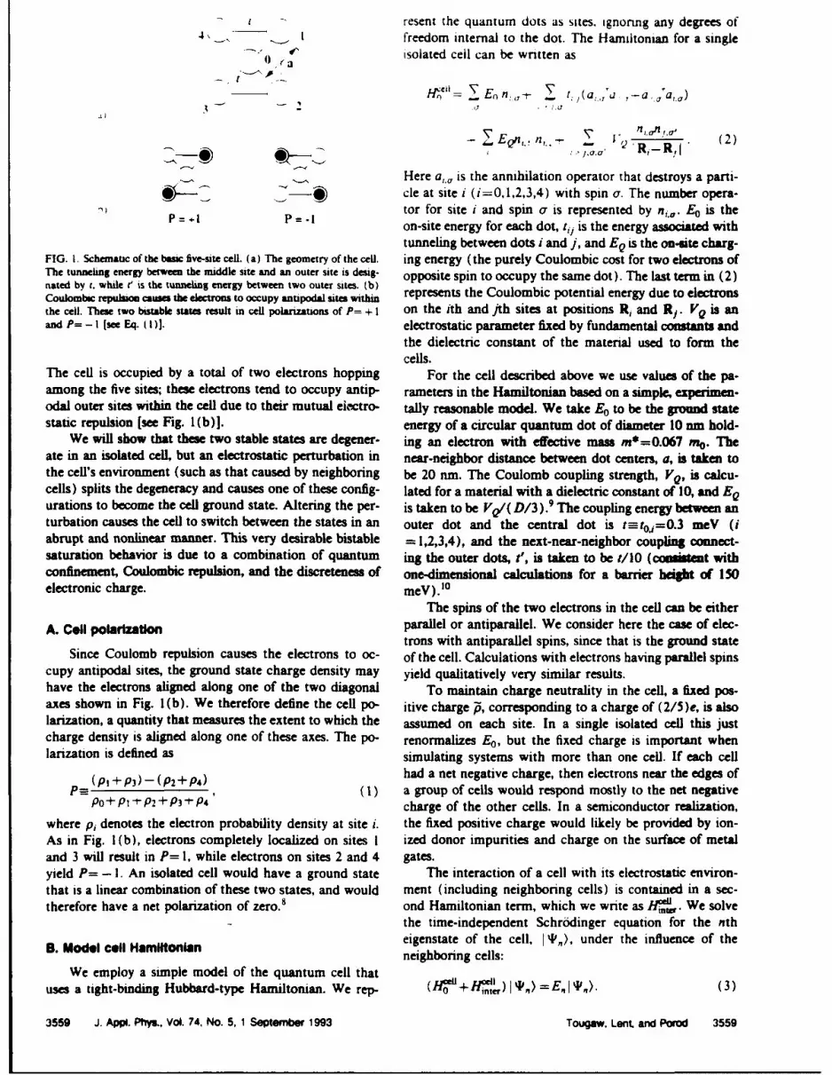
-t resent the quantum dots as sites. ignorng any degrees of-, _.- .__. ! freedom internal to the dot. The Hamiltontan for a single
isolated cell can be written as
3 -
E~n,. ,n, 'VQ " _ (2).-'- R,_R,J
Here a, is the annihilation operator that destroys a parti--- cle at site i (i=0,1,2,3,4) with spin a. The number opera-
-=* P=-tor for site i and spin a is represented by ni.,. E0 is theon-site energy for each dot, t:i is the energy associated withtunneling between dots i and j, and EQ is the on-site charg-
FIG. I. Schematic of the basic five-site cell. (a) The geometry of the cell. ing energy (the purely Coulombic cost for two electrons ofThe tunneling energy between the middle site and an outer site is desig- opposite spin to occupy the same dot). The last term in (2)nated by c, while r' is the tunneling energy between two outer sites. (b)Coulombic repulsion cause tie electrons to occupy antipodal sites within represents the Coulombic potential energy due to electronsthe cell. These two bistable states result in cell polanzataons of P= + I on the ith and jth sites at positions Ri and Rt. VQ is anand P= - I [see Eq. (M)]. electrostatic parameter fixed by fundamental constants and
the dielectric constant of the material used to form thecells.
The cell is occupied by a total of two electrons hopping For the cell described above we use values of the pa-among the five sites; these electrons tend to occupy antip- rameters in the Hamiltonian based on a simple, experimen-odal outer sites within the cell due to their mutual eiectro- tally reasonable model. We take E0 to be the ground statestatic repulsion [see Fig. 1 (b)]. energy of a circular quantum dot of diameter 10 am hold-
We will show that these two stable states are degener- ing an electron with effective mass m*=0.067 mo. Theate in an isolated cell, but an electrostatic perturbation in near-neighbor distance between dot centers, a, is taken tothe cell's environment (such as that caused by neighboring be 20 nm. The Coulomb coupling strength, VQ, is calcu-cells) splits the degeneracy and causes one of these config- lated for a material with a dielectric constant of 10, and EQurations to become the cell ground state. Altering the per- is taken to be VQI( D/3).9 The coupling energy between anturbation causes the cell to switch between the states in an outer dot and the central dot is t-roj=0.3 meV (iabrupt and nonlinear manner. This very desirable bistable = 1,2,3,4), and the next-near-neighbor coupling connect-saturation behavior is due to a combination of quantum ing the outer dots, t', is taken to be t/l0 (cosistent withconfinement, Coulombic repulsion, and the discreteness of one-dimensional calculations for a barrier height of 150electronic charge. meV).10
The spins of the two electrons in the cell can be either
A. Cell polarization parallel or antiparallel. We consider here the case of elec-trons with antiparallel spins, since that is the ground state
Since Coulomb repulsion causes the electrons to oc- of the cell. Calculations with electrons having parallel spinscupy antipodal sites, the ground state charge density may yield qualitatively very similar results.have the electrons aligned along one of the two diagonal To maintain charge neutrality in the cell, a fixed pos-axes shown in Fig. 1 (b). We therefore define the cell po- itive charge 0, corresponding to a charge of (2/5)e, is alsolarization, a quantity that measures the extent to which the assumed on each site. In a single isolated cell this justcharge density is aligned along one of these axes. The po- renormalizes E0 , but the fixed charge is important whenlarization is defined as simulating systems with more than one cell. If each cell
!(PI+P3)-(P2+P4) had a net negative charge, then electrons near the edges ofP- ,P P (1) a group of cells would respond mostly to the net negativePO-+PI-t--P2+P3 -t-P4 charge of the other cells. In a semiconductor realization,
where pi denotes the electron probability density at site i. the fixed positive charge would likely be provided by ion-As in Fig. 1(b), electrons completely localized on sites I ized donor impurities and charge on the surface of metaland 3 will result in P= 1, while electrons on sites 2 and 4 gates.yield P= - 1. An isolated cell would have a ground state The interaction of a cell with its electrostatic environ-that is a linear combination of these two states, and would ment (including neighboring cells) is contained in a sec-therefore have a net polarization of zero. 8 ond Hamiltonian term, which we write as /,.w We solve
the time-independent Schrodinger equation for the nthB. Model cell Hamiltonlan eigenstate of the cell, I qP,,), under the influence of the
neighboring cells:We employ a simple model of the quantum cell that
uses a tight-binding Hubbard-type Hamiltonian. We rep- (HBO0 +H %,,)I, = E, I'Y. (3)
3559 J. Awi. Phys., Vol. 74. No. 5, 1 September 1993 Tougaw, Lent, and Porei 3559

1 .0 ,
0 5~ > 0.2-
~-0.0 -00
-0.5 "' -0.2 - -
-0.4 "_
-1.0 -0.5 0.0 0.5 1.0 -1.0 -0.5 0.0 0.5 1.0P, P.
FIG. 2. Cel-ovll rpme 1 fncuoua for the bmic five-ate cells shown m FIG. 3. The lowest four agenstate energia of cel I induced by thethe nme. Thssi t•o Pola, , • P, induced tn cell I by the Axied polmnizaton of cell 2. Thse muci show that the lowest two meo statespolazationm of ids mamgbor. P2. The soid line correponds to anuparalrl always coraupood to the smie polartzation dretiom. a in time dive.spins. and the domed he to peraild spum The two me nearly degename. Slight evchag•e slitlng e5 between spatialy gmIk b•a d qasmiodyapecnlly for tiantly large valum of P2. anwyutnetic stat breaks t&e fourfold degcnmcy for very -nal vains
of P2.
The total Hamihoni is diagonalized directly in the basisof two-partice ate kets. We calculate the single-particledensity, pi, from the two-particle ground-state wave func- in the range - I,+ +1]. The ground state polarization of
tion I1T) by finding the expectation value of the number cell 1, P,, is then computed for each value of P2 , as de-
operator for site i: scribed in the previous section. Thus, we can plot the in-duced polarization of cell I as a functim of the pokliji-
A= (Ioinfolo). (4) don of cell 2. This function P,(P 2 ), whIw cal theor cell-cell responne function, is one mn n.o bho weall a
We can thin am tdaoe densities to calculate the cell polar- cell will operate in a quantum cellular amr ac-istio
ization P as in Eq. (1). tu,Figure 2 shows the cell-cell response function for the
C. eMCUng tha O W r pong hxwj ou standard cell. The highly nonlinear nature of the responseindicates that a small polarization in cell 2 causes a veryTo be usdul in cellular automata-type ahiectures, strong polarization in its neighbor, cell 1. The figure also
the state of a cell must be strongly influenced by the states strong polarization of cell I s in very quickly
of neighboring cell To demostrate how one of thee tw to a value of + I or -1 . This bistable saturation is the basisis influenced by te state of its neighbor, consider the two ofth quanitum celua autmata, iminm tmmm we
cells shown in the inset to Fig. 2. The cell centers are oa en tim cell i zation we
separated by a distance of 3a-=60 nm. We assume cell 2 assign the bit value of into the P= +1 state and the bit
ha a given polarization P2 and that the electron density on value0 tothe P=- lstate. Since the cell Istalmost always
the central site is negligible. This means that the charge in a highly polarized state (-I P1 1), the state of the cell
density is completely determined by the cell polarization, will be indeterminate only if the electrostatic environmentFor the corresponding electron density on each site of cell due to other cells is perfectly symmetric.2, we calculate the electrostatic potential at each site of cell Figure 3 shows the lowest four eigenmergies of cell I1. This additional potential energy is then included in the as a function of the polarization of cell 2. This sbows thatHamiltonian for cell 1. Thus the perturbing Hamiltonian the perturbation due to the polarization of cell 2 quicklycomponent is separates the states of opposite polarization. For a com-
pletely polarized standard cell, the excitation energy froml:J =l= h V! n ,4, (5) the ground state to the first excited state with opposite
where t ' polarization is about 0.8 meV. This corresponds to a tem-perature of about 9 K.
=( p-) The abruptness of the cell-cell response function de-P= X VQ - R (6) pends on the ratio of the tunneling energy, t in Eq. (2), to
S1Rj- R,, the Coulomb energy for electrons on neighboring sites. Theis the potential at site i in cell m due to the charges in all magnitude of the tunneling energy depends exponentiallyother cells. We denote the position of site j in cell k as on both the distance between dots and the height of theRk,,, and the electron density at site j in cell k as pk. The potential barrier between them. Figure 4 shows the cell-total Hamiltoman for cell I is then cell response function for different values of the tunneling
R-0=/R +/'. (7) energy t. The switching becomes more abrupt as t de-creases. Of course, if t goes to zero, the tunneling would be
The two-electron time-independent Schrddinger equation completely suppressed and no switching would occur. Ex-is solved using this Hamiltonian for a seres of values of P2 tremely small values of t would similarly slow the switch-
3560 J. AM*. Pys. Vol. 74, No. 5, 1 Ssprsr 190 Tougw., Lefnt. end Por 3560

H) peratures up to 4.2 K. the response is good. but for highertemperatures it would probably be unacceptable for use in
0.5 - a QCA.
Note that this maximum operating temperature will.- 0.0 - increase as the size of the cell decreases. Thus, although a
20 nm design rule requires cryogenic temperatures forsatisfactory operation, the de.ign scales to smaller sizes
-1.0 __..... "_easily and a much smaller, possibly macromolecular,
-0.10 -0.05 0.00 0.05 0.10 implementation" would work at room temperature.P,
III. ALTERNATIVE QUANTUM CELLS
FIG. 4. The cell-cell response function of the basic five-site cell for var- While the cell described above has demonstrated antous values of the parameter t in Eq. (2) (after Ref. 4). The induced excellent cell-cell response, there is no reason to discountpolarization in cell I is plotted as a function of the polarization of its other possible cell designs. Slight modifications to this cellneighbor, cell 2. The curves corrpesond to t=0.2 meV (solid line), t=0.3 give rise to a family of similar cells whose behavior canmeV (dotted line), t=0.5 meV (dashed line), and t=0.7 meV (dot-dashed line). Note the horzontal axis only shows P2 in the range [-0.1, provide insight into the nature of the system.
-o.11j. In looking for other model cells, there are several ap-proaches we can take. The most obvious of these is to alterthe number of sites and their geometric arrangement. Al-ternatively, the cell occupation can be altered. Finally, tun-
ing time. For t=0.3 meV, the standard cell value, we es- neling between the intracellular sites can be increased, de-timate the tunneling time as i/t = 2 p. creased, or effectively eliminated by varying the potential
D. Nonzero temperature cell-cell response barriers between the sites.
We extend the calculation of the cell-cell response A. Four quantum celtfunction to nonzero temperatures by calculating the ther- In this section we will investigate the cell-cell responsemal expectation value of the electron density at each site of of four different quantum cells. While these four are rep-the cell, resentative of the sort of cells one might consider, they in
X•,I , q$.Ji.T.e qj 1 k.BT) no way exhaust the study of new cell designs.
Pi= ((0,)) = 1 e-EI(kBT) (8) The first cell, included mainly as a standard by whichto judge the others, is the original cell described above witht=0.3 meV. This will be called cell A. Next will be the
Evaluating the thermal average requires knowledge of the same cell with no tunneling between the outer neighborsexcited states of the cell as well as the ground states. Using (t'= 0). We will refer to this as cell B. Cell C omits thethe results of Eq. (8), the polarization of the cell can be presence of the central site and allows tunneling only be-calculated as before using Eq. (1). The results of such a tween the four outer sites. Finally, cell D inhibits tunnelingcalcuiation for the standard cell (with the next-near- even further, allowing it only between sites 1 and 2 andneighbor coupling t' =0) are shown in Fig. 5. The curve between sites 3 and 4. Schematic diagrams of these fourfor T=O is the same as in Fig. 2. The nonlinearity of the cell designs are shown in Fig. 6(a).response degrades as the temperature incre.•ses. For tem- In a semiconductor realization of these cells, the min-
imum spacing between nearest-neighbor sites will be lim-ited by the fabrication technology. For this reason, thesecells are designed with a constant 20 nm design rule (the
1.0- nearest neighbors in each cell are 20 nm apart). While thismakes cells C and D smaller, it is the most physically
o.5- reasonable way to compare their operation. The spacingbetween interacting cells is set at three times the near-
S 0.0 - T=2 K 4 neighbor dot spacing.
r.,\ K\\ It is possible to consider cell B as an approximation to-0.5 -. ..- Tl$K cell A that neglects tunneling between outer neighbors. In
- -- Tri K reality there will always be a certain amount of tunneling
-1.0 .0.5 0.0 0.5 1.0 between outer sites, but this tunneling can be made arbi-
p. trarily small by selectively increasing the potential barriersbetween the outer sites. The same increase in potential
FIG 5 The cell-cell response functionJ'or the standard cell with t'=O at barriers would be needed to suppress horizontal tunneling'anous temperatures. The response degrades as temperature increases, in cell D.Above 4.2 K. the response would be unacceptable for use in a QCA. This Figure 6(b) shows the cell-cell response functions formaximum operating temperature is highly dependent on the physical sizeof the cell; molecule-sized cells would behave in a satisfactory manner up these four cells. This figure shows that cells A and B haveto room temperature. very similar responses, and both are superior to cells C and
3561 J. Apo. Phty.. Vol. 74, No. 5, 1 September 1993 Tougaw, Lent. and Porod 3561

lt 11.0.
3 2 p2 0 0, 0.5r
S0.0k
1.0~ -0.51-
0. ~ f/"-0.5 0.0 0.5
0.0 P-
-0.5 ~FIG. 8. Cell-cell luoefunction for the barn5sic A ediecl ooempnd by
-1.0 C A) 13 three eknu~t orb a celluaalso unscoeptbleahistIsm of aQCA.
-1.0 -0.5 0.0 0.5 1.0p I togyplaieee for fully polarized nsighibmu. This
indicates that such cells would perform very poorly a the
FIG. 6. Four geomietic variations on the aimple model quantum cell. (a) basis of a quantum cellular automate..
Schematic diagratns of the four aeUl. Cull Cmin D occupy leas am. butall four cells are dhrawn with the -am minimum speacng between neighs. C. Quanftum das8110 and doUble Waftbom~ Cells B and D will require potential vanabo betwe the sitern toselectively inhibit tunneling. (b) The cell--cel U~s function for each Proposals have been made for oua~dcwsm "quantsosof theme cell demwm. Cel B has th bes but the imot dash" cells that aperqualitatively ai le douas weover Aisan-lH- have disamond here." In this sectum. wwk=I the
cell-cell rupoMe function Of uingwa qdashes and omaethis to a very "&K&W* WMN
D. Thus, elimination of the central site as in cells C and D well to show how impoutant the dim.he - sb idegrades the response. This leads us back to the five-sate charp is to the nonlinearity of the uea as omcdca suencell we originally considered. Since the complete suppres- in the previou sections.sion of next-nea-neighbor coupling as in cell B might in- Since these cells are of a more sptamilb continuosentroduce additional fabrication difficulty with little improve- nature than cells previously considered tin site repres.ment in the cell response, cell A may be the most practical tanon is no longer usefuil. Each cell wil be smod asi aof these four cell designs. n-ieuoa hard-walled square wall of width 30 sm.
The two call awe separated by a dih..N29 m Cdiensions are similar to those of the cub&wsdboe
0. One- and tJ..... eond. cello We use the finite element method to solve thq single-
As an alternative to chnaning the geometry of the cell, electron time-independent Schridinge eqationc for eachwe cn aso lte th elctrn ocupncy Fiure7 sows one-electron cell. The geometry used to calculste the cell-we cn aso lte th elctrn ocupncy Fiure7 sows cell response function is shown schematically in Fig. 9(a).
the cell-cell response function for cell A occupied by a Since these cells have only a single axids along which tosingle electron. and Fig. 8 shows the response for the sam distribute the electronic charge, a new ddliton of polar-cell with three electrons (two parallel spins, one antipar- ization must be introduced. The new defiition, whichalle). These nearly linear response flilctions, never becomei takes into account the continuous nature of the probability
density, is
P=f -L2 P(X)dX-f pL~ d (9)1.0 fLP(X )d~x
0.5 Because of its continuous nature, the charge density in the"Idriver" cell is no longer uniquely determined by specify-
~-0.0 ing the cell polarization. We therefore fix the charge den-sity to be constant in each half of the driver cell.
-0.5The cell-cell response function calculate for such asystem is shown in Fig. 9(b). As this figure shows, the
-1.0 tresponse is quite linear, and cell 1 is virtually unpolarized,-1.0 -0.5 0.0 0.5 1.0 even for afMy polarized neighbor. The electron probabil-
- 2 ity density as afunction of position for cell 1 with afullyFIG 7 Th cll-el repose untio fr te mas fve-uecel ~polarized neighbor (P2 =1I) is shown in Fig. 9 (c). The
by a single electron. The weak response uisdcates that such a cel is probability density is nearly symmetric about the center ofumiutablit a the bai of a QCA. the cell as we would expect for such a small polarization.
3W6 J. Appi. Ptq.. Vol. 74. No. 5. 1 Sepamnber 196M Tougaw, Lent, wid Poen 38W

4 i el 'I ( ll2 edll 1 0ell2
20..M 20 R.
4)O
i 0-
1'bi 0 .) )0 5 :0b) 0 s 05 0 o5 P
* 0
1) 5 0 ISý(M
FIG. 9 nw -qwMim d" a QCA CCUl. (a) A Kbincbmac doqirss of FIG. 10. The double wnd w a QCA cell. (a) A uhoofi df of 'hethe ceflllr arra~miet Th e mgill Md Ipacu a asiar to ibmi 0( the cellula mFOROMg The 1011inaMIN wm e dism to diibm Of ftS S.bmc Ave-sit cel w Fig. I (a). Each =elis modeliad w a One-dimsowil The* sadde thb of mhk c ooioni alS 13 mV bmvw 00 self w Uspuna*,ne squsuw weill. nth cd-llý rpo a show in (b. NMdwi h the ad basso, of the amil. (b) T11e cad&c - pe fhn fo subh =
verW m olyshows Pov ed ramp (-0-i. +0.l11. (c) The one- arrispouss. Now de thu 'he WKSmu a OW mow 8 P1 CO dW ndimameW chep I, a mil 2 fm a fully pokrasd sughbo 1.0.O+i.L% (c) The m.hesowlmdcamp AmqMasy 2 ra MY(p, - 1). Te mandy sy chai ,dp d-md-) yiel a vay low poho- pohIbm*Ww CP, - 1). Th lbs * uyinam un d~ d yoazaina. maWm M a ad them a alliow Wlm poklenmd.
A related cell. the double well, is shown schemaitically barriers surrounding it.'4 T'herefore, almost the entirein Fig. 10(a). It is a quantum well of the same dimensions wavefuniction will become localized in one-beg of the cell ifas in Fig. 9(a), but the potential in the middle third of the a small asymmetry in the electrostati envirommeas is in-well has been rained by 150 meV. This cell is also very troduced. This fact is demonstrated in Fig. 10(c), whichsimila to half of cell D from the last section. so we would shows nearly all the charge density on the rigt beg of theexpect its response to be much better than that of the sam- cell. Suice there as no barrier in the middle of the qullampie quantum dash. dash to isolate the top and bottom of the cell, no sach
The calculated response. shown in Fig. 10(b). is in- localization behavior is seen there, and the charge desaitydeed much better than that of Fig. 9(b). Its nonlineanty is always nearly symmetric about the center of the well.and saturation properties are very similar to those of cellsC and D in Fig. 6(b). This response shows that one- IV. MULTUPLE NEXMOR INTERACTlONelectron cells can be used to provide the required nonlinearresponse, but it is also possible to view each pair of these Thus far, we have only considered the interaction be-cells as a single two-electron cell, which becomes geomet- tween a cell and a single neighboring cell. The naturalnicaly very similar to cell D of Fig. 6 (a).- extension of this is to investigate the effect of multiple
The fact that such a seemingly small change in the neighbors on the state of a cell. Since this implese consid-nature of the cell should cause such a profound change in ering a system that contains several cells and thereforethe cell-cell response function-is linked to the fact that several electrons, we cannot use the direct solution methodelectron charge is discrete in regions surrounded by high described earlier for treating a single cell. For the analysispotential barriers. That is to say, the expectation value of of such systems, we treat the physics within ich CellUthe number operator approaches an integer value as the before, including exchange and correlation Mc exactly,region becomes more and more isolated by the potential The intercellular interaction is treated 1e3-0mmalyu-
3563 J. ApoI. Phys.. Vol. 74. No. 5. 1 Sepwtemb 1 N3 Tougew, Lenl anid Pale 35M
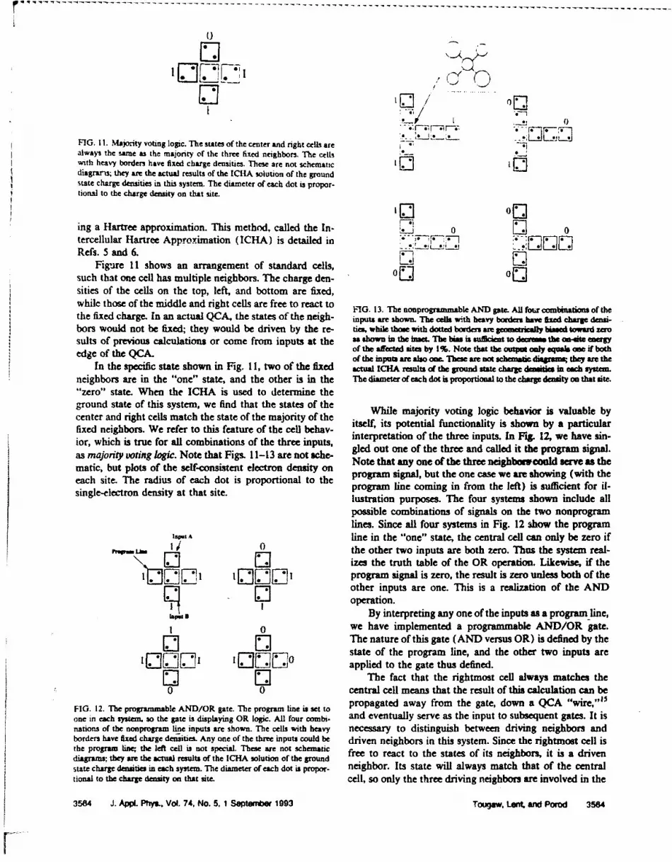
0
r ._.1
FIG. 11I. Majority voting logic. The states of the center and right cells are I- .-'always the same as the majority of the three fixed neighbors. The cells A_- ,o.jwith heavy borders have fixed charge densities. T'hese are not schematic F. J' I
disgriuns, they ame the actual results of the ICIRA solution of the groundstate charge densities in this system. The diameter of each dot is propor-tional to the charge density on that site.
ing a Hartree approximation. This method, called the In- 0 0tercellular Hantree Approximation (ICHA) is detailed in " "-
Fig-mre I1I shows an arrangement of standard cells, E Csuch that one cell has multiple neighbors. The charge den-°l°dsities of the cells on the top, left, and bottom are fixed,while those of the middle and right cells are free to react to
FIG. 13. The nooprormale AND gate- All four combitations of thethe fixed charge. In an actual Q4CA, the states of the neigh- inputs are shown. The cel wrth heavy bodr haftfied chaW d •i-bors would not be fixed; they would be driven by the re- ties, wh& those with dotted borders am gemtral bigdtoward wosuits of previous calculations or come from inputs at the as ,lawn in the imaci. The bwIas it ,fideat to deomiari the on-ame energy
edge f theQCA.of the aff'ected sites by I%. Note that the output only equalis we if btxhedg o th QA.of the inputs am also one- Ths tan not tdscbmadiagnims they an the
In the specific state shown in Fig. 1 1, two of the fixed acu ICHA resuts of the Inro sadte chaire dwaitie, m eth systemanneighbors are in the "one" state, and the other is in the The diamete of each dot is proportionail to the ehwpg density on that site.".zero" state. When the ICHA is used to determine theground state of this system, we find that the states of the While majority voting logic behavior is valuable bycenter and right cells match the state of the majority of the itself, its potential functionality is shown by a particularfixed neighbors. W e refer to this feature of the cell behav- i t r rt to ft et r ei p t .I i .1 ,w a esnior, which is true for all combinations of the three inputs, itrrtto ftetreipt.I i.1,w aesn
as mjorty otig lgic Noe tht Fgs.11-3 ae nt she- gled out one of the three and called it the program signal.matc, ut los o th sef-onsstet eecrondenityon Note that any one of the three neighboetweod serveas the
eatch bute plthrdis of th elfchonsistn elroprina destyonth program signal, but the one case we are showing (with theeachgsite.eThe radiusiof eachhdt isite.rina o h program line coming in from the left) is sufficient for il-
singe-eecton ensiy a tht ste.lustration purposes. The four systems shown include allpossible combinations of signals on the two nonprogramlines. Since all four systems in Fig. 12 show the program
Input A line in the "one" state, the central cel can only be zero ifS0 the other two inputs are both zero. Thus the system real-•'-- •• .i•'l.• ••'''izes the truth table of the OR operation. Likewise, if the
t .7 F. I' F-41 program signal is zero, the result is zero unless both of thei• ['-71other inputs are one. This is a realization of the AND
I. I operation.,opet B By interpreting any one of the inputs as a programnfine,
10 we have implemented a programmable AND/OR gate.[• • The nature of this gate (AND versus OR) is defined by the
In "1 " "I- ._ ".. -•-I'Oh.]_ .J state of the program line, and the other two inputs are
1'., 0applied to the gate thus defined.•'• •The fact that the rightmost cell always matches the
0 0 central cell means that the result of this calculation can beFIG. 12. The programmable AND/OR gate. The program Mie 'IS set to pragtd wyfomheaeonaQA ie,'one in each sysem, so the gate is displaying OR logic. AUl four combi- and eventually serve as the input to subsequent gates. It isnations of the nonprogram ýne inputs are shown. The cells with heavy necessary to distinguish between driving neighbors andborders have fixed charge densities. Any one of the three inputs could be driven neighbors in this system. Since the rightmost cell isthe program line; the let cell is not special. These are not schematic fe oratt h ttso t egbri sadiedisgr-am;: they ame the actual results of the ICHA solution of the groundstate charge demitkes in each system. The diameter of each dot is propor- neighbor. Its state will always match that of the centraltional to the chap denterity on that site cell, so only the three driving neighbors are involved in the
3564 J. Apl Phys, Vol. 74, No. 5, 1 Setme 1993 Tougaw, Len and Porod 3564

majonty voting. Of course. once the signal is propagated that future realizations of these cells will be on a macro-away from this gate, the outgoing cells are being driven molecular basis. Another challenge, sensing the presenceand can be used as driving neighbors for subsequent gates. or absence of a single electron without disturbing the sys-
A dedicated, nonprogrammable implementation of the tern, necessary for reading the output state of a QCA de-AND gate is shown in Fig. 13. This system has only two vice, has been successfully addressed.17driving inputs: there is no program signal. The role previ- In conclusion, we have explored the interaction ofously played by the program signal, biasing the central cell neighboring quantum-dot cells. We have defined the cell-,,o it can only be in the one state if both of its neighbors are, cell response function, which characterizes the nonlinearityis performed by slightly enlarging the two quantum dots on of the coupling between cells, and thus determines suitabil-sites I and 3 in the central cell."e This means that the ity of a particular cell design for quantum cellular autorm-
ground state of the isolated cell is no longer an unpolarized ata implementations. Several cell designs that exhibit thestate; the cell is biased toward the zero state and can only required nonlinear response and bistable saturation havebe persuaded to enter the one state if both of its driving been examined. Temperature effects degrade cell perfor-neighbors are one. Again, the signal propagates away to mance, but analysis in this simple model suggests that op-the right and can be used to drive subsequent gates. A eration at 4.2 K should be within the reach of semiconduc-dedicated OR gate can similarly be implemented by enlarg- tor implementations. When a cell has several neighbors, itsing sites 2 and 4, biasing the cell toward the one state. It state is determined by the state of the majority of the neigh-will only be in the zero state i" both of its driving neighbors boring cells. This majority voting logic makes possible theare also zeros. construction of programmable AND/OR logic gates as
well as dedicated AND and OR gates.V. DISCUSSION
With the above results, we have demonstrated several ACKNOWLEDGMENTSquantum-dot cells suitable for implementing a quantum We gratefully acknowledge stimulating conversationscellular automata architecture. Examination of the cell- with Gary H. Bernstein of the Notre Dame Nanoelectroniccell response function shows that for appropriate cell de- Group. This work was supported in part by the Air Forcesigns, the state of a cell is influenced very strongly by the Office of Scientific Research and the Office of Naval Re-state of its neighbors. The highly nonlinear response of the search. This material is based in part upon work supportedcell suggests that a signal that has become degraded by under a National Science Foundation Graduate Fellow-noise will be restored to full polarization by subsequent ship.cells in the array.15 In this way, the bistable saturation ofthe quantum cell is analogous to the gain in a conventional 'T. Toffoli and N. Margolus, Cellular Automata Machine A New En.digital device. vironmentfor Modeling (MIT Press, Cambridge, MA, 1987).
We have assumed throughout that the many electron 2L. D. Chus and L. Yang. IEEE Trans. Circuits Syst. 35, 1257, 1273(1988).
system 3 R. T. Bate, Bl1. Am. Phys. Soc. 22, 407 (1977); J. N. Randall. M. A.in the ground state and then be driven into an excited state Reed, and G. A. Frazier, 5. Vac. Sci. Technol. 97. 1398 (1989); D. K.by externally changing the states of input cells near the Ferry, L A. Akers, and E. W. Greeneich, Ultra Large Scalintercon-edge of a QCA array. Inelastic processes, which are usually nected Micraelectronics (Prentice-Hall, Englewood Cliffs, NJ, 1988); J.
ery detrimental to the operation of quantum devices, then N. Randall, A. C. Sesbaugh, Y.-C. Kao, 1. H. Luscombe, and B. L.Newell, J. Vac. Sci. Technol. B 9, 2893 (1991).drive the system back to a new ground state corresponding 4C. S. Lent. P. D. Tougaw, and W. Porod, Appl. Phys. Lett. 62, 714
to the new inputs. The details of the temporal evolution of (1993).
the many-electron system as it relaxes to its ground state IC. S. Lent, P. D. Tougaw, W. Porod, and G. H. Bernstein. Nanotech-nol4 49 (1993).
are very complicated. In the QCA scheme, we rely on the 6C. S. Lent and P. D. Tougaw, (unpublished).properties of the system ground state and not the details of tothers have attempted to apply our QCA architecture ideas (Refs. 4-6)the relaxation prcess for doing the computation. This idea to a system where the information is encoded in the spin of the electron.of "computing with the ground state" and the related con- See S. Bandyopadhyay; B. Dasr;and A. Miller (unpublished).of sysomp h th emdstare di sed mreld ton- The polarization so defined is not to be confused with a dipole moment.cept of "edge-driven" systems are discussed more thor- For the situations we consider here, the ground state of the cell has nooughly in Ref. 5. dipole moment, though it may have a quadrupole moment. The cell
The behavior of lines of these cells, the most basic (and polarization simply measures the degree to which the electronic chargemportant) components of a quantum cellular automaton, is aligned and the direction of that alignment."For the standard cell, we take E0 to be the Coulomb energy of twois discussed in Ref. 6. The results show an excellent exam- electrons separated by one-third the dot diameter D, a physically res-
pile of the restoration of full signal strength after degrada- sonable first approximation.tion by noise. In addition, it shows that the particular set of '0Referenc- 6 examines the behavior of lines of cells as all these Hamil-parameters we chose in Sec. II B is not critical; there is a tonian parameters are vaned. The bistable behavior we examine here is
not critically dependent on a particular choice of these parameters, butwide range of parameter values for which the cells transmit holds for a wide range of parameter choices.information from one cell to another. 'For a review of the current state, see G. J. Ashwell, Ed., Molecular
Clearly, fabrication of these devices presents a major Electronics (Wiley. New York, 1992).challenge in the realization of QCA devices, but s 2Control of cell occupancy is clearly important in implementation. The
ability to control quantum dot occupancies over as many as 10 dotsductor realizations of such systems using new nanolitho- using a backgating technique has recently been reported by B. Meurer.
graphic techniques should be possible. It is also possible D. Heitmann, and K. Ploog, Phys. Rev. Lett. 68, 1371 (1992).
3565 J. Appl. Phys., Vol. 74, No. 5. 1 September 1993 Tougaw, Lent, and Pored 3565
"P. Bakshi. D. A. Broido. and K. Kempa. J. Appl. Phys. 70. 5150 'Enlarging the quantum dots lowers the on-site energy 4and makes It(1991). energetcay more faiorable to occupy the largtw dots.
14See tie discussion MWd tWo~eiecrron Calculation by C. S. Lent nPao. -s cargIn£aicdser14Setb, dclz~aadtw~eectonc~cuaocbyC S.Let, in Nano. "Noninvasive probing of single~electron charging in a semicondueWo
sgruohvses and Mwcwapic Sysnte, edited by W. P. Kirk and M. A.Reed (Acadenic, Boston. 1992). p. 183. qunm dot has recently been reported by M. Field, C. 0. Smith. K.
"See the discussion of the behavior of lines of cells as a binary wire n Pepper, J. E. F. Frost, G. A. C. Jones, and D. 0. H n.A Phys. Rev.
Ref. 6. Lett. 70, 1311 (1993).
356 J. Appl. Physt., Vol. 74, No. 5. 1 SePtsbr 1993 Tougaw. Lent, nd Poxod 3566
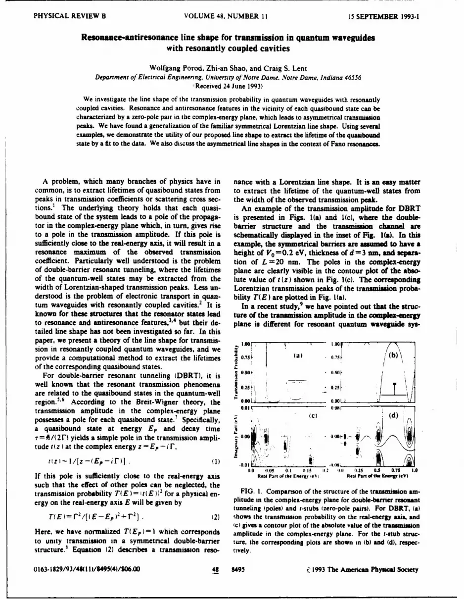
PHYSICAL REVIEW B VOLUME 48, NUMBER 11 15 SEPTEMBER 1993-1
Resonance-antiresonance line shape for transmission in quantum waveguideswith resonantly coupled cavities
Wolfgang Porod, Zhi-an Shao, and Craig S. LentDepartment of Electical Engineering, University of Notre Dame. Notre Dame. Indiana 46556
, Received 24 June 1993)
We investigate the line shape of the transmission probability in quantum waveguides with resonantlycoupled cavities. Resonance and antiresonance features in the vicinity of each quasibound state can becharacterized by a zero-pole pair in the complex-energy plane, which leads to asymmetrical transmissionpeaks. We have found a generalization of the familiar symmetrical Lorentzian line shape. Using severalexamples, we demonstrate the utility of our proposed line shape to extract the lifetime of the quasiboundstate by a fit to the data. We also discuss the asymmetrical line shapes in the context of Fano resonances.
A problem, which many branches of physics have in nance with a Lorentzian line shape. It is an easy mattercommon, is to extract lifetimes of quasibound states from to extract the lifetime of the quantum-well states frompeaks in transmission coefficients or scattering cross sec- the width of the observed transmission peak.tions.' The underlying theory holds that each quasi- An example of the transmission amplitude for DBRTbound state of the system leads to a pole of the propaga- is presented in Figs. l(a) and l(c), where the double-tor in the complex-energy plane which, in turn, gives rise barrier structure and the transmission channel areto a pole in the transmission amplitude. If this pole is schematically displayed in the inset of Fig. 1(a). In thissufficiently close to the real-energy axis, it will result in a example, the symmetrical barriers are assumed to have aresonance maximum of the observed transmission height of Vo =0.2 eV, thickness of d =3 n, and separa-coefficient. Particularly well understood is the problem tion of L = 20 nm. The poles in the complex-energyof double-barrier resonant tunneling, where the lifetimes plane are clearly visible in the contour plot of the abso-of the quantum-well states may be extracted from the lute value of t (z) shown in Fig. 1(c). The correspondingwidth of Lorentzian-shaped transmission peaks. Less un- Lorentzian transmission peaks of the transmission proba-derstood is the problem of electronic transport in quan- bility T(E) are plotted in Fig. 1(a).tum waveguides with resonantly coupled cavities.2 It is In a recent study,9 we have pointed out that the struc-known for these structures that the resonator states lead ture of the transmission amplitude in the camplex-energyto resonance and antiresonance features, 3' 4 but their de- plane is different for resonant quantum waveguide sys-tailed line shape has not been investigated so far. In thispaper, we present a theory of the line shape for transmis- 1.00!sion in resonantly coupled quantum waveguides, and we aprovide a computational method to extract the lifetimes 0.75 (a) os/75of the corresponding quasibound states. -,
For double-barrier resonant tunneling (DBRT), it is 0.50 1...
well known that the resonant transmission phenomena 0.2s. I' 0.23are related to the quasibound states in the quantum-wellregion.' 6 According to the Breit-Wigner theory, the 0.e- 0.00 .transmission amplitude in the complex-energy plane - 0.08,(d- ~(C)• (d)possesses a pole for each quasibound state.' Specifically, ,a quasibound state at energy Ep and decay time ,,,'= A/(2r) yields a simple pole in the transmission ampfi- -0.0 0~e ' l ., . . 00®-t • .
tude t(z) at the complex energy z =Ep -irF,
z)~l/[z-(Ep-iF)]) -0.01 L 1 \ 0.0' 0
0.0 0.05 0.1 0.15 12 WI 0.25 0. - 0.7S 1.0If this pole is sufficiently close to the real-energy axis Real Part oathe EnenLv y,'I Rent Paor olthF. .wr (eV)
such that the effect of other poles can be neglected, thetransmission probability T(E ) = I (E ); 2 for a physical en- FIG. I. Comparison of the structure of the transmission am-ergy on the real-energy axis E will be given by plitude in the complex-energy plane for double-barrier resonant
tunneling (poles) and t-stubs (zero-pole pairs). For DBRT, (a)T(E )= /[(E-Ep )2r]. (2) shows the transmission probability on the real-energy axis, and
(c) gives a contour plot of the absolute value of the transmissionHere. we have normalized T(Ep)- -I which corresponds amplitude in the complex-energy plane. For the t-stub struc-to unity transmission in a symmetncal double-barrier ture, the corresponding plots are shown in (b) and (d), respec-structure. Equation (2) describes a transmission reso- tively.
0163-1829/93/44g1l!)/U495(4)/S06.00 48 8495 6 1993 The American Physical Society

8496 WOLFGANG POROD, ZHI-AN SHAO. AND CRAIG S. LENT 48
as compared to the above case of double-barrier resonant q = 1 Ep - E,) / r . Comparing our approach to Fano's,'
tunneling. In essence. each resonator state in a we note that e has a similar meaning where Ep, the realquantum-wire structure gives rise to a zero-pole pair in part of the pole energy, corresponds to E e,, the energy ofthe complex-energy plane. where the zero always occurs the resonant state. For the parameter q, our approachon the real-energy axis. As a consequence, there exist yields a simple expression which could not have been in-transmission zeros, and the zero-pole pairs lead to asym- ferred from Ref. 11. Apparently, Fano's line shape corre-metric resonance and antiresonance features in the sponds to a zero-pole structure in the complex-energytransmission probability with non-Lorentzian line shapes. plane. a fact which has not been noted before.As an example, we show the behavior for a t-stub struc- Given a certain transmission curve, we now can fitture,10 as schematically shown in the inset of Fig. l(b), each resonance and antiresonance feature to obtain thewhich consists of a main transmission channel and a dan- lifetime of the corresponding quasibound state. Usinggling wire of length L = 10 nm. For this so-called strong- the known energies of the transmission zero, E 0, andly coupled t-stub, 9 the transmission probability is shown transmission one, EI, we can determine the energy of thein Fig. 1 (b) and a contour plot of the absolute value of t in pole asthe complex-energy plane is displayed in Fig. I(d). Zero-pole pairs are clearly visible which correspond to the Ep=(Eo+E 1)/2±V(Eo-E 1 )2 -4r 2 /2 . (5)quasibound states in the stub. The choice of the sign in the above equation determines
Based on the zero-pole pair nature of the resonances, whether Ep > E0 or Ep < E 0 . With this, the only un-we make the following ansatz for the transmission ampli- known parameter is r which may be used to obtain thetude in the vicinity of each quasibound state: best fit of the theoretical line shape (4) to the given
transmission curve. We seek the best fit in the sense ofthe least mean square error.
Here, Eo and Ep - i r are the positions of the transmis- We now present several examples of fits to the line
sion zero and the pole, respectively. The lifetime of the shapes of resonance and antiresonance pairs, each corre-quasibound state is given by r = AA/(2 r'), as for the case of sponding to a quasibound state of a quantum waveguide
double-barrier resonant tunneling. Again, the transmis- structure. We also extract the lifetime of the state. In
sion probability on the real-energy axis is given by essence, we extract information about the imaginary part
T( E )= !t( E )12, and the proportionality constant in Eq. of the pole from data on the real-energy axis. Since in
(3) is determined by assuming peaks with unity transmis- our examples we know the transmission amplitude in the
sion which are known to occur in symmetrical waveguide entire complex plane, we can ascertain the quality of the
systems.9 (This is no limitation, since the transmission fit.
probability always can be rescaled to have a maximum Figure 2 presents fits of the resonance and antireso-
value of one.) A unity transmission peak at energy E, nance line shapes for a family of so-called weakly coupled
provides two constraints for T( E), namely, 'T(Ej )= 1 t-stubs,9 which are schematically shown in the insets. In
and (d /dE)TIE I =0. It is an easy matter to show that Figs. 2(a), 2(b), and 2(c), the resonant stubs are separatedfrom the main transmission channel by a tunneling bar-
"T( E ) r ! F2/1{ Ep- E0 )l - F2 riI her of length 1 = 1.0 nm and height V 0 =0. , 1.0, and 2.0eV, respectively. In each case, we show three quasibound
X (E-E 0 )2 /[(E-Ep)2 - F2 ]I . (4) states which lead to zero-one features in the transmissionprobability, and which are labeled in the plots. Figures
The above expression gives the line shape of the transmis- 2( a), 2(p), and 2(y) show the fitted line shape for the res-sion probability for resonantly coupled quantum onance numbered three of cases 2(a), 2(b), and 2(c), re-waveguides in terms of the three parameters, namely, the spectively. The fit is shown by the dotted line, and theenergy of the transmission zero, E0 , the energy of the res- curve to be fitted by the solid line. Note the extremelyonant state, Ep (the real part of the pole energy), and the good fit of our ansatz, Eq. (3). In Table I, we give a com-inverse lifetime of the state, r (the imaginary part of the parison of the positions of the fitted poles and the exactpole energy). Note that (4) produces an asymmetrical poles for the weakly coupled t-stubs shown in Fig. 2. Forline with a resonance and antiresonance behavior, a particular pole, the difference between the fitted and the
Such asymmetrical line shapes have previously been exact values is due to the interaction with other poles.noted in atonic and molecular physics.'1 These so-called Figure 3 presents another example which showsFano resonances are known to occur when a bound state transmission for a t-stub in addition to double-barrier res-is coupled to a continuum of states, thereby leading to onant tunneling on the main transmission channel. Aresonance phenomena.12-1 4 In his original paper,'" schematic drawing of this waveguide structure isFano, after somewhat lengthy derivations, found that the displayed in the inset, and the two tunneling barriersautoionization cross section could be parametrized by have a thickness of I nm, height of 0.5 eV, and separationS q + E }/(1 -4- e2), where e is a reduced energy [it is defined of 4 nm. Figure 3(a) shows the transmission probabilityas 4 = (E- E..) /r, where E., is the energy of the reso- on the real-energy axis, and we see various types of reso-nant state] and q is treated as a parameter (it is a compli- nance behavior. Resonances I and 4 exhibit more or lesscated expression involving matrix elements). We note sharp i -. 0 transition, whereas resonances 2 and 3 are ofthat this is the same line shape as our Eq. (4) by making the 0-- I type. Figures 3(b) - 3(e) display the fits accord-the following substitutions: e=(E-Et,)/F and ing to our ansatz, Eq. (3). for resonances 1-4, respective-
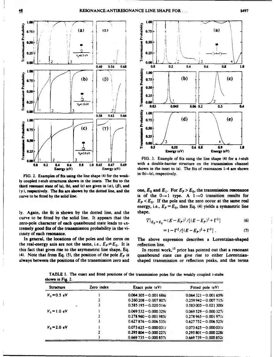
48 RESONANCE-ANTIRESONANCE LINE SHAPE FOR ... 8497
(a) ( a) o.Ts- I I (a)
~0.50 A015 0.25
0.4 0.5 0.6:9- 0.01 0.2 (b4 0.6 - 0.8 1.0
1.00f 1.00
0.75- f() () 0.7S- (C)6 00 0.50
2_l5 Von,.5 I. C 0.00 0.2 -060.0.3-.
1 .oo__________ 0___ 05 .2 0 ~ . 0.75- d (e)2 I
V0 (Y) 0.50 0.. 0.4 0.8 09 iO
0.0 -3l /
o.s ) 13 Energy (ev) Energy (eV)
0 __ . ____2 _3 3 ____FIG. 3. Example of fits using the line shape (4) for a t-stub
0.0 0.2 0.4 0.6 0.2 1.0 0.6 0.67 0.69 with a double-barrier structure on the transmission channelEnergy (eV) Energy (eV) shown in the inset to (a). The fits of resonances 1-4 are shown
FIG. 2. Examples of fits using the line shape (4) for the weak- in (b)-(e), respectively.
ly coupled t-stub structures shown in the insets. The fits to thethird resonant state of(a), (b), and (C) are given in (a), (p), and(y), respectively. The fits are shown by the dotted line, and the one, E0 and E 1. For Ep > Eo, the transmission resonancecurve to be fitted by the solid fine. is of the 0--. 1 type. A 1 -.*0 transition results for
Ep < E0. If the pole and the zero occur at the same realenergy, i.e., E- E0, then Eq. (4) yields a symmetric fine
ly. Again, the fit is shown by the dotted line, and the shape,curve to be fitted by the solid line. It appears that the 'IPE0(-p22(E E)+~ (6)zero-pole character of each quasibound state leads to ex- ~ E E-E)/(EE)Ftremely good fits of the transmission probability in the vi- strutur n(E-Ep 2+ ho21 (7)cinity of each resonance.
In general, the locations of the poles and the zeros on The above expression describes a Lorentzian-shapedthe real-energy axis are not the same, i.e., Ep-#E 0 . It is reflection line.this fact that gives rise to the asymmetric line shape, Eq. In recent work,(5 price has pointed out that a resonant(4). Note that from Eq. (5), the position of the pole Ef is quasibound state can give rise to either Lorentzian-always between the positions of the transmission zero and shaped transmission or reflection peaks, and the terms
TABLE I. The exact and fitted positions of the transmission poles for the weakly coupled r-stubs
shown in Fig. 2.
Structure Zero index Exact pole (eV) Fitted pole (eV)
V 0=0.S eV 1 0.064 305 -0.001 686i 0.064 321 -0.001 659i2 0.260 208 -0.007 807i 0.259 942 -0.007 715i
S3 0.585 195-0.020514i 0.=583=0052-E.021 300i
Vr = 1.0 eV 0.069532-0.000329i 0.069529 0.000 327i2 0.278 960-0.001 985i 0.278 965 -0.001 971 i3 0.627 876-0.006 535i 0.627 752 -0.006 525i
V0 =2.0 eV I 0.073 625-0.000031 i 0.073 625 -0.000031i2 0.295804-0.000227i 0.295801-0-000228i3 0.669 735 -0.000 857i 0.669739-0.000 852i
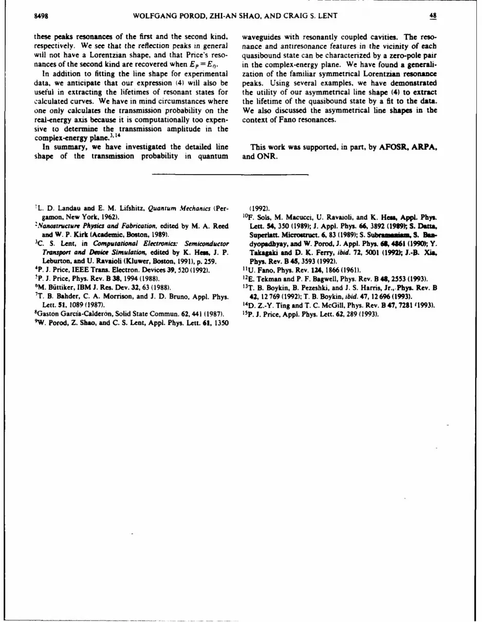
8498 WOLFGANG POROD, ZHI-AN SHAO, AND CRAIG S. LENT 48
these peaks resonances of the first and the second kind, waveguides with resonantly coupled cavities. The reso-respectively. We see that the reflection peaks in general nance and antiresonance features in the vicinity of eachwill not have a Lorentzian shape, and that Price's reso- quasibound state can be characterized by a zero-pole pairnances of the second kind are recovered when EP = E0 . in the complex-energy plane. We have found a generali-
In addition to fitting the line shape for experimental zation of the familiar symmetrical Lorentzian resonancedata, we anticipate that our expression (4) will also be peaks. Using several examples, we have demonstrateduseful in extracting the lifetimes of resonant states for the utility of our asymmetrical line shape (4) to extractcalculated curves. We have in mind circumstances where the lifetime of the quasibound state by a fit to the data.one only calculates the transmission probability on the We also discussed the asymmetrical line shapes in thereal-energy axis because it is computationally too expen- context of Fano resonances.sive to determine the transmission amplitude in thecomplex-energy plane. 3'"
In summary, we have investigated the detailed line This work was supported, in part, by AFOSR, ARPA,shape of the transmission probability in quantum and ONR.
L. D. Landau and E. M. Lifshitz, Quantum Mechanics (Per- (1992).gamon, New York, 1962). 'OF. Sols, M. Macucci, U. Ravajoli, and K. Hess, Appl Phys.
-Nanostructure Physics and Fabrication, edited by M. A. Reed Lett. 54, 350 (1989); J. Appl. Phys. 66, 3892 (1989); S. Datta,and W. P. Kirk (Academic, Boston, 1989). Superlatt. Micro'truct. 6, 83 (1989); S. Subrammiam, S. Bow
3C. S. Lent, in Computational Electronic±. Semiconductor dyopadhyay, and W. Porod, J. Appi. Phys. 68,4861 (1990); Y.Transport and Device Simulation, edited by K. Hess, J. P. Takagaki and D. K. Ferry, ibid. 72, 5001 (1992;, J.-B. Xia,Leburton, and U. Ravaioli (Kluwer, Boston, 1991), p. 259. Phys. Rev. B 45, 3593 (1992).
4p. j. Price, IEEE Trans. Electron. Devices 39, 520 (1992). 11U. Fano, Phys. Rev. 124, 1866(1961)."5P. J. Price, Phys. Rev. B 38, 1994 (1988). 12E. Tekman and P. F. Bagwell, Phys. Rev. B 48, 2553 (1993).IM. Biittiker, IBM J. Res. Dev. 32, 63 (1988). 13T. B. Boykin, B. Pezeshki, and J. S. Harris, Jr.,.Phys. Rev. B7T. B. Bahder, C. A. Morrison, and J. D. Bruno, Appl. Phys. 42, 12 769 (1992); T. B. Boykin, ibid. 47, 12 696 (1993).
Lett. 51, 1089 (1987). 14D. Z.-Y. Ting and T. C. McGill, Phys. Rev. B 47, 7281 1993).'Gaston Garcia-Calder6n, Solid State Commun. 62, 441 (1987). i5P. J. Price, Appi. Phys. Lett. 62,289 (1993).9W. Porod, Z. Shao, and C. S. Lent, Appl. Phys. Lett. 61, 1350
Spatial density of lines exposed in poly(methylmethacrylate) by electronbeam lithography
,iaokang Huang, Gary H. Bernstein. and Greg Bazan/)coartmen Ert Electrwai lElee'rink. L ,'zucrs:tv Otf A.tre Daunt. .\Oire Dame. ?inaiana 46556
Davide A. HillDepartmengt v Chemicai Engineering. Lnivervtv ot Votre Dame. Votre Dame. Indiana 46556
SReceived 30 September 1992: accepted S February 1993)
In this article we report the experimental investigation of the density of patterns exposed withelectron beam lithography (EBL). A linear relationship was found between the minimum widthof poly(methylmethacrylate) (PMMA) walls and the given resist thickness (height of thewalls). Below the minimum width. PMMA walls become wavy or fail due to the internalstresses caused by PMMA swelling during development. Previous research pertaining toproximity effects at feature sizes and spacing below the 0.25 uim range is limited. We haveexpenmentally investigated proximity effects in very-high-density gratings in the pitch rangefrom 50 to 330 nm. The relationship between electron beam dose and grating pitch, whereproximity effects during electron beam lithography play a major role, was achieved. By fittingthe experimental results with a triple Gaussian model, the contributions of the different electrondistmbutions in proximity effects were determined. It was found that fast secondary electronsdominate the proximity effects in the range we studied and they limit the density of patternsfabncated by EBL.
I. INTRODUCTION Sub-50-nm pitch semiconductor-metal photodetectorshave also been achieved by Chou et aL4
The fabrication of nanostructures, and in particular Another serious limitation on very-high-density pat-quantum devices, depends on the resolution and achievable terns with electron beam lithography is the proximity ef-pattern density of lithographic techniques. In electron fect. This is due to the distribution of the primary electronbeam lithography (EBL), the lithographic resolution relies beam, forward scattered electrons, secondary electronson that of the electron beam generator and the contrast of scattered in the resist film on the substrate, and backscat-the resist/developer system. Poly(methylmethacrylate) tered electrons from the substrate. It is important because(PMMA) is still the most popular choice of resist for those scattered electrons expose regions of the resist thatnanostructure fabrication because of its extremely high res- are not originally written by the electron beam. For theolution. schematic grating shown in Fig. 1(a), the electron beam
In the lift-off process commonly used in nanofabrica- exposes the pattern on each line. In the ideal case, thetion. PMMA exposed with an electron beam is followed by resulting energy distribution in the resist is very spatiallya develop step, after which the unexposed resist remains on confined [Fig. 1 (b)]. However, the actual energy distribu-the substrate and acts as a shadow for metal evaporation. tion for very-high-density gratings is less distinct,- asFor very-high-density patterns, the remaining PMMA is in shown in Fig. 1 (c), and proximity effects decrease thethe form of a thin wall between the developed lines, which modulation transfer function of the exposure for closelyserves as the spacer between deposited metal lines. Al- spaced patterns. [the modulation transfer functionthough PMMA is usually considered to be a nonswelling (MTF) is defined in Fig. 1(c).] Assume the peak doseresist, accounting partially for its high-resolution proper- received by each line is E, and the lowest dose received atties. some absorption of developer is necessary to aid in the the areas between lines is E,.. The resolution of gratingsdevelopment process.' A very small amount of swelling depends on the capability of a given developer to distin-can induce internal stresses in thin PMMA walls which guish between E,. and E,. The distribution of electrons inweaken its mechanical properties and cause the deforma- e-beam lithography is complicated by the fact that it de-tion of thin resist walls during development in the fabrica- pends on almost all parameters in lithography, e.g., accel-tion of very close lines. In the limit of very-high-resolution erating potential, beam size. photoresist thickness andlithography, lines are placed so closely together that the type, and substrate properties. Investigations of the energyresist walls can either become wavy, fall over, or fail distributions have been reported elsewhere.-5 ' A doublecompletely. -3 Therefore. the buckling of the PMMA walls Gaussian model has mostly been used for the electronlimits the ultimate density of patterns in the EBL process. distributions.:56 '.11 4 Computer-aided proximity effect cor-Although Chen2 predicted that the limit of line pitch is rection and other methods reducing the proximity effects- 75 nm. our results show that for 100-nm-,hick PMMA during e-beam lithography have been pursued.'- 2 ° Thewalls. PMMA can be as narrow as 20 nm without resist feature size and spacing in most of the published work arefailure. 3 resulting in higher density than expected by them. in the half-micron regime, which is quite useful for fabri-
1739 J. Vac. ScL TecowiO. A 11(4), Jul/Aug 1993 0734-2101/93111(4)11739/6/51.00 1993 American Vacuum Society 1739

1740 Htuang et a!.: Spa~tial density ot tines exp~osed in tMMA ( 4u
"r" '8LE I Experimental parameters.
Expernment Proximitv effect Strength of PMMA
l'~iitern• .\rravs ol graiings Two parallel lines
or gratings
Eidctron dearn sed, Line pitch 50-',30 nm 70-1S0 nm-\cceleraning voltage 50 kV 45 kVResist thickness o0-7O nm 105-180 nm
-7, Developer \iIBK.I1PA M EK M IBK:IPA:MEK.: - 13 . Ob~t 5% MEK) = 13:O.O4(1% MEK)
-=Developer temp. C/ 25..2;Developing time ti-tO s 1Is-aMetal thickness 15 nm 30 nm
Di stance
* ity effect and the strength of PMMA, different processS[ E•parameters were used. A summary of the experimental pa-
S. .. .-. rameters is given in Table 1. The resist thickness in the
* . -,• v c proximity effect measurement was kept to 60-70 nm inSE .) order to avoid PMMA failure during the processes. Grat-
SMTF : - -E •*E. ings with different pitch in the proximity effect experiments
Ossi.... are 3 pm x 3 pm in size and separated by 2 pm with eachother in order to eliminate the proximity effects caused bythe scattered electrons from adjacent gratinp.2 z3
FIG. I. Exposure energy dastmbuion in very-high-density gratings. (a)Schematic of the beanm scan for a grating. b) Energy distmbution in the Iln RESULTS AND DISCUSSIONnear ideal case for the beam scan shown in (a). (c) Actual energy dis-tnbution in sery-highs-density gratings. A. Strength of PMMA
In order to achieve liftoff of evaporated metal films, it iscating ULSI circuits. In this case, backscattered electrons necessary that PMMA walls remain between the developeddominate the proximity effects because of the typically low areas. The width of PMMA walls was determined by mea-beam energies utilized (- 25 keV). The width of the back- suring the spaces between resulting metal patterns afterscattered electron distribution is in the order of the feature liftoff. The undercutting for thin resists was neglected be-size and spacing. However, previous research pertaining to cause it is small for thin resists and high beam energies.proximity effects at feature sizes and spacing below the The height of the walls after development is assumed to be0.25 pm range is limited.•-1 ' the same as the initial resist thickness because the unex-
In this paper, we report the experimental investigations posed PMMA of very high molecular weight has very lowof the density of the electron beam lithography limited by solubility.22 One might suppose that in the case of high-the physical strength of PMMA and proximity effects. density gratings, areas between lines might be partially de-Proximity effects in very-high-density gratings were exper- veloped because of proximity effects. For grating pitchimentally studied in the pitch range from 50 to 330 nm. We larger than 70 nm, we find in the next section thatwill discuss the relationship between electron beam dose EV,/EP < 0.6. For the developer with contrast, y*, largerand grating pitch, where proximity effects during electron than 10, the amount of the resist that is removed throughbeam lithography play a major role. developing is small compared with the original thickness of
the resist, and therefore can be ignored in the final resistII. XPEIMENAL ROCEUREthickness determination.II. XPEIMENAL ROCEUREPMMA can be considered a strong, glassy material after
The EBL system used in this study consisted of an Am- baking. However, during development, the absorption ofray 1400 scanning electron microscope (SEM) with a the developer causes swelling, and internal stresses result inmaximum beam energy of 50 keV and a minimum the deformation of PMMA walls. The wall aspect ratiobeam width of 5 nm using a W cathode, controlled by an (height-to-width) is an important parameter in delineatingIBM PS/2 personal computer interfaced through a Prag- the stability threshold, since a tall, thin wall will bematic Instruments 2201A 16-bit arbitrary waveform strongly susceptible to small dimensional perturbations
genraor.'1Special care was taken to minimize all noise around the erect position. while a short and thick wall willsources. PMMA (950 000 amnu) was spun on Si and be able to sustain a higher degree of swelling before buck-SiO,/Si wafers and baked at 170 °C for 4 h. Mixtures of ling.methylisobutylketone (MIBK):2-propanol (IPA) (1:3) Figure 2 shows experimental results of the minimumwith the addition of 1% and 1.5% methylethylketone width of a PMMA wall achievable for a given starting(MEK) by volume, were used to develop samples. This resist thickness. Error bars represent variations in metalmixture has been shown to have very high development line separation (and therefore wall thickness) over thecontrast properties.:2 For both the experiments on proxim- length of the lines. These data were obtained by smoothly
J. Vac,. Sd Technol. A, Vol. 11, No. 4, JullAug 1993

1141 iuang @I at:. bpatial aensity o0 lines exposed in IMMA 1741
;TPAIGHr IL .
2-0
jNSTAOLE
WAVY WALLS)
X (a)
3 20 40 6 0 80 100 120 140 160 180 200
CttICal Height rimI
FIG. 2. Minimum %idth of PMMA walls achievable vs staning resistthiekness 1 %all heihti)h"
varying the line pitch for a given resist thickness and ob-serving the point at which lines either failed completely orbecame noticeably wavy. The data indicate a direct pro-portionality between critical wall height and width, imply-ing a constant aspect ratio for buckling. The area above thecritical line is the regime in which straight PMMA wallscan be achieved. The area below it is the regime in which (b)
the walls become wavy or fail.The stability of an infinitely long wall of width w and
height h with a rigidly anchored bottom and a top free endcan be modeled with linear plate theory.-' The details ofthe theo.'etical calculation are given in Ref. 25. Accordingto this model, the critical wall aspect ratio for stability,(h/u,). is given as a function of the swelling strain:
"-ht 135 "(I)
where v is Poisson's modulus and c,. is the hypotheticalswelling strain that the wall would undergo if allowed toexpand freely. For (h/v) > (h/w)* the wall will buckle asThown in Fig. 3(a). The bright areas in Fig. 3 are evapo-rated gold. and the dark areas are the areas where PMMA (c)walls stood before liftoff. Equation (I) predicts a linear FIG. 3. Remaining metal patterns after liftoff. (a) Failure of parallel linesrelationship between the critical wall height and width for caused by wavy PMMA walls between them. (b) A typical failure of
a constant c,,. which is consistent with our experimental gratings resulting from PMMA wall swelling and buckling. (c) A 50 nmresults as shown in Fig. 2. From the slope of the line in Fig. grating with straight PMMA walls between lines. Light areas are gold.
and dark areas are the shadows of PMNIA walls which have been re-"2. the critical aspect ratio for stability can be calculated, moved during liftoff.giving (h/w)" = 4.75. Then cs, = 5.1% for v= 0.5 fromEq. (1). This indicates that 5% swelling can lead to failureof PMMA walls with aspect ratio greater than 5.
In making gratings, a set of parallel PMMA walls formsduring development. The buckling of one of the walls can Proximity effects must be strongly considered in the fab-lead to the catastrophic failure of the whole grating, be- rication of very-high-density patterns. It can be expectedcause surface forces can induce cross correlation between that when lines get closer together, the dose needed fordeformation of adjacent structures, producing a pattern of exposure should decrease because interline scattering ofadjacent smusoidal waves 180' out of phase with respect to electrons causes additional energy deposition. Experimen-each other as shown in Fig. 3(b). Figure 3(c) shows a 50- tal results of normalized dose versus grating pitch arenm pitch grating with straight resist walls between lines, shown in Fig. 4 along with theoretical simulations. In the
J. Vac. Sd. TechnoL A. VoL 11. No. 4. Jul/Aug 1993

1742 Huang of aL: Spatial denlity of linel exposed In PMMA 1742
Forward electrons
-• , '• • •. o. iaExpertmenutl data o e,-: ., r.Broad range c'lectron,.
* ~Only forward tlectrona
"Double Gausstian model
O ,Triple Gaustian modei005
SBackscatiered electrons
Pitch of Graitngs torn' Pitch of Gratings turmn
Fin. 4 The relationship between normalized dose and grating pitch Fi i, 5 Interline proximity effects caused by scattered electrons vs pitchDo,,c are normalized to the dose required for the same itnewidih at a oi gratings.pitch of 150 nm
range discussed here. In Eqs. (2) and (3). a, 13, and y arefigure, doses for various pitch values are normalized to that the widths of each Gaussian distribution, and 17 and 77' areneeded for the same linewidth in the !50 nm pitch grating. the ratios of exposures of the second and third term to theThree samples with different doses and development time forward exposure, respectively. According to Ref. 8,were measured. The data of all-three samples are very /3 = 10/m and 71 = 0.8 for 50 keV electrons in solid siliconconsistent. Besides exposure dose, many factors affect line- substrates, a, y, and 17' were chosen for the apparent bestwidth in experiments, such as contrast of developers, de- fit. The dashed line in Fig. 4 shows the calculation in whichveloping time, and temperature. Our results show that al- only the first Gaussian term, that is, only the contributionthough linewidth may change with other factors, their of forward scattered electrons, was considered. Since theeffects on the relationship between normalized dose and width of this term is only a few tens of nanometers, for-grating pitch are small and can be neglected. It can also be ward scattered electrons only cause a short range proxim-seen that normalized dose decreases slowly with pitch until ity effect.about 100 nm when the change becomes rapid. As we will When the second Gaussian term was added in the cal-show, this effect is due to the different distributions of culation (the double Gaussian model), the weak change ofscattered electrons in the resist during exposure. Models of dose over large changes in pitch (solid line in Fig. 4) wasthe exposure energy distribution in the resist employed for caused by the long-range proximity effect of backscatteredfitting the experimental data include the double Gaussian': electrons. The small difference between the dashed curve
2 and the solid curve shows that the proximity effect causedf(r) --I + -exp _-1 -X _--t 1, (2) by backscattered electrons at 50 keV is weak. a =0.037ir ( If + 17)a- ( a-i Jum was used in these two curves. The dash-dot line in Fig.
and the triple Gaussian model": 4 was calculated with the triple Gaussian model. This
I I curve tits the data very well with a =: .029 nim, ,, 0.4f (r) = -- _r 1 -+ exp e xp pm. and 77' = 0.35. We conclude, therefore, that the prox-
a-( " "+17) \ - 1 imity effect from the y-term electrons is very important in
r 11 high-density patterns in EBL. Since these electrons cause-) exp( 0) 3 proximity effects in a broad range relative to the forward-- pscattered electrons, and their sources are still not clear, we
The simulation curves are shown in Fig. 4. In Eqs. (2) and call them simply "broad range electrons.",'3) the first term is used to describe the primary beam and The ratios of the contributions of scattered electronsforward scattered electron distribution The second term from the interline exposures to the total exposure receivedaccounts for the behavior of the backscattered electrons. by each line are shown in Fig. 5 The solid line. the dashedThe third term in the triple Gaussian model is added to line. and dash-dot line correspond to the interline exposuredescribe all other exposures :bat are not included in thc contributions of forward scattered electrons. backscatteredfirst two terms. The third term may result from large angle electrons, and broad range electrons, respectively. Fromforward scattered electrons. secondary electrons, or even Fig, 5 we see that for the interline proximity effects: (i)broad tails in the primary beam distribution .. The resuth The contributions of' backscatiered electrons weakl% de-of Monte Carlo calculations bh Jo\ and Murata c' a:'U pends on the grating pitch because of their wide distribu-clearly show broad tails to the energy distribution due to rion 1U It gim (Refs. 8 and 26)) at 50 ke\ The backscat-fast secondary electrons, which we will sho%% play an tnt iered coefficient is a constant for certain materials when theponant role in proximity effect calculations over the spatial heam energy is larger than 20 keV "Hence the intensity of
J. Vac. Scl. Technol. A. Vol. 11, No. 4. Jul/Aug 1993

1743 Huang et al.: Spatial density of lines exposed In PMMA 1743
As mentioned above, the total dose at the region be-0 3-oim.,n-.o8 tween the electron beam scanned areas increases when
Dul lines are placed closer together. The resolution of gratingsDouble Glaha--0J03m created with EBL depends on how well a developer can
Trnple Gasi,- distinguish between the deposited energy densities betweena.-o029 Pm lines and at the lines. E. and E_ respectively. Figure tca=oo2 pni shows EVE., as a function of grating pitch with different
L.U a40 o,,0 01 Min Gaussian parameters. The dotted line results from the dou-
-) 04 rn. ,i =0 35 ble Gaussian model with the same parameters used in the
calculation of Fig. 4. For 50-nm pitch gratings. the ratio
E.!E. is about 0.98. This small difference between expo-sure energies cannot be distinguished with any practical
,2 0l 0 o ,3 developers, in contradiction to the experimental results.Pitch ofGratizmpi i Therefore, although the double Gaussian model can be
used to qualitatively simulate the normalized dose chang-
FIG. 6. E-E. vs grating pitch E is the Iovest exposure energy received ing with grating pitch, it fails in predicting the density andin the areas between lines. E. is ine maximum exposure energy received resolution limitation in electron beam lithography at theseby each line very small dimensions. The solid line is calculated with the
triple Gaussian model with the same parameters that fit theexperimental data in Fig. 4. It can be seen that EIE,
the backscattered electron distribution for 50 keV is much approaches unity when the grating pitch decreases.
lower than for 20 keV because it spreads much further. E,/E, = I means that the grating patterns are completely
Therefore, for high-density patterns, the proximity effect of washed out because of the proximity effects. For 50-nm
backscattered electrons is like a weak background. It can pitch gratings, EIE,,zO.87. The contrast, )y*, of our de-
be ignored in the total exposure because the contribution of veloper ( 1.5% MEK) is larger than 10 and corresponds to
backscattered electrons is less than 2% and much smaller D,/D!_z0.8,z: where D, is defined as the critical dose be-
than the contribution of the broad range electrons in the low which the resist is not developed at all, and Df is the
whole pitch range over which our calculations were per- dose above which the resist is totally dissolved. (Note that
formed. (ii) The effect of forward scattered electrons is not the exposure energy E is proportional to the received dose
important until the pitch of gratings approaches the width D so contrast curves yield useful information about the
of its distribution. Their effect increases dramatically when limits on absorbed energy.) The resist will be partially dis-
the pitch is smaller than 50 nm. Therefore, the proximity solved when the dose is less than Df, but greater than D,.
effect of forward electrons will limit the resolution of elec- This means that the height of the PMMA walls was de-
tron beam lithography. (iii) Broad range electrons domi- creased for 50-nm pitch gratings during development be-
nate the proximity effect in the pitch range from 50 to 350 cause of partial developing. Since the initial PMMA thick-
nm or even larger in our experiments. This range is on the ness in our case was 60-70 nm. the height of remaining
order of feature sizes of quantum devices and ULSI cir- PMMA walls is assumed to be larger than 40 nm. which
cuits. Therefore it is very important to include this term in we have found is sufficient for good liftoff of 15 nm metal
the proximity effect correction. Since the contribution of patterns. This also shows that the development is very crit-
the broad range electrons to the total exposure is larger ical in making very high density patterns: a slight overde-
than 200,- when grating pitch is less than 50 nm, their velopment may cause the PMMA walls to be dissolved.
limitation on the resolution and density of electron beam From Fig. 5 we see that forward scattered electrons.
lithographically defined patterns cannot be ignored. including fast secondary electrons, cause the proximity ef-We further consider here the role of fast secondary etec- fects to dramatically increase when grating pitch approach
trons in proximity effects. Fast secondary electrons have a a. the width of the distribution of forward scattered elec-complicated distribution: it is a narrow peak with a wide trons. Thus the resolution of EBL can be improved when ashoulder.5. The width of the narrow peak is about 10 nm decreases. This is clearly shown by the dashed line (a = 20in free-standing resist. Its role in proximity effects was in- nm) and the dash-dot line (a = 10 nm) in Fig. 6. Thiscluded in the forward scattered electrons5 which are de- requires using a very-high-energy system with a non-scnbed by the first term of the double or triple Gaussian Gaussian-shaped beam or a resist that depends less on ioAmodcls. However. the proximity effect caused by the wide energy electrons in forward electron scattering. Assumingshoulder was neglected b. previous researchers. From Ref. a = 10 nm for a %erY high-resolution electron beam. a grat-5 we note that the half-width of the shoulder is about 100 ing %nith 20 nm pitch can be expected using a deseloper
nm and is on the order of the distribution of the broad with the contrast -4 = 10. as shown in Fig. t. This agreesrange electrons. Therefore. it can be concluded that fast with predictions of Joy' that 1(0 nm represents the ultimatesecondary electrons are part of the broad range electrons, resolution for PMMA as an electron beam resist Our re-but the% are not the oni. part Therefore. the fast second- suits restate those of Joy that the narro% peak of the en-ary electrons introduce both short- and long-range prox- ergy deposited b\ secondary electrons i, practically flat outimitv effects. and thereb% limit the resolution of EBL to a distance of 5 nm. and therefore so , o, in contrast
J. Vac. Sci. Technol. A, Vol. 11. No. 4. Jul/Aug 1993

1744 Huang of at: Spatial density of lines exposed in PMMA 1744
(over the peak) as to be indistinguishable to developers ACKNOWLEDGMENTSwith reasonable contrast values.
We saw that the pattern density is also limited by the *rhe authors thank D. T, Leightot, for helpful discus-failure of PMMA walls. As discussed above, the lower the 'ions, and S. Subramaniam for help in sample preparationachieved thickness of the PMMA walls, the closer is the and useful discussion. We gratefully'acknowledge IBM,achievable line spacing. However. the resist thickness can- AFOSR, ONR, and the University of Notre Dame fornot be lowered arbitrarily because, for good liftoff. the re- their support of this research. D. A. If. thanks the Donorssist thickness should be about three times the metal thick- of the Petroleum Research Fund, administered by theness, which depends on the ultimate desired device American Chemical Society, for partial support of this re-char.-cteristics. According to Fig. 2. 10 nm spacing be- search.tween metal lines can be achieved with 40-nm-thickPMMA, and is sufficient for successful liftoff of 10 to 15-nm-thick metal lines. Therefore, we conclude that the lim-its to the density of metal lines due to the proximity effectand the strength of PMMA walls are consistent for the 'A. Weill. in rhe Phvsics and Fabrication of'Mficrostruciures and Mr-achievement of lines with pitch as small as 20 nim. crodevices. edited by M. J. Kelly and C. Weisbuch (Springer. New
York. 1986). p. 51,-Z. W. Chen. in Adiances in Electromnics and Electron Phvsics, edited by
IV. SUMMARY Peter W Hlawkes (Academic. New York. 1192), Vol. 83, p. 187'X Hluang, G. Bazan. D. A. Hill, and G. H. Bernstein. J. Electrochem.The proximity effects in electron beam lithography were . 139. 2952 192)
experimentally investigated with different grating pitch. 'S. Y. Chou, Y. Liu. and P. B. Fischer, IEDM 91, 745 (1991).The results were successfully simulated with a triple 'D. C. Joy. Microelectron. Eng. . 103 (19831.Gaussian model. Proximity effects caused by backscattered K. It. P. Chang. D. Vac. Sci. Technol. 12. 1271 l1575)electrons were insignificant in our case because of their ( 1981).wide distribution. Forward scattered electrons were very 'R. M. Mankiewich, L. D. Jackel, and R. E, Howard, J. Vac. Set.important when the grating pitch was about the width of Technol. B 3. 174 (1985).this electron distribution. Broad range electrons, described 'S. J. Wind. M. G. Rosenfield. G. Pepper, W. W. Molzen, and P. D.
Gerber, J. Vac. Sci. Technol. B 7, 1507 (1989)by the third term in the triple Gaussian model, dominate "R. J, Bojko and B. J. Hughes. J. Vac. Sci. Technol. 0 8, 1909 (1990)the proximity effect in the pitch range from 50 to 350 nm. "S. A. Rishion and D. P. Kern. J. Vac. Sci. Technol. B 5, 135 (1987).Secondary electrons cause both short- and long-range 12A. S. Chen and A. R. Neureuther. J. Vac. Sci. Technol. B 3, 148proximity effects. Their effects can be included in forward (1985).scattered electrons as well as broad range electrons. Their "A. Misaka. K. Harafuji. and N. Nomura. J, Appl Phys. 68. 6472
(1990).limitation on the EBL resolution cannot be ignored. "G, Owen. 3. Vac. Sci. Technol. 1B 8. 1889 (1990).
Upon exposure to suitable solvents, such as common "G, Owen and P. Rissman, J. Appl, Phys. 54, 3573 (1983)developing and rinsing solutions, narrow PMMA walls "S W. j. Kuan, C. W. Frank. Y. H. Yen Lee. T. Eimon. D. R. Alice. Rwere found to become unstable as a result of two effects: F W. Pease, and R. Browning, 3. Vac. Sci. Technol. B 7. 1745 (1989)(1)swer ling, f nd to becomeanteabl surac oresut oetwoefen s a"D. G. L. Chow. J. F. McDonald, D. C. King. W. Smith. K. Molnar.)swelling, and (2) lateral surface forces between adja- and A. 1, Steckl. 1. Vac. Sci. Technol. B 1, 1383 (1983).cent structures. We investigated the relationship between "R. L. Kostelak. E. H. Kung. M. G. R. Thomson. and S. Vaidya. J. Vacminimum line spacing and maximum PMMA thickness for Sci. Technol. B 6. 2042 (1988).EB3L fabrication using a high contrast developer. We also '"E. Nishimura. T. Takigawa. T, Abe. and Y. Katoh, J. Vac. Set. Tech.
nol. B 4. 164 (1986)showed experimental evidence that supported our predic- "R. C. Frye. J Vac. Sci. Technol. 1 9, 3054 (1 Q 11,tions, thus demonstrating the existence and severity of "'G. Bazan and G 11 Bernstein. J. Vac. Set Technol A II. 174ssuch instabilities in nanolithography. (1993)
From our calculation of EEE as a function of grating 2-G. H. Bernstein. D A Hill, and W .P. Lii. J AppI Phy% 71. 40.6the turipleGaussian mdela a 20-nmtio po grati (1992)pitch with the triple Gaussian model. a 20-nm pitch grat- 'K. L. Lee and H. Ahmed. I Vac. Set. Technol. 19. 946 (1981)ing can be expected using a very high-resolution electron "S P Timoshenko and J. M. Gere. lTheorv of Elasie Stablhey. 2nd edlbeam generator and high contrast resist/developer system. (McGraw-Hill, Ne% York, 1%611. p, 363.The closest spacing between metal lines can be as narrow "'D, A. Htill, X. Huang. G. lasan. and G. H. Bernstein. J AppI. PhyvThe losst pacng btwen mtallins ca beas arrw -72, 4088 (19Q2)as 10 nm for 10 to 15-nm-thick metals, implying that 20 7J. S. Greene0ch8 J Vac. SC Technol. 16. 174 (1979).nm gratings with 10 nm linewidth and 10 nm line spacing 'L. Reimer. in Scanning Electron Microscops (Sponger. New York.are achievable. 1985). p 137
J. Vac. Scl. Technol. A. Vol. 11. No. 4. Jul/Aug 1993

Electron beam lithography over large scan fieldsGreg BazAna) and Gary H. BernsteinDepriment of Electicai Engineenng, Lnwerstwv o0 .otre Dame. Aotre Dame. Inaiana 4'6556
(Received 30 September 1992. accepted 18 January 1993)
We have developed an advanced, research-onented electron beam lithography system using athree channel arbitrary wave form generator and a scanning electron microscope. The system iscapable of exposing pattt.ns with features less than 100 nm over scan fields greater than 1.0 mm,as well as features less than 20 nm in smaller scan fields. Other system features includecapabilities for registration and for generating exposure matrices for evaluating new electronbeam resists and optimizing exposure parameters. We report the details of the system and showresults made possible by our system.
I. INTRODUCTION tive exposure parameters could be stored for future analy-sis and images printed and saved easily.
For more than a decade, intense effort has been put The most common method used to convert a SEM to antowards the construction of dimensionally confined sys- EBL system incorporates a computer fitted with twotems for the study of quantum effects in mesoscopic digital-to-analog converters (DACs) whose outputs arestructures.' To this end, simple devices have been con- connected through amplifiers to the SEM scan col Morestructed using processing methods similar to those used to sophisticated conversions involve computer conrolledfabricate GaAs meal-se-mconductor field effect transistors beam blanking and stage movement Nabity and(MESFETs). To study quantum effects, minimum feature Wybourne 9 give an especially thorough review of the de-sizes within these structures must be less than IAm, and sign issues involved in a SEM-bsed EBL system. In alloften less than 100 nm 3.24 Several approaches for fabricat- cases, the computer controls the beam position by the ap-ing structures with features less than 50 nm have been plication of voltages via the DACs. Ideally, the beam po-implemented,5- 7 but none combines the versatility and res- sition resolution of these DAC-based systems is strictlyolution capabilities of electron beam lithography (EBL) limited by the DAC resolution. Earlier designs used 12-bitsystems. X-ray lithography systems are capable of such DACs while most current systems use 16-bit DACs and,resolution but are not readily available. Some commercial presumably, future systems will have even higher resolu-EBL systems have the resolution necessary to produce the tion. When 16-bit resolution is used, the beam can be po-required sizes yet are not readily available due to the their sitioned anywhere on a 65 536 by 65 536 point grid. Thecost. Using scanning electron microscope (SEM)-based spatial resolution of this grid is determined by the SEMEBL systems can provide a low-cost, versatile, research magnification. To move the beam, successive positions inexposure tool whose only disadvantage is throughput. the form of digital integers or pixels are input to the DACOther cost effective methods include the modification of at a predetermined rate calculated from the feature size,scanning tunneling microscopes (STM),8 but this technol- the exposure dose, and the beam current. This rate is cal-ogy currently is limited by the overhead exposure time and culated to include the exposure time at that location as wellthe small exposure area. as any overhead time necessary to account for scan coil
Several EBL system designs have been implemented and settling.9-1i
described by others.9-20 However. our work extends the The minimum feature size of such systems is not onlyutility of this technique into the regime of very large scan determined by the DAC spatial resolution, but also by thefields with nanometer resolution. Our motivation behind temporal resolution. For systems with poor temporal res-the development of this system was the ability to fabricate olution, a low exposure dose can only be achieved-by hav-nanostructures and nanodevices incorporating all exposure ing fewer pixels in an exposure to result in the desired dosesteps (mesa. contacts, gates, bonding areas) into one tool at a given magnification and beam current. In this case, ifas well as gate level exposure for quantum based circuit the pixel spacing is large compared to the beam diameter aarchitectures."' Also recent optical expenments require discrete pixel exposure will result. Therefore, if faster pixelnanostructures in large scan fields due to the difficulty in outputs are possibre, pixels can be placed closer together onfocusing lasers onto small areas :2 We designed our system the grid resulting in smoother lines, more uniform expo-with three specific goals. The first was to build a system sure doses, and improved overall performance.capable of exposing any arbitrary pattern with a resolutionless than 100 nm over scan fields as large as 1.4 mm. The II. SYSTEM OVERVIEWsecond was to allow the exposure tool to perform accurate Control of the lithography system is achieved throughpattern registration of 100 nm over scan fields as large as an in-house software program: 3 written specifically for
4 mm Finally, the system was designed so that cumula- electron beam lithography. The program we developed iscapable of generating two types of files: layout exposure
kuihmo to wbim axmponduwe shovid be adrdmmd. and alignment (registration). Each file must be assigned a
1746 j. Vwe. ML TesmeL A 11(4), JuIVAug 1693 0734-2101/93/11(4)/1745/1/11.00 e, 193 Anmerican Vacuum Society 1745

1746 G. lSm sl W G. H. @ernstein: Electron oesam athOgreony over argo scan 'aeola
- ten source. electrostatic beam blanker, and a Robinsoncliffw hackcauttered electron detector Such a large acceleration
potential gives nse to a wide backscattered electron distn-hution in the resist. thus reducing proximity effects during
-eU a • •-WA PC -• the exposure of dense lavouts< The Robinson backscat-T'~ tered electron detector is used dunng the registration pro-
cess to image marks through the resist. Also connected tothe SEM is a Keithley 614 electrometer used to measure
sm, =mew beam current collected in a Faraday cup mounted to thesample holder
am"--'_-__,_ - The beam position and blanking are controlled by a- 1_ 4 Pragmatic Instruments Model 2201A high-definton arbi-
S"• ; * 79k trary wave form generator (AWG). Current advances inA • usEW wave form generation electronics- 2b7" make the use of a
high resolution AWG a superior choice for controllingSEM-based EBL systems. The 2201A is a three channel
________ wave form generator with each channel capable of gener-"" _ ----- NNW -' M ating a wave form with a maximum lengh of 65 535 san-
pies and sampled at a selectable rate from 0.100 Hz to2.000 MHz with four-digit resolution. Each wave form
Fia. I Scie dmpW auof emii- bm btiowbpay ,sm. sample has 16-bit resolution vwthin a selectable voltagerange from 0.01 to 10.2 V with four-digit P oaad. Theselectoble clnne amplitude is extrumely muf fw SiE
magnificaon which is used to determine the scan field by whom scan ampliders compensate for the of mascro-the relation that a SEM magniication times the sca field FraPh0L By scalami the output of the 2201A -m - ao4y,equals a system constant. Our system constant has been the SEM san amplifier ratio can be balanced rameing in aat 140 000 where the scan field is in units of microns. Hay- square scan field. Each channel also has a synchroniuationing such a large system constant allows for the possibility output which is used to monitor the end of wave formto expose patterns over 7 mm. Both files allow for an ex- generation, to provide the pulse signals needed for regis-
eto occ i the b c a tration, and to control the beam blanking. The three wavepos~eform outputs are connected to the SEM with channel 1specified. A layout file can consist of dot, line, and areaexposures defined as a set of primitive shapes. Currently controlling beam blanking, and channel 2 and 3 function-
the set of shapes includes dot grid( angled fines, grat, ing na analog outputs to control the horizontal ad veticalgrids, nngs, rectangles, parallelograms, and triangles. The beam positions. We refer to channel signal outputs asregistration process involves continuously scanning or i11- BBK, XSCAN, and YSCAN, respectively, and channelaging any features designated as the alignment marks. synchronization outputs are referred to as BBKSYNC,These features must be positioned at the corners of a rect- XSYNC, and YSYNC. respectively.angle so that adjustments can be made to reduce rotationalu The Quantel Crystal Digital Image Processor is used tohorizontal. and vertical overlay errors as well as to select capture video information from the SEM. To capture ima-the correct magnification. These marks are scanned simul- ages, the image processor requires video input as well astaneously or individually through a window whose size ca line and frame pulse signals. These pulse signals corre-
be vaned to improve the alignment precision. spond to the end of a horizontal scan and the end of a
A complete schematic diagram of our lithography sys- vertical scan, respectively. To capture an image, the pro-
tem is shown in Fig. I1. The lithography system is con- cessor synchronizes its capture rate to that of the line and
trolled by an IBM PC Model 30/28624 equipped with a 32 frame pulses. When the lithography system is used in an
megabyte hard drive, 4 megabytes of random access mene- imaging mode, the image processor receives line and frame
ory (RAM). a Hewlett-Packard general purpose interface pulses from the SEM and the scanned image is digitized.
bus (GPIB) interface card, and a Computer Boards, Inc. When the system is used in a registration mode, the pro-CIO-DIO24 digital input/output card. The GPIB interface cessor receives line and frame pulses from the 2201A
controls the operation of the wave form generator and the (XSYNC and YSYNC) so that only the scanned areas
CIO-DIO24 card monitors the channel synchronization over the registration marks are digitized.outputs of the wave form generator and controls the syn- Ill LAYOUT EXPOSUREchronization of the beam blanker. Connected to the com-puter through the serial port is a switch box used to direct We have taken great care in designing an EBL systeminformation to a plotter for layouts or to the SEM stage capable of large scan field exposures with nanometer reso-control system. The computer is also connected to a laser- lution. For us, the primary issue for large scan field expo-printer to record SEM exposure parameters as well as the sures is the signal-to-noise (S/N) ratio in the signals usedsize and position of exposures within a layout. Our SEM is to control the SEM scan coils. Noise in the generated sig-an Antray 1400 with a 50 kV acceleration potential, tung- nal can result in a deflection of the beam which depends on
J. Vm. la Tede. A,. VoL 11, No. 4, Jul/Aug 1iin
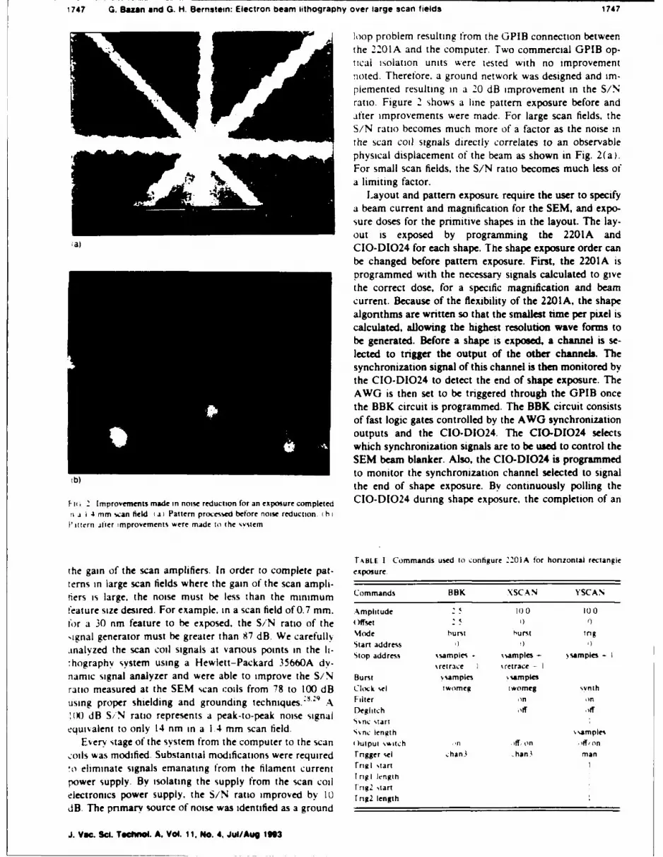
1747 G. Baun and G. H. Bernstein: Electron beam lithography over large scan fields 1747
loop problem resulting from the GPIB connection betweenthe 2201A and the computer. Two commercial GPIB op-tical isolation units were tested with no improvementnoted. Therefore. a ground network was designed and im-plemented resulting in a 20 dB improvement in the S/Nratio. Figure 2 shows a line pattern exposure before andiafter improvements were made. For large scan fields, theS/N ratio becomes much more of a factor as the noise inthe scan coil signals directly correlates to an observablephysical displacement of the beam as shown in Fig. 2(a).For small scan fields, the S/N ratio becomes much less ofa limiting factor.
Layout and pattern exposurt require the user to specifya beam current and magnification for the SEM, and expo-sure doses for the primitive shapes in the layout. The lay-out is exposed by programming the 2201A andCIO-DIO24 for each shape. The shape exposure order canbe changed before pattern exposure. First, the 2201A isprogrammed with the necessary signals calculated to givethe correct dose, for a specific magnification and beamcurrent. Because of the flexibility of the 2201A, the shapealgorithms are written so that the smallest time per pixel iscalculated, allowing the highest resolution wave forms to
be generated. Before a shape is exposed, a channel is se-lected to trigger the output of the other channels. Thesynchronization signal of this channel is then monitored bythe CIO-DIO24 to detect the end of shape exposure. TheAWG is then set to be triggered through the GPIB oncethe BBK circuit is programmed. The BBK circuit consistsof fast logic gates controlled by the AWG synchronizationoutputs and the CIO-DIO24. The CIO-DIO24 selectswhich synchronization signals are to be used to control theSEM beam blanker. Also, the CIO-DIO24 is programmedto monitor the synchronization channel selected to signalthe end of shape exposure. By continuously polling the
Fu 2 Improvements made in noise reduction for an exposure completed CIO-DI024 dunng shape exposure. the completion of an
n ji 14 mm scan field (a) Pattern proc:essed before noise reduction. (h)P ittern itter improvements were made to the svstem
T,1AL1 I Commands used to configure 2201A for honzontal rectanglethe gain of the scan amplifiers. In order to complete pat- exposure
terns in large scan fields where the gain of the scan ampli-tiers is large. the noise must be less than the minimum Commands BBK XSCAN YSCAN
feature size desired. For example, in a scan field of 0.7 mm. Amplitude 05 00 I00
fbr a 30 nm feature to be exposed, the S/N ratio of the offset 2 .,signal generator must be greater than 87 dB. We carefully Miode hurnt hUrut trg.inalyzed the scan coil signals at vaious points in the h- Start address I )I P
" t n s apnStop address ,samples ,samples - ',samples - I:hography system using a Hewlett-Packard 35660A dy- \retrace retrace- I
namic signal analyzer and were able to improve the S/N Burst ,samples ,,amplesratio measured at the SEM scan coils from 78 to 100 dB Clock %el twomeg twomeg svnthusing proper shielding and grounding techniques.182 9 A Filter ,n in
!() dB S/N ratio represents a peak-to-peak noise signal Deglitch ofi off')nc start
equivalent to only 14 nm in a 1.4 mm scan field. snc lengthti samples
Every stage of the system from the computer to the scan Output ,,,tch fnf on )f, on
,:oils was modified. Substantial modifications were required rngger sel ,han3 .han3 man
to eliminate signals emanating from the filament current Trigl startpower supply. By isolating the supply from the scan coil Trig[ length
w lrlit2 stan
electronics power supply, the S/N ratio improved by 10 Vng2 lengthdB. The primary source of noise was identified as a ground
J1. Vic. Scl. TooPnol. A. Vol. 11, No. 4, Jui/Aug 19•3

1748 G. Bazari and G. H. Bernstein: Electron beam 1ithograpny over iarge scan tieas
,,n I
XSCAN
Wigpf XSCAN ardSiti89
YSCAN
I vBmO , Umipin
FIG. 3. Example of the 2201A wave form output when exposing a hon-zontal rectanle. Shown here is an example of three passes across therectangle. YSCAN tnggers BBK and XSCAN. Notice the beam is off (a)dunng the retrace of XSCAN. With this. each sample in YSCAN corre-%ponds to one XSCAN across the rectangle. The time scale for BBK andXSCAN is kept constant at 0.5 jAs and the time scale of YSCAN is equalto the total time for one cycle of XSCAN (xretrace + xsamptes). Toensure channel synchronization. YSCAN wave form output begins on itsSECOND wave form sample.
exposure is detected when 0.0 V is read from the triggeringchannel synchronization output.
The commands used to program the 2201 A to expose ahorizontal rectangle are shown in Table I. YSCAN is se-lected as the triggerng chaanel for BBK and XSCAN sig-nals. Figure 3 shows an example of the wave forms pro-grammed to expose a horizontal rectangle from theinstructions in Table I. The rectangle is exposed whenYSCAN is triggered by the computer. As YSCAN is gen-erated, when the second wave form sample of YSCAN isreached, BBK and XSCAN are triggered. This sequenceguarantees that BBK and XSCAN are synchronized to (b)
YSCAN. The end of the exposure is detected by polling FIG Processed backscattered electron images of alignment marks for
Ia) four mark and i h sminle mark scanmYSYNC through the CIO-D1024. When YSCAN waveform output begins, YSYNC changes from 0.0 to 5.0 V. Atthe last wave form sample of YSCAN, YSYNC changes to exposure dose. Because SEM parameters such as focus anda 0.0 V signaling the end of the shape exposure and the astigmatism can dnft. large overhead times can result in2201A is programmed for the next shape exposure. poor exposure conditions for complex. lengthy patterns.
Use of the 2201 A allows us to minimize the total over- We have optimized the software for all line types to takehead time for an exposure. as well as maximize control of advantage of this property When a wave form is calcu-
lated, the 2201A is instructed to load its memory with thewave form samples. Next. a sampling rate is selected foreach memor, location and the wave form is then tnggered
- _ . for output. For the next exposure. instead of loading a newwave form. the start and stop pointers in channel memoryare moved to correspond to the next exposure and tig-
__,_ U //-gered. With the resolution and range of sampling rates. the
exposure dose can he 'aried hv () IQ from one exposure toN" another Such re.olution is needed when attempting to
+ + 1 characterize new resists and developer solutions as well asto optimize et'xrosure parameters
FI. 4 Registration mark layout with definitions Marks are numbered in IV. REGISTRATION.i clockwise pattent A scan of all marks is completed by scanning marks
I. 2. 3. and 4 to order Scannmg of idiviul marks is selected from A We have developed an accurate technique for achieving
menu within the proganm The size cfi the marks is enlarged for clanty pattern registration. relying on the 2201A and the image
J. Vas. eaL Teev.wL A. VOL 11, Me. 4. JwVAug 109g
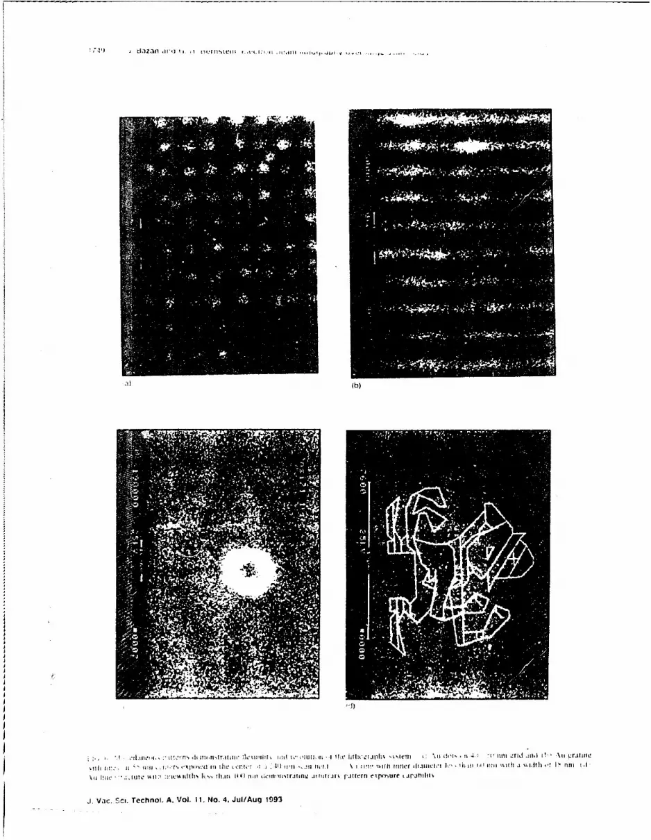
a)(b
'A dt'I')ta ii e lilt i' l l,' 4 1t, j 1% ý j~ jm
I 1 fill] Il~ )'' l 1110 h I. T - - I - I 'l l -- 11 111-1, u\s I wpi uiti Inneir Iimn t.isi Iil ill iii r %~i m lu I 4 ~ikfh qi Iý riim t
.j. Vaic. Sci. Technol. A. Vol. i I. No. 4. Jul/Augj 1993

* -~.~..aaas .. u j. . owibwi..l~ulrw ueain iitnoqrapnV Over iarqe scan 11006 7s
jai (a)
(b)
\i Ii, r.'ira phs 1 1f ule pat tern-, e x x ied i i th tic enter anid hi Iat Fi(,. S. Magnifiied view o1 ines in Fig. h)i a) Vertical grating antd in)wi a -m can teld .poke pattern demnonstrtining kleures under lIM nm in ai 1.0 mrr s an
necldý
V. RESULTSprocteesoir I hec 221)A is used to cont roli the aicquiisitton ,,tmi ait fsa ilsMte [ lie, proces-sor ~tich thiat onils the informiatton We have tested ou~rsyemia a yofcntid.ýcanncti~ l!"0111 il e AIienment inarks, is twitized. rile %vi exposing arbitrary patterns with many exposure doses.
Iroiiii' "~nas o th 21)1A ae cnicurl t eru- Studies investiga ting the properties of poly(methyl-
.ite line and tramne pukse sigtials with otie framei consisting rehcvae P M)'adcagsi xds 2 hv'I41W te1s of iJlco intormation. Shown in Ftc. 4. our been performed using this system. For this work, exposures
-Cchilkiti Inoke scnnig oe iarkor can -ne bur were performed at 50 kV on thick silicon substrates withechniuuc~~~~~~~~~~~ Miosssann n ako cnln!tu O-nm-thick PMNIA of molecular weight 950 000 a.m.u.
ýnirks -i:tiultaneoUSlV. rhe four-mark ,can can he used ito baked for 10 miii at 170 'C using a hot plate. Developmentor.rect toationai errors while single mark -scans~are used was performed at 21 TC for 15 s-in a 1:3 mixture of methyl
7. otrc:i miL'ntification errors as well a,, horizontal and isohutyl ketone: isopropanol with 1%"e methyl ethylcrul Islaezens.Once at mark his been Scanned. the ketone. Metal films, of' \u and Ti/Au were evaporated at
idco~ :worniaition is :ollected h% the tlrocecssor And Lti'- niormal incidence in an ciectron beam evaporator. Lift-ofras ed I ý.rnres it:Ný 1irLIle anid nititipie mat~rk casarv %%as performed h%~ oakiniz in acetone tor 2 to 3 min.
noi~c Hz ti [-le superimposed dark areas in the .\t conventional scan fields around 250 ptm dots ap--*:,inteu mau," ire achieved throuceh heani lNatikinU atnd proximately 13 nlm in diameter ssere fabricated. 14 Some of
c .c -uiaes dutring alignment. Yoi iruprose reL'istratioii our results demonstratingv the flexibility of the system. as.cctiurac\ tie ,lie of thle scan wvindows can he scaled. re- well as resolution. are shown in Fie. ti, Fivure 7 s'hows the!itimL !t nt enitied vtew oft thle recistration mark a.me line pattern exposure at the center -and top edge (if a
ij. Vac. Sci. Technol. A, Vol. 11, No. 4. Jul/Aug 1993

1751 G. Bazan and G. H. 8ernstein: Electron earm itthoqrapnv over large scan fields 1751
1.0 mm scan field. Figure S shows mecnatritmel wl ol'the ,erff, A
vertical grating and sproke pattern ait Pie cdie of' the 1,Il IIIII
mm scan field demonstratingt wiih te.suttito, features in HUMll ltltIII hIlarge scan fields. In Fig. 7(h) \%e ,ee inat the innermnot n - . Iring is displaced in the ",crtical direction. Mitchli is an et\-
ample of the efrects of scan coil settling. 'he inner most I -rint
ring is drawn first in this pattern. t )nee the scan coils hae"
•ettled, dhe remainint pattern is exposed without any no-iceable errors. Such errors are corrected h\ choice of pat- .
scan field: 1.0 mmAtmqerw Mt1lcS t wo m - 10l hrw
b[FiG. to. Exposure pattem used to determine registratkio accuracy. Thedark lines of patterns A and B were fabricated first. Having aligned the
a[] sample, the mirror image of patterns A and B was then fabricated and the
registration accuracy determined.
exposure pattem(horlzontal and
m m mlm mvertical)
(a)
lb)
Fl(). 4 Ftposure pattern utsed to in'e.nmiate the line width variationacross a 1.0 mm scan field. The pattern was exposid both horizontally and (b)
%ertically Over 40 micrographs were taken o'f fabricated lines. Micro. Flo 11. Micropaphs of alignment results for patten A ta) and patterngraphs ia) and tb) correspond to location of boxes in figure drawn. R i i. 1lcat in the center f th e a ieldr
jB .hI of Fig. tc located in the center of the scan field.
S~J. Vac. Sd. TcthneL. A. Vol. 11. No. 4, Jul/Aug 1993

1752 G. Bazan and G. H. Bernstein: Electron beam lithography over large scan fields 11i0d
tern order and addition of delays into the 2201 A program- 'G Bernstein and D. K. Ferry, Superlatt. Microsuctures 2, 373
ming sequence. To test line width variation over a 1.0 mm (1986).scan field, the pattern in Fig. 9 was exposed. The line van- N. Giordano,. Phys. Rev. B 22. 3635 (1980).
scan'E. H. Anderson. C. M. Horwitz. and H. I. Smith. AppI. Phys. Lett. 49.ation was estimated to be 5 nm for 65-nm-wide lines. A ,,74 (1983).
more accurate investigation would require micrographs D. C. Flanders. Appl. Phys. Lett. 36. 93 (1980).
with more detail which, at this time, are currently not 'M. A. McCord and R. F. W. Pease, J. Vac. Sci. Technol. B 6C 293
available. To test the registration accuracy, the double ex- k 1988).pJ. C. Nabity and M. N. Wybourne, Rev. Sc,. Instrum. 60, 27 (1988).
posure pattern in Fig. 0l was used with our best results "S. Thorns, S. P. Beaumont, and C. D. W. Wilkinson, J. Vac. Sci.
shown in Fig. 11. We believe we have achieved an overlay Technol. B 7. 1823 (1989).
accuracy of less than 100 nm. 'C. C. Andrews and W. P. Kirk. J. Vac. Sci. Technol. B1, 1858 (1990)."ýA. J. Speth. A. D. Wilson, A. Lern, and T. H. P. Chang. J. Vac. Sci.
V. SUMMARY Technol. 12Z 1235 (1975)."J. Bellessa, F. Carcenac, A. lzrael, H. Launois, and D. Mailly, Micro.
We have shown that using an AWG to control a SEM Elec. Eng. 6. 175 (1987).for EBL can provide a versatile nanolithographic exposure "S. Mackie and S. P. Beaumont, Solid State Technol. 25, 117 (1915).
tool capable of large scan field exposures. With the fiexi- 15B. L. McIntyre and C. L. Dennis, Appl. Opt. 27, 196 (1988)."`B. McIntyre. R. Perman, and B. Gold, Res. Dev. 31, 44 (1939).
bility of the 2201A, we are able to precisely control the 7,C. F. Cook, T. F. AuCoin, and G. J. lafrate, Solid Smt. TechmaL 23,
exposure dose, accurately position the electron beam, and 125 (1985).maintain beam position as well as control the image pro- liC. P. Umbach. A. N. Broers, R. H. Koch. C. G. Willam, and IL. B.cessor to facilitate device registration. The 16-bit resolution Laibowitz, IBM J. Res. Dev. 32, 454 (1988).
in voltage and four-digit resolution in sampling rates a- "'A. Muray, M. Issacson, 1. Adesida, and B. Whitehead. J. Vac. Sci.Technol. B 1, 1091 (1983).
lows for optimal ontrol of exposure dose. The variable 2°A. N. Broee J. M. E. Haper. and W. W. Mokem, Appi. FhM Lamoutput of the wave form generator also simplifies the ad- A, 392 (197).justment of scan field aspect ratios. We have shown that we "C. S. Lent, P. D. Toupw, W. Porod, and G. H. Uez2 , lamch-are capable of exposing patterns in large scan fields with nology (to be publihed).
nanolithographic features. Having the flexibility to pattern 2B. McCambe (private oamumcatii)."2Turbo Pacal versam 5.5, Barland lnternatinaaL
the fine structures as well as other device features in one 24A high speed computer is not necasary became the timing is per-
system reduces the overhead associated with device design formed by the high speed electronics of the AWO.
and fabrication. -"X. Huang, G. Baziu, G. H. Bernstein, and D. A. Hill J. Vac. Sci.Technol B (to be published).
ACKNOWLEDGMENTS "'A. Pini, Eval. Eng. 30,26 (1991)."J. Sauer, Eval. Engr. 31, 26 (1992).
This work supported in part by IBM, NASA, Air Force 2 R. Morrison and W. H. Lewis. Grounding and &Wekbq in FaciliieOffice of Scientific Research, Office of Naval Research, and (Wiley, New York, 1990).the University of Notre Dame. We thank Xiaokang Huang 29R. Morrison, NoW and Other Interfering Si•hs (WIley, New York,1992).
for the micrographs of exposures ompleted in small scan 3D. A. Hill, X. Huang, G. Bazin, and G. H. Bernstein, J. AppL. Phys.
fields. We especially thank Meinrad Steiner at Pragmatic 72. 4083 (1992).
Instruments, Inc. for his GPIB programming tips. "X. Huang, G. BauAm. D. A. Hill. and G. H. Bernsein, J. Electrochem.Soc. 139, 2952 (1992).
'T. K. Gaylord. E. N. Glytsis. G. N. Henderson. K. P. Martin. D. B. "G. H. Bernstein, S. W. Polchlopek, R. Kamath. and W. Pord. Scan-Walker, D. W. Wilson, K. F. Brennan. Proc. IEEE 79. 1159 (1991). ning 14, 345 (1992)."J. M. Ryan. J. Han. A. M. Kriman. and D. K. Ferry, Proc. SPIE 1284, "G. H. Bernstein, D. A. Hill. and W. P. Liu. J. AppI. Phys. 71. 406639 (1990). (1992).'0. Bernstein and D. K. Ferry. IEEE Trans. Electron Devices ED-3S, "4As imaged with a field emission SEM courtesy of Topoom Technologies,887 (1988). Inc.
J. YVs. S& Teeson. A, Vol. 11, No. 4, Jul/Aug ION3

New technique for computation and challenges for electron-beamlthography
Xiaokang Huang, Greg BazAn, and Gary H. BernsteinDepartment of Electrical Engineering. Univeruity of Notre Dame, Notre Dame, Indiana 46556
(Received 15 June 1993; accepted 20 August 1993)
In this article, the basic concepts of our recently proposed computing architecture based onCoulomb coupling of nanofabricated structures, called quantum cellular automata (QCA) arereviewed and fabrication issues critical to the new technology are discussed. The QCAfabrication will require an extremely high level of lithographic control. To this end, theproximity effects in making very high density patterns with poly(methylmethacrylate)(PMMA) and electron-beam lithography have been experimentally investigated. A tripleGaussian model was used to simulate the experimental data. By using a 50 keV electron beam,sub-40 nm pitch gratings, double lines, and dot grids were successfully fabricated on Si andSiO 2/Si bulk wafers with single-level PMMA and lift-off.
I. INTRODUCTION tered electrons P is a few microns and depends on beam
High density patterns are very important for such struc- energies and types of substrates. The higher the beam en-t h aesi quantumdevices and hiveedy im p hortadtorsuh strt- ergy, the wider the distribution." The third tem, the
tur as quantum devices and high speed photodetectorsl '"broad range electrons" describes the bahmiWin4as well a studm of bes quantum phenomena, such as othaer, ctrons that are not imludetlm f' iu *1 'current drag& Recently, we proposed a new paradigm for terms.8'9 Its widthy is a few hundreds of nmn: Mt• l mdcomputing with celWa automat (CA) composed of ar- q ra of the exp res of the 0 sn imw srays of quantum dots arranged into separate cells of several f'rard exposure espectively.dots 3" We call this new architecture "quantum cellular Because of the distributions, difvleryt electro. resitautomata" (QCA). Our calculations show that the dots, in proximity effects in different ranges. Alt rogh there are
which are fundamental to the new architecture (discussed many papers that have investigated the proximity elMcts inbelow), must be as small as 10-15 nm in diameter on a EBLs'9,12 and many methods for computer-sided woimitypitch of 15-30 nm with intraceli variations of at most 5'- effect corrections during EEL have been devdhpsd"the10% over a few micron area. This implies that electron- feature sizes and spacing in mot of the -w ebeam lithogaphy (EBL) to be used in the fabrication will in the half- or quarter-micron regime, wbich ib NporMbe put to a serious test. Although Allee et aL5,6 have di- in ultra-large scale integration (ULSI) circuit fbication.rectly patterned 15 nm gratings on SiO 2/Si with EB irra- Since large throughput is required in manufacturing, lowdiation, lift-off with poly(methylmethacrylate) (PMMA) beam energy (20 keV) and large currents are used in in-is still one of the moat common techniques used in pattern dustrial EBL. In that case, backscattered electrons cantransfer. The latter has so far produced results in the 40-50 dominate the proximity effects. However, for making veryt un pitch range.' In this size regime, pitch is limited by the high density patterns that approach the spaia dezivty
strength of PMMA and proximity effects during exosure, limit of EBL, high beam energy (50 keV or higher), andProximity effcts result from the distributions of in- small beam size (smaller than 10 nm) are usually used. In
jected and scattered electrons in the resist. Because of the applications of nanolithography for quantum devices, pat-distributions, the resist which is not directly addressed by tern sizes are usually very small compared to those ofthe primary EB will also be exposed. The electron distri- ULS. Therefore, the proximity effects from forward scat-butions in resist have been discussed in many papers, 7-9 tered electrons and secondary electrons beomae more
and a triple Gaussian model"'° was used in modeling the p ronse d st
distributions. The triple Gaussian modelispronounced. 1In this article, we discuss the basic properties and re-
! (i r) quirements of the QCA architecture. Toward the achieve-f 1 - exp a-,' ment of the required size scales, we report an experimental
I investigation of proximity effects for lines with pitch down
77 r,(_P2to 50 ami. A triple Gaussian model is used in the theoret-+). (R ) ical simulation of the experimental results. The purpose of
discussing the proximity effects is not directly to make
The first term includes the distributions of the primary proximity corrections in processing, but to understand andelectron beam and forward scattered electrons. The width overcome the difficulties in making high density patternsof the term a ranges from a few aum to tens of am, which A spatial density limit in gratings caused by the proximitydepends on the bena size and energy, and the resist The effects in PMMA is also determined. We studied the prox-second term only includs the beckdcattere el•ectos from imity e-ectr in gratip rather than in armry of doesthe suntrate. The width of the distribution of bckacest- (which will be more typical of the QCA woirat be do..)
MI J. Vms. tl Tsms.L 311(k No/Des tN 0?4-21¶X/tS/lI(6)/2M5U/SIAl.0 @S Amsrlsm VaMM0 S

-- -.. U, •.•. S** w ***,.,•,.•* -o... .5........ .. •-, .... * 'v°..-.a•.. J... •e
Electrons within the cells are coupled quantum mechan-
ically by tunneling between sites, but coupling betweencells is strictly by Coulomb interactions. The cells are ar-
P = P= . d) ranged in arrays which interact to perform computationalfunctions. Computing in the new paradigm is edge driven.Input, output, and power are delivered to the edge of thearray only; no direct flow of information or energy to in-
S...ternal cells is required. The architecture is so designed that
the ground state configuration of the array, subject toboundary conditions determined by the inputs, yields thecomputational result. We refer to computations performed
=0.0 .... - in this manner as "computing in the ground state."Device modeling has been performed by solving the
- ; two-electron Schrdding•e equation directly for each cell.-1.0 •....... " - Arrays of cells were modeled using a self-consistent Har-
-0.10 -0.05 0.00 0.05 0.10 tree technique based on the two-electron problem in eachP, cell. We have shown3 '4 that useful computing structures
(b) can be built from a set of logical primitives composed ofquantum cells. This set includes wires, wire crossings, in-
FIG. 1. (a) The quantum cell consisting of five quantum dots which ar verters, and a flexible three-input structure. The three-occupied by two electrons. The mutual Coulombic repulsion between the input device can be configured as an AND gate, an ORelectrons remimI bisuarity betwen the P- + I and P= - I state. (b) gate, or a majority logic unit. The reader is referred to theThe c4-cell nspm hkmct for varmu valuesm o the dot-toe i 6 for a c £ da•iptiof thms l*c devies.the ne•mlg•hbe cell poard• siam P2. T-e reults am shmn for vaeus of The precise nature of the cell 6fbuimaa is critical to thepbgmg L eidesdcdpn. ThenPrlhfiu a tmeeior alof
t= -0.2 (fA curve). -0.3 (dotad cume), -0.5 (dhetd icum), and succeS Of the CA. The QCA cell arras wfe forgivi5 of-0.7 (dot-.dbml curve) meV. Note that the rmpe-a homn oily for variations of dot sie and sping wlm vanabos occurP2 in the range [-0. 1, +0.11. only between adjoining cells, but not within a ceil. Figure
1 (b) shows that the resulting polarization of a cell is very
since gratings are more susceptible to proximity effects due large when subjected to only a small polarization of theto larger integration of dose, and the results would be more input cell. This implies that spacing between cells is not
easily Interpretable. The results discussed below can be very critical since the Coulomb interactions affected byyt struures ic h r ir e s g in tvariations in distance are equivalent to variations of polar-
m apphed to strudthes which require spacing in the sub.50 ization. However, if a cell contain s o* of vario8 uzea,tnh range. Toward this gol, 38 nm pitch gratings, 36 am then it is prebiased toward one or the other state. Although
pitch double lines, and 37 nm pitch dot grid on Si and this can bie very useful in some cases,3 "4 if uncontrolled, theSSiO2/Si bulk substrates were successfully made with 50 ti a evr sfli oeCS34i notold h
SO/ bl subtres w ere succssfu e state of the cell would be very difficult to control accu-keV EBL combined with the lift-off technique. rately. The remainder of this article is devoted to an ex-
perimental investigation of the role of proximity effects inII. QUANTUM CELLULAR AUTOMATA (QCA) obtaining very dense patterns such as those likely to be
QCA consist of separate cells containing several quar- used in QCA fabrication.
turn dots per cell, as shown in Fig. 1 (a). We have proposeda specific realization of these ideas using two-electron cells I EXPERIMENTAL PROCEDUREcomposed of quantum dots, which we will later show is Single layers of 950K PMMA 50-70 nm thick werewithin the reach of current fabrication technology. We de- spun on bulk Si and SiO 2/Si substrates. The thickness offine polarization as an average of the two-electron wave the SiO 2 in all cases was 200 rin. Patterns were written atfunction as defined in Refs. 3 and 4. If the charge is aligned 50 keV with an Amray 1400 scanning electron microscopealong one axis as shown in Fig. I(a), the polarization is employing a W cathode, customized as an EBL system.15
"+ I" (encoding the binary value "1") and when distrib- After exposure, samples were developed with methylisobu-uted along the other axis the polarization is "- I" (encod- tylketone:isopropanol:methylethylketone (MIBK:IPA:ing the binary value "0"). The mutual Coulomb repulsion MEK) (1:3:0.06) maintained at 26 "C. At this tempera-of the two electrons causes the charge density in the cell to ture, the contrast of the developer has been demonstratedbe very highly polarized (aligned) along one of the two cell to be larger than 10."6 Our samples were not rinsed withaxes, suggestive of a two-state CA. Figure I(b) shows the pure methanol, as is typically done followingpolarization of a two-electron cell due to the polarization development.' We have found' that methanol and otherof an adjoining cell for various values of the dot-to-dot solutions weaken the strength of PMMA walls and limitcoupling energy, t (which depends on the intracell barrier the space between patterns, and that in fact this rinse stepheights and intracell dot spacing). The polarization of one is not necessary. We found that replacing this step by dry-cell induces a polarization in a neighboring cell through ing in pure N2 immediately after development is of benefitthe Coulomb interaction in a very nonlinear fashion. to the strength of the PMMA wall and therefore helps to
J. V@&. SOL. Tashno. & VOL. 11, N&Mo sWV/Dft 1032
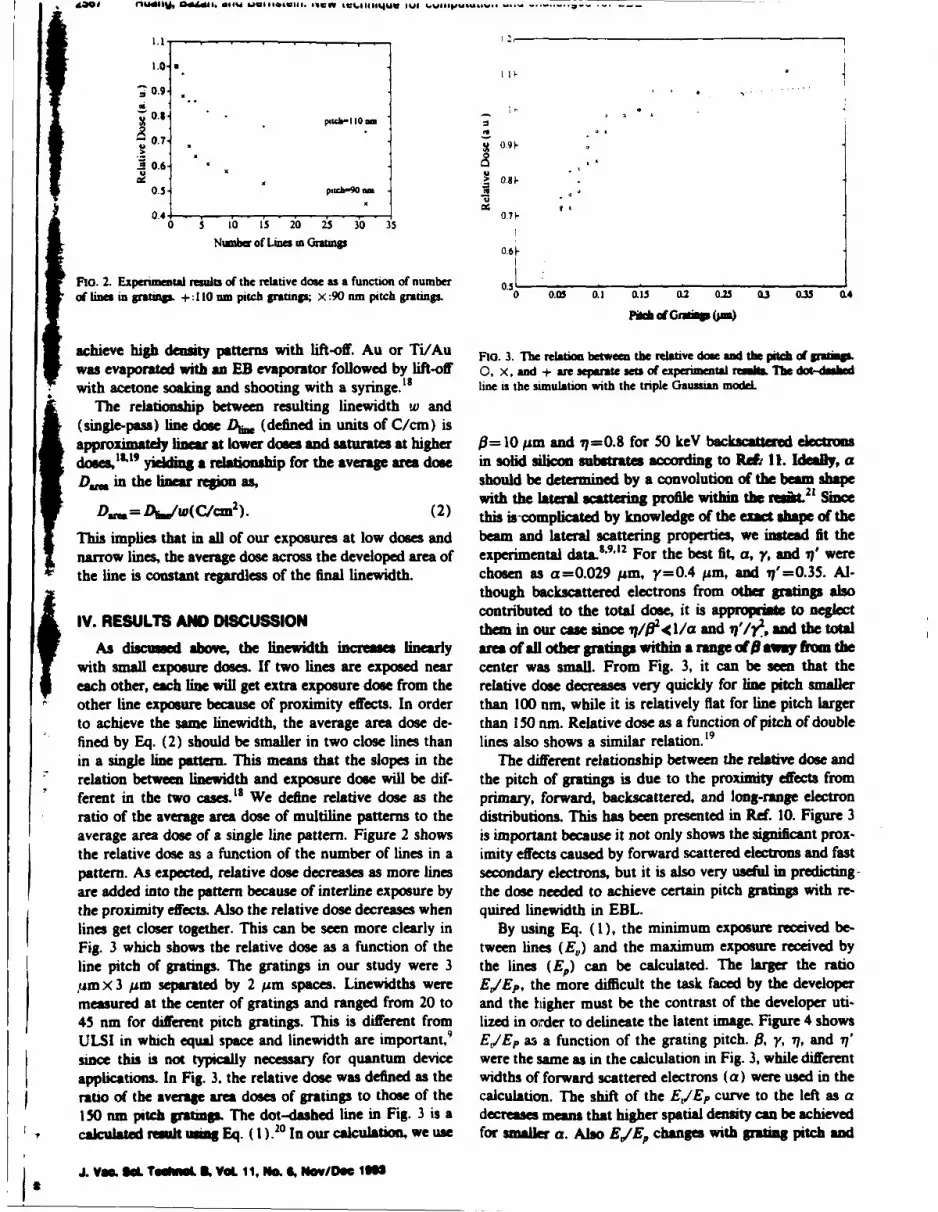
i • i .t I1udWIJ Od1• di. ,.d UU,, u l* -191,,. * w .•.ili*.114U lug , Ul 4. ... .
1.0.
S0.9.
" 0.6
0.5 p.W.-9o am ONT u *,
0.4 0.7-0 S 10 1S 0 2 30o 35
Numba of Lines in ratinp .6
Mio. 2. Ex m raults of the relative dos as a function of number 0.5oflines in grating. +:I10 am pitch $ratings X:90 am pitch gratinp. 0 0.0 0.1 0.1W 0.2 0M 1 0.3 0.35 04
achieve high density patterns with lift-off. Au or Ti/Au FIG. 3. 7"he relatio between tde relative dose and the Pith of grtnS.Uwas evaporated with an EB evaporator followed by lift-off O, x, and + are separate sew of experimental reihLt The dot-dmtewith acetone soaking and shooting with a syringe. 8 line is the simulation with the triple Gaussian model
Terelationship between resulting linewidth wo and
(single-pass) line dose Dhn (defined in units of C/cm) isapproximately linear at lower doses and saturates at higher =10 m and 7-=0.8 for 50 keV backacattered electrondoesm," 9 yielding a relationship for the average area dose in solid silicon substrates according to Raft 11. Ideally, a
Dag. in the linear region as, should be determined by a convolution of the beam shapeSwith the lateral scattering profile within the remt.2 Since
D~m = D&./w(C/cm2 ). (2) this is-complicated by knowledge of the exact shape of the
This implies that in all of our exposures at low doses and beam and lateral scattering properties, we instead fit thenarrow lines, the average dose across the developed area of experimental data.""9.12 For the best fit, a, y, and 71' were
the line is constant regardless of the final linewidth. chosen as a=0.029 Asm, y=0.4 Am, and qt'=0.35. Al-though backscattered electrons from other gratings also
. Rcontributed to the total dose, it is appropriate to neglectIV. RESULTS AND DISCUSSION tthem in our case since i9/0-0 1/a and W1'/e., and the total
As discused abmve, the linewidth incresm linearly are of all other gratings within a range ofig away fom thewith small exposure doses. If two lines are exposed near center was small. From Fig. 3, it can be sewe that theeach other, each line will get extra exposure dose from the relative dose decreases very quickly for line pitch smallerother line exposure because of proximity effects. In order than 100 nm, while it is relatively flat for line pitch largerto achieve the same linewidth, the average area dose de- than 150 nm. Relative dose as a function of pitch of doublefined by Eq. (2) should be smaller in two close lines than lines also shows a similar relation. 19
in a single line pattern. This means that the slopes in the The different relationship between the relative dose andrelation between linewidth and exposure dose will be dif- the pitch of gratings is due to the proximity effects fromferent in the two casesm18 We define relative dose as the primary, forward, backscattered, and long-range electronratio of the average area dose of multiline patterns to the distributions. This has been presented in Ref. 10. Figure 3average area dose of a single line pattern. Figure 2 shows is important because it not only shows the significant prox-the relative dose as a function of the number of lines in a imity effects caused by forward scattered electrons and fastpattern. As expected, relative dose decreases as more lines secondary electrons, but it is also very useful in predicting-are added into the pattern because of interline exposure by the dose needed to achieve certain pitch gratings with re-the proximity effects. Also the relative dose decreases when quired linewidth in EBL.lines get closer together. This can be seen more clearly in By using Eq. (1), the minimum exposure received be-Fig. 3 which shows the relative dose as a function of the tween lines (E,) and the maximum exposure received byline pitch of gratings. The gratings in our study were 3 the lines (E.) can be calculated. The larger the ratioIm X 3 Am separated by 2 Am spaces. Linewidths were E/Ep, the more difficult the task faced by the developermeasured at the center of gratings and ranged from 20 to and the higher must be the contrast of the developer uti-45 nm for different pitch gratings. This is different from lized in order to delineate the latent image. Figure 4 showsULSI in which equal space and linewidth are important,9 E/Ep as a function of the grating pitch. 0, -, 17, and 71'since this is not typically necessary for quantum device were the same as in the calculation in Fig. 3, while differentapplications. In Fig. 3. the relative dose was defined as the widths of forward scattered electrons (a) were used in theratio of the average area doses of gratings to those of the calculation. The shift of the E/Ep curve to the left as a150 nm pitch gratinmg The dot--dashed line in Fig. 3 is a decreases means that higher spatial density can be achievedcalculated remult using Eq. (1 ).20 In our calculation, we use for smaler a. Also E/EP changes with grating pitch and
J. Vs. S& Tedm, IL VOL 11, No. M, Nov/Dee 1M
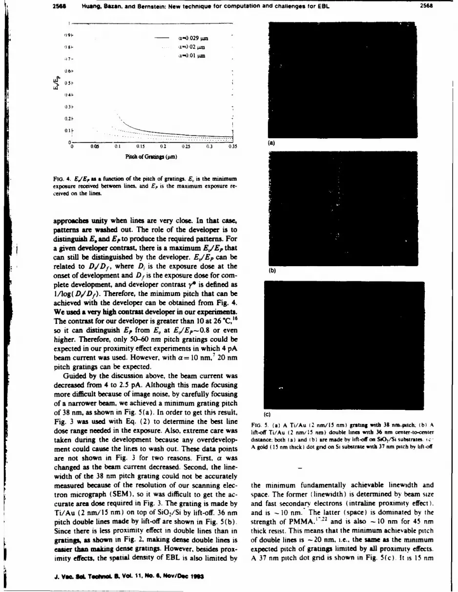
2568 Huang, Bazan, and Bernstein: New technique for computation and challenges for EBL 2568
9 ct-O0.29jiu
'8• • ,=O 02 m
0 6
05"
0 4
03ý
S~~0.I1 -"
0 0.o 0.1 0.15 012 0.25 0. 0.35 (a)
Pitch of GratUp (pm)
FIG. 4. El/Ep as a function of the pitch of gratings. E, is the minimumexposure received between lines, and Ep is the maximum exposure re-ceived on the lines.
approaches unity when lines are very close. In that case,patterns are washed out. The role of the developer is todistinguish E, and Ep to produce the required patterns. Fora given developer contrast, there is a maximum E/Ep thatcan still be distinguished by the developer. E/Ep can berelated to D/Df, where Di is the exposure dose at theonset of development and Df is the exposure dose for com-
plete development, and developer contrast y* is defined asl/log(D./Df). Therefore, the minimum pitch that can beachieved with the developer can be obtained from Fig. 4.We used a very high contrast developer in our experiments.The contrast for our developer is greater than 10 at 26 "C,16
so it can distinguish Ep from E, at E/Ep-0.8 or evenhigher. Therefore, only 50-60 nm pitch gratings could beexpected in our proximity effect experiments in which 4 pAbeam current was used. However, with a= 10 nm,7 20 nmpitch gratings can be expected.
Guided by the discussion above, the beam current wasdecreased from 4 to 2.5 pA. Although this made focusingmore difficult because of image noise, by carefully focusingof a narrower beam, we achieved a minimum grating pitchof 38 nm, as shown in Fig. 5(a). In order to get this result, (c)Fig. 3 was used with Eq. (2) to determine the best line FIG. 5. (a) A Ti/Au (2 nm/iS nm) grating with 38 nm tch, (b) A
dose range needed in the exposure. Also, extreme care was lift-off Ti/Au (2 nm/15 nm) double lines with 36 nm center-to-center
taken during the development because any overdevelop- distance; both (a) and (bi are made by lift-off on SKO,/Si substrates. c ý
ment could cause the lines to wash out. These data points A gold ( 15 nm thick) dot gnd on Si substrate with 37 nm pitch by lift-off
are not shown in Fig. 3 for two reasons. First, a waschanged as the beam current decreased. Second. the line-width of the 38 nm pitch grating could not be accuratelymeasured because of the resolution of our scanning elec- the minimum fundamentally achievable linewidth andtron micrograph (SEM), so it was difficult to get the ac- space. The former (linewidth) is determined by beam sizecurate area dose required in Fig. 3. The grating is made by and fast secondary electrons (intraline proximity effect).Ti/Au (2 nm/15 nm) on top of SiO 2/Si by lift-off. 36 nm and is - 10 nm. The latter (space) is dominated by thepitch double lines made by lift-off are shown in Fig. 5(b). strength of PMMA, 1' 22 and is also - 10 nm for 45 nmSince there is less proximity effect in double lines than in thick resist. This means that the minimum achievable pitchgratings, as shown in Fig. 2. making dense double lines is of double lines is -20 nm. i.e., the same as the minimumeasier than making dense gratings. However, besides prox- expected pitch of gratings limited by all proxirmty effects.
imity effects, the spatial density of EBL is also limited by A 37 nm pitch dot grid is shown in Fig. 5(c). It is 15 nm
J. Va. S& Todw"oL &k Vol 11, No. 6, Nov/Doe 1N,

2569 Huang, Bazan, and Bernstein: New technique for computation and challenges for EDL 2569
thick Au on a Si substrate made by lift-off. This micro- P B. Fischer and S. Y Chou. Appi. Phys. Lett. 62, 2989 (1993).
graph was obtained with a Topcon model ABT-150F field A. G. Rogo and G D. Mahan. Phys. Rev. Lett. 6., 2074 (19921.
emission SEM. Since there is much less proximity effect in C S Lent. P D Tougaw. and W Porod. App). Phys. Lett. 62. 114149•3)
making dot grids, and the strength of PMMA is not as 4c S Leng. P D Tougaw. W Porod. and G H. Bernstem. Nanotech.important in this case, 10 nm diam dots with 15 nm pitch nology 4. 49 ( q93)
dot grids can be expected. D R. Alice and A N Broers. Appl Phys Lett. 57, 2271 (1990)"D. R Alice. C P Umbach, and A N Broers. J Vaic. Sci Technol B
V. SUMMARY AND CONCLUSIONS 9.2838 (1991)"D C Joy. Microeiectron Eng. 1. 103 , l'83)
We discussed a new paradigm in computing called 'R J Bojko and B. J Hughes, J Vac ScL Technol. B. 1909 (1990'quantum cellular automata and related the physical prop- 'S. J Wind, M. G. Rosenlield. G Pepper. W Wý Molten. and P Derties of the quantum structures to the limits of EBL. We Gerber. J. Vac. Sci. Technol. B 7. 1507 (1989); M. G. Rosenfeld. S I
Wind. W W Molzen. and P D Gerber. Microeiacron. Eng. 11. 617investigated proximity effects in order to predict the ulti- (199).mate size of the achievable dot arrays for QCA applica- '.X. Huang. G. H. Bernstein, G. Bazzan. and D. A. Hill, J Vac. Sciti3ns. We investigated properties of dense gratings and dot Technol. A 11, 1739 (1993).arrays with a minimum achieved double line pitch of 36 ((P M. Mankiewich. L. D. Jackel. and R E Howard. J. Vac Sci. Tech-
nm. We predict that dot arrays with a pitch of 15 nm no). B 3. 174 (1985)."",S. A. Rashton and D. P. Kern, J. Vac Sa. TechooL B 5, 135 (1987)should be achievable. Thus, the requirements for the fab- '3 R. C. Frye. J. Vac. Sci. Technol. B 9. 3054 (1991).
rication of dense arrays of dots for applications to quantum 'S. Y Lee. . C Jacob. C M. Chen. J A McMiLln. and N C McDon.cellular automata are predicted to be within the physical aid. J. Vac. Sci. Technol. B 9. 3048 (1991)limits of lift-off technology using PMMA resist and EBL. '5G Bazan and G. H. Bernstein. I Vac. Sc: Technol. A 11. 1745 (1993)
"•G. H. Bernstein, D. A. Hill. and W -P Lu, J. ApI.- Pbyts 71. 4066
ACKNOWLEDGMENTS (1"2)."D. A. Hill. X. Hua..5 G. Bevan and G. H. im J. App& Phys. 72.
The authors thank W. Porod, C. S. Lent, and P. D. 4088 (1992).Tougaw for helpful discussions. This work was supported "S. Mackue and S. P. Beaumont. Solid State Technal. 117 (1985)-
by the National Science Foundation, the National Space "X Huang and G. H Bernstein (unpublishd).'°T. H. P Chan•g, J. Vac. Sci. Technol. 12. 1271 (1975).
Grant College and Fellowship Program, the Air Force Of- 2t H P G h and T van Teco 1r. 1271Dec975.I' S. Creeneich and T. van Duzer, IEEE Trans. Electron Device ED-21ifice of Scientific Research, and the Office of Naval Re- 286 (1974).
search. They also thank Topcon Technologies Inc. for pro- --X. Huang, G. Bazan, D A. Hill. and GC H Berntetn J Electrochernviding field emission SEM micrographs. Soc. 139. 2852 (1992)
j. Ves. Igi. Teaftdi. K VO. 11, o., N6 V/Dec IMS