Embed Size (px)
Citation preview
The following document contains information on Cypress products. The document has the series name, product name, and ordering part numbering with the prefix “MB”. However, Cypress will offer these products to new and existing customers with the series name, product name, and ordering part number with the prefix “CY”. How to Check the Ordering Part Number 1. Go to www.cypress.com/pcn. 2. Enter the keyword (for example, ordering part number) in the SEARCH PCNS field and click
Apply. 3. Click the corresponding title from the search results. 4. Download the Affected Parts List file, which has details of all changes For More Information Please contact your local sales office for additional information about Cypress products and solutions. About Cypress Cypress is the leader in advanced embedded system solutions for the world's most innovative automotive, industrial, smart home appliances, consumer electronics and medical products. Cypress' microcontrollers, analog ICs, wireless and USB-based connectivity solutions and reliable, high-performance memories help engineers design differentiated products and get them to market first. Cypress is committed to providing customers with the best support and development resources on the planet enabling them to disrupt markets by creating new product categories in record time. To learn more, go to www.cypress.com.
www.cypress.com Document No. 002-05317 Rev. *C 1
AN205317
FR, MB91460, FR Clocks
The FR Family MCUs feature a sophisticated clock distribution scheme with the different clock sources such as RC
Clock, Main Clock, PLL Clock, Modulated PLL Clock, and Sub Clock. The core and the peripherals are connected to
different clock trees that can be connected to different clock sources and clock frequencies to allow for a fine-grained
control over the required operation speed and power consumption.
Contents
1 Introduction ............................................................... 1 2 Clock Tree ................................................................ 1
2.1 Overview ...................................................... 1 2.2 RC Clock ...................................................... 2 2.3 Main Clock ...................................................... 2 2.4 PLL Clock ...................................................... 2 2.5 Sub Clock ...................................................... 3 2.6 Clock Modulator ............................................... 3
3 Registers .................................................................. 5 3.1 Clock Source Control Register (CLKR) ............... 5 3.2 Clock Division Setting Register 0 (DIVR0) .......... 5 3.3 Clock Division Setting Register 0 (DIVR1) .......... 5 3.4 Clock Source Configuration Register (CSCFG) .. 6 3.5 Oscillation Control Register (OSCCR) ................ 7 3.6 PLL Control Registers (PLLDIVM) ...................... 7 3.7 PLL Control Registers (PLLDIVN) ....................... 7
3.8 PLL Control Registers (PLLDIVG) ...................... 8 3.9 PLL Control Registers (PLLMULG) ..................... 8 3.10 PLL Control Registers (PLLCTRL) ...................... 8 3.11 Clock Supervisor Control Register (CSVCR) ...... 9 3.12 Clock Modulator Control Register (CMCR) ....... 10 3.13 Clock Modulation Parameter Register (CMPR) 10
4 Using the start.asm ................................................ 11 5 Clock setup sequence ............................................ 13
5.1 Clock Setup Sequence (Example) .................... 14 6 Clock Modulator Configuration ............................... 17 7 Clocks Example ...................................................... 18
7.1 Starting Clock Modulator .................................. 18 7.2 Stopping Clock Modulator ................................. 18
8 Additional Information ............................................. 19 Document History ............................................................ 20
1 Introduction
The FR Family MCUs feature a sophisticated clock distribution scheme with the different clock sources such as RC Clock, Main Clock, PLL Clock, Modulated PLL Clock, and Sub Clock. The core and the peripherals are connected to different clock trees that can be connected to different clock sources and clock frequencies to allow for a fine-grained control over the required operation speed and power consumption.
2 Clock Tree
The FR Family MCUs feature a sophisticated clock distribution that allows for fine-grained control over the used clocks and frequencies. The details are given below.
2.1 Overview
The FR Family can be used with 2 different external clocks: the Main Clock and the Sub Clock and 1 internal (on-chip) clock: the RC Clock. The external clocks may be connected to an oscillator, an oscillation circuit of a crystal and capacitors, or an external clock supply. The internal RC Clock can be configured at 2 MHz or 100 kHz.
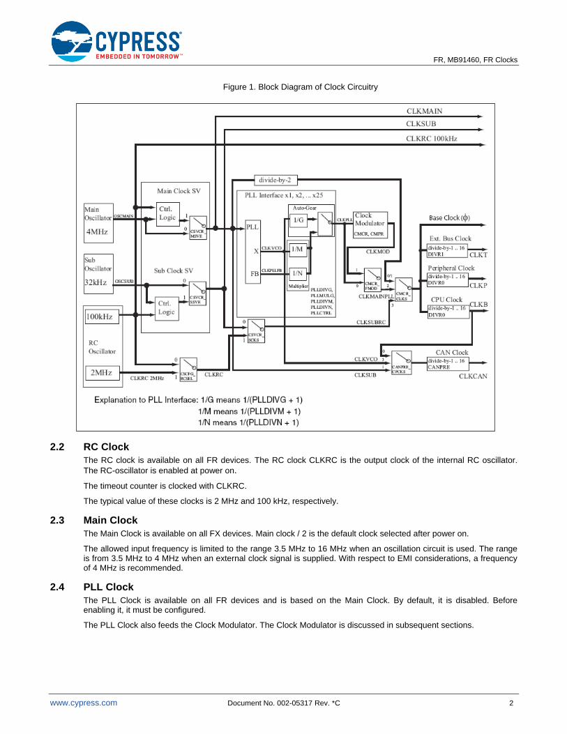
Internally, 4 different clocks are used: the core clock CLKB, the peripheral clock CLKP, External bus clock CLKT and CAN clock CLKCAN. The CLKB provides the clock to the CPU. The CLKCAN provides the clock to the CAN controllers. The CLKP provides the clock for all other peripherals.
Each of these four clocks features a separate prescaler. The following block diagram shows the clock distribution.
FR, MB91460, FR Clocks
www.cypress.com Document No. 002-05317 Rev. *C 2
Figure 1. Block Diagram of Clock Circuitry
2.2 RC Clock
The RC clock is available on all FR devices. The RC clock CLKRC is the output clock of the internal RC oscillator.
The RC-oscillator is enabled at power on.
The timeout counter is clocked with CLKRC.
The typical value of these clocks is 2 MHz and 100 kHz, respectively.
2.3 Main Clock
The Main Clock is available on all FX devices. Main clock / 2 is the default clock selected after power on.
The allowed input frequency is limited to the range 3.5 MHz to 16 MHz when an oscillation circuit is used. The range is from 3.5 MHz to 4 MHz when an external clock signal is supplied. With respect to EMI considerations, a frequency of 4 MHz is recommended.
2.4 PLL Clock
The PLL Clock is available on all FR devices and is based on the Main Clock. By default, it is disabled. Before enabling it, it must be configured.
The PLL Clock also feeds the Clock Modulator. The Clock Modulator is discussed in subsequent sections.
FR, MB91460, FR Clocks
www.cypress.com Document No. 002-05317 Rev. *C 3
2.5 Sub Clock
The Sub Clock is available on all FR dual-clock devices. It can be used as a supplemental clock for low-power applications. By default, it is enabled, but needs to be selected before use.
The allowed input frequency is limited to the range 32 kHz to 100 kHz when an oscillation circuit is used, while the range is extended from 0 Hz to 100 kHz when an external clock signal is supplied. Most time-dependent peripherals offer clock prescalers to allow for full-second intervals when a frequency of 32.768 kHz is provided.
2.6 Clock Modulator
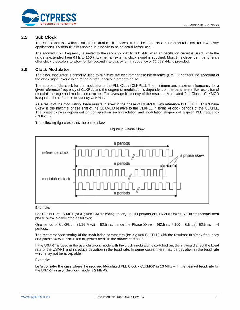
The clock modulator is primarily used to minimize the electromagnetic interference (EMI). It scatters the spectrum of the clock signal over a wide range of frequencies in order to do so.
The source of the clock for the modulator is the PLL Clock (CLKPLL). The minimum and maximum frequency for a given reference frequency of CLKPLL and the degree of modulation is dependent on the parameters like resolution of modulation range and modulation degrees. The average frequency of the resultant Modulated PLL Clock - CLKMOD is equal to the reference frequency CLKPLL.
As a result of the modulation, there results in skew in the phase of CLKMOD with reference to CLKPLL. This ‘Phase Skew’ is the maximal phase shift of the CLKMOD relative to the CLKPLL in terms of clock periods of the CLKPLL. The phase skew is dependent on configuration such resolution and modulation degrees at a given PLL frequency (CLKPLL).
The following figure explains the phase skew:
Figure 2. Phase Skew
Example:
For CLKPLL of 16 MHz (at a given CMPR configuration), if 100 periods of CLKMOD takes 6.5 microseconds then phase skew is calculated as follows:
One period of CLKPLL = (1/16 MHz) = 62.5 ns, hence the Phase Skew = (62.5 ns * 100 – 6.5 µs)/ 62.5 ns = -4 periods.
The recommended setting of the modulation parameters (for a given CLKPLL) with the resultant min/max frequency and phase skew is discussed in greater detail in the hardware manual.
If the USART is used in the asynchronous mode with the clock modulator is switched on, then it would affect the baud rate of the USART and introduce deviation in the baud rate. In some cases, there may be deviation in the baud rate which may not be acceptable.
Example:
Let’s consider the case where the required Modulated PLL Clock - CLKMOD is 16 MHz with the desired baud rate for the USART in asynchronous mode is 2 MBPS.
FR, MB91460, FR Clocks
www.cypress.com Document No. 002-05317 Rev. *C 4
Here the BGRn register needs to be configured with the value of 0x0007. So the deviation in the baud rate as per USART chapter in the hardware manual is 0. But the CLKMOD would also have an impact on this deviation of baud rate.
Lets also consider that the character format is 8E1 that means one USART character contains 11 bits (1 Start bit + 8 Data bits + 1 Even Parity bit + 1 Stop bit).
If the data that needs to be transmitted is 0x00, the parity bit would also be zero and the USART output should remain at low level for period of 10 bits. These 10 bits corresponds to the 80 clock periods (cycles) of CLKMOD.
Let’s also consider that the clock modulator is configured for the resolution of 11 and modulation degree of 1 then the “± phase skew min/max” would be 7.875. This means that the 80 clock periods would be either shortened to 72.125 clock periods or may get lengthened to 87.875 clock period that is the error of up to 1 bit. This may cause parity error or framing error respectively at the receiver.
FR, MB91460, FR Clocks
www.cypress.com Document No. 002-05317 Rev. *C 5
3 Registers
The configuration of the Clock Tree is controlled by the following Registers:
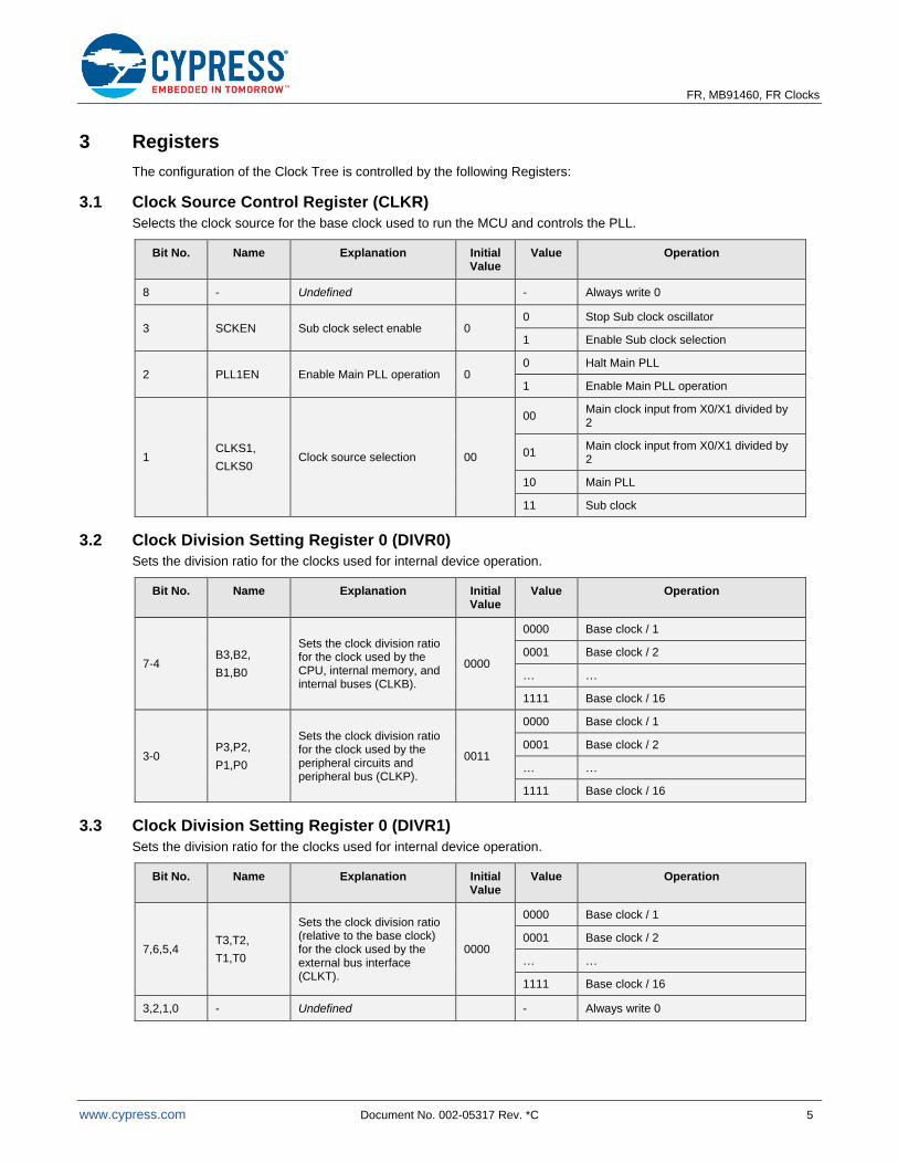
3.1 Clock Source Control Register (CLKR)
Selects the clock source for the base clock used to run the MCU and controls the PLL.
Bit No. Name Explanation Initial Value
Value Operation
8 - Undefined - Always write 0
3 SCKEN Sub clock select enable 0 0 Stop Sub clock oscillator
1 Enable Sub clock selection
2 PLL1EN Enable Main PLL operation 0 0 Halt Main PLL
1 Enable Main PLL operation
1 CLKS1,
CLKS0 Clock source selection 00
00 Main clock input from X0/X1 divided by 2
01 Main clock input from X0/X1 divided by 2
10 Main PLL
11 Sub clock
3.2 Clock Division Setting Register 0 (DIVR0)
Sets the division ratio for the clocks used for internal device operation.
Bit No. Name Explanation Initial Value
Value Operation
7-4 B3,B2,
B1,B0
Sets the clock division ratio for the clock used by the CPU, internal memory, and internal buses (CLKB).
0000
0000 Base clock / 1
0001 Base clock / 2
… …
1111 Base clock / 16
3-0 P3,P2,
P1,P0
Sets the clock division ratio for the clock used by the peripheral circuits and peripheral bus (CLKP).
0011
0000 Base clock / 1
0001 Base clock / 2
… …
1111 Base clock / 16
3.3 Clock Division Setting Register 0 (DIVR1)
Sets the division ratio for the clocks used for internal device operation.
Bit No. Name Explanation Initial Value
Value Operation
7,6,5,4 T3,T2,
T1,T0
Sets the clock division ratio (relative to the base clock) for the clock used by the external bus interface (CLKT).
0000
0000 Base clock / 1
0001 Base clock / 2
… …
1111 Base clock / 16
3,2,1,0 - Undefined - Always write 0
FR, MB91460, FR Clocks
www.cypress.com Document No. 002-05317 Rev. *C 6
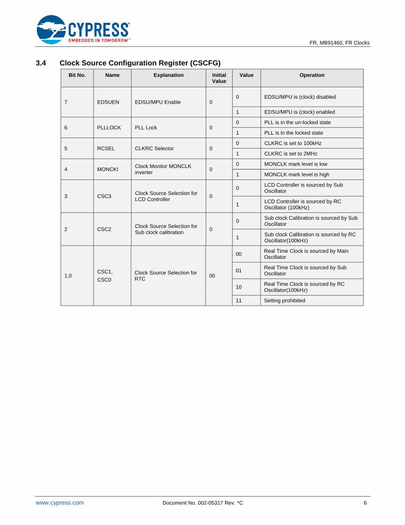
3.4 Clock Source Configuration Register (CSCFG)
Bit No. Name Explanation Initial Value
Value Operation
7 EDSUEN EDSU/MPU Enable 0 0 EDSU/MPU is (clock) disabled
1 EDSU/MPU is (clock) enabled
6 PLLLOCK PLL Lock 0 0 PLL is in the un-locked state
1 PLL is in the locked state
5 RCSEL CLKRC Selector 0 0 CLKRC is set to 100kHz
1 CLKRC is set to 2MHz
4 MONCKI Clock Monitor MONCLK inverter
0 0 MONCLK mark level is low
1 MONCLK mark level is high
3 CSC3 Clock Source Selection for LCD Controller
0
0 LCD Controller is sourced by Sub Oscillator
1 LCD Controller is sourced by RC Oscillator (100kHz)
2 CSC2 Clock Source Selection for Sub clock calibration
0
0 Sub clock Calibration is sourced by Sub Oscillator
1 Sub clock Calibration is sourced by RC Oscillator(100kHz)
1,0 CSC1,
CSC0
Clock Source Selection for RTC
00
00 Real Time Clock is sourced by Main Oscillator
01 Real Time Clock is sourced by Sub Oscillator
10 Real Time Clock is sourced by RC Oscillator(100kHz)
11 Setting prohibited
FR, MB91460, FR Clocks
www.cypress.com Document No. 002-05317 Rev. *C 7
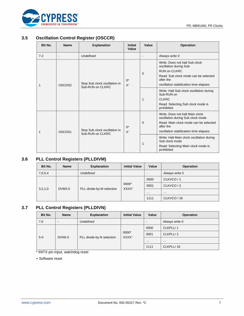
3.5 Oscillation Control Register (OSCCR)
Bit No. Name Explanation Initial Value
Value Operation
7-2 - Undefined - Always write 0
1 OSCDS2 Stop Sub clock oscillation in Sub-RUN on CLKRC
0*
X+
0
Write: Does not halt Sub clock oscillation during Sub-
RUN on CLKRC
Read: Sub clock mode can be selected after the
oscillation stabilization time elapses
1
Write: Halt Sub clock oscillation during Sub-RUN on
CLKRC
Read: Selecting Sub clock mode is prohibited
1 OSCDS1 Stop Sub clock oscillation in Sub-RUN on CLKRC
0*
X+
0
Write: Does not halt Main clock oscillation during Sub clock mode
Read: Main clock mode can be selected after the
oscillation stabilization time elapses
1
Write: Halt Main clock oscillation during Sub clock mode
Read: Selecting Main clock mode is prohibited
3.6 PLL Control Registers (PLLDIVM)
Bit No. Name Explanation Initial Value Value Operation
7,6,5,4 - Undefined - Always write 0
3,2,1,0 DVM3-0 PLL divide-by-M selection
0000*
XXXX+
0000 CLKVCO / 1
0001 CLKVCO / 2
… …
1111 CLKVCO / 16
3.7 PLL Control Registers (PLLDIVN)
Bit No. Name Explanation Initial Value Value Operation
7,6 - Undefined - Always write 0
5-0 DVN5-0 PLL divide-by-N selection
0000*
XXXX+
0000 CLKPLL/ 1
0001 CLKPLL/ 2
… …
1111 CLKPLL/ 16
* INITX pin input, watchdog reset
+ Software reset
FR, MB91460, FR Clocks
www.cypress.com Document No. 002-05317 Rev. *C 8
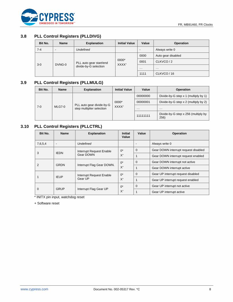
3.8 PLL Control Registers (PLLDIVG)
Bit No. Name Explanation Initial Value Value Operation
7-4 - Undefined - Always write 0
3-0 DVNG-0 PLL auto gear start/end divide-by-G selection
0000*
XXXX+
0000 Auto gear disabled
0001 CLKVCO / 2
… …
1111 CLKVCO / 16
3.9 PLL Control Registers (PLLMULG)
Bit No. Name Explanation Initial Value Value Operation
7-0 MLG7-0 PLL auto gear divide-by-G step multiplier selection
0000*
XXXX+
00000000 Divide-by-G step x 1 (multiply by 1)
00000001 Divide-by-G step x 2 (multiply by 2)
… …
11111111 Divide-by-G step x 256 (multiply by 256)
3.10 PLL Control Registers (PLLCTRL)
Bit No. Name Explanation Initial Value
Value Operation
7,6,5,4 - Undefined - Always write 0
3 IEDN Interrupt Request Enable Gear DOWN
0*
X+
0 Gear DOWN interrupt request disabled
1 Gear DOWN interrupt request enabled
2 GRDN Interrupt Flag Gear DOWN. 0*
X+
0 Gear DOWN interrupt not active
1 Gear DOWN interrupt active
1 IEUP Interrupt Request Enable Gear UP
0*
X+
0 Gear UP interrupt request disabled
1 Gear UP interrupt request enabled
0 GRUP Interrupt Flag Gear UP 0*
X+
0 Gear UP interrupt not active
1 Gear UP interrupt active
* INITX pin input, watchdog reset
+ Software reset
FR, MB91460, FR Clocks
www.cypress.com Document No. 002-05317 Rev. *C 9
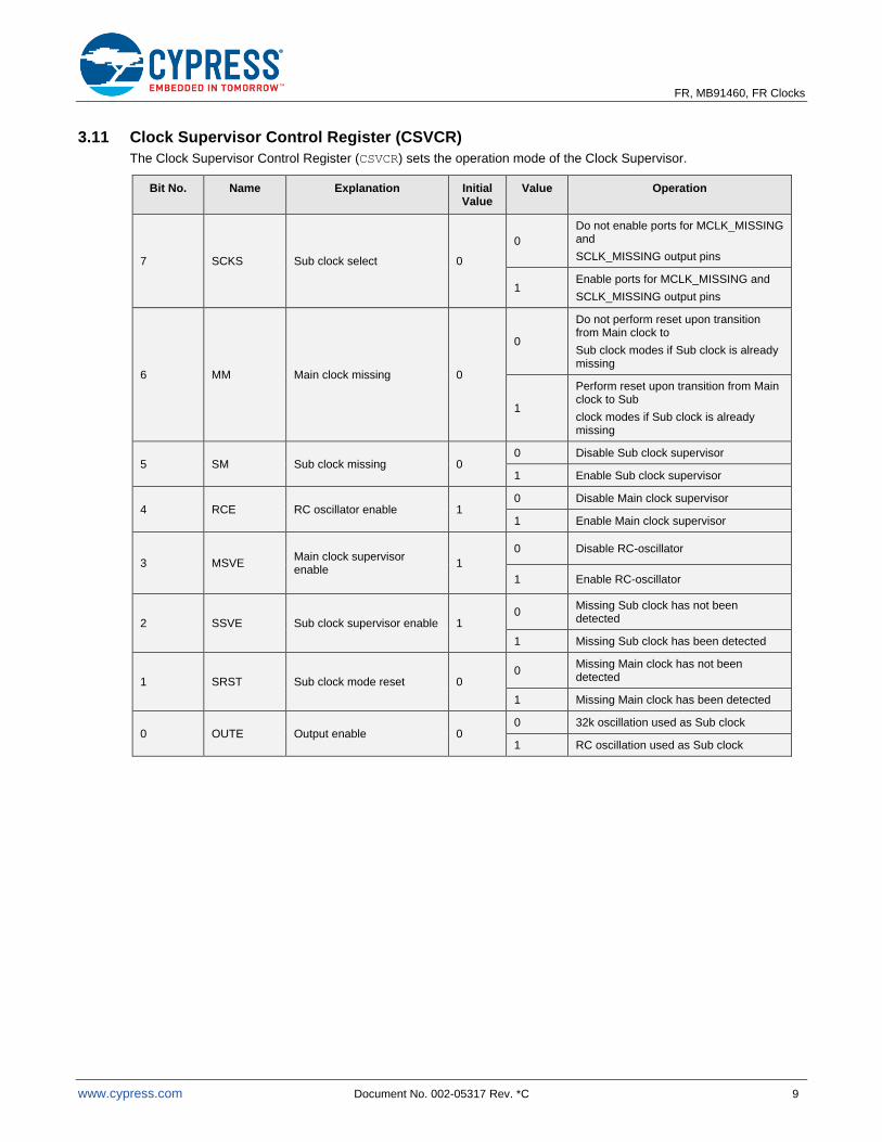
3.11 Clock Supervisor Control Register (CSVCR)
The Clock Supervisor Control Register (CSVCR) sets the operation mode of the Clock Supervisor.
Bit No. Name Explanation Initial Value
Value Operation
7 SCKS Sub clock select 0
0
Do not enable ports for MCLK_MISSING and
SCLK_MISSING output pins
1 Enable ports for MCLK_MISSING and
SCLK_MISSING output pins
6 MM Main clock missing 0
0
Do not perform reset upon transition from Main clock to
Sub clock modes if Sub clock is already missing
1
Perform reset upon transition from Main clock to Sub
clock modes if Sub clock is already missing
5 SM Sub clock missing 0 0 Disable Sub clock supervisor
1 Enable Sub clock supervisor
4 RCE RC oscillator enable 1 0 Disable Main clock supervisor
1 Enable Main clock supervisor
3 MSVE Main clock supervisor enable
1
0 Disable RC-oscillator
1 Enable RC-oscillator
2 SSVE Sub clock supervisor enable 1 0
Missing Sub clock has not been detected
1 Missing Sub clock has been detected
1 SRST Sub clock mode reset 0 0
Missing Main clock has not been detected
1 Missing Main clock has been detected
0 OUTE Output enable 0 0 32k oscillation used as Sub clock
1 RC oscillation used as Sub clock
FR, MB91460, FR Clocks
www.cypress.com Document No. 002-05317 Rev. *C 10
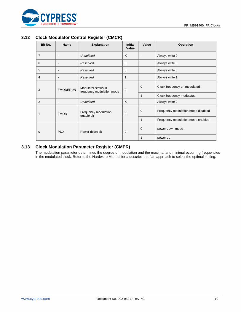
3.12 Clock Modulator Control Register (CMCR)
Bit No. Name Explanation Initial Value
Value Operation
7 - Undefined X - Always write 0
6 - Reserved 0 Always write 0
5 - Reserved 0 Always write 0
4 - Reserved 1 Always write 1
3 FMODERUN Modulator status in frequency modulation mode
0 0 Clock frequency un modulated
1 Clock frequency modulated
2 - Undefined X - Always write 0
1 FMOD Frequency modulation enable bit
0 0 Frequency modulation mode disabled
1 Frequency modulation mode enabled
0 PDX Power down bit 0 0 power down mode
1 power up
3.13 Clock Modulation Parameter Register (CMPR)
The modulation parameter determines the degree of modulation and the maximal and minimal occurring frequencies in the modulated clock. Refer to the Hardware Manual for a description of an approach to select the optimal setting.
FR, MB91460, FR Clocks
www.cypress.com Document No. 002-05317 Rev. *C 11
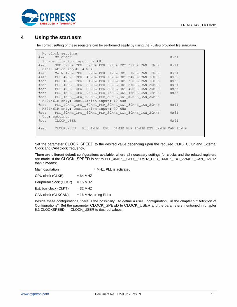
4 Using the start.asm
The correct setting of these registers can be performed easily by using the Fujitsu provided file start.asm.
Set the parameter CLOCK_SPEED to the desired value depending upon the required CLKB, CLKP and External
Clock and CAN clock frequency.
There are different default configurations available, where all necessary settings for clocks and the related registers
are made. If the CLOCK_SPEED is set to PLL_4MHZ__CPU__64MHZ_PER_16MHZ_EXT_32MHZ_CAN_16MHZ
than it means:
Main oscillation = 4 MHz, PLL is activated
CPU clock (CLKB) = 64 MHZ
Peripheral clock (CLKP) = 16 MHZ
Ext. bus clock (CLKT) = 32 MHZ
CAN clock (CLKCAN) = 16 MHz, using PLLx
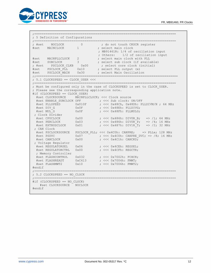
Beside these configurations, there is the possibility to define a user configuration in the chapter 5 "Definition of
Configurations". Set the parameter CLOCK_SPEED to CLOCK_USER and the parameters mentioned in chapter
5.1 CLOCKSPEED == CLOCK_USER to desired values.
; No clock settings
#set NO_CLOCK 0x01
; Sub-oscillation input: 32 kHz
#set SUB_32KHZ_CPU__32KHZ_PER_32KHZ_EXT_32KHZ_CAN__2MHZ 0x11
; Oscillation input: 4 MHz
#set MAIN_4MHZ_CPU___2MHZ_PER__1MHZ_EXT__1MHZ_CAN__2MHZ 0x21
#set PLL_4MHZ__CPU__48MHZ_PER_16MHZ_EXT_24MHZ_CAN_16MHZ 0x22
#set PLL_4MHZ__CPU__64MHZ_PER_16MHZ_EXT_32MHZ_CAN_16MHZ 0x23
#set PLL_4MHZ__CPU__80MHZ_PER_20MHZ_EXT_27MHZ_CAN_20MHZ 0x24
#set PLL_4MHZ__CPU__80MHZ_PER_20MHZ_EXT_40MHZ_CAN_20MHZ 0x25
#set PLL_4MHZ__CPU__96MHZ_PER_16MHZ_EXT_48MHZ_CAN_16MHZ 0x26
#set PLL_4MHZ__CPU_100MHZ_PER_20MHZ_EXT_50MHZ_CAN_20MHZ
; MB91461R only: Oscillation input: 10 MHz
#set PLL_10MHZ_CPU__60MHZ_PER_20MHZ_EXT_30MHZ_CAN_20MHZ 0x41
; MB91461R only: Oscillation input: 20 MHz
#set PLL_20MHZ_CPU__60MHZ_PER_20MHZ_EXT_30MHZ_CAN_20MHZ 0x51
; User settings
#set CLOCK_USER 0x61
;
#set CLOCKSPEED PLL_4MHZ__CPU__64MHZ_PER_16MHZ_EXT_32MHZ_CAN_16MHZ
FR, MB91460, FR Clocks
www.cypress.com Document No. 002-05317 Rev. *C 12
;============================================================================
; 5 Definition of Configurations
;============================================================================
; #set NOCLOCK 0 ; do not touch CKSCR register
#set MAINCLOCK 1 ; select main clock
; MB91461R: 1/4 of oscillation input
; Others: 1/2 of oscillation input
#set MAINPLLCLOCK 2 ; select main clock with PLL
#set SUBCLOCK 3 ; select sub clock (if available)
; #set PSCLOCK_CLKB 0x00 ; select core clock (initial)
#set PSCLOCK_PLL 0x10 ; select PLL output (x)
#set PSCLOCK_MAIN 0x30 ; select Main Oscillation
;;============================================================================
; 5.1 CLOCKSPEED == CLOCK_USER <<<
;============================================================================
; Must be configured only in the case of CLOCKSPEED is set to CLOCK_USER.
; Please see the corresponding application note.
#if (CLOCKSPEED == CLOCK_USER)
#set CLOCKSOURCE MAINPLLCLOCK; <<< Clock source
#set ENABLE_SUBCLOCK OFF ; <<< Sub clock: ON/OFF
#set PLLSPEED 0x010F ; <<< 0x48Ch, 0x48Dh: PLLDIVM/N ; 64 MHz
#set DIV_G 0x0F ; <<< 0x48Eh: PLLDIVG;
#set MUL_G 0x0F ; <<< 0x48Fh: PLLMULG;
; Clock Divider
#set CPUCLOCK 0x00 ; <<< 0x486h: DIV0R_B; => /1; 64 MHz
#set PERCLOCK 0x03 ; <<< 0x486h: DIV0R_P; => /4; 16 MHz
#set EXTBUSCLOCK 0x01 ; <<< 0x487h: DIV1R_T; => /2; 32 MHz
; CAN Clock
#set PSCLOCKSOURCE PSCLOCK_PLL; <<< 0x4C0h: CANPRE; => PLLx; 128 MHz
#set PSDVC 0x07 ; <<< 0x4C0h: CANPRE_DVC; => /8; 16 MHz
#set CANCLOCK 0x00 ; <<< 0x4C1h: CANCKD;
; Voltage Regulator
#set REGULATORSEL 0x06 ; <<< 0x4CEh: REGSEL;
#set REGULATORCTRL 0x00 ; <<< 0x4CFh: REGCTR;
; Memory Controller
#set FLASHCONTROL 0x032 ; <<< 0x7002h: FCHCR;
#set FLASHREADT 0xC413 ; <<< 0x7004h: FMWT;
#set FLASHMWT2 0x10 ; <<< 0x7006h: FMWT2;
#endif
;============================================================================
; 5.2 CLOCKSPEED == NO_CLOCK
;============================================================================
#if (CLOCKSPEED == NO_CLOCK)
#set CLOCKSOURCE NOCLOCK
#endif
FR, MB91460, FR Clocks
www.cypress.com Document No. 002-05317 Rev. *C 13
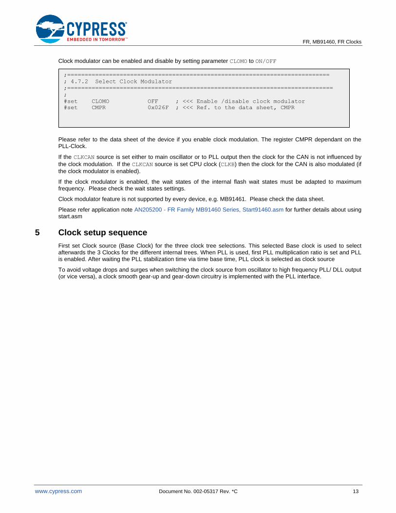
Clock modulator can be enabled and disable by setting parameter CLOMO to ON/OFF
Please refer to the data sheet of the device if you enable clock modulation. The register CMPR dependant on the PLL-Clock.
If the CLKCAN source is set either to main oscillator or to PLL output then the clock for the CAN is not influenced by
the clock modulation. If the CLKCAN source is set CPU clock (CLKB) then the clock for the CAN is also modulated (if
the clock modulator is enabled).
If the clock modulator is enabled, the wait states of the internal flash wait states must be adapted to maximum frequency. Please check the wait states settings.
Clock modulator feature is not supported by every device, e.g. MB91461. Please check the data sheet.
Please refer application note AN205200 - FR Family MB91460 Series, Start91460.asm for further details about using start.asm
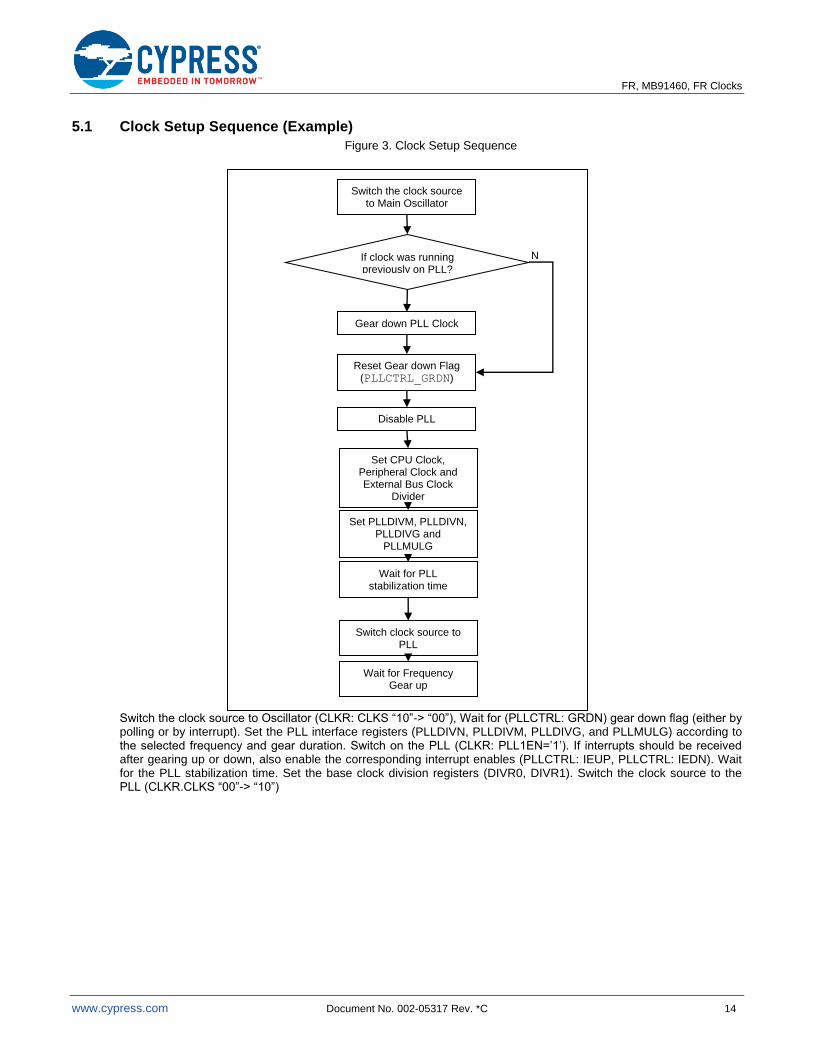
5 Clock setup sequence
First set Clock source (Base Clock) for the three clock tree selections. This selected Base clock is used to select afterwards the 3 Clocks for the different internal trees. When PLL is used, first PLL multiplication ratio is set and PLL is enabled. After waiting the PLL stabilization time via time base time, PLL clock is selected as clock source
To avoid voltage drops and surges when switching the clock source from oscillator to high frequency PLL/ DLL output (or vice versa), a clock smooth gear-up and gear-down circuitry is implemented with the PLL interface.
;===========================================================================
; 4.7.2 Select Clock Modulator
;============================================================================
;
#set CLOMO OFF ; <<< Enable /disable clock modulator
#set CMPR 0x026F ; <<< Ref. to the data sheet, CMPR
FR, MB91460, FR Clocks
www.cypress.com Document No. 002-05317 Rev. *C 14
5.1 Clock Setup Sequence (Example)
Figure 3. Clock Setup Sequence
Switch the clock source to Oscillator (CLKR: CLKS “10”-> “00”), Wait for (PLLCTRL: GRDN) gear down flag (either by polling or by interrupt). Set the PLL interface registers (PLLDIVN, PLLDIVM, PLLDIVG, and PLLMULG) according to the selected frequency and gear duration. Switch on the PLL (CLKR: PLL1EN=’1’). If interrupts should be received after gearing up or down, also enable the corresponding interrupt enables (PLLCTRL: IEUP, PLLCTRL: IEDN). Wait for the PLL stabilization time. Set the base clock division registers (DIVR0, DIVR1). Switch the clock source to the PLL (CLKR.CLKS “00”-> “10”)
NO
Switch the clock source to Main Oscillator
If clock was running previously on PLL?
Gear down PLL Clock
Reset Gear down Flag (PLLCTRL_GRDN)
Disable PLL
Set CPU Clock, Peripheral Clock and External Bus Clock
Divider
Set PLLDIVM, PLLDIVN, PLLDIVG and
PLLMULG
Wait for PLL stabilization time
Switch clock source to PLL
Wait for Frequency Gear up
FR, MB91460, FR Clocks
www.cypress.com Document No. 002-05317 Rev. *C 15
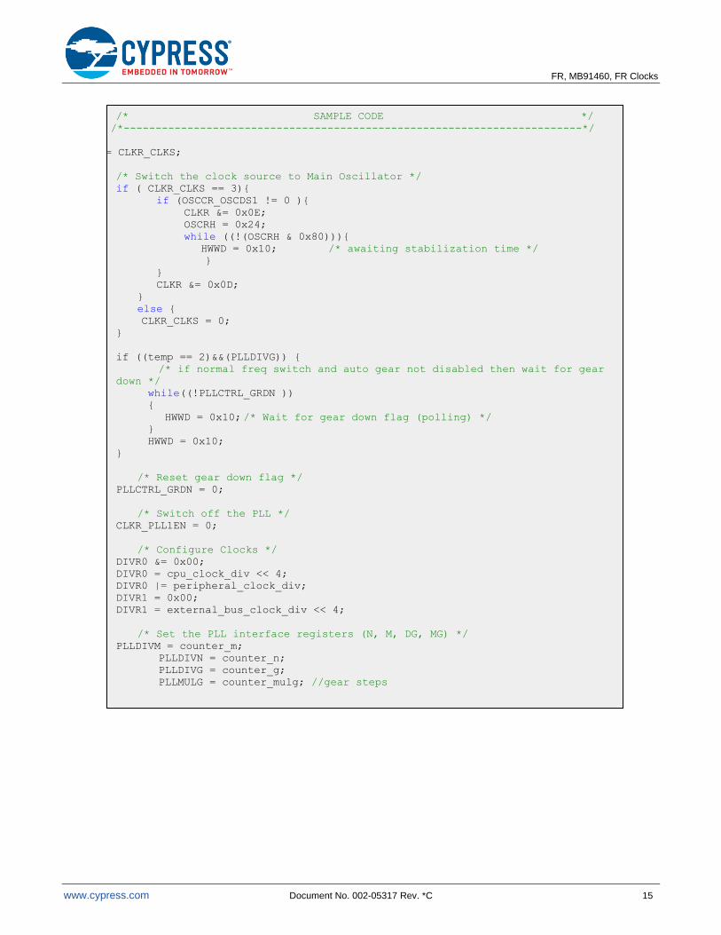
/* SAMPLE CODE */
/*------------------------------------------------------------------------*/
temp = CLKR_CLKS;
/* Switch the clock source to Main Oscillator */
if ( CLKR_CLKS == 3){
if (OSCCR_OSCDS1 != 0 ){
CLKR &= 0x0E;
OSCRH = 0x24;
while ((!(OSCRH & 0x80))){
HWWD = 0x10; /* awaiting stabilization time */
}
}
CLKR &= 0x0D;
}
else {
CLKR_CLKS = 0;
}
if ((temp == 2)&&(PLLDIVG)) {
/* if normal freq switch and auto gear not disabled then wait for gear
down */
while((!PLLCTRL_GRDN ))
{
HWWD = 0x10; /* Wait for gear down flag (polling) */
}
HWWD = 0x10;
}
/* Reset gear down flag */
PLLCTRL_GRDN = 0;
/* Switch off the PLL */
CLKR_PLL1EN = 0;
/* Configure Clocks */
DIVR0 &= 0x00;
DIVR0 = cpu_clock_div << 4;
DIVR0 |= peripheral_clock_div;
DIVR1 = 0x00;
DIVR1 = external_bus_clock_div << 4;
/* Set the PLL interface registers (N, M, DG, MG) */
PLLDIVM = counter_m;
PLLDIVN = counter_n;
PLLDIVG = counter_g;
PLLMULG = counter_mulg; //gear steps
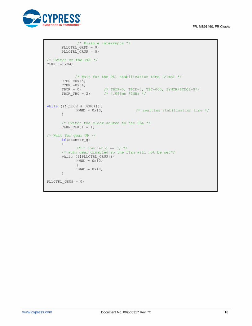
FR, MB91460, FR Clocks
www.cypress.com Document No. 002-05317 Rev. *C 16
/* Disable interrupts */
PLLCTRL_GRDN = 0;
PLLCTRL_GRUP = 0;
/* Switch on the PLL */
CLKR |=0x04;
/* Wait for the PLL stabilization time (>1ms) */
CTBR =0xA5;
CTBR =0x5A;
TBCR = 0; /* TBIF=0, TBIE=0, TBC=000, SYNCR/SYNCS=0*/
TBCR_TBC = 2; /* 4.096ms @2MHz */
while ((!(TBCR & 0x80))){
HWWD = 0x10; /* awaiting stabilisation time */
}
/* Switch the clock source to the PLL */
CLKR_CLKS1 = 1;
/* Wait for gear UP */
if(counter_g)
{
/*if counter_g == 0; */
/* auto gear disabled so the flag will not be set*/
while ((!PLLCTRL_GRUP)){
HWWD = 0x10;
}
HWWD = 0x10;
}
PLLCTRL_GRUP = 0;
FR, MB91460, FR Clocks
www.cypress.com Document No. 002-05317 Rev. *C 17
6 Clock Modulator Configuration
The Clock Modulator has the start up time of 6 μs after it is powered on (using the PDX bit of Clock Modulation
Control Register (CMCR) register). The following are the prerequisites to enable the clock modulator (using the MODEN
bit of CMCR register):
▪ The PLL lock time is elapsed and it is stabilized (i.e. PCM bit of CKMR register is set)
▪ Clock Modulator is powered up and the start up time is elapsed.
▪ The Clock Modulator Parameter Register (CMPR) register is configured with the appropriate value.
The MODRUN bit of the CMCR register reflects the status of modulated clock. If it is 1 then the CLKMOD can be used as
a clock resource for CLKS1.
The CMPR register contains modulation parameter which determines the degree of modulation and the maximal and
minimal occurring frequencies in the modulated clock. Please refer the hardware manual for the correspondence between PLL frequency and possible modulation parameters.
In order to power down the clock modulator its needs to be disabled (using the MODEN bit of CMCR register). After
that, once the MODRUN bit gets cleared to zero, the clock modulator can be powered down.
FR, MB91460, FR Clocks
www.cypress.com Document No. 002-05317 Rev. *C 18
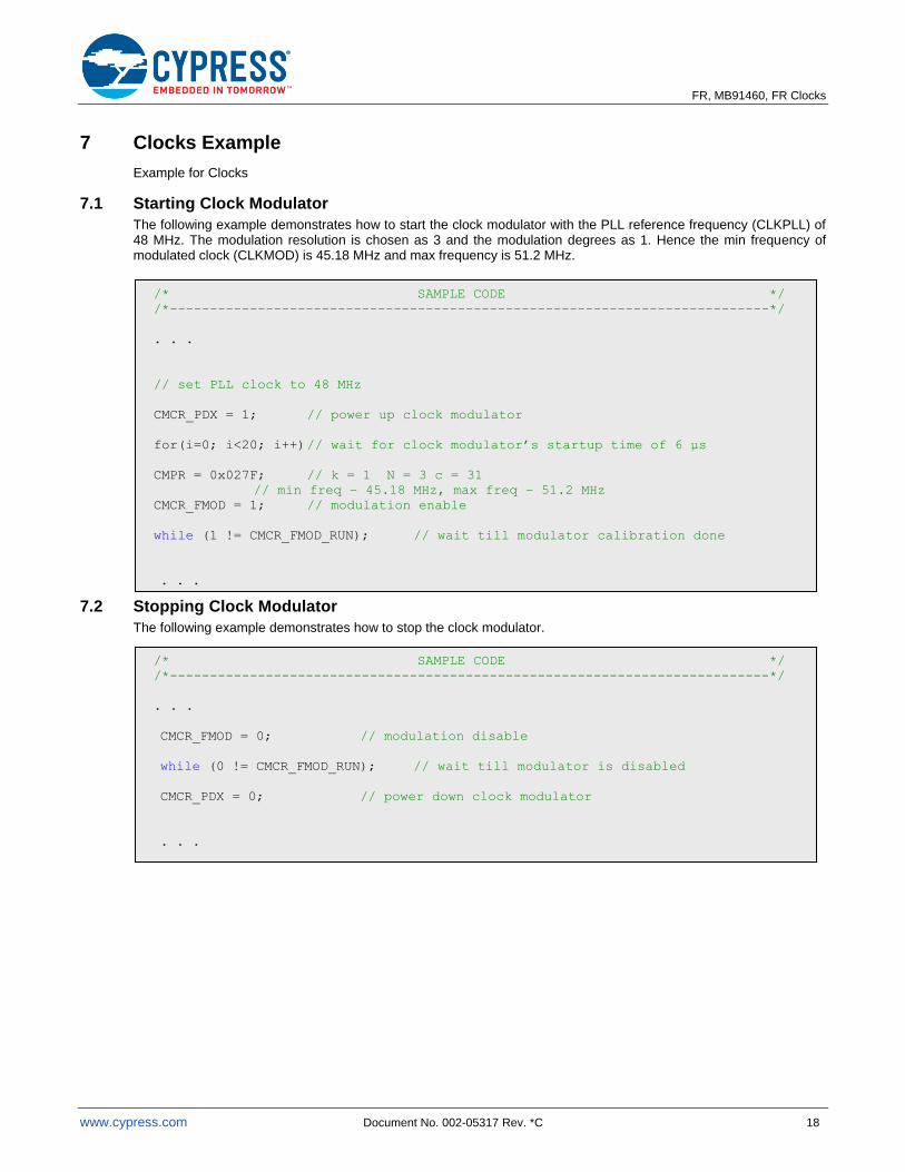
7 Clocks Example
Example for Clocks
7.1 Starting Clock Modulator
The following example demonstrates how to start the clock modulator with the PLL reference frequency (CLKPLL) of 48 MHz. The modulation resolution is chosen as 3 and the modulation degrees as 1. Hence the min frequency of modulated clock (CLKMOD) is 45.18 MHz and max frequency is 51.2 MHz.
7.2 Stopping Clock Modulator
The following example demonstrates how to stop the clock modulator.
/* SAMPLE CODE */
/*---------------------------------------------------------------------------*/
. . .
// set PLL clock to 48 MHz
CMCR_PDX = 1; // power up clock modulator
for(i=0; i<20; i++) // wait for clock modulator’s startup time of 6 μs
CMPR = 0x027F; // k = 1 N = 3 c = 31
// min freq – 45.18 MHz, max freq – 51.2 MHz
CMCR_FMOD = 1; // modulation enable
while (1 != CMCR_FMOD_RUN); // wait till modulator calibration done
. . .
/* SAMPLE CODE */
/*---------------------------------------------------------------------------*/
. . .
CMCR_FMOD = 0; // modulation disable
while (0 != CMCR_FMOD_RUN); // wait till modulator is disabled
CMCR_PDX = 0; // power down clock modulator
. . .
FR, MB91460, FR Clocks
www.cypress.com Document No. 002-05317 Rev. *C 19
8 Additional Information
Information about Cypress Microcontrollers can be found on the following Internet page:
http://www.cypress.com/cypress-microcontrollers
The software examples related to this application note is:
91460_Clock_Modulator
91460_Clock_Setting
It can be found on the following Internet page:
http://www.cypress.com/cypress-mcu-product-softwareexamples
FR, MB91460, FR Clocks
www.cypress.com Document No. 002-05317 Rev. *C 20
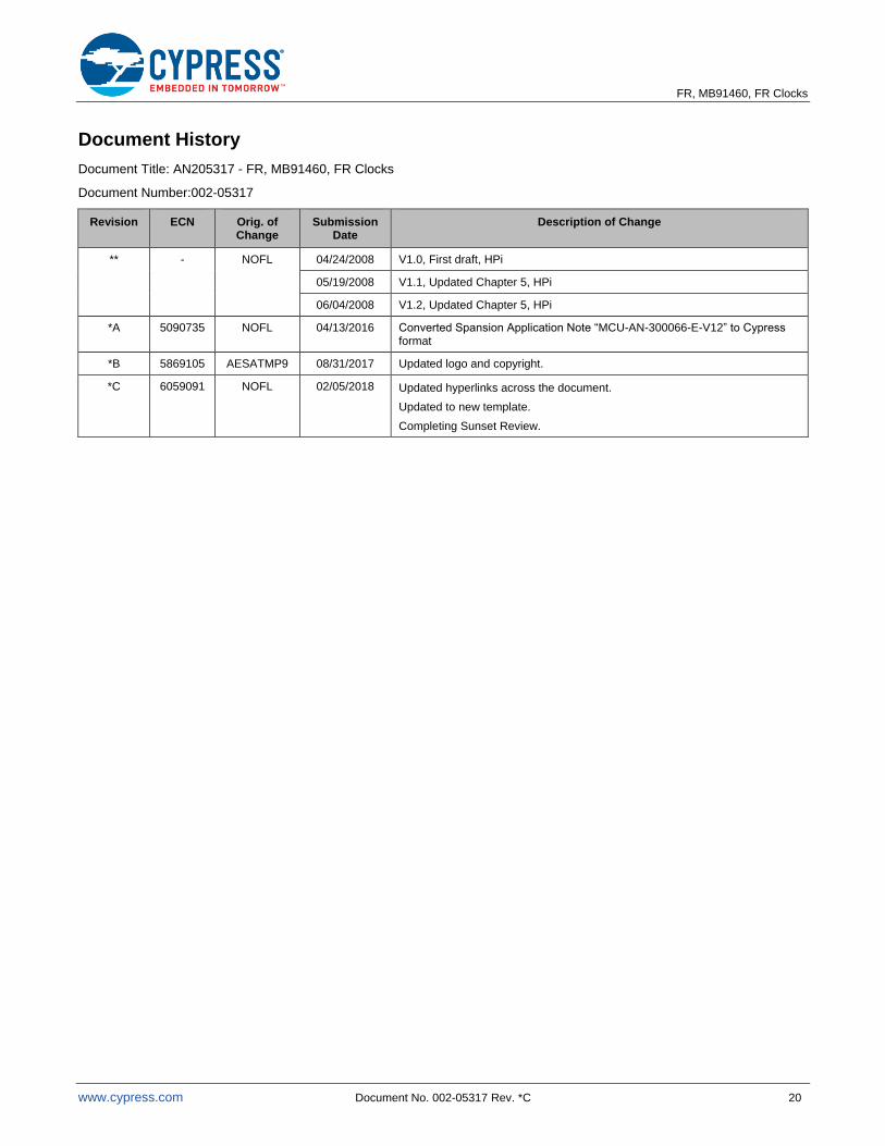
Document History
Document Title: AN205317 - FR, MB91460, FR Clocks
Document Number:002-05317
Revision ECN Orig. of Change
Submission Date
Description of Change
** - NOFL 04/24/2008 V1.0, First draft, HPi
05/19/2008 V1.1, Updated Chapter 5, HPi
06/04/2008 V1.2, Updated Chapter 5, HPi
*A 5090735 NOFL 04/13/2016 Converted Spansion Application Note “MCU-AN-300066-E-V12” to Cypress format
*B 5869105 AESATMP9 08/31/2017 Updated logo and copyright.
*C 6059091 NOFL 02/05/2018 Updated hyperlinks across the document.
Updated to new template.
Completing Sunset Review.
FR, MB91460, FR Clocks
www.cypress.com Document No. 002-05317 Rev. *C 21
Worldwide Sales and Design Support
Cypress maintains a worldwide network of offices, solution centers, manufacturer’s representatives, and distributors. To find the office closest to you, visit us at Cypress Locations.
Products
ARM® Cortex® Microcontrollers cypress.com/arm
Automotive cypress.com/automotive
Clocks & Buffers cypress.com/clocks
Interface cypress.com/interface
Internet of Things cypress.com/iot
Memory cypress.com/memory
Microcontrollers cypress.com/mcu
PSoC cypress.com/psoc
Power Management ICs cypress.com/pmic
Touch Sensing cypress.com/touch
USB Controllers cypress.com/usb
Wireless Connectivity cypress.com/wireless
PSoC® Solutions
PSoC 1 | PSoC 3 | PSoC 4 | PSoC 5LP | PSoC 6 MCU
Cypress Developer Community
Community | Projects | Videos | Blogs | Training | Components
Technical Support
cypress.com/support
Cypress Semiconductor 198 Champion Court San Jose, CA 95134-1709
© Cypress Semiconductor Corporation, 2008-2018. This document is the property of Cypress Semiconductor Corporation and its subsidiaries, including Spansion LLC (“Cypress”). This document, including any software or firmware included or referenced in this document (“Software”), is owned by Cypress under the intellectual property laws and treaties of the United States and other countries worldwide. Cypress reserves all rights under such laws and treaties and does not, except as specifically stated in this paragraph, grant any license under its patents, copyrights, trademarks, or other intellectual property rights. If the Software is not accompanied by a license agreement and you do not otherwise have a written agreement with Cypress governing the use of the Software, then Cypress hereby grants you a personal, non-exclusive, nontransferable license (without the right to sublicense) (1) under its copyright rights in the Software (a) for Software provided in source code form, to modify and reproduce the Software solely for use with Cypress hardware products, only internally within your organization, and (b) to distribute the Software in binary code form externally to end users (either directly or indirectly through resellers and distributors), solely for use on Cypress hardware product units, and (2) under those claims of Cypress’s patents that are infringed by the Software (as provided by Cypress, unmodified) to make, use, distribute, and import the Software solely for use with Cypress hardware products. Any other use, reproduction, modification, translation, or compilation of the Software is prohibited.
TO THE EXTENT PERMITTED BY APPLICABLE LAW, CYPRESS MAKES NO WARRANTY OF ANY KIND, EXPRESS OR IMPLIED, WITH REGARD TO THIS DOCUMENT OR ANY SOFTWARE OR ACCOMPANYING HARDWARE, INCLUDING, BUT NOT LIMITED TO, THE IMPLIED WARRANTIES OF MERCHANTABILITY AND FITNESS FOR A PARTICULAR PURPOSE. To the extent permitted by applicable law, Cypress reserves the right to make changes to this document without further notice. Cypress does not assume any liability arising out of the application or use of any product or circuit described in this document. Any information provided in this document, including any sample design information or programming code, is provided only for reference purposes. It is the responsibility of the user of this document to properly design, program, and test the functionality and safety of any application made of this information and any resulting product. Cypress products are not designed, intended, or authorized for use as critical components in systems designed or intended for the operation of weapons, weapons systems, nuclear installations, life-support devices or systems, other medical devices or systems (including resuscitation equipment and surgical implants), pollution control or hazardous substances management, or other uses where the failure of the device or system could cause personal injury, death, or property damage (“Unintended Uses”). A critical component is any component of a device or system whose failure to perform can be reasonably expected to cause the failure of the device or system, or to affect its safety or effectiveness. Cypress is not liable, in whole or in part, and you shall and hereby do release Cypress from any claim, damage, or other liability arising from or related to all Unintended Uses of Cypress products. You shall indemnify and hold Cypress harmless from and against all claims, costs, damages, and other liabilities, including claims for personal injury or death, arising from or related to any Unintended Uses of Cypress products.
Cypress, the Cypress logo, Spansion, the Spansion logo, and combinations thereof, WICED, PSoC, CapSense, EZ-USB, F-RAM, and Traveo are trademarks or registered trademarks of Cypress in the United States and other countries. For a more complete list of Cypress trademarks, visit cypress.com. Other names and brands may be claimed as property of their respective owners.


