Embed Size (px)
Citation preview
Estimation of the Permittivity of Dielectrics fromthe Scattering Responses of TEM Waveguides
Ivan A. Maio and Patrizia SaviDip. Elettronica
Politecnico di TorinoC. Duca degli Abruzzi 24
10129 Torino, ItalyEmail: [email protected]
Francesco MarinoDip. Scienza MaterialiPolitecnico di Torino
C. Duca degli Abruzzi 2410129 Torino, Italy
Email: [email protected]
Abstract—This paper addresses the de-embedding of the prop-agation function of waveguides from the scattering responses ofsetups composed of TEM waguides terminated by launchers thatintroduce generic discontinuities. The de-embedding is aimedat estimating the permittivity of dielectric samples from thescattering responses of waveguides including the samples. Thede-embedding is based on the double-delay method [2], that isapplied to setups involving different launchers. A modified ver-sion of the method is also proposed to facilitate the measurementprocess.
I. INTRODUCTION
An important method to estimate the permittivity of dielec-tric materials amounts to measuring the scattering responses ofa TEM waveguide filled by the dielectric to be characterizedand to inverting the scattering responses for the unknown per-mittivity. In a uniform TEM waveguide the relation betweenthe permittivity of the filling dielectric and the propagationfunction is simple, and the resulting inversion problem isreadily solved. This approach is exploited in many applicationswhere the estimation of the permittivity over wide frequencybands is required, as in the characterization of dielectricmaterials for electronics packaging and in the measurementof the permittivity of soils in soil science.
In order to connect a uniform TEM waveguide to a VectorNetwork Analyzer (VNA), however, the waveguide must becompleted by suitable launchers at its ends. Depending on thespecific application, the launchers can be a significant disconti-nuity, and can lead to a transmission response of the compositesystem waveguide plus launchers that is different from thepropagation function of the waveguide alone. The problemthen becomes how to eliminate the effects of launchers fromthe scattering responses of the waveguide and its launchers,obtaining the transmission response of the waveguide.
The most common method to estimate the propagationfunction of a waveguide from the scattering responses of asample of the waveguide is the Nicolson-Ross method [1].This method yields the expression of the waveguide prop-agation factor as a function of the measured reflection andtransmission scattering responses. Unfortunately, this methoddescribes the launchers as ideal impedance discontinuitiesoccurring between the characteristic impedance of the cables
of the VNA and the characteristic impedance of the waveguideunder test. In many practical cases this assumption does nothold, because a field matching process takes place at thejunction between the launchers and the waveguide. Setupscomposed of planar waveguides (i.e., microstripes or striplinesstructures) connected to the VNA via coaxial connectors,and large diameter coaxial probes like those used for soilmeasurements are examples involving reactive contributionsfrom the launchers.
The problem at hand is a particular case of the general de-embedding problem occurring in microwave, when the effectsof the launchers used to connect an n-port element to a VNAmust be eliminated from the measured scattering responses.For this problem, several de-embedding method have beendeveloped, e.g., see [2] and [3]. A comparison of some de-embedding methods is in [4]. The double-delay method of [2],in particular, seems well suited to the de-embedding of thepropagation function of a waveguide terminated by arbitrarylaunchers.
In this paper, we experiment with the double-delay method,with the aim of estimating dielectric permittivities from themeasured scattering responses of waveguides. The method isapplied to different setups involving arbitrary launchers andits ability to de-embed the effect of the launchers and to leadto correct estimates of the dielectric permittivity is verified.
II. DE-EMBEDDING OF WAVEGUIDE RESPONSES
The double-delay method of [2] that we use in this study isbased on the scattering responses of a pair of test structurescomposed of a segment of the waveguide being characterizedand its launchers. The two test structures must differ for thelength of the waveguide segment only. Furthermore, the short-est waveguide segment must be long enough to guarantee thata pure TEM propagation takes place for a part of the segment.In contrast, the left and right launcher can be different, i.e.,no longitudinal symmetry is required.
Let `a < `b be the lengths of the two waveguide segments,and Sta and Stb, the transmission scattering matrices of the
setup with the `a and `b segment, respectively, then
Sta = X1
[exp−γ(s)`a 0
0 exp+γ(s)`a
]X2
Stb = X1
[exp−γ(s)`b 0
0 exp+γ(s)`b
]X2
(1)
where X1 and X2 are the transmission scattering matricesof the left and right launchers, respectively, s is the Laplacevariable and exp+γ(s)z is the propagation function ofthe waveguide for a propagation distance z, γ(s) being thepropagation constant. In the above equation, the diagonalmatrices represent the transmission scattering matrices of thetwo waveguide segments, which implies that the referenceimpedances for the waguide ports coincide with the waveg-uide characteristic impedance. The matrices Sta and Stb canbe obtained from the scattering matrices of the two teststructures, whereas X1, X2 and the propagation functionare the unknowns of the problem. Of course, the referenceimpedances of the wave variables at the launcher ports are theVNA calibration impedance and the waveguide characteristicimpedance The latter, therefore, is a supplemental unknownof the problem.
When X2 is computed from the first equation of (1)and replaced into the second one, the following eigenvalueequation for X1 arises
[StbS−1ta ] X1 = X1
[λ1 00 λ2
](2)
where λ1 = exp−γ(s)(`b − `a) and λ2 = exp+γ(s)(`b −`a). An analogous equation holds for X2.
For every frequency value, the measured scattering ma-trices yields six independent parameters (three for each teststructure), whereas the unknowns of the problem are the sixscattering parameters of the launchers, and the propagationfunction and the characteristic impedance of the waveguide.The measured data, therefore, do not allow a complete de-embedding of the waveguide responses (e.g., see also [2], [5]).For the inversion problem at hand, however, the eigenvalues of(2) are the samples of the propagation function and, providedthe relation between γ(s) and the dielectric permittivity isknown, they allow to compute the unknown permittivity.
In order to compare the estimation of the propagationfunction via the double-delay method with the Nicolson-Rossmethod [1], it is expedient to formulate the latter in terms oftransmission scattering matrices. The Nicolson-Ross methoduses the scattering responses of one setup only (e.g., theone with the `a long waveguide), that must be symmetric.The transmission scattering matrix of the measured responses,therefore, is
Sta = X[
exp−γ(s)`a 00 exp+γ(s)`a
]X (3)
where X is the transmission scattering matrix of the leftlauncher and
X = PX−1P, P =[
0 11 0
](4)
that meansSta = X D (PX−1P) (5)
where D is the diagonal matrix of the propagation functions.Besides, the Nicolson-Ross method assumes as launcher a pureimpedance discontinuity, i.e.,
X =1
2Yo
[(Yo + Y ) (Yo − Y )(Yo − Y ) (Yo + Y )
](6)
where Yo and Y are the characteristic admittance of the mea-surement system and of the waveguide segment, respectively.This matrix and its inverse are invariant for rows and columnspermutations, i.e., PX−1P = X−1. In this case, therefore,the propagation functions are the eigenvalues of Sta and theNicolson-Ross method amounts to estimating the waveguidepropagation function as the eigenvalues of the transmissionscattering matrix of the setup
StaX = X D (7)
In contrast, if this symmetry condition does not hold, then Xand D are related by
(StaP) X = X (DP) (8)
and D cannot be computed from Sta only.
III. NUMERICAL DE-EMBEDDING EXAMPLES
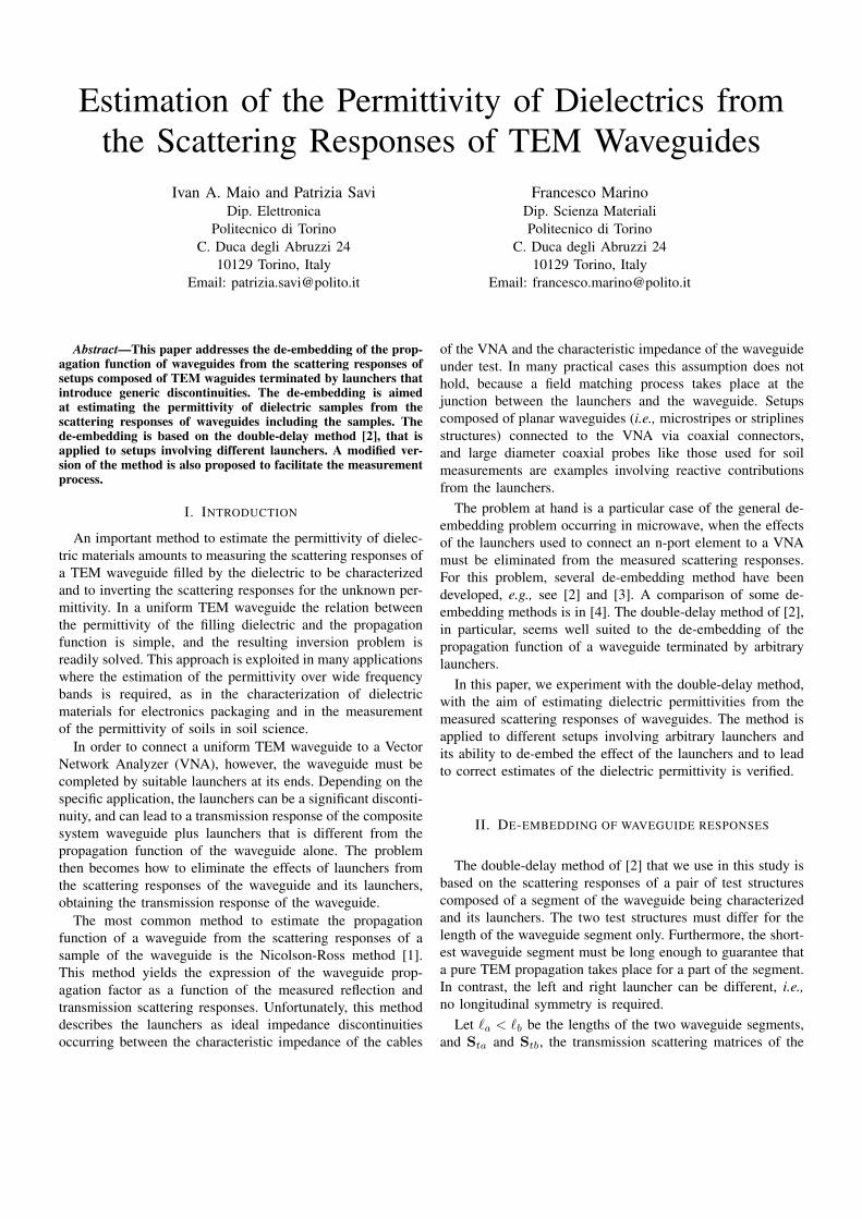
In order to test the operation and the robustness of theestimation of the propagation function via the double-delaymethod, we start by applying it to the virtual setup of Fig. 1,that is composed of an ideal LC transmission line and two ca-pacitors. The parameter of the setup are set to Yo = 1/50 Ω−1
(as in an ideal VNA), Y = 1/60 Ω−1 and τ = 0.3 ns, whereτ is the line delay.
C1 C2
Y ! YoYo
Fig. 1. Setup for the numerical test of de-embedding via the double-delaymethod. Y and τ are the characteristic admittance of the LC transmissionline whose propagation function is being estimated, Yo is the characteristicadmittance of the virtual measurement system.
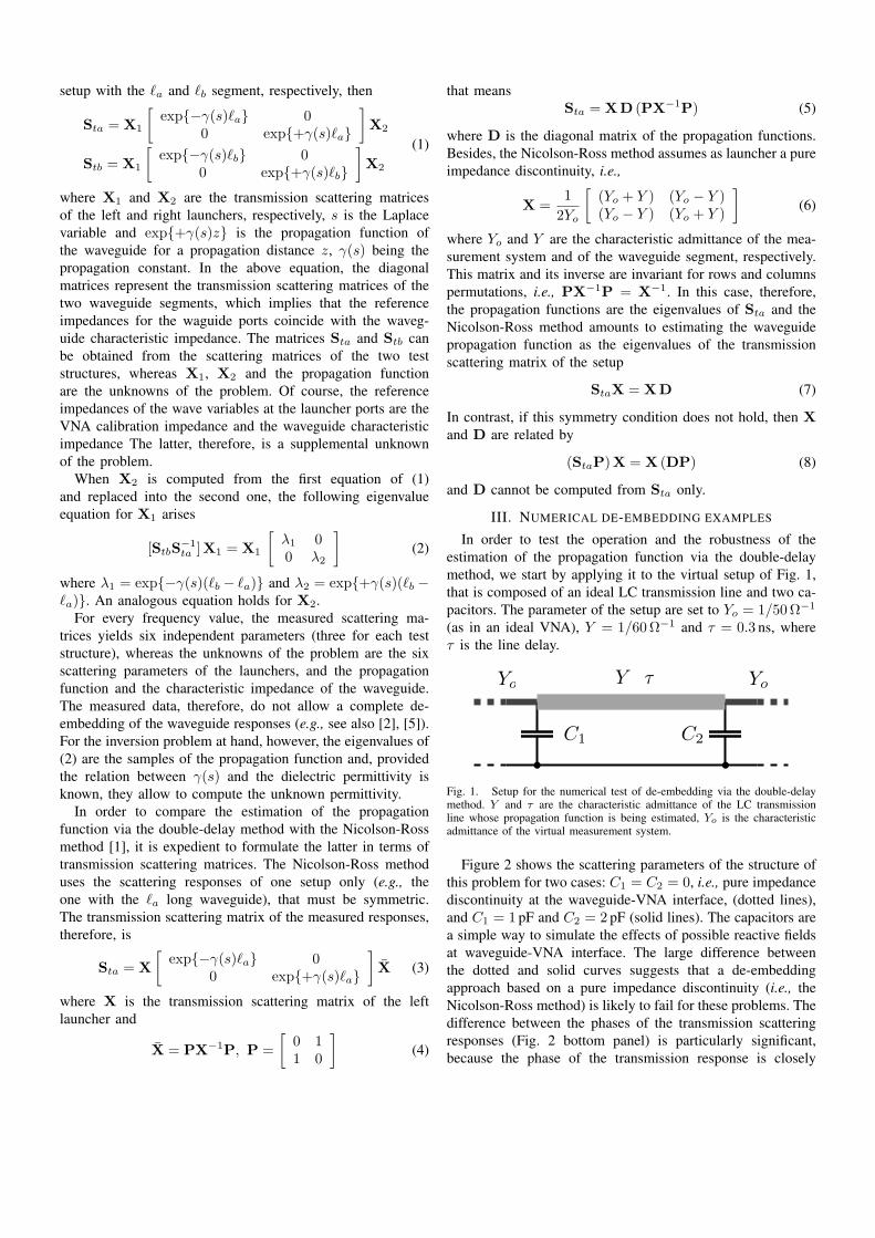
Figure 2 shows the scattering parameters of the structure ofthis problem for two cases: C1 = C2 = 0, i.e., pure impedancediscontinuity at the waveguide-VNA interface, (dotted lines),and C1 = 1 pF and C2 = 2 pF (solid lines). The capacitors area simple way to simulate the effects of possible reactive fieldsat waveguide-VNA interface. The large difference betweenthe dotted and solid curves suggests that a de-embeddingapproach based on a pure impedance discontinuity (i.e., theNicolson-Ross method) is likely to fail for these problems. Thedifference between the phases of the transmission scatteringresponses (Fig. 2 bottom panel) is particularly significant,because the phase of the transmission response is closely
related to the waveguide propagation constant and when thecapacitors are included the phase is no longer linear withfrequency, as expected for pure impedance discontinuities.
|S11|, |S22|
|S12|, |S21|
!S21
Fig. 2. Magnitude (top panel) and phase (rad, bottom panel) of the scatteringfunctions of the test setup of Fig. 1. Dotted lines hold for pure impedancediscontinuities at the waveguide-VNA juntions (C1 = C2 = 0), solid linesfor discontinuities with capacitive effects (C1 = 1 pF and C2 = 2 pF).
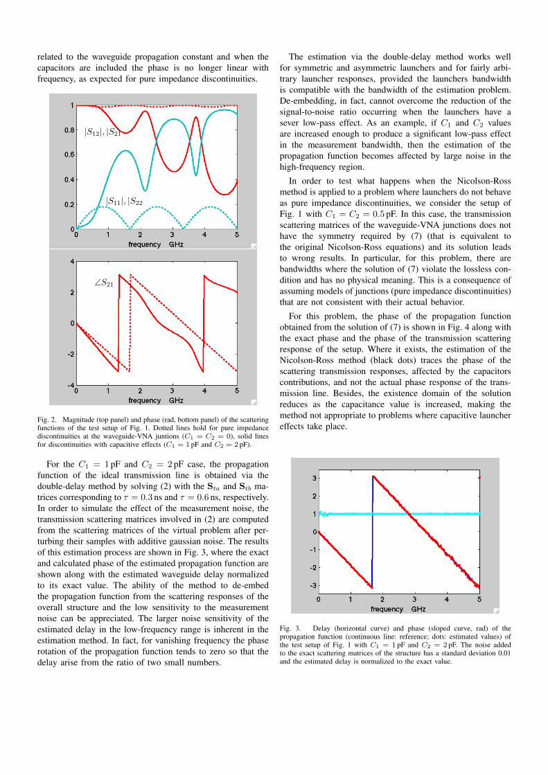
For the C1 = 1 pF and C2 = 2 pF case, the propagationfunction of the ideal transmission line is obtained via thedouble-delay method by solving (2) with the Sta and Stb ma-trices corresponding to τ = 0.3 ns and τ = 0.6 ns, respectively.In order to simulate the effect of the measurement noise, thetransmission scattering matrices involved in (2) are computedfrom the scattering matrices of the virtual problem after per-turbing their samples with additive gaussian noise. The resultsof this estimation process are shown in Fig. 3, where the exactand calculated phase of the estimated propagation function areshown along with the estimated waveguide delay normalizedto its exact value. The ability of the method to de-embedthe propagation function from the scattering responses of theoverall structure and the low sensitivity to the measurementnoise can be appreciated. The larger noise sensitivity of theestimated delay in the low-frequency range is inherent in theestimation method. In fact, for vanishing frequency the phaserotation of the propagation function tends to zero so that thedelay arise from the ratio of two small numbers.
The estimation via the double-delay method works wellfor symmetric and asymmetric launchers and for fairly arbi-trary launcher responses, provided the launchers bandwidthis compatible with the bandwidth of the estimation problem.De-embedding, in fact, cannot overcome the reduction of thesignal-to-noise ratio occurring when the launchers have asever low-pass effect. As an example, if C1 and C2 valuesare increased enough to produce a significant low-pass effectin the measurement bandwidth, then the estimation of thepropagation function becomes affected by large noise in thehigh-frequency region.
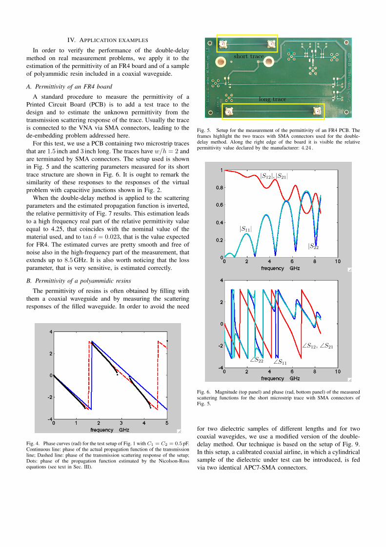
In order to test what happens when the Nicolson-Rossmethod is applied to a problem where launchers do not behaveas pure impedance discontinuities, we consider the setup ofFig. 1 with C1 = C2 = 0.5 pF. In this case, the transmissionscattering matrices of the waveguide-VNA junctions does nothave the symmetry required by (7) (that is equivalent tothe original Nicolson-Ross equations) and its solution leadsto wrong results. In particular, for this problem, there arebandwidths where the solution of (7) violate the lossless con-dition and has no physical meaning. This is a consequence ofassuming models of junctions (pure impedance discontinuities)that are not consistent with their actual behavior.
For this problem, the phase of the propagation functionobtained from the solution of (7) is shown in Fig. 4 along withthe exact phase and the phase of the transmission scatteringresponse of the setup. Where it exists, the estimation of theNicolson-Ross method (black dots) traces the phase of thescattering transmission responses, affected by the capacitorscontributions, and not the actual phase response of the trans-mission line. Besides, the existence domain of the solutionreduces as the capacitance value is increased, making themethod not appropriate to problems where capacitive launchereffects take place.
Fig. 3. Delay (horizontal curve) and phase (sloped curve, rad) of thepropagation function (continuous line: reference; dots: estimated values) ofthe test setup of Fig. 1 with C1 = 1 pF and C2 = 2 pF. The noise addedto the exact scattering matrices of the structure has a standard deviation 0.01and the estimated delay is normalized to the exact value.
IV. APPLICATION EXAMPLES
In order to verify the performance of the double-delaymethod on real measurement problems, we apply it to theestimation of the permittivity of an FR4 board and of a sampleof polyammidic resin included in a coaxial waveguide.
A. Permittivity of an FR4 board
A standard procedure to measure the permittivity of aPrinted Circuit Board (PCB) is to add a test trace to thedesign and to estimate the unknown permittivity from thetransmission scattering response of the trace. Usually the traceis connected to the VNA via SMA connectors, leading to thede-embedding problem addressed here.
For this test, we use a PCB containing two microstrip tracesthat are 1.5 inch and 3 inch long. The traces have w/h = 2 andare terminated by SMA connectors. The setup used is shownin Fig. 5 and the scattering parameters measured for its shorttrace structure are shown in Fig. 6. It is ought to remark thesimilarity of these responses to the responses of the virtualproblem with capacitive junctions shown in Fig. 2.
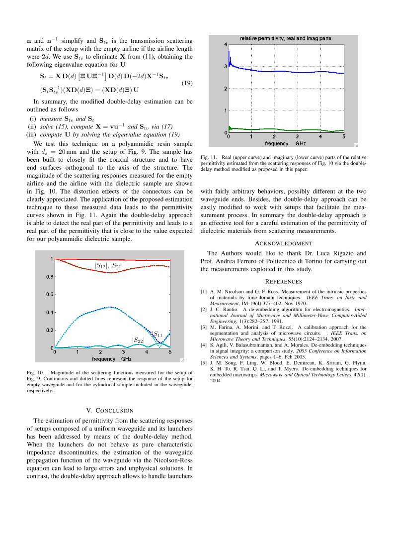
When the double-delay method is applied to the scatteringparameters and the estimated propagation function is inverted,the relative permittivity of Fig. 7 results. This estimation leadsto a high frequency real part of the relative permittivity valueequal to 4.25, that coincides with the nominal value of thematerial used, and to tan δ = 0.023, that is the value expectedfor FR4. The estimated curves are pretty smooth and free ofnoise also in the high-frequency part of the measurement, thatextends up to 8.5 GHz. It is also worth noticing that the lossparameter, that is very sensitive, is estimated correctly.
B. Permittivity of a polyammidic resins
The permittivity of resins is often obtained by filling withthem a coaxial waveguide and by measuring the scatteringresponses of the filled waveguide. In order to avoid the need
Fig. 4. Phase curves (rad) for the test setup of Fig. 1 with C1 = C2 = 0.5 pF.Continuous line: phase of the actual propagation function of the transmissionline; Dashed line: phase of the transmission scattering response of the setup;Dots: phase of the propagation function estimated by the Nicolson-Rossequations (see text in Sec. III).
short trace
long trace
Fig. 5. Setup for the measurement of the permittivity of an FR4 PCB. Theframes highlight the two traces with SMA connectors used for the double-delay method. Along the right edge of the board it is visible the relativepermittivity value declared by the manufacturer: 4.24 .
|S12|, |S21|
|S22|
|S11|
!S12, !S21
!S11!S22
Fig. 6. Magnitude (top panel) and phase (rad, bottom panel) of the measuredscattering functions for the short microstrip trace with SMA connectors ofFig. 5.
for two dielectric samples of different lengths and for twocoaxial wavegides, we use a modified version of the double-delay method. Our technique is based on the setup of Fig. 9.In this setup, a calibrated coaxial airline, in which a cylindricalsample of the dielectric under test can be introduced, is fedvia two identical APC7-SMA connectors.
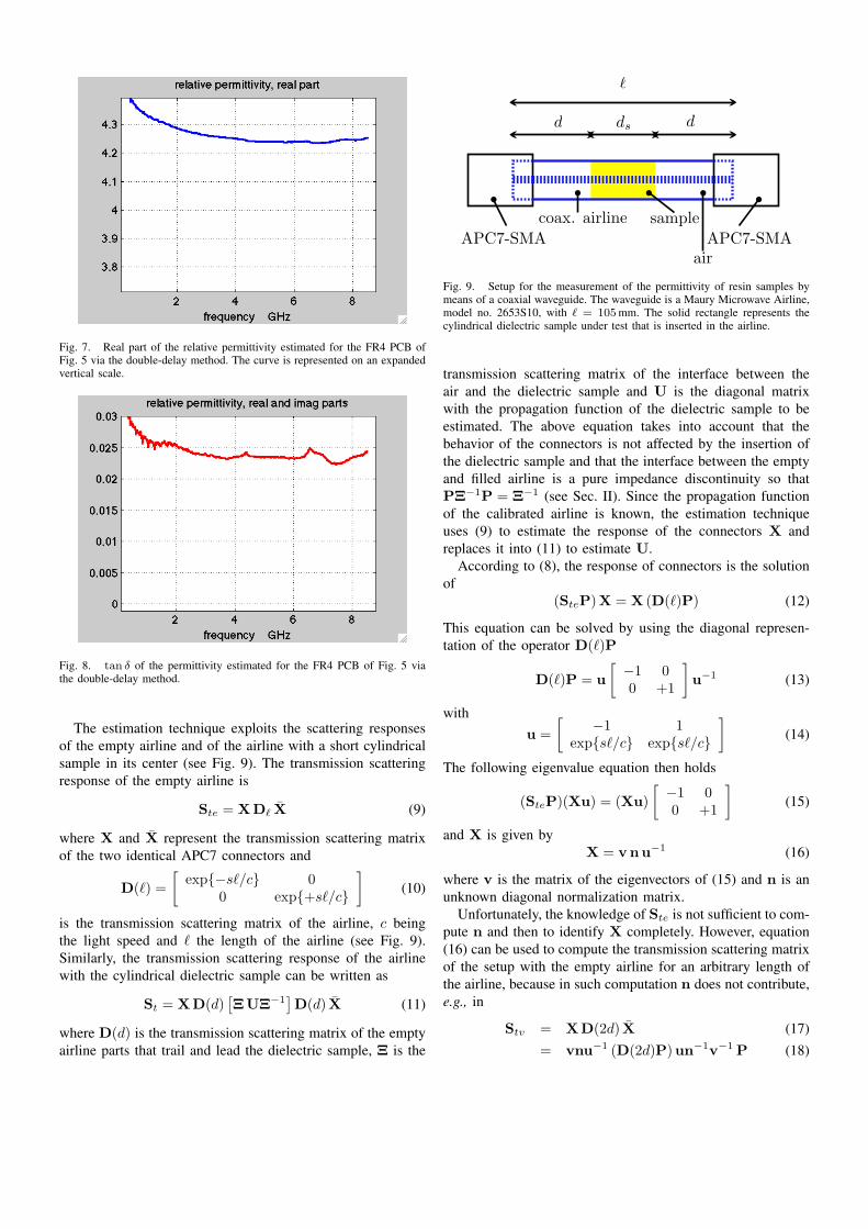
Fig. 7. Real part of the relative permittivity estimated for the FR4 PCB ofFig. 5 via the double-delay method. The curve is represented on an expandedvertical scale.
Fig. 8. tan δ of the permittivity estimated for the FR4 PCB of Fig. 5 viathe double-delay method.
The estimation technique exploits the scattering responsesof the empty airline and of the airline with a short cylindricalsample in its center (see Fig. 9). The transmission scatteringresponse of the empty airline is
Ste = X D` X (9)
where X and X represent the transmission scattering matrixof the two identical APC7 connectors and
D(`) =[
exp−s`/c 00 exp+s`/c
](10)
is the transmission scattering matrix of the airline, c beingthe light speed and ` the length of the airline (see Fig. 9).Similarly, the transmission scattering response of the airlinewith the cylindrical dielectric sample can be written as
St = X D(d)[Ξ UΞ−1
]D(d) X (11)
where D(d) is the transmission scattering matrix of the emptyairline parts that trail and lead the dielectric sample, Ξ is the
APC7-SMA APC7-SMAcoax. airline sample
!
d dds
air
Fig. 9. Setup for the measurement of the permittivity of resin samples bymeans of a coaxial waveguide. The waveguide is a Maury Microwave Airline,model no. 2653S10, with ` = 105 mm. The solid rectangle represents thecylindrical dielectric sample under test that is inserted in the airline.
transmission scattering matrix of the interface between theair and the dielectric sample and U is the diagonal matrixwith the propagation function of the dielectric sample to beestimated. The above equation takes into account that thebehavior of the connectors is not affected by the insertion ofthe dielectric sample and that the interface between the emptyand filled airline is a pure impedance discontinuity so thatPΞ−1P = Ξ−1 (see Sec. II). Since the propagation functionof the calibrated airline is known, the estimation techniqueuses (9) to estimate the response of the connectors X andreplaces it into (11) to estimate U.
According to (8), the response of connectors is the solutionof
(SteP) X = X (D(`)P) (12)
This equation can be solved by using the diagonal represen-tation of the operator D(`)P
D(`)P = u[−1 00 +1
]u−1 (13)
withu =
[−1 1
exps`/c exps`/c
](14)
The following eigenvalue equation then holds
(SteP)(Xu) = (Xu)[−1 00 +1
](15)
and X is given byX = v n u−1 (16)
where v is the matrix of the eigenvectors of (15) and n is anunknown diagonal normalization matrix.
Unfortunately, the knowledge of Ste is not sufficient to com-pute n and then to identify X completely. However, equation(16) can be used to compute the transmission scattering matrixof the setup with the empty airline for an arbitrary length ofthe airline, because in such computation n does not contribute,e.g., in
Stv = X D(2d) X (17)= vnu−1 (D(2d)P) un−1v−1 P (18)
n and n−1 simplify and Stv is the transmission scatteringmatrix of the setup with the empty airline if the airline lengthwere 2d. We use Stv to eliminate X from (11), obtaining thefollowing eigenvalue equation for U
St = X D(d)[Ξ UΞ−1
]D(d) D(−2d)X−1Stv
(StS−1tv )(XD(d)Ξ) = (XD(d)Ξ) U
(19)
In summary, the modified double-delay estimation can beoutlined as follows(i) measure Ste and St
(ii) solve (15), compute X = vu−1 and Stv via (17)(iii) compute U by solving the eigenvalue equation (19)
We test this technique on a polyammidic resin samplewith ds = 20 mm and the setup of Fig. 9. The sample hasbeen built to closely fit the coaxial structure and to haveend surfaces orthogonal to the axis of the structure. Themagnitude of the scattering responses measured for the emptyairline and the airline with the dielectric sample are shownin Fig. 10. The distortion effects of the connectors can beclearly appreciated. The application of the proposed estimationtechnique to these measured data leads to the permittivitycurves shown in Fig. 11. Again the double-delay approachis able to detect the real part of the permittivity and leads to areal part of the permittivity that is close to the value expectedfor our polyammidic dielectric sample.
|S12|, |S21|
|S22||S11|
Fig. 10. Magnitude of the scattering functions measured for the setup ofFig. 9. Continuous and dotted lines represent the response of the setup forempty waveguide and for the cylindrical sample included in the waveguide,respectively.
V. CONCLUSION
The estimation of permittivity from the scattering responsesof setups composed of a uniform waveguide and its launchershas been addressed by means of the double-delay method.When the launchers do not behave as pure characteristicimpedance discontinuities, the estimation of the waveguidepropagation function of the waveguide via the Nicolson-Rossequation can lead to large errors and unphysical solutions. Incontrast, the double-delay approach allows to handle launchers
Fig. 11. Real (upper curve) and imaginary (lower curve) parts of the relativepermittivity estimated from the scattering responses of Fig. 10 via the double-delay method modified as proposed in this paper.
with fairly arbitrary behaviors, possibly different at the twowaveguide ends. Besides, the double-delay approach can beeasily modified to work with setups that facilitate the mea-surement process. In summary the double-delay approach isan effective tool for a careful estimation of the permittivity ofdielectric materials from scattering measurements.
ACKNOWLEDGMENT
The Authors would like to thank Dr. Luca Rigazio andProf. Andrea Ferrero of Politecnico di Torino for carrying outthe measurements exploited in this study.
REFERENCES
[1] A. M. Nicolson and G. F. Ross. Measurement of the intrinsic propertiesof materials by time-domain techniques. IEEE Trans. on Instr. andMeasurement, IM-19(4):377–402, Nov 1970.
[2] J. C. Rautio. A de-embedding algorithm for electromagnetics. Inter-national Journal of Microwave and Millimeter-Wave Computer-AidedEngineering, 1(3):282–2S7, 1991.
[3] M. Farina, A. Morini, and T. Rozzi. A calibration approach for thesegmentation and analysis of microwave circuits. , IEEE Trans. onMicrowave Theory and Techniques, 55(10):2124–2134, 2007.
[4] S. Agili, V. Balasubramanian, and A. Morales. De-embedding techniquesin signal integrity: a comparison study. 2005 Conference on InformationSciences and Systems, pages 1–6, Feb 2005.
[5] J. M. Song, F. Ling, W. Blood, E. Demircan, K. Sriram, G. Flynn,K. H. To, R. Tsai, Q. Li, and T. Myers. De-embedding techniques forembedded microstrips. Microwave and Optical Technology Letters, 42(1),2004.


