Embed Size (px)
Citation preview
Direct Detection TEM Cameras
FOR MORE INFORMATION:BENJAMIN BAMMES, Ph.D.
DIRECTOR OF APPLICATIONS, MARKETING, & SALESEMAIL: [email protected]
PHONE: +1 858-384-0291 x105SKYPE: bbammes
CONFIDENTIAL: Do not share or distribute without written permission.Copyright © 2017 Direct Electron, LP. All rights reserved.
Slide #2 November 201
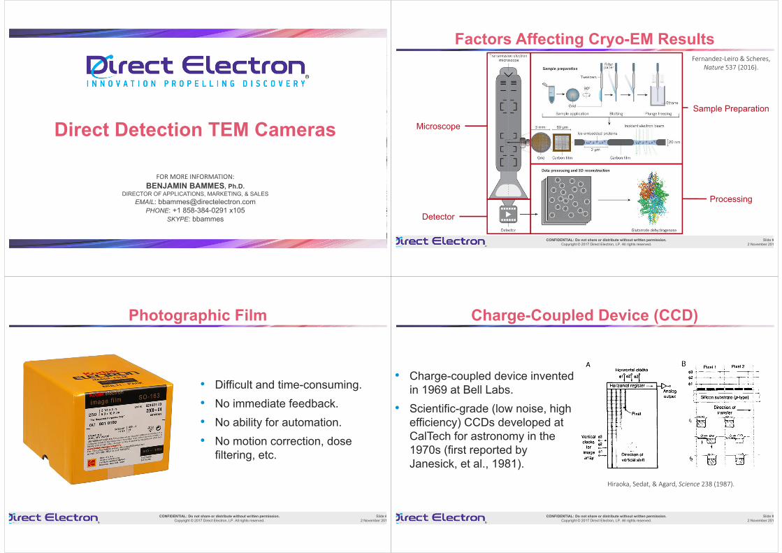
Factors Affecting Cryo-EM ResultsFernandez-Leiro & Scheres,
Nature 537 (2016).
Microscope
Detector
Sample Preparation
Processing
CONFIDENTIAL: Do not share or distribute without written permission.Copyright © 2017 Direct Electron, LP. All rights reserved.
Slide #2 November 201
Photographic Film
• Difficult and time-consuming.• No immediate feedback.• No ability for automation.• No motion correction, dose
filtering, etc.
CONFIDENTIAL: Do not share or distribute without written permission.Copyright © 2017 Direct Electron, LP. All rights reserved.
Slide #2 November 201
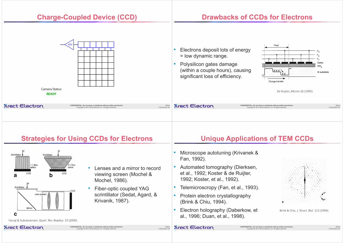
Charge-Coupled Device (CCD)
• Charge-coupled device invented in 1969 at Bell Labs.
• Scientific-grade (low noise, high efficiency) CCDs developed at CalTech for astronomy in the 1970s (first reported by Janesick, et al., 1981).
Hiraoka, Sedat, & Agard, Science 238 (1987).
CONFIDENTIAL: Do not share or distribute without written permission.Copyright © 2017 Direct Electron, LP. All rights reserved.
Slide #2 November 201
Charge-Coupled Device (CCD)
CONFIDENTIAL: Do not share or distribute without written permission.Copyright © 2017 Direct Electron, LP. All rights reserved.
Slide #2 November 201
Drawbacks of CCDs for Electrons
• Electrons deposit lots of energy = low dynamic range.
• Polysilicon gates damage (within a couple hours), causing significant loss of efficiency.
De Ruijter, Micron 26 (1995).
CONFIDENTIAL: Do not share or distribute without written permission.Copyright © 2017 Direct Electron, LP. All rights reserved.
Slide #2 November 201
Strategies for Using CCDs for Electrons
• Lenses and a mirror to record viewing screen (Mochel & Mochel, 1986).
• Fiber-optic coupled YAG scrintillator (Sedat, Agard, & Krivanik, 1987).
Faruqi & Subramaniam, Quart. Rev. Biophys. 33 (2000).
CONFIDENTIAL: Do not share or distribute without written permission.Copyright © 2017 Direct Electron, LP. All rights reserved.
Slide #2 November 201
Unique Applications of TEM CCDs
• Microscope autotuning (Krivanek & Fan, 1992).
• Automated tomography (Dierksen, et al., 1992; Koster & de Ruijter, 1992; Koster, et al., 1992).
• Telemicroscropy (Fan, et al., 1993).• Protein electron crystallography
(Brink & Chiu, 1994).• Electron holography (Daberkow, et
al., 1996; Duan, et al., 1998).Brink & Chiu, J. Struct. Biol. 113 (1994).
CONFIDENTIAL: Do not share or distribute without written permission.Copyright © 2017 Direct Electron, LP. All rights reserved.
Slide #2 November 201
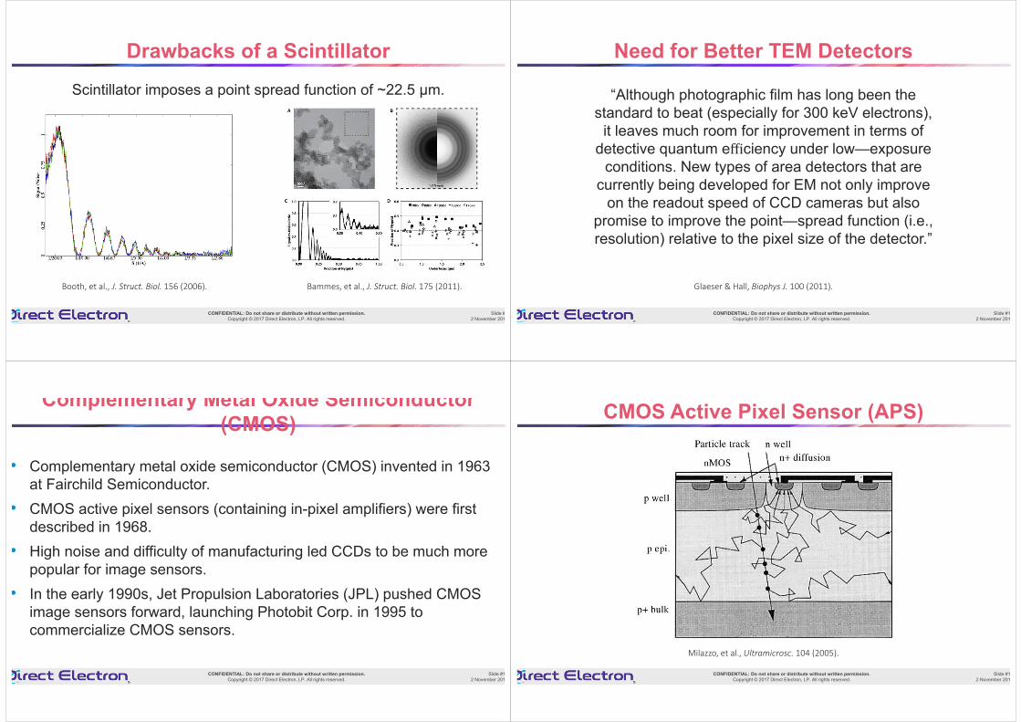
Drawbacks of a Scintillator
Booth, et al., J. Struct. Biol. 156 (2006). Bammes, et al., J. Struct. Biol. 175 (2011).
Scintillator imposes a point spread function of ~22.5 μm.
CONFIDENTIAL: Do not share or distribute without written permission.Copyright © 2017 Direct Electron, LP. All rights reserved.
Slide #12 November 201
Need for Better TEM Detectors
Glaeser & Hall, Biophys J. 100 (2011).
“Although photographic film has long been the standard to beat (especially for 300 keV electrons),
it leaves much room for improvement in terms of detective quantum efficiency under low—exposure
conditions. New types of area detectors that are currently being developed for EM not only improve
on the readout speed of CCD cameras but also promise to improve the point—spread function (i.e., resolution) relative to the pixel size of the detector.”
CONFIDENTIAL: Do not share or distribute without written permission.Copyright © 2017 Direct Electron, LP. All rights reserved.
Slide #12 November 201
Complementary Metal Oxide Semiconductor (CMOS)
• Complementary metal oxide semiconductor (CMOS) invented in 1963 at Fairchild Semiconductor.
• CMOS active pixel sensors (containing in-pixel amplifiers) were first described in 1968.
• High noise and difficulty of manufacturing led CCDs to be much more popular for image sensors.
• In the early 1990s, Jet Propulsion Laboratories (JPL) pushed CMOS image sensors forward, launching Photobit Corp. in 1995 to commercialize CMOS sensors.
CONFIDENTIAL: Do not share or distribute without written permission.Copyright © 2017 Direct Electron, LP. All rights reserved.
Slide #12 November 201
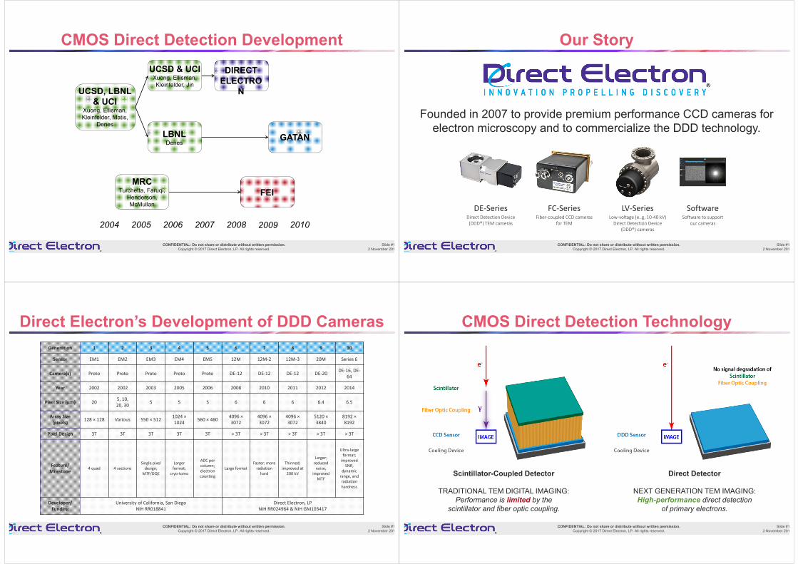
CMOS Active Pixel Sensor (APS)
Milazzo, et al., Ultramicrosc. 104 (2005).
CONFIDENTIAL: Do not share or distribute without written permission.Copyright © 2017 Direct Electron, LP. All rights reserved.
Slide #12 November 201
CMOS Direct Detection DevelopmentUCSD & UCI
Xuong, Ellisman, Kleinfelder, Jin
MRCTurchetta, Faruqi,
Henderson, McMullan
UCSD, LBNL & UCI
Xuong, Ellisman, Kleinfelder, Matis,
Denes
LBNLDenes
DIRECT ELECTRO
N
GATAN
FEI
20052004 2006 2007 2008 2009 2010
CONFIDENTIAL: Do not share or distribute without written permission.Copyright © 2017 Direct Electron, LP. All rights reserved.
Slide #12 November 201
Our Story
Founded in 2007 to provide premium performance CCD cameras for electron microscopy and to commercialize the DDD technology.
DE-Series FC-Series LV-Series SoftwareDirect Detection Device
(DDD®) TEM camerasFiber-coupled CCD cameras
for TEMLow-voltage (e..g, 10-40 kV)
Direct Detection Device (DDD®) cameras
Software to supportour cameras
CONFIDENTIAL: Do not share or distribute without written permission.Copyright © 2017 Direct Electron, LP. All rights reserved.
Slide #12 November 201
Direct Electron’s Development of DDD CamerasGeneration 1 2 3 4 5 6 7 8 9 10
Sensor EM1 EM2 EM3 EM4 EM5 12M 12M-2 12M-3 20M Series 6
Camera(s) Proto Proto Proto Proto Proto DE-12 DE-12 DE-12 DE-20 DE-16, DE-64
Year 2002 2002 2003 2005 2006 2008 2010 2011 2012 2014
Pixel Size (μm) 20 5, 10,20, 30 5 5 5 6 6 6 6.4 6.5
Array Size (pixels) 128 × 128 Various 550 × 512 1024 ×
1024 560 × 460 4096 ×3072
4096 ×3072
4096 ×3072
5120 ×3840
8192 ×8192
Pixel Design 3T 3T 3T 3T 3T > 3T > 3T > 3T > 3T > 3T
Feature/Milestone
4 quad 4 sectionsSingle pixel
design; MTF/DQE
Largerformat;
cryo-tomo
ADC per column; electron counting
Large formatFaster; more
radiation hard
Thinned; improved at
200 kV
Larger;reduced noise;
improved MTF
Ultra-largeformat;
improved SNR,
dynamic range, and radiation hardness
Developer/Funding
University of California, San DiegoNIH RR018841
Direct Electron, LPNIH RR024964 & NIH GM103417
CONFIDENTIAL: Do not share or distribute without written permission.Copyright © 2017 Direct Electron, LP. All rights reserved.
Slide #12 November 201
CMOS Direct Detection Technology
Scintillator-Coupled Detector
TRADITIONAL TEM DIGITAL IMAGING:Performance is limited by the
scintillator and fiber optic coupling.
Direct Detector
NEXT GENERATION TEM IMAGING:High-performance direct detection
of primary electrons.
CONFIDENTIAL: Do not share or distribute without written permission.Copyright © 2017 Direct Electron, LP. All rights reserved.
Slide #12 November 201
Resolution (Edge Spread Function)
CONFIDENTIAL: Do not share or distribute without written permission.Copyright © 2017 Direct Electron, LP. All rights reserved.
Slide #12 November 201
Missing Features on a Scintillator-Coupled Camera
CONFIDENTIAL: Do not share or distribute without written permission.Copyright © 2017 Direct Electron, LP. All rights reserved.
Slide #12 November 201
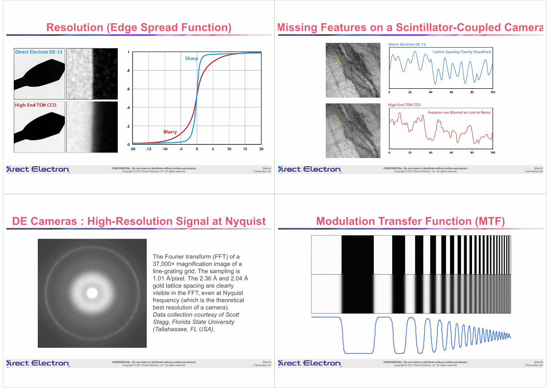
DE Cameras : High-Resolution Signal at Nyquist
The Fourier transform (FFT) of a 37,000× magnification image of a line-grating grid. The sampling is 1.01 Å/pixel. The 2.36 Å and 2.04 Ågold lattice spacing are clearly visible in the FFT, even at Nyquist frequency (which is the theoreticalbest resolution of a camera).Data collection courtesy of Scott Stagg, Florida State University (Tallahassee, FL USA).
CONFIDENTIAL: Do not share or distribute without written permission.Copyright © 2017 Direct Electron, LP. All rights reserved.
Slide #22 November 201
Modulation Transfer Function (MTF)
CONFIDENTIAL: Do not share or distribute without written permission.Copyright © 2017 Direct Electron, LP. All rights reserved.
Slide #22 November 201
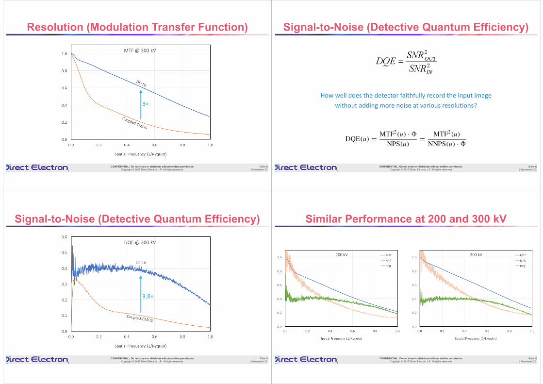
Resolution (Modulation Transfer Function)
CONFIDENTIAL: Do not share or distribute without written permission.Copyright © 2017 Direct Electron, LP. All rights reserved.
Slide #22 November 201
Signal-to-Noise (Detective Quantum Efficiency)
How well does the detector faithfully record the input imagewithout adding more noise at various resolutions?
CONFIDENTIAL: Do not share or distribute without written permission.Copyright © 2017 Direct Electron, LP. All rights reserved.
Slide #22 November 201
Signal-to-Noise (Detective Quantum Efficiency)
CONFIDENTIAL: Do not share or distribute without written permission.Copyright © 2017 Direct Electron, LP. All rights reserved.
Slide #22 November 201
Similar Performance at 200 and 300 kV
CONFIDENTIAL: Do not share or distribute without written permission.Copyright © 2017 Direct Electron, LP. All rights reserved.
Slide #22 November 201
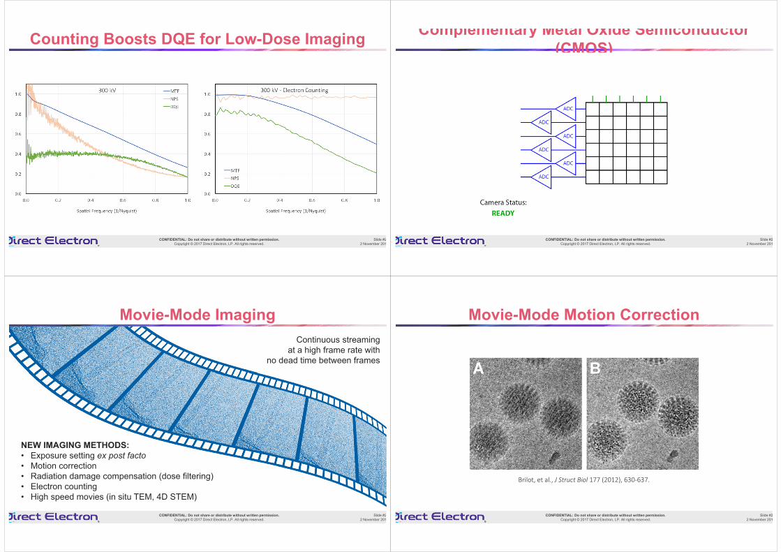
Counting Boosts DQE for Low-Dose Imaging
CONFIDENTIAL: Do not share or distribute without written permission.Copyright © 2017 Direct Electron, LP. All rights reserved.
Slide #22 November 201
Complementary Metal Oxide Semiconductor (CMOS)
CONFIDENTIAL: Do not share or distribute without written permission.Copyright © 2017 Direct Electron, LP. All rights reserved.
Slide #22 November 201
Movie-Mode Imaging
NEW IMAGING METHODS:• Exposure setting ex post facto• Motion correction• Radiation damage compensation (dose filtering)• Electron counting• High speed movies (in situ TEM, 4D STEM)
Continuous streamingat a high frame rate with
no dead time between frames
CONFIDENTIAL: Do not share or distribute without written permission.Copyright © 2017 Direct Electron, LP. All rights reserved.
Slide #22 November 201
Movie-Mode Motion Correction
Brilot, et al., J Struct Biol 177 (2012), 630-637.
CONFIDENTIAL: Do not share or distribute without written permission.Copyright © 2017 Direct Electron, LP. All rights reserved.
Slide #22 November 201
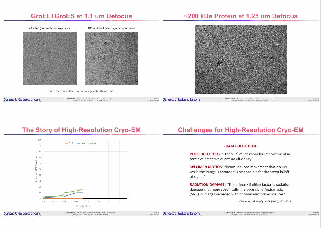
GroEL+GroES at 1.1 um Defocus20 e-/Å2 (conventional exposure) 100 e-/Å2 with damage compensation
Courtesy of Wah Chiu, Baylor College of Medicine, USA.
CONFIDENTIAL: Do not share or distribute without written permission.Copyright © 2017 Direct Electron, LP. All rights reserved.
Slide #32 November 201
~200 kDa Protein at 1.25 um Defocus
CONFIDENTIAL: Do not share or distribute without written permission.Copyright © 2017 Direct Electron, LP. All rights reserved.
Slide #32 November 201
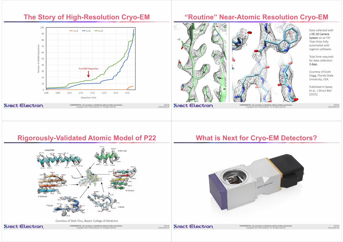
The Story of High-Resolution Cryo-EM
0
10
20
30
40
50
60
70
80
90
100
1/08 1/09 1/10 1/11 1/12 1/13 1/14 1/15
Num
ber o
f EM
DB D
epos
ition
s
Deposition Date
2.x Å 3.x Å 4.x Å
CONFIDENTIAL: Do not share or distribute without written permission.Copyright © 2017 Direct Electron, LP. All rights reserved.
Slide #32 November 201
Challenges for High-Resolution Cryo-EM
- DATA COLLECTION -
POOR DETECTORS: “[There is] much room for improvement in terms of detective quantum efficiency.”
SPECIMEN MOTION: “Beam-induced movement that occurs while the image is recorded is responsible for the steep falloff of signal.”
RADIATION DAMAGE: “The primary limiting factor is radiation damage and, more specifically, the poor signal/noise ratio (SNR) in images recorded with optimal electron exposures.”
Glaeser & Hall, Biophys J 100 (2011), 2331-2337.
CONFIDENTIAL: Do not share or distribute without written permission.Copyright © 2017 Direct Electron, LP. All rights reserved.
Slide #32 November 201
The Story of High-Resolution Cryo-EM
First DDD Deposition
0
10
20
30
40
50
60
70
80
90
100
1/08 1/09 1/10 1/11 1/12 1/13 1/14 1/15
Num
ber o
f EM
DB D
epos
ition
s
Deposition Date
2.x Å 3.x Å 4.x Å
CONFIDENTIAL: Do not share or distribute without written permission.Copyright © 2017 Direct Electron, LP. All rights reserved.
Slide #32 November 201
“Routine” Near-Atomic Resolution Cryo-EMData collected with a DE-20 Camera System on an FEI Titan Krios fully automated with Leginon software.
Total time required for data collection:3 days.
Courtesy of Scott Stagg, Florida State University, USA.
Published in Spear, et al., J Struct Biol(2015).
CONFIDENTIAL: Do not share or distribute without written permission.Copyright © 2017 Direct Electron, LP. All rights reserved.
Slide #32 November 201
Rigorously-Validated Atomic Model of P22
Courtesy of Wah Chiu, Baylor College of MedicineCONFIDENTIAL: Do not share or distribute without written permission.
Copyright © 2017 Direct Electron, LP. All rights reserved.Slide #3
2 November 201
What is Next for Cryo-EM Detectors?
CONFIDENTIAL: Do not share or distribute without written permission.Copyright © 2017 Direct Electron, LP. All rights reserved.
Slide #32 November 201
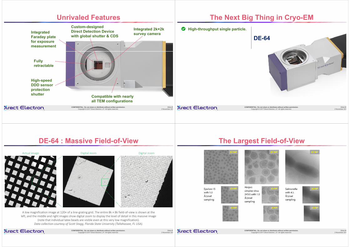
Unrivaled Features
IntegratedFaraday platefor exposuremeasurement
Integrated 2k×2ksurvey camera
Fullyretractable
High-speedDDD sensorprotectionshutter
Custom-designedDirect Detection Devicewith global shutter & CDS
Compatible with nearlyall TEM configurations
CONFIDENTIAL: Do not share or distribute without written permission.Copyright © 2017 Direct Electron, LP. All rights reserved.
Slide #32 November 201
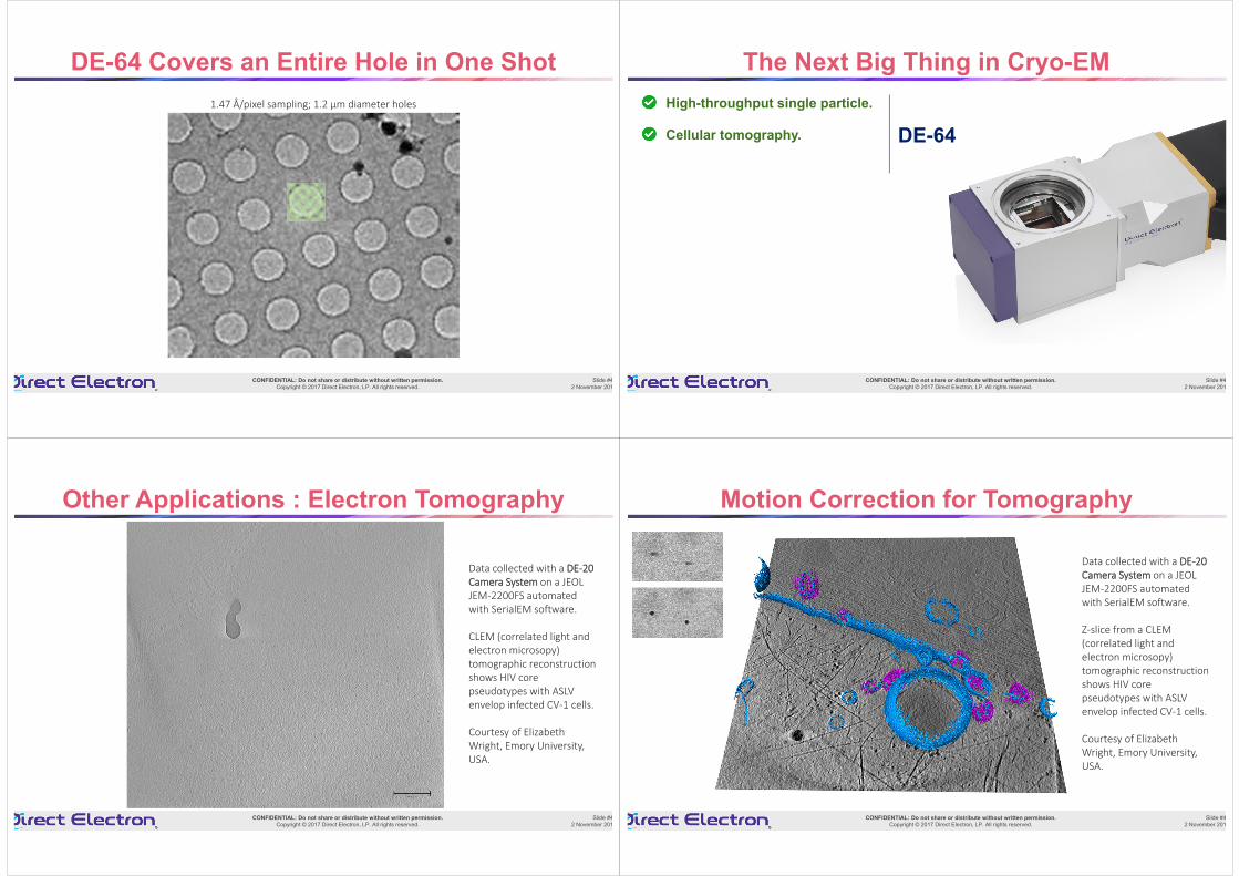
The Next Big Thing in Cryo-EMHigh-throughput single particle.
DE-64
CONFIDENTIAL: Do not share or distribute without written permission.Copyright © 2017 Direct Electron, LP. All rights reserved.
Slide #32 November 201
DE-64 : Massive Field-of-View
A low magnification image at 120× of a line-grating grid. The entire 8k × 8k field-of-view is shown at the left, and the middle and right images show digital zoom to display the level of detail in this massive image
(note that individual latex beads are visible even at this very low magnification).Data collection courtesy of Scott Stagg, Florida State University (Tallahassee, FL USA).
Digital zoom Digital zoomActual image
CONFIDENTIAL: Do not share or distribute without written permission.Copyright © 2017 Direct Electron, LP. All rights reserved.
Slide #42 November 201
The Largest Field-of-View67 MP 67 MP 67 MP
16 MP 16 MP 16 MP
14 MP 14 MP 14 MP
CONFIDENTIAL: Do not share or distribute without written permission.Copyright © 2017 Direct Electron, LP. All rights reserved.
Slide #42 November 201
DE-64 Covers an Entire Hole in One Shot1.47 Å/pixel sampling; 1.2 μm diameter holes
CONFIDENTIAL: Do not share or distribute without written permission.Copyright © 2017 Direct Electron, LP. All rights reserved.
Slide #42 November 201
The Next Big Thing in Cryo-EMHigh-throughput single particle.
Cellular tomography. DE-64
CONFIDENTIAL: Do not share or distribute without written permission.Copyright © 2017 Direct Electron, LP. All rights reserved.
Slide #42 November 201
Other Applications : Electron Tomography
Data collected with a DE-20 Camera System on a JEOL JEM-2200FS automated with SerialEM software.
CLEM (correlated light and electron microsopy) tomographic reconstruction shows HIV core pseudotypes with ASLV envelop infected CV-1 cells.
Courtesy of Elizabeth Wright, Emory University, USA.
CONFIDENTIAL: Do not share or distribute without written permission.Copyright © 2017 Direct Electron, LP. All rights reserved.
Slide #42 November 201
Motion Correction for Tomography
Data collected with a DE-20 Camera System on a JEOL JEM-2200FS automated with SerialEM software.
Z-slice from a CLEM (correlated light and electron microsopy) tomographic reconstruction shows HIV core pseudotypes with ASLV envelop infected CV-1 cells.
Courtesy of Elizabeth Wright, Emory University, USA.
CONFIDENTIAL: Do not share or distribute without written permission.Copyright © 2017 Direct Electron, LP. All rights reserved.
Slide #42 November 201
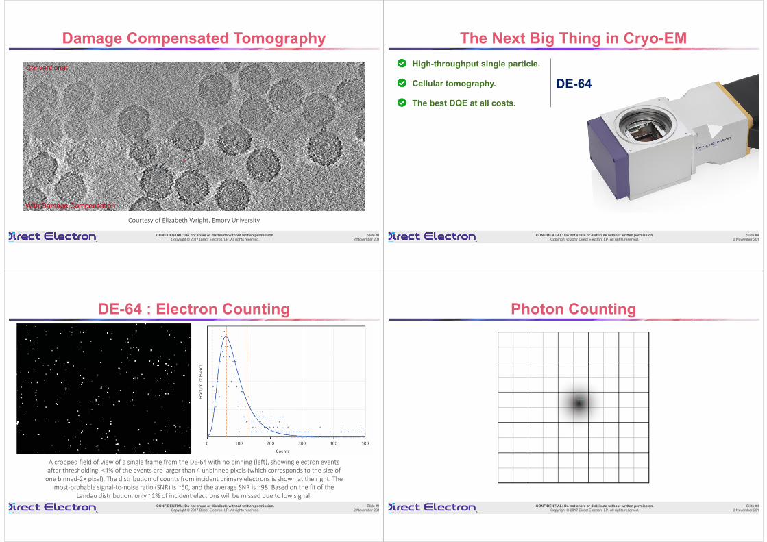
Damage Compensated Tomography
Courtesy of Elizabeth Wright, Emory University
Conventional
With Damage Compensation
CONFIDENTIAL: Do not share or distribute without written permission.Copyright © 2017 Direct Electron, LP. All rights reserved.
Slide #42 November 201
The Next Big Thing in Cryo-EMHigh-throughput single particle.
Cellular tomography. DE-64The best DQE at all costs.
CONFIDENTIAL: Do not share or distribute without written permission.Copyright © 2017 Direct Electron, LP. All rights reserved.
Slide #42 November 201
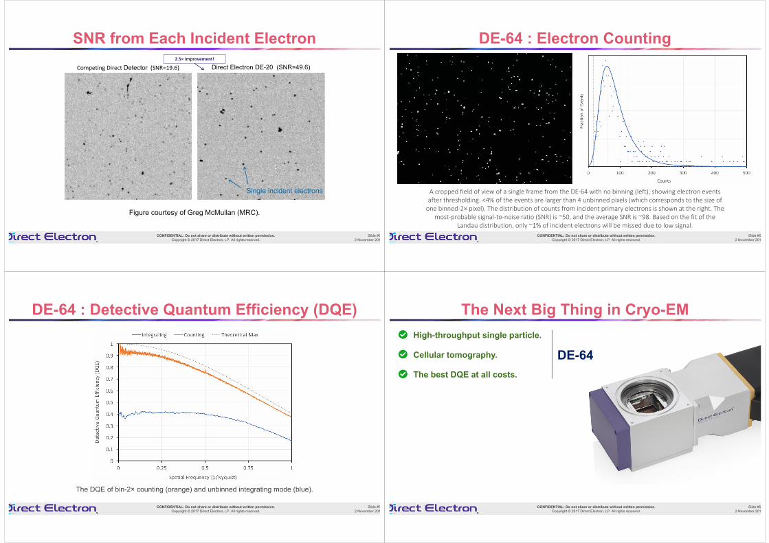
DE-64 : Electron Counting
A cropped field of view of a single frame from the DE-64 with no binning (left), showing electron events after thresholding. <4% of the events are larger than 4 unbinned pixels (which corresponds to the size of
one binned-2× pixel). The distribution of counts from incident primary electrons is shown at the right. The most-probable signal-to-noise ratio (SNR) is ~50, and the average SNR is ~98. Based on the fit of the
Landau distribution, only ~1% of incident electrons will be missed due to low signal.CONFIDENTIAL: Do not share or distribute without written permission.
Copyright © 2017 Direct Electron, LP. All rights reserved.Slide #4
2 November 201
Photon Counting
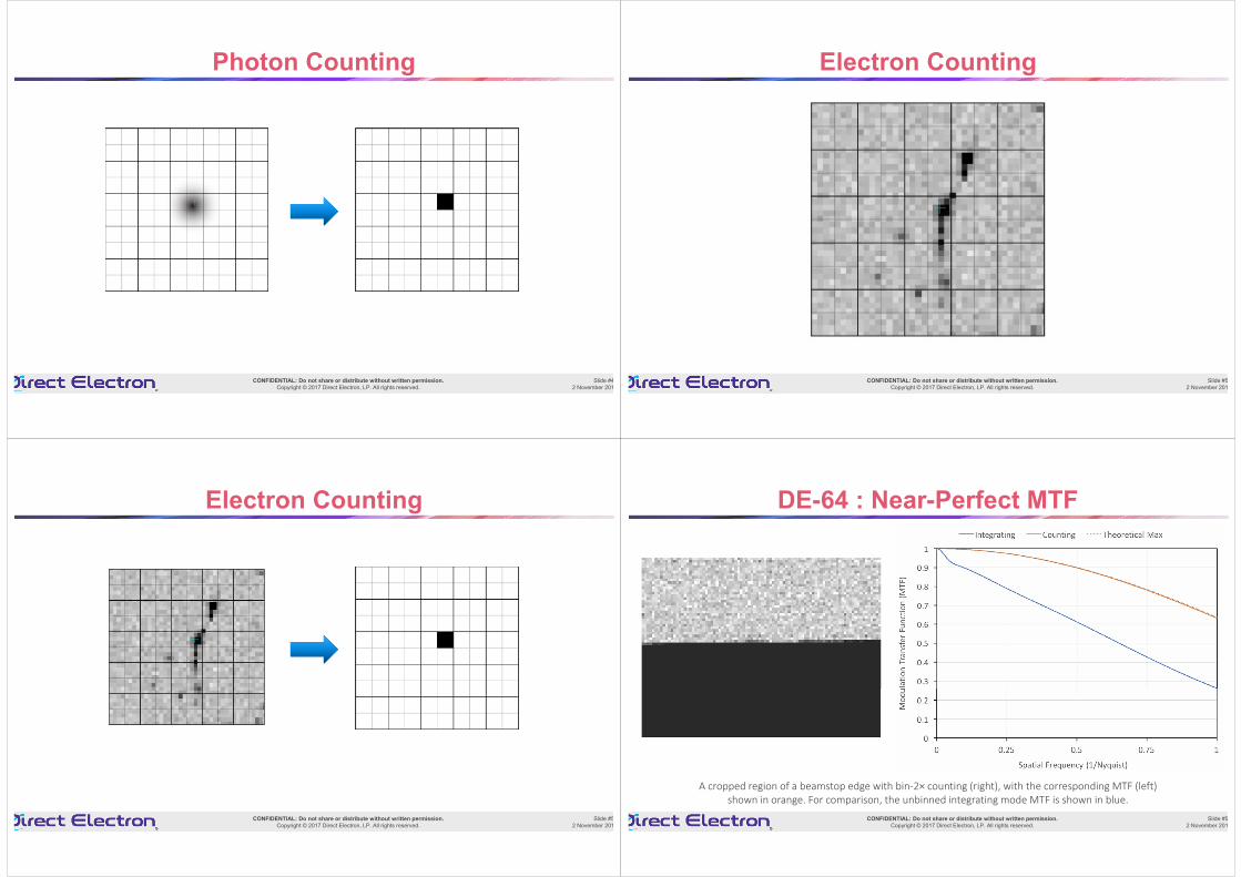
CONFIDENTIAL: Do not share or distribute without written permission.Copyright © 2017 Direct Electron, LP. All rights reserved.
Slide #42 November 201
Photon Counting
CONFIDENTIAL: Do not share or distribute without written permission.Copyright © 2017 Direct Electron, LP. All rights reserved.
Slide #52 November 201
Electron Counting
CONFIDENTIAL: Do not share or distribute without written permission.Copyright © 2017 Direct Electron, LP. All rights reserved.
Slide #52 November 201
Electron Counting
CONFIDENTIAL: Do not share or distribute without written permission.Copyright © 2017 Direct Electron, LP. All rights reserved.
Slide #52 November 201
DE-64 : Near-Perfect MTF
A cropped region of a beamstop edge with bin-2× counting (right), with the corresponding MTF (left) shown in orange. For comparison, the unbinned integrating mode MTF is shown in blue.
CONFIDENTIAL: Do not share or distribute without written permission.Copyright © 2017 Direct Electron, LP. All rights reserved.
Slide #52 November 201
SNR from Each Incident ElectronCompeting Direct Detector (SNR=19.6) Direct Electron DE-20 (SNR=49.6)
Figure courtesy of Greg McMullan (MRC).
Single incident electrons
2.5× improvement!
CONFIDENTIAL: Do not share or distribute without written permission.Copyright © 2017 Direct Electron, LP. All rights reserved.
Slide #52 November 201
DE-64 : Electron Counting
A cropped field of view of a single frame from the DE-64 with no binning (left), showing electron events after thresholding. <4% of the events are larger than 4 unbinned pixels (which corresponds to the size of
one binned-2× pixel). The distribution of counts from incident primary electrons is shown at the right. The most-probable signal-to-noise ratio (SNR) is ~50, and the average SNR is ~98. Based on the fit of the
Landau distribution, only ~1% of incident electrons will be missed due to low signal.
CONFIDENTIAL: Do not share or distribute without written permission.Copyright © 2017 Direct Electron, LP. All rights reserved.
Slide #52 November 201
DE-64 : Detective Quantum Efficiency (DQE)
The DQE of bin-2× counting (orange) and unbinned integrating mode (blue).
CONFIDENTIAL: Do not share or distribute without written permission.Copyright © 2017 Direct Electron, LP. All rights reserved.
Slide #52 November 201
The Next Big Thing in Cryo-EMHigh-throughput single particle.
Cellular tomography. DE-64The best DQE at all costs.
CONFIDENTIAL: Do not share or distribute without written permission.Copyright © 2017 Direct Electron, LP. All rights reserved.
Slide #52 November 201
The Next Big Thing in Cryo-EMHigh-throughput single particle.
Cellular tomography. DE-64The best DQE at all costs.
High-resolution at 200kV. DE-20
CONFIDENTIAL: Do not share or distribute without written permission.Copyright © 2017 Direct Electron, LP. All rights reserved.
Slide #52 November 201
Fast, High-Resolution at 200 kV (F20 TEM)A representative cryo-EM micrograph and selected 2D class averages of Thermoplasmaacidophilum 20S Proteasome imaged on a DE-20 camera on a 200 kV FEG Tecnai F20 TEM without an objective aperture. The micrograph shown is at1.5 μm defocus. A total of 350 micrographs were collected using automation in SerialEM, at a rate of approximately 80 acquisitions per hour. Pixel size = 0.91 Å/pixel.
Data courtesy of Radostin Danev, Max Planck Institute of Biochemistry (Martinsried, Germany).
CONFIDENTIAL: Do not share or distribute without written permission.Copyright © 2017 Direct Electron, LP. All rights reserved.
Slide #52 November 201
Fast, High-Resolution at 200 kV (F20 TEM)
Each acquisition contained 20 frames, which were motion corrected and dose filtered using MotionCor2 (Zheng et al., 2017) with 5×4 patches. CTF parameters were determined using CTFFind4 (Rohou & Grigorieff, 2015). Boxing was completed using EMAN2 (Tang et al., 2007). 2D class averages and the 3D reconstruction were generated using Relion (Scheres, 2012). All image processing was completed on a desktop computer with a single NVidia GeForce GTX 1060 GPU.
A total of 43,637 particles were boxed, of which 31,324 particles were retained after selecting reasonable-looking 2D class averages (examples shown above).
CONFIDENTIAL: Do not share or distribute without written permission.Copyright © 2017 Direct Electron, LP. All rights reserved.
Slide #62 November 201
Fast, High-Resolution at 200 kV (F20 TEM)
The final 3D reconstruction (shown at left) reached 3.76 Å resolution by gold-standard FSC. An alpha-helix and beta-sheet from the reconstruction are shown below, with the X-ray crystal structure (PDB: 1PMA) rigid-body fit into the cryo-EM density map.
CONFIDENTIAL: Do not share or distribute without written permission.Copyright © 2017 Direct Electron, LP. All rights reserved.
Slide #62 November 201
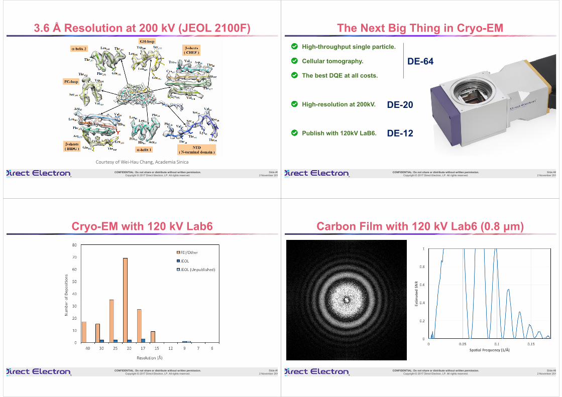
3.6 Å Resolution at 200 kV (JEOL 2100F)
Courtesy of Wei-Hau Chang, Academia Sinica
CONFIDENTIAL: Do not share or distribute without written permission.Copyright © 2017 Direct Electron, LP. All rights reserved.
Slide #62 November 201
The Next Big Thing in Cryo-EMHigh-throughput single particle.
Cellular tomography. DE-64The best DQE at all costs.
High-resolution at 200kV.
Publish with 120kV LaB6.
DE-20
DE-12
CONFIDENTIAL: Do not share or distribute without written permission.Copyright © 2017 Direct Electron, LP. All rights reserved.
Slide #62 November 201
Cryo-EM with 120 kV Lab6
CONFIDENTIAL: Do not share or distribute without written permission.Copyright © 2017 Direct Electron, LP. All rights reserved.
Slide #62 November 201
Carbon Film with 120 kV Lab6 (0.8 μm)
CONFIDENTIAL: Do not share or distribute without written permission.Copyright © 2017 Direct Electron, LP. All rights reserved.
Slide #62 November 201
Carbon Film with 120 kV Lab6 (2.3 μm)
CONFIDENTIAL: Do not share or distribute without written permission.Copyright © 2017 Direct Electron, LP. All rights reserved.
Slide #62 November 201
Carbon Film with 120 kV Lab6 (1.5 μm)
CONFIDENTIAL: Do not share or distribute without written permission.Copyright © 2017 Direct Electron, LP. All rights reserved.
Slide #62 November 201
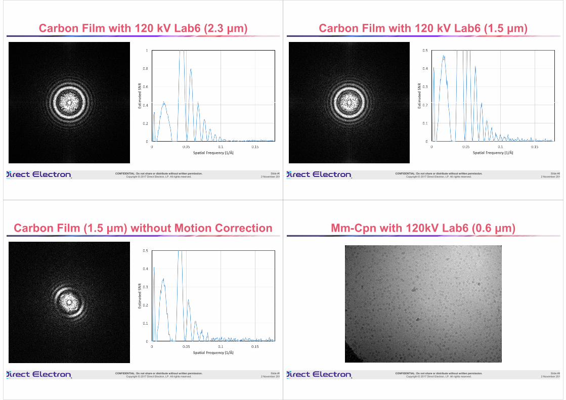
Carbon Film (1.5 μm) without Motion Correction
CONFIDENTIAL: Do not share or distribute without written permission.Copyright © 2017 Direct Electron, LP. All rights reserved.
Slide #62 November 201
Mm-Cpn with 120kV Lab6 (0.6 μm)
CONFIDENTIAL: Do not share or distribute without written permission.Copyright © 2017 Direct Electron, LP. All rights reserved.
Slide #62 November 201
Mm-Cpn with 120kV Lab6 (1.5 μm)
CONFIDENTIAL: Do not share or distribute without written permission.Copyright © 2017 Direct Electron, LP. All rights reserved.
Slide #72 November 201
Mm-Cpn with 120kV Lab6 (1.5 μm)
CONFIDENTIAL: Do not share or distribute without written permission.Copyright © 2017 Direct Electron, LP. All rights reserved.
Slide #72 November 201
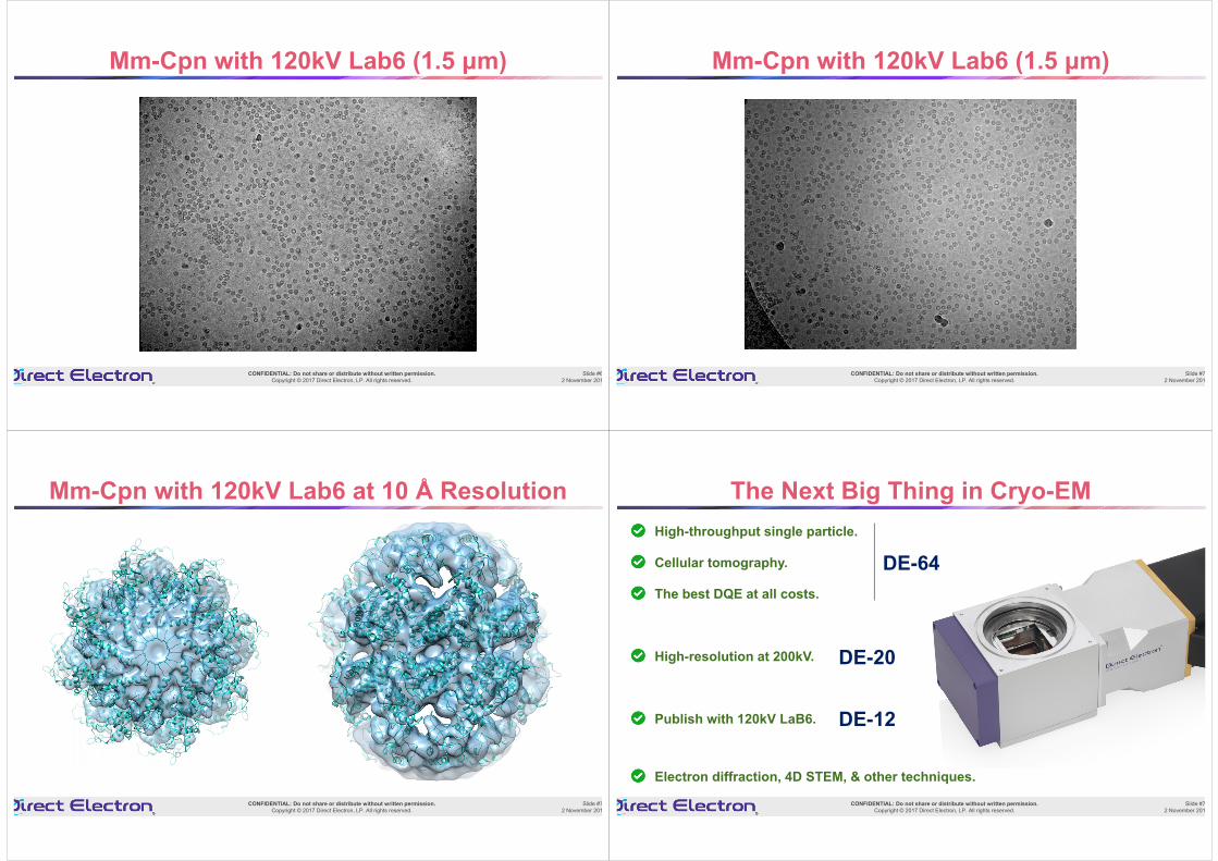
Mm-Cpn with 120kV Lab6 at 10 Å Resolution
CONFIDENTIAL: Do not share or distribute without written permission.Copyright © 2017 Direct Electron, LP. All rights reserved.
Slide #72 November 201
The Next Big Thing in Cryo-EMHigh-throughput single particle.
Cellular tomography. DE-64The best DQE at all costs.
High-resolution at 200kV.
Publish with 120kV LaB6.
DE-20
DE-12
Electron diffraction, 4D STEM, & other techniques.
CONFIDENTIAL: Do not share or distribute without written permission.Copyright © 2017 Direct Electron, LP. All rights reserved.
Slide #72 November 201
Cryo-ED of Catalase
~ 5 e-/Å2
CONFIDENTIAL: Do not share or distribute without written permission.Copyright © 2017 Direct Electron, LP. All rights reserved.
Slide #72 November 201
Cryo-ED of Catalase Movie (25 fps)
CONFIDENTIAL: Do not share or distribute without written permission.Copyright © 2017 Direct Electron, LP. All rights reserved.
Slide #72 November 201
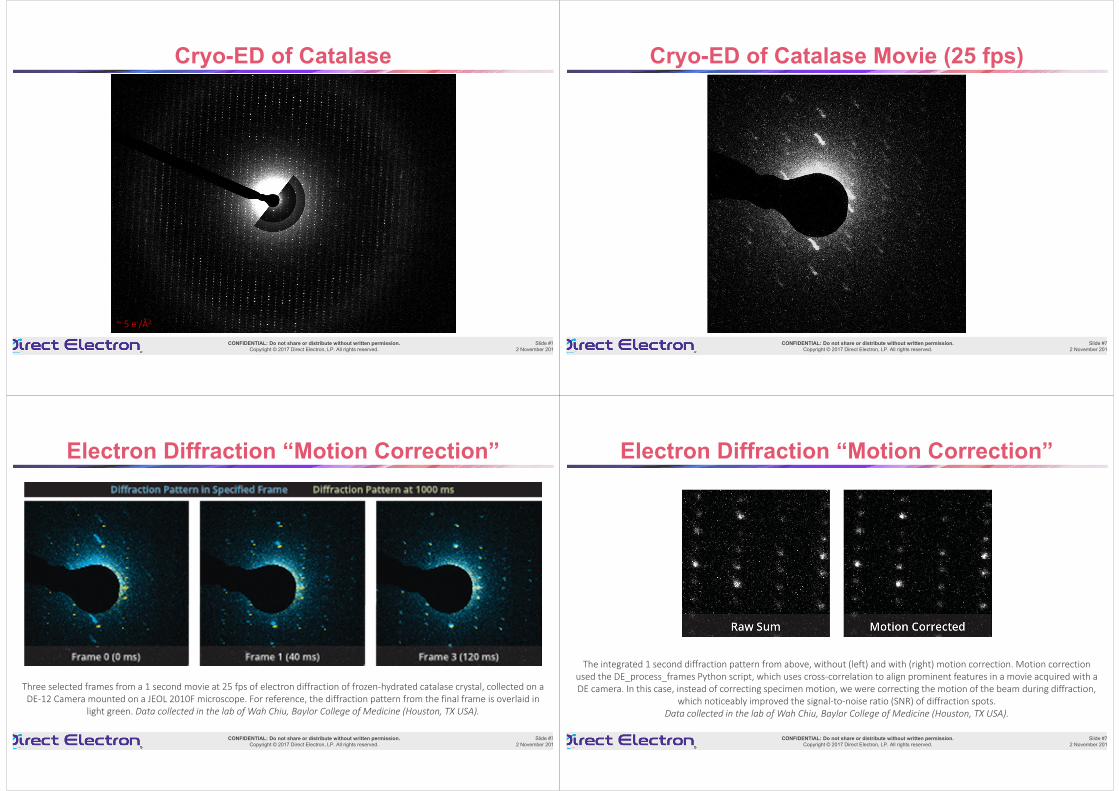
Electron Diffraction “Motion Correction”
Three selected frames from a 1 second movie at 25 fps of electron diffraction of frozen-hydrated catalase crystal, collected on a DE-12 Camera mounted on a JEOL 2010F microscope. For reference, the diffraction pattern from the final frame is overlaid in
light green. Data collected in the lab of Wah Chiu, Baylor College of Medicine (Houston, TX USA).
CONFIDENTIAL: Do not share or distribute without written permission.Copyright © 2017 Direct Electron, LP. All rights reserved.
Slide #72 November 201
Electron Diffraction “Motion Correction”
The integrated 1 second diffraction pattern from above, without (left) and with (right) motion correction. Motion correction used the DE_process_frames Python script, which uses cross-correlation to align prominent features in a movie acquired with a DE camera. In this case, instead of correcting specimen motion, we were correcting the motion of the beam during diffraction,
which noticeably improved the signal-to-noise ratio (SNR) of diffraction spots.Data collected in the lab of Wah Chiu, Baylor College of Medicine (Houston, TX USA).
CONFIDENTIAL: Do not share or distribute without written permission.Copyright © 2017 Direct Electron, LP. All rights reserved.
Slide #72 November 201
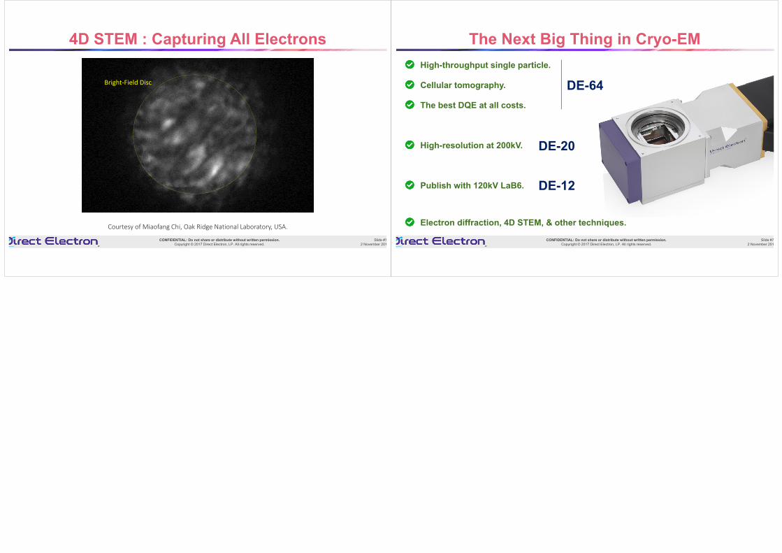
4D STEM : Capturing All Electrons
Courtesy of Miaofang Chi, Oak Ridge National Laboratory, USA.
Bright-Field Disc
CONFIDENTIAL: Do not share or distribute without written permission.Copyright © 2017 Direct Electron, LP. All rights reserved.
Slide #72 November 201
The Next Big Thing in Cryo-EMHigh-throughput single particle.
Cellular tomography. DE-64The best DQE at all costs.
High-resolution at 200kV.
Publish with 120kV LaB6.
DE-20
DE-12
Electron diffraction, 4D STEM, & other techniques.


