Embed Size (px)
Citation preview
PLEASE SCROLL DOWN FOR ARTICLE
This article was downloaded by: [Awasthi, Yogendra Kumar]On: 30 June 2009Access details: Access Details: [subscription number 912807146]Publisher Taylor & FrancisInforma Ltd Registered in England and Wales Registered Number: 1072954 Registered office: Mortimer House,37-41 Mortimer Street, London W1T 3JH, UK
International Journal of ElectronicsPublication details, including instructions for authors and subscription information:http://www.informaworld.com/smpp/title~content=t713599654
Equivalent isotropic relative permittivity of microstrip on multilayer anisotropicsubstrateA. K. Verma a; Y. K. Awasthi a; Himanshu Singh a
a Microwave Research Laboratory, Department of Electronic Science, University of Delhi, New Delhi, India
Online Publication Date: 01 August 2009
To cite this Article Verma, A. K., Awasthi, Y. K. and Singh, Himanshu(2009)'Equivalent isotropic relative permittivity of microstrip onmultilayer anisotropic substrate',International Journal of Electronics,96:8,865 — 875
To link to this Article: DOI: 10.1080/00207210902851480
URL: http://dx.doi.org/10.1080/00207210902851480
Full terms and conditions of use: http://www.informaworld.com/terms-and-conditions-of-access.pdf
This article may be used for research, teaching and private study purposes. Any substantial orsystematic reproduction, re-distribution, re-selling, loan or sub-licensing, systematic supply ordistribution in any form to anyone is expressly forbidden.
The publisher does not give any warranty express or implied or make any representation that the contentswill be complete or accurate or up to date. The accuracy of any instructions, formulae and drug dosesshould be independently verified with primary sources. The publisher shall not be liable for any loss,actions, claims, proceedings, demand or costs or damages whatsoever or howsoever caused arising directlyor indirectly in connection with or arising out of the use of this material.
Equivalent isotropic relative permittivity of microstrip on multilayer
anisotropic substrate
A.K. Verma, Y.K. Awasthi* and Himanshu Singh
Microwave Research Laboratory, Department of Electronic Science, University of Delhi,New Delhi 110021, India
(Received 20 November 2008; final version received 2 February 2009)
A closed-form model to obtain the equivalent isotropic relative permittivity of themultilayer microstrip line on the anisotropic substrate for 0 w/h � 10, anisotropicratio 0.5 � n � 3 for both low and high permittivity substrates is reported.The model has accuracy 0.5% against the full-wave method. It computes effectiverelative permittivity and characteristic impedance of microstrip on compositeanisotropic substrates with deviations 5.3% and 1.78%, respectively againstthe EM-software Empire. It is used to obtain dispersion in multilayer anisotropicsubstrate microstrip up to millimetre wave range with high accuracy against theresults of HFSS.
Keywords: anisotropic medium; characteristic impedance; equivalent effectivepermittivity; isotropic medium; microstrip transmission line
1. Introduction
The anisotropy in dielectric substrates affects the propagation parameters andcharacteristic impedance of a microstrip line. EM-simulators are available to take into account the anisotropy in a substrate. However, the closed-form expressions thatcould be incorporated in the Circuit-Simulators are not available. Such closed-formexpressions are also useful for the development of the CAD-oriented synthesisalgorithm needed for designing the planar circuits on anisotropic substrates. Theseclosed-form expressions are further useful to analyse distortion in the pulsespropagating on the anisotropic microstrip interconnects.
An effort has been made by several investigators to account for the effect ofanisotropy on the effective relative permittivity and characteristic impedance of amicrostrip line (Edwards and Owens 1976; Owens, Aitken and Edwards 1976;Alexopoulos and Krowne 1978; Alexopoulos 1985; Tsalamengas, Uzunoglu andAlexopoulos 1985; Hoffmann 1987; Fritsch and Wolff 1992). The closed-formexpressions are reported that convert the anisotropic substrate to the equivalentisotropic substrate with equivalent substrate thickness. However, these expressionsdo not consider the width/ height (w/h) ratio of an anisotropic microstrip line whileobtaining the equivalent isotropic relative permittivity (Owens et al. 1976;Alexopoulos 1985; Hoffmann 1987). As this popular method is not accurate,
*Corresponding author. Email: [email protected]
International Journal of Electronics
Vol. 96, No. 8, August 2009, 865–875
ISSN 0020-7217 print/ISSN 1362-3060 online
� 2009 Taylor & Francis
DOI: 10.1080/00207210902851480
http://www.informaworld.com
Downloaded By: [Awasthi, Yogendra Kumar] At: 06:09 30 June 2009
we must take into account the effect of w/h-ratio of the microstrip for accuratedetermination of the equivalent isotropic relative permittivity. Edward and Owens(1976) and Owens et al. (1976) have used the finite-difference method with ananalytical formula to achieve this end; whereas Fritsch and Wolff (1992) have usedthe full-wave method. Edward and Owens (1976) have also given a closed-formexpression to get an equivalent isotropic relative permittivity. However, it isapplicable only to the Sapphire substrate (Edwards and Owens 1976). Theseresearchers have not considered microstrip on multilayer anisotropic substrates.
The present work reports the w/h-ratio dependent closed-form model to computethe equivalent isotropic relative permittivity of the anisotropic microstrip linewithout using the finite difference or the full-wave method. The model is valid over awide range of line parameters. The accuracy of the model is tested against theavailable experimental and numerical results and also against the results obtainedfrom the EM-software Empire (IMST-Empire v-4.20, GmbH, Germany). The modelis further extended to microstrips on multilayer anisotropic substrates.
2. The model
The process of getting the w/h dependent equivalent isotropic relative permittivity(ew=hreq;iso) of the anisotropic substrate is shown in Figure 1. It involves two steps. (i) To getthe equivalent isotropic substrate with isotropic relative permittivity (er,eq) and the equi-valent substrate thickness (heq) without consideration of the w/h-ratio. (ii) To get the w/hdependent equivalent isotropic relative permittivity ew=hreq;iso with the original substratethickness (h). We have used the method of partial capacitance to develop the model.
Step no. 1: The following standard relations convert the anisotropic substrate of amicrostrip to an equivalent isotropic substrate er,ew and equivalent substrate thicknessheq without accounting for the affect of w/h ratio (Alexopoulos 1985; Hoffmann 1987)
er;eq ¼ffiffiffiffiffiffiffiffiffiffiffiffiffiffiffiffiffiffiffiffiffiffiffiffiffiffiffiffiffiffiffiffiffierxxeryy � ðerxyÞ2
q; heq ¼ h
ffiffiffiffiffiffiffiffiffiffiffiffiffiffiffiffiffiffiffiffiffiffiffiffiffiffiffiffiffiffiffiffiffiffiffierxxeryy� erxy
eryy
� �2" #vuut ð1Þ
where,
erxx ¼ er&cos2yþ erZsin2y; eryy ¼ er&sin
2yþ erZcos2y
erxy ¼ eryx ¼ ðer& � erZÞsin y cos y;
er& ¼ er?; erZ ¼ erjj; Anisotropic ratio n ¼ffiffiffiffiffiffiffierxxeryy
rð2Þ
Figure 1. Process of obtaining w/h dependent equivalent isotropic substrate�ew=hreq;iso
�:
866 A.K. Verma et al.
Downloaded By: [Awasthi, Yogendra Kumar] At: 06:09 30 June 2009
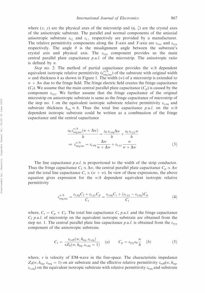
where (x, y) are the physical axes of the microstrip and (Z, z) are the crystal axesof the anisotropic substrate. The parallel and normal components of the uniaxialanisotropic substrate erjj and er? respectively are provided by a manufacturer.The relative permittivity components along the X-axis and Y-axis are erxx and eryyrespectively. The angle y is the misalignment angle between the substrate’scrystal axis and physical axis. The eryy component provides us the maincentral parallel plate capacitance p.u.l. of the microstrip. The anisotropic ratiois defined by n.
Step no. 2: The method of partial capacitance provides the w/h dependentequivalent isotropic relative permittivity (ew=hreq;iso) of the substrate with original widthw and thickness h as shown in Figure 1. The width (w) of a microstrip is extended tow þ Dw due to the fringe field. The fringe electric field creates the fringe capacitance(Cf). We assume that the main central parallel plate capacitance (Cp) is caused by thecomponent eryy. We further assume that the fringe capacitance of the originalmicrostrip on anisotropic substrate is same as the fringe capacitance of microstrip ofthe step no. 1 on the equivalent isotropic substrate relative permittivity er,eq andsubstrate thickness heq � h. Thus the total line capacitance p.u.l. on the w/hdependent isotropic substrate could be written as a combination of the fringecapacitance and the central capacitance
e0 ew=hreq;isoðwþ DwÞ
h¼ e0 er;eqDw
hþ e0 er;yyw
h
) ew=hreq;iso ¼ er;eqDw
wþ Dwþ er;yy
w
wþ Dwð3Þ
The line capacitance p.u.l. is proportional to the width of the strip conductor.Thus the fringe capacitance Cf / Dw, the central parallel plate capacitance Cp / Dwand the total line capacitance Ct / (w þ w). In view of these expressions, the aboveequation gives expression for the w/h dependent equivalent isotropic relativepermittivity
ew=hreq;iso ¼er;eqCf þ er;yyCp
Ct¼ er;eqCt þ ðer;yy � er;eqÞCp
Ctð4Þ
where, Ct ¼ Cp þ Cf. The total line capacitance Ct p.u.l. and the fringe capacitanceCf p.u.l. of microstrip on the equivalent isotropic substrate are obtained from thestep no. 1. The central parallel plate line capacitance p.u.l. is obtained from the eryycomponent of the anisotropic substrate.
Ct ¼er effðw; heq; er;eqÞ
vZ0ðw; heq; er;eq ¼ 1Þ ðaÞ Cp ¼ eryye0w
hðbÞ ð5Þ
where, v is velocity of EM-wave in the free-space. The characteristic impedanceZ0(w, heq, ereq ¼ 1) on air substrate and the effective relative permittivity ereff(w, heq,er,eq) on the equivalent isotropic substrate with relative permittivity ereq and substrate
International Journal of Electronics 867
Downloaded By: [Awasthi, Yogendra Kumar] At: 06:09 30 June 2009
thickness heq are obtained from the closed-form expression of Hammerstad-Jensen(Hammerstad and Jensen 1980).
We can use the w/h dependent equivalent isotropic relative permittivity ew=hreq;iso
with substrate thickness h and strip width w to compute the correct static effectiverelative permittivity and characteristic impedance of the original microstrip on theanisotropic substrate by using again the closed-form expression of Hammerstad-Jensen (Hammerstad and Jensen 1980). Any dispersion model can be used on thesubstrate with ew=hreq;iso to get the frequency dependent effective relative permittivityand characteristic impedance of the anisotropic substrate microstrip (Krischniningand Jansen 1982; Hoffmann 1987).
3. Validation of model
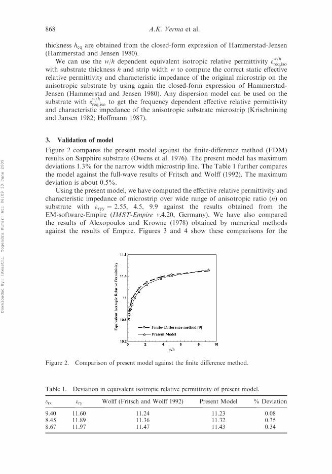
Figure 2 compares the present model against the finite-difference method (FDM)results on Sapphire substrate (Owens et al. 1976). The present model has maximumdeviations 1.3% for the narrow width microstrip line. The Table 1 further comparesthe model against the full-wave results of Fritsch and Wolff (1992). The maximumdeviation is about 0.5%.
Using the present model, we have computed the effective relative permittivity andcharacteristic impedance of microstrip over wide range of anisotropic ratio (n) onsubstrate with eryy ¼ 2.55, 4.5, 9.9 against the results obtained from theEM-software-Empire (IMST-Empire v.4.20, Germany). We have also comparedthe results of Alexopoulos and Krowne (1978) obtained by numerical methodsagainst the results of Empire. Figures 3 and 4 show these comparisons for the
Table 1. Deviation in equivalent isotropic relative permittivity of present model.
erx ery Wolff (Fritsch and Wolff 1992) Present Model % Deviation
9.40 11.60 11.24 11.23 0.088.45 11.89 11.36 11.32 0.358.67 11.97 11.47 11.43 0.34
Figure 2. Comparison of present model against the finite difference method.
868 A.K. Verma et al.
Downloaded By: [Awasthi, Yogendra Kumar] At: 06:09 30 June 2009
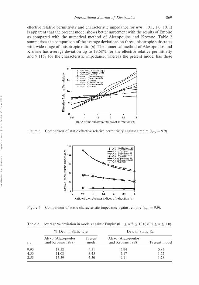
effective relative permittivity and characteristic impedance for w/h ¼ 0.1, 1.0, 10. Itis apparent that the present model shows better agreement with the results of Empireas compared with the numerical method of Alexopoulos and Krowne. Table 2summarises the comparison of the average deviations on three anisotropic substrateswith wide range of anisotropic ratio (n). The numerical method of Alexopoulos andKrowne has average deviation up to 13.58% for the effective relative permittivityand 9.11% for the characteristic impedance; whereas the present model has these
Table 2. Average % deviation in models against Empire (0.1 � w/h � 10.0) (0.5 � n � 3.0).
% Dev. in Static er,eff Dev. in Static Z0
eryAlexo (Alexopoulosand Krowne 1978)
Presentmodel
Alexo (Alexopoulosand Krowne 1978) Present model
9.90 13.58 4.51 5.94 0.854.50 11.08 3.45 7.17 1.522.55 13.59 5.30 9.11 1.78
Figure 3. Comparison of static effective relative permittivity against Empire (eryy ¼ 9.9).
Figure 4. Comparison of static characteristic impedance against empire (eryy ¼ 9.9).
International Journal of Electronics 869
Downloaded By: [Awasthi, Yogendra Kumar] At: 06:09 30 June 2009
deviations at only 5.3% and 1.78%. We note that the computed results of effectiverelative permittivity by several EM-software also have large variations amongthemselves. Table 3 shows percent deviation in computed results of the effectiverelative permittivity obtained by Empire and HFSS against the results of Sonnet(Sonnet-Lite v11.55, Syracuse, NY, USA). The maximum deviation in Empire andHFSS are 10.9% and 7.08% respectively. Empire has maximum deviation for thenarrow, line, whereas HFSS has maximum deviation for the wide line. The averagedeviation for the Empire and HFSS are 5% and 4% respectively with respect toSonnet. In view of these comparisons, the present model appears to be accurate andacceptable for design work.
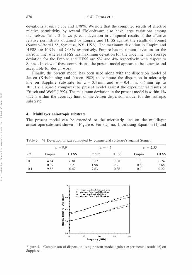
Finally, the present model has been used along with the dispersion model ofJensen (Krischnining and Jansen 1982) to compute the dispersion in microstripline on Sapphire substrate for h ¼ 0.4 mm and w ¼ 0.4 mm, 0.6 mm up to30 GHz. Figure 5 compares the present model against the experimental results ofFritsch and Wolff (1992). The maximum deviation in the present model is within 1%that is within the accuracy limit of the Jensen dispersion model for the isotropicsubstrate.
4. Multilayer anisotropic substrate
The present model can be extended to the microstrip line on the multilayeranisotropic substrate shown in Figure 6. For step no. 1, on using Equation (1) and
Table 3. % Deviation in ereff computed by commercial software’s against Sonnet.
er ¼ 9.9 er ¼ 4.5 er ¼ 2.55
w/h Empire HFSS Empire HFSS Empire HFSS
10 4.64 6.81 3.12 7.08 1.8 6.241 0.99 5.2 1.98 2.9 0.86 2.680.1 9.88 0.47 7.63 0.36 10.9 0.22
Figure 5. Comparison of dispersion using present model against experimental results [6] onSapphire.
870 A.K. Verma et al.
Downloaded By: [Awasthi, Yogendra Kumar] At: 06:09 30 June 2009
Equation (2), we convert each anisotropic layer of thickness hm (m ¼ 1, 2 . . . N) withrelative permittivity (erm.xx, erm,yy) to the equivalent relative permittivity erm,eq
(m ¼ 1, 2 . . . N) and equivalent substrate thickness heq,m (m ¼ 1, 2 . . . N). Step no. 2provides the w/h dependent equivalent isotropic relative permittivity ew=Hreq;iso for singlelayer substrate of thickness H ¼ h1 þ h2 þ . . . þ hN.
We convert the multilayer anisotropic substrate to an equivalent single layerisotropic substrate er,eq by using the single layer reduction (SLR) formulation(Verma and Hassani Sadr 1992). First, we convert each anisotropic layer to theequivalent isotropic layer mentioned above. Next, we compute the effective relativepermittivity er,eff(w/Heq, eri,eq) of the multilayer microstrip line on the equivalentisotropic substrate by using the variational method with TTL technique (Yamashita1968; Crampagne, Ahmadpanah and Guiraud 1978). Thus the effective relativepermittivity of the multilayer anisotropic substrate is
er;effðw=Heq; eri;eqÞ ¼C ðw; heq1; . . . heqN; eri;eq1; . . . eri;eqNÞC0 ðw; H; eri;eq1 ¼ . . . :eri;eqN ¼ 1Þ ð6Þ
where layer wise equivalent isotropic relative permittivity eri,eqm (m ¼ 1, 2 . . . N) andequivalent substrate thickness heqm (m ¼ 1, 2 . . . N) for each layer are obtained fromEquation (1). The line capacitance p.u.l. of the microstrip line on the multilayersubstrate is obtained by the variational method (Yamashita 1968; Crampagne et al.1978; Verma and Hassani Sadr 1992)
1
C ðw; heq1;heq2; . . . heqN; eri;eq1; eri;eq2 . . . eri;eqNÞ¼ 1
p e0
Z10
~fðbÞ=Qh i2
Y bdb ð7Þ
The line capacitance on the air substrate C0(w,H, eri,eq1 ¼ . . . eri,eqN ¼ 1) is alsoobtained from the above expression. Y is the admittance function of the TTLmethod signifying Green’s function, ~f (b) is the assumed trial charge distributionfunction in Fourier domain and Q is the total charge on microstrip line for the trialcharge distribution.
In the SLR formulation, the multilayer microstrip line is reduced to anequivalent single layer substrate of thickness H (¼h1 þ h2 þ . . . þ hN) andequivalent isotropic relative permittivity er,eq(w/Heq, eri,eq). The equivalent isotropic
Figure 6. Multilayer anisotropic substrate microstrip line.
International Journal of Electronics 871
Downloaded By: [Awasthi, Yogendra Kumar] At: 06:09 30 June 2009
relative permittivity is obtained from the Wheeler’s transformation (Verma andHassani Sadr 1992)
er;eqðw=Heq; eri;eqÞ ¼ 1þ er;effðw=Heq; eri;eqÞ � 1
qðw=HÞ ð8Þ
where, Heq ¼ h1eq þ h2eq þ . . . þ hNeq and the filling-factor q(w/H) is obtainedfrom
q ¼ 1
2ð1þ pÞ; p ¼
1þ 12Hw
h i�1=2wH � 1
1þ 12Hw
h i�1=2þ 0:04 1� w
H
h i2; w
H < 1
8><>: ð9Þ
The total line capacitance of the multilayer microstrip line is computed from
Ct ¼er;effðw=Heq; eri;eqÞ
v Z0ðw=H; e�r1 ¼ . . . e�rN ¼ 1Þ ð10Þ
where, v is the velocity of EM-wave in the free-space. The characteristic impedanceof microstrip on air-substrate, Z0ðw=H; e�r1 ¼ . . . e�rN ¼ 1Þ is obtained from theclosed-form expression of Hammerstad and Jensen (1980). The central capacitanceof the multilayer anisotropic substrate microstrip is obtained from the yy-componentof the anisotropic relative permittivity
Cp ¼eo eryy; eq w
HðaÞ eryy; eq ¼
HPNi
hieryy; i
h i ðbÞ ð11Þ
Finally the w/H dependent equivalent single layer isotropic substrate of relativepermittivity ew=Hreq;iso and thickness H is obtained from Equation (4) in which substrateer,eq is taken from Equation (8), er,yy is replaced by eryy,eq from Equation (11b), Ct
and Cp are taken from Equations (10) and (11a) respectively. The variational methodor Hammerstad-Jensen formula (Hammerstad and Jensen 1980) is applied on thisequivalent isotropic substrate to obtain the effective relative permittivity eanisoreff of themultilayer anisotropic microstrip line. The static characteristic impedance Zaniso
O ofthe multilayer anisotropic microstrip line can also be computed on this equivalentisotropic substrate by using the Hammerstad-Jensen expression. The unifieddispersion model (Verma and Hassani Sadr 1992) can be used to compute thedispersion in the multilayer anisotropic microstrip line.
5. Results of multilayer anisotropic substrate microstrip line
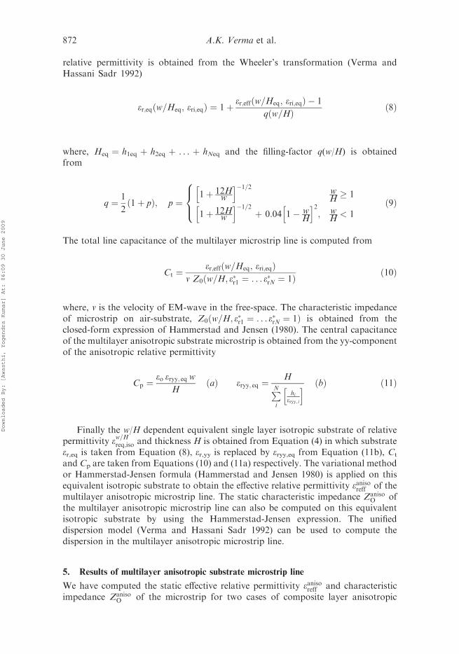
We have computed the static effective relative permittivity eanisoreff and characteristicimpedance Zaniso
O of the microstrip for two cases of composite layer anisotropic
872 A.K. Verma et al.
Downloaded By: [Awasthi, Yogendra Kumar] At: 06:09 30 June 2009
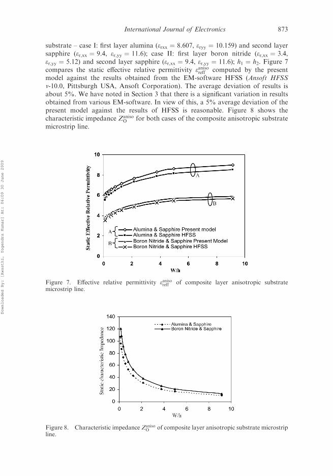
substrate – case I: first layer alumina (erxx ¼ 8.607, eryy ¼ 10.159) and second layersapphire (er,xx ¼ 9.4, er,yy ¼ 11.6); case II: first layer boron nitride (er,xx ¼ 3.4,er,yy ¼ 5.12) and second layer sapphire (er,xx ¼ 9.4, er,yy ¼ 11.6); h1 ¼ h2. Figure 7compares the static effective relative permittivity eanisoreff computed by the presentmodel against the results obtained from the EM-software HFSS (Ansoft HFSSv-10.0, Pittsburgh USA, Ansoft Corporation). The average deviation of results isabout 5%. We have noted in Section 3 that there is a significant variation in resultsobtained from various EM-software. In view of this, a 5% average deviation of thepresent model against the results of HFSS is reasonable. Figure 8 shows thecharacteristic impedance Zaniso
O for both cases of the composite anisotropic substratemicrostrip line.
Figure 7. Effective relative permittivity eanisoreff of composite layer anisotropic substratemicrostrip line.
Figure 8. Characteristic impedance ZanisoO of composite layer anisotropic substrate microstrip
line.
International Journal of Electronics 873
Downloaded By: [Awasthi, Yogendra Kumar] At: 06:09 30 June 2009
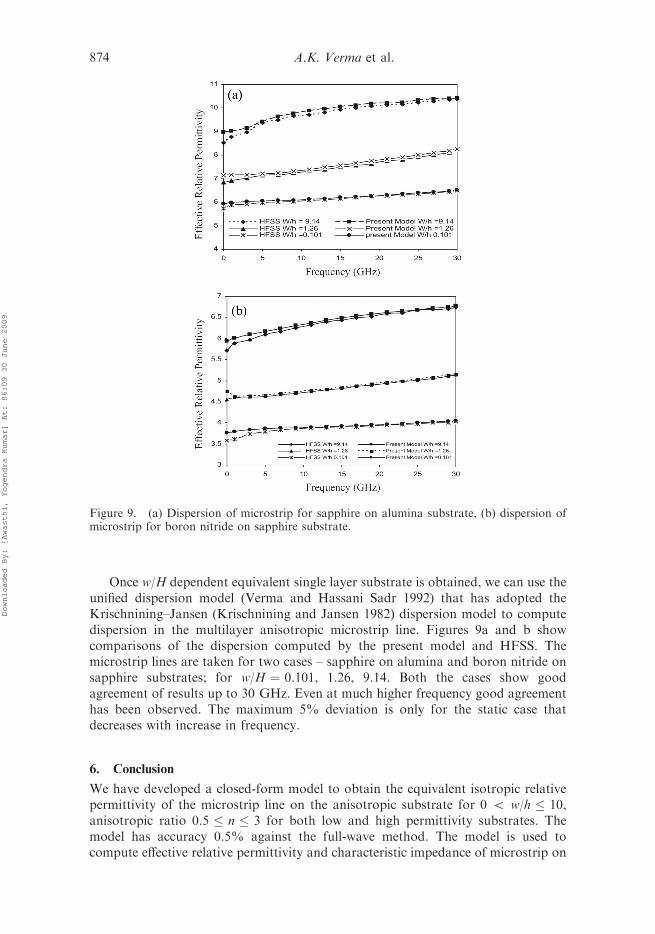
Once w/H dependent equivalent single layer substrate is obtained, we can use theunified dispersion model (Verma and Hassani Sadr 1992) that has adopted theKrischnining–Jansen (Krischnining and Jansen 1982) dispersion model to computedispersion in the multilayer anisotropic microstrip line. Figures 9a and b showcomparisons of the dispersion computed by the present model and HFSS. Themicrostrip lines are taken for two cases – sapphire on alumina and boron nitride onsapphire substrates; for w/H ¼ 0.101, 1.26, 9.14. Both the cases show goodagreement of results up to 30 GHz. Even at much higher frequency good agreementhas been observed. The maximum 5% deviation is only for the static case thatdecreases with increase in frequency.
6. Conclusion
We have developed a closed-form model to obtain the equivalent isotropic relativepermittivity of the microstrip line on the anisotropic substrate for 0 5 w/h � 10,anisotropic ratio 0.5 � n � 3 for both low and high permittivity substrates. Themodel has accuracy 0.5% against the full-wave method. The model is used tocompute effective relative permittivity and characteristic impedance of microstrip on
Figure 9. (a) Dispersion of microstrip for sapphire on alumina substrate, (b) dispersion ofmicrostrip for boron nitride on sapphire substrate.
874 A.K. Verma et al.
Downloaded By: [Awasthi, Yogendra Kumar] At: 06:09 30 June 2009
anisotropic substrate with deviations 5.3% and 1.78% respectively against theEM-software Empire; whereas the numerical method of Alexopoulos and Krownehas average deviation up to 13.58% for the effective relative permittivity and 9.11%for the characteristic impedance. The model is extended to the multilayer anisotropicsubstrate microstrip line with deviation 5%. The model computes dispersion inmultilayer anisotropic substrate microstrip with good accuracy. The model is usefulfor the development of accurate synthesis programs for the single layer andmultilayer anisotropic microstrip lines needed for the design of circuits andcomponents. The model can also be used for analysing the effect of anisotropy onthe pulse propagation on the multilayer anisotropic microstrip line.
References
Alexopoulos, N.G. (1985), ‘Integrated-Circuit Structures on Anisotropic Substrates’, IEEETransactions on Microwave Theory and Techniques, MTT- 33, 847–881.
Alexopoulos, N.G., and Krowne, C.M. (1978), ‘Characteristics of Single and CoupledMicrostrips on Anisotropic Substrates’, IEEE Transactions on Microwave Theory andTechniques, MTT-26, 387–393.
Crampagne, R., Ahmadpanah, M., and Guiraud, J.L. (1978), ‘A Simple Method forDetermining the Green’s Function for a Large Class of MIC Lines having multilayeredDielectric Structures’, IEEE Transactions on Microwave Theory and Techniques, MTT-26,82–87.
Edwards, T.C., and Owens, R.P. (1976), ‘2–18-GHz Dispersion Measurements on 10–100-OMicrostrip lines on Sapphire’, IEEE-MTT, 24, 506–513.
Fritsch, U., and Wolff, I. (1992), ‘Characterization of Anisotropic Substrate Materials forMicrowave Applications’, IEEE.MTT-S, 1131–1134.
Hammerstad, E., and Jensen, O. (1980), ‘Accurate models for Microstrip Computer AidedDesign’, IEEE MTT-S. International Microwave Symposium Digest, 407–409.
Hoffmann, R.K. (1987), Handbook of Microwave Integrated Circuits, USA: Artech House,Chapter-8, pp. 213–224.
Krischnining, M., and Jansen, R.H. (1982), ‘Accurate model for effective dielectric constantwith validity up to millimetre-wave frequency’, Electronics Letters, 18, 272–273.
Owens, R.P., Aitken, J.E., and Edwards, T.C. (1976), ‘Quasi-Static Characteristics ofMicrostrip on an Anisotropic Sapphire substrate’, IEEE Transaction on MTT, 24, 499–505.
Tsalamengas, J.L., Uzunoglu, N.K., and Alexopoulos, N.G. (1985), ‘Propagation Character-istics of a Microstrip Line Printed on a General Anisotropic Substrate’, IEEE Transactionson Microwave Theory and Techniques, MTT-33, 941–945.
Verma, A.K., and Hassani Sadr, G. (1992), ‘Unified Dispersion Model for MultilayerMicrostrip Line’, IEEE Transactions on Microwave Theory and Techniques, 40, 1587–1591.
Yamashita, E. (1968), ‘Variational Method for the Analysis of Microstrip like TransmissionLines’, IEEE Transactions on Microwave Theory and Techniques, MTT-16, 529–535.
International Journal of Electronics 875
Downloaded By: [Awasthi, Yogendra Kumar] At: 06:09 30 June 2009


