Embed Size (px)
Citation preview
INDIAN JOURNAL OF SCIENCE AND TECHNOLOGY
RESEARCH ARTICLE
OPEN ACCESS
Received: 15.10.2020Accepted: 12.12.2020Published: 11.01.2021
Citation: Raval V, Patel A (2021)Narrowband aperture coupledwaveguide to microstrip transitionfor space applications. IndianJournal of Science and Technology14(1): 33-45. https://doi.org/10.17485/IJST/v13i1.1848∗Corresponding author.
Tel: [email protected]
Funding: None
Competing Interests: None
Copyright: © 2021 Raval & Patel.This is an open access articledistributed under the terms of theCreative Commons AttributionLicense, which permits unrestricteduse, distribution, and reproductionin any medium, provided theoriginal author and source arecredited.
Published By Indian Society forEducation and Environment (iSee)
ISSNPrint: 0974-6846Electronic: 0974-5645
Narrowband aperture coupled waveguideto microstrip transition for spaceapplications
Vidhi Raval1∗, Amit Patel2
1 PhD Scholar, Charusat University, CSPIT, Changa, Anand, 388421, Gujarat, India. Tel.: +091-7452552292 Assistant Professor, Charusat University, CSPIT, Changa, Anand, 388421, Gujarat, India
AbstractBackground/Objectives: To design, analyze and fabricate aperture coupledwaveguide to microstrip transition for Ka-Band where energy is coupledthrough slot in ground plane and a metal patch placed over the substrate.Methods: Impedance matching approach has been adopted for transitiondesign. Microstrip line is inserted into the waveguide through aperture actingas a probe. Followed by inductive line and transformer line for impedancetranslation between waveguide and microstrip line. Waveguide transitionhas been designed using Ansoft High Frequency Structure Simulator (HFSS)full-wave EM simulator. Findings: Designed transition shows return lossperformance better than 15 dB and insertion loss better than 0.5 dB forback to back configuration over a frequency band of 34 – 36 GHz. Transitionis fabricated on RT5580 Duroid substrate (∈r= 2.2) with substrate thickness0.254 mm. Measured results show return loss better than 25 dB and insertionloss less than 1 dB over a frequency band of 34-36 GHz. Table 2 showscomparison of present design with previously reported designs in terms ofperformance. Novelty/Applications: Comparison of the presented transitionshows superior performance to previously reported transition designs in termsof transition bandwidth and insertion loss. Aperture coupled transitions canbe widely used for space applications where hermetic sealing is requiredand it saves extra effort for sealing. Certain RF circuit applications requirenarrowband waveguide transitions to attain required performance, in this caseaperture coupled transition can be a good option and its integration with RFcircuits is also easy. Fabricated transition design results show good agreementwith simulated results so it can be concluded that design is tolerant tofabrication errors. Transition has been fabricated using standard PCB processso production of such transition can be done easily without requirement of anyspecial facility for fabrication.Keywords: Aperture coupled transition; waveguide; microstrip; kaBand;hermetically sealed
https://www.indjst.org/ 33
Raval & Patel / Indian Journal of Science and Technology 2021;14(1):33–45
1 IntroductionIn past few decades, millimeter wave frequencies have been major attraction to lot of researchers due variety of applicationsin various fields like detection of objects (1), remote sensing (2) and astronomy (3). At millimeter and sub-millimeter wavefrequencies waveguides are often used as interconnect to RF subsystems like Low Noise Amplifiers (LNA), filters, mixers, etc.,as it offers low propagation losses and high-power handling capability. Thus, Waveguide to microstrip transitions have becomea major component in millimeter wave systems. Waveguide transitions can be realized using two concepts either by impedancematching or by mode conversion techniques. Inline and Ridge waveguide transition are realized using mode conversiontechniques. Aperture coupled and transversal transitions are implemented by applying impedance matching technique.
Choice of waveguide transition technique for implementation depends on the type of applications. Ridge waveguidetransitions can be used in applications where low propagation loss is intended. On other hand applications where size isa constraint inline transitions can be better option. Transversal transitions can be used in broadband applications whereasaperture coupled transition can be used where narrow band operation is required
Simple transition from microstrip to waveguide using aperture coupled patch was introduced in 1992 (4). Proximity feedingtechnique is employed for energy coupling between microstrip lines via slot in ground plane to metal patch element placed onan additional substrate. However, experimental results show narrowband performance due to smaller patch length. Aperturecoupled transition design does not require back short so application where space is constraint and waveguide is required atbackplane of circuit such transition can be used for implementation. Aperture coupled transition offer remarkable advantagein space constraint applications, as it does not require back short.
Transition design for W band frequencies has been presented (5) where increase in bandwidth is achieved by moving patchelement intowaveguidewall resulting increase in distance from feed point.Whereas drawback of this design it added complexityin fabrication and assembly of transition. Based on the experimental results of design presented in (6) shows the presence of EM(Electromagnetic) radiation on top of circuit which in turn reduces coupling of energy between microstrip line and waveguide.This is the major drawback of aperture coupled waveguide transition which occurs due to bidirectional nature of radiationpropagating from slot aperture. Back radiations can be reduced by using slot in ground plane of microstrip in order to coupleenergy between microstrip line and waveguide as presented in (7). In this design an additional second substrate with certainthickness covers aperture inside the waveguide and it works as quarter wave transformer for matching impedance betweenwaveguide and microstrip line. Experimental results presented in this paper show reduction in back side radiations. Anotherapproach presented in (8) to reduce back side radiation is using CPW (Coplanar Waveguide) instead of microstrip line. Fromexperimental results it can be seen that reduction in backside radiation occurs by aligning of feed structure, but the drawbackof such design is reduction in pass band and frequency shift.
Designing of rectangularwaveguide transition at higher frequency,mechanical tolerances becomes an issue. In such scenario,transition should consist of minimum parts and preferably a single substrate in order to make transition design more robustagainst fabrication and assembly tolerances. Design presented in (9) provides solution to few of these aspects by analyzingcoupling mechanism between patch element and microstrip line. Similar approach has been presented in this present articlewhere coupling mechanism has been exploited using cavity model for patch antenna using matching element. Simulations havebeen carried out to optimize the patch element length that controls generation of higher modes.
Another technique (10) where one side of substrate cover the cross section of waveguide and other side of substrate slot hasbeen defined, coupling between waveguide and microstrip line is employed using quarter wave transformer as a matchingelement.
This structure offers benefits of easy fabrication and hermiticity. However, the design measurement results show resonatingmode. One of the reasons was alumina substrate with high dielectric constant causes resonance. Thus, the transition designpresented in this article is designed using duroid substrate that has a lower dielectric constant.
Sensitivity analysis on manufacturing tolerance is presented in (11). Results show that radiating slots and misalignment withwaveguide center line are reason for reduction in energy coupling and errors in quarter wave transformer line causes impedancemismatch. Based on this study, simulations were carried out for optimizing various parameters affecting the performance ofthe transition that has been discussed in section 4 of this article.
An improved version of slot coupling was presented in (12), where a half wave transformer resonant slot aperture couplesenergy between waveguide and microstrip by shielding with periodic structure to suppress backside radiation from slot inoffer to avoid coupling of parallel modes by cap packaging. Design shows improved performance but increases manufacturingcomplexity.
Article presented in (13) shows inline microstrip to waveguide transition based on chebyshev transformer implemented ingap waveguide technology. But the issue with the design is fabrication errors can cause propagation of higher modes. SIW tomicrostrip transition is presented using LTCC technology (14) in which broadband response has been achieved using matching
https://www.indjst.org/ 34
Raval & Patel / Indian Journal of Science and Technology 2021;14(1):33–45
element. But experimental results showhigher radiationwhich causes low energy couplingwhich in turn causes higher insertionloss.
Gap waveguide-based design has been presented (15) to eliminate higher modes by using bed of nails. Drawback of suchdesign is waveguide height lower than 0.6 mm can only be used otherwise second order modes propagation may occur. Toaddress this issue design has been modified by adding ridge to suppress higher order modes. Design presented in (16) showstransversal transition design for sub-millimeter frequencies where higher mode suppression along microstrip line has beendone by designing structure for shielding. Design presented is simple and easy to fabricate. Aperture coupled transition hasbeen presented in (17). High coupling has been achieved using quarter wave transformer line from center of aperture. However,the drawback of this design is size of aperture needs to be very small in order to avoid the coupling of higher modes betweenSIW and microstrip line. Transversal transition with new impedance transformer structure has been proposed in (18). Higherflexibility in matching is offered due to transformer element but drawback of design is that performance highly depends onfabrication tolerances.
Based on the above study transition design presented in this letter addresses major drawbacks of aperture coupled transitionthose are backside radiation and higher modes propagation. Therefore, transition is designed using a matching element andquarter wave transformer line which is used as matching impedance between waveguide and microstrip line. Moreover, thetransition structure is simple and compatible with conventional low-cost PCB process. For demonstration of this work aprototype of back-to-back waveguide transition is implemented andmeasured.Themeasurement results show good agreementwith simulated results.
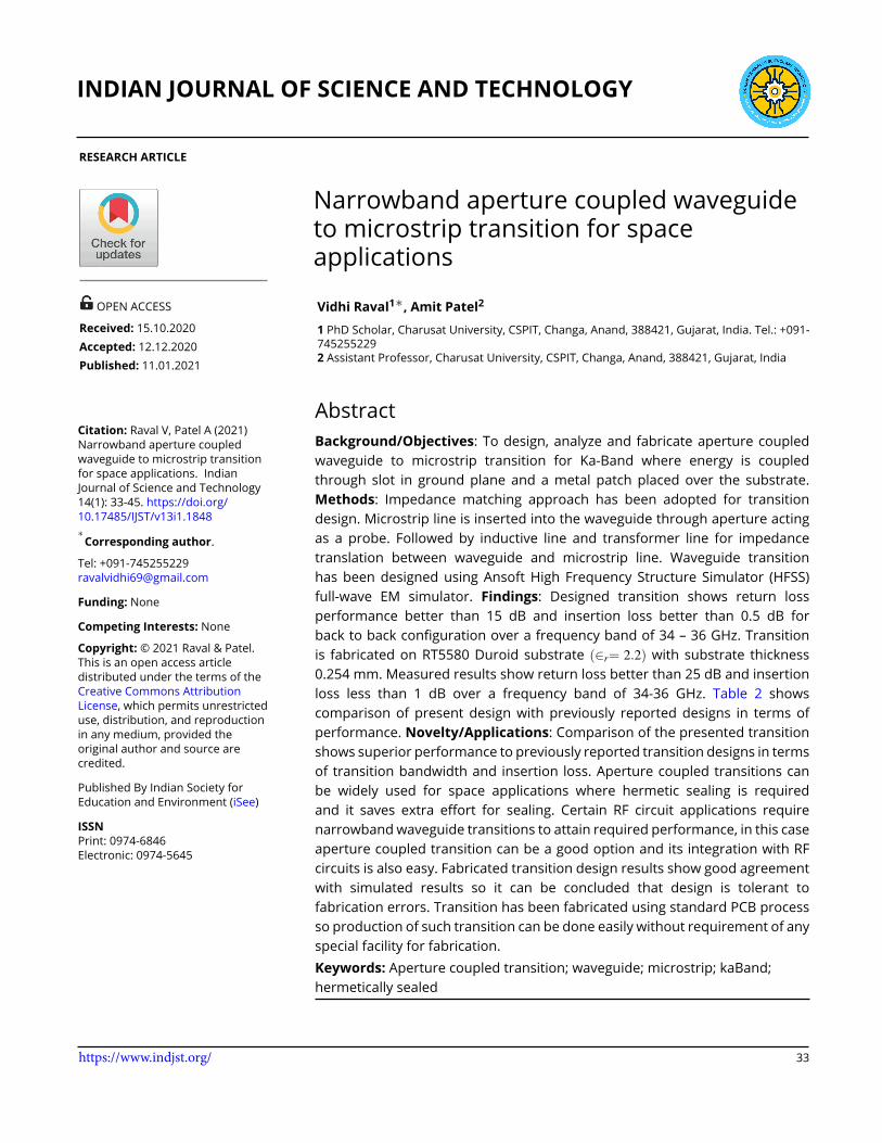
2 Design and numerical investigationDesign presented in this paper is a proximity coupled waveguide transition. Entire transition has been designed on a singlesubstrate and substrate is attached to waveguide. Such waveguide transitions are easy to fabricate and assemble. The conductorpattern consists of a patch onbottom layer of the transition andprobe at the upper side of dielectric substrate.Dielectric substrateused for design is RT5880 with dielectric constant 2.2 and loss tangent of 1E-04. Substrate thickness 0.254 mm. Rectangularpatch on the lower side is surrounded by grounding vias. Aperture is surrounded by grounding via to connect surroundingground and waveguide short electrically.
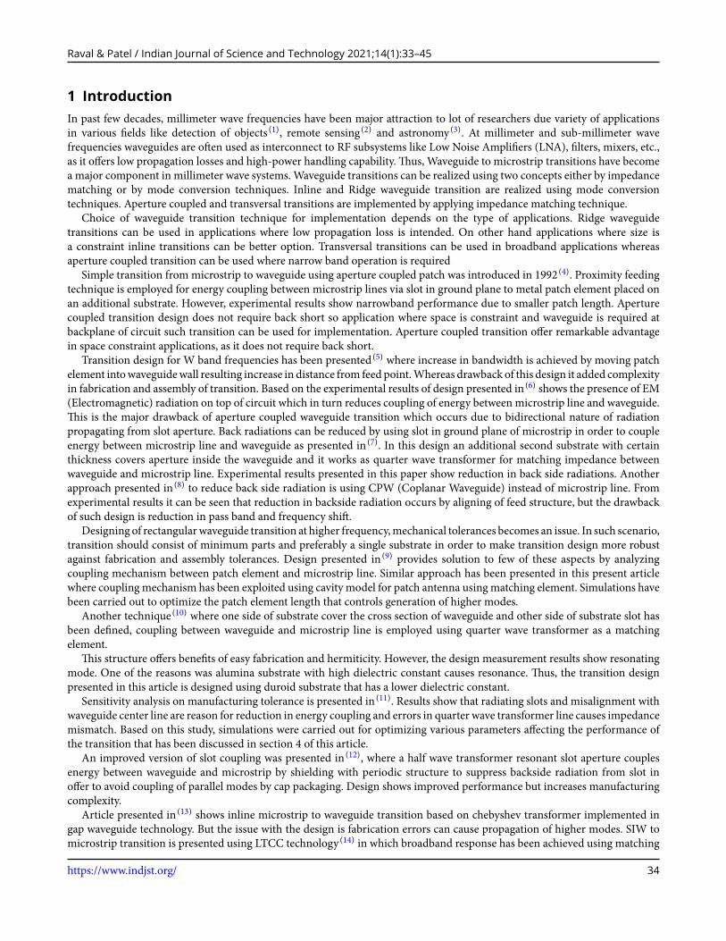
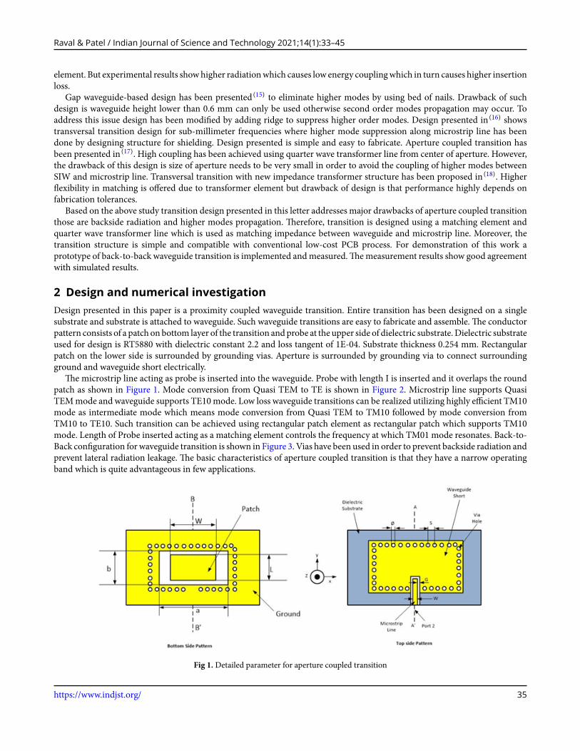
The microstrip line acting as probe is inserted into the waveguide. Probe with length I is inserted and it overlaps the roundpatch as shown in Figure 1. Mode conversion from Quasi TEM to TE is shown in Figure 2. Microstrip line supports QuasiTEMmode and waveguide supports TE10mode. Low loss waveguide transitions can be realized utilizing highly efficient TM10mode as intermediate mode which means mode conversion from Quasi TEM to TM10 followed by mode conversion fromTM10 to TE10. Such transition can be achieved using rectangular patch element as rectangular patch which supports TM10mode. Length of Probe inserted acting as a matching element controls the frequency at which TM01 mode resonates. Back-to-Back configuration forwaveguide transition is shown in Figure 3. Vias have been used in order to prevent backside radiation andprevent lateral radiation leakage. The basic characteristics of aperture coupled transition is that they have a narrow operatingband which is quite advantageous in few applications.
Fig 1.Detailed parameter for aperture coupled transition
https://www.indjst.org/ 35
Raval & Patel / Indian Journal of Science and Technology 2021;14(1):33–45
Fig 2.Mode conversion for waveguide transition
Fig 3. Back to back configuration for waveguide transition
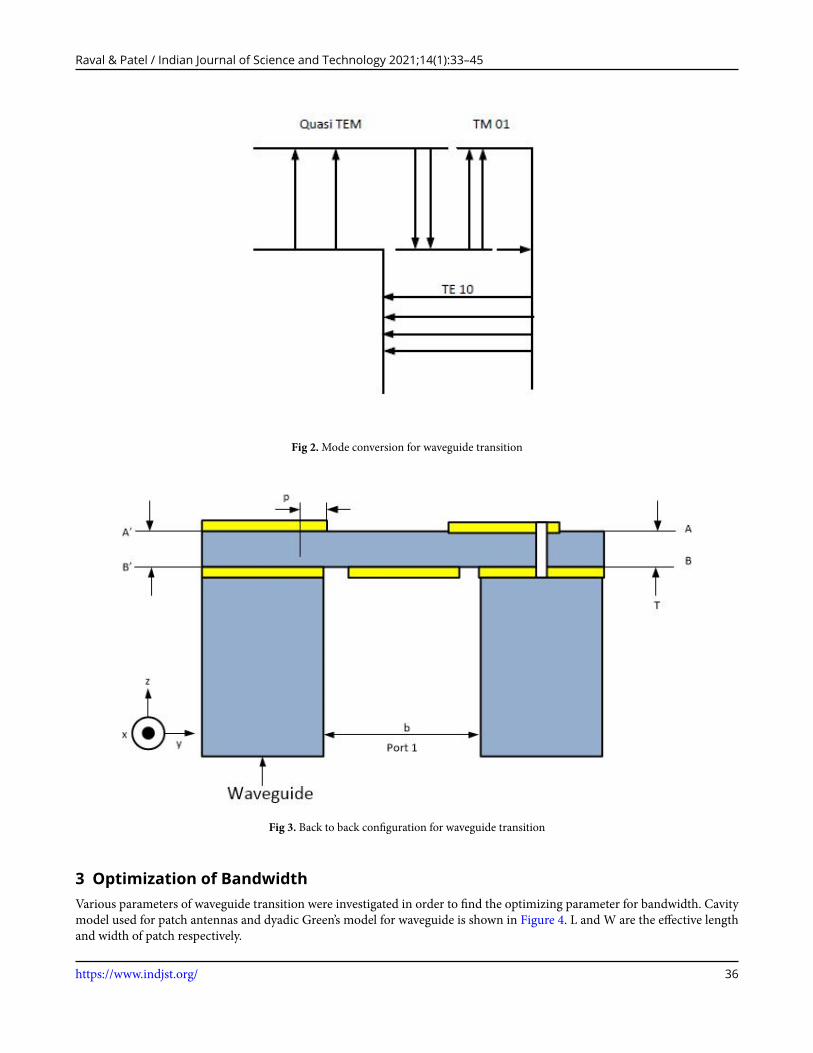
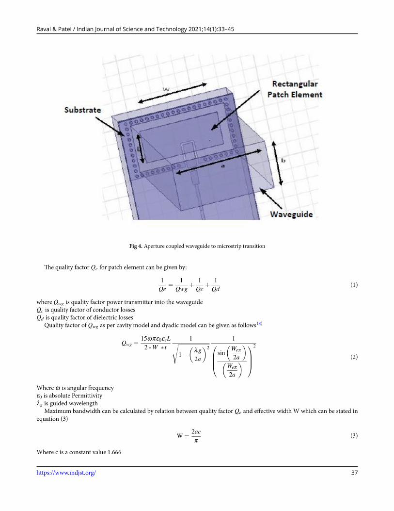
3 Optimization of BandwidthVarious parameters of waveguide transition were investigated in order to find the optimizing parameter for bandwidth. Cavitymodel used for patch antennas and dyadic Green’s model for waveguide is shown in Figure 4. L and W are the effective lengthand width of patch respectively.
https://www.indjst.org/ 36
Raval & Patel / Indian Journal of Science and Technology 2021;14(1):33–45
Fig 4. Aperture coupled waveguide to microstrip transition
The quality factor Qe for patch element can be given by:
1Qe
=1
Qwg+
1Qc
+1
Qd(1)
where Qwg is quality factor power transmitter into the waveguideQc is quality factor of conductor lossesQd is quality factor of dielectric losses
Quality factor of Qwg as per cavity model and dyadic model can be given as follows (8)
Qwg =15ωπε0εeL
2∗W ∗ t1√
1−(
λg2a
)2
1 sin(
Weπ2a
)(
Weπ2a
)
2
(2)
Where ω is angular frequencyε0 is absolute Permittivityλg is guided wavelength
Maximum bandwidth can be calculated by relation between quality factor Qe and effective width W which can be stated inequation (3)
W =2acπ
(3)
Where c is a constant value 1.666
https://www.indjst.org/ 37
Raval & Patel / Indian Journal of Science and Technology 2021;14(1):33–45
For minimum quality factory Qe , Qwg can be calculated as follows
Qwg | w =2aC
π=
15ωπε0εeL∗b4t
1√1−
(λg2a
)2
C(sinc)2 (4)
The bandwidth increases with increasing value of a, while effective width W is kept constant if broad bandwidth is required.Based on above equations it can be concluded that broadband response can be achieved by increasing the relative permittivity
εe and substrate thickness. Design presented in this paper was optimized for narrow band performance.Thus, thinner substratewith low relative permittivity has been selected for the design.
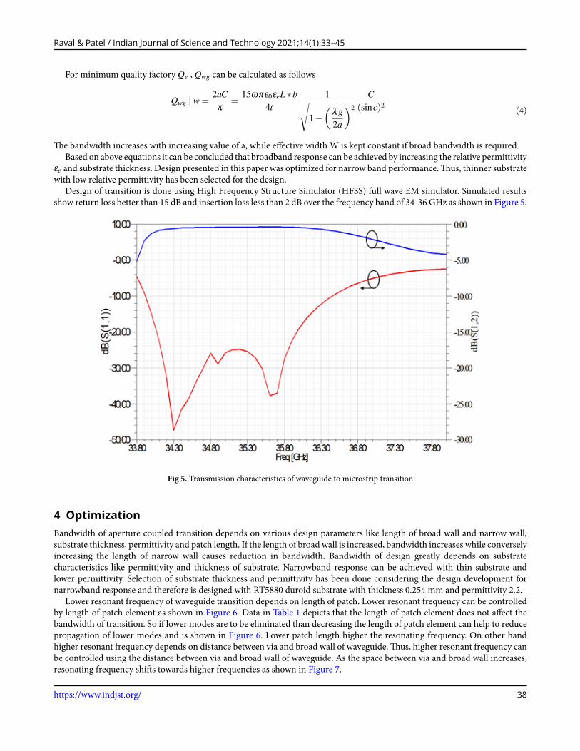
Design of transition is done using High Frequency Structure Simulator (HFSS) full wave EM simulator. Simulated resultsshow return loss better than 15 dB and insertion loss less than 2 dB over the frequency band of 34-36 GHz as shown in Figure 5.
Fig 5. Transmission characteristics of waveguide to microstrip transition
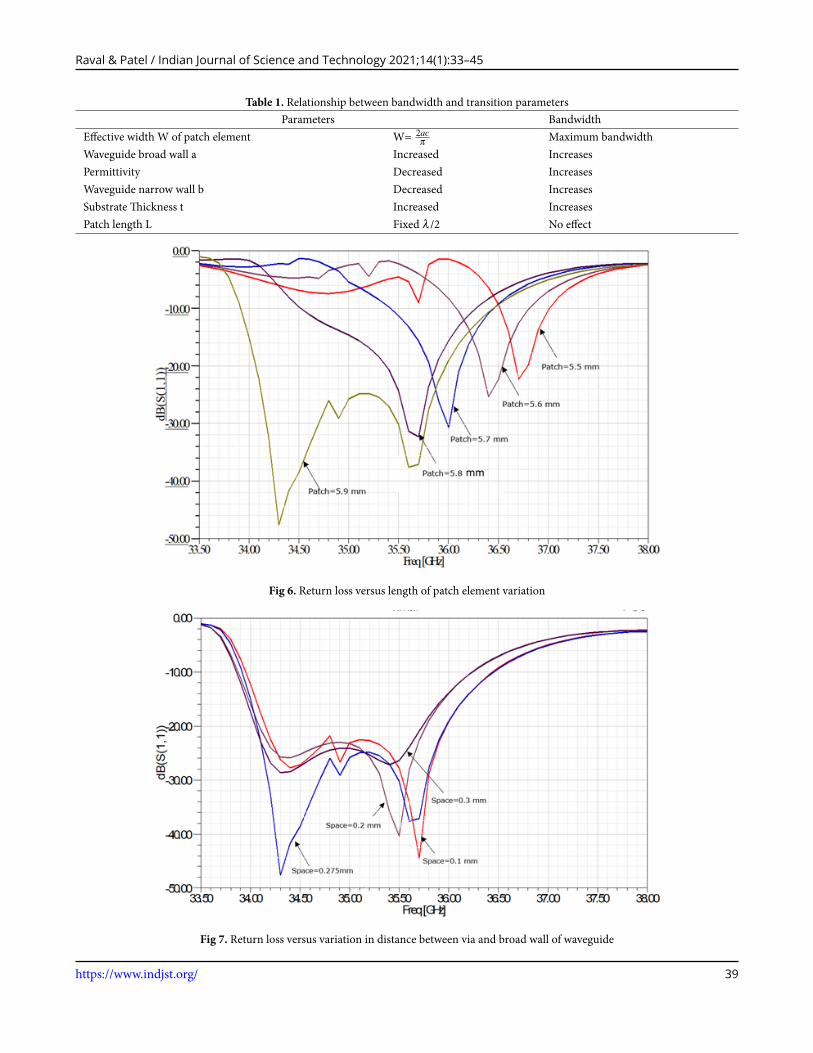
4 OptimizationBandwidth of aperture coupled transition depends on various design parameters like length of broad wall and narrow wall,substrate thickness, permittivity and patch length. If the length of broad wall is increased, bandwidth increases while converselyincreasing the length of narrow wall causes reduction in bandwidth. Bandwidth of design greatly depends on substratecharacteristics like permittivity and thickness of substrate. Narrowband response can be achieved with thin substrate andlower permittivity. Selection of substrate thickness and permittivity has been done considering the design development fornarrowband response and therefore is designed with RT5880 duroid substrate with thickness 0.254 mm and permittivity 2.2.
Lower resonant frequency of waveguide transition depends on length of patch. Lower resonant frequency can be controlledby length of patch element as shown in Figure 6. Data in Table 1 depicts that the length of patch element does not affect thebandwidth of transition. So if lower modes are to be eliminated than decreasing the length of patch element can help to reducepropagation of lower modes and is shown in Figure 6. Lower patch length higher the resonating frequency. On other handhigher resonant frequency depends on distance between via and broad wall of waveguide.Thus, higher resonant frequency canbe controlled using the distance between via and broad wall of waveguide. As the space between via and broad wall increases,resonating frequency shifts towards higher frequencies as shown in Figure 7.
https://www.indjst.org/ 38
Raval & Patel / Indian Journal of Science and Technology 2021;14(1):33–45
Table 1. Relationship between bandwidth and transition parametersParameters Bandwidth
Effective width W of patch element W= 2acπ Maximum bandwidth
Waveguide broad wall a Increased IncreasesPermittivity Decreased IncreasesWaveguide narrow wall b Decreased IncreasesSubstrate Thickness t Increased IncreasesPatch length L Fixed λ /2 No effect
Fig 6. Return loss versus length of patch element variation
Fig 7. Return loss versus variation in distance between via and broad wall of waveguide
https://www.indjst.org/ 39
Raval & Patel / Indian Journal of Science and Technology 2021;14(1):33–45
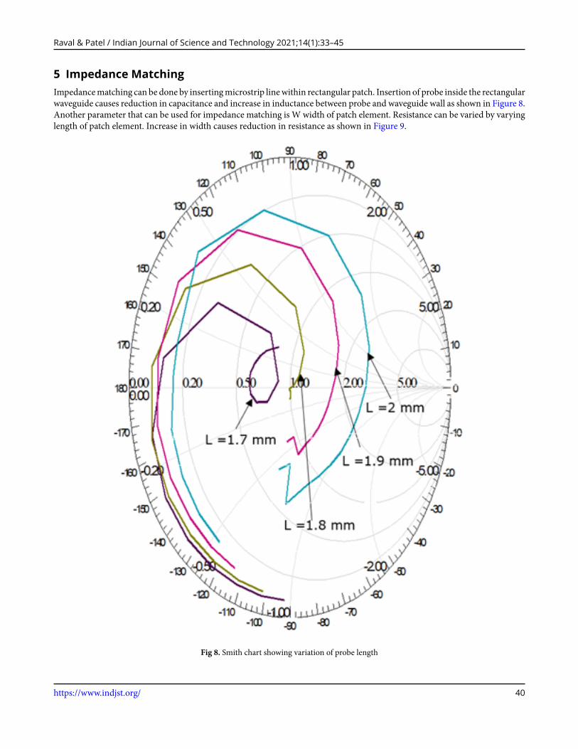
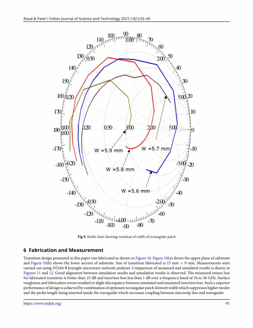
5 Impedance MatchingImpedancematching can be done by insertingmicrostrip linewithin rectangular patch. Insertion of probe inside the rectangularwaveguide causes reduction in capacitance and increase in inductance between probe and waveguide wall as shown in Figure 8.Another parameter that can be used for impedance matching is W width of patch element. Resistance can be varied by varyinglength of patch element. Increase in width causes reduction in resistance as shown in Figure 9.
Fig 8. Smith chart showing variation of probe length
https://www.indjst.org/ 40
Raval & Patel / Indian Journal of Science and Technology 2021;14(1):33–45
Fig 9. Smith chart showing variation of width of rectangular patch
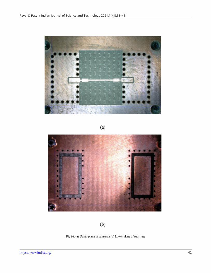
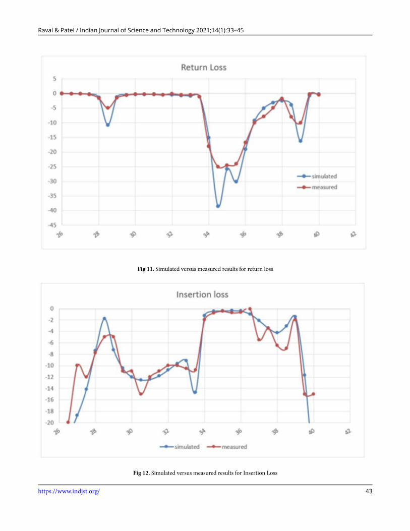
6 Fabrication and MeasurementTransition design presented in this paper was fabricated as shown in Figure 10. Figure 10(a) shows the upper plane of substrateand Figure 10(b) shows the lower section of substrate. Size of transition fabricated is 15 mm × 9 mm. Measurements werecarried out using N5244 B keysight microwave network analyzer. Comparison of measured and simulated results is shown inFigures 11 and 12. Good alignment between simulation results and simulation results is observed. The measured return lossfor fabricated transition is better than 25 dB and insertion loss less than 1 dB over a frequency band of 34 to 36 GHz. Surfaceroughness and fabrication errors resulted in slight discrepancy between simulated andmeasured insertion loss. Such a superiorperformance of design is achieved by combination of optimum rectangular patch elementwidthwhich suppresses highermodesand the probe length being inserted inside the waveguide which increases coupling between microstip line and waveguide.
https://www.indjst.org/ 41
Raval & Patel / Indian Journal of Science and Technology 2021;14(1):33–45
Fig 10. (a) Upper plane of substrate (b) Lower plane of substrate
https://www.indjst.org/ 42
Raval & Patel / Indian Journal of Science and Technology 2021;14(1):33–45
Fig 11. Simulated versus measured results for return loss
Fig 12. Simulated versus measured results for Insertion Loss
https://www.indjst.org/ 43
Raval & Patel / Indian Journal of Science and Technology 2021;14(1):33–45
7 ComparisonStructural characteristics and performance of various reported articles has been summarized in Table 2. Design presentedin (19) shows broadband performance compared to design in presented in this article as wedge shaped cavity increases thecoupling between microstrip line and waveguide. Design presented in (20) shows superior performance in terms of bandwidthcompared to present design as higher coupling is achieved as VM strip and aperture together act as ideal transformer andimproved coupling efficiency. Present work shows better performance compared to design presented in (21) in terms of returnloss performance. Transition design presented in (22) shows comparatively high insertion loss than present design as couplingbetween waveguide andmicrostrip line could bemaximized if two slots are placed very near to each other but due to fabricationconstraint minimum insertion loss achieved was -4.5 dB. Design presented in [25] shows superior performance than presentdesign in terms of loss as metallized groove technique is used around sidewalls of the rectangular waveguide. Present designshows much lower loss and improved coupling as compared to design presented in [26] over the same bandwidth. Based oncomparison with previously reported design, present work considerably shows improved performance in terms of bandwidth,return loss and insertion loss.
Table 2. Comparison of present work with previous worksReference Frequency (GHz) Substrate Thickness (mm) Substrate ε Insertion Loss (dB) Return Loss (dB) FBW (%)(23) 28-38 0.254 2.2 0.8 13 30.3(24) 7-13 0.35 10.2 0.82 Better than 16 dB 37(19) 47.6-76.7 0.508 2.94 Less than 1.3 dB Better than 12 dB 44.8(20) 57-82.7 0.254 2.2 Less than 5 dB Less than 10 dB 37.7(21) 26.65-30.20 0.254 2.33 0.3 dB Better than 20 dB 12(22) 50-70 0.254 5.8 1.9 Better than 10 dB 8.3Presentwork
33.5-38 0.254 2.2 Less than 1 dB Better than 25 dB 14.4
8 ConclusionDesign of waveguide transition presented in this study can be used for narrow and wideband applications by varying the designparameters. Optimum width of rectangular patch element for narrowband response has been proposed. Suppression of highermodes generated has also been proposed by optimizing the distance between via and broad wall of waveguide. Optimumcombination of patch width and spacing between via and broad wall leads to such improved performance. Simulation andmeasured results show that such low loss transition can be used practically and can be easily fabricated. Measured results forfabricated design show return loss better than 25 dB and insertion loss less than 1 dB over a frequency band of 34-36 GHz forback-to-back waveguide transition.
References1) Appleby R, Coward PR, Sinclair GN. Terahertz detection of illegal objects. In: Terahertz frequency detection and identification of materials and objects.
Springer. 2007;p. 225–240. Available from: https://doi.org/10.1007/978-1-4020-6503-3.2) Coward PR, Appleby R. Development of an illumination chamber for indoor millimeter-wave imaging. In: and others, editor. Passive Millimeter-wave
Imaging Technology VI and Radar Sensor Technology VII. 2003;p. 54–61. Available from: http://doi.org/10.1117/12.487031.3) Graauw TD, Helmich FP, Phillips TG, Stutzki J, Caux E, Whyborn ND, et al. The Herschel-heterodyne instrument for the far-infrared (HIFI). Astronomy
& Astrophysics. 2010;518. Available from: http://doi.org/10.1051/0004-6361/201014698.4) GrabherrW,MenzelW. ANew Transition fromMicrostrip Line to RectangularWaveguide. In: and others, editor. 22nd EuropeanMicrowave Conference.
1992. Available from: https://doi.org/10.1109/euma.1992.335862.5) GrabherrW, HuderWGB, Menzel W. Microstrip to waveguide transition compatible with MM-wave integrated circuits. IEEE Transactions on Microwave
Theory and Techniques. 1994;42(9):1842–1843. Available from: https://dx.doi.org/10.1109/22.310597.6) Shireen R, Shi S, Yao P, Schuetz CA,Macario J, Prather DW. CPW to rectangular waveguide transition on an ${{LiNbO}}_{3}$ substrate. IEEE Transactions
on Microwave Theory and Techniques. 2009;57(6):1494–1499. Available from: https://dx.doi.org/10.1109/tmtt.2009.2020673.7) Hyvonen L, Hujanen A. A compact MMIC-compatible microstrip to waveguide transition. IEEE MTT-S International Microwave Symposium Digest.
1996. Available from: https://doi.org/10.1109/mwsym.1996.511077.8) SimonW,WerthenM,Wolff I. A novel coplanar transmission line to rectangular waveguide transition. IEEEMTT-S International Microwave Symposium
Digest. 1998. Available from: https://doi.org/10.1109/mwsym.1998.689369.9) IizukaH,Watanabe T, Sato K, Nishikawa K. Millimeter-wavemicrostrip line to waveguide transition fabricated on a single layer dielectric substrate. IEICE
transactions on communications. 2002;85(6):1169–1177.
https://www.indjst.org/ 44

Raval & Patel / Indian Journal of Science and Technology 2021;14(1):33–45
10) IizukaH, SakakibaraK, KikumaN. Millimeter-Wave transition fromwaveguide to twomicrostrip lines using rectangular patch element. IEEETransactionson Microwave Theory and Techniques. 2007;55(5):899–905. Available from: https://dx.doi.org/10.1109/tmtt.2007.895139.
11) Cavanna T, Franzese E, Limiti E, Pelosi G, Selleri S, Suriani A. FEM-based evaluation of manufacturing tolerances on a millimeter-waves rectangularto coplanar waveguide transition. In: and others, editor. 15th International Conference on Microwaves, Radar and Wireless Communications. IEEE. .Available from: https://doi.org/10.1109/mikon.2004.1356894.
12) Poprawa F, Ziroff A, Ellinger F. A Novel Approach for a Periodic Structure Shielded Microstrip Line to RectangularWaveguide Transition. In: and others,editor. IEEE/MTT-S International Microwave Symposium. 2007. Available from: https://doi.org/10.1109/mwsym.2007.380572.
13) Zhang T, Li L, Zhu Z, Cui TJ. A Broadband Planar Balun Using Aperture-Coupled Microstrip-to-SIW Transition. IEEE Microwave and WirelessComponents Letters. 2019;p. 1–3. Available from: https://doi.org/10.1109/lmwc.2019.2922499.
14) Yakovlev AB, Ortiz S, Ozkar M, Mortazawi A, Steer MB. A waveguide-based aperture-coupled patch amplifier array-full-wave system analysis andexperimental validation. IEEE Transactions on MicrowaveTheory and Techniques. 2000;48(12):2692–2699. Available from: https://dx.doi.org/10.1109/22.899032.
15) Pérez-Escudero JM, Torres-García AE, Gonzalo R, Ederra I. A gap waveguide-based compact rectangular waveguide to a packaged microstrip inlinetransition. Applied Sciences. 2020;10(14). Available from: https://dx.doi.org/10.3390/app10144979.
16) Vidhi R, Patel A. Novel Design of waveguide to Microstrip Transition at Millimeter -Wave Frequencies. International Journal of Advanced Science andTechnology. 2020;29(04):6645–6665.
17) Zhang T, Li L, Zhu Z, Cui TJ. A Broadband Planar Balun Using Aperture-Coupled Microstrip-to-SIW Transition. IEEE Microwave and WirelessComponents Letters. 2019;p. 1–3. Available from: https://doi.org/10.1109/lmwc.2019.2922499.
18) Xu W, Liu F, Xu H. A novel ultra-wideband waveguide-to-microstrip transition for millimeter-wave applications. AIP Advances. 2016;6(10). Availablefrom: https://doi.org/10.1063/1.4964492.
19) Mohamed I, Sebak AR. Broadband transition of substrate-integrated waveguide-to-air-filled rectangular waveguide. IEEE Microwave and WirelessComponents Letters. 2018;28(11):966–968. Available from: https://dx.doi.org/10.1109/lmwc.2018.2871330.
20) AliakbarianH, EnayatiA,VandenboschGAE,RaedtWD. Novel low-cost end-wallmicrostrip-to-waveguide splitter transition. Progress In ElectromagneticsResearch. 2010;101:75–96. Available from: https://dx.doi.org/10.2528/pier09081805.
21) Deslandes D,WuK. Integratedmicrostrip and rectangular waveguide in planar form. IEEEMicrowave andWireless Components Letters. 2001;11(2):68–70.Available from: https://dx.doi.org/10.1109/7260.914305.
22) Lee HY, Jun DS, Moon SE, Kim EK, Park JH, Park KH. Wideband aperture coupled stacked patch type microstrip to waveguide transition for V-band.Asia-Pacific Microwave Conference. 2006. Available from: https://doi.org/10.1109/apmc.2006.4429440.
23) Li CL, Jin C,MaHQ, Shi XW. An inline waveguide-to-microstrip transition for widebandmillimeter-wave applications.Microwave andOptical TechnologyLetters. 2019. Available from: https://doi.org/10.1002/mop.32199.
24) Kim YJ, Kwak JH, Song H, Jiang X, Kim JP. Broadband aperture-coupled microstrip line to waveguide transition with loading a vertically mounted strip.Microwave and Optical Technology Letters. 2017;59(4):811–815. Available from: https://doi.org/10.1002/mop.30403.
https://www.indjst.org/ 45