Embed Size (px)
Citation preview
Dfi
MJa
b
c
d
a
ARRAA
KMsNOSS
1
iablastmb[tot
CT
0h
Applied Surface Science 301 (2014) 63–69
Contents lists available at ScienceDirect
Applied Surface Science
jou rn al h om ep age: www.elsev ier .com/ locate /apsusc
etermination of optical and mechanical properties of Nb2O5 thinlms for solar cells application
. Mazura, M. Szymanskab,c,∗, D. Kaczmareka, M. Kaliszb,c, D. Wojcieszaka,. Domaradzkia, F. Placidod
Faculty of Microsystem Electronics and Photonics, Wroclaw University of Technology, Janiszewskiego 11/17, Wrocław, PolandCentre for Material Testing and Mechatronics, Motor Transport Institute, Jagiellonska 80, Warsaw, PolandInstitute of Microelectronics and Optoelectronics, Warsaw University of Technology, Koszykowa 75, Warsaw, PolandUniversity of the West of Scotland, High Street, Paisley, PA1 2BE, and SUPA, Scottish Universities Physics Alliance, United Kingdom
r t i c l e i n f o
rticle history:eceived 9 October 2013eceived in revised form 23 January 2014ccepted 23 January 2014vailable online 2 February 2014
eywords:icrowave assisted reactive magnetron
puttering
a b s t r a c t
In this paper investigation results of niobium pentoxide thin films deposited by microwave assisted reac-tive magnetron sputtering process were described. Surface of prepared coatings was examined with theaid of atomic force microscope (AFM) operating in the contact-mode and in ultra high vacuum conditions.The surface of thin films was homogenous, crack free and exhibit low root mean square (RMS) rough-ness of about 0.34 nm. X-ray photoelectron spectroscopy (XPS) studies were performed to determine thechemical states of the niobium at the surface of thin films. Contact angle and surface free energy wereadditionally investigated to examine the surface properties of the deposited coatings. Optical propertiesof the Nb2O5 thin films showed, that prepared coatings were well transparent from 350 nm to longer
iobium pentoxideptical propertiesolar cellsurface and mechanical properties
wavelength range. Based on transmission and reflection measurements the values of refractive indexand extinction coefficient were determined. The antireflective coating based on Nb2O5 thin films for solarcells application was proposed. The hardness and Young’s modulus measurements were performed bythe nanoindentation technique. These investigations revealed that the hardness of the deposited coatingswas ca., 7 GPa. Also scratch tests were applied, which have shown that the Nb2O5 thin films were scratchresistant.
. Introduction
Thin oxide films based on various types of metals are increas-ngly applied for a wide range of optical and microelectronicpplications [1]. Among other, in case of optical applications, nio-ium oxide based materials are often used as high index and low
oss materials for e.g., optical waveguides [2], interference filters,ntireflective coatings or electroluminescent devices [3]. The mosttable form of niobium oxides is niobia (Nb2O5) and it is very attrac-ive for electronic applications. Nb2O5, along with other oxides of
etals from the Vth group, have also been investigated as possi-le candidates for thin film catalysts and corrosion barrier coatings4,5]. Recently, there has also been a considerable interest in using
he niobia as high permittivity dielectric to replace the existing gatexides in microelectronic devices [6–8]. Due to the exceptionalhermal stability and mechanical resistance of Nb2O5 compared∗ Corresponding author at: Corresponding author at: Motor Transport Institute,entre for Material Testing and Mechatronics, Jagiellonska 80, Warsaw, Poland.el.: +48 224385533.
E-mail address: [email protected] (M. Szymanska).
169-4332/$ – see front matter © 2014 Elsevier B.V. All rights reserved.ttp://dx.doi.org/10.1016/j.apsusc.2014.01.144
© 2014 Elsevier B.V. All rights reserved.
to traditional high permittivity materials, such thin films are veryattractive candidates for the above mentioned applications [9]. Thismaterial has also been appointed as a substitute of tantalum pen-toxide (ε′ = 27) for application in solid state capacitors [10]. Nb2O5is one of the useful optical materials for its desirable properties,such as stability in air and water, resistance to acid and base, highrefractive index (n = 2.4 at 550 nm), low extinction coefficient andhigh transparency in the UV–vis–NIR region [11]. It has been widelyused in e.g., intelligent windows [12], solar cells [13] and chemicalsensors [14]. Niobium oxide is also a promising material for counterelectrode in electrochromic devices, which can be used in case ofsolar cells, solar energy applications, sensors and display devices[15,16].
Structure of niobium oxide can exist in different polymorphicforms. There are at least three stable niobium oxides: NbO, NbO2and Nb2O5 and each has various electrical properties ranging fromconducting NbO to semiconducting NbO2 and insulating Nb2O5[17,18]. The properties of the niobium oxide thin films depend on
the type of deposition process and its parameters, such as reactivegas flow or pressure. It was shown by Ramirez et al. [18] that hard-ness of thin niobium oxide films increased from 3.9 GPa to 5.3 GPaby increasing the pressure and oxide content. On the other hand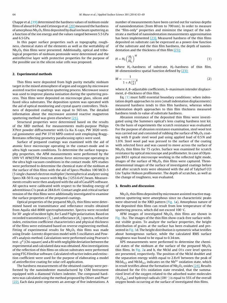
6 rface
Cfioaa
nNlat
2
tawcftnis
oXcB
aupUtwt(SmAatt
mffrioFueteouto
fen[
4 M. Mazur et al. / Applied Su
happe et al. [19] determined the hardness values of niobium oxidelms of about 6 GPa and Cetinorgu et al. [20] measured the hardnessf amorphous Nb2O5 films deposited by dual ion beam sputtering as
function of the ion energy and the values ranged between 5.5 GPand 6.5 GPa.
In this paper surface properties such as topography, rough-ess, chemical states of the elements as well as the wettability ofb2O5 thin films were presented. Additionally, optical and tribo-
ogical properties of niobium pentoxide were determined and thentireflective layer with protective properties for the purpose ofhe possible use in the silicon solar cells was proposed.
. Experimental methods
Thin films were deposited from high purity metallic niobiumarget in the mixed atmosphere of argon and oxygen by microwavessisted reactive magnetron sputtering process. Microwave sourceas used to improve plasma ionisation during the sputtering pro-
ess. Thin films were deposited on microscope glass, silicon andused silica substrates. The deposition system was operated withhe aid of optical monitoring and crystal quartz controllers. Thick-ess of deposited coatings was equal to 565 nm. The detailed
nformation about the microwave assisted reactive magnetronputtering method was given elsewhere [21].
Structural properties were determined based on the resultsf the XRD method. For measurements multi-purpose Philips’Pert powder diffractometer with Cu K� X-rays, PW 3020 verti-al goniometer and PW 3710 MPD control unit employing Bragg–rentano reflecting geometry parafocusing optics were used.
Surface of prepared coatings was examined with the aid oftomic force microscope operating in the contact-mode and inltra high vacuum conditions. To determine the surface topogra-hy properties, the AFM measurements were performed by theHV VT AFM/STM Omicron atomic force microscope operating in
he ultra high vacuum conditions in the contact mode. XPS studiesere performed to determine the chemical state of the niobium at
he surface of thin films with the aid of Specs Phoibos 100 MCD-55 single channel electron multiplier) hemispherical analyzer usingpecs XR-50 X-ray source with Mg K� (1253.6 eV) beam. Measure-ents results were then analyzed with the aid of CasaXPS software.ll spectra were calibrated with respect to the binding energy ofdventitious C1s peak at 284.8 eV. Contact angle and critical surfaceension of the thin films were additionally investigated to examinehe surface properties of the prepared coatings.
Optical properties of the prepared Nb2O5 thin films were deter-ined based on transmittance and reflectance results obtained
rom Aquila nkd-8000 spectrophotometer. Spectra were recordedor 30◦ angle of incident light, for S and P light polarization. Based onecorded transmittance (T�) and reflectance (R�) spectra, refractivendex, extinction coefficient characteristics and physical thicknessf the films were estimated based on reverse engineering method.itting of experimental results for Nb2O5 thin films was madesing Drude–Lorentz dispersion model with 5 oscillators and Pow-ll’s analysis method. Calculations were performed using Pearson’sest–�2 (Chi-square) and a fit with negligible deviation between thexperimental and calculated data was obtained. Also investigationsf the reflection of thin films on silicon substrates were performedsing FTG FilmStar software. Calculated refractive index and extinc-ion coefficient were used for the purpose of elaborating a modelf antireflective coating for solar cell application.
The hardness measurements of the obtained coatings were per-
ormed by the nanoindenter manufactured by CSM Instrumentquipped with a diamond Vickers indenter. The compound hard-ess was calculated using the method proposed by Oliver and Pharr22]. Each data point represents an average of five indentations. AScience 301 (2014) 63–69
number of measurements have been carried out for various depthsof nanoindentation (from 80 nm to 700 nm). In order to measurethe “film-only” properties and minimize the impact of the sub-strate a method of nanoindentation measurements approximationhas been implemented [23]. Measured hardness of the thin filmsdeposited on substrate can be expressed as a power-low functionof the substrate and the thin film hardness, the depth of nanoin-dentation and the thickness of thin film [23]:
H = HS
(Hf
HS
)M
(1)
where Hs–hardness of substrate, Hf–hardness of thin film,M–dimensionless spatial function defined by [23]:
M = 1
1 + A(
hd
)B(2)
where A, B–adjustable coefficients, h–maximum intender displace-ment, d–thickness of thin film.
Eq. (1) must fulfil essential boundary conditions: when inden-tation depth approaches to zero (small indentation displacements)measured hardness tends to thin film hardness, whereas whenindentation depth approaches to thin film thickness measuredhardness tends to value of substrate hardness.
Abrasion resistance of the deposited thin films were investi-gated using the Summers optical’s lens coating hardness test kit.On the basis of experiments the scratch resistance was evaluated.For the purpose of abrasion resistance examination, steel wool testwas carried out and consisted of rubbing the surface of Nb2O5 coat-ing with 0 grade steel wool pad using applied load of 0.5 N and1.0 N. Steel wool pad was pressed to the surface of the coatingwith selected force and was caused to move across the surface ofNb2O5 thin films for 75 cycles. Surface was examined for scratchresistance by optical microscope and profilometer. In case of Olym-pus BX51 optical microscope working in the reflected light mode,images of the surface of Nb2O5 thin films were captured. Three-dimensional images of the surface of investigated coatings beforeand after scratch tests were obtained with the aid of TalySurf CCILite Taylor Hobson profilometer. The depth of scratches, as well asthe change of roughness, was evaluated.
3. Results and discussion
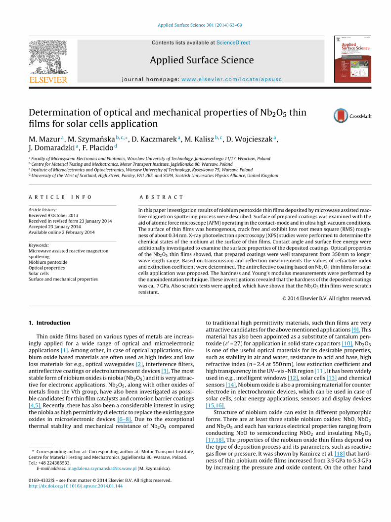
Nb2O5 thin films deposited by microwave assisted reactive mag-netron sputtering were amorphous since no characteristic peakswere observed in the XRD pattern (Fig. 1a). Amorphous nature ofthe deposited thin films can result from low temperature of thesputtering process, which did not exceed 100 ◦C.
AFM images of investigated Nb2O5 thin films are shown inFig. 1b,c. The images of the thin film show crack-free surface with-out visible grains. To analyze the surface properties, the heightdistribution of grains at the surface has been evaluated and pre-sented in Fig. 1d. The height distribution is symmetric what testifiesabout homogenous surface, while the calculated RMS surfaceroughness was found to be equal to 0.34 nm.
XPS measurements were performed to determine the chemi-cal states of the niobium at the surface of the prepared Nb2O5thin films. In Fig. 2a and b, the Nb3d and O1s core level spectraare presented, respectively. The position of the Nb3d doublet andthe separation energy width equal to 2.8 eV between the peak ofNb3d5/2 and Nb3d3/2 indicates on the Nb5+ oxidation state, whichin result testifies about the formation of Nb2O5 oxides [24]. Results
obtained for the O1s oxidation state revealed, that the summa-rized level of the oxygen related to the adsorbed water molecules(H2Oads) and hydroxyl radicals (OH−) is equal to 55% of the overalloxygen bonds occurring at the surface of investigated thin films.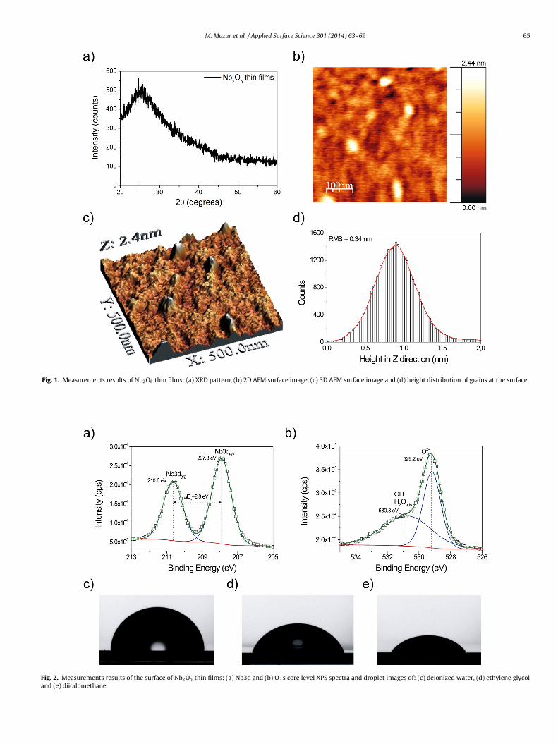
M. Mazur et al. / Applied Surface Science 301 (2014) 63–69 65
Fig. 1. Measurements results of Nb2O5 thin films: (a) XRD pattern, (b) 2D AFM surface image, (c) 3D AFM surface image and (d) height distribution of grains at the surface.
Fig. 2. Measurements results of the surface of Nb2O5 thin films: (a) Nb3d and (b) O1s core level XPS spectra and droplet images of: (c) deionized water, (d) ethylene glycoland (e) diiodomethane.
66 M. Mazur et al. / Applied Surface Science 301 (2014) 63–69
Fig. 3. Investigation results of optical properties of Nb O coatings: (a) transmission and reflection spectra taken for S and P polarization and 30◦ of light incidence, (b)r e coatt
fieReBwr
i5rmad[oft
rpsp
bPNf�pw
2 5
efractive and extinction coefficient spectra, (c) reflection coefficient of Si substrathe function of the light incidence angle.
The elemental composition of the surface of the deposited thinlms was evaluated based on relative sensitivity factors (R.S.F.) forach of the elements core levels and the area of proper spectra. The.S.F. were obtained from the CasaXPS software library and werequal to 2.85 and 8.46 for the O1s and Nb3d core levels, respectively.ased on these values the elemental composition of the surfaceas determined as 65.4 at.% and 34.6 at.% for oxygen and niobium,
espectively.Wettability measurement results revealed hydrophobic behav-
or of thin film surface. Contact angle was equal to 92.8◦, 69.0◦,5.3◦ for deionized water, ethylene glycol and diiodomethane,espectively. Droplet images of different liquids taken during theeasurements are shown in Fig. 2c–e. On the basis of the contact
ngle investigation, critical surface tension of the Nb2O5 thin filmseposited on SiO2 substrates was calculated using Zisman approach25]. Critical surface tension is often presented as the highest valuef surface tension of a liquid which will completely wet solid sur-ace. Results have shown that critical surface tension of the Nb2O5hin films was equal to 24.8 ± 1.7 mN/m.
Contact angle measurements in case of deionized waterevealed hydrophobic properties of the Nb2O5 thin film surface. Theotential uses of hydrophobicity of the prepared coatings includeelf-cleaning properties and it might favor influence on long-termerformance of the silicon solar cells with applied Nb2O5 coating.
The optical properties of investigated thin films were measuredy Aquila nkd8000 spectrophotometer, analyzed with the use ofro-Optix software and the results are shown in Fig. 3a,b. Depositedb2O5 coatings are transparent in the measured spectral range
rom 350 nm to 1000 nm and the average transmission level at = 600 nm is equal to about 80%. Spectra measured for S and Polarizations are slightly different due to the measurement, whichas performed at 30◦ of light incidence angle. Transmittance and
ed with Nb2O, and (d) reflection coefficient of coating deposited on Si substrate in
reflectance results were used to calculate the values of refractiveindex and extinction coefficient. In case of solar cell, it is necessaryto reduce its reflection coefficient in such a way, that the total lightradiation could be absorbed within the volume of the cell’s activematerial. For the crystalline silicon the reflection coefficient has thevalue of ca., 35–45% in the visible spectral range, therefore its reduc-tion is necessary. One of the ways to minimize this coefficient is toapply antireflective coating, which would be deposited on the frontsurface of the solar cell. However, the antireflective layer need tofulfil some basic conditions, i.e., it is required to achieve the lowestpossible value of the extinction coefficient, which would result in ahigh value of the transmission coefficient [26]. For example, oftenused coating as an antireflective layer for silicon solar cells is TiO2,which extinction coefficient is usually about 10−3 for the wave-length of 600 nm [21,27,28]. This allows on reflection losses reduc-tion from the solar cell to about 2–3%. In case of investigated Nb2O5thin films, the value of extinction coefficient for the � = 600 nm isequal to 3.59 × 10⁻⁵, while the refractive index is 2.30. Such valueof extinction coefficient shows, that deposited thin films almost donot absorb light in the visible light range. Moreover, due to hightransmission coefficient and suitable refractive index, the Nb2O5coatings could be used as antireflective layers for silicon solarcells.
To evaluate optical properties of designed Nb2O5 antireflectivelayer with specified thickness on silicon substrate, the FTG Film-Star software was used. The reflection coefficient of Si substratewas compared to the Si substrate coated with Nb2O5 thin film withthe thickness of 65 nm. It was calculated regarding to the value of
refractive index of the coating according to the following equation:narc × d = �opt
4(3)
M. Mazur et al. / Applied Surface Science 301 (2014) 63–69 67
F xide (i surem
wti
sttc4trasd1
hi6ramst2
m1woit
Hs
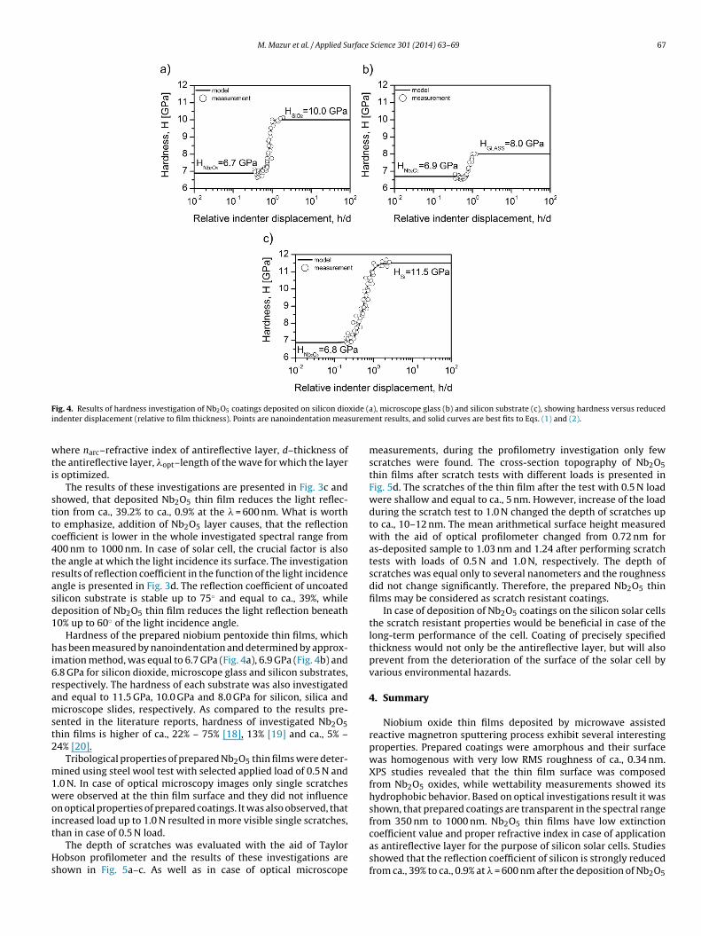
ig. 4. Results of hardness investigation of Nb2O5 coatings deposited on silicon diondenter displacement (relative to film thickness). Points are nanoindentation mea
here narc–refractive index of antireflective layer, d–thickness ofhe antireflective layer, �opt–length of the wave for which the layers optimized.
The results of these investigations are presented in Fig. 3c andhowed, that deposited Nb2O5 thin film reduces the light reflec-ion from ca., 39.2% to ca., 0.9% at the � = 600 nm. What is wortho emphasize, addition of Nb2O5 layer causes, that the reflectionoefficient is lower in the whole investigated spectral range from00 nm to 1000 nm. In case of solar cell, the crucial factor is alsohe angle at which the light incidence its surface. The investigationesults of reflection coefficient in the function of the light incidencengle is presented in Fig. 3d. The reflection coefficient of uncoatedilicon substrate is stable up to 75◦ and equal to ca., 39%, whileeposition of Nb2O5 thin film reduces the light reflection beneath0% up to 60◦ of the light incidence angle.
Hardness of the prepared niobium pentoxide thin films, whichas been measured by nanoindentation and determined by approx-
mation method, was equal to 6.7 GPa (Fig. 4a), 6.9 GPa (Fig. 4b) and.8 GPa for silicon dioxide, microscope glass and silicon substrates,espectively. The hardness of each substrate was also investigatednd equal to 11.5 GPa, 10.0 GPa and 8.0 GPa for silicon, silica andicroscope slides, respectively. As compared to the results pre-
ented in the literature reports, hardness of investigated Nb2O5hin films is higher of ca., 22% – 75% [18], 13% [19] and ca., 5% –4% [20].
Tribological properties of prepared Nb2O5 thin films were deter-ined using steel wool test with selected applied load of 0.5 N and
.0 N. In case of optical microscopy images only single scratchesere observed at the thin film surface and they did not influence
n optical properties of prepared coatings. It was also observed, thatncreased load up to 1.0 N resulted in more visible single scratches,
han in case of 0.5 N load.The depth of scratches was evaluated with the aid of Taylorobson profilometer and the results of these investigations are
hown in Fig. 5a–c. As well as in case of optical microscope
a), microscope glass (b) and silicon substrate (c), showing hardness versus reducedent results, and solid curves are best fits to Eqs. (1) and (2).
measurements, during the profilometry investigation only fewscratches were found. The cross-section topography of Nb2O5thin films after scratch tests with different loads is presented inFig. 5d. The scratches of the thin film after the test with 0.5 N loadwere shallow and equal to ca., 5 nm. However, increase of the loadduring the scratch test to 1.0 N changed the depth of scratches upto ca., 10–12 nm. The mean arithmetical surface height measuredwith the aid of optical profilometer changed from 0.72 nm foras-deposited sample to 1.03 nm and 1.24 after performing scratchtests with loads of 0.5 N and 1.0 N, respectively. The depth ofscratches was equal only to several nanometers and the roughnessdid not change significantly. Therefore, the prepared Nb2O5 thinfilms may be considered as scratch resistant coatings.
In case of deposition of Nb2O5 coatings on the silicon solar cellsthe scratch resistant properties would be beneficial in case of thelong-term performance of the cell. Coating of precisely specifiedthickness would not only be the antireflective layer, but will alsoprevent from the deterioration of the surface of the solar cell byvarious environmental hazards.
4. Summary
Niobium oxide thin films deposited by microwave assistedreactive magnetron sputtering process exhibit several interestingproperties. Prepared coatings were amorphous and their surfacewas homogenous with very low RMS roughness of ca., 0.34 nm.XPS studies revealed that the thin film surface was composedfrom Nb2O5 oxides, while wettability measurements showed itshydrophobic behavior. Based on optical investigations result it wasshown, that prepared coatings are transparent in the spectral rangefrom 350 nm to 1000 nm. Nb2O5 thin films have low extinction
coefficient value and proper refractive index in case of applicationas antireflective layer for the purpose of silicon solar cells. Studiesshowed that the reflection coefficient of silicon is strongly reducedfrom ca., 39% to ca., 0.9% at � = 600 nm after the deposition of Nb2O5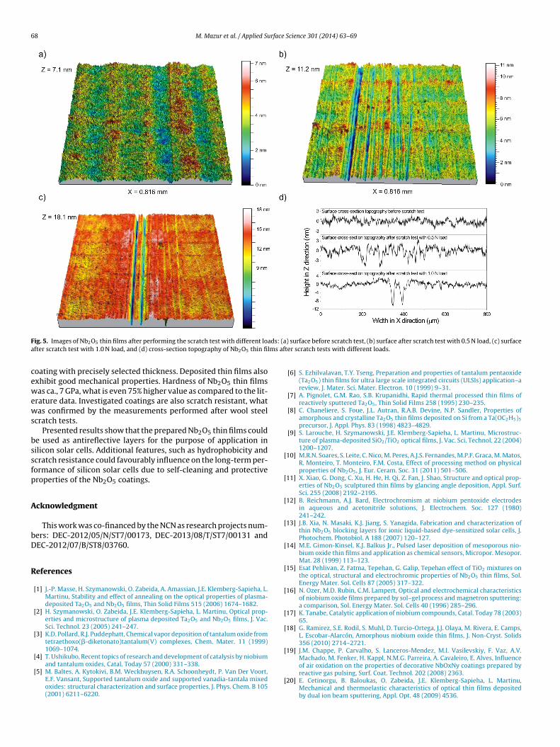
68 M. Mazur et al. / Applied Surface Science 301 (2014) 63–69
F ads: (aa lms af
cewews
bssfp
A
bD
R
[
[
[
[
[
[
[
[
[
[
ig. 5. Images of Nb2O5 thin films after performing the scratch test with different lofter scratch test with 1.0 N load, and (d) cross-section topography of Nb2O5 thin fi
oating with precisely selected thickness. Deposited thin films alsoxhibit good mechanical properties. Hardness of Nb2O5 thin filmsas ca., 7 GPa, what is even 75% higher value as compared to the lit-
rature data. Investigated coatings are also scratch resistant, whatas confirmed by the measurements performed after wool steel
cratch tests.Presented results show that the prepared Nb2O5 thin films could
e used as antireflective layers for the purpose of application inilicon solar cells. Additional features, such as hydrophobicity andcratch resistance could favourably influence on the long-term per-ormance of silicon solar cells due to self-cleaning and protectiveroperties of the Nb2O5 coatings.
cknowledgment
This work was co-financed by the NCN as research projects num-ers: DEC-2012/05/N/ST7/00173, DEC-2013/08/T/ST7/00131 andEC-2012/07/B/ST8/03760.
eferences
[1] J.-P. Masse, H. Szymanowski, O. Zabeida, A. Amassian, J.E. Klemberg-Sapieha, L.Martinu, Stability and effect of annealing on the optical properties of plasma-deposited Ta2O5 and Nb2O5 films, Thin Solid Films 515 (2006) 1674–1682.
[2] H. Szymanowski, O. Zabeida, J.E. Klemberg-Sapieha, L. Martinu, Optical prop-erties and microstructure of plasma deposited Ta2O5 and Nb2O5 films, J. Vac.Sci. Technol. 23 (2005) 241–247.
[3] K.D. Pollard, R.J. Puddephatt, Chemical vapor deposition of tantalum oxide fromtetraethoxo(�-diketonato)tantalum(V) complexes, Chem. Mater. 11 (1999)1069–1074.
[4] T. Ushikubo, Recent topics of research and development of catalysis by niobium
and tantalum oxides, Catal. Today 57 (2000) 331–338.[5] M. Baltes, A. Kytokivi, B.M. Weckhuysen, R.A. Schoonheydt, P. Van Der Voort,E.F. Vansant, Supported tantalum oxide and supported vanadia-tantala mixedoxides: structural characterization and surface properties, J. Phys. Chem. B 105(2001) 6211–6220.
[
) surface before scratch test, (b) surface after scratch test with 0.5 N load, (c) surfaceter scratch tests with different loads.
[6] S. Ezhilvalavan, T.Y. Tseng, Preparation and properties of tantalum pentaoxide(Ta2O5) thin films for ultra large scale integrated circuits (ULSIs) application–areview, J. Mater. Sci. Mater. Electron. 10 (1999) 9–31.
[7] A. Pignolet, G.M. Rao, S.B. Krupanidhi, Rapid thermal processed thin films ofreactively sputtered Ta2O5, Thin Solid Films 258 (1995) 230–235.
[8] C. Chaneliere, S. Foue, J.L. Autran, R.A.B. Devine, N.P. Sandler, Properties ofamorphous and crystalline Ta2O5 thin films deposited on Si from a Ta(OC2H5)5
precursor, J. Appl. Phys. 83 (1998) 4823–4829.[9] S. Larouche, H. Szymanowski, J.E. Klemberg-Sapieha, L. Martinu, Microstruc-
ture of plasma-deposited SiO2/TiO2 optical films, J. Vac. Sci. Technol. 22 (2004)1200–1207.
10] M.R.N. Soares, S. Leite, C. Nico, M. Peres, A.J.S. Fernandes, M.P.F. Graca, M. Matos,R. Monteiro, T. Monteiro, F.M. Costa, Effect of processing method on physicalproperties of Nb2O5, J. Eur. Ceram. Soc. 31 (2011) 501–506.
11] X. Xiao, G. Dong, C. Xu, H. He, H. Qi, Z. Fan, J. Shao, Structure and optical prop-erties of Nb2O5 sculptured thin films by glancing angle deposition, Appl. Surf.Sci. 255 (2008) 2192–2195.
12] B. Reichmann, A.J. Bard, Electrochromism at niobium pentoxide electrodesin aqueous and acetonitrile solutions, J. Electrochem. Soc. 127 (1980)241–242.
13] J.B. Xia, N. Masaki, K.J. Jiang, S. Yanagida, Fabrication and characterization ofthin Nb2O5 blocking layers for ionic liquid-based dye-sensitized solar cells, J.Photochem. Photobiol. A 188 (2007) 120–127.
14] M.E. Gimon-Kinsel, K.J. Balkus Jr., Pulsed laser deposition of mesoporous nio-bium oxide thin films and application as chemical sensors, Micropor. Mesopor.Mat. 28 (1999) 113–123.
15] Esat Pehlivan, Z. Fatma, Tepehan, G. Galip, Tepehan effect of TiO2 mixtures onthe optical, structural and electrochromic properties of Nb2O5 thin films, Sol.Energy Mater. Sol. Cells 87 (2005) 317–322.
16] N. Ozer, M.D. Rubin, C.M. Lampert, Optical and electrochemical characteristicsof niobium oxide films prepared by sol–gel process and magnetron sputtering:a comparison, Sol. Energy Mater. Sol. Cells 40 (1996) 285–296.
17] K. Tanabe, Catalytic application of niobium compounds, Catal. Today 78 (2003)65.
18] G. Ramirez, S.E. Rodil, S. Muhl, D. Turcio-Ortega, J.J. Olaya, M. Rivera, E. Camps,L. Escobar-Alarcón, Amorphous niobium oxide thin films, J. Non-Cryst. Solids356 (2010) 2714–2721.
19] J.M. Chappe, P. Carvalho, S. Lanceros-Mendez, M.I. Vasilevskiy, F. Vaz, A.V.Machado, M. Fenker, H. Kappl, N.M.G. Parreira, A. Cavaleiro, E. Alves, Influenceof air oxidation on the properties of decorative NbOxNy coatings prepared by
reactive gas pulsing, Surf. Coat. Technol. 202 (2008) 2363.20] E. Cetinorgu, B. Baloukas, O. Zabeida, J.E. Klemberg-Sapieha, L. Martinu,Mechanical and thermoelastic characteristics of optical thin films depositedby dual ion beam sputtering, Appl. Opt. 48 (2009) 4536.
rface
[
[
[
[
[
[
[
prospective material for transparent electronics, Thin Solid Films 520 (2012)
M. Mazur et al. / Applied Su
21] M. Mazur, D. Wojcieszak, J. Domaradzki, D. Kaczmarek, S. Song, F. Placido,TiO2/SiO2 multilayer as an antireflective and protective coating deposited bymicrowave assisted magnetron sputtering, Opto-Electron. Rev. 21 (2) (2013)233–238.
22] W.C. Oliver, G.M. Pharr, An improved technique for determining hardness andelastic modulus using load and displacement sensing indentation experiments,J. Mater. Res. 7 (1992) 1564–1583.
23] Y.-G. Jung, B.R. Lawn, M. Martyniuk, H. Huang, X.Z. Hu, Evaluation of elastic
modulus and hardness of thin films by nanoindentation, J. Mater. Res. 19 (2004)3076–3080.24] J. Moulder, W. Stickle, P. Sobol, K. Bomben, Handbook of X-ray PhotoelectronSpectroscopy, Physical Electronics Inc., United States of America, 1995, ISBN0-9648124-1-X.
[
Science 301 (2014) 63–69 69
25] D.Y. Kwok, A.W. Neumann, Contact angle measurement and contact angle inter-pretation, Adv. Colloid Interface 81 (1999) 167–249.
26] K. Drabczyk, P. Panek, Silicon-based solar cells–Characteristics and productionprocesses, Institute of Metallurgy and Materials Science of Polish Academy ofSciences, Cracov, Poland, 2012, pp. 18–21, ISBN 978-83-62098-08-8.
27] K. Sieradzka, M. Mazur, D. Wojcieszak, J. Domaradzki, D. Kaczmarek, E.Prociów, P-type transparent Ti–V oxides semiconductor thin film as a
3472–3476.28] Y. Shen, H. Yu, J. Yao, S. Shao, Z. Fan, H. He, J. Shao, Investigation on properties
of TiO2 thin films deposited at different oxygen pressures, Opt. Laser Technol.40 (2008) 550–554.


