Embed Size (px)
Citation preview
Appl Phys A (2010) 101: 633–638DOI 10.1007/s00339-010-5915-6
Cathodoluminescence degradation of PLD thin films
H.C. Swart · E. Coetsee · J.J. Terblans ·O.M. Ntwaeaborwa · P.D. Nsimama · F.B. Dejene ·J.J. Dolo
Received: 22 November 2009 / Accepted: 15 June 2010 / Published online: 16 July 2010© Springer-Verlag 2010
Abstract The cathodoluminescence (CL) intensities ofY2SiO5:Ce3+, Gd2O2S:Tb3+ and SrAl2O4:Eu2+,Dy3+phosphor thin films that were grown by pulsed laser deposi-tion (PLD) were investigated for possible application in lowvoltage field emission displays (FEDs) and other infrastruc-ture applications. Several process parameters (backgroundgas, laser fluence, base pressure, substrate temperature, etc.)were changed during the deposition of the thin films. Atomicforce microscopy (AFM) was used to determine the surfaceroughness and particle size of the different films. The lay-ers consist of agglomerated nanoparticle structures. Sam-ples with good light emission were selected for the electrondegradation studies. Auger electron spectroscopy (AES) andCL spectroscopy were used to monitor changes in the sur-face chemical composition and luminous efficiency of thethin films. AES and CL spectroscopy were done with 2 keVenergy electrons. Measurements were done at 1 × 10⁻⁶ Torroxygen pressure. The formation of different oxide layersduring electron bombardment was confirmed with X-rayphotoelectron spectroscopy (XPS). New non-luminescentlayers that formed during electron bombardment were re-sponsible for the degradation in light intensity. The adven-titious C was removed from the surface in all three casesas volatile gas species, which is consistent with the electronstimulated surface chemical reaction (ESSCR) model. ForY2SiO5:Ce3+ a luminescent SiO2 layer formed during theelectron bombardment. Gd2O3 and SrO thin films formedon the surfaces of Gd2O2S:Tb3+ and SrAl2O4:Eu2+,Dy3+,respectively, due to ESSCRs.
H.C. Swart (�) · E. Coetsee · J.J. Terblans · O.M. Ntwaeaborwa ·P.D. Nsimama · F.B. Dejene · J.J. DoloDepartment of Physics, University of the Free State,P.O. Box 339, Bloemfontein 9300, South Africae-mail: [email protected]: +27-51-401-3507
1 Introduction
Luminescent light emitting materials based on lanthanidephosphors are emerging rapidly and are revolutionizing thedisplay and lighting industries. It is anticipated that ox-ide phosphors have the potential for replacing old phos-phors in conventional displays. However, significantly im-proved performance of displays demands high-quality phos-phors having sufficient brightness and long-term stability.Many authors have used rare-earth-doped oxide particlesas phosphors in various display applications such as field-emission displays (FEDs) [1], plasma display panels (PDPs)[2] and cathode ray tubes (CRTs) [3]. Hillie et al. [4, 5] re-ported the degradation of sulfide-based thin films that weresuccessfully prepared with pulsed laser deposition (PLD).Gd2O3:Eu3+ thin films were proposed as one of the mostpromising oxide-based red phosphor systems [1]. It is there-fore worthwhile to also include other dopants such as Tbin our investigation to obtain other emission colours. Due tothe 5D0–7F2 transition within Eu3+, Gd2O3:Eu3+ shows redluminescence properties and emits red light at a wavelengthof 612 nm [6, 7]. X-ray microscopes hold the potential toprobe biological specimens in their natural state and, due tothe shorter wavelength, can provide much enhanced resolu-tions over optical microscopy. A phosphor screen is neededfor measuring these X-rays in conjunction with a photodi-ode [8]. One way of achieving this is to use a phosphorcoating which absorbs incoming X-rays and subsequentlyrelaxes, emitting visible, or near-visible, electromagneticradiation. The mentioned radiation may then be detectedby using a photodiode. Y2SiO5:Ce3+, Gd2O2S:Tb3+ andSrAl2O4:Eu2+,Dy3+ phosphor thin films are excellent can-didates for these applications.
Rare-earth-ion-doped strontium aluminate, SrAl2O4:Eu2+,Dy3+, is an important material for long-persistent

634 H.C. Swart et al.
luminescence. SrAl2O4 has a stuffed tridymite structure,which is constructed by corner-shared AlO4 tetrahedrons,and large divalent cations, Sr2+ ions, to occupy the inter-stitial sites to compensate the charge imbalance [9]. Sincethe ionic radii are similar, doped Eu2+ ions and Dy3+ ionsare suggested to substitute Sr2+ sites within the stuffedtridymite structure. The 4f–5d transition of Eu2+ ions inthe SrAl2O4 matrix provides a broadband emission centredat about 520 nm [10]. Dy3+ is a co-activator, which cantrap holes from the 4f–5d transition of Eu2+ ions, therebyleading to long-persistent luminescence [11].
Luminescence in Y2SiO5:Ce3+ occurs due to character-istic transitions in the Ce3+ ion itself. Y2SiO5 has a wideband gap of about 7.4 eV; doping it with an activator such asCe3+ creates an energy level structure inside the wide bandgap where the 5d to 4f transition takes place. Splitting ofthe 4f energy level into the 2F5/2 and 2F7/2 energy levels isdue to the 4f1 electron in Ce3+ having the ability to exhibita +1/2 and a −1/2 spin [12, 13]. This creates the expecta-tion of a luminescent spectrum with two main peaks in theblue region (between 400 and 500 nm). However, reports onbroadband and double-shoulder spectra have been found.
This paper reports the cathodoluminescence (CL) degra-dation of Y2SiO5:Ce3+, Gd2O2S:Tb3+ and SrAl2O4:Eu2+,Dy3+ phosphor thin films that were deposited by laser abla-tion. The purpose was to test the stability of these thin filmsunder electron bombardment in oxygen atmospheres. Thefilms were selected from a series of samples prepared withPLD under different experimental conditions.
2 Experimental setup
Several SrAl2O4:Eu2+,Dy3+, Gd2O2S:Tb and Y2SiO5:Ce3+phosphor thin films were deposited with PLD on Si(100)substrates. Three thin films were selected from these. Theselected film of SrAl2O4:Eu2+,Dy3+ was deposited in vac-uum at a pressure of 10−6 Torr, substrate temperatureof 200°C, frequency of 8 Hz and fluence of 1.2±0.2 J cm−2.The Gd2O2S:Tb3+ thin film was deposited at an O2 pressureof 0.3 Torr, substrate temperature of 600°C, frequency of10 Hz and fluence of 6.2±0.2 J cm−2 and the Y2SiO5:Ce3+thin film was deposited at an Ar pressure of 0.455 Torr,substrate temperature of 600°C, frequency of 8 Hz and flu-ence of 1.6 ± 0.2 J cm−2. The thin films obtained were de-graded under electron bombardment at an O2 pressure of1 × 10−6 Torr, 2 keV electron energy and 10 μA electronbeam current with an average beam diameter of 800 μm. TheCL and degradation measurements were made in an UHVchamber with a PHI model 549 system and the CL datawere collected with an Ocean Optics S2000 spectrometer.Auger electron spectroscopy (AES) and CL spectroscopywere used to simultaneously monitor changes in the surfacechemical composition and luminous efficiency of the thinfilms.
3 Results and discussion
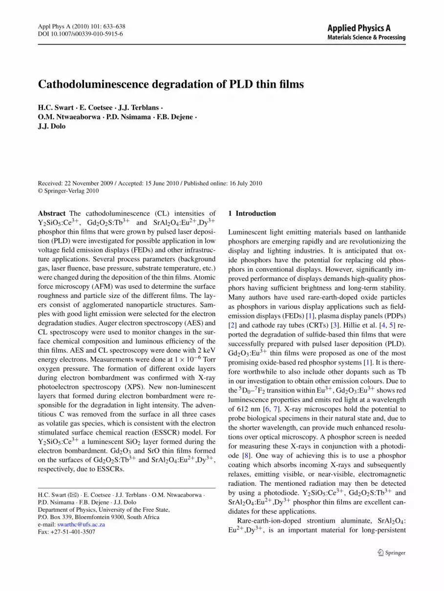
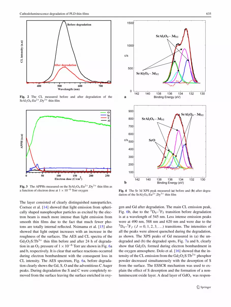
The atomic force microscopy (AFM) picture of the SrAl2O4:Eu2+,Dy3+ thin film is shown in Fig. 1. The structures (par-ticles) on the surface are not clearly distinguishable, whichis in agreement with previous results obtained for vacuumsamples [14]. Smooth phosphor layers are normally ob-tained with PLD in vacuum. Nanosized particles formedduring the deposition process in the O2 and Ar atmospheres.The sizes varied from 36 to 43 nm for the films depositedin O2 and Ar, respectively. Figure 2 shows the CL spec-tra of the vacuum thin film before and after degradation atan O2 pressure of 1 × 10⁻⁶ Torr. The film gave a greenemission with a peak at 520 nm. The peak is attributed to4f65d1 → 4f7 transitions of Eu2+. The intensity of the peakafter degradation decreased to about 30% of the original in-tensity before degradation. The CL results indicate that thephosphor layer has degraded during electron bombardment.Figure 3 shows the Auger peak-to-peak height (APPH) ver-sus electron dose results for the SrAl2O4:Eu2+,Dy3+ thinfilm degraded at the 1 × 10⁻⁶ Torr oxygen pressure. TheC desorbed from the surface while the O initially increasedduring electron bombardment. AES is only sensitive for thetop few surface layers. The Sr, Al and O atoms were initiallycovered by the C atoms. With the removal of the C the toplayers of the phosphor were exposed to the electron beamand this therefore resulted in an increase in the AES intensi-ties of the elements. The X-ray photoelectron spectroscopy(XPS) spectra measured (a) before and (b) after degradation,Fig. 4a and b, indicated that SrO formed during the degrada-tion process. Electron stimulated surface chemical reactions(ESSCRs) are partially responsible for the degradation inCL intensity.
The AFM picture of the PLD Gd2O2S:Tb3+ thin film de-posited at an O2 pressure of 0.3 Torr is shown in Fig. 5.
Fig. 1 The AFM picture of the PLD SrAl2O4:Eu2+,Dy3+ thin filmdeposited in vacuum
Cathodoluminescence degradation of PLD thin films 635
Fig. 2 The CL measured before and after degradation of theSrAl2O4:Eu2+,Dy3+ thin film
Fig. 3 The APPHs measured on the SrAl2O4:Eu2+,Dy3+ thin film asa function of electron dose at 1 × 10⁻⁶ Torr oxygen
The layer consisted of clearly distinguished nanoparticles.Coetsee et al. [14] showed that light emission from spheri-cally shaped nanophosphor particles as excited by the elec-tron beam is much more intense than light emission fromsmooth thin films due to the fact that much fewer pho-tons are totally internal reflected. Nsimama et al. [15] alsoshowed that light output increases with an increase in theroughness of the surfaces. The AES and CL spectra of theGd2O2S:Tb3+ thin film before and after 24 h of degrada-tion in an O2 pressure of 1 × 10⁻⁶ Torr are shown in Fig. 6aand b, respectively. It is clear that surface reactions occurredduring electron bombardment with the consequent loss inCL intensity. The AES spectrum, Fig. 6a, before degrada-tion clearly shows the Gd, S, O and the adventitious C Augerpeaks. During degradation the S and C were completely re-moved from the surface leaving the surface enriched in oxy-
Fig. 4 The Sr 3d XPS peak measured (a) before and (b) after degra-dation of the SrAl2O4:Eu2+,Dy3+ thin film
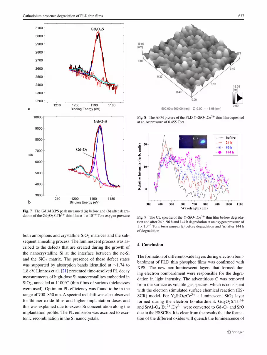
gen and Gd after degradation. The main CL emission peak,Fig. 6b, due to the 5D4–7F5 transition before degradationis at a wavelength of 545 nm. Less intense emission peakswere at 490 nm, 588 nm and 620 nm and were due to the5D4–7FJ (J = 0,1,2,3, . . .) transitions. The intensities ofall the peaks were almost quenched during the degradation,as shown. The XPS peaks of Gd measured in (a) the un-degraded and (b) the degraded spots, Fig. 7a and b, clearlyshow that Gd2O3 formed during electron bombardment inthe oxygen atmosphere. Dolo et al. [16] showed that the in-tensity of the CL emission from the Gd2O2S:Tb3+ phosphorpowder decreased simultaneously with the desorption of Sfrom the surface. The ESSCR mechanism was used to ex-plain the effect of S desorption and the formation of a non-luminescent oxide layer. A dead layer of GdOx was respon-

636 H.C. Swart et al.
Fig. 5 The AFM picture of the PLD Gd2O2S:Tb3+ thin film depositedat an O2 pressure of 0.3 Torr
sible for the degradation of the CL intensity with an increasein electron dose.
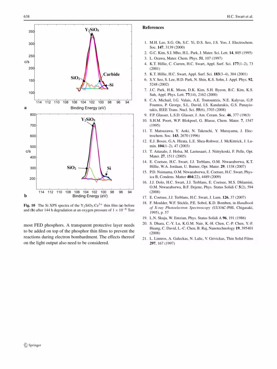
The AFM image of the Y2SiO5:Ce3+ thin film ablatedat an Ar pressure of 0.455 Torr is shown in Fig. 8. Thelayer consists of nanoparticles with a size in the order of30 nm and maximum height of about 20 nm. The particlesare spherical and evenly distributed on the surface. Exceptfor small changes in the Si low energy AES peak shapes,monitored for 144 h during electron bombardment of thethin film at 1 × 10⁻⁶ Torr, no severe changes were detectedin the APPHs (AES results not shown here). Figure 9 showsthe CL spectra taken before degradation and after 24, 96 and144 h of degradation. It is clear from Fig. 9 that there wasa definite decrease in the CL intensity measured at 440 nmwhile a second broadband peak emerged at 650 nm, whichincreased with an increase in the degradation time leadingto a broad spectrum ranging from 400 to 850 nm. From theinset images (i) before degradation and (ii) after 144 h ofdegradation it is clear that the blue colour changed (the sameas with the powders [17]) to a whitish colour with the brightarea the spot of maximum degradation due to the shape ofthe electron beam, which is more intensified in the centre ofthe beam. Coetsee et al. [17] also showed for Y2SiO5:Ce3+phosphor powders that after 24 h electron bombardment asecond broadband peak emerged at around 650 nm. Thiswas a result of a defect level in SiO2 (1.9 eV/650 nm) thatformed on the surface due to ESSCRs. Figure 10 shows theGaussian peak fits of the XPS data obtained from (a) the un-degraded and (b) the 144 h degraded spots. The existence ofsilica, although not as severe as in the case of the powder,is again proven by the small Si (103.4 eV) 2p peak of SiO2.The SiO2 was confirmed from the O 1s peak fits as well.The electron bombardment during the degradation processin the presence of O2 gas causes the Y–Si–O bonds to break
Fig. 6 (a) The AES spectra of the Gd2O2S:Tb3+ thin film beforeand after degradation at 1 × 10⁻⁶ Torr oxygen pressure. (b) The CLspectra of the Gd2O2S:Tb3+ thin film before and after degradation at1 × 10−6 Torr oxygen pressure
and form new chemical compounds. The peak situated at100 eV in (a) is due to SiC [18] formed on the surface asa result of a chemical reaction between Si and the adventi-tious C. Skuja and Entzian [19] reported two peak intensi-ties for SiO2 at 1.9 eV (650 nm) and 2.7 eV (459 nm) with atheory that the two peaks are related to intrinsic defects in-volving cleavage of the Si–O bonds. A definite contributionfrom the SiO2 1.9 eV defect to the transition from the higher5d levels to the 4f7/2 levels leads to the increase in the CLintensity and peak emission between 600 and 700 nm, thusalso resulting in the change in emission colour. Similar de-fect states were created during the implantation of Si2+ in aSiO2 matrix by Dhara et al. [20]. Photoluminescence (PL)spectra showed a broad emission peak ranging from ∼1.5to 1.9 eV and a bright red emission (1.7 eV) was observedduring the investigation of room-temperature PL propertiesof nanocrystalline (nc) Si grown by Si-ion implantation in
Cathodoluminescence degradation of PLD thin films 637
Fig. 7 The Gd 3d XPS peak measured (a) before and (b) after degra-dation of the Gd2O2S:Tb3+ thin film at 1×10⁻⁶ Torr oxygen pressure
both amorphous and crystalline SiO2 matrices and the sub-sequent annealing process. The luminescent process was as-cribed to the defects that are created during the growth ofthe nanocrystalline Si at the interface between the nc-Siand the SiO2 matrix. The presence of these defect stateswas supported by absorption bands identified at ∼1.74 to1.8 eV. Linnros et al. [21] presented time-resolved PL decaymeasurements of high-dose Si nanocrystallites embedded inSiO2, annealed at 1100°C (thin films of various thicknesseswere used). Optimum PL efficiency was found to be in therange of 700–850 nm. A spectral red shift was also observedfor thinner oxide films and higher implantation doses andthis was explained due to excess Si concentration along theimplantation profile. The PL emission was ascribed to exci-tonic recombination in the Si nanocrystals.
Fig. 8 The AFM picture of the PLD Y2SiO5:Ce3+ thin film depositedat an Ar pressure of 0.455 Torr
Fig. 9 The CL spectra of the Y2SiO5:Ce3+ thin film before degrada-tion and after 24 h, 96 h and 144 h degradation at an oxygen pressure of1 × 10−6 Torr. Inset images (i) before degradation and (ii) after 144 hof degradation
4 Conclusion
The formation of different oxide layers during electron bom-bardment of PLD thin phosphor films was confirmed withXPS. The new non-luminescent layers that formed dur-ing electron bombardment were responsible for the degra-dation in light intensity. The adventitious C was removedfrom the surface as volatile gas species, which is consistentwith the electron stimulated surface chemical reaction (ES-SCR) model. For Y2SiO5:Ce3+ a luminescent SiO2 layerformed during the electron bombardment. Gd2O2S:Tb3+and SrAl2O4:Eu2+,Dy3+ were converted to Gd2O3 and SrOdue to the ESSCRs. It is clear from the results that the forma-tion of the different oxides will quench the luminescence of
638 H.C. Swart et al.
Fig. 10 The Si XPS spectra of the Y2SiO5:Ce3+ thin film (a) beforeand (b) after 144 h degradation at an oxygen pressure of 1 × 10⁻⁶ Torr
most FED phosphors. A transparent protective layer needsto be added on top of the phosphor thin films to prevent thereactions during electron bombardment. The effects thereofon the light output also need to be considered.
References
1. M.H. Lee, S.G. Oh, S.C. Yi, D.S. Seo, J.S. Yoo, J. Electrochem.Soc. 147, 3139 (2000)
2. G.C. Kim, S.I. Mho, H.L. Park, J. Mater. Sci. Lett. 14, 805 (1995)3. L. Ozawa, Mater. Chem. Phys. 51, 107 (1997)4. K.T. Hillie, C. Curren, H.C. Swart, Appl. Surf. Sci. 177(1–2), 73
(2001)5. K.T. Hillie, H.C. Swart, Appl. Surf. Sci. 183(3–4), 304 (2001)6. S.Y. Seo, S. Lee, H.D. Park, N. Shin, K.S. Sohn, J. Appl. Phys. 92,
5248 (2002)7. J.C. Park, H.K. Moon, D.K. Kim, S.H. Byeon, B.C. Kim, K.S.
Suh, Appl. Phys. Lett. 77(14), 2162 (2000)8. C.A. Michail, I.G. Valais, A.E. Toutountzis, N.E. Kalyvas, G.P.
Fountos, P. George, S.L. David, I.S. Kandarakis, G.S. Panayio-takis, IEEE Trans. Nucl. Sci. 55(6), 3703 (2008)
9. F.P. Glasser, L.S.D. Glasser, J. Am. Ceram. Soc. 46, 377 (1963)10. S.H.M. Poort, W.P. Blokpoel, G. Blasse, Chem. Mater. 7, 1547
(1995)11. T. Matsuzawa, Y. Aoki, N. Takeuchi, Y. Murayama, J. Elec-
trochem. Soc. 143, 2670 (1996)12. E.J. Bosze, G.A. Hirata, L.E. Shea-Rohwer, J. McKittrick, J. Lu-
min. 104(1–2), 47 (2003)13. T. Aitasalo, J. Holsa, M. Lastusaari, J. Niittykoski, F. Pelle, Opt.
Mater. 27, 1511 (2005)14. E. Coetsee, H.C. Swart, J.J. Terblans, O.M. Ntwaeaborwa, K.T.
Hillie, W.A. Jordaan, U. Butner, Opt. Mater. 29, 1338 (2007)15. P.D. Nsimama, O.M. Ntwaeaborwa, E. Coetsee, H.C. Swart, Phys-
ica B, Condens. Matter 404(22), 4489 (2009)16. J.J. Dolo, H.C. Swart, J.J. Terblans, E. Coetsee, M.S. Dhlamini,
O.M. Ntwaeaborwa, B.F. Dejene, Phys. Status Solidi C 5(2), 594(2008)
17. E. Coetsee, J.J. Terblans, H.C. Swart, J. Lum. 126, 37 (2007)18. F. Moulder, W.F. Stickle, P.E. Sobol, K.D. Bomben, in Handbook
of X-ray Photoelectron Spectroscopy (ULVAC-PHI, Chigasaki,1995), p. 57
19. L.N. Skuja, W. Entzian, Phys. Status Solidi A 96, 191 (1986)20. S. Dhara, C.-Y. Lu, K.G.M. Nair, K.-H. Chen, C.-P. Chen, Y.-F.
Huang, C. David, L.-C. Chen, B. Raj, Nanotechnology 19, 395401(2008)
21. L. Linnros, A. Galeckas, N. Lalic, V. Grivickas, Thin Solid Films297, 167 (1997)


