Embed Size (px)
Citation preview

DATA SHEET
( DOC No. HX8353-D-DS )
HX8353-D 132RGB x 162 dots, 262K color, with Internal GRAM, TFT Mobile Single Chip Driver Preliminary version 01 Apr, 2010

-P.2- Himax Confidential This information contained herein is the exclusive property of Himax and shall not be distributed, reproduced, or disclosed in whole or in part without prior written permission of Himax. Apr, 2010
1. General Description ................................ ................................................................................................. 5 2. Features........................................... .......................................................................................................... 6 3. Block Diagram ...................................... .................................................................................................... 8 4. Pin Description .................................... ..................................................................................................... 9
4.1 Pin description ................................................................................................................................. 9 4.2 Pin assignment .............................................................................................................................. 13 4.3 PAD coordinates ............................................................................................................................ 14 4.4 Alignment mark.............................................................................................................................. 18 4.5 Bump size ...................................................................................................................................... 19
5. Interface.......................................... ......................................................................................................... 20 5.1 System interface............................................................................................................................ 20
5.1.1 Parallel bus system interface................................................................................................ 21 5.1.2 MCU data color coding ......................................................................................................... 28 5.1.3 Serial Interface ..................................................................................................................... 37 5.1.4 Display module data transfer recovery................................................................................. 42 5.1.5 Display module data transfer pause..................................................................................... 43 5.1.6 Display module data transfer modes.................................................................................... 44
5.2 Color depth conversion.................................................................................................................. 45 6. Display Data GRAM .................................. .............................................................................................. 49
6.1 Display data GRAM mapping ........................................................................................................ 49 6.2 Address counter (AC) of GRAM .................................................................................................... 49
6.2.1 System interface to GRAM write direction............................................................................ 50 6.3 Source, gate and memory map ..................................................................................................... 55
6.3.1 When using 132 x 162 GRAM resolution, display resolution 132RGB x 162 (RSO[2:0]=3’b000 & STE_SEL=0).................................................................................................... 55 6.3.2 When using 132 x 162 GRAM resolution, display resolution 128RGB x 160 (RSO[2:0]=3’b000 & STE_SEL=1).................................................................................................... 56 6.3.3 When using 128 x 128 GRAM resolution, display resolution 128RGB x 128 (RSO[2:0]=3’b001) ............................................................................................................................ 57 6.3.4 When using 120 x 160 GRAM resolution, display resolution 120RGB x 160 (RSO[2:0]=3’b010) ............................................................................................................................ 58 6.3.5 When using 128 x 160 GRAM resolution, display resolution 128RGB x 160 (RSO[2:0]=3’b011) ............................................................................................................................ 59 6.3.6 When using 96 x 68 GRAM resolution, display resolution 96RGB x 68 (RSO[2:0]=3’b100) 60 6.3.7 When using 96 x 64 GRAM resolution, display resolution 96RGB x 64 (RSO[2:0]=3’b101) 61 6.3.8 Normal display on or partial display on ................................................................................ 62
6.4 Vertical scrolling display ................................................................................................................ 76 7. Functional Description ............................. ............................................................................................. 78
7.1 Internal Oscillator........................................................................................................................... 78 7.2 Gamma characteristic correction function ..................................................................................... 79
7.2.1 Structure of grayscale voltage generator.............................................................................. 81 7.2.2 Gamma-characteristics adjustment register......................................................................... 82 7.2.3 Gamma resister stream and 8 to 1 selector ......................................................................... 83 7.2.4 Variable resister .................................................................................................................... 84
7.3 Tearing effect output line ............................................................................................................... 90 7.3.1 Tearing effect line modes...................................................................................................... 90 7.3.2 Tearing effect line timing....................................................................................................... 92 7.3.3 Example 1: MPU write is faster than panel read .................................................................. 93 7.3.4 Example 2: MPU write is slower than panel read................................................................. 94
7.4 Scan Mode Setting ........................................................................................................................ 95 7.5 LCD power generation circuit ........................................................................................................ 96
7.5.1 Power supply circuit.............................................................................................................. 96 7.5.2 LCD power generation scheme............................................................................................ 98
7.6 Power function ............................................................................................................................... 99
HX8353-D 132RGB x 162 dot, 262K Color, with Internal GRAM, TFT Mobile Single Chip Driver List of Contents
Apr, 2010

-P.3- Himax Confidential
Apr, 2010
This information contained herein is the exclusive property of Himax and shall not be distributed, reproduced, or disclosed in whole or in part without prior written permission of Himax.
7.6.1 Power on/off sequence......................................................................................................... 99 7.6.2 Power levels definition........................................................................................................ 102 7.6.3 Deep standby mode set up flow ......................................................................................... 103
7.7 Sleep out – command and self-diagnostic functions of display module...................................... 104 7.7.1 Register loading detection .................................................................................................. 104 7.7.2 Functionality detection........................................................................................................ 105
7.8 Input / output pin state ................................................................................................................. 106 7.8.1 Output pins ......................................................................................................................... 106 7.8.2 Input pins ............................................................................................................................ 106
8. Command Set ........................................ ............................................................................................... 107 8.1 Command set list ......................................................................................................................... 107 8.2 Command description...................................................................................................................112
8.2.1 NOP.....................................................................................................................................112 8.2.2 Software reset (01h) ............................................................................................................113 8.2.3 Read display identification information (04h) ......................................................................114 8.2.4 Read display status (09h)....................................................................................................116 8.2.5 Read display power mode (0Ah) ........................................................................................ 120 8.2.6 Read display MADCTL (0Bh) ............................................................................................. 122 8.2.7 Read display pixel format (0Ch) ......................................................................................... 124 8.2.8 Read display image mode (0Dh) ........................................................................................ 126 8.2.9 Read display signal mode (0Eh) ........................................................................................ 128 8.2.10 Read display self-diagnostic result (0Fh) ........................................................................... 129 8.2.11 Sleep in (10h) ..................................................................................................................... 130 8.2.12 Sleep out (11h) ................................................................................................................... 132 8.2.13 Partial mode on (12h) ......................................................................................................... 134 8.2.14 Normal display mode on (13h) ........................................................................................... 135 8.2.15 Display inversion off (20h) .................................................................................................. 136 8.2.16 Display inversion on (21h) .................................................................................................. 137 8.2.17 Gamma set (26h)................................................................................................................ 138 8.2.18 Display off (28h).................................................................................................................. 139 8.2.19 Display on (29h) ................................................................................................................. 140 8.2.20 Column address set (2Ah).................................................................................................. 141 8.2.21 Page address set (2Bh)...................................................................................................... 143 8.2.22 Memory write (2Ch) ............................................................................................................ 145 8.2.23 Color set (2Dh) ................................................................................................................... 146 8.2.24 Memory read (2Eh)............................................................................................................. 147 8.2.25 Partial area (30h)................................................................................................................ 148 8.2.26 Vertical scrolling definition (33h)......................................................................................... 150 8.2.27 Tearing effect line off (34h) ................................................................................................. 153 8.2.28 Tearing effect line on (35h) ................................................................................................. 154 8.2.29 Memory access control (36h) ............................................................................................. 155 8.2.30 Vertical scrolling start address (37h) .................................................................................. 157 8.2.31 Idle mode off (38h) ............................................................................................................. 158 8.2.32 Idle mode on (39h) ............................................................................................................. 159 8.2.33 Interface pixel format (3Ah) ................................................................................................ 161 8.2.34 Read ID1 (DAh) .................................................................................................................. 162 8.2.35 Read ID2 (DBh) .................................................................................................................. 163 8.2.36 Read ID3 (DCh).................................................................................................................. 164 8.2.37 SETOSC: set internal oscillator (B0h) ................................................................................ 165 8.2.38 SETPOWER: set power (B1h)............................................................................................ 166 8.2.39 SETDISPLAY: set display related register (B2h)................................................................ 170 8.2.40 SETCYC: set display cycle register (B4h).......................................................................... 173 8.2.41 SETBGP: set BGP voltage related register (B5h) .............................................................. 176 8.2.42 SETCOM: set VCOM voltage related register (B6h) .......................................................... 178 8.2.43 SETEXTC: enable extension command (B9h) ................................................................... 180
HX8353-D 132RGB x 162 dot, 262K Color, with Internal GRAM, TFT Mobile Single Chip Driver List of Contents
Apr, 2010

-P.4- Himax Confidential
Apr, 2010
This information contained herein is the exclusive property of Himax and shall not be distributed, reproduced, or disclosed in whole or in part without prior written permission of Himax.
8.2.44 SETOTP: set OTP setting (BBh) ........................................................................................ 181 8.2.45 SETVDC: set internal digital and GRAM voltage (BCh) ..................................................... 182 8.2.46 SETSTBA: set source option (C0h).................................................................................... 183 8.2.47 SETTID: set ID (C3h) ......................................................................................................... 184 8.2.48 SETUADJ: (C6h) ................................................................................................................ 185 8.2.49 SETCLOCK: (CBh)............................................................................................................. 186 8.2.50 SETPANEL: set panel characteristic (CCh) ....................................................................... 187 8.2.51 GETHID: Read Product ID (D0h) ....................................................................................... 188 8.2.52 SETGAMMA: set gamma curve (E0h) ............................................................................... 189 8.2.53 SETEQ: set EQ (E3h)......................................................................................................... 190
9. Layout Recommendation .............................. ...................................................................................... 191 10. OTP Programming.................................... ............................................................................................ 193
10.1 Programming flow........................................................................................................................ 195 10.2 OTP Programming example for VMF1 ........................................................................................ 196 10.3 Programming sequence .............................................................................................................. 197 10.4 OTP Read flow and example....................................................................................................... 197 10.5 Programming circuitry.................................................................................................................. 198
11. Electrical Characteristic .......................... ............................................................................................ 199 11.1 Absolute maximum ratings .......................................................................................................... 199 11.2 ESD protection level .................................................................................................................... 199 11.3 DC characteristics ....................................................................................................................... 200
11.3.1 Current consumption .......................................................................................................... 202 11.4 AC characteristics........................................................................................................................ 203
11.4.1 Parallel interface characteristics (8080-series MPU) ......................................................... 203 11.4.2 Serial interface characteristics ........................................................................................... 205 11.4.3 Reset input timing............................................................................................................... 206
11.5 tACC, tOH Measurement Condition ............................................................................................ 207 12. Reference Application .............................. ........................................................................................... 209
12.1 I80 system ................................................................................................................................... 209 12.2 SPI system................................................................................................................................... 210 12.3 1st Pixel is at right-bottom of the panel & RGB filter order = RGB................................................211 12.4 1st Pixel is at left-top of the panel & RGB filter order = BGR....................................................... 212 12.5 Application of connection with Different resolution...................................................................... 213
13. Ordering Information............................... ............................................................................................. 227 14. Revision History ................................... ................................................................................................ 227
HX8353-D 132RGB x 162 dot, 262K Color, with Internal GRAM, TFT Mobile Single Chip Driver List of Contents
Apr, 2010

-P.5- Himax Confidential This information contained herein is the exclusive property of Himax and shall not be distributed, reproduced, or disclosed in whole or in part without prior written permission of Himax. Apr, 2010
1. General Description This manual is describes the Himax’s HX8353-D 132RGB*162 dots resolution driving controller. The HX8353-D is designed to provide a single-chip solution that combined a gate driver, a source driver, power supply circuit, and internal graphics RAM for 262,144 colors to drive a TFT panel with 132RGB*162 dots at maximum. The HX8353-D can be operated in low-voltage (1.65V) condition to the interface and integrated internal boosters that produce the liquid crystal voltage, breeder resistance and the voltage follower circuit for liquid crystal driver. In addition, The HX8353-D also supports various functions to reduce the power consumption of a LCD system via software control. The HX8353-D is suitable for any small portable battery-driven product and requiring long-term driving capabilities, such as small PDAs, digital cellular phones and bi-directional pagers.
HX8353-D 132RGB x 162 dot, 262K Color, with Internal GRAM, TFT Mobile Single Chip Driver Preliminary Version 01
Apr, 2010

-P.6- Himax Confidential
Apr, 2010
This information contained herein is the exclusive property of Himax and shall not be distributed, reproduced, or disclosed in whole or in part without prior written permission of Himax.
HX8353-D 132RGB x 162 dots, 262K Color, TFT Mobile Single Chip Driver DATA SHEET Preliminary V01
2. Features
Single chip solution to drive a TFT panel
132RGB x 162-dot graphics display LCD controller/driver and 262,144 TFT colors
Support resolution:
132RGB x 162-dot: Display with 132 x 18-bits x 162 display RAM
128RGB x 160-dot
Type 1: Display with 128 x 18-bits x 160 display RAM
Type 2: Display with 132 x 18-bits x 162 display RAM
128RGB x 128-dot
120RGB x 160-dot
96RGB x 68-dot: Display with 96 x 18-bits x 68 display RAM
96RGB x 64-dot
Internal operation circuit of liquid crystal display:
Source channel: 396ch (132RGB)
Gate line: 162 Gate output
Display mode (Color modes):
Full colors
262k colors (18bit 6(R):6(G):6(B))
Reduce color mode:
65k colors (16bit 5(R):6(G):5(B))
4k colors (12bit 4(R):4(G):4(B))
8 colors (Idle mode on): 8 colors (3 bit binary mode)
Internal graphics RAM capacity: 132 x 162 x 18-bit = 0.38M bit:
Support interface mode:
I80 System interface: 8-/9-/16-/18-bits bus
M68 System interface: 8-/9-/16- /18-bits bus
3-/4- Wires Serial Data Transfer Interface
Display features
Area scrolling
Partial display mode
Software programmable color depth mode
On chip features:
DC/DC converter
OTP to store initialization register setting and MTP (Multi-time-programming)

-P.7- Himax Confidential
Apr, 2010
This information contained herein is the exclusive property of Himax and shall not be distributed, reproduced, or disclosed in whole or in part without prior written permission of Himax.
HX8353-D 132RGB x 162 dots, 262K Color, TFT Mobile Single Chip Driver DATA SHEET Preliminary V01
non-volatile memory to store for VCM setting
Oscillator for display clock generation
Line inversion, frame inversion
Support default value for factory use
Low-power consumption architecture supports:
Logic supply voltage range for IOVCC to VSSD: 1.65 to 3.3V
Analog supply voltage range for VCI to VSSA: 2.5 to 3.3V
Output voltage range:
DDVDH = 5.0 V for two time pump (Power supply for driver circuit range)
VREG1 = 3.3V to 4.8V (Source output voltage range)
VGH = +8.0 to +14.5V (Positive Gate output voltage range)
VGL = -5.0 to -12.5V (Negative Gate output voltage range)
VCOMH = 2.5V to 4.8V, 15mV/step (Common electrode output high voltage)
VCOML = -2.5V to 0.0V, 15mV/step (Common electrode output low voltage)
Low power consumption, suitable for battery operated systems
Suitable for all brand LCM module
Command set:
128RGB x 160-dot
132RGB x 162-dot
120RGB x 160-dot
96RGB x 68-dot
96RGB x 64-dot
Himax defined command set
CMOS compatible inputs
Optimized layout for COG assembly
Temperature range: -30 ~ 80

-P.8- Himax Confidential
Apr, 2010
This information contained herein is the exclusive property of Himax and shall not be distributed, reproduced, or disclosed in whole or in part without prior written permission of Himax.
HX8353-D 132RGB x 162 dots, 262K Color, TFT Mobile Single Chip Driver DATA SHEET Preliminary V01
3. Block Diagram
18
18
nRESET
nCSDNC_SCL
nRD_E
nWR_RNW
IOVCC
System I/F
I80 & m68
8 bits
9 bits
16 bits
18 bits
18
LCD driving power circuit
Timing
Generator G1 ~ G162
Grayscale voltage
generator VTESTOUT
Gamma adjusting
circuit
Source driver
D/A converter circuit
Latch circuit
V0~63
Graphic RAM
(GRAM)
132x18x162bits
OSC
VSSDVSSA
TEST2~1
DB17~0
Read data
latchWrite data
latch
18
18
Address Counter
(AC)
16
Index Register
(IR)Control
Register
(CR)P68
BS0
BS1
BS2
IOVCC
VSSD
7 18
Power
Regulator VDDD
VGH/VGL
S396~1
VG
L
VR
EG
1
C11A/C
11B
VG
H
Gate
Driver
VC
L
VC
OM
LV
CO
MH
VC
OM
VD
DD
EXTC
TE
RSO0
RSO2RSO1
Instruction
Controller
GC_SEL
LC_SEL_0~1STE_SEL
RSOC
VC
I
DD
VD
H
-P.9- Himax Confidential
Apr, 2010
This information contained herein is the exclusive property of Himax and shall not be distributed, reproduced, or disclosed in whole or in part without prior written permission of Himax.
HX8353-D 132RGB x 162 dots, 262K Color, TFT Mobile Single Chip Driver DATA SHEET Preliminary V01
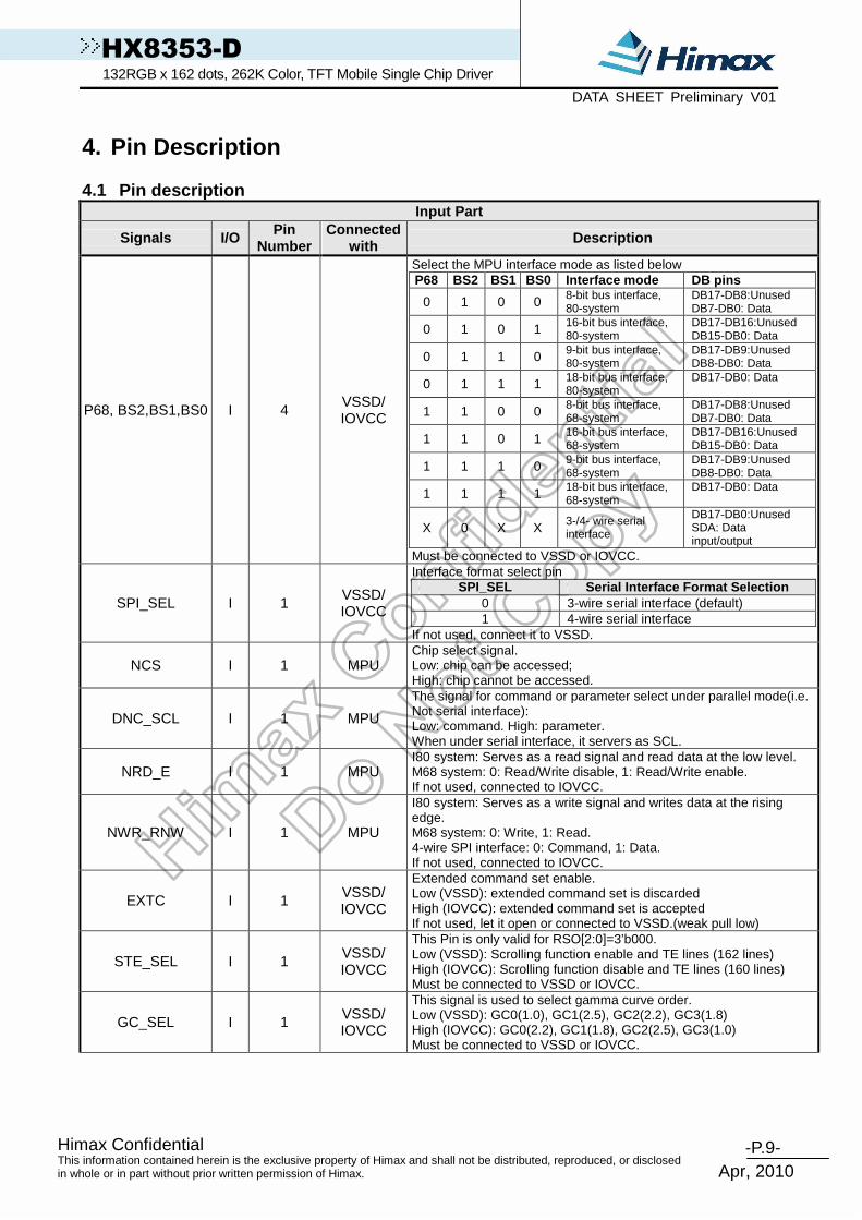
4. Pin Description 4.1 Pin description
Input Part
Signals I/O Pin Number
Connected with Description
P68, BS2,BS1,BS0 I 4 VSSD/ IOVCC
Select the MPU interface mode as listed below P68 BS2 BS1 BS0 Interface mode DB pins
0 1 0 0 8-bit bus interface, 80-system
DB17-DB8:Unused DB7-DB0: Data
0 1 0 1 16-bit bus interface, 80-system
DB17-DB16:Unused DB15-DB0: Data
0 1 1 0 9-bit bus interface, 80-system
DB17-DB9:Unused DB8-DB0: Data
0 1 1 1 18-bit bus interface, 80-system
DB17-DB0: Data
1 1 0 0 8-bit bus interface, 68-system
DB17-DB8:Unused DB7-DB0: Data
1 1 0 1 16-bit bus interface, 68-system
DB17-DB16:UnusedDB15-DB0: Data
1 1 1 0 9-bit bus interface, 68-system
DB17-DB9:Unused DB8-DB0: Data
1 1 1 1 18-bit bus interface, 68-system
DB17-DB0: Data
X 0 X X 3-/4- wire serial interface
DB17-DB0:Unused SDA: Data input/output
Must be connected to VSSD or IOVCC.
SPI_SEL I 1 VSSD/ IOVCC
Interface format select pin SPI_SEL Serial Interface Format Selection
0 3-wire serial interface (default) 1 4-wire serial interface
If not used, connect it to VSSD.
NCS I 1 MPU Chip select signal. Low: chip can be accessed; High: chip cannot be accessed.
DNC_SCL I 1 MPU
The signal for command or parameter select under parallel mode(i.e. Not serial interface): Low: command. High: parameter. When under serial interface, it servers as SCL.
NRD_E I 1 MPU I80 system: Serves as a read signal and read data at the low level. M68 system: 0: Read/Write disable, 1: Read/Write enable. If not used, connected to IOVCC.
NWR_RNW I 1 MPU
I80 system: Serves as a write signal and writes data at the rising edge. M68 system: 0: Write, 1: Read. 4-wire SPI interface: 0: Command, 1: Data. If not used, connected to IOVCC.
EXTC I 1 VSSD/ IOVCC
Extended command set enable. Low (VSSD): extended command set is discarded High (IOVCC): extended command set is accepted If not used, let it open or connected to VSSD.(weak pull low)
STE_SEL I 1 VSSD/ IOVCC
This Pin is only valid for RSO[2:0]=3’b000. Low (VSSD): Scrolling function enable and TE lines (162 lines) High (IOVCC): Scrolling function disable and TE lines (160 lines) Must be connected to VSSD or IOVCC.
GC_SEL I 1 VSSD/ IOVCC
This signal is used to select gamma curve order. Low (VSSD): GC0(1.0), GC1(2.5), GC2(2.2), GC3(1.8) High (IOVCC): GC0(2.2), GC1(1.8), GC2(2.5), GC3(1.0) Must be connected to VSSD or IOVCC.

-P.10- Himax Confidential
Apr, 2010
This information contained herein is the exclusive property of Himax and shall not be distributed, reproduced, or disclosed in whole or in part without prior written permission of Himax.
HX8353-D 132RGB x 162 dots, 262K Color, TFT Mobile Single Chip Driver DATA SHEET Preliminary V01
Input Part
Signals I/O Pin Number
Connected with Description
LC_SEL0~1 I 2 VSSD/ IOVCC
The selection pins of different liquid crystal type. Must be connected to VSSD or IOVCC.
LC_SEL1 LC_SEL0 Different liquid crystal type Selection
0 0 LC type 1 0 1 LC type 2 1 0 LC type 3 1 1 LC type 4
RSO0~2 I 3 VSSD/ IOVCC
Resolution selection pins. RSO[2:0] is used for selecting resolution. Must be connected to VSSD or IOVCC. RSO2 RSO1 RSO0 Resolution
0 0 0
GRAM resolution (Size): 132RGBX162 Display resolution: Type1 :132RGBx162 (S1~S396 and G1~G162) Type2 :128RGBx160 (S7~S390 and G2~G161)
0 0 1 GRAM resolution (Size): 128RGBx128 Display resolution: 128RGBx128 (S7~S390 and G2~G129)
0 1 0 GRAM resolution (Size): 120RGBx160 Display resolution: 120RGBx160 (S7~S366, G2~G161)
0 1 1 GRAM resolution (Size): 128RGBx160 Display resolution: 128RGBx160 (S7~S390 and G2~G161)
1 0 0 GRAM resolution: 96RGBx68 Display resolution: 96RGBx68 (S55~S342, G1~G68)
1 0 1 GRAM resolution: 96RGBx64 Display resolution: 96RGBx64 (S55~S342, G1~G64)
1 1 0 Setting disable 1 1 1 Setting disable
NRESET I 1 MPU or reset circuit
Reset pin. Setting this pin low initializes the LSI. Must be reset after power is supplied.
SS_PANEL I 1 VSSD/ IOVCC
Input pin to select the source driver scan direction on panel module. Must be connected to VSSD or IOVCC.
Module source output direction
SS_PANEL RSO[2:0] =3’b100, 3’b101
RSO[2:0] =3’b010
RSO[2:0] =3’b000 (type2),
3’b001, 3’b011
RSO[2:0] =3’b000 (type1)
0 S55 -> S342 S7 -> S366 S7 -> S390 S1 ->
S396
1 S342 -> S55
S366 -> S7 S390 -> S7 S396 -> S1
GS_PANEL I 1 VSSD/ IOVCC
Input pin to select the Gate driver scan direction on panel module. Must be connected to VSSD or IOVCC.
Module Gate output direction
GS_PANEL RSO[2:0]
=3’b101 RSO[2:0] =3’b100
RSO[2:0] =3’b000 (type2), 3’b010, 3’b011
RSO[2:0] =3’b001
RSO[2:0] =3’b000 (type1)
0 G1 -> G64
G1 -> G68
G2 -> G161
G2 -> G129
G1 -> G162
1 G64 -> G1
G68 -> G1
G161 -> G2
G129 -> G2
G162 -> G1

-P.11- Himax Confidential
Apr, 2010
This information contained herein is the exclusive property of Himax and shall not be distributed, reproduced, or disclosed in whole or in part without prior written permission of Himax.
HX8353-D 132RGB x 162 dots, 262K Color, TFT Mobile Single Chip Driver DATA SHEET Preliminary V01
Input Part
Signals I/O Pin Number
Connected with Description
REV_PANEL I 1 VSSD/ IOVCC
Input pin to select the display reversion. Must be connected to VSSD or IOVCC.
REV_PANEL Mapping data
0 “0” to maximum pixel voltage for normal white panel
1 “0” to minimum pixel voltage for normal black panel
BGR_PANEL I 1 VSSD/ IOVCC
Input pin to select the color mapping. Must be connected to VSSD or IOVCC.
BGR_PANEL Color mapping 0 S1、S2、S3 filter order = R → G → B 1 S1、S2、S3 filter order = B → G → R
TEST2-1 I 2 VSSD Test pins. Let it open or connected to VSSD. (weak pull low)
OSC I 1 Open or
Connect to VSSD
Oscillator input for test purpose. If not used, please let it open or connected to VSSD.
Output Part
Signals I/O Pin Number
Connected with Description
S1~396 O 396 LCD
Output voltages applied to the liquid crystal. SS=0, ram address “0000” is output from S1. SS=1, ram address “0000” is output from S396. S1,S2,S3 =’R’,’G’,’B’ (SS=0, BGR=0).
G1~162 O 162 LCD Output signals from gate lines. VGH: the level to select the gate lines VGL: the level not to select the gate lines
VCOM O 3 TFT
common electrode
The power supply of common voltage in TFT driving. The voltage amplitude between VCOMH and VCOML is output. The alternation cycle can be set by the POL pin. Connect this pin to the common electrode in TFT panel.
VCOMH O 3 Open This pin indicates a high level of VCOM amplitude generated in driving the VCOM alternation. Let it open.
VCOML O 3 Open When the VCOM alternation is driven, this pin indicates a low level of VCOM amplitude. When the VCOMG bit is low, the VCOML output stops. Let it open.
VREG1 O 3 Open Internal generated stable power for source driver. Let it open.
DDVDH O 5 Stabilizing capacitor
An output from the step-up circuit1, of twice the VCI level. Connect to a stabilizing capacitor between VSSA and DDVDH.
VGH O 3 Open The step-up rate is determined with BT2-0 bits. Let it open.
VGL O 3 Stabilizing capacitor
The step-up rate is determined with BT2-0 bits. Connect to a stabilizing capacitor between VSSA and VGL.
VCL O 3 Open An output from the step-up circuit1. A negative voltage for VCOML circuit, VCL= -VCI. Let it open.
TE O 1 MPU or
open
A frame start pulse output (amplitude: IOVCC-VSSD). Use when writing data to RAM in synchronization with FLM. When FLM is not used, disconnect it
VTESTOUT O 1 Open A test pin. Disconnect it.
VDDD O 3 Open Output from internal logic voltage. Let it open.
VBGP O 3 Open Reference voltage for power circuit. Let it open.
TS7~0 O 8 Open Test pins. Let these pins open.

-P.12- Himax Confidential
Apr, 2010
This information contained herein is the exclusive property of Himax and shall not be distributed, reproduced, or disclosed in whole or in part without prior written permission of Himax.
HX8353-D 132RGB x 162 dots, 262K Color, TFT Mobile Single Chip Driver DATA SHEET Preliminary V01
Input/Output Part
Signals I/O Pin Number
Connected with Description
C11A,C11B I/O 4,4 Stabilizing capacitor
Connect a pump capacitor between C11A and C11B.
Dummy35 ~ 40 I/O 3,3 Open Dummy pads. Please open these pins.
Dummy23 ~ 34 I/O 3,3 3,3
Open Dummy pads. Please open these pins.
DB0_SDA DB1~17 I/O 18 MPU
When Operates in system interface mode, it is used liked an 18-bit bi-directional data bus. 8-bit bus: use DB7-DB0 9-bit bus: use DB8-DB0 16-bit bus: use DB15-DB0 18-bit bus: use DB17-DB0 For serial interface, this pin (SDA) is for serial data pin when operate on serial data transfer interface mode of Command-parameter Interface mode. Data would be latched on the rising edge of the SCL signal. Let unused data pins open or pulled Gnd or pulled IOVCC.
DUMMY - 39 Open Dummy pads. Disconnect them.
DUMMYR1~R2 - 2 - Dummy pads. Available for measuring the COG contact resistance. DUMMYR1 and DUMMYR2 are short-circuited within the chip.
Power Part
Signals I/O Pin Number
Connected with Description
IOVCC P 17 Power supply
Power supply for interface pin. IOVCC = 1.65 ~3.3 V.
VSSD P 17 Power supply
Ground for the logic side. VSSD = 0V
VSSA P 9 Power supply
Analog ground. VSSA = 0V. When using the COG method, connect to VSSD on the FPC to prevent noise.
VCI P 6 Power supply
A power supply for the analog circuit. VCI = 2.5 ~ 3.3V

-P.13- Himax Confidential
Apr, 2010
This information contained herein is the exclusive property of Himax and shall not be distributed, reproduced, or disclosed in whole or in part without prior written permission of Himax.
HX8353-D 132RGB x 162 dots, 262K Color, TFT Mobile Single Chip Driver DATA SHEET Preliminary V01
4.2 Pin assignment
Chip size : 9900um x 675um
Chip thickness : 250um(typ.)/350um
Pad coordinate : PAD center
Coordinate Origin : Chip Center
Numbers in the figure corresponds to
pad coordinate numbers
Alignment Mark
Arrangement : Two places
Au Bump Size
TS7
Y
X
HX8353-D
Pin Assignment
(Bump View)
FACE UP
NO.1
Au bump height : 12um +/- 3um
IOVCC
EXTC
VSSD
IOVCC
BS1
VSSD
P68
IOVCC
DUMMY
DUMMY
VSSD
DUMMY
VSSD
GS_ PANEL
IOVCC
SS_ PANEL
VSSD
BGR_ PANEL
IOVCC
DUMMY
VSSD
DUMMY
IOVCC
DUMMY
VSSD
REV_ PANEL
IOVCC
GC_SEL
DUMMY
RSO0
IOVCC
RSO1
VSSD
RSO2
IOVCC
LC_SEL1
VSSD
LC_SEL0
IOVCC
TS5
TS6
IOVCC
SPI_SEL
TS3
VCI
OSC
TEST1
VCI
VCI
STE_SEL
VSSA
VSSA
VSSA
VSSA
VSSA
VSSA
DB11
DB12
DB13
DB14
DB15
DB16
NRD_E
DDVDH
DDVDH
DDVDH
VTESTOUT
TEST2
VBGP
VBGP
VBGP
DB7
C11A
C11A
C11A
DUMMYR2
VREG1
VREG1
VREG1
DDVDH
DDVDH
VCL
VCL
VCL
VSSA
VSSA
VSSA
DUMMY
DYMMY
C11B
C11B
C11B
C11B
C11A
VCOM
VCOM
VCOM
VCOMH
VCOMH
VCOMH
VGH
VSSD
TS4
NO.186
VSSD
DB17
DUMMY
BS0
DNC_SCL
TE
DB4
DB2
DUMMY
VSSD
VSSD
IOVCC
IOVCC
VDDD
DUMMY
DUMMY
DUMMY
DUMMYR1
DUMMY
DUMMY
G4
G2
DUMMY
DUMMY
DUMMY
DUMMY
S396
S395
S200
S199
DUMMY
DUMMY
DUMMY
DUMMY
DUMMY
DUMMY
S1
S2
DUMMY
DUMMY
G1
G3
G159
G161
DUMMY
DUMMY
NO.97
NO.102
NO.138
NO.145
NO.185
NO.267
NO.469
NO.671
NO.756
Including : Seal-ring : 4um * 2
Scribe line : 40um * 2
VDDD
VDDD
S198
S197
DB5
DB3
DB1
DB8
DB9
DB10
NRESET
NCS
DB6
DUMMY
DUMMY
DB0_SDA
NWR_RNW
DUMMY
TS2
TS1
TS0
NO.108
VGL
VGH
VGL
VGL
VGH
VCOML
VCOML
VCOML
BS2
G162
G160
NO.274
NO.678
NO.472
NO.473
NO.476
Bump height tolerance +/- 3um
Bump size tolerance :
Output bump width : 16 +/- 2um
Output bump length : 98 +/- 3um
Input bump width : 35/40 +/- 3um
Input bump length : 90 +/- 3um VCI
VCI
VCI
A1
A2
A1 : Coordinate(X,Y)=(-4841,-220)
A2 : Coordinate(X,Y)=(4841,-220)
DUMMY
DUMMY

-P.14- Himax Confidential
Apr, 2010
This information contained herein is the exclusive property of Himax and shall not be distributed, reproduced, or disclosed in whole or in part without prior written permission of Himax.
HX8353-D 132RGB x 162 dots, 262K Color, TFT Mobile Single Chip Driver DATA SHEET Preliminary V01
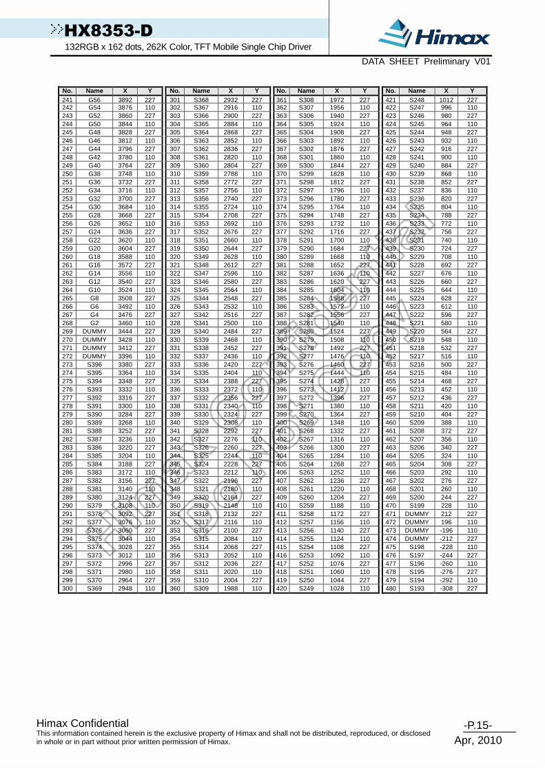
4.3 PAD coordinates
No. Name X Y No. Name X Y No. Name X Y No. Name X Y 1 TS7 -4750 -231 -
261 VSSA -1750 -231 121 DDVDH 1550 -231 181 VCOML 4550 -231
2 IOVCC -4700 -231 -2
62 VSSA -1700 -231 122 DDVDH 1600 -231 182 VCOM 4600 -231 3 EXTC -4650 -231 -
263 NRD_E -1630 -231 123 DDVDH 1650 -231 183 VCOM 4650 -231
4 VSSD -4600 -231 -2
64 DNC_SCL -1570 -231 124 DDVDH 1700 -231 184 VCOM 4700 -231 5 BS0 -4550 -231 -
265 STE_SEL -1510 -231 125 VREG1 1750 -231 185 DUMMY 4750 -231
6 IOVCC -4500 -231 -2
66 VSSD -1450 -231 126 VREG1 1800 -231 186 DUMMY 4772 110 7 BS1 -4450 -231 -
267 DB17 -1390 -231 127 VREG1 1850 -231 187 DUMMY 4756 227
8 VSSD -4400 -231 -2
68 DB16 -1330 -231 128 DUMMYR1 1900 -231 188 G162 4740 110 9 P68 -4350 -231 -
269 DB15 -1270 -231 129 DUMMYR2 1950 -231 189 G160 4724 227
10 IOVCC -4300 -231 -2
70 DB14 -1210 -231 130 C11A 2000 -231 190 G158 4708 110 11 DUMMY -4250 -231 -
271 DB13 -1150 -231 131 C11A 2050 -231 191 G156 4692 227
12 VSSD -4200 -231 -2
72 DB12 -1090 -231 132 C11A 2100 -231 192 G154 4676 110 13 DUMMY -4150 -231 -
273 DB11 -1030 -231 133 C11A 2150 -231 193 G152 4660 227
14 IOVCC -4100 -231 -2
74 DB10 -970 -231 134 C11B 2200 -231 194 G150 4644 110 15 BGR_PANEL -4050 -231 -
275 DB9 -910 -231 135 C11B 2250 -231 195 G148 4628 227
16 VSSD -4000 -231 -2
76 DB8 -850 -231 136 C11B 2300 -231 196 G146 4612 110 17 SS_PANEL -3950 -231 -
277 DB1 -790 -231 137 C11B 2350 -231 197 G144 4596 227
18 IOVCC -3900 -231 -2
78 DB3 -730 -231 138 DUMMY 2400 -231 198 G142 4580 110 19 GS_PANEL -3850 -231 -
279 DB5 -670 -231 139 DUMMY 2450 -231 199 G140 4564 227
20 VSSD -3800 -231 -2
80 DB7 -610 -231 140 DUMMY 2500 -231 200 G138 4548 110 21 DUMMY -3750 -231 -
281 TE -550 -231 141 DUMMY 2550 -231 201 G136 4532 227
22 IOVCC -3700 -231 -2
82 NRESET -490 -231 142 DUMMY 2600 -231 202 G134 4516 110 23 REV_PANEL -3650 -231 -
283 NCS -430 -231 143 DUMMY 2650 -231 203 G132 4500 227
24 VSSD -3600 -231 -2
84 DB6 -370 -231 144 DUMMY 2700 -231 204 G130 4484 110 25 DUMMY -3550 -231 -
285 DB4 -310 -231 145 DUMMY 2750 -231 205 G128 4468 227
26 IOVCC -3500 -231 -2
86 DB2 -250 -231 146 VSSA 2800 -231 206 G126 4452 110 27 DUMMY -3450 -231 -
287 BS2 -190 -231 147 VSSA 2850 -231 207 G124 4436 227
28 VSSD -3400 -231 -2
88 DB0_SDA -130 -231 148 VSSA 2900 -231 208 G122 4420 110 29 DUMMY -3350 -231 -
289 NWR_RNW -70 -231 149 VCL 2950 -231 209 G120 4404 227
30 IOVCC -3300 -231 -2
90 DUMMY 0 -231 150 VCL 3000 -231 210 G118 4388 110 31 LC_SEL0 -3250 -231 -
291 DUMMY 50 -231 151 VCL 3050 -231 211 G116 4372 227
32 VSSD -3200 -231 -2
92 DUMMY 100 -231 152 DUMMY23 3100 -231 212 G114 4356 110 33 LC_SEL1 -3150 -231 -
293 DUMMY 150 -231 153 DUMMY24 3150 -231 213 G112 4340 227
34 IOVCC -3100 -231 -2
94 TS2 200 -231 154 DUMMY25 3200 -231 214 G110 4324 110 35 RSO2 -3050 -231 -
295 TS1 250 -231 155 DUMMY26 3250 -231 215 G108 4308 227
36 VSSD -3000 -231 -2
96 TS0 300 -231 156 DUMMY27 3300 -231 216 G106 4292 110 37 RSO1 -2950 -231 -
297 VSSD 350 -231 157 DUMMY28 3350 -231 217 G104 4276 227
38 IOVCC -2900 -231 -2
98 VSSD 400 -231 158 DUMMY29 3400 -231 218 G102 4260 110 39 RSO0 -2850 -231 -
299 VSSD 450 -231 159 DUMMY30 3450 -231 219 G100 4244 227
40 VSSD -2800 -231 -2
100 VSSD 500 -231 160 DUMMY31 3500 -231 220 G98 4228 110 41 DUMMY -2750 -231 -
2101 VSSD 550 -231 161 DUMMY32 3550 -231 221 G96 4212 227
42 GC_SEL -2700 -231 -2
102 VSSD 600 -231 162 DUMMY33 3600 -231 222 G94 4196 110 43 SPI_SEL -2650 -231 -
2103 IOVCC 650 -231 163 DUMMY34 3650 -231 223 G92 4180 227
44 IOVCC -2600 -231 -2
104 IOVCC 700 -231 164 DUMMY35 3700 -231 224 G90 4164 110 45 TS6 -2550 -231 -
2105 IOVCC 750 -231 165 DUMMY36 3750 -231 225 G88 4148 227
46 TS5 -2500 -231 -2
106 IOVCC 800 -231 166 DUMMY37 3800 -231 226 G86 4132 110 47 TS4 -2450 -231 -
2107 IOVCC 850 -231 167 DUMMY38 3850 -231 227 G84 4116 227
48 TS3 -2400 -231 -2
108 IOVCC 900 -231 168 DUMMY39 3900 -231 228 G82 4100 110 49 TEST1 -2350 -231 -
2109 VDDD 950 -231 169 DUMMY40 3950 -231 229 G80 4084 227
50 OSC -2300 -231 -2
110 VDDD 1000 -231 170 VGL 4000 -231 230 G78 4068 110 51 VCI -2250 -231 -
2111 VDDD 1050 -231 171 VGL 4050 -231 231 G76 4052 227
52 VCI -2200 -231 -2
112 DUMMY 1100 -231 172 VGL 4100 -231 232 G74 4036 110 53 VCI -2150 -231 -
2113 DUMMY 1150 -231 173 VGH 4150 -231 233 G72 4020 227
54 VCI -2100 -231 -2
114 DUMMY 1200 -231 174 VGH 4200 -231 234 G70 4004 110 55 VCI -2050 -231 -
2115 VBGP 1250 -231 175 VGH 4250 -231 235 G68 3988 227
56 VCI -2000 -231 -2
116 VBGP 1300 -231 176 VCOMH 4300 -231 236 G66 3972 110 57 VSSA -1950 -231 -
2117 VBGP 1350 -231 177 VCOMH 4350 -231 237 G64 3956 227
58 VSSA -1900 -231 -2
118 TEST2 1400 -231 178 VCOMH 4400 -231 238 G62 3940 110 59 VSSA -1850 -231 -
2119 VTESTOUT 1450 -231 179 VCOML 4450 -231
239 G60 3924 227
60 VSSA -1800 -231 -2
120 DDVDH 1500 -231 180 VCOML 4500 -231 240 G58 3908 110
-P.15- Himax Confidential
Apr, 2010
This information contained herein is the exclusive property of Himax and shall not be distributed, reproduced, or disclosed in whole or in part without prior written permission of Himax.
HX8353-D 132RGB x 162 dots, 262K Color, TFT Mobile Single Chip Driver DATA SHEET Preliminary V01
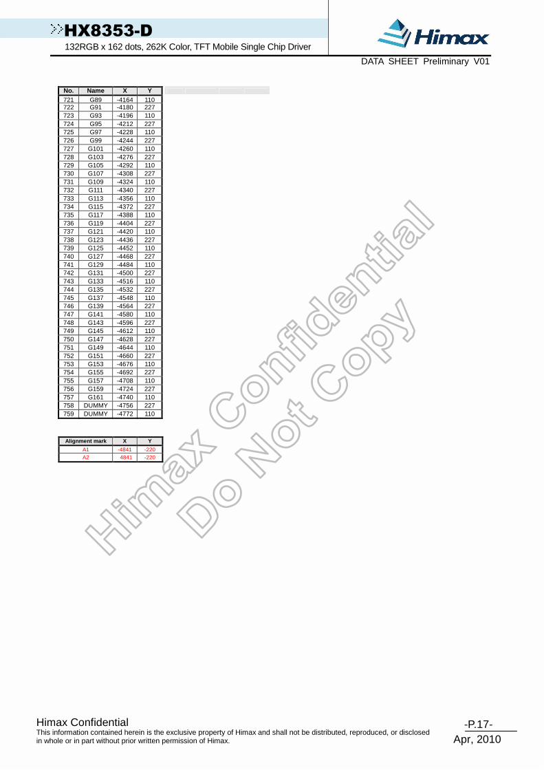
No. Name X Y No. Name X Y No. Name X Y No. Name X Y 241 G56 3892 227 301 S368 2932 227 361 S308 1972 227 421 S248 1012 227 242 G54 3876 110 302 S367 2916 110 362 S307 1956 110 422 S247 996 110 243 G52 3860 227 303 S366 2900 227 363 S306 1940 227 423 S246 980 227 244 G50 3844 110 304 S365 2884 110 364 S305 1924 110 424 S245 964 110 245 G48 3828 227 305 S364 2868 227 365 S304 1908 227 425 S244 948 227 246 G46 3812 110 306 S363 2852 110 366 S303 1892 110 426 S243 932 110 247 G44 3796 227 307 S362 2836 227 367 S302 1876 227 427 S242 916 227 248 G42 3780 110 308 S361 2820 110 368 S301 1860 110 428 S241 900 110 249 G40 3764 227 309 S360 2804 227 369 S300 1844 227 429 S240 884 227 250 G38 3748 110 310 S359 2788 110 370 S299 1828 110 430 S239 868 110 251 G36 3732 227 311 S358 2772 227 371 S298 1812 227 431 S238 852 227 252 G34 3716 110 312 S357 2756 110 372 S297 1796 110 432 S237 836 110 253 G32 3700 227 313 S356 2740 227 373 S296 1780 227 433 S236 820 227 254 G30 3684 110 314 S355 2724 110 374 S295 1764 110 434 S235 804 110 255 G28 3668 227 315 S354 2708 227 375 S294 1748 227 435 S234 788 227 256 G26 3652 110 316 S353 2692 110 376 S293 1732 110 436 S233 772 110 257 G24 3636 227 317 S352 2676 227 377 S292 1716 227 437 S232 756 227 258 G22 3620 110 318 S351 2660 110 378 S291 1700 110 438 S231 740 110 259 G20 3604 227 319 S350 2644 227 379 S290 1684 227 439 S230 724 227 260 G18 3588 110 320 S349 2628 110 380 S289 1668 110 440 S229 708 110 261 G16 3572 227 321 S348 2612 227 381 S288 1652 227 441 S228 692 227 262 G14 3556 110 322 S347 2596 110 382 S287 1636 110 442 S227 676 110 263 G12 3540 227 323 S346 2580 227 383 S286 1620 227 443 S226 660 227 264 G10 3524 110 324 S345 2564 110 384 S285 1604 110 444 S225 644 110 265 G8 3508 227 325 S344 2548 227 385 S284 1588 227 445 S224 628 227 266 G6 3492 110 326 S343 2532 110 386 S283 1572 110 446 S223 612 110 267 G4 3476 227 327 S342 2516 227 387 S282 1556 227 447 S222 596 227 268 G2 3460 110 328 S341 2500 110 388 S281 1540 110 448 S221 580 110 269 DUMMY 3444 227 329 S340 2484 227 389 S280 1524 227 449 S220 564 227 270 DUMMY 3428 110 330 S339 2468 110 390 S279 1508 110 450 S219 548 110 271 DUMMY 3412 227 331 S338 2452 227 391 S278 1492 227 451 S218 532 227 272 DUMMY 3396 110 332 S337 2436 110 392 S277 1476 110 452 S217 516 110 273 S396 3380 227 333 S336 2420 227 393 S276 1460 227 453 S216 500 227 274 S395 3364 110 334 S335 2404 110 394 S275 1444 110 454 S215 484 110 275 S394 3348 227 335 S334 2388 227 395 S274 1428 227 455 S214 468 227 276 S393 3332 110 336 S333 2372 110 396 S273 1412 110 456 S213 452 110 277 S392 3316 227 337 S332 2356 227 397 S272 1396 227 457 S212 436 227 278 S391 3300 110 338 S331 2340 110 398 S271 1380 110 458 S211 420 110 279 S390 3284 227 339 S330 2324 227 399 S270 1364 227 459 S210 404 227 280 S389 3268 110 340 S329 2308 110 400 S269 1348 110 460 S209 388 110 281 S388 3252 227 341 S328 2292 227 401 S268 1332 227 461 S208 372 227 282 S387 3236 110 342 S327 2276 110 402 S267 1316 110 462 S207 356 110 283 S386 3220 227 343 S326 2260 227 403 S266 1300 227 463 S206 340 227 284 S385 3204 110 344 S325 2244 110 404 S265 1284 110 464 S205 324 110 285 S384 3188 227 345 S324 2228 227 405 S264 1268 227 465 S204 308 227 286 S383 3172 110 346 S323 2212 110 406 S263 1252 110 466 S203 292 110 287 S382 3156 227 347 S322 2196 227 407 S262 1236 227 467 S202 276 227 288 S381 3140 110 348 S321 2180 110 408 S261 1220 110 468 S201 260 110 289 S380 3124 227 349 S320 2164 227 409 S260 1204 227 469 S200 244 227 290 S379 3108 110 350 S319 2148 110 410 S259 1188 110 470 S199 228 110 291 S378 3092 227 351 S318 2132 227 411 S258 1172 227 471 DUMMY 212 227 292 S377 3076 110 352 S317 2116 110 412 S257 1156 110 472 DUMMY 196 110 293 S376 3060 227 353 S316 2100 227 413 S256 1140 227 473 DUMMY -196 110 294 S375 3044 110 354 S315 2084 110 414 S255 1124 110 474 DUMMY -212 227 295 S374 3028 227 355 S314 2068 227 415 S254 1108 227 475 S198 -228 110 296 S373 3012 110 356 S313 2052 110 416 S253 1092 110 476 S197 -244 227 297 S372 2996 227 357 S312 2036 227 417 S252 1076 227 477 S196 -260 110 298 S371 2980 110 358 S311 2020 110 418 S251 1060 110 478 S195 -276 227 299 S370 2964 227 359 S310 2004 227 419 S250 1044 227
479 S194 -292 110
300 S369 2948 110 360 S309 1988 110 420 S249 1028 110 480 S193 -308 227

-P.16- Himax Confidential
Apr, 2010
This information contained herein is the exclusive property of Himax and shall not be distributed, reproduced, or disclosed in whole or in part without prior written permission of Himax.
HX8353-D 132RGB x 162 dots, 262K Color, TFT Mobile Single Chip Driver DATA SHEET Preliminary V01
No. Name X Y No. Name X Y No. Name X Y No. Name X Y 481 S192 -324 110 541 S132 -1284 110 601 S72 -2244 110 661 S12 -3204 110 482 S191 -340 227 542 S131 -1300 227 602 S71 -2260 227 662 S11 -3220 227 483 S190 -356 110 543 S130 -1316 110 603 S70 -2276 110 663 S10 -3236 110 484 S189 -372 227 544 S129 -1332 227 604 S69 -2292 227 664 S9 -3252 227 485 S188 -388 110 545 S128 -1348 110 605 S68 -2308 110 665 S8 -3268 110 486 S187 -404 227 546 S127 -1364 227 606 S67 -2324 227 666 S7 -3284 227 487 S186 -420 110 547 S126 -1380 110 607 S66 -2340 110 667 S6 -3300 110 488 S185 -436 227 548 S125 -1396 227 608 S65 -2356 227 668 S5 -3316 227 489 S184 -452 110 549 S124 -1412 110 609 S64 -2372 110 669 S4 -3332 110 490 S183 -468 227 550 S123 -1428 227 610 S63 -2388 227 670 S3 -3348 227 491 S182 -484 110 551 S122 -1444 110 611 S62 -2404 110 671 S2 -3364 110 492 S181 -500 227 552 S121 -1460 227 612 S61 -2420 227 672 S1 -3380 227 493 S180 -516 110 553 S120 -1476 110 613 S60 -2436 110 673 DUMMY -3396 110 494 S179 -532 227 554 S119 -1492 227 614 S59 -2452 227 674 DUMMY -3412 227 495 S178 -548 110 555 S118 -1508 110 615 S58 -2468 110 675 DUMMY -3428 110 496 S177 -564 227 556 S117 -1524 227 616 S57 -2484 227 676 DUMMY -3444 227 497 S176 -580 110 557 S116 -1540 110 617 S56 -2500 110 677 G1 -3460 110 498 S175 -596 227 558 S115 -1556 227 618 S55 -2516 227 678 G3 -3476 227 499 S174 -612 110 559 S114 -1572 110 619 S54 -2532 110 679 G5 -3492 110 500 S173 -628 227 560 S113 -1588 227 620 S53 -2548 227 680 G7 -3508 227 501 S172 -644 110 561 S112 -1604 110 621 S52 -2564 110 681 G9 -3524 110 502 S171 -660 227 562 S111 -1620 227 622 S51 -2580 227 682 G11 -3540 227 503 S170 -676 110 563 S110 -1636 110 623 S50 -2596 110 683 G13 -3556 110 504 S169 -692 227 564 S109 -1652 227 624 S49 -2612 227 684 G15 -3572 227 505 S168 -708 110 565 S108 -1668 110 625 S48 -2628 110 685 G17 -3588 110 506 S167 -724 227 566 S107 -1684 227 626 S47 -2644 227 686 G19 -3604 227 507 S166 -740 110 567 S106 -1700 110 627 S46 -2660 110 687 G21 -3620 110 508 S165 -756 227 568 S105 -1716 227 628 S45 -2676 227 688 G23 -3636 227 509 S164 -772 110 569 S104 -1732 110 629 S44 -2692 110 689 G25 -3652 110 510 S163 -788 227 570 S103 -1748 227 630 S43 -2708 227 690 G27 -3668 227 511 S162 -804 110 571 S102 -1764 110 631 S42 -2724 110 691 G29 -3684 110 512 S161 -820 227 572 S101 -1780 227 632 S41 -2740 227 692 G31 -3700 227 513 S160 -836 110 573 S100 -1796 110 633 S40 -2756 110 693 G33 -3716 110 514 S159 -852 227 574 S99 -1812 227 634 S39 -2772 227 694 G35 -3732 227 515 S158 -868 110 575 S98 -1828 110 635 S38 -2788 110 695 G37 -3748 110 516 S157 -884 227 576 S97 -1844 227 636 S37 -2804 227 696 G39 -3764 227 517 S156 -900 110 577 S96 -1860 110 637 S36 -2820 110 697 G41 -3780 110 518 S155 -916 227 578 S95 -1876 227 638 S35 -2836 227 698 G43 -3796 227 519 S154 -932 110 579 S94 -1892 110 639 S34 -2852 110 699 G45 -3812 110 520 S153 -948 227 580 S93 -1908 227 640 S33 -2868 227 700 G47 -3828 227 521 S152 -964 110 581 S92 -1924 110 641 S32 -2884 110 701 G49 -3844 110 522 S151 -980 227 582 S91 -1940 227 642 S31 -2900 227 702 G51 -3860 227 523 S150 -996 110 583 S90 -1956 110 643 S30 -2916 110 703 G53 -3876 110 524 S149 -1012 227 584 S89 -1972 227 644 S29 -2932 227 704 G55 -3892 227 525 S148 -1028 110 585 S88 -1988 110 645 S28 -2948 110 705 G57 -3908 110 526 S147 -1044 227 586 S87 -2004 227 646 S27 -2964 227 706 G59 -3924 227 527 S146 -1060 110 587 S86 -2020 110 647 S26 -2980 110 707 G61 -3940 110 528 S145 -1076 227 588 S85 -2036 227 648 S25 -2996 227 708 G63 -3956 227 529 S144 -1092 110 589 S84 -2052 110 649 S24 -3012 110 709 G65 -3972 110 530 S143 -1108 227 590 S83 -2068 227 650 S23 -3028 227 710 G67 -3988 227 531 S142 -1124 110 591 S82 -2084 110 651 S22 -3044 110 711 G69 -4004 110 532 S141 -1140 227 592 S81 -2100 227 652 S21 -3060 227 712 G71 -4020 227 533 S140 -1156 110 593 S80 -2116 110 653 S20 -3076 110 713 G73 -4036 110 534 S139 -1172 227 594 S79 -2132 227 654 S19 -3092 227 714 G75 -4052 227 535 S138 -1188 110 595 S78 -2148 110 655 S18 -3108 110 715 G77 -4068 110 536 S137 -1204 227 596 S77 -2164 227 656 S17 -3124 227 716 G79 -4084 227 537 S136 -1220 110 597 S76 -2180 110 657 S16 -3140 110 717 G81 -4100 110 538 S135 -1236 227 598 S75 -2196 227 658 S15 -3156 227 718 G83 -4116 227 539 S134 -1252 110 599 S74 -2212 110 659 S14 -3172 110
719 G85 -4132 110
540 S133 -1268 227 600 S73 -2228 227 660 S13 -3188 227 720 G87 -4148 227
-P.17- Himax Confidential
Apr, 2010
This information contained herein is the exclusive property of Himax and shall not be distributed, reproduced, or disclosed in whole or in part without prior written permission of Himax.
HX8353-D 132RGB x 162 dots, 262K Color, TFT Mobile Single Chip Driver DATA SHEET Preliminary V01
No. Name X Y
721 G89 -4164 110 722 G91 -4180 227 723 G93 -4196 110 724 G95 -4212 227 725 G97 -4228 110 726 G99 -4244 227 727 G101 -4260 110 728 G103 -4276 227 729 G105 -4292 110 730 G107 -4308 227 731 G109 -4324 110 732 G111 -4340 227 733 G113 -4356 110 734 G115 -4372 227 735 G117 -4388 110 736 G119 -4404 227 737 G121 -4420 110 738 G123 -4436 227 739 G125 -4452 110 740 G127 -4468 227 741 G129 -4484 110 742 G131 -4500 227 743 G133 -4516 110 744 G135 -4532 227 745 G137 -4548 110 746 G139 -4564 227 747 G141 -4580 110 748 G143 -4596 227 749 G145 -4612 110 750 G147 -4628 227 751 G149 -4644 110 752 G151 -4660 227 753 G153 -4676 110 754 G155 -4692 227 755 G157 -4708 110 756 G159 -4724 227 757 G161 -4740 110 758 DUMMY -4756 227 759 DUMMY -4772 110
Alignment mark X Y
A1 -4841 -220 A2 4841 -220

-P.18- Himax Confidential
Apr, 2010
This information contained herein is the exclusive property of Himax and shall not be distributed, reproduced, or disclosed in whole or in part without prior written permission of Himax.
HX8353-D 132RGB x 162 dots, 262K Color, TFT Mobile Single Chip Driver DATA SHEET Preliminary V01
4.4 Alignment mark
A_MARK (A1)
15 um
15 um
15 um
20 um
15 um
5um10um
10 um
5 um
15um 15um 20um 15um 15um
A_MARK (A2)
15 um
15um
15 um
20um
15um
5um 10 um
10um
5um
15um15um20 um15 um15 um

-P.19- Himax Confidential
Apr, 2010
This information contained herein is the exclusive property of Himax and shall not be distributed, reproduced, or disclosed in whole or in part without prior written permission of Himax.
HX8353-D 132RGB x 162 dots, 262K Color, TFT Mobile Single Chip Driver DATA SHEET Preliminary V01
4.5 Bump size
Input/Output PAD
Note: 35µmX90µm : Pad no. 1~62 Pad no. 90~185
40µmX90µm: Pad no. 63~89
Output PAD
Note: 16µmX98µm : Pad no.186~759
35 µm X 90 µm
50µm 35µm
90µm
40 µm X90 µm
60µm 40µm
90µm
16µm
16 µm X 98 µm
19µm
32µm
98µm

-P.20- Himax Confidential
Apr, 2010
This information contained herein is the exclusive property of Himax and shall not be distributed, reproduced, or disclosed in whole or in part without prior written permission of Himax.
HX8353-D 132RGB x 162 dots, 262K Color, TFT Mobile Single Chip Driver DATA SHEET Preliminary V01
5. Interface 5.1 System interface
The HX8353-D supports parallel 80-system and 68-system 18-/16-/9-/8-bits bus interface mode and 3-/4- wires serial interface mode. When NCS = “L”, the parallel and serial bus system interface of the HX8353-D become active and data transfer through the interface circuit is available. The DNC_SCL pin specifies whether the system interface circuit access is to the register command or to the GRAM. The input bus width format of system interface circuit is selected by external pins BS2-0. For selecting the format of input bus, please refer to Table 5.1 and Table 5.2. The HX8353-D includes command code and the following parameter and GRAM data. The command code can be written through data bus by setting DNC_SCL=0. Then the command or GRAM data can be written to register at which that index pointer pointed by setting DNC_SCL=1. Furthermore, there are two 18-bit bus control registers used to temporarily store the data written to or read from the GRAM. When the data is written into the GRAM from the MPU, it is first written into the write-data latch and then automatically written into the GRAM by internal operation. Data is read through the read-data latch when reading from the GRAM. Therefore, the first read data operation is invalid and the following read data operations are valid.
SPI_SEL P68 BS2 BS1 BS0 Interface x 0 1 0 0 80-system 8-bit Parallel x 0 1 0 1 80-system 16-bit Parallel x 0 1 1 0 80-system 9-bit Parallel x 0 1 1 1 80-system 18-bit Parallel x 1 1 0 0 68-system 8-bit Parallel x 1 1 0 1 68-system 16-bit Parallel x 1 1 1 0 68-system 9-bit Parallel x 1 1 1 1 68-system 18-bit Parallel 0 x 0 x x 3 wire serial Interface only 1 x 0 x x 4 wire serial Interface only
Table 5.1 Interface selection
DB17 – DB0 Interface NRD_E NWR_RNW DNC_SCL Command/Parameter GRAM
80-system 8-bit Parallel NRD NWR DNC DB7-DB0 DB7-DB0 80-system 9-bit Parallel NRD NWR DNC DB7-DB0 DB8-DB0 80-system 16-bit Parallel NRD NWR DNC DB7-DB0 DB15-DB0 80-system 18-bit Parallel NRD NWR DNC DB7-DB0 DB17-DB0 3 wire serial Interface - - SCL DB0 as SDA 68-system 8-bit Parallel E RW DNC DB7-DB0 DB7-DB0 68-system 9-bit Parallel E RW DNC DB7-DB0 DB8-DB0 68-system 16-bit Parallel E RW DNC DB7-DB0 DB15-DB0 68-system 18-bit Parallel E RW DNC DB7-DB0 DB17-DB0 4 wire serial Interface - DNC SCL DB0 as SDA
Table 5.2 Interface mode selection
-P.21- Himax Confidential
Apr, 2010
This information contained herein is the exclusive property of Himax and shall not be distributed, reproduced, or disclosed in whole or in part without prior written permission of Himax.
HX8353-D 132RGB x 162 dots, 262K Color, TFT Mobile Single Chip Driver DATA SHEET Preliminary V01
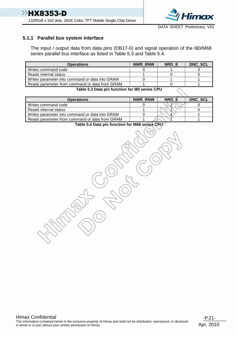
5.1.1 Parallel bus system interface
The input / output data from data pins (DB17-0) and signal operation of the I80/M68 series parallel bus interface as listed in Table 5.3 and Table 5.4.
Operations NWR_RNW NRD_E DNC_SCL
Writes command code 0 1 0 Reads internal status 1 0 0 Writes parameter into command or data into GRAM 0 1 1 Reads parameter from command or data from GRAM 1 0 1
Table 5.3 Data pin function for I80 series CPU
Operations NWR_RNW NRD_E DNC_SCL Writes command code 0 1 0 Reads internal status 1 1 0 Writes parameter into command or data into GRAM 0 1 1 Reads parameter from command or data from GRAM 1 1 1
Table 5.4 Data pin function for M68 series CPU

-P.22- Himax Confidential
Apr, 2010
This information contained herein is the exclusive property of Himax and shall not be distributed, reproduced, or disclosed in whole or in part without prior written permission of Himax.
HX8353-D 132RGB x 162 dots, 262K Color, TFT Mobile Single Chip Driver DATA SHEET Preliminary V01
Write to register Write to register Write to register Write to register
NCS
DNC_SCL
HOST DB7-0
(MPU to LCD)CMD PA1 PA1 PAn-3
NWR_RNW
CMD CMD
CMD PA1 PA1CMD CMDS
1 byte command
n byte command
PAn-1PAn-2
PAn-3 PAn-2 PA n-1
CMD: command code PA: parameter
NRD_E
Read from register Read from register Read from register Read from register
CMD CMD
CMD PA1 dummydummy CMDS
PA1
PA1
dummydummy PA1
CMD CMD
PA1 dummy
PAn-1
PA1dummy
2 byte command
2 byte command n byte command
Driver DB7-0
( LCD to MPU)
NCS
DNC_SCL
DB7-0
NWR_RNW
NRD_E
HOST DB7-0( MPU to LCD )
Driver DB7-0
( LCD to MPU)
CMD: command code PA: parameter
Hi - Z
Hi-Z
Hi-ZHi-Z
Hi-Z
PAn-2PAn-3
PAn-1PAn-2PAn-3
PAn-1PAn-2PAn-3
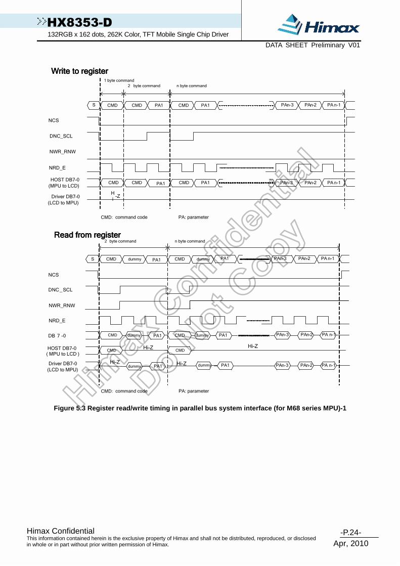
Figure 5.1 Register read/write timing in parallel b us system interface (for I80 series MPU)-1

-P.23- Himax Confidential
Apr, 2010
This information contained herein is the exclusive property of Himax and shall not be distributed, reproduced, or disclosed in whole or in part without prior written permission of Himax.
HX8353-D 132RGB x 162 dots, 262K Color, TFT Mobile Single Chip Driver DATA SHEET Preliminary V01
Write to register Write to register Write to register Write to register
NCS
DNC_SCL
HOST DB7-0
(MPU to LCD)CMD PA1
NWR_RNW
CMD
CMD PA1CMDS
1 byte command
n byte command
CMD: command code PA: parameter
NRD_E
Read from register Read from register Read from register Read from register
CMD CMD
PA1 dummyCMDS FCh
dummydummy
2 byte command
2 byte command n byte command
Driver DB7-0
( LCD to MPU)
NCS
DNC_SCL
DB7-0
NWR_RNW
NRD_E
HOST DB7-0( MPU to LCD )
Driver DB7-0
( LCD to MPU)
CMD: command code PA: parameter
Hi - Z
Hi-Z
PA1CMD PA2FDh PA n-1FDh
PA1CMD PA2FDh PA n-1FDh
PA1 FCh PA n-1FChdummyCMD
FCh PA1 FCh PA1 FCh PA n-1
CMD CMDFCh FCh FCh
Hi-Z Hi-Z Hi-Z Hi-Z
dummydummy PA1 PA1 PA n-1Hi-Z Hi-Z Hi-Z Hi-Z Hi-Z
Figure 5.2 Register read/write timing in parallel b us system interface (for I80 series MPU)-2
-P.24- Himax Confidential
Apr, 2010
This information contained herein is the exclusive property of Himax and shall not be distributed, reproduced, or disclosed in whole or in part without prior written permission of Himax.
HX8353-D 132RGB x 162 dots, 262K Color, TFT Mobile Single Chip Driver DATA SHEET Preliminary V01
Write to register Write to register Write to register Write to register
NCS
DNC_SCL
HOST DB7-0
(MPU to LCD)CMD PA1 PA1CMD CMD
CMD PA1 PA1CMD CMDS
1 byte command
n byte command
PAn-3 PAn-2 PAn-1
CMD: command code PA: parameter
NWR_RNW
H
i-Z
Read from register Read from register Read from register Read from register
CMD CMD
CMD PA1 dummydummy CMDS
PA1
PA1
dummydummy PA1
CMD CMDHi-Z
PA1 dummy PA1dummy
2 byte command
2 byte command n byte command
Driver DB7-0
(LCD to MPU)
NCS
DNC_SCL
DB 7 -0
NRD_E
NWR_RNW
HOST DB7-0( MPU to LCD )
Driver DB7-0
(LCD to MPU)
CMD: command code PA: parameter
NRD_E
Hi-Z Hi-Z
Hi-Z
PAn-3 PAn-2 PAn-1
PAn-3 PAn-2 PAn-1
PAn-3 PAn-2 PA n-1
PAn-3 PAn-2 PA n-1
Figure 5.3 Register read/write timing in parallel b us system interface (for M68 series MPU)-1
-P.25- Himax Confidential
Apr, 2010
This information contained herein is the exclusive property of Himax and shall not be distributed, reproduced, or disclosed in whole or in part without prior written permission of Himax.
HX8353-D 132RGB x 162 dots, 262K Color, TFT Mobile Single Chip Driver DATA SHEET Preliminary V01
Write to register Write to register Write to register Write to register
NCS
DNC_SCL
HOST DB7-0
(MPU to LCD)CMD PA1 PA1CMD CMD
CMD PA1 PA1CMD CMDS
1 byte command
n byte command
CMD: command code PA: parameter
NWR_RNW
H
i-Z
Read from register Read from register Read from register Read from register
2 byte command
Driver DB7-0
(LCD to MPU)
NRD_E
PA2FDh PA n-1FDh
PA2FDh PA n-1FDh
CMD CMD
PA1 dummyCMDS FCh
dummydummy
2 byte command n byte command
NCS
DNC_SCL
DB7-0
NWR_RNW
NRD_E
HOST DB7-0( MPU to LCD )
Driver DB7-0
( LCD to MPU)
CMD: command code PA: parameter
Hi-Z
PA1 FCh PA n-1FChdummyCMD
FCh PA1 FCh PA1 FCh PA n-1
CMD CMDFCh FCh FCh
Hi-Z Hi-Z Hi-Z Hi-Z
dummydummy PA1 PA1 PA n-1Hi-Z Hi-Z Hi-Z Hi-Z Hi-Z
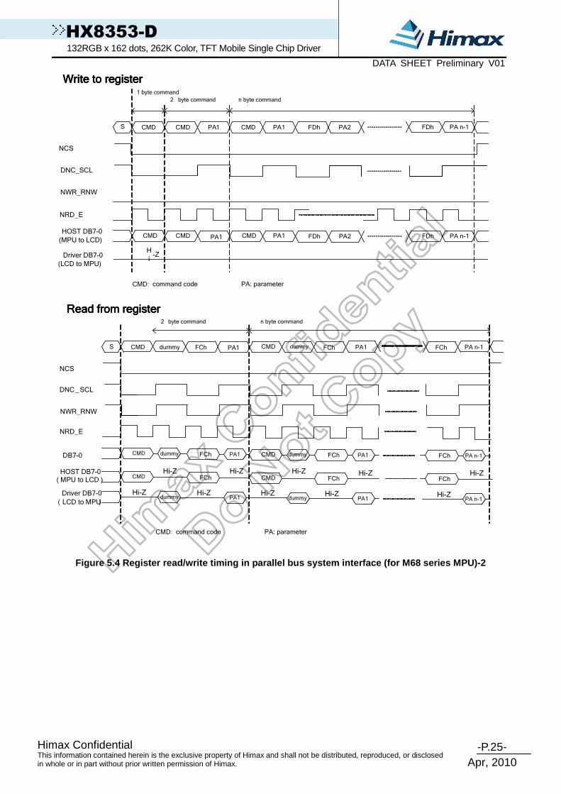
Figure 5.4 Register read/write timing in parallel b us system interface (for M68 series MPU)-2

-P.26- Himax Confidential
Apr, 2010
This information contained herein is the exclusive property of Himax and shall not be distributed, reproduced, or disclosed in whole or in part without prior written permission of Himax.
HX8353-D 132RGB x 162 dots, 262K Color, TFT Mobile Single Chip Driver DATA SHEET Preliminary V01
Write to GRAM Write to GRAM Write to GRAM Write to GRAM
NCS
DNC_SCL
(MPU to LCD)
NWR_RNW
S
CMD: command code PA: parameter
NRD_E
Read from GRAM Read from GRAM Read from GRAM Read from GRAM
S
(LCD to MPU)
NCS
DNC_SCL
NWR_WNR
NRD_E
( MPU to LCD )
(LCD to MPU)
Data 12Ch
Data 12Ch Data n-2 Data n-1 Data n
n pixel RAM data write
Data n-2 Data n-1 Data n
2Eh
dummy2Eh
Data nData n-1
Data n-2 Data n-1 Data n
dummy
Data 1
Data1
2Eh
dummy Data 1
n pixel RAM data read
Data n-2
Data nData n-1Data n-2
Hi - Z
Hi -Z
Hi -Z
Figure 5.5 GRAM read/write timing in parallel bus s ystem interface (for I80 series MPU)

-P.27- Himax Confidential
Apr, 2010
This information contained herein is the exclusive property of Himax and shall not be distributed, reproduced, or disclosed in whole or in part without prior written permission of Himax.
HX8353-D 132RGB x 162 dots, 262K Color, TFT Mobile Single Chip Driver DATA SHEET Preliminary V01
Write to GRAM Write to GRAM Write to GRAM Write to GRAM
NCS
DNC_SCL
(MPU to LCD)
NRD_E
S
CMD: command code PA: parameter
NWR_RNW
Read from GRAM Read from GRAM Read from GRAM Read from GRAM
S
(LCD to MPU)
NCS
DNC_SCL
NRD_E
NWR_RNW
( MPU to LCD )
(LCD to MPU)
:
Data 12Ch
Data 12Ch Data n-2 Data n-1 Data n
n pixel RAM data write
Data n-2 Data n-1 Data n
2Eh
dummy2Eh
Data nData n-1
Data n-2 Data n-1 Data n
dummy
Data 1
Data1
2Eh
dummy Data 1
n pixel RAM data read
Data n-2
Data nData n-1Data n-2
Hi -Z
Hi -Z
Hi -Z
Figure 5.6 GRAM read/write timing in parallel bus s ystem interface (for M68 series MPU)

-P.28- Himax Confidential
Apr, 2010
This information contained herein is the exclusive property of Himax and shall not be distributed, reproduced, or disclosed in whole or in part without prior written permission of Himax.
HX8353-D 132RGB x 162 dots, 262K Color, TFT Mobile Single Chip Driver DATA SHEET Preliminary V01
5.1.2 MCU data color coding
MCU Data Color Coding for RAM data Write
- Parallel 8-Bit Bus Interface (BS2,BS1,BS0=”100”) D17 D16 D15 D14 D13 D12 D11 D10 D9 D8 D7 D6 D5 D4 D3 D2 D1 D0 Command Register
Command x x x x x x x x x x 0 0 1 0 1 1 0 0 2CH 3AH D17 D16 D15 D14 D13 D12 D11 D10 D9 D8 D7 D6 D5 D4 D3 D2 D1 D0 Color
x x x x x x x x x x R3 R2 R1 R0 G3 G2 G1 G0 x x x x x x x x x x B3 B2 B1 B0 R3 R2 R1 R0 03h x x x x x x x x x x G3 G2 G1 G0 B3 B2 B1 B0
4K-Color (2-pixel/ 3-bytes)
x x x x x x x x x x R4 R3 R2 R1 R0 G5 G4 G3 05h
x x x x x x x x x x G2 G1 G0 B4 B3 B2 B1 B0 65K-Color
(1-pixel/ 2-bytes)
x x x x x x x x x x R5 R4 R3 R2 R1 R0 x x x x x x x x x x x x G5 G4 G3 G2 G1 G0 x x 06h
x x x x x x x x x x B5 B4 B3 B2 B1 B0 x x
262K-Color (1-pixel/ 3bytes)
Table 5.5 8-bit parallel interface GRAM write table
- Parallel 16-Bit Bus Interface (BS2,BS1,BS0=”101”)
D17 D16 D15 D14 D13 D12 D11 D10 D9 D8 D7 D6 D5 D4 D3 D2 D1 D0 Command Register Command x x x x x x x x x x 0 0 1 0 1 1 0 0 2CH
3AH D17 D16 D15 D14 D13 D12 D11 D10 D9 D8 D7 D6 D5 D4 D3 D2 D1 D0 Color 03h x x x x x x R3 R2 R1 R0 G3 G2 G1 G0 B3 B2 B1 B0 4K-Color 05h x x R4 R3 R2 R1 R0 G5 G4 G3 G2 G1 G0 B5 B4 B3 B2 B1 65K-Color
x x R5 R4 R3 R2 R1 R0 x x G5 G4 G3 G2 G1 G0 x x x x B5 B4 B3 B2 B1 B0 x x R5 R4 R3 R2 R1 R0 x x 06h
x x G5 G4 G3 G2 G1 G0 x x B5 B4 B3 B2 B1 B0 x x
262K-Color (2-pixel/ 3bytes)
Table 5.6 16-bit parallel interface GRAM write tabl e
- Parallel 9-Bit Bus Interface (BS2,BS1,BS0=”110”) D17 D16 D15 D14 D13 D12 D11 D10 D9 D8 D7 D6 D5 D4 D3 D2 D1 D0 Register Register
Command x x x x x x x x x x 0 0 1 0 1 1 0 0 2CH 3AH D17 D16 D15 D14 D13 D12 D11 D10 D9 D8 D7 D6 D5 D4 D3 D2 D1 D0 Color
x x x x x x x x x R5 R4 R3 R2 R1 R0 G5 G4 G3 06h
x x x x x x x x x G2 G1 G0 B5 B4 B3 B2 B1 B0 262K-Color
(1-pixel/ 2bytes)
Table 5.7 9-bit parallel interface GRAM write table
- Parallel 18-Bit Bus Interface (BS2,BS1,BS0=”111”) DB17 DB16 DB15 DB14 DB13 DB12 DB11 DB10 DB9 DB8 DB7 DB6 DB5 DB4 DB3 DB2 DB1 DB0 Register Register
Command x x x x x x x x x x 0 0 1 0 1 1 0 0 2CH 3AH DB17 DB16 DB15 DB14 DB13 DB12 DB11 DB10 DB9 DB8 DB7 DB6 DB5 DB4 DB3 DB2 DB1 DB0 Color 06h R5 R4 R3 R2 R1 R0 G5 G4 G3 G2 G1 G0 B5 B4 B3 B2 B1 B0 262K-Color
Table 5.8 18-bit parallel interface GRAM write tabl e

-P.29- Himax Confidential
Apr, 2010
This information contained herein is the exclusive property of Himax and shall not be distributed, reproduced, or disclosed in whole or in part without prior written permission of Himax.
HX8353-D 132RGB x 162 dots, 262K Color, TFT Mobile Single Chip Driver DATA SHEET Preliminary V01
8-bit bus interface The I80-system 8-bit parallel bus interface can be used by setting external pins “P68, BS2, BS1, BS0” pins to “0100”. And the M68-system 8-bit parallel bus interface can be used by setting “P68, BS2, BS1, and BS0” pins to “1100”. Figure 5.7 is the example of interface with I80/M68 microcomputer system interface and Figure 5.8 ~Figure 5.10 is bit format per pixel color order.
/8
/10
DB17-8
NRD_E
NWR_RNW
NCS
DB7-0
DNC_SCL
Figure 5.7 Example of 80- / 68- system 8-bit bus in terface
262k Color Data
MEMWR
1st write
2nd write
DNC_SCL
0
1
1
R13
R23
R12
R22
R11
R21
R10
R20
DB7
GRAM Write command code
G13
DB6 DB5 DB4 DB3 DB2 DB1 DB0
B13 B12
G12 G11 G10
B10B11
G23
B23 B22
G22 G21 G20
B20B21
GRAM Write
-
1st pixel (R1/G1/B1)
2nd pixel (R2/G2/B2)
R1 G1 B1 R2 G2 B2 R3 G3 B3
18-bit 18-bitGRAM
R14
B14
G15 G14
R24
G25 G24
B24
-
-
3rd write
4th write
1
1
-
-
x x
x x
x x
x x
x x
x x
R15
B15
R25
B25
5th write
6th write
1
1
R25
Figure 5.8 Write data for RGB 6-6-6-bit input

-P.30- Himax Confidential
Apr, 2010
This information contained herein is the exclusive property of Himax and shall not be distributed, reproduced, or disclosed in whole or in part without prior written permission of Himax.
HX8353-D 132RGB x 162 dots, 262K Color, TFT Mobile Single Chip Driver DATA SHEET Preliminary V01
4k Color Data
MEMWR
1st write
2nd write
DNC_SCL
0
1
1
DB7
GRAM Write command code
DB6 DB5 DB4 DB3 DB2 DB1 DB0 GRAM Write
-
1st pixel (R1/G1/B1)
Look-Up Table for 4k Color data mapping (12-bit to 18-bit)
12-bit 12-bit
R1 G1 B1 R2 G2 B2 R3 G3 B3
18-bit 18-bitGRAM
3rd write 1 2nd pixel (R2/G2/B2)
R12 R11 R10 G12 G11 G10
B10B11 R22 R21 R20
G22 G21 G20 B20B21
R13 G13
B13 B12 R23
G23 B22B23
-
Figure 5.9 Write data for RGB 4-4-4-bit input

-P.31- Himax Confidential
Apr, 2010
This information contained herein is the exclusive property of Himax and shall not be distributed, reproduced, or disclosed in whole or in part without prior written permission of Himax.
HX8353-D 132RGB x 162 dots, 262K Color, TFT Mobile Single Chip Driver DATA SHEET Preliminary V01
6 5 k C o lo r D a ta
M EM W R
1s t w r ite
2 n d w r ite
D N C _SC L
0
1
1
R 13
R 2 3
R 1 2
R 2 2
R 1 1
R 2 1
R 1 0
R 2 0
D B 7
G R AM W rite c om m an d c o d e
G 13
D B 6 D B 5 D B 4 D B 3 D B 2 D B 1 D B 0
B 1 3 B 1 2G 1 2 G 1 1 G 1 0 B 1 0B 11
G 2 3
B 2 3 B 2 2G 2 2 G 2 1 G 2 0 B 2 0B 21
G R AM W rite
-
1 s t p ix e l (R 1 /G 1 /B 1 )
2 n d p ix e l (R 2 /G 2 /B 2 )
1 6 -b it 1 6 -b it
Lo o k -U p T a b le fo r 6 5 k C o lo r d a ta m a p p in g ( 1 6 -b it to 1 8 -b it )
R 1 G 1 B 1 R 2 G 2 B 2 R 3 G 3 B 3
1 8 -b it 1 8 -b itG R AM
R 14
B 1 4
G 1 5 G 14
R 24 G 2 5 G 24
B 2 4
-
-3 rd w r ite
4 th w r ite
1
1
Figure 5.10 Write data for RGB 5-6-5-bit input

-P.32- Himax Confidential
Apr, 2010
This information contained herein is the exclusive property of Himax and shall not be distributed, reproduced, or disclosed in whole or in part without prior written permission of Himax.
HX8353-D 132RGB x 162 dots, 262K Color, TFT Mobile Single Chip Driver DATA SHEET Preliminary V01
16-bit parallel bus system interface The I80-system 16-bit parallel bus interface in command-parameter interface mode can be used by setting external pins “P68, BS2, BS1, BS0” pins to “0101”. And the M68-system 16-bit parallel bus interface in MPU interface mode can be used by setting “P68, BS2, BS1” pins to “1101”. The Figure 5.11 is the example of interface with I80/M68 microcomputer system interface. There are three types of data format to write display data at 18-bit bus Interface. See Figure 5.12 ~ Figure 5.14.
Figure 5.11 Example of I80- / M68- system 16-bit pa rallel bus interface
Figure 5.12 GRAM write data for RGB 6-6-6-(262k col ors) bit input

-P.33- Himax Confidential
Apr, 2010
This information contained herein is the exclusive property of Himax and shall not be distributed, reproduced, or disclosed in whole or in part without prior written permission of Himax.
HX8353-D 132RGB x 162 dots, 262K Color, TFT Mobile Single Chip Driver DATA SHEET Preliminary V01
4k Color Data
MEMWR
1st write
2nd write
DNC_SCL
0
1
1
DB15
x
x
DB14
x
x
DB13
x
x
DB12
x
x
DB11
R13
R23
DB10
R12
R22
DB9
R11
R21
DB8
R10
R20
DB7
GRAM Write command code
G13
DB6 DB5 DB4 DB3 DB2 DB1 DB0
B13 B12G12 G11 G10 B10B11
G23 B23 B22G22 G21 G20 B20B21
GRAM Write
-
1st pixel (R1/G1/B1)
2nd pixel (R2/G2/B2)
Look-Up Table for 4k Color data mapping (12-bit to 18-bit)
12-bit 12-bit
R1 G1 B1 R2 G2 B2 R3 G3 B3
18-bit 18-bit
GRAM
Figure 5.13 Write data for RGB 4-4-4 (4k colors) bi t input on 16-bit parallel interface
65k Color Data
MEMWR
1st write
2nd write
DNC_SCL
0
1
1
DB15
x
DB14
x
DB13
x
DB12
x
DB11
x
R13
R23
DB10
x
R12
R22
DB9
x
R11
R21
DB8
x
R10
R20
DB7
GRAM Write command code
G13
DB6 DB5 DB4 DB3 DB2 DB1 DB0
B13 B12G12 G11 G10 B10B11
G23 B23 B22G22 G21 G20 B20B21
GRAM Write
-
1st pixel (R1/G1/B1)
2nd pixel (R2/G2/B2)
16-bit 16-bit
R1 G1 B1 R2 G2 B2 R3 G3 B3
18-bit 18-bit
GRAM
R14 B14G15 G14
R24 G25 G24 B24
Look-Up Table for 65k Color data mapping (16-bit to 18-bit)
Figure 5.14 Write data for RGB 5-6-5 (65k colors) b it input on 16-bit parallel interface
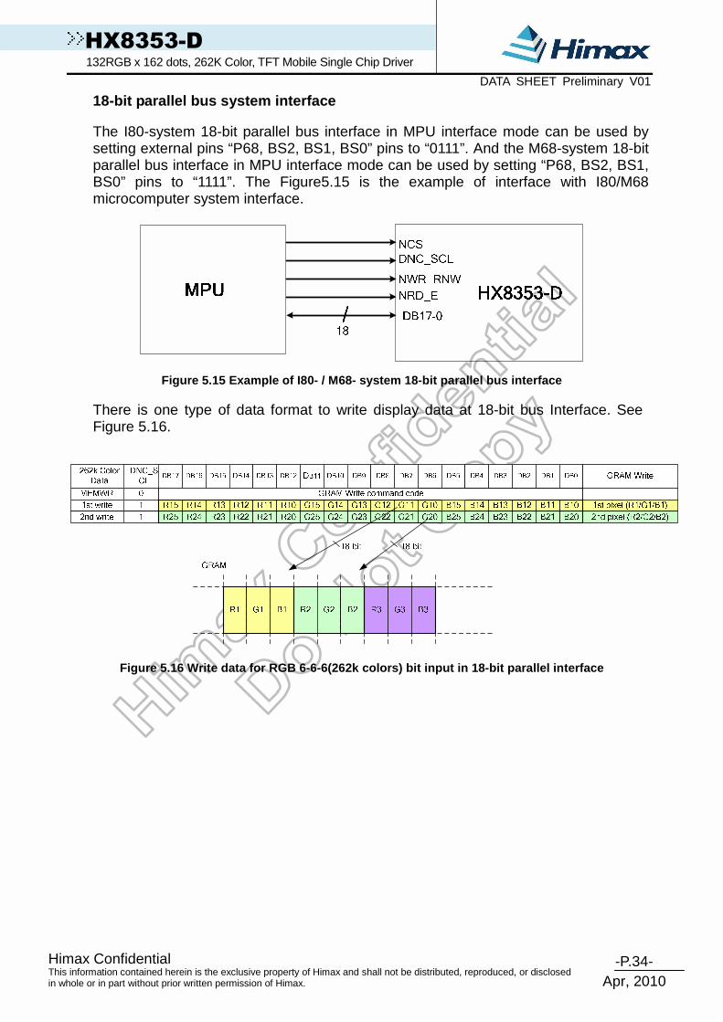
-P.34- Himax Confidential
Apr, 2010
This information contained herein is the exclusive property of Himax and shall not be distributed, reproduced, or disclosed in whole or in part without prior written permission of Himax.
HX8353-D 132RGB x 162 dots, 262K Color, TFT Mobile Single Chip Driver DATA SHEET Preliminary V01
18-bit parallel bus system interface The I80-system 18-bit parallel bus interface in MPU interface mode can be used by setting external pins “P68, BS2, BS1, BS0” pins to “0111”. And the M68-system 18-bit parallel bus interface in MPU interface mode can be used by setting “P68, BS2, BS1, BS0” pins to “1111”. The Figure5.15 is the example of interface with I80/M68 microcomputer system interface.
Figure 5.15 Example of I80- / M68- system 18-bit pa rallel bus interface
There is one type of data format to write display data at 18-bit bus Interface. See Figure 5.16.
Figure 5.16 Write data for RGB 6-6-6(262k colors) b it input in 18-bit parallel interface

-P.35- Himax Confidential
Apr, 2010
This information contained herein is the exclusive property of Himax and shall not be distributed, reproduced, or disclosed in whole or in part without prior written permission of Himax.
HX8353-D 132RGB x 162 dots, 262K Color, TFT Mobile Single Chip Driver DATA SHEET Preliminary V01
9-bit bus interface The I80-system 9-bit parallel bus interface in MPU interface mode can be used by setting external pins “P68, BS2, BS1, BS0” pins to “0110”. And the M68-system 9-bit parallel bus interface in MPU interface mode can be used by setting “P68, BS2, BS1, BS0” pins to “1110”. The Figure5.17 is the example of interface with I80/M68 microcomputer system interface.
/9
/9
DB17-9
NRD_E
NWR_RNW
NCS
DB8-0
DNC_SCL
Figure 5.17 Example of 80- / 68- system 9-bit bus i nterface
There is one type of data format to write display data at 9-bit bus Interface. See Figure 5.18.
Figure 5.18 Write data for RGB 6-6-6-bit (262k colo rs) input in 9-bit parallel interface

-P.36- Himax Confidential
Apr, 2010
This information contained herein is the exclusive property of Himax and shall not be distributed, reproduced, or disclosed in whole or in part without prior written permission of Himax.
HX8353-D 132RGB x 162 dots, 262K Color, TFT Mobile Single Chip Driver DATA SHEET Preliminary V01
MCU Data Color Coding for RAM data Read
- Parallel 8-Bit Bus Interface (BS2,BS1,BS0=”100”) D17 D16 D15 D14 D13 D12 D11 D10 D9 D8 D7 D6 D5 D4 D3 D2 D1 D0 Command Register
Command x x x x x x x x x x 0 0 1 0 1 1 1 0 2EH D17 D16 D15 D14 D13 D12 D11 D10 D9 D8 D7 D6 D5 D4 D3 D2 D1 D0 Color x x x x x x x x x x x x x x x x x x Dummy Read x x x x x x x x x x R5 R4 R3 R2 R1 R0 x x x x x x x x x x x x G5 G4 G3 G2 G1 G0 x x
Read Data Format
x x x x x x x x x x B5 B4 B3 B2 B1 B0 x x
262K-Color (1-pixel/ 3bytes)
Table 5.9 8-bit parallel interface GRAM read table
- Parallel 16-Bit Bus Interface (BS2,BS1,BS0=”101”)
D17 D16 D15 D14 D13 D12 D11 D10 D9 D8 D7 D6 D5 D4 D3 D2 D1 D0 Command Register Command x x x x x x x x x x 0 0 1 0 1 1 1 0 2EH
D17 D16 D15 D14 D13 D12 D11 D10 D9 D8 D7 D6 D5 D4 D3 D2 D1 D0 Color x x x x x x x x x x x x x x x x x x Dummy Read x x R5 R4 R3 R2 R1 R0 x x G5 G4 G3 G2 G1 G0 x x x x B5 B4 B3 B2 B1 B0 x x R5 R4 R3 R2 R1 R0 x x
Read Data Format
x x G5 G4 G3 G2 G1 G0 x x B5 B4 B3 B2 B1 B0 x x
262K-Color (2-pixel/ 3bytes)
Table 5.10 16-bit parallel interface GRAM read tabl e
- Parallel 9-Bit Bus Interface (BS2,BS1,BS0=”110”) D17 D16 D15 D14 D13 D12 D11 D10 D9 D8 D7 D6 D5 D4 D3 D2 D1 D0 Register Register
Command x x x x x x x x x x 0 0 1 0 1 1 1 0 2EH D17 D16 D15 D14 D13 D12 D11 D10 D9 D8 D7 D6 D5 D4 D3 D2 D1 D0 Color x x x x x x x x x x x x x x x x x x Dummy Read x x x x x x x x x R5 R4 R3 R2 R1 R0 G5 G4 G3
Read Data Format
x x x x x x x x x G2 G1 G0 B5 B4 B3 B2 B1 B0 262K-Color
(1-pixel/ 2bytes)
Table 5.11 9-bit parallel interface GRAM read table
- Parallel 18-Bit Bus Interface (BS2,BS1,BS0=”111”) D17 D16 D15 D14 D13 D12 D11 D10 D9 D8 D7 D6 D5 D4 D3 D2 D1 D0 Register Register
Command x x x x x x x x x x 0 0 1 0 1 1 1 0 2EH D17 D16 D15 D14 D13 D12 D11 D10 D9 D8 D7 D6 D5 D4 D3 D2 D1 D0 Color x x x x x x x x x x x x x x x x x x Dummy Read
Read Data Format
R5 R4 R3 R2 R1 R0 G5 G4 G3 G2 G1 G0 B5 B4 B3 B2 B1 B0 262K-Color
Table 5.12 18-bit parallel interface GRAM read tabl e

-P.37- Himax Confidential
Apr, 2010
This information contained herein is the exclusive property of Himax and shall not be distributed, reproduced, or disclosed in whole or in part without prior written permission of Himax.
HX8353-D 132RGB x 162 dots, 262K Color, TFT Mobile Single Chip Driver DATA SHEET Preliminary V01
5.1.3 Serial Interface
The HX8353-D supports serial data transfer interface. The interface selection by setting BS2=0 for serial interface mode. The 3-wires serial bus and 4-wires serial bus is select by SPI_SEL pin. When SPI_SEL pin is low (VSSD), it is selected by 3-wires serial bus and use: chip select line (NCS), serial input/output data (SDA), and the serial transfer clock line (DNC_SCL). When SPI_SEL pin is high (IOVCC), it is selected by 4-wires serial bus and use: chip select line (NCS), serial input/output data (SDA), and the serial transfer clock line (DNC_SCL) and the command or data transfer signal (NWR_RNW). Serial data write mode The 3-wires serial data packet contains a control bit DNC and a transmission byte, and in 4-wires serial case data packet contains just transmission byte and control bit DNC is transferred by NWR_RNW pin. If NWR_RNW is low, the transmission byte is command byte. If NWR_RNW is high, the transmission byte is stored to command register or GRAM. The MSB is transmitted first. The serial interface is initialized when NCS is high. In this state, DNC_SCL clock pulse or SDA data have no effect. A falling edge on NCS enables the serial interface and indicates the start of data transmission.
Figure 5.19 Serial interface protocol 3-/4- wire, w rite mode

-P.38- Himax Confidential
Apr, 2010
This information contained herein is the exclusive property of Himax and shall not be distributed, reproduced, or disclosed in whole or in part without prior written permission of Himax.
HX8353-D 132RGB x 162 dots, 262K Color, TFT Mobile Single Chip Driver DATA SHEET Preliminary V01
Serial data read mode
The microcontroller first has to send a command and then the following byte is transmitted in the opposite direction. The read mode has three type command data transmitted (8- / 24- / 32-bit) is according command code. 3-Wire Serial Interface Protocol
Figure 5.20 3-wire serial interface protocol, read mode

-P.39- Himax Confidential
Apr, 2010
This information contained herein is the exclusive property of Himax and shall not be distributed, reproduced, or disclosed in whole or in part without prior written permission of Himax.
HX8353-D 132RGB x 162 dots, 262K Color, TFT Mobile Single Chip Driver DATA SHEET Preliminary V01
4-Wire Serial Interface Protocol
Figure 5.21 4-wire serial interface protocol, read mode

-P.40- Himax Confidential
Apr, 2010
This information contained herein is the exclusive property of Himax and shall not be distributed, reproduced, or disclosed in whole or in part without prior written permission of Himax.
HX8353-D 132RGB x 162 dots, 262K Color, TFT Mobile Single Chip Driver DATA SHEET Preliminary V01
The data format that write display data to SRAM at Serial data bus Interface is shown as Figure5. 22 ~ Figure5. 27.
Figure 5.22 3-wire serial write data for RGB (6-6-6 ) bit input
Look-Up Table for 4K Color data mapping (12-bit to 18-bit)
12-bit
R1 G1 B1 R2 G2 B2 R3 G3 B3
18-bit 18-bitGRAM
R12 R10R11 B10B111 R22 R20R211
DNC_SCL
SDA B12B13 R23R13 G12 G10G11G13
Figure 5.23 3-wire serial write data for RGB 4-4-4- bit input
Look-Up Table for 65K Color data mapping (16-bit to 18-bit)
16-bit
R1 G1 B1 R2 G2 B2 R3 G3 B3
18-bit 18-bitGRAM
R13 R11R12 B141 1
DNC_SCL
SDA R14 G15 G13G14R10 G12 G11 G10 B13 B12 B11 B10
Figure 5.24 3-wire serial write data for RGB 5-6-5- bit input

-P.41- Himax Confidential
Apr, 2010
This information contained herein is the exclusive property of Himax and shall not be distributed, reproduced, or disclosed in whole or in part without prior written permission of Himax.
HX8353-D 132RGB x 162 dots, 262K Color, TFT Mobile Single Chip Driver DATA SHEET Preliminary V01
Figure 5.25 4-wire serial write data for RGB (6-6-6 ) bit input
Look-Up Table for 4K Color data mapping (12-bit to 18-bit)
12-bit
R1 G1 B1 R2 G2 B2 R3 G3 B3
18-bit 18-bitGRAM
R12 R10R11 B10B11 R22 R20R21
DNC_SCL
SDA B12B13 R23R13 G12 G10G11G13
1NWR_RNW 1
Figure 5.26 4-wire serial write data for RGB 4-4-4- bit input
Look-Up Table for 65K Color data mapping (16-bit to 18-bit)
16-bit
R1 G1 B1 R2 G2 B2 R3 G3 B3
18-bit 18-bitGRAM
R13 R11R12 B14
DNC_SCL
SDA R14 G15 G13G14R10 G12 G11 G10 B13 B12 B11 B10
1NWR_RNW 1
Figure 5.27 4-wire serial write data for RGB 5-6-5- bit input

-P.42- Himax Confidential
Apr, 2010
This information contained herein is the exclusive property of Himax and shall not be distributed, reproduced, or disclosed in whole or in part without prior written permission of Himax.
HX8353-D 132RGB x 162 dots, 262K Color, TFT Mobile Single Chip Driver DATA SHEET Preliminary V01
5.1.4 Display module data transfer recovery
If there is a break on data transmission when transmitting a command before a whole byte has been completed, then the display module will reset the interface so that it will be ready to receive the same byte re-transmitted when the chip select line (NCS) is next activated. See the following figure.
Figure 5.28 Display module data transfer recovery
If 1 or more parameter command is being sent and a break occurs while sending any parameter before the last one and if the host then sends a new command rather than re-transmitting the parameter that was interrupted, then the parameters that were successfully sent are stored and the parameter where the break occurred is rejected. The interface is ready to receive next byte as shown:
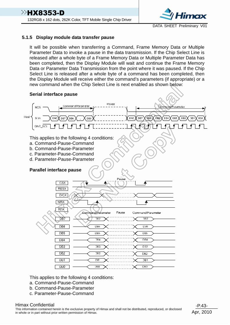
-P.43- Himax Confidential
Apr, 2010
This information contained herein is the exclusive property of Himax and shall not be distributed, reproduced, or disclosed in whole or in part without prior written permission of Himax.
HX8353-D 132RGB x 162 dots, 262K Color, TFT Mobile Single Chip Driver DATA SHEET Preliminary V01
5.1.5 Display module data transfer pause
It will be possible when transferring a Command, Frame Memory Data or Multiple Parameter Data to invoke a pause in the data transmission. If the Chip Select Line is released after a whole byte of a Frame Memory Data or Multiple Parameter Data has been completed, then the Display Module will wait and continue the Frame Memory Data or Parameter Data Transmission from the point where it was paused. If the Chip Select Line is released after a whole byte of a command has been completed, then the Display Module will receive either the command’s parameters (if appropriate) or a new command when the Chip Select Line is next enabled as shown below:
Serial interface pause
This applies to the following 4 conditions: a. Command-Pause-Command b. Command-Pause-Parameter c. Parameter-Pause-Command d. Parameter-Pause-Parameter Parallel interface pause
This applies to the following 4 conditions: a. Command-Pause-Command b. Command-Pause-Parameter c. Parameter-Pause-Command

-P.44- Himax Confidential
Apr, 2010
This information contained herein is the exclusive property of Himax and shall not be distributed, reproduced, or disclosed in whole or in part without prior written permission of Himax.
HX8353-D 132RGB x 162 dots, 262K Color, TFT Mobile Single Chip Driver DATA SHEET Preliminary V01
d. Parameter-Pause-Parameter 5.1.6 Display module data transfer modes
The Module has three colour modes for transferring data to the display RAM. These are 12-bit colour per pixel, 16-bit colour per pixel and 18-bit colour per pixel. The data format is described for each interface. Data can be downloaded to the Frame Memory by 2 methods. Method 1: The Image data is sent to the Frame Memory in successive Frame writes, each time the Frame Memory is filled, the Frame Memory pointer is reset to the start point and the next Frame is written.
Method 2: Image Data is sent and at the end of each Frame Memory download, a command is sent to stop Frame Memory Write. Then Start Memory Write command is sent, and a new Frame is downloaded.
Start Frame
Memory
Write
Image Data
Frame 1
Any
Command
Start Frame
Memory
Write
Image Data
Frame 2
Any
Command
Any
Command
StopStart
Note: (1) These apply to all Data Transfer Colour modes on both Serial and Parallel interfaces. (2) The Frame Memory can contain both odd and even number of pixels for both Methods. Only complete pixel
data will be stored in the Frame Memory.

-P.45- Himax Confidential
Apr, 2010
This information contained herein is the exclusive property of Himax and shall not be distributed, reproduced, or disclosed in whole or in part without prior written permission of Himax.
HX8353-D 132RGB x 162 dots, 262K Color, TFT Mobile Single Chip Driver DATA SHEET Preliminary V01
5.2 Color depth conversion
R input (4bit)
12 bit/pixel -mode 4,096 colors
R input (5 bit) 16 bit/pixel -mode
65,536 colors
R output (6bit) 18 bit/pixel -mode
262,144 colors RGBSET Parameter
0000 00000 R005 R004 R003 R002 R001 R000 1 0001 00001 R015 R014 R013 R012 R011 R010 2 0010 00010 R025 R024 R023 R022 R021 R020 3 0011 00011 R035 R034 R033 R032 R031 R030 4 0100 00100 R045 R044 R043 R042 R041 R040 5 0101 00101 R055 R054 R053 R052 R051 R050 6 0110 00110 R065 R064 R063 R062 R061 R060 7 0111 00111 R075 R074 R073 R072 R071 R070 8 1000 01000 R085 R084 R083 R082 R081 R080 9 1001 01001 R095 R094 R093 R092 R091 R090 10 1010 01010 R105 R104 R103 R102 R101 R100 11 1011 01011 R115 R114 R113 R112 R111 R110 12 1100 01100 R125 R124 R123 R122 R121 R120 13 1101 01101 R135 R134 R133 R132 R131 R130 14 1110 01110 R145 R144 R143 R142 R141 R140 15 1111 01111 R155 R154 R153 R152 R151 R150 16
No Input 10000 R165 R164 R163 R162 R161 R160 17 No Input 10001 R175 R174 R173 R172 R171 R170 18 No Input 10010 R185 R184 R183 R182 R181 R180 19 No Input 10011 R195 R194 R193 R192 R191 R190 20 No Input 10100 R205 R204 R203 R202 R201 R200 21 No Input 10101 R215 R214 R213 R212 R211 R210 22 No Input 10110 R225 R224 R223 R222 R221 R220 23 No Input 10111 R235 R234 R233 R232 R231 R230 24 No Input 11000 R245 R244 R243 R242 R241 R240 25 No Input 11001 R255 R254 R253 R252 R251 R250 26 No Input 11010 R265 R264 R263 R262 R261 R260 27 No Input 11011 R275 R274 R273 R272 R271 R270 28 No Input 11100 R285 R284 R283 R282 R281 R280 29 No Input 11101 R295 R294 R293 R292 R291 R290 30 No Input 11110 R305 R304 R303 R302 R301 R300 31 No Input 11111 R315 R314 R313 R312 R311 R310 32

-P.46- Himax Confidential
Apr, 2010
This information contained herein is the exclusive property of Himax and shall not be distributed, reproduced, or disclosed in whole or in part without prior written permission of Himax.
HX8353-D 132RGB x 162 dots, 262K Color, TFT Mobile Single Chip Driver DATA SHEET Preliminary V01
G input (4bit)
12 bit/pixel -mode 4,096 colors
G input (6 bit) 16 bit/pixel -mode
65,536 colors
G output (6bit) 18 bit/pixel -mode
262,144 colors RGBSET Parameter
0000 000000 G005 G004 G003 G002 G001 G000 33 0001 000001 G015 G014 G013 G012 G011 G010 34 0010 000010 G025 G024 G023 G022 G021 G020 35 0011 000011 G035 G034 G033 G032 G031 G030 36 0100 000100 G045 G044 G043 G042 G041 G040 37 0101 000101 G055 G054 G053 G052 G051 G050 38 0110 000110 G065 G064 G063 G062 G061 G060 39 0111 000111 G075 G074 G073 G072 G071 G070 40 1000 001000 G085 G084 G083 G082 G081 G080 41 1001 001001 G095 G094 G093 G092 G091 G090 42 1010 001010 G105 G104 G103 G102 G101 G100 43 1011 001011 G115 G114 G113 G112 G111 G110 44 1100 001100 G125 G124 G123 G122 G121 G120 45 1101 001101 G135 G134 G133 G132 G131 G130 46 1110 001110 G145 G144 G143 G142 G141 G140 47 1111 001111 G155 G154 G153 G152 G151 G150 48
No Input 010000 G165 G164 G163 G162 G161 G160 49 No Input 010001 G175 G174 G173 G172 G171 G170 50 No Input 010010 G185 G184 G183 G182 G181 G180 51 No Input 010011 G195 G194 G193 G192 G191 G190 52 No Input 010100 G205 G204 G203 G202 G201 G200 53 No Input 010101 G215 G214 G213 G212 G211 G210 54 No Input 010110 G225 G224 G223 G222 G221 G220 55 No Input 010111 G235 G234 G233 G232 G231 G230 56 No Input 011000 G245 G244 G243 G242 G241 G240 57 No Input 011001 G255 G254 G253 G252 G251 G250 58 No Input 011010 G265 G264 G263 G262 G261 G260 59 No Input 011011 G275 G274 G273 G272 G271 G270 60 No Input 011100 G285 G284 G283 G282 G281 G280 61 No Input 011101 G295 G294 G293 G292 G291 G290 62 No Input 011110 G305 G304 G303 G302 G301 G300 63 No Input 011111 G315 G314 G313 G312 G311 G310 64

-P.47- Himax Confidential
Apr, 2010
This information contained herein is the exclusive property of Himax and shall not be distributed, reproduced, or disclosed in whole or in part without prior written permission of Himax.
HX8353-D 132RGB x 162 dots, 262K Color, TFT Mobile Single Chip Driver DATA SHEET Preliminary V01
G input (4bit)
12 bit/pixel -mode 4,096 colors
G input (6 bit) 16 bit/pixel -mode
65,536 colors
G output (6bit) 18 bit/pixel -mode
262,144 colors RGBSET Parameter
No Input 100000 G325 G324 G323 G322 G321 G320 65 No Input 100001 G335 G334 G333 G332 G331 G330 66 No Input 100010 G345 G344 G343 G342 G341 G340 67 No Input 100011 G355 G354 G353 G352 G351 G350 68 No Input 100100 G365 G364 G363 G362 G361 G360 69 No Input 100101 G375 G374 G373 G372 G371 G370 70 No Input 100110 G385 G384 G383 G382 G381 G380 71 No Input 100111 G395 G394 G393 G392 G391 G390 72 No Input 101000 G405 G404 G403 G402 G401 G400 73 No Input 101001 G415 G414 G413 G412 G411 G410 74 No Input 101010 G425 G424 G423 G422 G421 G420 75 No Input 101011 G435 G434 G433 G432 G431 G430 76 No Input 101100 G445 G444 G443 G442 G441 G440 77 No Input 101101 G455 G454 G453 G452 G451 G450 78 No Input 101110 G465 G464 G463 G462 G461 G460 79 No Input 101111 G475 G474 G473 G472 G471 G470 80 No Input 110000 G485 G484 G483 G482 G481 G480 81 No Input 110001 G495 G494 G493 G492 G491 G490 82 No Input 110010 G505 G504 G503 G502 G501 G500 83 No Input 110011 G515 G514 G513 G512 G511 G510 84 No Input 110100 G525 G524 G523 G522 G521 G520 85 No Input 110101 G535 G534 G533 G532 G531 G530 86 No Input 110110 G545 G544 G543 G542 G541 G540 87 No Input 110111 G555 G554 G553 G552 G551 G550 88 No Input 111000 G565 G564 G563 G562 G561 G560 89 No Input 111001 G575 G574 G573 G572 G571 G570 90 No Input 111010 G585 G584 G583 G582 G581 G580 91 No Input 111011 G595 G594 G593 G592 G591 G590 92 No Input 111100 G605 G604 G603 G602 G601 G600 93 No Input 111101 G615 G614 G613 G612 G611 G610 94 No Input 111110 G625 G624 G623 G622 G621 G620 95 No Input 111111 G635 G634 G533 G632 G631 G630 96

-P.48- Himax Confidential
Apr, 2010
This information contained herein is the exclusive property of Himax and shall not be distributed, reproduced, or disclosed in whole or in part without prior written permission of Himax.
HX8353-D 132RGB x 162 dots, 262K Color, TFT Mobile Single Chip Driver DATA SHEET Preliminary V01
B input (4bit)
12 bit/pixel -mode 4,096 colors
B input (5 bit) 16 bit/pixel -mode
65,536 colors
B output (6bit) 18 bit/pixel -mode
262,144 colors RGBSET Parameter
0000 00000 B005 B004 B003 B002 B001 B000 97 0001 00001 B015 B014 B013 B012 B011 B010 98 0010 00010 B025 B024 B023 B022 B021 B020 99 0011 00011 B035 B034 B033 B032 B031 B030 100 0100 00100 B045 B044 B043 B042 B041 B040 101 0101 00101 B055 B054 B053 B052 B051 B050 102 0110 00110 B065 B064 B063 B062 B061 B060 103 0111 00111 B075 B074 B073 B072 B071 B070 104 1000 01000 B085 B084 B083 B082 B081 B080 105 1001 01001 B095 B094 B093 B092 B091 B090 106 1010 01010 B105 B104 B103 B102 B101 B100 107 1011 01011 B115 B114 B113 B112 B111 B110 108 1100 01100 B125 B124 B123 B122 B121 B120 109 1101 01101 B135 B134 B133 B132 B131 B130 110 1110 01110 B145 B144 B143 B142 B141 B140 111 1111 01111 B155 B154 B153 B152 B151 B150 112
No Input 10000 B165 B164 B163 B162 B161 B160 113 No Input 10001 B175 B174 B173 B172 B171 B170 114 No Input 10010 B185 B184 B183 B182 B181 B180 115 No Input 10011 B195 B194 B193 B192 B191 B190 116 No Input 10100 B205 B204 B203 B202 B201 B200 117 No Input 10101 B215 B214 B213 B212 B211 B210 118 No Input 10110 B225 B224 B223 B222 B221 B220 119 No Input 10111 B235 B234 B233 B232 B231 B230 120 No Input 11000 B245 B244 B243 B242 B241 B240 121 No Input 11001 B255 B254 B253 B252 B251 B250 122 No Input 11010 B265 B264 B263 B262 B261 B260 123 No Input 11011 B275 B274 B273 B272 B271 B270 124 No Input 11100 B285 B284 B283 B282 B281 B280 125 No Input 11101 B295 B294 B293 B292 B291 B290 126 No Input 11110 B305 B304 B303 B302 B301 B300 127 No Input 11111 B315 B314 B313 B312 B311 B310 128

-P.49- Himax Confidential
Apr, 2010
This information contained herein is the exclusive property of Himax and shall not be distributed, reproduced, or disclosed in whole or in part without prior written permission of Himax.
HX8353-D 132RGB x 162 dots, 262K Color, TFT Mobile Single Chip Driver DATA SHEET Preliminary V01
6. Display Data GRAM
The display data RAM stores display dots and consists of 384,912 bits (132x18x162 bits). There is no restriction on access to the RAM even when the display data on the same address is loaded to DAC. There will be no abnormal visible effect on the display when there is a simultaneous Panel Read and Interface Read or Write to the same location of the Frame Memory.
6.1 Display data GRAM mapping
Every pixel (18-bit) data in GRAM is located by a (Page, Column) address (Y, X). By specifying the arbitrary window address CASET’s SC, EC and PASET’s SP, EP , it is possible to access the GRAM by setting RAMWR or RAMRD commands from start positions of the window address.
0000H 0001H 0002H 0003H --------- 0080H 0081H 0082H 0083H 0100H 0101H 0102H 0103H --------- 0180H 0181H 0182H 0183H 0200H 0201H 0202H 0203H --------- 0280H 0281H 0282H 0283H 0300H 0301H 0302H 0303H --------- 0380H 0381H 0382H 0383H 0400H 0401H 0402H 0403H --------- 0480H 0481H 0482H 0483H 0500H 0501H 0502H 0503H --------- 0580H 0581H 0582H 0583H
-------
-------
-------
-------
---------
-------
-------
-------
-------
9C00H 9C01H 9C02H 9C03H --------- 9C80H 9C81H 9C82H 9C83H 9D00H 9D01H 9D02H 9D03H --------- 9D80H 9D81H 9D82H 9D83H 9E00H 9E01H 9E02H 9E03H --------- 9E80H 9E81H 9E82H 9E83H 9F00H 9F01H 9F02H 9F03H --------- 9F80H 9F81H 9F82H 9F83H A000H A001H A002H A003H --------- A080H A081H A082H A083H A100H A101H A102H A103H --------- A180H A181H A182H A183H
Table 6.1 GRAM address for display panel position 6.2 Address counter (AC) of GRAM
The HX8353-D contains an address counter (AC) which assigns address for writing/reading pixel data to/from GRAM. The address pointers set the position of GRAM. Every time when a pixel data is written into the GRAM, the X address or Y address of AC will be automatically increased by 1 (or decreased by 1), which is decided by the register (MADTCL’s MV(B5), MX(B6) and MY(B7) bits) setting. To simplify the address control of GRAM access, the window address function allows for writing data only to a window area of GRAM specified by registers. After data being written to the GRAM, the AC will be increased or decreased within setting window address-range which is specified by the CASET (start: SC, end: EC) and the PASET (start: SP, end: EP). Therefore, the data can be written consecutively without thinking a data wrap by those bit function.
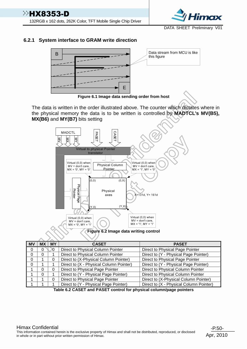
-P.50- Himax Confidential
Apr, 2010
This information contained herein is the exclusive property of Himax and shall not be distributed, reproduced, or disclosed in whole or in part without prior written permission of Himax.
HX8353-D 132RGB x 162 dots, 262K Color, TFT Mobile Single Chip Driver DATA SHEET Preliminary V01
6.2.1 System interface to GRAM write direction
B
E
Data stream from MCU is likethis figure
Figure 6.1 Image data sending order from host
The data is written in the order illustrated above. The counter which dictates where in the physical memory the data is to be written is controlled by MADTCL’s MV(B5), MX(B6) and MY(B7) bits setting
MADCTL
Physical Column
PointerPhysica
l Page
Pointe
r
CASET
PASET
MV
MX
MY
Physical
axes
Virtual to physical Pointer
transtator
Virtual (0,0) when
MV = don't care, MX = '0', MY = '0'
(0,0) (0,X)
Virtual (0,0) when
MV = don't care, MX = '1', MY = '0'
Virtual (0,0) when MV = don't care,
MX = '0', MY = '1'
(Y,0) (Y,X)
Virtual (0,0) when MV = don't care,
MX = '1', MY = '1'
X=131d, Y= 161d
Figure 6.2 Image data writing control
MV MX MY CASET PASET 0 0 0 Direct to Physical Column Pointer Direct to Physical Page Pointer 0 0 1 Direct to Physical Column Pointer Direct to (Y - Physical Page Pointer) 0 1 0 Direct to (X-Physical Column Pointer) Direct to Physical Page Pointer 0 1 1 Direct to (X - Physical Column Pointer) Direct to (Y - Physical Page Pointer) 1 0 0 Direct to Physical Page Pointer Direct to Physical Column Pointer 1 0 1 Direct to (Y - Physical Page Pointer) Direct to Physical Column Pointer 1 1 0 Direct to Physical Page Pointer Direct to (X-Physical Column Pointer) 1 1 1 Direct to (Y - Physical Page Pointer) Direct to (X - Physical Column Pointer)
Table 6.2 CASET and PASET control for physical colu mn/page pointers

-P.51- Himax Confidential
Apr, 2010
This information contained herein is the exclusive property of Himax and shall not be distributed, reproduced, or disclosed in whole or in part without prior written permission of Himax.
HX8353-D 132RGB x 162 dots, 262K Color, TFT Mobile Single Chip Driver DATA SHEET Preliminary V01
For each image orientation, the controls for the column and page counters apply as below:
Condition Column Counter Page Counter
When RAMWR/RAMRD command is accepted. Return to “Start Column”
Return to “Start Page”
Complete Pixel Pair Write/Read action Increment by 1 No change
The Column counter value is larger than “End column.” Return to
“Start Column” Increment by 1
The Page counter value is larger than “End page”. Return to
“Start Column” Return to
“Start Page” Note: Data is always written to the Frame Memory in the same order, regardless of the Memory Write
Direction set by MADCTL bits B7, B6 and B5. Table 6.3 Rules for updating GRAM order

-P.52- Himax Confidential
Apr, 2010
This information contained herein is the exclusive property of Himax and shall not be distributed, reproduced, or disclosed in whole or in part without prior written permission of Himax.
HX8353-D 132RGB x 162 dots, 262K Color, TFT Mobile Single Chip Driver DATA SHEET Preliminary V01
The following figure depicts the GRAM address update method with MV, MX and MY bit setting.
MADCTR parameter
Display Data
Direction MV MX MY
Image in the Host Image in the Driver (GRAM)
Normal 0 0 0
B
E
Y-Invert 0 0 1
B
E
X-Invert 0 1 0
B
E
X-Invert Y-Invert 0 1 1
B
E
X-Y Exchange
1 0 0
B
E
X,Y address (0,0)X: CASETY: RASET
B
E
H/W Position (0,0)
X-Y Exchange X-invert
1 0 1
B
E
X,Y address (0,0)X: CASETY: RASET
H/W Position (0,0)
B
E
X-Y Exchange Y-invert
1 1 0
B
E
X-Y Exchange X-invert Y-invert
1 1 1
B
E
X,Y address (0,0)X: CASETY: RASET
H/W Position (0,0)
B
E
Table 6.4 Address direction settings
H/W Position (0,0)
X,Y address (0,0)X: CASET Y: RASET
B
E
H/W Position (0,0)
X,Y address (0,0) X: CASET Y: RASET B
E
B
E
H/W Position (0,0) X,Y address (0,0) X: CASET Y: RASET
H/W Position (0,0)
B
E
X,Y address (0,0) X: CASET Y: RASET
X ,Y address ( 0, 0)X : CASET Y : RASET
H /W Position (0, 0) B
E

-P.53- Himax Confidential
Apr, 2010
This information contained herein is the exclusive property of Himax and shall not be distributed, reproduced, or disclosed in whole or in part without prior written permission of Himax.
HX8353-D 132RGB x 162 dots, 262K Color, TFT Mobile Single Chip Driver DATA SHEET Preliminary V01
Example for rotation with MY, MX and MV This example is using following values: start page=0, end page=40, start column=0 and end column=20=> commands: page address set (0, 40) and column address set (0, 20). The sent figure is as follows and its sending order is as follows.
Written image and direction from the host to frame memory
Start
End
Writieg direction Image from the host
Start page=0
End page=40
Start column =0 End column=20
Image position on the frame memory with MYImage position on the frame memory with MYImage position on the frame memory with MYImage position on the frame memory with MY
Memory
Location
(0,0)FRAM
E MEMOR
Y
==== 0000 ////1111 , , , , MXMXMXMX ==== 0000 ////1111 , , , , MVMVMVMV ==== 0000 ////1 1 1 1
MY=0
MX=0
MV=0
Memory
Location
(0,0)FRAM
E MEMOR
Y
MY=0
MX=1
MV=0
Memory
Location
(0,0)FRAM
E MEMOR
Y
MY=1
MX=0
MV=0
Memory
Location
(0,0)FRAM
E MEMOR
Y
MY=1
MX=1
MV=0
Figure 6.3 Example for rotation with MY, MX and MV – 1

-P.54- Himax Confidential
Apr, 2010
This information contained herein is the exclusive property of Himax and shall not be distributed, reproduced, or disclosed in whole or in part without prior written permission of Himax.
HX8353-D 132RGB x 162 dots, 262K Color, TFT Mobile Single Chip Driver DATA SHEET Preliminary V01
Written image and direction from the host to frame memory
Start
End
Writieg direction Image from the host
Start page=0
End page=40
Start column =0 End column=20
Image position on the frame memory with MYImage position on the frame memory with MYImage position on the frame memory with MYImage position on the frame memory with MY
Memory
Location
(0,0)FRAM
E MEMOR
Y
==== 0000 ////1111 , , , , MXMXMXMX ==== 0000 ////1111 , , , , MVMVMVMV ==== 0000 ////1 1 1 1
MY=0
MX=0
MV=1
Memory
Location
(0,0)FRAM
E MEMOR
Y
MY=0
MX=1
MV=1
Memory
Location
(0,0)FRAM
E MEMOR
Y
MY=1
MX=0
MV=1
Memory
Location
(0,0)FRAM
E MEMOR
Y
MY=1
MX=1
MV=1
Figure 6.4 Example for rotation with MY, MX and MV – 2
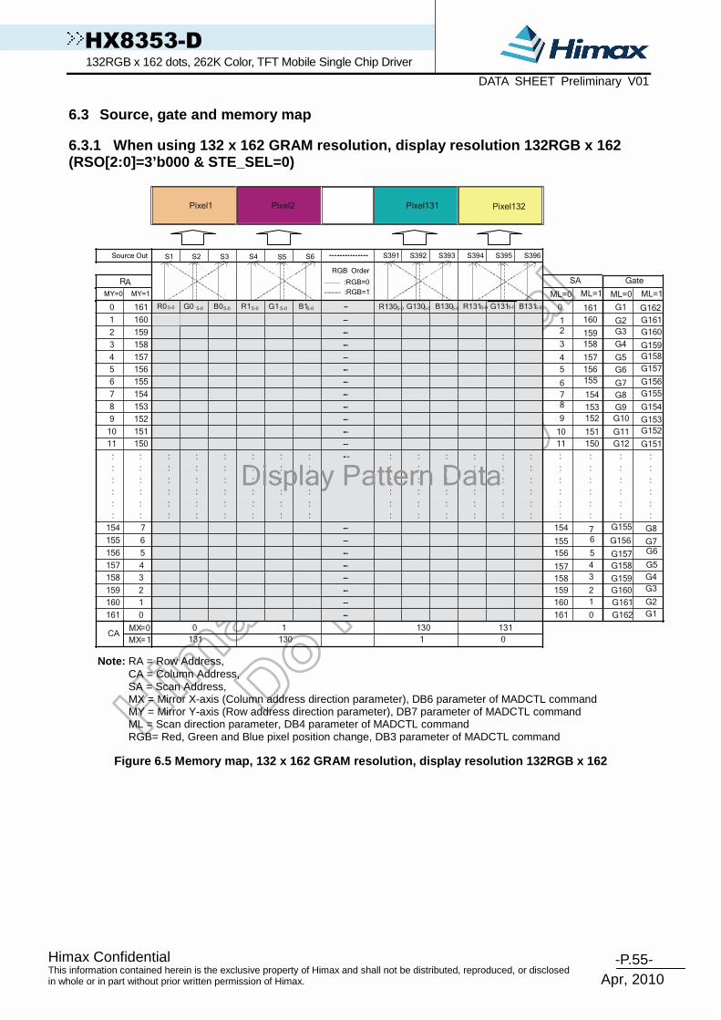
-P.55- Himax Confidential
Apr, 2010
This information contained herein is the exclusive property of Himax and shall not be distributed, reproduced, or disclosed in whole or in part without prior written permission of Himax.
HX8353-D 132RGB x 162 dots, 262K Color, TFT Mobile Single Chip Driver DATA SHEET Preliminary V01
6.3 Source, gate and memory map
6.3.1 When using 132 x 162 GRAM resolution, display resolution 132RGB x 162 (RSO[2:0]=3’b000 & STE_SEL=0)
Pixel1 Pixel2 Pixel131 Pixel132
RA SA
ML=0 ML=1
0 161 R0 G0 B0 R1 G1 B1 --- R130 G130 B130 R131 G131 B131 0 161
1 160 --- 1 160
2 159 --- 2 159
3 158 --- 3 158
4 157 --- 4 157
5 156 --- 5 156
6 155 --- 6 155
7 154 --- 7 154
8 153 --- 8 153
9 152 --- 9 152
10 151 --- 10 151
11 150 --- 11 150
:
:
:
:
:
:
:
:
:
:
:
:
:
:
:
:
:
:
:
:
:
:
:
:
:
:
:
:
:
:
:
:
:
:
:
:
:
:
:
:
:
:
:
:
:
:
:
:
--- :
:
:
:
:
:
:
:
:
:
:
:
:
:
:
:
:
:
:
:
:
:
:
:
:
:
:
:
:
:
:
:
:
:
:
:
:
:
:
:
:
:
:
:
:
:
:
:
154 7 --- 154 7
155 6 --- 155 6
156 5 --- 156 5
157 4 --- 157 4
158 3 --- 158 3
159 2 --- 159 2
160 1 --- 160 1
161 0 --- 161 0
MX=0 0 131CA
MX=1
Source Out S1 S2 S3 S4 S5 S6 S391 S392 S393 S394 S395 S396
MY=0 MY=1
1301
131 130 1 0
RGB Order
:RGB=0
:RGB=1
Display Pattern Data
5-0 5-0 5-0 5-0 5-0 5-0 5-0 5-0 5-0 5-0 5-0 5-0
Gate
ML=0 ML=1
G1
G161G2
G160G3
G159G4
G158G5
G157G6
G156G7
G155G8
G154G9
G153G10
G152G11
G151G12
:
:
:
:
:
:
:
:
:
:
:
:
G7
G155
G6
G156
G5
G157
G4G159G3G160
G2G161
G1G162
G158
G162
G8
Note: RA = Row Address, CA = Column Address, SA = Scan Address, MX = Mirror X-axis (Column address direction parameter), DB6 parameter of MADCTL command MY = Mirror Y-axis (Row address direction parameter), DB7 parameter of MADCTL command ML = Scan direction parameter, DB4 parameter of MADCTL command RGB= Red, Green and Blue pixel position change, DB3 parameter of MADCTL command
Figure 6.5 Memory map, 132 x 162 GRAM resolution, d isplay resolution 132RGB x 162

-P.56- Himax Confidential
Apr, 2010
This information contained herein is the exclusive property of Himax and shall not be distributed, reproduced, or disclosed in whole or in part without prior written permission of Himax.
HX8353-D 132RGB x 162 dots, 262K Color, TFT Mobile Single Chip Driver DATA SHEET Preliminary V01
6.3.2 When using 132 x 162 GRAM resolution, display resolution 128RGB x 160 (RSO[2:0]=3’b000 & STE_SEL=1)
Pixel1 Pixel2 Pixel127 Pixel128
RA SA
ML=0 ML=1
0 161 R0 G0 B0 R1 G1 B1 --- R126 G126 B126 R127 G127 B127 0 161
1 160 --- 1 160
2 159 --- 2 159
3 158 --- 3 158
4 157 --- 4 157
5 156 --- 5 156
6 155 --- 6 155
7 154 --- 7 154
8 153 --- 8 153
9 152 --- 9 152
10 151 --- 10 151
11 150 --- 11 150
:
:
:
:
:
:
:
:
:
:
:
:
:
:
:
:
:
:
:
:
:
:
:
:
:
:
:
:
:
:
:
:
:
:
:
:
:
:
:
:
:
:
:
:
:
:
:
:
--- :
:
:
:
:
:
:
:
:
:
:
:
:
:
:
:
:
:
:
:
:
:
:
:
:
:
:
:
:
:
:
:
:
:
:
:
:
:
:
:
:
:
:
:
:
:
:
:
154 7 --- 154 7
155 6 --- 155 6
156 5 --- 156 5
157 4 --- 157 4
158 3 --- 158 3
159 2 --- 159 2
160 1 --- 160 1
161 0 --- 161 0
MX=0 0 127CA
MX=1
Source Out S7 S8 S9 S10 S11 S12 S385 S386 S387 S388 S389 S390
MY=0 MY=1
1261
127 126 1 0
RGB Order
:RGB=0
:RGB=1
Display Pattern Data
5-0 5-0 5-0 5-0 5-0 5-0 5-0 5-0 5-0 5-0 5-0 5-0
Gate
ML=0 ML=1
G2
G160G3G159G4G158G5G157G6
G156G7
G155G8
G154G9
G153G10G152G11
G151G12
:
:
:
:
:
:
:
:
:
:
:
:
G8
G7
G155
G6
G156
G5G158
G4G159
G3G160
G2G161
G157
G161
--
--
--
--
Note: RA = Row Address, CA = Column Address, SA = Scan Address, MX = Mirror X-axis (Column address direction parameter), DB6 parameter of MADCTL command MY = Mirror Y-axis (Row address direction parameter), DB7 parameter of MADCTL command ML = Scan direction parameter, DB4 parameter of MADCTL command RGB= Red, Green and Blue pixel position change, DB3 parameter of MADCTL command
Figure 6.6 Memory map, 132 x 162 GRAM resolution, d isplay resolution 128RGB x 160
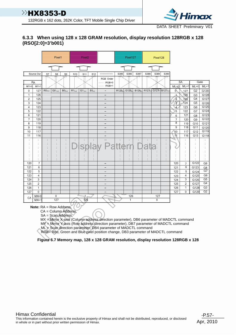
-P.57- Himax Confidential
Apr, 2010
This information contained herein is the exclusive property of Himax and shall not be distributed, reproduced, or disclosed in whole or in part without prior written permission of Himax.
HX8353-D 132RGB x 162 dots, 262K Color, TFT Mobile Single Chip Driver DATA SHEET Preliminary V01
6.3.3 When using 128 x 128 GRAM resolution, display resolution 128RGB x 128 (RSO[2:0]=3’b001)
Pixel1 Pixel2 Pixel127 Pixel128
RA SA
ML=0 ML=1
0 127 R0 G0 B0 R1 G1 B1 --- R126 G126 B126 R127 G127 B127 0 127
1 126 --- 1 126
2 125 --- 2 125
3 124 --- 3 124
4 123 --- 4 123
5 122 --- 5 122
6 121 --- 6 121
7 120 --- 7 120
8 119 --- 8 119
9 118 --- 9 118
10 117 --- 10 117
11 116 --- 11 116
:
:
:
:
:
:
:
:
:
:
:
:
:
:
:
:
:
:
:
:
:
:
:
:
:
:
:
:
:
:
:
:
:
:
:
:
:
:
:
:
:
:
:
:
:
:
:
:
--- :
:
:
:
:
:
:
:
:
:
:
:
:
:
:
:
:
:
:
:
:
:
:
:
:
:
:
:
:
:
:
:
:
:
:
:
:
:
:
:
:
:
:
:
:
:
:
:
120 7 --- 120 7
121 6 --- 121 6
122 5 --- 122 5
123 4 --- 123 4
124 3 --- 124 3
125 2 --- 125 2
126 1 --- 126 1
127 0 --- 127 0
MX=0 0 127CA
MX=1
Source Out S7 S8 S9 S10 S11 S12 S385 S386 S387 S388 S389 S390
MY=0 MY=1
1261
127 126 1 0
RGB Order
:RGB=0
:RGB=1
Display Pattern Data
5-0 5-0 5-0 5-0 5-0 5-0 5-0 5-0 5-0 5-0 5-0 5-0
Gate
ML=0 ML=1
G2
G128G3
G127G4
G126G5
G125G6
G124G7
G123G8
G122G9
G121G10
G120G11
G119G12
G118G13
:
:
:
:
:
:
:
:
:
:
:
:
G8
G122
G7
G123
G6
G124
G5G126G4G127
G3G128
G2G129
G125
G129
G9
Note: RA = Row Address,
CA = Column Address, SA = Scan Address, MX = Mirror X-axis (Column address direction parameter), DB6 parameter of MADCTL command MY = Mirror Y-axis (Row address direction parameter), DB7 parameter of MADCTL command ML = Scan direction parameter, DB4 parameter of MADCTL command RGB= Red, Green and Blue pixel position change, DB3 parameter of MADCTL command
Figure 6.7 Memory map, 128 x 128 GRAM resolution, d isplay resolution 128RGB x 128

-P.58- Himax Confidential
Apr, 2010
This information contained herein is the exclusive property of Himax and shall not be distributed, reproduced, or disclosed in whole or in part without prior written permission of Himax.
HX8353-D 132RGB x 162 dots, 262K Color, TFT Mobile Single Chip Driver DATA SHEET Preliminary V01
6.3.4 When using 120 x 160 GRAM resolution, display resolution 120RGB x 160 (RSO[2:0]=3’b010)
Pixel1 Pixel2 Pixel119 Pixel120
RA SA
ML=0 ML=1
0 159 R0 G0 B0 R1 G1 B1 --- R118 G118 B118 R119 G119 B119 0 159
1 158 --- 1 158
2 157 --- 2 157
3 156 --- 3 156
4 155 --- 4 155
5 154 --- 5 154
6 153 --- 6 153
7 152 --- 7 152
8 151 --- 8 151
9 150 --- 9 150
10 149 --- 10 149
11 148 --- 11 148
:
:
:
:
:
:
:
:
:
:
:
:
:
:
:
:
:
:
:
:
:
:
:
:
:
:
:
:
:
:
:
:
:
:
:
:
:
:
:
:
:
:
:
:
:
:
:
:
--- :
:
:
:
:
:
:
:
:
:
:
:
:
:
:
:
:
:
:
:
:
:
:
:
:
:
:
:
:
:
:
:
:
:
:
:
:
:
:
:
:
:
:
:
:
:
:
:
152 7 --- 152 7
153 6 --- 153 6
154 5 --- 154 5
155 4 --- 155 4
156 3 --- 156 3
157 2 --- 157 2
158 1 --- 158 1
159 0 --- 159 0
MX=0 0 119CA
MX=1
Source Out S7 S8 S9 S10 S11 S12 S361 S362 S363 S364 S365 S366
MY=0 MY=1
1181
119 118 1 0
RGB Order
:RGB=0
:RGB=1
Display Pattern Data
5-0 5-0 5-0 5-0 5-0 5-0 5-0 5-0 5-0 5-0 5-0 5-0
Gate
ML=0 ML=1
G2
G160G3
G159G4
G158G5
G157G6
G156G7
G155G8
G154G9
G153G10
G152G11
G151G12
G150G13
:
:
:
:
:
:
:
:
:
:
:
:
G8
G154
G7
G155
G6
G156
G5G158G4G159
G3G160
G2G161
G157
G161
G9
Note: RA = Row Address,
CA = Column Address, SA = Scan Address, MX = Mirror X-axis (Column address direction parameter), DB6 parameter of MADCTL command MY = Mirror Y-axis (Row address direction parameter), DB7 parameter of MADCTL command ML = Scan direction parameter, DB4 parameter of MADCTL command RGB= Red, Green and Blue pixel position change, DB3 parameter of MADCTL command
Figure 6.8 Memory map, 120 x 160 GRAM resolution, d isplay resolution 120RGB x 160

-P.59- Himax Confidential
Apr, 2010
This information contained herein is the exclusive property of Himax and shall not be distributed, reproduced, or disclosed in whole or in part without prior written permission of Himax.
HX8353-D 132RGB x 162 dots, 262K Color, TFT Mobile Single Chip Driver DATA SHEET Preliminary V01
6.3.5 When using 128 x 160 GRAM resolution, display resolution 128RGB x 160 (RSO[2:0]=3’b011)
Pixel1 Pixel2 Pixel127 Pixel128
RA SA
ML=0 ML=1
0 159 R0 G0 B0 R1 G1 B1 --- R126 G126 B126 R127 G127 B127 0 159
1 158 --- 1 158
2 157 --- 2 157
3 156 --- 3 156
4 155 --- 4 155
5 154 --- 5 154
6 153 --- 6 153
7 152 --- 7 152
8 151 --- 8 151
9 150 --- 9 150
10 149 --- 10 149
11 148 --- 11 148
:
:
:
:
:
:
:
:
:
:
:
:
:
:
:
:
:
:
:
:
:
:
:
:
:
:
:
:
:
:
:
:
:
:
:
:
:
:
:
:
:
:
:
:
:
:
:
:
--- :
:
:
:
:
:
:
:
:
:
:
:
:
:
:
:
:
:
:
:
:
:
:
:
:
:
:
:
:
:
:
:
:
:
:
:
:
:
:
:
:
:
:
:
:
:
:
:
152 7 --- 152 7
153 6 --- 153 6
154 5 --- 154 5
155 4 --- 155 4
156 3 --- 156 3
157 2 --- 157 2
158 1 --- 158 1
159 0 --- 159 0
MX=0 0 127CA
MX=1
Source Out S7 S8 S9 S10 S11 S12 S385 S386 S387 S388 S389 S390
MY=0 MY=1
1261
127 126 1 0
RGB Order
:RGB=0
:RGB=1
Display Pattern Data
5-0 5-0 5-0 5-0 5-0 5-0 5-0 5-0 5-0 5-0 5-0 5-0
Gate
ML=0 ML=1
G2
G160G3
G159G4
G158G5
G157G6
G156G7
G155G8
G154G9
G153G10
G152G11
G151G12
G150G13
:
:
:
:
:
:
:
:
:
:
:
:
G8
G154
G7
G155
G6
G156
G5G158G4G159
G3G160
G2G161
G157
G161
G9
Note: RA = Row Address,
CA = Column Address, SA = Scan Address, MX = Mirror X-axis (Column address direction parameter), DB6 parameter of MADCTL command MY = Mirror Y-axis (Row address direction parameter), DB7 parameter of MADCTL command ML = Scan direction parameter, DB4 parameter of MADCTL command RGB= Red, Green and Blue pixel position change, DB3 parameter of MADCTL command
Figure 6.9 Memory map, 128 x 160 GRAM resolution, d isplay resolution 128RGB x 160

-P.60- Himax Confidential
Apr, 2010
This information contained herein is the exclusive property of Himax and shall not be distributed, reproduced, or disclosed in whole or in part without prior written permission of Himax.
HX8353-D 132RGB x 162 dots, 262K Color, TFT Mobile Single Chip Driver DATA SHEET Preliminary V01
6.3.6 When using 96 x 68 GRAM resolution, display r esolution 96RGB x 68 (RSO[2:0]=3’b100)
Pixel1 Pixel2 Pixel95 Pixel 96
RA SA
ML=0 ML=1
0 67 R0 G0 B0 R1 G1 B1 --- R94 G94 B94 R95 G95 B95 0
1 66 --- 1
2 65 --- 2
3 64 --- 3
4 63 --- 4
5 62 --- 5
6 61 --- 6
7 60 --- 7
8 59 --- 8
9 58 --- 9
10 57 --- 10
11 56 --- 11
:
:
:
:
:
:
:
:
:
:
:
:
:
:
:
:
:
:
:
:
:
:
:
:
:
:
:
:
:
:
:
:
:
:
:
:
:
:
:
:
:
:
:
:
:
:
:
:
--- :
:
:
:
:
:
:
:
:
:
:
:
:
:
:
:
:
:
:
:
:
:
:
:
:
:
:
:
:
:
:
:
:
:
:
:
:
:
:
:
:
:
:
:
:
:
:
:
60 7 --- 60 7
61 6 --- 61 6
62 5 --- 62 5
63 4 --- 63 4
64 3 --- 64 3
65 2 --- 65 2
66 1 --- 66 1
67 0 --- 67 0
MX=0 0 95CA
MX=1
Source Out S55 S56 S57 S58 S59 S60 S337 S338 S339 S340 S341 S342
MY=0 MY=1
941
95 94 1 0
RGB Order
:RGB=0
:RGB=1
Display Pattern Data
5-0 5-0 5-0 5-0 5-0 5-0 5-0 5-0 5-0 5-0 5-0 5-0
Gate
ML=0 ML=1
G1
G67G2
G66G3
G65G4
G64G5
G63G6
G62G7
G61G8
G60G9
G59G10
G58G11
G57G12
:
:
:
:
:
:
:
:
:
:
:
:
G7
G61
G6
G62
G5
G63
G4G65G3G66
G2G67
G1G68
G64
G68
G8
67
66
65
64
63
62
61
60
59
58
57
56
Note: RA = Row Address,
CA = Column Address, SA = Scan Address, MX = Mirror X-axis (Column address direction parameter), DB6 parameter of MADCTL command MY = Mirror Y-axis (Row address direction parameter), DB7 parameter of MADCTL command ML = Scan direction parameter, DB4 parameter of MADCTL command RGB= Red, Green and Blue pixel position change, DB3 parameter of MADCTL command Figure 6.10 Memory map, 96 x 68 GRAM resolution, di splay resolution 96RGB x 68

-P.61- Himax Confidential
Apr, 2010
This information contained herein is the exclusive property of Himax and shall not be distributed, reproduced, or disclosed in whole or in part without prior written permission of Himax.
HX8353-D 132RGB x 162 dots, 262K Color, TFT Mobile Single Chip Driver DATA SHEET Preliminary V01
6.3.7 When using 96 x 64 GRAM resolution, display r esolution 96RGB x 64 (RSO[2:0]=3’b101)
Pixel1 Pixel2 Pixel95 Pixel 96
RA SA
ML=0 ML=1
0 63 R0 G0 B0 R1 G1 B1 --- R94 G94 B94 R95 G95 B95 0
1 62 --- 1
2 61 --- 2
3 60 --- 3
4 59 --- 4
5 58 --- 5
6 57 --- 6
7 56 --- 7
8 55 --- 8
9 54 --- 9
10 53 --- 10
11 52 --- 11
:
:
:
:
:
:
:
:
:
:
:
:
:
:
:
:
:
:
:
:
:
:
:
:
:
:
:
:
:
:
:
:
:
:
:
:
:
:
:
:
:
:
:
:
:
:
:
:
--- :
:
:
:
:
:
:
:
:
:
:
:
:
:
:
:
:
:
:
:
:
:
:
:
:
:
:
:
:
:
:
:
:
:
:
:
:
:
:
:
:
:
:
:
:
:
:
:
56 7 --- 7
57 6 --- 6
58 5 --- 5
59 4 --- 4
60 3 --- 3
61 2 --- 2
62 1 --- 1
63 0 --- 0
MX=0 0 95CA
MX=1
Source Out S55 S56 S57 S58 S59 S60 S337 S338 S339 S340 S341 S342
MY=0 MY=1
941
95 94 1 0
RGB Order
:RGB=0
:RGB=1
Display Pattern Data
5-0 5-0 5-0 5-0 5-0 5-0 5-0 5-0 5-0 5-0 5-0 5-0
Gate
ML=0 ML=1
G1
G63G2
G62G3
G61G4
G60G5
G59G6
G58G7
G57G8
G56G9
G55G10
G54G11
G53G12
:
:
:
:
:
:
:
:
:
:
:
:
G7
G57
G6
G58
G5
G59
G4G61G3G62
G2G63
G1G64
G60
G64
G856
57
58
59
60
61
62
63
53
52
55
54
57
56
59
58
61
60
63
62
Note: RA = Row Address,
CA = Column Address, SA = Scan Address, MX = Mirror X-axis (Column address direction parameter), DB6 parameter of MADCTL command MY = Mirror Y-axis (Row address direction parameter), DB7 parameter of MADCTL command ML = Scan direction parameter, DB4 parameter of MADCTL command RGB= Red, Green and Blue pixel position change, DB3 parameter of MADCTL command Figure 6.11 Memory map, 96 x 64 GRAM resolution, di splay resolution 96RGB x 64

-P.62- Himax Confidential
Apr, 2010
This information contained herein is the exclusive property of Himax and shall not be distributed, reproduced, or disclosed in whole or in part without prior written permission of Himax.
HX8353-D 132RGB x 162 dots, 262K Color, TFT Mobile Single Chip Driver DATA SHEET Preliminary V01
6.3.8 Normal display on or partial display on
The HX8353-D has an internal GRAM that store 48,114 bytes pattern data, where one pixel is expressed by 18 bits.
6.3.8.1 132X162 GRAM resolution (size) (display res olution 132RGB x 162 (RSO[2:0]=3’b000 & STE_SEL=0)
(a) Normal display on
In this mode, contents of the frame memory within an area where column pointer is 00h to 83h and page pointer is 00h to A1h is displayed. To display a dot on leftmost top corner, store the dot data at (column pointer, row pointer) = (0, 0).
00h 01h 02h 03h --------- 80h 81h 82h 83h GRAM
DB---DB 17 ---0
DB---DB 17 ---0
DB---DB 17 ---0
DB---DB 17 ---0 --------- DB---DB
17 ---0 DB---DB 17 ---0
DB---DB 17 ---0
DB---DB 17 ---0
00h 0000H 0001H 0002H 0003H --------- 0080H 0081H 0082H 0083H 01h 0100H 0101H 0102H 0103H --------- 0180H 0181H 0182H 0183H 02h 0200H 0201H 0202H 0203H --------- 0280H 0281H 0282H 0283H 03h 0300H 0301H 0302H 0303H --------- 0380H 0381H 0382H 0383H 04h 0400H 0401H 0402H 0403H --------- 0480H 0481H 0482H 0483H 05h 0500H 0501H 0502H 0503H --------- 0580H 0581H 0582H 0583H
-------
-------
-------
-------
-------
---------
-------
-------
-------
-------
9Ch 9C00H 9C01H 9C02H 9C03H --------- 9C80H 9C81H 9C82H 9C83H 9Dh 9D00H 9D01H 9D02H 9D03H --------- 9D80H 9D81H 9D82H 9D83H 9Eh 9E00H 9E01H 9E02H 9E03H --------- 9E80H 9E81H 9E82H 9E83H 9Fh 9F00H 9F01H 9F02H 9F03H --------- 9F80H 9F81H 9F82H 9F83H A0h A000H A001H A002H A003H --------- A080H A081H A082H A083H A1h A100H A101H A102H A103H --------- A180H A181H A182H A183H
Table 6.5 132X162 GRAM resolution
LCD panel S/G pins
S1
S2
S3 ---------
S394
S395
S396
G1 0000H --------- 0083H G2 0100H --------- 0183H G3 0200H --------- 0283H G4 0300H --------- 0383H G5 0400H --------- 0483H G6 0500H --------- 0583H
-------
-------
---------
-------
G157 9C00H --------- 9C83H G158 9D00H --------- 9D83H G159 9E00H --------- 9E83H G160 9F00H --------- 9F83H G161 A000H --------- A083H G162 A100H --------- A183H
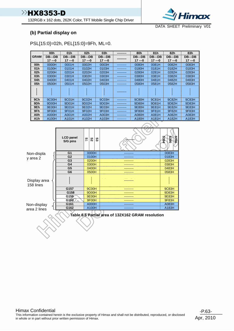
-P.63- Himax Confidential
Apr, 2010
This information contained herein is the exclusive property of Himax and shall not be distributed, reproduced, or disclosed in whole or in part without prior written permission of Himax.
HX8353-D 132RGB x 162 dots, 262K Color, TFT Mobile Single Chip Driver DATA SHEET Preliminary V01
(b) Partial display on PSL[15:0]=02h, PEL[15:0]=9Fh, ML=0.
00h 01h 02h 03h --------- 80h 81h 82h 83h GRAM
DB---DB 17 ---0
DB---DB 17 ---0
DB---DB 17 ---0
DB---DB 17 ---0 --------- DB---DB
17 ---0 DB---DB 17 ---0
DB---DB 17 ---0
DB---DB 17 ---0
00h 0000H 0001H 0002H 0003H --------- 0080H 0081H 0082H 0083H 01h 0100H 0101H 0102H 0103H --------- 0180H 0181H 0182H 0183H 02h 0200H 0201H 0202H 0203H --------- 0280H 0281H 0282H 0283H 03h 0300H 0301H 0302H 0303H --------- 0380H 0381H 0382H 0383H 04h 0400H 0401H 0402H 0403H --------- 0480H 0481H 0482H 0483H 05h 0500H 0501H 0502H 0503H --------- 0580H 0581H 0582H 0583H
-------
-------
-------
-------
-------
--------- -------
-------
-------
-------
9Ch 9C00H 9C01H 9C02H 9C03H --------- 9C80H 9C81H 9C82H 9C83H 9Dh 9D00H 9D01H 9D02H 9D03H --------- 9D80H 9D81H 9D82H 9D83H 9Eh 9E00H 9E01H 9E02H 9E03H --------- 9E80H 9E81H 9E82H 9E83H 9Fh 9F00H 9F01H 9F02H 9F03H --------- 9F80H 9F81H 9F82H 9F83H A0h A000H A001H A002H A003H --------- A080H A081H A082H A083H A1h A100H A101H A102H A103H --------- A180H A181H A182H A183H
Table 6.6 Partial area of 132X162 GRAM resolution
LCD panel S/G pins
S
1
S2
S3 ---------
S394
S395
S396
G1 0000H --------- 0083H G2 0100H --------- 0183H G3 0200H --------- 0283H G4 0300H --------- 0383H G5 0400H --------- 0483H G6 0500H --------- 0583H
-------
-------
---------
-------
G157 9C00H --------- 9C83H G158 9D00H --------- 9D83H G159 9E00H --------- 9E83H G160 9F00H --------- 9F83H G161 A000H --------- A083H G162 A100H --------- A183H
Non-display area 2 lines
Display area 158 lines
Non-display area 2 lines

-P.64- Himax Confidential
Apr, 2010
This information contained herein is the exclusive property of Himax and shall not be distributed, reproduced, or disclosed in whole or in part without prior written permission of Himax.
HX8353-D 132RGB x 162 dots, 262K Color, TFT Mobile Single Chip Driver DATA SHEET Preliminary V01
6.3.8.2 132X162 GRAM resolution (size) (display res olution 128RGB x 160 (RSO[2:0]=3’b000 & STE_SEL=1)
(a) Normal display on In this mode, contents of the frame memory within an area where column pointer is 00h to 83h and page pointer is 00h to A1h is displayed. To display a dot on leftmost top corner, store the dot data at (column pointer, row pointer) = (0, 0).
00h 01h 02h 03h --------- 80h 81h 82h 83h
GRAM
DB---DB 17 ---0
DB---DB 17 ---0
DB---DB 17 ---0
DB---DB 17 ---0 --------- DB---DB
17 ---0 DB---DB 17 ---0
DB---DB 17 ---0
DB---DB 17 ---0
00h 0000H 0001H 0002H 0003H --------- 0080H 0081H 0082H 0083H 01h 0100H 0101H 0102H 0103H --------- 0180H 0181H 0182H 0183H 02h 0200H 0201H 0202H 0203H --------- 0280H 0281H 0282H 0283H 03h 0300H 0301H 0302H 0303H --------- 0380H 0381H 0382H 0383H 04h 0400H 0401H 0402H 0403H --------- 0480H 0481H 0482H 0483H 05h 0500H 0501H 0502H 0503H --------- 0580H 0581H 0582H 0583H
-------
-------
-------
-------
------- ---------
-------
-------
-------
-------
9Ch 9C00H 9C01H 9C02H 9C03H --------- 9C80H 9C81H 9C82H 9C83H 9Dh 9D00H 9D01H 9D02H 9D03H --------- 9D80H 9D81H 9D82H 9D83H 9Eh 9E00H 9E01H 9E02H 9E03H --------- 9E80H 9E81H 9E82H 9E83H 9Fh 9F00H 9F01H 9F02H 9F03H --------- 9F80H 9F81H 9F82H 9F83H A0h A000H A001H A002H A003H --------- A080H A081H A082H A083H A1h A100H A101H A102H A103H --------- A180H A181H A182H A183H
Table 6.7 132X162 GRAM resolution and 128X160 displ ay resolution
LCD panel S/G pins
S7
S8
S9 ---------
S388
S389
S390
G2 0000H --------- 0181H G3 0100H --------- 0281H G4 0200H --------- 0381H G5 0300H --------- 0481H G6 0400H --------- 0581H G7 0500H --------- 0681H
-------
-------
---------
-------
G158 9C00H --------- 9D81H G159 9D00H --------- 9E81H G160 9E00H --------- 9F81H G161 9F00H --------- A081H

-P.65- Himax Confidential
Apr, 2010
This information contained herein is the exclusive property of Himax and shall not be distributed, reproduced, or disclosed in whole or in part without prior written permission of Himax.
HX8353-D 132RGB x 162 dots, 262K Color, TFT Mobile Single Chip Driver DATA SHEET Preliminary V01
(b) Partial display on PSL[15:0]=03h, PEL[15:0]=9Eh, ML=0.
00h 01h 02h 03h --------- 80h 81h 82h 83h GRAM
DB---DB 17 ---0
DB---DB 17 ---0
DB---DB 17 ---0
DB---DB 17 ---0 --------- DB---DB
17 ---0 DB---DB 17 ---0
DB---DB 17 ---0
DB---DB 17 ---0
00h 0000H 0001H 0002H 0003H --------- 0080H 0081H 0082H 0083H 01h 0100H 0101H 0102H 0103H --------- 0180H 0181H 0182H 0183H 02h 0200H 0201H 0202H 0203H --------- 0280H 0281H 0282H 0283H 03h 0300H 0301H 0302H 0303H --------- 0380H 0381H 0382H 0383H 04h 0400H 0401H 0402H 0403H --------- 0480H 0481H 0482H 0483H 05h 0500H 0501H 0502H 0503H --------- 0580H 0581H 0582H 0583H
-------
-------
-------
-------
-------
--------- -------
-------
-------
-------
9Ch 9C00H 9C01H 9C02H 9C03H --------- 9C80H 9C81H 9C82H 9C83H 9Dh 9D00H 9D01H 9D02H 9D03H --------- 9D80H 9D81H 9D82H 9D83H 9Eh 9E00H 9E01H 9E02H 9E03H --------- 9E80H 9E81H 9E82H 9E83H 9Fh 9F00H 9F01H 9F02H 9F03H --------- 9F80H 9F81H 9F82H 9F83H A0h A000H A001H A002H A003H --------- A080H A081H A082H A083H A1h A100H A101H A102H A103H --------- A180H A181H A182H A183H
Table 6.8 Partial area of 132X162 GRAM resolution a nd 128X160 display resolution
LCD panel S/G pins
S
7
S8
S9 ---------
S388
S389
S390
G2 0102H --------- 0181H G3 0202H --------- 0281H G4 0302H --------- 0381H G5 0402H --------- 0481H G6 0502H --------- 0581H G7 0602H --------- 0681H
-------
-------
---------
-------
G158 9D02H --------- 9D81H G159 9E02H --------- 9E81H G160 9F02H --------- 9F81H G161 A002H --------- A081H
Non-display area 2 lines
Display area 156 lines
Non-display area 2 lines

-P.66- Himax Confidential
Apr, 2010
This information contained herein is the exclusive property of Himax and shall not be distributed, reproduced, or disclosed in whole or in part without prior written permission of Himax.
HX8353-D 132RGB x 162 dots, 262K Color, TFT Mobile Single Chip Driver DATA SHEET Preliminary V01
6.3.8.3 128X128 GRAM resolution (size) (display res olution 128RGB x 128 RSO[2:0]=3’b001)
(a) Normal display on In this mode, contents of the frame memory within an area where column pointer is 00h to 7Fh and page pointer is 00h to 7Fh is displayed. To display a dot on leftmost top corner, store the dot data at (column pointer, row pointer) = (0, 0).
00h 01h 02h 03h --------- 7Fh --------- 81h 82h 83h
GRAM
DB---DB 17 ---0
DB---DB 17 ---0
DB---DB 17 ---0
DB---DB 17 ---0 --------- DB---DB
17 ---0 --------- DB---DB 17 ---0
DB---DB 17 ---0
DB---DB 17 ---0
00h 0000H 0001H 0002H 0003H --------- 007FH --------- 0081H 0082H 0083H 01h 0100H 0101H 0102H 0103H --------- 017FH --------- 0181H 0182H 0183H 02h 0200H 0201H 0202H 0203H --------- 027FH --------- 0281H 0282H 0283H 03h 0300H 0301H 0302H 0303H --------- 037FH --------- 0381H 0382H 0383H 04h 0400H 0401H 0402H 0403H --------- 047FH --------- 0481H 0482H 0483H 05h 0500H 0501H 0502H 0503H --------- 057FH --------- 0581H 0582H 0583H
-------
-------
-------
-------
-------
---------
------- ---------
-------
-------
-------
7Eh 7E00H 7E01H 7E02H 7E03H --------- 7E7FH --------- 7E81H 7E82H 7E83H 7Fh 7F00H 7F01H 7F02H 7F03H --------- 7E7FH --------- 7F81H 7F82H 7F83H
-------
-------
-------
-------
------- ---------
------- ---------
-------
-------
-------
9Ch 9C00H 9C01H 9C02H 9C03H --------- 9C7FH --------- 9C81H 9C82H 9C83H 9Dh 9D00H 9D01H 9D02H 9D03H --------- 9D7FH --------- 9D81H 9D82H 9D83H 9Eh 9E00H 9E01H 9E02H 9E03H --------- 9E7FH --------- 9E81H 9E82H 9E83H 9Fh 9F00H 9F01H 9F02H 9F03H --------- 9F7FH --------- 9F81H 9F82H 9F83H A0h A000H A001H A002H A003H --------- A07FH --------- A081H A082H A083H A1h A100H A101H A102H A103H --------- A17FH --------- A181H A182H A183H
Table 6.9 128X128 GRAM resolution
LCD panel S/G pins
S7
S8
S9 ---------
S388
S389
S390
G2 0000H --------- 007FH G3 0100H --------- 017FH G4 0200H --------- 027FH G5 0300H --------- 037FH G6 0400H --------- 047FH G7 0500H --------- 057FH
-------
-------
---------
-------
G126 7C00H --------- 7C7FH G127 7D00H --------- 7D7FH G128 7E00H --------- 7E7FH G129 7F00H --------- 7F7FH
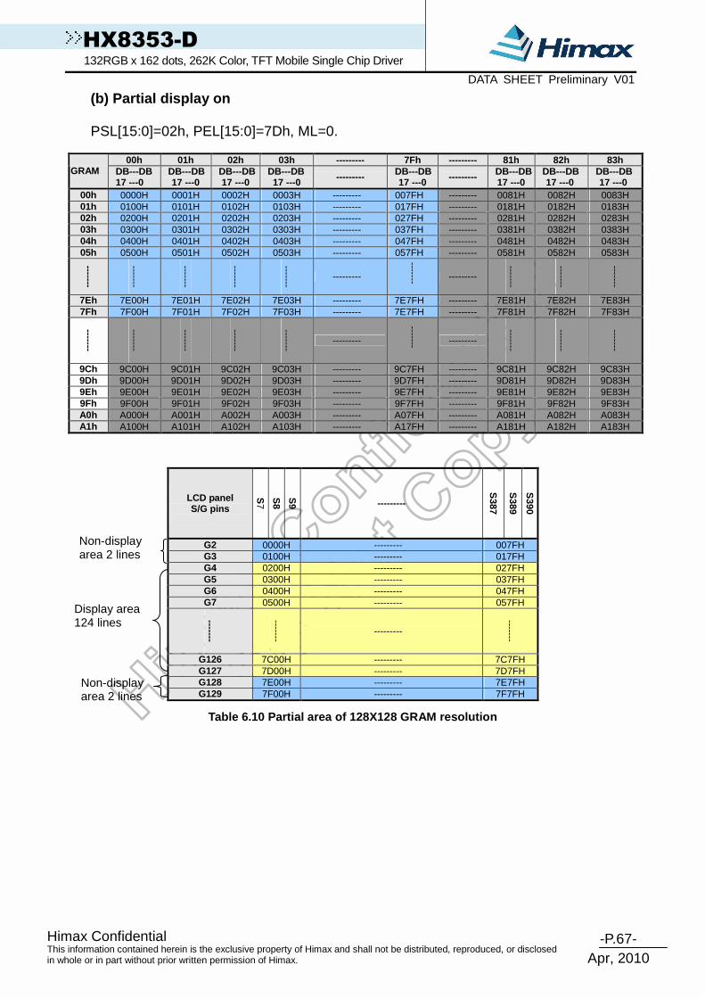
-P.67- Himax Confidential
Apr, 2010
This information contained herein is the exclusive property of Himax and shall not be distributed, reproduced, or disclosed in whole or in part without prior written permission of Himax.
HX8353-D 132RGB x 162 dots, 262K Color, TFT Mobile Single Chip Driver DATA SHEET Preliminary V01
(b) Partial display on PSL[15:0]=02h, PEL[15:0]=7Dh, ML=0.
00h 01h 02h 03h --------- 7Fh --------- 81h 82h 83h
GRAM
DB---DB 17 ---0
DB---DB 17 ---0
DB---DB 17 ---0
DB---DB 17 ---0 --------- DB---DB
17 ---0 --------- DB---DB 17 ---0
DB---DB 17 ---0
DB---DB 17 ---0
00h 0000H 0001H 0002H 0003H --------- 007FH --------- 0081H 0082H 0083H 01h 0100H 0101H 0102H 0103H --------- 017FH --------- 0181H 0182H 0183H 02h 0200H 0201H 0202H 0203H --------- 027FH --------- 0281H 0282H 0283H 03h 0300H 0301H 0302H 0303H --------- 037FH --------- 0381H 0382H 0383H 04h 0400H 0401H 0402H 0403H --------- 047FH --------- 0481H 0482H 0483H 05h 0500H 0501H 0502H 0503H --------- 057FH --------- 0581H 0582H 0583H
-------
-------
-------
-------
-------
---------
------- ---------
-------
-------
-------
7Eh 7E00H 7E01H 7E02H 7E03H --------- 7E7FH --------- 7E81H 7E82H 7E83H 7Fh 7F00H 7F01H 7F02H 7F03H --------- 7E7FH --------- 7F81H 7F82H 7F83H
-------
-------
-------
-------
-------
---------
------- ---------
-------
-------
-------
9Ch 9C00H 9C01H 9C02H 9C03H --------- 9C7FH --------- 9C81H 9C82H 9C83H 9Dh 9D00H 9D01H 9D02H 9D03H --------- 9D7FH --------- 9D81H 9D82H 9D83H 9Eh 9E00H 9E01H 9E02H 9E03H --------- 9E7FH --------- 9E81H 9E82H 9E83H 9Fh 9F00H 9F01H 9F02H 9F03H --------- 9F7FH --------- 9F81H 9F82H 9F83H A0h A000H A001H A002H A003H --------- A07FH --------- A081H A082H A083H A1h A100H A101H A102H A103H --------- A17FH --------- A181H A182H A183H
Table 6.10 Partial area of 128X128 GRAM resolution
LCD panel S/G pins
S7
S8
S9 ---------
S387
S389
S390
G2 0000H --------- 007FH G3 0100H --------- 017FH G4 0200H --------- 027FH G5 0300H --------- 037FH G6 0400H --------- 047FH G7 0500H --------- 057FH
-------
-------
---------
-------
G126 7C00H --------- 7C7FH G127 7D00H --------- 7D7FH G128 7E00H --------- 7E7FH G129 7F00H --------- 7F7FH
Non-display area 2 lines
Display area 124 lines
Non-display area 2 lines

-P.68- Himax Confidential
Apr, 2010
This information contained herein is the exclusive property of Himax and shall not be distributed, reproduced, or disclosed in whole or in part without prior written permission of Himax.
HX8353-D 132RGB x 162 dots, 262K Color, TFT Mobile Single Chip Driver DATA SHEET Preliminary V01
6.3.8.4 120X160 GRAM resolution (size) (display res olution 120RGB x 160 RSO[2:0]=3’b010)
(a) Normal display on In this mode, contents of the frame memory within an area where column pointer is 00h to 77h and page pointer is 00h to 9Fh is displayed. To display a dot on leftmost top corner, store the dot data at (column pointer, row pointer) = (0, 0).
00h 01h 02h 03h --------- 77h --------- 81h 82h 83h
GRAM
DB---DB 17 ---0
DB---DB 17 ---0
DB---DB 17 ---0
DB---DB 17 ---0 --------- DB---DB
17 ---0 --------- DB---DB 17 ---0
DB---DB 17 ---0
DB---DB 17 ---0
00h 0000H 0001H 0002H 0003H --------- 0077H --------- 0081H 0082H 0083H 01h 0100H 0101H 0102H 0103H --------- 0177H --------- 0181H 0182H 0183H 02h 0200H 0201H 0202H 0203H --------- 0277H --------- 0281H 0282H 0283H 03h 0300H 0301H 0302H 0303H --------- 0377H --------- 0381H 0382H 0383H 04h 0400H 0401H 0402H 0403H --------- 0477H --------- 0481H 0482H 0483H 05h 0500H 0501H 0502H 0503H --------- 0577H --------- 0581H 0582H 0583H
-------
-------
-------
-------
-------
---------
------- ---------
-------
-------
-------
9Ch 9C00H 9C01H 9C02H 9C03H --------- 9C77H --------- 9C81H 9C82H 9C83H 9Dh 9D00H 9D01H 9D02H 9D03H --------- 9D77H --------- 9D81H 9D82H 9D83H 9Eh 9E00H 9E01H 9E02H 9E03H --------- 9E77H --------- 9E81H 9E82H 9E83H 9Fh 9F00H 9F01H 9F02H 9F03H --------- 9F77H --------- 9F81H 9F82H 9F83H A0h A000H A001H A002H A003H --------- A077H --------- A081H A082H A083H A1h A100H A101H A102H A103H --------- A177H --------- A181H A182H A183H
Table 6.11 120X160 GRAM resolution
LCD panel S/G pins
S7
S8
S9 ---------
S364
S365
S366
G2 0000H --------- 0077H G3 0100H --------- 0177H G4 0200H --------- 0277H G5 0300H --------- 0377H G6 0400H --------- 0477H G7 0500H --------- 0577H
-------
-------
---------
-------
G158 9C00H --------- 9C77H G159 9D00H --------- 9D77H G160 9E00H --------- 9E77H G161 9F00H --------- 9F77H

-P.69- Himax Confidential
Apr, 2010
This information contained herein is the exclusive property of Himax and shall not be distributed, reproduced, or disclosed in whole or in part without prior written permission of Himax.
HX8353-D 132RGB x 162 dots, 262K Color, TFT Mobile Single Chip Driver DATA SHEET Preliminary V01
(b) Partial display on PSL[15:0]=02h, PEL[15:0]=9Dh, ML=0.
00h 01h 02h 03h --------- 77h --------- 81h 82h 83h
GRAM
DB---DB 17 ---0
DB---DB 17 ---0
DB---DB 17 ---0
DB---DB 17 ---0 --------- DB---DB
17 ---0 --------- DB---DB 17 ---0
DB---DB 17 ---0
DB---DB 17 ---0
00h 0000H 0001H 0002H 0003H --------- 0077H --------- 0081H 0082H 0083H 01h 0100H 0101H 0102H 0103H --------- 0177H --------- 0181H 0182H 0183H 02h 0200H 0201H 0202H 0203H --------- 0277H --------- 0281H 0282H 0283H 03h 0300H 0301H 0302H 0303H --------- 0377H --------- 0381H 0382H 0383H 04h 0400H 0401H 0402H 0403H --------- 0477H --------- 0481H 0482H 0483H 05h 0500H 0501H 0502H 0503H --------- 0577H --------- 0581H 0582H 0583H
-------
-------
-------
-------
-------
---------
------- ---------
-------
-------
-------
9Ch 9C00H 9C01H 9C02H 9C03H --------- 9C77H --------- 9C81H 9C82H 9C83H 9Dh 9D00H 9D01H 9D02H 9D03H --------- 9D77H --------- 9D81H 9D82H 9D83H 9Eh 9E00H 9E01H 9E02H 9E03H --------- 9E77H --------- 9E81H 9E82H 9E83H 9Fh 9F00H 9F01H 9F02H 9F03H --------- 9F77H --------- 9F81H 9F82H 9F83H A0h A000H A001H A002H A003H --------- A077H --------- A081H A082H A083H A1h A100H A101H A102H A103H --------- A177H --------- A181H A182H A183H
Table 6.12 Partial area of 120X160 GRAM resolution
LCD panel S/G pins
S
7
S8
S9 ---------
S364
S365
S366
G2 0000H --------- 0077H G3 0100H --------- 0177H G4 0200H --------- 0277H G5 0300H --------- 0377H G6 0400H --------- 0477H G7 0500H --------- 0577H
-------
-------
---------
-------
G158 9C00H --------- 9C77H G159 9D00H --------- 9D77H G160 9E00H --------- 9E77H G161 9F00H --------- 9F77H
Non-display area 2 lines
Display area 156 lines
Non-display area 2 lines

-P.70- Himax Confidential
Apr, 2010
This information contained herein is the exclusive property of Himax and shall not be distributed, reproduced, or disclosed in whole or in part without prior written permission of Himax.
HX8353-D 132RGB x 162 dots, 262K Color, TFT Mobile Single Chip Driver DATA SHEET Preliminary V01
6.3.8.5 128X160 GRAM resolution (size) (display res olution 128RGB x 160 (RSO[2:0]=3’b011)
(a) Normal display on In this mode, contents of the frame memory within an area where column pointer is 00h to 7Fh and page pointer is 00h to 9Fh is displayed. To display a dot on leftmost top corner, store the dot data at (column pointer, row pointer) = (0, 0).
00h 01h 02h 03h --------- 7Fh 80h 81h 82h 83h
GRAM
DB---DB 17 ---0
DB---DB 17 ---0
DB---DB 17 ---0
DB---DB 17 ---0 --------- DB---DB
17 ---0 DB---DB 17 ---0
DB---DB 17 ---0
DB---DB 17 ---0
DB---DB 17 ---0
00h 0000H 0001H 0002H 0003H --------- 007FH 0080H 0081H 0082H 0083H 01h 0100H 0101H 0102H 0103H --------- 017FH 0180H 0181H 0182H 0183H 02h 0200H 0201H 0202H 0203H --------- 027FH 0280H 0281H 0282H 0283H 03h 0300H 0301H 0302H 0303H --------- 037FH 0380H 0381H 0382H 0383H 04h 0400H 0401H 0402H 0403H --------- 047FH 0480H 0481H 0482H 0483H 05h 0500H 0501H 0502H 0503H --------- 057FH 0580H 0581H 0582H 0583H
-------
-------
-------
-------
-------
---------
-------
-------
-------
-------
-------
9Ch 9C00H 9C01H 9C02H 9C03H --------- 9C7FH 9C80H 9C81H 9C82H 9C83H 9Dh 9D00H 9D01H 9D02H 9D03H --------- 9D7FH 9D80H 9D81H 9D82H 9D83H 9Eh 9E00H 9E01H 9E02H 9E03H --------- 9E7FH 9E80H 9E81H 9E82H 9E83H 9Fh 9F00H 9F01H 9F02H 9F03H --------- 9F7FH 9F80H 9F81H 9F82H 9F83H A0h A000H A001H A002H A003H --------- A07FH A080H A081H A082H A083H A1h A100H A101H A102H A103H --------- A17FH A180H A181H A182H A183H
Table 6.13 128X160 GRAM resolution
LCD panel S/G pins
S7
S8
S9 ---------
S388
S389
S390
G2 0000H --------- 007FH G3 0100H --------- 017FH G4 0200H --------- 027FH G5 0300H --------- 037FH G6 0400H --------- 047FH G7 0500H --------- 057FH
-------
-------
---------
-------
G158 9C00H --------- 9C7FH G159 9D00H --------- 9D7FH G160 9E00H --------- 9E7FH G161 9F00H --------- 9F7FH

-P.71- Himax Confidential
Apr, 2010
This information contained herein is the exclusive property of Himax and shall not be distributed, reproduced, or disclosed in whole or in part without prior written permission of Himax.
HX8353-D 132RGB x 162 dots, 262K Color, TFT Mobile Single Chip Driver DATA SHEET Preliminary V01
(b) Partial display on PSL[15:0]=02h, PEL[15:0]=9Dh, ML=0.
00h 01h 02h 03h --------- 7Fh 80h 81h 82h 83h
GRAM
DB---DB 17 ---0
DB---DB 17 ---0
DB---DB 17 ---0
DB---DB 17 ---0 --------- DB---DB
17 ---0 DB---DB 17 ---0
DB---DB 17 ---0
DB---DB 17 ---0
DB---DB 17 ---0
00h 0000H 0001H 0002H 0003H --------- 007FH 0080H 0081H 0082H 0083H 01h 0100H 0101H 0102H 0103H --------- 017FH 0180H 0181H 0182H 0183H 02h 0200H 0201H 0202H 0203H --------- 027FH 0280H 0281H 0282H 0283H 03h 0300H 0301H 0302H 0303H --------- 037FH 0380H 0381H 0382H 0383H 04h 0400H 0401H 0402H 0403H --------- 047FH 0480H 0481H 0482H 0483H 05h 0500H 0501H 0502H 0503H --------- 057FH 0580H 0581H 0582H 0583H
-------
-------
-------
-------
-------
---------
-------
-------
-------
-------
-------
9Ch 9C00H 9C01H 9C02H 9C03H --------- 9C7FH 9C80H 9C81H 9C82H 9C83H 9Dh 9D00H 9D01H 9D02H 9D03H --------- 9D7FH 9D80H 9D81H 9D82H 9D83H 9Eh 9E00H 9E01H 9E02H 9E03H --------- 9E7FH 9E80H 9E81H 9E82H 9E83H 9Fh 9F00H 9F01H 9F02H 9F03H --------- 9F7FH 9F80H 9F81H 9F82H 9F83H A0h A000H A001H A002H A003H --------- A07FH A080H A081H A082H A083H A1h A100H A101H A102H A103H --------- A17FH A180H A181H A182H A183H
Table 6.14 Partial area of 128X160 GRAM resolution
LCD panel S/G pins
S
7
S8
S9 ---------
S388
S389
S390
G2 0000H --------- 007FH G3 0100H --------- 017FH G4 0200H --------- 027FH G5 0300H --------- 037FH G6 0400H --------- 047FH G7 0500H --------- 057FH
-------
-------
---------
-------
G158 9C00H --------- 9C7FH G159 9D00H --------- 9D7FH G160 9E00H --------- 9E7FH G161 9F00H --------- 9F7FH
Non-display area 2 lines
Display area 156 lines
Non-display area 2 lines

-P.72- Himax Confidential
Apr, 2010
This information contained herein is the exclusive property of Himax and shall not be distributed, reproduced, or disclosed in whole or in part without prior written permission of Himax.
HX8353-D 132RGB x 162 dots, 262K Color, TFT Mobile Single Chip Driver DATA SHEET Preliminary V01
6.3.8.6 96x68 Resolution (RSO[2:0]=3’b100)
(a) Normal display on In this mode, contents of the frame memory within an area where column pointer is 00h to 5Fh and page pointer is 00h to 43h is displayed. To display a dot on leftmost top corner, store the dot data at (column pointer, row pointer) = (0, 0).
00h 01h 02h 03h --- 5Dh 5Eh 5Fh --- 80h 81h 82h 83h
GRAM
DB---DB 17 ---0
DB---DB 17 ---0
DB---DB 17 ---0
DB---DB 17 ---0
--- DB---DB 17 ---0
DB---DB 17 ---0
DB---DB 17 ---0
--- DB---DB 17 ---0
DB---DB 17 ---0
DB---DB 17 ---0
DB---DB 17 ---0
00h 0000H 0001H 0002H 0003H --- 005DH 005EH 005FH --- 0080H 0081H 0082H 0083H 01h 0100H 0101H 0102H 0103H --- 015DH 015EH 015FH --- 0180H 0181H 0182H 0183H 02h 0200H 0201H 0202H 0203H --- 025DH 025EH 025FH --- 0280H 0281H 0282H 0283H 03h 0300H 0301H 0302H 0303H --- 035DH 035EH 035FH --- 0380H 0381H 0382H 0383H 04h 0400H 0401H 0402H 0403H --- 045DH 045EH 045FH --- 0480H 0481H 0482H 0483H 05h 0500H 0501H 0502H 0503H --- 055DH 055EH 055FH --- 0580H 0581H 0582H 0583H
-------
-------
-------
-------
-------
---
-------
-------
-------
---
-------
-------
-------
-------
41h 4100H 4101H 4102H 4103H --- 415DH 415EH 415FH --- 4180H 4181H 4182H 4183H 42h 4200H 4201H 4102H 4103H --- 425DH 425EH 425FH --- 4280H 4281H 4282H 4283H 43h 4300H 4301H 4302H 4303H --- 435DH 435EH 435FH --- 4380H 4381H 4382H 4383H
-------
-------
-------
-------
-------
---
-------
-------
-------
---
-------
-------
-------
-------
9Ch 9C00H 9C01H 9C02H 9C03H --- 9C5DH 9C5EH 9C5FH --- 9C80H 9C81H 9C82H 9C83H 9Dh 9D00H 9D01H 9D02H 9D03H --- 9D5DH 9D5EH 9D5FH --- 9D80H 9D81H 9D82H 9D83H 9Eh 9E00H 9E01H 9E02H 9E03H --- 9E5DH 9E5EH 9E5FH --- 9E80H 9E81H 9E82H 9E83H 9Fh 9F00H 9F01H 9F02H 9F03H --- 9F5DH 9F5EH 9F5FH --- 9F80H 9F81H 9F82H 9F83H A0h A000H A001H A002H A003H --- A05DH A05EH A05FH --- A080H A081H A082H A083H A1h A100H A101H A102H A103H --- A15DH A15EH A15FH --- A180H A181H A182H A183H
Table 6.15 96X68 GRAM resolution
LCD panel S/G pins
S55
S56
S57
S340
S341
S342
G1 0000H --------- 005FH G2 0100H --------- 015FH G3 0200H --------- 025FH G4 0300H --------- 035FH G5 0400H --------- 045FH G6 0500H --------- 055FH
-------
-------
-------
-------
G67 4200H --------- 425FH G68 4300H --------- 435FH

-P.73- Himax Confidential
Apr, 2010
This information contained herein is the exclusive property of Himax and shall not be distributed, reproduced, or disclosed in whole or in part without prior written permission of Himax.
HX8353-D 132RGB x 162 dots, 262K Color, TFT Mobile Single Chip Driver DATA SHEET Preliminary V01
(b) Partial display on PSL[15:0]=02, PEL[15:0]=41, ML=0.
00h 01h 02h 03h --- 5Dh 5Eh 5Fh --- 80h 81h 82h 83h
GRAM
DB---DB 17 ---0
DB---DB 17 ---0
DB---DB 17 ---0
DB---DB 17 ---0
--- DB---DB 17 ---0
DB---DB 17 ---0
DB---DB 17 ---0
--- DB---DB 17 ---0
DB---DB 17 ---0
DB---DB 17 ---0
DB---DB 17 ---0
00h 0000H 0001H 0002H 0003H --- 005DH 005EH 005FH --- 0080H 0081H 0082H 0083H 01h 0100H 0101H 0102H 0103H --- 015DH 015EH 015FH --- 0180H 0181H 0182H 0183H 02h 0200H 0201H 0202H 0203H --- 025DH 025EH 025FH --- 0280H 0281H 0282H 0283H 03h 0300H 0301H 0302H 0303H --- 035DH 035EH 035FH --- 0380H 0381H 0382H 0383H 04h 0400H 0401H 0402H 0403H --- 045DH 045EH 045FH --- 0480H 0481H 0482H 0483H 05h 0500H 0501H 0502H 0503H --- 055DH 055EH 055FH --- 0580H 0581H 0582H 0583H
-------
-------
-------
-------
-------
---
-------
-------
------- ---
-------
-------
-------
-------
41h 4100H 4101H 4102H 4103H --- 415DH 415EH 415FH --- 4180H 4181H 4182H 4183H 42h 4200H 4201H 4202H 4203H --- 425DH 425EH 425FH --- 4280H 4281H 4282H 4283H 43h 4300H 4301H 4302H 4303H --- 435DH 435EH 435FH --- 4380H 4381H 4382H 4383H
-------
-------
-------
-------
-------
---
-------
-------
-------
---
-------
-------
-------
-------
9Ch 9C00H 9C01H 9C02H 9C03H --- 9C5DH 9C5EH 9C5FH --- 9C80H 9C81H 9C82H 9C83H 9Dh 9D00H 9D01H 9D02H 9D03H --- 9D5DH 9D5EH 9D5FH --- 9D80H 9D81H 9D82H 9D83H 9Eh 9E00H 9E01H 9E02H 9E03H --- 9E5DH 9E5EH 9E5FH --- 9E80H 9E81H 9E82H 9E83H 9Fh 9F00H 9F01H 9F02H 9F03H --- 9F5DH 9F5EH 9F5FH --- 9F80H 9F81H 9F82H 9F83H A0h A000H A001H A002H A003H --- A05DH A05EH A05FH --- A080H A081H A082H A083H A1h A100H A101H A102H A103H --- A15DH A15EH A15FH --- A180H A181H A182H A183H
Table 6.16 Partial area of 96X68 GRAM resolution
LCD panel S/G pins
S55
S56
S57
S340
S341
S342
G1 0000H --------- 005FH G2 0100H --------- 015FH G3 0200H --------- 025FH G4 0300H --------- 035FH G5 0400H --------- 045FH G6 0500H --------- 055FH
-------
-------
-------
-------
G66 4100H --------- 415FH G67 4200H --------- 425FH G68 4300H --------- 435FH
Non-display area 2 lines
Non-display area 2 lines
Display area 64 lines
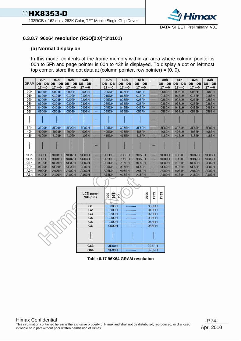
-P.74- Himax Confidential
Apr, 2010
This information contained herein is the exclusive property of Himax and shall not be distributed, reproduced, or disclosed in whole or in part without prior written permission of Himax.
HX8353-D 132RGB x 162 dots, 262K Color, TFT Mobile Single Chip Driver DATA SHEET Preliminary V01
6.3.8.7 96x64 resolution (RSO[2:0]=3’b101)
(a) Normal display on In this mode, contents of the frame memory within an area where column pointer is 00h to 5Fh and page pointer is 00h to 43h is displayed. To display a dot on leftmost top corner, store the dot data at (column pointer, row pointer) = (0, 0).
00h 01h 02h 03h --- 5Dh 5Eh 5Fh --- 80h 81h 82h 83h
GRAM
DB---DB 17 ---0
DB---DB 17 ---0
DB---DB 17 ---0
DB---DB 17 ---0
--- DB---DB 17 ---0
DB---DB 17 ---0
DB---DB 17 ---0
--- DB---DB 17 ---0
DB---DB 17 ---0
DB---DB 17 ---0
DB---DB 17 ---0
00h 0000H 0001H 0002H 0003H --- 005DH 005EH 005FH --- 0080H 0081H 0082H 0083H 01h 0100H 0101H 0102H 0103H --- 015DH 015EH 015FH --- 0180H 0181H 0182H 0183H 02h 0200H 0201H 0202H 0203H --- 025DH 025EH 025FH --- 0280H 0281H 0282H 0283H 03h 0300H 0301H 0302H 0303H --- 035DH 035EH 035FH --- 0380H 0381H 0382H 0383H 04h 0400H 0401H 0402H 0403H --- 045DH 045EH 045FH --- 0480H 0481H 0482H 0483H 05h 0500H 0501H 0502H 0503H --- 055DH 055EH 055FH --- 0580H 0581H 0582H 0583H
-------
-------
-------
-------
-------
---
-------
-------
-------
---
-------
-------
-------
-------
3Fh 3F00H 3F01H 3F02H 3F03H --- 3F5DH 3F5EH 3F5FH --- 3F80H 3F81H 3F82H 3F83H 40h 4000H 4001H 4002H 4003H --- 405DH 405EH 405FH --- 4080H 4081H 4082H 4083H 41h 4100H 4101H 4102H 4103H --- 415DH 415EH 415FH --- 4180H 4181H 4182H 4183H
-------
-------
-------
-------
-------
---
-------
-------
-------
---
-------
-------
-------
-------
9Ch 9C00H 9C01H 9C02H 9C03H --- 9C5DH 9C5EH 9C5FH --- 9C80H 9C81H 9C82H 9C83H 9Dh 9D00H 9D01H 9D02H 9D03H --- 9D5DH 9D5EH 9D5FH --- 9D80H 9D81H 9D82H 9D83H 9Eh 9E00H 9E01H 9E02H 9E03H --- 9E5DH 9E5EH 9E5FH --- 9E80H 9E81H 9E82H 9E83H 9Fh 9F00H 9F01H 9F02H 9F03H --- 9F5DH 9F5EH 9F5FH --- 9F80H 9F81H 9F82H 9F83H A0h A000H A001H A002H A003H --- A05DH A05EH A05FH --- A080H A081H A082H A083H A1h A100H A101H A102H A103H --- A15DH A15EH A15FH --- A180H A181H A182H A183H
Table 6.17 96X64 GRAM resolution
LCD panel S/G pins
S55
S56
S57
S340
S341
S342
G1 0000H --------- 005FH G2 0100H --------- 015FH G3 0200H --------- 025FH G4 0300H --------- 035FH G5 0400H --------- 045FH G6 0500H --------- 055FH
-------
-------
-------
-------
G63 3E00H --------- 3E5FH G64 3F00H --------- 3F5FH

-P.75- Himax Confidential
Apr, 2010
This information contained herein is the exclusive property of Himax and shall not be distributed, reproduced, or disclosed in whole or in part without prior written permission of Himax.
HX8353-D 132RGB x 162 dots, 262K Color, TFT Mobile Single Chip Driver DATA SHEET Preliminary V01
(b) Partial display on PSL[15:0]=02, PEL[15:0]=3D, ML=0.
00h 01h 02h 03h --- 5Dh 5Eh 5Fh --- 80h 81h 82h 83h
GRAM
DB---DB 17 ---0
DB---DB 17 ---0
DB---DB 17 ---0
DB---DB 17 ---0
--- DB---DB 17 ---0
DB---DB 17 ---0
DB---DB 17 ---0
--- DB---DB 17 ---0
DB---DB 17 ---0
DB---DB 17 ---0
DB---DB 17 ---0
00h 0000H 0001H 0002H 0003H --- 005DH 005EH 005FH --- 0080H 0081H 0082H 0083H 01h 0100H 0101H 0102H 0103H --- 015DH 015EH 015FH --- 0180H 0181H 0182H 0183H 02h 0200H 0201H 0202H 0203H --- 025DH 025EH 025FH --- 0280H 0281H 0282H 0283H 03h 0300H 0301H 0302H 0303H --- 035DH 035EH 035FH --- 0380H 0381H 0382H 0383H 04h 0400H 0401H 0402H 0403H --- 045DH 045EH 045FH --- 0480H 0481H 0482H 0483H 05h 0500H 0501H 0502H 0503H --- 055DH 055EH 055FH --- 0580H 0581H 0582H 0583H
-------
-------
-------
-------
-------
---
-------
-------
-------
---
-------
-------
-------
-------
3Fh 3F00H 3F01H 3F02H 3F03H --- 3F5DH 3F5EH 3F5FH --- 3F80H 3F81H 3F82H 3F83H 40h 4000H 4001H 4002H 4003H --- 405DH 405EH 405FH --- 4080H 4081H 4082H 4083H 41h 4100H 4101H 4102H 4103H --- 415DH 415EH 415FH --- 4180H 4181H 4182H 4183H
-------
-------
-------
-------
-------
---
-------
-------
-------
---
-------
-------
-------
-------
9Ch 9C00H 9C01H 9C02H 9C03H --- 9C5DH 9C5EH 9C5FH --- 9C80H 9C81H 9C82H 9C83H 9Dh 9D00H 9D01H 9D02H 9D03H --- 9D5DH 9D5EH 9D5FH --- 9D80H 9D81H 9D82H 9D83H 9Eh 9E00H 9E01H 9E02H 9E03H --- 9E5DH 9E5EH 9E5FH --- 9E80H 9E81H 9E82H 9E83H 9Fh 9F00H 9F01H 9F02H 9F03H --- 9F5DH 9F5EH 9F5FH --- 9F80H 9F81H 9F82H 9F83H A0h A000H A001H A002H A003H --- A05DH A05EH A05FH --- A080H A081H A082H A083H A1h A100H A101H A102H A103H --- A15DH A15EH A15FH --- A180H A181H A182H A183H
Table 6.18 Partial area of 96X64 GRAM resolution
LCD panel S/G pins
S55
S56
S57
S340
S341
S342
G1 0000H --------- 005FH G2 0100H --------- 015FH G3 0200H --------- 025FH G4 0300H --------- 035FH G5 0400H --------- 045FH G6 0500H --------- 055FH
-------
-------
-------
-------
G63 3E00H --------- 3E5FH G64 3F00H --------- 3F5FH
Non-display area 2 lines
Non-display area 2 lines
Display area 60 lines

-P.76- Himax Confidential
Apr, 2010
This information contained herein is the exclusive property of Himax and shall not be distributed, reproduced, or disclosed in whole or in part without prior written permission of Himax.
HX8353-D 132RGB x 162 dots, 262K Color, TFT Mobile Single Chip Driver DATA SHEET Preliminary V01
6.4 Vertical scrolling display
The vertical scrolling display is specified by SCRLAR instruction (R33h) and VSCSAD instruction (R37h). The Vertical scrolling is only enable when using 132 x 162 GRAM resolution, display resolution 132RGB x 162 (RSO[2:0]=3’b000 & STE_SEL=0) and display resolution 128RGB x 160 (RSO[2:0]=3’b011)
Figure 6.12 Vertical scrolling display
Original
Scrolling
TFA
VSA
BFA

-P.77- Himax Confidential
Apr, 2010
This information contained herein is the exclusive property of Himax and shall not be distributed, reproduced, or disclosed in whole or in part without prior written permission of Himax.
HX8353-D 132RGB x 162 dots, 262K Color, TFT Mobile Single Chip Driver DATA SHEET Preliminary V01
When RSO[2:0]=3’b000(132RGB x 162) and Vertical Scrolling Definition Parameters (TFA+VSA+BFA)=162 (other setting is prohibited). In this case, scrolling is applied as shown below. Example 1: RSO=3’b000(132RGB x 162), TFA =3, VSA=15 7, BFA=2, VSP=4, MADCTR(ML)=0: Scrolling
00000000hhhh 01010101hhhh 02020202hhhh 03030303hhhh 80808080hhhh 81818181hhhh 82828282hhhh 83838383hhhh
00000000hhhh
01010101hhhh
02020202hhhh
03030303hhhh
04040404hhhh
9999DhDhDhDh
9999EhEhEhEh
9999FhFhFhFh
AAAA0000hhhh
00000000 01010101 02020202 03030303 04040404
13131313121212121111111110101010
20202020
30303030
40404040
WWWW0000
XXXX0000
YYYY0000
22222222
XXXX2222
YYYY2222
ZZZZ2222
21212121
31313131
WWWW1111
XXXX1111
YYYY1111
ZZZZ1111
YYYY3333
ZZZZ3333
1111WWWW
0000XXXX 0000YYYY 0000ZZZZ
1111ZZZZ
2222ZZZZ
3333ZZZZ
4444ZZZZ
VZVZVZVZ
WZWZWZWZ
XZXZXZXZ
YZYZYZYZ
ZZZZZZZZZYZYZYZYZXZXZXZXZWZWZWZWZZZZ4444
0000WWWW
1111XXXX 1111YYYY
2222YYYY
3333YYYY
WYWYWYWY
XYXYXYXY
YYYYYYYY
2222XXXX
XXXXXXXX
YXYXYXYX
ZVZVZVZV
YWYWYWYW
0000VVVV
9999ChChChCh
VVVV0000
1111stststst
2222ndndndnd
3333ndndndnd
160160160160thththth
4444thththth
5555thththth05050505hhhh 50505050 5555ZZZZ
AAAA1111hhhh ZZZZ0000 ZZZZ5555
05050505
04040404hhhh
14141414
23232323
32323232
41414141 4444YYYY
UUUU0000 UZUZUZUZ
VVVV1111 VYVYVYVY
156156156156thththth
157157157157thththth
158158158158thththth
159159159159thththth
161161161161thththth
162162162162thththth
0000
1111
2222
3333
4444
5555
156156156156
157157157157
158158158158
159159159159
160160160160
161161161161
Scan order
Scan Address
TFA
VSA
BFA
GGGG1111
GGGG2222
GGGG3333
GGGG4444
GGGG5555
00000000 01010101 02020202 03030303 04040404
13131313121212121111111110101010
20202020
30303030
40404040
WWWW0000
XXXX0000
YYYY0000
22222222
XXXX2222
YYYY2222
ZZZZ2222
21212121
31313131
WWWW1111
XXXX1111
YYYY1111
ZZZZ1111
YYYY3333
ZZZZ3333
1111WWWW
0000XXXX 0000YYYY 0000ZZZZ
1111ZZZZ
2222ZZZZ
3333ZZZZ
4444ZZZZ
VZVZVZVZ
WZWZWZWZ
XZXZXZXZ
YZYZYZYZ
ZZZZZZZZZYZYZYZYZXZXZXZXZWZWZWZWZZZZ4444
0000WWWW
1111XXXX 1111YYYY
2222YYYY
3333YYYY
WYWYWYWY
XYXYXYXY
YYYYYYYY
2222XXXX
XXXXXXXX
YXYXYXYX
ZVZVZVZV
YWYWYWYW
0000VVVV
VVVV0000
GGGG6666
50505050 5555ZZZZ
ZZZZ0000 ZZZZ5555
05050505
14141414
23232323
32323232
41414141 4444YYYY
VVVV1111 VYVYVYVY
GGGG158158158158
GGGG159159159159
GGGG160160160160
GGGG161161161161
GGGG157157157157
GGGG162162162162
TFA
Scroll area = 157 lines
BFA
51515151 5555YYYY
60606060 6666ZZZZ
42424242 4444XXXX
3333XXXX
VSP
132 x 162 x 18 bitFrame memory
132 x 162 LCD Panel
SS SS33 3399 9966 66
SS SS11 11
Figure 6.13 Example1 of scrolling
Example 2: RSO=3’b000(132RGB x 162), TFA =3, VSA=15 7, BFA=2, VSP=4, MADCTR (ML)=1: Scrolling (TFA and BFA ar e exchanged)
00000000hhhh 01010101hhhh 02020202hhhh 03030303hhhh 80808080hhhh 81818181hhhh 82828282hhhh 83838383hhhh
00000000hhhh
01010101hhhh
02020202hhhh
03030303hhhh
04040404hhhh
9999DhDhDhDh
9999EhEhEhEh
9999FhFhFhFh
AAAA0000hhhh
00000000 01010101 02020202 03030303 04040404
13131313121212121111111110101010
20202020
30303030
40404040
WWWW0000
XXXX0000
YYYY0000
22222222
XXXX2222
YYYY2222
ZZZZ2222
21212121
31313131
WWWW1111
XXXX1111
YYYY1111
ZZZZ1111
YYYY3333
ZZZZ3333
1111WWWW
0000XXXX 0000YYYY 0000ZZZZ
1111ZZZZ
2222ZZZZ
3333ZZZZ
4444ZZZZ
VZVZVZVZ
WZWZWZWZ
XZXZXZXZ
YZYZYZYZ
ZZZZZZZZZYZYZYZYZXZXZXZXZWZWZWZWZZZZ4444
0000WWWW
1111XXXX 1111YYYY
2222YYYY
3333YYYY
WYWYWYWY
XYXYXYXY
YYYYYYYY
2222XXXX
XXXXXXXX
YXYXYXYX
ZVZVZVZV
YWYWYWYW
0000VVVV
9999ChChChCh
VVVV0000
2222ndndndnd
3333ndndndnd
160160160160thththth
4444thththth
5555thththth
05050505hhhh 50505050 5555ZZZZ
AAAA1111hhhh ZZZZ0000 ZZZZ5555
05050505
04040404hhhh
14141414
23232323
32323232
41414141 4444YYYY
UUUU0000 UZUZUZUZ
VVVV1111 VYVYVYVY
156156156156thththth
157157157157thththth
158158158158thththth
159159159159thththth
161161161161thththth
162162162162thththth
160160160160
159159159159
158158158158
157157157157
156156156156
5555
4444
3333
2222
1111
0000
Scan order
Scan Address
TFA
VSA
BFA
SS SS33 3399 9966 66
GGGG1111
GGGG2222
GGGG3333
GGGG4444
GGGG5555
00000000 01010101 02020202 03030303 04040404
13131313121212121111111110101010
20202020
30303030
40404040
WWWW0000
XXXX0000
YYYY0000
22222222
XXXX2222
YYYY2222
ZZZZ2222
21212121
31313131
WWWW1111
XXXX1111
YYYY1111
ZZZZ1111
YYYY3333
ZZZZ3333
1111WWWW
0000XXXX 0000YYYY 0000ZZZZ
1111ZZZZ
2222ZZZZ
3333ZZZZ
4444ZZZZ
VZVZVZVZ
WZWZWZWZ
XZXZXZXZ
YZYZYZYZ
ZZZZZZZZZYZYZYZYZXZXZXZXZWZWZWZWZZZZ4444
0000WWWW
1111XXXX 1111YYYY
2222YYYY
3333YYYY
WYWYWYWY
XYXYXYXY
YYYYYYYY
2222XXXX
XXXXXXXX
YXYXYXYX
ZVZVZVZV
YWYWYWYW
0000VVVV
TZTZTZTZ
GGGG6666
ZZZZ0000 ZZZZ5555
05050505
14141414
23232323
32323232
41414141 4444YYYY
VVVV0000 VYVYVYVY
GGGG158158158158
GGGG159159159159
GGGG160160160160
GGGG161161161161
GGGG157157157157
GGGG162162162162
TFA
Scroll area = 157 lines
BFA
3333XXXX
VSP
132 x 162 x 18 bitFrame memory
132 x 162 LCD Panel
1111stststst 161161161161
SS SS11 11
VVVV1111
TTTT0000
UUUU0000 UUUU1111 UZUZUZUZUYUYUYUY
Figure 6.14 Example2 of scrolling
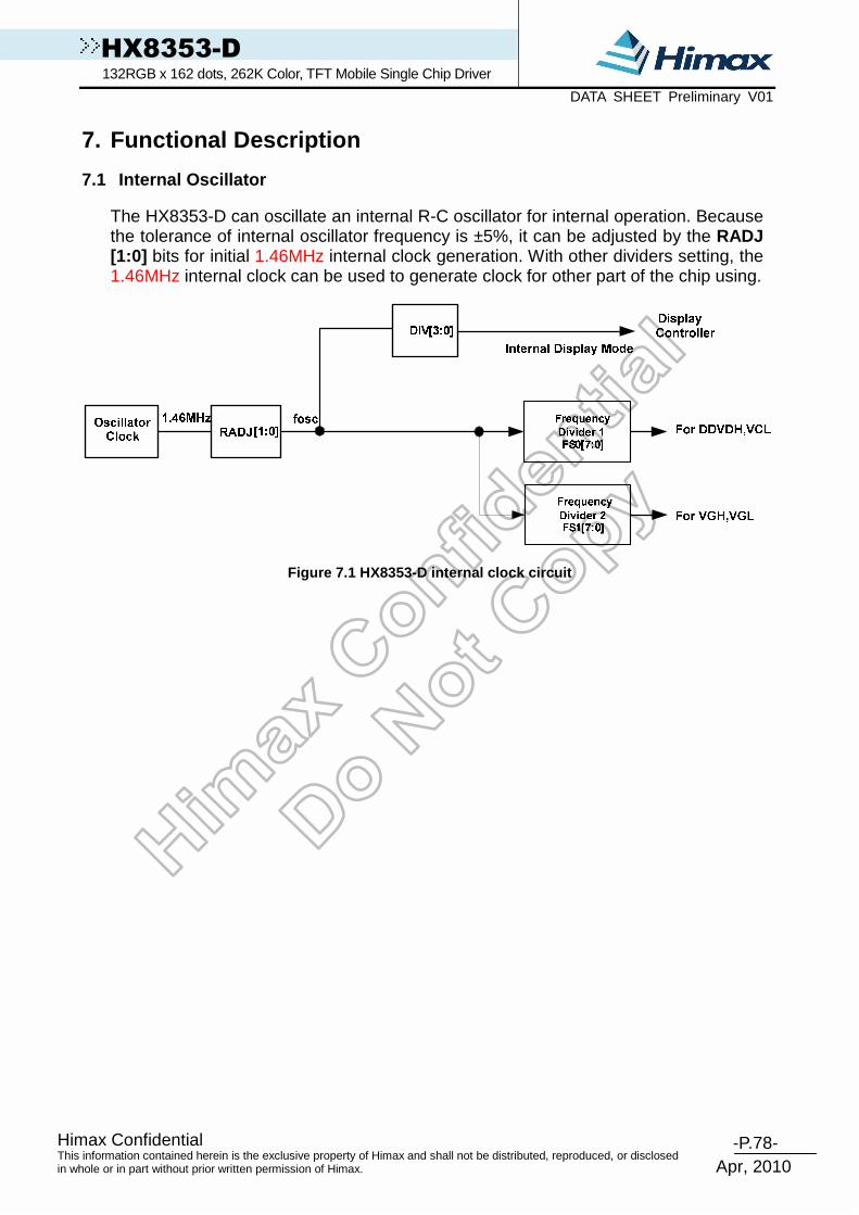
-P.78- Himax Confidential
Apr, 2010
This information contained herein is the exclusive property of Himax and shall not be distributed, reproduced, or disclosed in whole or in part without prior written permission of Himax.
HX8353-D 132RGB x 162 dots, 262K Color, TFT Mobile Single Chip Driver DATA SHEET Preliminary V01
7. Functional Description 7.1 Internal Oscillator
The HX8353-D can oscillate an internal R-C oscillator for internal operation. Because the tolerance of internal oscillator frequency is ±5%, it can be adjusted by the RADJ [1:0] bits for initial 1.46MHz internal clock generation. With other dividers setting, the 1.46MHz internal clock can be used to generate clock for other part of the chip using.
Figure 7.1 HX8353-D internal clock circuit
-P.79- Himax Confidential
Apr, 2010
This information contained herein is the exclusive property of Himax and shall not be distributed, reproduced, or disclosed in whole or in part without prior written permission of Himax.
HX8353-D 132RGB x 162 dots, 262K Color, TFT Mobile Single Chip Driver DATA SHEET Preliminary V01
7.2 Gamma characteristic correction function
The HX8353-D incorporates gamma adjustment function for the 262,144-color display (64 grayscale for each R, G, B color). Gamma adjustment operation is implemented by deciding the 8 grayscale levels firstly in gamma adjustment control registers to match the LCD panel. These registers are available for both polarities.

-P.80- Himax Confidential
Apr, 2010
This information contained herein is the exclusive property of Himax and shall not be distributed, reproduced, or disclosed in whole or in part without prior written permission of Himax.
HX8353-D 132RGB x 162 dots, 262K Color, TFT Mobile Single Chip Driver DATA SHEET Preliminary V01
Grayscale
Voltage
Generator
6-bit Grayscale
D/A Converter
Output Driver Output Driver Output Driver
6-bit Grayscale
D/ A Converter
6- bit Grayscale
D/ A Converter
R G B
LCD
V0
V1
V63
GraphicsRAM(GRAM)
6
32 31 30
42 41
2022 21CP23
PositivepolarityRegister
CPCP CP
02 01 00
12 11 10
22 21 20
32 31 30
42 41 40
52 51 50
40
MP MP MP
MP MP MP
MP MP MP
CP CP CP
CP CP CP
MP MP MP
MPMP MP
MP MP MP
NegativepolarityRegistre
02 01 00
12 11 10
01 00
1012 11ON
14
02
MN
MN
MN
MN
MN
MN
CN
CN
ON
ON
MN
MN
MN
MN
MN
MN
CN
CN
ON
ON
MN
MN
MN
MN
MN
MN
CN
CN
ON
ON
ON
ON
02 01 00
12 11 10
22 21 20
32 31 30
42 41 40
52 51 50
13
03
6 6
B3B2B1B0
G5G3G2G1G0
G4
B5B4
R5
R3R2R1R0
R4
CP33
CP43
CN03
02 01 00
12 11
01 00
1012 11OP14 OP13
0203 OP OP
OPOP OP
OPOP
10
CP CP CP
CP CP CP
CP03CP13
CN
CN
CN
CN
CN
CN
CN
CN
CN
22 21 20
32 31 30
42 41 40
CN
CN
23
03
CN33
CN43
Figure 7.2 Grayscale control
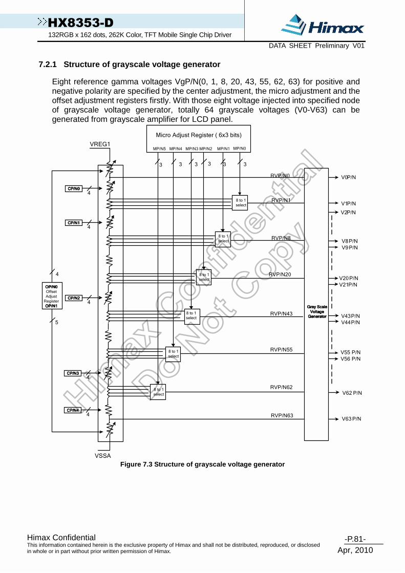
-P.81- Himax Confidential
Apr, 2010
This information contained herein is the exclusive property of Himax and shall not be distributed, reproduced, or disclosed in whole or in part without prior written permission of Himax.
HX8353-D 132RGB x 162 dots, 262K Color, TFT Mobile Single Chip Driver DATA SHEET Preliminary V01
7.2.1 Structure of grayscale voltage generator
Eight reference gamma voltages VgP/N(0, 1, 8, 20, 43, 55, 62, 63) for positive and negative polarity are specified by the center adjustment, the micro adjustment and the offset adjustment registers firstly. With those eight voltage injected into specified node of grayscale voltage generator, totally 64 grayscale voltages (V0-V63) can be generated from grayscale amplifier for LCD panel.
VSSA
VREG1
4
5
Micro Adjust Register ( 6x3 bits)
333333
MP/N5
V0P/N
V8P/N
V9P/N
V20P/N
V21P/N
V43P/NV44P/N
V55 P/N
V56 P/N
RVP/N0
V63P/N
V62 P/N
V1P/N
V2P/N
MP/N4 MP/N3 MP/N2 MP/N1 MP/N0
8 to 1
selectRVP/N1
RVP/N8
RVP/N20
RVP/N43
RVP/N55
RVP/N62
RVP/N63
OPOPOPOP////NNNN0000
OffsetAdjust
RegisterOPOPOPOP////NNNN1111 Gray Scale Gray Scale Gray Scale Gray Scale
Voltage Voltage Voltage Voltage GeneratorGeneratorGeneratorGenerator
4CPCPCPCP////NNNN0000
8 to 1
select
8 to 1 select
8 to 1 select
8 to 1
select
8 to 1 select
4CPCPCPCP////NNNN1111
4CPCPCPCP////NNNN2222
4CPCPCPCP////NNNN3333
4CPCPCPCP////NNNN4444
Figure 7.3 Structure of grayscale voltage generator

-P.82- Himax Confidential
Apr, 2010
This information contained herein is the exclusive property of Himax and shall not be distributed, reproduced, or disclosed in whole or in part without prior written permission of Himax.
HX8353-D 132RGB x 162 dots, 262K Color, TFT Mobile Single Chip Driver DATA SHEET Preliminary V01
7.2.2 Gamma-characteristics adjustment register
This HX8353-D has register groups for specifying a series grayscale voltage that meets the Gamma-characteristics for the LCD panel. These registers are divided into two groups, which correspond to the gradient, amplitude, and macro adjustment of the voltage for the grayscale characteristics. The polarity of each register can be specified independently. (R, G, and B are common.)
7.2.2.1 Offset adjustment registers 0/1 The offset adjustment variable registers are used to adjust the amplitude of the grayscale voltage. This function is implemented by controlling these variable resisters in the top and bottom of the gamma resister stream for reference gamma voltage generation. These registers are available for both positive and negative polarities
7.2.2.2 Gamma center adjustment registers
The gamma center adjustment registers are used to adjust the reference gamma voltage in the middle level of grayscale without changing the dynamic range. This function is implemented by controlling these variable resisters in center of the gamma resister stream for reference gamma voltage generation. These registers are available for both positive and negative polarities.
7.2.2.3 Gamma macro adjustment registers
The gamma macro adjustment registers can be used for fine adjustment of the reference gamma voltage. This function is implemented by controlling the 8-to-1 selectors (MP/N0~5), each of which has 8 inputs and generate one reference voltage output (RVP/N 0, 1, 8, 20, 44, 56, 63, 64). These registers are available for both positive and negative polarities.
Register Groups
Positive Polarity Description
CP/N0 3-0 Variable resistor (VRTP/N) for center adjustment CP/N1 3-0 Variable resistor (VRCP/N0)for center adjustment CP/N2 3-0 Variable resistor (VRMP/N) for center adjustment CP/N3 3-0 Variable resistor (VRCP/N1)for center adjustment
Center Adjustment
CP/N4 3-0 Variable resistor (VRBP/N)for center adjustment MP/N0 2-0 8-to-1 selector (reference voltage level of grayscale 1) MP/N1 2-0 8-to-1 selector (reference voltage level of grayscale 8) MP/N2 2-0 8-to-1 selector (reference voltage level of grayscale 20) MP/N3 2-0 8-to-1 selector (reference voltage level of grayscale 43) MP/N4 2-0 8-to-1 selector (reference voltage level of grayscale 55)
Macro Adjustment
MP/N5 2-0 8-to-1 selector (reference voltage level of grayscale 62) OP/N0 3-0 Variable resistor (VRP/N0)for offset adjustment Offset
Adjustment OP/N1 4-0 Variable resistor (VRP/N1)for offset adjustment Table 7.1 Gamma-adjustment registers

-P.83- Himax Confidential
Apr, 2010
This information contained herein is the exclusive property of Himax and shall not be distributed, reproduced, or disclosed in whole or in part without prior written permission of Himax.
HX8353-D 132RGB x 162 dots, 262K Color, TFT Mobile Single Chip Driver DATA SHEET Preliminary V01
7.2.3 Gamma resister stream and 8 to 1 selector
The block consists of two gamma resister streams, one is for positive polarity and the other is for negative polarity, each one includes eight gamma reference voltages (Vg(P/N)0, 1, 8, 20, 43, 55, 62, 63).
VREG1OPOPOPOP////NNNN1111
0000----93939393RRRR
VP/N0 VgP/N0
V0 P/N
VP/N1
VP/N2
VP/N3
VP/N4
VP/N5
VP/N6
VP/N7
VP/N10
VP/N11
VP/N12
VP/N13
VP/N14
VP/N15
VP/N16
VP/N18
VP/N19
VP/N20
VP/N21
VP/N22
VP/N23
VP/N24
VP/N26
VP/N27
VP/N28
VP/N29
VP/N30
VP/N31
VP/N32
VP/N34
VP/N35
VP/N36
VP/N37
VP/N38
VP/N39
VP/N40
VP/N42
VP/N43
VP/N44
VP/N45
VgP/N1
VgP/N2
VgP/N3
VgP/N4
VgP/N5
VgP/N6
VgP/N7
Buffer
Buffer
Buffer
Buffer
Buffer
Buffer
Center adjustment CP/N1
Center adjustment CP/N3
0 0 0 0----45454545RRRR OP OP OP OP////NNNN0000
VSSA
2 2 2 2RRRR****7777
0000----45454545RRRR
2R*7
2R*7
2R*7
20202020RRRR
2 2 2 2RRRR****7777
0-45R
V1 P/N
V2 P/N
V3 P/N
V4 P/N
V5 P/N
V6 P/N
V7 P/N
V8 P/N
V9 P/N
V10 P/N
V19 P/N
V20 P/N
V22 P/N
V21 P/N
V41 P/N
V42 P/N
V43 P/N
V44 P/N
V45 P/N
V54 P/N
V55 P/N
V56 P/N
V57 P/N
V58 P/N
V59 P/N
V60 P/N
V61 P/N
V62 P/N
V63 P/N
2 2 2 2RRRR****7777R1
R2
R3
R4
R5
R6
R7
R8
R9
R19
R20
R21
R41
R42
R43
R44
R53
R54
R55
R56
R57
R58
R59
R60
R61
20202020RRRR
0-30R
Center adjustment CP/N00000----60606060RRRR
0-60R Center adjustment CP/N4
Center adjustment CP/N2
CGM00 1 2 3
1R 3R 5R 2R
3.33R1.5R1R
1R
1R
1R
1R
1R
2R
1R
1R
1R
1R
1R
1R
1R
1R
1.5R
1.33R
1.17R
1R
1.83R
2.67R1.67R
0 1 2 3
1R
3R 5R 2R
3.33R1.5R
1R
1R
1R
1R
1R
1R
2R
1R
1R
1R
1R
1R
1R
1R
1R 1.5R
1.17R
1R
1.83R
2.67R
1.33R
1.67R
CGM1
VP/N8
VP/N9
VP/N17
VP/N33
VP/N41
KVP/N0
KVP/N1
KVP/N11
KVP/N10
KVP/N9
KVP/N8
KVP/N6
KVP/N5
KVP/N4
KVP/N2
KVP/N3
KVP/N7
KVP/N12
KVP/N13
KVP/N14
KVP/N15
KVP/N16
KVP/N17
KVP/N18
KVP/N19
KVP/N20
KVP/N21
KVP/N22
KVP/N23
KVP/N24
KVP/N25
KVP/N26
KVP/N27
KVP/N28
KVP/N29
KVP/N30
KVP/N31
KVP/N32
KVP/N33
KVP/N34
KVP/N35
KVP/N36
KVP/N37
KVP/N38
KVP/N39
KVP/N40
KVP/N41
KVP/N42
KVP/N43
KVP/N44
KVP/N45
KVP/N46
KVP/N47
KVP/N48
VRP/N1
VRP/N0
VRTP/N
VRCP/N0
VRMP/N
VRCP/N1
VRBP/NKVP/N49
Figure 7.4 Gamma resister stream and gamma referenc e voltage

-P.84- Himax Confidential
Apr, 2010
This information contained herein is the exclusive property of Himax and shall not be distributed, reproduced, or disclosed in whole or in part without prior written permission of Himax.
HX8353-D 132RGB x 162 dots, 262K Color, TFT Mobile Single Chip Driver DATA SHEET Preliminary V01
7.2.4 Variable resister
There are two types of variable resistors, one is for center adjustment and the other is for offset adjustment. The resistances are decided by setting values in the center adjustment, offset adjustment registers. Their relationship is shown as below.
Value in Register
OP/N0 3-0 Resistance
VRP/N0 Value in Register
OP/N1 4-0 Resistance
VRP/N1 0000 0R 00000 0R 0001 3R 00001 3R 0010 6R 00010 6R
• •
• •
1101 39R 11101 87R 1110 42R 11110 90R 1111 45R 11111 93R
Table 7.2 Offset adjustment
Value in Register CP/N0 3-0
Resistance VRTP/N
Value in Register CP/N4 3-0
Resistance VRBP/N
Value in Register CP/N2 3-0
Resistance VRMP/N0
0000 0R 0000 0R 0000 0R 0001 4R 0001 4R 0001 2R 0010 8R 0010 8R 0010 4R
• •
• •
• •
• •
• •
1100 1100 48R 1100 24R 1101 52R 1101 52R 1101 26R 1110 56R 1110 56R 1110 28R 1111 60R 1111 60R 1111 30R
Value in Register
CP/N3 3-0 Resistance VRCP/N1
Value in Register CP/N1 3-0
Resistance VRCP/N0
0000 0R 0000 0R 0001 3R 0001 3R 0010 6R 0010 6R
• •
• •
• •
• •
1100 36R 1100 36R 1101 39R 1101 39R 1110 42R 1110 42R 1111 45R 1111 45R
Table 7.3 Center adjustment
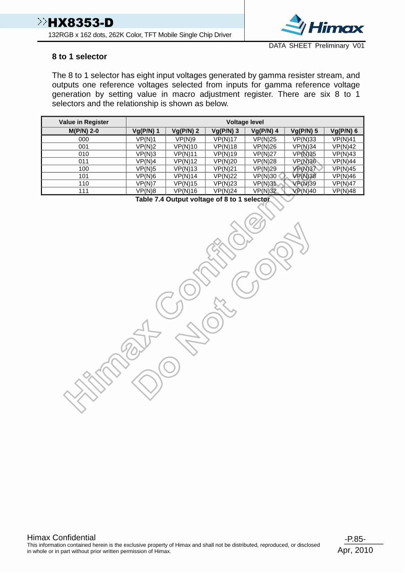
-P.85- Himax Confidential
Apr, 2010
This information contained herein is the exclusive property of Himax and shall not be distributed, reproduced, or disclosed in whole or in part without prior written permission of Himax.
HX8353-D 132RGB x 162 dots, 262K Color, TFT Mobile Single Chip Driver DATA SHEET Preliminary V01
8 to 1 selector
The 8 to 1 selector has eight input voltages generated by gamma resister stream, and outputs one reference voltages selected from inputs for gamma reference voltage generation by setting value in macro adjustment register. There are six 8 to 1 selectors and the relationship is shown as below.
Value in Register Voltage level
M(P/N) 2-0 Vg(P/N) 1 Vg(P/N) 2 Vg(P/N) 3 Vg(P/N) 4 Vg(P/N) 5 Vg(P/N) 6 000 VP(N)1 VP(N)9 VP(N)17 VP(N)25 VP(N)33 VP(N)41 001 VP(N)2 VP(N)10 VP(N)18 VP(N)26 VP(N)34 VP(N)42 010 VP(N)3 VP(N)11 VP(N)19 VP(N)27 VP(N)35 VP(N)43 011 VP(N)4 VP(N)12 VP(N)20 VP(N)28 VP(N)36 VP(N)44 100 VP(N)5 VP(N)13 VP(N)21 VP(N)29 VP(N)37 VP(N)45 101 VP(N)6 VP(N)14 VP(N)22 VP(N)30 VP(N)38 VP(N)46 110 VP(N)7 VP(N)15 VP(N)23 VP(N)31 VP(N)39 VP(N)47 111 VP(N)8 VP(N)16 VP(N)24 VP(N)32 VP(N)40 VP(N)48
Table 7.4 Output voltage of 8 to 1 selector

-P.86- Himax Confidential
Apr, 2010
This information contained herein is the exclusive property of Himax and shall not be distributed, reproduced, or disclosed in whole or in part without prior written permission of Himax.
HX8353-D 132RGB x 162 dots, 262K Color, TFT Mobile Single Chip Driver DATA SHEET Preliminary V01
The grayscale levels are determined by the following formulas. Reference
Voltage Formula
VgP/N0 - VREG1-VD*VRP/N1 /sumRP/N MP/N0 2-0=000 VREG1 –VD((VRP/N1+VRTP/N) /sumRP/N MP/N0 2-0=001 VREG1 –VD((VRP/N1+ VRTP/N +2R) /sumRP/N MP/N0 2-0=010 VREG1 –VD((VRP/N1+ VRTP/N +4R) /sumRP/N MP/N0 2-0=011 VREG1 –VD((VRP/N1+ VRTP/N +6R) /sumRP/N MP/N0 2-0=100 VREG1 –VD((VRP/N1+ VRTP/N +8R) /sumRP/N MP/N0 2-0=101 VREG1 –VD((VRP/N1+ VRTP/N +10R) /sumRP/N MP/N0 2-0=110 VREG1 –VD((VRP/N1+ VRTP/N +12R) /sumRP/N
VgP1/VgN7
MP/N0 2-0=111 VREG1 –VD((VRP/N1+ VRTP/N +14R) /sumRP/N MP/N1 2-0=000 VREG1 –VD((VRP/N1+ VRTP/N +14R+VRCP/N0) /sumRP/N MP/N1 2-0=001 VREG1 –VD((VRP/N1+ VRTP/N +16R+VRCP/N0) /sumRP/N MP/N1 2-0=010 VREG1 –VD((VRP/N1+ VRTP/N +18R+VRCP/N0) /sumRP/N MP/N1 2-0=011 VREG1 –VD((VRP/N1+ VRTP/N +20R+VRCP/N0) /sumRP/N MP/N1 2-0=100 VREG1 –VD((VRP/N1+ VRTP/N +22R+VRCP/N0) /sumRP/N MP/N1 2-0=101 VREG1 –VD((VRP/N1+ VRTP/N +24R+VRCP/N0) /sumRP/N MP/N1 2-0=110 VREG1 –VD((VRP/N1+ VRTP/N +26R+VRCP/N0) /sumRP/N
VgP2/VgN2
MP/N1 2-0=111 VREG1 –VD((VRP/N1+ VRTP/N +28R+VRCP/N0) /sumRP/N MP/N2 2-0=000 VREG1 –VD((VRP/N1+ VRTP/N+48R+VRCP/N0) /sumRP/N MP/N2 2-0=001 VREG1 –VD((VRP/N1+ VRTP/N+50R+VRCP/N0) /sumRP/N MP/N2 2-0=010 VREG1 –VD((VRP/N1+ VRTP/N+52R+VRCP/N0) /sumRP/N MP/N2 2-0=011 VREG1 –VD((VRP/N1+ VRTP/N+54R+VRCP/N0) /sumRP/N MP/N2 2-0=100 VREG1 –VD((VRP/N1+ VRTP/N+56R+VRCP/N0) /sumRP/N MP/N2 2-0=101 VREG1 –VD((VRP/N1+ VRTP/N+58R+VRCP/N0) /sumRP/N MP/N2 2-0=110 VREG1 –VD((VRP/N1+ VRTP/N+60R+VRCP/N0) /sumRP/N
VgP3/VgN3
MP/N2 2-0=111 VREG1 –VD((VRP/N1+ VRTP/N+62R+VRCP/N0) /sumRP/N MP/N3 2-0=000 VREG1 –VD((VRP/N1+ VRTP/N+ VRMP/N +62R+VRCP/N0) /sumRP/N MP/N3 2-0=001 VREG1 –VD((VRP/N1+ VRTP/N+ VRMP/N +64R+VRCP/N0) /sumRP/N MP/N3 2-0=010 VREG1 –VD((VRP/N1+ VRTP/N+ VRMP/N +66R+VRCP/N0) /sumRP/N MP/N3 2-0=011 VREG1 –VD((VRP/N1+ VRTP/N+ VRMP/N +68R+VRCP/N0) /sumRP/N MP/N3 2-0=100 VREG1 –VD((VRP/N1+ VRTP/N+ VRMP/N +70R+VRCP/N0) /sumRP/N MP/N3 2-0=101 VREG1 –VD((VRP/N1+ VRTP/N+ VRMP/N +72R+VRCP/N0) /sumRP/N MP/N3 2-0=110 VREG1 –VD((VRP/N1+ VRTP/N+ VRMP/N +74R+VRCP/N0) /sumRP/N
VgP4/VgN4
MP/N3 2-0=111 VREG1 –VD((VRP/N1+ VRTP/N+ VRMP/N +76R+VRCP/N0) /sumRP/N MP/N4 2-0=000 VREG1 –VD((VRP/N1+ VRTP/N+ VRMP/N +96R+VRCP/N0) /sumRP/N MP/N4 2-0=001 VREG1 –VD((VRP/N1+ VRTP/N+ VRMP/N +98R+VRCP/N0) /sumRP/N MP/N4 2-0=010 VREG1 –VD((VRP/N1+ VRTP/N+ VRMP/N +100R+VRCP/N0) /sumRP/N MP/N4 2-0=011 VREG1 –VD((VRP/N1+ VRTP/N+ VRMP/N +102R+VRCP/N0) /sumRP/N MP/N4 2-0=100 VREG1 –VD((VRP/N1+ VRTP/N+ VRMP/N +104R+VRCP/N0) /sumRP/N MP/N4 2-0=101 VREG1 –VD((VRP/N1+ VRTP/N+ VRMP/N +106R+VRCP/N0) /sumRP/N MP/N4 2-0=110 VREG1 –VD((VRP/N1+ VRTP/N+ VRMP/N +108R+VRCP/N0) /sumRP/N
VgP5/VgN5
MP/N4 2-0=111 VREG1 –VD((VRP/N1+ VRTP/N+ VRMP/N +110R+VRCP/N0) /sumRP/N MP/N5 2-0=000 VREG1 –VD((VRP/N1+ VRTP/N+ VRMP/N+110R+VRCP/N0 +VRCP/N1) /sumRP/N MP/N5 2-0=001 VREG1 –VD((VRP/N1+ VRTP/N+ VRMP/N +112R+VRCP/N0+VRCP/N1) /sumRP/N MP/N5 2-0=010 VREG1 –VD((VRP/N1+ VRTP/N+ VRMP/N +114R+VRCP/N0+VRCP/N1) /sumRP/N MP/N5 2-0=011 VREG1 –VD((VRP/N1+ VRTP/N+ VRMP/N +116R+VRCP/N0+VRCP/N1) /sumRP/N MP/N5 2-0=100 VREG1 –VD((VRP/N1+ VRTP/N+ VRMP/N +118R+VRCP/N0+VRCP/N1) /sumRP/N MP/N5 2-0=101 VREG1 –VD((VRP/N1+ VRTP/N+ VRMP/N +120R+VRCP/N0+VRCP/N1) /sumRP/N MP/N5 2-0=110 VREG1 –VD((VRP/N1+ VRTP/N+ VRMP/N +122R+VRCP/N0+VRCP/N1) /sumRP/N
VgP6/VgN6
MP/N5 2-0=111 VREG1 –VD((VRP/N1+ VRTP/N+ VRMP/N +124R+VRCP/N0+VRCP/N1) /sumRP/N
VgP7/VgN7 - VREG1 –VD((VRP/N1+ VRBP/N+ VRTP/N+ VRMP/N +104R+VRCP/N0+VRCP/N1) /sumRP/N
SumRP=124R+VRP0+ VRP1+ VRTP+ VRCP0+VRMP+VRCP1+VRBP SumRN=124R+ VRN0+ VRN1+ VRTN+ VRCN0+VRMN+VRCN1+VRBN VD=(VREG1–VSSA)
Table 7.5 Voltage calculation formula

-P.87- Himax Confidential
Apr, 2010
This information contained herein is the exclusive property of Himax and shall not be distributed, reproduced, or disclosed in whole or in part without prior written permission of Himax.
HX8353-D 132RGB x 162 dots, 262K Color, TFT Mobile Single Chip Driver DATA SHEET Preliminary V01
Grayscale
Voltage Formula Grayscale Voltage Formula
V0P/V63N VgP/N0 V32P/V31N VgP/N4+(VgP/N3-VgP/N4)*(11/23) V1P/V62N VgP/N1 V33P/V30N VgP/N4+(VgP/N3-VgP/N4)*(10/23) V2P/V61N VgP/N2+(VgP/N1-VgP/N2)*CT1 V34P/V29N VgP/N4+(VgP/N3-VgP/N4)*(9/23) V3P/V60N VgP/N2+(VgP/N1-VgP/N2)*CT2 V35P/V28N VgP/N4+(VgP/N3-VgP/N4)*(8/23) V4P/V59N VgP/N2+(VgP/N1-VgP/N2)*CT3 V36P/V27N VgP/N4+(VgP/N3-VgP/N4)*(7/23) V5P/V58N VgP/N2+(VgP/N1-VgP/N2)*CT4 V37P/V26N VgP/N4+(VgP/N3-VgP/N4)*(6/23) V6P/V57N VgP/N2+(VgP/N1-VgP/N2)*CT5 V38P/V25N VgP/N4+(VgP/N3-VgP/N4)*(5/23) V7P/V56N VgP/N2+(VgP/N1-VgP/N2)*CT6 V39P/V24N VgP/N4+(VgP/N3-VgP/N4)*(4/23) V8P/V55N VgP/N2 V40P/V23N VgP/N4+(VgP/N3-VgP/N4)*(3/23) V9P/V54N VgP/N3+(VgP/N2-VgP/N3)*(22/24) V41P/V22N VgP/N4+(VgP/N3-VgP/N4)*(2/23)
V10P/V53N VgP/N3+(VgP/N2-VgP/N3)*(20/24) V42P/V21N VgP/N4+(VgP/N3-VgP/N4)*(1/23) V11P/V52N VgP/N3+(VgP/N2-VgP/N3)*(18/24) V43P/V20N VgP/N4 V12P/V51N VgP/N3+(VgP/N2-VgP/N3)*(16/24) V44P/V19N VgP/N5+(VgP/N4-VgP/N5)*(22/24) V13P/V50N VgP/N3+(VgP/N2-VgP/N3)*(14/24) V45P/V18N VgP/N5+(VgP/N4-VgP/N5)*(20/24) V14P/V49N VgP/N3+(VgP/N2-VgP/N3)*(12/24) V46P/V17N VgP/N5+(VgP/N4-VgP/N5)*(18/24) V15P/V48N VgP/N3+(VgP/N2-VgP/N3)*(10/24) V47P/V16N VgP/N5+(VgP/N4-VgP/N5)*(16/24) V16P/V47N VgP/N3+(VgP/N2-VgP/N3)*(8/24) V48P/V15N VgP/N5+(VgP/N4-VgP/N5)*(14/24) V17P/V46N VgP/N3+(VgP/N2-VgP/N3)*(6/24) V49P/V14N VgP/N5+(VgP/N4-VgP/N5)*(12/24) V18P/V45N VgP/N3+(VgP/N2-VgP/N3)*(4/24) V50P/V13N VgP/N5+(VgP/N4-VgP/N5)*(10/24) V19P/V44N VgP/N3+(VgP/N2-VgP/N3)*(2/24) V51P/V12N VgP/N5+(VgP/N4-VgP/N5)*(8/24) V20P/V43N VgP/N3 V52P/V11N VgP/N5+(VgP/N4-VgP/N5)*(6/24) V21P/V42N VgP/N4+(VgP/N3-VgP/N4)*(22/23) V53P/V10N VgP/N5+(VgP/N4-VgP/N5)*(4/24) V22P/V41N VgP/N4+(VgP/N3-VgP/N4)*(21/23) V54P/V9N VgP/N5+(VgP/N4-VgP/N5)*(2/24) V23P/V40N VgP/N4+(VgP/N3-VgP/N4)*(20/23) V55P/V8N VgP/N5 V24P/V39N VgP/N4+(VgP/N3-VgP/N4)*(19/23) V56P/V7N VgP/N6+(VgP/N5-VgP/N6)*CB1 V25P/V38N VgP/N4+(VgP/N3-VgP/N4)*(18/23) V57P/V6N VgP/N6+(VgP/N5-VgP/N6)*CB2 V26P/V37N VgP/N4+(VgP/N3-VgP/N4)*(17/23) V58P/V5N VgP/N6+(VgP/N5-VgP/N6)*CB3 V27P/V36N VgP/N4+(VgP/N3-VgP/N4)*(16/23) V59P/V4N VgP/N6+(VgP/N5-VgP/N6)*CB4 V28P/V35N VgP/N4+(VgP/N3-VgP/N4)*(15/23) V60P/V3N VgP/N6+(VgP/N5-VgP/N6)*CB5 V29P/V34N VgP/N4+(VgP/N3-VgP/N4)*(14/23) V61P/V2N VgP/N6+(VgP/N5-VgP/N6)*CB6 V30P/V33N VgP/N4+(VgP/N3-VgP/N4)*(13/23) V62P/V1N VgP/N6 V31P/V32N VgP/N4+(VgP/N3-VgP/N4)*(12/23) V63P/V0N VgP/N7
Table 7.6 Voltage calculation formula of grayscale voltage
CGM0[1:0] “00” “01” “10” “11” CGM1[1:0] “00” “01” “10” “11” CT1 6/7 7.5/10.5 10/15 8.5/10.5 CB1 6/7 9.5/10.5 14/15 9.5/10.5 CT2 5/7 6/10.5 6.67/15 6.67/10.5 CB2 5/7 8.5/10.5 13/15 8.33/10.5 CT3 4/7 4/10.5 4/15 5.0/10.5 CB3 4/7 7.5/10.5 12/15 7.0/10.5 CT4 3/7 3/10.5 3/15 3.5/10.5 CB4 3/7 6.5/10.5 11/15 5.5/10.5 CT5 2/7 2/10.5 2/15 2.17/10.5 CB5 2/7 4.5/10.5 8.33/15 3.83/10.5 CT6 1/7 1/10.5 1/15 1/10.5
CB6 1/7 3.0/10.5 5/15 2.0/10.5 Note: Negative gamma don’t have CGM0/CGM1 setting, the ratio V2~V7 and V56~V61 is automatically mapping from
positive side. Table 7.7 Voltage calculation formula of grayscale voltage V2~V7 and V56~V61

-P.88- Himax Confidential
Apr, 2010
This information contained herein is the exclusive property of Himax and shall not be distributed, reproduced, or disclosed in whole or in part without prior written permission of Himax.
HX8353-D 132RGB x 162 dots, 262K Color, TFT Mobile Single Chip Driver DATA SHEET Preliminary V01
Relationship between GRAM Data and Output Level (“N ormally White Panel”, GRAM data=0)
Figure 7.5 Relationship between source output and V COM
Negative polarity
Positive polarity
000000 111111RAM Data
(Same characteristic for each RGB)
V63
V0
Output Level
Figure 7.6 Relationship between GRAM data and outpu t level (normal white panel REV_Panel=“0”)

-P.89- Himax Confidential
Apr, 2010
This information contained herein is the exclusive property of Himax and shall not be distributed, reproduced, or disclosed in whole or in part without prior written permission of Himax.
HX8353-D 132RGB x 162 dots, 262K Color, TFT Mobile Single Chip Driver DATA SHEET Preliminary V01
Four-characteristic gamma curve selection There are four kind of Gamma Curve is selected by GAMSET command. The parameter GC[7:0] is stored in internal register and used to select one set of gamma correction register. GC_SEL=“L”:
Figure 7.7 Gamma curve according to GC0 to GC3 bit (GC_SEL=”L”)
GC_SEL=“H”:
Figure 7.8 Gamma curve according to GC0 to GC3 bit (GC_SEL=”H”)

-P.90- Himax Confidential
Apr, 2010
This information contained herein is the exclusive property of Himax and shall not be distributed, reproduced, or disclosed in whole or in part without prior written permission of Himax.
HX8353-D 132RGB x 162 dots, 262K Color, TFT Mobile Single Chip Driver DATA SHEET Preliminary V01
7.3 Tearing effect output line
The Tearing Effect output line supplies to the MPU a Panel synchronization signal. This signal can be enabled or disabled by the Tearing Effect Line off & on commands. The mode of the Tearing Effect signal is defined by the parameter of the Tearing Effect Line On command. The signal can be used by the MPU to synchronize Frame Memory Writing when displaying video images.
7.3.1 Tearing effect line modes
Mode 1: The Tearing Effect Output signal consists of V-Blanking Information only:
tVdh= The LCD display is not updated from the Frame Memory tvdl = The LCD display is updated from the Frame Memory (except Invisible Line – see below)
Figure 7.9 TE mode 1 output
Mode 2: The Tearing Effect Output signal consists of V-Blanking and H-Blanking
Information, there is one V-sync and N H-sync pulses per field on different resolution.
128RGBx160: N=160
132RGBx162: N=162
96x68: N=68

-P.91- Himax Confidential
Apr, 2010
This information contained herein is the exclusive property of Himax and shall not be distributed, reproduced, or disclosed in whole or in part without prior written permission of Himax.
HX8353-D 132RGB x 162 dots, 262K Color, TFT Mobile Single Chip Driver DATA SHEET Preliminary V01
96x64: N=64
Figure 7.10 TE mode 2 output thdh= The LCD display is not updated from the Frame Memory thdl= The LCD display is updated from the Frame Memory (except Invisible Line – see above.)
Note: During Sleep In Mode, the Tearing Output Pin is active Low.
Figure 7.11 TE output waveform

-P.92- Himax Confidential
Apr, 2010
This information contained herein is the exclusive property of Himax and shall not be distributed, reproduced, or disclosed in whole or in part without prior written permission of Himax.
HX8353-D 132RGB x 162 dots, 262K Color, TFT Mobile Single Chip Driver DATA SHEET Preliminary V01
7.3.2 Tearing effect line timing
The Tearing Effect signal is described below.
Figure 7.12 Waveform of tearing effect signal
Idle Mode Off (Frame Rate=60Hz)
Symbol Parameter Min. Max. Unit Description tvdl Vertical Timing Low Duration TBD - ms - tvdh Vertical Timing High Duration 1000 - µs - thdl Horizontal Timing Low Duration TBD - µs - thdh Horizontal Timing High Duration TBD 500 µs -
Table 7.8 AC characteristics of tearing effect sign al The signal’s rise and fall times (tf, tr) are stipulated to be equal to or less than 15ns.
Figure 7.13 Timing of tearing effect signal
The Tearing Effect Output Line is fed back to the MPU and should be used as shown below to avoid Tearing Effect:

-P.93- Himax Confidential
Apr, 2010
This information contained herein is the exclusive property of Himax and shall not be distributed, reproduced, or disclosed in whole or in part without prior written permission of Himax.
HX8353-D 132RGB x 162 dots, 262K Color, TFT Mobile Single Chip Driver DATA SHEET Preliminary V01
7.3.3 Example 1: MPU write is faster than panel rea d
Figure 7.14 Timing of MPU write is faster than pane l read
Data write to frame memory is now synchronized to the panel scan. It should be written during the vertical sync pulse of the tearing effect output line. This ensures that data is always written ahead of the panel scan and each panel frame refresh has a complete new image:
Figure 7.15 Display of MPU write is faster than pan el read
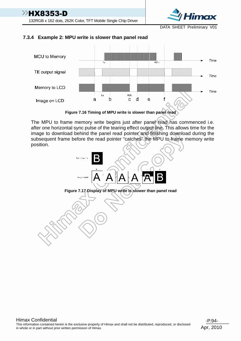
-P.94- Himax Confidential
Apr, 2010
This information contained herein is the exclusive property of Himax and shall not be distributed, reproduced, or disclosed in whole or in part without prior written permission of Himax.
HX8353-D 132RGB x 162 dots, 262K Color, TFT Mobile Single Chip Driver DATA SHEET Preliminary V01
7.3.4 Example 2: MPU write is slower than panel rea d
Figure 7.16 Timing of MPU write is slower than pane l read
The MPU to frame memory write begins just after panel read has commenced i.e. after one horizontal sync pulse of the tearing effect output line. This allows time for the image to download behind the panel read pointer and finishing download during the subsequent frame before the read pointer “catches” the MPU to frame memory write position.
Figure 7.17 Display of MPU write is slower than pan el read

-P.95- Himax Confidential
Apr, 2010
This information contained herein is the exclusive property of Himax and shall not be distributed, reproduced, or disclosed in whole or in part without prior written permission of Himax.
HX8353-D 132RGB x 162 dots, 262K Color, TFT Mobile Single Chip Driver DATA SHEET Preliminary V01
7.4 Scan Mode Setting
HX8353-D can set internal register GS_PANEL bit to determine the pin assignment of gate. The
GS_PANEL setting allows changing the shift direction of gate outputs by connecting LCD panel
with the HX8353-D.
G2 to G162
G1 to G161
G162 to G2
G161 to G1
Figure 7.18 Gate Scan Mode

-P.96- Himax Confidential
Apr, 2010
This information contained herein is the exclusive property of Himax and shall not be distributed, reproduced, or disclosed in whole or in part without prior written permission of Himax.
HX8353-D 132RGB x 162 dots, 262K Color, TFT Mobile Single Chip Driver DATA SHEET Preliminary V01
7.5 LCD power generation circuit 7.5.1 Power supply circuit
The power circuit of HX8353-D is used to generate supply voltages for LCD panel driving.
Step up
Circuit 1
C11A
C11B
DDVDH
Reference
Voltage
GenerationCircuit
C12A
C12B
VREG1
Step up
Circuit 2
C21A
C21B
C22A
C22B
VGH
VGL
VDDD
Reference
VoltageGenerationCircuit
VCI
VSSA
VSSD
IOVCC
VCL
Figure 7.19 Block diagram of HX8353-D power circuit

-P.97- Himax Confidential
Apr, 2010
This information contained herein is the exclusive property of Himax and shall not be distributed, reproduced, or disclosed in whole or in part without prior written permission of Himax.
HX8353-D 132RGB x 162 dots, 262K Color, TFT Mobile Single Chip Driver DATA SHEET Preliminary V01
Specification of Connected Passive Component
Capacitor Recommended voltage Capacity
C1 (DDVDH) 6.3V 1 µF (B characteristics) C2 (C11) 6.3V 1 µF (B characteristics) C3 (VGL) 16V 1 µF (B characteristics)
Table 7.9 The adoptability of Capacitor
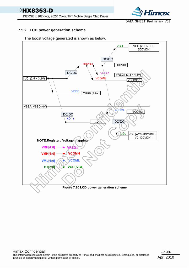
-P.98- Himax Confidential
Apr, 2010
This information contained herein is the exclusive property of Himax and shall not be distributed, reproduced, or disclosed in whole or in part without prior written permission of Himax.
HX8353-D 132RGB x 162 dots, 262K Color, TFT Mobile Single Chip Driver DATA SHEET Preliminary V01
7.5.2 LCD power generation scheme
The boost voltage generated is shown as below.
VSSA, VSSD (0V)
VREG1 (3.3 ~ 4.8V)
VCOMH
VGH (2DDVDH ~
3DDVDH)
VCOML
VCL
VGH
x (-1)
VCI (2.5 ~ 3.3V).
DDVDHDDVDH
VDDD (1.6V)
VGL (-VCI-2DDVDH ~
-VCI-DDVDH)
DC/DC
DC/DC
DC/DC
DC/DC
VCOMLVML[6:0]
VGH, VGLBT[2:0]
VGL
VCOML
VCOMH
VDDD
VREG1
VCOMHVMH[6:0]
VREG1VRH[4:0]
NOTE:Register / Voltage mapping
Figure 7.20 LCD power generation scheme

-P.99- Himax Confidential
Apr, 2010
This information contained herein is the exclusive property of Himax and shall not be distributed, reproduced, or disclosed in whole or in part without prior written permission of Himax.
HX8353-D 132RGB x 162 dots, 262K Color, TFT Mobile Single Chip Driver DATA SHEET Preliminary V01
7.6 Power function
7.6.1 Power on/off sequence
Power source IOVCC, VCI can be applied and powered down in any order. IOVCC, VCI can be powered down in any order. During power off, if LCD is in the Sleep Out mode, IOVCC, VCI must be powered down minimum 120msec after NRESET has been released. During power off, if LCD is in the Sleep In mode, IOVCC, VCI can be powered down minimum 0msec after NRESET has been released. NCS can be applied at any timing or can be permanently grounded. NRESET has priority over NCS. Note: (1) There will be no damage to the display module if the power sequences are not met.
(2) There will be no abnormal visible effects on the display panel during the Power On/Off Sequences. (3) There will be no abnormal visible effects on the display between end of Power on Sequence and before
receiving Sleep Out command. Also between receiving Sleep In command and Power Off Sequence. (4) If NRESET line is not held stable by host during Power on Sequence as defined in Sections 7.5.1.1 and
7.5.1.2, then it will be necessary to apply a Hardware Reset (NRESET) after Host Power on Sequence to ensure correct operation. Otherwise correct function is not guaranteed.
If NRESET line is not held stable by host during Power on Sequence as defined in Sections 7.5.1.1 and 7.5.1.2, then it will be necessary to apply a Hardware Reset (NRESET) after Host Power on Sequence is complete to ensure correct operation, otherwise correct functionality is not guaranteed. The power on/off sequence is illustrated as below.
7.6.1.1 Case 1 – NRESET line is held high or unstab le by host at power on
If NRESET line is held high or unstable by the host during Power On, then a Hardware Reset must be applied after both IOVCC, VCI have been applied, otherwise correct functionality is not guaranteed. There is no timing restriction upon this hardware reset.

-P.100- Himax Confidential
Apr, 2010
This information contained herein is the exclusive property of Himax and shall not be distributed, reproduced, or disclosed in whole or in part without prior written permission of Himax.
HX8353-D 132RGB x 162 dots, 262K Color, TFT Mobile Single Chip Driver DATA SHEET Preliminary V01
IOVCC
VCI
NCS
NRESET
NRESET
tRPW= +/- no limit tFPW= +/- no limit
tRPWNCS= +/- no limit tFPWNCS= +/- no limit
H or L
tRPWNRES= + no limit
tRPWNRES= + no limit
tFPWNRES1= min 120ms
tFPWNRES2= min 0ns
(Power down in
sleep out mode)
( Power down insleep in mode)
tFPWNRES1 is applied to NRESET falling in the Sleep Out ModetFPWNRES2 is applied to NRESET falling in the Sleep In Mode
Time when the latter signal rises up to 90% of its typical
value
.
Time when the former signal falls down to 90% of its
Typical value
NoteNoteNoteNote: : : : Unless otherwise specified, timings herein show cross point at 50% of signal/power level.
Figure 7.21 Case 1 – NRESET line is held high or un stable by host at power on

-P.101- Himax Confidential
Apr, 2010
This information contained herein is the exclusive property of Himax and shall not be distributed, reproduced, or disclosed in whole or in part without prior written permission of Himax.
HX8353-D 132RGB x 162 dots, 262K Color, TFT Mobile Single Chip Driver DATA SHEET Preliminary V01
7.6.1.2 Case 2 – NRESET line is held low by host at power on
If NRESET line is held Low (and stable) by the host during Power On, then the NRESET must be held low for minimum 10µsec after VCI have been applied.
IOVCC
NCS
NRESET
NRESET
tRPW= +/- no limit tFPW= +/- no limit
tRPWNCS = +/- no limit
H or L
tRPWNRES= min 10us
tRPWNRES= min 10us
tFPWNRES1= min 120ms
tFPWNRES2 = min 0ns
tFPWNRES1 is applied to NREST falling in the Sleep Out ModetFPWNRES2 is applied to NREST falling in the Sleep In Mode
( Power down in Sleep Out mode )
(Power down in Sleep In mode )
.
tRPWNCS = +/- no limit
VCI
Time when the latter signal rises up to 90% of its typical value
Time when the former signal falls down to 90% of its Typical
value
NoteNoteNoteNote:::: Unless otherwise specified, timings herein show cross point at 50% of signal/power level. Figure 7.22 NRESET Line is Held Low by Host at Powe r On

-P.102- Himax Confidential
Apr, 2010
This information contained herein is the exclusive property of Himax and shall not be distributed, reproduced, or disclosed in whole or in part without prior written permission of Himax.
HX8353-D 132RGB x 162 dots, 262K Color, TFT Mobile Single Chip Driver DATA SHEET Preliminary V01
7.6.2 Power levels definition
7.6.2.1 General definition for power levels on syst em interface
Figure 7.23 Power flow chart for different power mo des

-P.103- Himax Confidential
Apr, 2010
This information contained herein is the exclusive property of Himax and shall not be distributed, reproduced, or disclosed in whole or in part without prior written permission of Himax.
HX8353-D 132RGB x 162 dots, 262K Color, TFT Mobile Single Chip Driver DATA SHEET Preliminary V01
7.6.3 Deep standby mode set up flow
Wait >20ms
Set deep
standby
Display on
Display off flow
SLEEP IN
Set deep standby
(DP_STB_S = "1", RB1h=01h)
Set deep standby
(DP_STB = "1",RB1h=03h)
Set deep standby (DP_STB = "0",RB1h=01h)
Set deep standby (DP_STB_S = "0",RB1h=00h)
SLEEP OUT
SETEXTC
(RB9h=FFh,83h,53h)
Release
deep standby
Figure 7.24 Deep standby mode setting flow
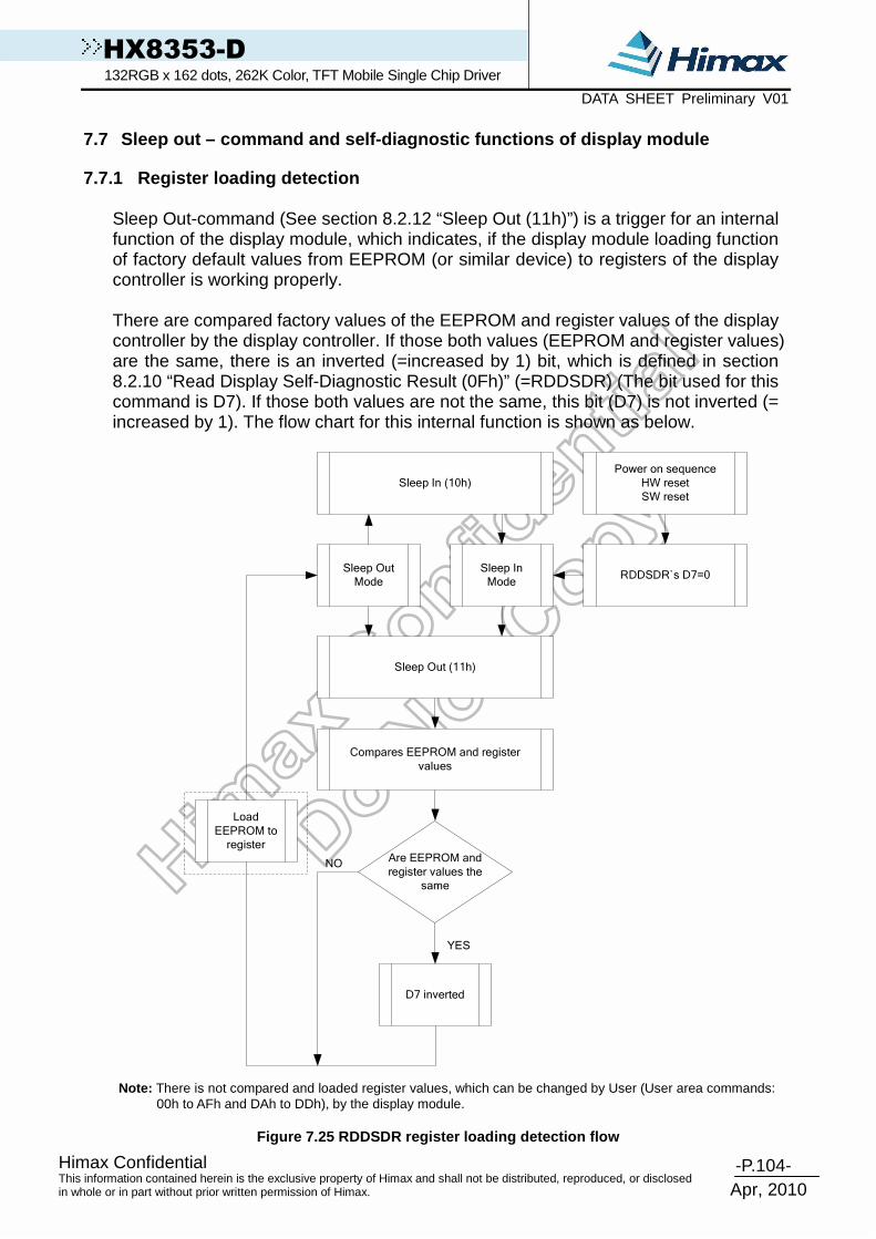
-P.104- Himax Confidential
Apr, 2010
This information contained herein is the exclusive property of Himax and shall not be distributed, reproduced, or disclosed in whole or in part without prior written permission of Himax.
HX8353-D 132RGB x 162 dots, 262K Color, TFT Mobile Single Chip Driver DATA SHEET Preliminary V01
7.7 Sleep out – command and self-diagnostic functio ns of display module
7.7.1 Register loading detection
Sleep Out-command (See section 8.2.12 “Sleep Out (11h)”) is a trigger for an internal function of the display module, which indicates, if the display module loading function of factory default values from EEPROM (or similar device) to registers of the display controller is working properly. There are compared factory values of the EEPROM and register values of the display controller by the display controller. If those both values (EEPROM and register values) are the same, there is an inverted (=increased by 1) bit, which is defined in section 8.2.10 “Read Display Self-Diagnostic Result (0Fh)” (=RDDSDR) (The bit used for this command is D7). If those both values are not the same, this bit (D7) is not inverted (= increased by 1). The flow chart for this internal function is shown as below.
Sleep In (10h)
Sleep Out
Mode
Sleep In
Mode
Sleep Out (11h)
Compares EEPROM and register
values
Are EEPROM and
register values the
same
D7 inverted
RDDSDR`s D7=0
Power on sequence
HW reset
SW reset
YES
NO
Load
EEPROM to
register
Note: There is not compared and loaded register values, which can be changed by User (User area commands:
00h to AFh and DAh to DDh), by the display module.
Figure 7.25 RDDSDR register loading detection flow
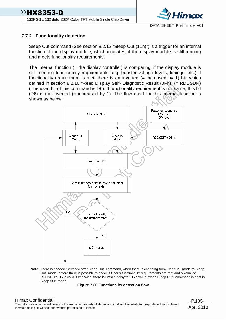
-P.105- Himax Confidential
Apr, 2010
This information contained herein is the exclusive property of Himax and shall not be distributed, reproduced, or disclosed in whole or in part without prior written permission of Himax.
HX8353-D 132RGB x 162 dots, 262K Color, TFT Mobile Single Chip Driver DATA SHEET Preliminary V01
7.7.2 Functionality detection
Sleep Out-command (See section 8.2.12 “Sleep Out (11h)”) is a trigger for an internal function of the display module, which indicates, if the display module is still running and meets functionality requirements. The internal function (= the display controller) is comparing, if the display module is still meeting functionality requirements (e.g. booster voltage levels, timings, etc.) If functionality requirement is met, there is an inverted (= increased by 1) bit, which defined in section 8.2.10 “Read Display Self- Diagnostic Result (0Fh)” (= RDDSDR) (The used bit of this command is D6). If functionality requirement is not same, this bit (D6) is not inverted (= increased by 1). The flow chart for this internal function is shown as below.
Note: There is needed 120msec after Sleep Out -command, when there is changing from Sleep In –mode to Sleep
Out -mode, before there is possible to check if User’s functionality requirements are met and a value of RDDSDR’s D6 is valid. Otherwise, there is 5msec delay for D6’s value, when Sleep Out –command is sent in Sleep Out -mode.
Figure 7.26 Functionality detection flow

-P.106- Himax Confidential
Apr, 2010
This information contained herein is the exclusive property of Himax and shall not be distributed, reproduced, or disclosed in whole or in part without prior written permission of Himax.
HX8353-D 132RGB x 162 dots, 262K Color, TFT Mobile Single Chip Driver DATA SHEET Preliminary V01
7.8 Input / output pin state 7.8.1 Output pins
Output or Bi-directional pins After Power On After Hardware
Reset After Software Reset
TE Low Low Low DB17 to DB0
(Output driver) High-Z (Inactive) High-Z (Inactive) High-Z (Inactive)
VTESTOUT Low Low Low Table 7.10 Characteristics of output pins
7.8.2 Input pins
Input pins During Power
On Process
After Power
On
After Hardware
Reset
After Software
Reset
During Power
Off Process NRESET Input valid Input valid Input valid Input valid Input valid
NCS Input valid Input valid Input valid Input valid Input valid SPI_SEL Input valid Input valid Input valid Input valid Input valid GC_SEL Input valid Input valid Input valid Input valid Input valid
LC_SEL0, LC_SEL1 Input valid Input valid Input valid Input valid Input valid DNC_SCL Input valid Input valid Input valid Input valid Input valid
NWR_RNW Input valid Input valid Input valid Input valid Input valid NRD_E Input valid Input valid Input valid Input valid Input valid
DB17 to DB0 Input valid Input valid Input valid Input valid Input valid OSC,P68,BS1,BS2,BS0 Input valid Input valid Input valid Input valid Input valid
EXTC Input valid Input valid Input valid Input valid Input valid TEST1 Input valid Input valid Input valid Input valid Input valid TEST2 Input valid Input valid Input valid Input valid Input valid RSO0 Input valid Input valid Input valid Input valid Input valid RSO1 Input valid Input valid Input valid Input valid Input valid RSO2 Input valid Input valid Input valid Input valid Input valid
Table 7.11 Characteristics of input pins
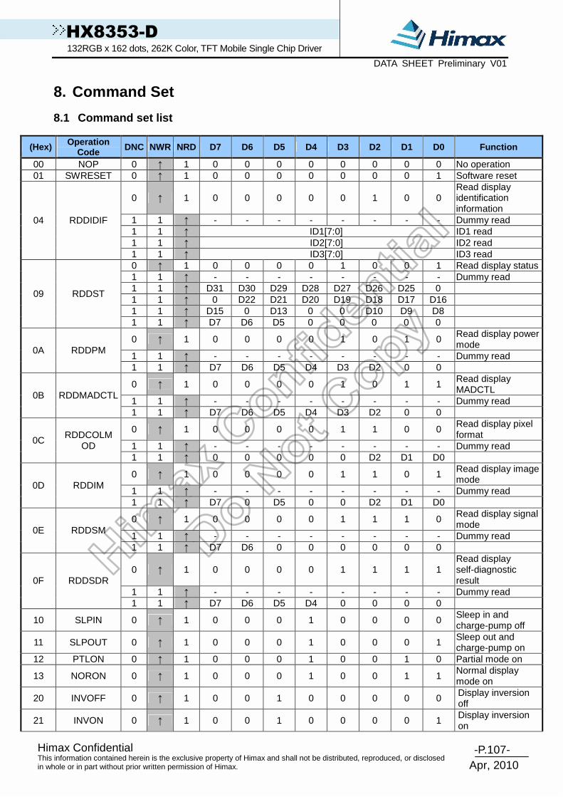
-P.107- Himax Confidential
Apr, 2010
This information contained herein is the exclusive property of Himax and shall not be distributed, reproduced, or disclosed in whole or in part without prior written permission of Himax.
HX8353-D 132RGB x 162 dots, 262K Color, TFT Mobile Single Chip Driver DATA SHEET Preliminary V01
8. Command Set 8.1 Command set list
(Hex) Operation Code DNC NWR NRD D7 D6 D5 D4 D3 D2 D1 D0 Function
00 NOP 0 ↑ 1 0 0 0 0 0 0 0 0 No operation 01 SWRESET 0 ↑ 1 0 0 0 0 0 0 0 1 Software reset
0 ↑ 1 0 0 0 0 0 1 0 0 Read display identification information
1 1 ↑ - - - - - - - - Dummy read 1 1 ↑ ID1[7:0] ID1 read 1 1 ↑ ID2[7:0] ID2 read
04 RDDIDIF
1 1 ↑ ID3[7:0] ID3 read 0 ↑ 1 0 0 0 0 1 0 0 1 Read display status 1 1 ↑ - - - - - - - - Dummy read 1 1 ↑ D31 D30 D29 D28 D27 D26 D25 0 1 1 ↑ 0 D22 D21 D20 D19 D18 D17 D16 1 1 ↑ D15 0 D13 0 0 D10 D9 D8
09 RDDST
1 1 ↑ D7 D6 D5 0 0 0 0 0
0 ↑ 1 0 0 0 0 1 0 1 0 Read display power mode
1 1 ↑ - - - - - - - - Dummy read 0A RDDPM
1 1 ↑ D7 D6 D5 D4 D3 D2 0 0
0 ↑ 1 0 0 0 0 1 0 1 1 Read display MADCTL
1 1 ↑ - - - - - - - - Dummy read 0B RDDMADCTL
1 1 ↑ D7 D6 D5 D4 D3 D2 0 0
0 ↑ 1 0 0 0 0 1 1 0 0 Read display pixel format
1 1 ↑ - - - - - - - - Dummy read 0C
RDDCOLM OD
1 1 ↑ 0 0 0 0 0 D2 D1 D0
0 ↑ 1 0 0 0 0 1 1 0 1 Read display image mode
1 1 ↑ - - - - - - - - Dummy read 0D RDDIM
1 1 ↑ D7 0 D5 0 0 D2 D1 D0
0 ↑ 1 0 0 0 0 1 1 1 0 Read display signal mode
1 1 ↑ - - - - - - - - Dummy read 0E RDDSM
1 1 ↑ D7 D6 0 0 0 0 0 0
0 ↑ 1 0 0 0 0 1 1 1 1 Read display self-diagnostic result
1 1 ↑ - - - - - - - - Dummy read 0F RDDSDR
1 1 ↑ D7 D6 D5 D4 0 0 0 0
10 SLPIN 0 ↑ 1 0 0 0 1 0 0 0 0 Sleep in and charge-pump off
11 SLPOUT 0 ↑ 1 0 0 0 1 0 0 0 1 Sleep out and charge-pump on
12 PTLON 0 ↑ 1 0 0 0 1 0 0 1 0 Partial mode on
13 NORON 0 ↑ 1 0 0 0 1 0 0 1 1 Normal display mode on
20 INVOFF 0 ↑ 1 0 0 1 0 0 0 0 0 Display inversion off
21 INVON 0 ↑ 1 0 0 1 0 0 0 0 1 Display inversion on
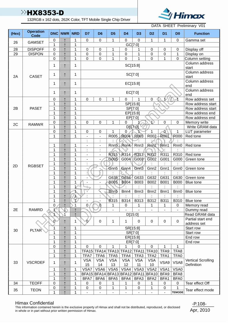
-P.108- Himax Confidential
Apr, 2010
This information contained herein is the exclusive property of Himax and shall not be distributed, reproduced, or disclosed in whole or in part without prior written permission of Himax.
HX8353-D 132RGB x 162 dots, 262K Color, TFT Mobile Single Chip Driver DATA SHEET Preliminary V01
(Hex) Operation Code DNC NWR NRD D7 D6 D5 D4 D3 D2 D1 D0 Function
0 ↑ 1 0 0 1 0 0 1 1 0 Gamma set 26 GAMSET
1 ↑ 1 GC[7:0] 28 DISPOFF 0 ↑ 1 0 0 1 0 1 0 0 0 Display off 29 DISPON 0 ↑ 1 0 0 1 0 1 0 0 1 Display on
0 ↑ 1 0 0 1 0 1 0 1 0 Column setting
1 ↑ 1 SC[15:8] Column address start
1 ↑ 1 SC[7:0] Column address start
1 ↑ 1 EC[15:8] Column address end
2A CASET
1 ↑ 1 EC[7:0] Column address end
0 ↑ 1 0 0 1 0 1 0 1 1 Row address set 1 ↑ 1 SP[15:8] Row address start 1 ↑ 1 SP[7:0] Row address start 1 ↑ 1 EP[15:8] Row address end
2B PASET
1 ↑ 1 EP[7:0] Row address end 0 ↑ 1 0 0 1 0 1 1 0 0 Memory write
2C RAMWR 1 ↑ 1 D[17:0] Write GRAM data 0 ↑ 1 0 0 1 0 1 1 0 1 LUT parameter 1 ↑ 1 - - R005 R004 R003 R002 R001 R000 Red tone : : : : : : : : 1 ↑ 1 - - Rnn5 Rnn4 Rnn3 Rnn2 Rnn1 Rnn0 Red tone 1 ↑ 1 : : : : : : : : 1 ↑ 1 - - R315 R314 R313 R312 R311 R310 Red tone 1 ↑ 1 - - G005 G004 G003 G002 G001 G000 Green tone 1 ↑ 1 : : : : : : : : 1 ↑ 1 - - Gnn5 Gnn4 Gnn3 Gnn2 Gnn1 Gnn0 Green tone 1 ↑ 1 : : : : : : : : 1 ↑ 1 - - G635 G634 G633 G632 G631 G630 Green tone 1 ↑ 1 - - B005 B004 B003 B002 B001 B000 Blue tone 1 ↑ 1 : : : : : : : : 1 ↑ 1 - - Bnn5 Bnn4 Bnn3 Bnn2 Bnn1 Bnn0 Blue tone 1 ↑ 1 : : : : : : : :
2D RGBSET
1 ↑ 1 - - B315 B314 B313 B312 B311 B310 Blue tone 0 ↑ 1 0 0 1 0 1 1 1 0 Memory read 1 1 ↑ - - - - - - - - Dummy read 2E RAMRD 1 1 ↑ D[15:0] Read GRAM data
0 ↑ 1 0 0 1 1 0 0 0 0 Partial start end address set
1 ↑ 1 SR[15:8] Start row 1 ↑ 1 SR[7:0] Start row 1 ↑ 1 ER[15:8] End row
30 PLTAR
1 ↑ 1 ER[7:0] End row 0 ↑ 1 0 0 1 1 0 0 1 1 1 ↑ 1 TFA15 TFA14 TFA13 TFA12 TFA11 TFA10 TFA9 TFA8 1 ↑ 1 TFA7 TFA6 TFA5 TFA4 TFA3 TFA2 TFA1 TFA0
1 ↑ 1 VSA 15
VSA 14
VSA 13
VSA 12
VSA 11
VSA 10
VSA9 VSA8
1 ↑ 1 VSA7 VSA6 VSA5 VSA4 VSA3 VSA2 VSA1 VSA0 1 ↑ 1 BFA15 BFA14 BFA13 BFA12 BFA11 BFA10 BFA9 BFA8
33 VSCRDEF
1 ↑ 1 BFA7 BFA6 BFA5 BFA4 BFA3 BFA2 BFA1 BFA0
Vertical Scrolling Definition
34 TEOFF 0 ↑ 1 0 0 1 1 0 1 0 0 Tear effect Off 0 ↑ 1 0 0 1 1 0 1 0 1
35 TEON 1 ↑ 1 - - - - - - - TEMODE
Tear effect mode

-P.109- Himax Confidential
Apr, 2010
This information contained herein is the exclusive property of Himax and shall not be distributed, reproduced, or disclosed in whole or in part without prior written permission of Himax.
HX8353-D 132RGB x 162 dots, 262K Color, TFT Mobile Single Chip Driver DATA SHEET Preliminary V01
(Hex) Operation Code DNC NWR NRD D7 D6 D5 D4 D3 D2 D1 D0 Function
0 ↑ 1 0 0 1 1 0 1 1 0 Memory access control 36 MADCTL
1 ↑ 1 MY MX MV ML BGR SS 0 0
0 ↑ 1 0 0 1 1 0 1 1 1 Vertical scrolling start address
1 ↑ 1 VSP 15
VSP 14
VSP 13
VSP 12
VSP 11
VSP 10
VSP9 VSP8 37 VSCRSADD
1 ↑ 1 VSP7 VSP6 VSP5 VSP4 VSP3 VSP2 VSP1 VSP0 38 IDMOFF 0 ↑ 1 0 0 1 1 1 0 0 0 Idle mode off 39 IDMON 0 ↑ 1 0 0 1 1 1 0 0 1 Idle mode on
0 ↑ 1 0 0 1 1 1 0 1 0 Interface pixel format 3A COLMOD
1 ↑ 1 0 0 0 0 0 D2 D1 D0 0 ↑ 1 1 1 0 1 1 0 1 0 Read ID1 1 1 ↑ - - - - - - - - Dummy read DA RDID1 1 1 ↑ module’s manufacturer[7:0] 0 ↑ 1 1 1 0 1 1 0 1 1 Read ID2 1 1 ↑ - - - - - - - - Dummy read DB RDID2 1 1 ↑ 1 LCD module/driver version [6:0] 0 ↑ 1 1 1 0 1 1 1 0 0 Read ID3 1 1 ↑ - - - - - - - - Dummy read DC RDID3 1 1 ↑ LCD module/driver ID[7:0]
Table 8.1 System interface command set

-P.110- Himax Confidential
Apr, 2010
This information contained herein is the exclusive property of Himax and shall not be distributed, reproduced, or disclosed in whole or in part without prior written permission of Himax.
HX8353-D 132RGB x 162 dots, 262K Color, TFT Mobile Single Chip Driver DATA SHEET Preliminary V01
Extended command set
(Hex) Operation Code DNC NWR NRD D15-8 D7 D6 D5 D4 D3 D2 D1 D0 Function
0 ↑ 1 - 1 0 1 1 0 0 0 0
1 ↑ 1 - I_RADJ[1:0] (11)
- - N_RADJ[1:0
] (10)
- - B0 SETOSC
1 ↑ 1 - - - - - - - - OSC_
EN (0)
Set internal Oscillator
0 ↑ 1 - 1 0 1 1 0 0 0 1
1 ↑ 1 - - - - - - - DP_S
TB (0)
DP_STB_S
(0) 1 ↑ 1 - - - - - - BT[2:0](001) 1 ↑ 1 - - - VRH[5:0](01_1011) 1 ↑ 1 - - - - - - AP[2:0](011) 1 ↑ 1 - FS0[7:0](0000_0100) 1 ↑ 1 - FS1[7:0](0000_1000) 1 ↑ 1 - - - - - - - - -
B1 SETPWCTR
1 ↑ 1 - GAS EN(1)
VCOMG(0) - PON
(0) DK(1) - - STB (1)
Set power control
0 ↑ 1 - 1 0 1 1 0 0 1 0 1 ↑ 1 - - - - - ISC[3:0] (0001)
1 ↑ 1 - PT[1:0] (10) PTV[1:0](01) - - PTG (1)
REF (1)
B2 SETDISPLAY
1 ↑ 1 - - - GON (1)
DTE (0) D[1:0] (00) - -
Set display control
0 ↑ 1 - 1 0 1 1 0 1 0 0 1 ↑ 1 - - I_NW[2:0](000) - N_NW[2:0](001) 1 ↑ 1 - I_RTN[3:0](0000) N_RTN[3:0](0100) 1 ↑ 1 - I_DIV[3:0](1111) N_DIV[3:0](1111) 1 ↑ 1 - N_DUM[7:0] (0000_1100) 1 ↑ 1 - I_DUM[7:0] (0000_1100) 1 ↑ 1 - GDON[7:0] (0000_1101) 1 ↑ 1 - GDOF[7:0] (0101_0011)
B4 SETCYC
1 ↑ 1 - L_BASE[7:0](0101_1001)
Set display cycle
0 ↑ 1 - 1 0 1 1 0 1 0 1
1 ↑ 1 - FBOFF(0) - -
DDVDH_TRI
(0) VVDHS_SEL[3:0] (1011)
1 ↑ 1 - - - - - VREF[3:0] (1011)
B5 SETBGP
1 ↑ 1 - - - - - VR_TRIM[3:0] (1000)
Set power control
0 ↑ 1 - 1 0 1 1 0 1 1 0 1 ↑ 1 - VMF[7:0](1001_1110) 1 ↑ 1 - VMH[7:0](0110_1100)
B6 SETVCOM
1 ↑ 1 - VML[7:0](0101_0100)
Set VCOM voltage
0 ↑ 1 - 1 0 1 1 1 0 0 1 1 ↑ 1 - EXTC1[7:0] (0000_0000) 1 ↑ 1 - EXTC2[7:0] (0000_0000)
B9 SETEXTC
1 ↑ 1 - EXTC3[7:0] (0000_0000)
Enter extension command
0 ↑ 1 - 1 0 1 1 1 0 1 1 Set OTP 1 ↑ 1 - OTP_MASK[7:0] (0000_0000) 1 ↑ 1 - OTP_INDEX[7:0] (0000_0000)
1 ↑ 1 -
OTP_LOAD_ DISAB
LE (0)
DCCLK_
DISABLE (0)
OTP_ POR (0)
OTP_PWE (0)
OTP_EN (0)
OTPTEST_EN
(0)
VPP_SEL(0)
OTP_PROG(0
)
1 ↑ 1 - - - - - OTP_PTM [1:0](00)
OTP_VRADJ [1:0](00)
BB SETOTP
1 1 ↑ OTP_DATA[7:0] (0000_0000)

-P.111- Himax Confidential
Apr, 2010
This information contained herein is the exclusive property of Himax and shall not be distributed, reproduced, or disclosed in whole or in part without prior written permission of Himax.
HX8353-D 132RGB x 162 dots, 262K Color, TFT Mobile Single Chip Driver DATA SHEET Preliminary V01
(Hex) Operation Code DNC NWR NRD D15-8 D7 D6 D5 D4 D3 D2 D1 D0 Function
0 ↑ 1 - 1 1 0 0 0 0 0 0 1 ↑ 1 - N_OPON[7:0] (0001_1000) 1 ↑ 1 - I_OPON[7:0] (0000_1000) 1 ↑ 1 - STBA[15:8] (0000_1100) 1 ↑ 1 - STBA[7:0] (1100_0100) 1 ↑ 1 - GENON[7:0] (0001_0000)
C0 SETSTBA
1 ↑ 1 - - - - - - - - OTPS1B (0)
Set Source option
0 ↑ 1 - 1 1 0 0 0 0 1 1 1 ↑ 1 - ID1[7:0] (0000_0000) 1 ↑ 1 - ID2[7:0] (1000_0000)
C3 SETID
1 ↑ 1 - ID3[7:0] (0000_0000)
Set ID
0 ↑ 1 1 1 0 0 0 1 1 0 C6 SETUADJ
1 ↑ 1 - I_UADJ[2:0](011) - N_UADJ[2:0](001) Set UADJ to trimming Freq
SETCLOCK 0 ↑ 1 1 1 0 0 1 0 1 1 1 ↑ 1 CADJ[3:0] (0010) - - - -
CB 1 ↑ 1
- - - - - - -
DCCLK_SYNC(1)
0 ↑ 1 - 1 1 0 0 1 1 0 0
CC SETPANEL 1 ↑ 1 - - - - -
SS_PANEL
(0)
GS_PANEL
(0)
REV_PANEL(0)
BGR_PANEL(0)
Set Panel characteristics
0 1 ↑ 1 1 0 1 0 0 0 0 1 1 ↑ Dummy Read D0 GETHID 1 1 ↑ Product ID[7:0] (0110_0100)
Read Product ID
0 ↑ 1 - 1 1 1 0 0 0 0 0 1 ↑ 1 - - MP1[2:0](000) - MP0[2:0](000) 1 ↑ 1 - - MP3[2:0](110) - MP2[2:0](101) 1 ↑ 1 - - MP5[2:0](111) - MP4[2:0](001) 1 ↑ 1 - - - - - CP0[3:0](1010) 1 ↑ 1 - CP2[3:0](1111) CP1[3:0](0111) 1 ↑ 1 - - - - - CP3[3:0](0001) 1 ↑ 1 - - - - - CP4[3:0](1100) 1 ↑ 1 - - - - - OP0[3:0](1111) 1 ↑ 1 - - - - OP1[4:0](0_0000) 1 ↑ 1 - - - - - CGM1[1:0](11) CGM0[1:0](00) 1 ↑ 1 - - MN1[2:0](101) - MN0[2:0](000) 1 ↑ 1 - - MN3[2:0](010) - MN2[2:0](001) 1 ↑ 1 - - MN5[2:0](111) - MN4[2:0](111) 1 ↑ 1 - - - - - CN0[3:0](1100) 1 ↑ 1 - CN2[3:0](1111) CN1[3:0](0001) 1 ↑ 1 - - - - - CN3[3:0](0111) 1 ↑ 1 - - - - - CN4[3:0](1010) 1 ↑ 1 - - - - - ON0[3:0](0000)
E0 SETGAMMA
1 ↑ 1 - - - - ON1[4:0](0_1111)
Set Gamma
0 ↑ 1 - 1 1 1 0 0 0 1 1 1 ↑ 1 - EQVCI_M1[7:0] (0001_0000) 1 ↑ 1 - EQGND_M1[7:0](0000_1000) 1 ↑ 1 - EQVCI_M0[7:0](0000_1000) 1 ↑ 1 - EQGND_M0[7:0](0001_0000) 1 ↑ 1 - PREOE_M0[7:0](0000_0000)
E3 SETEQ
1 ↑ 1 - PREOE_M1[7:0](0000_0000)
Set EQ
Table 8.2 System Interface In-House Command Set

-P.112- Himax Confidential
Apr, 2010
This information contained herein is the exclusive property of Himax and shall not be distributed, reproduced, or disclosed in whole or in part without prior written permission of Himax.
HX8353-D 132RGB x 162 dots, 262K Color, TFT Mobile Single Chip Driver DATA SHEET Preliminary V01
8.2 Command description 8.2.1 NOP
00 H NOP (No Operation) DNC NWR NRD D17-8 D7 D6 D5 D4 D3 D2 D1 D0 HEX Command 0 ↑ 1 - 0 0 0 0 0 0 0 0 00 Parameter NO PARAMETER
Description This command is an empty command; it does not have any effect on the display module. However it can be used to terminate Frame Memory Write as described in RAMWR (Memory Write) or RAMRD (Memory Read) command.
Restriction
Register Availability
Status Availability Normal Mode On, Idle Mode Off, Sleep Out Yes Normal Mode On, Idle Mode On, Sleep Out Yes Partial Mode On, Idle Mode Off, Sleep Out Yes Partial Mode On, Idle Mode On, Sleep Out Yes
Sleep In or Booster Off Yes
Default
Status Default Value Power On Sequence N/A
S/W Reset N/A H/W Reset N/A
Flow Chart -

-P.113- Himax Confidential
Apr, 2010
This information contained herein is the exclusive property of Himax and shall not be distributed, reproduced, or disclosed in whole or in part without prior written permission of Himax.
HX8353-D 132RGB x 162 dots, 262K Color, TFT Mobile Single Chip Driver DATA SHEET Preliminary V01
8.2.2 Software reset (01h)
01 H SWRESET (Software Reset) DNC NWR NRD D17-8 D7 D6 D5 D4 D3 D2 D1 D0 HEX Command 0 ↑ 1 - 0 0 0 0 0 0 0 1 01 Parameter NO PARAMETER
Description
When the Software Reset command is written, it causes a software reset. It resets the commands and parameters to their S/W Reset default values. (See default tables in each command description.) The display is blank immediately. Note: The GRAM contents are unaffected by this command.
Restriction
It will be necessary to wait 5m sec before sending new command following software reset. The display module loads all display suppliers’ factory default values to the registers during this 5m sec. If SW Reset is applied during Sleep Out mode, it will be necessary to wait 120m sec before sending Sleep Out command. SW Reset command cannot be sent during Sleep Out sequence.
Register Availability
Status Availability Normal Mode On, Idle Mode Off, Sleep Out Yes Normal Mode On, Idle Mode On, Sleep Out Yes Partial Mode On, Idle Mode Off, Sleep Out Yes Partial Mode On, Idle Mode On, Sleep Out Yes
Sleep In or Booster Off Yes
Default
Status Default Value Power On Sequence N/A
S/W Reset N/A H/W Reset N/A
Flow Chart
Legend
Parameter
Display
Action
Mode
Sequentialtransfer

-P.114- Himax Confidential
Apr, 2010
This information contained herein is the exclusive property of Himax and shall not be distributed, reproduced, or disclosed in whole or in part without prior written permission of Himax.
HX8353-D 132RGB x 162 dots, 262K Color, TFT Mobile Single Chip Driver DATA SHEET Preliminary V01
8.2.3 Read display identification information (04h)
04 H RDDIDIF (Read Display Identification Information) DNC NWR NRD D17-8 D7 D6 D5 D4 D3 D2 D1 D0 HEX Command 0 ↑ 1 - 0 0 0 0 0 1 0 0 04
1st parameter 1 1 ↑ - - - - - - - - - - 2nd parameter 1 1 ↑ - ID17 ID16 ID15 ID14 ID13 ID12 ID11 ID10 - 3rd parameter 1 1 ↑ - ID27 ID26 ID25 ID24 ID23 ID22 ID21 ID20 - 4th parameter 1 1 ↑ - ID37 ID36 ID35 ID34 ID33 ID32 ID31 ID30 -
Description
This read byte returns 24-bit display identification information. The 1st Parameter is dummy read. The 2nd ~ 4th Parameter identifies the LCD module’s manufacturer. It is defined by display supplier and it changes each time a revision is made to the display, material or construction specifications. See Table:
ID Byte Value ID2[7:0] Version Changes 80h - - 81h - - 82h - - 83h - - 84h - - 85h - -
The 4th parameter identifies the LCD module/driver. Restriction -
Register Availability
Status Availability Normal Mode On, Idle Mode Off, Sleep Out Yes Normal Mode On, Idle Mode On, Sleep Out Yes Partial Mode On, Idle Mode Off, Sleep Out Yes Partial Mode On, Idle Mode On, Sleep Out Yes
Sleep In or Booster Off Yes
Default
Status Default Value Power On Sequence See Description
S/W Reset See Description H/W Reset See Description

-P.115- Himax Confidential
Apr, 2010
This information contained herein is the exclusive property of Himax and shall not be distributed, reproduced, or disclosed in whole or in part without prior written permission of Himax.
HX8353-D 132RGB x 162 dots, 262K Color, TFT Mobile Single Chip Driver DATA SHEET Preliminary V01
Flow Chart

-P.116- Himax Confidential
Apr, 2010
This information contained herein is the exclusive property of Himax and shall not be distributed, reproduced, or disclosed in whole or in part without prior written permission of Himax.
HX8353-D 132RGB x 162 dots, 262K Color, TFT Mobile Single Chip Driver DATA SHEET Preliminary V01
8.2.4 Read display status (09h)
09 H RDDST (Read Display Status) DNC NWR NRD D17-8 D7 D6 D5 D4 D3 D2 D1 D0 HEX Command 0 ↑ 1 - 0 0 0 0 1 0 0 1 09
1st parameter 1 1 ↑ - - - - - - - - - - 2nd parameter 1 1 ↑ - D31 D30 D29 D28 D27 D26 D25 0 - 3rd parameter 1 1 ↑ - 0 D22 D21 D20 D19 D18 D17 D16 - 4th parameter 1 1 ↑ - D15 0 D13 0 0 D10 D9 D8 - 5th parameter 1 1 ↑ - D7 D6 D5 D4 D3 D2 D1 0 -
Description
This command indicates the current status of the display as described in the table below:
Bit Description Comment D31 Booster Voltage Status - D30 Page Address Order (MY) - D29 Column Address Order (MX) - D28 Page/Column Order (MV) - D27 Line Address Order (ML) - D26 RGB/BGR Order - D25 Display Data Latch Order - D24 Switching between Segment outputs and RAM Set to ‘0’ D23 Switching between Common outputs and RAM Set to ‘0’ D22 - D21 - D20
Interface Color Pixel Format Definition -
D19 Idle Mode On/Off - D18 Partial Mode On/Off - D17 Sleep In/Out - D16 Display Normal Mode On/Off - D15 Vertical Scrolling Status - D14 Horizontal Scrolling Status Set to ‘0’ D13 Inversion Status - D12 All Pixels On Set to ‘0’ D11 All Pixels Off Set to ‘0’ D10 Display On/Off - D9 Tearing Effect Line On/Off - D8 - D7 - D6
Gamma Curve Selection -
D5 Tearing Effect Output Line Mode - D4 Horizontal Sync. (HS, RGB I/F) Set to ‘0’ D3 Vertical Sync. (VS,RGB I/F) Set to ‘0’ D2 Pixel Clock (DOTCLK,RGB I/F)) Set to ‘0’ D1 Data Enable (DE,RGB I/F) Set to ‘0’ D0 Parity Error Set to ‘0’
Bit Values are explained overleaf. Bit D31 – Booster Voltage Status
‘0’ = Booster Off or has a fault. ‘1’ = Booster On and working OK.
Bit D30 – Page Address Order ‘0’ = Top to Bottom (When MADCTL B7(MY) = ’0’). ‘1’ = Bottom to Top (When MADCTL B7(MY) =’1’).
Bit D29 – Column Address Order ‘0’ = Left to Right (When MADCTL B6(MX) = ’0’). ‘1’ = Right to Left (When MADCTL B6(MX) = ’1’).
Bit D28 –Page / Column Order ‘0’ = Normal Mode (When MADCTL B5(MV) = ’0’).

-P.117- Himax Confidential
Apr, 2010
This information contained herein is the exclusive property of Himax and shall not be distributed, reproduced, or disclosed in whole or in part without prior written permission of Himax.
HX8353-D 132RGB x 162 dots, 262K Color, TFT Mobile Single Chip Driver DATA SHEET Preliminary V01
‘1’ = Reverse Mode (When MADCTL B5(MV) = ’1’). Bit D27 – Line Address Order
‘0’ = LCD Refresh Top to Bottom (When MADCTL B4(ML) = ’0’). ‘1’ = LCD Refresh Bottom to Top (When MADCTL B4(ML) = ’1’).
Bit D26 – RGB/BGR Order ‘0’ = RGB (When MADCTL B3 = ’0’). ‘1’ = BGR (When MADCTL B3 = ’1’).
Bit D25 – Display Data Latch Order ‘0’ = LCD Refresh Left to Right (When MADCTL B2 = ’0’). ‘1’ = LCD Refresh Right to Left (When MADCTL B2 = ’1’).
Note : For bits D27, D26 and D25 also refer to 8.3.29 Memory Access Control (R36h) Bit D24 – Switching Between Segment Outputs and RAM
This bit is not applicable for this project, so it is set to ‘0’. Bit D23 – Switching Between Common Outputs and RAM
This bit is not applicable for this project, so it is set to ‘0’. Bits D22, D21, D20 –Interface Color Pixel Format Definition
Interface Format D22 D21 D20
Not Defined 0 0 0 Not Defined 0 0 1
Not Defined 0 1 0
12 bit/pixel 0 1 1 Not Defined 1 0 0
16 bit/pixel 1 0 1
18 bit/pixel 1 1 0
Not Defined 1 1 1
Bit D19 – Idle Mode On/Off ‘0’ = Idle Mode Off. ‘1’ = Idle Mode On.
Bit D18 – Partial Mode On/Off ‘0’ = Partial Mode Off. ‘1’ = Partial Mode On.
Bit D17 – Sleep In/Out ‘0’ = Sleep In Mode. ‘1’ = Sleep Out Mode.
Bit D16 – Display Normal Mode On/Off ‘0’ = Display Normal Mode Off. ‘1’ = Display Normal Mode On.
Bit D15 – Vertical Scrolling On/Off ‘0’ = Vertical Scrolling is Off. ‘1’ = Vertical Scrolling is On.
Bit D14 – Horizontal Scrolling Status This bit is not applicable for this project, so it is set to ‘0’. Bit D13 – Inversion On/Off
‘0’ = Inversion is Off. ‘1’ = Inversion is On.
Bit D12 – All Pixels On This bit is not applicable for this project, so it is set to ‘0’.
Bit D11 – All Pixels Off This bit is not applicable for this project, so it is set to ‘0’.
Bit D10 – Display On/Off ‘0’ = Display is Off. ‘1’ = Display is On.
Bit D9 – Tearing Effect Line On/Off ‘0’ =Tearing Effect Line Off. ‘1’ = Tearing Effect On.

-P.118- Himax Confidential
Apr, 2010
This information contained herein is the exclusive property of Himax and shall not be distributed, reproduced, or disclosed in whole or in part without prior written permission of Himax.
HX8353-D 132RGB x 162 dots, 262K Color, TFT Mobile Single Chip Driver DATA SHEET Preliminary V01
Bits D8, D7, D6 – Gamma Curve Selection Gamma Curve Selected B8 B7 B6 Gamma Set (26h) Parameter Gamma Curve 1 0 0 0 GC0 Gamma Curve 2 0 0 1 GC1 Gamma Curve 3 0 1 0 GC2 Gamma Curve 4 0 1 1 GC3 Not Defined 1 0 0 Not Defined Not Defined 1 0 1 Not Defined Not Defined 1 1 0 Not Defined Not Defined 1 1 1 Not Defined
Bit D5 – Tearing Effect Line Output Mode.
‘0’ = Mode 1, V-Blanking only. ‘1’ = Mode 2, both H-Blanking and V-Blanking.
Bit D4 – Horizontal Sync. (HS) RGB I/F On/Off, Note This bit is not applicable for this project, so it is set to ‘0’.
Bit D3 – Vertical Sync. (VS) RGB I/F On/Off, Note This bit is not applicable for this project, so it is set to ‘0’.
Bit D2 – Pixel Clock (DOTCLK) RGB I/F On/Off, Note This bit is not applicable for this project, so it is set to ‘0’.
Bit D1 – Data Enable (DE) RGB I/F On/Off, Note This bit is not applicable for this project, so it is set to ‘0’.
Bit D0 – Parity Error This bit is not applicable for this project, so it is set to ‘0’.
Restriction -
Register Availability
Status Availability Normal Mode On, Idle Mode Off, Sleep Out Yes Normal Mode On, Idle Mode On, Sleep Out Yes Partial Mode On, Idle Mode Off, Sleep Out Yes Partial Mode On, Idle Mode On, Sleep Out Yes
Sleep In or Booster Off Yes
Default
Status Default Value Power On Sequence See Description
S/W Reset See Description H/W Reset See Description
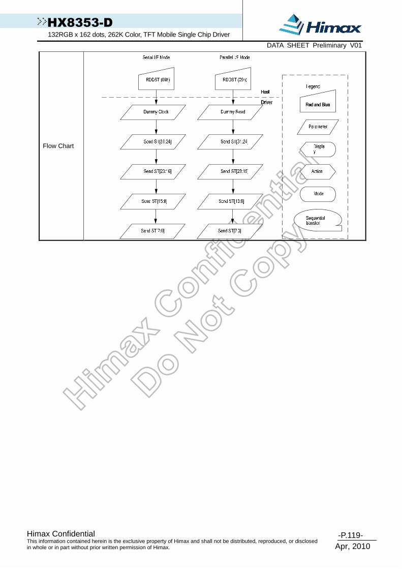
-P.119- Himax Confidential
Apr, 2010
This information contained herein is the exclusive property of Himax and shall not be distributed, reproduced, or disclosed in whole or in part without prior written permission of Himax.
HX8353-D 132RGB x 162 dots, 262K Color, TFT Mobile Single Chip Driver DATA SHEET Preliminary V01
Flow Chart

-P.120- Himax Confidential
Apr, 2010
This information contained herein is the exclusive property of Himax and shall not be distributed, reproduced, or disclosed in whole or in part without prior written permission of Himax.
HX8353-D 132RGB x 162 dots, 262K Color, TFT Mobile Single Chip Driver DATA SHEET Preliminary V01
8.2.5 Read display power mode (0Ah)
0A H RDDPM (Read Display Power Mode) DNC NWR NRD D15-8 D7 D6 D5 D4 D3 D2 D1 D0 HEX Command 0 ↑ 1 - 0 0 0 0 1 0 1 0 0A 1st parameter 1 1 ↑ - - - - - - - - - - 2nd parameter 1 1 ↑ - D7 D6 D5 D4 D3 D2 0 0 xx
Description
This command indicates the current status of the display as described in the table below:
Bit Description Comment D7 Booster Voltage Status - D6 Idle Mode On/Off - D5 Partial Mode On/Off - D4 Sleep In/Out - D3 Display Normal Mode On/Off - D2 Display On/Off - D1 Not Defined Set to ‘0’ D0 Not Defined Set to ‘0’
Bit D7 – Booster Voltage Status ‘0’ = Booster Off or has a fault. ‘1’ = Booster On and working OK (Meets display supplier’s optical requirements).
Bit D6 – Idle Mode On/Off ‘0’ = Idle Mode Off. ‘1’ = Idle Mode On.
Bit D5 – Partial Display Mode On/Off ‘0’ = Partial Mode Off. ‘1’ = Partial Mode On.
Bit D4 – Sleep In/Out ‘0’ = Sleep In Mode. ‘1’ = Sleep Out Mode.
Bit D3 – Normal Display Mode On/Off ‘0’ = Display Normal Mode Off. ‘1’ = Display Normal Mode On.
Bit D2 – Display On/Off ‘0’ = Display is Off. ‘1’ = Display is On.
Bit D1 – Not Defined This bit is not applicable for this project, so it is set to ‘0’. Bit D0 – Not Defined This bit is not applicable for this project, so it is set to ‘0’.
Restrictions -
Register Availability
Status Availability Normal Mode On, Idle Mode Off, Sleep Out Yes Normal Mode On, Idle Mode On, Sleep Out Yes Partial Mode On, Idle Mode Off, Sleep Out Yes Partial Mode On, Idle Mode On, Sleep Out Yes
Sleep In or Booster Off Yes
Default
Status Default Value Power On Sequence 08h
S/W Reset 08h H/W Reset 08h

-P.121- Himax Confidential
Apr, 2010
This information contained herein is the exclusive property of Himax and shall not be distributed, reproduced, or disclosed in whole or in part without prior written permission of Himax.
HX8353-D 132RGB x 162 dots, 262K Color, TFT Mobile Single Chip Driver DATA SHEET Preliminary V01
Flow Chart
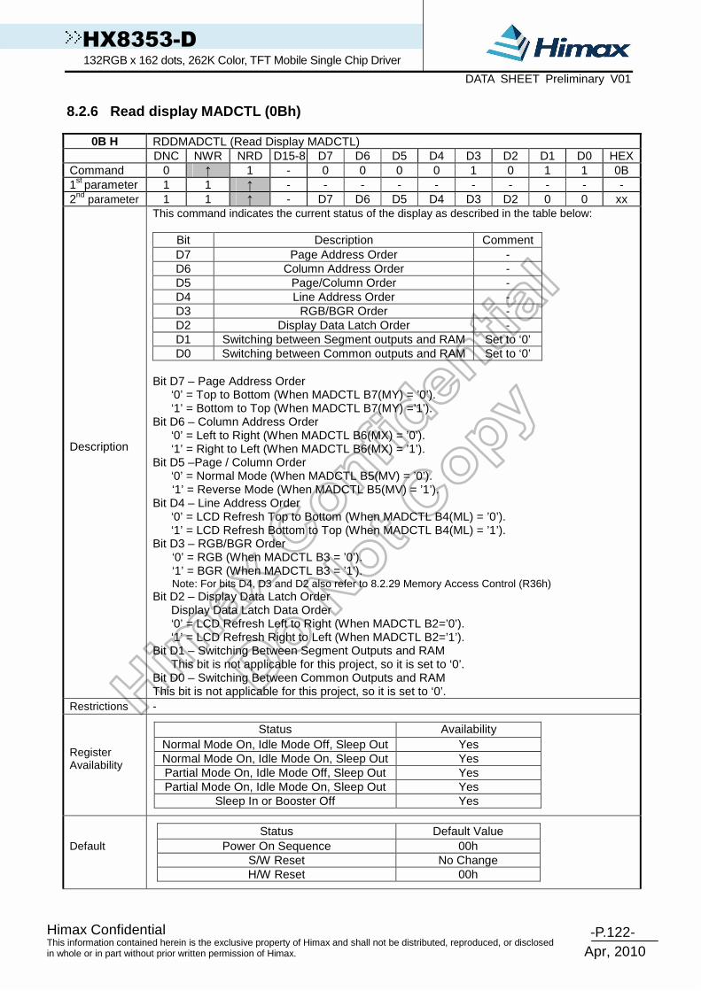
-P.122- Himax Confidential
Apr, 2010
This information contained herein is the exclusive property of Himax and shall not be distributed, reproduced, or disclosed in whole or in part without prior written permission of Himax.
HX8353-D 132RGB x 162 dots, 262K Color, TFT Mobile Single Chip Driver DATA SHEET Preliminary V01
8.2.6 Read display MADCTL (0Bh)
0B H RDDMADCTL (Read Display MADCTL) DNC NWR NRD D15-8 D7 D6 D5 D4 D3 D2 D1 D0 HEX Command 0 ↑ 1 - 0 0 0 0 1 0 1 1 0B 1st parameter 1 1 ↑ - - - - - - - - - - 2nd parameter 1 1 ↑ - D7 D6 D5 D4 D3 D2 0 0 xx
Description
This command indicates the current status of the display as described in the table below:
Bit Description Comment D7 Page Address Order - D6 Column Address Order - D5 Page/Column Order - D4 Line Address Order - D3 RGB/BGR Order - D2 Display Data Latch Order - D1 Switching between Segment outputs and RAM Set to ‘0’ D0 Switching between Common outputs and RAM Set to ‘0’
Bit D7 – Page Address Order
‘0’ = Top to Bottom (When MADCTL B7(MY) = ’0’). ‘1’ = Bottom to Top (When MADCTL B7(MY) =’1’).
Bit D6 – Column Address Order ‘0’ = Left to Right (When MADCTL B6(MX) = ’0’). ‘1’ = Right to Left (When MADCTL B6(MX) = ’1’).
Bit D5 –Page / Column Order ‘0’ = Normal Mode (When MADCTL B5(MV) = ’0’). ‘1’ = Reverse Mode (When MADCTL B5(MV) = ’1’).
Bit D4 – Line Address Order ‘0’ = LCD Refresh Top to Bottom (When MADCTL B4(ML) = ’0’). ‘1’ = LCD Refresh Bottom to Top (When MADCTL B4(ML) = ’1’).
Bit D3 – RGB/BGR Order ‘0’ = RGB (When MADCTL B3 = ’0’). ‘1’ = BGR (When MADCTL B3 = ’1’). Note: For bits D4, D3 and D2 also refer to 8.2.29 Memory Access Control (R36h)
Bit D2 – Display Data Latch Order Display Data Latch Data Order ‘0’ = LCD Refresh Left to Right (When MADCTL B2=’0’). ‘1’ = LCD Refresh Right to Left (When MADCTL B2=’1’).
Bit D1 – Switching Between Segment Outputs and RAM This bit is not applicable for this project, so it is set to ‘0’.
Bit D0 – Switching Between Common Outputs and RAM This bit is not applicable for this project, so it is set to ‘0’.
Restrictions -
Register Availability
Status Availability Normal Mode On, Idle Mode Off, Sleep Out Yes Normal Mode On, Idle Mode On, Sleep Out Yes Partial Mode On, Idle Mode Off, Sleep Out Yes Partial Mode On, Idle Mode On, Sleep Out Yes
Sleep In or Booster Off Yes
Default
Status Default Value Power On Sequence 00h
S/W Reset No Change H/W Reset 00h

-P.123- Himax Confidential
Apr, 2010
This information contained herein is the exclusive property of Himax and shall not be distributed, reproduced, or disclosed in whole or in part without prior written permission of Himax.
HX8353-D 132RGB x 162 dots, 262K Color, TFT Mobile Single Chip Driver DATA SHEET Preliminary V01
Flow Chart

-P.124- Himax Confidential
Apr, 2010
This information contained herein is the exclusive property of Himax and shall not be distributed, reproduced, or disclosed in whole or in part without prior written permission of Himax.
HX8353-D 132RGB x 162 dots, 262K Color, TFT Mobile Single Chip Driver DATA SHEET Preliminary V01
8.2.7 Read display pixel format (0Ch)
0C H RDDCOLMOD (Read Display COLMOD) DNC NWR NRD D15-8 D7 D6 D5 D4 D3 D2 D1 D0 HEX Command 0 ↑ 1 - 0 0 0 0 1 1 0 0 0C 1st parameter 1 1 ↑ - - - - - - - - - - 2nd parameter 1 1 ↑ - 0 D6 D5 D4 0 D2 D1 D0 xx
Description
This command indicates the current status of the display as described in the table below: Bit Description Comment D7 Set to ‘0’ D6 Set to ‘0’ D5 Set to ‘0’ D4
RGB Interface Color Format
Set to ‘0’ D3 Set to ‘0’ D2 - D1 - D0
System Interface Color Format
- Bit D7 – RGB Interface Color Format Selection
This bit is not applicable for this project, so it is set to ‘0’. Bits D6, D5, D4 – RGB Interface Color Pixel Format Definition
These bits are not applicable for this project, so they are set to ‘0’s. Bit D3 – System Interface Color Format Selection
This bit is not applicable for this project, so it is set to ‘0’. Bit D2, D1, D0 – Control Interface Color Pixel Format Definition.
See section“8.2.33 Interface Pixel Format (R3Ah)”.
System Interface Color Format D2 D1 D0
Not Defined 0 0 0 Not Defined 0 0 1 Not Defined 0 1 0 Not Defined 0 1 1 Not Defined 1 0 0 16 bit/pixel 1 0 1 18 bit/pixel 1 1 0 Not Defined 1 1 1
Restrictions -
Register Availability
Status Availability Normal Mode On, Idle Mode Off, Sleep Out Yes Normal Mode On, Idle Mode On, Sleep Out Yes Partial Mode On, Idle Mode Off, Sleep Out Yes Partial Mode On, Idle Mode On, Sleep Out Yes
Sleep In or Booster Off Yes
Default
Status Default Value Power On Sequence 18-bit/pixel
S/W Reset No Change H/W Reset 18-bit/pixel

-P.125- Himax Confidential
Apr, 2010
This information contained herein is the exclusive property of Himax and shall not be distributed, reproduced, or disclosed in whole or in part without prior written permission of Himax.
HX8353-D 132RGB x 162 dots, 262K Color, TFT Mobile Single Chip Driver DATA SHEET Preliminary V01
Flow Chart

-P.126- Himax Confidential
Apr, 2010
This information contained herein is the exclusive property of Himax and shall not be distributed, reproduced, or disclosed in whole or in part without prior written permission of Himax.
HX8353-D 132RGB x 162 dots, 262K Color, TFT Mobile Single Chip Driver DATA SHEET Preliminary V01
8.2.8 Read display image mode (0Dh)
0D H RDDIM (Read Display Image Mode) DNC NWR NRD D15-8 D7 D6 D5 D4 D3 D2 D1 D0 HEX Command 0 ↑ 1 - 0 0 0 0 1 1 0 1 0D 1st parameter 1 1 ↑ - - - - - - - - - - 2nd parameter 1 1 ↑ - D7 0 D5 0 0 D2 D1 D0 xx
Description
This command indicates the current status of the display as described in the table below: Bit D7 – Vertical Scrolling On/Off ‘0’ = Vertical Scrolling is Off. ‘1’ = Vertical Scrolling is On. Bit D6 – Horizontal Scrolling Status This bit is not applicable for this project, so it is set to ‘0’ Bit D5 – Inversion On/Off ‘0’ = Inversion is Off. ‘1’ = Inversion is On. This bit is not applicable for this project, so it is set to ‘0’ Bit D4 – All Pixels On This bit is not applicable for this project, so it is set to ‘0’ Bit D3 – All Pixels Off This bit is not applicable for this project, so it is set to ‘0’ Bits D2, D1, D0 – Gamma Curve Selection
Gamma Curve Selected D2 D1 D0 Gamma Set (R26h) Parameter Gamma Curve 1 0 0 0 GC0 Gamma Curve 2 0 0 1 GC1 Gamma Curve 3 0 1 0 GC2 Gamma Curve 4 0 1 1 GC3 Not Defined 1 0 0 Not Defined Not Defined 1 0 1 Not Defined Not Defined 1 1 0 Not Defined Not Defined 1 1 1 Not Defined
Restrictions -
Register Availability
Status Availability Normal Mode On, Idle Mode Off, Sleep Out Yes Normal Mode On, Idle Mode On, Sleep Out Yes Partial Mode On, Idle Mode Off, Sleep Out Yes Partial Mode On, Idle Mode On, Sleep Out Yes
Sleep In or Booster Off Yes
Default
Status Default Value Power On Sequence 00h
S/W Reset 00h H/W Reset 00h

-P.127- Himax Confidential
Apr, 2010
This information contained herein is the exclusive property of Himax and shall not be distributed, reproduced, or disclosed in whole or in part without prior written permission of Himax.
HX8353-D 132RGB x 162 dots, 262K Color, TFT Mobile Single Chip Driver DATA SHEET Preliminary V01
Flow Chart

-P.128- Himax Confidential
Apr, 2010
This information contained herein is the exclusive property of Himax and shall not be distributed, reproduced, or disclosed in whole or in part without prior written permission of Himax.
HX8353-D 132RGB x 162 dots, 262K Color, TFT Mobile Single Chip Driver DATA SHEET Preliminary V01
8.2.9 Read display signal mode (0Eh)
0E H RDDSM (Read Display Signal Mode) DNC NWR NRD D15-8 D7 D6 D5 D4 D3 D2 D1 D0 HEX Command 0 ↑ 1 - 0 0 0 0 1 1 1 0 0E 1st parameter 1 1 ↑ - - - - - - - - - - 2nd parameter 1 1 ↑ - D7 D6 D5 D4 D3 D2 0 0 xx
Description
This command indicates the current status of the display as described in the table below: Bit D7 – Tearing Effect Line On/Off
‘0’ = Tearing Effect Line Off. ‘1’ = Tearing Effect On.
Bit D6 – Tearing Effect Line Output Mode, see section 7.3 for mode definitions. ‘0’ = Mode 1. ‘1’ = Mode 2.
Bit D5 – Horizontal Sync. (VSYNC, RGB I/F) On/Off This bit is not applicable for this project, so it is set to ‘0’ Bit D4 – Vertical Sync. (HSYNC, RGB I/F) On/Off This bit is not applicable for this project, so it is set to ‘0’ Bit D3 – Pixel Clock (DCLK, RGB I/F) On/Off This bit is not applicable for this project, so it is set to ‘0’ Bit D2 – Data Enable (ENABLE, RGB I/F)) On/Off This bit is not applicable for this project, so it is set to ‘0’ D1 are D0 - are for future use and are set to ‘0’.
Restrictions -
Register Availability
Status Availability Normal Mode On, Idle Mode Off, Sleep Out Yes Normal Mode On, Idle Mode On, Sleep Out Yes Partial Mode On, Idle Mode Off, Sleep Out Yes Partial Mode On, Idle Mode On, Sleep Out Yes
Sleep In or Booster Off Yes
Default
Status Default Value Power On Sequence 00h
S/W Reset 00h H/W Reset 00h
Flow Chart

-P.129- Himax Confidential
Apr, 2010
This information contained herein is the exclusive property of Himax and shall not be distributed, reproduced, or disclosed in whole or in part without prior written permission of Himax.
HX8353-D 132RGB x 162 dots, 262K Color, TFT Mobile Single Chip Driver DATA SHEET Preliminary V01
8.2.10 Read display self-diagnostic result (0Fh)
0F H RDDSDR (Read Display Self-Diagnostic Result) DNC NWR NRD D15-8 D7 D6 D5 D4 D3 D2 D1 D0 HEX Command 0 ↑ 1 - 0 0 0 0 1 1 1 1 0F 1st parameter 1 1 ↑ - - - - - - - - - - 2nd parameter 1 1 ↑ - D7 D6 D5 D4 0 0 0 0 -
Description
This command indicates the status of the display self-diagnostic results after Sleep Out -command as described in the table below: Bit D7 – Register Loading Detection
See section 7.6.1. Bit D6 – Functionality Detection
See section 7.6.2. Bit D5 – Chip Attachment Detection
Set bit D5 to ‘0’, if this function is not implemented. Bit D4 – Display Glass Break Detection
Set bit D4 to ‘0’, if this function is not implemented. Bits D3, D2, D1 and D0 are for future use and are set to ‘0’.
Restrictions -
Register Availability
Status Availability Normal Mode On, Idle Mode Off, Sleep Out Yes Normal Mode On, Idle Mode On, Sleep Out Yes Partial Mode On, Idle Mode Off, Sleep Out Yes Partial Mode On, Idle Mode On, Sleep Out Yes
Sleep In or Booster Off Yes
Default
Status Default Value Power On Sequence 00h
S/W Reset 00h H/W Reset 00h
Flow Chart

-P.130- Himax Confidential
Apr, 2010
This information contained herein is the exclusive property of Himax and shall not be distributed, reproduced, or disclosed in whole or in part without prior written permission of Himax.
HX8353-D 132RGB x 162 dots, 262K Color, TFT Mobile Single Chip Driver DATA SHEET Preliminary V01
8.2.11 Sleep in (10h)
10 H SLPIN (Sleep In) DNC NWR NRD D15-8 D7 D6 D5 D4 D3 D2 D1 D0 HEX Command 0 ↑ 1 - 0 0 0 1 0 0 0 0 10 Parameter NO PARAMETER
Description
This command causes the LCD module to enter the minimum power consumption mode. In this mode the DC/DC converter is stopped, Internal oscillator is stopped, and panel scanning is stopped.
MCU interface and memory are still working and the memory keeps its contents.
Restriction
This command has no effect when module is already in sleep in mode. Sleep In Mode can only be left by the Sleep Out Command (11h). It will be necessary to wait 5msec before sending next command, this is to allow time for the supply voltages and clock circuits to stabilize. It will be necessary to wait 120msec after sending Sleep Out command (when in Sleep In Mode) before Sleep In command can be sent.
Register Availability
Status Availability Normal Mode On, Idle Mode Off, Sleep Out Yes Normal Mode On, Idle Mode On, Sleep Out Yes Partial Mode On, Idle Mode Off, Sleep Out Yes Partial Mode On, Idle Mode On, Sleep Out Yes
Sleep In or Booster Off Yes
Default
Status Default Value Power On Sequence Sleep In Mode
S/W Reset Sleep In Mode H/W Reset Sleep In Mode
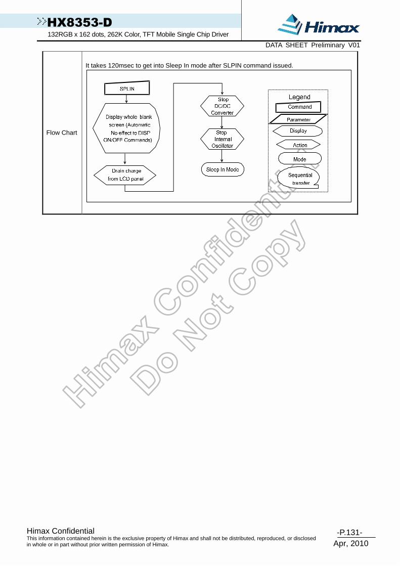
-P.131- Himax Confidential
Apr, 2010
This information contained herein is the exclusive property of Himax and shall not be distributed, reproduced, or disclosed in whole or in part without prior written permission of Himax.
HX8353-D 132RGB x 162 dots, 262K Color, TFT Mobile Single Chip Driver DATA SHEET Preliminary V01
Flow Chart
It takes 120msec to get into Sleep In mode after SLPIN command issued.

-P.132- Himax Confidential
Apr, 2010
This information contained herein is the exclusive property of Himax and shall not be distributed, reproduced, or disclosed in whole or in part without prior written permission of Himax.
HX8353-D 132RGB x 162 dots, 262K Color, TFT Mobile Single Chip Driver DATA SHEET Preliminary V01
8.2.12 Sleep out (11h)
11 H SLPOUT (Sleep Out) DNC NWR NRD D15-8 D7 D6 D5 D4 D3 D2 D1 D0 HEX Command 0 ↑ 1 - 0 0 0 1 0 0 0 1 11 Parameter NO PARAMETER
Description
This command turns off sleep mode. In this mode the DC/DC converter is enabled, Internal oscillator is started, and panel scanning is started.
Restriction
This command has no effect when module is already in sleep out mode. Sleep Out Mode can only be left by the Sleep In Command (10h). It will be necessary to wait 5msec before sending next command, this is to allow time for the supply voltages and clock circuits to stabilize. The display module loads all display suppliers’ factory default values to the registers during this 5msec and there cannot be any abnormal visual effect on the display image. If factory default and register values are same when this load is done and when the display module is already Sleep Out –mode. The display module is doing self-diagnostic functions during this 5msec. It will be necessary to wait 120msec after sending Sleep In command (when in Sleep Out mode) before Sleep Out command can be sent.
Register Availability
Status Availability Normal Mode On, Idle Mode Off, Sleep Out Yes Normal Mode On, Idle Mode On, Sleep Out Yes Partial Mode On, Idle Mode Off, Sleep Out Yes Partial Mode On, Idle Mode On, Sleep Out Yes
Sleep In or Booster Off Yes
Default
Status Default Value Power On Sequence Sleep In Mode
S/W Reset Sleep In Mode H/W Reset Sleep In Mode
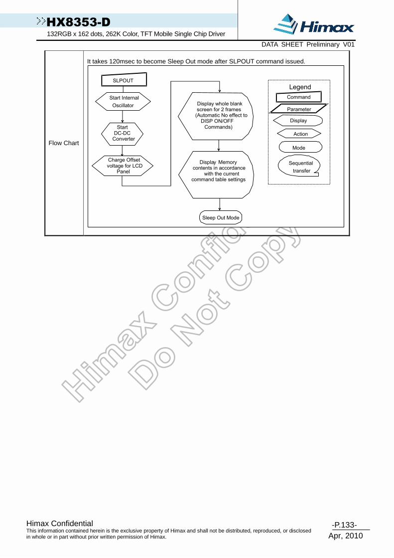
-P.133- Himax Confidential
Apr, 2010
This information contained herein is the exclusive property of Himax and shall not be distributed, reproduced, or disclosed in whole or in part without prior written permission of Himax.
HX8353-D 132RGB x 162 dots, 262K Color, TFT Mobile Single Chip Driver DATA SHEET Preliminary V01
Flow Chart
It takes 120msec to become Sleep Out mode after SLPOUT command issued.
Legend
Command
Parameter
Display
Action
Mode
Sequential
transfer
SLPOUT
Charge Offsetvoltage for LCD
Panel
Sleep Out Mode
Start Internal
Oscillator
StartDC-DCConverter
Display whole blankscreen for 2 frames(Automatic No effect to
DISP ON/OFFCommands)
Display Memorycontents in accordance
with the currentcommand table settings

-P.134- Himax Confidential
Apr, 2010
This information contained herein is the exclusive property of Himax and shall not be distributed, reproduced, or disclosed in whole or in part without prior written permission of Himax.
HX8353-D 132RGB x 162 dots, 262K Color, TFT Mobile Single Chip Driver DATA SHEET Preliminary V01
8.2.13 Partial mode on (12h)
12 H PTLON (Partial Mode On) DNC NWR NRD D15-8 D7 D6 D5 D4 D3 D2 D1 D0 HEX Command 0 ↑ 1 - 0 0 0 1 0 0 1 0 12 Parameter NO PARAMETER
Description
This command turns on partial mode The partial mode window is described by the Partial Area command (30H). To leave Partial mode, the Normal Display Mode On command (13H) should be written. See also section 6.3.8
Restrictions This command has no effect when Partial mode is active.
Register Availability
Status Availability Normal Mode On, Idle Mode Off, Sleep Out Yes Normal Mode On, Idle Mode On, Sleep Out Yes Partial Mode On, Idle Mode Off, Sleep Out Yes Partial Mode On, Idle Mode On, Sleep Out Yes
Sleep In or Booster Off Yes
Default
Status Default Value Power On Sequence Normal Display Mode On
S/W Reset Normal Display Mode On H/W Reset Normal Display Mode On
Flow Chart See Partial Area (30h)

-P.135- Himax Confidential
Apr, 2010
This information contained herein is the exclusive property of Himax and shall not be distributed, reproduced, or disclosed in whole or in part without prior written permission of Himax.
HX8353-D 132RGB x 162 dots, 262K Color, TFT Mobile Single Chip Driver DATA SHEET Preliminary V01
8.2.14 Normal display mode on (13h)
13 H NORON (Normal Display Mode On) DNC NWR NRD D15-8 D7 D6 D5 D4 D3 D2 D1 D0 HEX
Command 0 ↑ 1 - 0 0 0 1 0 0 1 1 13 Parameter NO PARAMETER
Description This command returns the display to normal mode. Normal display mode on means Partial mode off, Scroll mode Off. See also section 6.2.1.
Restriction This command has no effect when Normal mode is active.
Register Availability
Status Availability Normal Mode On, Idle Mode Off, Sleep Out Yes Normal Mode On, Idle Mode On, Sleep Out Yes Partial Mode On, Idle Mode Off, Sleep Out Yes Partial Mode On, Idle Mode On, Sleep Out Yes
Sleep In or Booster Off Yes
Default
Status Default Value Power On Sequence Normal Display Mode On
S/W Reset Normal Display Mode On H/W Reset Normal Display Mode On
Flow Chart See Partial Area and Vertical Scrolling Definition Descriptions for details of when to use this command.

-P.136- Himax Confidential
Apr, 2010
This information contained herein is the exclusive property of Himax and shall not be distributed, reproduced, or disclosed in whole or in part without prior written permission of Himax.
HX8353-D 132RGB x 162 dots, 262K Color, TFT Mobile Single Chip Driver DATA SHEET Preliminary V01
8.2.15 Display inversion off (20h)
20 H INVOFF (Display Inversion Off) DNC NRD NWR D15-8 D7 D6 D5 D4 D3 D2 D1 D0 HEX Command 0 1 ↑ - 0 0 1 0 0 0 0 0 20 Parameter NO PARAMETER
Description
This command is used to recover from display inversion mode. This command makes no change of contents of frame memory. This command does not change any other status.
Restriction -
Register Availability
Status Availability Normal Mode On, Idle Mode Off, Sleep Out Yes Normal Mode On, Idle Mode On, Sleep Out Yes Partial Mode On, Idle Mode Off, Sleep Out Yes Partial Mode On, Idle Mode On, Sleep Out Yes
Sleep In or Booster Off Yes
Default
Status Default Value Power On Sequence Display Inversion Off
S/W Reset Display Inversion Off H/W Reset Display Inversion Off
Flow Chart

-P.137- Himax Confidential
Apr, 2010
This information contained herein is the exclusive property of Himax and shall not be distributed, reproduced, or disclosed in whole or in part without prior written permission of Himax.
HX8353-D 132RGB x 162 dots, 262K Color, TFT Mobile Single Chip Driver DATA SHEET Preliminary V01
8.2.16 Display inversion on (21h)
21 H INVON (Display Inversion On) DNC NRD NWR D15-8 D7 D6 D5 D4 D3 D2 D1 D0 HEX Command 0 1 ↑ - 0 0 1 0 0 0 0 1 21 Parameter NO PARAMETER
Description
This command is used to enter into display inversion mode. This command makes no change of contents of frame memory. Every bit is inverted from the frame memory to the display. This command does not change any other status.
Restriction
Register Availability
Status Availability Normal Mode On, Idle Mode Off, Sleep Out Yes Normal Mode On, Idle Mode On, Sleep Out Yes Partial Mode On, Idle Mode Off, Sleep Out Yes Partial Mode On, Idle Mode On, Sleep Out Yes
Sleep In or Booster Off Yes
Default
Status Default Value Power On Sequence Display Inversion Off
S/W Reset Display Inversion Off H/W Reset Display Inversion Off
Flow Chart

-P.138- Himax Confidential
Apr, 2010
This information contained herein is the exclusive property of Himax and shall not be distributed, reproduced, or disclosed in whole or in part without prior written permission of Himax.
HX8353-D 132RGB x 162 dots, 262K Color, TFT Mobile Single Chip Driver DATA SHEET Preliminary V01
8.2.17 Gamma set (26h)
26 H GAMSET (Gamma Set) DNC NWR NRD D15-8 D7 D6 D5 D4 D3 D2 D1 D0 HEX Command 0 ↑ 1 - 0 0 1 0 0 1 1 0 26 Parameter 1 ↑ 1 - GC7 GC6 GC5 GC4 GC3 GC2 GC1 GC0 -
Description
This command is used to select the desired Gamma curve for the current display. A maximum of 4 fixed gamma curves can be selected. The curve is selected by setting the appropriate bit in the parameter as described in the table:
GC[7..0] Parameter Curve Selected 01h GC0 Gamma Curve 1 02h GC1 Gamma Curve 2 04h GC2 Gamma Curve 3 08h GC3 Gamma Curve 4
Note: All other values are undefined.
Restriction
Values of GC[7..0] not shown in table above are invalid and will not change the Current selected Gamma curve until valid value is received.
Register Availability
Status Availability Normal Mode On, Idle Mode Off, Sleep Out Yes Normal Mode On, Idle Mode On, Sleep Out Yes Partial Mode On, Idle Mode Off, Sleep Out Yes Partial Mode On, Idle Mode On, Sleep Out Yes
Sleep In or Booster Off Yes
Default
Status Default Value Power On Sequence 01h
S/W Reset 01h H/W Reset 01h
Flow Chart
Legend
Command
Parameter
Display
Action
Mode
Sequential
transfer
GAMSET
GC [7:0]
New Gamma
Curve Loaded

-P.139- Himax Confidential
Apr, 2010
This information contained herein is the exclusive property of Himax and shall not be distributed, reproduced, or disclosed in whole or in part without prior written permission of Himax.
HX8353-D 132RGB x 162 dots, 262K Color, TFT Mobile Single Chip Driver DATA SHEET Preliminary V01
8.2.18 Display off (28h)
28 H DISPOFF (Display Off) DNC NWR NRD D15-8 D7 D6 D5 D4 D3 D2 D1 D0 HEX
Command 0 ↑ 1 - 0 0 1 0 1 0 0 0 28 Parameter NO PARAMETER
Description
This command is used to enter into DISPLAY OFF mode. In this mode, the output from Frame Memory is disabled and blank page inserted. This command makes no change of contents of frame memory. This command does not change any other status. There will be no abnormal visible effect on the display.
Restriction This command has no effect when module is already in display off mode.
Register Availability
Status Availability Normal Mode On, Idle Mode Off, Sleep Out Yes Normal Mode On, Idle Mode On, Sleep Out Yes Partial Mode On, Idle Mode Off, Sleep Out Yes Partial Mode On, Idle Mode On, Sleep Out Yes
Sleep In or Booster Off Yes
Default
Status Default Value Power On Sequence Display Off
S/W Reset Display Off H/W Reset Display Off
Flow Chart
-P.140- Himax Confidential
Apr, 2010
This information contained herein is the exclusive property of Himax and shall not be distributed, reproduced, or disclosed in whole or in part without prior written permission of Himax.
HX8353-D 132RGB x 162 dots, 262K Color, TFT Mobile Single Chip Driver DATA SHEET Preliminary V01
8.2.19 Display on (29h)
29 H DISPON (Display On) DNC NWR NRD D15-8 D7 D6 D5 D4 D3 D2 D1 D0 HEX Command 0 ↑ 1 - 0 0 1 0 1 0 0 1 29 Parameter NO PARAMETER
Description
This command is used to recover from DISPLAY OFF mode. Output from the Frame Memory is enabled. This command makes no change of contents of frame memory. This command does not change any other status.
Restriction This command has no effect when module is already in display on mode.
Register Availability
Status Availability Normal Mode On, Idle Mode Off, Sleep Out Yes Normal Mode On, Idle Mode On, Sleep Out Yes Partial Mode On, Idle Mode Off, Sleep Out Yes Partial Mode On, Idle Mode On, Sleep Out Yes
Sleep In or Booster Off Yes
Default
Status Default Value Power On Sequence Display Off
S/W Reset Display Off H/W Reset Display Off
Flow Chart

-P.141- Himax Confidential
Apr, 2010
This information contained herein is the exclusive property of Himax and shall not be distributed, reproduced, or disclosed in whole or in part without prior written permission of Himax.
HX8353-D 132RGB x 162 dots, 262K Color, TFT Mobile Single Chip Driver DATA SHEET Preliminary V01
8.2.20 Column address set (2Ah)
2A H CASET (Column Address Set) DNC NWR NRD D15-8 D7 D6 D5 D4 D3 D2 D1 D0 HEX Command 0 ↑ 1 - 0 0 1 0 1 0 1 0 2A 1st parameter 1 ↑ 1 - SC15 SC14 SC13 SC12 SC11 SC10 SC9 SC8 2nd parameter 1 ↑ 1 - SC7 SC6 SC5 SC4 SC3 SC2 SC1 SC0
Note
3rd parameter 1 ↑ 1 - EC15 EC14 EC13 EC12 EC11 EC10 EC9 EC8 4th parameter 1 ↑ 1 - EC7 EC6 EC5 EC4 EC3 EC2 EC1 EC0
Note
Description
This command is used to define area of frame memory where MCU can access. This command makes no change on the other driver status. The values of SC[15:0] and EC[15:0] are referred when RAMWR command comes. Each value represents one column line in the Frame Memory.
Restriction
SC[15:0] always must be equal to or less than EC[15:0] Note: When SC[15:0] or EC[15:0] is greater than maximum address like below, data out of range
will be ignored 0000h<=SC[15:0]<=EC[15:0] <=0083h ,when MADCTL’s B5=0 0000h<=SC[15:0]<=EC[15:0] <=00A1h ,when MADCTL’s B5=1
Register Availability
Status Availability Normal Mode On, Idle Mode Off, Sleep Out Yes Normal Mode On, Idle Mode On, Sleep Out Yes Partial Mode On, Idle Mode Off, Sleep Out Yes Partial Mode On, Idle Mode On, Sleep Out Yes
Sleep In or Booster Off Yes
Default
Status Default Value Power On Sequence SC[15:0]=0000h EC[15:0]=0083h
When MADCTL’s B5=0: SC[15:0]=0000h EC[15:0]=0083h
When MADCTL’s B5=1: S/W Reset
SC[15:0]=0000h EC[15:0]=00A1h H/W Reset SC[15:0]=0000h EC[15:0]=0083h
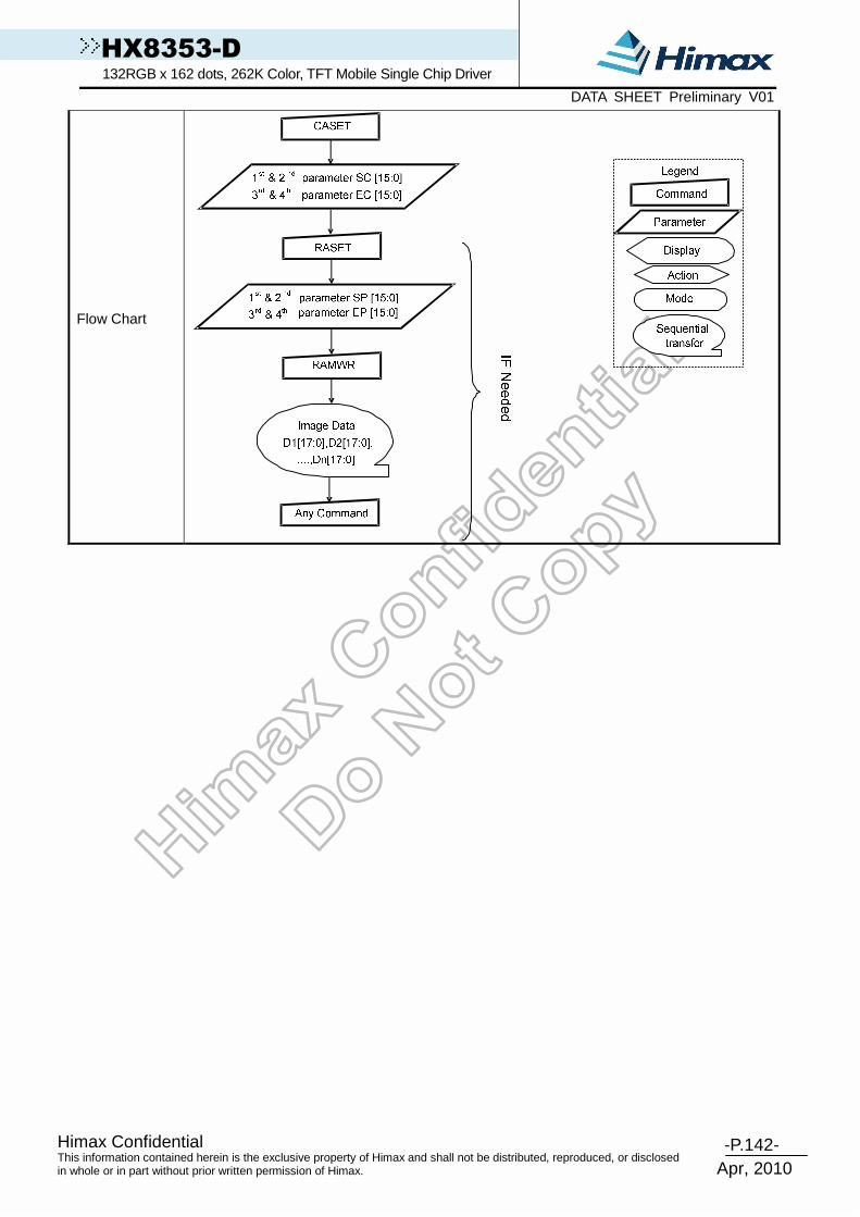
-P.142- Himax Confidential
Apr, 2010
This information contained herein is the exclusive property of Himax and shall not be distributed, reproduced, or disclosed in whole or in part without prior written permission of Himax.
HX8353-D 132RGB x 162 dots, 262K Color, TFT Mobile Single Chip Driver DATA SHEET Preliminary V01
Flow Chart

-P.143- Himax Confidential
Apr, 2010
This information contained herein is the exclusive property of Himax and shall not be distributed, reproduced, or disclosed in whole or in part without prior written permission of Himax.
HX8353-D 132RGB x 162 dots, 262K Color, TFT Mobile Single Chip Driver DATA SHEET Preliminary V01
8.2.21 Page address set (2Bh) 2B H PASET (Page Address Set) DNC NWR NRD D15-8 D7 D6 D5 D4 D3 D2 D1 D0 HEX Command 0 ↑ 1 - 0 0 1 0 1 0 1 1 2B 1st parameter 1 ↑ 1 - SP15 SP14 SP13 SP12 SP11 SP10 SP9 SP8 2nd parameter 1 ↑ 1 - SP7 SP6 SP5 SP4 SP3 SP2 SP1 SP0
Note
3rd parameter 1 ↑ 1 - EP15 EP14 EP13 EP12 EP11 EP10 EP9 EP8 4th parameter 1 ↑ 1 - EP7 EP6 EP5 EP4 EP3 EP2 EP1 EP0
Note
Description
This command is used to define area of frame memory where MCU can access. This command makes no change on the other driver status. The values of SP[15:0] and EP[15:0] are referred when RAMWR command comes. Each value represents one Page line in the Frame Memory.
Restriction
SP[15:0] always must be equal to or less than EP[15:0] Note: When SP[15:0] or EP[15:0] is greater than maximum row address like below, data of out of
range will be ignored 0000h<=SP[15:0]<=EP[15:0]<=00A1h (When MADCTL’s B5=0) 0000h<=SP[15:0]<=EP[15:0]<=0083h (When MADCTL’s B5=1)
Register Availability
Status Availability Normal Mode On, Idle Mode Off, Sleep Out Yes Normal Mode On, Idle Mode On, Sleep Out Yes Partial Mode On, Idle Mode Off, Sleep Out Yes Partial Mode On, Idle Mode On, Sleep Out Yes
Sleep In or Booster Off Yes
Default
Status Default Value Power On Sequence SP[15:0]=0000h EP[15:0]=00A1h
When MADCTL’s B5=0: SP[15:0]=0000h EP[15:0]=00A1h
When MADCTL’s B5=1: S/W Reset
SP[15:0]=0000h EP[15:0]=0083h H/W Reset SP[15:0]=0000h EP[15:0]=00A1h

-P.144- Himax Confidential
Apr, 2010
This information contained herein is the exclusive property of Himax and shall not be distributed, reproduced, or disclosed in whole or in part without prior written permission of Himax.
HX8353-D 132RGB x 162 dots, 262K Color, TFT Mobile Single Chip Driver DATA SHEET Preliminary V01
Flow Chart
IF Needed
Legend
Command
Parameter
Display
Action
Mode
Sequential
transfer
CASET
RASET
RAMWR
Image Data
D1[17:0],D2[17:0],
...,Dn[17:0]
Any Command
1st & 2
nd parameter SP [15:0]
3rd & 4
th parameter EP [15:0]
1st & 2
nd parameter SC [15:0]
3rd & 4
th parameter EC [15:0]
IF Needed

-P.145- Himax Confidential
Apr, 2010
This information contained herein is the exclusive property of Himax and shall not be distributed, reproduced, or disclosed in whole or in part without prior written permission of Himax.
HX8353-D 132RGB x 162 dots, 262K Color, TFT Mobile Single Chip Driver DATA SHEET Preliminary V01
8.2.22 Memory write (2Ch)
2C H RAMWR (Memory Write) DNC NWR NRD D15-8 D7 D6 D5 D4 D3 D2 D1 D0 HEX Command 0 ↑ 1 - 0 0 1 0 1 1 0 0 2C 1st parameter 1 ↑ 1 D1[15:0] 00..FF
: 1 ↑ 1 Dx[15:0] 00..FF nth parameter 1 ↑ 1 Dn[15:0] 00..FF
Description
This command is used to transfer data from MCU to frame memory. This command makes no change to the other driver status. When this command is accepted, the column register and the page register are reset to the Start Column/Start Page positions. The Start Column/Start Page positions are different in accordance with MADCTL setting. (See 6.2) Then D[7:0] is stored in frame memory and the column register and the page register incremented. Sending any other command can stop frame Write.
Restriction In all color modes, there is no restriction on length of parameters.
Register Availability
Status Availability Normal Mode On, Idle Mode Off, Sleep Out Yes Normal Mode On, Idle Mode On, Sleep Out Yes Partial Mode On, Idle Mode Off, Sleep Out Yes Partial Mode On, Idle Mode On, Sleep Out Yes
Sleep In or Booster Off Yes
Default
Status Default Value Power On Sequence Contents of memory is set randomly
S/W Reset Contents of memory is not cleared H/W Reset Contents of memory is not cleared
Flow Chart

-P.146- Himax Confidential
Apr, 2010
This information contained herein is the exclusive property of Himax and shall not be distributed, reproduced, or disclosed in whole or in part without prior written permission of Himax.
HX8353-D 132RGB x 162 dots, 262K Color, TFT Mobile Single Chip Driver DATA SHEET Preliminary V01
8.2.23 Color set (2Dh) 2D H RGBSET (Color Set) DNC NRD NWR DB7 DB6 DB5 DB4 DB3 DB2 DB1 DB0 HEX Command 0 1 ↑ 0 0 1 0 1 1 0 1 2D 1st parameter 1 1 ↑ X X R005 R004 R003 R002 R001 R000 00..FF
: 1 1 ↑ X X Rnn5 Rnn4 Rnn3 Rnn2 Rnn1 Rnn0 00..FF 32th parameter 1 1 ↑ X X R315 R314 R313 R312 R311 R310 00..FF 33rd parameter 1 1 ↑ X X G005 G004 G003 G002 G001 G000 00..FF
: 1 1 ↑ X X Gnn5 Gnn4 Gnn3 Gnn2 Gnn1 Gnn0 00..FF 96th parameter 1 1 ↑ X X G635 G634 G633 G632 G631 G630 00..FF 97th parameter 1 1 ↑ X X B005 B004 B003 B002 B001 B000 00..FF
: 1 1 ↑ X X Bnn5 Bnn4 Bnn3 Bnn2 Bnn1 Bnn0 00..FF 128th parameter 1 1 ↑ X X B315 B314 B313 B312 B311 B310 00..FF
Description
This command is used to define the LUT for 12bit-to-18bit/16bit-to-18bit color depth conversions. (See also section 5.2) 128 bytes must be written to the LUT regardless of the color mode. This command has no effect on other commands/parameters and Contents of frame memory. Visible change takes effect next time the Frame Memory is written to.
Restriction -
Register Availability
Status Availability Normal Mode On, Idle Mode Off, Sleep Out Yes Normal Mode On, Idle Mode On, Sleep Out Yes Partial Mode On, Idle Mode Off, Sleep Out Yes Partial Mode On, Idle Mode On, Sleep Out Yes Sleep In or Booster Off Yes
Default
Status Default Value Power On Sequence Random values S/W Reset Contents of the look-up table protected H/W Reset Random values
Flow Chart
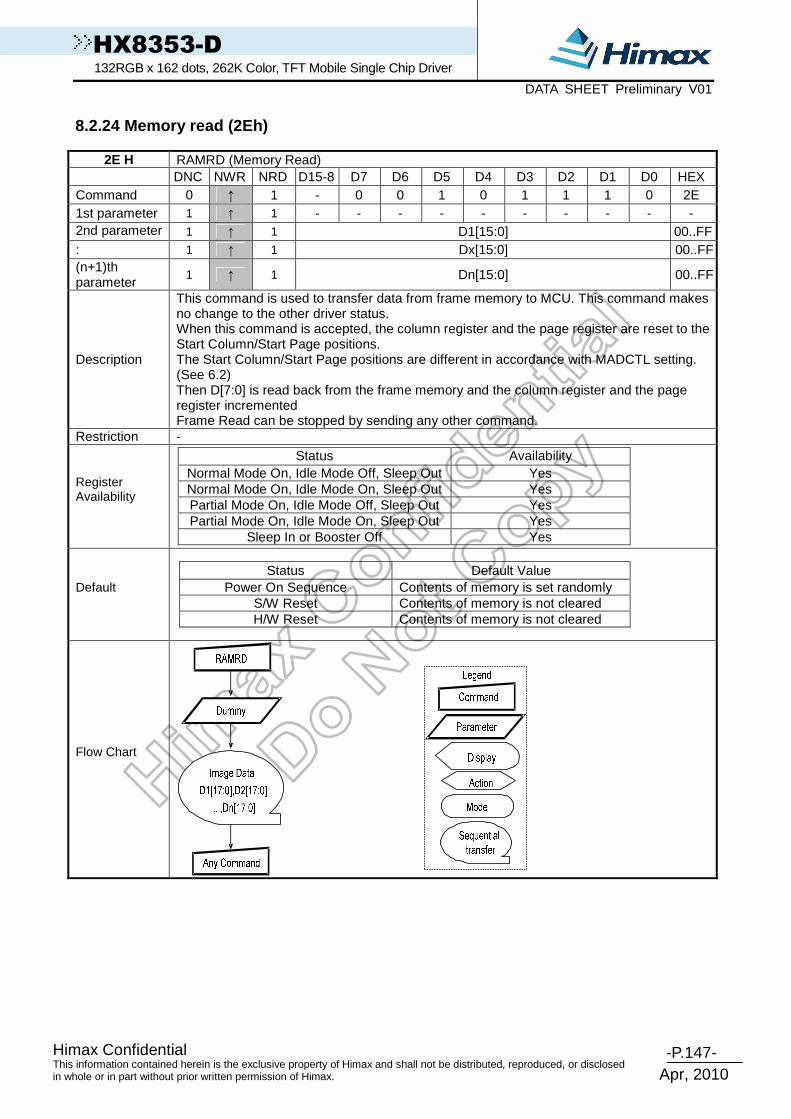
-P.147- Himax Confidential
Apr, 2010
This information contained herein is the exclusive property of Himax and shall not be distributed, reproduced, or disclosed in whole or in part without prior written permission of Himax.
HX8353-D 132RGB x 162 dots, 262K Color, TFT Mobile Single Chip Driver DATA SHEET Preliminary V01
8.2.24 Memory read (2Eh)
2E H RAMRD (Memory Read) DNC NWR NRD D15-8 D7 D6 D5 D4 D3 D2 D1 D0 HEX Command 0 ↑ 1 - 0 0 1 0 1 1 1 0 2E 1st parameter 1 ↑ 1 - - - - - - - - - - 2nd parameter 1 ↑ 1 D1[15:0] 00..FF : 1 ↑ 1 Dx[15:0] 00..FF (n+1)th parameter
1 ↑ 1 Dn[15:0] 00..FF
Description
This command is used to transfer data from frame memory to MCU. This command makes no change to the other driver status. When this command is accepted, the column register and the page register are reset to the Start Column/Start Page positions. The Start Column/Start Page positions are different in accordance with MADCTL setting. (See 6.2) Then D[7:0] is read back from the frame memory and the column register and the page register incremented Frame Read can be stopped by sending any other command.
Restriction -
Register Availability
Status Availability Normal Mode On, Idle Mode Off, Sleep Out Yes Normal Mode On, Idle Mode On, Sleep Out Yes Partial Mode On, Idle Mode Off, Sleep Out Yes Partial Mode On, Idle Mode On, Sleep Out Yes
Sleep In or Booster Off Yes
Default
Status Default Value Power On Sequence Contents of memory is set randomly
S/W Reset Contents of memory is not cleared H/W Reset Contents of memory is not cleared
Flow Chart

-P.148- Himax Confidential
Apr, 2010
This information contained herein is the exclusive property of Himax and shall not be distributed, reproduced, or disclosed in whole or in part without prior written permission of Himax.
HX8353-D 132RGB x 162 dots, 262K Color, TFT Mobile Single Chip Driver DATA SHEET Preliminary V01
8.2.25 Partial area (30h)
30 H PLTAR (Partial Area) DNC NWR NRD D15-8 D7 D6 D5 D4 D3 D2 D1 D0 HEX Command 0 ↑ 1 - 0 0 1 1 0 0 0 0 30
1st parameter 1 ↑ 1 - SR15 SR14 SR13 SR12 SR11 SR10 SR9 SR8 2nd parameter 1 ↑ 1 - SR7 SR6 SR5 SR4 SR3 SR2 SR1 SR0
0000: 013F
3rd parameter 1 ↑ 1 - ER15 ER14 ER13 ER12 ER11 ER10 ER9 ER8 4th parameter 1 ↑ 1 - ER7 ER6 ER5 ER4 ER3 ER2 ER1 ER0
0000: 013F
Description
This command defines the partial mode’s display area. There are 4 parameters associated with this command, the first defines the Start Row (SR) and the second the End Row (ER), as illustrated in the figures below. SR and ER refer to the Frame Memory Line Pointer. If End Row > Start Row when MADCTL B4(ML) = 0:
If End Row > Start Row when MADCTL B4(ML) = 1:
If End Row<Start Row when MADCTL’s B4(ML) = 0:
SR[15:0]
Start Row
ER[15:0]
Partial
Area
End Row
If End Row = Start Row then the Partial Area will be one row deep.
Restriction SR[15:0] and ER[15:0] cannot be exceeding than 00A1h.

-P.149- Himax Confidential
Apr, 2010
This information contained herein is the exclusive property of Himax and shall not be distributed, reproduced, or disclosed in whole or in part without prior written permission of Himax.
HX8353-D 132RGB x 162 dots, 262K Color, TFT Mobile Single Chip Driver DATA SHEET Preliminary V01
Register Availability
Status Availability
Normal Mode On, Idle Mode Off, Sleep Out Yes Normal Mode On, Idle Mode On, Sleep Out Yes Partial Mode On, Idle Mode Off, Sleep Out Yes Partial Mode On, Idle Mode On, Sleep Out Yes
Sleep In or Booster Off Yes
Default
Status Default Value
Power On Sequence SR[15:0]=0000h ER[15:0]=00A1h S/W Reset SR[15:0]=0000h ER[15:0]=00A1h H/W Reset SR[15:0]=0000h ER[15:0]=00A1h
Flow Chart
1. To Enter Partial Display Mode:
2. To Leave Partial Display Mode

-P.150- Himax Confidential
Apr, 2010
This information contained herein is the exclusive property of Himax and shall not be distributed, reproduced, or disclosed in whole or in part without prior written permission of Himax.
HX8353-D 132RGB x 162 dots, 262K Color, TFT Mobile Single Chip Driver DATA SHEET Preliminary V01
8.2.26 Vertical scrolling definition (33h)
33 H VSCRDEF (Vertical Scrolling Definition) DNC NWR NRD D15-8 D7 D6 D5 D4 D3 D2 D1 D0 HEX Command 0 ↑ 1 - 0 0 1 1 0 0 1 1 33
1st parameter 1 ↑ 1 - TFA 15 TFA 14 TFA 13 TFA 12 TFA 11 TFA 10 TFA 9 TFA 8
2nd parameter 1 ↑ 1 - TFA 7 TFA 6 TFA 5 TFA 4 TFA 3 TFA 2 TFA 1 TFA 0 0000: 00A2
3rd parameter 1 ↑ 1 - VSA 15 VSA 14 VSA 13 VSA 12 VSA 11 VSA 10 VSA 9 VSA 8
4th parameter 1 ↑ 1 - VSA 7 VSA 6 VSA 5 VSA 4 VSA 3 VSA 2 VSA 1 VSA 0 0000: 00A2
5th parameter 1 ↑ 1 - BFA 15 BFA 14 BFA 13 BFA 12 BFA 11 BFA 10 BFA 9 BFA 8
6th parameter 1 ↑ 1 - BFA 7 BFA 6 BFA 5 BFA 4 BFA 3 BFA 2 BFA 1 BFA 0
0000: 00A2
Description
This command defines the Vertical Scrolling Area of the display. When MADCTL B4=0, the 1st & 2nd parameter TFA[15:0] describes the Top Fixed Area (in No. of lines from top of the Frame Memory and Display). The 3rd & 4th parameter VSA[15:0] describes the height of the Vertical Scrolling Area (in No. of lines of the Frame Memory [not the display] from the Vertical Scrolling Start Address). The first line read from Frame Memory appears immediately after the bottom most line of the Top Fixed Area. The 5th & 6th parameter BFA[15:0] describes the Bottom Fixed Area (in No. of lines from Bottom of the Frame Memory and Display). TFA, VSA and BFA refer to the Frame Memory Line Pointer.
When MADCTL B4=1 The 1st & 2nd parameter TFA[15:0] describes the Top Fixed Area (in No. of lines from bottom of the Frame Memory and Display). The 3rd & 4th parameter VSA[15:0] describes the height of the Vertical Scrolling Area (in No. of lines of the Frame Memory [not the display] from the Vertical Scrolling Start Address). The first line read from Frame Memory appears immediately after the top most line of the Top Fixed Area. The 5th & 6th parameter BFA[15:0] describes the Bottom Fixed Area (in No. of lines from Top of the Frame Memory and Display).
Restriction The condition is (TFA+VSA+BFA)=162, otherwise Scrolling mode is undefined. In Vertical Scroll Mode, MADCTL B5 should be set to ‘0’ – this only affects the Frame Memory Write.

-P.151- Himax Confidential
Apr, 2010
This information contained herein is the exclusive property of Himax and shall not be distributed, reproduced, or disclosed in whole or in part without prior written permission of Himax.
HX8353-D 132RGB x 162 dots, 262K Color, TFT Mobile Single Chip Driver DATA SHEET Preliminary V01
Register Availability
Status Availability Normal Mode On, Idle Mode Off, Sleep Out Yes Normal Mode On, Idle Mode On, Sleep Out Yes Partial Mode On, Idle Mode Off, Sleep Out Yes Partial Mode On, Idle Mode On, Sleep Out Yes
Sleep In or Booster Off Yes
Default
Status Default Value Power On Sequence TFA[15:0]=0000 VSA[15:0]=00A2h BFA[15:0]=0000 S/W Reset TFA[15:0]=0000 VSA[15:0]=00A2h BFA[15:0]=0000 H/W Reset TFA[15:0]=0000 VSA[15:0]=00A2h BFA[15:0]=0000
Flow Charts
1. To enter Vertical Scroll Mode:
Note: The Frame Memory Window size must be defined correctly otherwise undesirable image will be
displayed.

-P.152- Himax Confidential
Apr, 2010
This information contained herein is the exclusive property of Himax and shall not be distributed, reproduced, or disclosed in whole or in part without prior written permission of Himax.
HX8353-D 132RGB x 162 dots, 262K Color, TFT Mobile Single Chip Driver DATA SHEET Preliminary V01
2. Continuous Scroll:
Action
Mode
Legend
Command
Parameter
Display
Sequentialtransfer
Scroll Mode
CASET
1st & 2nd Parameter SC[15..0]
3rd & 4th Parameter EC[15..0]
PASET
1st & 2nd Parameter SP[15..0]
3rd & 4th Parameter EP[15..0]
RAMRW
Scroll ImageData
VSCRSADD
1st & 2nd Parameter VSP[15..0]
3. To Leave Vertical Scroll Mode:
(Optional)To prevent Tearing Effect Image Displayed
Scroll Mode
DISPOFF
NORON/PTLON
Scroll Mode OFF
RAMRW
Image Data D1[17:0],D2[17:0]...,Dn[17:0]
DISPON
Note : Scroll Mode can be left by both the Normal Display Mode On (13h) and Partial Mode On (12h)
commands.

-P.153- Himax Confidential
Apr, 2010
This information contained herein is the exclusive property of Himax and shall not be distributed, reproduced, or disclosed in whole or in part without prior written permission of Himax.
HX8353-D 132RGB x 162 dots, 262K Color, TFT Mobile Single Chip Driver DATA SHEET Preliminary V01
8.2.27 Tearing effect line off (34h)
34 H TEOFF (Tearing Effect Line OFF) DNC NWR NRD D15-8 D7 D6 D5 D4 D3 D2 D1 D0 HEX Command 0 ↑ 1 - 0 0 1 1 0 1 0 0 34 Parameter No Parameter
Description This command is used to turn OFF the Tearing Effect output signal from the TE signal line.
Restriction This command has no effect when Tearing Effect output is already OFF.
Register Availability
Status Availability Normal Mode On, Idle Mode Off, Sleep Out Yes Normal Mode On, Idle Mode On, Sleep Out Yes Partial Mode On, Idle Mode Off, Sleep Out Yes Partial Mode On, Idle Mode On, Sleep Out Yes
Sleep In or Booster Off Yes
Default
Status Default Value Power On Sequence Tearing Effect Off
S/W Reset Tearing Effect Off H/W Reset Tearing Effect Off
Flow Chart TEOFF
Legend
Action
Mode
Command
Parameter
Display
Sequential
transfer
TE Line Output OFF
TE Line Output ON

-P.154- Himax Confidential
Apr, 2010
This information contained herein is the exclusive property of Himax and shall not be distributed, reproduced, or disclosed in whole or in part without prior written permission of Himax.
HX8353-D 132RGB x 162 dots, 262K Color, TFT Mobile Single Chip Driver DATA SHEET Preliminary V01
8.2.28 Tearing effect line on (35h)
35 H TEON (Tearing Effect Line ON) DNC NWR NRD D15-8 D7 D6 D5 D4 D3 D2 D1 D0 HEX Command 0 ↑ 1 - 0 0 1 1 0 1 0 1 35 1stparameter 0 ↑ 1 - - - - - - - - TEMODE -
Description
This command is used to turn ON the Tearing Effect output signal from the TE signal line. This output is not affected by changing MADCTL bit B4. The Tearing Effect Line On has one parameter which describes the mode of the Tearing Effect Output Line. (X=Don’t Care). When TEMODE=0: The Tearing Effect Output line consists of V-Blanking information only:
Vertical TimeScale
tvdl tvdh
When TEMODE=1: The Tearing Effect Output Line consists of both V-Blanking and H-Blanking information:
Note: During Sleep In Mode with Tearing Effect Line On, Tearing Effect Output pin
will be active Low. Restriction This command has no effect when Tearing Effect output is already ON.
Register Availability
Status Availability Normal Mode On, Idle Mode Off, Sleep Out Yes Normal Mode On, Idle Mode On, Sleep Out Yes Partial Mode On, Idle Mode Off, Sleep Out Yes Partial Mode On, Idle Mode On, Sleep Out Yes
Sleep In or Booster Off Yes
Default
Status Default Value Power On Sequence Tearing Effect Off
S/W Reset Tearing Effect Off H/W Reset Tearing Effect Off
Flow Chart
TEON
M
Legend
Action
Mode
Command
Parameter
Display
Sequential
transfer
TE Line Output OFF
TE Line Output ON

-P.155- Himax Confidential
Apr, 2010
This information contained herein is the exclusive property of Himax and shall not be distributed, reproduced, or disclosed in whole or in part without prior written permission of Himax.
HX8353-D 132RGB x 162 dots, 262K Color, TFT Mobile Single Chip Driver DATA SHEET Preliminary V01
8.2.29 Memory access control (36h)
36 H MADCTL (Memory Access Control) DNC NWR NRD D15-8 D7 D6 D5 D4 D3 D2 D1 D0 HEX Command 0 ↑ 1 - 0 0 1 1 0 1 1 0 36
1st parameter 1 ↑ 1 - MY MX MV ML BGR SS - - -
Description
This command defines read/write sc oning direction of frame memory. This command makes no change on the other driver status. Bit Assignment
Bit Name Description MY PAGE ADDRESS ORDER MX COLUMN ADDRESS ORDER
MV PAGE/COLUMN SELECTION
These 3 bits controls MCU to memory write/read direction. See Section 6.2.1 “MCU to memory write/read direction”
ML Vertical ORDER LCD vertical refresh direction control
BGR RGB-BGR ORDER
Color selector switch control (0=RGB color filter panel, 1=BGR color filter panel)
SS Horizontal ORDER LCD horizontal refresh direction control
ML- Vertical Updating order
ML="0"
Top-Left ( 0,0)
Memory Display
Top-Left(0,0)
Sent First (1)
Sent 2nd
Sent 3rd
Sent last (162)
ML="1"
Top-Left ( 0,0)
Memory Display
Top-Left(0,0)
Sent First (1)
Sent 2nd
Sent 3rd
Sent last (162)
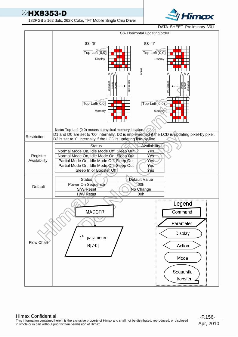
-P.156- Himax Confidential
Apr, 2010
This information contained herein is the exclusive property of Himax and shall not be distributed, reproduced, or disclosed in whole or in part without prior written permission of Himax.
HX8353-D 132RGB x 162 dots, 262K Color, TFT Mobile Single Chip Driver DATA SHEET Preliminary V01
SS- Horizontal Updating order
SS="0"
Top-Left (0,0)
Display
Top-Left( 0,0)
Memory
SS="1"
Top-Left (0,0)
Display
Top-Left( 0,0)
Memory
SentF
irst(1)
Sent2nd
SentF
irst(1)
Sent3rd
Sent3rd
Sent2nd
Sent3rd
Sentlast
(132)
Sentlast
(132)
Note: Top-Left (0,0) means a physical memory location.
Restriction D1 and D0 are set to ‘00’ internally. D2 is implemented if the LCD is updating pixel-by pixel. D2 is set to ‘0’ internally if the LCD is updating line-by-line.
Register Availability
Status Availability Normal Mode On, Idle Mode Off, Sleep Out Yes Normal Mode On, Idle Mode On, Sleep Out Yes Partial Mode On, Idle Mode Off, Sleep Out Yes Partial Mode On, Idle Mode On, Sleep Out Yes
Sleep In or Booster Off Yes
Default
Status Default Value Power On Sequence 00h
S/W Reset No Change H/W Reset 00h
Flow Chart

-P.157- Himax Confidential
Apr, 2010
This information contained herein is the exclusive property of Himax and shall not be distributed, reproduced, or disclosed in whole or in part without prior written permission of Himax.
HX8353-D 132RGB x 162 dots, 262K Color, TFT Mobile Single Chip Driver DATA SHEET Preliminary V01
8.2.30 Vertical scrolling start address (37h)
37 H VSCRSADD (Vertical Scrolling Start Address) DNC NRD NWR D15-8 D7 D6 D5 D4 D3 D2 D1 D0 HEX Command 0 1 ↑ - 0 0 1 1 0 1 1 1 37 1st parameter 1 1 ↑ - VSP 15 VSP 14 VSP 13 VSP 12 VSP 11 VSP 10 VSP 9 VSP 8 2nd parameter 1 1 ↑ - VSP 7 VSP 6 VSP 5 VSP 4 VSP 3 VSP 2 VSP 1 VSP 0
01. 3F
This command is used together with Vertical Scrolling Definition (33h). These two commands describe the scrolling area and the scrolling mode. The Vertical Scrolling Start Address command has one parameter which describes the address of the line in the Frame Memory that will be written as the first line after the last line of the Top Fixed Area on the display as illustrated below: When MADCTL B4=’0’ Example: When Top Fixed Area = Bottom Fixed Area = 00, Vertical Scrolling Area = 162 and
When MADCTL B4=1 Example: When Top Fixed Area = Bottom Fixed Area = 00, Vertical Scrolling Area = 162 and
When new Pointer position and Picture Data are sent, the result on the display will happen at the next Panel Scan to avoid tearing effect. VSP refers to the Frame Memory line Pointer.
Restriction Since the value of the Vertical Scrolling Start Address is absolute (with reference to the Frame Memory), it must not enter the fixed area (defined by Vertical Scrolling Definition (33h) – otherwise undesirable image will be displayed on the Panel.
Register Availability
Status Availability Normal Mode On, Idle Mode Off, Sleep Out Yes Normal Mode On, Idle Mode On, Sleep Out Yes Partial Mode On, Idle Mode Off, Sleep Out Yes Partial Mode On, Idle Mode On, Sleep Out Yes
Sleep In or Booster Off Yes
Default
Status Default Value Power On Sequence 00h
S/W Reset 00h H/W Reset 00h
Flow Chart See Vertical Scrolling Definition (33h) description.
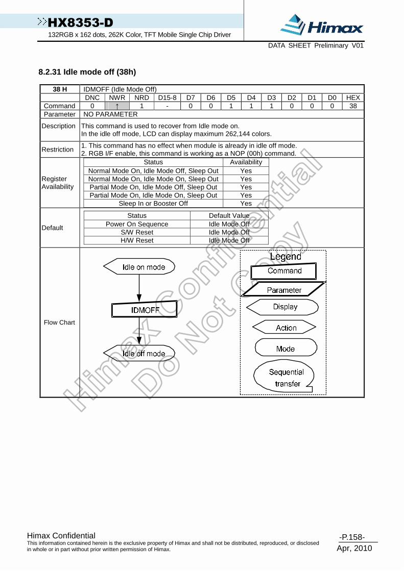
-P.158- Himax Confidential
Apr, 2010
This information contained herein is the exclusive property of Himax and shall not be distributed, reproduced, or disclosed in whole or in part without prior written permission of Himax.
HX8353-D 132RGB x 162 dots, 262K Color, TFT Mobile Single Chip Driver DATA SHEET Preliminary V01
8.2.31 Idle mode off (38h)
38 H IDMOFF (Idle Mode Off) DNC NWR NRD D15-8 D7 D6 D5 D4 D3 D2 D1 D0 HEX Command 0 ↑ 1 - 0 0 1 1 1 0 0 0 38 Parameter NO PARAMETER
Description
This command is used to recover from Idle mode on. In the idle off mode, LCD can display maximum 262,144 colors.
Restriction 1. This command has no effect when module is already in idle off mode. 2. RGB I/F enable, this command is working as a NOP (00h) command.
Register Availability
Status Availability Normal Mode On, Idle Mode Off, Sleep Out Yes Normal Mode On, Idle Mode On, Sleep Out Yes Partial Mode On, Idle Mode Off, Sleep Out Yes Partial Mode On, Idle Mode On, Sleep Out Yes
Sleep In or Booster Off Yes
Default
Status Default Value Power On Sequence Idle Mode Off
S/W Reset Idle Mode Off H/W Reset Idle Mode Off
Flow Chart

-P.159- Himax Confidential
Apr, 2010
This information contained herein is the exclusive property of Himax and shall not be distributed, reproduced, or disclosed in whole or in part without prior written permission of Himax.
HX8353-D 132RGB x 162 dots, 262K Color, TFT Mobile Single Chip Driver DATA SHEET Preliminary V01
8.2.32 Idle mode on (39h)
39 H IDMON (Idle Mode On) DNC NWR NRD D15-8 D7 D6 D5 D4 D3 D2 D1 D0 HEX Command 0 ↑ 1 - 0 0 1 1 1 0 0 1 39 Parameter NO PARAMETER
Description
This command is used to enter into Idle mode on. In the idle on mode, color expression is reduced. The primary and the secondary colors using MSB of each R, G and B in the Frame Memory, 8 color depth data is displayed.
Memory contents vs. Display Color R5 R4 R3 R2 R1 R0 G5 G4 G3 G2 G1 G0 B5 B4 B3 B2 B1 B0 Black 0XXXXX 0XXXXX 0XXXXX Blue 0XXXXX 0XXXXX 1XXXXX Red 1XXXXX 0XXXXX 0XXXXX Magenta 1XXXXX 0XXXXX 1XXXXX Green 0XXXXX 1XXXXX 0XXXXX Cyan 0XXXXX 1XXXXX 1XXXXX Yellow 1XXXXX 1XXXXX 0XXXXX White 1XXXXX 1XXXXX 1XXXXX
Restriction This command has no effect when module is already in idle off mode.
Register Availability
Status Availability Normal Mode On, Idle Mode Off, Sleep Out Yes Normal Mode On, Idle Mode On, Sleep Out Yes Partial Mode On, Idle Mode Off, Sleep Out Yes Partial Mode On, Idle Mode On, Sleep Out Yes
Sleep In or Booster Off Yes
Default
Status Default Value Power On Sequence Idle Mode Off
S/W Reset Idle Mode Off H/W Reset Idle Mode Off

-P.160- Himax Confidential
Apr, 2010
This information contained herein is the exclusive property of Himax and shall not be distributed, reproduced, or disclosed in whole or in part without prior written permission of Himax.
HX8353-D 132RGB x 162 dots, 262K Color, TFT Mobile Single Chip Driver DATA SHEET Preliminary V01
Flow Chart

-P.161- Himax Confidential
Apr, 2010
This information contained herein is the exclusive property of Himax and shall not be distributed, reproduced, or disclosed in whole or in part without prior written permission of Himax.
HX8353-D 132RGB x 162 dots, 262K Color, TFT Mobile Single Chip Driver DATA SHEET Preliminary V01
8.2.33 Interface pixel format (3Ah)
3A H COLMOD (Interface Pixel Format) DNC NWR NRD D15-8 D7 D6 D5 D4 D3 D2 D1 D0 HEX Command 0 ↑ 1 - 0 0 1 1 1 0 1 0 3A
1st parameter 1 ↑ 1 - - - - - - D2 D1 D0 011, 101, 110
Description
This command is used to define the format of RGB picture data, which is to be transfer via the system interface. The formats are shown in the table:
Interface Format D2 D1 D0 Not Defined 0 0 0 Not Defined 0 0 1 Not Defined 0 1 0 12 Bit/Pixel 0 1 1 Not Defined 1 0 0 16 Bit/Pixel 1 0 1 18 Bit/Pixel 1 1 0 Not Defined 1 1 1
Restriction -
Register Availability
Status Availability Normal Mode On, Idle Mode Off, Sleep Out Yes Normal Mode On, Idle Mode On, Sleep Out Yes Partial Mode On, Idle Mode Off, Sleep Out Yes Partial Mode On, Idle Mode On, Sleep Out Yes
Sleep In or Booster Off Yes
Default
Status Default Value Power On Sequence 18-bit/pixel
S/W Reset No Change H/W Reset 18-bit/pixel
Flow Chart

-P.162- Himax Confidential
Apr, 2010
This information contained herein is the exclusive property of Himax and shall not be distributed, reproduced, or disclosed in whole or in part without prior written permission of Himax.
HX8353-D 132RGB x 162 dots, 262K Color, TFT Mobile Single Chip Driver DATA SHEET Preliminary V01
8.2.34 Read ID1 (DAh) DA H RDID1 (Read ID1) DNC NWR NRD D15-8 D7 D6 D5 D4 D3 D2 D1 D0 HEX Command 0 ↑ 1 - 1 1 0 1 1 0 1 0 DA 1st parameter 1 1 ↑ - - - - - - - - - -
2nd parameter 1 1 ↑ - module’s manufacturer m[7:0] -
Description This read byte identifies the LCD module’s manufacturer.
Restriction -
Register Availability
Status Availability Normal Mode On, Idle Mode Off, Sleep Out Yes Normal Mode On, Idle Mode On, Sleep Out Yes Partial Mode On, Idle Mode Off, Sleep Out Yes Partial Mode On, Idle Mode On, Sleep Out Yes
Sleep In or Booster Off Yes
Default
Status Default Value Power On Sequence xxHEX
S/W Reset xxHEX H/W Reset xxHEX
Flow Chart

-P.163- Himax Confidential
Apr, 2010
This information contained herein is the exclusive property of Himax and shall not be distributed, reproduced, or disclosed in whole or in part without prior written permission of Himax.
HX8353-D 132RGB x 162 dots, 262K Color, TFT Mobile Single Chip Driver DATA SHEET Preliminary V01
8.2.35 Read ID2 (DBh) DB H RDID2 (Read ID2) DNC NWR NRD D15-8 D7 D6 D5 D4 D3 D2 D1 D0 HEX Command 0 ↑ 1 - 1 1 0 1 1 0 1 1 DB
1st parameter 1 1 ↑ - - - - - - - - - - 2nd parameter 1 1 ↑ - 1 V6 V5 V4 V3 V2 V1 V0 -
Description
This read byte is used to track the LCD module/driver version. It is defined by display supplier and changes each time a revision is made to the display, material or construction specifications. See the following table.
ID Byte Value V[7:0]
Version Changes
80h - - 81h - - 82h - - 83h - - 84h - - 85h - -
Restrictions
Register Availability
Status Availability Normal Mode On, Idle Mode Off, Sleep Out Yes Normal Mode On, Idle Mode On, Sleep Out Yes Partial Mode On, Idle Mode Off, Sleep Out Yes Partial Mode On, Idle Mode On, Sleep Out Yes Sleep In or Booster Off Yes
Default
Status Default Value Power On Sequence See Description
S/W Reset See Description H/W Reset See Description
Flow Chart

-P.164- Himax Confidential
Apr, 2010
This information contained herein is the exclusive property of Himax and shall not be distributed, reproduced, or disclosed in whole or in part without prior written permission of Himax.
HX8353-D 132RGB x 162 dots, 262K Color, TFT Mobile Single Chip Driver DATA SHEET Preliminary V01
8.2.36 Read ID3 (DCh)
DC H RDID3 (Read ID3)
DNC
NWR NRD D15-8 D7 D6 D5 D4 D3 D2 D1 D0 HEX
Command 0 ↑ 1 - 1 1 0 1 1 1 0 0 DC 1st parameter 1 1 ↑ - - - - - - - - - - 2nd parameter 1 1 ↑ - ID7 ID6 ID5 ID4 ID3 ID2 ID1 ID0 -
Description This read byte identifies the LCD module/driver.
Restrictions
Register Availability
Status Availability Normal Mode On, Idle Mode Off, Sleep Out Yes Normal Mode On, Idle Mode On, Sleep Out Yes Partial Mode On, Idle Mode Off, Sleep Out Yes Partial Mode On, Idle Mode On, Sleep Out Yes Sleep In or Booster Off Yes
Default
Status Default Value Power On Sequence xxHEX
S/W Reset xxHEX H/W Reset xxHEX
Flow Chart
Legend
Command
Parameter
Display
Action
Mode
Sequential
transfer
Serial I/F Mode
Read ID3
Send ID[7:0]
Host
Display
Parallel I/F Mode
Read ID3
Dummy read
Send ID[7:0]

-P.165- Himax Confidential
Apr, 2010
This information contained herein is the exclusive property of Himax and shall not be distributed, reproduced, or disclosed in whole or in part without prior written permission of Himax.
HX8353-D 132RGB x 162 dots, 262K Color, TFT Mobile Single Chip Driver DATA SHEET Preliminary V01
8.2.37 SETOSC: set internal oscillator (B0h)
B0 H SETOSC( Set Internal Oscillator) DNC NWR NRD D17-8 D7 D6 D5 D4 D3 D2 D1 D0 HEX Command 0 ↑ 1 - 1 0 1 1 0 0 0 0 B0 1st parameter
1 ↑ 1 - I_RADJ[1:0] N_RADJ[1:0] C4
2nd parameter
1 ↑ 1 - - - - - - - - OSC_EN 00
Description
These command is used to set internal oscillator related setting OSC_EN: Enable internal oscillator, OSC_EN = ‘1’, internal oscillator start to oscillate. OSC_EN = ‘0’, internal oscillator stop. N_RADJ[1:0]: Internal oscillator frequency adjusts in Normal / Partial mode. I_RADJ[1:0]: Internal oscillator frequency adjusts in Idle(8-color) / Partial Idle mode. For details, please refer to “7.1 Internal Oscillator” section.
RADJ1 RADJ0 Internal Oscillator
Frequency 0 0 147.4% 0 1 127.1% 1 0 111.7% 1 1 100%
Restrictions If EXTC is high or enable SETEXTC command (even EXTC = low) can enable this command
Register Availability
Status Availability Normal Mode On, Idle Mode Off, Sleep Out Yes Normal Mode On, Idle Mode On, Sleep Out Yes Partial Mode On, Idle Mode Off, Sleep Out Yes Partial Mode On, Idle Mode On, Sleep Out Yes
Sleep In or Booster Off Yes
Default
Status Default Value Power On Sequence I_RADJ[1:0]=11, N_RADJ[1:0]=10, OSC_EN=0
S/W Reset OSC_EN=0, others no change H/W Reset I_RADJ[1:0]=11, N_RADJ[1:0]=10, OSC_EN=0
Flow Chart -

-P.166- Himax Confidential
Apr, 2010
This information contained herein is the exclusive property of Himax and shall not be distributed, reproduced, or disclosed in whole or in part without prior written permission of Himax.
HX8353-D 132RGB x 162 dots, 262K Color, TFT Mobile Single Chip Driver DATA SHEET Preliminary V01
8.2.38 SETPOWER: set power (B1h)
B1 H SETPOWER (Set Power )
DNC NWR NRD D17-8 D7 D6 D5 D4 D3 D2 D1 D0 HEX
Command 0 ↑ 1 - 1 0 1 1 0 0 0 1 B1
1st parameter 1 ↑ 1 - - - - - - - DP_STB
DP_STB_S
00
2nd parameter 1 ↑ 1 - - - - - - BT[2:0] 01 3rd parameter 1 ↑ 1 - - - VRH[5:0] 1B 4th parameter 1 ↑ 1 - - - - - - AP[2:0] 03 5th parameter 1 ↑ 1 - FS0[7:0] 04 6th parameter 1 ↑ 1 - FS1[7:0] 04 7th parameter 1 ↑ 1 - - - - - - - - - 11 8th parameter 1 ↑ 1 - GASEN VCOMG - PON DK - - STB 89
Description
DP_STB, DP_STB_S : These two bits can let the driver into the deep standby mode. And when into deep standby, all display operation stops, including the internal R-C oscillator. In the deep standby mode, the GRAM data and register content are not retained. VRH[5:0]: Specify the VREG1 voltage adjusting. VREG1 voltage is for gamma voltage
setting.VREG1=Decimal(VRH[5:0])x0.05+3.3.
VRH5 VRH4 VRH3 VRH2 VRH1 VRH0 VREG1
0 0 0 0 0 0 3.30 0 0 0 0 0 1 3.35 0 0 0 0 1 0 3.40 0 0 0 0 1 1 3.45 0 0 0 1 0 0 3.50 0 0 0 1 0 1 3.55
: : : : : : : 0 1 1 1 0 1 4.75 0 1 1 1 1 0 4.80 0 1 1 1 1 1 STOP 1 0 0 0 0 0 STOP
: : : : : : : 1 1 0 0 0 0 STOP 1 1 0 0 0 1 STOP 1 1 0 0 1 0 STOP 1 1 0 0 1 1 STOP
: : : : : : : 1 1 1 1 1 0 STOP
1 1 1 1 1 1
Internal circuit operations stop. The gamma voltage can be adjusted from external VREG1 input.
Note: (1) Internal reference voltage VREF=4.8V ( Please set DDVDH_TRI=0) (2) Internal VREF can be modified by Custom’s special request.
VREG1=Decimal(VRH[5:0])x0.05+3.3 *(VREF/4.8) ( Please set DDVDH_TRI=0)

-P.167- Himax Confidential
Apr, 2010
This information contained herein is the exclusive property of Himax and shall not be distributed, reproduced, or disclosed in whole or in part without prior written permission of Himax.
HX8353-D 132RGB x 162 dots, 262K Color, TFT Mobile Single Chip Driver DATA SHEET Preliminary V01
BT[2:0]: Switch the output factor of step-up circuit 2 for VGH and VGL voltage generation.
The LCD drive voltage level can be selected according to the characteristic of liquid crystal which panel used. Lower amplification of the step-up circuit consumes less current and then the power consumption can be reduced.
BT2 BT1 BT0 DDVDH VCL VGH VGL
0 0 0 5.0V -VCI 11V ~ 14.5V -8V ~ -12.5V
0 0 1 5.0V -VCI 11V ~ 14.5V -6V ~ -10V
0 1 0 5.0V -VCI 11V ~ 14.5V -5V ~ -7V
0 1 1 5.0V -VCI 9V ~ 12.5V -8V ~ -12.5V
1 0 0 5.0V -VCI 9V ~ 12.5V -6V ~ -10V
1 0 1 5.0V -VCI 9V ~ 12.5V -5V ~ -7V
1 1 0 5.0V -VCI 8V ~ 10V -6V ~ -10V
1 1 1 5.0V -VCI 8V ~ 10V -5V ~ -7V
Note1: When VCI = 2.8V and DDVDH_TRI=0 Note2: The “VGH” & “VGL” value depend on panel Note3: The VGH v.s Ivgh and VGL v.s. Ivgl ,please reference the chapter 11.3 DC characteristic
AP[2:0]: Adjust the amount of current driving for the operational amplifier in the power supply circuit. When the amount of fixed current is increased, the LCD driving capacity and the display quality are high, but the current consumption is increased. Adjust the fixed current by considering both the display quality and the current consumption.
AP2 AP1 AP0 Constant Current of Operational Amplifier 0 0 0 Operation of the operational amplifier stops 0 0 1 Small 0 1 0 Small 0 1 1 Small 1 0 0 Medium 1 0 1 Medium High 1 1 0 Large 1 1 1 Small

-P.168- Himax Confidential
Apr, 2010
This information contained herein is the exclusive property of Himax and shall not be distributed, reproduced, or disclosed in whole or in part without prior written permission of Himax.
HX8353-D 132RGB x 162 dots, 262K Color, TFT Mobile Single Chip Driver DATA SHEET Preliminary V01
FS0[7:0]: Set the operating frequency for DDVDH and VCL voltage generation. For details, please refer to “7.1 Internal Oscillator” section.
FS07 FS06 FS05 FS04 FS03 FS02 FS01 FS00 Operation Frequency for DDVDH and VCL
0 0 0 0 0 0 0 0 TIMING_CLK/2 0 0 0 0 0 0 0 1 TIMING_CLK/2 0 0 0 0 0 0 1 0 TIMING_CLK/4 0 0 0 0 0 0 1 1 TIMING_CLK/6 0 0 0 0 0 1 0 0 TIMING_CLK/8 0 0 0 0 0 1 0 1 TIMING_CLK/10 : : : : : : : : : 1 1 1 1 1 1 1 0 TIMING_CLK/508 1 1 1 1 1 1 1 1 TIMING_CLK/510
Note : TIMING_CLK = TIMING_CLK/(2*X) ; X = FS0’s Value. FS1[7:0]: Set the operating frequency for VGH and VGL voltage generation. For details, please refer to “7.1 Internal Oscillator” section.
FS17 FS16 FS15 FS14 FS13 FS12 FS11 FS10 Operation Frequency
for VGH and VGL 0 0 0 0 0 0 0 0 TIMING_CLK/1 0 0 0 0 0 0 0 1 TIMING_CLK/1 0 0 0 0 0 0 1 0 TIMING_CLK/2 0 0 0 0 0 0 1 1 TIMING_CLK/3 : : : : : : : : : 1 1 1 1 1 1 0 1 TIMING_CLK/253 1 1 1 1 1 1 1 0 TIMING_CLK/254 1 1 1 1 1 1 1 1 TIMING_CLK/255
Note: TIMING_CLK = TIMING_CLK/X ; X = FS1’s Value. Ensure that the operation frequency of FS0 ≧ FS1.
STB: When STB = “1”, the HX8353-D into the standby mode, where all display operation stops, suspend all the internal operations including the internal R-C oscillator. During the standby mode, only the following process can be executed.
a. Exit the Standby mode (STB = “0”) , b. Start the oscillation
In the standby mode, the GRAM data and register content will be keeping. GASEN: This stands for abnormal power-off monitor function when the power is off. DK: Specify on/off control of step-up circuit 1 for DDVDH voltage generation. For detail, see the Power Supply Setting Sequence.
DK Operation of step-up circuit 1
0 ON
1 OFF PON: Specify on/off control of step-up circuit 2 for VCL, VGL voltage generation. For detail, see the Power Supply Setting Sequence.
PON Operation of step-up circuit 2 0 OFF 1 ON
VCOMG: When VCOMG = ‘1’, VCOML voltage can output to negative voltage. When

-P.169- Himax Confidential
Apr, 2010
This information contained herein is the exclusive property of Himax and shall not be distributed, reproduced, or disclosed in whole or in part without prior written permission of Himax.
HX8353-D 132RGB x 162 dots, 262K Color, TFT Mobile Single Chip Driver DATA SHEET Preliminary V01
VCOMG = ‘0’, VCOML = GND. DK: set “0” => DDVDH Enable, set “1” => DDVDH Disable.
Restrictions If EXTC is high or enable SETEXTC command (even EXTC = low) can enable this command
Register Availability
Status Availability
Normal Mode On, Idle Mode Off, Sleep Out Yes Normal Mode On, Idle Mode On, Sleep Out Yes Partial Mode On, Idle Mode Off, Sleep Out Yes Partial Mode On, Idle Mode On, Sleep Out Yes
Sleep In or Booster Off Yes
Default
Status Default Value
Power On Sequence
DP_STB=0, DP_STB_S=0, BT[2:0]=3’b011, VRH[5:0]=6’b011011, AP[2:0]=3’b011, FS0[7:0]=8’h01, FS1[7:0]=8’h10, BLANK_FS0[3:0]=4’b0001, BLANK_FS1[3:0]= 4’b0001, GASEN=1, VCOMG=0, PON=0, DK=1, STB=1
S/W Reset VCOMG=0, PON=0, DK=1, STB=1, others no change
H/W Reset
DP_STB=0, DP_STB_S=0, BT[2:0]=3’b011, VRH[5:0]=6’b011011, AP[2:0]=3’b011, FS0[7:0]=8’h01, FS1[7:0]=8’h10, BLANK_FS0[3:0]=4’b0001, BLANK_FS1[3:0]= 4’b0001, GASEN=1, VCOMG=0, PON=0, DK=1, STB=1
Flow Chart -

-P.170- Himax Confidential
Apr, 2010
This information contained herein is the exclusive property of Himax and shall not be distributed, reproduced, or disclosed in whole or in part without prior written permission of Himax.
HX8353-D 132RGB x 162 dots, 262K Color, TFT Mobile Single Chip Driver DATA SHEET Preliminary V01
8.2.39 SETDISPLAY: set display related register (B2 h)
B2H SETDISPLAY( Set Display Control ) DNC NWR NRD D17-8 D7 D6 D5 D4 D3 D2 D1 D0 HEX Command 0 ↑ 1 - 1 0 1 1 0 0 1 0 B2 1st parameter 1 ↑ 1 - - - - - ISC[3:0] 01 2nd parameter 1 ↑ 1 - PT[1:0] PTV[1:0] - - PTG REF 93 3rd parameter 1 ↑ 1 - - - GON DTE D1 D0 - - 20
This command is used to set display related register D[1:0]: When D1 = ‘1’, display is on; when D1 = ‘0’, display is off. When display is off, the display data is retained in the GRAM and the entire source outputs are set to the VSSD level. When D[1:0]= ‘01’, the internal display of the HX8353-D is performed although the actual display is off. When D[1:0]= ‘00’, the internal display operation halts and the display is off.
D1 D0 Source Output Internal Display Operations Gate-Driver Control Signals 0 0 VSSD Halt Halt 0 1 VSSD Operate Operate 1 0 =PT(0,0) Operate Operate 1 1 Display Operate Operate
GON, DTE:
GON DTE Gate Output 1 0 Fixed to VGL 1 1 Normal Operation
(VGH/VGL) PT[1:0] : Specify the Non-display area source output in partial display mode.
Source Output Level
Non-display Area Display area
PT1-0=(0,*) PT1-0=(1,0) PT1-0=(1,1) REV_Panel GRAM Data
VCOM = “L”
VCOM = “H”
VCOM = “L”
VCOM = “H”
VCOM = “L”
VCOM = “H”
VCOM = “L”
VCOM = “H”
1 (Normally
Black Panel)
18’h00000 :
18’h3FFFF
V63P :
V0P
V0N :
V63N V63P V0N GND GND Hi-z Hi-z
0 (Normally
White Panel)
18’h00000 :
18’h3FFFF
V0P :
V63P
V63N :
V0N V63P V0N GND GND Hi-z Hi-z
Description
REF: Refresh display in non-display area in Partial mode enable bit. REF = ‘0’: Refresh display operation is disabling. REF = ‘1’: Refresh display operation is enable.
PTG: Specify the scan mode of gate driver in non-display area.
PTG Gate Outputs in Non-display Area
0 Normal Drive 1 Fixed VGL
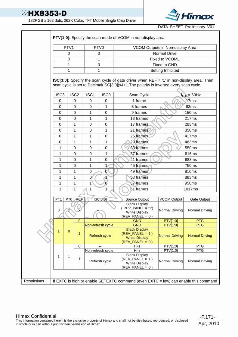
-P.171- Himax Confidential
Apr, 2010
This information contained herein is the exclusive property of Himax and shall not be distributed, reproduced, or disclosed in whole or in part without prior written permission of Himax.
HX8353-D 132RGB x 162 dots, 262K Color, TFT Mobile Single Chip Driver DATA SHEET Preliminary V01
PTV[1:0]: Specify the scan mode of VCOM in non-display area.
PTV1 PTV0 VCOM Outputs in Non-display Area
0 0 Normal Drive 0 1 Fixed to VCOML 1 0 Fixed to GND 1 1 Setting Inhibited
ISC[3:0]: Specify the scan cycle of gate driver when REF = ‘1’ in non-display area. Then scan cycle is set to Decimal(ISC[3:0])x4+1.The polarity is inverted every scan cycle.
ISC3 ISC2 ISC1 ISC0 Scan Cycle fFLM = 60Hz
0 0 0 0 1 frame 17ms
0 0 0 1 5 frames 83ms
0 0 1 0 9 frames 150ms
0 0 1 1 13 frames 217ms
0 1 0 0 17 frames 283ms
0 1 0 1 21 frames 350ms
0 1 1 0 25 frames 417ms
0 1 1 1 29 frames 483ms
1 0 0 0 33 frames 550ms
1 0 0 1 37 frames 616ms
1 0 1 0 41 frames 683ms
1 0 1 1 45 frames 750ms
1 1 0 0 49 frames 816ms
1 1 0 1 53 frames 883ms
1 1 1 0 57 frames 950ms
1 1 1 1 61 frames 1017ms
PT1 PT0 REF ISC[3:0] Source Output VCOM Output Gate Output
0 x x --
Black Display ( REV_PANEL = ‘1’)
White Display (REV_PANEL = ‘0’)
Normal Driving Normal Driving
0 -- GND PTV[1:0] PTG Non-refresh cycle GND PTV[1:0] PTG
1 0 1
Refresh cycle
Black Display (REV_PANEL = ‘1’)
White Display (REV_PANEL = ‘0’)
Normal Driving Normal Driving
0 -- Hi-z PTV[1:0] PTG Non-refresh cycle Hi-z PTV[1:0] PTG
1 1 1
Refresh cycle
Black Display (REV_PANEL = ‘1’)
White Display (REV_PANEL = ‘0’)
Normal Driving Normal Driving
Restrictions If EXTC is high or enable SETEXTC command (even EXTC = low) can enable this command

-P.172- Himax Confidential
Apr, 2010
This information contained herein is the exclusive property of Himax and shall not be distributed, reproduced, or disclosed in whole or in part without prior written permission of Himax.
HX8353-D 132RGB x 162 dots, 262K Color, TFT Mobile Single Chip Driver DATA SHEET Preliminary V01
Register Availability
Status Availability Normal Mode On, Idle Mode Off, Sleep Out Yes Normal Mode On, Idle Mode On, Sleep Out Yes Partial Mode On, Idle Mode Off, Sleep Out Yes Partial Mode On, Idle Mode On, Sleep Out Yes
Sleep In or Booster Off Yes
Default
Status Default Value
Power On Sequence ISC[3:0]=4’b0001, PT[1:0]=2’b10, PTV[1:0]=2’b01, PTG=1, REF=1, GON=1, DTE=0, D[1:0]=2’b00
S/W Reset GON=1, D0=0, others no change
H/W Reset ISC[3:0]=4’b0001, PT[1:0]=2’b10, PTV[1:0]=2’b10, PTG=1, REF=1, GON=1, DTE=0, D[1:0]=2’b00
Flow Chart -

-P.173- Himax Confidential
Apr, 2010
This information contained herein is the exclusive property of Himax and shall not be distributed, reproduced, or disclosed in whole or in part without prior written permission of Himax.
HX8353-D 132RGB x 162 dots, 262K Color, TFT Mobile Single Chip Driver DATA SHEET Preliminary V01
8.2.40 SETCYC: set display cycle register (B4h)
B4 H SETCYC ( Set display cycle ) DNC NWR NRD D17-8 D7 D6 D5 D4 D3 D2 D1 D0 HEX Command 0 ↑ 1 - 1 0 1 1 0 1 0 0 B4 1st parameter 1 ↑ 1 - - I/_NW[2:0] - N_NW[2:0] 01 2nd parameter 1 ↑ 1 - I_RTN[3:0] N_RTN[3:0] 04 3rd parameter 1 ↑ 1 - I_DIV[3:0] N_DIV[3:0] FF 4th parameter 1 ↑ 1 - N_DUM[7:0] 0C 5th parameter 1 ↑ 1 - I_DUM[7:0] 0C 6th parameter 1 ↑ 1 - GDON[7:0] 0D 7th parameter 1 ↑ 1 - GDOF[7:0] 53 8th parameter 1 ↑ 1 - L_BASE[7:0] 59
This command is used to set display related register N_ NW[2:0]: Specify LCD driving inversion type in Normal/ Partial mode. I_ NW[2:0]: Specify LCD driving inversion type in Idle / Partial Idle mode.
NW[2:0] LCD driving Inversion Type
0d Frame inversion 1d 1-line inversion 2d 2-line inversion 3d 3-line inversion : :
6d 6-line inversion 7d 7-line inversion
N_DIV[3:0]: Specify the division ratio of internal clocks in Normal / Partial mode for internal operation. When used internal clock for the display operation, frame frequency can be adjusted with the N_RTN[3:0] bits (1H period clock cycle), N_DIV[3:0], and N_DUM[7:0] bits. I_DIV[3:0]: Specify the division ratio of internal clocks in Idle (8-color) / Partial Idle mode for internal operation. When used internal clock for the display operation, frame frequency can be adjusted with the I_RTN[3:0] bits(1H period clock cycle), I_DIV[3:0], and I_DUM[7:0] bits.
fosc = R-C oscillation frequency
DIV3 DIV2 DIV1 DIV0 Division
Ratio Internal Display Operation
Clock Frequency 0 0 0 0 1 fosc / 1 0 0 0 1 1 fosc / 1 0 0 1 0 1.5 fosc / 1.5 0 0 1 1 2 fosc / 2 0 1 0 0 2.5 fosc / 2.5 0 1 0 1 3 fosc / 3 0 1 1 0 3.5 fosc / 3.5 : : : : : : 1 1 0 1 7 fosc / 7 1 1 1 0 7.5 fosc / 7.5 1 1 1 1 1.5 fosc / 1.5 (defaule)
Description
N_RTN[3:0]: Specify clock number of one line period in Normal / Partial mode for internal operation.

-P.174- Himax Confidential
Apr, 2010
This information contained herein is the exclusive property of Himax and shall not be distributed, reproduced, or disclosed in whole or in part without prior written permission of Himax.
HX8353-D 132RGB x 162 dots, 262K Color, TFT Mobile Single Chip Driver DATA SHEET Preliminary V01
I_ RTN[3:0]: Specify clock number of one line period in Idle (8-color) / Partial Idle mode for internal operation.
Clock cycles=1/internal operation clock frequency(fosc)
RTN[3:0] Clock number per Line 4’b0000 89 4’b0001 90 4’b0010 91 4’b0011 92 4’b0100 93
: : 4’b1110 103 4’b1111 104
N_DUM[7:0]: Specify dummy line number in blanking area of one frame in Normal / Partial
mode for internal operation. I_DUM[7:0]: Specify dummy line number in blanking area of one frame in Idle (8-color) /
Partial Idle mode for internal operation.
DUM[7:0] Line number in blanking period
000d Setting Inhibited 001d Setting Inhibited 002d 2 003d 3 004d 4
: : 190d 190
others Setting Inhibited Formula for the Frame Frequency during internal display mode: Frame frequency = fosc/( RTN × DIV × (162+DUM) ) [Hz] fosc: RC oscillation frequency GDON[7:0]: Specify the valid gate output start time in 1-line driving period. The period
time value is defined as SYSCLK number in internal clock display mode. The period time value is defined as DOTCLK number in 18/16-bit bus width RGB display mode and is defined as DOTCLK/3 number in 6-bit bus width RGB display mode. (Please note that the setting “00h”, “01h”, “02h” is inhibited).
GDOF[7:0]: Specify the gate output end time in 1-line driving period. The period time value
is defined as SYSCLK number in internal clock display mode. The period time value is defined as DOTCLK number in 18/16-bit bus width RGB display mode and is defined as DOTCLK/3 number in 6-bit bus width RGB display mode. (Please note that the GDON[7:0] + 1≤ GDOF[7:0] ≤ RTN-1).
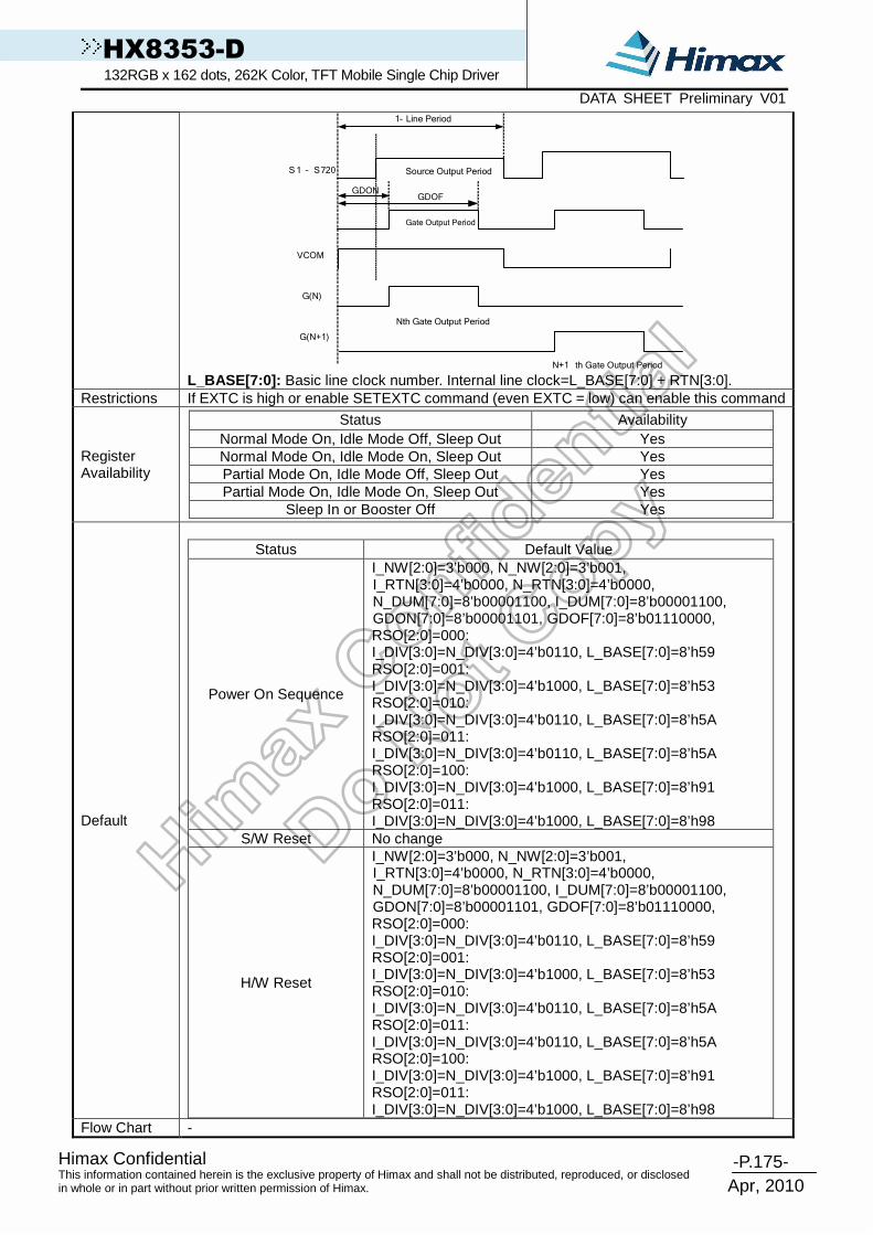
-P.175- Himax Confidential
Apr, 2010
This information contained herein is the exclusive property of Himax and shall not be distributed, reproduced, or disclosed in whole or in part without prior written permission of Himax.
HX8353-D 132RGB x 162 dots, 262K Color, TFT Mobile Single Chip Driver DATA SHEET Preliminary V01
1- Line Period
GDONGDOF
Source Output Period
Gate Output Period
Nth Gate Output Period
N+1 th Gate Output Period
S1 – S720
G(N)
G(N+1)
VCOM
L_BASE[7:0]: Basic line clock number. Internal line clock=L_BASE[7:0] + RTN[3:0].
Restrictions If EXTC is high or enable SETEXTC command (even EXTC = low) can enable this command
Register Availability
Status Availability Normal Mode On, Idle Mode Off, Sleep Out Yes Normal Mode On, Idle Mode On, Sleep Out Yes Partial Mode On, Idle Mode Off, Sleep Out Yes Partial Mode On, Idle Mode On, Sleep Out Yes
Sleep In or Booster Off Yes
Default
Status Default Value
Power On Sequence
I_NW[2:0]=3’b000, N_NW[2:0]=3’b001, I_RTN[3:0]=4’b0000, N_RTN[3:0]=4’b0000, N_DUM[7:0]=8’b00001100, I_DUM[7:0]=8’b00001100, GDON[7:0]=8’b00001101, GDOF[7:0]=8’b01110000, RSO[2:0]=000: I_DIV[3:0]=N_DIV[3:0]=4’b0110, L_BASE[7:0]=8’h59 RSO[2:0]=001: I_DIV[3:0]=N_DIV[3:0]=4’b1000, L_BASE[7:0]=8’h53 RSO[2:0]=010: I_DIV[3:0]=N_DIV[3:0]=4’b0110, L_BASE[7:0]=8’h5A RSO[2:0]=011: I_DIV[3:0]=N_DIV[3:0]=4’b0110, L_BASE[7:0]=8’h5A RSO[2:0]=100: I_DIV[3:0]=N_DIV[3:0]=4’b1000, L_BASE[7:0]=8’h91 RSO[2:0]=011: I_DIV[3:0]=N_DIV[3:0]=4’b1000, L_BASE[7:0]=8’h98
S/W Reset No change
H/W Reset
I_NW[2:0]=3’b000, N_NW[2:0]=3’b001, I_RTN[3:0]=4’b0000, N_RTN[3:0]=4’b0000, N_DUM[7:0]=8’b00001100, I_DUM[7:0]=8’b00001100, GDON[7:0]=8’b00001101, GDOF[7:0]=8’b01110000, RSO[2:0]=000: I_DIV[3:0]=N_DIV[3:0]=4’b0110, L_BASE[7:0]=8’h59 RSO[2:0]=001: I_DIV[3:0]=N_DIV[3:0]=4’b1000, L_BASE[7:0]=8’h53 RSO[2:0]=010: I_DIV[3:0]=N_DIV[3:0]=4’b0110, L_BASE[7:0]=8’h5A RSO[2:0]=011: I_DIV[3:0]=N_DIV[3:0]=4’b0110, L_BASE[7:0]=8’h5A RSO[2:0]=100: I_DIV[3:0]=N_DIV[3:0]=4’b1000, L_BASE[7:0]=8’h91 RSO[2:0]=011: I_DIV[3:0]=N_DIV[3:0]=4’b1000, L_BASE[7:0]=8’h98
Flow Chart -

-P.176- Himax Confidential
Apr, 2010
This information contained herein is the exclusive property of Himax and shall not be distributed, reproduced, or disclosed in whole or in part without prior written permission of Himax.
HX8353-D 132RGB x 162 dots, 262K Color, TFT Mobile Single Chip Driver DATA SHEET Preliminary V01
8.2.41 SETBGP: set BGP voltage related register (B5 h)
B5 H SETBGP( Set VBGP Voltage) DNC NWR NRD D17-8 D7 D6 D5 D4 D3 D2 D1 D0 HEX
Command 0 ↑ 1 - 1 0 1 1 0 1 0 1 B5
1st parameter 1 ↑ 1 - FBOFF - - DDVDH_TRI VVDHS_SEL[3:0] 0B
2nd parameter 1 ↑ 1 - - - - - VREF[3:0] 0B 3rd parameter 1 ↑ 1 - - - - - VR_TRIM[3:0] 07
Description
The DDVDH setting table:
DDVDH_TRI=0 Set VREF @
VVDHS_SEL[3:0] DDVDH
0 0 0 0 4.068
0 0 0 1 4.176
0 0 1 0 4.284
0 0 1 1 4.392
0 1 0 0 4.5
0 1 0 1 4.608
0 1 1 0 4.716
0 1 1 1 4.824
1 0 0 0 4.932
1 0 0 1 5.04
1 0 1 0 5.148
1 0 1 1 5.256
1 1 0 0 5.364
1 1 0 1 5.472
1 1 1 0 5.58
1.8 V
1 1 1 1 5.688 The VREF setting table:
DDVDH_TRI=0
VREF[3:0] VREF
0 0 0 0 4.1
0 0 0 1 4.2
0 0 1 0 4.3
0 0 1 1 4.4
0 1 0 0 4.45
0 1 0 1 4.5
0 1 1 0 4.55
0 1 1 1 4.6
1 0 0 0 4.65
1 0 0 1 4.7
1 0 1 0 4.75
1 0 1 1 4.8
1 1 0 0 4.85
1 1 0 1 4.9
1 1 1 0 4.95
1 1 1 1 5
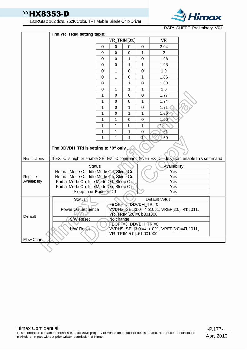
-P.177- Himax Confidential
Apr, 2010
This information contained herein is the exclusive property of Himax and shall not be distributed, reproduced, or disclosed in whole or in part without prior written permission of Himax.
HX8353-D 132RGB x 162 dots, 262K Color, TFT Mobile Single Chip Driver DATA SHEET Preliminary V01
The VR_TRIM setting table: VR_TRIM[3:0] VR
0 0 0 0 2.04
0 0 0 1 2
0 0 1 0 1.96
0 0 1 1 1.93
0 1 0 0 1.9
0 1 0 1 1.86
0 1 1 0 1.83
0 1 1 1 1.8
1 0 0 0 1.77
1 0 0 1 1.74
1 0 1 0 1.71
1 0 1 1 1.69
1 1 0 0 1.66
1 1 0 1 1.64
1 1 1 0 1.61
1 1 1 1 1.59 The DDVDH_TRI is setting to “0“ only .
Restrictions If EXTC is high or enable SETEXTC command (even EXTC = low) can enable this command
Register Availability
Status Availability Normal Mode On, Idle Mode Off, Sleep Out Yes Normal Mode On, Idle Mode On, Sleep Out Yes Partial Mode On, Idle Mode Off, Sleep Out Yes Partial Mode On, Idle Mode On, Sleep Out Yes
Sleep In or Booster Off Yes
Default
Status Default Value
Power On Sequence FBOFF=0, DDVDH_TRI=0, VVDHS_SEL[3:0]=4’b1001, VREF[3:0]=4’b1011, VR_TRIM[5:0]=6’b001000
S/W Reset No change
H/W Reset FBOFF=0, DDVDH_TRI=0, VVDHS_SEL[3:0]=4’b1001, VREF[3:0]=4’b1011, VR_TRIM[5:0]=6’b001000
Flow Chart -

-P.178- Himax Confidential
Apr, 2010
This information contained herein is the exclusive property of Himax and shall not be distributed, reproduced, or disclosed in whole or in part without prior written permission of Himax.
HX8353-D 132RGB x 162 dots, 262K Color, TFT Mobile Single Chip Driver DATA SHEET Preliminary V01
8.2.42 SETCOM: set VCOM voltage related register ( B6h)
B6 H SETCOM ( Set VCOM Voltage) DNC NWR NRD D17-8 D7 D6 D5 D4 D3 D2 D1 D0 HEX
Command 0 ↑ 1 - 1 0 1 1 0 1 1 0 B6
1st parameter 1 ↑ 1 - VMF7 VMF6 VMF5 VMF4 VMF3 VMF2 VMF1 VMF0 9E
2nd parameter 1 ↑ 1 - VMH7 VMH6 VMH5 VMH4 VMH3 VMH2 VMH1 VMH0 6C 3rd parameter 1 ↑ 1 - VML7 VML6 VML5 VML4 VML3 VML2 VML1 VML0 54
Description
This command is used to set VCOM Voltage include VCOM Low and VCOM High Voltage
VMH[7:0]: Set the VCOMH voltage (High level voltage of VCOM). VCOM High voltage =
Decimal(VMH[7:0])x0.015+2.5.
VMH7
VMH6
VMH5
VMH4
VMH3
VMH2
VMH1
VMH0
VCOMH (DDVDH_TRI=0)
0 0 0 0 0 0 0 0 2.500 0 0 0 0 0 0 0 1 2.515 0 0 0 0 0 0 1 0 2.530 0 0 0 0 0 0 1 1 2.545 0 0 0 0 0 1 0 0 2.560 0 0 0 0 0 1 0 1 2.575 : : : : : : : : : : : : : : : : : : 1 0 0 1 0 0 1 1 4.705 1 0 0 1 0 1 0 0 4.720 1 0 0 1 0 1 0 1 4.735 1 0 0 1 0 1 1 0 4.750 1 0 0 1 0 1 1 1 4.765 1 0 0 1 1 0 0 0 4.780 1 0 0 1 1 0 0 1 4.795 1 0 0 1 1 0 1 0 4.800 1 0 0 1 1 0 1 1 4.800 1 0 0 1 1 1 0 0 4.800 1 0 0 1 1 1 0 1 4.800 : : : : : : : : 4.800 1 1 0 1 1 0 1 1 4.800 1 1 0 1 1 1 0 0 4.800 : : : : : : : : 4.800 1 1 1 1 1 1 1 0 4.800 1 1 1 1 1 1 1 1 Setting inhibited
Note: Internal VREF can be modified by customer’s request. default VREF=4.8V (DDVDH_TRI=0 )
VCOMH= Decimal(VMH[7:0])x0.015+2.5 *(VREF/4.8) (DDVDH_TRI=0)
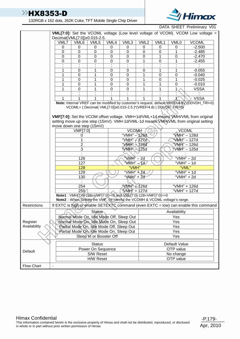
-P.179- Himax Confidential
Apr, 2010
This information contained herein is the exclusive property of Himax and shall not be distributed, reproduced, or disclosed in whole or in part without prior written permission of Himax.
HX8353-D 132RGB x 162 dots, 262K Color, TFT Mobile Single Chip Driver DATA SHEET Preliminary V01
VML[7:0]: Set the VCOML voltage (Low level voltage of VCOM). VCOM Low voltage = Decimal(VML[7:0])x0.015-2.5.
VML7 VML6 VML5 VML4 VML3 VML2 VML1 VML0 VCOML 0 0 0 0 0 0 0 0 -2.500 0 0 0 0 0 0 0 1 -2.485 0 0 0 0 0 0 1 0 -2.470 0 0 0 0 0 1 0 1 -2.455 : : : : : : : : : 1 0 1 0 0 0 1 1 -0.055 1 0 1 0 0 1 0 0 -0.040 1 0 1 0 0 1 0 1 -0.025 1 0 1 0 0 1 1 0 -0.010 1 0 1 0 0 1 1 1 VSSA : : : : : : : : 1 1 1 1 1 1 1 1 VSSA
Note: Internal VREF can be modified by customer’s request. default VREF=4.8V (DDVDH_TRI=0) VCOML= Decimal( VML[7:0])x0.015-2.5 *(VREF/4.8) ( DDVDH_TRI=0)
VMF[7:0]: Set the VCOM offset voltage. VMH+1d/VML+1d means VMH/VML from original setting move up one step (15mV). VMH-1d/VML-1d means VMH/VML from original setting move down one step (15mV)
VMF[7:0] VCOMH VCOML 0 “VMH” – 128d “VMH” – 128d 1 “VMH” – 127d “VMH” – 127d 2 “VMH” – 126d “VMH” – 126d 3 “VMH” – 125d “VMH” – 125d : : :
126 “VMH” – 2d “VMH” – 2d 127 “VMH” – 1d “VMH” – 1d 128 “VMH” “VML” 129 “VMH” + 1d “VMH” + 1d 130 “VMH” + 2d “VMH” + 2d
: : : 254 “VMH” + 126d “VMH” + 126d 255 “VMH” + 127d “VMH” + 127d
Note1 : VMH[7:0]-128+VMF[7:0]>=0 and VML[7:0]-128+VMF[7:0]>=0 Note2:When Setting the VMF, be careful the VCOMH & VCOML voltage’s range.
Restrictions If EXTC is high or enable SETEXTC command (even EXTC = low) can enable this command
Register Availability
Status Availability Normal Mode On, Idle Mode Off, Sleep Out Yes Normal Mode On, Idle Mode On, Sleep Out Yes Partial Mode On, Idle Mode Off, Sleep Out Yes Partial Mode On, Idle Mode On, Sleep Out Yes
Sleep In or Booster Off Yes
Default
Status Default Value Power On Sequence OTP value
S/W Reset No change H/W Reset OTP value
Flow Chart -

-P.180- Himax Confidential
Apr, 2010
This information contained herein is the exclusive property of Himax and shall not be distributed, reproduced, or disclosed in whole or in part without prior written permission of Himax.
HX8353-D 132RGB x 162 dots, 262K Color, TFT Mobile Single Chip Driver DATA SHEET Preliminary V01
8.2.43 SETEXTC: enable extension command (B9h)
B9 H SETEXTC ( Set Extended Command Set) DNC NWR NRD D17-8 D7 D6 D5 D4 D3 D2 D1 D0 HEX Command 0 ↑ 1 - 1 0 1 1 1 0 0 1 B9
1st parameter 1 ↑ 1 - EXTC1[7:0] 00 2nd parameter 1 ↑ 1 - EXTC2[7:0] 00 3rd parameter 1 ↑ 1 - EXTC3[7:0] 00
Description
This command is used to set extended command set access enable.
Extend cmd Command description
Enable After command (B9h), must write 3 parameters (FFh,83h,53h) by order
Disable(default) After command(B9h), write 3 parameters (xxh,xxh,xxh) any value is all right, but can not be (FFh,83h,53h)
Restrictions -
Register Availability
Status Availability Normal Mode On, Idle Mode Off, Sleep Out Yes Normal Mode On, Idle Mode On, Sleep Out Yes Partial Mode On, Idle Mode Off, Sleep Out Yes Partial Mode On, Idle Mode On, Sleep Out Yes
Sleep In or Booster Off Yes
Default
Status Default Value Power On Sequence EXTC1[7:0]=8’h00, EXTC2[7:0]=8’h00, EXTC3[7:0]=8’h00
S/W Reset No change H/W Reset EXTC1[7:0]=8’h00, EXTC2[7:0]=8’h00, EXTC3[7:0]=8’h00
Flow Chart -

-P.181- Himax Confidential
Apr, 2010
This information contained herein is the exclusive property of Himax and shall not be distributed, reproduced, or disclosed in whole or in part without prior written permission of Himax.
HX8353-D 132RGB x 162 dots, 262K Color, TFT Mobile Single Chip Driver DATA SHEET Preliminary V01
8.2.44 SETOTP: set OTP setting (BBh)
BB H SETOTP ( Set OTP related setting) DNC NWR NRD D17-8 D7 D6 D5 D4 D3 D2 D1 D0 HEX Command 0 ↑ 1 - 1 0 1 1 1 0 1 1 BB 1st parameter 1 ↑ 1 - OTP_MASK[7:0] 00 2nd parameter 1 ↑ 1 - OTP_INDEX[7:0] 00
3rd parameter 1 ↑ 1 -
OTP_LOAD_DISABL
E
DCCLK_DISABL
E
OTP_POR
OTP_PWE
OTP_EN
OTPTEST_EN
VPP_SEL
OTP_PRO
G 00
4th parameter 1 ↑ 1 - - - - - OTP_PTM[
1:0] OTP_VRAD
J[1:0] 00
5th parameter 1 1 ↑ - OTP_DATA[7:0] 00
Description
This command is used to set the OTP related setting. OTP_MASK7~OTP_MASK0: Bit programming mask, if 1, means don’t programming this bit OTP_INDEX7~OTP_INDEX0: Set location of OTP to be programmed OTP_EN: When written to 1, internal register begin written to OTP VPP_SEL: When written to 1, PVSS voltage is fed to OTP OTP_LOAD_DISABLE : When written to 1, auto load from OTP to internal register when SLPOUT command received is disabled, this is used when OTP is not yet programmed DCCLK_DISABLE: Disable Pumping Clock OTPTEST_EN:
0 : normal mode, automatic OTP programming mode (by internal state machine) 1 : manual mode 0 is the default value OTP_POR: for OTP read/write timing control OTP_PPROG : 1’b1 to turn on OTP write mode. OTP_PWE : 1’b1 to write OTP. OTP_PTM[1:0] : OTP Test mode register, In-house use. OTP_VRADJ[1:0] : OTP VPP2 adjusts register, In-house use. OTP_DATA[7:0] : OTP read data.
Restrictions If EXTC is high or enable SETEXTC command (even EXTC = low) can enable this command
Register Availability
Status Availability Normal Mode On, Idle Mode Off, Sleep Out Yes Normal Mode On, Idle Mode On, Sleep Out Yes Partial Mode On, Idle Mode Off, Sleep Out Yes Partial Mode On, Idle Mode On, Sleep Out Yes
Sleep In or Booster Off Yes
Default
Status Default Value
Power On Sequence
OTP_MASK[7:0]=8’h00, OTP_INDEX[7:0]=8’h00, OTP_LOAD_DISABLE=0, DCCLK_DISABLE=0, OTP_POR=0, OTP_PWE=0, OTP_EN=0, OTPTEST_EN=0, VPP_SEL=0, OTP_PROG=0, OTP_PTM[1:0]=2’b00, OTP_VRADJ[1:0]=2’b00
S/W Reset
OTP_MASK[7:0]=8’h00, OTP_INDEX[7:0]=8’h00, OTP_LOAD_DISABLE=0, DCCLK_DISABLE=0, OTP_POR=0, OTP_PWE=0, OTP_EN=0, OTPTEST_EN=0, VPP_SEL=0, OTP_PROG=0, OTP_PTM[1:0]=2’b00, OTP_VRADJ[1:0]=2’b00
H/W Reset
OTP_MASK[7:0]=8’h00, OTP_INDEX[7:0]=8’h00, OTP_LOAD_DISABLE=0, DCCLK_DISABLE=0, OTP_POR=0, OTP_PWE=0, OTP_EN=0, OTPTEST_EN=0, VPP_SEL=0, OTP_PROG=0, OTP_PTM[1:0]=2’b00, OTP_VRADJ[1:0]=2’b00
Flow Chart -

-P.182- Himax Confidential
Apr, 2010
This information contained herein is the exclusive property of Himax and shall not be distributed, reproduced, or disclosed in whole or in part without prior written permission of Himax.
HX8353-D 132RGB x 162 dots, 262K Color, TFT Mobile Single Chip Driver DATA SHEET Preliminary V01
8.2.45 SETVDC: set internal digital and GRAM voltag e (BCh)
BC H SETVDC (set internal digital and GRAM voltage) DNC NWR NRD D17-8 D7 D6 D5 D4 D3 D2 D1 D0 HEX Command 0 ↑ 1 - 1 0 1 1 1 1 0 0 BC
1st parameter 1 ↑ 1 - VDC_SEL[2:0] (100) 08
Description
This command is used to set internal digital and GRAM voltage. The VDC_SEL setting table:
Set VREF @ VDC_SEL[2:0] VDDD 0 0 0 1.28 0 0 1 1.34 0 1 0 1.38 0 1 1 1.44 1 0 0 1.5 1 0 1 1.6 1 1 0 1.7
1.8 V
1 1 1 1.8 Restrictions If EXTC is high or enable SETEXTC command (even EXTC = low) can enable this command
Register Availability
Status Availability Normal Mode On, Idle Mode Off, Sleep Out Yes Normal Mode On, Idle Mode On, Sleep Out Yes Partial Mode On, Idle Mode Off, Sleep Out Yes Partial Mode On, Idle Mode On, Sleep Out Yes
Sleep In or Booster Off Yes
Default
Status Default Value Power On Sequence VDC_SEL[2:0]=100
S/W Reset No change H/W Reset VDC_SEL[2:0]=100
Flow Chart -

-P.183- Himax Confidential
Apr, 2010
This information contained herein is the exclusive property of Himax and shall not be distributed, reproduced, or disclosed in whole or in part without prior written permission of Himax.
HX8353-D 132RGB x 162 dots, 262K Color, TFT Mobile Single Chip Driver DATA SHEET Preliminary V01
8.2.46 SETSTBA: set source option (C0h)
C0 H SETSTBA ( Set Source Option) DNC NWR NRD D17-8 D7 D6 D5 D4 D3 D2 D1 D0 HEX Command 0 ↑ 1 - 1 1 0 0 0 0 0 0 C0
1st parameter 1 ↑ 1 - N_OPON[7:0] 18 2nd parameter 1 ↑ 1 - I_OPON[7:0] 08 3rd parameter 1 ↑ 1 - STBA[15:8] 0C 4th parameter 1 ↑ 1 - STBA[7:0] C4 5th parameter 1 ↑ 1 - GENON[7:0] 10 6th parameter 1 ↑ 1 - - - - - - - - OTP_S1B 00
Description This command is used to set source option setting. Internal used, not open.
Restrictions If EXTC is high or enable SETEXTC command (even EXTC = low) can enable this command
Register Availability
Status Availability Normal Mode On, Idle Mode Off, Sleep Out Yes Normal Mode On, Idle Mode On, Sleep Out Yes Partial Mode On, Idle Mode Off, Sleep Out Yes Partial Mode On, Idle Mode On, Sleep Out Yes
Sleep In or Booster Off Yes
Default
Status Default Value
Power On Sequence N_OPON[7:0]=8’h20, I_OPON[7:0]=8’h10, STBA[15:0]=16’h0000, GENON[7:0]=8’h16, OTP_S1B=0
S/W Reset No change
H/W Reset N_OPON[7:0]=8’h20, I_OPON[7:0]=8’h10, STBA[15:0]=16’h0000, GENON[7:0]=8’h16, OTP_S1B=0
Flow Chart -

-P.184- Himax Confidential
Apr, 2010
This information contained herein is the exclusive property of Himax and shall not be distributed, reproduced, or disclosed in whole or in part without prior written permission of Himax.
HX8353-D 132RGB x 162 dots, 262K Color, TFT Mobile Single Chip Driver DATA SHEET Preliminary V01
8.2.47 SETTID: set ID (C3h)
C3 H SETID ( Set ID) DNC NWR NRD D17-8 D7 D6 D5 D4 D3 D2 D1 D0 HEX Command 0 ↑ 1 - 1 1 0 0 0 0 1 1 C3
1st parameter 1 ↑ 1 - ID1[7:0] 00 2nd parameter 1 ↑ 1 - ID2[7:0] 80 3rd parameter 1 ↑ 1 - ID3[7:0] 00 Description This command is used to set ID. Restrictions If EXTC is high or enable SETEXTC command (even EXTC = low) can enable this command
Register Availability
Status Availability Normal Mode On, Idle Mode Off, Sleep Out Yes Normal Mode On, Idle Mode On, Sleep Out Yes Partial Mode On, Idle Mode Off, Sleep Out Yes Partial Mode On, Idle Mode On, Sleep Out Yes
Sleep In or Booster Off Yes
Default
Status Default Value Power On Sequence OTP value
S/W Reset No Change H/W Reset OTP value
Flow Chart -

-P.185- Himax Confidential
Apr, 2010
This information contained herein is the exclusive property of Himax and shall not be distributed, reproduced, or disclosed in whole or in part without prior written permission of Himax.
HX8353-D 132RGB x 162 dots, 262K Color, TFT Mobile Single Chip Driver DATA SHEET Preliminary V01
8.2.48 SETUADJ: (C6h)
C6 H SETUADJ DNC NWR NRD D17-8 D7 D6 D5 D4 D3 D2 D1 D0 HEX Command 0 ↑ 1 - 1 1 0 0 0 1 1 0 C6
1st parameter 1 ↑ 1 - - I_UADJ[2:0] - N_UADJ[2:0] 33 Description This command is used to set UADJ. Restrictions If EXTC is high or enable SETEXTC command (even EXTC = low) can enable this command
Register Availability
Status Availability Normal Mode On, Idle Mode Off, Sleep Out Yes Normal Mode On, Idle Mode On, Sleep Out Yes Partial Mode On, Idle Mode Off, Sleep Out Yes Partial Mode On, Idle Mode On, Sleep Out Yes
Sleep In or Booster Off Yes
Default
Status Default Value Power On Sequence I_UADJ[2:0]=03 ; N_UADJ[2:0]=03
S/W Reset No Change H/W Reset I_UADJ[2:0]=03 ; N_UADJ[2:0]=03
Flow Chart -
UADJUADJUADJUADJ Trimming FreqTrimming FreqTrimming FreqTrimming Freq
0 0 0 228.6%
0 0 1 123.9%
0 1 0 112.0%
0 1 1 100.0%
1 0 0 87.9%
1 0 1 75.8%
1 1 0 63.6%
1 1 1 51.3%

-P.186- Himax Confidential
Apr, 2010
This information contained herein is the exclusive property of Himax and shall not be distributed, reproduced, or disclosed in whole or in part without prior written permission of Himax.
HX8353-D 132RGB x 162 dots, 262K Color, TFT Mobile Single Chip Driver DATA SHEET Preliminary V01
8.2.49 SETCLOCK: (CBh)
CB H SETECO DNC NWR NRD D17-8 D7 D6 D5 D4 D3 D2 D1 D0 HEX Command 0 ↑ 1 - 1 1 0 0 1 0 1 1 CB
1st parameter 1 ↑ 1 - CADJ[3:0] - - - - 20
2nd parameter 1 ↑ 1 - - - - - - - - DCCLK_SYNC 01
Description This command is used to set CLOCK. Restrictions If EXTC is high or enable SETEXTC command (even EXTC = low) can enable this command
Register Availability
Status Availability Normal Mode On, Idle Mode Off, Sleep Out Yes Normal Mode On, Idle Mode On, Sleep Out Yes Partial Mode On, Idle Mode Off, Sleep Out Yes Partial Mode On, Idle Mode On, Sleep Out Yes
Sleep In or Booster Off Yes
Default
Status Default Value Power On Sequence CADJ[3:0] (1000) ; DCCLK_SYNC(1)
S/W Reset No Change H/W Reset CADJ[3:0] (1000) ; DCCLK_SYNC(1)
Flow Chart -
CADJ[3:0] Trimming Freq
0000 111.9% 0001 110.3% 0010 108.7% 0011 107.1% 0100 105.7% 0101 104.1% 0110 102.7% 0111 101.3% 1000 100.0% 1001 98.6% 1010 97.4% 1011 96.2% 1100 94.9% 1101 93.7% 1110 92.6% 1111 91.5%

-P.187- Himax Confidential
Apr, 2010
This information contained herein is the exclusive property of Himax and shall not be distributed, reproduced, or disclosed in whole or in part without prior written permission of Himax.
HX8353-D 132RGB x 162 dots, 262K Color, TFT Mobile Single Chip Driver DATA SHEET Preliminary V01
8.2.50 SETPANEL: set panel characteristic (CCh)
CCH SETPANEL( Set Panel Characteristic Register) DNC NWR NRD D17-8 D7 D6 D5 D4 D3 D2 D1 D0 HEX Command 0 ↑ 1 - 1 1 0 0 1 1 0 0 CC
1st parameter 1 ↑ 1 - - - - - SS_PANEL
GS_PANEL
REV_PANE
L
BGR_PANEL
00
Description
This command is used to set Panel characteristic related register REV_PANEL: The source output data polarity selected. When REV_PANEL=0, normally white panel is selected. When REV_PANEL = 1, normally black panel is selected. BGR_PANEL: The color filter order direction selected. When BGR_PANEL=0, don’t reverse the SRGB setting. When BGR_PANEL = 1, the color filter order will be reversed. GS_PANEL: The gate driver output shift direction selected. When GS_PANEL=0, the shift direction don’t reverse. When GS_PANEL = 1, the shift direction will be reversed. SS_PANEL: The source driver output shift direction selected. When SS_PANEL=0, the shift direction don’t reverse. When SS_PANEL = 1, the shift direction will be reversed.
Restrictions If EXTC is high or enable SETEXTC command (even EXTC = low) can enable this command
Register Availability
Status Availability Normal Mode On, Idle Mode Off, Sleep Out Yes Normal Mode On, Idle Mode On, Sleep Out Yes Partial Mode On, Idle Mode Off, Sleep Out Yes Partial Mode On, Idle Mode On, Sleep Out Yes
Sleep In or Booster Off Yes
Default
Status Default Value
Power On Sequence SS_PANEL=0, GS_PANEL=0, REV_PANEL=0, BGR_PANEL=0
S/W Reset No change
H/W Reset SS_PANEL=0, GS_PANEL=0, REV_PANEL=0, BGR_PANEL=0
Flow Chart -

-P.188- Himax Confidential
Apr, 2010
This information contained herein is the exclusive property of Himax and shall not be distributed, reproduced, or disclosed in whole or in part without prior written permission of Himax.
HX8353-D 132RGB x 162 dots, 262K Color, TFT Mobile Single Chip Driver DATA SHEET Preliminary V01
8.2.51 GETHID: Read Product ID (D0h)
D0H GETHID (Read Product ID) DNC NWR NRD D17-8 D7 D6 D5 D4 D3 D2 D1 D0 HEX Command 0 ↑ 1 - 1 1 0 1 0 0 0 0 D0
1st parameter 1 ↑ 1 - Dummy Read xx 2st parameter 1 ↑ 1 - Product ID [7:0] (0110_0100) 64 Description This command is used to Read Product ID Restrictions If EXTC is high or enable SETEXTC command (even EXTC = low) can enable this command
Register Availability
Status Availability Normal Mode On, Idle Mode Off, Sleep Out Yes Normal Mode On, Idle Mode On, Sleep Out Yes Partial Mode On, Idle Mode Off, Sleep Out Yes Partial Mode On, Idle Mode On, Sleep Out Yes
Sleep In or Booster Off Yes
Default
Status Default Value Power On Sequence Product ID [7:0]=64H
S/W Reset No change H/W Reset Product ID [7:0]=64H
Flow Chart -
-P.189- Himax Confidential
Apr, 2010
This information contained herein is the exclusive property of Himax and shall not be distributed, reproduced, or disclosed in whole or in part without prior written permission of Himax.
HX8353-D 132RGB x 162 dots, 262K Color, TFT Mobile Single Chip Driver DATA SHEET Preliminary V01
8.2.52 SETGAMMA: set gamma curve (E0h) E0H SETGAMMA ( Set Gamma Curve Related Setting) DNC NWR NRD D17-8 D7 D6 D5 D4 D3 D2 D1 D0 HEX Command 0 ↑ 1 - 1 1 1 0 0 0 0 0 E0
1st parameter 1 ↑ 1 - - MP1[2:0] - MP0[2:0] 77 2nd parameter 1 ↑ 1 - - MP3[2:0] - MP2[2:0] 73 3rd parameter 1 ↑ 1 - - MP5[2:0] - MP4[2:0] 00 4th parameter 1 ↑ 1 - - - - - CP0[3:0] 0D 5th parameter 1 ↑ 1 - CP2[3:0] CP1[3:0] 4F 6th parameter 1 ↑ 1 - - - - - CP3[3:0] 08 7th parameter 1 ↑ 1 - - - - - CP4[3:0] 09 8th parameter 1 ↑ 1 - - - - - OP0[3:0] 00 9th parameter 1 ↑ 1 - - - - OP1[4:0] 0F 10th parameter 1 ↑ 1 - - - - - CGM1[1:0] CGM0[1:0] 0A 11st parameter 1 ↑ 1 - - MN1[2:0] - MN0[2:0] 77 12nd parameter 1 ↑ 1 - - MN3[2:0] - MN2[2:0] 40 13rd parameter 1 ↑ 1 - - MN5[2:0] - MN4[2:0] 00 14th parameter 1 ↑ 1 - - - - - CN0[3:0] 09 15th parameter 1 ↑ 1 - CN2[3:0] CN1[3:0] 48 16th parameter 1 ↑ 1 - - - - - CN3[3:0] 0F 17th parameter 1 ↑ 1 - - - - - CN4[3:0] 0D 18th parameter 1 ↑ 1 - - - - - ON0[3:0] 0F 19th parameter 1 ↑ 1 - - - - ON1[4:0] 00
Description This command is used for Gamma Curve related Setting. For details, please refer to Section 7.2.
Restrictions If EXTC is high or enable SETEXTC command (even EXTC = low) can enable this command
Register Availability
Status Availability Normal Mode On, Idle Mode Off, Sleep Out Yes Normal Mode On, Idle Mode On, Sleep Out Yes Partial Mode On, Idle Mode Off, Sleep Out Yes Partial Mode On, Idle Mode On, Sleep Out Yes
Sleep In or Booster Off Yes
Default
Status Default Value Power On Sequence GC0 value
S/W Reset No change H/W Reset GC0 value
Flow Chart -
-P.190- Himax Confidential
Apr, 2010
This information contained herein is the exclusive property of Himax and shall not be distributed, reproduced, or disclosed in whole or in part without prior written permission of Himax.
HX8353-D 132RGB x 162 dots, 262K Color, TFT Mobile Single Chip Driver DATA SHEET Preliminary V01
8.2.53 SETEQ: set EQ (E3h)
E3H SETEQ( Set EQ) DNC NWR NRD D17-8 D7 D6 D5 D4 D3 D2 D1 D0 HEX
Command 0 ↑ 1 - 1 1 1 0 0 0 1 1 E3 1st parameter 1 ↑ 1 - EQVCI_M1[7:0] 18 2nd parameter 1 ↑ 1 - EQGND_M1[7:0] 08 3rd parameter 1 ↑ 1 - EQVCI_M0[7:0] 00 4th parameter 1 ↑ 1 - EQGND_M0[7:0] 08 5th parameter 1 ↑ 1 - PREOE_M0[7:0] 00 6th parameter 1 ↑ 1 - PREOE_M1[7:0] 00 Description Internal used, not open. Restrictions If EXTC is high or enable SETEXTC command (even EXTC = low) can enable this command
Register Availability
Status Availability Normal Mode On, Idle Mode Off, Sleep Out Yes Normal Mode On, Idle Mode On, Sleep Out Yes Partial Mode On, Idle Mode Off, Sleep Out Yes Partial Mode On, Idle Mode On, Sleep Out Yes
Sleep In or Booster Off Yes
Default
Status Default Value
Power On Sequence EQVCI_M1[7:0]=8’h10, EQGND_M1[7:0]=8’h08, EQVCI_M0[7:0]=8’h08, EQGND_M0[7:0]=8’h10, PREOE_M0[7:0]=8’h00, PREOE_M1[7:0]=8’h00
S/W Reset No change
H/W Reset EQVCI_M1[7:0]=8’h10, EQGND_M1[7:0]=8’h08, EQVCI_M0[7:0]=8’h08, EQGND_M0[7:0]=8’h10, PREOE_M0[7:0]=8’h00, PREOE_M1[7:0]=8’h00
Flow Chart -
-P.191- Himax Confidential
Apr, 2010
This information contained herein is the exclusive property of Himax and shall not be distributed, reproduced, or disclosed in whole or in part without prior written permission of Himax.
HX8353-D 132RGB x 162 dots, 262K Color, TFT Mobile Single Chip Driver DATA SHEET Preliminary V01
9. Layout Recommendation
Display Panel
OSC
BS0
BS1
VSSD
P68
IOVCC
DUMMYVSSD
DUMMY
IOVCC
BGR_PANEL
VSSD
TEST1
VCI
VCI
VCI
VCI
VSSA
VSSD
STE_SCL
DB17
DB16
DB15
DB14
DB5
DB7
TE
NRESET
NCS
BS2
DB4
DB0_SDA
DB6
NWR_RNW
DUMMY
DUMMY
DUMMY
DUMMY
TS2
TS1
TS0
VSSD
VSSD
VSSD
VSSD
VSSD
VSSD
IOVCC
IOVCC
IOVCC
IOVCC
IOVCC
VDDD
IOVCC
VDDD
VDDD
DUMMY
DUMMY
VBGP
VBGP
VBGP
DUMMY
DDVDH
DDVDH
DDVDH
DDVDH
DDVDH
VREG1
VREG1
VREG1
DUMMYR1
C11A
C11A
C11A
C11A
DUMMYR2
C11B
C11B
C11B
DUMMY
DUMMY
DUMMY
DUMMY
DUMMY
DUMMY
VSSA
VSSA
VSSA
VCL
VCL
VCL
VGL
VGL
VGL
VGH
VCOMH
VGH
VCOMH
VCOMH
VGH
VCOML
VCOML
VCOM
VCOML
VCOM
VCOM
DUMMY
IOVCC
C11B
DUMMY
DUMMY
DUMMY
DUMMY
DUMMY No. 759
Face Up(Bump view)
HX8353-DPin Assignment
No.1 TS7
IOVCC
EXTC
VSSD
G162
G160
X
Y(0,0)
TEST2
10 ohm
SS_PANEL
GS_PANEL
REV_PANEL
SS_PANEL
IOVCC
GS_PANEL
VSSDDUMMY
IOVCCREV_PANEL
VSSD
DUMMY
IOVCC
DUMMY
VSSD
DUMMYIOVCC
LC_SEL0VSSD
LC_SEL1
IOVCCRSO2
VSSD
RSO1
IOVCC
RSO0
VSSD
DUMMY
GC_SEL
SPI_SEL
IOVCC
TS6
TS5
TS4
TS3
OSC
VCIVCI
VSSA
VSSA
VSSA
VSSA
VSSA
NRD_E
DNC_SCL
DB13
DB12
DB11
DB10
DB9
DB8
DB1
DB3
DB2
G158
G156
G154
G152
G150
G148
G8
G6
G4
G2
DUMMY
DUMMY
DUMMY
DUMMY
S396
S395
S394
G161
G159
G157
G155
G153
G151
G149
G147
G7
G5
G3
G1
DUMMY
DUMMY
DUMMY
DUMMY
S1
S2
S3
S4
S393
Alignmentmark(4841,-220)
100 ohm
100 ohm
100 ohm
100 ohm
100 ohm
100 ohm
10 ohm
10 ohm
10 ohm
50 ohm
10 ohm
EXTC
BS0
P68
BGR_PANEL
BS1
TEST1
VCI
TE
DUMMY No. 186
Alignmentmark(-4841,-220)
No. 185
10 ohm
100 ohm
100 ohm
100 ohm
100 ohm
S202
S201
S200
S199
DUMMY
DUMMY
DUMMY
DUMMY
S198
S197
S196
S195
10 ohm
10 ohm
10 ohm
10 ohm
10 ohm
10 ohm
10 ohm
10 ohm
10 ohm
10 ohm
10 ohm
10 ohm
10 ohm
LC_SEL0 100 ohm
100 ohmLC_SEL1
10 ohm
10 ohm
RSO2 100 ohm
100 ohmRSO1
10 ohm
10 ohm
RSO0 100 ohm
100 ohmGC_SEL
10 ohm
10 ohm
100 ohmSPI_SEL
10 ohm
100 ohmNRD_E
100 ohmDNC_SEL
100 ohmSTE_SEL
10 ohm
100 ohmDB17
100 ohmDB16
100 ohmDB15
100 ohmDB14
100 ohmDB13
100 ohmDB12
100 ohmDB11
100 ohmDB10
100 ohmDB9
100 ohmDB8
100 ohmDB1
100 ohmDB3
100 ohmDB5
100 ohmDB7
100 ohm
100 ohmNRESET
100 ohmNCS
100 ohmDB6
100 ohmDB4
100 ohmDB2
100 ohmBS2
100 ohmDB0_SDA
100 ohmNWR_NWR
10 ohm
10 ohmIOVCC
100 ohm
100 ohmTEST2
100 ohm
100 ohm
10 ohm
10 ohm
10 ohm
10 ohm
10 ohm
10 ohm
10 ohm
10 ohm
10 ohm
VTESTOUT 100 ohm VTESTOUT
10 ohm
10 ohm
100 ohm
100 ohm
VDDD
VBGP
VREG1
VGL
VGH
VCOMH
VCOML
DUMMY
DUMMY
Figure 9.1 Layout recommendation of HX8353-D

-P.192- Himax Confidential
Apr, 2010
This information contained herein is the exclusive property of Himax and shall not be distributed, reproduced, or disclosed in whole or in part without prior written permission of Himax.
HX8353-D 132RGB x 162 dots, 262K Color, TFT Mobile Single Chip Driver DATA SHEET Preliminary V01
Maximum layout resistance
Name Type Maximum Series Resistance Unit
VCI Power supply 10 Ω IOVCC Power supply 10 Ω VSSA Power supply 10 Ω VSSD Power supply 10 Ω OSC Input 100 Ω EXTC Input 100 Ω
P68, BS2, BS1, BS0 Input 100 Ω STE_SEL, GC_SEL, SPI_SEL Input 100 Ω
RSO0, RSO1, RSO2 Input 100 Ω LC_SEL0, LC_SEL1 Input 100 Ω
NRESET, NCS, DNC_SCL Input 100 Ω NWR_RNW, NRD_E Input 100 Ω
TEST2, TEST1 Input 100 Ω SS_PANEL, GS_PANEL, REV_PANEL,
BGR_PANEL Input 100 Ω
DUMMYR1,DUMMYR2, Input 100 Ω DB0_SDA, DB17 ~ DB1 Input / Output 100 Ω
VGH Output 10 Ω VGL Output 10 Ω
C11A, C11B Output 10 Ω C12A, C12B Output 10 Ω C22A, C22B Output 10 Ω C21A, C21B Output 10 Ω
VDDD Output 10 Ω DDVDH Output 10 Ω
VCL Output 10 Ω TE Output 100 Ω
VCOMH, VCOML Output 100 Ω VREG1 Output 100 Ω VBGP Output 100 Ω
VTESTOUT Output 100 Ω Table 9.1 Maximum layout resistance

-P.193- Himax Confidential
Apr, 2010
This information contained herein is the exclusive property of Himax and shall not be distributed, reproduced, or disclosed in whole or in part without prior written permission of Himax.
HX8353-D 132RGB x 162 dots, 262K Color, TFT Mobile Single Chip Driver DATA SHEET Preliminary V01
10. OTP Programming
OTP_INDEX D7 D6 D5 D4 D3 D2 D1 D0 Non-Program 00h ID17 ID16 ID15 ID14 ID13 ID12 ID11 ID10 00h 01h ID27 ID26 ID25 ID24 ID23 ID22 ID21 ID20 00h 02h ID37 ID36 ID35 ID34 ID33 ID32 ID31 ID30 00h 03h VMF17 VMF16 VMF15 VMF14 VMF13 VMF12 VMF11 VMF10 00h 04h VMF27 VMF26 VMF25 VMF24 VMF23 VMF22 VMF21 VMF20 00h 05h VMF37 VMF36 VMF35 VMF34 VMF33 VMF32 VMF31 VMF30 00h
06h - - - - - Valid_VM
F3 Valid_VM
F2 Valid_VM
F1 00h
07h Valid_ID - - - - - - - 00h
Table 10.1 OTP address mapping Note: (1) The default value of OTP memory bits are all “0”.
(2) “Valid_ID” bit decide the OTP reload Enable/Disable, the default value is “0”. If the OTP index of Valid bit had been programmed, the Valid bit will be changed to “1” automatically and execute the OTP reload.
(3) Please set the 00h(ID1) & 01h(ID2) & 02h(ID3) at the same time. (4) VMF can be programmed three times. When programming index 03h first time, VMF1 and
Valid_VMF1 will be programmed automatically. If programming index 03h second time, VMF2 and Valid_VMF2 will be programmed automatically. If programming index 03h third time, VMF3 and Valid_VMF3 will be programmed automatically.
(5) The OTP programming (External 6.5V to VGH) current limit must ≧20mA. For example: Condition 1: Programmed all index of 0X00h, 0X01h and 0X02h

-P.194- Himax Confidential
Apr, 2010
This information contained herein is the exclusive property of Himax and shall not be distributed, reproduced, or disclosed in whole or in part without prior written permission of Himax.
HX8353-D 132RGB x 162 dots, 262K Color, TFT Mobile Single Chip Driver DATA SHEET Preliminary V01
Condition 2: Do not program all index of 0X00h, 0X01h and 0X02h
(4) There are some conditions that HX8353-D can reload OTP. 1.Hardware reset 2.Software reset 3.SLPOUT command.
(5) User can use GETOTP command to read back the OTP values. Similarly, the user also can use GETOTP to read the index 0x06h that is defined the VALID bit for VMF1, VMF2 and VMF3 (Valid_VMF1, Valid_VMF2 and Valid_VMF3) to know how many times of VMF had programmed on OTP.
Valid_VMF3 Valid_VMF2 Valid_VMF1
Programmed 0 time 0 0 0
Programmed 1 time 0 0 1
Programmed 2 times 0 1 1
Programmed 3 times 1 1 1

-P.195- Himax Confidential
Apr, 2010
This information contained herein is the exclusive property of Himax and shall not be distributed, reproduced, or disclosed in whole or in part without prior written permission of Himax.
HX8353-D 132RGB x 162 dots, 262K Color, TFT Mobile Single Chip Driver DATA SHEET Preliminary V01
10.1 Programming flow

-P.196- Himax Confidential
Apr, 2010
This information contained herein is the exclusive property of Himax and shall not be distributed, reproduced, or disclosed in whole or in part without prior written permission of Himax.
HX8353-D 132RGB x 162 dots, 262K Color, TFT Mobile Single Chip Driver DATA SHEET Preliminary V01
10.2 OTP Programming example for VMF1
SLPOUT (R11H)
Set DCCLK_Disable = 1
(RBBH = 0x00H、0x00H、0x40H、0x00H、0x00H)
Connect external power 6.5V to VGH
Set OTP_EN = 1
(RBBH = 0x00H、0x03H、0x48H)
Delay 1mS for OTP program
H/W Reset
VMF1 Program Flow
Yes
No
END
Wait 120mS
Power On
Program another VMF value
Remove external power 6.5V to VGH
Reset IC to reload OTP data
Wait 5mS
SETEXTC
(RB9H = 0xFFH、0x83H、0x53H)
SET VMF
(RB6H = 0x??H、VMH、VML)
Set OTP_EN = 0
(RBBH = 0x00H、0x03H、0x40H)

-P.197- Himax Confidential
Apr, 2010
This information contained herein is the exclusive property of Himax and shall not be distributed, reproduced, or disclosed in whole or in part without prior written permission of Himax.
HX8353-D 132RGB x 162 dots, 262K Color, TFT Mobile Single Chip Driver DATA SHEET Preliminary V01
10.3 Programming sequence
Step Operation 1 Power on and reset the module 2 Set OTP_LOAD_DISABLE=1, disable the auto-loading function. 3 SLPOUT command (11h) 4 Wait 120ms 5 Write optimized value to related register. 6 Set OSC_EN=0, disable internal pumping clock. 7 Connect external power 6.5V to VGH pin 8 Wait 100ms for external power 6.5V to stabilize. 9 Specify OTP_index. Reference OTP address mapping table 10 Set OTP_Mask=0x00h, programming the entire bit of one parameter. 11 Set OTP_EN=1, Internal register begin write to OTP according to OTP_index. 12 Wait 1 ms
13 Complete programming one parameter to OTP. If continue to programming other parameter, return to step (9). Otherwise, power off the module and remove the external power on VGH pin.
10.4 OTP Read flow and example
Display On (R29H)
SLPOUT (R11H)
H/W Reset
Wait 120mS
Power On
Wait 5mS
Read VMF OTP value
(RB6H = VMF、VMH、VML)
VMF
Programmed
VMF not
Programmed
0x??H0x9EH
or
Initial code setting
SETEXTC
(RB9H = 0xFFH、0x83H、0x53H)

-P.198- Himax Confidential
Apr, 2010
This information contained herein is the exclusive property of Himax and shall not be distributed, reproduced, or disclosed in whole or in part without prior written permission of Himax.
HX8353-D 132RGB x 162 dots, 262K Color, TFT Mobile Single Chip Driver DATA SHEET Preliminary V01
10.5 Programming circuitry

-P.199- Himax Confidential
Apr, 2010
This information contained herein is the exclusive property of Himax and shall not be distributed, reproduced, or disclosed in whole or in part without prior written permission of Himax.
HX8353-D 132RGB x 162 dots, 262K Color, TFT Mobile Single Chip Driver DATA SHEET Preliminary V01
11. Electrical Characteristic
11.1 Absolute maximum ratings
Item Symbol Unit Value Note Power Supply Voltage 1 IOVCC~VSSD V -0.3 to +4.6 Note(1),(2) Power Supply Voltage 2 VCI ~ VSSA V -0.3 to +4.6 Note(3) Power Supply Voltage 3 DDVDH ~ VSSA V -0.3 to +6.6 Note(4) Power Supply Voltage 4 VSSA ~ VCL V -0.3 to +4.6 Note(5) Power Supply Voltage 5 DDVDH ~ VCL V -0.3 to +9 Note(6) Power Supply Voltage 6 VGH ~ VSSA V -0.3 to +18.5 Note(7) Power Supply Voltage 7 VSSA ~ VGL V 0 to -16 Note(8) Logic Input Voltage VIN V -0.3 to IOVCC+0.5 - Logic Output Voltage Vo V -0.3 to IOVCC+0.5 - Operating Temperature Topr -30 to +80 Note(9),(10) Storage Temperature Tstg -55 to +110 Note(9),(10)
Note: (1) IOVCC, VSSD must be maintained. (2) To make sure IOVCC ≥ VSSD. (3) To make sure VCI ≥ VSSA. (4) To make sure DDVDH ≥ VSSA. (5) To make sure VSSA ≥ VCL. (6) To make sure DDVDH ≥ VCL. (7) To make sure VGH ≥ VSSA. (8) To make sure VSSA ≥ VGL
VGH +|VGL| < 32V (9) For die and wafer products, specified up to +80 .
Table 11.1 Absolute maximum ratings 11.2 ESD protection level
Mode Test Condition Protection Level Unit Human Body Model C=100pF, R=1.5kΩ ±2.0K V Machine Model C=200pF, R=0.0Ω ±200 V
Table 11.2 ESD protection level

-P.200- Himax Confidential
Apr, 2010
This information contained herein is the exclusive property of Himax and shall not be distributed, reproduced, or disclosed in whole or in part without prior written permission of Himax.
HX8353-D 132RGB x 162 dots, 262K Color, TFT Mobile Single Chip Driver DATA SHEET Preliminary V01
11.3 DC characteristics
Spec. Parameter Symbol Conditions
Min. Typ. Max. Unit
Power & Operating Voltages IO Operating voltage IOVCC I/O supply voltage 1.65 1.8 3.3 Driver Operating voltage VCI Operation voltage 2.5 2.8 3.3
Source Drive Voltage VREG1 Dual Pump 3.3 4.65 4.8
VCI=2.8 Dual Pump (Typ:BT=000) - - -
IVGH=30µA 9.5 10 10.5 IVGH=25µA 10.3 10.8 11.3 IVGH=20µA 11.25 11.5 11.75 IVGH=15µA 11.75 12 12.25 IVGH=10µA 12.25 12.5 12.75
Gate Drive High Voltage VGH
IVGH=5µA 13 13.25 13.5 VCI=2.8 Dual Pump
(Typ:BT=000) - - -
IVGL=30µA -8.05 -8.2 -8.35 IVGL=25µA -8.75 -8.9 -9.05 IVGL=20µA -9.25 -9.4 -9.55 IVGL=15µA -9.75 -9.9 -10.05 IVGL=10µA -10.35 -10.5 -10.65
Gate Drive Low Voltage VGL
IVGL=5µA -10.85 -11 -11.15 Drive Supply Voltage |VGH-VGL| - - - 30
V
Input / Output High level input voltage VIH - 0.7*IOVCC - IOVCC Low level input voltage VIL - VSSD - 0.3*IOVCC High level output voltage VOH IOH = -1.0mA 0.8*IOVCC - IOVCC
Low level output voltage VOL IOL = +1.0mA VSSD - 0.2*IOVCC
V
Input leakage current IIL - -1 - 1 µA
Oscillator frequency fOSC
Frame rate at 75hz,default Vs and
Hs setting TA=25
1.387 1.46 1.533 MHz
Booster (VCI=2.8V)
DDVDH boost voltage1 DDVDH Dual Pump
IDDVDH=300µA 4.8 5.0 5.2
VCL boost voltage VCL ICL=-100µA -2.5 -2.65 2.75 V
VCOM Generator (VCI=2.8V)
VCOM amplitude VCOM No load, Dual Pump 2.5 4.4 7.3 V
VCOM high level VCOMH No load, Dual Pump 2.5 3.205 4.8 V
VCOM low level VCOML No load -2.5 -1.195 VSSD V Source Driver (Typ:T A=25 VCI=2.8 V)
VSSD+1.0 ~ VREG1-1.0 - +/- 10 +/- 20 mV
Output voltage deviation (mean value)
DVOS VSSD+0.1V ~ VSSD+1.0
VREG1-1.0 ~ VREG1-0.1V
- +/- 30 +/- 50 mV
Output voltage range VOS - 0.1 - DDVDH-0.1 V Output offset voltage Voff - +/-30 +/-50 mV
Note: VREG1/VCOMH/VCOML conditions: When Internal Voltage VREF=4.8V for dual pump

-P.201- Himax Confidential
Apr, 2010
This information contained herein is the exclusive property of Himax and shall not be distributed, reproduced, or disclosed in whole or in part without prior written permission of Himax.
HX8353-D 132RGB x 162 dots, 262K Color, TFT Mobile Single Chip Driver DATA SHEET Preliminary V01
FPC
Measurement point
LCD Panel
Measurement point
Connector pin or flex side

-P.202- Himax Confidential
Apr, 2010
This information contained herein is the exclusive property of Himax and shall not be distributed, reproduced, or disclosed in whole or in part without prior written permission of Himax.
HX8353-D 132RGB x 162 dots, 262K Color, TFT Mobile Single Chip Driver DATA SHEET Preliminary V01
11.3.1 Current consumption
Current consumption Typical Worst case Host
I/F Mode of
operation Frame
Frequency Inversion
Mode Image
Memory Data
Access Control
(MY:MX:MV)
VCI (mA)
IOVCC (uA)
VCI (mA)
IOVCC(uA)
1-line Black X;X;X 1.2 2.5 1.48 3
1-line 1x1 checker board X;X;X 1.17 2.5 1.45 3
1-line 4x4 checker board X;X;X 1.25 2.5 1.46 3
1-line Grayscale
Top to Bottom
X;X;X 1.18 2.5 1.4 3
- Normal Mode On - Partial Mode Off - Idle Mode Off - Sleep Out Mode
60Hz
1-line 20B80W X;X;X 1.14 2.5 1.3 3 - Normal Mode On - Partial Mode Off - Idle Mode On - Sleep Out Mode
60Hz 1-line 20B80W X;X;X 0.67 2.5 0.77 3
- Normal Mode Off - Partial Mode On (32 lines) - Idle Mode Off - Sleep Out Mode
60Hz 1-line Grey Levels X;X;X 0.72 2.5 0.82 3
1-line 8x8 checker board X;X;X 0.52 2.5 0.58 3
- Normal Mode Off - Partial Mode On (32 lines) - Idle Mode On - Sleep Out Mode
60Hz 1-line Worst
pattern X;X;X 0.55 2.5 0.62 3
- Sleep In Mode N/A N/A N/A X;X;X 2µA 2.5 80µA 10
Hos
t int
erfa
ce N
OT
act
ive
- Deep Sleep In Mode
N/A N/A N/A X;X;X 0.1µA 0.1 1µA 1
0;0;0 1.28 3 1.5 7 0;0;1 1.28 3 1.5 7 0;1;0 1.28 3 1.5 7 0;1;1 1.28 3 1.5 7 1;0;0 1.28 3 1.5 7 1;0;1 1.28 3 1.5 7 1;1;0 1.28 3 1.5 7
262k Colors Worst pattern CPU
Access @ 15fps
1;1;1 1.28 3 1.5 7 0;0;0 1.3 3 1.55 12 0;0;1 1.3 3 1.55 12 0;1;0 1.3 3 1.55 12 0;1;1 1.3 3 1.55 12 1;0;0 1.3 3 1.55 12 1;0;1 1.3 3 1.55 12 1;1;0 1.3 3 1.55 12
Hos
t int
erfa
ce a
ctiv
e
- Normal Mode On - Partial Mode Off - Idle Mode Off - Sleep Out Mode
60Hz 1-line
262k Colors Worst pattern CPU
Access @ 25fps
1;1;1 1.3 3 1.55 12 Table 11.3 Current consumption
Typical Case: TA = 25°C IOVCC=1.8V VCI = 2.8V Worst Case: TA = -30 to80°C IOVCC = 1.65V to 1.95V VCI = 2.5V to 3.3V Includes Process Variance.

-P.203- Himax Confidential
Apr, 2010
This information contained herein is the exclusive property of Himax and shall not be distributed, reproduced, or disclosed in whole or in part without prior written permission of Himax.
HX8353-D 132RGB x 162 dots, 262K Color, TFT Mobile Single Chip Driver DATA SHEET Preliminary V01
11.4 AC characteristics 11.4.1 Parallel interface characteristics (8080-ser ies MPU)
Figure 11.1 Parallel interface characteristics (808 0-series MPU)
(VSSA=0V, IOVCC=1.65V to 3.3V, VCI=2.5V to 3.3 V, TA = -30 to 70°C)
Signal Symbol Parameter Min. Max. Unit Description
DNC_SCL tAST
tAHT Address setup time Address hold time (Write/Read)
0 10
- -
ns -
NCS
tCHW
tCS
tRCS
tRCSFM
tCSF
tCSH
Chip select “H” pulse width Chip select setup time (Write) Chip select setup time (Read ID) Chip select setup time (Read FM) Chip select wait time (Write/Read) Chip select hold time
0 15 45
355 10 10
- - - - - -
ns -
NWR_SCL tWC
tWRH
tWRL
Write cycle Control pulse “H” duration Control pulse “L” duration
66 15 15
- - -
ns -
NRD_E (ID) tRC
tRDH
tRDL
Read cycle (ID) Control pulse “H” duration (ID) Control pulse “L” duration (ID)
160 90 45
- - -
ns When read ID data
NRD_E (FM) tRCFM
tRDHFM
tRDLFM
Read cycle (FM) Control pulse “H” duration (FM) Control pulse “L” duration (FM)
450 90
355
- - -
ns When read from frame memory
D17 to D0
tDST
tDHT
tRAT
tRATFM
tODH
Data setup time Data hold time Read access time (ID) Read access time (FM) Output disable time
10 10 - -
20
- -
40 340 80
ns For maximum CL=30pF For minimum CL=8pF
Note: The input signal rise time and fall time (tr, tf) is specified at 15 ns or less. Logic high and low levels are specified as 30% and 70% of IOVCC for Input signals.
tftf trtr

-P.204- Himax Confidential
Apr, 2010
This information contained herein is the exclusive property of Himax and shall not be distributed, reproduced, or disclosed in whole or in part without prior written permission of Himax.
HX8353-D 132RGB x 162 dots, 262K Color, TFT Mobile Single Chip Driver DATA SHEET Preliminary V01
Figure 11.2 Chip select timing
Figure 11.3 Write to read and read to write timing

-P.205- Himax Confidential
Apr, 2010
This information contained herein is the exclusive property of Himax and shall not be distributed, reproduced, or disclosed in whole or in part without prior written permission of Himax.
HX8353-D 132RGB x 162 dots, 262K Color, TFT Mobile Single Chip Driver DATA SHEET Preliminary V01
11.4.2 Serial interface characteristics
Figure 11.4 Serial interface characteristics
(VSSA=0V, IOVCC=1.65V to 3.3V, VCI=2.5V to 3.3 V, TA= -30 to 70°C)
Parameter Symbol Conditions Min. Typ. Max. Unit Serial clock cycle (Write) DNC_SCL ”H” pulse width (Write) DNC_SCL ”L” pulse width (Write)
tSCYCW tSHW tSLW
DNC_SCL 66 15 15
- - - -
ns
Data setup time (Write) Data hold time (Write)
tSDS tSDH
SDA 10 10
- - -
ns
Serial clock cycle (Read) DNC_SCL ”H” pulse width (Read) DNC_SCL ”L” pulse width (Read)
tSCYCR tSHR tSLR
DNC_SCL 150 60 60
- - - -
ns
Access Time tACC SDI for maximum CL=30pF For minimum CL=8pF
10 - 50 ns
Output disable time tOH SDO For maximum CL=30pF For minimum CL=8pF
15 - 50 ns
DNC_SCL to Chip select tSCC DNC_SCL, NCS 15 - - ns NCS “H” pulse width tCHW NCS 40 - - ns Chip select setup time Chip select hold time
tCSS tCSH NCS
60 65 -
- - ns
Note: The input signal rise time and fall time (tr, tf) is specified at 15 ns or less. Logic high and low levels are specified as 30% and 70% of IOVCC for Input signals.
tftf trtr

-P.206- Himax Confidential
Apr, 2010
This information contained herein is the exclusive property of Himax and shall not be distributed, reproduced, or disclosed in whole or in part without prior written permission of Himax.
HX8353-D 132RGB x 162 dots, 262K Color, TFT Mobile Single Chip Driver DATA SHEET Preliminary V01
11.4.3 Reset input timing
Figure 11.5 Reset input timing
Spec. Symbol Parameter Related Pins Min. Typ. Max.
Note Unit
tRESW Reset low pulse width(1) NRESET 10 - - - µs - - - 5 When reset applied during
Sleep In mode ms tREST Reset complete time(2)
- - - 120 When reset applied during Sleep Out mode ms
Note: ( 1) Spike due to an electrostatic discharge on !RES line does not cause irregular system reset according to the following table.
(2) During the resetting period, the display will be blanked (The display is entering blanking sequence, which
Maximum time is 120 ms, when Reset Starts in Sleep Out –mode. The display remains the blank state in Sleep In –mode) and then return to Default condition for H/W reset.
(3) During Reset Complete Time, ID2 and VCOMOF value in OTP will be latched to internal register during this period. This loading is done every time when there is H/W reset complete time (tREST) within 5ms after a rising edge of NRESET.
(4) Spike Rejection also applies during a valid reset pulse as shown as below:
Reset is accepted
10us
10us
Less than 20ns width positive spike will be rejected.
(5) It is necessary to wait 5msec after releasing NRESET before sending commands. Also Sleep Out command cannot be sent for 120msec.
NRESET Pulse Action Shorter than 5 µs Reset Rejected Longer than 10 µs Reset Between 5 µs and 10 µs Reset Start

-P.207- Himax Confidential
Apr, 2010
This information contained herein is the exclusive property of Himax and shall not be distributed, reproduced, or disclosed in whole or in part without prior written permission of Himax.
HX8353-D 132RGB x 162 dots, 262K Color, TFT Mobile Single Chip Driver DATA SHEET Preliminary V01
11.5 tACC, tOH Measurement Condition
Measurement condition set-up
LCD
Pan
el
FP
C
Data Generator OscilloscopeSee “NOTE”
External components for test condition(pull-down and pull-up cases) which areremoved after test:Resistor: 3kOhm ± 5%Capacitor: 8 or 30pF ± 10%
See “NOTE”
Connector
Connector Pin / Measurement Point
Note: Capacitances and resistances of the oscilloscope’s probe must be included externals components in these measurements
Figure 11.6 tACC and tOH measurement condition set- up
Minimum value measurement
Figure 11.7 tACC and tOH minimum value measurement

-P.208- Himax Confidential
Apr, 2010
This information contained herein is the exclusive property of Himax and shall not be distributed, reproduced, or disclosed in whole or in part without prior written permission of Himax.
HX8353-D 132RGB x 162 dots, 262K Color, TFT Mobile Single Chip Driver DATA SHEET Preliminary V01
Maximum value measurement
Figure 11.8 tACC and tOH maximum value measurement
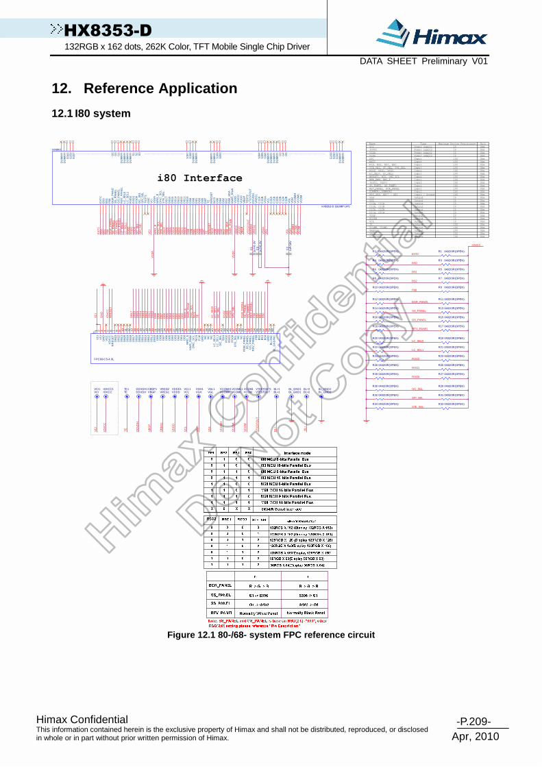
-P.209- Himax Confidential
Apr, 2010
This information contained herein is the exclusive property of Himax and shall not be distributed, reproduced, or disclosed in whole or in part without prior written permission of Himax.
HX8353-D 132RGB x 162 dots, 262K Color, TFT Mobile Single Chip Driver DATA SHEET Preliminary V01
12. Reference Application 12.1 I80 system
R3 0402/0R(OPEN)R4 0402/0R(OPEN)BS0
TEVCOMH, VCOMLVREG1VBGPVTESTOUT 100Output
HIMAX
HX8353-D (BUMP UP)
VC
OM
H
RS
O0
NR
D_E
DN
C_S
CL
ST
E_S
EL
DB
17D
B16
DB
15D
B14
DB
13
VC
OM
GS
_PA
NE
L
G2
DU
MM
Y
G5
G3
S1
S2
S3
S39
6S
395
S39
4
G16
2
G4
G16
1
RE
V_P
AN
EL
VC
OM
L
P68
BS
1B
S0
VC
I
SP
I_S
EL
OS
CT
ES
T1
GC
_SE
L
VS
SA
DU
MM
Y
S19
7S
198
S19
9S
200
BG
R_P
AN
El
SS
_PA
NE
L
DB
11D
B10
DB
9D
B8
DB
1D
B3
DB
5D
B7
TE
NR
ES
ET
NC
SD
B6
DB
4D
B2
BS
2D
B0_
SD
AN
WR
_RN
WV
SS
DIO
VC
CV
DD
DV
BG
PT
ES
T2
VT
ES
TO
UT
DD
VD
HV
RE
G1
C11
AC
11B
VS
SA
VC
LC
21A
C21
BC
22A
C22
BC
12A
VG
LV
GH
RS
O2
RS
O1
LC_S
EL1
EX
TC
DB
12
C12
B
LC_S
EL0
G16
0G
158
G15
9G
157
DU
MM
YD
UM
MY
G6
DU
MM
YD
UM
MY
DU
MM
YD
UM
MY
DU
MM
Y
DU
MM
Y
DU
MM
YD
UM
MY
DU
MM
YD
UM
MY
G1
DU
MM
Y
DU
MM
Y
DB
6N
CS
VTESTOUT1VTESTOUT
NR
ES
ET
TE
DB
7D
B5
DB
3D
B1
DB
8D
B9
DB
10D
B11
DB
12D
B13
DB
14D
B15
RE
V_P
AN
EL
DB
16
GS
_PA
NE
L
DB
17S
TE
_SE
LD
NC
_SC
LN
RD
_E
VC
I
GC
_SE
LR
SO
0R
SO
1R
SO
2
LC_S
EL0
LC_S
EL1
SS
_PA
NE
L
P68
BS
1B
S0
VC
OM
EX
TC
VC
OM
LV
CO
MH
VG
H
BG
R_P
AN
EL
VG
L
SP
I_S
EL
VR
EG
1D
DV
DH
VT
ES
TO
UT
VB
GP
VD
DD
IOV
CC
NW
R_R
NW
DB
0_S
DA
BS
2D
B2
DB
4
IOVCC
VT
ES
TO
UT
OhmOhmOhmOhmOhmOhmOhmOhmOhmOhmOhmOhmOhmOhm
R5 0402/0R(OPEN)R6 0402/0R(OPEN)BS1
R7 0402/0R(OPEN)R8 0402/0R(OPEN)BS2
R9 0402/0R(OPEN)P68
R10 0402/0R(OPEN)
EXTC
R11 0402/0R(OPEN)R12 0402/0R(OPEN)BGR_PANEL
VS
SA
RS
O0
ST
E_S
EL
RG
B_P
AN
EL
SS
_PA
NE
LG
S_P
AN
EL
RE
V_P
AN
EL
IOV
CC
NR
ES
ET
VC
I
GN
D
R13 0402/0R(OPEN)SS_PANEL
BS
2
R14 0402/0R(OPEN)
BS
0B
S1
DB
11
DB
13
NC
S
DB
15
DB
8D
B9
DB
5
DB
12
DB
14
DB
10
DB
4
DB
7D
B6
DB
3
NW
R_R
NW
DB
1
STE_SEL, GC_SEL, SPI_SELRSO0, RSO1, RSO2
DB
2LC_SEL0, LC_SEL1NRESET, NCS, DNC_SCLNWR_RNW, NRD_ETEST2, TEST1
DB
0N
RD
_E
DN
C_S
CL
DB
16D
B17
TE
LC_S
EL0
LC_S
EL1
GC
_SE
L
P68
RS
O2
J2
FPC60-0.5-4.0L
VC
I1
VC
I2
GN
D3
VC
C4
IOV
CC
5
NR
ES
ET
6
DB
1713
DB
1614
DB
1515
DB
1416
DB
1317
DB
1218
DB
1119
DB
1020
DB
921
DB
822
DB
723
DB
624
DB
525
DB
426
DB
327
DB
228
DB
129
DB
030
NR
D_E
31
NW
R_R
NW
32
DN
C_S
CL
33
NC
S34
FLM
35
GN
D36
NC
37
NC
38
NC
39
LC_S
EL0
40
LC_S
EL1
41
GC
_SE
L42
SD
A43
RS
O2
44
RS
O1
45
RS
O0
46
ST
E_S
EL
47
NC
48
NC
49
RG
B_P
AN
EL
50
SS
_PA
NE
L51
GS
_PA
NE
L52
RE
V_P
AN
EL
53
P68
54
BS
255
BS
156
BS
057
GN
D58
BL+
/NC
59
BL_
GN
D/N
C60
DB
237
DB
228
DB
219
DB
2010
DB
1911
DB
1812
SS_PANEL, GS_PANEL
RS
O1
REV_PANEL, BGR_PANELDUMMYR1,DUMMYR2DB0_SDA, DB17 ~ DB1
VS
SD
GS_PANELR15 0402/0R(OPEN)R16 0402/0R(OPEN)
R17 0402/0R(OPEN)REV_PANEL
R18 0402/0R(OPEN)
BL+
DD
VD
H
VC
L
VG
H
VG
L
VR
EG
1
VC
OM
VC
OM
L
VD
DD
VC
OM
H
TE
BL+
VS
SA
VCOM1VCOM
BL+2BL+2
VDDD1VDDD
R19 0402/0R(OPEN)LC_SEL0
R20 0402/0R(OPEN)
DDVDH1DDVDH
VCOMH1VCOMH
TE1TE
VCOML1VCOML
VCL1VCL
VREG2VREG1
VGL1VGL
VGH1VGH
BL+1BL+1
BL_GND1BL_GND1
VC
I
BL_GND2BL_GND2
IOV
CC
VCI1VCI
IOVCC1IOVCC
LC_SEL1R21 0402/0R(OPEN)R22 0402/0R(OPEN)
VBGP1VBGP
RSO2R23 0402/0R(OPEN)R24 0402/0R(OPEN)
R25 0402/0R(OPEN)RSO1
R26 0402/0R(OPEN)
VB
GP
i80 Interface
RSO0R27 0402/0R(OPEN)R28 0402/0R(OPEN)
Name Type
101010101010101010100100
Input / Output
R29 0402/0R(OPEN)GC_SEL
R30 0402/0R(OPEN)
Maximum Series Resistance UnitVCI Power supply 10 Ohm
OhmOhmOhmOhmOhmOhmOhmOhmOhmOhmOhmOhmOhmOhmOhmOhm
IOVCC
R1 0402/0R(OPEN)
Power supply 101010
VSSA Power supplyPower supplyVSSD
OSC InputInputInputInputInputInputInputInputInputInputInputInput
100100100100100100100100100100100100100
EXTCP68, BS2, BS1, BS0
R31 0402/0R(OPEN)R32 0402/0R(OPEN)SPI_SEL
VGH OutputOutputOutputOutputOutputOutputOutputOutputOutputOutputOutputOutputOutput
VGLC11A, C11B
R33 0402/0R(OPEN)R34 0402/0R(OPEN)STE_SEL
C12A, C12B
R2 0402/0R(OPEN)
C22A, C22BC21A, C21BVDDDDDVDHVCL
100
C1
1uF
/6.3
V
100
C2
1uF
/16V
VC
L
C3
1uF
/6.3
V
Figure 12.1 80-/68- system FPC reference circuit

-P.210- Himax Confidential
Apr, 2010
This information contained herein is the exclusive property of Himax and shall not be distributed, reproduced, or disclosed in whole or in part without prior written permission of Himax.
HX8353-D 132RGB x 162 dots, 262K Color, TFT Mobile Single Chip Driver DATA SHEET Preliminary V01
12.2 SPI system
C2
1uF
/6.3
V
C1
1uF
/6.3
V
C3
1uF
/16V
RS
O0
NR
ES
ET
NR
D_E
NC
S
DN
C_S
CL
NW
R_R
NW
VC
L
DD
VD
H
2. The input pin must be fixed IOVCC or GND when no use. Refer to "Pin Description".
VG
L
VG
H
VC
OM
L
VC
OM
VR
EG
1
VD
DD
X
ST
E_S
EL
VC
OM
H
NC
S
OS
C
TE
NR
ES
ET
0
TE
DNC_SCL1DNC_SCL
1
VCOM2VCOM
NCS1NCS
0
BGR_PANEL
VDDD2VDDD
RG
B_P
AN
EL
NWR_RNW1NWR_RNW
SS
_PA
NE
L
X
OS
C
0
GS
_PA
NE
L
1
RE
V_P
AN
EL
VTESTOUT2VTESTOUT
DDVDH2DDVDH
VCOMH2VCOMH
1 X
TE2TE
Himax HX8353-D (BUMP UP)
VC
OM
H
RS
O0
NR
D_E
DN
C_S
CL
ST
E_S
EL
DB
17D
B16
DB
15D
B14
DB
13
VC
OM
GS
_PA
NE
L
G2
DU
MM
Y
G5
G3
S1
S2
S3
S39
6S
395
S39
4
G16
2
G4
G16
1
RE
V_P
AN
EL
VC
OM
L
P68
BS
1B
S0
VC
I
SP
I_S
EL
OS
CT
ES
T1
GC
_SE
L
VS
SA
DU
MM
Y
S19
7S
198
S19
9S
200
BG
R_P
AN
El
SS
_PA
NE
L
DB
11D
B10
DB
9D
B8
DB
1D
B3
DB
5D
B7
TE
NR
ES
ET
NC
SD
B6
DB
4D
B2
BS
2D
B0_
SD
AN
WR
_RN
WV
SS
DIO
VC
CV
DD
DV
BG
PT
ES
T2
VT
ES
TO
UT
DD
VD
HV
RE
G1
C11
AC
11B
VS
SA
VC
LC
21A
C21
BC
22A
C22
BC
12A
VG
LV
GH
RS
O2
RS
O1
LC_S
EL1
EX
TC
DB
12
C12
B
LC_S
EL0
G16
0G
158
G15
9G
157
DU
MM
YD
UM
MY
G6
DU
MM
YD
UM
MY
DU
MM
YD
UM
MY
DU
MM
Y
DU
MM
Y
DU
MM
YD
UM
MY
DU
MM
YD
UM
MY
G1
DU
MM
Y
DU
MM
Y
VB
GP
VCOML2VCOML
VBGP2VBGP
VT
ES
TO
UT
VCL2VCL
GS
_PA
NE
L
NRESET1NRESET
VGL2VGL
NR
ES
ET
IOV
CC
VC
I
NRD_E1NRD_E
VGH2VGH
VREG3VREG1
OSC1OSC
GN
D
ST
E_S
EL
0
DN
C_S
CL
1
IOV
CC
R -> G -> B
VS
SA
SS_PANEL
B -> G -> R
VC
I
GC
_SE
LR
SO
0
GS_PANEL
RS
O1
REV_PANEL
RS
O2
GN
D
01 X
S1 -> S396
0
1
S396 -> S1
SS
_PA
NE
L
0
G1 -> G162 G162 -> G1
1
132RGB X 162 (Display 132RGB X 162)
GRAM Resolution
X
128RGB X 128 (Display 128RGB X 128)
132RGB X 162 (Display 128RGB X 160)
128RGB X 160(Display 128RGB X 160)
120RGB X 160(Display 120RGB X 160)
96RGB X 64(Display 96RGB X 64)
96RGB X 68(Display 96RGB X 68)
Normally White Panel
Note: SS_PANEL and GS_PANEL is base on RSO[2:0]="00 0", otherRSO[2:0] setting please reference "Pin Description"
Normally Black Panel
VC
OM
NW
R_R
NW
NC
ST
EG
ND
DN
C_S
CL
VC
OM
HV
CO
ML
VG
L
BG
R_P
AN
EL
VG
H
VC
L
SP
I_S
EL
VR
EG
1
VS
SA
DD
VD
HV
TE
ST
OU
T
RSO0RSO1RSO2 STE_SEL
00 00
00
VB
GP
10
VD
DD
VS
SD
IOV
CC
NW
R_R
NW
GND3GND
GND4GND
DB
0_S
DA
J3
FPC60-0.5-4.0L
VC
I1
VC
I2
GN
D3
VC
C4
IOV
CC
5
NR
ES
ET
6
DB
1713
DB
1614
DB
1515
DB
1416
DB
1317
DB
1218
DB
1119
DB
1020
DB
921
DB
822
DB
723
DB
624
DB
525
DB
426
DB
327
DB
228
DB
129
DB
030
NR
D_E
31
NW
R_R
NW
32
DN
C_S
CL
33
NC
S34
FLM
35
GN
D36
NC
37
NC
38
LC_S
EL0
39
LC_S
EL1
40
GC
_SE
L41
SP
I_S
EL
42
SD
A43
RS
O2
44
RS
O1
45
RS
O0
46
ST
E_S
EL
47
NC
48
NC
49
RG
B_P
AN
EL
50
SS
_PA
NE
L51
GS
_PA
NE
L52
RE
V_P
AN
EL
53
P68
54
BS
255
BS
156
BS
057
GN
D58
BL+
/NC
59
BL_
GN
D/N
C60
DB
237
DB
228
DB
219
DB
2010
DB
1911
DB
1812
RS
O2
VC
I
0
IOV
CC
0
1. VCI, IOVCC are separated from different power so urce to get better display quality.
VCI2VCI
RS
O1
IOVCC2IOVCC
DB
0_S
DA SPI_SEL: "0":3-Wire ; "1":4-Wire
1
LC_S
EL0
EX
TC
LC_S
EL1
RE
V_P
AN
EL
LC_S
EL1
LC_S
EL0
SP
I_S
EL
GC
_SE
L
IOVCC
EXTC
R4 0402/0R(OPEN)BGR_PANEL
R3 0402/0R(OPEN)
R6 0402/0R(OPEN)SS_PANEL
R5 0402/0R(OPEN)
R8 0402/0R(OPEN)GS_PANEL
R7 0402/0R(OPEN)
R10 0402/0R(OPEN)REV_PANEL
R9 0402/0R(OPEN)
LC_SEL0R12 0402/0R(OPEN)R11 0402/0R(OPEN)
R14 0402/0R(OPEN)LC_SEL1
R13 0402/0R(OPEN)
RSO2R16 0402/0R(OPEN)R15 0402/0R(OPEN)
R18 0402/0R(OPEN)RSO1
R17 0402/0R(OPEN)
RSO0R20 0402/0R(OPEN)R19 0402/0R(OPEN)
R22 0402/0R(OPEN)R21 0402/0R(OPEN)GC_SEL
R2 0402/0R(OPEN)
R24 0402/0R(OPEN)SPI_SEL
R23 0402/0R(OPEN)
R26 0402/0R(OPEN)STE_SEL
R25 0402/0R(OPEN)
R1 0402/0R(OPEN)
SPI Interface
Figure 12.2 SPI FPC reference circuit

-P.211- Himax Confidential
Apr, 2010
This information contained herein is the exclusive property of Himax and shall not be distributed, reproduced, or disclosed in whole or in part without prior written permission of Himax.
HX8353-D 132RGB x 162 dots, 262K Color, TFT Mobile Single Chip Driver DATA SHEET Preliminary V01
12.3 1st Pixel is at right-bottom of the panel & RGB filter order = RGB
00H
Driver IC (Bump down)
G161
G3
G160
G2S7 S390
00H 01H 02H ----------------------------------------------------------------------------------- 7DH 7EH 7FH
G1
G3
|
|
|
|
|
|
|
|
|
|
|
|
|
|
|
|
|
|
|
|
|
|
|
|
|
|
|
|
|
|
|
|
|
G157
G159
G2
G4
|
|
|
|
|
|
|
|
|
|
|
|
|
|
|
|
|
|
|
|
|
|
|
|
|
|
|
|
|
|
|
|
|
G158
G160
1st Pixel
Direction default setting (H/W)
SMX = 1
SMY = 1
SRGB = 0
S1 = Filter B
S2 = Filter G
S3 = Filter R
Display direction control (S/W)
X – Mirror control by MX
Y – Mirror control by MY
XY – Exchange control by MV

-P.212- Himax Confidential
Apr, 2010
This information contained herein is the exclusive property of Himax and shall not be distributed, reproduced, or disclosed in whole or in part without prior written permission of Himax.
HX8353-D 132RGB x 162 dots, 262K Color, TFT Mobile Single Chip Driver DATA SHEET Preliminary V01
12.4 1st Pixel is at left-top of the panel & RGB filter ord er = BGR
00H
Driver IC (Bump down)
G161
G3
G160
G2S7 S390
00H 01H 02H ----------------------------------------------------------------------------------- 7DH 7EH 7FH
G1
G3
|
|
|
|
|
|
|
|
|
|
|
|
|
|
|
|
|
|
|
|
|
|
|
|
|
|
|
|
|
|
|
|
|
G157
G159
G2
G4
|
|
|
|
|
|
|
|
|
|
|
|
|
|
|
|
|
|
|
|
|
|
|
|
|
|
|
|
|
|
|
|
|
G158
G160
1st Pixel
Direction default setting (H/W)
SMX = 0
SMY = 0
SRGB = 1
S1 = Filter B
S2 = Filter G
S3 = Filter R
Display direction control (S/W)
X – Mirror control by MX
Y – Mirror control by MY
XY – Exchange control by MV

-P.213- Himax Confidential
Apr, 2010
This information contained herein is the exclusive property of Himax and shall not be distributed, reproduced, or disclosed in whole or in part without prior written permission of Himax.
HX8353-D 132RGB x 162 dots, 262K Color, TFT Mobile Single Chip Driver DATA SHEET Preliminary V01
12.5 Application of connection with Different reso lution
Case 1 of resolution (128RGB x 160) (RSO[2:0] = 011) RAM size = 128 x 160 x 18-bits (Used) Display size = 128RGB x 160 Example for SMX = SMY = 0

-P.214- Himax Confidential
Apr, 2010
This information contained herein is the exclusive property of Himax and shall not be distributed, reproduced, or disclosed in whole or in part without prior written permission of Himax.
HX8353-D 132RGB x 162 dots, 262K Color, TFT Mobile Single Chip Driver DATA SHEET Preliminary V01
Example for SMX = SMY = 1

-P.215- Himax Confidential
Apr, 2010
This information contained herein is the exclusive property of Himax and shall not be distributed, reproduced, or disclosed in whole or in part without prior written permission of Himax.
HX8353-D 132RGB x 162 dots, 262K Color, TFT Mobile Single Chip Driver DATA SHEET Preliminary V01
Case 2 of resolution (120RGB x 160) (RSO[2:0] = 010) RAM size = 120 x 160 x 18-bits (Used) Display size = 120RGB x 160
Example for SMX = SMY = 0

-P.216- Himax Confidential
Apr, 2010
This information contained herein is the exclusive property of Himax and shall not be distributed, reproduced, or disclosed in whole or in part without prior written permission of Himax.
HX8353-D 132RGB x 162 dots, 262K Color, TFT Mobile Single Chip Driver DATA SHEET Preliminary V01
Example for SMX = SMY = 1
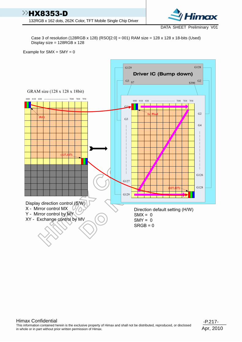
-P.217- Himax Confidential
Apr, 2010
This information contained herein is the exclusive property of Himax and shall not be distributed, reproduced, or disclosed in whole or in part without prior written permission of Himax.
HX8353-D 132RGB x 162 dots, 262K Color, TFT Mobile Single Chip Driver DATA SHEET Preliminary V01
Case 3 of resolution (128RGB x 128) (RSO[2:0] = 001) RAM size = 128 x 128 x 18-bits (Used) Display size = 128RGB x 128
Example for SMX = SMY = 0
00H
Driver IC (Bump down)
G129
G3
G128
G2S7 S390
00H 01H 02H -------------------------------- 7DH 7EH 7FH
G1
G3
|
|
|
|
|
|
|
|
|
|
|
|
|
|
G127
G129
G2
G4
|
|
|
|
|
|
|
|
|
|
|
G126
G128
1st Pixel
00H 01H 02H -------------------------------- 7DH 7EH 7FH
(0,0)
(127,127)
GRAM size (128 x 128 x 18bit)
Display direction control (S/W)
X - Mirror control MX
Y - Mirror control by MY
XY - Exchange control by MV
Direction default setting (H/W)
SMX = 0
SMY = 0
SRGB = 0
(127,127)

-P.218- Himax Confidential
Apr, 2010
This information contained herein is the exclusive property of Himax and shall not be distributed, reproduced, or disclosed in whole or in part without prior written permission of Himax.
HX8353-D 132RGB x 162 dots, 262K Color, TFT Mobile Single Chip Driver DATA SHEET Preliminary V01
Example for SMX = SMY = 1
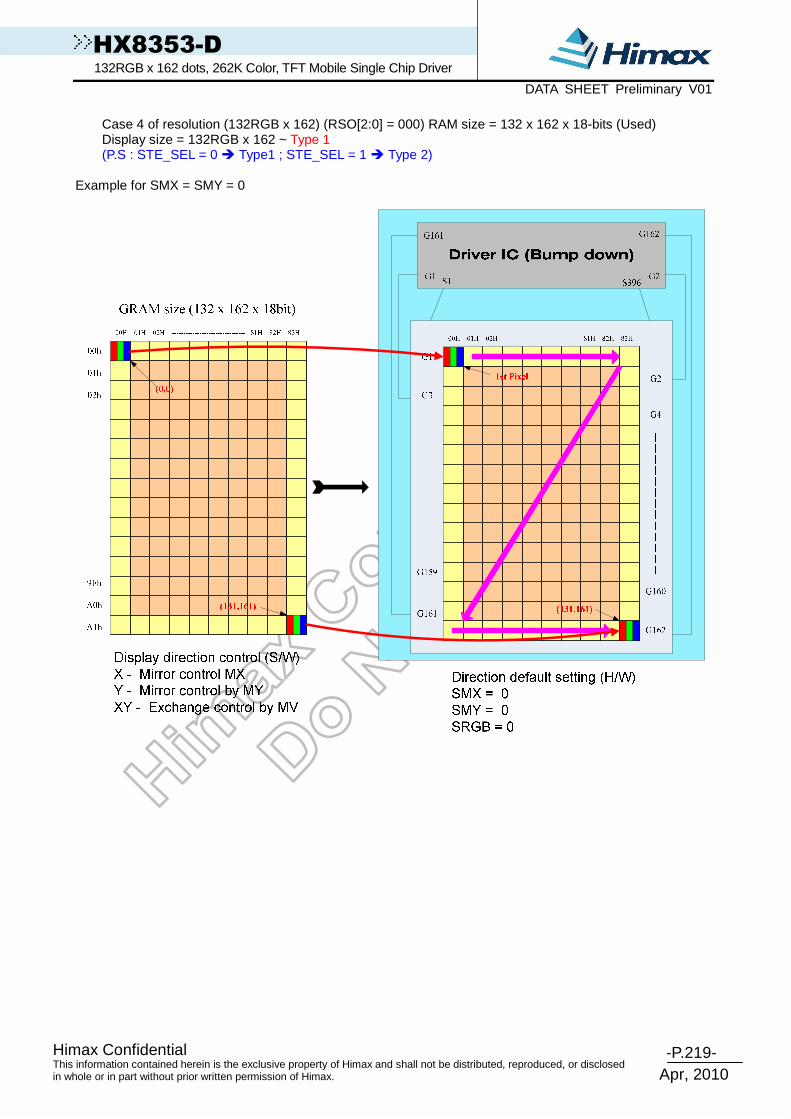
-P.219- Himax Confidential
Apr, 2010
This information contained herein is the exclusive property of Himax and shall not be distributed, reproduced, or disclosed in whole or in part without prior written permission of Himax.
HX8353-D 132RGB x 162 dots, 262K Color, TFT Mobile Single Chip Driver DATA SHEET Preliminary V01
Case 4 of resolution (132RGB x 162) (RSO[2:0] = 000) RAM size = 132 x 162 x 18-bits (Used) Display size = 132RGB x 162 ~ Type 1 (P.S : STE_SEL = 0 Type1 ; STE_SEL = 1 Type 2)
Example for SMX = SMY = 0

-P.220- Himax Confidential
Apr, 2010
This information contained herein is the exclusive property of Himax and shall not be distributed, reproduced, or disclosed in whole or in part without prior written permission of Himax.
HX8353-D 132RGB x 162 dots, 262K Color, TFT Mobile Single Chip Driver DATA SHEET Preliminary V01
Example for SMX = SMY = 1

-P.221- Himax Confidential
Apr, 2010
This information contained herein is the exclusive property of Himax and shall not be distributed, reproduced, or disclosed in whole or in part without prior written permission of Himax.
HX8353-D 132RGB x 162 dots, 262K Color, TFT Mobile Single Chip Driver DATA SHEET Preliminary V01
Display size = 132RGB x 162 ~ Type 2 (P.S : STE_SEL = 0 Type1 ; STE_SEL = 1 Type 2)
Example for SMX = SMY = 0
00H
Driver IC (Bump down)
G161
G3
G160
G2S7 S390
00H 01H 02H -------------------------------- 7DH 7EH 7FH
G1
G3
|
|
|
|
|
|
|
|
|
|
|
|
|
|
G159
G161
G2
G4
|
|
|
|
|
|
|
|
|
|
|
G158
G160
1st Pixel
00H 01H 02H -------------------------------- 7DH 7EH 7FH
(0,0)
(131,161)
GRAM size (132 x 162 x 18bit)
Display direction control (S/W)
X - Mirror control MX
Y - Mirror control by MY
XY - Exchange control by MV
Direction default setting (H/W)
SMX = 0
SMY = 0
SRGB = 0
(127,159)
(2,1)
(129,160)
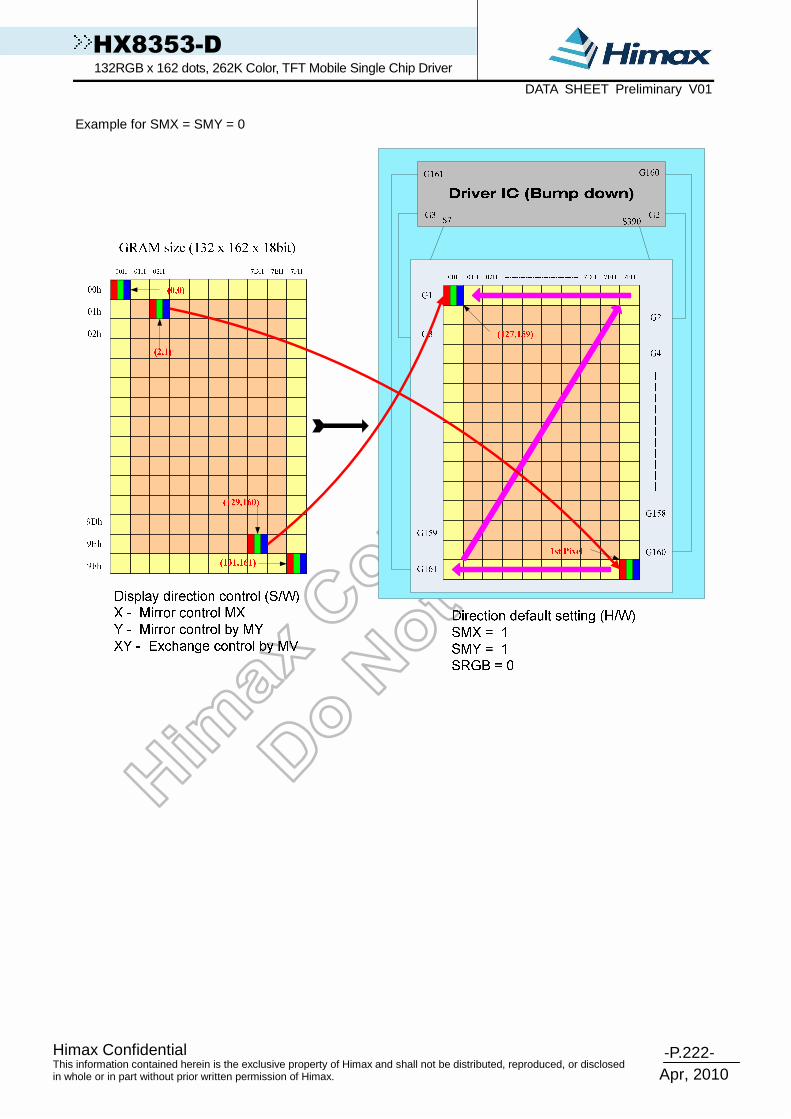
-P.222- Himax Confidential
Apr, 2010
This information contained herein is the exclusive property of Himax and shall not be distributed, reproduced, or disclosed in whole or in part without prior written permission of Himax.
HX8353-D 132RGB x 162 dots, 262K Color, TFT Mobile Single Chip Driver DATA SHEET Preliminary V01
Example for SMX = SMY = 0

-P.223- Himax Confidential
Apr, 2010
This information contained herein is the exclusive property of Himax and shall not be distributed, reproduced, or disclosed in whole or in part without prior written permission of Himax.
HX8353-D 132RGB x 162 dots, 262K Color, TFT Mobile Single Chip Driver DATA SHEET Preliminary V01
Case 5 of resolution (96RGB x 68) (RSO[2:0] = 100) RAM size = 96 x 68 x 18-bits (Used) Display size = 96RGB x 68
Example for SMX = SMY = 0

-P.224- Himax Confidential
Apr, 2010
This information contained herein is the exclusive property of Himax and shall not be distributed, reproduced, or disclosed in whole or in part without prior written permission of Himax.
HX8353-D 132RGB x 162 dots, 262K Color, TFT Mobile Single Chip Driver DATA SHEET Preliminary V01
Example for SMX = SMY = 1

-P.225- Himax Confidential
Apr, 2010
This information contained herein is the exclusive property of Himax and shall not be distributed, reproduced, or disclosed in whole or in part without prior written permission of Himax.
HX8353-D 132RGB x 162 dots, 262K Color, TFT Mobile Single Chip Driver DATA SHEET Preliminary V01
Case 6 of resolution (96RGB x 64) (RSO[2:0] = 101) RAM size = 96 x 64 x 18-bits (Used) Display size = 96RGB x 64
Example for SMX = SMY = 0
00H
Driver IC (Bump down)
G63
G1
G64
G2S55 S342
00H 01H 02H -------------------------------- 7DH 7EH 7FH
G1
G3
|
|
|
|
|
|
|
|
|
|
|
|
G61
G63
G2
G4
|
|
|
|
|
|
|
|
|
|
|
|
G62
G64
1st Pixel
00H 01H 02H -------------------------------- 5DH 5EH 5FH
(0,0)
(95,63)
GRAM size (96 x 64 x 18bit)
Display direction control (S/W)
X - Mirror control MX
Y - Mirror control by MY
XY - Exchange control by MV
Direction default setting (H/W)
SMX = 0
SMY = 0
SRGB = 0
(95,63)
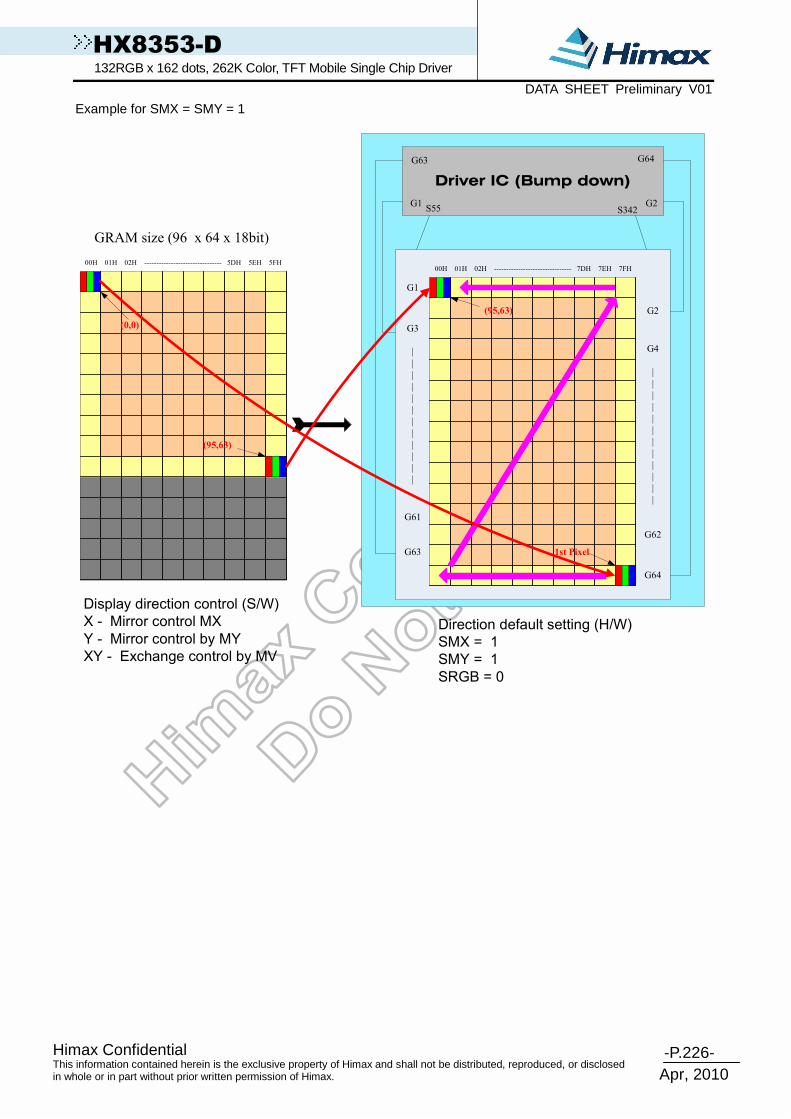
-P.226- Himax Confidential
Apr, 2010
This information contained herein is the exclusive property of Himax and shall not be distributed, reproduced, or disclosed in whole or in part without prior written permission of Himax.
HX8353-D 132RGB x 162 dots, 262K Color, TFT Mobile Single Chip Driver DATA SHEET Preliminary V01
Example for SMX = SMY = 1
00H
Driver IC (Bump down)
G63
G1
G64
G2S55 S342
00H 01H 02H -------------------------------- 7DH 7EH 7FH
G1
G3
|
|
|
|
|
|
|
|
|
|
|
|
G61
G63
G2
G4
|
|
|
|
|
|
|
|
|
|
|
|
G62
G64
1st Pixel
00H 01H 02H -------------------------------- 5DH 5EH 5FH
(0,0)
(95,63)
GRAM size (96 x 64 x 18bit)
Display direction control (S/W)
X - Mirror control MX
Y - Mirror control by MY
XY - Exchange control by MV
Direction default setting (H/W)
SMX = 1
SMY = 1
SRGB = 0
(95,63)

-P.227- Himax Confidential
Apr, 2010
This information contained herein is the exclusive property of Himax and shall not be distributed, reproduced, or disclosed in whole or in part without prior written permission of Himax.
HX8353-D 132RGB x 162 dots, 262K Color, TFT Mobile Single Chip Driver DATA SHEET Preliminary V01
13. Ordering Information
Part No. Package
HX8353-D000 PDxxx PD : mean COG xxx : mean chip thickness (µm), (default: 250 µm)
14. Revision History
Version Date Description of Changes 2009/02/25 New setup 2009/03/27 Remove VPNL_EN in P.166 2009/04/20 Add In-House Register Command Setting 2009/04/23 Modify RB5H => VR_TRIM(From [5:0] to [3:0]) 2009/05/25 Remove B1H Blank FS1[3:0] & FS0[3:0] 2009/05/25 Modify B1H => PON is control VCL and VGL on/off 2009/05/25 Modify BFH => PTBA[15] is control VGH on/off 2009/06/17 Add application of connection with Different resolution
2009/06/29
Modify VCI voltage form 2.3V to 2.5V Modify In-house register function. Modify OTP table. Modify Chip Size and pad coordinates. Modify CAP application (1uF at DDVDH, VGL, C11)
2009/08/06 New Setup HX8353D ES1.0 2009/08/12 Modify C1:16V 6.3V ; C2:16V 6.3V 2009/09/02 Modify Au Bump Height 15um 12um 2009/11/02 Modify ES1.3 IC default value 2009/12/21 Modify OTP_index table and the N_RTN default value. 2009/12/23 Modify chip thickness from 300um to 250um 2010/01/22 Modify Pin assignment 2010/02/02 update VGH & VGL voltage spec (P7,P11,P166) 2010/02/09 Modify Fosc setting table 2010/02/10 Define OTP current limit ≧20mA
2010/04/12 Add VMF setting Note2(When Setting the VMF, be careful the VCOMH & VCOML voltage’s range.)
01
2010/04/23 Add RB0H、RC0H、RCBH、RE3H Register Command Set


