Embed Size (px)
Citation preview
REV. A
Information furnished by Analog Devices is believed to be accurate andreliable. However, no responsibility is assumed by Analog Devices for itsuse, nor for any infringements of patents or other rights of third partieswhich may result from its use. No license is granted by implication orotherwise under any patent or patent rights of Analog Devices.
aAD7705/AD7706
One Technology Way, P.O. Box 9106, Norwood, MA 02062-9106, U.S.A.
Tel: 781/329-4700 World Wide Web Site: http://www.analog.com
Fax: 781/326-8703 © Analog Devices, Inc., 1998
3 V/5 V, 1 mW2-/3-Channel 16-Bit, Sigma-Delta ADCs
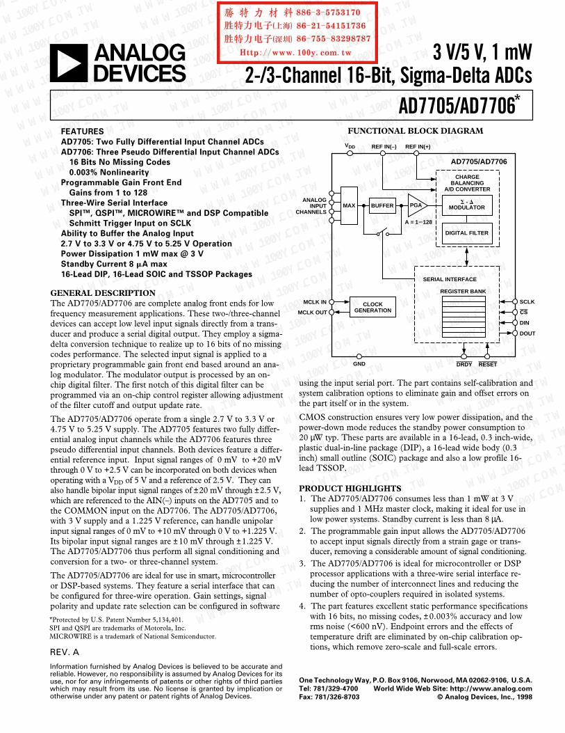
FUNCTIONAL BLOCK DIAGRAMFEATURES
AD7705: Two Fully Differential Input Channel ADCs
AD7706: Three Pseudo Differential Input Channel ADCs
16 Bits No Missing Codes
0.003% Nonlinearity
Programmable Gain Front End
Gains from 1 to 128
Three-Wire Serial Interface
SPI™, QSPI™, MICROWIRE™ and DSP Compatible
Schmitt Trigger Input on SCLK
Ability to Buffer the Analog Input
2.7 V to 3.3 V or 4.75 V to 5.25 V Operation
Power Dissipation 1 mW max @ 3 V
Standby Current 8 mA max
16-Lead DIP, 16-Lead SOIC and TSSOP Packages
GENERAL DESCRIPTIONThe AD7705/AD7706 are complete analog front ends for lowfrequency measurement applications. These two-/three-channeldevices can accept low level input signals directly from a trans-ducer and produce a serial digital output. They employ a sigma-delta conversion technique to realize up to 16 bits of no missingcodes performance. The selected input signal is applied to aproprietary programmable gain front end based around an ana-log modulator. The modulator output is processed by an on-chip digital filter. The first notch of this digital filter can beprogrammed via an on-chip control register allowing adjustmentof the filter cutoff and output update rate.
The AD7705/AD7706 operate from a single 2.7 V to 3.3 V or4.75 V to 5.25 V supply. The AD7705 features two fully differ-ential analog input channels while the AD7706 features threepseudo differential input channels. Both devices feature a differ-ential reference input. Input signal ranges of 0 mV to +20 mVthrough 0 V to +2.5 V can be incorporated on both devices whenoperating with a VDD of 5 V and a reference of 2.5 V. They canalso handle bipolar input signal ranges of ±20 mV through ±2.5 V,which are referenced to the AIN(–) inputs on the AD7705 and tothe COMMON input on the AD7706. The AD7705/AD7706,with 3 V supply and a 1.225 V reference, can handle unipolarinput signal ranges of 0 mV to +10 mV through 0 V to +1.225 V.Its bipolar input signal ranges are ±10 mV through ±1.225 V.The AD7705/AD7706 thus perform all signal conditioning andconversion for a two- or three-channel system.
The AD7705/AD7706 are ideal for use in smart, microcontrolleror DSP-based systems. They feature a serial interface that canbe configured for three-wire operation. Gain settings, signalpolarity and update rate selection can be configured in software
using the input serial port. The part contains self-calibration andsystem calibration options to eliminate gain and offset errors onthe part itself or in the system.
CMOS construction ensures very low power dissipation, and thepower-down mode reduces the standby power consumption to20 µW typ. These parts are available in a 16-lead, 0.3 inch-wide,plastic dual-in-line package (DIP), a 16-lead wide body (0.3inch) small outline (SOIC) package and also a low profile 16-lead TSSOP.
PRODUCT HIGHLIGHTS1. The AD7705/AD7706 consumes less than 1 mW at 3 V
supplies and 1 MHz master clock, making it ideal for use inlow power systems. Standby current is less than 8 µA.
2. The programmable gain input allows the AD7705/AD7706to accept input signals directly from a strain gage or trans-ducer, removing a considerable amount of signal conditioning.
3. The AD7705/AD7706 is ideal for microcontroller or DSPprocessor applications with a three-wire serial interface re-ducing the number of interconnect lines and reducing thenumber of opto-couplers required in isolated systems.
4. The part features excellent static performance specificationswith 16 bits, no missing codes, ±0.003% accuracy and lowrms noise (<600 nV). Endpoint errors and the effects oftemperature drift are eliminated by on-chip calibration op-tions, which remove zero-scale and full-scale errors.
*
*Protected by U.S. Patent Number 5,134,401.SPI and QSPI are trademarks of Motorola, Inc.MICROWIRE is a trademark of National Semiconductor.
VDD REF IN(–) REF IN(+)
AD7705/AD7706
MAX PGABUFFER
CHARGEBALANCING
A/D CONVERTER
S - DMODULATOR
DIGITAL FILTER
A = 1<128
SERIAL INTERFACE
REGISTER BANK
CLOCKGENERATION
MCLK IN
MCLK OUT
GND DRDY RESET
DIN
DOUT
CS
SCLK
ANALOGINPUT
CHANNELS
–2– REV. A
AD7705/AD7706–SPECIFICATIONS (VDD = +3 V or 5 V, REF IN(+) = +1.225 V with VDD = 3 V and +2.5 Vwith VDD = 5 V; REF IN(–) = GND; MCLK IN = 2.4576 MHz unless otherwise noted. All specifications TMIN to TMAX unless otherwise noted.)
Parameter B Version1 Units Conditions/Comments
STATIC PERFORMANCENo Missing Codes 16 Bits min Guaranteed by Design. Filter Notch < 60 HzOutput Noise See Tables I and III Depends on Filter Cutoffs and Selected GainIntegral Nonlinearity2 ±0.003 % of FSR max Filter Notch < 60 Hz. Typically ±0.0003%Unipolar Offset Error See Note 3Unipolar Offset Drift4 0.5 µV/°C typBipolar Zero Error See Note 3Bipolar Zero Drift4 0.5 µV/°C typ For Gains 1, 2 and 4
0.1 µV/°C typ For Gains 8, 16, 32, 64 and 128Positive Full-Scale Error5 See Note 3Full-Scale Drift4, 6 0.5 µV/°C typGain Error7 See Note 3Gain Drift4, 8 0.5 ppm of FSR/°C typBipolar Negative Full-Scale Error2 ±0.003 % of FSR typ Typically ±0.001%Bipolar Negative Full-Scale Drift4 1 µV/°C typ For Gains of 1 to 4
0.6 µV/°C typ For Gains of 8 to 128
ANALOG INPUTS/REFERENCE INPUTS Specifications for AIN and REF IN Unless NotedInput Common-Mode Rejection (CMR)2
VDD = 5 VGain = 1 96 dB typGain = 2 105 dB typGain = 4 110 dB typGain = 8v128 130 dB typ
VDD = 3 VGain = 1 105 dB typGain = 2 110 dB typGain = 4 120 dB typGain = 8v128 130 dB typ
Normal-Mode 50 Hz Rejection2 98 dB typ For Filter Notches of 25 Hz, 50 Hz, ±0.02 × fNOTCHNormal-Mode 60 Hz Rejection2 98 dB typ For Filter Notches of 20 Hz, 60 Hz, ±0.02 × fNOTCHCommon-Mode 50 Hz Rejection2 150 dB typ For Filter Notches of 25 Hz, 50 Hz, ±0.02 × fNOTCH
Common-Mode 60 Hz Rejection2 150 dB typ For Filter Notches of 20 Hz, 60 Hz, ±0.02 × fNOTCHAbsolute/Common-Mode REF IN Voltage2 GND to VDD V min to V maxAbsolute/Common-Mode AIN Voltage2, 9 GND – 30 mV V min BUF Bit of Setup Register = 0
VDD + 30 mV V maxAbsolute/Common-Mode AIN Voltage2, 9 GND + 50 mV V min BUF Bit of Setup Register = 1
VDD – 1.5 V V maxAIN DC Input Current2 1 nA maxAIN Sampling Capacitance2 10 pF maxAIN Differential Voltage Range10 0 to +VREF/GAIN11 nom Unipolar Input Range (B/U Bit of Setup Register = 1)
±VREF/GAIN nom Bipolar Input Range (B/U Bit of Setup Register = 0)AIN Input Sampling Rate, fS GAIN × fCLKIN/64 For Gains of 1 to 4
fCLKIN/8 For Gains of 8 to 128Reference Input Range
REF IN(+) – REF IN(–) Voltage 1/1.75 V min/max VDD = 2.7 V to 3.3 V. VREF = 1.225 ± 1% for SpecifiedPerformance
REF IN(+) – REF IN(–) Voltage 1/3.5 V min/max VDD = 4.75 V to 5.25 V. VREF = 2.5 ± 1% for SpecifiedPerformance
REF IN Input Sampling Rate, fS fCLKIN/64
LOGIC INPUTSInput Current
All Inputs Except MCLK IN ±1 µA max Typically ±20 nAMCLK ±10 µA max Typically ±2 µA
All Inputs Except SCLK and MCLK INVINL, Input Low Voltage 0.8 V max VDD = 5 V
0.4 V max VDD = 3 VVINH, Input High Voltage 2.0 V min VDD = 3 V and 5 V
SCLK Only (Schmitt Triggered Input) VDD = 5 V NOMINALVT+ 1.4/3 V min/V maxVT– 0.8/1.4 V min/V maxVT+ – VT– 0.4/0.8 V min/V max
SCLK Only (Schmitt Triggered Input) VDD = 3 V NOMINALVT+ 1/2.5 V min/V maxVT– 0.4/1.1 V min/V maxVT+ – VT– 0.375/0.8 V min/V max
MCLK IN Only VDD = 5 V NOMINALVINL, Input Low Voltage 0.8 V maxVINH, Input High Voltage 3.5 V min
MCLK IN Only VDD = 3 V NOMINALVINL, Input Low Voltage 0.4 V maxVINH, Input High Voltage 2.5 V min
–3–REV. A
AD7705/AD7706Parameter B Version1 Units Conditions/Comments
LOGIC OUTPUTS (Including MCLK OUT)VOL, Output Low Voltage 0.4 V max ISINK = 800 µA Except for MCLK OUT.12 VDD = 5 V.VOL, Output Low Voltage 0.4 V max ISINK = 100 µA Except for MCLK OUT.12 VDD = 3 V.VOH, Output High Voltage 4 V min ISOURCE = 200 µA Except for MCLK OUT.12 VDD = 5 V.VOH, Output High Voltage VDD–0.6 V min ISOURCE = 100 µA Except for MCLK OUT.12 VDD = 3 V.Floating State Leakage Current ±10 µA maxFloating State Output Capacitance13 9 pF typData Output Coding Binary Unipolar Mode
Offset Binary Bipolar Mode
SYSTEM CALIBRATIONPositive Full-Scale Calibration Limit14 (1.05 × VREF)/GAIN V max GAIN Is the Selected PGA Gain (1 to 128)Negative Full-Scale Calibration Limit14 –(1.05 × VREF)/GAIN V max GAIN Is the Selected PGA Gain (1 to 128)Offset Calibration Limit14 –(1.05 × VREF)/GAIN V max GAIN Is the Selected PGA Gain (1 to 128)Input Span15 (0.8 × VREF)/GAIN V min GAIN Is the Selected PGA Gain (1 to 128)
(2.1 × VREF)/GAIN V max GAIN Is the Selected PGA Gain (1 to 128)
POWER REQUIREMENTSVDD Voltage +2.7 to +3.3 V min to V max For Specified Performance
Power Supply Currents16 Digital I/Ps = 0 V or VDD. External MCLK IN andCLK DIS = 1
0.32 mA max BUF Bit = 0. fCLKIN = 1 MHz. Gains of 1 to 1280.6 mA max BUF Bit = 1. fCLKIN = 1 MHz. Gains of 1 to 1280.4 mA max BUF Bit = 0. fCLKIN = 2.4576 MHz. Gains of 1 to 40.6 mA max BUF Bit = 0. fCLKIN = 2.4576 MHz. Gains of 8 to 1280.7 mA max BUF Bit = 1. fCLKIN = 2.4576 MHz. Gains of 1 to 41.1 mA max BUF Bit = 1. fCLKIN = 2.4576 MHz. Gains of 8 to 128
VDD Voltage +4.75 to +5.25 V min to V max For Specified PerformancePower Supply Currents16 Digital I/Ps = 0 V or VDD. External MCLK IN and
CLK DIS = 1.0.45 mA max BUF Bit = 0. fCLKIN = 1 MHz. Gains of 1 to 1280.7 mA max BUF Bit = 1. fCLKIN = 1 MHz. Gains of 1 to 1280.6 mA max BUF Bit = 0. fCLKIN = 2.4576 MHz. Gains of 1 to 40.85 mA max BUF Bit = 0. fCLKIN = 2.4576 MHz. Gains of 8 to 1280.9 mA max BUF Bit = 1. fCLKIN = 2.4576 MHz. Gains of 1 to 41.3 mA max BUF Bit = 1. fCLKIN = 2.4576 MHz. Gains of 8 to 128
Standby (Power-Down) Current17 16 µA max External MCLK IN = 0 V or VDD. VDD = 5 V. See Figure 98 µA max External MCLK IN = 0 V or VDD. VDD = 3 V
Power Supply Rejection18 See Note 19 dB typ
NOTES1Temperature range as follows: B Version, –40°C to +85°C.2These numbers are established from characterization or design at initial product release.3A calibration is effectively a conversion so these errors will be of the order of the conversion noise shown in Tables I and III. This applies after calibration at thetemperature of interest.
4Recalibration at any temperature will remove these drift errors.5Positive Full-Scale Error includes Zero-Scale Errors (Unipolar Offset Error or Bipolar Zero Error) and applies to both unipolar and bipolar input ranges.6Full-Scale Drift includes Zero-Scale Drift (Unipolar Offset Drift or Bipolar Zero Drift) and applies to both unipolar and bipolar input ranges.7Gain Error does not include Zero-Scale Errors. It is calculated as Full-Scale Error–Unipolar Offset Error for unipolar ranges and Full-Scale Error–Bipolar Zero Error forbipolar ranges.
8Gain Error Drift does not include Unipolar Offset Drift/Bipolar Zero Drift. It is effectively the drift of the part if zero scale calibrations only were performed.9This common-mode voltage range is allowed provided that the input voltage on analog inputs does not go more positive than VDD + 30 mV or go more negative thanGND – 30 mV. Parts are functional with voltages down to GND – 200 mV, but with increased leakage at high temperature.
10The analog input voltage range on AIN(+) is given here with respect to the voltage on AIN(–) on the AD7705 and is given with respect to the COMMON input on theAD7706. The absolute voltage on the analog inputs should not go more positive than VDD + 30 mV, or go more negative than GND – 30 mV for specified performance, inputvoltages of GND – 200 mV can be accommodated, but with increased leakage at high temperature.
11VREF = REF IN(+) – REF IN(–).12These logic output levels apply to the MCLK OUT only when it is loaded with one CMOS load.13Sample tested at +25°C to ensure compliance.14After calibration, if the analog input exceeds positive full scale, the converter will output all 1s. If the analog input is less than negative full scale, the device will output all 0s.15These calibration and span limits apply provided the absolute voltage on the analog inputs does not exceed VDD + 30 mV or go more negative than GND – 30 mV. The offset
calibration limit applies to both the unipolar zero point and the bipolar zero point.16When using a crystal or ceramic resonator across the MCLK pins as the clock source for the device, the VDD current and power dissipation will vary depending on the crystal or
resonator type (see Clocking and Oscillator Circuit section).17If the external master clock continues to run in standby mode, the standby current increases to 150 µA typical at 5 V and 75 µA at 3 V. When using a crystal or ceramic
resonator across the MCLK pins as the clock source for the device, the internal oscillator continues to run in standby mode and the power dissipation depends on the crystalor resonator type (see Standby Mode section).
18Measured at dc and applies in the selected passband. PSRR at 50 Hz will exceed 120 dB with filter notches of 25 Hz or 50 Hz. PSRR at 60 Hz will exceed 120 dB with filternotches of 20 Hz or 60 Hz.
19PSRR depends on both gain and VDD.
Gain 1 2 4 8–128VDD = 3 V 86 78 85 93VDD = 5 V 90 78 84 91
Specifications subject to change without notice.
AD7705/AD7706
–4– REV. A
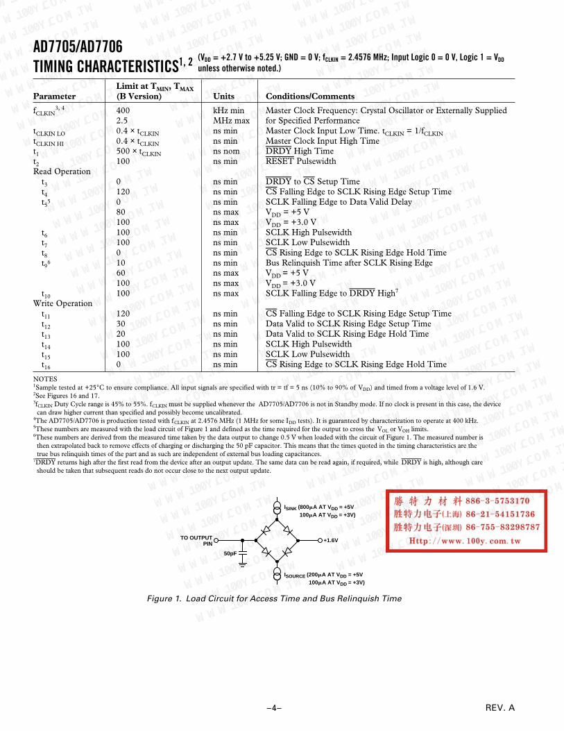
TIMING CHARACTERISTICS1, 2
Limit at TMIN, TMAXParameter (B Version) Units Conditions/Comments
fCLKIN3, 4 400 kHz min Master Clock Frequency: Crystal Oscillator or Externally Supplied
2.5 MHz max for Specified PerformancetCLKIN LO 0.4 × tCLKIN ns min Master Clock Input Low Time. tCLKIN = 1/fCLKINtCLKIN HI 0.4 × tCLKIN ns min Master Clock Input High Timet1 500 × tCLKIN ns nom DRDY High Timet2 100 ns min RESET PulsewidthRead Operation
t3 0 ns min DRDY to CS Setup Timet4 120 ns min CS Falling Edge to SCLK Rising Edge Setup Timet5
5 0 ns min SCLK Falling Edge to Data Valid Delay80 ns max VDD = +5 V100 ns max VDD = +3.0 V
t6 100 ns min SCLK High Pulsewidtht7 100 ns min SCLK Low Pulsewidtht8 0 ns min CS Rising Edge to SCLK Rising Edge Hold Timet9
6 10 ns min Bus Relinquish Time after SCLK Rising Edge60 ns max VDD = +5 V100 ns max VDD = +3.0 V
t10 100 ns max SCLK Falling Edge to DRDY High7
Write Operationt11 120 ns min CS Falling Edge to SCLK Rising Edge Setup Timet12 30 ns min Data Valid to SCLK Rising Edge Setup Timet13 20 ns min Data Valid to SCLK Rising Edge Hold Timet14 100 ns min SCLK High Pulsewidtht15 100 ns min SCLK Low Pulsewidtht16 0 ns min CS Rising Edge to SCLK Rising Edge Hold Time
NOTES1Sample tested at +25°C to ensure compliance. All input signals are specified with tr = tf = 5 ns (10% to 90% of VDD) and timed from a voltage level of 1.6 V.2See Figures 16 and 17.3fCLKIN Duty Cycle range is 45% to 55%. fCLKIN must be supplied whenever the AD7705/AD7706 is not in Standby mode. If no clock is present in this case, the device
can draw higher current than specified and possibly become uncalibrated.4The AD7705/AD7706 is production tested with fCLKIN at 2.4576 MHz (1 MHz for some IDD tests). It is guaranteed by characterization to operate at 400 kHz.5These numbers are measured with the load circuit of Figure 1 and defined as the time required for the output to cross the VOL or VOH limits.6These numbers are derived from the measured time taken by the data output to change 0.5 V when loaded with the circuit of Figure 1. The measured number is
then extrapolated back to remove effects of charging or discharging the 50 pF capacitor. This means that the times quoted in the timing characteristics are thetrue bus relinquish times of the part and as such are independent of external bus loading capacitances.
7DRDY returns high after the first read from the device after an output update. The same data can be read again, if required, while DRDY is high, although careshould be taken that subsequent reads do not occur close to the next output update.
TO OUTPUTPIN
50pF
ISINK (800mA AT VDD = +5V 100mA AT VDD = +3V)
+1.6V
ISOURCE (200mA AT VDD = +5V 100mA AT VDD = +3V)
Figure 1. Load Circuit for Access Time and Bus Relinquish Time
(VDD = +2.7 V to +5.25 V; GND = 0 V; fCLKIN = 2.4576 MHz; Input Logic 0 = 0 V, Logic 1 = VDD
unless otherwise noted.)

AD7705/AD7706
–5–REV. A
ABSOLUTE MAXIMUM RATINGS*(TA = +25°C unless otherwise noted)
VDD to GND . . . . . . . . . . . . . . . . . . . . . . . . . . –0.3 V to +7 VAnalog Input Voltage to GND . . . . . . . .–0.3 V to VDD + 0.3 VReference Input Voltage to GND . . . . . –0.3 V to VDD + 0.3 VDigital Input Voltage to GND . . . . . . . .–0.3 V to VDD + 0.3 VDigital Output Voltage to GND . . . . . . –0.3 V to VDD + 0.3 VOperating Temperature Range
Commercial (B Version) . . . . . . . . . . . . . . –40°C to +85°CStorage Temperature Range . . . . . . . . . . . . –65°C to +150°CJunction Temperature . . . . . . . . . . . . . . . . . . . . . . . . .+150°CPlastic DIP Package, Power Dissipation . . . . . . . . . . 450 mW
θJA Thermal Impedance . . . . . . . . . . . . . . . . . . . . 105°C/WLead Temperature, (Soldering, 10 sec) . . . . . . . . . .+260°C
SOIC Package, Power Dissipation . . . . . . . . . . . . . . . 450 mWθJA Thermal Impedance . . . . . . . . . . . . . . . . . . . . . 75°C/WLead Temperature, Soldering
Vapor Phase (60 sec) . . . . . . . . . . . . . . . . . . . . . .+215°CInfrared (15 sec) . . . . . . . . . . . . . . . . . . . . . . . . . .+220°C
SSOP Package, Power Dissipation . . . . . . . . . . . . . . . 450 mWθJA Thermal Impedance . . . . . . . . . . . . . . . . . . . . 139°C/WLead Temperature, Soldering
Vapor Phase (60 sec) . . . . . . . . . . . . . . . . . . . . . .+215°C Infrared (15 sec) . . . . . . . . . . . . . . . . . . . . . . . . . .+220°CESD Rating . . . . . . . . . . . . . . . . . . . . . . . . . . . . . . . . >4000 V*Stresses above those listed under Absolute Maximum Ratings may cause perma-
nent damage to the device. This is a stress rating only; functional operation of thedevice at these or any other conditions above those indicated in the operationalsection of this specification is not implied. Exposure to absolute maximum ratingconditions for extended periods may affect device reliability.
ORDERING GUIDE
VDD Temperature Package PackageModel Supply Range Description Options
AD7705BN 2.7 V to 5.25 V –40°C to +85°C Plastic DIP N-16AD7705BR 2.7 V to 5.25 V –40°C to +85°C SOIC R-16AD7705BRU 2.7 V to 5.25 V –40°C to +85°C TSSOP RU-16EVAL-AD7705EB Evaluation Board
AD7706BN 2.7 V to 5.25 V –40°C to +85°C Plastic DIP N-16AD7706BR 2.7 V to 5.25 V –40°C to +85°C SOIC R-16AD7706BRU 2.7 V to 5.25 V –40°C to +85°C TSSOP RU-16EVAL-AD7706EB Evaluation Board
AD7705/AD7706
–6– REV. A
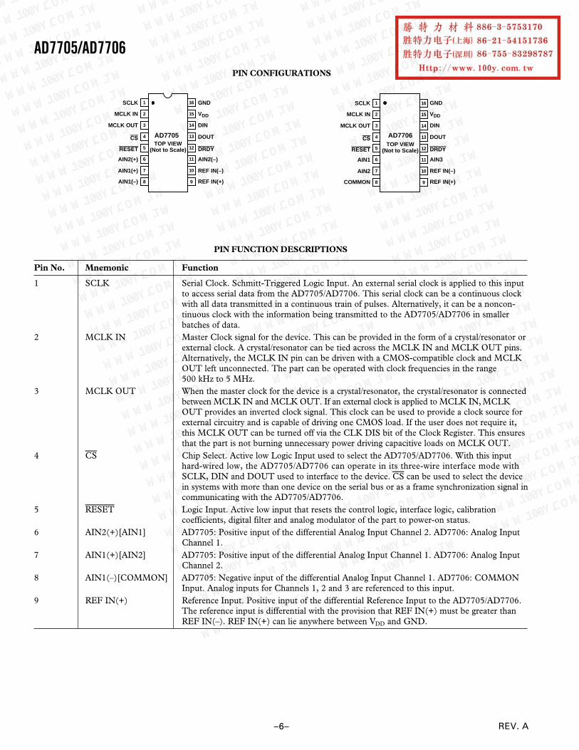
PIN FUNCTION DESCRIPTIONS
Pin No. Mnemonic Function
1 SCLK Serial Clock. Schmitt-Triggered Logic Input. An external serial clock is applied to this inputto access serial data from the AD7705/AD7706. This serial clock can be a continuous clockwith all data transmitted in a continuous train of pulses. Alternatively, it can be a noncon-tinuous clock with the information being transmitted to the AD7705/AD7706 in smallerbatches of data.
2 MCLK IN Master Clock signal for the device. This can be provided in the form of a crystal/resonator orexternal clock. A crystal/resonator can be tied across the MCLK IN and MCLK OUT pins.Alternatively, the MCLK IN pin can be driven with a CMOS-compatible clock and MCLKOUT left unconnected. The part can be operated with clock frequencies in the range500 kHz to 5 MHz.
3 MCLK OUT When the master clock for the device is a crystal/resonator, the crystal/resonator is connectedbetween MCLK IN and MCLK OUT. If an external clock is applied to MCLK IN, MCLKOUT provides an inverted clock signal. This clock can be used to provide a clock source forexternal circuitry and is capable of driving one CMOS load. If the user does not require it,this MCLK OUT can be turned off via the CLK DIS bit of the Clock Register. This ensuresthat the part is not burning unnecessary power driving capacitive loads on MCLK OUT.
4 CS Chip Select. Active low Logic Input used to select the AD7705/AD7706. With this inputhard-wired low, the AD7705/AD7706 can operate in its three-wire interface mode withSCLK, DIN and DOUT used to interface to the device. CS can be used to select the devicein systems with more than one device on the serial bus or as a frame synchronization signal incommunicating with the AD7705/AD7706.
5 RESET Logic Input. Active low input that resets the control logic, interface logic, calibrationcoefficients, digital filter and analog modulator of the part to power-on status.
6 AIN2(+)[AIN1] AD7705: Positive input of the differential Analog Input Channel 2. AD7706: Analog InputChannel 1.
7 AIN1(+)[AIN2] AD7705: Positive input of the differential Analog Input Channel 1. AD7706: Analog InputChannel 2.
8 AIN1(–)[COMMON] AD7705: Negative input of the differential Analog Input Channel 1. AD7706: COMMONInput. Analog inputs for Channels 1, 2 and 3 are referenced to this input.
9 REF IN(+) Reference Input. Positive input of the differential Reference Input to the AD7705/AD7706.The reference input is differential with the provision that REF IN(+) must be greater thanREF IN(–). REF IN(+) can lie anywhere between VDD and GND.
PIN CONFIGURATIONS
TOP VIEW(Not to Scale)
16
15
14
13
12
11
10
9
1
2
3
4
5
6
7
8
SCLK
MCLK IN
MCLK OUT
CS
RESET
AIN2(+)
AIN1(+)
AIN1(–)
GND
VDD
DIN
DOUT
DRDY
AIN2(–)
REF IN(–)
REF IN(+)
AD7705TOP VIEW
(Not to Scale)
16
15
14
13
12
11
10
9
1
2
3
4
5
6
7
8
SCLK
MCLK IN
MCLK OUT
CS
RESET
AIN1
AIN2
COMMON
GND
VDD
DIN
DOUT
DRDY
AIN3
REF IN(–)
REF IN(+)
AD7706
AD7705/AD7706
–7–REV. A
Pin No. Mnemonic Function
10 REF IN(–) Reference Input. Negative input of the differential reference input to the AD7705/AD7706.The REF IN(–) can lie anywhere between VDD and GND provided REF IN(+) is greaterthan REF IN(–).
11 AIN2(–)[AIN3] AD7705: Negative input of the differential analog Input Channel 2. AD7706: Analog InputChannel 3.
12 DRDY Logic Output. A logic low on this output indicates that a new output word is available fromthe AD7705/AD7706 data register. The DRDY pin will return high upon completion of aread operation of a full output word. If no data read has taken place between output updates,the DRDY line will return high for 500 × tCLK IN cycles prior to the next output update.While DRDY is high, a read operation should neither be attempted nor in progress to avoidreading from the data register as it is being updated. The DRDY line will return low againwhen the update has taken place. DRDY is also used to indicate when the AD7705/AD7706has completed its on-chip calibration sequence.
13 DOUT Serial Data Output with serial data being read from the output shift register on the part. Thisoutput shift register can contain information from the setup register, communications regis-ter, clock register or data register, depending on the register selection bits of the Communica-tions Register.
14 DIN Serial Data Input with serial data being written to the input shift register on the part. Datafrom this input shift register is transferred to the setup register, clock register or communica-tions register, depending, on the register selection bits of the Communications Register.
15 VDD Supply Voltage, +2.7 V to +5.25 V operation.16 GND Ground reference point for the AD7705/AD7706’s internal circuitry.
OUTPUT NOISE (5 V OPERATION)Table I shows the AD7705/AD7706 output rms noise for the selectable notch and –3 dB frequencies for the part, as selected by FS0and FS1 of the Clock Register. The numbers given are for the bipolar input ranges with a VREF of +2.5 V and VDD = 5 V. Thesenumbers are typical and are generated at an analog input voltage of 0 V with the part used in either buffered or unbuffered mode. Table IImeanwhile shows the output peak-to-peak noise for the selectable notch and –3 dB frequencies for the part. It is important to note thatthese numbers represent the resolution for which there will be no code flicker. They are not calculated based on rms noise but on peak-to-peaknoise. The numbers given are for bipolar input ranges with a VREF of +2.5 V and for either buffered or unbuffered mode. These num-bers are typical and are rounded to the nearest LSB. The numbers apply for the CLK DIV bit of the Clock Register set to 0.
Table I. Output RMS Noise vs. Gain and Output Update Rate @ 5 V
Filter First Typical Output RMS Noise in mVNotch and O/P –3 dB Gain of Gain of Gain of Gain of Gain of Gain of Gain of Gain ofData Rate Frequency 1 2 4 8 16 32 64 128
MCLK IN = 2.4576 MHz50 Hz 13.1 Hz 4.1 2.1 1.2 0.75 0.7 0.66 0.63 0.660 Hz 15.72 Hz 5.1 2.5 1.4 0.8 0.75 0.7 0.67 0.62250 Hz 65.5 Hz 110 49 31 17 8 3.6 2.3 1.7500 Hz 131 Hz 550 285 145 70 41 22 9.1 4.7MCLK IN = 1 MHz20 Hz 5.24 Hz 4.1 2.1 1.2 0.75 0.7 0.66 0.63 0.625 Hz 6.55 Hz 5.1 2.5 1.4 0.8 0.75 0.7 0.67 0.62100 Hz 26.2 Hz 110 49 31 17 8 3.6 2.3 1.7200 Hz 52.4 Hz 550 285 145 70 41 22 9.1 4.7
AD7705/AD7706
–8– REV. A
Table II. Peak-to-Peak Resolution vs. Gain and Output Update Rate @ 5 V
Filter First Typical Peak-to-Peak Resolution BitsNotch and O/P –3 dB Gain of Gain of Gain of Gain of Gain of Gain of Gain of Gain ofData Rate Frequency 1 2 4 8 16 32 64 128
MCLK IN = 2.4576 MHz50 Hz 13.1 Hz 16 16 16 16 16 16 15 1460 Hz 15.72 Hz 16 16 16 16 15 14 14 13250 Hz 65.5 Hz 13 13 13 13 13 13 12 12500 Hz 131 Hz 10 10 10 10 10 10 10 10MCLK IN = 1 MHz20 Hz 5.24 Hz 16 16 16 16 16 16 15 1425 Hz 6.55 Hz 16 16 16 16 15 14 14 13100 Hz 26.2 Hz 13 13 13 13 13 13 12 12200 Hz 52.4 Hz 10 10 10 10 10 10 10 10
OUTPUT NOISE (3 V OPERATION)Table III shows the AD7705/AD7706 output rms noise for the selectable notch and –3 dB frequencies for the part, as selected byFS0 and FS1 of the Clock Register. The numbers given are for the bipolar input ranges with a VREF of +1.225 V and a VDD = 3 V.These numbers are typical and are generated at an analog input voltage of 0 V with the part used in either buffered or unbufferedmode. Table II meanwhile shows the output peak-to-peak noise for the selectable notch and –3 dB frequencies for the part. It is im-portant to note that these numbers represent the resolution for which there will be no code flicker. They are not calculated based on rms noise buton peak-to-peak noise. The numbers given are for bipolar input ranges with a VREF of +1.225 V and for either buffered or unbufferedmode. These numbers are typical and are rounded to the nearest LSB. The numbers apply for the CLK DIV bit of the Clock Regis-ter set to 0.
Table III. Output RMS Noise vs. Gain and Output Update Rate @ 3 V
Filter First Typical Output RMS Noise in mVNotch and O/P –3 dB Gain of Gain of Gain of Gain of Gain of Gain of Gain of Gain ofData Rate Frequency 1 2 4 8 16 32 64 128
MCLK IN = 2.4576 MHz50 Hz 13.1 Hz 3.8 2.4 1.5 1.3 1.1 1.0 0.9 0.960 Hz 15.72 Hz 5.1 2.9 1.7 1.5 1.2 1.0 0.9 0.9250 Hz 65.5 Hz 50 25 14 9.9 5.1 2.6 2.3 2.0500 Hz 131 Hz 270 135 65 41 22 9.7 5.1 3.3MCLK IN = 1 MHz20 Hz 5.24 Hz 3.8 2.4 1.5 1.3 1.1 1.0 0.9 0.925 Hz 6.55 Hz 5.1 2.9 1.7 1.5 1.2 1.0 0.9 0.9100 Hz 26.2 Hz 50 25 14 9.9 5.1 2.6 2.3 2.0200 Hz 52.4 Hz 270 135 65 41 22 9.7 5.1 3.3
Table IV. Peak-to-Peak Resolution vs. Gain and Output Update Rate @ 3 V
Filter First Typical Peak-to-Peak Resolution in BitsNotch and O/P –3 dB Gain of Gain of Gain of Gain of Gain of Gain of Gain of Gain ofData Rate Frequency 1 2 4 8 16 32 64 128
MCLK IN = 2.4576 MHz50 Hz 13.1 Hz 16 16 15 15 14 13 13 1260 Hz 15.72 Hz 16 16 15 14 14 13 13 12250 Hz 65.5 Hz 13 13 13 13 12 12 11 11500 Hz 131 Hz 10 10 10 10 10 10 10 10MCLK IN = 1 MHz20 Hz 5.24 Hz 16 16 15 15 14 13 13 1225 Hz 6.55 Hz 16 16 15 14 14 13 13 12100 Hz 26.2 Hz 13 13 13 13 12 12 11 11200 Hz 52.4 Hz 10 10 10 10 10 10 10 10
AD7705/AD7706
–9–REV. A
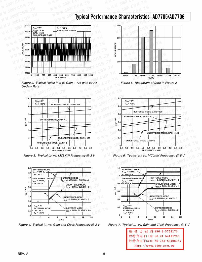
Typical Performance Characteristics–
READING NO.
327630 100
CO
DE
RE
AD
32764
32765
32766
32767
32768
32769
32770
32771
200 300 400 500 600 700 800 900 1000
VDD = 5VVREF = 2.5VGAIN = 12850Hz UPDATE RATE
TA = +258CRMS NOISE = 600nV
Figure 2. Typical Noise Plot @ Gain = 128 with 50 HzUpdate Rate
FREQUENCY – MHz0.4
I DD
– m
A
VDD = 3VTA = +258C
1.2
1.0
0.8
0.6
0.4
0.2
00.6 0.8 1.0 1.2 1.4 1.6 1.8 2.0 2.2 2.4 2.6
BUFFERED MODE, GAIN = 128
UNBUFFERED MODE, GAIN = 1
UNBUFFERED MODE, GAIN = 128
BUFFERED MODE, GAIN = 1
Figure 3. Typical IDD vs. MCLKIN Frequency @ 3 V
GAIN1
I DD
– m
A
VDD = 3VEXTERNAL MCLKCLKDIS = 1TA = +258C
1.0
0.8
0.6
0.4
0.2
0
0.1
0.3
0.5
0.7
0.9
2 4 8 16 32 64 128
BUFFERED MODEfCLK = 5MHz,CLKDIV = 1
BUFFERED MODEfCLK = 1MHz, CLKDIV = 0
BUFFERED MODEfCLK = 2.4576MHz, CLKDIV = 0
UNBUFFERED MODEfCLK = 2.84MHz, CLKDIV = 0
UNBUFFERED MODEfCLK = 1MHz,CLKDIV = 0
UNBUFFERED MODEfCLK = 5MHz, CLKDIV = 1
Figure 4. Typical IDD vs. Gain and Clock Frequency @ 3 V
CODE32764
OC
CU
RR
EN
CE
400
032765 32766 32767 32768 32769 32770
300
200
100
Figure 5. Histogram of Data in Figure 2
FREQUENCY – MHz0.4
I DD
– m
A
VDD = 5VTA = +258C
1.2
1.0
0.8
0.6
0.4
0.2
00.6 0.8 1.0 1.2 1.4 1.6 1.8 2.0 2.2 2.4 2.6
BUFFERED MODE, GAIN = 128
UNBUFFERED MODE, GAIN = 1
UNBUFFERED MODE, GAIN = 128
BUFFERED MODE, GAIN = 1
Figure 6. Typical IDD vs. MCLKIN Frequency @ 5 V
GAIN1
I DD
– m
A
VDD = 5VEXTERNAL MCLKCLKDIS = 1TA = +258C
1.2
0.8
0.6
0.4
0.2
0
1.0
2 4 8 16 32 64 128
BUFFERED MODEfCLK = 5MHz,CLKDIV = 1
BUFFERED MODEfCLK = 1MHz, CLKDIV = 0
BUFFERED MODEfCLK = 2.4576MHz, CLKDIV = 0
UNBUFFERED MODEfCLK = 2.4576MHz, CLKDIV = 0
UNBUFFERED MODEfCLK = 1MHz,CLKDIV = 0 UNBUFFERED MODE
fCLK = 5MHz, CLKDIV = 1
Figure 7. Typical IDD vs. Gain and Clock Frequency @ 5 V
AD7705/AD7706
–10– REV. A
ON-CHIP REGISTERSThe AD7705/AD7706 contains eight on-chip registers which can be accessed via the serial port of the part. The first of these is aCommunications Register that controls the channel selection, decides whether the next operation is a read or write operation andalso decides which register the next read or write operation accesses. All communications to the part must start with a write opera-tion to the Communications Register. After power-on or RESET, the device expects a write to its Communications Register. Thedata written to this register determines whether the next operation to the part is a read or a write operation and also determines towhich register this read or write operation occurs. Therefore, write access to any of the other registers on the part starts with a writeoperation to the Communications Register followed by a write to the selected register. A read operation from any other register onthe part (including the Communications Register itself and the output data register) starts with a write operation to the Communica-tions Register followed by a read operation from the selected register. The Communications Register also controls the standby modeand channel selection and the DRDY status is also available by reading from the Communications Register. The second register is aSetup Register that determines calibration mode, gain setting, bipolar/unipolar operation and buffered mode. The third register islabelled the Clock Register and contains the filter selection bits and clock control bits. The fourth register is the Data Register fromwhich the output data from the part is accessed. The final registers are the calibration registers which store channel calibration data.The registers are discussed in more detail in the following sections.
Communications Register (RS2, RS1, RS0 = 0, 0, 0)The Communications Register is an 8-bit register from which data can either be read or to which data can be written. All communi-cations to the part must start with a write operation to the Communications Register. The data written to the Communications Reg-ister determines whether the next operation is a read or write operation and to which register this operation takes place. Once thesubsequent read or write operation to the selected register is complete, the interface returns to where it expects a write operation tothe Communications Register. This is the default state of the interface, and on power-up or after a RESET, the AD7705/AD7706 isin this default state waiting for a write operation to the Communications Register. In situations where the interface sequence is lost,if a write operation of sufficient duration (containing at least 32 serial clock cycles) takes place with DIN high, the AD7705 returnsto this default state. Table V outlines the bit designations for the Communications Register.
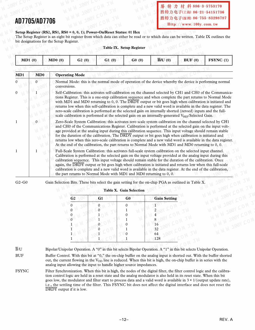
Table V. Communications Register
0/DRDY (0) RS2 (0) RS1 (0) RS0 (0) R/W (0) STBY (0) CH1 (0) CH0 (0)
0/DRDY For a write operation, a “0” must be written to this bit so that the write operation to the Communications Registeractually takes place. If a “1” is written to this bit, the part will not clock on to subsequent bits in the register. Itwill stay at this bit location until a “0” is written to this bit. Once a “0” is written to this bit, the next seven bitswill be loaded to the Communications Register. For a read operation, this bit provides the status of the DRDY flagfrom the part. The status of this bit is the same as the DRDY output pin.
RS2–RS0 Register Selection Bits. These three bits select to which one of eight on-chip registers the next read or write opera-tion takes place, as shown in Table VI, along with the register size. When the read or write operation to the se-lected register is complete, the part returns to where it is waiting for a write operation to the CommunicationsRegister. It does not remain in a state where it will continue to access the register.
TEMPERATURE – 8C–40
ST
AN
DB
Y C
UR
RE
NT
– m
A
0
4
8
16
20
12
–30 –20 –10 0 10 20 30 40 50 60 70 80
VDD = 5V
VDD = 3V
MCLK IN = 0V OR VDD
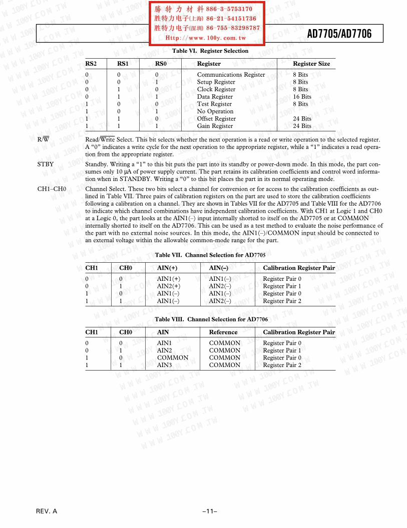
Figure 9. Standby Current vs. Temperature
CH1 5.00V CH2 2.00V
2
2
1
TEK STOP: SINGLE SEQ 50.0kS/s
VDD
OSCILLATOR = 4.9152 MHz
OSCILLATOR = 2.4576 MHz
5ms/DIV
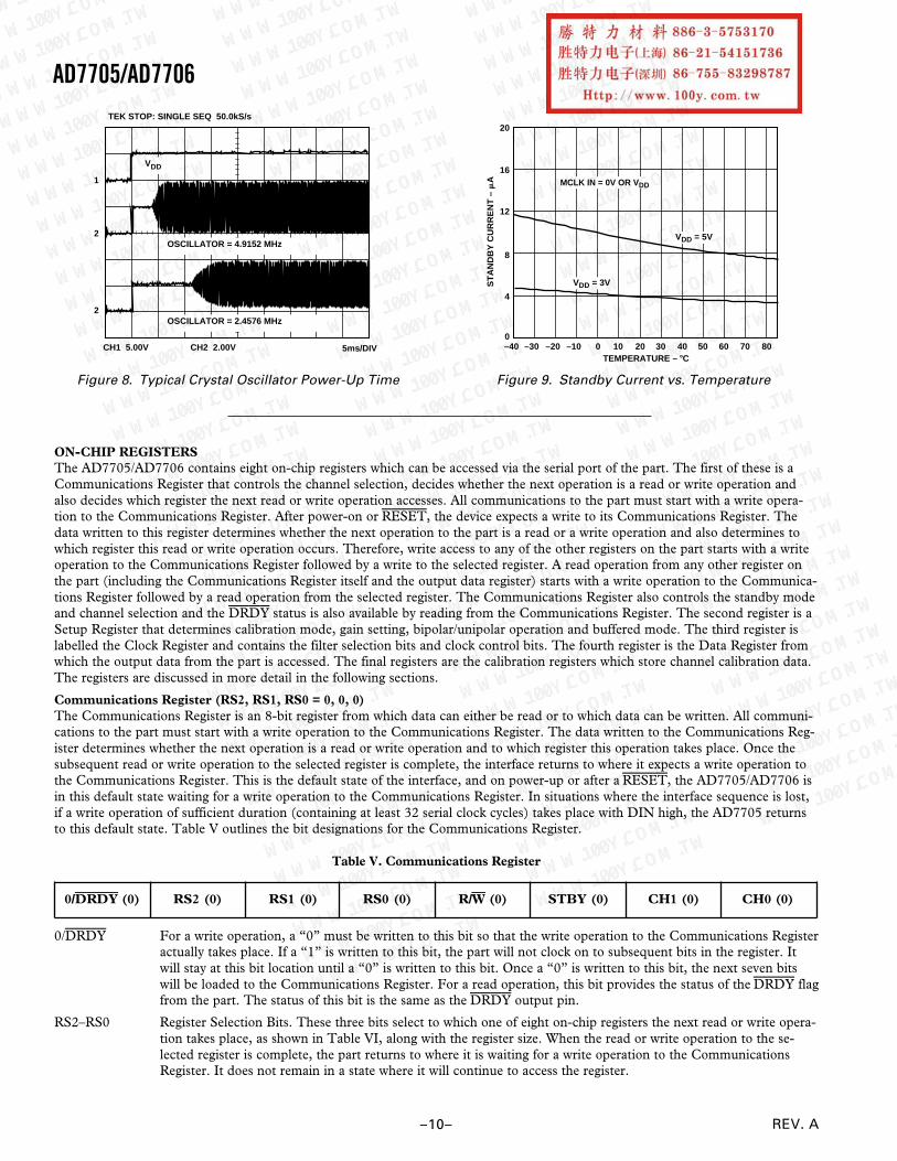
Figure 8. Typical Crystal Oscillator Power-Up Time
AD7705/AD7706
–11–REV. A
Table VI. Register Selection
RS2 RS1 RS0 Register Register Size
0 0 0 Communications Register 8 Bits0 0 1 Setup Register 8 Bits0 1 0 Clock Register 8 Bits0 1 1 Data Register 16 Bits1 0 0 Test Register 8 Bits1 0 1 No Operation1 1 0 Offset Register 24 Bits1 1 1 Gain Register 24 Bits
R/W Read/Write Select. This bit selects whether the next operation is a read or write operation to the selected register.A “0” indicates a write cycle for the next operation to the appropriate register, while a “1” indicates a read opera-tion from the appropriate register.
STBY Standby. Writing a “1” to this bit puts the part into its standby or power-down mode. In this mode, the part con-sumes only 10 µA of power supply current. The part retains its calibration coefficients and control word informa-tion when in STANDBY. Writing a “0” to this bit places the part in its normal operating mode.
CH1–CH0 Channel Select. These two bits select a channel for conversion or for access to the calibration coefficients as out-lined in Table VII. Three pairs of calibration registers on the part are used to store the calibration coefficientsfollowing a calibration on a channel. They are shown in Tables VII for the AD7705 and Table VIII for the AD7706to indicate which channel combinations have independent calibration coefficients. With CH1 at Logic 1 and CH0at a Logic 0, the part looks at the AIN1(–) input internally shorted to itself on the AD7705 or at COMMONinternally shorted to itself on the AD7706. This can be used as a test method to evaluate the noise performance ofthe part with no external noise sources. In this mode, the AIN1(–)/COMMON input should be connected toan external voltage within the allowable common-mode range for the part.
Table VII. Channel Selection for AD7705
CH1 CH0 AIN(+) AIN(–) Calibration Register Pair
0 0 AIN1(+) AIN1(–) Register Pair 00 1 AIN2(+) AIN2(–) Register Pair 11 0 AIN1(–) AIN1(–) Register Pair 01 1 AIN1(–) AIN2(–) Register Pair 2
Table VIII. Channel Selection for AD7706
CH1 CH0 AIN Reference Calibration Register Pair
0 0 AIN1 COMMON Register Pair 00 1 AIN2 COMMON Register Pair 11 0 COMMON COMMON Register Pair 01 1 AIN3 COMMON Register Pair 2
AD7705/AD7706
–12– REV. A
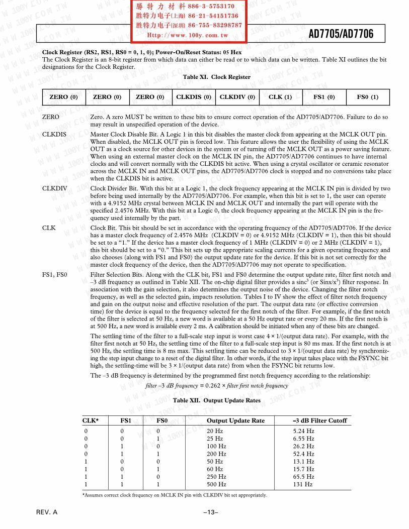
Setup Register (RS2, RS1, RS0 = 0, 0, 1); Power-On/Reset Status: 01 HexThe Setup Register is an eight bit register from which data can either be read or to which data can be written. Table IX outlines thebit designations for the Setup Register.
Table IX. Setup Register
MD1 (0) MD0 (0) G2 (0) G1 (0) G0 (0) B/U (0) BUF (0) FSYNC (1)
MD1 MD0 Operating Mode
0 0 Normal Mode: this is the normal mode of operation of the device whereby the device is performing normalconversions.
0 1 Self-Calibration: this activates self-calibration on the channel selected by CH1 and CH0 of the Communica-tions Register. This is a one-step calibration sequence and when complete the part returns to Normal Modewith MD1 and MD0 returning to 0, 0. The DRDY output or bit goes high when calibration is initiated andreturns low when this self-calibration is complete and a new valid word is available in the data register. Thezero-scale calibration is performed at the selected gain on internally shorted (zeroed) inputs and the full-scale calibration is performed at the selected gain on an internally-generated VREF/Selected Gain.
1 0 Zero-Scale System Calibration: this activates zero scale system calibration on the channel selected by CH1and CH0 of the Communications Register. Calibration is performed at the selected gain on the input volt-age provided at the analog input during this calibration sequence. This input voltage should remain stablefor the duration of the calibration. The DRDY output or bit goes high when calibration is initiated andreturns low when this zero-scale calibration is complete and a new valid word is available in the data register.At the end of the calibration, the part returns to Normal Mode with MD1 and MD0 returning to 0, 0.
1 1 Full-Scale System Calibration: this activates full-scale system calibration on the selected input channel.Calibration is performed at the selected gain on the input voltage provided at the analog input during thiscalibration sequence. This input voltage should remain stable for the duration of the calibration. Onceagain, the DRDY output or bit goes high when calibration is initiated and returns low when this full-scalecalibration is complete and a new valid word is available in the data register. At the end of the calibration,the part returns to Normal Mode with MD1 and MD0 returning to 0, 0.
G2–G0 Gain Selection Bits. These bits select the gain setting for the on-chip PGA as outlined in Table X.
Table X. Gain Selection
G2 G1 G0 Gain Setting
0 0 0 10 0 1 20 1 0 40 1 1 81 0 0 161 0 1 321 1 0 641 1 1 128
B/U Bipolar/Unipolar Operation. A “0” in this bit selects Bipolar Operation. A “1” in this bit selects Unipolar Operation.
BUF Buffer Control. With this bit at “0,” the on-chip buffer on the analog input is shorted out. With the buffer shortedout, the current flowing in the VDD line is reduced. When this bit is high, the on-chip buffer is in series with theanalog input allowing the input to handle higher source impedances.
FSYNC Filter Synchronization. When this bit is high, the nodes of the digital filter, the filter control logic and the calibra-tion control logic are held in a reset state and the analog modulator is also held in its reset state. When this bitgoes low, the modulator and filter start to process data and a valid word is available in 3 × 1/(output update rate),i.e., the settling time of the filter. This FSYNC bit does not affect the digital interface and does not reset theDRDY output if it is low.
AD7705/AD7706
–13–REV. A
Clock Register (RS2, RS1, RS0 = 0, 1, 0); Power-On/Reset Status: 05 HexThe Clock Register is an 8-bit register from which data can either be read or to which data can be written. Table XI outlines the bitdesignations for the Clock Register.
Table XI. Clock Register
ZERO (0) ZERO (0) ZERO (0) CLKDIS (0) CLKDIV (0) CLK (1) FS1 (0) FS0 (1)
ZERO Zero. A zero MUST be written to these bits to ensure correct operation of the AD7705/AD7706. Failure to do somay result in unspecified operation of the device.
CLKDIS Master Clock Disable Bit. A Logic 1 in this bit disables the master clock from appearing at the MCLK OUT pin.When disabled, the MCLK OUT pin is forced low. This feature allows the user the flexibility of using the MCLKOUT as a clock source for other devices in the system or of turning off the MCLK OUT as a power saving feature.When using an external master clock on the MCLK IN pin, the AD7705/AD7706 continues to have internalclocks and will convert normally with the CLKDIS bit active. When using a crystal oscillator or ceramic resonatoracross the MCLK IN and MCLK OUT pins, the AD7705/AD7706 clock is stopped and no conversions take placewhen the CLKDIS bit is active.
CLKDIV Clock Divider Bit. With this bit at a Logic 1, the clock frequency appearing at the MCLK IN pin is divided by twobefore being used internally by the AD7705/AD7706. For example, when this bit is set to 1, the user can operatewith a 4.9152 MHz crystal between MCLK IN and MCLK OUT and internally the part will operate with thespecified 2.4576 MHz. With this bit at a Logic 0, the clock frequency appearing at the MCLK IN pin is the fre-quency used internally by the part.
CLK Clock Bit. This bit should be set in accordance with the operating frequency of the AD7705/AD7706. If the devicehas a master clock frequency of 2.4576 MHz (CLKDIV = 0) or 4.9152 MHz (CLKDIV = 1), then this bit shouldbe set to a “1.” If the device has a master clock frequency of 1 MHz (CLKDIV = 0) or 2 MHz (CLKDIV = 1),this bit should be set to a “0.” This bit sets up the appropriate scaling currents for a given operating frequency andalso chooses (along with FS1 and FS0) the output update rate for the device. If this bit is not set correctly for themaster clock frequency of the device, then the AD7705/AD7706 may not operate to specification.
FS1, FS0 Filter Selection Bits. Along with the CLK bit, FS1 and FS0 determine the output update rate, filter first notch and–3 dB frequency as outlined in Table XII. The on-chip digital filter provides a sinc3 (or Sinx/x3) filter response. Inassociation with the gain selection, it also determines the output noise of the device. Changing the filter notchfrequency, as well as the selected gain, impacts resolution. Tables I to IV show the effect of filter notch frequencyand gain on the output noise and effective resolution of the part. The output data rate (or effective conversiontime) for the device is equal to the frequency selected for the first notch of the filter. For example, if the first notchof the filter is selected at 50 Hz, a new word is available at a 50 Hz output rate or every 20 ms. If the first notch isat 500 Hz, a new word is available every 2 ms. A calibration should be initiated when any of these bits are changed.
The settling time of the filter to a full-scale step input is worst case 4 × 1/(output data rate). For example, with thefilter first notch at 50 Hz, the settling time of the filter to a full-scale step input is 80 ms max. If the first notch is at500 Hz, the settling time is 8 ms max. This settling time can be reduced to 3 × 1/(output data rate) by synchroniz-ing the step input change to a reset of the digital filter. In other words, if the step input takes place with the FSYNC bithigh, the settling-time will be 3 × 1/(output data rate) from when the FSYNC bit returns low.
The –3 dB frequency is determined by the programmed first notch frequency according to the relationship:
filter –3 dB frequency = 0.262 × filter first notch frequency
Table XII. Output Update Rates
CLK* FS1 FS0 Output Update Rate –3 dB Filter Cutoff
0 0 0 20 Hz 5.24 Hz0 0 1 25 Hz 6.55 Hz0 1 0 100 Hz 26.2 Hz0 1 1 200 Hz 52.4 Hz1 0 0 50 Hz 13.1 Hz1 0 1 60 Hz 15.7 Hz1 1 0 250 Hz 65.5 Hz1 1 1 500 Hz 131 Hz
*Assumes correct clock frequency on MCLK IN pin with CLKDIV bit set appropriately.
AD7705/AD7706
–14– REV. A
Data Register (RS2, RS1, RS0 = 0, 1, 1)The Data Register on the part is a 16-bit read-only register that contains the most up-to-date conversion result from the AD7705/AD7706. If the Communications Register sets up the part for a write operation to this register, a write operation must actually takeplace to return the part to where it is expecting a write operation to the Communications Register. However, the 16 bits of datawritten to the part will be ignored by the AD7705/AD7706.
Test Register (RS2, RS1, RS0 = 1, 0, 0); Power-On/Reset Status: 00 HexThe part contains a Test Register that is used when testing the device. The user is advised not to change the status of any of the bitsin this register from the default (Power-on or RESET) status of all 0s as the part will be placed in one of its test modes and will notoperate correctly.
Zero-Scale Calibration Register (RS2, RS1, RS0 = 1, 1, 0); Power-On/Reset Status: 1F4000 HexThe AD7705/AD7706 contains independent sets of zero-scale registers, one for each of the input channels. Each of these registers isa 24-bit read/write register; 24 bits of data must be written otherwise no data will be transferred to the register. This register is usedin conjunction with its associated full-scale register to form a register pair. These register pairs are associated with input channelpairs as outlined in Table VII. While the part is set up to allow access to these registers over the digital interface, the part itself nolonger has access to the register coefficients to correctly scale the output data. As a result, there is a possibility that after accessing thecalibration registers (either read or write operation) the first output data read from the part may contain incorrect data. In addition, awrite to the calibration register should not be attempted while a calibration is in progress. These eventualities can be avoided bytaking the FSYNC bit in the mode register high before the calibration register operation and taking it low after the operation iscomplete.
Full-Scale Calibration Register (RS2, RS1, RS0 = 1, 1, 1); Power-On/Reset Status: 5761AB HexThe AD7705/AD7706 contains independent sets of full-scale registers, one for each of the input channels. Each of these registers is a24-bit read/write register; 24 bits of data must be written otherwise no data will be transferred to the register. This register is used inconjunction with its associated zero-scale register to form a register pair. These register pairs are associated with input channel pairsas outlined in Table VII. While the part is set up to allow access to these registers over the digital interface, the part itself no longerhas access to the register coefficients to correctly scale the output data. As a result, there is a possibility that after accessing the cali-bration registers (either read or write operation) the first output data read from the part may contain incorrect data. In addition, awrite to the calibration register should not be attempted while a calibration is in progress. These eventualities can be avoided bytaking FSYNC bit in the mode register high before the calibration register operation and taking it low after the operation is complete.
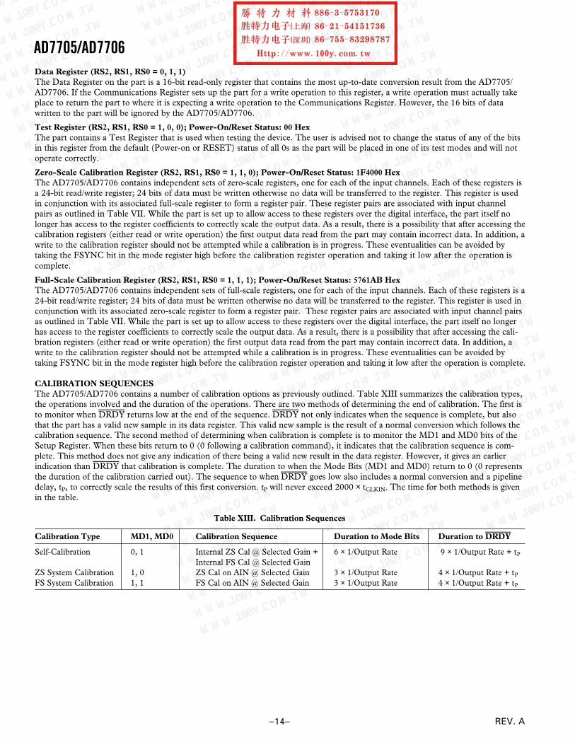
CALIBRATION SEQUENCESThe AD7705/AD7706 contains a number of calibration options as previously outlined. Table XIII summarizes the calibration types,the operations involved and the duration of the operations. There are two methods of determining the end of calibration. The first isto monitor when DRDY returns low at the end of the sequence. DRDY not only indicates when the sequence is complete, but alsothat the part has a valid new sample in its data register. This valid new sample is the result of a normal conversion which follows thecalibration sequence. The second method of determining when calibration is complete is to monitor the MD1 and MD0 bits of theSetup Register. When these bits return to 0 (0 following a calibration command), it indicates that the calibration sequence is com-plete. This method does not give any indication of there being a valid new result in the data register. However, it gives an earlierindication than DRDY that calibration is complete. The duration to when the Mode Bits (MD1 and MD0) return to 0 (0 representsthe duration of the calibration carried out). The sequence to when DRDY goes low also includes a normal conversion and a pipelinedelay, tP, to correctly scale the results of this first conversion. tP will never exceed 2000 × tCLKIN. The time for both methods is givenin the table.
Table XIII. Calibration Sequences
Calibration Type MD1, MD0 Calibration Sequence Duration to Mode Bits Duration to DRDY
Self-Calibration 0, 1 Internal ZS Cal @ Selected Gain + 6 × 1/Output Rate 9 × 1/Output Rate + tP
Internal FS Cal @ Selected GainZS System Calibration 1, 0 ZS Cal on AIN @ Selected Gain 3 × 1/Output Rate 4 × 1/Output Rate + tP
FS System Calibration 1, 1 FS Cal on AIN @ Selected Gain 3 × 1/Output Rate 4 × 1/Output Rate + tP
AD7705/AD7706
–15–REV. A
CIRCUIT DESCRIPTIONThe AD7705/AD7706 is a sigma-delta A/D converter with on-chip digital filtering, intended for the measurement of widedynamic range, low frequency signals such as those in industrialcontrol or process control applications. It contains a sigma-delta(or charge-balancing) ADC, a calibration microcontroller withon-chip static RAM, a clock oscillator, a digital filter and a bi-directional serial communications port. The part consumes only320 µA of power supply current, making it ideal for battery-powered or loop-powered instruments. These parts operate witha supply voltage of 2.7 V to 3.3 V or 4.75 V to 5.25 V.
The AD7705 contains two programmable-gain fully differentialanalog input channels, while the AD7706 contains three pseudodifferential analog input channels. The selectable gains on theseinputs are 1, 2, 4, 8, 16, 32, 64 and 128 allowing the part toaccept unipolar signals of between 0 mV to +20 mV and 0 V to+2.5 V, or bipolar signals in the range from ±20 mV to ±2.5 Vwhen the reference input voltage equals +2.5 V. With a refer-ence voltage of +1.225 V, the input ranges are from 0 mV to+10 mV to 0 V to +1.225 V in unipolar mode, and from ±10 mVto ±1.225 V in bipolar mode. Note that the bipolar ranges arewith respect to AIN(–) on the AD7705, and with respect toCOMMON on the AD7706, and not with respect to GND.
The input signal to the analog input is continuously sampledat a rate determined by the frequency of the master clock,MCLK IN, and the selected gain. A charge-balancing A/Dconverter (Sigma-Delta Modulator) converts the sampled signalinto a digital pulse train whose duty cycle contains the digitalinformation. The programmable gain function on the analog
input is also incorporated in this sigma-delta modulator with theinput sampling frequency being modified to give the highergains. A sinc3 digital low-pass filter processes the output of thesigma-delta modulator and updates the output register at a ratedetermined by the first notch frequency of this filter. The out-put data can be read from the serial port randomly or periodi-cally at any rate up to the output register update rate. The firstnotch of this digital filter (and hence its –3 dB frequency) canbe programmed via the Setup Register bits FS0 and FS1. Witha master clock frequency of 2.4576 MHz, the programmablerange for this first notch frequency is from 50 Hz to 500 Hz,giving a programmable range for the –3 dB frequency of13.1 Hz to 131 Hz. With a master clock frequency of 1 MHz,the programmable range for this first notch frequency is from20 Hz to 200 Hz, giving a programmable range for the –3 dBfrequency of 5.24 Hz to 52.4 Hz.
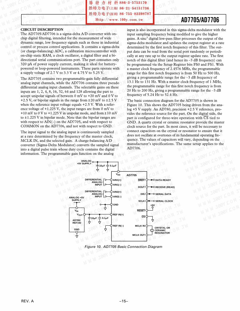
The basic connection diagram for the AD7705 is shown inFigure 10. This shows the AD7705 being driven from the ana-log +5 V supply. An AD780, precision +2.5 V reference, pro-vides the reference source for the part. On the digital side, thepart is configured for three-wire operation with CS tied toGND. A quartz crystal or ceramic resonator provide the masterclock source for the part. In most cases, it will be necessary toconnect capacitors on the crystal or resonator to ensure that itdoes not oscillate at overtones of its fundamental operating fre-quency. The values of capacitors will vary, depending on themanufacturer’s specifications. The same setup applies to theAD7706.
VDD
ANALOG+5V SUPPLY
10mF
AIN1(+)
AIN1(–)
AIN2(+)
AIN2(–)
DIFFERENTIALANALOG
INPUT
DIFFERENTIALANALOG
INPUT
GND
REF IN(+)
REF IN(–)
10mF
VIN
ANALOG +5VSUPPLY
AD780/REF192
VOUT
GND
AD7705
DRDY DATA READY
DOUT RECEIVE (READ)
DIN SERIAL DATA
SCLK SERIAL CLOCK
RESET
+5V
CS
MCLK IN
MCLK OUT
CRYSTAL ORCERAMICRESONATOR
0.1mF
0.1mF
Figure 10. AD7705 Basic Connection Diagram

AD7705/AD7706
–16– REV. A
ANALOG INPUTAnalog Input RangesThe AD7705 contains two differential analog input pairsAIN1(+), AIN1(–) and AIN2(+), AIN2(–). These input pairsprovide programmable-gain, differential input channels thatcan handle either unipolar or bipolar input signals. It should benoted that the bipolar input signals are referenced to the re-spective AIN(–) input of each input pair. The AD7706 containsthree pseudo differential analog input pairs AIN1, AIN2 andAIN3, which are referenced to the COMMON input on the part.
In unbuffered mode, the common-mode range of the input isfrom GND to VDD, provided that the absolute value of theanalog input voltage lies between GND – 30 mV and VDD
+ 30 mV. This means that in unbuffered mode the part canhandle both unipolar and bipolar input ranges for all gains.Absolute voltages of GND – 200 mV can be accommodated onthe analog inputs at 25°C without degradation in performance,but leakage current increases appreciably with increasing tem-perature. In buffered mode, the analog inputs can handlemuch larger source impedances, but the absolute input voltagerange is restricted to between GND + 50 mV to VDD – 1.5 Vwhich also places restrictions on the common-mode range. Thismeans that in buffered mode there are some restrictions on theallowable gains for bipolar input ranges. Care must be taken insetting up the common-mode voltage and input voltage rangeso that the above limits are not exceeded, otherwise there willbe a degradation in linearity performance.
In unbuffered mode, the analog inputs look directly into the7 pF input sampling capacitor, CSAMP. The dc input leakagecurrent in this unbuffered mode is 1 nA maximum. As a result,the analog inputs see a dynamic load that is switched at theinput sample rate (see Figure 11). This sample rate depends onmaster clock frequency and selected gain. CSAMP is charged toAIN(+) and discharged to AIN(–) every input sample cycle.The effective on-resistance of the switch, RSW, is typically 7 kΩ.
CSAMP must be charged through RSW and through any externalsource impedances every input sample cycle. Therefore, inunbuffered mode, source impedances mean a longer charge timefor CSAMP and this may result in gain errors on the part. TableXIV shows the allowable external resistance/capacitance values,for unbuffered mode, such that no gain error to the 16-bit levelis introduced on the part. Note that these capacitances aretotal capacitances on the analog input, external capacitanceplus 10 pF capacitance from the pins and lead frame of the device.
AIN(+)
AIN(–)
SWITCHING FREQUENCY DEPENDS ONfCLKIN AND SELECTED GAIN
RSW (7kV TYP)
CSAMP(7pF)
HIGHIMPEDANCE
1G
VBIAS
Figure 11. Unbuffered Analog Input Structure
Table XIV. External R, C Combination for No 16-Bit GainError (Unbuffered Mode Only)
External Capacitance (pF)Gain 0 50 100 500 1000 5000
1 368 kΩ 90.6 kΩ 54.2 kΩ 14.6 kΩ 8.2 kΩ 2.2 kΩ2 177.2 kΩ 44.2 kΩ 26.4 kΩ 7.2 kΩ 4 kΩ 1.12 kΩ4 82.8 kΩ 21.2 kΩ 12.6 kΩ 3.4 kΩ 1.94 kΩ 540 Ω8–128 35.2 kΩ 9.6 kΩ 5.8 kΩ 1.58 Ω 880 Ω 240 Ω
In buffered mode, the analog inputs look into the high-impedanceinputs stage of the on-chip buffer amplifier. CSAMP is chargedvia this buffer amplifier such that source impedances do notaffect the charging of CSAMP. This buffer amplifier has an offsetleakage current of 1 nA. In this buffered mode, large sourceimpedances result in a small dc offset voltage developed acrossthe source impedance, but not in a gain error.
Input Sample RateThe modulator sample frequency for the AD7705/AD7706remains at fCLKIN/128 (19.2 kHz @ fCLKIN = 2.4576 MHz) re-gardless of the selected gain. However, gains greater than 1 areachieved by a combination of multiple input samples per modu-lator cycle and a scaling of the ratio of reference capacitor toinput capacitor. As a result of the multiple sampling, the inputsample rate of the device varies with the selected gain (see TableXV). In buffered mode, the input is buffered before the inputsampling capacitor. In unbuffered mode, where the analoginput looks directly into the sampling capacitor, the effectiveinput impedance is 1/CSAMP × fS where CSAMP is the input sam-pling capacitance and fS is the input sample rate.
Table XV. Input Sampling Frequency vs. Gain
Gain Input Sampling Frequency (fS)
1 fCLKIN/64 (38.4 kHz @ fCLKIN = 2.4576 MHz)2 2 × fCLKIN/64 (76.8 kHz @ fCLKIN = 2.4576 MHz)4 4 × fCLKIN/64 (76.8 kHz @ fCLKIN = 2.4576 MHz)8–128 8 × fCLKIN/64 (307.2 kHz @ fCLKIN = 2.4576 MHz)
Bipolar/Unipolar InputsThe analog inputs on the AD7705/AD7706 can accept eitherunipolar or bipolar input voltage ranges. Bipolar input ranges donot imply that the part can handle negative voltages on its analoginput, since the analog input cannot go more negative than–30 mV to ensure correct operation of these parts. The inputchannels are fully differential. As a result, on the AD7705, thevoltage to which the unipolar and bipolar signals on the AIN(+)input are referenced is the voltage on the respective AIN(–)input. On the AD7706, the voltages applied to the analog inputchannels are referenced to the COMMON input. For example, ifAIN1(–) is +2.5 V and the AD7705 is configured for unipolaroperation with a gain of 2 and a VREF of +2.5 V, the input voltagerange on the AIN1(+) input is +2.5 V to +3.75 V. If AIN1(–) is+2.5 V and the AD7705 is configured for bipolar mode with again of 2 and a VREF of +2.5 V, the analog input range on theAIN1(+) input is +1.25 V to +3.75 V (i.e., 2.5 V ± 1.25 V). IfAIN1(–) is at GND, the part cannot be configured for bipolarranges in excess of ±30 mV.
AD7705/AD7706
–17–REV. A
Bipolar or unipolar options are chosen by programming the B/Ubit of the Setup Register. This programs the channel for eitherunipolar or bipolar operation. Programming the channel foreither unipolar or bipolar operation does not change any of theinput signal conditioning, it simply changes the data outputcoding and the points on the transfer function where calibra-tions occur.
REFERENCE INPUTThe AD7705/AD7706’s reference inputs, REF IN(+) andREF IN(–), provide a differential reference input capability.The common-mode range for these differential inputs is fromGND to VDD. The nominal reference voltage, VREF (REF IN(+) –REF IN(–)), for specified operation, is +2.5 V for the AD7705/AD7706 operated with a VDD of 5 V and +1.225 V for theAD7705/AD7706 operated with a VDD of 3 V. The part is func-tional with VREF voltages down to 1 V, but with degraded per-formance as the output noise will, in terms of LSB size, be larger.REF IN(+) must always be greater than REF IN(–) for correctoperation of the AD7705/AD7706.
Both reference inputs provide a high impedance, dynamic loadsimilar to the analog inputs in unbuffered mode. The maximumdc input leakage current is ±1 nA over temperature, and sourceresistance may result in gain errors on the part. In this case, thesampling switch resistance is 5 kΩ typ and the reference capaci-tor (CREF) varies with gain. The sample rate on the referenceinputs is fCLKIN/64 and does not vary with gain. For gains of 1and 2, CREF is 8 pF; for a gain of 16, it is 5.5 pF, for a gain of32, it is 4.25 pF, for a gain of 64, it is 3.625 pF and for a gain of128, it is 3.3125 pF.
The output noise performance outlined in Tables I through IVis for an analog input of 0 V, which effectively removes theeffect of noise on the reference. To obtain the same noise per-formance as shown in the noise tables over the full input rangerequires a low noise reference source for the AD7705/AD7706.If the reference noise in the bandwidth of interest is excessive, itwill degrade the performance of the AD7705/AD7706. In appli-cations where the excitation voltage for the bridge transducer onthe analog input also derives the reference voltage for the part,the effect of the noise in the excitation voltage will be removedas the application is ratiometric. Recommended reference volt-age sources for the AD7705 with a VDD of 5 V include theAD780, REF43 and REF192, while the recommended referencesources for the AD7705 operated with a VDD of 3 V include theAD589 and AD1580. It is generally recommended to decouplethe output of these references in order to further reduce thenoise level.
DIGITAL FILTERINGThe AD7705/AD7706 contains an on-chip low-pass digital filterwhich processes the output of the part’s sigma-delta modulator.Therefore, the part not only provides the analog-to-digital con-version function but also provides a level of filtering. There are anumber of system differences when the filtering function isprovided in the digital domain rather than the analog domainand the user should be aware of these.
First, since digital filtering occurs after the A-to-D conversionprocess, it can remove noise injected during the conversionprocess. Analog filtering cannot do this. Also, the digital filtercan be made programmable far more readily than an analogfilter. Depending on the digital filter design, this gives the user
the capability of programming cutoff frequency and outputupdate rate.
On the other hand, analog filtering can remove noise superim-posed on the analog signal before it reaches the ADC. Digitalfiltering cannot do this and noise peaks riding on signals nearfull scale have the potential to saturate the analog modulatorand digital filter, even though the average value of the signal iswithin limits. To alleviate this problem, the AD7705/AD7706has overrange headroom built into the sigma-delta modulatorand digital filter, which allows overrange excursions of 5%above the analog input range. If noise signals are larger thanthis, consideration should be given to analog input filtering, orto reducing the input channel voltage so that its full-scale is halfthat of the analog input channel full-scale. This will provide anoverrange capability greater than 100% at the expense of reduc-ing the dynamic range by 1 bit (50%).
In addition, the digital filter does not provide any rejection atinteger multiples of the digital filter’s sample frequency. How-ever, the input sampling on the part provides attenuation atmultiples of the digital filter’s sampling frequency so that theunattenuated bands actually occur around multiples of thesampling frequency fS (as defined in Table XV). Thus theunattenuated bands occur at n × fS (where n = 1, 2, 3 . . .). Atthese frequencies, there are frequency bands, ± f3 dB wide f3 dB isthe cutoff frequency of the digital filter) at either side wherenoise passes unattenuated to the output.
Filter CharacteristicsThe AD7705/AD7706’s digital filter is a low-pass filter with a(sinx/x)3 response (also called sinc3). The transfer function forthis filter is described in the z-domain by:
H(z) =
1N
×1− Z –N
1− Z –1
3
and in the frequency domain by:
H( f ) =
1N
×SIN(N × π × f /f S )
SIN(π × f /f S )
3
where N is the ratio of the modulator rate to the output rate.
Phase Response:
∠H = –3 π (N – 2)× f /f S Rad
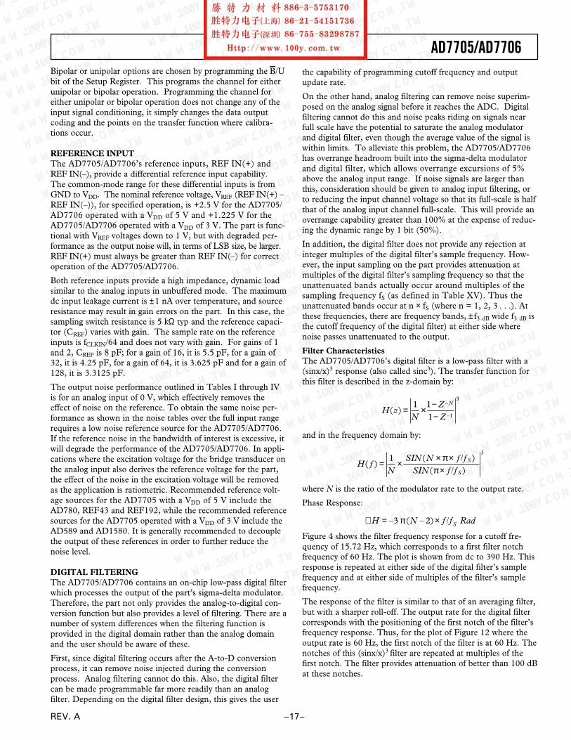
Figure 4 shows the filter frequency response for a cutoff fre-quency of 15.72 Hz, which corresponds to a first filter notchfrequency of 60 Hz. The plot is shown from dc to 390 Hz. Thisresponse is repeated at either side of the digital filter’s samplefrequency and at either side of multiples of the filter’s samplefrequency.
The response of the filter is similar to that of an averaging filter,but with a sharper roll-off. The output rate for the digital filtercorresponds with the positioning of the first notch of the filter’sfrequency response. Thus, for the plot of Figure 12 where theoutput rate is 60 Hz, the first notch of the filter is at 60 Hz. Thenotches of this (sinx/x)3 filter are repeated at multiples of thefirst notch. The filter provides attenuation of better than 100 dBat these notches.
AD7705/AD7706
–18– REV. A
The cutoff frequency of the digital filter is determined by thevalue loaded to bits FS0 to FS1 in the CLOCK Register. Pro-gramming a different cutoff frequency via FS0 and FS1 does notalter the profile of the filter response, it changes the frequency ofthe notches. The output update of the part and the frequency ofthe first notch correspond.
Since the AD7705/AD7706 contains this on-chip, low-passfiltering, a settling time is associated with step function inputsand data on the output will be invalid after a step change untilthe settling time has elapsed. The settling time depends uponthe output rate chosen for the filter. The settling time of thefilter to a full-scale step input can be up to four times the outputdata period. For a synchronized step input (using the FSYNCfunction), the settling time is three times the output data period.
FREQUENCY – Hz
0
–140
–2400
GA
IN –
dB
60 120 180 240 300 360
–20
–160
–180
–60
–100
–40
–80
–200
–220
–120
Figure 12. Frequency Response of AD7705 Filter
Post-FilteringThe on-chip modulator provides samples at a 19.2 kHz outputrate with fCLKIN at 2.4576 MHz. The on-chip digital filter deci-mates these samples to provide data at an output rate that corre-sponds to the programmed output rate of the filter. Since theoutput data rate is higher than the Nyquist criterion, the outputrate for a given bandwidth will satisfy most application require-ments. There may, however, be some applications which requirea higher data rate for a given bandwidth and noise performance.Applications that need this higher data rate will require somepost-filtering following the digital filter of the AD7705/AD7706.
For example, if the required bandwidth is 7.86 Hz, but therequired update rate is 100 Hz, the data can be taken from theAD7705/AD7706 at the 100 Hz rate giving a –3 dB bandwidthof 26.2 Hz. Post-filtering can be applied to this to reduce thebandwidth and output noise, to the 7.86 Hz bandwidth level,while maintaining an output rate of 100 Hz.
Post-filtering can also be used to reduce the output noise fromthe device for bandwidths below 13.1 Hz. At a gain of 128 anda bandwidth of 13.1 Hz, the output rms noise is 450 nV. Thisis essentially device noise or white noise and since the input ischopped, the noise has a primarily flat frequency response. Byreducing the bandwidth below 13.1 Hz, the noise in the result-ant passband can be reduced. A reduction in bandwidth by afactor of 2 results in a reduction of approximately 1.25 in theoutput rms noise. This additional filtering will result in a longersettling-time.
ANALOG FILTERINGThe digital filter does not provide any rejection at integer mul-tiples of the modulator sample frequency, as outlined earlier.However, due to the AD7705/AD7706’s high oversamplingratio, these bands occupy only a small fraction of the spectrumand most broadband noise is filtered. This means that the ana-log filtering requirements in front of the AD7705/AD7706 areconsiderably reduced versus a conventional converter with noon-chip filtering. In addition, because the part’s common-moderejection performance of 100 dB extends out to several kHz,common-mode noise in this frequency range will be substan-tially reduced.
Depending on the application, however, it may be necessary toprovide attenuation prior to the AD7705/AD7706 in order toeliminate unwanted frequencies from these bands which thedigital filter will pass. It may also be necessary in some applica-tions to provide analog filtering in front of the AD7705/AD7706to ensure that differential noise signals outside the band of inter-est do not saturate the analog modulator.
If passive components are placed in front of the AD7705/AD7706in unbuffered mode, care must be taken to ensure that thesource impedance is low enough not to introduce gain errors inthe system. This significantly limits the amount of passive anti-aliasing filtering which can be provided in front of the AD7705/AD7706 when it is used in unbuffered mode. However, whenthe part is used in buffered mode, large source impedances willsimply result in a small dc offset error (a 10 kΩ source resistancewill cause an offset error of less than 10 µV). Therefore, if thesystem requires any significant source impedances to providepassive analog filtering in front of the AD7705/AD7706, it isrecommended that the part be operated in buffered mode.
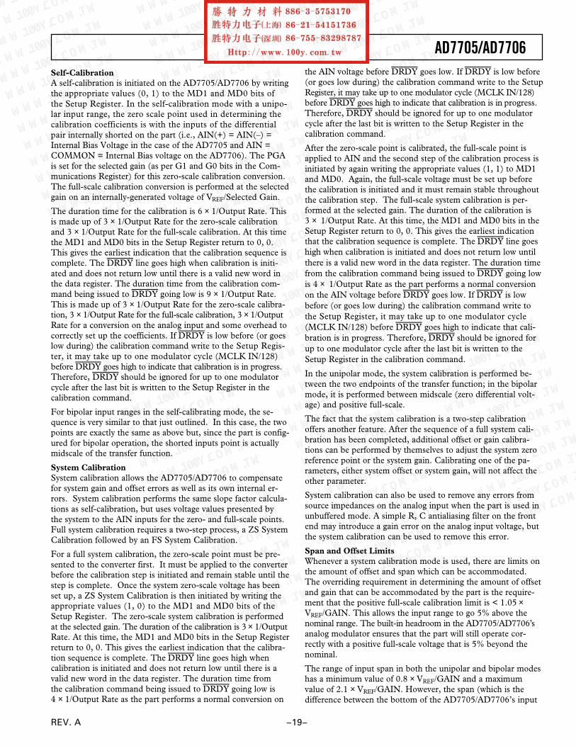
CALIBRATIONThe AD7705/AD7706 provides a number of calibration optionswhich can be programmed via the MD1 and MD0 bits of theSetup Register. The different calibration options are outlined inthe Setup Register and Calibration Sequences sections. A cali-bration cycle may be initiated at any time by writing to thesebits of the Setup Register. Calibration on the AD7705/AD7706removes offset and gain errors from the device. A calibrationroutine should be initiated on the device whenever there is achange in the ambient operating temperature or supply voltage.It should also be initiated if there is a change in the selectedgain, filter notch or bipolar/unipolar input range.
The AD7705/AD7706 offers self-calibration and system calibra-tion facilities. For full calibration to occur on the selected chan-nel, the on-chip microcontroller must record the modulatoroutput for two different input conditions. These are “zero-scale” and “full-scale” points. These points are derived byperforming a conversion on the different input voltages providedto the input of the modulator during calibration. As a result, theaccuracy of the calibration can only be as good as the noise levelthat it provides in normal mode. The result of the “zero-scale”calibration conversion is stored in the Zero-Scale CalibrationRegister while the result of the “full-scale” calibration conver-sion is stored in the Full-Scale Calibration Register. With thesereadings, the microcontroller can calculate the offset and thegain slope for the input-to-output transfer function of the con-verter. Internally, the part works with a resolution of 33 bits todetermine its conversion result of 16 bits.
AD7705/AD7706
–19–REV. A
Self-CalibrationA self-calibration is initiated on the AD7705/AD7706 by writingthe appropriate values (0, 1) to the MD1 and MD0 bits ofthe Setup Register. In the self-calibration mode with a unipo-lar input range, the zero scale point used in determining thecalibration coefficients is with the inputs of the differentialpair internally shorted on the part (i.e., AIN(+) = AIN(–) =Internal Bias Voltage in the case of the AD7705 and AIN =COMMON = Internal Bias voltage on the AD7706). The PGAis set for the selected gain (as per G1 and G0 bits in the Com-munications Register) for this zero-scale calibration conversion.The full-scale calibration conversion is performed at the selectedgain on an internally-generated voltage of VREF/Selected Gain.
The duration time for the calibration is 6 × 1/Output Rate. Thisis made up of 3 × 1/Output Rate for the zero-scale calibrationand 3 × 1/Output Rate for the full-scale calibration. At this timethe MD1 and MD0 bits in the Setup Register return to 0, 0.This gives the earliest indication that the calibration sequence iscomplete. The DRDY line goes high when calibration is initi-ated and does not return low until there is a valid new word inthe data register. The duration time from the calibration com-mand being issued to DRDY going low is 9 × 1/Output Rate.This is made up of 3 × 1/Output Rate for the zero-scale calibra-tion, 3 × 1/Output Rate for the full-scale calibration, 3 × 1/OutputRate for a conversion on the analog input and some overhead tocorrectly set up the coefficients. If DRDY is low before (or goeslow during) the calibration command write to the Setup Regis-ter, it may take up to one modulator cycle (MCLK IN/128)before DRDY goes high to indicate that calibration is in progress.Therefore, DRDY should be ignored for up to one modulatorcycle after the last bit is written to the Setup Register in thecalibration command.
For bipolar input ranges in the self-calibrating mode, the se-quence is very similar to that just outlined. In this case, the twopoints are exactly the same as above but, since the part is config-ured for bipolar operation, the shorted inputs point is actuallymidscale of the transfer function.
System CalibrationSystem calibration allows the AD7705/AD7706 to compensatefor system gain and offset errors as well as its own internal er-rors. System calibration performs the same slope factor calcula-tions as self-calibration, but uses voltage values presented bythe system to the AIN inputs for the zero- and full-scale points.Full system calibration requires a two-step process, a ZS SystemCalibration followed by an FS System Calibration.
For a full system calibration, the zero-scale point must be pre-sented to the converter first. It must be applied to the converterbefore the calibration step is initiated and remain stable until thestep is complete. Once the system zero-scale voltage has beenset up, a ZS System Calibration is then initiated by writing theappropriate values (1, 0) to the MD1 and MD0 bits of theSetup Register. The zero-scale system calibration is performedat the selected gain. The duration of the calibration is 3 × 1/OutputRate. At this time, the MD1 and MD0 bits in the Setup Registerreturn to 0, 0. This gives the earliest indication that the calibra-tion sequence is complete. The DRDY line goes high whencalibration is initiated and does not return low until there is avalid new word in the data register. The duration time fromthe calibration command being issued to DRDY going low is4 × 1/Output Rate as the part performs a normal conversion on
the AIN voltage before DRDY goes low. If DRDY is low before(or goes low during) the calibration command write to the SetupRegister, it may take up to one modulator cycle (MCLK IN/128)before DRDY goes high to indicate that calibration is in progress.Therefore, DRDY should be ignored for up to one modulatorcycle after the last bit is written to the Setup Register in thecalibration command.
After the zero-scale point is calibrated, the full-scale point isapplied to AIN and the second step of the calibration process isinitiated by again writing the appropriate values (1, 1) to MD1and MD0. Again, the full-scale voltage must be set up beforethe calibration is initiated and it must remain stable throughoutthe calibration step. The full-scale system calibration is per-formed at the selected gain. The duration of the calibration is3 × 1/Output Rate. At this time, the MD1 and MD0 bits in theSetup Register return to 0, 0. This gives the earliest indicationthat the calibration sequence is complete. The DRDY line goeshigh when calibration is initiated and does not return low untilthere is a valid new word in the data register. The duration timefrom the calibration command being issued to DRDY going lowis 4 × 1/Output Rate as the part performs a normal conversionon the AIN voltage before DRDY goes low. If DRDY is lowbefore (or goes low during) the calibration command write tothe Setup Register, it may take up to one modulator cycle(MCLK IN/128) before DRDY goes high to indicate that cali-bration is in progress. Therefore, DRDY should be ignored forup to one modulator cycle after the last bit is written to theSetup Register in the calibration command.
In the unipolar mode, the system calibration is performed be-tween the two endpoints of the transfer function; in the bipolarmode, it is performed between midscale (zero differential volt-age) and positive full-scale.
The fact that the system calibration is a two-step calibrationoffers another feature. After the sequence of a full system cali-bration has been completed, additional offset or gain calibra-tions can be performed by themselves to adjust the system zeroreference point or the system gain. Calibrating one of the pa-rameters, either system offset or system gain, will not affect theother parameter.
System calibration can also be used to remove any errors fromsource impedances on the analog input when the part is used inunbuffered mode. A simple R, C antialiasing filter on the frontend may introduce a gain error on the analog input voltage, butthe system calibration can be used to remove this error.
Span and Offset LimitsWhenever a system calibration mode is used, there are limits onthe amount of offset and span which can be accommodated.The overriding requirement in determining the amount of offsetand gain that can be accommodated by the part is the require-ment that the positive full-scale calibration limit is < 1.05 ×VREF/GAIN. This allows the input range to go 5% above thenominal range. The built-in headroom in the AD7705/AD7706’sanalog modulator ensures that the part will still operate cor-rectly with a positive full-scale voltage that is 5% beyond thenominal.
The range of input span in both the unipolar and bipolar modeshas a minimum value of 0.8 × VREF/GAIN and a maximumvalue of 2.1 × VREF/GAIN. However, the span (which is thedifference between the bottom of the AD7705/AD7706’s input
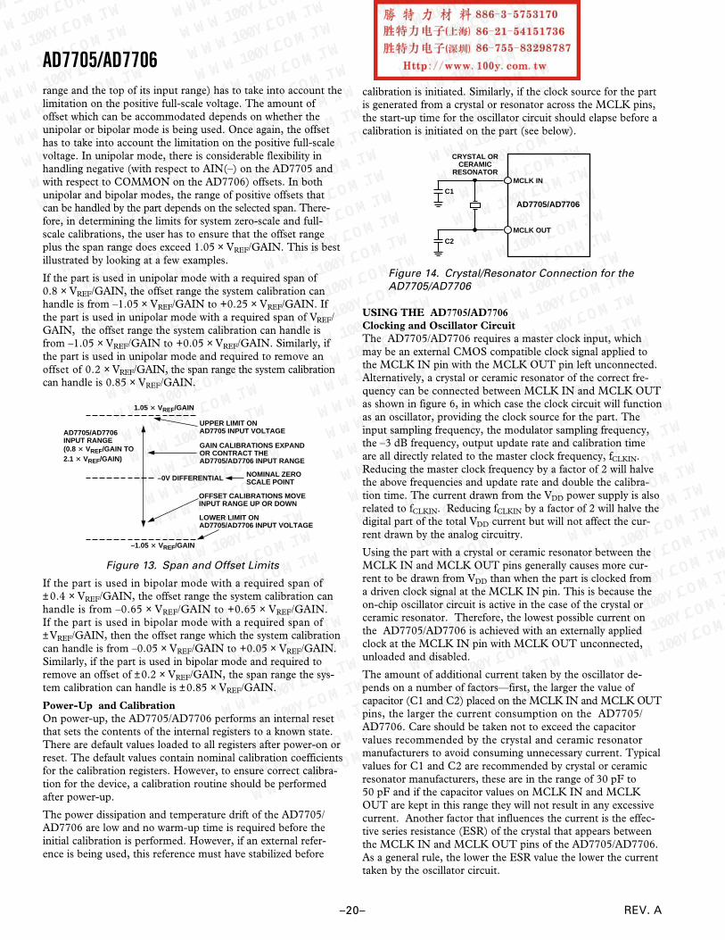
AD7705/AD7706
–20– REV. A
range and the top of its input range) has to take into account thelimitation on the positive full-scale voltage. The amount ofoffset which can be accommodated depends on whether theunipolar or bipolar mode is being used. Once again, the offsethas to take into account the limitation on the positive full-scalevoltage. In unipolar mode, there is considerable flexibility inhandling negative (with respect to AIN(–) on the AD7705 andwith respect to COMMON on the AD7706) offsets. In bothunipolar and bipolar modes, the range of positive offsets thatcan be handled by the part depends on the selected span. There-fore, in determining the limits for system zero-scale and full-scale calibrations, the user has to ensure that the offset rangeplus the span range does exceed 1.05 × VREF/GAIN. This is bestillustrated by looking at a few examples.
If the part is used in unipolar mode with a required span of0.8 × VREF/GAIN, the offset range the system calibration canhandle is from –1.05 × VREF/GAIN to +0.25 × VREF/GAIN. Ifthe part is used in unipolar mode with a required span of VREF/GAIN, the offset range the system calibration can handle isfrom –1.05 × VREF/GAIN to +0.05 × VREF/GAIN. Similarly, ifthe part is used in unipolar mode and required to remove anoffset of 0.2 × VREF/GAIN, the span range the system calibrationcan handle is 0.85 × VREF/GAIN.
AD7705/AD7706INPUT RANGE(0.8 3 VREF/GAIN TO2.1 3 VREF/GAIN)
UPPER LIMIT ONAD7705 INPUT VOLTAGE
NOMINAL ZEROSCALE POINT
OFFSET CALIBRATIONS MOVEINPUT RANGE UP OR DOWN
LOWER LIMIT ONAD7705/AD7706 INPUT VOLTAGE
–1.05 3 VREF/GAIN
–0V DIFFERENTIAL
GAIN CALIBRATIONS EXPANDOR CONTRACT THEAD7705/AD7706 INPUT RANGE
1.05 3 VREF/GAIN
Figure 13. Span and Offset Limits
If the part is used in bipolar mode with a required span of± 0.4 × VREF/GAIN, the offset range the system calibration canhandle is from –0.65 × VREF/GAIN to +0.65 × VREF/GAIN.If the part is used in bipolar mode with a required span of±VREF/GAIN, then the offset range which the system calibrationcan handle is from –0.05 × VREF/GAIN to +0.05 × VREF/GAIN.Similarly, if the part is used in bipolar mode and required toremove an offset of ±0.2 × VREF/GAIN, the span range the sys-tem calibration can handle is ±0.85 × VREF/GAIN.
Power-Up and CalibrationOn power-up, the AD7705/AD7706 performs an internal resetthat sets the contents of the internal registers to a known state.There are default values loaded to all registers after power-on orreset. The default values contain nominal calibration coefficientsfor the calibration registers. However, to ensure correct calibra-tion for the device, a calibration routine should be performedafter power-up.
The power dissipation and temperature drift of the AD7705/AD7706 are low and no warm-up time is required before theinitial calibration is performed. However, if an external refer-ence is being used, this reference must have stabilized before
calibration is initiated. Similarly, if the clock source for the partis generated from a crystal or resonator across the MCLK pins,the start-up time for the oscillator circuit should elapse before acalibration is initiated on the part (see below).
MCLK IN
MCLK OUT
CRYSTAL ORCERAMIC
RESONATOR
C1
C2
AD7705/AD7706
Figure 14. Crystal/Resonator Connection for theAD7705/AD7706
USING THE AD7705/AD7706Clocking and Oscillator CircuitThe AD7705/AD7706 requires a master clock input, whichmay be an external CMOS compatible clock signal applied tothe MCLK IN pin with the MCLK OUT pin left unconnected.Alternatively, a crystal or ceramic resonator of the correct fre-quency can be connected between MCLK IN and MCLK OUTas shown in figure 6, in which case the clock circuit will functionas an oscillator, providing the clock source for the part. Theinput sampling frequency, the modulator sampling frequency,the –3 dB frequency, output update rate and calibration timeare all directly related to the master clock frequency, fCLKIN.Reducing the master clock frequency by a factor of 2 will halvethe above frequencies and update rate and double the calibra-tion time. The current drawn from the VDD power supply is alsorelated to fCLKIN. Reducing fCLKIN by a factor of 2 will halve thedigital part of the total VDD current but will not affect the cur-rent drawn by the analog circuitry.
Using the part with a crystal or ceramic resonator between theMCLK IN and MCLK OUT pins generally causes more cur-rent to be drawn from VDD than when the part is clocked froma driven clock signal at the MCLK IN pin. This is because theon-chip oscillator circuit is active in the case of the crystal orceramic resonator. Therefore, the lowest possible current onthe AD7705/AD7706 is achieved with an externally appliedclock at the MCLK IN pin with MCLK OUT unconnected,unloaded and disabled.
The amount of additional current taken by the oscillator de-pends on a number of factors—first, the larger the value ofcapacitor (C1 and C2) placed on the MCLK IN and MCLK OUTpins, the larger the current consumption on the AD7705/AD7706. Care should be taken not to exceed the capacitorvalues recommended by the crystal and ceramic resonatormanufacturers to avoid consuming unnecessary current. Typicalvalues for C1 and C2 are recommended by crystal or ceramicresonator manufacturers, these are in the range of 30 pF to50 pF and if the capacitor values on MCLK IN and MCLKOUT are kept in this range they will not result in any excessivecurrent. Another factor that influences the current is the effec-tive series resistance (ESR) of the crystal that appears betweenthe MCLK IN and MCLK OUT pins of the AD7705/AD7706.As a general rule, the lower the ESR value the lower the currenttaken by the oscillator circuit.
AD7705/AD7706
–21–REV. A
When operating with a clock frequency of 2.4576 MHz, there is50 µA difference in the current between an externally appliedclock and a crystal resonator when operating with a VDD of+3 V. With VDD = +5 V and fCLKIN = 2.4576 MHz, the typicalcurrent increases by 250 µA for a crystal/resonator suppliedclock versus an externally applied clock. The ESR values forcrystals and resonators at this frequency tend to be low and as aresult there tends to be little difference between different crystaland resonator types.
When operating with a clock frequency of 1 MHz, the ESRvalue for different crystal types varies significantly. As a result,the current drain varies across crystal types. When using a crys-tal with an ESR of 700 Ω or when using a ceramic resonator, theincrease in the typical current over an externally-applied clock is20 µA with VDD = +3 V and 200 µA with VDD = +5 V. Whenusing a crystal with an ESR of 3 kΩ, the increase in the typicalcurrent over an externally applied clock is again 100 µA withVDD = +3 V but 400 µA with VDD = +5 V.
The on-chip oscillator circuit also has a start-up time associatedwith it before it is oscillating at its correct frequency and correctvoltage levels. Typical start-up times with VDD = 5 V are 6 msusing a 4.9512 MHz crystal, 16 ms with a 2.4576 MHz crystaland 20 ms with a 1 MHz crystal oscillator. Start-up times aretypically 20% slower when the power supply voltage is reducedto 3 V. At 3 V supplies, depending on the loading capacitanceson the MCLK pins, a 1 MΩ feedback resistor may be requiredacross the crystal or resonator in order to keep the start up timesaround the 20 ms duration.
The AD7705/AD7706’s master clock appears on the MCLKOUT pin of the device. The maximum recommended load onthis pin is one CMOS load. When using a crystal or ceramicresonator to generate the AD7705/AD7706’s clock, it may bedesirable to use this clock as the clock source for the system.In this case, it is recommended that the MCLK OUT signal isbuffered with a CMOS buffer before being applied to the rest ofthe circuit.
System SynchronizationThe FSYNC bit of the Setup Register allows the user to resetthe modulator and digital filter without affecting any of thesetup conditions on the part. This allows the user to start gath-ering samples of the analog input from a known point in time,i.e., when the FSYNC is changed from 1 to 0.
With a 1 in the FSYNC bit of the Setup Register, the digitalfilter and analog modulator are held in a known reset state andthe part is not processing any input samples. When a 0 is thenwritten to the FSYNC bit, the modulator and filter are takenout of this reset state and the part starts to gather samples againon the next master clock edge.
The FSYNC input can also be used as a software start convertcommand allowing the AD7705/AD7706 to be operated in aconventional converter fashion. In this mode, writing to theFSYNC bit starts conversion and the falling edge of DRDYindicates when conversion is complete. The disadvantage of thisscheme is that the settling time of the filter has to be taken intoaccount for every data register update. This means that the rateat which the data register is updated is three times slower in thismode.
Since the FSYNC bit resets the digital filter, the full settlingtime of 3 × 1/Output Rate has to elapse before there is a newword loaded to the output register on the part. If the DRDYsignal is low when FSYNC goes to a 0, the DRDY signal willnot be reset high by the FSYNC command. This is because theAD7705/AD7706 recognizes that there is a word in the dataregister which has not been read. The DRDY line will stay lowuntil an update of the data register takes place, at which time itwill go high for 500 × tCLKIN before returning low again. A readfrom the data register resets the DRDY signal high and it willnot return low until the settling time of the filter has elapsed(from the FSYNC command) and there is a valid new word inthe data register. If the DRDY line is high when the FSYNCcommand is issued, the DRDY line will not return low until thesettling time of the filter has elapsed.
Reset InputThe RESET input on the AD7705/AD7706 resets all the logic,the digital filter and the analog modulator, while all on-chipregisters are reset to their default state. DRDY is driven highand the AD7705/AD7706 ignores all communications to any ofits registers while the RESET input is low. When the RESETinput returns high, the AD7705/AD7706 starts to process dataand DRDY will return low in 3 × 1/Output Rate indicating avalid new word in the data register. However, the AD7705/AD7706 operates with its default setup conditions after aRESET and it is generally necessary to set up all registers andcarry out a calibration after a RESET command.
The AD7705/AD7706’s on-chip oscillator circuit continues tofunction even when the RESET input is low. The master clocksignal continues to be available on the MCLK OUT pin. There-fore, in applications where the system clock is provided by theAD7705/AD7706’s clock, the AD7705/AD7706 produces anuninterrupted master clock during RESET commands.
Standby ModeThe STBY bit in the Communications Register of the AD7705/AD7706 allows the user to place the part in a power-downmode when it is not required to provide conversion results. TheAD7705/AD7706 retains the contents of all its on-chip registers(including the data register) while in standby mode. When re-leased from standby mode, the part starts to process data and anew word is available in the data register in 3 × 1/Output ratefrom when a 0 is written to the STBY bit.
The STBY bit does not affect the digital interface, nor does itaffect the status of the DRDY line. If DRDY is high when theSTBY bit is brought low, it will remain high until there is a validnew word in the data register. If DRDY is low when the STBYbit is brought low, it will remain low until the data register isupdated, at which time the DRDY line will return high for500 × tCLKIN before returning low again. If DRDY is low whenthe part enters its standby mode (indicating a valid unread wordin the data register), the data register can be read while the partis in standby. At the end of this read operation, the DRDY willbe reset high as normal.
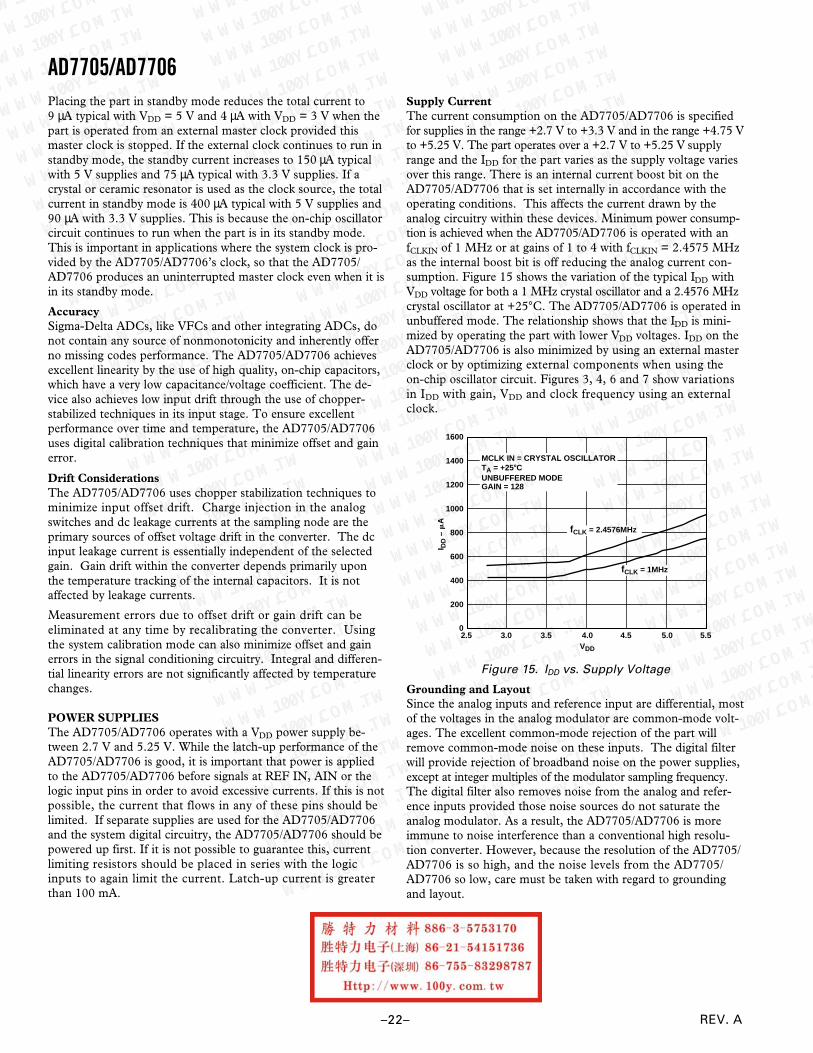
AD7705/AD7706
–22– REV. A
Placing the part in standby mode reduces the total current to9 µA typical with VDD = 5 V and 4 µA with VDD = 3 V when thepart is operated from an external master clock provided thismaster clock is stopped. If the external clock continues to run instandby mode, the standby current increases to 150 µA typicalwith 5 V supplies and 75 µA typical with 3.3 V supplies. If acrystal or ceramic resonator is used as the clock source, the totalcurrent in standby mode is 400 µA typical with 5 V supplies and90 µA with 3.3 V supplies. This is because the on-chip oscillatorcircuit continues to run when the part is in its standby mode.This is important in applications where the system clock is pro-vided by the AD7705/AD7706’s clock, so that the AD7705/AD7706 produces an uninterrupted master clock even when it isin its standby mode.
AccuracySigma-Delta ADCs, like VFCs and other integrating ADCs, donot contain any source of nonmonotonicity and inherently offerno missing codes performance. The AD7705/AD7706 achievesexcellent linearity by the use of high quality, on-chip capacitors,which have a very low capacitance/voltage coefficient. The de-vice also achieves low input drift through the use of chopper-stabilized techniques in its input stage. To ensure excellentperformance over time and temperature, the AD7705/AD7706uses digital calibration techniques that minimize offset and gainerror.
Drift ConsiderationsThe AD7705/AD7706 uses chopper stabilization techniques tominimize input offset drift. Charge injection in the analogswitches and dc leakage currents at the sampling node are theprimary sources of offset voltage drift in the converter. The dcinput leakage current is essentially independent of the selectedgain. Gain drift within the converter depends primarily uponthe temperature tracking of the internal capacitors. It is notaffected by leakage currents.
Measurement errors due to offset drift or gain drift can beeliminated at any time by recalibrating the converter. Usingthe system calibration mode can also minimize offset and gainerrors in the signal conditioning circuitry. Integral and differen-tial linearity errors are not significantly affected by temperaturechanges.
POWER SUPPLIESThe AD7705/AD7706 operates with a VDD power supply be-tween 2.7 V and 5.25 V. While the latch-up performance of theAD7705/AD7706 is good, it is important that power is appliedto the AD7705/AD7706 before signals at REF IN, AIN or thelogic input pins in order to avoid excessive currents. If this is notpossible, the current that flows in any of these pins should belimited. If separate supplies are used for the AD7705/AD7706and the system digital circuitry, the AD7705/AD7706 should bepowered up first. If it is not possible to guarantee this, currentlimiting resistors should be placed in series with the logicinputs to again limit the current. Latch-up current is greaterthan 100 mA.
Supply CurrentThe current consumption on the AD7705/AD7706 is specifiedfor supplies in the range +2.7 V to +3.3 V and in the range +4.75 Vto +5.25 V. The part operates over a +2.7 V to +5.25 V supplyrange and the IDD for the part varies as the supply voltage variesover this range. There is an internal current boost bit on theAD7705/AD7706 that is set internally in accordance with theoperating conditions. This affects the current drawn by theanalog circuitry within these devices. Minimum power consump-tion is achieved when the AD7705/AD7706 is operated with anfCLKIN of 1 MHz or at gains of 1 to 4 with fCLKIN = 2.4575 MHzas the internal boost bit is off reducing the analog current con-sumption. Figure 15 shows the variation of the typical IDD withVDD voltage for both a 1 MHz crystal oscillator and a 2.4576 MHzcrystal oscillator at +25°C. The AD7705/AD7706 is operated inunbuffered mode. The relationship shows that the IDD is mini-mized by operating the part with lower VDD voltages. IDD on theAD7705/AD7706 is also minimized by using an external masterclock or by optimizing external components when using theon-chip oscillator circuit. Figures 3, 4, 6 and 7 show variationsin IDD with gain, VDD and clock frequency using an externalclock.
VDD
1600
0
I DD
– m
A
1400
800
600
400
200
1200
1000
2.5 5.53.0 3.5 4.0 4.5 5.0
MCLK IN = CRYSTAL OSCILLATORTA = +258CUNBUFFERED MODEGAIN = 128
fCLK = 2.4576MHz
fCLK = 1MHz
Figure 15. IDD vs. Supply Voltage
Grounding and LayoutSince the analog inputs and reference input are differential, mostof the voltages in the analog modulator are common-mode volt-ages. The excellent common-mode rejection of the part willremove common-mode noise on these inputs. The digital filterwill provide rejection of broadband noise on the power supplies,except at integer multiples of the modulator sampling frequency.The digital filter also removes noise from the analog and refer-ence inputs provided those noise sources do not saturate theanalog modulator. As a result, the AD7705/AD7706 is moreimmune to noise interference than a conventional high resolu-tion converter. However, because the resolution of the AD7705/AD7706 is so high, and the noise levels from the AD7705/AD7706 so low, care must be taken with regard to groundingand layout.
AD7705/AD7706
–23–REV. A
The printed circuit board that houses the AD7705 should bedesigned so that the analog and digital sections are separatedand confined to certain areas of the board. This facilitates theuse of ground planes which can be separated easily. A minimumetch technique is generally best for ground planes as it gives thebest shielding. Digital and analog ground planes should only bejoined in one place to avoid ground loops. If the AD7705/AD7706is in a system where multiple devices require AGND-to-DGNDconnections, the connection should be made at one point only,a star ground point which should be established as close aspossible to the AD7705 GND.
Avoid running digital lines under the device as these will couplenoise onto the die. The analog ground plane should be allowedto run under the AD7705/AD7706 to avoid noise coupling. Thepower supply lines to the AD7705/AD7706 should use as largea trace as possible to provide low impedance paths and reducethe effects of glitches on the power supply line. Fast switchingsignals like clocks should be shielded with digital ground toavoid radiating noise to other sections of the board and clocksignals should never be run near the analog inputs. Avoid cross-over of digital and analog signals. Traces on opposite sides ofthe board should run at right angles to each other. This willreduce the effects of feedthrough through the board. A micro-strip technique is by far the best, but is not always possible witha double-sided board. In this technique, the component side ofthe board is dedicated to ground planes while signals are placedon the solder side.
Good decoupling is important when using high resolutionADCs. All analog supplies should be decoupled with 10 µFtantalum in parallel with 0.1 µF ceramic capacitors to GND. Toachieve the best from these decoupling components, they haveto be placed as close as possible to the device, ideally right upagainst the device. All logic chips should be decoupled with0.1 µF disc ceramic capacitors to DGND.
Evaluating the AD7705/AD7706 PerformanceThe recommended layout for the AD7705 and AD7706 is out-lined in their associated evaluation. These evaluation boardpackages include a fully assembled and tested evaluation board,documentation, software for controlling the board over theprinter port of a PC and software for analyzing their perfor-mance on the PC.
Noise levels in the signals applied to the AD7705/AD7706 mayalso affect performance of the part. The AD7705/AD7706 soft-ware evaluation package allows the user to evaluate the true
performance of the part, independent of the analog input signal.The scheme involves using a test mode on the part where theinputs to the AD7705 are internally shorted together to providea zero differential voltage for the analog modulator. External tothe device, the AIN1(–) input on the AD7705 should be con-nected to a voltage that is within the allowable common-moderange of the part. Similarly, on the AD7706 the COMMONinput should be connected to a voltage within its allowablecommon-mode range for evaluation purposes. This scheme shouldbe used after a calibration has been performed on the part.
DIGITAL INTERFACEAs previously outlined, the AD7705/AD7706’s programmablefunctions are controlled using a set of on-chip registers. Data iswritten to these registers via the part’s serial interface and readaccess to the on-chip registers is also provided by this interface.All communications to the part must start with a write operationto the Communications Register. After power-on or RESET,the device expects a write to its Communications Register. Thedata written to this register determines whether the next opera-tion to the part is a read or a write operation and also deter-mines to which register this read or write operation occurs.Therefore, write access to any of the other registers on the partstarts with a write operation to the Communications Registerfollowed by a write to the selected register. A read operationfrom any other register on the part (including the output dataregister) starts with a write operation to the CommunicationsRegister followed by a read operation from the selected register.
The AD7705/AD7706’s serial interface consists of five signals,CS, SCLK, DIN, DOUT and DRDY. The DIN line is used fortransferring data into the on-chip registers while the DOUT lineis used for accessing data from the on-chip registers. SCLK isthe serial clock input for the device and all data transfers (eitheron DIN or DOUT) take place with respect to this SCLK signal.The DRDY line is used as a status signal to indicate when datais ready to be read from the AD7705/AD7706’s data register.DRDY goes low when a new data word is available in the out-put register. It is reset high when a read operation from the dataregister is complete. It also goes high prior to the updating ofthe output register to indicate when not to read from the deviceto ensure that a data read is not attempted while the register isbeing updated. CS is used to select the device. It can be used todecode the AD7705/AD7706 in systems where a number ofparts are connected to the serial bus.
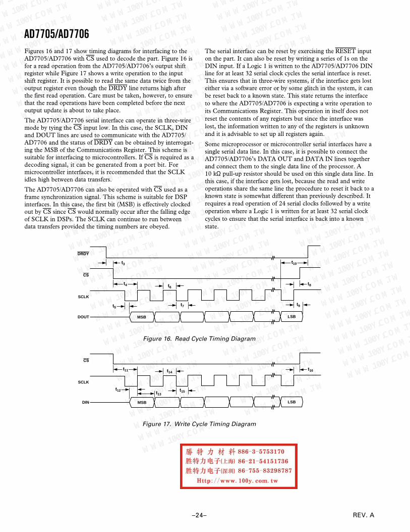
AD7705/AD7706
–24– REV. A
Figures 16 and 17 show timing diagrams for interfacing to theAD7705/AD7706 with CS used to decode the part. Figure 16 isfor a read operation from the AD7705/AD7706’s output shiftregister while Figure 17 shows a write operation to the inputshift register. It is possible to read the same data twice from theoutput register even though the DRDY line returns high afterthe first read operation. Care must be taken, however, to ensurethat the read operations have been completed before the nextoutput update is about to take place.
The AD7705/AD7706 serial interface can operate in three-wiremode by tying the CS input low. In this case, the SCLK, DINand DOUT lines are used to communicate with the AD7705/AD7706 and the status of DRDY can be obtained by interrogat-ing the MSB of the Communications Register. This scheme issuitable for interfacing to microcontrollers. If CS is required as adecoding signal, it can be generated from a port bit. Formicrocontroller interfaces, it is recommended that the SCLKidles high between data transfers.
The AD7705/AD7706 can also be operated with CS used as aframe synchronization signal. This scheme is suitable for DSPinterfaces. In this case, the first bit (MSB) is effectively clockedout by CS since CS would normally occur after the falling edgeof SCLK in DSPs. The SCLK can continue to run betweendata transfers provided the timing numbers are obeyed.
DRDY
CS
t3
t4 t6
t7t5
t10
t9
t8
SCLK
DOUT MSB LSB
Figure 16. Read Cycle Timing Diagram
CS
t11 t14
t15t12
t16
SCLK
DIN MSB LSB
t13
Figure 17. Write Cycle Timing Diagram
The serial interface can be reset by exercising the RESET inputon the part. It can also be reset by writing a series of 1s on theDIN input. If a Logic 1 is written to the AD7705/AD7706 DINline for at least 32 serial clock cycles the serial interface is reset.This ensures that in three-wire systems, if the interface gets losteither via a software error or by some glitch in the system, it canbe reset back to a known state. This state returns the interfaceto where the AD7705/AD7706 is expecting a write operation toits Communications Register. This operation in itself does notreset the contents of any registers but since the interface waslost, the information written to any of the registers is unknownand it is advisable to set up all registers again.
Some microprocessor or microcontroller serial interfaces have asingle serial data line. In this case, it is possible to connect theAD7705/AD7706’s DATA OUT and DATA IN lines togetherand connect them to the single data line of the processor. A10 kΩ pull-up resistor should be used on this single data line. Inthis case, if the interface gets lost, because the read and writeoperations share the same line the procedure to reset it back to aknown state is somewhat different than previously described. Itrequires a read operation of 24 serial clocks followed by a writeoperation where a Logic 1 is written for at least 32 serial clockcycles to ensure that the serial interface is back into a knownstate.
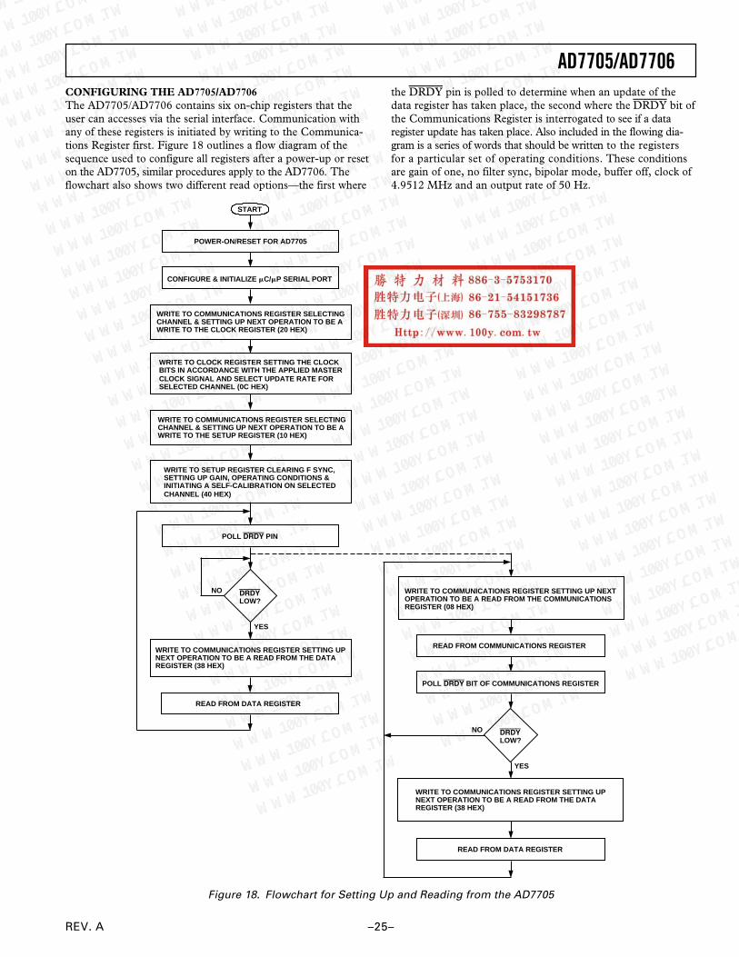
AD7705/AD7706
–25–REV. A
POWER-ON/RESET FOR AD7705
CONFIGURE & INITIALIZE mC/mP SERIAL PORT
WRITE TO COMMUNICATIONS REGISTER SELECTINGCHANNEL & SETTING UP NEXT OPERATION TO BE AWRITE TO THE CLOCK REGISTER (20 HEX)
WRITE TO CLOCK REGISTER SETTING THE CLOCKBITS IN ACCORDANCE WITH THE APPLIED MASTERCLOCK SIGNAL AND SELECT UPDATE RATE FORSELECTED CHANNEL (0C HEX)
WRITE TO COMMUNICATIONS REGISTER SELECTINGCHANNEL & SETTING UP NEXT OPERATION TO BE AWRITE TO THE SETUP REGISTER (10 HEX)
WRITE TO SETUP REGISTER CLEARING F SYNC,SETTING UP GAIN, OPERATING CONDITIONS &INITIATING A SELF-CALIBRATION ON SELECTEDCHANNEL (40 HEX)
POLL DRDY PIN
NO
YES
WRITE TO COMMUNICATIONS REGISTER SETTING UPNEXT OPERATION TO BE A READ FROM THE DATAREGISTER (38 HEX)
READ FROM DATA REGISTER
WRITE TO COMMUNICATIONS REGISTER SETTING UP NEXTOPERATION TO BE A READ FROM THE COMMUNICATIONSREGISTER (08 HEX)
READ FROM COMMUNICATIONS REGISTER
POLL DRDY BIT OF COMMUNICATIONS REGISTER
WRITE TO COMMUNICATIONS REGISTER SETTING UPNEXT OPERATION TO BE A READ FROM THE DATAREGISTER (38 HEX)
START
READ FROM DATA REGISTER
DRDYLOW?
NO
YES
DRDYLOW?
Figure 18. Flowchart for Setting Up and Reading from the AD7705
CONFIGURING THE AD7705/AD7706The AD7705/AD7706 contains six on-chip registers that theuser can accesses via the serial interface. Communication withany of these registers is initiated by writing to the Communica-tions Register first. Figure 18 outlines a flow diagram of thesequence used to configure all registers after a power-up or reseton the AD7705, similar procedures apply to the AD7706. Theflowchart also shows two different read options—the first where
the DRDY pin is polled to determine when an update of thedata register has taken place, the second where the DRDY bit ofthe Communications Register is interrogated to see if a dataregister update has taken place. Also included in the flowing dia-gram is a series of words that should be written to the registersfor a particular set of operating conditions. These conditionsare gain of one, no filter sync, bipolar mode, buffer off, clock of4.9512 MHz and an output rate of 50 Hz.
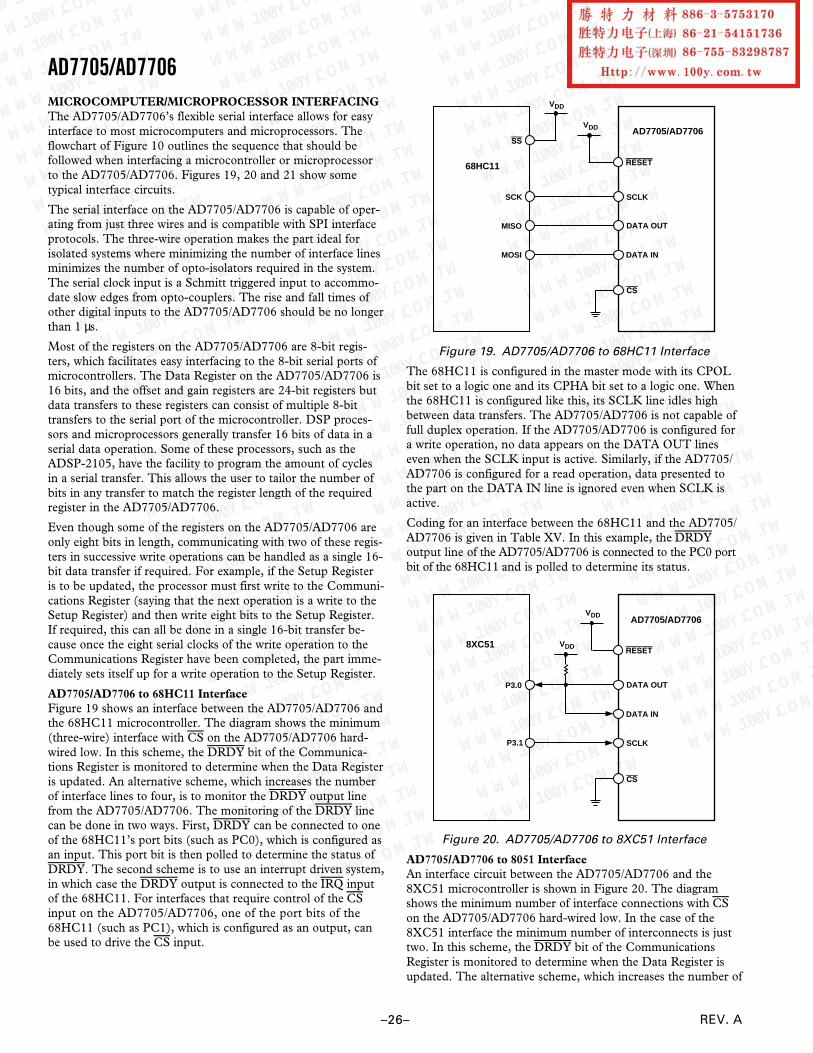
AD7705/AD7706
–26– REV. A
MICROCOMPUTER/MICROPROCESSOR INTERFACINGThe AD7705/AD7706’s flexible serial interface allows for easyinterface to most microcomputers and microprocessors. Theflowchart of Figure 10 outlines the sequence that should befollowed when interfacing a microcontroller or microprocessorto the AD7705/AD7706. Figures 19, 20 and 21 show sometypical interface circuits.
The serial interface on the AD7705/AD7706 is capable of oper-ating from just three wires and is compatible with SPI interfaceprotocols. The three-wire operation makes the part ideal forisolated systems where minimizing the number of interface linesminimizes the number of opto-isolators required in the system.The serial clock input is a Schmitt triggered input to accommo-date slow edges from opto-couplers. The rise and fall times ofother digital inputs to the AD7705/AD7706 should be no longerthan 1 µs.
Most of the registers on the AD7705/AD7706 are 8-bit regis-ters, which facilitates easy interfacing to the 8-bit serial ports ofmicrocontrollers. The Data Register on the AD7705/AD7706 is16 bits, and the offset and gain registers are 24-bit registers butdata transfers to these registers can consist of multiple 8-bittransfers to the serial port of the microcontroller. DSP proces-sors and microprocessors generally transfer 16 bits of data in aserial data operation. Some of these processors, such as theADSP-2105, have the facility to program the amount of cyclesin a serial transfer. This allows the user to tailor the number ofbits in any transfer to match the register length of the requiredregister in the AD7705/AD7706.
Even though some of the registers on the AD7705/AD7706 areonly eight bits in length, communicating with two of these regis-ters in successive write operations can be handled as a single 16-bit data transfer if required. For example, if the Setup Registeris to be updated, the processor must first write to the Communi-cations Register (saying that the next operation is a write to theSetup Register) and then write eight bits to the Setup Register.If required, this can all be done in a single 16-bit transfer be-cause once the eight serial clocks of the write operation to theCommunications Register have been completed, the part imme-diately sets itself up for a write operation to the Setup Register.
AD7705/AD7706 to 68HC11 InterfaceFigure 19 shows an interface between the AD7705/AD7706 andthe 68HC11 microcontroller. The diagram shows the minimum(three-wire) interface with CS on the AD7705/AD7706 hard-wired low. In this scheme, the DRDY bit of the Communica-tions Register is monitored to determine when the Data Registeris updated. An alternative scheme, which increases the numberof interface lines to four, is to monitor the DRDY output linefrom the AD7705/AD7706. The monitoring of the DRDY linecan be done in two ways. First, DRDY can be connected to oneof the 68HC11’s port bits (such as PC0), which is configured asan input. This port bit is then polled to determine the status ofDRDY. The second scheme is to use an interrupt driven system,in which case the DRDY output is connected to the IRQ inputof the 68HC11. For interfaces that require control of the CSinput on the AD7705/AD7706, one of the port bits of the68HC11 (such as PC1), which is configured as an output, canbe used to drive the CS input.
SS
SCK
MISO
MOSI
68HC11 RESET
SCLK
DATA OUT
DATA IN
CS
AD7705/AD7706
VDD
VDD
Figure 19. AD7705/AD7706 to 68HC11 Interface
The 68HC11 is configured in the master mode with its CPOLbit set to a logic one and its CPHA bit set to a logic one. Whenthe 68HC11 is configured like this, its SCLK line idles highbetween data transfers. The AD7705/AD7706 is not capable offull duplex operation. If the AD7705/AD7706 is configured fora write operation, no data appears on the DATA OUT lineseven when the SCLK input is active. Similarly, if the AD7705/AD7706 is configured for a read operation, data presented tothe part on the DATA IN line is ignored even when SCLK isactive.
Coding for an interface between the 68HC11 and the AD7705/AD7706 is given in Table XV. In this example, the DRDYoutput line of the AD7705/AD7706 is connected to the PC0 portbit of the 68HC11 and is polled to determine its status.
P3.0
P3.1
8XC51RESET
SCLK
DATA OUT
DATA IN
CS
AD7705/AD7706
VDD
VDD
Figure 20. AD7705/AD7706 to 8XC51 Interface
AD7705/AD7706 to 8051 InterfaceAn interface circuit between the AD7705/AD7706 and the8XC51 microcontroller is shown in Figure 20. The diagramshows the minimum number of interface connections with CSon the AD7705/AD7706 hard-wired low. In the case of the8XC51 interface the minimum number of interconnects is justtwo. In this scheme, the DRDY bit of the CommunicationsRegister is monitored to determine when the Data Register isupdated. The alternative scheme, which increases the number of

AD7705/AD7706
–27–REV. A
interface lines to three, is to monitor the DRDY output linefrom the AD7705/AD7706. The monitoring of the DRDY linecan be done in two ways. First, DRDY can be connected to oneof the 8XC51’s port bits (such as P1.0) which is configured asan input. This port bit is then polled to determine the status ofDRDY. The second scheme is to use an interrupt-driven system,in which case the DRDY output is connected to the INT1 inputof the 8XC51. For interfaces that require control of the CSinput on the AD7705/AD7706, one of the port bits of the8XC51 (such as P1.1), which is configured as an output, can beused to drive the CS input. The 8XC51 is configured in itsMode 0 serial interface mode. Its serial interface contains asingle data line. As a result, the DATA OUT and DATA INpins of the AD7705/AD7706 should be connected together witha 10 kΩ pull-up resistor. The serial clock on the 8XC51 idleshigh between data transfers. The 8XC51 outputs the LSB firstin a write operation, while the AD7705/AD7706 expects theMSB first so the data to be transmitted has to be rearrangedbefore being written to the output serial register. Similarly,the AD7705/AD7706 outputs the MSB first during a read op-eration while the 8XC51 expects the LSB first. Therefore, thedata read into the serial buffer needs to be rearranged before thecorrect data word from the AD7705/AD7706 is available in theaccumulator.
RFS
DT
ADSP-2103/ADSP-2105
RESET
SCLK
DATA OUT
DATA IN
CS
AD7705/AD7706VDD
TFS
DR
SCLK
Figure 21. AD7705/AD7706 to ADSP-2103/ADSP-2105Interface
AD7705/AD7706 to ADSP-2103/ADSP-2105 InterfaceFigure 21 shows an interface between the AD7705/AD7706 andthe ADSP-2103/ADSP-2105 DSP processor. In the interfaceshown, the DRDY bit of the Communications Register is againmonitored to determine when the Data Register is updated. Thealternative scheme is to use an interrupt-driven system, in whichcase the DRDY output is connected to the IRQ2 input of theADSP-2103/ADSP-2105. The serial interface of the ADSP-2103/ADSP-2105 is set up for alternate framing mode. TheRFS and TFS pins of the ADSP-2103/ADSP-2105 are config-ured as active low outputs and the ADSP-2103/ADSP-2105serial clock line, SCLK, is also configured as an output. The CSfor the AD7705/AD7706 is active when either the RFS or TFSoutputs from the ADSP-2103/ADSP-2105 are active. The serialclock rate on the ADSP-2103/ADSP-2105 should be limited to3 MHz to ensure correct operation with the AD7705/AD7706.
CODE FOR SETTING UP THE AD7705/AD7706Table XVII gives a set of read and write routines in C code forinterfacing the 68HC11 microcontroller to the AD7705. Thesample program sets up the various registers on the AD7705and reads 1000 samples from the part into the 68HC11. Thesetup conditions on the part are exactly the same as those out-lined for the flowchart of Figure 18. In the example code givenhere, the DRDY output is polled to determine if a new validword is available in the data register. The very same sequence isapplicable for the AD7706.
The sequence of the events in this program are as follows:
1. Write to the Communications Register, selecting channel oneas the active channel and setting the next operation to be awrite to the clock register.
2. Write to Clock Register setting the CLK DIV bit whichdivides the external clock internally by two. This assumesthat the external crystal is 4.9512 MHz. The update rate isselected to be 50 Hz.
3. Write to Communication Register selecting Channel 1 as theactive channel and setting the next operation to be a write tothe Setup Register.
4. Write to the Setup Register, setting the gain to 1, settingbipolar mode, buffer off, clearing the filter synchronizationand initiating a self-calibration.
5. Poll the DRDY output.
6. Read the data from the Data Register.
7. Loop around doing Steps 5 and 6 until the specified numberof samples have been taken from the selected channel.
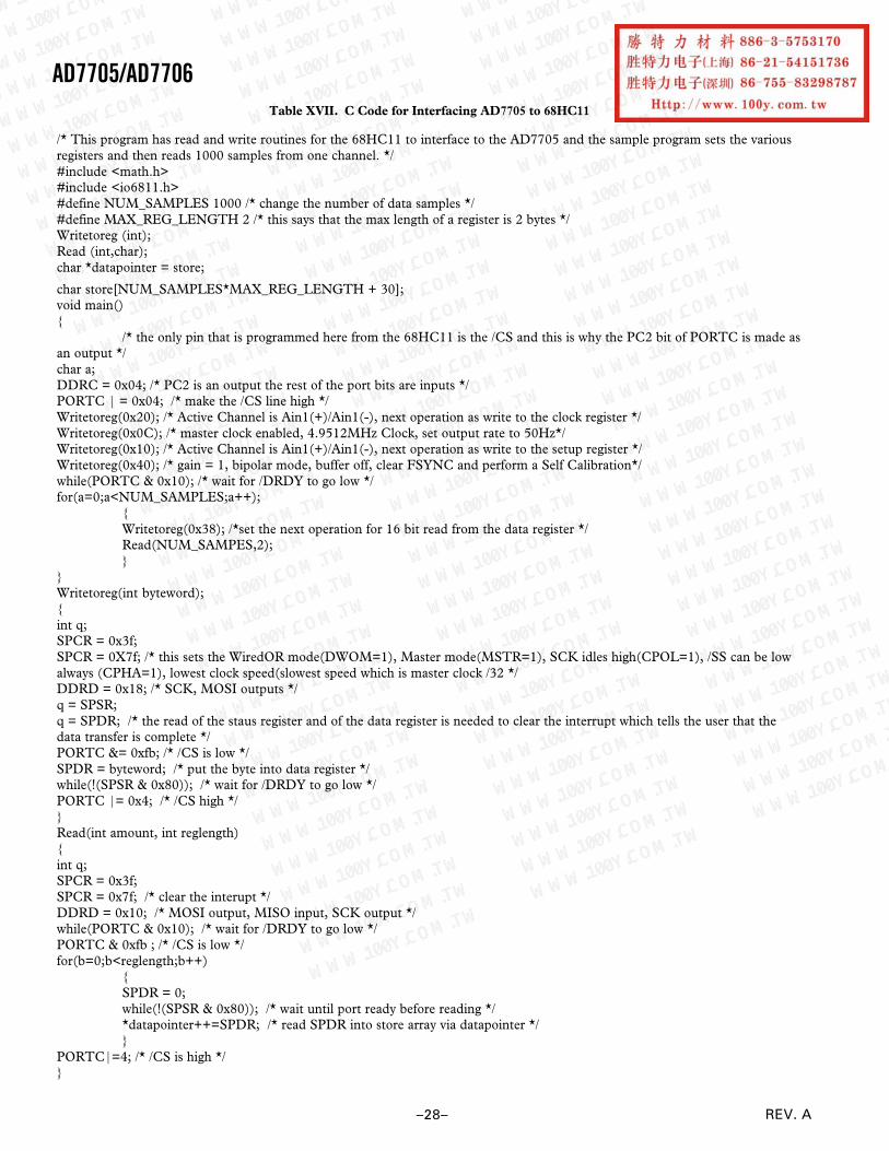
AD7705/AD7706
–28– REV. A
Table XVII. C Code for Interfacing AD7705 to 68HC11
/* This program has read and write routines for the 68HC11 to interface to the AD7705 and the sample program sets the variousregisters and then reads 1000 samples from one channel. */#include <math.h>#include <io6811.h>#define NUM_SAMPLES 1000 /* change the number of data samples */#define MAX_REG_LENGTH 2 /* this says that the max length of a register is 2 bytes */Writetoreg (int);Read (int,char);char *datapointer = store;
char store[NUM_SAMPLES*MAX_REG_LENGTH + 30];void main()
/* the only pin that is programmed here from the 68HC11 is the /CS and this is why the PC2 bit of PORTC is made asan output */char a;DDRC = 0x04; /* PC2 is an output the rest of the port bits are inputs */PORTC | = 0x04; /* make the /CS line high */Writetoreg(0x20); /* Active Channel is Ain1(+)/Ain1(-), next operation as write to the clock register */Writetoreg(0x0C); /* master clock enabled, 4.9512MHz Clock, set output rate to 50Hz*/Writetoreg(0x10); /* Active Channel is Ain1(+)/Ain1(-), next operation as write to the setup register */Writetoreg(0x40); /* gain = 1, bipolar mode, buffer off, clear FSYNC and perform a Self Calibration*/while(PORTC & 0x10); /* wait for /DRDY to go low */for(a=0;a<NUM_SAMPLES;a++);
Writetoreg(0x38); /*set the next operation for 16 bit read from the data register */Read(NUM_SAMPES,2);
Writetoreg(int byteword);int q;SPCR = 0x3f;SPCR = 0X7f; /* this sets the WiredOR mode(DWOM=1), Master mode(MSTR=1), SCK idles high(CPOL=1), /SS can be lowalways (CPHA=1), lowest clock speed(slowest speed which is master clock /32 */DDRD = 0x18; /* SCK, MOSI outputs */q = SPSR;q = SPDR; /* the read of the staus register and of the data register is needed to clear the interrupt which tells the user that thedata transfer is complete */PORTC &= 0xfb; /* /CS is low */SPDR = byteword; /* put the byte into data register */while(!(SPSR & 0x80)); /* wait for /DRDY to go low */PORTC |= 0x4; /* /CS high */Read(int amount, int reglength)int q;SPCR = 0x3f;SPCR = 0x7f; /* clear the interupt */DDRD = 0x10; /* MOSI output, MISO input, SCK output */while(PORTC & 0x10); /* wait for /DRDY to go low */PORTC & 0xfb ; /* /CS is low */for(b=0;b<reglength;b++)
SPDR = 0;while(!(SPSR & 0x80)); /* wait until port ready before reading */*datapointer++=SPDR; /* read SPDR into store array via datapointer */
PORTC|=4; /* /CS is high */
AD7705/AD7706
–29–REV. A
APPLICATIONSThe AD7705 provides a dual channel, low cost, high resolutionanalog-to-digital function. Because the analog-to-digital func-tion is provided by a sigma-delta architecture, it makes the partmore immune to noisy environments thus making the part idealfor use in industrial and process control applications. It alsoprovides a programmable gain amplifier, a digital filter andcalibration options. Thus, it provides far more system levelfunctionality than off-the-shelf integrating ADCs without thedisadvantage of having to supply a high quality integrating ca-pacitor. In addition, using the AD7705 in a system allows thesystem designer to achieve a much higher level of resolutionbecause noise performance of the AD7705 is better than that ofthe integrating ADCs.
The on-chip PGA allows the AD7705 to handle an analog inputvoltage range as low as 10 mV full-scale with VREF = +1.25 V.The differential inputs of the part allow this analog input rangeto have an absolute value anywhere between GND and VDD
when the part is operated in unbuffered mode. It allows the userto connect the transducer directly to the input of the AD7705.The programmable gain front end on the AD7705 allows thepart to handle unipolar analog input ranges from 0 mV to+20 mV to 0 V to +2.5 V and bipolar inputs of ±20 mV to±2.5 V. Because the part operates from a single supply thesebipolar ranges are with respect to a biased-up differential input.
AD7705
VDD
+5V
AIN1(+)
AIN1(–)
EXCITATION VOLTAGE = +5V
OUT(–)
IN–
OUT(+)
IN+
AIN2(+)
AIN2(–)
24kV
THERMOCOUPLEJUNCTION
15kV
REF IN(+)
REF IN(–)
GND
DOUT DIN CS SCLK
MCLK IN
MCLK OUT
RESET
DRDY
Figure 22. Pressure Measurement Using the AD7705
Pressure MeasurementOne typical application of the AD7705 is pressure measure-ment. Figure 22 shows the AD7705 used with a pressuretransducer, the BP01 from Sensym. The pressure transduceris arranged in a bridge network and gives a differential outputvoltage between its OUT(+) and OUT(–) terminals. With ratedfull-scale pressure (in this case 300 mmHg) on the transducer,the differential output voltage is 3 mV/V of the input voltage(i.e., the voltage between its IN(+) and IN(–) terminals).Assuming a 5 V excitation voltage, the full-scale output rangefrom the transducer is 15 mV. The excitation voltage for thebridge is also used to generate the reference voltage for theAD7705. Therefore, variations in the excitation voltage donot introduce errors in the system. Choosing resistor valuesof 24 kΩ and 15 kΩ, as per Figure 22, gives a 1.92 V referencevoltage for the AD7705 when the excitation voltage is 5 V.
Using the part with a programmed gain of 128 results in thefull-scale input span of the AD7705 being 15 mV, which corre-sponds with the output span from the transducer. The secondchannel on the AD7705 can be used as an auxiliary channel tomeasure a secondary variable such as temperature as shown inFigure 22. This secondary channel can be used as a means ofadjusting the output of the primary channel, thus removingtemperature effects in the system.
AD7705
VDD
+5V
AIN1(+)
AIN1(–)
THERMOCOUPLEJUNCTION
REF IN(+)
REF IN(–)
GND
MCLK IN
MCLK OUT
RESET
DRDY
REF192
GND
OUTPUT
DOUT DIN CS SCLK
+5V
Figure 23. Temperature Measurement Using the AD7705
Temperature MeasurementAnother application area for the AD7705 is in temperaturemeasurement. Figure 23 outlines a connection from a thermo-couple to the AD7705. In this application, the AD7705 is oper-ated in its buffered mode to allow large decoupling capacitorson the front end to eliminate any noise pickup that may havebeen in the thermocouple leads. When the AD7705 is operatedin buffered mode, it has a reduced common-mode range. Inorder to place the differential voltage from the thermocouple ona suitable common-mode voltage, the AIN1(–) input of theAD7705 is biased up at the reference voltage, +2.5 V.
Figure 23 shows another temperature measurement applicationfor the AD7705. In this case, the transducer is an RTD (Re-sistive Temperature Device), a PT100. The arrangement is a4-lead RTD configuration. There are voltage drops across thelead resistances RL1 and RL4 but these simply shift the common-mode voltage. There is no voltage drop across lead resistancesRL2 and RL3 as the input current to the AD7705 is very low.
The lead resistances present a small source impedance so itwould not generally be necessary to turn on the buffer on theAD7705. If the buffer is required, the common-mode voltageshould be set accordingly by inserting a small resistance be-tween the bottom end of the RTD and GND of the AD7705.In the application shown, an external 400 µA current sourceprovides the excitation current for the PT100 and also generatesthe reference voltage for the AD7705 via the 6.25 kΩ resistor.Variations in the excitation current do not affect the circuit asboth the input voltage and the reference voltage vary radiometri-cally with the excitation current. However, the 6.25 kΩ resistormust have a low temperature coefficient to avoid errors in thereference voltage over temperature.

AD7705/AD7706
–30– REV. A
AD7705
VDD
+5V
AIN1(+)
AIN1(–)
REF IN(–)
GND
MCLK IN
MCLK OUT
RESET
DRDY
DOUT DIN CS SCLK
REF IN(+)
6.25kV
400mA
RL1
RL2
RL3
RL4
RTD
Figure 24. RTD Measurement Using the AD7705
Smart TransmittersAnother area where the low power, single supply, three-wireinterface capabilities is of benefit is in smart transmitters. Here,the entire smart transmitter must operate from the 4 mA to20 mA loop. Tolerances in the loop mean that the amount ofcurrent available to power the transmitter is as low as 3.5 mA.The AD7705 consumes only 320 µA, leaving at least 3 mAavailable for the rest of the transmitter. Figure 25 shows a blockdiagram of a smart transmitter which includes the AD7705. TheAD7705 with its dual input channel is ideally suited to systemsrequiring an auxiliary channel whose measured variable is usedto correct that of the primary channel.
VDD
GND
REF IN
ISOLATED SUPPLY
4.7mF100kV
MCLK IN
MCLK OUT
AD7705
ISOLATED GROUND
MICROCONTROLLER UNIT
•PID•RANGE SETTING•CALIBRATION•LINEARIZATION•OUTPUT CONTROL•SERIAL COMMUNICATION•HART PROTOCOL
VCC
COM
VCC BOOST
REF OUT1
REF OUT2
REF IN
AD421
C1 C2 C3 COM
LOOPRTN
COMP
DRIVE
4.7mF
0.01mF
0.1mF2.2mFDN25D
1kV
1000pF
0.01mF
0.01mF
0.0033mF
ISOLATIONBARRIER
SENSORSRTDmV
VTC
MAIN TRANSMITTER ASSEMBLY
4mATO20mA
Figure 25. Smart Transmitter Using the AD7705
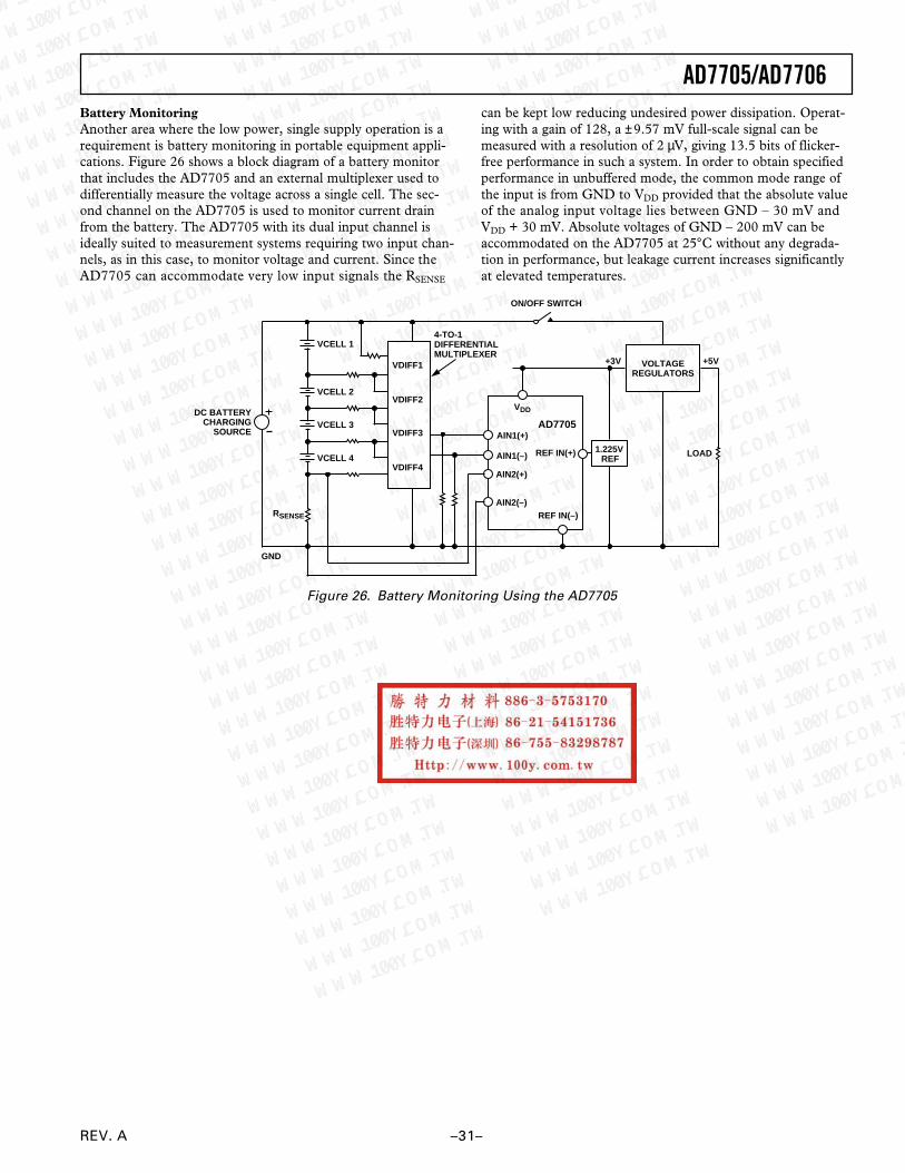
AD7705/AD7706
–31–REV. A
Battery MonitoringAnother area where the low power, single supply operation is arequirement is battery monitoring in portable equipment appli-cations. Figure 26 shows a block diagram of a battery monitorthat includes the AD7705 and an external multiplexer used todifferentially measure the voltage across a single cell. The sec-ond channel on the AD7705 is used to monitor current drainfrom the battery. The AD7705 with its dual input channel isideally suited to measurement systems requiring two input chan-nels, as in this case, to monitor voltage and current. Since theAD7705 can accommodate very low input signals the RSENSE
VCELL 1
RSENSE
AIN1(+)
AIN1(–)
AIN2(+)
AIN2(–)REF IN(–)
AD7705
VDD
REF IN(+) 1.225VREF
VOLTAGEREGULATORS
VCELL 2
VCELL 3
VCELL 4
VDIFF1
VDIFF2
VDIFF3
VDIFF4
DC BATTERYCHARGING
SOURCE
LOAD
ON/OFF SWITCH
+5V+3V
GND
4-TO-1DIFFERENTIALMULTIPLEXER
Figure 26. Battery Monitoring Using the AD7705
can be kept low reducing undesired power dissipation. Operat-ing with a gain of 128, a ±9.57 mV full-scale signal can bemeasured with a resolution of 2 µV, giving 13.5 bits of flicker-free performance in such a system. In order to obtain specifiedperformance in unbuffered mode, the common mode range ofthe input is from GND to VDD provided that the absolute valueof the analog input voltage lies between GND – 30 mV andVDD + 30 mV. Absolute voltages of GND – 200 mV can beaccommodated on the AD7705 at 25°C without any degrada-tion in performance, but leakage current increases significantlyat elevated temperatures.
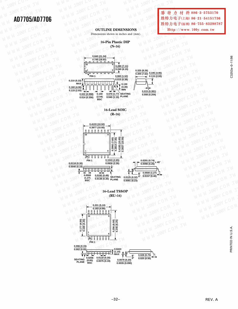
–32–
C32
53a–
0–11
/98
PR
INT
ED
IN U
.S.A
.
AD7705/AD7706
REV. A
OUTLINE DIMENSIONSDimensions shown in inches and (mm).
16-Pin Plastic DIP(N-16)
16
1 8
9
0.840 (21.34)0.745 (18.92)
0.280 (7.11)0.240 (6.10)
PIN 1
SEATINGPLANE
0.022 (0.558)0.014 (0.356)
0.060 (1.52)0.015 (0.38)0.210 (5.33)
MAX 0.130(3.30)MIN
0.070 (1.77)0.045 (1.15)
0.100(2.54)BSC
0.160 (4.06) 0.115 (2.93)
0.325 (8.26)0.300 (7.62)
0.015 (0.381)0.008 (0.204)
0.195 (4.95)0.115 (2.93)
16-Lead SOIC(R-16)
0.29
92 (
7.60
)0.
2914
(7.
40)
16 9
81
0.4133 (10.50)0.3977 (10.00)
0.41
93 (
10.6
5)0.
3937
(10
.00)
PIN 1
SEATINGPLANE
0.0118 (0.30)0.0040 (0.10)
0.0192 (0.49)0.0138 (0.35)
0.1043 (2.65)0.0926 (2.35)
0.0500(1.27)BSC
0.0125 (0.32)0.0091 (0.23)
0.0500 (1.27)0.0157 (0.40)
0.0291 (0.74)0.0098 (0.25)
x 458
8808
16-Lead TSSOP(RU-16)
16 9
81
0.201 (5.10)0.193 (4.90)
0.25
6 (6
.50)
0.24
6 (6
.25)
0.17
7 (4
.50)
0.16
9 (4
.30)
PIN 1
SEATINGPLANE
0.006 (0.15)0.002 (0.05)
0.0118 (0.30)0.0075 (0.19)
0.0256(0.65)BSC
0.0433(1.10)MAX
0.0079 (0.20)0.0035 (0.090)
0.028 (0.70)0.020 (0.50)
8°0°


